
diff options
| author | patrickmt <40182064+patrickmt@users.noreply.github.com> | 2018-08-29 15:07:52 -0400 |
|---|---|---|
| committer | Jack Humbert <jack.humb@gmail.com> | 2018-08-29 15:07:52 -0400 |
| commit | 30680c6eb396a2bb06928afd69edae9908ac84fb (patch) | |
| tree | a4a6c2598faa25dec208377a70dc0fb895ee9c8a | |
| parent | a6c770432f1348c44bc199029ce17b1b9ff4191c (diff) | |
Massdrop keyboard support (#3780)0.6.101
* Massdrop SAMD51
Massdrop SAMD51 keyboards initial project upload
* Removing relocated files
Removing files that were relocated and not deleted from previous location
* LED queue fix and cleaning
Cleaned some white space or comments.
Fix for LED I2C command queue.
Cleaned up interrupts.
Added debug function for printing numbers to scope through m15 line.
* Factory programmed serial usage
Ability to use factory programmed serial in hub and keyboard usb descriptors
* USB serial number and bugfix
Added support for factory programmed serial and usage.
Incorporated bootloader's conditional compiling to align project closer.
Fixed issue when USB device attempted to send before enabled.
General white space and comment cleanup.
* Project cleanup
Cleaned up project in terms of white space, commented code, and unecessary files.
NKRO keyboard is now using correct setreport although KBD was fine to use.
Fixed broken linkage to __xprintf for serial debug statements.
* Fix for extra keys
Fixed possible USB hang on extra keys report set missing
* I2C cleanup
I2C cleanup and file renames necessary for master branch merge
* Boot tracing and clocks cleanup
Added optional boot debug trace mode through debug LED codes.
General clock code cleanup.
* Relocate ARM/Atmel headers
Moved ARM/Atmel header folder from drivers to lib and made necessary makefile changes.
* Pull request changes
Pull request changes
* Keymap and compile flag fix
Keymap fix for momentary layer.
Potential compile flag fix for Travis CI failure.
* va_list include fix
Fix for va_list compile failure
* Include file case fixes
Fixes for include files with incorrect case
* ctrl and alt67 keyboard readme
Added ctrl and alt67 keyboard readme files
194 files changed, 73324 insertions, 1 deletions
diff --git a/build_keyboard.mk b/build_keyboard.mk index 9f6c42ea15..a73741bb3e 100644 --- a/build_keyboard.mk +++ b/build_keyboard.mk @@ -144,6 +144,9 @@ endif ifdef MCU_FAMILY FIRMWARE_FORMAT?=bin PLATFORM=CHIBIOS +else ifdef ARM_ATSAM + PLATFORM=ARM_ATSAM + FIRMWARE_FORMAT=bin else PLATFORM=AVR FIRMWARE_FORMAT?=hex @@ -286,6 +289,11 @@ endif include $(TMK_PATH)/avr.mk endif +ifeq ($(PLATFORM),ARM_ATSAM) + include $(TMK_PATH)/arm_atsam.mk + include $(TMK_PATH)/protocol/arm_atsam.mk +endif + ifeq ($(PLATFORM),CHIBIOS) include $(TMK_PATH)/protocol/chibios.mk endif diff --git a/keyboards/alt67/alt67.h b/keyboards/alt67/alt67.h new file mode 100644 index 0000000000..387985512b --- /dev/null +++ b/keyboards/alt67/alt67.h @@ -0,0 +1,24 @@ +#pragma once + +#include "quantum.h" +#include "config_led.h" +#include "matrix.h" + +#include "i2c_master.h" +#include "led_matrix.h" //For led keycodes +#include "usb/udi_cdc.h" +#include "usb/usb2422.h" + +#define LAYOUT( \ + K01, K02, K03, K04, K05, K06, K07, K08, K09, K10, K11, K12, K13, K14, K15, \ + K16, K17, K18, K19, K20, K21, K22, K23, K24, K25, K26, K27, K28, K29, K30, \ + K31, K32, K33, K34, K35, K36, K37, K38, K39, K40, K41, K42, K43, K44, K45, \ + K46, K47, K48, K49, K50, K51, K52, K53, K54, K55, K56, K57, K58, K59, K60, \ + K61, K62, K63, K64, K65, K66, K67 \ +) { \ + { K01, K02, K03, K04, K05, K06, K07, K08, K09, K10, K11, K12, K13, K14, K15, }, \ + { K16, K17, K18, K19, K20, K21, K22, K23, K24, K25, K26, K27, K28, K29, K30, }, \ + { K31, K32, K33, K34, K35, K36, K37, K38, K39, K40, K41, K42, KC_NO, K43, K44, }, \ + { K45, KC_NO, K46, K47, K48, K49, K50, K51, K52, K53, K54, K55, K56, K57, K58, }, \ + { K59, K60, K61, KC_NO, KC_NO, KC_NO, K62, KC_NO, KC_NO, KC_NO, K63, K64, K65, K66, K67, }, \ +} diff --git a/keyboards/alt67/config.h b/keyboards/alt67/config.h new file mode 100644 index 0000000000..c67ae7d432 --- /dev/null +++ b/keyboards/alt67/config.h @@ -0,0 +1,79 @@ +/* +Copyright 2015 Jun Wako <wakojun@gmail.com> + +This program is free software: you can redistribute it and/or modify +it under the terms of the GNU General Public License as published by +the Free Software Foundation, either version 2 of the License, or +(at your option) any later version. + +This program is distributed in the hope that it will be useful, +but WITHOUT ANY WARRANTY; without even the implied warranty of +MERCHANTABILITY or FITNESS FOR A PARTICULAR PURPOSE. See the +GNU General Public License for more details. + +You should have received a copy of the GNU General Public License +along with this program. If not, see <http://www.gnu.org/licenses/>. +*/ + +#pragma once + +#include "config_common.h" + +/* USB Device descriptor parameter */ +#define VENDOR_ID 0x04D8 +#define PRODUCT_ID 0xEED3 +#define DEVICE_VER 0x0101 + +#define MANUFACTURER "Massdrop Inc." +#define PRODUCT "ALT67 Keyboard" +#define SERIAL_NUM "Unavailable" + +/* key matrix size */ +#define MATRIX_ROWS 5 +#define MATRIX_COLS 15 + +#define PA 0 +#define PB 1 + +#define MATRIX_ROW_PORTS PA, PA, PA, PA, PA +#define MATRIX_ROW_PINS 0, 1, 2, 3, 4 + +#define MATRIX_COL_PORTS PB, PB, PB, PB, PB, PB, PB, PB, PB, PB, PA, PA, PA, PA, PA +#define MATRIX_COL_PINS 4, 5, 6, 7, 8, 9, 10, 11, 12, 13, 5, 6, 7, 10, 11 + +/* Print boot debug codes using debug LED when M28 and M30 shorted */ +#define DEBUG_BOOT_TRACING + +/* Debounce reduces chatter (unintended double-presses) - set 0 if debouncing is not needed */ +#define DEBOUNCING_DELAY 5 + +/* Mechanical locking support. Use KC_LCAP, KC_LNUM or KC_LSCR instead in keymap */ +//#define LOCKING_SUPPORT_ENABLE +/* Locking resynchronize hack */ +//#define LOCKING_RESYNC_ENABLE + +/* key combination for command */ +#define IS_COMMAND() ( \ + keyboard_report->mods == (MOD_BIT(KC_LSHIFT) | MOD_BIT(KC_RSHIFT)) \ +) + +/* Force boot in NKRO mode */ +//#define FORCE_NKRO + +/* + * Feature disable options + * These options are also useful to firmware size reduction. + */ + +/* disable debug print */ +//#define NO_DEBUG + +/* disable print */ +//#define NO_PRINT + +/* disable action features */ +//#define NO_ACTION_LAYER +//#define NO_ACTION_TAPPING +//#define NO_ACTION_ONESHOT +//#define NO_ACTION_MACRO +//#define NO_ACTION_FUNCTION diff --git a/keyboards/alt67/config_led.h b/keyboards/alt67/config_led.h new file mode 100644 index 0000000000..a049e38179 --- /dev/null +++ b/keyboards/alt67/config_led.h @@ -0,0 +1,178 @@ +/* +Copyright 2018 Massdrop Inc. + +This program is free software: you can redistribute it and/or modify +it under the terms of the GNU General Public License as published by +the Free Software Foundation, either version 2 of the License, or +(at your option) any later version. + +This program is distributed in the hope that it will be useful, +but WITHOUT ANY WARRANTY; without even the implied warranty of +MERCHANTABILITY or FITNESS FOR A PARTICULAR PURPOSE. See the +GNU General Public License for more details. + +You should have received a copy of the GNU General Public License +along with this program. If not, see <http://www.gnu.org/licenses/>. +*/ + +#ifndef _config_led_h_ +#define _config_led_h_ + +//Define number of ISSI3733 drivers being used (1...16) +#define ISSI3733_DRIVER_COUNT 2 + +//Hardware address of each driver (Refer to ISSI3733 pdf "Table 1 Slave Address" and keyboard schematic) +#define ISSI3773_DRIVER_ADDRESSES { 0xA0, 0xBE } + +//LED I2C bus speed +#define I2C_HZ 580000 + +//Count of LED bodies +#define ISSI3733_LED_COUNT 105 + +//Default Global Current Register value (Default brightness 0 - 255) +#define ISSI3733_GCR_DEFAULT 128 + +#define LED_GCR_MAX 165 //Max GCR value (0 - 255) WARNING: Raising this value may overload the LED drivers and USB bus +#define LED_GCR_STEP 10 //GCR increment/decrement value + +//Automatic power rollback and recovery +#define V5_HIGH 2540 //5V high level (After low power detect, point at which LEDs are allowed to use more power ) +#define V5_LOW 2480 //5V low level (LED power rolled back to stay above this limit) +#define V5_CAT 2200 //5V catastrophic level (Host USB port potential to shut down) + +#define ANIMATION_SPEED_STEP 1 + +#define BREATHE_MIN_STEP 0 +#define BREATHE_MAX_STEP 255 + +//LED Mapping - More practically generated from a spreadsheet program +//id: ID of the LED (Sync with PCB callouts) +//x: Physical X coordinate of LED (units do not matter) +//y: Physical Y coordinate of LED (units do not matter) +//drv: 1-Based index of ISSI3773_DRIVER_ADDRESSES +//cs: Matrix wiring CS col (1-16) +//swr: Matrix wiring SW Red row (1-12) +//swg: Matrix wiring SW Green row (1-12) +//swb: Matrix wiring SW Blue row (1-12) +//scan: Associated key scancode if any +//Note: Origin 0,0 may be located anywhere as the software will do the final layout +#define ISSI3733_LED_MAP { \ + { .id = 1, .x = 0, .y = 0, .adr = { .drv = 2, .cs = 2, .swr = 2, .swg = 1, .swb = 3 }, .scan = 0 }, \ + { .id = 2, .x = 0.75, .y = 0, .adr = { .drv = 2, .cs = 3, .swr = 5, .swg = 4, .swb = 6 }, .scan = 1 }, \ + { .id = 3, .x = 1.5, .y = 0, .adr = { .drv = 2, .cs = 4, .swr = 5, .swg = 4, .swb = 6 }, .scan = 2 }, \ + { .id = 4, .x = 2.25, .y = 0, .adr = { .drv = 2, .cs = 5, .swr = 5, .swg = 4, .swb = 6 }, .scan = 3 }, \ + { .id = 5, .x = 3, .y = 0, .adr = { .drv = 2, .cs = 6, .swr = 5, .swg = 4, .swb = 6 }, .scan = 4 }, \ + { .id = 6, .x = 3.75, .y = 0, .adr = { .drv = 2, .cs = 7, .swr = 5, .swg = 4, .swb = 6 }, .scan = 5 }, \ + { .id = 7, .x = 4.5, .y = 0, .adr = { .drv = 2, .cs = 8, .swr = 5, .swg = 4, .swb = 6 }, .scan = 6 }, \ + { .id = 8, .x = 5.25, .y = 0, .adr = { .drv = 2, .cs = 13, .swr = 2, .swg = 1, .swb = 3 }, .scan = 7 }, \ + { .id = 9, .x = 6, .y = 0, .adr = { .drv = 1, .cs = 1, .swr = 5, .swg = 4, .swb = 6 }, .scan = 8 }, \ + { .id = 10, .x = 6.75, .y = 0, .adr = { .drv = 1, .cs = 2, .swr = 5, .swg = 4, .swb = 6 }, .scan = 9 }, \ + { .id = 11, .x = 7.5, .y = 0, .adr = { .drv = 1, .cs = 3, .swr = 5, .swg = 4, .swb = 6 }, .scan = 10 }, \ + { .id = 12, .x = 8.25, .y = 0, .adr = { .drv = 1, .cs = 4, .swr = 5, .swg = 4, .swb = 6 }, .scan = 11 }, \ + { .id = 13, .x = 9, .y = 0, .adr = { .drv = 1, .cs = 5, .swr = 5, .swg = 4, .swb = 6 }, .scan = 12 }, \ + { .id = 14, .x = 10.125, .y = 0, .adr = { .drv = 1, .cs = 6, .swr = 5, .swg = 4, .swb = 6 }, .scan = 13 }, \ + { .id = 15, .x = 11.25, .y = 0, .adr = { .drv = 1, .cs = 7, .swr = 2, .swg = 1, .swb = 3 }, .scan = 14 }, \ + { .id = 16, .x = 0.188, .y = -0.75, .adr = { .drv = 2, .cs = 2, .swr = 5, .swg = 4, .swb = 6 }, .scan = 15 }, \ + { .id = 17, .x = 1.125, .y = -0.75, .adr = { .drv = 2, .cs = 3, .swr = 8, .swg = 7, .swb = 9 }, .scan = 16 }, \ + { .id = 18, .x = 1.875, .y = -0.75, .adr = { .drv = 2, .cs = 4, .swr = 8, .swg = 7, .swb = 9 }, .scan = 17 }, \ + { .id = 19, .x = 2.625, .y = -0.75, .adr = { .drv = 2, .cs = 5, .swr = 8, .swg = 7, .swb = 9 }, .scan = 18 }, \ + { .id = 20, .x = 3.375, .y = -0.75, .adr = { .drv = 2, .cs = 6, .swr = 8, .swg = 7, .swb = 9 }, .scan = 19 }, \ + { .id = 21, .x = 4.125, .y = -0.75, .adr = { .drv = 2, .cs = 7, .swr = 8, .swg = 7, .swb = 9 }, .scan = 20 }, \ + { .id = 22, .x = 4.875, .y = -0.75, .adr = { .drv = 2, .cs = 8, .swr = 8, .swg = 7, .swb = 9 }, .scan = 21 }, \ + { .id = 23, .x = 5.625, .y = -0.75, .adr = { .drv = 1, .cs = 1, .swr = 8, .swg = 7, .swb = 9 }, .scan = 22 }, \ + { .id = 24, .x = 6.375, .y = -0.75, .adr = { .drv = 1, .cs = 2, .swr = 8, .swg = 7, .swb = 9 }, .scan = 23 }, \ + { .id = 25, .x = 7.125, .y = -0.75, .adr = { .drv = 1, .cs = 3, .swr = 8, .swg = 7, .swb = 9 }, .scan = 24 }, \ + { .id = 26, .x = 7.875, .y = -0.75, .adr = { .drv = 1, .cs = 4, .swr = 8, .swg = 7, .swb = 9 }, .scan = 25 }, \ + { .id = 27, .x = 8.625, .y = -0.75, .adr = { .drv = 1, .cs = 5, .swr = 8, .swg = 7, .swb = 9 }, .scan = 26 }, \ + { .id = 28, .x = 9.375, .y = -0.75, .adr = { .drv = 1, .cs = 11, .swr = 11, .swg = 10, .swb = 12 }, .scan = 27 }, \ + { .id = 29, .x = 10.313, .y = -0.75, .adr = { .drv = 1, .cs = 6, .swr = 8, .swg = 7, .swb = 9 }, .scan = 28 }, \ + { .id = 30, .x = 11.25, .y = -0.75, .adr = { .drv = 1, .cs = 7, .swr = 5, .swg = 4, .swb = 6 }, .scan = 29 }, \ + { .id = 31, .x = 0.281, .y = -1.5, .adr = { .drv = 2, .cs = 2, .swr = 8, .swg = 7, .swb = 9 }, .scan = 30 }, \ + { .id = 32, .x = 1.313, .y = -1.5, .adr = { .drv = 2, .cs = 3, .swr = 11, .swg = 10, .swb = 12 }, .scan = 31 }, \ + { .id = 33, .x = 2.063, .y = -1.5, .adr = { .drv = 2, .cs = 4, .swr = 11, .swg = 10, .swb = 12 }, .scan = 32 }, \ + { .id = 34, .x = 2.813, .y = -1.5, .adr = { .drv = 2, .cs = 5, .swr = 11, .swg = 10, .swb = 12 }, .scan = 33 }, \ + { .id = 35, .x = 3.563, .y = -1.5, .adr = { .drv = 2, .cs = 6, .swr = 11, .swg = 10, .swb = 12 }, .scan = 34 }, \ + { .id = 36, .x = 4.313, .y = -1.5, .adr = { .drv = 2, .cs = 7, .swr = 11, .swg = 10, .swb = 12 }, .scan = 35 }, \ + { .id = 37, .x = 5.063, .y = -1.5, .adr = { .drv = 2, .cs = 8, .swr = 11, .swg = 10, .swb = 12 }, .scan = 36 }, \ + { .id = 38, .x = 5.813, .y = -1.5, .adr = { .drv = 1, .cs = 1, .swr = 11, .swg = 10, .swb = 12 }, .scan = 37 }, \ + { .id = 39, .x = 6.563, .y = -1.5, .adr = { .drv = 1, .cs = 2, .swr = 11, .swg = 10, .swb = 12 }, .scan = 38 }, \ + { .id = 40, .x = 7.313, .y = -1.5, .adr = { .drv = 1, .cs = 3, .swr = 11, .swg = 10, .swb = 12 }, .scan = 39 }, \ + { .id = 41, .x = 8.063, .y = -1.5, .adr = { .drv = 1, .cs = 4, .swr = 11, .swg = 10, .swb = 12 }, .scan = 40 }, \ + { .id = 42, .x = 8.813, .y = -1.5, .adr = { .drv = 1, .cs = 5, .swr = 11, .swg = 10, .swb = 12 }, .scan = 41 }, \ + { .id = 43, .x = 10.031, .y = -1.5, .adr = { .drv = 1, .cs = 6, .swr = 11, .swg = 10, .swb = 12 }, .scan = 43 }, \ + { .id = 44, .x = 11.25, .y = -1.5, .adr = { .drv = 1, .cs = 7, .swr = 8, .swg = 7, .swb = 9 }, .scan = 44 }, \ + { .id = 45, .x = 0.469, .y = -2.25, .adr = { .drv = 2, .cs = 2, .swr = 11, .swg = 10, .swb = 12 }, .scan = 45 }, \ + { .id = 46, .x = 1.688, .y = -2.25, .adr = { .drv = 2, .cs = 9, .swr = 5, .swg = 4, .swb = 6 }, .scan = 47 }, \ + { .id = 47, .x = 2.438, .y = -2.25, .adr = { .drv = 2, .cs = 9, .swr = 2, .swg = 1, .swb = 3 }, .scan = 48 }, \ + { .id = 48, .x = 3.188, .y = -2.25, .adr = { .drv = 2, .cs = 9, .swr = 11, .swg = 10, .swb = 12 }, .scan = 49 }, \ + { .id = 49, .x = 3.938, .y = -2.25, .adr = { .drv = 2, .cs = 9, .swr = 8, .swg = 7, .swb = 9 }, .scan = 50 }, \ + { .id = 50, .x = 4.688, .y = -2.25, .adr = { .drv = 2, .cs = 12, .swr = 11, .swg = 10, .swb = 12 }, .scan = 51 }, \ + { .id = 51, .x = 5.438, .y = -2.25, .adr = { .drv = 2, .cs = 13, .swr = 11, .swg = 10, .swb = 12 }, .scan = 52 }, \ + { .id = 52, .x = 6.188, .y = -2.25, .adr = { .drv = 1, .cs = 9, .swr = 11, .swg = 10, .swb = 12 }, .scan = 53 }, \ + { .id = 53, .x = 6.938, .y = -2.25, .adr = { .drv = 1, .cs = 10, .swr = 11, .swg = 10, .swb = 12 }, .scan = 54 }, \ + { .id = 54, .x = 7.688, .y = -2.25, .adr = { .drv = 1, .cs = 10, .swr = 8, .swg = 7, .swb = 9 }, .scan = 55 }, \ + { .id = 55, .x = 8.438, .y = -2.25, .adr = { .drv = 1, .cs = 11, .swr = 8, .swg = 7, .swb = 9 }, .scan = 56 }, \ + { .id = 56, .x = 9.469, .y = -2.25, .adr = { .drv = 1, .cs = 11, .swr = 2, .swg = 1, .swb = 3 }, .scan = 57 }, \ + { .id = 57, .x = 10.5, .y = -2.25, .adr = { .drv = 1, .cs = 11, .swr = 5, .swg = 4, .swb = 6 }, .scan = 58 }, \ + { .id = 58, .x = 11.25, .y = -2.25, .adr = { .drv = 1, .cs = 7, .swr = 11, .swg = 10, .swb = 12 }, .scan = 59 }, \ + { .id = 59, .x = 0.094, .y = -3, .adr = { .drv = 2, .cs = 10, .swr = 8, .swg = 7, .swb = 9 }, .scan = 60 }, \ + { .id = 60, .x = 1.031, .y = -3, .adr = { .drv = 2, .cs = 10, .swr = 5, .swg = 4, .swb = 6 }, .scan = 61 }, \ + { .id = 61, .x = 1.969, .y = -3, .adr = { .drv = 2, .cs = 10, .swr = 2, .swg = 1, .swb = 3 }, .scan = 62 }, \ + { .id = 62, .x = 4.781, .y = -3, .adr = { .drv = 2, .cs = 12, .swr = 8, .swg = 7, .swb = 9 }, .scan = 66 }, \ + { .id = 63, .x = 7.594, .y = -3, .adr = { .drv = 1, .cs = 10, .swr = 5, .swg = 4, .swb = 6 }, .scan = 70 }, \ + { .id = 64, .x = 8.531, .y = -3, .adr = { .drv = 1, .cs = 10, .swr = 2, .swg = 1, .swb = 3 }, .scan = 71 }, \ + { .id = 65, .x = 9.75, .y = -3, .adr = { .drv = 1, .cs = 12, .swr = 2, .swg = 1, .swb = 3 }, .scan = 72 }, \ + { .id = 66, .x = 10.5, .y = -3, .adr = { .drv = 1, .cs = 12, .swr = 8, .swg = 7, .swb = 9 }, .scan = 73 }, \ + { .id = 67, .x = 11.25, .y = -3, .adr = { .drv = 1, .cs = 12, .swr = 5, .swg = 4, .swb = 6 }, .scan = 74 }, \ + { .id = 68, .x = -0.338, .y = -3.338, .adr = { .drv = 2, .cs = 11, .swr = 11, .swg = 10, .swb = 12 }, .scan = 255 }, \ + { .id = 69, .x = 0.39, .y = -3.443, .adr = { .drv = 2, .cs = 11, .swr = 8, .swg = 7, .swb = 9 }, .scan = 255 }, \ + { .id = 70, .x = 1.263, .y = -3.443, .adr = { .drv = 2, .cs = 11, .swr = 5, .swg = 4, .swb = 6 }, .scan = 255 }, \ + { .id = 71, .x = 2.135, .y = -3.443, .adr = { .drv = 2, .cs = 11, .swr = 2, .swg = 1, .swb = 3 }, .scan = 255 }, \ + { .id = 72, .x = 3.008, .y = -3.443, .adr = { .drv = 2, .cs = 12, .swr = 2, .swg = 1, .swb = 3 }, .scan = 255 }, \ + { .id = 73, .x = 3.88, .y = -3.443, .adr = { .drv = 2, .cs = 12, .swr = 5, .swg = 4, .swb = 6 }, .scan = 255 }, \ + { .id = 74, .x = 4.753, .y = -3.443, .adr = { .drv = 2, .cs = 13, .swr = 5, .swg = 4, .swb = 6 }, .scan = 255 }, \ + { .id = 75, .x = 5.625, .y = -3.443, .adr = { .drv = 2, .cs = 13, .swr = 8, .swg = 7, .swb = 9 }, .scan = 255 }, \ + { .id = 76, .x = 6.497, .y = -3.443, .adr = { .drv = 1, .cs = 9, .swr = 8, .swg = 7, .swb = 9 }, .scan = 255 }, \ + { .id = 77, .x = 7.37, .y = -3.443, .adr = { .drv = 1, .cs = 9, .swr = 5, .swg = 4, .swb = 6 }, .scan = 255 }, \ + { .id = 78, .x = 8.242, .y = -3.443, .adr = { .drv = 1, .cs = 9, .swr = 2, .swg = 1, .swb = 3 }, .scan = 255 }, \ + { .id = 79, .x = 9.115, .y = -3.443, .adr = { .drv = 1, .cs = 13, .swr = 2, .swg = 1, .swb = 3 }, .scan = 255 }, \ + { .id = 80, .x = 9.987, .y = -3.443, .adr = { .drv = 1, .cs = 13, .swr = 8, .swg = 7, .swb = 9 }, .scan = 255 }, \ + { .id = 81, .x = 10.86, .y = -3.443, .adr = { .drv = 1, .cs = 13, .swr = 5, .swg = 4, .swb = 6 }, .scan = 255 }, \ + { .id = 82, .x = 11.588, .y = -3.338, .adr = { .drv = 1, .cs = 13, .swr = 11, .swg = 10, .swb = 12 }, .scan = 255 }, \ + { .id = 83, .x = 11.693, .y = -2.623, .adr = { .drv = 1, .cs = 12, .swr = 11, .swg = 10, .swb = 12 }, .scan = 255 }, \ + { .id = 84, .x = 11.693, .y = -1.873, .adr = { .drv = 1, .cs = 8, .swr = 11, .swg = 10, .swb = 12 }, .scan = 255 }, \ + { .id = 85, .x = 11.693, .y = -1.123, .adr = { .drv = 1, .cs = 8, .swr = 8, .swg = 7, .swb = 9 }, .scan = 255 }, \ + { .id = 86, .x = 11.693, .y = -0.373, .adr = { .drv = 1, .cs = 8, .swr = 5, .swg = 4, .swb = 6 }, .scan = 255 }, \ + { .id = 87, .x = 11.588, .y = 0.338, .adr = { .drv = 1, .cs = 8, .swr = 2, .swg = 1, .swb = 3 }, .scan = 255 }, \ + { .id = 88, .x = 9.908, .y = 0.443, .adr = { .drv = 1, .cs = 6, .swr = 2, .swg = 1, .swb = 3 }, .scan = 255 }, \ + { .id = 89, .x = 9.288, .y = 0.443, .adr = { .drv = 1, .cs = 5, .swr = 2, .swg = 1, .swb = 3 }, .scan = 255 }, \ + { .id = 90, .x = 8.625, .y = 0.443, .adr = { .drv = 1, .cs = 4, .swr = 2, .swg = 1, .swb = 3 }, .scan = 255 }, \ + { .id = 91, .x = 7.875, .y = 0.443, .adr = { .drv = 1, .cs = 3, .swr = 2, .swg = 1, .swb = 3 }, .scan = 255 }, \ + { .id = 92, .x = 7.125, .y = 0.443, .adr = { .drv = 1, .cs = 2, .swr = 2, .swg = 1, .swb = 3 }, .scan = 255 }, \ + { .id = 93, .x = 6.375, .y = 0.443, .adr = { .drv = 1, .cs = 1, .swr = 2, .swg = 1, .swb = 3 }, .scan = 255 }, \ + { .id = 94, .x = 5.625, .y = 0.443, .adr = { .drv = 1, .cs = 14, .swr = 2, .swg = 1, .swb = 3 }, .scan = 255 }, \ + { .id = 95, .x = 4.875, .y = 0.443, .adr = { .drv = 2, .cs = 8, .swr = 2, .swg = 1, .swb = 3 }, .scan = 255 }, \ + { .id = 96, .x = 4.125, .y = 0.443, .adr = { .drv = 2, .cs = 7, .swr = 2, .swg = 1, .swb = 3 }, .scan = 255 }, \ + { .id = 97, .x = 3.375, .y = 0.443, .adr = { .drv = 2, .cs = 6, .swr = 2, .swg = 1, .swb = 3 }, .scan = 255 }, \ + { .id = 98, .x = 2.625, .y = 0.443, .adr = { .drv = 2, .cs = 5, .swr = 2, .swg = 1, .swb = 3 }, .scan = 255 }, \ + { .id = 99, .x = 1.875, .y = 0.443, .adr = { .drv = 2, .cs = 4, .swr = 2, .swg = 1, .swb = 3 }, .scan = 255 }, \ + { .id = 100, .x = 1.125, .y = 0.443, .adr = { .drv = 2, .cs = 3, .swr = 2, .swg = 1, .swb = 3 }, .scan = 255 }, \ + { .id = 101, .x = -0.338, .y = 0.338, .adr = { .drv = 2, .cs = 1, .swr = 2, .swg = 1, .swb = 3 }, .scan = 255 }, \ + { .id = 102, .x = -0.443, .y = -0.373, .adr = { .drv = 2, .cs = 1, .swr = 5, .swg = 4, .swb = 6 }, .scan = 255 }, \ + { .id = 103, .x = -0.443, .y = -1.123, .adr = { .drv = 2, .cs = 1, .swr = 8, .swg = 7, .swb = 9 }, .scan = 255 }, \ + { .id = 104, .x = -0.443, .y = -1.873, .adr = { .drv = 2, .cs = 1, .swr = 11, .swg = 10, .swb = 12 }, .scan = 255 }, \ + { .id = 105, .x = -0.443, .y = -2.623, .adr = { .drv = 2, .cs = 10, .swr = 11, .swg = 10, .swb = 12 }, .scan = 255 }, \ +}; + + +#define USB_LED_INDICATOR_ENABLE //Comment out to disable indicator functionality +#ifdef USB_LED_INDICATOR_ENABLE //Scan codes refer to actual key matrix codes, not KC_* (255 to disable) + #define USB_LED_NUM_LOCK_SCANCODE 255 + #define USB_LED_CAPS_LOCK_SCANCODE 30 + #define USB_LED_SCROLL_LOCK_SCANCODE 255 + #define USB_LED_COMPOSE_SCANCODE 255 + #define USB_LED_KANA_SCANCODE 255 +#endif //USB_LED_INDICATOR_ENABLE + +#endif //_config_led_h_ diff --git a/keyboards/alt67/keymaps/default/keymap.c b/keyboards/alt67/keymaps/default/keymap.c new file mode 100644 index 0000000000..8b77da55a6 --- /dev/null +++ b/keyboards/alt67/keymaps/default/keymap.c @@ -0,0 +1,200 @@ +#include QMK_KEYBOARD_H + +enum alt67_keycodes { + L_BRI = SAFE_RANGE, //LED Brightness Increase + L_BRD, //LED Brightness Decrease + L_PTN, //LED Pattern Select Next + L_PTP, //LED Pattern Select Previous + L_PSI, //LED Pattern Speed Increase + L_PSD, //LED Pattern Speed Decrease + L_T_MD, //LED Toggle Mode + L_T_ONF, //LED Toggle On / Off + L_ON, //LED On + L_OFF, //LED Off + L_T_BR, //LED Toggle Breath Effect + L_T_PTD, //LED Toggle Scrolling Pattern Direction + U_T_AUTO, //USB Extra Port Toggle Auto Detect / Always Active + U_T_AGCR, //USB Toggle Automatic GCR control + DBG_TOG, //DEBUG Toggle On / Off + DBG_MTRX, //DEBUG Toggle Matrix Prints + DBG_KBD, //DEBUG Toggle Keyboard Prints + DBG_MOU, //DEBUG Toggle Mouse Prints +}; + +#define TG_NKRO MAGIC_TOGGLE_NKRO //Toggle 6KRO / NKRO mode + +keymap_config_t keymap_config; + +const uint16_t PROGMEM keymaps[][MATRIX_ROWS][MATRIX_COLS] = { + [0] = LAYOUT( + KC_ESC, KC_1, KC_2, KC_3, KC_4, KC_5, KC_6, KC_7, KC_8, KC_9, KC_0, KC_MINS, KC_EQL, KC_BSPC, KC_DEL, \ + KC_TAB, KC_Q, KC_W, KC_E, KC_R, KC_T, KC_Y, KC_U, KC_I, KC_O, KC_P, KC_LBRC, KC_RBRC, KC_BSLS, KC_HOME, \ + KC_CAPS, KC_A, KC_S, KC_D, KC_F, KC_G, KC_H, KC_J, KC_K, KC_L, KC_SCLN, KC_QUOT, KC_ENT, KC_PGUP, \ + KC_LSFT, KC_Z, KC_X, KC_C, KC_V, KC_B, KC_N, KC_M, KC_COMM, KC_DOT, KC_SLSH, KC_RSFT, KC_UP, KC_PGDN, \ + KC_LCTL, KC_LGUI, KC_LALT, KC_SPC, KC_RALT, MO(1), KC_LEFT, KC_DOWN, KC_RGHT \ + ), + [1] = LAYOUT( + KC_TRNS, KC_F1, KC_F2, KC_F3, KC_F4, KC_F5, KC_F6, KC_F7, KC_F8, KC_F9, KC_F10, KC_F11, KC_F12, KC_TRNS, KC_MUTE, \ + L_T_BR, L_PSD, L_BRI, L_PSI, KC_TRNS, KC_TRNS, KC_TRNS, U_T_AUTO,U_T_AGCR,KC_TRNS, KC_PSCR, KC_SLCK, KC_PAUS, KC_TRNS, KC_TRNS, \ + L_T_PTD, L_PTP, L_BRD, L_PTN, KC_TRNS, KC_TRNS, KC_TRNS, KC_TRNS, KC_TRNS, KC_TRNS, KC_TRNS, KC_TRNS, KC_TRNS, KC_VOLU, \ + KC_TRNS, L_T_MD, L_T_ONF, KC_TRNS, KC_TRNS, KC_TRNS, TG_NKRO, KC_TRNS, KC_TRNS, KC_TRNS, KC_TRNS, KC_TRNS, KC_PGUP, KC_VOLD, \ + KC_TRNS, KC_TRNS, KC_TRNS, KC_TRNS, KC_TRNS, KC_TRNS, KC_HOME, KC_PGDN, KC_END \ + ), + /* + [X] = LAYOUT( + KC_TRNS, KC_TRNS, KC_TRNS, KC_TRNS, KC_TRNS, KC_TRNS, KC_TRNS, KC_TRNS, KC_TRNS, KC_TRNS, KC_TRNS, KC_TRNS, KC_TRNS, KC_TRNS, KC_TRNS, \ + KC_TRNS, KC_TRNS, KC_TRNS, KC_TRNS, KC_TRNS, KC_TRNS, KC_TRNS, KC_TRNS, KC_TRNS, KC_TRNS, KC_TRNS, KC_TRNS, KC_TRNS, KC_TRNS, KC_TRNS, \ + KC_TRNS, KC_TRNS, KC_TRNS, KC_TRNS, KC_TRNS, KC_TRNS, KC_TRNS, KC_TRNS, KC_TRNS, KC_TRNS, KC_TRNS, KC_TRNS, KC_TRNS, KC_TRNS, \ + KC_TRNS, KC_TRNS, KC_TRNS, KC_TRNS, KC_TRNS, KC_TRNS, KC_TRNS, KC_TRNS, KC_TRNS, KC_TRNS, KC_TRNS, KC_TRNS, KC_TRNS, KC_TRNS, \ + KC_TRNS, KC_TRNS, KC_TRNS, KC_TRNS, KC_TRNS, KC_TRNS, KC_TRNS, KC_TRNS, KC_TRNS \ + ), + */ +}; + +const uint16_t PROGMEM fn_actions[] = { + +}; + +// Runs just one time when the keyboard initializes. +void matrix_init_user(void) { +}; + +// Runs constantly in the background, in a loop. +void matrix_scan_user(void) { +}; + +#define MODS_SHIFT (keyboard_report->mods & MOD_BIT(KC_LSHIFT) || keyboard_report->mods & MOD_BIT(KC_RSHIFT)) +#define MODS_CTRL (keyboard_report->mods & MOD_BIT(KC_LCTL) || keyboard_report->mods & MOD_BIT(KC_RCTRL)) +#define MODS_ALT (keyboard_report->mods & MOD_BIT(KC_LALT) || keyboard_report->mods & MOD_BIT(KC_RALT)) + +bool process_record_user(uint16_t keycode, keyrecord_t *record) { + switch (keycode) { + case L_BRI: + if (record->event.pressed) { + if (LED_GCR_STEP > LED_GCR_MAX - gcr_desired) gcr_desired = LED_GCR_MAX; + else gcr_desired += LED_GCR_STEP; + if (led_animation_breathing) gcr_breathe = gcr_desired; + } + return false; + case L_BRD: + if (record->event.pressed) { + if (LED_GCR_STEP > gcr_desired) gcr_desired = 0; + else gcr_desired -= LED_GCR_STEP; + if (led_animation_breathing) gcr_breathe = gcr_desired; + } + return false; + case L_PTN: + if (record->event.pressed) { + if (led_animation_id == led_setups_count - 1) led_animation_id = 0; + else led_animation_id++; + } + return false; + case L_PTP: + if (record->event.pressed) { + if (led_animation_id == 0) led_animation_id = led_setups_count - 1; + else led_animation_id--; + } + return false; + case L_PSI: + if (record->event.pressed) { + led_animation_speed += ANIMATION_SPEED_STEP; + } + return false; + case L_PSD: + if (record->event.pressed) { + led_animation_speed -= ANIMATION_SPEED_STEP; + if (led_animation_speed < 0) led_animation_speed = 0; + } + return false; + case L_T_MD: + if (record->event.pressed) { + led_lighting_mode++; + if (led_lighting_mode > LED_MODE_MAX_INDEX) led_lighting_mode = LED_MODE_NORMAL; + } + return false; + case L_T_ONF: + if (record->event.pressed) { + led_enabled = !led_enabled; + I2C3733_Control_Set(led_enabled); + } + return false; + case L_ON: + if (record->event.pressed) { + led_enabled = 1; + I2C3733_Control_Set(led_enabled); + } + return false; + case L_OFF: + if (record->event.pressed) { + led_enabled = 0; + I2C3733_Control_Set(led_enabled); + } + return false; + case L_T_BR: + if (record->event.pressed) { + led_animation_breathing = !led_animation_breathing; + if (led_animation_breathing) + { + gcr_breathe = gcr_desired; + led_animation_breathe_cur = BREATHE_MIN_STEP; + breathe_dir = 1; + } + } + return false; + case L_T_PTD: + if (record->event.pressed) { + led_animation_direction = !led_animation_direction; + } + return false; + case U_T_AUTO: + if (record->event.pressed && MODS_SHIFT && MODS_CTRL) { + usb_extra_manual = !usb_extra_manual; + CDC_print("USB extra port manual mode "); + CDC_print(usb_extra_manual ? "enabled" : "disabled"); + CDC_print("\r\n"); + } + return false; + case U_T_AGCR: + if (record->event.pressed && MODS_SHIFT && MODS_CTRL) { + usb_gcr_auto = !usb_gcr_auto; + CDC_print("USB GCR auto mode "); + CDC_print(usb_gcr_auto ? "enabled" : "disabled"); + CDC_print("\r\n"); + } + return false; + case DBG_TOG: + if (record->event.pressed) { + debug_enable = !debug_enable; + CDC_print("Debug mode "); + CDC_print(debug_enable ? "enabled" : "disabled"); + CDC_print("\r\n"); + } + return false; + case DBG_MTRX: + if (record->event.pressed) { + debug_matrix = !debug_matrix; + CDC_print("Debug matrix "); + CDC_print(debug_matrix ? "enabled" : "disabled"); + CDC_print("\r\n"); + } + return false; + case DBG_KBD: + if (record->event.pressed) { + debug_keyboard = !debug_keyboard; + CDC_print("Debug keyboard "); + CDC_print(debug_keyboard ? "enabled" : "disabled"); + CDC_print("\r\n"); + } + return false; + case DBG_MOU: + if (record->event.pressed) { + debug_mouse = !debug_mouse; + CDC_print("Debug mouse "); + CDC_print(debug_mouse ? "enabled" : "disabled"); + CDC_print("\r\n"); + } + return false; + default: + return true; //Process all other keycodes normally + } +}
\ No newline at end of file diff --git a/keyboards/alt67/led_programs.c b/keyboards/alt67/led_programs.c new file mode 100644 index 0000000000..a8aab28d98 --- /dev/null +++ b/keyboards/alt67/led_programs.c @@ -0,0 +1,120 @@ +/* +Copyright 2018 Massdrop Inc. + +This program is free software: you can redistribute it and/or modify +it under the terms of the GNU General Public License as published by +the Free Software Foundation, either version 2 of the License, or +(at your option) any later version. + +This program is distributed in the hope that it will be useful, +but WITHOUT ANY WARRANTY; without even the implied warranty of +MERCHANTABILITY or FITNESS FOR A PARTICULAR PURPOSE. See the +GNU General Public License for more details. + +You should have received a copy of the GNU General Public License +along with this program. If not, see <http://www.gnu.org/licenses/>. +*/ + +#include "alt67.h" +#include "led_matrix.h" + +//Teal <-> Salmon +led_setup_t leds_teal_salmon[] = { + { .hs = 0, .he = 33, .rs = 24, .re = 24, .gs = 215, .ge = 215, .bs = 204, .be = 204, .ef = EF_NONE }, + { .hs = 33, .he = 66, .rs = 24, .re = 255, .gs = 215, .ge = 114, .bs = 204, .be = 118, .ef = EF_NONE }, + { .hs = 66, .he = 100, .rs = 255, .re = 255, .gs = 114, .ge = 114, .bs = 118, .be = 118, .ef = EF_NONE }, + { .end = 1 }, +}; + +//Yellow +led_setup_t leds_yellow[] = { + { .hs = 0, .he = 100, .rs = 255, .re = 255, .gs = 255, .ge = 255, .bs = 0, .be = 0, .ef = EF_NONE }, + { .end = 1 }, +}; + +//Off +led_setup_t leds_off[] = { + { .hs = 0, .he = 100, .rs = 0, .re = 0, .gs = 0, .ge = 0, .bs = 0, .be = 0, .ef = EF_NONE }, + { .end = 1 }, +}; + +//Red +led_setup_t leds_red[] = { + { .hs = 0, .he = 100, .rs = 255, .re = 255, .gs = 0, .ge = 0, .bs = 0, .be = 0, .ef = EF_NONE }, + { .end = 1 }, +}; + +//Green +led_setup_t leds_green[] = { + { .hs = 0, .he = 100, .rs = 0, .re = 0, .gs = 255, .ge = 255, .bs = 0, .be = 0, .ef = EF_NONE }, + { .end = 1 }, +}; + +//Blue +led_setup_t leds_blue[] = { + { .hs = 0, .he = 100, .rs = 0, .re = 0, .gs = 0, .ge = 0, .bs = 255, .be = 255, .ef = EF_NONE }, + { .end = 1 }, +}; + +//White +led_setup_t leds_white[] = { + { .hs = 0, .he = 100, .rs = 255, .re = 255, .gs = 255, .ge = 255, .bs = 255, .be = 255, .ef = EF_NONE }, + { .end = 1 }, +}; + +//White with moving red stripe +led_setup_t leds_white_with_red_stripe[] = { + { .hs = 0, .he = 100, .rs = 255, .re = 255, .gs = 255, .ge = 255, .bs = 255, .be = 255, .ef = EF_NONE }, + { .hs = 0, .he = 15, .rs = 0, .re = 0, .gs = 0, .ge = 255, .bs = 0, .be = 255, .ef = EF_SCR_R | EF_SUBTRACT }, + { .hs = 15, .he = 30, .rs = 0, .re = 0, .gs = 255, .ge = 0, .bs = 255, .be = 0, .ef = EF_SCR_R | EF_SUBTRACT }, + { .end = 1 }, +}; + +//Black with moving red stripe +led_setup_t leds_black_with_red_stripe[] = { + { .hs = 0, .he = 15, .rs = 0, .re = 255, .gs = 0, .ge = 0, .bs = 0, .be = 0, .ef = EF_SCR_R }, + { .hs = 15, .he = 30, .rs = 255, .re = 0, .gs = 0, .ge = 0, .bs = 0, .be = 0, .ef = EF_SCR_R }, + { .end = 1 }, +}; + +//Rainbow no scrolling +led_setup_t leds_rainbow_ns[] = { + { .hs = 0, .he = 16.67, .rs = 255, .re = 255, .gs = 0, .ge = 255, .bs = 0, .be = 0, .ef = EF_OVER }, + { .hs = 16.67, .he = 33.33, .rs = 255, .re = 0, .gs = 255, .ge = 255, .bs = 0, .be = 0, .ef = EF_OVER }, + { .hs = 33.33, .he = 50, .rs = 0, .re = 0, .gs = 255, .ge = 255, .bs = 0, .be = 255, .ef = EF_OVER }, + { .hs = 50, .he = 66.67, .rs = 0, .re = 0, .gs = 255, .ge = 0, .bs = 255, .be = 255, .ef = EF_OVER }, + { .hs = 66.67, .he = 83.33, .rs = 0, .re = 255, .gs = 0, .ge = 0, .bs = 255, .be = 255, .ef = EF_OVER }, + { .hs = 83.33, .he = 100, .rs = 255, .re = 255, .gs = 0, .ge = 0, .bs = 255, .be = 0, .ef = EF_OVER }, + { .end = 1 }, +}; + +//Rainbow scrolling +led_setup_t leds_rainbow_s[] = { + { .hs = 0, .he = 16.67, .rs = 255, .re = 255, .gs = 0, .ge = 255, .bs = 0, .be = 0, .ef = EF_OVER | EF_SCR_R }, + { .hs = 16.67, .he = 33.33, .rs = 255, .re = 0, .gs = 255, .ge = 255, .bs = 0, .be = 0, .ef = EF_OVER | EF_SCR_R }, + { .hs = 33.33, .he = 50, .rs = 0, .re = 0, .gs = 255, .ge = 255, .bs = 0, .be = 255, .ef = EF_OVER | EF_SCR_R }, + { .hs = 50, .he = 66.67, .rs = 0, .re = 0, .gs = 255, .ge = 0, .bs = 255, .be = 255, .ef = EF_OVER | EF_SCR_R }, + { .hs = 66.67, .he = 83.33, .rs = 0, .re = 255, .gs = 0, .ge = 0, .bs = 255, .be = 255, .ef = EF_OVER | EF_SCR_R }, + { .hs = 83.33, .he = 100, .rs = 255, .re = 255, .gs = 0, .ge = 0, .bs = 255, .be = 0, .ef = EF_OVER | EF_SCR_R }, + { .end = 1 }, +}; + +//Add new LED animations here using one from above as example +//The last entry must be { .end = 1 } +//Add the new animation name to the list below following its format + +void *led_setups[] = { + leds_rainbow_s, + leds_rainbow_ns, + leds_teal_salmon, + leds_yellow, + leds_red, + leds_green, + leds_blue, + leds_white, + leds_white_with_red_stripe, + leds_black_with_red_stripe, + leds_off +}; + +const uint8_t led_setups_count = sizeof(led_setups) / sizeof(led_setups[0]); diff --git a/keyboards/alt67/matrix.c b/keyboards/alt67/matrix.c new file mode 100644 index 0000000000..e107b4c22c --- /dev/null +++ b/keyboards/alt67/matrix.c @@ -0,0 +1,182 @@ +/* +Copyright 2018 Massdrop Inc. + +This program is free software: you can redistribute it and/or modify +it under the terms of the GNU General Public License as published by +the Free Software Foundation, either version 2 of the License, or +(at your option) any later version. + +This program is distributed in the hope that it will be useful, +but WITHOUT ANY WARRANTY; without even the implied warranty of +MERCHANTABILITY or FITNESS FOR A PARTICULAR PURPOSE. See the +GNU General Public License for more details. + +You should have received a copy of the GNU General Public License +along with this program. If not, see <http://www.gnu.org/licenses/>. +*/ + +#include "alt67.h" + +#include "d51_util.h" +#include "debug.h" +#include "clks.h" +#include <string.h> + +matrix_row_t mlatest[MATRIX_ROWS]; +matrix_row_t mlast[MATRIX_ROWS]; +matrix_row_t mdebounced[MATRIX_ROWS]; + +uint8_t row_ports[] = { MATRIX_ROW_PORTS }; +uint8_t row_pins[] = { MATRIX_ROW_PINS }; +uint8_t col_ports[] = { MATRIX_COL_PORTS }; +uint8_t col_pins[] = { MATRIX_COL_PINS }; +uint32_t row_masks[2]; //NOTE: If more than PA PB used in the future, adjust code to accomodate + +__attribute__ ((weak)) +void matrix_init_kb(void) { + matrix_init_user(); +} + +__attribute__ ((weak)) +void matrix_scan_kb(void) { + matrix_scan_user(); +} + +__attribute__ ((weak)) +void matrix_init_user(void) { +} + +__attribute__ ((weak)) +void matrix_scan_user(void) { +} + +void matrix_init(void) +{ + memset(mlatest, 0, MATRIX_ROWS * sizeof(matrix_row_t)); + memset(mlast, 0, MATRIX_ROWS * sizeof(matrix_row_t)); + memset(mdebounced, 0, MATRIX_ROWS * sizeof(matrix_row_t)); + + row_masks[PA] = 0; + row_masks[PB] = 0; + + uint8_t row; + for (row = 0; row < MATRIX_ROWS; row++) + { + PORT->Group[row_ports[row]].DIRCLR.reg = 1 << row_pins[row]; //Input + PORT->Group[row_ports[row]].OUTCLR.reg = 1 << row_pins[row]; //Low + PORT->Group[row_ports[row]].PINCFG[row_pins[row]].bit.INEN = 1; //Input Enable, + PORT->Group[row_ports[row]].PINCFG[row_pins[row]].bit.PULLEN = 1; //Pull Enable + row_masks[row_ports[row]] |= 1 << row_pins[row]; //Add pin to proper row mask + } + + uint8_t col; + for (col = 0; col < MATRIX_COLS; col++) + { + PORT->Group[col_ports[col]].DIRSET.reg = 1 << col_pins[col]; //Output + PORT->Group[col_ports[col]].OUTCLR.reg = 1 << col_pins[col]; //Low + } + + matrix_init_quantum(); +} + +#define MATRIX_SCAN_DELAY 10 //Delay after setting a col to output (in us) + +uint64_t mdebouncing = 0; +uint8_t matrix_scan(void) +{ + uint8_t mchanged; + uint8_t row; + uint8_t col; + uint32_t scans[2]; //PA PB + + if (CLK_get_ms() < mdebouncing) return 1; //mdebouncing == 0 when no debouncing active + + //m15_off; //Profiling scans + + memset(mlatest, 0, MATRIX_ROWS * sizeof(matrix_row_t)); //Zero the result buffer + + for (col = 0; col < MATRIX_COLS; col++) + { + PORT->Group[col_ports[col]].OUTSET.reg = 1 << col_pins[col]; //Set col output + + CLK_delay_us(MATRIX_SCAN_DELAY); //Delay for output + + scans[PA] = PORT->Group[PA].IN.reg & row_masks[PA]; //Read PA row pins data + scans[PB] = PORT->Group[PB].IN.reg & row_masks[PB]; //Read PB row pins data + + PORT->Group[col_ports[col]].OUTCLR.reg = 1 << col_pins[col]; //Clear col output + + for (row = 0; row < MATRIX_ROWS; row++) + { + //Move scan bits from scans array into proper row bit locations + if (scans[row_ports[row]] & (1 << row_pins[row])) + mlatest[row] |= 1 << col; + } + } + + mchanged = 0; //Default to no matrix change since last + + for (row = 0; row < MATRIX_ROWS; row++) + { + if (mlast[row] != mlatest[row]) + mchanged = 1; + mlast[row] = mlatest[row]; + } + + if (!mchanged) + { + for (row = 0; row < MATRIX_ROWS; row++) + mdebounced[row] = mlatest[row]; + mdebouncing = 0; + } + else + { + //Begin or extend debounce on change + mdebouncing = CLK_get_ms() + DEBOUNCING_DELAY; + } + + //m15_on; //Profiling scans + + matrix_scan_quantum(); + + return 1; +} + +matrix_row_t matrix_get_row(uint8_t row) +{ + return mdebounced[row]; +} + +void matrix_print(void) +{ + char buf[(MATRIX_COLS+8)*(MATRIX_ROWS+1)] = "R C"; + char *pbuf = buf+3; + uint32_t cols; + uint32_t rows; + matrix_row_t row; + + for (cols = 1; cols <= MATRIX_COLS; cols++) + { + *pbuf = (cols%10)+48; + pbuf++; + } + *pbuf = '\r'; pbuf++; + *pbuf = '\n'; pbuf++; + + for (rows = 1; rows <= MATRIX_ROWS; rows++) + { + row = matrix_get_row(rows-1); + if (rows < 10) { *pbuf = rows+48; pbuf++; *pbuf = ' '; pbuf++; *pbuf = ' '; pbuf++; } + else { *pbuf = (rows/10)+48; pbuf++; *pbuf = (rows%10)+48; pbuf++; *pbuf = ' '; pbuf++; } + for (cols = 0; cols < MATRIX_COLS; cols++) + { + if (row & 1 << cols) *pbuf = 'X'; + else *pbuf = '.'; + pbuf++; + } + *pbuf = '\r'; pbuf++; + *pbuf = '\n'; pbuf++; + } + *pbuf = 0; + dprint(buf); +} diff --git a/keyboards/alt67/matrix.h b/keyboards/alt67/matrix.h new file mode 100644 index 0000000000..3eab6dece1 --- /dev/null +++ b/keyboards/alt67/matrix.h @@ -0,0 +1,77 @@ +/* +Copyright 2011 Jun Wako <wakojun@gmail.com> + +This program is free software: you can redistribute it and/or modify +it under the terms of the GNU General Public License as published by +the Free Software Foundation, either version 2 of the License, or +(at your option) any later version. + +This program is distributed in the hope that it will be useful, +but WITHOUT ANY WARRANTY; without even the implied warranty of +MERCHANTABILITY or FITNESS FOR A PARTICULAR PURPOSE. See the +GNU General Public License for more details. + +You should have received a copy of the GNU General Public License +along with this program. If not, see <http://www.gnu.org/licenses/>. +*/ +#ifndef MATRIX_H +#define MATRIX_H + +#include <stdint.h> +#include <stdbool.h> +#include "keyboard.h" + +#if (MATRIX_COLS <= 8) +typedef uint8_t matrix_row_t; +#elif (MATRIX_COLS <= 16) +typedef uint16_t matrix_row_t; +#elif (MATRIX_COLS <= 32) +typedef uint32_t matrix_row_t; +#else +#error "MATRIX_COLS: invalid value" +#endif + +#define MATRIX_IS_ON(row, col) (matrix_get_row(row) && (1<<col)) + +#ifdef __cplusplus +extern "C" { +#endif + +/* number of matrix rows */ +uint8_t matrix_rows(void); +/* number of matrix columns */ +uint8_t matrix_cols(void); +/* should be called at early stage of startup before matrix_init.(optional) */ +void matrix_setup(void); +/* intialize matrix for scaning. */ +void matrix_init(void); +/* scan all key states on matrix */ +uint8_t matrix_scan(void); +/* whether modified from previous scan. used after matrix_scan. */ +bool matrix_is_modified(void) __attribute__ ((deprecated)); +/* whether a switch is on */ +bool matrix_is_on(uint8_t row, uint8_t col); +/* matrix state on row */ +matrix_row_t matrix_get_row(uint8_t row); +/* print matrix for debug */ +void matrix_print(void); + +/* power control */ +void matrix_power_up(void); +void matrix_power_down(void); + +/* executes code for Quantum */ +void matrix_init_quantum(void); +void matrix_scan_quantum(void); + +void matrix_init_kb(void); +void matrix_scan_kb(void); + +void matrix_init_user(void); +void matrix_scan_user(void); + +#ifdef __cplusplus +} +#endif + +#endif diff --git a/keyboards/alt67/readme.md b/keyboards/alt67/readme.md new file mode 100644 index 0000000000..27a7a64daf --- /dev/null +++ b/keyboards/alt67/readme.md @@ -0,0 +1,15 @@ +# ALT + + + +The Massdrop ALT is a 65% mechanical keyboard featuring dual USB-C connectors, an integrated Hi-Speed USB 2.0 hub, and fully customizable RGB backlighting and underlighting. + +Keyboard Maintainer: [Massdrop](https://github.com/massdrop) +Hardware Supported: Massdrop, Inc. ALT67 PCBs utilizing Microchip's ATSAMD51J18A MCU and USB2422 2-Port USB 2.0 Hi-Speed Hub Controller, and ISSI's IS31FL3733 LED Drivers. +Hardware Availability: [Massdrop ALT Mechanical Keyboard](https://www.massdrop.com/buy/massdrop-alt-mechanical-keyboard) + +Make example for this keyboard (after setting up your build environment): + + make alt67:default + +See the [build environment setup](https://docs.qmk.fm/#/getting_started_build_tools) and the [make instructions](https://docs.qmk.fm/#/getting_started_make_guide) for more information. Brand new to QMK? Start with our [Complete Newbs Guide](https://docs.qmk.fm/#/newbs).
\ No newline at end of file diff --git a/keyboards/alt67/rules.mk b/keyboards/alt67/rules.mk new file mode 100644 index 0000000000..daf6795852 --- /dev/null +++ b/keyboards/alt67/rules.mk @@ -0,0 +1,32 @@ +# project specific files +SRC = led_programs.c +SRC += matrix.c + +#For platform and packs +ARM_ATSAM = SAMD51J18A +MCU = cortex-m4 + +CUSTOM_MATRIX = yes + +# Build Options +# comment out to disable the options. +# +BOOTMAGIC_ENABLE = no # Virtual DIP switch configuration(+1000) +MOUSEKEY_ENABLE = no # Mouse keys(+4700) +EXTRAKEY_ENABLE = yes # Audio control and System control(+450) +CONSOLE_ENABLE = no # Console for debug(+400) +COMMAND_ENABLE = no # Commands for debug and configuration +# Do not enable SLEEP_LED_ENABLE. it uses the same timer as BACKLIGHT_ENABLE +SLEEP_LED_ENABLE = no # Breathing sleep LED during USB suspend +# if this doesn't work, see here: https://github.com/tmk/tmk_keyboard/wiki/FAQ#nkro-doesnt-work +NKRO_ENABLE = yes # USB Nkey Rollover +BACKLIGHT_ENABLE = no # Enable keyboard backlight functionality on B7 by default +RGBLIGHT_ENABLE = no # Enable keyboard RGB underglow +MIDI_ENABLE = no # MIDI support (+2400 to 4200, depending on config) +UNICODE_ENABLE = no # Unicode +BLUETOOTH_ENABLE = no # Enable Bluetooth with the Adafruit EZ-Key HID +AUDIO_ENABLE = no # Audio output on port C6 +FAUXCLICKY_ENABLE = no # Use buzzer to emulate clicky switches +HD44780_ENABLE = no # Enable support for HD44780 based LCDs (+400) +VIRTSER_ENABLE = no # USB Serial Driver +RAW_ENABLE = no # Raw device diff --git a/keyboards/ctrl/config.h b/keyboards/ctrl/config.h new file mode 100644 index 0000000000..1ab7f93cdd --- /dev/null +++ b/keyboards/ctrl/config.h @@ -0,0 +1,79 @@ +/* +Copyright 2015 Jun Wako <wakojun@gmail.com> + +This program is free software: you can redistribute it and/or modify +it under the terms of the GNU General Public License as published by +the Free Software Foundation, either version 2 of the License, or +(at your option) any later version. + +This program is distributed in the hope that it will be useful, +but WITHOUT ANY WARRANTY; without even the implied warranty of +MERCHANTABILITY or FITNESS FOR A PARTICULAR PURPOSE. See the +GNU General Public License for more details. + +You should have received a copy of the GNU General Public License +along with this program. If not, see <http://www.gnu.org/licenses/>. +*/ + +#pragma once + +#include "config_common.h" + +/* USB Device descriptor parameter */ +#define VENDOR_ID 0x04D8 +#define PRODUCT_ID 0xEED2 +#define DEVICE_VER 0x0101 + +#define MANUFACTURER "Massdrop Inc." +#define PRODUCT "CTRL Keyboard" +#define SERIAL_NUM "Unavailable" + +/* key matrix size */ +#define MATRIX_ROWS 11 +#define MATRIX_COLS 8 + +#define PA 0 +#define PB 1 + +#define MATRIX_ROW_PORTS PB, PB, PB, PB, PB, PB, PA, PA, PB, PB, PB +#define MATRIX_ROW_PINS 4, 5, 6, 7, 8, 9, 10, 11, 10, 11, 12 + +#define MATRIX_COL_PORTS PA, PA, PA, PA, PA, PA, PA, PA +#define MATRIX_COL_PINS 0, 1, 2, 3, 4, 5, 6, 7 + +/* Print boot debug codes using debug LED when M28 and M30 shorted */ +#define DEBUG_BOOT_TRACING + +/* Debounce reduces chatter (unintended double-presses) - set 0 if debouncing is not needed */ +#define DEBOUNCING_DELAY 5 + +/* Mechanical locking support. Use KC_LCAP, KC_LNUM or KC_LSCR instead in keymap */ +//#define LOCKING_SUPPORT_ENABLE +/* Locking resynchronize hack */ +//#define LOCKING_RESYNC_ENABLE + +/* key combination for command */ +#define IS_COMMAND() ( \ + keyboard_report->mods == (MOD_BIT(KC_LSHIFT) | MOD_BIT(KC_RSHIFT)) \ +) + +/* Force boot in NKRO mode */ +//#define FORCE_NKRO + +/* + * Feature disable options + * These options are also useful to firmware size reduction. + */ + +/* disable debug print */ +//#define NO_DEBUG + +/* disable print */ +//#define NO_PRINT + +/* disable action features */ +//#define NO_ACTION_LAYER +//#define NO_ACTION_TAPPING +//#define NO_ACTION_ONESHOT +//#define NO_ACTION_MACRO +//#define NO_ACTION_FUNCTION diff --git a/keyboards/ctrl/config_led.h b/keyboards/ctrl/config_led.h new file mode 100644 index 0000000000..65563daa3d --- /dev/null +++ b/keyboards/ctrl/config_led.h @@ -0,0 +1,191 @@ +/* +Copyright 2018 Massdrop Inc. + +This program is free software: you can redistribute it and/or modify +it under the terms of the GNU General Public License as published by +the Free Software Foundation, either version 2 of the License, or +(at your option) any later version. + +This program is distributed in the hope that it will be useful, +but WITHOUT ANY WARRANTY; without even the implied warranty of +MERCHANTABILITY or FITNESS FOR A PARTICULAR PURPOSE. See the +GNU General Public License for more details. + +You should have received a copy of the GNU General Public License +along with this program. If not, see <http://www.gnu.org/licenses/>. +*/ + +#ifndef _config_led_h_ +#define _config_led_h_ + +//Define number of ISSI3733 drivers being used (1...16) +#define ISSI3733_DRIVER_COUNT 2 + +//Hardware address of each driver (Refer to ISSI3733 pdf "Table 1 Slave Address" and keyboard schematic) +#define ISSI3773_DRIVER_ADDRESSES { 0xA0, 0xBE } + +//LED I2C bus speed +#define I2C_HZ 580000 + +//Count of LED bodies +#define ISSI3733_LED_COUNT 119 + +//Default Global Current Register value (Default brightness 0 - 255) +#define ISSI3733_GCR_DEFAULT 128 + +#define LED_GCR_MAX 165 //Max GCR value (0 - 255) WARNING: Raising this value may overload the LED drivers and USB bus +#define LED_GCR_STEP 10 //GCR increment/decrement value + +//Automatic power rollback and recovery +#define V5_HIGH 2540 //5V high level (After low power detect, point at which LEDs are allowed to use more power ) +#define V5_LOW 2480 //5V low level (LED power rolled back to stay above this limit) +#define V5_CAT 2200 //5V catastrophic level (Host USB port potential to shut down) + +#define ANIMATION_SPEED_STEP 1 + +#define BREATHE_MIN_STEP 0 +#define BREATHE_MAX_STEP 255 + +//LED Mapping - More practically generated from a spreadsheet program +//id: ID of the LED (Sync with PCB callouts) +//x: Physical X coordinate of LED (units do not matter) +//y: Physical Y coordinate of LED (units do not matter) +//drv: 1-Based index of ISSI3773_DRIVER_ADDRESSES +//cs: Matrix wiring CS col (1-16) +//swr: Matrix wiring SW Red row (1-12) +//swg: Matrix wiring SW Green row (1-12) +//swb: Matrix wiring SW Blue row (1-12) +//scan: Associated key scancode if any +//Note: Origin 0,0 may be located anywhere as the software will do the final layout +#define ISSI3733_LED_MAP { \ + { .id = 1, .x = 0, .y = 0, .adr = { .drv = 2, .cs = 2, .swr = 2, .swg = 1, .swb = 3 }, .scan = 0 }, \ + { .id = 2, .x = 1.5, .y = 0, .adr = { .drv = 2, .cs = 3, .swr = 5, .swg = 4, .swb = 6 }, .scan = 1 }, \ + { .id = 3, .x = 2.25, .y = 0, .adr = { .drv = 2, .cs = 4, .swr = 5, .swg = 4, .swb = 6 }, .scan = 2 }, \ + { .id = 4, .x = 3, .y = 0, .adr = { .drv = 2, .cs = 5, .swr = 5, .swg = 4, .swb = 6 }, .scan = 3 }, \ + { .id = 5, .x = 3.75, .y = 0, .adr = { .drv = 2, .cs = 6, .swr = 2, .swg = 1, .swb = 3 }, .scan = 4 }, \ + { .id = 6, .x = 4.875, .y = 0, .adr = { .drv = 2, .cs = 7, .swr = 5, .swg = 4, .swb = 6 }, .scan = 5 }, \ + { .id = 7, .x = 5.625, .y = 0, .adr = { .drv = 2, .cs = 8, .swr = 5, .swg = 4, .swb = 6 }, .scan = 6 }, \ + { .id = 8, .x = 6.375, .y = 0, .adr = { .drv = 1, .cs = 1, .swr = 5, .swg = 4, .swb = 6 }, .scan = 7 }, \ + { .id = 9, .x = 7.125, .y = 0, .adr = { .drv = 1, .cs = 2, .swr = 5, .swg = 4, .swb = 6 }, .scan = 90 }, \ + { .id = 10, .x = 8.25, .y = 0, .adr = { .drv = 1, .cs = 3, .swr = 5, .swg = 4, .swb = 6 }, .scan = 91 }, \ + { .id = 11, .x = 9, .y = 0, .adr = { .drv = 1, .cs = 4, .swr = 5, .swg = 4, .swb = 6 }, .scan = 92 }, \ + { .id = 12, .x = 9.75, .y = 0, .adr = { .drv = 1, .cs = 5, .swr = 5, .swg = 4, .swb = 6 }, .scan = 93 }, \ + { .id = 13, .x = 10.5, .y = 0, .adr = { .drv = 1, .cs = 6, .swr = 5, .swg = 4, .swb = 6 }, .scan = 94 }, \ + { .id = 14, .x = 11.625, .y = 0, .adr = { .drv = 1, .cs = 7, .swr = 5, .swg = 4, .swb = 6 }, .scan = 95 }, \ + { .id = 15, .x = 12.375, .y = 0, .adr = { .drv = 1, .cs = 8, .swr = 5, .swg = 4, .swb = 6 }, .scan = 96 }, \ + { .id = 16, .x = 13.125, .y = 0, .adr = { .drv = 1, .cs = 9, .swr = 5, .swg = 4, .swb = 6 }, .scan = 97 }, \ + { .id = 17, .x = 0, .y = -1.125, .adr = { .drv = 2, .cs = 1, .swr = 8, .swg = 7, .swb = 9 }, .scan = 15 }, \ + { .id = 18, .x = 0.75, .y = -1.125, .adr = { .drv = 2, .cs = 2, .swr = 8, .swg = 7, .swb = 9 }, .scan = 16 }, \ + { .id = 19, .x = 1.5, .y = -1.125, .adr = { .drv = 2, .cs = 3, .swr = 8, .swg = 7, .swb = 9 }, .scan = 17 }, \ + { .id = 20, .x = 2.25, .y = -1.125, .adr = { .drv = 2, .cs = 4, .swr = 8, .swg = 7, .swb = 9 }, .scan = 18 }, \ + { .id = 21, .x = 3, .y = -1.125, .adr = { .drv = 2, .cs = 5, .swr = 8, .swg = 7, .swb = 9 }, .scan = 19 }, \ + { .id = 22, .x = 3.75, .y = -1.125, .adr = { .drv = 2, .cs = 6, .swr = 8, .swg = 7, .swb = 9 }, .scan = 20 }, \ + { .id = 23, .x = 4.5, .y = -1.125, .adr = { .drv = 2, .cs = 7, .swr = 8, .swg = 7, .swb = 9 }, .scan = 21 }, \ + { .id = 24, .x = 5.25, .y = -1.125, .adr = { .drv = 2, .cs = 8, .swr = 8, .swg = 7, .swb = 9 }, .scan = 22 }, \ + { .id = 25, .x = 6, .y = -1.125, .adr = { .drv = 1, .cs = 1, .swr = 8, .swg = 7, .swb = 9 }, .scan = 105 }, \ + { .id = 26, .x = 6.75, .y = -1.125, .adr = { .drv = 1, .cs = 2, .swr = 8, .swg = 7, .swb = 9 }, .scan = 106 }, \ + { .id = 27, .x = 7.5, .y = -1.125, .adr = { .drv = 1, .cs = 3, .swr = 8, .swg = 7, .swb = 9 }, .scan = 107 }, \ + { .id = 28, .x = 8.25, .y = -1.125, .adr = { .drv = 1, .cs = 4, .swr = 8, .swg = 7, .swb = 9 }, .scan = 108 }, \ + { .id = 29, .x = 9, .y = -1.125, .adr = { .drv = 1, .cs = 5, .swr = 8, .swg = 7, .swb = 9 }, .scan = 109 }, \ + { .id = 30, .x = 10.125, .y = -1.125, .adr = { .drv = 1, .cs = 6, .swr = 8, .swg = 7, .swb = 9 }, .scan = 110 }, \ + { .id = 31, .x = 11.625, .y = -1.125, .adr = { .drv = 1, .cs = 7, .swr = 8, .swg = 7, .swb = 9 }, .scan = 111 }, \ + { .id = 32, .x = 12.375, .y = -1.125, .adr = { .drv = 1, .cs = 8, .swr = 8, .swg = 7, .swb = 9 }, .scan = 112 }, \ + { .id = 33, .x = 13.125, .y = -1.125, .adr = { .drv = 1, .cs = 9, .swr = 8, .swg = 7, .swb = 9 }, .scan = 142 }, \ + { .id = 34, .x = 0.188, .y = -1.875, .adr = { .drv = 2, .cs = 1, .swr = 11, .swg = 10, .swb = 12 }, .scan = 30 }, \ + { .id = 35, .x = 1.125, .y = -1.875, .adr = { .drv = 2, .cs = 2, .swr = 11, .swg = 10, .swb = 12 }, .scan = 31 }, \ + { .id = 36, .x = 1.875, .y = -1.875, .adr = { .drv = 2, .cs = 3, .swr = 11, .swg = 10, .swb = 12 }, .scan = 32 }, \ + { .id = 37, .x = 2.625, .y = -1.875, .adr = { .drv = 2, .cs = 4, .swr = 11, .swg = 10, .swb = 12 }, .scan = 33 }, \ + { .id = 38, .x = 3.375, .y = -1.875, .adr = { .drv = 2, .cs = 5, .swr = 11, .swg = 10, .swb = 12 }, .scan = 34 }, \ + { .id = 39, .x = 4.125, .y = -1.875, .adr = { .drv = 2, .cs = 6, .swr = 11, .swg = 10, .swb = 12 }, .scan = 35 }, \ + { .id = 40, .x = 4.875, .y = -1.875, .adr = { .drv = 2, .cs = 7, .swr = 11, .swg = 10, .swb = 12 }, .scan = 36 }, \ + { .id = 41, .x = 5.625, .y = -1.875, .adr = { .drv = 2, .cs = 8, .swr = 11, .swg = 10, .swb = 12 }, .scan = 37 }, \ + { .id = 42, .x = 6.375, .y = -1.875, .adr = { .drv = 1, .cs = 1, .swr = 11, .swg = 10, .swb = 12 }, .scan = 120 }, \ + { .id = 43, .x = 7.125, .y = -1.875, .adr = { .drv = 1, .cs = 2, .swr = 11, .swg = 10, .swb = 12 }, .scan = 121 }, \ + { .id = 44, .x = 7.875, .y = -1.875, .adr = { .drv = 1, .cs = 3, .swr = 11, .swg = 10, .swb = 12 }, .scan = 122 }, \ + { .id = 45, .x = 8.625, .y = -1.875, .adr = { .drv = 1, .cs = 4, .swr = 11, .swg = 10, .swb = 12 }, .scan = 123 }, \ + { .id = 46, .x = 9.375, .y = -1.875, .adr = { .drv = 1, .cs = 5, .swr = 11, .swg = 10, .swb = 12 }, .scan = 124 }, \ + { .id = 47, .x = 10.312, .y = -1.875, .adr = { .drv = 1, .cs = 6, .swr = 11, .swg = 10, .swb = 12 }, .scan = 125 }, \ + { .id = 48, .x = 11.625, .y = -1.875, .adr = { .drv = 1, .cs = 7, .swr = 11, .swg = 10, .swb = 12 }, .scan = 126 }, \ + { .id = 49, .x = 12.375, .y = -1.875, .adr = { .drv = 1, .cs = 8, .swr = 11, .swg = 10, .swb = 12 }, .scan = 127 }, \ + { .id = 50, .x = 13.125, .y = -1.875, .adr = { .drv = 1, .cs = 9, .swr = 11, .swg = 10, .swb = 12 }, .scan = 141 }, \ + { .id = 51, .x = 0.281, .y = -2.625, .adr = { .drv = 2, .cs = 1, .swr = 5, .swg = 4, .swb = 6 }, .scan = 45 }, \ + { .id = 52, .x = 1.313, .y = -2.625, .adr = { .drv = 2, .cs = 2, .swr = 5, .swg = 4, .swb = 6 }, .scan = 46 }, \ + { .id = 53, .x = 2.063, .y = -2.625, .adr = { .drv = 2, .cs = 13, .swr = 11, .swg = 10, .swb = 12 }, .scan = 47 }, \ + { .id = 54, .x = 2.812, .y = -2.625, .adr = { .drv = 2, .cs = 12, .swr = 11, .swg = 10, .swb = 12 }, .scan = 48 }, \ + { .id = 55, .x = 3.562, .y = -2.625, .adr = { .drv = 2, .cs = 11, .swr = 11, .swg = 10, .swb = 12 }, .scan = 49 }, \ + { .id = 56, .x = 4.312, .y = -2.625, .adr = { .drv = 2, .cs = 6, .swr = 5, .swg = 4, .swb = 6 }, .scan = 50 }, \ + { .id = 57, .x = 5.062, .y = -2.625, .adr = { .drv = 2, .cs = 10, .swr = 11, .swg = 10, .swb = 12 }, .scan = 51 }, \ + { .id = 58, .x = 5.812, .y = -2.625, .adr = { .drv = 2, .cs = 9, .swr = 11, .swg = 10, .swb = 12 }, .scan = 52 }, \ + { .id = 59, .x = 6.562, .y = -2.625, .adr = { .drv = 1, .cs = 16, .swr = 11, .swg = 10, .swb = 12 }, .scan = 135 }, \ + { .id = 60, .x = 7.312, .y = -2.625, .adr = { .drv = 1, .cs = 15, .swr = 11, .swg = 10, .swb = 12 }, .scan = 136 }, \ + { .id = 61, .x = 8.062, .y = -2.625, .adr = { .drv = 1, .cs = 14, .swr = 11, .swg = 10, .swb = 12 }, .scan = 137 }, \ + { .id = 62, .x = 8.812, .y = -2.625, .adr = { .drv = 1, .cs = 13, .swr = 11, .swg = 10, .swb = 12 }, .scan = 138 }, \ + { .id = 63, .x = 10.031, .y = -2.625, .adr = { .drv = 1, .cs = 12, .swr = 11, .swg = 10, .swb = 12 }, .scan = 139 }, \ + { .id = 64, .x = 0.469, .y = -3.375, .adr = { .drv = 2, .cs = 14, .swr = 5, .swg = 4, .swb = 6 }, .scan = 60 }, \ + { .id = 65, .x = 1.688, .y = -3.375, .adr = { .drv = 2, .cs = 13, .swr = 5, .swg = 4, .swb = 6 }, .scan = 61 }, \ + { .id = 66, .x = 2.438, .y = -3.375, .adr = { .drv = 2, .cs = 12, .swr = 8, .swg = 7, .swb = 9 }, .scan = 62 }, \ + { .id = 67, .x = 3.188, .y = -3.375, .adr = { .drv = 2, .cs = 12, .swr = 5, .swg = 4, .swb = 6 }, .scan = 63 }, \ + { .id = 68, .x = 3.938, .y = -3.375, .adr = { .drv = 2, .cs = 11, .swr = 5, .swg = 4, .swb = 6 }, .scan = 64 }, \ + { .id = 69, .x = 4.688, .y = -3.375, .adr = { .drv = 2, .cs = 10, .swr = 5, .swg = 4, .swb = 6 }, .scan = 65 }, \ + { .id = 70, .x = 5.438, .y = -3.375, .adr = { .drv = 2, .cs = 9, .swr = 5, .swg = 4, .swb = 6 }, .scan = 66 }, \ + { .id = 71, .x = 6.188, .y = -3.375, .adr = { .drv = 2, .cs = 9, .swr = 8, .swg = 7, .swb = 9 }, .scan = 67 }, \ + { .id = 72, .x = 6.938, .y = -3.375, .adr = { .drv = 1, .cs = 16, .swr = 8, .swg = 7, .swb = 9 }, .scan = 150 }, \ + { .id = 73, .x = 7.688, .y = -3.375, .adr = { .drv = 1, .cs = 15, .swr = 8, .swg = 7, .swb = 9 }, .scan = 151 }, \ + { .id = 74, .x = 8.438, .y = -3.375, .adr = { .drv = 1, .cs = 14, .swr = 8, .swg = 7, .swb = 9 }, .scan = 152 }, \ + { .id = 75, .x = 9.844, .y = -3.375, .adr = { .drv = 1, .cs = 13, .swr = 8, .swg = 7, .swb = 9 }, .scan = 153 }, \ + { .id = 76, .x = 12.375, .y = -3.375, .adr = { .drv = 1, .cs = 11, .swr = 8, .swg = 7, .swb = 9 }, .scan = 140 }, \ + { .id = 77, .x = 0.094, .y = -4.125, .adr = { .drv = 2, .cs = 14, .swr = 11, .swg = 10, .swb = 12 }, .scan = 75 }, \ + { .id = 78, .x = 1.031, .y = -4.125, .adr = { .drv = 2, .cs = 14, .swr = 8, .swg = 7, .swb = 9 }, .scan = 76 }, \ + { .id = 79, .x = 1.969, .y = -4.125, .adr = { .drv = 2, .cs = 13, .swr = 8, .swg = 7, .swb = 9 }, .scan = 77 }, \ + { .id = 80, .x = 4.781, .y = -4.125, .adr = { .drv = 2, .cs = 10, .swr = 8, .swg = 7, .swb = 9 }, .scan = 78 }, \ + { .id = 81, .x = 7.594, .y = -4.125, .adr = { .drv = 1, .cs = 16, .swr = 5, .swg = 4, .swb = 6 }, .scan = 79 }, \ + { .id = 82, .x = 8.531, .y = -4.125, .adr = { .drv = 1, .cs = 15, .swr = 5, .swg = 4, .swb = 6 }, .scan = 80 }, \ + { .id = 83, .x = 9.469, .y = -4.125, .adr = { .drv = 1, .cs = 14, .swr = 5, .swg = 4, .swb = 6 }, .scan = 81 }, \ + { .id = 84, .x = 10.406, .y = -4.125, .adr = { .drv = 1, .cs = 13, .swr = 5, .swg = 4, .swb = 6 }, .scan = 82 }, \ + { .id = 85, .x = 11.625, .y = -4.125, .adr = { .drv = 1, .cs = 12, .swr = 8, .swg = 7, .swb = 9 }, .scan = 154 }, \ + { .id = 86, .x = 12.375, .y = -4.125, .adr = { .drv = 1, .cs = 12, .swr = 5, .swg = 4, .swb = 6 }, .scan = 155 }, \ + { .id = 87, .x = 13.125, .y = -4.125, .adr = { .drv = 1, .cs = 11, .swr = 5, .swg = 4, .swb = 6 }, .scan = 156 }, \ + { .id = 88, .x = 13.433, .y = -4.43, .adr = { .drv = 1, .cs = 11, .swr = 2, .swg = 1, .swb = 3 }, .scan = 255 }, \ + { .id = 89, .x = 12.285, .y = -4.535, .adr = { .drv = 1, .cs = 12, .swr = 2, .swg = 1, .swb = 3 }, .scan = 255 }, \ + { .id = 90, .x = 11.14, .y = -4.535, .adr = { .drv = 1, .cs = 13, .swr = 2, .swg = 1, .swb = 3 }, .scan = 255 }, \ + { .id = 91, .x = 9.995, .y = -4.535, .adr = { .drv = 1, .cs = 14, .swr = 2, .swg = 1, .swb = 3 }, .scan = 255 }, \ + { .id = 92, .x = 8.85, .y = -4.535, .adr = { .drv = 1, .cs = 15, .swr = 2, .swg = 1, .swb = 3 }, .scan = 255 }, \ + { .id = 93, .x = 7.705, .y = -4.535, .adr = { .drv = 1, .cs = 16, .swr = 2, .swg = 1, .swb = 3 }, .scan = 255 }, \ + { .id = 94, .x = 6.56, .y = -4.535, .adr = { .drv = 2, .cs = 9, .swr = 2, .swg = 1, .swb = 3 }, .scan = 255 }, \ + { .id = 95, .x = 5.415, .y = -4.535, .adr = { .drv = 2, .cs = 10, .swr = 2, .swg = 1, .swb = 3 }, .scan = 255 }, \ + { .id = 96, .x = 4.27, .y = -4.535, .adr = { .drv = 2, .cs = 11, .swr = 2, .swg = 1, .swb = 3 }, .scan = 255 }, \ + { .id = 97, .x = 3.125, .y = -4.535, .adr = { .drv = 2, .cs = 12, .swr = 2, .swg = 1, .swb = 3 }, .scan = 255 }, \ + { .id = 98, .x = 1.98, .y = -4.535, .adr = { .drv = 2, .cs = 13, .swr = 2, .swg = 1, .swb = 3 }, .scan = 255 }, \ + { .id = 99, .x = 0.835, .y = -4.535, .adr = { .drv = 2, .cs = 14, .swr = 2, .swg = 1, .swb = 3 }, .scan = 255 }, \ + { .id = 100, .x = -0.307, .y = -4.43, .adr = { .drv = 2, .cs = 15, .swr = 2, .swg = 1, .swb = 3 }, .scan = 255 }, \ + { .id = 101, .x = -0.41, .y = -3.245, .adr = { .drv = 2, .cs = 15, .swr = 11, .swg = 10, .swb = 12 }, .scan = 255 }, \ + { .id = 102, .x = -0.41, .y = -2.06, .adr = { .drv = 2, .cs = 15, .swr = 5, .swg = 4, .swb = 6 }, .scan = 255 }, \ + { .id = 103, .x = -0.41, .y = -0.875, .adr = { .drv = 2, .cs = 15, .swr = 8, .swg = 7, .swb = 9 }, .scan = 255 }, \ + { .id = 104, .x = -0.308, .y = 0.31, .adr = { .drv = 2, .cs = 1, .swr = 2, .swg = 1, .swb = 3 }, .scan = 255 }, \ + { .id = 105, .x = 0.835, .y = 0.415, .adr = { .drv = 2, .cs = 3, .swr = 2, .swg = 1, .swb = 3 }, .scan = 255 }, \ + { .id = 106, .x = 1.98, .y = 0.415, .adr = { .drv = 2, .cs = 4, .swr = 2, .swg = 1, .swb = 3 }, .scan = 255 }, \ + { .id = 107, .x = 3.125, .y = 0.415, .adr = { .drv = 2, .cs = 5, .swr = 2, .swg = 1, .swb = 3 }, .scan = 255 }, \ + { .id = 108, .x = 4.27, .y = 0.415, .adr = { .drv = 2, .cs = 7, .swr = 2, .swg = 1, .swb = 3 }, .scan = 255 }, \ + { .id = 109, .x = 5.415, .y = 0.415, .adr = { .drv = 2, .cs = 8, .swr = 2, .swg = 1, .swb = 3 }, .scan = 255 }, \ + { .id = 110, .x = 6.56, .y = 0.415, .adr = { .drv = 1, .cs = 1, .swr = 2, .swg = 1, .swb = 3 }, .scan = 255 }, \ + { .id = 111, .x = 7.705, .y = 0.415, .adr = { .drv = 1, .cs = 2, .swr = 2, .swg = 1, .swb = 3 }, .scan = 255 }, \ + { .id = 112, .x = 8.85, .y = 0.415, .adr = { .drv = 1, .cs = 3, .swr = 2, .swg = 1, .swb = 3 }, .scan = 255 }, \ + { .id = 113, .x = 9.995, .y = 0.415, .adr = { .drv = 1, .cs = 5, .swr = 2, .swg = 1, .swb = 3 }, .scan = 255 }, \ + { .id = 114, .x = 11.14, .y = 0.415, .adr = { .drv = 1, .cs = 6, .swr = 2, .swg = 1, .swb = 3 }, .scan = 255 }, \ + { .id = 115, .x = 12.285, .y = 0.415, .adr = { .drv = 1, .cs = 8, .swr = 2, .swg = 1, .swb = 3 }, .scan = 255 }, \ + { .id = 116, .x = 13.432, .y = 0.31, .adr = { .drv = 1, .cs = 10, .swr = 2, .swg = 1, .swb = 3 }, .scan = 255 }, \ + { .id = 117, .x = 13.535, .y = -0.875, .adr = { .drv = 1, .cs = 10, .swr = 8, .swg = 7, .swb = 9 }, .scan = 255 }, \ + { .id = 118, .x = 13.535, .y = -2.06, .adr = { .drv = 1, .cs = 10, .swr = 11, .swg = 10, .swb = 12 }, .scan = 255 }, \ + { .id = 119, .x = 13.535, .y = -3.245, .adr = { .drv = 1, .cs = 10, .swr = 5, .swg = 4, .swb = 6 }, .scan = 255 }, \ +}; + +#define USB_LED_INDICATOR_ENABLE //Comment out to disable indicator functionality +#ifdef USB_LED_INDICATOR_ENABLE //Scan codes refer to actual key matrix codes, not KC_* (255 to disable) + #define USB_LED_NUM_LOCK_SCANCODE 255 + #define USB_LED_CAPS_LOCK_SCANCODE 45 + #define USB_LED_SCROLL_LOCK_SCANCODE 96 + #define USB_LED_COMPOSE_SCANCODE 255 + #define USB_LED_KANA_SCANCODE 255 +#endif //USB_LED_INDICATOR_ENABLE + +#endif //_config_led_h_ diff --git a/keyboards/ctrl/ctrl.h b/keyboards/ctrl/ctrl.h new file mode 100644 index 0000000000..dc7c7eabe5 --- /dev/null +++ b/keyboards/ctrl/ctrl.h @@ -0,0 +1,32 @@ +#pragma once + +#include "quantum.h" +#include "config_led.h" +#include "matrix.h" + +#include "i2c_master.h" +#include "led_matrix.h" //For led keycodes +#include "usb/udi_cdc.h" +#include "usb/usb2422.h" + +#define LAYOUT( \ + K01, K02, K03, K04, K05, K06, K07, K08, K09, K10, K11, K12, K13, K14, K15, \ + K16, K17, K18, K19, K20, K21, K22, K23, K24, K25, K26, K27, K28, K29, K30, \ + K31, K32, K33, K34, K35, K36, K37, K38, K39, K40, K41, K42, K43, K44, K45, \ + K46, K47, K48, K49, K50, K51, K52, K53, K54, K55, K56, K57, K58, K59, K60, \ + K61, K62, K63, K64, K65, K66, K67, K68, K69, K70, K71, K72, K73, K74, K75, \ + K76, K77, K78, K79, K80, K81, K82, K83, K84, K85, K86, K87 \ + \ +) { \ + { K01, K02, K03, K04, K05, K06, K07, K08 }, \ + { K17, K18, K19, K20, K21, K22, K23, K24 }, \ + { K34, K35, K36, K37, K38, K39, K40, K41 }, \ + { K51, K52, K53, K54, K55, K56, K57, K58 }, \ + { K64, K65, K66, K67, K68, K69, K70, K71 }, \ + { K77, K78, K79, K80, K81, K82, K83, K84 }, \ + { K09, K10, K11, K12, K13, K14, K15, K16 }, \ + { K25, K26, K27, K28, K29, K30, K31, K32 }, \ + { K42, K43, K44, K45, K46, K47, K48, K49 }, \ + { K59, K60, K61, K62, K63, K76, K50, K33 }, \ + { K72, K73, K74, K75, K85, K86, K87, }, \ +} diff --git a/keyboards/ctrl/keymaps/default/keymap.c b/keyboards/ctrl/keymaps/default/keymap.c new file mode 100644 index 0000000000..8e84d4fee5 --- /dev/null +++ b/keyboards/ctrl/keymaps/default/keymap.c @@ -0,0 +1,203 @@ +#include QMK_KEYBOARD_H + +enum alt67_keycodes { + L_BRI = SAFE_RANGE, //LED Brightness Increase + L_BRD, //LED Brightness Decrease + L_PTN, //LED Pattern Select Next + L_PTP, //LED Pattern Select Previous + L_PSI, //LED Pattern Speed Increase + L_PSD, //LED Pattern Speed Decrease + L_T_MD, //LED Toggle Mode + L_T_ONF, //LED Toggle On / Off + L_ON, //LED On + L_OFF, //LED Off + L_T_BR, //LED Toggle Breath Effect + L_T_PTD, //LED Toggle Scrolling Pattern Direction + U_T_AUTO, //USB Extra Port Toggle Auto Detect / Always Active + U_T_AGCR, //USB Toggle Automatic GCR control + DBG_TOG, //DEBUG Toggle On / Off + DBG_MTRX, //DEBUG Toggle Matrix Prints + DBG_KBD, //DEBUG Toggle Keyboard Prints + DBG_MOU, //DEBUG Toggle Mouse Prints +}; + +#define TG_NKRO MAGIC_TOGGLE_NKRO //Toggle 6KRO / NKRO mode + +keymap_config_t keymap_config; + +const uint16_t PROGMEM keymaps[][MATRIX_ROWS][MATRIX_COLS] = { + [0] = LAYOUT( + KC_ESC, KC_F1, KC_F2, KC_F3, KC_F4, KC_F5, KC_F6, KC_F7, KC_F8, KC_F9, KC_F10, KC_F11, KC_F12, KC_PSCR, KC_SLCK, KC_PAUS, \ + KC_GRV, KC_1, KC_2, KC_3, KC_4, KC_5, KC_6, KC_7, KC_8, KC_9, KC_0, KC_MINS, KC_EQL, KC_BSPC, KC_INS, KC_HOME, KC_PGUP, \ + KC_TAB, KC_Q, KC_W, KC_E, KC_R, KC_T, KC_Y, KC_U, KC_I, KC_O, KC_P, KC_LBRC, KC_RBRC, KC_BSLS, KC_DEL, KC_END, KC_PGDN, \ + KC_CAPS, KC_A, KC_S, KC_D, KC_F, KC_G, KC_H, KC_J, KC_K, KC_L, KC_SCLN, KC_QUOT, KC_ENT, \ + KC_LSFT, KC_Z, KC_X, KC_C, KC_V, KC_B, KC_N, KC_M, KC_COMM, KC_DOT, KC_SLSH, KC_RSFT, KC_UP, \ + KC_LCTL, KC_LGUI, KC_LALT, KC_SPC, KC_RALT, MO(1), KC_APP, KC_RCTL, KC_LEFT, KC_DOWN, KC_RGHT \ + ), + [1] = LAYOUT( + KC_TRNS, KC_TRNS, KC_TRNS, KC_TRNS, KC_TRNS, KC_TRNS, KC_TRNS, KC_TRNS, KC_TRNS, KC_TRNS, KC_TRNS, KC_TRNS, KC_TRNS, KC_MUTE, KC_TRNS, KC_TRNS, \ + KC_TRNS, KC_TRNS, KC_TRNS, KC_TRNS, KC_TRNS, KC_TRNS, KC_TRNS, KC_TRNS, KC_TRNS, KC_TRNS, KC_TRNS, KC_TRNS, KC_TRNS, KC_TRNS, KC_MPLY, KC_MSTP, KC_VOLU, \ + L_T_BR, L_PSD, L_BRI, L_PSI, KC_TRNS, KC_TRNS, KC_TRNS, U_T_AUTO,U_T_AGCR,KC_TRNS, KC_TRNS, KC_TRNS, KC_TRNS, KC_TRNS, KC_MPRV, KC_MNXT, KC_VOLD, \ + L_T_PTD, L_PTP, L_BRD, L_PTN, KC_TRNS, KC_TRNS, KC_TRNS, KC_TRNS, KC_TRNS, KC_TRNS, KC_TRNS, KC_TRNS, KC_TRNS, \ + KC_TRNS, L_T_MD, L_T_ONF, KC_TRNS, KC_TRNS, KC_TRNS, TG_NKRO, KC_TRNS, KC_TRNS, KC_TRNS, KC_TRNS, KC_TRNS, KC_TRNS, \ + KC_TRNS, KC_TRNS, KC_TRNS, KC_TRNS, KC_TRNS, KC_TRNS, KC_TRNS, KC_TRNS, KC_TRNS, KC_TRNS, KC_TRNS \ + ), + /* + [X] = LAYOUT( + KC_TRNS, KC_TRNS, KC_TRNS, KC_TRNS, KC_TRNS, KC_TRNS, KC_TRNS, KC_TRNS, KC_TRNS, KC_TRNS, KC_TRNS, KC_TRNS, KC_TRNS, KC_TRNS, KC_TRNS, KC_TRNS, \ + KC_TRNS, KC_TRNS, KC_TRNS, KC_TRNS, KC_TRNS, KC_TRNS, KC_TRNS, KC_TRNS, KC_TRNS, KC_TRNS, KC_TRNS, KC_TRNS, KC_TRNS, KC_TRNS, KC_TRNS, KC_TRNS, KC_TRNS, \ + KC_TRNS, KC_TRNS, KC_TRNS, KC_TRNS, KC_TRNS, KC_TRNS, KC_TRNS, KC_TRNS, KC_TRNS, KC_TRNS, KC_TRNS, KC_TRNS, KC_TRNS, KC_TRNS, KC_TRNS, KC_TRNS, KC_TRNS, \ + KC_TRNS, KC_TRNS, KC_TRNS, KC_TRNS, KC_TRNS, KC_TRNS, KC_TRNS, KC_TRNS, KC_TRNS, KC_TRNS, KC_TRNS, KC_TRNS, KC_TRNS, \ + KC_TRNS, KC_TRNS, KC_TRNS, KC_TRNS, KC_TRNS, KC_TRNS, TG_NKRO, KC_TRNS, KC_TRNS, KC_TRNS, KC_TRNS, KC_TRNS, KC_TRNS, \ + KC_TRNS, KC_TRNS, KC_TRNS, KC_TRNS, KC_TRNS, KC_TRNS, KC_TRNS, KC_TRNS, KC_TRNS, KC_TRNS, KC_TRNS \ + ), + */ +}; + +const uint16_t PROGMEM fn_actions[] = { + +}; + +// Runs just one time when the keyboard initializes. +void matrix_init_user(void) { +}; + +// Runs constantly in the background, in a loop. +void matrix_scan_user(void) { +}; + +#define MODS_SHIFT (keyboard_report->mods & MOD_BIT(KC_LSHIFT) || keyboard_report->mods & MOD_BIT(KC_RSHIFT)) +#define MODS_CTRL (keyboard_report->mods & MOD_BIT(KC_LCTL) || keyboard_report->mods & MOD_BIT(KC_RCTRL)) +#define MODS_ALT (keyboard_report->mods & MOD_BIT(KC_LALT) || keyboard_report->mods & MOD_BIT(KC_RALT)) + +bool process_record_user(uint16_t keycode, keyrecord_t *record) { + switch (keycode) { + case L_BRI: + if (record->event.pressed) { + if (LED_GCR_STEP > LED_GCR_MAX - gcr_desired) gcr_desired = LED_GCR_MAX; + else gcr_desired += LED_GCR_STEP; + if (led_animation_breathing) gcr_breathe = gcr_desired; + } + return false; + case L_BRD: + if (record->event.pressed) { + if (LED_GCR_STEP > gcr_desired) gcr_desired = 0; + else gcr_desired -= LED_GCR_STEP; + if (led_animation_breathing) gcr_breathe = gcr_desired; + } + return false; + case L_PTN: + if (record->event.pressed) { + if (led_animation_id == led_setups_count - 1) led_animation_id = 0; + else led_animation_id++; + } + return false; + case L_PTP: + if (record->event.pressed) { + if (led_animation_id == 0) led_animation_id = led_setups_count - 1; + else led_animation_id--; + } + return false; + case L_PSI: + if (record->event.pressed) { + led_animation_speed += ANIMATION_SPEED_STEP; + } + return false; + case L_PSD: + if (record->event.pressed) { + led_animation_speed -= ANIMATION_SPEED_STEP; + if (led_animation_speed < 0) led_animation_speed = 0; + } + return false; + case L_T_MD: + if (record->event.pressed) { + led_lighting_mode++; + if (led_lighting_mode > LED_MODE_MAX_INDEX) led_lighting_mode = LED_MODE_NORMAL; + } + return false; + case L_T_ONF: + if (record->event.pressed) { + led_enabled = !led_enabled; + I2C3733_Control_Set(led_enabled); + } + return false; + case L_ON: + if (record->event.pressed) { + led_enabled = 1; + I2C3733_Control_Set(led_enabled); + } + return false; + case L_OFF: + if (record->event.pressed) { + led_enabled = 0; + I2C3733_Control_Set(led_enabled); + } + return false; + case L_T_BR: + if (record->event.pressed) { + led_animation_breathing = !led_animation_breathing; + if (led_animation_breathing) + { + gcr_breathe = gcr_desired; + led_animation_breathe_cur = BREATHE_MIN_STEP; + breathe_dir = 1; + } + } + return false; + case L_T_PTD: + if (record->event.pressed) { + led_animation_direction = !led_animation_direction; + } + return false; + case U_T_AUTO: + if (record->event.pressed && MODS_SHIFT && MODS_CTRL) { + usb_extra_manual = !usb_extra_manual; + CDC_print("USB extra port manual mode "); + CDC_print(usb_extra_manual ? "enabled" : "disabled"); + CDC_print("\r\n"); + } + return false; + case U_T_AGCR: + if (record->event.pressed && MODS_SHIFT && MODS_CTRL) { + usb_gcr_auto = !usb_gcr_auto; + CDC_print("USB GCR auto mode "); + CDC_print(usb_gcr_auto ? "enabled" : "disabled"); + CDC_print("\r\n"); + } + return false; + case DBG_TOG: + if (record->event.pressed) { + debug_enable = !debug_enable; + CDC_print("Debug mode "); + CDC_print(debug_enable ? "enabled" : "disabled"); + CDC_print("\r\n"); + } + return false; + case DBG_MTRX: + if (record->event.pressed) { + debug_matrix = !debug_matrix; + CDC_print("Debug matrix "); + CDC_print(debug_matrix ? "enabled" : "disabled"); + CDC_print("\r\n"); + } + return false; + case DBG_KBD: + if (record->event.pressed) { + debug_keyboard = !debug_keyboard; + CDC_print("Debug keyboard "); + CDC_print(debug_keyboard ? "enabled" : "disabled"); + CDC_print("\r\n"); + } + return false; + case DBG_MOU: + if (record->event.pressed) { + debug_mouse = !debug_mouse; + CDC_print("Debug mouse "); + CDC_print(debug_mouse ? "enabled" : "disabled"); + CDC_print("\r\n"); + } + return false; + default: + return true; //Process all other keycodes normally + } +}
\ No newline at end of file diff --git a/keyboards/ctrl/led_programs.c b/keyboards/ctrl/led_programs.c new file mode 100644 index 0000000000..ca27016454 --- /dev/null +++ b/keyboards/ctrl/led_programs.c @@ -0,0 +1,120 @@ +/* +Copyright 2018 Massdrop Inc. + +This program is free software: you can redistribute it and/or modify +it under the terms of the GNU General Public License as published by +the Free Software Foundation, either version 2 of the License, or +(at your option) any later version. + +This program is distributed in the hope that it will be useful, +but WITHOUT ANY WARRANTY; without even the implied warranty of +MERCHANTABILITY or FITNESS FOR A PARTICULAR PURPOSE. See the +GNU General Public License for more details. + +You should have received a copy of the GNU General Public License +along with this program. If not, see <http://www.gnu.org/licenses/>. +*/ + +#include "ctrl.h" +#include "led_matrix.h" + +//Teal <-> Salmon +led_setup_t leds_teal_salmon[] = { + { .hs = 0, .he = 33, .rs = 24, .re = 24, .gs = 215, .ge = 215, .bs = 204, .be = 204, .ef = EF_NONE }, + { .hs = 33, .he = 66, .rs = 24, .re = 255, .gs = 215, .ge = 114, .bs = 204, .be = 118, .ef = EF_NONE }, + { .hs = 66, .he = 100, .rs = 255, .re = 255, .gs = 114, .ge = 114, .bs = 118, .be = 118, .ef = EF_NONE }, + { .end = 1 }, +}; + +//Yellow +led_setup_t leds_yellow[] = { + { .hs = 0, .he = 100, .rs = 255, .re = 255, .gs = 255, .ge = 255, .bs = 0, .be = 0, .ef = EF_NONE }, + { .end = 1 }, +}; + +//Off +led_setup_t leds_off[] = { + { .hs = 0, .he = 100, .rs = 0, .re = 0, .gs = 0, .ge = 0, .bs = 0, .be = 0, .ef = EF_NONE }, + { .end = 1 }, +}; + +//Red +led_setup_t leds_red[] = { + { .hs = 0, .he = 100, .rs = 255, .re = 255, .gs = 0, .ge = 0, .bs = 0, .be = 0, .ef = EF_NONE }, + { .end = 1 }, +}; + +//Green +led_setup_t leds_green[] = { + { .hs = 0, .he = 100, .rs = 0, .re = 0, .gs = 255, .ge = 255, .bs = 0, .be = 0, .ef = EF_NONE }, + { .end = 1 }, +}; + +//Blue +led_setup_t leds_blue[] = { + { .hs = 0, .he = 100, .rs = 0, .re = 0, .gs = 0, .ge = 0, .bs = 255, .be = 255, .ef = EF_NONE }, + { .end = 1 }, +}; + +//White +led_setup_t leds_white[] = { + { .hs = 0, .he = 100, .rs = 255, .re = 255, .gs = 255, .ge = 255, .bs = 255, .be = 255, .ef = EF_NONE }, + { .end = 1 }, +}; + +//White with moving red stripe +led_setup_t leds_white_with_red_stripe[] = { + { .hs = 0, .he = 100, .rs = 255, .re = 255, .gs = 255, .ge = 255, .bs = 255, .be = 255, .ef = EF_NONE }, + { .hs = 0, .he = 15, .rs = 0, .re = 0, .gs = 0, .ge = 255, .bs = 0, .be = 255, .ef = EF_SCR_R | EF_SUBTRACT }, + { .hs = 15, .he = 30, .rs = 0, .re = 0, .gs = 255, .ge = 0, .bs = 255, .be = 0, .ef = EF_SCR_R | EF_SUBTRACT }, + { .end = 1 }, +}; + +//Black with moving red stripe +led_setup_t leds_black_with_red_stripe[] = { + { .hs = 0, .he = 15, .rs = 0, .re = 255, .gs = 0, .ge = 0, .bs = 0, .be = 0, .ef = EF_SCR_R }, + { .hs = 15, .he = 30, .rs = 255, .re = 0, .gs = 0, .ge = 0, .bs = 0, .be = 0, .ef = EF_SCR_R }, + { .end = 1 }, +}; + +//Rainbow no scrolling +led_setup_t leds_rainbow_ns[] = { + { .hs = 0, .he = 16.67, .rs = 255, .re = 255, .gs = 0, .ge = 255, .bs = 0, .be = 0, .ef = EF_OVER }, + { .hs = 16.67, .he = 33.33, .rs = 255, .re = 0, .gs = 255, .ge = 255, .bs = 0, .be = 0, .ef = EF_OVER }, + { .hs = 33.33, .he = 50, .rs = 0, .re = 0, .gs = 255, .ge = 255, .bs = 0, .be = 255, .ef = EF_OVER }, + { .hs = 50, .he = 66.67, .rs = 0, .re = 0, .gs = 255, .ge = 0, .bs = 255, .be = 255, .ef = EF_OVER }, + { .hs = 66.67, .he = 83.33, .rs = 0, .re = 255, .gs = 0, .ge = 0, .bs = 255, .be = 255, .ef = EF_OVER }, + { .hs = 83.33, .he = 100, .rs = 255, .re = 255, .gs = 0, .ge = 0, .bs = 255, .be = 0, .ef = EF_OVER }, + { .end = 1 }, +}; + +//Rainbow scrolling +led_setup_t leds_rainbow_s[] = { + { .hs = 0, .he = 16.67, .rs = 255, .re = 255, .gs = 0, .ge = 255, .bs = 0, .be = 0, .ef = EF_OVER | EF_SCR_R }, + { .hs = 16.67, .he = 33.33, .rs = 255, .re = 0, .gs = 255, .ge = 255, .bs = 0, .be = 0, .ef = EF_OVER | EF_SCR_R }, + { .hs = 33.33, .he = 50, .rs = 0, .re = 0, .gs = 255, .ge = 255, .bs = 0, .be = 255, .ef = EF_OVER | EF_SCR_R }, + { .hs = 50, .he = 66.67, .rs = 0, .re = 0, .gs = 255, .ge = 0, .bs = 255, .be = 255, .ef = EF_OVER | EF_SCR_R }, + { .hs = 66.67, .he = 83.33, .rs = 0, .re = 255, .gs = 0, .ge = 0, .bs = 255, .be = 255, .ef = EF_OVER | EF_SCR_R }, + { .hs = 83.33, .he = 100, .rs = 255, .re = 255, .gs = 0, .ge = 0, .bs = 255, .be = 0, .ef = EF_OVER | EF_SCR_R }, + { .end = 1 }, +}; + +//Add new LED animations here using one from above as example +//The last entry must be { .end = 1 } +//Add the new animation name to the list below following its format + +void *led_setups[] = { + leds_rainbow_s, + leds_rainbow_ns, + leds_teal_salmon, + leds_yellow, + leds_red, + leds_green, + leds_blue, + leds_white, + leds_white_with_red_stripe, + leds_black_with_red_stripe, + leds_off +}; + +const uint8_t led_setups_count = sizeof(led_setups) / sizeof(led_setups[0]); diff --git a/keyboards/ctrl/matrix.c b/keyboards/ctrl/matrix.c new file mode 100644 index 0000000000..6f306962e6 --- /dev/null +++ b/keyboards/ctrl/matrix.c @@ -0,0 +1,182 @@ +/* +Copyright 2018 Massdrop Inc. + +This program is free software: you can redistribute it and/or modify +it under the terms of the GNU General Public License as published by +the Free Software Foundation, either version 2 of the License, or +(at your option) any later version. + +This program is distributed in the hope that it will be useful, +but WITHOUT ANY WARRANTY; without even the implied warranty of +MERCHANTABILITY or FITNESS FOR A PARTICULAR PURPOSE. See the +GNU General Public License for more details. + +You should have received a copy of the GNU General Public License +along with this program. If not, see <http://www.gnu.org/licenses/>. +*/ + +#include "ctrl.h" + +#include "d51_util.h" +#include "debug.h" +#include "clks.h" +#include <string.h> + +matrix_row_t mlatest[MATRIX_ROWS]; +matrix_row_t mlast[MATRIX_ROWS]; +matrix_row_t mdebounced[MATRIX_ROWS]; + +uint8_t row_ports[] = { MATRIX_ROW_PORTS }; +uint8_t row_pins[] = { MATRIX_ROW_PINS }; +uint8_t col_ports[] = { MATRIX_COL_PORTS }; +uint8_t col_pins[] = { MATRIX_COL_PINS }; +uint32_t row_masks[2]; //NOTE: If more than PA PB used in the future, adjust code to accomodate + +__attribute__ ((weak)) +void matrix_init_kb(void) { + matrix_init_user(); +} + +__attribute__ ((weak)) +void matrix_scan_kb(void) { + matrix_scan_user(); +} + +__attribute__ ((weak)) +void matrix_init_user(void) { +} + +__attribute__ ((weak)) +void matrix_scan_user(void) { +} + +void matrix_init(void) +{ + memset(mlatest, 0, MATRIX_ROWS * sizeof(matrix_row_t)); + memset(mlast, 0, MATRIX_ROWS * sizeof(matrix_row_t)); + memset(mdebounced, 0, MATRIX_ROWS * sizeof(matrix_row_t)); + + row_masks[PA] = 0; + row_masks[PB] = 0; + + uint8_t row; + for (row = 0; row < MATRIX_ROWS; row++) + { + PORT->Group[row_ports[row]].DIRCLR.reg = 1 << row_pins[row]; //Input + PORT->Group[row_ports[row]].OUTCLR.reg = 1 << row_pins[row]; //Low + PORT->Group[row_ports[row]].PINCFG[row_pins[row]].bit.INEN = 1; //Input Enable, + PORT->Group[row_ports[row]].PINCFG[row_pins[row]].bit.PULLEN = 1; //Pull Enable + row_masks[row_ports[row]] |= 1 << row_pins[row]; //Add pin to proper row mask + } + + uint8_t col; + for (col = 0; col < MATRIX_COLS; col++) + { + PORT->Group[col_ports[col]].DIRSET.reg = 1 << col_pins[col]; //Output + PORT->Group[col_ports[col]].OUTCLR.reg = 1 << col_pins[col]; //Low + } + + matrix_init_quantum(); +} + +#define MATRIX_SCAN_DELAY 10 //Delay after setting a col to output (in us) + +uint64_t mdebouncing = 0; +uint8_t matrix_scan(void) +{ + uint8_t mchanged; + uint8_t row; + uint8_t col; + uint32_t scans[2]; //PA PB + + if (CLK_get_ms() < mdebouncing) return 1; //mdebouncing == 0 when no debouncing active + + //m15_off; //Profiling scans + + memset(mlatest, 0, MATRIX_ROWS * sizeof(matrix_row_t)); //Zero the result buffer + + for (col = 0; col < MATRIX_COLS; col++) + { + PORT->Group[col_ports[col]].OUTSET.reg = 1 << col_pins[col]; //Set col output + + CLK_delay_us(MATRIX_SCAN_DELAY); //Delay for output + + scans[PA] = PORT->Group[PA].IN.reg & row_masks[PA]; //Read PA row pins data + scans[PB] = PORT->Group[PB].IN.reg & row_masks[PB]; //Read PB row pins data + + PORT->Group[col_ports[col]].OUTCLR.reg = 1 << col_pins[col]; //Clear col output + + for (row = 0; row < MATRIX_ROWS; row++) + { + //Move scan bits from scans array into proper row bit locations + if (scans[row_ports[row]] & (1 << row_pins[row])) + mlatest[row] |= 1 << col; + } + } + + mchanged = 0; //Default to no matrix change since last + + for (row = 0; row < MATRIX_ROWS; row++) + { + if (mlast[row] != mlatest[row]) + mchanged = 1; + mlast[row] = mlatest[row]; + } + + if (!mchanged) + { + for (row = 0; row < MATRIX_ROWS; row++) + mdebounced[row] = mlatest[row]; + mdebouncing = 0; + } + else + { + //Begin or extend debounce on change + mdebouncing = CLK_get_ms() + DEBOUNCING_DELAY; + } + + //m15_on; //Profiling scans + + matrix_scan_quantum(); + + return 1; +} + +matrix_row_t matrix_get_row(uint8_t row) +{ + return mdebounced[row]; +} + +void matrix_print(void) +{ + char buf[(MATRIX_COLS+8)*(MATRIX_ROWS+1)] = "R C"; + char *pbuf = buf+3; + uint32_t cols; + uint32_t rows; + matrix_row_t row; + + for (cols = 1; cols <= MATRIX_COLS; cols++) + { + *pbuf = (cols%10)+48; + pbuf++; + } + *pbuf = '\r'; pbuf++; + *pbuf = '\n'; pbuf++; + + for (rows = 1; rows <= MATRIX_ROWS; rows++) + { + row = matrix_get_row(rows-1); + if (rows < 10) { *pbuf = rows+48; pbuf++; *pbuf = ' '; pbuf++; *pbuf = ' '; pbuf++; } + else { *pbuf = (rows/10)+48; pbuf++; *pbuf = (rows%10)+48; pbuf++; *pbuf = ' '; pbuf++; } + for (cols = 0; cols < MATRIX_COLS; cols++) + { + if (row & 1 << cols) *pbuf = 'X'; + else *pbuf = '.'; + pbuf++; + } + *pbuf = '\r'; pbuf++; + *pbuf = '\n'; pbuf++; + } + *pbuf = 0; + dprint(buf); +} diff --git a/keyboards/ctrl/matrix.h b/keyboards/ctrl/matrix.h new file mode 100644 index 0000000000..3eab6dece1 --- /dev/null +++ b/keyboards/ctrl/matrix.h @@ -0,0 +1,77 @@ +/* +Copyright 2011 Jun Wako <wakojun@gmail.com> + +This program is free software: you can redistribute it and/or modify +it under the terms of the GNU General Public License as published by +the Free Software Foundation, either version 2 of the License, or +(at your option) any later version. + +This program is distributed in the hope that it will be useful, +but WITHOUT ANY WARRANTY; without even the implied warranty of +MERCHANTABILITY or FITNESS FOR A PARTICULAR PURPOSE. See the +GNU General Public License for more details. + +You should have received a copy of the GNU General Public License +along with this program. If not, see <http://www.gnu.org/licenses/>. +*/ +#ifndef MATRIX_H +#define MATRIX_H + +#include <stdint.h> +#include <stdbool.h> +#include "keyboard.h" + +#if (MATRIX_COLS <= 8) +typedef uint8_t matrix_row_t; +#elif (MATRIX_COLS <= 16) +typedef uint16_t matrix_row_t; +#elif (MATRIX_COLS <= 32) +typedef uint32_t matrix_row_t; +#else +#error "MATRIX_COLS: invalid value" +#endif + +#define MATRIX_IS_ON(row, col) (matrix_get_row(row) && (1<<col)) + +#ifdef __cplusplus +extern "C" { +#endif + +/* number of matrix rows */ +uint8_t matrix_rows(void); +/* number of matrix columns */ +uint8_t matrix_cols(void); +/* should be called at early stage of startup before matrix_init.(optional) */ +void matrix_setup(void); +/* intialize matrix for scaning. */ +void matrix_init(void); +/* scan all key states on matrix */ +uint8_t matrix_scan(void); +/* whether modified from previous scan. used after matrix_scan. */ +bool matrix_is_modified(void) __attribute__ ((deprecated)); +/* whether a switch is on */ +bool matrix_is_on(uint8_t row, uint8_t col); +/* matrix state on row */ +matrix_row_t matrix_get_row(uint8_t row); +/* print matrix for debug */ +void matrix_print(void); + +/* power control */ +void matrix_power_up(void); +void matrix_power_down(void); + +/* executes code for Quantum */ +void matrix_init_quantum(void); +void matrix_scan_quantum(void); + +void matrix_init_kb(void); +void matrix_scan_kb(void); + +void matrix_init_user(void); +void matrix_scan_user(void); + +#ifdef __cplusplus +} +#endif + +#endif diff --git a/keyboards/ctrl/readme.md b/keyboards/ctrl/readme.md new file mode 100644 index 0000000000..54157c3da2 --- /dev/null +++ b/keyboards/ctrl/readme.md @@ -0,0 +1,15 @@ +# CTRL + +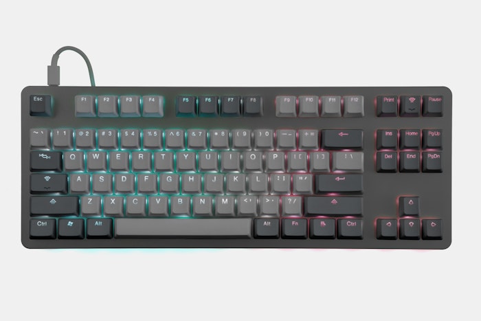 + +The Massdrop CTRL is a TKL mechanical keyboard featuring dual USB-C connectors, an integrated Hi-Speed USB 2.0 hub, and fully customizable RGB backlighting and underlighting. + +Keyboard Maintainer: [Massdrop](https://github.com/massdrop) +Hardware Supported: Massdrop, Inc. CTRL PCBs utilizing Microchip's ATSAMD51J18A MCU and USB2422 2-Port USB 2.0 Hi-Speed Hub Controller, and ISSI's IS31FL3733 LED Drivers. +Hardware Availability: [Massdrop CTRL Mechanical Keyboard](https://www.massdrop.com/buy/massdrop-ctrl-mechanical-keyboard) + +Make example for this keyboard (after setting up your build environment): + + make ctrl:default + +See the [build environment setup](https://docs.qmk.fm/#/getting_started_build_tools) and the [make instructions](https://docs.qmk.fm/#/getting_started_make_guide) for more information. Brand new to QMK? Start with our [Complete Newbs Guide](https://docs.qmk.fm/#/newbs).
\ No newline at end of file diff --git a/keyboards/ctrl/rules.mk b/keyboards/ctrl/rules.mk new file mode 100644 index 0000000000..daf6795852 --- /dev/null +++ b/keyboards/ctrl/rules.mk @@ -0,0 +1,32 @@ +# project specific files +SRC = led_programs.c +SRC += matrix.c + +#For platform and packs +ARM_ATSAM = SAMD51J18A +MCU = cortex-m4 + +CUSTOM_MATRIX = yes + +# Build Options +# comment out to disable the options. +# +BOOTMAGIC_ENABLE = no # Virtual DIP switch configuration(+1000) +MOUSEKEY_ENABLE = no # Mouse keys(+4700) +EXTRAKEY_ENABLE = yes # Audio control and System control(+450) +CONSOLE_ENABLE = no # Console for debug(+400) +COMMAND_ENABLE = no # Commands for debug and configuration +# Do not enable SLEEP_LED_ENABLE. it uses the same timer as BACKLIGHT_ENABLE +SLEEP_LED_ENABLE = no # Breathing sleep LED during USB suspend +# if this doesn't work, see here: https://github.com/tmk/tmk_keyboard/wiki/FAQ#nkro-doesnt-work +NKRO_ENABLE = yes # USB Nkey Rollover +BACKLIGHT_ENABLE = no # Enable keyboard backlight functionality on B7 by default +RGBLIGHT_ENABLE = no # Enable keyboard RGB underglow +MIDI_ENABLE = no # MIDI support (+2400 to 4200, depending on config) +UNICODE_ENABLE = no # Unicode +BLUETOOTH_ENABLE = no # Enable Bluetooth with the Adafruit EZ-Key HID +AUDIO_ENABLE = no # Audio output on port C6 +FAUXCLICKY_ENABLE = no # Use buzzer to emulate clicky switches +HD44780_ENABLE = no # Enable support for HD44780 based LCDs (+400) +VIRTSER_ENABLE = no # USB Serial Driver +RAW_ENABLE = no # Raw device diff --git a/lib/arm_atsam/packs/arm/cmsis/5.0.1/CMSIS/Include/arm_math.h b/lib/arm_atsam/packs/arm/cmsis/5.0.1/CMSIS/Include/arm_math.h new file mode 100644 index 0000000000..4be7e8c848 --- /dev/null +++ b/lib/arm_atsam/packs/arm/cmsis/5.0.1/CMSIS/Include/arm_math.h @@ -0,0 +1,7226 @@ +/* ---------------------------------------------------------------------- + * Project: CMSIS DSP Library + * Title: arm_math.h + * Description: Public header file for CMSIS DSP Library + * + * $Date: 27. January 2017 + * $Revision: V.1.5.1 + * + * Target Processor: Cortex-M cores + * -------------------------------------------------------------------- */ +/* + * Copyright (C) 2010-2017 ARM Limited or its affiliates. All rights reserved. + * + * SPDX-License-Identifier: Apache-2.0 + * + * Licensed under the Apache License, Version 2.0 (the License); you may + * not use this file except in compliance with the License. + * You may obtain a copy of the License at + * + * www.apache.org/licenses/LICENSE-2.0 + * + * Unless required by applicable law or agreed to in writing, software + * distributed under the License is distributed on an AS IS BASIS, WITHOUT + * WARRANTIES OR CONDITIONS OF ANY KIND, either express or implied. + * See the License for the specific language governing permissions and + * limitations under the License. + */ + +/** + \mainpage CMSIS DSP Software Library + * + * Introduction + * ------------ + * + * This user manual describes the CMSIS DSP software library, + * a suite of common signal processing functions for use on Cortex-M processor based devices. + * + * The library is divided into a number of functions each covering a specific category: + * - Basic math functions + * - Fast math functions + * - Complex math functions + * - Filters + * - Matrix functions + * - Transforms + * - Motor control functions + * - Statistical functions + * - Support functions + * - Interpolation functions + * + * The library has separate functions for operating on 8-bit integers, 16-bit integers, + * 32-bit integer and 32-bit floating-point values. + * + * Using the Library + * ------------ + * + * The library installer contains prebuilt versions of the libraries in the <code>Lib</code> folder. + * - arm_cortexM7lfdp_math.lib (Cortex-M7, Little endian, Double Precision Floating Point Unit) + * - arm_cortexM7bfdp_math.lib (Cortex-M7, Big endian, Double Precision Floating Point Unit) + * - arm_cortexM7lfsp_math.lib (Cortex-M7, Little endian, Single Precision Floating Point Unit) + * - arm_cortexM7bfsp_math.lib (Cortex-M7, Big endian and Single Precision Floating Point Unit on) + * - arm_cortexM7l_math.lib (Cortex-M7, Little endian) + * - arm_cortexM7b_math.lib (Cortex-M7, Big endian) + * - arm_cortexM4lf_math.lib (Cortex-M4, Little endian, Floating Point Unit) + * - arm_cortexM4bf_math.lib (Cortex-M4, Big endian, Floating Point Unit) + * - arm_cortexM4l_math.lib (Cortex-M4, Little endian) + * - arm_cortexM4b_math.lib (Cortex-M4, Big endian) + * - arm_cortexM3l_math.lib (Cortex-M3, Little endian) + * - arm_cortexM3b_math.lib (Cortex-M3, Big endian) + * - arm_cortexM0l_math.lib (Cortex-M0 / Cortex-M0+, Little endian) + * - arm_cortexM0b_math.lib (Cortex-M0 / Cortex-M0+, Big endian) + * - arm_ARMv8MBLl_math.lib (ARMv8M Baseline, Little endian) + * - arm_ARMv8MMLl_math.lib (ARMv8M Mainline, Little endian) + * - arm_ARMv8MMLlfsp_math.lib (ARMv8M Mainline, Little endian, Single Precision Floating Point Unit) + * - arm_ARMv8MMLld_math.lib (ARMv8M Mainline, Little endian, DSP instructions) + * - arm_ARMv8MMLldfsp_math.lib (ARMv8M Mainline, Little endian, DSP instructions, Single Precision Floating Point Unit) + * + * The library functions are declared in the public file <code>arm_math.h</code> which is placed in the <code>Include</code> folder. + * Simply include this file and link the appropriate library in the application and begin calling the library functions. The Library supports single + * public header file <code> arm_math.h</code> for Cortex-M cores with little endian and big endian. Same header file will be used for floating point unit(FPU) variants. + * Define the appropriate pre processor MACRO ARM_MATH_CM7 or ARM_MATH_CM4 or ARM_MATH_CM3 or + * ARM_MATH_CM0 or ARM_MATH_CM0PLUS depending on the target processor in the application. + * For ARMv8M cores define pre processor MACRO ARM_MATH_ARMV8MBL or ARM_MATH_ARMV8MML. + * Set Pre processor MACRO __DSP_PRESENT if ARMv8M Mainline core supports DSP instructions. + * + * + * Examples + * -------- + * + * The library ships with a number of examples which demonstrate how to use the library functions. + * + * Toolchain Support + * ------------ + * + * The library has been developed and tested with MDK-ARM version 5.14.0.0 + * The library is being tested in GCC and IAR toolchains and updates on this activity will be made available shortly. + * + * Building the Library + * ------------ + * + * The library installer contains a project file to re build libraries on MDK-ARM Tool chain in the <code>CMSIS\\DSP_Lib\\Source\\ARM</code> folder. + * - arm_cortexM_math.uvprojx + * + * + * The libraries can be built by opening the arm_cortexM_math.uvprojx project in MDK-ARM, selecting a specific target, and defining the optional pre processor MACROs detailed above. + * + * Pre-processor Macros + * ------------ + * + * Each library project have differant pre-processor macros. + * + * - UNALIGNED_SUPPORT_DISABLE: + * + * Define macro UNALIGNED_SUPPORT_DISABLE, If the silicon does not support unaligned memory access + * + * - ARM_MATH_BIG_ENDIAN: + * + * Define macro ARM_MATH_BIG_ENDIAN to build the library for big endian targets. By default library builds for little endian targets. + * + * - ARM_MATH_MATRIX_CHECK: + * + * Define macro ARM_MATH_MATRIX_CHECK for checking on the input and output sizes of matrices + * + * - ARM_MATH_ROUNDING: + * + * Define macro ARM_MATH_ROUNDING for rounding on support functions + * + * - ARM_MATH_CMx: + * + * Define macro ARM_MATH_CM4 for building the library on Cortex-M4 target, ARM_MATH_CM3 for building library on Cortex-M3 target + * and ARM_MATH_CM0 for building library on Cortex-M0 target, ARM_MATH_CM0PLUS for building library on Cortex-M0+ target, and + * ARM_MATH_CM7 for building the library on cortex-M7. + * + * - ARM_MATH_ARMV8MxL: + * + * Define macro ARM_MATH_ARMV8MBL for building the library on ARMv8M Baseline target, ARM_MATH_ARMV8MBL for building library + * on ARMv8M Mainline target. + * + * - __FPU_PRESENT: + * + * Initialize macro __FPU_PRESENT = 1 when building on FPU supported Targets. Enable this macro for floating point libraries. + * + * - __DSP_PRESENT: + * + * Initialize macro __DSP_PRESENT = 1 when ARMv8M Mainline core supports DSP instructions. + * + * <hr> + * CMSIS-DSP in ARM::CMSIS Pack + * ----------------------------- + * + * The following files relevant to CMSIS-DSP are present in the <b>ARM::CMSIS</b> Pack directories: + * |File/Folder |Content | + * |------------------------------|------------------------------------------------------------------------| + * |\b CMSIS\\Documentation\\DSP | This documentation | + * |\b CMSIS\\DSP_Lib | Software license agreement (license.txt) | + * |\b CMSIS\\DSP_Lib\\Examples | Example projects demonstrating the usage of the library functions | + * |\b CMSIS\\DSP_Lib\\Source | Source files for rebuilding the library | + * + * <hr> + * Revision History of CMSIS-DSP + * ------------ + * Please refer to \ref ChangeLog_pg. + * + * Copyright Notice + * ------------ + * + * Copyright (C) 2010-2015 ARM Limited. All rights reserved. + */ + + +/** + * @defgroup groupMath Basic Math Functions + */ + +/** + * @defgroup groupFastMath Fast Math Functions + * This set of functions provides a fast approximation to sine, cosine, and square root. + * As compared to most of the other functions in the CMSIS math library, the fast math functions + * operate on individual values and not arrays. + * There are separate functions for Q15, Q31, and floating-point data. + * + */ + +/** + * @defgroup groupCmplxMath Complex Math Functions + * This set of functions operates on complex data vectors. + * The data in the complex arrays is stored in an interleaved fashion + * (real, imag, real, imag, ...). + * In the API functions, the number of samples in a complex array refers + * to the number of complex values; the array contains twice this number of + * real values. + */ + +/** + * @defgroup groupFilters Filtering Functions + */ + +/** + * @defgroup groupMatrix Matrix Functions + * + * This set of functions provides basic matrix math operations. + * The functions operate on matrix data structures. For example, + * the type + * definition for the floating-point matrix structure is shown + * below: + * <pre> + * typedef struct + * { + * uint16_t numRows; // number of rows of the matrix. + * uint16_t numCols; // number of columns of the matrix. + * float32_t *pData; // points to the data of the matrix. + * } arm_matrix_instance_f32; + * </pre> + * There are similar definitions for Q15 and Q31 data types. + * + * The structure specifies the size of the matrix and then points to + * an array of data. The array is of size <code>numRows X numCols</code> + * and the values are arranged in row order. That is, the + * matrix element (i, j) is stored at: + * <pre> + * pData[i*numCols + j] + * </pre> + * + * \par Init Functions + * There is an associated initialization function for each type of matrix + * data structure. + * The initialization function sets the values of the internal structure fields. + * Refer to the function <code>arm_mat_init_f32()</code>, <code>arm_mat_init_q31()</code> + * and <code>arm_mat_init_q15()</code> for floating-point, Q31 and Q15 types, respectively. + * + * \par + * Use of the initialization function is optional. However, if initialization function is used + * then the instance structure cannot be placed into a const data section. + * To place the instance structure in a const data + * section, manually initialize the data structure. For example: + * <pre> + * <code>arm_matrix_instance_f32 S = {nRows, nColumns, pData};</code> + * <code>arm_matrix_instance_q31 S = {nRows, nColumns, pData};</code> + * <code>arm_matrix_instance_q15 S = {nRows, nColumns, pData};</code> + * </pre> + * where <code>nRows</code> specifies the number of rows, <code>nColumns</code> + * specifies the number of columns, and <code>pData</code> points to the + * data array. + * + * \par Size Checking + * By default all of the matrix functions perform size checking on the input and + * output matrices. For example, the matrix addition function verifies that the + * two input matrices and the output matrix all have the same number of rows and + * columns. If the size check fails the functions return: + * <pre> + * ARM_MATH_SIZE_MISMATCH + * </pre> + * Otherwise the functions return + * <pre> + * ARM_MATH_SUCCESS + * </pre> + * There is some overhead associated with this matrix size checking. + * The matrix size checking is enabled via the \#define + * <pre> + * ARM_MATH_MATRIX_CHECK + * </pre> + * within the library project settings. By default this macro is defined + * and size checking is enabled. By changing the project settings and + * undefining this macro size checking is eliminated and the functions + * run a bit faster. With size checking disabled the functions always + * return <code>ARM_MATH_SUCCESS</code>. + */ + +/** + * @defgroup groupTransforms Transform Functions + */ + +/** + * @defgroup groupController Controller Functions + */ + +/** + * @defgroup groupStats Statistics Functions + */ +/** + * @defgroup groupSupport Support Functions + */ + +/** + * @defgroup groupInterpolation Interpolation Functions + * These functions perform 1- and 2-dimensional interpolation of data. + * Linear interpolation is used for 1-dimensional data and + * bilinear interpolation is used for 2-dimensional data. + */ + +/** + * @defgroup groupExamples Examples + */ +#ifndef _ARM_MATH_H +#define _ARM_MATH_H + +/* ignore some GCC warnings */ +#if defined ( __GNUC__ ) +#pragma GCC diagnostic push +#pragma GCC diagnostic ignored "-Wsign-conversion" +#pragma GCC diagnostic ignored "-Wconversion" +#pragma GCC diagnostic ignored "-Wunused-parameter" +#endif + +#define __CMSIS_GENERIC /* disable NVIC and Systick functions */ + +#if defined(ARM_MATH_CM7) + #include "core_cm7.h" + #define ARM_MATH_DSP +#elif defined (ARM_MATH_CM4) + #include "core_cm4.h" + #define ARM_MATH_DSP +#elif defined (ARM_MATH_CM3) + #include "core_cm3.h" +#elif defined (ARM_MATH_CM0) + #include "core_cm0.h" + #define ARM_MATH_CM0_FAMILY +#elif defined (ARM_MATH_CM0PLUS) + #include "core_cm0plus.h" + #define ARM_MATH_CM0_FAMILY +#elif defined (ARM_MATH_ARMV8MBL) + #include "core_armv8mbl.h" + #define ARM_MATH_CM0_FAMILY +#elif defined (ARM_MATH_ARMV8MML) + #include "core_armv8mml.h" + #if (defined (__DSP_PRESENT) && (__DSP_PRESENT == 1)) + #define ARM_MATH_DSP + #endif +#else + #error "Define according the used Cortex core ARM_MATH_CM7, ARM_MATH_CM4, ARM_MATH_CM3, ARM_MATH_CM0PLUS, ARM_MATH_CM0, ARM_MATH_ARMV8MBL, ARM_MATH_ARMV8MML" +#endif + +#undef __CMSIS_GENERIC /* enable NVIC and Systick functions */ +#include "string.h" +#include "math.h" +#ifdef __cplusplus +extern "C" +{ +#endif + + + /** + * @brief Macros required for reciprocal calculation in Normalized LMS + */ + +#define DELTA_Q31 (0x100) +#define DELTA_Q15 0x5 +#define INDEX_MASK 0x0000003F +#ifndef PI + #define PI 3.14159265358979f +#endif + + /** + * @brief Macros required for SINE and COSINE Fast math approximations + */ + +#define FAST_MATH_TABLE_SIZE 512 +#define FAST_MATH_Q31_SHIFT (32 - 10) +#define FAST_MATH_Q15_SHIFT (16 - 10) +#define CONTROLLER_Q31_SHIFT (32 - 9) +#define TABLE_SPACING_Q31 0x400000 +#define TABLE_SPACING_Q15 0x80 + + /** + * @brief Macros required for SINE and COSINE Controller functions + */ + /* 1.31(q31) Fixed value of 2/360 */ + /* -1 to +1 is divided into 360 values so total spacing is (2/360) */ +#define INPUT_SPACING 0xB60B61 + + /** + * @brief Macro for Unaligned Support + */ +#ifndef UNALIGNED_SUPPORT_DISABLE + #define ALIGN4 +#else + #if defined (__GNUC__) + #define ALIGN4 __attribute__((aligned(4))) + #else + #define ALIGN4 __align(4) + #endif +#endif /* #ifndef UNALIGNED_SUPPORT_DISABLE */ + + /** + * @brief Error status returned by some functions in the library. + */ + + typedef enum + { + ARM_MATH_SUCCESS = 0, /**< No error */ + ARM_MATH_ARGUMENT_ERROR = -1, /**< One or more arguments are incorrect */ + ARM_MATH_LENGTH_ERROR = -2, /**< Length of data buffer is incorrect */ + ARM_MATH_SIZE_MISMATCH = -3, /**< Size of matrices is not compatible with the operation. */ + ARM_MATH_NANINF = -4, /**< Not-a-number (NaN) or infinity is generated */ + ARM_MATH_SINGULAR = -5, /**< Generated by matrix inversion if the input matrix is singular and cannot be inverted. */ + ARM_MATH_TEST_FAILURE = -6 /**< Test Failed */ + } arm_status; + + /** + * @brief 8-bit fractional data type in 1.7 format. + */ + typedef int8_t q7_t; + + /** + * @brief 16-bit fractional data type in 1.15 format. + */ + typedef int16_t q15_t; + + /** + * @brief 32-bit fractional data type in 1.31 format. + */ + typedef int32_t q31_t; + + /** + * @brief 64-bit fractional data type in 1.63 format. + */ + typedef int64_t q63_t; + + /** + * @brief 32-bit floating-point type definition. + */ + typedef float float32_t; + + /** + * @brief 64-bit floating-point type definition. + */ + typedef double float64_t; + + /** + * @brief definition to read/write two 16 bit values. + */ +#if defined ( __CC_ARM ) + #define __SIMD32_TYPE int32_t __packed + #define CMSIS_UNUSED __attribute__((unused)) + #define CMSIS_INLINE __attribute__((always_inline)) + +#elif defined ( __ARMCC_VERSION ) && ( __ARMCC_VERSION >= 6010050 ) + #define __SIMD32_TYPE int32_t + #define CMSIS_UNUSED __attribute__((unused)) + #define CMSIS_INLINE __attribute__((always_inline)) + +#elif defined ( __GNUC__ ) + #define __SIMD32_TYPE int32_t + #define CMSIS_UNUSED __attribute__((unused)) + #define CMSIS_INLINE __attribute__((always_inline)) + +#elif defined ( __ICCARM__ ) + #define __SIMD32_TYPE int32_t __packed + #define CMSIS_UNUSED + #define CMSIS_INLINE + +#elif defined ( __TI_ARM__ ) + #define __SIMD32_TYPE int32_t + #define CMSIS_UNUSED __attribute__((unused)) + #define CMSIS_INLINE + +#elif defined ( __CSMC__ ) + #define __SIMD32_TYPE int32_t + #define CMSIS_UNUSED + #define CMSIS_INLINE + +#elif defined ( __TASKING__ ) + #define __SIMD32_TYPE __unaligned int32_t + #define CMSIS_UNUSED + #define CMSIS_INLINE + +#else + #error Unknown compiler +#endif + +#define __SIMD32(addr) (*(__SIMD32_TYPE **) & (addr)) +#define __SIMD32_CONST(addr) ((__SIMD32_TYPE *)(addr)) +#define _SIMD32_OFFSET(addr) (*(__SIMD32_TYPE *) (addr)) +#define __SIMD64(addr) (*(int64_t **) & (addr)) + +/* #if defined (ARM_MATH_CM3) || defined (ARM_MATH_CM0_FAMILY) */ +#if !defined (ARM_MATH_DSP) + /** + * @brief definition to pack two 16 bit values. + */ +#define __PKHBT(ARG1, ARG2, ARG3) ( (((int32_t)(ARG1) << 0) & (int32_t)0x0000FFFF) | \ + (((int32_t)(ARG2) << ARG3) & (int32_t)0xFFFF0000) ) +#define __PKHTB(ARG1, ARG2, ARG3) ( (((int32_t)(ARG1) << 0) & (int32_t)0xFFFF0000) | \ + (((int32_t)(ARG2) >> ARG3) & (int32_t)0x0000FFFF) ) + +/* #endif // defined (ARM_MATH_CM3) || defined (ARM_MATH_CM0_FAMILY) */ +#endif /* !defined (ARM_MATH_DSP) */ + + /** + * @brief definition to pack four 8 bit values. + */ +#ifndef ARM_MATH_BIG_ENDIAN + +#define __PACKq7(v0,v1,v2,v3) ( (((int32_t)(v0) << 0) & (int32_t)0x000000FF) | \ + (((int32_t)(v1) << 8) & (int32_t)0x0000FF00) | \ + (((int32_t)(v2) << 16) & (int32_t)0x00FF0000) | \ + (((int32_t)(v3) << 24) & (int32_t)0xFF000000) ) +#else + +#define __PACKq7(v0,v1,v2,v3) ( (((int32_t)(v3) << 0) & (int32_t)0x000000FF) | \ + (((int32_t)(v2) << 8) & (int32_t)0x0000FF00) | \ + (((int32_t)(v1) << 16) & (int32_t)0x00FF0000) | \ + (((int32_t)(v0) << 24) & (int32_t)0xFF000000) ) + +#endif + + + /** + * @brief Clips Q63 to Q31 values. + */ + CMSIS_INLINE __STATIC_INLINE q31_t clip_q63_to_q31( + q63_t x) + { + return ((q31_t) (x >> 32) != ((q31_t) x >> 31)) ? + ((0x7FFFFFFF ^ ((q31_t) (x >> 63)))) : (q31_t) x; + } + + /** + * @brief Clips Q63 to Q15 values. + */ + CMSIS_INLINE __STATIC_INLINE q15_t clip_q63_to_q15( + q63_t x) + { + return ((q31_t) (x >> 32) != ((q31_t) x >> 31)) ? + ((0x7FFF ^ ((q15_t) (x >> 63)))) : (q15_t) (x >> 15); + } + + /** + * @brief Clips Q31 to Q7 values. + */ + CMSIS_INLINE __STATIC_INLINE q7_t clip_q31_to_q7( + q31_t x) + { + return ((q31_t) (x >> 24) != ((q31_t) x >> 23)) ? + ((0x7F ^ ((q7_t) (x >> 31)))) : (q7_t) x; + } + + /** + * @brief Clips Q31 to Q15 values. + */ + CMSIS_INLINE __STATIC_INLINE q15_t clip_q31_to_q15( + q31_t x) + { + return ((q31_t) (x >> 16) != ((q31_t) x >> 15)) ? + ((0x7FFF ^ ((q15_t) (x >> 31)))) : (q15_t) x; + } + + /** + * @brief Multiplies 32 X 64 and returns 32 bit result in 2.30 format. + */ + + CMSIS_INLINE __STATIC_INLINE q63_t mult32x64( + q63_t x, + q31_t y) + { + return ((((q63_t) (x & 0x00000000FFFFFFFF) * y) >> 32) + + (((q63_t) (x >> 32) * y))); + } + +/* + #if defined (ARM_MATH_CM0_FAMILY) && defined ( __CC_ARM ) + #define __CLZ __clz + #endif + */ +/* note: function can be removed when all toolchain support __CLZ for Cortex-M0 */ +#if defined (ARM_MATH_CM0_FAMILY) && ((defined (__ICCARM__)) ) + CMSIS_INLINE __STATIC_INLINE uint32_t __CLZ( + q31_t data); + + CMSIS_INLINE __STATIC_INLINE uint32_t __CLZ( + q31_t data) + { + uint32_t count = 0; + uint32_t mask = 0x80000000; + + while ((data & mask) == 0) + { + count += 1u; + mask = mask >> 1u; + } + + return (count); + } +#endif + + /** + * @brief Function to Calculates 1/in (reciprocal) value of Q31 Data type. + */ + + CMSIS_INLINE __STATIC_INLINE uint32_t arm_recip_q31( + q31_t in, + q31_t * dst, + q31_t * pRecipTable) + { + q31_t out; + uint32_t tempVal; + uint32_t index, i; + uint32_t signBits; + + if (in > 0) + { + signBits = ((uint32_t) (__CLZ( in) - 1)); + } + else + { + signBits = ((uint32_t) (__CLZ(-in) - 1)); + } + + /* Convert input sample to 1.31 format */ + in = (in << signBits); + + /* calculation of index for initial approximated Val */ + index = (uint32_t)(in >> 24); + index = (index & INDEX_MASK); + + /* 1.31 with exp 1 */ + out = pRecipTable[index]; + + /* calculation of reciprocal value */ + /* running approximation for two iterations */ + for (i = 0u; i < 2u; i++) + { + tempVal = (uint32_t) (((q63_t) in * out) >> 31); + tempVal = 0x7FFFFFFFu - tempVal; + /* 1.31 with exp 1 */ + /* out = (q31_t) (((q63_t) out * tempVal) >> 30); */ + out = clip_q63_to_q31(((q63_t) out * tempVal) >> 30); + } + + /* write output */ + *dst = out; + + /* return num of signbits of out = 1/in value */ + return (signBits + 1u); + } + + + /** + * @brief Function to Calculates 1/in (reciprocal) value of Q15 Data type. + */ + CMSIS_INLINE __STATIC_INLINE uint32_t arm_recip_q15( + q15_t in, + q15_t * dst, + q15_t * pRecipTable) + { + q15_t out = 0; + uint32_t tempVal = 0; + uint32_t index = 0, i = 0; + uint32_t signBits = 0; + + if (in > 0) + { + signBits = ((uint32_t)(__CLZ( in) - 17)); + } + else + { + signBits = ((uint32_t)(__CLZ(-in) - 17)); + } + + /* Convert input sample to 1.15 format */ + in = (in << signBits); + + /* calculation of index for initial approximated Val */ + index = (uint32_t)(in >> 8); + index = (index & INDEX_MASK); + + /* 1.15 with exp 1 */ + out = pRecipTable[index]; + + /* calculation of reciprocal value */ + /* running approximation for two iterations */ + for (i = 0u; i < 2u; i++) + { + tempVal = (uint32_t) (((q31_t) in * out) >> 15); + tempVal = 0x7FFFu - tempVal; + /* 1.15 with exp 1 */ + out = (q15_t) (((q31_t) out * tempVal) >> 14); + /* out = clip_q31_to_q15(((q31_t) out * tempVal) >> 14); */ + } + + /* write output */ + *dst = out; + + /* return num of signbits of out = 1/in value */ + return (signBits + 1); + } + + + /* + * @brief C custom defined intrinisic function for only M0 processors + */ +#if defined(ARM_MATH_CM0_FAMILY) + CMSIS_INLINE __STATIC_INLINE q31_t __SSAT( + q31_t x, + uint32_t y) + { + int32_t posMax, negMin; + uint32_t i; + + posMax = 1; + for (i = 0; i < (y - 1); i++) + { + posMax = posMax * 2; + } + + if (x > 0) + { + posMax = (posMax - 1); + + if (x > posMax) + { + x = posMax; + } + } + else + { + negMin = -posMax; + + if (x < negMin) + { + x = negMin; + } + } + return (x); + } +#endif /* end of ARM_MATH_CM0_FAMILY */ + + + /* + * @brief C custom defined intrinsic function for M3 and M0 processors + */ +/* #if defined (ARM_MATH_CM3) || defined (ARM_MATH_CM0_FAMILY) */ +#if !defined (ARM_MATH_DSP) + + /* + * @brief C custom defined QADD8 for M3 and M0 processors + */ + CMSIS_INLINE __STATIC_INLINE uint32_t __QADD8( + uint32_t x, + uint32_t y) + { + q31_t r, s, t, u; + + r = __SSAT(((((q31_t)x << 24) >> 24) + (((q31_t)y << 24) >> 24)), 8) & (int32_t)0x000000FF; + s = __SSAT(((((q31_t)x << 16) >> 24) + (((q31_t)y << 16) >> 24)), 8) & (int32_t)0x000000FF; + t = __SSAT(((((q31_t)x << 8) >> 24) + (((q31_t)y << 8) >> 24)), 8) & (int32_t)0x000000FF; + u = __SSAT(((((q31_t)x ) >> 24) + (((q31_t)y ) >> 24)), 8) & (int32_t)0x000000FF; + + return ((uint32_t)((u << 24) | (t << 16) | (s << 8) | (r ))); + } + + + /* + * @brief C custom defined QSUB8 for M3 and M0 processors + */ + CMSIS_INLINE __STATIC_INLINE uint32_t __QSUB8( + uint32_t x, + uint32_t y) + { + q31_t r, s, t, u; + + r = __SSAT(((((q31_t)x << 24) >> 24) - (((q31_t)y << 24) >> 24)), 8) & (int32_t)0x000000FF; + s = __SSAT(((((q31_t)x << 16) >> 24) - (((q31_t)y << 16) >> 24)), 8) & (int32_t)0x000000FF; + t = __SSAT(((((q31_t)x << 8) >> 24) - (((q31_t)y << 8) >> 24)), 8) & (int32_t)0x000000FF; + u = __SSAT(((((q31_t)x ) >> 24) - (((q31_t)y ) >> 24)), 8) & (int32_t)0x000000FF; + + return ((uint32_t)((u << 24) | (t << 16) | (s << 8) | (r ))); + } + + + /* + * @brief C custom defined QADD16 for M3 and M0 processors + */ + CMSIS_INLINE __STATIC_INLINE uint32_t __QADD16( + uint32_t x, + uint32_t y) + { +/* q31_t r, s; without initialisation 'arm_offset_q15 test' fails but 'intrinsic' tests pass! for armCC */ + q31_t r = 0, s = 0; + + r = __SSAT(((((q31_t)x << 16) >> 16) + (((q31_t)y << 16) >> 16)), 16) & (int32_t)0x0000FFFF; + s = __SSAT(((((q31_t)x ) >> 16) + (((q31_t)y ) >> 16)), 16) & (int32_t)0x0000FFFF; + + return ((uint32_t)((s << 16) | (r ))); + } + + + /* + * @brief C custom defined SHADD16 for M3 and M0 processors + */ + CMSIS_INLINE __STATIC_INLINE uint32_t __SHADD16( + uint32_t x, + uint32_t y) + { + q31_t r, s; + + r = (((((q31_t)x << 16) >> 16) + (((q31_t)y << 16) >> 16)) >> 1) & (int32_t)0x0000FFFF; + s = (((((q31_t)x ) >> 16) + (((q31_t)y ) >> 16)) >> 1) & (int32_t)0x0000FFFF; + + return ((uint32_t)((s << 16) | (r ))); + } + + + /* + * @brief C custom defined QSUB16 for M3 and M0 processors + */ + CMSIS_INLINE __STATIC_INLINE uint32_t __QSUB16( + uint32_t x, + uint32_t y) + { + q31_t r, s; + + r = __SSAT(((((q31_t)x << 16) >> 16) - (((q31_t)y << 16) >> 16)), 16) & (int32_t)0x0000FFFF; + s = __SSAT(((((q31_t)x ) >> 16) - (((q31_t)y ) >> 16)), 16) & (int32_t)0x0000FFFF; + + return ((uint32_t)((s << 16) | (r ))); + } + + + /* + * @brief C custom defined SHSUB16 for M3 and M0 processors + */ + CMSIS_INLINE __STATIC_INLINE uint32_t __SHSUB16( + uint32_t x, + uint32_t y) + { + q31_t r, s; + + r = (((((q31_t)x << 16) >> 16) - (((q31_t)y << 16) >> 16)) >> 1) & (int32_t)0x0000FFFF; + s = (((((q31_t)x ) >> 16) - (((q31_t)y ) >> 16)) >> 1) & (int32_t)0x0000FFFF; + + return ((uint32_t)((s << 16) | (r ))); + } + + + /* + * @brief C custom defined QASX for M3 and M0 processors + */ + CMSIS_INLINE __STATIC_INLINE uint32_t __QASX( + uint32_t x, + uint32_t y) + { + q31_t r, s; + + r = __SSAT(((((q31_t)x << 16) >> 16) - (((q31_t)y ) >> 16)), 16) & (int32_t)0x0000FFFF; + s = __SSAT(((((q31_t)x ) >> 16) + (((q31_t)y << 16) >> 16)), 16) & (int32_t)0x0000FFFF; + + return ((uint32_t)((s << 16) | (r ))); + } + + + /* + * @brief C custom defined SHASX for M3 and M0 processors + */ + CMSIS_INLINE __STATIC_INLINE uint32_t __SHASX( + uint32_t x, + uint32_t y) + { + q31_t r, s; + + r = (((((q31_t)x << 16) >> 16) - (((q31_t)y ) >> 16)) >> 1) & (int32_t)0x0000FFFF; + s = (((((q31_t)x ) >> 16) + (((q31_t)y << 16) >> 16)) >> 1) & (int32_t)0x0000FFFF; + + return ((uint32_t)((s << 16) | (r ))); + } + + + /* + * @brief C custom defined QSAX for M3 and M0 processors + */ + CMSIS_INLINE __STATIC_INLINE uint32_t __QSAX( + uint32_t x, + uint32_t y) + { + q31_t r, s; + + r = __SSAT(((((q31_t)x << 16) >> 16) + (((q31_t)y ) >> 16)), 16) & (int32_t)0x0000FFFF; + s = __SSAT(((((q31_t)x ) >> 16) - (((q31_t)y << 16) >> 16)), 16) & (int32_t)0x0000FFFF; + + return ((uint32_t)((s << 16) | (r ))); + } + + + /* + * @brief C custom defined SHSAX for M3 and M0 processors + */ + CMSIS_INLINE __STATIC_INLINE uint32_t __SHSAX( + uint32_t x, + uint32_t y) + { + q31_t r, s; + + r = (((((q31_t)x << 16) >> 16) + (((q31_t)y ) >> 16)) >> 1) & (int32_t)0x0000FFFF; + s = (((((q31_t)x ) >> 16) - (((q31_t)y << 16) >> 16)) >> 1) & (int32_t)0x0000FFFF; + + return ((uint32_t)((s << 16) | (r ))); + } + + + /* + * @brief C custom defined SMUSDX for M3 and M0 processors + */ + CMSIS_INLINE __STATIC_INLINE uint32_t __SMUSDX( + uint32_t x, + uint32_t y) + { + return ((uint32_t)(((((q31_t)x << 16) >> 16) * (((q31_t)y ) >> 16)) - + ((((q31_t)x ) >> 16) * (((q31_t)y << 16) >> 16)) )); + } + + /* + * @brief C custom defined SMUADX for M3 and M0 processors + */ + CMSIS_INLINE __STATIC_INLINE uint32_t __SMUADX( + uint32_t x, + uint32_t y) + { + return ((uint32_t)(((((q31_t)x << 16) >> 16) * (((q31_t)y ) >> 16)) + + ((((q31_t)x ) >> 16) * (((q31_t)y << 16) >> 16)) )); + } + + + /* + * @brief C custom defined QADD for M3 and M0 processors + */ + CMSIS_INLINE __STATIC_INLINE int32_t __QADD( + int32_t x, + int32_t y) + { + return ((int32_t)(clip_q63_to_q31((q63_t)x + (q31_t)y))); + } + + + /* + * @brief C custom defined QSUB for M3 and M0 processors + */ + CMSIS_INLINE __STATIC_INLINE int32_t __QSUB( + int32_t x, + int32_t y) + { + return ((int32_t)(clip_q63_to_q31((q63_t)x - (q31_t)y))); + } + + + /* + * @brief C custom defined SMLAD for M3 and M0 processors + */ + CMSIS_INLINE __STATIC_INLINE uint32_t __SMLAD( + uint32_t x, + uint32_t y, + uint32_t sum) + { + return ((uint32_t)(((((q31_t)x << 16) >> 16) * (((q31_t)y << 16) >> 16)) + + ((((q31_t)x ) >> 16) * (((q31_t)y ) >> 16)) + + ( ((q31_t)sum ) ) )); + } + + + /* + * @brief C custom defined SMLADX for M3 and M0 processors + */ + CMSIS_INLINE __STATIC_INLINE uint32_t __SMLADX( + uint32_t x, + uint32_t y, + uint32_t sum) + { + return ((uint32_t)(((((q31_t)x << 16) >> 16) * (((q31_t)y ) >> 16)) + + ((((q31_t)x ) >> 16) * (((q31_t)y << 16) >> 16)) + + ( ((q31_t)sum ) ) )); + } + + + /* + * @brief C custom defined SMLSDX for M3 and M0 processors + */ + CMSIS_INLINE __STATIC_INLINE uint32_t __SMLSDX( + uint32_t x, + uint32_t y, + uint32_t sum) + { + return ((uint32_t)(((((q31_t)x << 16) >> 16) * (((q31_t)y ) >> 16)) - + ((((q31_t)x ) >> 16) * (((q31_t)y << 16) >> 16)) + + ( ((q31_t)sum ) ) )); + } + + + /* + * @brief C custom defined SMLALD for M3 and M0 processors + */ + CMSIS_INLINE __STATIC_INLINE uint64_t __SMLALD( + uint32_t x, + uint32_t y, + uint64_t sum) + { +/* return (sum + ((q15_t) (x >> 16) * (q15_t) (y >> 16)) + ((q15_t) x * (q15_t) y)); */ + return ((uint64_t)(((((q31_t)x << 16) >> 16) * (((q31_t)y << 16) >> 16)) + + ((((q31_t)x ) >> 16) * (((q31_t)y ) >> 16)) + + ( ((q63_t)sum ) ) )); + } + + + /* + * @brief C custom defined SMLALDX for M3 and M0 processors + */ + CMSIS_INLINE __STATIC_INLINE uint64_t __SMLALDX( + uint32_t x, + uint32_t y, + uint64_t sum) + { +/* return (sum + ((q15_t) (x >> 16) * (q15_t) y)) + ((q15_t) x * (q15_t) (y >> 16)); */ + return ((uint64_t)(((((q31_t)x << 16) >> 16) * (((q31_t)y ) >> 16)) + + ((((q31_t)x ) >> 16) * (((q31_t)y << 16) >> 16)) + + ( ((q63_t)sum ) ) )); + } + + + /* + * @brief C custom defined SMUAD for M3 and M0 processors + */ + CMSIS_INLINE __STATIC_INLINE uint32_t __SMUAD( + uint32_t x, + uint32_t y) + { + return ((uint32_t)(((((q31_t)x << 16) >> 16) * (((q31_t)y << 16) >> 16)) + + ((((q31_t)x ) >> 16) * (((q31_t)y ) >> 16)) )); + } + + + /* + * @brief C custom defined SMUSD for M3 and M0 processors + */ + CMSIS_INLINE __STATIC_INLINE uint32_t __SMUSD( + uint32_t x, + uint32_t y) + { + return ((uint32_t)(((((q31_t)x << 16) >> 16) * (((q31_t)y << 16) >> 16)) - + ((((q31_t)x ) >> 16) * (((q31_t)y ) >> 16)) )); + } + + + /* + * @brief C custom defined SXTB16 for M3 and M0 processors + */ + CMSIS_INLINE __STATIC_INLINE uint32_t __SXTB16( + uint32_t x) + { + return ((uint32_t)(((((q31_t)x << 24) >> 24) & (q31_t)0x0000FFFF) | + ((((q31_t)x << 8) >> 8) & (q31_t)0xFFFF0000) )); + } + + /* + * @brief C custom defined SMMLA for M3 and M0 processors + */ + CMSIS_INLINE __STATIC_INLINE int32_t __SMMLA( + int32_t x, + int32_t y, + int32_t sum) + { + return (sum + (int32_t) (((int64_t) x * y) >> 32)); + } + +#if 0 + /* + * @brief C custom defined PKHBT for unavailable DSP extension + */ + CMSIS_INLINE __STATIC_INLINE uint32_t __PKHBT( + uint32_t x, + uint32_t y, + uint32_t leftshift) + { + return ( ((x ) & 0x0000FFFFUL) | + ((y << leftshift) & 0xFFFF0000UL) ); + } + + /* + * @brief C custom defined PKHTB for unavailable DSP extension + */ + CMSIS_INLINE __STATIC_INLINE uint32_t __PKHTB( + uint32_t x, + uint32_t y, + uint32_t rightshift) + { + return ( ((x ) & 0xFFFF0000UL) | + ((y >> rightshift) & 0x0000FFFFUL) ); + } +#endif + +/* #endif // defined (ARM_MATH_CM3) || defined (ARM_MATH_CM0_FAMILY) */ +#endif /* !defined (ARM_MATH_DSP) */ + + + /** + * @brief Instance structure for the Q7 FIR filter. + */ + typedef struct + { + uint16_t numTaps; /**< number of filter coefficients in the filter. */ + q7_t *pState; /**< points to the state variable array. The array is of length numTaps+blockSize-1. */ + q7_t *pCoeffs; /**< points to the coefficient array. The array is of length numTaps.*/ + } arm_fir_instance_q7; + + /** + * @brief Instance structure for the Q15 FIR filter. + */ + typedef struct + { + uint16_t numTaps; /**< number of filter coefficients in the filter. */ + q15_t *pState; /**< points to the state variable array. The array is of length numTaps+blockSize-1. */ + q15_t *pCoeffs; /**< points to the coefficient array. The array is of length numTaps.*/ + } arm_fir_instance_q15; + + /** + * @brief Instance structure for the Q31 FIR filter. + */ + typedef struct + { + uint16_t numTaps; /**< number of filter coefficients in the filter. */ + q31_t *pState; /**< points to the state variable array. The array is of length numTaps+blockSize-1. */ + q31_t *pCoeffs; /**< points to the coefficient array. The array is of length numTaps. */ + } arm_fir_instance_q31; + + /** + * @brief Instance structure for the floating-point FIR filter. + */ + typedef struct + { + uint16_t numTaps; /**< number of filter coefficients in the filter. */ + float32_t *pState; /**< points to the state variable array. The array is of length numTaps+blockSize-1. */ + float32_t *pCoeffs; /**< points to the coefficient array. The array is of length numTaps. */ + } arm_fir_instance_f32; + + + /** + * @brief Processing function for the Q7 FIR filter. + * @param[in] S points to an instance of the Q7 FIR filter structure. + * @param[in] pSrc points to the block of input data. + * @param[out] pDst points to the block of output data. + * @param[in] blockSize number of samples to process. + */ + void arm_fir_q7( + const arm_fir_instance_q7 * S, + q7_t * pSrc, + q7_t * pDst, + uint32_t blockSize); + + + /** + * @brief Initialization function for the Q7 FIR filter. + * @param[in,out] S points to an instance of the Q7 FIR structure. + * @param[in] numTaps Number of filter coefficients in the filter. + * @param[in] pCoeffs points to the filter coefficients. + * @param[in] pState points to the state buffer. + * @param[in] blockSize number of samples that are processed. + */ + void arm_fir_init_q7( + arm_fir_instance_q7 * S, + uint16_t numTaps, + q7_t * pCoeffs, + q7_t * pState, + uint32_t blockSize); + + + /** + * @brief Processing function for the Q15 FIR filter. + * @param[in] S points to an instance of the Q15 FIR structure. + * @param[in] pSrc points to the block of input data. + * @param[out] pDst points to the block of output data. + * @param[in] blockSize number of samples to process. + */ + void arm_fir_q15( + const arm_fir_instance_q15 * S, + q15_t * pSrc, + q15_t * pDst, + uint32_t blockSize); + + + /** + * @brief Processing function for the fast Q15 FIR filter for Cortex-M3 and Cortex-M4. + * @param[in] S points to an instance of the Q15 FIR filter structure. + * @param[in] pSrc points to the block of input data. + * @param[out] pDst points to the block of output data. + * @param[in] blockSize number of samples to process. + */ + void arm_fir_fast_q15( + const arm_fir_instance_q15 * S, + q15_t * pSrc, + q15_t * pDst, + uint32_t blockSize); + + + /** + * @brief Initialization function for the Q15 FIR filter. + * @param[in,out] S points to an instance of the Q15 FIR filter structure. + * @param[in] numTaps Number of filter coefficients in the filter. Must be even and greater than or equal to 4. + * @param[in] pCoeffs points to the filter coefficients. + * @param[in] pState points to the state buffer. + * @param[in] blockSize number of samples that are processed at a time. + * @return The function returns ARM_MATH_SUCCESS if initialization was successful or ARM_MATH_ARGUMENT_ERROR if + * <code>numTaps</code> is not a supported value. + */ + arm_status arm_fir_init_q15( + arm_fir_instance_q15 * S, + uint16_t numTaps, + q15_t * pCoeffs, + q15_t * pState, + uint32_t blockSize); + + + /** + * @brief Processing function for the Q31 FIR filter. + * @param[in] S points to an instance of the Q31 FIR filter structure. + * @param[in] pSrc points to the block of input data. + * @param[out] pDst points to the block of output data. + * @param[in] blockSize number of samples to process. + */ + void arm_fir_q31( + const arm_fir_instance_q31 * S, + q31_t * pSrc, + q31_t * pDst, + uint32_t blockSize); + + + /** + * @brief Processing function for the fast Q31 FIR filter for Cortex-M3 and Cortex-M4. + * @param[in] S points to an instance of the Q31 FIR structure. + * @param[in] pSrc points to the block of input data. + * @param[out] pDst points to the block of output data. + * @param[in] blockSize number of samples to process. + */ + void arm_fir_fast_q31( + const arm_fir_instance_q31 * S, + q31_t * pSrc, + q31_t * pDst, + uint32_t blockSize); + + + /** + * @brief Initialization function for the Q31 FIR filter. + * @param[in,out] S points to an instance of the Q31 FIR structure. + * @param[in] numTaps Number of filter coefficients in the filter. + * @param[in] pCoeffs points to the filter coefficients. + * @param[in] pState points to the state buffer. + * @param[in] blockSize number of samples that are processed at a time. + */ + void arm_fir_init_q31( + arm_fir_instance_q31 * S, + uint16_t numTaps, + q31_t * pCoeffs, + q31_t * pState, + uint32_t blockSize); + + + /** + * @brief Processing function for the floating-point FIR filter. + * @param[in] S points to an instance of the floating-point FIR structure. + * @param[in] pSrc points to the block of input data. + * @param[out] pDst points to the block of output data. + * @param[in] blockSize number of samples to process. + */ + void arm_fir_f32( + const arm_fir_instance_f32 * S, + float32_t * pSrc, + float32_t * pDst, + uint32_t blockSize); + + + /** + * @brief Initialization function for the floating-point FIR filter. + * @param[in,out] S points to an instance of the floating-point FIR filter structure. + * @param[in] numTaps Number of filter coefficients in the filter. + * @param[in] pCoeffs points to the filter coefficients. + * @param[in] pState points to the state buffer. + * @param[in] blockSize number of samples that are processed at a time. + */ + void arm_fir_init_f32( + arm_fir_instance_f32 * S, + uint16_t numTaps, + float32_t * pCoeffs, + float32_t * pState, + uint32_t blockSize); + + + /** + * @brief Instance structure for the Q15 Biquad cascade filter. + */ + typedef struct + { + int8_t numStages; /**< number of 2nd order stages in the filter. Overall order is 2*numStages. */ + q15_t *pState; /**< Points to the array of state coefficients. The array is of length 4*numStages. */ + q15_t *pCoeffs; /**< Points to the array of coefficients. The array is of length 5*numStages. */ + int8_t postShift; /**< Additional shift, in bits, applied to each output sample. */ + } arm_biquad_casd_df1_inst_q15; + + /** + * @brief Instance structure for the Q31 Biquad cascade filter. + */ + typedef struct + { + uint32_t numStages; /**< number of 2nd order stages in the filter. Overall order is 2*numStages. */ + q31_t *pState; /**< Points to the array of state coefficients. The array is of length 4*numStages. */ + q31_t *pCoeffs; /**< Points to the array of coefficients. The array is of length 5*numStages. */ + uint8_t postShift; /**< Additional shift, in bits, applied to each output sample. */ + } arm_biquad_casd_df1_inst_q31; + + /** + * @brief Instance structure for the floating-point Biquad cascade filter. + */ + typedef struct + { + uint32_t numStages; /**< number of 2nd order stages in the filter. Overall order is 2*numStages. */ + float32_t *pState; /**< Points to the array of state coefficients. The array is of length 4*numStages. */ + float32_t *pCoeffs; /**< Points to the array of coefficients. The array is of length 5*numStages. */ + } arm_biquad_casd_df1_inst_f32; + + + /** + * @brief Processing function for the Q15 Biquad cascade filter. + * @param[in] S points to an instance of the Q15 Biquad cascade structure. + * @param[in] pSrc points to the block of input data. + * @param[out] pDst points to the block of output data. + * @param[in] blockSize number of samples to process. + */ + void arm_biquad_cascade_df1_q15( + const arm_biquad_casd_df1_inst_q15 * S, + q15_t * pSrc, + q15_t * pDst, + uint32_t blockSize); + + + /** + * @brief Initialization function for the Q15 Biquad cascade filter. + * @param[in,out] S points to an instance of the Q15 Biquad cascade structure. + * @param[in] numStages number of 2nd order stages in the filter. + * @param[in] pCoeffs points to the filter coefficients. + * @param[in] pState points to the state buffer. + * @param[in] postShift Shift to be applied to the output. Varies according to the coefficients format + */ + void arm_biquad_cascade_df1_init_q15( + arm_biquad_casd_df1_inst_q15 * S, + uint8_t numStages, + q15_t * pCoeffs, + q15_t * pState, + int8_t postShift); + + + /** + * @brief Fast but less precise processing function for the Q15 Biquad cascade filter for Cortex-M3 and Cortex-M4. + * @param[in] S points to an instance of the Q15 Biquad cascade structure. + * @param[in] pSrc points to the block of input data. + * @param[out] pDst points to the block of output data. + * @param[in] blockSize number of samples to process. + */ + void arm_biquad_cascade_df1_fast_q15( + const arm_biquad_casd_df1_inst_q15 * S, + q15_t * pSrc, + q15_t * pDst, + uint32_t blockSize); + + + /** + * @brief Processing function for the Q31 Biquad cascade filter + * @param[in] S points to an instance of the Q31 Biquad cascade structure. + * @param[in] pSrc points to the block of input data. + * @param[out] pDst points to the block of output data. + * @param[in] blockSize number of samples to process. + */ + void arm_biquad_cascade_df1_q31( + const arm_biquad_casd_df1_inst_q31 * S, + q31_t * pSrc, + q31_t * pDst, + uint32_t blockSize); + + + /** + * @brief Fast but less precise processing function for the Q31 Biquad cascade filter for Cortex-M3 and Cortex-M4. + * @param[in] S points to an instance of the Q31 Biquad cascade structure. + * @param[in] pSrc points to the block of input data. + * @param[out] pDst points to the block of output data. + * @param[in] blockSize number of samples to process. + */ + void arm_biquad_cascade_df1_fast_q31( + const arm_biquad_casd_df1_inst_q31 * S, + q31_t * pSrc, + q31_t * pDst, + uint32_t blockSize); + + + /** + * @brief Initialization function for the Q31 Biquad cascade filter. + * @param[in,out] S points to an instance of the Q31 Biquad cascade structure. + * @param[in] numStages number of 2nd order stages in the filter. + * @param[in] pCoeffs points to the filter coefficients. + * @param[in] pState points to the state buffer. + * @param[in] postShift Shift to be applied to the output. Varies according to the coefficients format + */ + void arm_biquad_cascade_df1_init_q31( + arm_biquad_casd_df1_inst_q31 * S, + uint8_t numStages, + q31_t * pCoeffs, + q31_t * pState, + int8_t postShift); + + + /** + * @brief Processing function for the floating-point Biquad cascade filter. + * @param[in] S points to an instance of the floating-point Biquad cascade structure. + * @param[in] pSrc points to the block of input data. + * @param[out] pDst points to the block of output data. + * @param[in] blockSize number of samples to process. + */ + void arm_biquad_cascade_df1_f32( + const arm_biquad_casd_df1_inst_f32 * S, + float32_t * pSrc, + float32_t * pDst, + uint32_t blockSize); + + + /** + * @brief Initialization function for the floating-point Biquad cascade filter. + * @param[in,out] S points to an instance of the floating-point Biquad cascade structure. + * @param[in] numStages number of 2nd order stages in the filter. + * @param[in] pCoeffs points to the filter coefficients. + * @param[in] pState points to the state buffer. + */ + void arm_biquad_cascade_df1_init_f32( + arm_biquad_casd_df1_inst_f32 * S, + uint8_t numStages, + float32_t * pCoeffs, + float32_t * pState); + + + /** + * @brief Instance structure for the floating-point matrix structure. + */ + typedef struct + { + uint16_t numRows; /**< number of rows of the matrix. */ + uint16_t numCols; /**< number of columns of the matrix. */ + float32_t *pData; /**< points to the data of the matrix. */ + } arm_matrix_instance_f32; + + + /** + * @brief Instance structure for the floating-point matrix structure. + */ + typedef struct + { + uint16_t numRows; /**< number of rows of the matrix. */ + uint16_t numCols; /**< number of columns of the matrix. */ + float64_t *pData; /**< points to the data of the matrix. */ + } arm_matrix_instance_f64; + + /** + * @brief Instance structure for the Q15 matrix structure. + */ + typedef struct + { + uint16_t numRows; /**< number of rows of the matrix. */ + uint16_t numCols; /**< number of columns of the matrix. */ + q15_t *pData; /**< points to the data of the matrix. */ + } arm_matrix_instance_q15; + + /** + * @brief Instance structure for the Q31 matrix structure. + */ + typedef struct + { + uint16_t numRows; /**< number of rows of the matrix. */ + uint16_t numCols; /**< number of columns of the matrix. */ + q31_t *pData; /**< points to the data of the matrix. */ + } arm_matrix_instance_q31; + + + /** + * @brief Floating-point matrix addition. + * @param[in] pSrcA points to the first input matrix structure + * @param[in] pSrcB points to the second input matrix structure + * @param[out] pDst points to output matrix structure + * @return The function returns either + * <code>ARM_MATH_SIZE_MISMATCH</code> or <code>ARM_MATH_SUCCESS</code> based on the outcome of size checking. + */ + arm_status arm_mat_add_f32( + const arm_matrix_instance_f32 * pSrcA, + const arm_matrix_instance_f32 * pSrcB, + arm_matrix_instance_f32 * pDst); + + + /** + * @brief Q15 matrix addition. + * @param[in] pSrcA points to the first input matrix structure + * @param[in] pSrcB points to the second input matrix structure + * @param[out] pDst points to output matrix structure + * @return The function returns either + * <code>ARM_MATH_SIZE_MISMATCH</code> or <code>ARM_MATH_SUCCESS</code> based on the outcome of size checking. + */ + arm_status arm_mat_add_q15( + const arm_matrix_instance_q15 * pSrcA, + const arm_matrix_instance_q15 * pSrcB, + arm_matrix_instance_q15 * pDst); + + + /** + * @brief Q31 matrix addition. + * @param[in] pSrcA points to the first input matrix structure + * @param[in] pSrcB points to the second input matrix structure + * @param[out] pDst points to output matrix structure + * @return The function returns either + * <code>ARM_MATH_SIZE_MISMATCH</code> or <code>ARM_MATH_SUCCESS</code> based on the outcome of size checking. + */ + arm_status arm_mat_add_q31( + const arm_matrix_instance_q31 * pSrcA, + const arm_matrix_instance_q31 * pSrcB, + arm_matrix_instance_q31 * pDst); + + + /** + * @brief Floating-point, complex, matrix multiplication. + * @param[in] pSrcA points to the first input matrix structure + * @param[in] pSrcB points to the second input matrix structure + * @param[out] pDst points to output matrix structure + * @return The function returns either + * <code>ARM_MATH_SIZE_MISMATCH</code> or <code>ARM_MATH_SUCCESS</code> based on the outcome of size checking. + */ + arm_status arm_mat_cmplx_mult_f32( + const arm_matrix_instance_f32 * pSrcA, + const arm_matrix_instance_f32 * pSrcB, + arm_matrix_instance_f32 * pDst); + + + /** + * @brief Q15, complex, matrix multiplication. + * @param[in] pSrcA points to the first input matrix structure + * @param[in] pSrcB points to the second input matrix structure + * @param[out] pDst points to output matrix structure + * @return The function returns either + * <code>ARM_MATH_SIZE_MISMATCH</code> or <code>ARM_MATH_SUCCESS</code> based on the outcome of size checking. + */ + arm_status arm_mat_cmplx_mult_q15( + const arm_matrix_instance_q15 * pSrcA, + const arm_matrix_instance_q15 * pSrcB, + arm_matrix_instance_q15 * pDst, + q15_t * pScratch); + + + /** + * @brief Q31, complex, matrix multiplication. + * @param[in] pSrcA points to the first input matrix structure + * @param[in] pSrcB points to the second input matrix structure + * @param[out] pDst points to output matrix structure + * @return The function returns either + * <code>ARM_MATH_SIZE_MISMATCH</code> or <code>ARM_MATH_SUCCESS</code> based on the outcome of size checking. + */ + arm_status arm_mat_cmplx_mult_q31( + const arm_matrix_instance_q31 * pSrcA, + const arm_matrix_instance_q31 * pSrcB, + arm_matrix_instance_q31 * pDst); + + + /** + * @brief Floating-point matrix transpose. + * @param[in] pSrc points to the input matrix + * @param[out] pDst points to the output matrix + * @return The function returns either <code>ARM_MATH_SIZE_MISMATCH</code> + * or <code>ARM_MATH_SUCCESS</code> based on the outcome of size checking. + */ + arm_status arm_mat_trans_f32( + const arm_matrix_instance_f32 * pSrc, + arm_matrix_instance_f32 * pDst); + + + /** + * @brief Q15 matrix transpose. + * @param[in] pSrc points to the input matrix + * @param[out] pDst points to the output matrix + * @return The function returns either <code>ARM_MATH_SIZE_MISMATCH</code> + * or <code>ARM_MATH_SUCCESS</code> based on the outcome of size checking. + */ + arm_status arm_mat_trans_q15( + const arm_matrix_instance_q15 * pSrc, + arm_matrix_instance_q15 * pDst); + + + /** + * @brief Q31 matrix transpose. + * @param[in] pSrc points to the input matrix + * @param[out] pDst points to the output matrix + * @return The function returns either <code>ARM_MATH_SIZE_MISMATCH</code> + * or <code>ARM_MATH_SUCCESS</code> based on the outcome of size checking. + */ + arm_status arm_mat_trans_q31( + const arm_matrix_instance_q31 * pSrc, + arm_matrix_instance_q31 * pDst); + + + /** + * @brief Floating-point matrix multiplication + * @param[in] pSrcA points to the first input matrix structure + * @param[in] pSrcB points to the second input matrix structure + * @param[out] pDst points to output matrix structure + * @return The function returns either + * <code>ARM_MATH_SIZE_MISMATCH</code> or <code>ARM_MATH_SUCCESS</code> based on the outcome of size checking. + */ + arm_status arm_mat_mult_f32( + const arm_matrix_instance_f32 * pSrcA, + const arm_matrix_instance_f32 * pSrcB, + arm_matrix_instance_f32 * pDst); + + + /** + * @brief Q15 matrix multiplication + * @param[in] pSrcA points to the first input matrix structure + * @param[in] pSrcB points to the second input matrix structure + * @param[out] pDst points to output matrix structure + * @param[in] pState points to the array for storing intermediate results + * @return The function returns either + * <code>ARM_MATH_SIZE_MISMATCH</code> or <code>ARM_MATH_SUCCESS</code> based on the outcome of size checking. + */ + arm_status arm_mat_mult_q15( + const arm_matrix_instance_q15 * pSrcA, + const arm_matrix_instance_q15 * pSrcB, + arm_matrix_instance_q15 * pDst, + q15_t * pState); + + + /** + * @brief Q15 matrix multiplication (fast variant) for Cortex-M3 and Cortex-M4 + * @param[in] pSrcA points to the first input matrix structure + * @param[in] pSrcB points to the second input matrix structure + * @param[out] pDst points to output matrix structure + * @param[in] pState points to the array for storing intermediate results + * @return The function returns either + * <code>ARM_MATH_SIZE_MISMATCH</code> or <code>ARM_MATH_SUCCESS</code> based on the outcome of size checking. + */ + arm_status arm_mat_mult_fast_q15( + const arm_matrix_instance_q15 * pSrcA, + const arm_matrix_instance_q15 * pSrcB, + arm_matrix_instance_q15 * pDst, + q15_t * pState); + + + /** + * @brief Q31 matrix multiplication + * @param[in] pSrcA points to the first input matrix structure + * @param[in] pSrcB points to the second input matrix structure + * @param[out] pDst points to output matrix structure + * @return The function returns either + * <code>ARM_MATH_SIZE_MISMATCH</code> or <code>ARM_MATH_SUCCESS</code> based on the outcome of size checking. + */ + arm_status arm_mat_mult_q31( + const arm_matrix_instance_q31 * pSrcA, + const arm_matrix_instance_q31 * pSrcB, + arm_matrix_instance_q31 * pDst); + + + /** + * @brief Q31 matrix multiplication (fast variant) for Cortex-M3 and Cortex-M4 + * @param[in] pSrcA points to the first input matrix structure + * @param[in] pSrcB points to the second input matrix structure + * @param[out] pDst points to output matrix structure + * @return The function returns either + * <code>ARM_MATH_SIZE_MISMATCH</code> or <code>ARM_MATH_SUCCESS</code> based on the outcome of size checking. + */ + arm_status arm_mat_mult_fast_q31( + const arm_matrix_instance_q31 * pSrcA, + const arm_matrix_instance_q31 * pSrcB, + arm_matrix_instance_q31 * pDst); + + + /** + * @brief Floating-point matrix subtraction + * @param[in] pSrcA points to the first input matrix structure + * @param[in] pSrcB points to the second input matrix structure + * @param[out] pDst points to output matrix structure + * @return The function returns either + * <code>ARM_MATH_SIZE_MISMATCH</code> or <code>ARM_MATH_SUCCESS</code> based on the outcome of size checking. + */ + arm_status arm_mat_sub_f32( + const arm_matrix_instance_f32 * pSrcA, + const arm_matrix_instance_f32 * pSrcB, + arm_matrix_instance_f32 * pDst); + + + /** + * @brief Q15 matrix subtraction + * @param[in] pSrcA points to the first input matrix structure + * @param[in] pSrcB points to the second input matrix structure + * @param[out] pDst points to output matrix structure + * @return The function returns either + * <code>ARM_MATH_SIZE_MISMATCH</code> or <code>ARM_MATH_SUCCESS</code> based on the outcome of size checking. + */ + arm_status arm_mat_sub_q15( + const arm_matrix_instance_q15 * pSrcA, + const arm_matrix_instance_q15 * pSrcB, + arm_matrix_instance_q15 * pDst); + + + /** + * @brief Q31 matrix subtraction + * @param[in] pSrcA points to the first input matrix structure + * @param[in] pSrcB points to the second input matrix structure + * @param[out] pDst points to output matrix structure + * @return The function returns either + * <code>ARM_MATH_SIZE_MISMATCH</code> or <code>ARM_MATH_SUCCESS</code> based on the outcome of size checking. + */ + arm_status arm_mat_sub_q31( + const arm_matrix_instance_q31 * pSrcA, + const arm_matrix_instance_q31 * pSrcB, + arm_matrix_instance_q31 * pDst); + + + /** + * @brief Floating-point matrix scaling. + * @param[in] pSrc points to the input matrix + * @param[in] scale scale factor + * @param[out] pDst points to the output matrix + * @return The function returns either + * <code>ARM_MATH_SIZE_MISMATCH</code> or <code>ARM_MATH_SUCCESS</code> based on the outcome of size checking. + */ + arm_status arm_mat_scale_f32( + const arm_matrix_instance_f32 * pSrc, + float32_t scale, + arm_matrix_instance_f32 * pDst); + + + /** + * @brief Q15 matrix scaling. + * @param[in] pSrc points to input matrix + * @param[in] scaleFract fractional portion of the scale factor + * @param[in] shift number of bits to shift the result by + * @param[out] pDst points to output matrix + * @return The function returns either + * <code>ARM_MATH_SIZE_MISMATCH</code> or <code>ARM_MATH_SUCCESS</code> based on the outcome of size checking. + */ + arm_status arm_mat_scale_q15( + const arm_matrix_instance_q15 * pSrc, + q15_t scaleFract, + int32_t shift, + arm_matrix_instance_q15 * pDst); + + + /** + * @brief Q31 matrix scaling. + * @param[in] pSrc points to input matrix + * @param[in] scaleFract fractional portion of the scale factor + * @param[in] shift number of bits to shift the result by + * @param[out] pDst points to output matrix structure + * @return The function returns either + * <code>ARM_MATH_SIZE_MISMATCH</code> or <code>ARM_MATH_SUCCESS</code> based on the outcome of size checking. + */ + arm_status arm_mat_scale_q31( + const arm_matrix_instance_q31 * pSrc, + q31_t scaleFract, + int32_t shift, + arm_matrix_instance_q31 * pDst); + + + /** + * @brief Q31 matrix initialization. + * @param[in,out] S points to an instance of the floating-point matrix structure. + * @param[in] nRows number of rows in the matrix. + * @param[in] nColumns number of columns in the matrix. + * @param[in] pData points to the matrix data array. + */ + void arm_mat_init_q31( + arm_matrix_instance_q31 * S, + uint16_t nRows, + uint16_t nColumns, + q31_t * pData); + + + /** + * @brief Q15 matrix initialization. + * @param[in,out] S points to an instance of the floating-point matrix structure. + * @param[in] nRows number of rows in the matrix. + * @param[in] nColumns number of columns in the matrix. + * @param[in] pData points to the matrix data array. + */ + void arm_mat_init_q15( + arm_matrix_instance_q15 * S, + uint16_t nRows, + uint16_t nColumns, + q15_t * pData); + + + /** + * @brief Floating-point matrix initialization. + * @param[in,out] S points to an instance of the floating-point matrix structure. + * @param[in] nRows number of rows in the matrix. + * @param[in] nColumns number of columns in the matrix. + * @param[in] pData points to the matrix data array. + */ + void arm_mat_init_f32( + arm_matrix_instance_f32 * S, + uint16_t nRows, + uint16_t nColumns, + float32_t * pData); + + + + /** + * @brief Instance structure for the Q15 PID Control. + */ + typedef struct + { + q15_t A0; /**< The derived gain, A0 = Kp + Ki + Kd . */ +#if !defined (ARM_MATH_DSP) + q15_t A1; + q15_t A2; +#else + q31_t A1; /**< The derived gain A1 = -Kp - 2Kd | Kd.*/ +#endif + q15_t state[3]; /**< The state array of length 3. */ + q15_t Kp; /**< The proportional gain. */ + q15_t Ki; /**< The integral gain. */ + q15_t Kd; /**< The derivative gain. */ + } arm_pid_instance_q15; + + /** + * @brief Instance structure for the Q31 PID Control. + */ + typedef struct + { + q31_t A0; /**< The derived gain, A0 = Kp + Ki + Kd . */ + q31_t A1; /**< The derived gain, A1 = -Kp - 2Kd. */ + q31_t A2; /**< The derived gain, A2 = Kd . */ + q31_t state[3]; /**< The state array of length 3. */ + q31_t Kp; /**< The proportional gain. */ + q31_t Ki; /**< The integral gain. */ + q31_t Kd; /**< The derivative gain. */ + } arm_pid_instance_q31; + + /** + * @brief Instance structure for the floating-point PID Control. + */ + typedef struct + { + float32_t A0; /**< The derived gain, A0 = Kp + Ki + Kd . */ + float32_t A1; /**< The derived gain, A1 = -Kp - 2Kd. */ + float32_t A2; /**< The derived gain, A2 = Kd . */ + float32_t state[3]; /**< The state array of length 3. */ + float32_t Kp; /**< The proportional gain. */ + float32_t Ki; /**< The integral gain. */ + float32_t Kd; /**< The derivative gain. */ + } arm_pid_instance_f32; + + + + /** + * @brief Initialization function for the floating-point PID Control. + * @param[in,out] S points to an instance of the PID structure. + * @param[in] resetStateFlag flag to reset the state. 0 = no change in state 1 = reset the state. + */ + void arm_pid_init_f32( + arm_pid_instance_f32 * S, + int32_t resetStateFlag); + + + /** + * @brief Reset function for the floating-point PID Control. + * @param[in,out] S is an instance of the floating-point PID Control structure + */ + void arm_pid_reset_f32( + arm_pid_instance_f32 * S); + + + /** + * @brief Initialization function for the Q31 PID Control. + * @param[in,out] S points to an instance of the Q15 PID structure. + * @param[in] resetStateFlag flag to reset the state. 0 = no change in state 1 = reset the state. + */ + void arm_pid_init_q31( + arm_pid_instance_q31 * S, + int32_t resetStateFlag); + + + /** + * @brief Reset function for the Q31 PID Control. + * @param[in,out] S points to an instance of the Q31 PID Control structure + */ + + void arm_pid_reset_q31( + arm_pid_instance_q31 * S); + + + /** + * @brief Initialization function for the Q15 PID Control. + * @param[in,out] S points to an instance of the Q15 PID structure. + * @param[in] resetStateFlag flag to reset the state. 0 = no change in state 1 = reset the state. + */ + void arm_pid_init_q15( + arm_pid_instance_q15 * S, + int32_t resetStateFlag); + + + /** + * @brief Reset function for the Q15 PID Control. + * @param[in,out] S points to an instance of the q15 PID Control structure + */ + void arm_pid_reset_q15( + arm_pid_instance_q15 * S); + + + /** + * @brief Instance structure for the floating-point Linear Interpolate function. + */ + typedef struct + { + uint32_t nValues; /**< nValues */ + float32_t x1; /**< x1 */ + float32_t xSpacing; /**< xSpacing */ + float32_t *pYData; /**< pointer to the table of Y values */ + } arm_linear_interp_instance_f32; + + /** + * @brief Instance structure for the floating-point bilinear interpolation function. + */ + typedef struct + { + uint16_t numRows; /**< number of rows in the data table. */ + uint16_t numCols; /**< number of columns in the data table. */ + float32_t *pData; /**< points to the data table. */ + } arm_bilinear_interp_instance_f32; + + /** + * @brief Instance structure for the Q31 bilinear interpolation function. + */ + typedef struct + { + uint16_t numRows; /**< number of rows in the data table. */ + uint16_t numCols; /**< number of columns in the data table. */ + q31_t *pData; /**< points to the data table. */ + } arm_bilinear_interp_instance_q31; + + /** + * @brief Instance structure for the Q15 bilinear interpolation function. + */ + typedef struct + { + uint16_t numRows; /**< number of rows in the data table. */ + uint16_t numCols; /**< number of columns in the data table. */ + q15_t *pData; /**< points to the data table. */ + } arm_bilinear_interp_instance_q15; + + /** + * @brief Instance structure for the Q15 bilinear interpolation function. + */ + typedef struct + { + uint16_t numRows; /**< number of rows in the data table. */ + uint16_t numCols; /**< number of columns in the data table. */ + q7_t *pData; /**< points to the data table. */ + } arm_bilinear_interp_instance_q7; + + + /** + * @brief Q7 vector multiplication. + * @param[in] pSrcA points to the first input vector + * @param[in] pSrcB points to the second input vector + * @param[out] pDst points to the output vector + * @param[in] blockSize number of samples in each vector + */ + void arm_mult_q7( + q7_t * pSrcA, + q7_t * pSrcB, + q7_t * pDst, + uint32_t blockSize); + + + /** + * @brief Q15 vector multiplication. + * @param[in] pSrcA points to the first input vector + * @param[in] pSrcB points to the second input vector + * @param[out] pDst points to the output vector + * @param[in] blockSize number of samples in each vector + */ + void arm_mult_q15( + q15_t * pSrcA, + q15_t * pSrcB, + q15_t * pDst, + uint32_t blockSize); + + + /** + * @brief Q31 vector multiplication. + * @param[in] pSrcA points to the first input vector + * @param[in] pSrcB points to the second input vector + * @param[out] pDst points to the output vector + * @param[in] blockSize number of samples in each vector + */ + void arm_mult_q31( + q31_t * pSrcA, + q31_t * pSrcB, + q31_t * pDst, + uint32_t blockSize); + + + /** + * @brief Floating-point vector multiplication. + * @param[in] pSrcA points to the first input vector + * @param[in] pSrcB points to the second input vector + * @param[out] pDst points to the output vector + * @param[in] blockSize number of samples in each vector + */ + void arm_mult_f32( + float32_t * pSrcA, + float32_t * pSrcB, + float32_t * pDst, + uint32_t blockSize); + + + /** + * @brief Instance structure for the Q15 CFFT/CIFFT function. + */ + typedef struct + { + uint16_t fftLen; /**< length of the FFT. */ + uint8_t ifftFlag; /**< flag that selects forward (ifftFlag=0) or inverse (ifftFlag=1) transform. */ + uint8_t bitReverseFlag; /**< flag that enables (bitReverseFlag=1) or disables (bitReverseFlag=0) bit reversal of output. */ + q15_t *pTwiddle; /**< points to the Sin twiddle factor table. */ + uint16_t *pBitRevTable; /**< points to the bit reversal table. */ + uint16_t twidCoefModifier; /**< twiddle coefficient modifier that supports different size FFTs with the same twiddle factor table. */ + uint16_t bitRevFactor; /**< bit reversal modifier that supports different size FFTs with the same bit reversal table. */ + } arm_cfft_radix2_instance_q15; + +/* Deprecated */ + arm_status arm_cfft_radix2_init_q15( + arm_cfft_radix2_instance_q15 * S, + uint16_t fftLen, + uint8_t ifftFlag, + uint8_t bitReverseFlag); + +/* Deprecated */ + void arm_cfft_radix2_q15( + const arm_cfft_radix2_instance_q15 * S, + q15_t * pSrc); + + + /** + * @brief Instance structure for the Q15 CFFT/CIFFT function. + */ + typedef struct + { + uint16_t fftLen; /**< length of the FFT. */ + uint8_t ifftFlag; /**< flag that selects forward (ifftFlag=0) or inverse (ifftFlag=1) transform. */ + uint8_t bitReverseFlag; /**< flag that enables (bitReverseFlag=1) or disables (bitReverseFlag=0) bit reversal of output. */ + q15_t *pTwiddle; /**< points to the twiddle factor table. */ + uint16_t *pBitRevTable; /**< points to the bit reversal table. */ + uint16_t twidCoefModifier; /**< twiddle coefficient modifier that supports different size FFTs with the same twiddle factor table. */ + uint16_t bitRevFactor; /**< bit reversal modifier that supports different size FFTs with the same bit reversal table. */ + } arm_cfft_radix4_instance_q15; + +/* Deprecated */ + arm_status arm_cfft_radix4_init_q15( + arm_cfft_radix4_instance_q15 * S, + uint16_t fftLen, + uint8_t ifftFlag, + uint8_t bitReverseFlag); + +/* Deprecated */ + void arm_cfft_radix4_q15( + const arm_cfft_radix4_instance_q15 * S, + q15_t * pSrc); + + /** + * @brief Instance structure for the Radix-2 Q31 CFFT/CIFFT function. + */ + typedef struct + { + uint16_t fftLen; /**< length of the FFT. */ + uint8_t ifftFlag; /**< flag that selects forward (ifftFlag=0) or inverse (ifftFlag=1) transform. */ + uint8_t bitReverseFlag; /**< flag that enables (bitReverseFlag=1) or disables (bitReverseFlag=0) bit reversal of output. */ + q31_t *pTwiddle; /**< points to the Twiddle factor table. */ + uint16_t *pBitRevTable; /**< points to the bit reversal table. */ + uint16_t twidCoefModifier; /**< twiddle coefficient modifier that supports different size FFTs with the same twiddle factor table. */ + uint16_t bitRevFactor; /**< bit reversal modifier that supports different size FFTs with the same bit reversal table. */ + } arm_cfft_radix2_instance_q31; + +/* Deprecated */ + arm_status arm_cfft_radix2_init_q31( + arm_cfft_radix2_instance_q31 * S, + uint16_t fftLen, + uint8_t ifftFlag, + uint8_t bitReverseFlag); + +/* Deprecated */ + void arm_cfft_radix2_q31( + const arm_cfft_radix2_instance_q31 * S, + q31_t * pSrc); + + /** + * @brief Instance structure for the Q31 CFFT/CIFFT function. + */ + typedef struct + { + uint16_t fftLen; /**< length of the FFT. */ + uint8_t ifftFlag; /**< flag that selects forward (ifftFlag=0) or inverse (ifftFlag=1) transform. */ + uint8_t bitReverseFlag; /**< flag that enables (bitReverseFlag=1) or disables (bitReverseFlag=0) bit reversal of output. */ + q31_t *pTwiddle; /**< points to the twiddle factor table. */ + uint16_t *pBitRevTable; /**< points to the bit reversal table. */ + uint16_t twidCoefModifier; /**< twiddle coefficient modifier that supports different size FFTs with the same twiddle factor table. */ + uint16_t bitRevFactor; /**< bit reversal modifier that supports different size FFTs with the same bit reversal table. */ + } arm_cfft_radix4_instance_q31; + +/* Deprecated */ + void arm_cfft_radix4_q31( + const arm_cfft_radix4_instance_q31 * S, + q31_t * pSrc); + +/* Deprecated */ + arm_status arm_cfft_radix4_init_q31( + arm_cfft_radix4_instance_q31 * S, + uint16_t fftLen, + uint8_t ifftFlag, + uint8_t bitReverseFlag); + + /** + * @brief Instance structure for the floating-point CFFT/CIFFT function. + */ + typedef struct + { + uint16_t fftLen; /**< length of the FFT. */ + uint8_t ifftFlag; /**< flag that selects forward (ifftFlag=0) or inverse (ifftFlag=1) transform. */ + uint8_t bitReverseFlag; /**< flag that enables (bitReverseFlag=1) or disables (bitReverseFlag=0) bit reversal of output. */ + float32_t *pTwiddle; /**< points to the Twiddle factor table. */ + uint16_t *pBitRevTable; /**< points to the bit reversal table. */ + uint16_t twidCoefModifier; /**< twiddle coefficient modifier that supports different size FFTs with the same twiddle factor table. */ + uint16_t bitRevFactor; /**< bit reversal modifier that supports different size FFTs with the same bit reversal table. */ + float32_t onebyfftLen; /**< value of 1/fftLen. */ + } arm_cfft_radix2_instance_f32; + +/* Deprecated */ + arm_status arm_cfft_radix2_init_f32( + arm_cfft_radix2_instance_f32 * S, + uint16_t fftLen, + uint8_t ifftFlag, + uint8_t bitReverseFlag); + +/* Deprecated */ + void arm_cfft_radix2_f32( + const arm_cfft_radix2_instance_f32 * S, + float32_t * pSrc); + + /** + * @brief Instance structure for the floating-point CFFT/CIFFT function. + */ + typedef struct + { + uint16_t fftLen; /**< length of the FFT. */ + uint8_t ifftFlag; /**< flag that selects forward (ifftFlag=0) or inverse (ifftFlag=1) transform. */ + uint8_t bitReverseFlag; /**< flag that enables (bitReverseFlag=1) or disables (bitReverseFlag=0) bit reversal of output. */ + float32_t *pTwiddle; /**< points to the Twiddle factor table. */ + uint16_t *pBitRevTable; /**< points to the bit reversal table. */ + uint16_t twidCoefModifier; /**< twiddle coefficient modifier that supports different size FFTs with the same twiddle factor table. */ + uint16_t bitRevFactor; /**< bit reversal modifier that supports different size FFTs with the same bit reversal table. */ + float32_t onebyfftLen; /**< value of 1/fftLen. */ + } arm_cfft_radix4_instance_f32; + +/* Deprecated */ + arm_status arm_cfft_radix4_init_f32( + arm_cfft_radix4_instance_f32 * S, + uint16_t fftLen, + uint8_t ifftFlag, + uint8_t bitReverseFlag); + +/* Deprecated */ + void arm_cfft_radix4_f32( + const arm_cfft_radix4_instance_f32 * S, + float32_t * pSrc); + + /** + * @brief Instance structure for the fixed-point CFFT/CIFFT function. + */ + typedef struct + { + uint16_t fftLen; /**< length of the FFT. */ + const q15_t *pTwiddle; /**< points to the Twiddle factor table. */ + const uint16_t *pBitRevTable; /**< points to the bit reversal table. */ + uint16_t bitRevLength; /**< bit reversal table length. */ + } arm_cfft_instance_q15; + +void arm_cfft_q15( + const arm_cfft_instance_q15 * S, + q15_t * p1, + uint8_t ifftFlag, + uint8_t bitReverseFlag); + + /** + * @brief Instance structure for the fixed-point CFFT/CIFFT function. + */ + typedef struct + { + uint16_t fftLen; /**< length of the FFT. */ + const q31_t *pTwiddle; /**< points to the Twiddle factor table. */ + const uint16_t *pBitRevTable; /**< points to the bit reversal table. */ + uint16_t bitRevLength; /**< bit reversal table length. */ + } arm_cfft_instance_q31; + +void arm_cfft_q31( + const arm_cfft_instance_q31 * S, + q31_t * p1, + uint8_t ifftFlag, + uint8_t bitReverseFlag); + + /** + * @brief Instance structure for the floating-point CFFT/CIFFT function. + */ + typedef struct + { + uint16_t fftLen; /**< length of the FFT. */ + const float32_t *pTwiddle; /**< points to the Twiddle factor table. */ + const uint16_t *pBitRevTable; /**< points to the bit reversal table. */ + uint16_t bitRevLength; /**< bit reversal table length. */ + } arm_cfft_instance_f32; + + void arm_cfft_f32( + const arm_cfft_instance_f32 * S, + float32_t * p1, + uint8_t ifftFlag, + uint8_t bitReverseFlag); + + /** + * @brief Instance structure for the Q15 RFFT/RIFFT function. + */ + typedef struct + { + uint32_t fftLenReal; /**< length of the real FFT. */ + uint8_t ifftFlagR; /**< flag that selects forward (ifftFlagR=0) or inverse (ifftFlagR=1) transform. */ + uint8_t bitReverseFlagR; /**< flag that enables (bitReverseFlagR=1) or disables (bitReverseFlagR=0) bit reversal of output. */ + uint32_t twidCoefRModifier; /**< twiddle coefficient modifier that supports different size FFTs with the same twiddle factor table. */ + q15_t *pTwiddleAReal; /**< points to the real twiddle factor table. */ + q15_t *pTwiddleBReal; /**< points to the imag twiddle factor table. */ + const arm_cfft_instance_q15 *pCfft; /**< points to the complex FFT instance. */ + } arm_rfft_instance_q15; + + arm_status arm_rfft_init_q15( + arm_rfft_instance_q15 * S, + uint32_t fftLenReal, + uint32_t ifftFlagR, + uint32_t bitReverseFlag); + + void arm_rfft_q15( + const arm_rfft_instance_q15 * S, + q15_t * pSrc, + q15_t * pDst); + + /** + * @brief Instance structure for the Q31 RFFT/RIFFT function. + */ + typedef struct + { + uint32_t fftLenReal; /**< length of the real FFT. */ + uint8_t ifftFlagR; /**< flag that selects forward (ifftFlagR=0) or inverse (ifftFlagR=1) transform. */ + uint8_t bitReverseFlagR; /**< flag that enables (bitReverseFlagR=1) or disables (bitReverseFlagR=0) bit reversal of output. */ + uint32_t twidCoefRModifier; /**< twiddle coefficient modifier that supports different size FFTs with the same twiddle factor table. */ + q31_t *pTwiddleAReal; /**< points to the real twiddle factor table. */ + q31_t *pTwiddleBReal; /**< points to the imag twiddle factor table. */ + const arm_cfft_instance_q31 *pCfft; /**< points to the complex FFT instance. */ + } arm_rfft_instance_q31; + + arm_status arm_rfft_init_q31( + arm_rfft_instance_q31 * S, + uint32_t fftLenReal, + uint32_t ifftFlagR, + uint32_t bitReverseFlag); + + void arm_rfft_q31( + const arm_rfft_instance_q31 * S, + q31_t * pSrc, + q31_t * pDst); + + /** + * @brief Instance structure for the floating-point RFFT/RIFFT function. + */ + typedef struct + { + uint32_t fftLenReal; /**< length of the real FFT. */ + uint16_t fftLenBy2; /**< length of the complex FFT. */ + uint8_t ifftFlagR; /**< flag that selects forward (ifftFlagR=0) or inverse (ifftFlagR=1) transform. */ + uint8_t bitReverseFlagR; /**< flag that enables (bitReverseFlagR=1) or disables (bitReverseFlagR=0) bit reversal of output. */ + uint32_t twidCoefRModifier; /**< twiddle coefficient modifier that supports different size FFTs with the same twiddle factor table. */ + float32_t *pTwiddleAReal; /**< points to the real twiddle factor table. */ + float32_t *pTwiddleBReal; /**< points to the imag twiddle factor table. */ + arm_cfft_radix4_instance_f32 *pCfft; /**< points to the complex FFT instance. */ + } arm_rfft_instance_f32; + + arm_status arm_rfft_init_f32( + arm_rfft_instance_f32 * S, + arm_cfft_radix4_instance_f32 * S_CFFT, + uint32_t fftLenReal, + uint32_t ifftFlagR, + uint32_t bitReverseFlag); + + void arm_rfft_f32( + const arm_rfft_instance_f32 * S, + float32_t * pSrc, + float32_t * pDst); + + /** + * @brief Instance structure for the floating-point RFFT/RIFFT function. + */ +typedef struct + { + arm_cfft_instance_f32 Sint; /**< Internal CFFT structure. */ + uint16_t fftLenRFFT; /**< length of the real sequence */ + float32_t * pTwiddleRFFT; /**< Twiddle factors real stage */ + } arm_rfft_fast_instance_f32 ; + +arm_status arm_rfft_fast_init_f32 ( + arm_rfft_fast_instance_f32 * S, + uint16_t fftLen); + +void arm_rfft_fast_f32( + arm_rfft_fast_instance_f32 * S, + float32_t * p, float32_t * pOut, + uint8_t ifftFlag); + + /** + * @brief Instance structure for the floating-point DCT4/IDCT4 function. + */ + typedef struct + { + uint16_t N; /**< length of the DCT4. */ + uint16_t Nby2; /**< half of the length of the DCT4. */ + float32_t normalize; /**< normalizing factor. */ + float32_t *pTwiddle; /**< points to the twiddle factor table. */ + float32_t *pCosFactor; /**< points to the cosFactor table. */ + arm_rfft_instance_f32 *pRfft; /**< points to the real FFT instance. */ + arm_cfft_radix4_instance_f32 *pCfft; /**< points to the complex FFT instance. */ + } arm_dct4_instance_f32; + + + /** + * @brief Initialization function for the floating-point DCT4/IDCT4. + * @param[in,out] S points to an instance of floating-point DCT4/IDCT4 structure. + * @param[in] S_RFFT points to an instance of floating-point RFFT/RIFFT structure. + * @param[in] S_CFFT points to an instance of floating-point CFFT/CIFFT structure. + * @param[in] N length of the DCT4. + * @param[in] Nby2 half of the length of the DCT4. + * @param[in] normalize normalizing factor. + * @return arm_status function returns ARM_MATH_SUCCESS if initialization is successful or ARM_MATH_ARGUMENT_ERROR if <code>fftLenReal</code> is not a supported transform length. + */ + arm_status arm_dct4_init_f32( + arm_dct4_instance_f32 * S, + arm_rfft_instance_f32 * S_RFFT, + arm_cfft_radix4_instance_f32 * S_CFFT, + uint16_t N, + uint16_t Nby2, + float32_t normalize); + + + /** + * @brief Processing function for the floating-point DCT4/IDCT4. + * @param[in] S points to an instance of the floating-point DCT4/IDCT4 structure. + * @param[in] pState points to state buffer. + * @param[in,out] pInlineBuffer points to the in-place input and output buffer. + */ + void arm_dct4_f32( + const arm_dct4_instance_f32 * S, + float32_t * pState, + float32_t * pInlineBuffer); + + + /** + * @brief Instance structure for the Q31 DCT4/IDCT4 function. + */ + typedef struct + { + uint16_t N; /**< length of the DCT4. */ + uint16_t Nby2; /**< half of the length of the DCT4. */ + q31_t normalize; /**< normalizing factor. */ + q31_t *pTwiddle; /**< points to the twiddle factor table. */ + q31_t *pCosFactor; /**< points to the cosFactor table. */ + arm_rfft_instance_q31 *pRfft; /**< points to the real FFT instance. */ + arm_cfft_radix4_instance_q31 *pCfft; /**< points to the complex FFT instance. */ + } arm_dct4_instance_q31; + + + /** + * @brief Initialization function for the Q31 DCT4/IDCT4. + * @param[in,out] S points to an instance of Q31 DCT4/IDCT4 structure. + * @param[in] S_RFFT points to an instance of Q31 RFFT/RIFFT structure + * @param[in] S_CFFT points to an instance of Q31 CFFT/CIFFT structure + * @param[in] N length of the DCT4. + * @param[in] Nby2 half of the length of the DCT4. + * @param[in] normalize normalizing factor. + * @return arm_status function returns ARM_MATH_SUCCESS if initialization is successful or ARM_MATH_ARGUMENT_ERROR if <code>N</code> is not a supported transform length. + */ + arm_status arm_dct4_init_q31( + arm_dct4_instance_q31 * S, + arm_rfft_instance_q31 * S_RFFT, + arm_cfft_radix4_instance_q31 * S_CFFT, + uint16_t N, + uint16_t Nby2, + q31_t normalize); + + + /** + * @brief Processing function for the Q31 DCT4/IDCT4. + * @param[in] S points to an instance of the Q31 DCT4 structure. + * @param[in] pState points to state buffer. + * @param[in,out] pInlineBuffer points to the in-place input and output buffer. + */ + void arm_dct4_q31( + const arm_dct4_instance_q31 * S, + q31_t * pState, + q31_t * pInlineBuffer); + + + /** + * @brief Instance structure for the Q15 DCT4/IDCT4 function. + */ + typedef struct + { + uint16_t N; /**< length of the DCT4. */ + uint16_t Nby2; /**< half of the length of the DCT4. */ + q15_t normalize; /**< normalizing factor. */ + q15_t *pTwiddle; /**< points to the twiddle factor table. */ + q15_t *pCosFactor; /**< points to the cosFactor table. */ + arm_rfft_instance_q15 *pRfft; /**< points to the real FFT instance. */ + arm_cfft_radix4_instance_q15 *pCfft; /**< points to the complex FFT instance. */ + } arm_dct4_instance_q15; + + + /** + * @brief Initialization function for the Q15 DCT4/IDCT4. + * @param[in,out] S points to an instance of Q15 DCT4/IDCT4 structure. + * @param[in] S_RFFT points to an instance of Q15 RFFT/RIFFT structure. + * @param[in] S_CFFT points to an instance of Q15 CFFT/CIFFT structure. + * @param[in] N length of the DCT4. + * @param[in] Nby2 half of the length of the DCT4. + * @param[in] normalize normalizing factor. + * @return arm_status function returns ARM_MATH_SUCCESS if initialization is successful or ARM_MATH_ARGUMENT_ERROR if <code>N</code> is not a supported transform length. + */ + arm_status arm_dct4_init_q15( + arm_dct4_instance_q15 * S, + arm_rfft_instance_q15 * S_RFFT, + arm_cfft_radix4_instance_q15 * S_CFFT, + uint16_t N, + uint16_t Nby2, + q15_t normalize); + + + /** + * @brief Processing function for the Q15 DCT4/IDCT4. + * @param[in] S points to an instance of the Q15 DCT4 structure. + * @param[in] pState points to state buffer. + * @param[in,out] pInlineBuffer points to the in-place input and output buffer. + */ + void arm_dct4_q15( + const arm_dct4_instance_q15 * S, + q15_t * pState, + q15_t * pInlineBuffer); + + + /** + * @brief Floating-point vector addition. + * @param[in] pSrcA points to the first input vector + * @param[in] pSrcB points to the second input vector + * @param[out] pDst points to the output vector + * @param[in] blockSize number of samples in each vector + */ + void arm_add_f32( + float32_t * pSrcA, + float32_t * pSrcB, + float32_t * pDst, + uint32_t blockSize); + + + /** + * @brief Q7 vector addition. + * @param[in] pSrcA points to the first input vector + * @param[in] pSrcB points to the second input vector + * @param[out] pDst points to the output vector + * @param[in] blockSize number of samples in each vector + */ + void arm_add_q7( + q7_t * pSrcA, + q7_t * pSrcB, + q7_t * pDst, + uint32_t blockSize); + + + /** + * @brief Q15 vector addition. + * @param[in] pSrcA points to the first input vector + * @param[in] pSrcB points to the second input vector + * @param[out] pDst points to the output vector + * @param[in] blockSize number of samples in each vector + */ + void arm_add_q15( + q15_t * pSrcA, + q15_t * pSrcB, + q15_t * pDst, + uint32_t blockSize); + + + /** + * @brief Q31 vector addition. + * @param[in] pSrcA points to the first input vector + * @param[in] pSrcB points to the second input vector + * @param[out] pDst points to the output vector + * @param[in] blockSize number of samples in each vector + */ + void arm_add_q31( + q31_t * pSrcA, + q31_t * pSrcB, + q31_t * pDst, + uint32_t blockSize); + + + /** + * @brief Floating-point vector subtraction. + * @param[in] pSrcA points to the first input vector + * @param[in] pSrcB points to the second input vector + * @param[out] pDst points to the output vector + * @param[in] blockSize number of samples in each vector + */ + void arm_sub_f32( + float32_t * pSrcA, + float32_t * pSrcB, + float32_t * pDst, + uint32_t blockSize); + + + /** + * @brief Q7 vector subtraction. + * @param[in] pSrcA points to the first input vector + * @param[in] pSrcB points to the second input vector + * @param[out] pDst points to the output vector + * @param[in] blockSize number of samples in each vector + */ + void arm_sub_q7( + q7_t * pSrcA, + q7_t * pSrcB, + q7_t * pDst, + uint32_t blockSize); + + + /** + * @brief Q15 vector subtraction. + * @param[in] pSrcA points to the first input vector + * @param[in] pSrcB points to the second input vector + * @param[out] pDst points to the output vector + * @param[in] blockSize number of samples in each vector + */ + void arm_sub_q15( + q15_t * pSrcA, + q15_t * pSrcB, + q15_t * pDst, + uint32_t blockSize); + + + /** + * @brief Q31 vector subtraction. + * @param[in] pSrcA points to the first input vector + * @param[in] pSrcB points to the second input vector + * @param[out] pDst points to the output vector + * @param[in] blockSize number of samples in each vector + */ + void arm_sub_q31( + q31_t * pSrcA, + q31_t * pSrcB, + q31_t * pDst, + uint32_t blockSize); + + + /** + * @brief Multiplies a floating-point vector by a scalar. + * @param[in] pSrc points to the input vector + * @param[in] scale scale factor to be applied + * @param[out] pDst points to the output vector + * @param[in] blockSize number of samples in the vector + */ + void arm_scale_f32( + float32_t * pSrc, + float32_t scale, + float32_t * pDst, + uint32_t blockSize); + + + /** + * @brief Multiplies a Q7 vector by a scalar. + * @param[in] pSrc points to the input vector + * @param[in] scaleFract fractional portion of the scale value + * @param[in] shift number of bits to shift the result by + * @param[out] pDst points to the output vector + * @param[in] blockSize number of samples in the vector + */ + void arm_scale_q7( + q7_t * pSrc, + q7_t scaleFract, + int8_t shift, + q7_t * pDst, + uint32_t blockSize); + + + /** + * @brief Multiplies a Q15 vector by a scalar. + * @param[in] pSrc points to the input vector + * @param[in] scaleFract fractional portion of the scale value + * @param[in] shift number of bits to shift the result by + * @param[out] pDst points to the output vector + * @param[in] blockSize number of samples in the vector + */ + void arm_scale_q15( + q15_t * pSrc, + q15_t scaleFract, + int8_t shift, + q15_t * pDst, + uint32_t blockSize); + + + /** + * @brief Multiplies a Q31 vector by a scalar. + * @param[in] pSrc points to the input vector + * @param[in] scaleFract fractional portion of the scale value + * @param[in] shift number of bits to shift the result by + * @param[out] pDst points to the output vector + * @param[in] blockSize number of samples in the vector + */ + void arm_scale_q31( + q31_t * pSrc, + q31_t scaleFract, + int8_t shift, + q31_t * pDst, + uint32_t blockSize); + + + /** + * @brief Q7 vector absolute value. + * @param[in] pSrc points to the input buffer + * @param[out] pDst points to the output buffer + * @param[in] blockSize number of samples in each vector + */ + void arm_abs_q7( + q7_t * pSrc, + q7_t * pDst, + uint32_t blockSize); + + + /** + * @brief Floating-point vector absolute value. + * @param[in] pSrc points to the input buffer + * @param[out] pDst points to the output buffer + * @param[in] blockSize number of samples in each vector + */ + void arm_abs_f32( + float32_t * pSrc, + float32_t * pDst, + uint32_t blockSize); + + + /** + * @brief Q15 vector absolute value. + * @param[in] pSrc points to the input buffer + * @param[out] pDst points to the output buffer + * @param[in] blockSize number of samples in each vector + */ + void arm_abs_q15( + q15_t * pSrc, + q15_t * pDst, + uint32_t blockSize); + + + /** + * @brief Q31 vector absolute value. + * @param[in] pSrc points to the input buffer + * @param[out] pDst points to the output buffer + * @param[in] blockSize number of samples in each vector + */ + void arm_abs_q31( + q31_t * pSrc, + q31_t * pDst, + uint32_t blockSize); + + + /** + * @brief Dot product of floating-point vectors. + * @param[in] pSrcA points to the first input vector + * @param[in] pSrcB points to the second input vector + * @param[in] blockSize number of samples in each vector + * @param[out] result output result returned here + */ + void arm_dot_prod_f32( + float32_t * pSrcA, + float32_t * pSrcB, + uint32_t blockSize, + float32_t * result); + + + /** + * @brief Dot product of Q7 vectors. + * @param[in] pSrcA points to the first input vector + * @param[in] pSrcB points to the second input vector + * @param[in] blockSize number of samples in each vector + * @param[out] result output result returned here + */ + void arm_dot_prod_q7( + q7_t * pSrcA, + q7_t * pSrcB, + uint32_t blockSize, + q31_t * result); + + + /** + * @brief Dot product of Q15 vectors. + * @param[in] pSrcA points to the first input vector + * @param[in] pSrcB points to the second input vector + * @param[in] blockSize number of samples in each vector + * @param[out] result output result returned here + */ + void arm_dot_prod_q15( + q15_t * pSrcA, + q15_t * pSrcB, + uint32_t blockSize, + q63_t * result); + + + /** + * @brief Dot product of Q31 vectors. + * @param[in] pSrcA points to the first input vector + * @param[in] pSrcB points to the second input vector + * @param[in] blockSize number of samples in each vector + * @param[out] result output result returned here + */ + void arm_dot_prod_q31( + q31_t * pSrcA, + q31_t * pSrcB, + uint32_t blockSize, + q63_t * result); + + + /** + * @brief Shifts the elements of a Q7 vector a specified number of bits. + * @param[in] pSrc points to the input vector + * @param[in] shiftBits number of bits to shift. A positive value shifts left; a negative value shifts right. + * @param[out] pDst points to the output vector + * @param[in] blockSize number of samples in the vector + */ + void arm_shift_q7( + q7_t * pSrc, + int8_t shiftBits, + q7_t * pDst, + uint32_t blockSize); + + + /** + * @brief Shifts the elements of a Q15 vector a specified number of bits. + * @param[in] pSrc points to the input vector + * @param[in] shiftBits number of bits to shift. A positive value shifts left; a negative value shifts right. + * @param[out] pDst points to the output vector + * @param[in] blockSize number of samples in the vector + */ + void arm_shift_q15( + q15_t * pSrc, + int8_t shiftBits, + q15_t * pDst, + uint32_t blockSize); + + + /** + * @brief Shifts the elements of a Q31 vector a specified number of bits. + * @param[in] pSrc points to the input vector + * @param[in] shiftBits number of bits to shift. A positive value shifts left; a negative value shifts right. + * @param[out] pDst points to the output vector + * @param[in] blockSize number of samples in the vector + */ + void arm_shift_q31( + q31_t * pSrc, + int8_t shiftBits, + q31_t * pDst, + uint32_t blockSize); + + + /** + * @brief Adds a constant offset to a floating-point vector. + * @param[in] pSrc points to the input vector + * @param[in] offset is the offset to be added + * @param[out] pDst points to the output vector + * @param[in] blockSize number of samples in the vector + */ + void arm_offset_f32( + float32_t * pSrc, + float32_t offset, + float32_t * pDst, + uint32_t blockSize); + + + /** + * @brief Adds a constant offset to a Q7 vector. + * @param[in] pSrc points to the input vector + * @param[in] offset is the offset to be added + * @param[out] pDst points to the output vector + * @param[in] blockSize number of samples in the vector + */ + void arm_offset_q7( + q7_t * pSrc, + q7_t offset, + q7_t * pDst, + uint32_t blockSize); + + + /** + * @brief Adds a constant offset to a Q15 vector. + * @param[in] pSrc points to the input vector + * @param[in] offset is the offset to be added + * @param[out] pDst points to the output vector + * @param[in] blockSize number of samples in the vector + */ + void arm_offset_q15( + q15_t * pSrc, + q15_t offset, + q15_t * pDst, + uint32_t blockSize); + + + /** + * @brief Adds a constant offset to a Q31 vector. + * @param[in] pSrc points to the input vector + * @param[in] offset is the offset to be added + * @param[out] pDst points to the output vector + * @param[in] blockSize number of samples in the vector + */ + void arm_offset_q31( + q31_t * pSrc, + q31_t offset, + q31_t * pDst, + uint32_t blockSize); + + + /** + * @brief Negates the elements of a floating-point vector. + * @param[in] pSrc points to the input vector + * @param[out] pDst points to the output vector + * @param[in] blockSize number of samples in the vector + */ + void arm_negate_f32( + float32_t * pSrc, + float32_t * pDst, + uint32_t blockSize); + + + /** + * @brief Negates the elements of a Q7 vector. + * @param[in] pSrc points to the input vector + * @param[out] pDst points to the output vector + * @param[in] blockSize number of samples in the vector + */ + void arm_negate_q7( + q7_t * pSrc, + q7_t * pDst, + uint32_t blockSize); + + + /** + * @brief Negates the elements of a Q15 vector. + * @param[in] pSrc points to the input vector + * @param[out] pDst points to the output vector + * @param[in] blockSize number of samples in the vector + */ + void arm_negate_q15( + q15_t * pSrc, + q15_t * pDst, + uint32_t blockSize); + + + /** + * @brief Negates the elements of a Q31 vector. + * @param[in] pSrc points to the input vector + * @param[out] pDst points to the output vector + * @param[in] blockSize number of samples in the vector + */ + void arm_negate_q31( + q31_t * pSrc, + q31_t * pDst, + uint32_t blockSize); + + + /** + * @brief Copies the elements of a floating-point vector. + * @param[in] pSrc input pointer + * @param[out] pDst output pointer + * @param[in] blockSize number of samples to process + */ + void arm_copy_f32( + float32_t * pSrc, + float32_t * pDst, + uint32_t blockSize); + + + /** + * @brief Copies the elements of a Q7 vector. + * @param[in] pSrc input pointer + * @param[out] pDst output pointer + * @param[in] blockSize number of samples to process + */ + void arm_copy_q7( + q7_t * pSrc, + q7_t * pDst, + uint32_t blockSize); + + + /** + * @brief Copies the elements of a Q15 vector. + * @param[in] pSrc input pointer + * @param[out] pDst output pointer + * @param[in] blockSize number of samples to process + */ + void arm_copy_q15( + q15_t * pSrc, + q15_t * pDst, + uint32_t blockSize); + + + /** + * @brief Copies the elements of a Q31 vector. + * @param[in] pSrc input pointer + * @param[out] pDst output pointer + * @param[in] blockSize number of samples to process + */ + void arm_copy_q31( + q31_t * pSrc, + q31_t * pDst, + uint32_t blockSize); + + + /** + * @brief Fills a constant value into a floating-point vector. + * @param[in] value input value to be filled + * @param[out] pDst output pointer + * @param[in] blockSize number of samples to process + */ + void arm_fill_f32( + float32_t value, + float32_t * pDst, + uint32_t blockSize); + + + /** + * @brief Fills a constant value into a Q7 vector. + * @param[in] value input value to be filled + * @param[out] pDst output pointer + * @param[in] blockSize number of samples to process + */ + void arm_fill_q7( + q7_t value, + q7_t * pDst, + uint32_t blockSize); + + + /** + * @brief Fills a constant value into a Q15 vector. + * @param[in] value input value to be filled + * @param[out] pDst output pointer + * @param[in] blockSize number of samples to process + */ + void arm_fill_q15( + q15_t value, + q15_t * pDst, + uint32_t blockSize); + + + /** + * @brief Fills a constant value into a Q31 vector. + * @param[in] value input value to be filled + * @param[out] pDst output pointer + * @param[in] blockSize number of samples to process + */ + void arm_fill_q31( + q31_t value, + q31_t * pDst, + uint32_t blockSize); + + +/** + * @brief Convolution of floating-point sequences. + * @param[in] pSrcA points to the first input sequence. + * @param[in] srcALen length of the first input sequence. + * @param[in] pSrcB points to the second input sequence. + * @param[in] srcBLen length of the second input sequence. + * @param[out] pDst points to the location where the output result is written. Length srcALen+srcBLen-1. + */ + void arm_conv_f32( + float32_t * pSrcA, + uint32_t srcALen, + float32_t * pSrcB, + uint32_t srcBLen, + float32_t * pDst); + + + /** + * @brief Convolution of Q15 sequences. + * @param[in] pSrcA points to the first input sequence. + * @param[in] srcALen length of the first input sequence. + * @param[in] pSrcB points to the second input sequence. + * @param[in] srcBLen length of the second input sequence. + * @param[out] pDst points to the block of output data Length srcALen+srcBLen-1. + * @param[in] pScratch1 points to scratch buffer of size max(srcALen, srcBLen) + 2*min(srcALen, srcBLen) - 2. + * @param[in] pScratch2 points to scratch buffer of size min(srcALen, srcBLen). + */ + void arm_conv_opt_q15( + q15_t * pSrcA, + uint32_t srcALen, + q15_t * pSrcB, + uint32_t srcBLen, + q15_t * pDst, + q15_t * pScratch1, + q15_t * pScratch2); + + +/** + * @brief Convolution of Q15 sequences. + * @param[in] pSrcA points to the first input sequence. + * @param[in] srcALen length of the first input sequence. + * @param[in] pSrcB points to the second input sequence. + * @param[in] srcBLen length of the second input sequence. + * @param[out] pDst points to the location where the output result is written. Length srcALen+srcBLen-1. + */ + void arm_conv_q15( + q15_t * pSrcA, + uint32_t srcALen, + q15_t * pSrcB, + uint32_t srcBLen, + q15_t * pDst); + + + /** + * @brief Convolution of Q15 sequences (fast version) for Cortex-M3 and Cortex-M4 + * @param[in] pSrcA points to the first input sequence. + * @param[in] srcALen length of the first input sequence. + * @param[in] pSrcB points to the second input sequence. + * @param[in] srcBLen length of the second input sequence. + * @param[out] pDst points to the block of output data Length srcALen+srcBLen-1. + */ + void arm_conv_fast_q15( + q15_t * pSrcA, + uint32_t srcALen, + q15_t * pSrcB, + uint32_t srcBLen, + q15_t * pDst); + + + /** + * @brief Convolution of Q15 sequences (fast version) for Cortex-M3 and Cortex-M4 + * @param[in] pSrcA points to the first input sequence. + * @param[in] srcALen length of the first input sequence. + * @param[in] pSrcB points to the second input sequence. + * @param[in] srcBLen length of the second input sequence. + * @param[out] pDst points to the block of output data Length srcALen+srcBLen-1. + * @param[in] pScratch1 points to scratch buffer of size max(srcALen, srcBLen) + 2*min(srcALen, srcBLen) - 2. + * @param[in] pScratch2 points to scratch buffer of size min(srcALen, srcBLen). + */ + void arm_conv_fast_opt_q15( + q15_t * pSrcA, + uint32_t srcALen, + q15_t * pSrcB, + uint32_t srcBLen, + q15_t * pDst, + q15_t * pScratch1, + q15_t * pScratch2); + + + /** + * @brief Convolution of Q31 sequences. + * @param[in] pSrcA points to the first input sequence. + * @param[in] srcALen length of the first input sequence. + * @param[in] pSrcB points to the second input sequence. + * @param[in] srcBLen length of the second input sequence. + * @param[out] pDst points to the block of output data Length srcALen+srcBLen-1. + */ + void arm_conv_q31( + q31_t * pSrcA, + uint32_t srcALen, + q31_t * pSrcB, + uint32_t srcBLen, + q31_t * pDst); + + + /** + * @brief Convolution of Q31 sequences (fast version) for Cortex-M3 and Cortex-M4 + * @param[in] pSrcA points to the first input sequence. + * @param[in] srcALen length of the first input sequence. + * @param[in] pSrcB points to the second input sequence. + * @param[in] srcBLen length of the second input sequence. + * @param[out] pDst points to the block of output data Length srcALen+srcBLen-1. + */ + void arm_conv_fast_q31( + q31_t * pSrcA, + uint32_t srcALen, + q31_t * pSrcB, + uint32_t srcBLen, + q31_t * pDst); + + + /** + * @brief Convolution of Q7 sequences. + * @param[in] pSrcA points to the first input sequence. + * @param[in] srcALen length of the first input sequence. + * @param[in] pSrcB points to the second input sequence. + * @param[in] srcBLen length of the second input sequence. + * @param[out] pDst points to the block of output data Length srcALen+srcBLen-1. + * @param[in] pScratch1 points to scratch buffer(of type q15_t) of size max(srcALen, srcBLen) + 2*min(srcALen, srcBLen) - 2. + * @param[in] pScratch2 points to scratch buffer (of type q15_t) of size min(srcALen, srcBLen). + */ + void arm_conv_opt_q7( + q7_t * pSrcA, + uint32_t srcALen, + q7_t * pSrcB, + uint32_t srcBLen, + q7_t * pDst, + q15_t * pScratch1, + q15_t * pScratch2); + + + /** + * @brief Convolution of Q7 sequences. + * @param[in] pSrcA points to the first input sequence. + * @param[in] srcALen length of the first input sequence. + * @param[in] pSrcB points to the second input sequence. + * @param[in] srcBLen length of the second input sequence. + * @param[out] pDst points to the block of output data Length srcALen+srcBLen-1. + */ + void arm_conv_q7( + q7_t * pSrcA, + uint32_t srcALen, + q7_t * pSrcB, + uint32_t srcBLen, + q7_t * pDst); + + + /** + * @brief Partial convolution of floating-point sequences. + * @param[in] pSrcA points to the first input sequence. + * @param[in] srcALen length of the first input sequence. + * @param[in] pSrcB points to the second input sequence. + * @param[in] srcBLen length of the second input sequence. + * @param[out] pDst points to the block of output data + * @param[in] firstIndex is the first output sample to start with. + * @param[in] numPoints is the number of output points to be computed. + * @return Returns either ARM_MATH_SUCCESS if the function completed correctly or ARM_MATH_ARGUMENT_ERROR if the requested subset is not in the range [0 srcALen+srcBLen-2]. + */ + arm_status arm_conv_partial_f32( + float32_t * pSrcA, + uint32_t srcALen, + float32_t * pSrcB, + uint32_t srcBLen, + float32_t * pDst, + uint32_t firstIndex, + uint32_t numPoints); + + + /** + * @brief Partial convolution of Q15 sequences. + * @param[in] pSrcA points to the first input sequence. + * @param[in] srcALen length of the first input sequence. + * @param[in] pSrcB points to the second input sequence. + * @param[in] srcBLen length of the second input sequence. + * @param[out] pDst points to the block of output data + * @param[in] firstIndex is the first output sample to start with. + * @param[in] numPoints is the number of output points to be computed. + * @param[in] pScratch1 points to scratch buffer of size max(srcALen, srcBLen) + 2*min(srcALen, srcBLen) - 2. + * @param[in] pScratch2 points to scratch buffer of size min(srcALen, srcBLen). + * @return Returns either ARM_MATH_SUCCESS if the function completed correctly or ARM_MATH_ARGUMENT_ERROR if the requested subset is not in the range [0 srcALen+srcBLen-2]. + */ + arm_status arm_conv_partial_opt_q15( + q15_t * pSrcA, + uint32_t srcALen, + q15_t * pSrcB, + uint32_t srcBLen, + q15_t * pDst, + uint32_t firstIndex, + uint32_t numPoints, + q15_t * pScratch1, + q15_t * pScratch2); + + + /** + * @brief Partial convolution of Q15 sequences. + * @param[in] pSrcA points to the first input sequence. + * @param[in] srcALen length of the first input sequence. + * @param[in] pSrcB points to the second input sequence. + * @param[in] srcBLen length of the second input sequence. + * @param[out] pDst points to the block of output data + * @param[in] firstIndex is the first output sample to start with. + * @param[in] numPoints is the number of output points to be computed. + * @return Returns either ARM_MATH_SUCCESS if the function completed correctly or ARM_MATH_ARGUMENT_ERROR if the requested subset is not in the range [0 srcALen+srcBLen-2]. + */ + arm_status arm_conv_partial_q15( + q15_t * pSrcA, + uint32_t srcALen, + q15_t * pSrcB, + uint32_t srcBLen, + q15_t * pDst, + uint32_t firstIndex, + uint32_t numPoints); + + + /** + * @brief Partial convolution of Q15 sequences (fast version) for Cortex-M3 and Cortex-M4 + * @param[in] pSrcA points to the first input sequence. + * @param[in] srcALen length of the first input sequence. + * @param[in] pSrcB points to the second input sequence. + * @param[in] srcBLen length of the second input sequence. + * @param[out] pDst points to the block of output data + * @param[in] firstIndex is the first output sample to start with. + * @param[in] numPoints is the number of output points to be computed. + * @return Returns either ARM_MATH_SUCCESS if the function completed correctly or ARM_MATH_ARGUMENT_ERROR if the requested subset is not in the range [0 srcALen+srcBLen-2]. + */ + arm_status arm_conv_partial_fast_q15( + q15_t * pSrcA, + uint32_t srcALen, + q15_t * pSrcB, + uint32_t srcBLen, + q15_t * pDst, + uint32_t firstIndex, + uint32_t numPoints); + + + /** + * @brief Partial convolution of Q15 sequences (fast version) for Cortex-M3 and Cortex-M4 + * @param[in] pSrcA points to the first input sequence. + * @param[in] srcALen length of the first input sequence. + * @param[in] pSrcB points to the second input sequence. + * @param[in] srcBLen length of the second input sequence. + * @param[out] pDst points to the block of output data + * @param[in] firstIndex is the first output sample to start with. + * @param[in] numPoints is the number of output points to be computed. + * @param[in] pScratch1 points to scratch buffer of size max(srcALen, srcBLen) + 2*min(srcALen, srcBLen) - 2. + * @param[in] pScratch2 points to scratch buffer of size min(srcALen, srcBLen). + * @return Returns either ARM_MATH_SUCCESS if the function completed correctly or ARM_MATH_ARGUMENT_ERROR if the requested subset is not in the range [0 srcALen+srcBLen-2]. + */ + arm_status arm_conv_partial_fast_opt_q15( + q15_t * pSrcA, + uint32_t srcALen, + q15_t * pSrcB, + uint32_t srcBLen, + q15_t * pDst, + uint32_t firstIndex, + uint32_t numPoints, + q15_t * pScratch1, + q15_t * pScratch2); + + + /** + * @brief Partial convolution of Q31 sequences. + * @param[in] pSrcA points to the first input sequence. + * @param[in] srcALen length of the first input sequence. + * @param[in] pSrcB points to the second input sequence. + * @param[in] srcBLen length of the second input sequence. + * @param[out] pDst points to the block of output data + * @param[in] firstIndex is the first output sample to start with. + * @param[in] numPoints is the number of output points to be computed. + * @return Returns either ARM_MATH_SUCCESS if the function completed correctly or ARM_MATH_ARGUMENT_ERROR if the requested subset is not in the range [0 srcALen+srcBLen-2]. + */ + arm_status arm_conv_partial_q31( + q31_t * pSrcA, + uint32_t srcALen, + q31_t * pSrcB, + uint32_t srcBLen, + q31_t * pDst, + uint32_t firstIndex, + uint32_t numPoints); + + + /** + * @brief Partial convolution of Q31 sequences (fast version) for Cortex-M3 and Cortex-M4 + * @param[in] pSrcA points to the first input sequence. + * @param[in] srcALen length of the first input sequence. + * @param[in] pSrcB points to the second input sequence. + * @param[in] srcBLen length of the second input sequence. + * @param[out] pDst points to the block of output data + * @param[in] firstIndex is the first output sample to start with. + * @param[in] numPoints is the number of output points to be computed. + * @return Returns either ARM_MATH_SUCCESS if the function completed correctly or ARM_MATH_ARGUMENT_ERROR if the requested subset is not in the range [0 srcALen+srcBLen-2]. + */ + arm_status arm_conv_partial_fast_q31( + q31_t * pSrcA, + uint32_t srcALen, + q31_t * pSrcB, + uint32_t srcBLen, + q31_t * pDst, + uint32_t firstIndex, + uint32_t numPoints); + + + /** + * @brief Partial convolution of Q7 sequences + * @param[in] pSrcA points to the first input sequence. + * @param[in] srcALen length of the first input sequence. + * @param[in] pSrcB points to the second input sequence. + * @param[in] srcBLen length of the second input sequence. + * @param[out] pDst points to the block of output data + * @param[in] firstIndex is the first output sample to start with. + * @param[in] numPoints is the number of output points to be computed. + * @param[in] pScratch1 points to scratch buffer(of type q15_t) of size max(srcALen, srcBLen) + 2*min(srcALen, srcBLen) - 2. + * @param[in] pScratch2 points to scratch buffer (of type q15_t) of size min(srcALen, srcBLen). + * @return Returns either ARM_MATH_SUCCESS if the function completed correctly or ARM_MATH_ARGUMENT_ERROR if the requested subset is not in the range [0 srcALen+srcBLen-2]. + */ + arm_status arm_conv_partial_opt_q7( + q7_t * pSrcA, + uint32_t srcALen, + q7_t * pSrcB, + uint32_t srcBLen, + q7_t * pDst, + uint32_t firstIndex, + uint32_t numPoints, + q15_t * pScratch1, + q15_t * pScratch2); + + +/** + * @brief Partial convolution of Q7 sequences. + * @param[in] pSrcA points to the first input sequence. + * @param[in] srcALen length of the first input sequence. + * @param[in] pSrcB points to the second input sequence. + * @param[in] srcBLen length of the second input sequence. + * @param[out] pDst points to the block of output data + * @param[in] firstIndex is the first output sample to start with. + * @param[in] numPoints is the number of output points to be computed. + * @return Returns either ARM_MATH_SUCCESS if the function completed correctly or ARM_MATH_ARGUMENT_ERROR if the requested subset is not in the range [0 srcALen+srcBLen-2]. + */ + arm_status arm_conv_partial_q7( + q7_t * pSrcA, + uint32_t srcALen, + q7_t * pSrcB, + uint32_t srcBLen, + q7_t * pDst, + uint32_t firstIndex, + uint32_t numPoints); + + + /** + * @brief Instance structure for the Q15 FIR decimator. + */ + typedef struct + { + uint8_t M; /**< decimation factor. */ + uint16_t numTaps; /**< number of coefficients in the filter. */ + q15_t *pCoeffs; /**< points to the coefficient array. The array is of length numTaps.*/ + q15_t *pState; /**< points to the state variable array. The array is of length numTaps+blockSize-1. */ + } arm_fir_decimate_instance_q15; + + /** + * @brief Instance structure for the Q31 FIR decimator. + */ + typedef struct + { + uint8_t M; /**< decimation factor. */ + uint16_t numTaps; /**< number of coefficients in the filter. */ + q31_t *pCoeffs; /**< points to the coefficient array. The array is of length numTaps.*/ + q31_t *pState; /**< points to the state variable array. The array is of length numTaps+blockSize-1. */ + } arm_fir_decimate_instance_q31; + + /** + * @brief Instance structure for the floating-point FIR decimator. + */ + typedef struct + { + uint8_t M; /**< decimation factor. */ + uint16_t numTaps; /**< number of coefficients in the filter. */ + float32_t *pCoeffs; /**< points to the coefficient array. The array is of length numTaps.*/ + float32_t *pState; /**< points to the state variable array. The array is of length numTaps+blockSize-1. */ + } arm_fir_decimate_instance_f32; + + + /** + * @brief Processing function for the floating-point FIR decimator. + * @param[in] S points to an instance of the floating-point FIR decimator structure. + * @param[in] pSrc points to the block of input data. + * @param[out] pDst points to the block of output data + * @param[in] blockSize number of input samples to process per call. + */ + void arm_fir_decimate_f32( + const arm_fir_decimate_instance_f32 * S, + float32_t * pSrc, + float32_t * pDst, + uint32_t blockSize); + + + /** + * @brief Initialization function for the floating-point FIR decimator. + * @param[in,out] S points to an instance of the floating-point FIR decimator structure. + * @param[in] numTaps number of coefficients in the filter. + * @param[in] M decimation factor. + * @param[in] pCoeffs points to the filter coefficients. + * @param[in] pState points to the state buffer. + * @param[in] blockSize number of input samples to process per call. + * @return The function returns ARM_MATH_SUCCESS if initialization is successful or ARM_MATH_LENGTH_ERROR if + * <code>blockSize</code> is not a multiple of <code>M</code>. + */ + arm_status arm_fir_decimate_init_f32( + arm_fir_decimate_instance_f32 * S, + uint16_t numTaps, + uint8_t M, + float32_t * pCoeffs, + float32_t * pState, + uint32_t blockSize); + + + /** + * @brief Processing function for the Q15 FIR decimator. + * @param[in] S points to an instance of the Q15 FIR decimator structure. + * @param[in] pSrc points to the block of input data. + * @param[out] pDst points to the block of output data + * @param[in] blockSize number of input samples to process per call. + */ + void arm_fir_decimate_q15( + const arm_fir_decimate_instance_q15 * S, + q15_t * pSrc, + q15_t * pDst, + uint32_t blockSize); + + + /** + * @brief Processing function for the Q15 FIR decimator (fast variant) for Cortex-M3 and Cortex-M4. + * @param[in] S points to an instance of the Q15 FIR decimator structure. + * @param[in] pSrc points to the block of input data. + * @param[out] pDst points to the block of output data + * @param[in] blockSize number of input samples to process per call. + */ + void arm_fir_decimate_fast_q15( + const arm_fir_decimate_instance_q15 * S, + q15_t * pSrc, + q15_t * pDst, + uint32_t blockSize); + + + /** + * @brief Initialization function for the Q15 FIR decimator. + * @param[in,out] S points to an instance of the Q15 FIR decimator structure. + * @param[in] numTaps number of coefficients in the filter. + * @param[in] M decimation factor. + * @param[in] pCoeffs points to the filter coefficients. + * @param[in] pState points to the state buffer. + * @param[in] blockSize number of input samples to process per call. + * @return The function returns ARM_MATH_SUCCESS if initialization is successful or ARM_MATH_LENGTH_ERROR if + * <code>blockSize</code> is not a multiple of <code>M</code>. + */ + arm_status arm_fir_decimate_init_q15( + arm_fir_decimate_instance_q15 * S, + uint16_t numTaps, + uint8_t M, + q15_t * pCoeffs, + q15_t * pState, + uint32_t blockSize); + + + /** + * @brief Processing function for the Q31 FIR decimator. + * @param[in] S points to an instance of the Q31 FIR decimator structure. + * @param[in] pSrc points to the block of input data. + * @param[out] pDst points to the block of output data + * @param[in] blockSize number of input samples to process per call. + */ + void arm_fir_decimate_q31( + const arm_fir_decimate_instance_q31 * S, + q31_t * pSrc, + q31_t * pDst, + uint32_t blockSize); + + /** + * @brief Processing function for the Q31 FIR decimator (fast variant) for Cortex-M3 and Cortex-M4. + * @param[in] S points to an instance of the Q31 FIR decimator structure. + * @param[in] pSrc points to the block of input data. + * @param[out] pDst points to the block of output data + * @param[in] blockSize number of input samples to process per call. + */ + void arm_fir_decimate_fast_q31( + arm_fir_decimate_instance_q31 * S, + q31_t * pSrc, + q31_t * pDst, + uint32_t blockSize); + + + /** + * @brief Initialization function for the Q31 FIR decimator. + * @param[in,out] S points to an instance of the Q31 FIR decimator structure. + * @param[in] numTaps number of coefficients in the filter. + * @param[in] M decimation factor. + * @param[in] pCoeffs points to the filter coefficients. + * @param[in] pState points to the state buffer. + * @param[in] blockSize number of input samples to process per call. + * @return The function returns ARM_MATH_SUCCESS if initialization is successful or ARM_MATH_LENGTH_ERROR if + * <code>blockSize</code> is not a multiple of <code>M</code>. + */ + arm_status arm_fir_decimate_init_q31( + arm_fir_decimate_instance_q31 * S, + uint16_t numTaps, + uint8_t M, + q31_t * pCoeffs, + q31_t * pState, + uint32_t blockSize); + + + /** + * @brief Instance structure for the Q15 FIR interpolator. + */ + typedef struct + { + uint8_t L; /**< upsample factor. */ + uint16_t phaseLength; /**< length of each polyphase filter component. */ + q15_t *pCoeffs; /**< points to the coefficient array. The array is of length L*phaseLength. */ + q15_t *pState; /**< points to the state variable array. The array is of length blockSize+phaseLength-1. */ + } arm_fir_interpolate_instance_q15; + + /** + * @brief Instance structure for the Q31 FIR interpolator. + */ + typedef struct + { + uint8_t L; /**< upsample factor. */ + uint16_t phaseLength; /**< length of each polyphase filter component. */ + q31_t *pCoeffs; /**< points to the coefficient array. The array is of length L*phaseLength. */ + q31_t *pState; /**< points to the state variable array. The array is of length blockSize+phaseLength-1. */ + } arm_fir_interpolate_instance_q31; + + /** + * @brief Instance structure for the floating-point FIR interpolator. + */ + typedef struct + { + uint8_t L; /**< upsample factor. */ + uint16_t phaseLength; /**< length of each polyphase filter component. */ + float32_t *pCoeffs; /**< points to the coefficient array. The array is of length L*phaseLength. */ + float32_t *pState; /**< points to the state variable array. The array is of length phaseLength+numTaps-1. */ + } arm_fir_interpolate_instance_f32; + + + /** + * @brief Processing function for the Q15 FIR interpolator. + * @param[in] S points to an instance of the Q15 FIR interpolator structure. + * @param[in] pSrc points to the block of input data. + * @param[out] pDst points to the block of output data. + * @param[in] blockSize number of input samples to process per call. + */ + void arm_fir_interpolate_q15( + const arm_fir_interpolate_instance_q15 * S, + q15_t * pSrc, + q15_t * pDst, + uint32_t blockSize); + + + /** + * @brief Initialization function for the Q15 FIR interpolator. + * @param[in,out] S points to an instance of the Q15 FIR interpolator structure. + * @param[in] L upsample factor. + * @param[in] numTaps number of filter coefficients in the filter. + * @param[in] pCoeffs points to the filter coefficient buffer. + * @param[in] pState points to the state buffer. + * @param[in] blockSize number of input samples to process per call. + * @return The function returns ARM_MATH_SUCCESS if initialization is successful or ARM_MATH_LENGTH_ERROR if + * the filter length <code>numTaps</code> is not a multiple of the interpolation factor <code>L</code>. + */ + arm_status arm_fir_interpolate_init_q15( + arm_fir_interpolate_instance_q15 * S, + uint8_t L, + uint16_t numTaps, + q15_t * pCoeffs, + q15_t * pState, + uint32_t blockSize); + + + /** + * @brief Processing function for the Q31 FIR interpolator. + * @param[in] S points to an instance of the Q15 FIR interpolator structure. + * @param[in] pSrc points to the block of input data. + * @param[out] pDst points to the block of output data. + * @param[in] blockSize number of input samples to process per call. + */ + void arm_fir_interpolate_q31( + const arm_fir_interpolate_instance_q31 * S, + q31_t * pSrc, + q31_t * pDst, + uint32_t blockSize); + + + /** + * @brief Initialization function for the Q31 FIR interpolator. + * @param[in,out] S points to an instance of the Q31 FIR interpolator structure. + * @param[in] L upsample factor. + * @param[in] numTaps number of filter coefficients in the filter. + * @param[in] pCoeffs points to the filter coefficient buffer. + * @param[in] pState points to the state buffer. + * @param[in] blockSize number of input samples to process per call. + * @return The function returns ARM_MATH_SUCCESS if initialization is successful or ARM_MATH_LENGTH_ERROR if + * the filter length <code>numTaps</code> is not a multiple of the interpolation factor <code>L</code>. + */ + arm_status arm_fir_interpolate_init_q31( + arm_fir_interpolate_instance_q31 * S, + uint8_t L, + uint16_t numTaps, + q31_t * pCoeffs, + q31_t * pState, + uint32_t blockSize); + + + /** + * @brief Processing function for the floating-point FIR interpolator. + * @param[in] S points to an instance of the floating-point FIR interpolator structure. + * @param[in] pSrc points to the block of input data. + * @param[out] pDst points to the block of output data. + * @param[in] blockSize number of input samples to process per call. + */ + void arm_fir_interpolate_f32( + const arm_fir_interpolate_instance_f32 * S, + float32_t * pSrc, + float32_t * pDst, + uint32_t blockSize); + + + /** + * @brief Initialization function for the floating-point FIR interpolator. + * @param[in,out] S points to an instance of the floating-point FIR interpolator structure. + * @param[in] L upsample factor. + * @param[in] numTaps number of filter coefficients in the filter. + * @param[in] pCoeffs points to the filter coefficient buffer. + * @param[in] pState points to the state buffer. + * @param[in] blockSize number of input samples to process per call. + * @return The function returns ARM_MATH_SUCCESS if initialization is successful or ARM_MATH_LENGTH_ERROR if + * the filter length <code>numTaps</code> is not a multiple of the interpolation factor <code>L</code>. + */ + arm_status arm_fir_interpolate_init_f32( + arm_fir_interpolate_instance_f32 * S, + uint8_t L, + uint16_t numTaps, + float32_t * pCoeffs, + float32_t * pState, + uint32_t blockSize); + + + /** + * @brief Instance structure for the high precision Q31 Biquad cascade filter. + */ + typedef struct + { + uint8_t numStages; /**< number of 2nd order stages in the filter. Overall order is 2*numStages. */ + q63_t *pState; /**< points to the array of state coefficients. The array is of length 4*numStages. */ + q31_t *pCoeffs; /**< points to the array of coefficients. The array is of length 5*numStages. */ + uint8_t postShift; /**< additional shift, in bits, applied to each output sample. */ + } arm_biquad_cas_df1_32x64_ins_q31; + + + /** + * @param[in] S points to an instance of the high precision Q31 Biquad cascade filter structure. + * @param[in] pSrc points to the block of input data. + * @param[out] pDst points to the block of output data + * @param[in] blockSize number of samples to process. + */ + void arm_biquad_cas_df1_32x64_q31( + const arm_biquad_cas_df1_32x64_ins_q31 * S, + q31_t * pSrc, + q31_t * pDst, + uint32_t blockSize); + + + /** + * @param[in,out] S points to an instance of the high precision Q31 Biquad cascade filter structure. + * @param[in] numStages number of 2nd order stages in the filter. + * @param[in] pCoeffs points to the filter coefficients. + * @param[in] pState points to the state buffer. + * @param[in] postShift shift to be applied to the output. Varies according to the coefficients format + */ + void arm_biquad_cas_df1_32x64_init_q31( + arm_biquad_cas_df1_32x64_ins_q31 * S, + uint8_t numStages, + q31_t * pCoeffs, + q63_t * pState, + uint8_t postShift); + + + /** + * @brief Instance structure for the floating-point transposed direct form II Biquad cascade filter. + */ + typedef struct + { + uint8_t numStages; /**< number of 2nd order stages in the filter. Overall order is 2*numStages. */ + float32_t *pState; /**< points to the array of state coefficients. The array is of length 2*numStages. */ + float32_t *pCoeffs; /**< points to the array of coefficients. The array is of length 5*numStages. */ + } arm_biquad_cascade_df2T_instance_f32; + + /** + * @brief Instance structure for the floating-point transposed direct form II Biquad cascade filter. + */ + typedef struct + { + uint8_t numStages; /**< number of 2nd order stages in the filter. Overall order is 2*numStages. */ + float32_t *pState; /**< points to the array of state coefficients. The array is of length 4*numStages. */ + float32_t *pCoeffs; /**< points to the array of coefficients. The array is of length 5*numStages. */ + } arm_biquad_cascade_stereo_df2T_instance_f32; + + /** + * @brief Instance structure for the floating-point transposed direct form II Biquad cascade filter. + */ + typedef struct + { + uint8_t numStages; /**< number of 2nd order stages in the filter. Overall order is 2*numStages. */ + float64_t *pState; /**< points to the array of state coefficients. The array is of length 2*numStages. */ + float64_t *pCoeffs; /**< points to the array of coefficients. The array is of length 5*numStages. */ + } arm_biquad_cascade_df2T_instance_f64; + + + /** + * @brief Processing function for the floating-point transposed direct form II Biquad cascade filter. + * @param[in] S points to an instance of the filter data structure. + * @param[in] pSrc points to the block of input data. + * @param[out] pDst points to the block of output data + * @param[in] blockSize number of samples to process. + */ + void arm_biquad_cascade_df2T_f32( + const arm_biquad_cascade_df2T_instance_f32 * S, + float32_t * pSrc, + float32_t * pDst, + uint32_t blockSize); + + + /** + * @brief Processing function for the floating-point transposed direct form II Biquad cascade filter. 2 channels + * @param[in] S points to an instance of the filter data structure. + * @param[in] pSrc points to the block of input data. + * @param[out] pDst points to the block of output data + * @param[in] blockSize number of samples to process. + */ + void arm_biquad_cascade_stereo_df2T_f32( + const arm_biquad_cascade_stereo_df2T_instance_f32 * S, + float32_t * pSrc, + float32_t * pDst, + uint32_t blockSize); + + + /** + * @brief Processing function for the floating-point transposed direct form II Biquad cascade filter. + * @param[in] S points to an instance of the filter data structure. + * @param[in] pSrc points to the block of input data. + * @param[out] pDst points to the block of output data + * @param[in] blockSize number of samples to process. + */ + void arm_biquad_cascade_df2T_f64( + const arm_biquad_cascade_df2T_instance_f64 * S, + float64_t * pSrc, + float64_t * pDst, + uint32_t blockSize); + + + /** + * @brief Initialization function for the floating-point transposed direct form II Biquad cascade filter. + * @param[in,out] S points to an instance of the filter data structure. + * @param[in] numStages number of 2nd order stages in the filter. + * @param[in] pCoeffs points to the filter coefficients. + * @param[in] pState points to the state buffer. + */ + void arm_biquad_cascade_df2T_init_f32( + arm_biquad_cascade_df2T_instance_f32 * S, + uint8_t numStages, + float32_t * pCoeffs, + float32_t * pState); + + + /** + * @brief Initialization function for the floating-point transposed direct form II Biquad cascade filter. + * @param[in,out] S points to an instance of the filter data structure. + * @param[in] numStages number of 2nd order stages in the filter. + * @param[in] pCoeffs points to the filter coefficients. + * @param[in] pState points to the state buffer. + */ + void arm_biquad_cascade_stereo_df2T_init_f32( + arm_biquad_cascade_stereo_df2T_instance_f32 * S, + uint8_t numStages, + float32_t * pCoeffs, + float32_t * pState); + + + /** + * @brief Initialization function for the floating-point transposed direct form II Biquad cascade filter. + * @param[in,out] S points to an instance of the filter data structure. + * @param[in] numStages number of 2nd order stages in the filter. + * @param[in] pCoeffs points to the filter coefficients. + * @param[in] pState points to the state buffer. + */ + void arm_biquad_cascade_df2T_init_f64( + arm_biquad_cascade_df2T_instance_f64 * S, + uint8_t numStages, + float64_t * pCoeffs, + float64_t * pState); + + + /** + * @brief Instance structure for the Q15 FIR lattice filter. + */ + typedef struct + { + uint16_t numStages; /**< number of filter stages. */ + q15_t *pState; /**< points to the state variable array. The array is of length numStages. */ + q15_t *pCoeffs; /**< points to the coefficient array. The array is of length numStages. */ + } arm_fir_lattice_instance_q15; + + /** + * @brief Instance structure for the Q31 FIR lattice filter. + */ + typedef struct + { + uint16_t numStages; /**< number of filter stages. */ + q31_t *pState; /**< points to the state variable array. The array is of length numStages. */ + q31_t *pCoeffs; /**< points to the coefficient array. The array is of length numStages. */ + } arm_fir_lattice_instance_q31; + + /** + * @brief Instance structure for the floating-point FIR lattice filter. + */ + typedef struct + { + uint16_t numStages; /**< number of filter stages. */ + float32_t *pState; /**< points to the state variable array. The array is of length numStages. */ + float32_t *pCoeffs; /**< points to the coefficient array. The array is of length numStages. */ + } arm_fir_lattice_instance_f32; + + + /** + * @brief Initialization function for the Q15 FIR lattice filter. + * @param[in] S points to an instance of the Q15 FIR lattice structure. + * @param[in] numStages number of filter stages. + * @param[in] pCoeffs points to the coefficient buffer. The array is of length numStages. + * @param[in] pState points to the state buffer. The array is of length numStages. + */ + void arm_fir_lattice_init_q15( + arm_fir_lattice_instance_q15 * S, + uint16_t numStages, + q15_t * pCoeffs, + q15_t * pState); + + + /** + * @brief Processing function for the Q15 FIR lattice filter. + * @param[in] S points to an instance of the Q15 FIR lattice structure. + * @param[in] pSrc points to the block of input data. + * @param[out] pDst points to the block of output data. + * @param[in] blockSize number of samples to process. + */ + void arm_fir_lattice_q15( + const arm_fir_lattice_instance_q15 * S, + q15_t * pSrc, + q15_t * pDst, + uint32_t blockSize); + + + /** + * @brief Initialization function for the Q31 FIR lattice filter. + * @param[in] S points to an instance of the Q31 FIR lattice structure. + * @param[in] numStages number of filter stages. + * @param[in] pCoeffs points to the coefficient buffer. The array is of length numStages. + * @param[in] pState points to the state buffer. The array is of length numStages. + */ + void arm_fir_lattice_init_q31( + arm_fir_lattice_instance_q31 * S, + uint16_t numStages, + q31_t * pCoeffs, + q31_t * pState); + + + /** + * @brief Processing function for the Q31 FIR lattice filter. + * @param[in] S points to an instance of the Q31 FIR lattice structure. + * @param[in] pSrc points to the block of input data. + * @param[out] pDst points to the block of output data + * @param[in] blockSize number of samples to process. + */ + void arm_fir_lattice_q31( + const arm_fir_lattice_instance_q31 * S, + q31_t * pSrc, + q31_t * pDst, + uint32_t blockSize); + + +/** + * @brief Initialization function for the floating-point FIR lattice filter. + * @param[in] S points to an instance of the floating-point FIR lattice structure. + * @param[in] numStages number of filter stages. + * @param[in] pCoeffs points to the coefficient buffer. The array is of length numStages. + * @param[in] pState points to the state buffer. The array is of length numStages. + */ + void arm_fir_lattice_init_f32( + arm_fir_lattice_instance_f32 * S, + uint16_t numStages, + float32_t * pCoeffs, + float32_t * pState); + + + /** + * @brief Processing function for the floating-point FIR lattice filter. + * @param[in] S points to an instance of the floating-point FIR lattice structure. + * @param[in] pSrc points to the block of input data. + * @param[out] pDst points to the block of output data + * @param[in] blockSize number of samples to process. + */ + void arm_fir_lattice_f32( + const arm_fir_lattice_instance_f32 * S, + float32_t * pSrc, + float32_t * pDst, + uint32_t blockSize); + + + /** + * @brief Instance structure for the Q15 IIR lattice filter. + */ + typedef struct + { + uint16_t numStages; /**< number of stages in the filter. */ + q15_t *pState; /**< points to the state variable array. The array is of length numStages+blockSize. */ + q15_t *pkCoeffs; /**< points to the reflection coefficient array. The array is of length numStages. */ + q15_t *pvCoeffs; /**< points to the ladder coefficient array. The array is of length numStages+1. */ + } arm_iir_lattice_instance_q15; + + /** + * @brief Instance structure for the Q31 IIR lattice filter. + */ + typedef struct + { + uint16_t numStages; /**< number of stages in the filter. */ + q31_t *pState; /**< points to the state variable array. The array is of length numStages+blockSize. */ + q31_t *pkCoeffs; /**< points to the reflection coefficient array. The array is of length numStages. */ + q31_t *pvCoeffs; /**< points to the ladder coefficient array. The array is of length numStages+1. */ + } arm_iir_lattice_instance_q31; + + /** + * @brief Instance structure for the floating-point IIR lattice filter. + */ + typedef struct + { + uint16_t numStages; /**< number of stages in the filter. */ + float32_t *pState; /**< points to the state variable array. The array is of length numStages+blockSize. */ + float32_t *pkCoeffs; /**< points to the reflection coefficient array. The array is of length numStages. */ + float32_t *pvCoeffs; /**< points to the ladder coefficient array. The array is of length numStages+1. */ + } arm_iir_lattice_instance_f32; + + + /** + * @brief Processing function for the floating-point IIR lattice filter. + * @param[in] S points to an instance of the floating-point IIR lattice structure. + * @param[in] pSrc points to the block of input data. + * @param[out] pDst points to the block of output data. + * @param[in] blockSize number of samples to process. + */ + void arm_iir_lattice_f32( + const arm_iir_lattice_instance_f32 * S, + float32_t * pSrc, + float32_t * pDst, + uint32_t blockSize); + + + /** + * @brief Initialization function for the floating-point IIR lattice filter. + * @param[in] S points to an instance of the floating-point IIR lattice structure. + * @param[in] numStages number of stages in the filter. + * @param[in] pkCoeffs points to the reflection coefficient buffer. The array is of length numStages. + * @param[in] pvCoeffs points to the ladder coefficient buffer. The array is of length numStages+1. + * @param[in] pState points to the state buffer. The array is of length numStages+blockSize-1. + * @param[in] blockSize number of samples to process. + */ + void arm_iir_lattice_init_f32( + arm_iir_lattice_instance_f32 * S, + uint16_t numStages, + float32_t * pkCoeffs, + float32_t * pvCoeffs, + float32_t * pState, + uint32_t blockSize); + + + /** + * @brief Processing function for the Q31 IIR lattice filter. + * @param[in] S points to an instance of the Q31 IIR lattice structure. + * @param[in] pSrc points to the block of input data. + * @param[out] pDst points to the block of output data. + * @param[in] blockSize number of samples to process. + */ + void arm_iir_lattice_q31( + const arm_iir_lattice_instance_q31 * S, + q31_t * pSrc, + q31_t * pDst, + uint32_t blockSize); + + + /** + * @brief Initialization function for the Q31 IIR lattice filter. + * @param[in] S points to an instance of the Q31 IIR lattice structure. + * @param[in] numStages number of stages in the filter. + * @param[in] pkCoeffs points to the reflection coefficient buffer. The array is of length numStages. + * @param[in] pvCoeffs points to the ladder coefficient buffer. The array is of length numStages+1. + * @param[in] pState points to the state buffer. The array is of length numStages+blockSize. + * @param[in] blockSize number of samples to process. + */ + void arm_iir_lattice_init_q31( + arm_iir_lattice_instance_q31 * S, + uint16_t numStages, + q31_t * pkCoeffs, + q31_t * pvCoeffs, + q31_t * pState, + uint32_t blockSize); + + + /** + * @brief Processing function for the Q15 IIR lattice filter. + * @param[in] S points to an instance of the Q15 IIR lattice structure. + * @param[in] pSrc points to the block of input data. + * @param[out] pDst points to the block of output data. + * @param[in] blockSize number of samples to process. + */ + void arm_iir_lattice_q15( + const arm_iir_lattice_instance_q15 * S, + q15_t * pSrc, + q15_t * pDst, + uint32_t blockSize); + + +/** + * @brief Initialization function for the Q15 IIR lattice filter. + * @param[in] S points to an instance of the fixed-point Q15 IIR lattice structure. + * @param[in] numStages number of stages in the filter. + * @param[in] pkCoeffs points to reflection coefficient buffer. The array is of length numStages. + * @param[in] pvCoeffs points to ladder coefficient buffer. The array is of length numStages+1. + * @param[in] pState points to state buffer. The array is of length numStages+blockSize. + * @param[in] blockSize number of samples to process per call. + */ + void arm_iir_lattice_init_q15( + arm_iir_lattice_instance_q15 * S, + uint16_t numStages, + q15_t * pkCoeffs, + q15_t * pvCoeffs, + q15_t * pState, + uint32_t blockSize); + + + /** + * @brief Instance structure for the floating-point LMS filter. + */ + typedef struct + { + uint16_t numTaps; /**< number of coefficients in the filter. */ + float32_t *pState; /**< points to the state variable array. The array is of length numTaps+blockSize-1. */ + float32_t *pCoeffs; /**< points to the coefficient array. The array is of length numTaps. */ + float32_t mu; /**< step size that controls filter coefficient updates. */ + } arm_lms_instance_f32; + + + /** + * @brief Processing function for floating-point LMS filter. + * @param[in] S points to an instance of the floating-point LMS filter structure. + * @param[in] pSrc points to the block of input data. + * @param[in] pRef points to the block of reference data. + * @param[out] pOut points to the block of output data. + * @param[out] pErr points to the block of error data. + * @param[in] blockSize number of samples to process. + */ + void arm_lms_f32( + const arm_lms_instance_f32 * S, + float32_t * pSrc, + float32_t * pRef, + float32_t * pOut, + float32_t * pErr, + uint32_t blockSize); + + + /** + * @brief Initialization function for floating-point LMS filter. + * @param[in] S points to an instance of the floating-point LMS filter structure. + * @param[in] numTaps number of filter coefficients. + * @param[in] pCoeffs points to the coefficient buffer. + * @param[in] pState points to state buffer. + * @param[in] mu step size that controls filter coefficient updates. + * @param[in] blockSize number of samples to process. + */ + void arm_lms_init_f32( + arm_lms_instance_f32 * S, + uint16_t numTaps, + float32_t * pCoeffs, + float32_t * pState, + float32_t mu, + uint32_t blockSize); + + + /** + * @brief Instance structure for the Q15 LMS filter. + */ + typedef struct + { + uint16_t numTaps; /**< number of coefficients in the filter. */ + q15_t *pState; /**< points to the state variable array. The array is of length numTaps+blockSize-1. */ + q15_t *pCoeffs; /**< points to the coefficient array. The array is of length numTaps. */ + q15_t mu; /**< step size that controls filter coefficient updates. */ + uint32_t postShift; /**< bit shift applied to coefficients. */ + } arm_lms_instance_q15; + + + /** + * @brief Initialization function for the Q15 LMS filter. + * @param[in] S points to an instance of the Q15 LMS filter structure. + * @param[in] numTaps number of filter coefficients. + * @param[in] pCoeffs points to the coefficient buffer. + * @param[in] pState points to the state buffer. + * @param[in] mu step size that controls filter coefficient updates. + * @param[in] blockSize number of samples to process. + * @param[in] postShift bit shift applied to coefficients. + */ + void arm_lms_init_q15( + arm_lms_instance_q15 * S, + uint16_t numTaps, + q15_t * pCoeffs, + q15_t * pState, + q15_t mu, + uint32_t blockSize, + uint32_t postShift); + + + /** + * @brief Processing function for Q15 LMS filter. + * @param[in] S points to an instance of the Q15 LMS filter structure. + * @param[in] pSrc points to the block of input data. + * @param[in] pRef points to the block of reference data. + * @param[out] pOut points to the block of output data. + * @param[out] pErr points to the block of error data. + * @param[in] blockSize number of samples to process. + */ + void arm_lms_q15( + const arm_lms_instance_q15 * S, + q15_t * pSrc, + q15_t * pRef, + q15_t * pOut, + q15_t * pErr, + uint32_t blockSize); + + + /** + * @brief Instance structure for the Q31 LMS filter. + */ + typedef struct + { + uint16_t numTaps; /**< number of coefficients in the filter. */ + q31_t *pState; /**< points to the state variable array. The array is of length numTaps+blockSize-1. */ + q31_t *pCoeffs; /**< points to the coefficient array. The array is of length numTaps. */ + q31_t mu; /**< step size that controls filter coefficient updates. */ + uint32_t postShift; /**< bit shift applied to coefficients. */ + } arm_lms_instance_q31; + + + /** + * @brief Processing function for Q31 LMS filter. + * @param[in] S points to an instance of the Q15 LMS filter structure. + * @param[in] pSrc points to the block of input data. + * @param[in] pRef points to the block of reference data. + * @param[out] pOut points to the block of output data. + * @param[out] pErr points to the block of error data. + * @param[in] blockSize number of samples to process. + */ + void arm_lms_q31( + const arm_lms_instance_q31 * S, + q31_t * pSrc, + q31_t * pRef, + q31_t * pOut, + q31_t * pErr, + uint32_t blockSize); + + + /** + * @brief Initialization function for Q31 LMS filter. + * @param[in] S points to an instance of the Q31 LMS filter structure. + * @param[in] numTaps number of filter coefficients. + * @param[in] pCoeffs points to coefficient buffer. + * @param[in] pState points to state buffer. + * @param[in] mu step size that controls filter coefficient updates. + * @param[in] blockSize number of samples to process. + * @param[in] postShift bit shift applied to coefficients. + */ + void arm_lms_init_q31( + arm_lms_instance_q31 * S, + uint16_t numTaps, + q31_t * pCoeffs, + q31_t * pState, + q31_t mu, + uint32_t blockSize, + uint32_t postShift); + + + /** + * @brief Instance structure for the floating-point normalized LMS filter. + */ + typedef struct + { + uint16_t numTaps; /**< number of coefficients in the filter. */ + float32_t *pState; /**< points to the state variable array. The array is of length numTaps+blockSize-1. */ + float32_t *pCoeffs; /**< points to the coefficient array. The array is of length numTaps. */ + float32_t mu; /**< step size that control filter coefficient updates. */ + float32_t energy; /**< saves previous frame energy. */ + float32_t x0; /**< saves previous input sample. */ + } arm_lms_norm_instance_f32; + + + /** + * @brief Processing function for floating-point normalized LMS filter. + * @param[in] S points to an instance of the floating-point normalized LMS filter structure. + * @param[in] pSrc points to the block of input data. + * @param[in] pRef points to the block of reference data. + * @param[out] pOut points to the block of output data. + * @param[out] pErr points to the block of error data. + * @param[in] blockSize number of samples to process. + */ + void arm_lms_norm_f32( + arm_lms_norm_instance_f32 * S, + float32_t * pSrc, + float32_t * pRef, + float32_t * pOut, + float32_t * pErr, + uint32_t blockSize); + + + /** + * @brief Initialization function for floating-point normalized LMS filter. + * @param[in] S points to an instance of the floating-point LMS filter structure. + * @param[in] numTaps number of filter coefficients. + * @param[in] pCoeffs points to coefficient buffer. + * @param[in] pState points to state buffer. + * @param[in] mu step size that controls filter coefficient updates. + * @param[in] blockSize number of samples to process. + */ + void arm_lms_norm_init_f32( + arm_lms_norm_instance_f32 * S, + uint16_t numTaps, + float32_t * pCoeffs, + float32_t * pState, + float32_t mu, + uint32_t blockSize); + + + /** + * @brief Instance structure for the Q31 normalized LMS filter. + */ + typedef struct + { + uint16_t numTaps; /**< number of coefficients in the filter. */ + q31_t *pState; /**< points to the state variable array. The array is of length numTaps+blockSize-1. */ + q31_t *pCoeffs; /**< points to the coefficient array. The array is of length numTaps. */ + q31_t mu; /**< step size that controls filter coefficient updates. */ + uint8_t postShift; /**< bit shift applied to coefficients. */ + q31_t *recipTable; /**< points to the reciprocal initial value table. */ + q31_t energy; /**< saves previous frame energy. */ + q31_t x0; /**< saves previous input sample. */ + } arm_lms_norm_instance_q31; + + + /** + * @brief Processing function for Q31 normalized LMS filter. + * @param[in] S points to an instance of the Q31 normalized LMS filter structure. + * @param[in] pSrc points to the block of input data. + * @param[in] pRef points to the block of reference data. + * @param[out] pOut points to the block of output data. + * @param[out] pErr points to the block of error data. + * @param[in] blockSize number of samples to process. + */ + void arm_lms_norm_q31( + arm_lms_norm_instance_q31 * S, + q31_t * pSrc, + q31_t * pRef, + q31_t * pOut, + q31_t * pErr, + uint32_t blockSize); + + + /** + * @brief Initialization function for Q31 normalized LMS filter. + * @param[in] S points to an instance of the Q31 normalized LMS filter structure. + * @param[in] numTaps number of filter coefficients. + * @param[in] pCoeffs points to coefficient buffer. + * @param[in] pState points to state buffer. + * @param[in] mu step size that controls filter coefficient updates. + * @param[in] blockSize number of samples to process. + * @param[in] postShift bit shift applied to coefficients. + */ + void arm_lms_norm_init_q31( + arm_lms_norm_instance_q31 * S, + uint16_t numTaps, + q31_t * pCoeffs, + q31_t * pState, + q31_t mu, + uint32_t blockSize, + uint8_t postShift); + + + /** + * @brief Instance structure for the Q15 normalized LMS filter. + */ + typedef struct + { + uint16_t numTaps; /**< Number of coefficients in the filter. */ + q15_t *pState; /**< points to the state variable array. The array is of length numTaps+blockSize-1. */ + q15_t *pCoeffs; /**< points to the coefficient array. The array is of length numTaps. */ + q15_t mu; /**< step size that controls filter coefficient updates. */ + uint8_t postShift; /**< bit shift applied to coefficients. */ + q15_t *recipTable; /**< Points to the reciprocal initial value table. */ + q15_t energy; /**< saves previous frame energy. */ + q15_t x0; /**< saves previous input sample. */ + } arm_lms_norm_instance_q15; + + + /** + * @brief Processing function for Q15 normalized LMS filter. + * @param[in] S points to an instance of the Q15 normalized LMS filter structure. + * @param[in] pSrc points to the block of input data. + * @param[in] pRef points to the block of reference data. + * @param[out] pOut points to the block of output data. + * @param[out] pErr points to the block of error data. + * @param[in] blockSize number of samples to process. + */ + void arm_lms_norm_q15( + arm_lms_norm_instance_q15 * S, + q15_t * pSrc, + q15_t * pRef, + q15_t * pOut, + q15_t * pErr, + uint32_t blockSize); + + + /** + * @brief Initialization function for Q15 normalized LMS filter. + * @param[in] S points to an instance of the Q15 normalized LMS filter structure. + * @param[in] numTaps number of filter coefficients. + * @param[in] pCoeffs points to coefficient buffer. + * @param[in] pState points to state buffer. + * @param[in] mu step size that controls filter coefficient updates. + * @param[in] blockSize number of samples to process. + * @param[in] postShift bit shift applied to coefficients. + */ + void arm_lms_norm_init_q15( + arm_lms_norm_instance_q15 * S, + uint16_t numTaps, + q15_t * pCoeffs, + q15_t * pState, + q15_t mu, + uint32_t blockSize, + uint8_t postShift); + + + /** + * @brief Correlation of floating-point sequences. + * @param[in] pSrcA points to the first input sequence. + * @param[in] srcALen length of the first input sequence. + * @param[in] pSrcB points to the second input sequence. + * @param[in] srcBLen length of the second input sequence. + * @param[out] pDst points to the block of output data Length 2 * max(srcALen, srcBLen) - 1. + */ + void arm_correlate_f32( + float32_t * pSrcA, + uint32_t srcALen, + float32_t * pSrcB, + uint32_t srcBLen, + float32_t * pDst); + + + /** + * @brief Correlation of Q15 sequences + * @param[in] pSrcA points to the first input sequence. + * @param[in] srcALen length of the first input sequence. + * @param[in] pSrcB points to the second input sequence. + * @param[in] srcBLen length of the second input sequence. + * @param[out] pDst points to the block of output data Length 2 * max(srcALen, srcBLen) - 1. + * @param[in] pScratch points to scratch buffer of size max(srcALen, srcBLen) + 2*min(srcALen, srcBLen) - 2. + */ + void arm_correlate_opt_q15( + q15_t * pSrcA, + uint32_t srcALen, + q15_t * pSrcB, + uint32_t srcBLen, + q15_t * pDst, + q15_t * pScratch); + + + /** + * @brief Correlation of Q15 sequences. + * @param[in] pSrcA points to the first input sequence. + * @param[in] srcALen length of the first input sequence. + * @param[in] pSrcB points to the second input sequence. + * @param[in] srcBLen length of the second input sequence. + * @param[out] pDst points to the block of output data Length 2 * max(srcALen, srcBLen) - 1. + */ + + void arm_correlate_q15( + q15_t * pSrcA, + uint32_t srcALen, + q15_t * pSrcB, + uint32_t srcBLen, + q15_t * pDst); + + + /** + * @brief Correlation of Q15 sequences (fast version) for Cortex-M3 and Cortex-M4. + * @param[in] pSrcA points to the first input sequence. + * @param[in] srcALen length of the first input sequence. + * @param[in] pSrcB points to the second input sequence. + * @param[in] srcBLen length of the second input sequence. + * @param[out] pDst points to the block of output data Length 2 * max(srcALen, srcBLen) - 1. + */ + + void arm_correlate_fast_q15( + q15_t * pSrcA, + uint32_t srcALen, + q15_t * pSrcB, + uint32_t srcBLen, + q15_t * pDst); + + + /** + * @brief Correlation of Q15 sequences (fast version) for Cortex-M3 and Cortex-M4. + * @param[in] pSrcA points to the first input sequence. + * @param[in] srcALen length of the first input sequence. + * @param[in] pSrcB points to the second input sequence. + * @param[in] srcBLen length of the second input sequence. + * @param[out] pDst points to the block of output data Length 2 * max(srcALen, srcBLen) - 1. + * @param[in] pScratch points to scratch buffer of size max(srcALen, srcBLen) + 2*min(srcALen, srcBLen) - 2. + */ + void arm_correlate_fast_opt_q15( + q15_t * pSrcA, + uint32_t srcALen, + q15_t * pSrcB, + uint32_t srcBLen, + q15_t * pDst, + q15_t * pScratch); + + + /** + * @brief Correlation of Q31 sequences. + * @param[in] pSrcA points to the first input sequence. + * @param[in] srcALen length of the first input sequence. + * @param[in] pSrcB points to the second input sequence. + * @param[in] srcBLen length of the second input sequence. + * @param[out] pDst points to the block of output data Length 2 * max(srcALen, srcBLen) - 1. + */ + void arm_correlate_q31( + q31_t * pSrcA, + uint32_t srcALen, + q31_t * pSrcB, + uint32_t srcBLen, + q31_t * pDst); + + + /** + * @brief Correlation of Q31 sequences (fast version) for Cortex-M3 and Cortex-M4 + * @param[in] pSrcA points to the first input sequence. + * @param[in] srcALen length of the first input sequence. + * @param[in] pSrcB points to the second input sequence. + * @param[in] srcBLen length of the second input sequence. + * @param[out] pDst points to the block of output data Length 2 * max(srcALen, srcBLen) - 1. + */ + void arm_correlate_fast_q31( + q31_t * pSrcA, + uint32_t srcALen, + q31_t * pSrcB, + uint32_t srcBLen, + q31_t * pDst); + + + /** + * @brief Correlation of Q7 sequences. + * @param[in] pSrcA points to the first input sequence. + * @param[in] srcALen length of the first input sequence. + * @param[in] pSrcB points to the second input sequence. + * @param[in] srcBLen length of the second input sequence. + * @param[out] pDst points to the block of output data Length 2 * max(srcALen, srcBLen) - 1. + * @param[in] pScratch1 points to scratch buffer(of type q15_t) of size max(srcALen, srcBLen) + 2*min(srcALen, srcBLen) - 2. + * @param[in] pScratch2 points to scratch buffer (of type q15_t) of size min(srcALen, srcBLen). + */ + void arm_correlate_opt_q7( + q7_t * pSrcA, + uint32_t srcALen, + q7_t * pSrcB, + uint32_t srcBLen, + q7_t * pDst, + q15_t * pScratch1, + q15_t * pScratch2); + + + /** + * @brief Correlation of Q7 sequences. + * @param[in] pSrcA points to the first input sequence. + * @param[in] srcALen length of the first input sequence. + * @param[in] pSrcB points to the second input sequence. + * @param[in] srcBLen length of the second input sequence. + * @param[out] pDst points to the block of output data Length 2 * max(srcALen, srcBLen) - 1. + */ + void arm_correlate_q7( + q7_t * pSrcA, + uint32_t srcALen, + q7_t * pSrcB, + uint32_t srcBLen, + q7_t * pDst); + + + /** + * @brief Instance structure for the floating-point sparse FIR filter. + */ + typedef struct + { + uint16_t numTaps; /**< number of coefficients in the filter. */ + uint16_t stateIndex; /**< state buffer index. Points to the oldest sample in the state buffer. */ + float32_t *pState; /**< points to the state buffer array. The array is of length maxDelay+blockSize-1. */ + float32_t *pCoeffs; /**< points to the coefficient array. The array is of length numTaps.*/ + uint16_t maxDelay; /**< maximum offset specified by the pTapDelay array. */ + int32_t *pTapDelay; /**< points to the array of delay values. The array is of length numTaps. */ + } arm_fir_sparse_instance_f32; + + /** + * @brief Instance structure for the Q31 sparse FIR filter. + */ + typedef struct + { + uint16_t numTaps; /**< number of coefficients in the filter. */ + uint16_t stateIndex; /**< state buffer index. Points to the oldest sample in the state buffer. */ + q31_t *pState; /**< points to the state buffer array. The array is of length maxDelay+blockSize-1. */ + q31_t *pCoeffs; /**< points to the coefficient array. The array is of length numTaps.*/ + uint16_t maxDelay; /**< maximum offset specified by the pTapDelay array. */ + int32_t *pTapDelay; /**< points to the array of delay values. The array is of length numTaps. */ + } arm_fir_sparse_instance_q31; + + /** + * @brief Instance structure for the Q15 sparse FIR filter. + */ + typedef struct + { + uint16_t numTaps; /**< number of coefficients in the filter. */ + uint16_t stateIndex; /**< state buffer index. Points to the oldest sample in the state buffer. */ + q15_t *pState; /**< points to the state buffer array. The array is of length maxDelay+blockSize-1. */ + q15_t *pCoeffs; /**< points to the coefficient array. The array is of length numTaps.*/ + uint16_t maxDelay; /**< maximum offset specified by the pTapDelay array. */ + int32_t *pTapDelay; /**< points to the array of delay values. The array is of length numTaps. */ + } arm_fir_sparse_instance_q15; + + /** + * @brief Instance structure for the Q7 sparse FIR filter. + */ + typedef struct + { + uint16_t numTaps; /**< number of coefficients in the filter. */ + uint16_t stateIndex; /**< state buffer index. Points to the oldest sample in the state buffer. */ + q7_t *pState; /**< points to the state buffer array. The array is of length maxDelay+blockSize-1. */ + q7_t *pCoeffs; /**< points to the coefficient array. The array is of length numTaps.*/ + uint16_t maxDelay; /**< maximum offset specified by the pTapDelay array. */ + int32_t *pTapDelay; /**< points to the array of delay values. The array is of length numTaps. */ + } arm_fir_sparse_instance_q7; + + + /** + * @brief Processing function for the floating-point sparse FIR filter. + * @param[in] S points to an instance of the floating-point sparse FIR structure. + * @param[in] pSrc points to the block of input data. + * @param[out] pDst points to the block of output data + * @param[in] pScratchIn points to a temporary buffer of size blockSize. + * @param[in] blockSize number of input samples to process per call. + */ + void arm_fir_sparse_f32( + arm_fir_sparse_instance_f32 * S, + float32_t * pSrc, + float32_t * pDst, + float32_t * pScratchIn, + uint32_t blockSize); + + + /** + * @brief Initialization function for the floating-point sparse FIR filter. + * @param[in,out] S points to an instance of the floating-point sparse FIR structure. + * @param[in] numTaps number of nonzero coefficients in the filter. + * @param[in] pCoeffs points to the array of filter coefficients. + * @param[in] pState points to the state buffer. + * @param[in] pTapDelay points to the array of offset times. + * @param[in] maxDelay maximum offset time supported. + * @param[in] blockSize number of samples that will be processed per block. + */ + void arm_fir_sparse_init_f32( + arm_fir_sparse_instance_f32 * S, + uint16_t numTaps, + float32_t * pCoeffs, + float32_t * pState, + int32_t * pTapDelay, + uint16_t maxDelay, + uint32_t blockSize); + + + /** + * @brief Processing function for the Q31 sparse FIR filter. + * @param[in] S points to an instance of the Q31 sparse FIR structure. + * @param[in] pSrc points to the block of input data. + * @param[out] pDst points to the block of output data + * @param[in] pScratchIn points to a temporary buffer of size blockSize. + * @param[in] blockSize number of input samples to process per call. + */ + void arm_fir_sparse_q31( + arm_fir_sparse_instance_q31 * S, + q31_t * pSrc, + q31_t * pDst, + q31_t * pScratchIn, + uint32_t blockSize); + + + /** + * @brief Initialization function for the Q31 sparse FIR filter. + * @param[in,out] S points to an instance of the Q31 sparse FIR structure. + * @param[in] numTaps number of nonzero coefficients in the filter. + * @param[in] pCoeffs points to the array of filter coefficients. + * @param[in] pState points to the state buffer. + * @param[in] pTapDelay points to the array of offset times. + * @param[in] maxDelay maximum offset time supported. + * @param[in] blockSize number of samples that will be processed per block. + */ + void arm_fir_sparse_init_q31( + arm_fir_sparse_instance_q31 * S, + uint16_t numTaps, + q31_t * pCoeffs, + q31_t * pState, + int32_t * pTapDelay, + uint16_t maxDelay, + uint32_t blockSize); + + + /** + * @brief Processing function for the Q15 sparse FIR filter. + * @param[in] S points to an instance of the Q15 sparse FIR structure. + * @param[in] pSrc points to the block of input data. + * @param[out] pDst points to the block of output data + * @param[in] pScratchIn points to a temporary buffer of size blockSize. + * @param[in] pScratchOut points to a temporary buffer of size blockSize. + * @param[in] blockSize number of input samples to process per call. + */ + void arm_fir_sparse_q15( + arm_fir_sparse_instance_q15 * S, + q15_t * pSrc, + q15_t * pDst, + q15_t * pScratchIn, + q31_t * pScratchOut, + uint32_t blockSize); + + + /** + * @brief Initialization function for the Q15 sparse FIR filter. + * @param[in,out] S points to an instance of the Q15 sparse FIR structure. + * @param[in] numTaps number of nonzero coefficients in the filter. + * @param[in] pCoeffs points to the array of filter coefficients. + * @param[in] pState points to the state buffer. + * @param[in] pTapDelay points to the array of offset times. + * @param[in] maxDelay maximum offset time supported. + * @param[in] blockSize number of samples that will be processed per block. + */ + void arm_fir_sparse_init_q15( + arm_fir_sparse_instance_q15 * S, + uint16_t numTaps, + q15_t * pCoeffs, + q15_t * pState, + int32_t * pTapDelay, + uint16_t maxDelay, + uint32_t blockSize); + + + /** + * @brief Processing function for the Q7 sparse FIR filter. + * @param[in] S points to an instance of the Q7 sparse FIR structure. + * @param[in] pSrc points to the block of input data. + * @param[out] pDst points to the block of output data + * @param[in] pScratchIn points to a temporary buffer of size blockSize. + * @param[in] pScratchOut points to a temporary buffer of size blockSize. + * @param[in] blockSize number of input samples to process per call. + */ + void arm_fir_sparse_q7( + arm_fir_sparse_instance_q7 * S, + q7_t * pSrc, + q7_t * pDst, + q7_t * pScratchIn, + q31_t * pScratchOut, + uint32_t blockSize); + + + /** + * @brief Initialization function for the Q7 sparse FIR filter. + * @param[in,out] S points to an instance of the Q7 sparse FIR structure. + * @param[in] numTaps number of nonzero coefficients in the filter. + * @param[in] pCoeffs points to the array of filter coefficients. + * @param[in] pState points to the state buffer. + * @param[in] pTapDelay points to the array of offset times. + * @param[in] maxDelay maximum offset time supported. + * @param[in] blockSize number of samples that will be processed per block. + */ + void arm_fir_sparse_init_q7( + arm_fir_sparse_instance_q7 * S, + uint16_t numTaps, + q7_t * pCoeffs, + q7_t * pState, + int32_t * pTapDelay, + uint16_t maxDelay, + uint32_t blockSize); + + + /** + * @brief Floating-point sin_cos function. + * @param[in] theta input value in degrees + * @param[out] pSinVal points to the processed sine output. + * @param[out] pCosVal points to the processed cos output. + */ + void arm_sin_cos_f32( + float32_t theta, + float32_t * pSinVal, + float32_t * pCosVal); + + + /** + * @brief Q31 sin_cos function. + * @param[in] theta scaled input value in degrees + * @param[out] pSinVal points to the processed sine output. + * @param[out] pCosVal points to the processed cosine output. + */ + void arm_sin_cos_q31( + q31_t theta, + q31_t * pSinVal, + q31_t * pCosVal); + + + /** + * @brief Floating-point complex conjugate. + * @param[in] pSrc points to the input vector + * @param[out] pDst points to the output vector + * @param[in] numSamples number of complex samples in each vector + */ + void arm_cmplx_conj_f32( + float32_t * pSrc, + float32_t * pDst, + uint32_t numSamples); + + /** + * @brief Q31 complex conjugate. + * @param[in] pSrc points to the input vector + * @param[out] pDst points to the output vector + * @param[in] numSamples number of complex samples in each vector + */ + void arm_cmplx_conj_q31( + q31_t * pSrc, + q31_t * pDst, + uint32_t numSamples); + + + /** + * @brief Q15 complex conjugate. + * @param[in] pSrc points to the input vector + * @param[out] pDst points to the output vector + * @param[in] numSamples number of complex samples in each vector + */ + void arm_cmplx_conj_q15( + q15_t * pSrc, + q15_t * pDst, + uint32_t numSamples); + + + /** + * @brief Floating-point complex magnitude squared + * @param[in] pSrc points to the complex input vector + * @param[out] pDst points to the real output vector + * @param[in] numSamples number of complex samples in the input vector + */ + void arm_cmplx_mag_squared_f32( + float32_t * pSrc, + float32_t * pDst, + uint32_t numSamples); + + + /** + * @brief Q31 complex magnitude squared + * @param[in] pSrc points to the complex input vector + * @param[out] pDst points to the real output vector + * @param[in] numSamples number of complex samples in the input vector + */ + void arm_cmplx_mag_squared_q31( + q31_t * pSrc, + q31_t * pDst, + uint32_t numSamples); + + + /** + * @brief Q15 complex magnitude squared + * @param[in] pSrc points to the complex input vector + * @param[out] pDst points to the real output vector + * @param[in] numSamples number of complex samples in the input vector + */ + void arm_cmplx_mag_squared_q15( + q15_t * pSrc, + q15_t * pDst, + uint32_t numSamples); + + + /** + * @ingroup groupController + */ + + /** + * @defgroup PID PID Motor Control + * + * A Proportional Integral Derivative (PID) controller is a generic feedback control + * loop mechanism widely used in industrial control systems. + * A PID controller is the most commonly used type of feedback controller. + * + * This set of functions implements (PID) controllers + * for Q15, Q31, and floating-point data types. The functions operate on a single sample + * of data and each call to the function returns a single processed value. + * <code>S</code> points to an instance of the PID control data structure. <code>in</code> + * is the input sample value. The functions return the output value. + * + * \par Algorithm: + * <pre> + * y[n] = y[n-1] + A0 * x[n] + A1 * x[n-1] + A2 * x[n-2] + * A0 = Kp + Ki + Kd + * A1 = (-Kp ) - (2 * Kd ) + * A2 = Kd </pre> + * + * \par + * where \c Kp is proportional constant, \c Ki is Integral constant and \c Kd is Derivative constant + * + * \par + * \image html PID.gif "Proportional Integral Derivative Controller" + * + * \par + * The PID controller calculates an "error" value as the difference between + * the measured output and the reference input. + * The controller attempts to minimize the error by adjusting the process control inputs. + * The proportional value determines the reaction to the current error, + * the integral value determines the reaction based on the sum of recent errors, + * and the derivative value determines the reaction based on the rate at which the error has been changing. + * + * \par Instance Structure + * The Gains A0, A1, A2 and state variables for a PID controller are stored together in an instance data structure. + * A separate instance structure must be defined for each PID Controller. + * There are separate instance structure declarations for each of the 3 supported data types. + * + * \par Reset Functions + * There is also an associated reset function for each data type which clears the state array. + * + * \par Initialization Functions + * There is also an associated initialization function for each data type. + * The initialization function performs the following operations: + * - Initializes the Gains A0, A1, A2 from Kp,Ki, Kd gains. + * - Zeros out the values in the state buffer. + * + * \par + * Instance structure cannot be placed into a const data section and it is recommended to use the initialization function. + * + * \par Fixed-Point Behavior + * Care must be taken when using the fixed-point versions of the PID Controller functions. + * In particular, the overflow and saturation behavior of the accumulator used in each function must be considered. + * Refer to the function specific documentation below for usage guidelines. + */ + + /** + * @addtogroup PID + * @{ + */ + + /** + * @brief Process function for the floating-point PID Control. + * @param[in,out] S is an instance of the floating-point PID Control structure + * @param[in] in input sample to process + * @return out processed output sample. + */ + CMSIS_INLINE __STATIC_INLINE float32_t arm_pid_f32( + arm_pid_instance_f32 * S, + float32_t in) + { + float32_t out; + + /* y[n] = y[n-1] + A0 * x[n] + A1 * x[n-1] + A2 * x[n-2] */ + out = (S->A0 * in) + + (S->A1 * S->state[0]) + (S->A2 * S->state[1]) + (S->state[2]); + + /* Update state */ + S->state[1] = S->state[0]; + S->state[0] = in; + S->state[2] = out; + + /* return to application */ + return (out); + + } + + /** + * @brief Process function for the Q31 PID Control. + * @param[in,out] S points to an instance of the Q31 PID Control structure + * @param[in] in input sample to process + * @return out processed output sample. + * + * <b>Scaling and Overflow Behavior:</b> + * \par + * The function is implemented using an internal 64-bit accumulator. + * The accumulator has a 2.62 format and maintains full precision of the intermediate multiplication results but provides only a single guard bit. + * Thus, if the accumulator result overflows it wraps around rather than clip. + * In order to avoid overflows completely the input signal must be scaled down by 2 bits as there are four additions. + * After all multiply-accumulates are performed, the 2.62 accumulator is truncated to 1.32 format and then saturated to 1.31 format. + */ + CMSIS_INLINE __STATIC_INLINE q31_t arm_pid_q31( + arm_pid_instance_q31 * S, + q31_t in) + { + q63_t acc; + q31_t out; + + /* acc = A0 * x[n] */ + acc = (q63_t) S->A0 * in; + + /* acc += A1 * x[n-1] */ + acc += (q63_t) S->A1 * S->state[0]; + + /* acc += A2 * x[n-2] */ + acc += (q63_t) S->A2 * S->state[1]; + + /* convert output to 1.31 format to add y[n-1] */ + out = (q31_t) (acc >> 31u); + + /* out += y[n-1] */ + out += S->state[2]; + + /* Update state */ + S->state[1] = S->state[0]; + S->state[0] = in; + S->state[2] = out; + + /* return to application */ + return (out); + } + + + /** + * @brief Process function for the Q15 PID Control. + * @param[in,out] S points to an instance of the Q15 PID Control structure + * @param[in] in input sample to process + * @return out processed output sample. + * + * <b>Scaling and Overflow Behavior:</b> + * \par + * The function is implemented using a 64-bit internal accumulator. + * Both Gains and state variables are represented in 1.15 format and multiplications yield a 2.30 result. + * The 2.30 intermediate results are accumulated in a 64-bit accumulator in 34.30 format. + * There is no risk of internal overflow with this approach and the full precision of intermediate multiplications is preserved. + * After all additions have been performed, the accumulator is truncated to 34.15 format by discarding low 15 bits. + * Lastly, the accumulator is saturated to yield a result in 1.15 format. + */ + CMSIS_INLINE __STATIC_INLINE q15_t arm_pid_q15( + arm_pid_instance_q15 * S, + q15_t in) + { + q63_t acc; + q15_t out; + +#if defined (ARM_MATH_DSP) + __SIMD32_TYPE *vstate; + + /* Implementation of PID controller */ + + /* acc = A0 * x[n] */ + acc = (q31_t) __SMUAD((uint32_t)S->A0, (uint32_t)in); + + /* acc += A1 * x[n-1] + A2 * x[n-2] */ + vstate = __SIMD32_CONST(S->state); + acc = (q63_t)__SMLALD((uint32_t)S->A1, (uint32_t)*vstate, (uint64_t)acc); +#else + /* acc = A0 * x[n] */ + acc = ((q31_t) S->A0) * in; + + /* acc += A1 * x[n-1] + A2 * x[n-2] */ + acc += (q31_t) S->A1 * S->state[0]; + acc += (q31_t) S->A2 * S->state[1]; +#endif + + /* acc += y[n-1] */ + acc += (q31_t) S->state[2] << 15; + + /* saturate the output */ + out = (q15_t) (__SSAT((acc >> 15), 16)); + + /* Update state */ + S->state[1] = S->state[0]; + S->state[0] = in; + S->state[2] = out; + + /* return to application */ + return (out); + } + + /** + * @} end of PID group + */ + + + /** + * @brief Floating-point matrix inverse. + * @param[in] src points to the instance of the input floating-point matrix structure. + * @param[out] dst points to the instance of the output floating-point matrix structure. + * @return The function returns ARM_MATH_SIZE_MISMATCH, if the dimensions do not match. + * If the input matrix is singular (does not have an inverse), then the algorithm terminates and returns error status ARM_MATH_SINGULAR. + */ + arm_status arm_mat_inverse_f32( + const arm_matrix_instance_f32 * src, + arm_matrix_instance_f32 * dst); + + + /** + * @brief Floating-point matrix inverse. + * @param[in] src points to the instance of the input floating-point matrix structure. + * @param[out] dst points to the instance of the output floating-point matrix structure. + * @return The function returns ARM_MATH_SIZE_MISMATCH, if the dimensions do not match. + * If the input matrix is singular (does not have an inverse), then the algorithm terminates and returns error status ARM_MATH_SINGULAR. + */ + arm_status arm_mat_inverse_f64( + const arm_matrix_instance_f64 * src, + arm_matrix_instance_f64 * dst); + + + + /** + * @ingroup groupController + */ + + /** + * @defgroup clarke Vector Clarke Transform + * Forward Clarke transform converts the instantaneous stator phases into a two-coordinate time invariant vector. + * Generally the Clarke transform uses three-phase currents <code>Ia, Ib and Ic</code> to calculate currents + * in the two-phase orthogonal stator axis <code>Ialpha</code> and <code>Ibeta</code>. + * When <code>Ialpha</code> is superposed with <code>Ia</code> as shown in the figure below + * \image html clarke.gif Stator current space vector and its components in (a,b). + * and <code>Ia + Ib + Ic = 0</code>, in this condition <code>Ialpha</code> and <code>Ibeta</code> + * can be calculated using only <code>Ia</code> and <code>Ib</code>. + * + * The function operates on a single sample of data and each call to the function returns the processed output. + * The library provides separate functions for Q31 and floating-point data types. + * \par Algorithm + * \image html clarkeFormula.gif + * where <code>Ia</code> and <code>Ib</code> are the instantaneous stator phases and + * <code>pIalpha</code> and <code>pIbeta</code> are the two coordinates of time invariant vector. + * \par Fixed-Point Behavior + * Care must be taken when using the Q31 version of the Clarke transform. + * In particular, the overflow and saturation behavior of the accumulator used must be considered. + * Refer to the function specific documentation below for usage guidelines. + */ + + /** + * @addtogroup clarke + * @{ + */ + + /** + * + * @brief Floating-point Clarke transform + * @param[in] Ia input three-phase coordinate <code>a</code> + * @param[in] Ib input three-phase coordinate <code>b</code> + * @param[out] pIalpha points to output two-phase orthogonal vector axis alpha + * @param[out] pIbeta points to output two-phase orthogonal vector axis beta + */ + CMSIS_INLINE __STATIC_INLINE void arm_clarke_f32( + float32_t Ia, + float32_t Ib, + float32_t * pIalpha, + float32_t * pIbeta) + { + /* Calculate pIalpha using the equation, pIalpha = Ia */ + *pIalpha = Ia; + + /* Calculate pIbeta using the equation, pIbeta = (1/sqrt(3)) * Ia + (2/sqrt(3)) * Ib */ + *pIbeta = ((float32_t) 0.57735026919 * Ia + (float32_t) 1.15470053838 * Ib); + } + + + /** + * @brief Clarke transform for Q31 version + * @param[in] Ia input three-phase coordinate <code>a</code> + * @param[in] Ib input three-phase coordinate <code>b</code> + * @param[out] pIalpha points to output two-phase orthogonal vector axis alpha + * @param[out] pIbeta points to output two-phase orthogonal vector axis beta + * + * <b>Scaling and Overflow Behavior:</b> + * \par + * The function is implemented using an internal 32-bit accumulator. + * The accumulator maintains 1.31 format by truncating lower 31 bits of the intermediate multiplication in 2.62 format. + * There is saturation on the addition, hence there is no risk of overflow. + */ + CMSIS_INLINE __STATIC_INLINE void arm_clarke_q31( + q31_t Ia, + q31_t Ib, + q31_t * pIalpha, + q31_t * pIbeta) + { + q31_t product1, product2; /* Temporary variables used to store intermediate results */ + + /* Calculating pIalpha from Ia by equation pIalpha = Ia */ + *pIalpha = Ia; + + /* Intermediate product is calculated by (1/(sqrt(3)) * Ia) */ + product1 = (q31_t) (((q63_t) Ia * 0x24F34E8B) >> 30); + + /* Intermediate product is calculated by (2/sqrt(3) * Ib) */ + product2 = (q31_t) (((q63_t) Ib * 0x49E69D16) >> 30); + + /* pIbeta is calculated by adding the intermediate products */ + *pIbeta = __QADD(product1, product2); + } + + /** + * @} end of clarke group + */ + + /** + * @brief Converts the elements of the Q7 vector to Q31 vector. + * @param[in] pSrc input pointer + * @param[out] pDst output pointer + * @param[in] blockSize number of samples to process + */ + void arm_q7_to_q31( + q7_t * pSrc, + q31_t * pDst, + uint32_t blockSize); + + + + /** + * @ingroup groupController + */ + + /** + * @defgroup inv_clarke Vector Inverse Clarke Transform + * Inverse Clarke transform converts the two-coordinate time invariant vector into instantaneous stator phases. + * + * The function operates on a single sample of data and each call to the function returns the processed output. + * The library provides separate functions for Q31 and floating-point data types. + * \par Algorithm + * \image html clarkeInvFormula.gif + * where <code>pIa</code> and <code>pIb</code> are the instantaneous stator phases and + * <code>Ialpha</code> and <code>Ibeta</code> are the two coordinates of time invariant vector. + * \par Fixed-Point Behavior + * Care must be taken when using the Q31 version of the Clarke transform. + * In particular, the overflow and saturation behavior of the accumulator used must be considered. + * Refer to the function specific documentation below for usage guidelines. + */ + + /** + * @addtogroup inv_clarke + * @{ + */ + + /** + * @brief Floating-point Inverse Clarke transform + * @param[in] Ialpha input two-phase orthogonal vector axis alpha + * @param[in] Ibeta input two-phase orthogonal vector axis beta + * @param[out] pIa points to output three-phase coordinate <code>a</code> + * @param[out] pIb points to output three-phase coordinate <code>b</code> + */ + CMSIS_INLINE __STATIC_INLINE void arm_inv_clarke_f32( + float32_t Ialpha, + float32_t Ibeta, + float32_t * pIa, + float32_t * pIb) + { + /* Calculating pIa from Ialpha by equation pIa = Ialpha */ + *pIa = Ialpha; + + /* Calculating pIb from Ialpha and Ibeta by equation pIb = -(1/2) * Ialpha + (sqrt(3)/2) * Ibeta */ + *pIb = -0.5f * Ialpha + 0.8660254039f * Ibeta; + } + + + /** + * @brief Inverse Clarke transform for Q31 version + * @param[in] Ialpha input two-phase orthogonal vector axis alpha + * @param[in] Ibeta input two-phase orthogonal vector axis beta + * @param[out] pIa points to output three-phase coordinate <code>a</code> + * @param[out] pIb points to output three-phase coordinate <code>b</code> + * + * <b>Scaling and Overflow Behavior:</b> + * \par + * The function is implemented using an internal 32-bit accumulator. + * The accumulator maintains 1.31 format by truncating lower 31 bits of the intermediate multiplication in 2.62 format. + * There is saturation on the subtraction, hence there is no risk of overflow. + */ + CMSIS_INLINE __STATIC_INLINE void arm_inv_clarke_q31( + q31_t Ialpha, + q31_t Ibeta, + q31_t * pIa, + q31_t * pIb) + { + q31_t product1, product2; /* Temporary variables used to store intermediate results */ + + /* Calculating pIa from Ialpha by equation pIa = Ialpha */ + *pIa = Ialpha; + + /* Intermediate product is calculated by (1/(2*sqrt(3)) * Ia) */ + product1 = (q31_t) (((q63_t) (Ialpha) * (0x40000000)) >> 31); + + /* Intermediate product is calculated by (1/sqrt(3) * pIb) */ + product2 = (q31_t) (((q63_t) (Ibeta) * (0x6ED9EBA1)) >> 31); + + /* pIb is calculated by subtracting the products */ + *pIb = __QSUB(product2, product1); + } + + /** + * @} end of inv_clarke group + */ + + /** + * @brief Converts the elements of the Q7 vector to Q15 vector. + * @param[in] pSrc input pointer + * @param[out] pDst output pointer + * @param[in] blockSize number of samples to process + */ + void arm_q7_to_q15( + q7_t * pSrc, + q15_t * pDst, + uint32_t blockSize); + + + + /** + * @ingroup groupController + */ + + /** + * @defgroup park Vector Park Transform + * + * Forward Park transform converts the input two-coordinate vector to flux and torque components. + * The Park transform can be used to realize the transformation of the <code>Ialpha</code> and the <code>Ibeta</code> currents + * from the stationary to the moving reference frame and control the spatial relationship between + * the stator vector current and rotor flux vector. + * If we consider the d axis aligned with the rotor flux, the diagram below shows the + * current vector and the relationship from the two reference frames: + * \image html park.gif "Stator current space vector and its component in (a,b) and in the d,q rotating reference frame" + * + * The function operates on a single sample of data and each call to the function returns the processed output. + * The library provides separate functions for Q31 and floating-point data types. + * \par Algorithm + * \image html parkFormula.gif + * where <code>Ialpha</code> and <code>Ibeta</code> are the stator vector components, + * <code>pId</code> and <code>pIq</code> are rotor vector components and <code>cosVal</code> and <code>sinVal</code> are the + * cosine and sine values of theta (rotor flux position). + * \par Fixed-Point Behavior + * Care must be taken when using the Q31 version of the Park transform. + * In particular, the overflow and saturation behavior of the accumulator used must be considered. + * Refer to the function specific documentation below for usage guidelines. + */ + + /** + * @addtogroup park + * @{ + */ + + /** + * @brief Floating-point Park transform + * @param[in] Ialpha input two-phase vector coordinate alpha + * @param[in] Ibeta input two-phase vector coordinate beta + * @param[out] pId points to output rotor reference frame d + * @param[out] pIq points to output rotor reference frame q + * @param[in] sinVal sine value of rotation angle theta + * @param[in] cosVal cosine value of rotation angle theta + * + * The function implements the forward Park transform. + * + */ + CMSIS_INLINE __STATIC_INLINE void arm_park_f32( + float32_t Ialpha, + float32_t Ibeta, + float32_t * pId, + float32_t * pIq, + float32_t sinVal, + float32_t cosVal) + { + /* Calculate pId using the equation, pId = Ialpha * cosVal + Ibeta * sinVal */ + *pId = Ialpha * cosVal + Ibeta * sinVal; + + /* Calculate pIq using the equation, pIq = - Ialpha * sinVal + Ibeta * cosVal */ + *pIq = -Ialpha * sinVal + Ibeta * cosVal; + } + + + /** + * @brief Park transform for Q31 version + * @param[in] Ialpha input two-phase vector coordinate alpha + * @param[in] Ibeta input two-phase vector coordinate beta + * @param[out] pId points to output rotor reference frame d + * @param[out] pIq points to output rotor reference frame q + * @param[in] sinVal sine value of rotation angle theta + * @param[in] cosVal cosine value of rotation angle theta + * + * <b>Scaling and Overflow Behavior:</b> + * \par + * The function is implemented using an internal 32-bit accumulator. + * The accumulator maintains 1.31 format by truncating lower 31 bits of the intermediate multiplication in 2.62 format. + * There is saturation on the addition and subtraction, hence there is no risk of overflow. + */ + CMSIS_INLINE __STATIC_INLINE void arm_park_q31( + q31_t Ialpha, + q31_t Ibeta, + q31_t * pId, + q31_t * pIq, + q31_t sinVal, + q31_t cosVal) + { + q31_t product1, product2; /* Temporary variables used to store intermediate results */ + q31_t product3, product4; /* Temporary variables used to store intermediate results */ + + /* Intermediate product is calculated by (Ialpha * cosVal) */ + product1 = (q31_t) (((q63_t) (Ialpha) * (cosVal)) >> 31); + + /* Intermediate product is calculated by (Ibeta * sinVal) */ + product2 = (q31_t) (((q63_t) (Ibeta) * (sinVal)) >> 31); + + + /* Intermediate product is calculated by (Ialpha * sinVal) */ + product3 = (q31_t) (((q63_t) (Ialpha) * (sinVal)) >> 31); + + /* Intermediate product is calculated by (Ibeta * cosVal) */ + product4 = (q31_t) (((q63_t) (Ibeta) * (cosVal)) >> 31); + + /* Calculate pId by adding the two intermediate products 1 and 2 */ + *pId = __QADD(product1, product2); + + /* Calculate pIq by subtracting the two intermediate products 3 from 4 */ + *pIq = __QSUB(product4, product3); + } + + /** + * @} end of park group + */ + + /** + * @brief Converts the elements of the Q7 vector to floating-point vector. + * @param[in] pSrc is input pointer + * @param[out] pDst is output pointer + * @param[in] blockSize is the number of samples to process + */ + void arm_q7_to_float( + q7_t * pSrc, + float32_t * pDst, + uint32_t blockSize); + + + /** + * @ingroup groupController + */ + + /** + * @defgroup inv_park Vector Inverse Park transform + * Inverse Park transform converts the input flux and torque components to two-coordinate vector. + * + * The function operates on a single sample of data and each call to the function returns the processed output. + * The library provides separate functions for Q31 and floating-point data types. + * \par Algorithm + * \image html parkInvFormula.gif + * where <code>pIalpha</code> and <code>pIbeta</code> are the stator vector components, + * <code>Id</code> and <code>Iq</code> are rotor vector components and <code>cosVal</code> and <code>sinVal</code> are the + * cosine and sine values of theta (rotor flux position). + * \par Fixed-Point Behavior + * Care must be taken when using the Q31 version of the Park transform. + * In particular, the overflow and saturation behavior of the accumulator used must be considered. + * Refer to the function specific documentation below for usage guidelines. + */ + + /** + * @addtogroup inv_park + * @{ + */ + + /** + * @brief Floating-point Inverse Park transform + * @param[in] Id input coordinate of rotor reference frame d + * @param[in] Iq input coordinate of rotor reference frame q + * @param[out] pIalpha points to output two-phase orthogonal vector axis alpha + * @param[out] pIbeta points to output two-phase orthogonal vector axis beta + * @param[in] sinVal sine value of rotation angle theta + * @param[in] cosVal cosine value of rotation angle theta + */ + CMSIS_INLINE __STATIC_INLINE void arm_inv_park_f32( + float32_t Id, + float32_t Iq, + float32_t * pIalpha, + float32_t * pIbeta, + float32_t sinVal, + float32_t cosVal) + { + /* Calculate pIalpha using the equation, pIalpha = Id * cosVal - Iq * sinVal */ + *pIalpha = Id * cosVal - Iq * sinVal; + + /* Calculate pIbeta using the equation, pIbeta = Id * sinVal + Iq * cosVal */ + *pIbeta = Id * sinVal + Iq * cosVal; + } + + + /** + * @brief Inverse Park transform for Q31 version + * @param[in] Id input coordinate of rotor reference frame d + * @param[in] Iq input coordinate of rotor reference frame q + * @param[out] pIalpha points to output two-phase orthogonal vector axis alpha + * @param[out] pIbeta points to output two-phase orthogonal vector axis beta + * @param[in] sinVal sine value of rotation angle theta + * @param[in] cosVal cosine value of rotation angle theta + * + * <b>Scaling and Overflow Behavior:</b> + * \par + * The function is implemented using an internal 32-bit accumulator. + * The accumulator maintains 1.31 format by truncating lower 31 bits of the intermediate multiplication in 2.62 format. + * There is saturation on the addition, hence there is no risk of overflow. + */ + CMSIS_INLINE __STATIC_INLINE void arm_inv_park_q31( + q31_t Id, + q31_t Iq, + q31_t * pIalpha, + q31_t * pIbeta, + q31_t sinVal, + q31_t cosVal) + { + q31_t product1, product2; /* Temporary variables used to store intermediate results */ + q31_t product3, product4; /* Temporary variables used to store intermediate results */ + + /* Intermediate product is calculated by (Id * cosVal) */ + product1 = (q31_t) (((q63_t) (Id) * (cosVal)) >> 31); + + /* Intermediate product is calculated by (Iq * sinVal) */ + product2 = (q31_t) (((q63_t) (Iq) * (sinVal)) >> 31); + + + /* Intermediate product is calculated by (Id * sinVal) */ + product3 = (q31_t) (((q63_t) (Id) * (sinVal)) >> 31); + + /* Intermediate product is calculated by (Iq * cosVal) */ + product4 = (q31_t) (((q63_t) (Iq) * (cosVal)) >> 31); + + /* Calculate pIalpha by using the two intermediate products 1 and 2 */ + *pIalpha = __QSUB(product1, product2); + + /* Calculate pIbeta by using the two intermediate products 3 and 4 */ + *pIbeta = __QADD(product4, product3); + } + + /** + * @} end of Inverse park group + */ + + + /** + * @brief Converts the elements of the Q31 vector to floating-point vector. + * @param[in] pSrc is input pointer + * @param[out] pDst is output pointer + * @param[in] blockSize is the number of samples to process + */ + void arm_q31_to_float( + q31_t * pSrc, + float32_t * pDst, + uint32_t blockSize); + + /** + * @ingroup groupInterpolation + */ + + /** + * @defgroup LinearInterpolate Linear Interpolation + * + * Linear interpolation is a method of curve fitting using linear polynomials. + * Linear interpolation works by effectively drawing a straight line between two neighboring samples and returning the appropriate point along that line + * + * \par + * \image html LinearInterp.gif "Linear interpolation" + * + * \par + * A Linear Interpolate function calculates an output value(y), for the input(x) + * using linear interpolation of the input values x0, x1( nearest input values) and the output values y0 and y1(nearest output values) + * + * \par Algorithm: + * <pre> + * y = y0 + (x - x0) * ((y1 - y0)/(x1-x0)) + * where x0, x1 are nearest values of input x + * y0, y1 are nearest values to output y + * </pre> + * + * \par + * This set of functions implements Linear interpolation process + * for Q7, Q15, Q31, and floating-point data types. The functions operate on a single + * sample of data and each call to the function returns a single processed value. + * <code>S</code> points to an instance of the Linear Interpolate function data structure. + * <code>x</code> is the input sample value. The functions returns the output value. + * + * \par + * if x is outside of the table boundary, Linear interpolation returns first value of the table + * if x is below input range and returns last value of table if x is above range. + */ + + /** + * @addtogroup LinearInterpolate + * @{ + */ + + /** + * @brief Process function for the floating-point Linear Interpolation Function. + * @param[in,out] S is an instance of the floating-point Linear Interpolation structure + * @param[in] x input sample to process + * @return y processed output sample. + * + */ + CMSIS_INLINE __STATIC_INLINE float32_t arm_linear_interp_f32( + arm_linear_interp_instance_f32 * S, + float32_t x) + { + float32_t y; + float32_t x0, x1; /* Nearest input values */ + float32_t y0, y1; /* Nearest output values */ + float32_t xSpacing = S->xSpacing; /* spacing between input values */ + int32_t i; /* Index variable */ + float32_t *pYData = S->pYData; /* pointer to output table */ + + /* Calculation of index */ + i = (int32_t) ((x - S->x1) / xSpacing); + + if (i < 0) + { + /* Iniatilize output for below specified range as least output value of table */ + y = pYData[0]; + } + else if ((uint32_t)i >= S->nValues) + { + /* Iniatilize output for above specified range as last output value of table */ + y = pYData[S->nValues - 1]; + } + else + { + /* Calculation of nearest input values */ + x0 = S->x1 + i * xSpacing; + x1 = S->x1 + (i + 1) * xSpacing; + + /* Read of nearest output values */ + y0 = pYData[i]; + y1 = pYData[i + 1]; + + /* Calculation of output */ + y = y0 + (x - x0) * ((y1 - y0) / (x1 - x0)); + + } + + /* returns output value */ + return (y); + } + + + /** + * + * @brief Process function for the Q31 Linear Interpolation Function. + * @param[in] pYData pointer to Q31 Linear Interpolation table + * @param[in] x input sample to process + * @param[in] nValues number of table values + * @return y processed output sample. + * + * \par + * Input sample <code>x</code> is in 12.20 format which contains 12 bits for table index and 20 bits for fractional part. + * This function can support maximum of table size 2^12. + * + */ + CMSIS_INLINE __STATIC_INLINE q31_t arm_linear_interp_q31( + q31_t * pYData, + q31_t x, + uint32_t nValues) + { + q31_t y; /* output */ + q31_t y0, y1; /* Nearest output values */ + q31_t fract; /* fractional part */ + int32_t index; /* Index to read nearest output values */ + + /* Input is in 12.20 format */ + /* 12 bits for the table index */ + /* Index value calculation */ + index = ((x & (q31_t)0xFFF00000) >> 20); + + if (index >= (int32_t)(nValues - 1)) + { + return (pYData[nValues - 1]); + } + else if (index < 0) + { + return (pYData[0]); + } + else + { + /* 20 bits for the fractional part */ + /* shift left by 11 to keep fract in 1.31 format */ + fract = (x & 0x000FFFFF) << 11; + + /* Read two nearest output values from the index in 1.31(q31) format */ + y0 = pYData[index]; + y1 = pYData[index + 1]; + + /* Calculation of y0 * (1-fract) and y is in 2.30 format */ + y = ((q31_t) ((q63_t) y0 * (0x7FFFFFFF - fract) >> 32)); + + /* Calculation of y0 * (1-fract) + y1 *fract and y is in 2.30 format */ + y += ((q31_t) (((q63_t) y1 * fract) >> 32)); + + /* Convert y to 1.31 format */ + return (y << 1u); + } + } + + + /** + * + * @brief Process function for the Q15 Linear Interpolation Function. + * @param[in] pYData pointer to Q15 Linear Interpolation table + * @param[in] x input sample to process + * @param[in] nValues number of table values + * @return y processed output sample. + * + * \par + * Input sample <code>x</code> is in 12.20 format which contains 12 bits for table index and 20 bits for fractional part. + * This function can support maximum of table size 2^12. + * + */ + CMSIS_INLINE __STATIC_INLINE q15_t arm_linear_interp_q15( + q15_t * pYData, + q31_t x, + uint32_t nValues) + { + q63_t y; /* output */ + q15_t y0, y1; /* Nearest output values */ + q31_t fract; /* fractional part */ + int32_t index; /* Index to read nearest output values */ + + /* Input is in 12.20 format */ + /* 12 bits for the table index */ + /* Index value calculation */ + index = ((x & (int32_t)0xFFF00000) >> 20); + + if (index >= (int32_t)(nValues - 1)) + { + return (pYData[nValues - 1]); + } + else if (index < 0) + { + return (pYData[0]); + } + else + { + /* 20 bits for the fractional part */ + /* fract is in 12.20 format */ + fract = (x & 0x000FFFFF); + + /* Read two nearest output values from the index */ + y0 = pYData[index]; + y1 = pYData[index + 1]; + + /* Calculation of y0 * (1-fract) and y is in 13.35 format */ + y = ((q63_t) y0 * (0xFFFFF - fract)); + + /* Calculation of (y0 * (1-fract) + y1 * fract) and y is in 13.35 format */ + y += ((q63_t) y1 * (fract)); + + /* convert y to 1.15 format */ + return (q15_t) (y >> 20); + } + } + + + /** + * + * @brief Process function for the Q7 Linear Interpolation Function. + * @param[in] pYData pointer to Q7 Linear Interpolation table + * @param[in] x input sample to process + * @param[in] nValues number of table values + * @return y processed output sample. + * + * \par + * Input sample <code>x</code> is in 12.20 format which contains 12 bits for table index and 20 bits for fractional part. + * This function can support maximum of table size 2^12. + */ + CMSIS_INLINE __STATIC_INLINE q7_t arm_linear_interp_q7( + q7_t * pYData, + q31_t x, + uint32_t nValues) + { + q31_t y; /* output */ + q7_t y0, y1; /* Nearest output values */ + q31_t fract; /* fractional part */ + uint32_t index; /* Index to read nearest output values */ + + /* Input is in 12.20 format */ + /* 12 bits for the table index */ + /* Index value calculation */ + if (x < 0) + { + return (pYData[0]); + } + index = (x >> 20) & 0xfff; + + if (index >= (nValues - 1)) + { + return (pYData[nValues - 1]); + } + else + { + /* 20 bits for the fractional part */ + /* fract is in 12.20 format */ + fract = (x & 0x000FFFFF); + + /* Read two nearest output values from the index and are in 1.7(q7) format */ + y0 = pYData[index]; + y1 = pYData[index + 1]; + + /* Calculation of y0 * (1-fract ) and y is in 13.27(q27) format */ + y = ((y0 * (0xFFFFF - fract))); + + /* Calculation of y1 * fract + y0 * (1-fract) and y is in 13.27(q27) format */ + y += (y1 * fract); + + /* convert y to 1.7(q7) format */ + return (q7_t) (y >> 20); + } + } + + /** + * @} end of LinearInterpolate group + */ + + /** + * @brief Fast approximation to the trigonometric sine function for floating-point data. + * @param[in] x input value in radians. + * @return sin(x). + */ + float32_t arm_sin_f32( + float32_t x); + + + /** + * @brief Fast approximation to the trigonometric sine function for Q31 data. + * @param[in] x Scaled input value in radians. + * @return sin(x). + */ + q31_t arm_sin_q31( + q31_t x); + + + /** + * @brief Fast approximation to the trigonometric sine function for Q15 data. + * @param[in] x Scaled input value in radians. + * @return sin(x). + */ + q15_t arm_sin_q15( + q15_t x); + + + /** + * @brief Fast approximation to the trigonometric cosine function for floating-point data. + * @param[in] x input value in radians. + * @return cos(x). + */ + float32_t arm_cos_f32( + float32_t x); + + + /** + * @brief Fast approximation to the trigonometric cosine function for Q31 data. + * @param[in] x Scaled input value in radians. + * @return cos(x). + */ + q31_t arm_cos_q31( + q31_t x); + + + /** + * @brief Fast approximation to the trigonometric cosine function for Q15 data. + * @param[in] x Scaled input value in radians. + * @return cos(x). + */ + q15_t arm_cos_q15( + q15_t x); + + + /** + * @ingroup groupFastMath + */ + + + /** + * @defgroup SQRT Square Root + * + * Computes the square root of a number. + * There are separate functions for Q15, Q31, and floating-point data types. + * The square root function is computed using the Newton-Raphson algorithm. + * This is an iterative algorithm of the form: + * <pre> + * x1 = x0 - f(x0)/f'(x0) + * </pre> + * where <code>x1</code> is the current estimate, + * <code>x0</code> is the previous estimate, and + * <code>f'(x0)</code> is the derivative of <code>f()</code> evaluated at <code>x0</code>. + * For the square root function, the algorithm reduces to: + * <pre> + * x0 = in/2 [initial guess] + * x1 = 1/2 * ( x0 + in / x0) [each iteration] + * </pre> + */ + + + /** + * @addtogroup SQRT + * @{ + */ + + /** + * @brief Floating-point square root function. + * @param[in] in input value. + * @param[out] pOut square root of input value. + * @return The function returns ARM_MATH_SUCCESS if input value is positive value or ARM_MATH_ARGUMENT_ERROR if + * <code>in</code> is negative value and returns zero output for negative values. + */ + CMSIS_INLINE __STATIC_INLINE arm_status arm_sqrt_f32( + float32_t in, + float32_t * pOut) + { + if (in >= 0.0f) + { + +#if (__FPU_USED == 1) && defined ( __CC_ARM ) + *pOut = __sqrtf(in); +#elif (__FPU_USED == 1) && (defined(__ARMCC_VERSION) && (__ARMCC_VERSION >= 6010050)) + *pOut = __builtin_sqrtf(in); +#elif (__FPU_USED == 1) && defined(__GNUC__) + *pOut = __builtin_sqrtf(in); +#elif (__FPU_USED == 1) && defined ( __ICCARM__ ) && (__VER__ >= 6040000) + __ASM("VSQRT.F32 %0,%1" : "=t"(*pOut) : "t"(in)); +#else + *pOut = sqrtf(in); +#endif + + return (ARM_MATH_SUCCESS); + } + else + { + *pOut = 0.0f; + return (ARM_MATH_ARGUMENT_ERROR); + } + } + + + /** + * @brief Q31 square root function. + * @param[in] in input value. The range of the input value is [0 +1) or 0x00000000 to 0x7FFFFFFF. + * @param[out] pOut square root of input value. + * @return The function returns ARM_MATH_SUCCESS if input value is positive value or ARM_MATH_ARGUMENT_ERROR if + * <code>in</code> is negative value and returns zero output for negative values. + */ + arm_status arm_sqrt_q31( + q31_t in, + q31_t * pOut); + + + /** + * @brief Q15 square root function. + * @param[in] in input value. The range of the input value is [0 +1) or 0x0000 to 0x7FFF. + * @param[out] pOut square root of input value. + * @return The function returns ARM_MATH_SUCCESS if input value is positive value or ARM_MATH_ARGUMENT_ERROR if + * <code>in</code> is negative value and returns zero output for negative values. + */ + arm_status arm_sqrt_q15( + q15_t in, + q15_t * pOut); + + /** + * @} end of SQRT group + */ + + + /** + * @brief floating-point Circular write function. + */ + CMSIS_INLINE __STATIC_INLINE void arm_circularWrite_f32( + int32_t * circBuffer, + int32_t L, + uint16_t * writeOffset, + int32_t bufferInc, + const int32_t * src, + int32_t srcInc, + uint32_t blockSize) + { + uint32_t i = 0u; + int32_t wOffset; + + /* Copy the value of Index pointer that points + * to the current location where the input samples to be copied */ + wOffset = *writeOffset; + + /* Loop over the blockSize */ + i = blockSize; + + while (i > 0u) + { + /* copy the input sample to the circular buffer */ + circBuffer[wOffset] = *src; + + /* Update the input pointer */ + src += srcInc; + + /* Circularly update wOffset. Watch out for positive and negative value */ + wOffset += bufferInc; + if (wOffset >= L) + wOffset -= L; + + /* Decrement the loop counter */ + i--; + } + + /* Update the index pointer */ + *writeOffset = (uint16_t)wOffset; + } + + + + /** + * @brief floating-point Circular Read function. + */ + CMSIS_INLINE __STATIC_INLINE void arm_circularRead_f32( + int32_t * circBuffer, + int32_t L, + int32_t * readOffset, + int32_t bufferInc, + int32_t * dst, + int32_t * dst_base, + int32_t dst_length, + int32_t dstInc, + uint32_t blockSize) + { + uint32_t i = 0u; + int32_t rOffset, dst_end; + + /* Copy the value of Index pointer that points + * to the current location from where the input samples to be read */ + rOffset = *readOffset; + dst_end = (int32_t) (dst_base + dst_length); + + /* Loop over the blockSize */ + i = blockSize; + + while (i > 0u) + { + /* copy the sample from the circular buffer to the destination buffer */ + *dst = circBuffer[rOffset]; + + /* Update the input pointer */ + dst += dstInc; + + if (dst == (int32_t *) dst_end) + { + dst = dst_base; + } + + /* Circularly update rOffset. Watch out for positive and negative value */ + rOffset += bufferInc; + + if (rOffset >= L) + { + rOffset -= L; + } + + /* Decrement the loop counter */ + i--; + } + + /* Update the index pointer */ + *readOffset = rOffset; + } + + + /** + * @brief Q15 Circular write function. + */ + CMSIS_INLINE __STATIC_INLINE void arm_circularWrite_q15( + q15_t * circBuffer, + int32_t L, + uint16_t * writeOffset, + int32_t bufferInc, + const q15_t * src, + int32_t srcInc, + uint32_t blockSize) + { + uint32_t i = 0u; + int32_t wOffset; + + /* Copy the value of Index pointer that points + * to the current location where the input samples to be copied */ + wOffset = *writeOffset; + + /* Loop over the blockSize */ + i = blockSize; + + while (i > 0u) + { + /* copy the input sample to the circular buffer */ + circBuffer[wOffset] = *src; + + /* Update the input pointer */ + src += srcInc; + + /* Circularly update wOffset. Watch out for positive and negative value */ + wOffset += bufferInc; + if (wOffset >= L) + wOffset -= L; + + /* Decrement the loop counter */ + i--; + } + + /* Update the index pointer */ + *writeOffset = (uint16_t)wOffset; + } + + + /** + * @brief Q15 Circular Read function. + */ + CMSIS_INLINE __STATIC_INLINE void arm_circularRead_q15( + q15_t * circBuffer, + int32_t L, + int32_t * readOffset, + int32_t bufferInc, + q15_t * dst, + q15_t * dst_base, + int32_t dst_length, + int32_t dstInc, + uint32_t blockSize) + { + uint32_t i = 0; + int32_t rOffset, dst_end; + + /* Copy the value of Index pointer that points + * to the current location from where the input samples to be read */ + rOffset = *readOffset; + + dst_end = (int32_t) (dst_base + dst_length); + + /* Loop over the blockSize */ + i = blockSize; + + while (i > 0u) + { + /* copy the sample from the circular buffer to the destination buffer */ + *dst = circBuffer[rOffset]; + + /* Update the input pointer */ + dst += dstInc; + + if (dst == (q15_t *) dst_end) + { + dst = dst_base; + } + + /* Circularly update wOffset. Watch out for positive and negative value */ + rOffset += bufferInc; + + if (rOffset >= L) + { + rOffset -= L; + } + + /* Decrement the loop counter */ + i--; + } + + /* Update the index pointer */ + *readOffset = rOffset; + } + + + /** + * @brief Q7 Circular write function. + */ + CMSIS_INLINE __STATIC_INLINE void arm_circularWrite_q7( + q7_t * circBuffer, + int32_t L, + uint16_t * writeOffset, + int32_t bufferInc, + const q7_t * src, + int32_t srcInc, + uint32_t blockSize) + { + uint32_t i = 0u; + int32_t wOffset; + + /* Copy the value of Index pointer that points + * to the current location where the input samples to be copied */ + wOffset = *writeOffset; + + /* Loop over the blockSize */ + i = blockSize; + + while (i > 0u) + { + /* copy the input sample to the circular buffer */ + circBuffer[wOffset] = *src; + + /* Update the input pointer */ + src += srcInc; + + /* Circularly update wOffset. Watch out for positive and negative value */ + wOffset += bufferInc; + if (wOffset >= L) + wOffset -= L; + + /* Decrement the loop counter */ + i--; + } + + /* Update the index pointer */ + *writeOffset = (uint16_t)wOffset; + } + + + /** + * @brief Q7 Circular Read function. + */ + CMSIS_INLINE __STATIC_INLINE void arm_circularRead_q7( + q7_t * circBuffer, + int32_t L, + int32_t * readOffset, + int32_t bufferInc, + q7_t * dst, + q7_t * dst_base, + int32_t dst_length, + int32_t dstInc, + uint32_t blockSize) + { + uint32_t i = 0; + int32_t rOffset, dst_end; + + /* Copy the value of Index pointer that points + * to the current location from where the input samples to be read */ + rOffset = *readOffset; + + dst_end = (int32_t) (dst_base + dst_length); + + /* Loop over the blockSize */ + i = blockSize; + + while (i > 0u) + { + /* copy the sample from the circular buffer to the destination buffer */ + *dst = circBuffer[rOffset]; + + /* Update the input pointer */ + dst += dstInc; + + if (dst == (q7_t *) dst_end) + { + dst = dst_base; + } + + /* Circularly update rOffset. Watch out for positive and negative value */ + rOffset += bufferInc; + + if (rOffset >= L) + { + rOffset -= L; + } + + /* Decrement the loop counter */ + i--; + } + + /* Update the index pointer */ + *readOffset = rOffset; + } + + + /** + * @brief Sum of the squares of the elements of a Q31 vector. + * @param[in] pSrc is input pointer + * @param[in] blockSize is the number of samples to process + * @param[out] pResult is output value. + */ + void arm_power_q31( + q31_t * pSrc, + uint32_t blockSize, + q63_t * pResult); + + + /** + * @brief Sum of the squares of the elements of a floating-point vector. + * @param[in] pSrc is input pointer + * @param[in] blockSize is the number of samples to process + * @param[out] pResult is output value. + */ + void arm_power_f32( + float32_t * pSrc, + uint32_t blockSize, + float32_t * pResult); + + + /** + * @brief Sum of the squares of the elements of a Q15 vector. + * @param[in] pSrc is input pointer + * @param[in] blockSize is the number of samples to process + * @param[out] pResult is output value. + */ + void arm_power_q15( + q15_t * pSrc, + uint32_t blockSize, + q63_t * pResult); + + + /** + * @brief Sum of the squares of the elements of a Q7 vector. + * @param[in] pSrc is input pointer + * @param[in] blockSize is the number of samples to process + * @param[out] pResult is output value. + */ + void arm_power_q7( + q7_t * pSrc, + uint32_t blockSize, + q31_t * pResult); + + + /** + * @brief Mean value of a Q7 vector. + * @param[in] pSrc is input pointer + * @param[in] blockSize is the number of samples to process + * @param[out] pResult is output value. + */ + void arm_mean_q7( + q7_t * pSrc, + uint32_t blockSize, + q7_t * pResult); + + + /** + * @brief Mean value of a Q15 vector. + * @param[in] pSrc is input pointer + * @param[in] blockSize is the number of samples to process + * @param[out] pResult is output value. + */ + void arm_mean_q15( + q15_t * pSrc, + uint32_t blockSize, + q15_t * pResult); + + + /** + * @brief Mean value of a Q31 vector. + * @param[in] pSrc is input pointer + * @param[in] blockSize is the number of samples to process + * @param[out] pResult is output value. + */ + void arm_mean_q31( + q31_t * pSrc, + uint32_t blockSize, + q31_t * pResult); + + + /** + * @brief Mean value of a floating-point vector. + * @param[in] pSrc is input pointer + * @param[in] blockSize is the number of samples to process + * @param[out] pResult is output value. + */ + void arm_mean_f32( + float32_t * pSrc, + uint32_t blockSize, + float32_t * pResult); + + + /** + * @brief Variance of the elements of a floating-point vector. + * @param[in] pSrc is input pointer + * @param[in] blockSize is the number of samples to process + * @param[out] pResult is output value. + */ + void arm_var_f32( + float32_t * pSrc, + uint32_t blockSize, + float32_t * pResult); + + + /** + * @brief Variance of the elements of a Q31 vector. + * @param[in] pSrc is input pointer + * @param[in] blockSize is the number of samples to process + * @param[out] pResult is output value. + */ + void arm_var_q31( + q31_t * pSrc, + uint32_t blockSize, + q31_t * pResult); + + + /** + * @brief Variance of the elements of a Q15 vector. + * @param[in] pSrc is input pointer + * @param[in] blockSize is the number of samples to process + * @param[out] pResult is output value. + */ + void arm_var_q15( + q15_t * pSrc, + uint32_t blockSize, + q15_t * pResult); + + + /** + * @brief Root Mean Square of the elements of a floating-point vector. + * @param[in] pSrc is input pointer + * @param[in] blockSize is the number of samples to process + * @param[out] pResult is output value. + */ + void arm_rms_f32( + float32_t * pSrc, + uint32_t blockSize, + float32_t * pResult); + + + /** + * @brief Root Mean Square of the elements of a Q31 vector. + * @param[in] pSrc is input pointer + * @param[in] blockSize is the number of samples to process + * @param[out] pResult is output value. + */ + void arm_rms_q31( + q31_t * pSrc, + uint32_t blockSize, + q31_t * pResult); + + + /** + * @brief Root Mean Square of the elements of a Q15 vector. + * @param[in] pSrc is input pointer + * @param[in] blockSize is the number of samples to process + * @param[out] pResult is output value. + */ + void arm_rms_q15( + q15_t * pSrc, + uint32_t blockSize, + q15_t * pResult); + + + /** + * @brief Standard deviation of the elements of a floating-point vector. + * @param[in] pSrc is input pointer + * @param[in] blockSize is the number of samples to process + * @param[out] pResult is output value. + */ + void arm_std_f32( + float32_t * pSrc, + uint32_t blockSize, + float32_t * pResult); + + + /** + * @brief Standard deviation of the elements of a Q31 vector. + * @param[in] pSrc is input pointer + * @param[in] blockSize is the number of samples to process + * @param[out] pResult is output value. + */ + void arm_std_q31( + q31_t * pSrc, + uint32_t blockSize, + q31_t * pResult); + + + /** + * @brief Standard deviation of the elements of a Q15 vector. + * @param[in] pSrc is input pointer + * @param[in] blockSize is the number of samples to process + * @param[out] pResult is output value. + */ + void arm_std_q15( + q15_t * pSrc, + uint32_t blockSize, + q15_t * pResult); + + + /** + * @brief Floating-point complex magnitude + * @param[in] pSrc points to the complex input vector + * @param[out] pDst points to the real output vector + * @param[in] numSamples number of complex samples in the input vector + */ + void arm_cmplx_mag_f32( + float32_t * pSrc, + float32_t * pDst, + uint32_t numSamples); + + + /** + * @brief Q31 complex magnitude + * @param[in] pSrc points to the complex input vector + * @param[out] pDst points to the real output vector + * @param[in] numSamples number of complex samples in the input vector + */ + void arm_cmplx_mag_q31( + q31_t * pSrc, + q31_t * pDst, + uint32_t numSamples); + + + /** + * @brief Q15 complex magnitude + * @param[in] pSrc points to the complex input vector + * @param[out] pDst points to the real output vector + * @param[in] numSamples number of complex samples in the input vector + */ + void arm_cmplx_mag_q15( + q15_t * pSrc, + q15_t * pDst, + uint32_t numSamples); + + + /** + * @brief Q15 complex dot product + * @param[in] pSrcA points to the first input vector + * @param[in] pSrcB points to the second input vector + * @param[in] numSamples number of complex samples in each vector + * @param[out] realResult real part of the result returned here + * @param[out] imagResult imaginary part of the result returned here + */ + void arm_cmplx_dot_prod_q15( + q15_t * pSrcA, + q15_t * pSrcB, + uint32_t numSamples, + q31_t * realResult, + q31_t * imagResult); + + + /** + * @brief Q31 complex dot product + * @param[in] pSrcA points to the first input vector + * @param[in] pSrcB points to the second input vector + * @param[in] numSamples number of complex samples in each vector + * @param[out] realResult real part of the result returned here + * @param[out] imagResult imaginary part of the result returned here + */ + void arm_cmplx_dot_prod_q31( + q31_t * pSrcA, + q31_t * pSrcB, + uint32_t numSamples, + q63_t * realResult, + q63_t * imagResult); + + + /** + * @brief Floating-point complex dot product + * @param[in] pSrcA points to the first input vector + * @param[in] pSrcB points to the second input vector + * @param[in] numSamples number of complex samples in each vector + * @param[out] realResult real part of the result returned here + * @param[out] imagResult imaginary part of the result returned here + */ + void arm_cmplx_dot_prod_f32( + float32_t * pSrcA, + float32_t * pSrcB, + uint32_t numSamples, + float32_t * realResult, + float32_t * imagResult); + + + /** + * @brief Q15 complex-by-real multiplication + * @param[in] pSrcCmplx points to the complex input vector + * @param[in] pSrcReal points to the real input vector + * @param[out] pCmplxDst points to the complex output vector + * @param[in] numSamples number of samples in each vector + */ + void arm_cmplx_mult_real_q15( + q15_t * pSrcCmplx, + q15_t * pSrcReal, + q15_t * pCmplxDst, + uint32_t numSamples); + + + /** + * @brief Q31 complex-by-real multiplication + * @param[in] pSrcCmplx points to the complex input vector + * @param[in] pSrcReal points to the real input vector + * @param[out] pCmplxDst points to the complex output vector + * @param[in] numSamples number of samples in each vector + */ + void arm_cmplx_mult_real_q31( + q31_t * pSrcCmplx, + q31_t * pSrcReal, + q31_t * pCmplxDst, + uint32_t numSamples); + + + /** + * @brief Floating-point complex-by-real multiplication + * @param[in] pSrcCmplx points to the complex input vector + * @param[in] pSrcReal points to the real input vector + * @param[out] pCmplxDst points to the complex output vector + * @param[in] numSamples number of samples in each vector + */ + void arm_cmplx_mult_real_f32( + float32_t * pSrcCmplx, + float32_t * pSrcReal, + float32_t * pCmplxDst, + uint32_t numSamples); + + + /** + * @brief Minimum value of a Q7 vector. + * @param[in] pSrc is input pointer + * @param[in] blockSize is the number of samples to process + * @param[out] result is output pointer + * @param[in] index is the array index of the minimum value in the input buffer. + */ + void arm_min_q7( + q7_t * pSrc, + uint32_t blockSize, + q7_t * result, + uint32_t * index); + + + /** + * @brief Minimum value of a Q15 vector. + * @param[in] pSrc is input pointer + * @param[in] blockSize is the number of samples to process + * @param[out] pResult is output pointer + * @param[in] pIndex is the array index of the minimum value in the input buffer. + */ + void arm_min_q15( + q15_t * pSrc, + uint32_t blockSize, + q15_t * pResult, + uint32_t * pIndex); + + + /** + * @brief Minimum value of a Q31 vector. + * @param[in] pSrc is input pointer + * @param[in] blockSize is the number of samples to process + * @param[out] pResult is output pointer + * @param[out] pIndex is the array index of the minimum value in the input buffer. + */ + void arm_min_q31( + q31_t * pSrc, + uint32_t blockSize, + q31_t * pResult, + uint32_t * pIndex); + + + /** + * @brief Minimum value of a floating-point vector. + * @param[in] pSrc is input pointer + * @param[in] blockSize is the number of samples to process + * @param[out] pResult is output pointer + * @param[out] pIndex is the array index of the minimum value in the input buffer. + */ + void arm_min_f32( + float32_t * pSrc, + uint32_t blockSize, + float32_t * pResult, + uint32_t * pIndex); + + +/** + * @brief Maximum value of a Q7 vector. + * @param[in] pSrc points to the input buffer + * @param[in] blockSize length of the input vector + * @param[out] pResult maximum value returned here + * @param[out] pIndex index of maximum value returned here + */ + void arm_max_q7( + q7_t * pSrc, + uint32_t blockSize, + q7_t * pResult, + uint32_t * pIndex); + + +/** + * @brief Maximum value of a Q15 vector. + * @param[in] pSrc points to the input buffer + * @param[in] blockSize length of the input vector + * @param[out] pResult maximum value returned here + * @param[out] pIndex index of maximum value returned here + */ + void arm_max_q15( + q15_t * pSrc, + uint32_t blockSize, + q15_t * pResult, + uint32_t * pIndex); + + +/** + * @brief Maximum value of a Q31 vector. + * @param[in] pSrc points to the input buffer + * @param[in] blockSize length of the input vector + * @param[out] pResult maximum value returned here + * @param[out] pIndex index of maximum value returned here + */ + void arm_max_q31( + q31_t * pSrc, + uint32_t blockSize, + q31_t * pResult, + uint32_t * pIndex); + + +/** + * @brief Maximum value of a floating-point vector. + * @param[in] pSrc points to the input buffer + * @param[in] blockSize length of the input vector + * @param[out] pResult maximum value returned here + * @param[out] pIndex index of maximum value returned here + */ + void arm_max_f32( + float32_t * pSrc, + uint32_t blockSize, + float32_t * pResult, + uint32_t * pIndex); + + + /** + * @brief Q15 complex-by-complex multiplication + * @param[in] pSrcA points to the first input vector + * @param[in] pSrcB points to the second input vector + * @param[out] pDst points to the output vector + * @param[in] numSamples number of complex samples in each vector + */ + void arm_cmplx_mult_cmplx_q15( + q15_t * pSrcA, + q15_t * pSrcB, + q15_t * pDst, + uint32_t numSamples); + + + /** + * @brief Q31 complex-by-complex multiplication + * @param[in] pSrcA points to the first input vector + * @param[in] pSrcB points to the second input vector + * @param[out] pDst points to the output vector + * @param[in] numSamples number of complex samples in each vector + */ + void arm_cmplx_mult_cmplx_q31( + q31_t * pSrcA, + q31_t * pSrcB, + q31_t * pDst, + uint32_t numSamples); + + + /** + * @brief Floating-point complex-by-complex multiplication + * @param[in] pSrcA points to the first input vector + * @param[in] pSrcB points to the second input vector + * @param[out] pDst points to the output vector + * @param[in] numSamples number of complex samples in each vector + */ + void arm_cmplx_mult_cmplx_f32( + float32_t * pSrcA, + float32_t * pSrcB, + float32_t * pDst, + uint32_t numSamples); + + + /** + * @brief Converts the elements of the floating-point vector to Q31 vector. + * @param[in] pSrc points to the floating-point input vector + * @param[out] pDst points to the Q31 output vector + * @param[in] blockSize length of the input vector + */ + void arm_float_to_q31( + float32_t * pSrc, + q31_t * pDst, + uint32_t blockSize); + + + /** + * @brief Converts the elements of the floating-point vector to Q15 vector. + * @param[in] pSrc points to the floating-point input vector + * @param[out] pDst points to the Q15 output vector + * @param[in] blockSize length of the input vector + */ + void arm_float_to_q15( + float32_t * pSrc, + q15_t * pDst, + uint32_t blockSize); + + + /** + * @brief Converts the elements of the floating-point vector to Q7 vector. + * @param[in] pSrc points to the floating-point input vector + * @param[out] pDst points to the Q7 output vector + * @param[in] blockSize length of the input vector + */ + void arm_float_to_q7( + float32_t * pSrc, + q7_t * pDst, + uint32_t blockSize); + + + /** + * @brief Converts the elements of the Q31 vector to Q15 vector. + * @param[in] pSrc is input pointer + * @param[out] pDst is output pointer + * @param[in] blockSize is the number of samples to process + */ + void arm_q31_to_q15( + q31_t * pSrc, + q15_t * pDst, + uint32_t blockSize); + + + /** + * @brief Converts the elements of the Q31 vector to Q7 vector. + * @param[in] pSrc is input pointer + * @param[out] pDst is output pointer + * @param[in] blockSize is the number of samples to process + */ + void arm_q31_to_q7( + q31_t * pSrc, + q7_t * pDst, + uint32_t blockSize); + + + /** + * @brief Converts the elements of the Q15 vector to floating-point vector. + * @param[in] pSrc is input pointer + * @param[out] pDst is output pointer + * @param[in] blockSize is the number of samples to process + */ + void arm_q15_to_float( + q15_t * pSrc, + float32_t * pDst, + uint32_t blockSize); + + + /** + * @brief Converts the elements of the Q15 vector to Q31 vector. + * @param[in] pSrc is input pointer + * @param[out] pDst is output pointer + * @param[in] blockSize is the number of samples to process + */ + void arm_q15_to_q31( + q15_t * pSrc, + q31_t * pDst, + uint32_t blockSize); + + + /** + * @brief Converts the elements of the Q15 vector to Q7 vector. + * @param[in] pSrc is input pointer + * @param[out] pDst is output pointer + * @param[in] blockSize is the number of samples to process + */ + void arm_q15_to_q7( + q15_t * pSrc, + q7_t * pDst, + uint32_t blockSize); + + + /** + * @ingroup groupInterpolation + */ + + /** + * @defgroup BilinearInterpolate Bilinear Interpolation + * + * Bilinear interpolation is an extension of linear interpolation applied to a two dimensional grid. + * The underlying function <code>f(x, y)</code> is sampled on a regular grid and the interpolation process + * determines values between the grid points. + * Bilinear interpolation is equivalent to two step linear interpolation, first in the x-dimension and then in the y-dimension. + * Bilinear interpolation is often used in image processing to rescale images. + * The CMSIS DSP library provides bilinear interpolation functions for Q7, Q15, Q31, and floating-point data types. + * + * <b>Algorithm</b> + * \par + * The instance structure used by the bilinear interpolation functions describes a two dimensional data table. + * For floating-point, the instance structure is defined as: + * <pre> + * typedef struct + * { + * uint16_t numRows; + * uint16_t numCols; + * float32_t *pData; + * } arm_bilinear_interp_instance_f32; + * </pre> + * + * \par + * where <code>numRows</code> specifies the number of rows in the table; + * <code>numCols</code> specifies the number of columns in the table; + * and <code>pData</code> points to an array of size <code>numRows*numCols</code> values. + * The data table <code>pTable</code> is organized in row order and the supplied data values fall on integer indexes. + * That is, table element (x,y) is located at <code>pTable[x + y*numCols]</code> where x and y are integers. + * + * \par + * Let <code>(x, y)</code> specify the desired interpolation point. Then define: + * <pre> + * XF = floor(x) + * YF = floor(y) + * </pre> + * \par + * The interpolated output point is computed as: + * <pre> + * f(x, y) = f(XF, YF) * (1-(x-XF)) * (1-(y-YF)) + * + f(XF+1, YF) * (x-XF)*(1-(y-YF)) + * + f(XF, YF+1) * (1-(x-XF))*(y-YF) + * + f(XF+1, YF+1) * (x-XF)*(y-YF) + * </pre> + * Note that the coordinates (x, y) contain integer and fractional components. + * The integer components specify which portion of the table to use while the + * fractional components control the interpolation processor. + * + * \par + * if (x,y) are outside of the table boundary, Bilinear interpolation returns zero output. + */ + + /** + * @addtogroup BilinearInterpolate + * @{ + */ + + + /** + * + * @brief Floating-point bilinear interpolation. + * @param[in,out] S points to an instance of the interpolation structure. + * @param[in] X interpolation coordinate. + * @param[in] Y interpolation coordinate. + * @return out interpolated value. + */ + CMSIS_INLINE __STATIC_INLINE float32_t arm_bilinear_interp_f32( + const arm_bilinear_interp_instance_f32 * S, + float32_t X, + float32_t Y) + { + float32_t out; + float32_t f00, f01, f10, f11; + float32_t *pData = S->pData; + int32_t xIndex, yIndex, index; + float32_t xdiff, ydiff; + float32_t b1, b2, b3, b4; + + xIndex = (int32_t) X; + yIndex = (int32_t) Y; + + /* Care taken for table outside boundary */ + /* Returns zero output when values are outside table boundary */ + if (xIndex < 0 || xIndex > (S->numRows - 1) || yIndex < 0 || yIndex > (S->numCols - 1)) + { + return (0); + } + + /* Calculation of index for two nearest points in X-direction */ + index = (xIndex - 1) + (yIndex - 1) * S->numCols; + + + /* Read two nearest points in X-direction */ + f00 = pData[index]; + f01 = pData[index + 1]; + + /* Calculation of index for two nearest points in Y-direction */ + index = (xIndex - 1) + (yIndex) * S->numCols; + + + /* Read two nearest points in Y-direction */ + f10 = pData[index]; + f11 = pData[index + 1]; + + /* Calculation of intermediate values */ + b1 = f00; + b2 = f01 - f00; + b3 = f10 - f00; + b4 = f00 - f01 - f10 + f11; + + /* Calculation of fractional part in X */ + xdiff = X - xIndex; + + /* Calculation of fractional part in Y */ + ydiff = Y - yIndex; + + /* Calculation of bi-linear interpolated output */ + out = b1 + b2 * xdiff + b3 * ydiff + b4 * xdiff * ydiff; + + /* return to application */ + return (out); + } + + + /** + * + * @brief Q31 bilinear interpolation. + * @param[in,out] S points to an instance of the interpolation structure. + * @param[in] X interpolation coordinate in 12.20 format. + * @param[in] Y interpolation coordinate in 12.20 format. + * @return out interpolated value. + */ + CMSIS_INLINE __STATIC_INLINE q31_t arm_bilinear_interp_q31( + arm_bilinear_interp_instance_q31 * S, + q31_t X, + q31_t Y) + { + q31_t out; /* Temporary output */ + q31_t acc = 0; /* output */ + q31_t xfract, yfract; /* X, Y fractional parts */ + q31_t x1, x2, y1, y2; /* Nearest output values */ + int32_t rI, cI; /* Row and column indices */ + q31_t *pYData = S->pData; /* pointer to output table values */ + uint32_t nCols = S->numCols; /* num of rows */ + + /* Input is in 12.20 format */ + /* 12 bits for the table index */ + /* Index value calculation */ + rI = ((X & (q31_t)0xFFF00000) >> 20); + + /* Input is in 12.20 format */ + /* 12 bits for the table index */ + /* Index value calculation */ + cI = ((Y & (q31_t)0xFFF00000) >> 20); + + /* Care taken for table outside boundary */ + /* Returns zero output when values are outside table boundary */ + if (rI < 0 || rI > (S->numRows - 1) || cI < 0 || cI > (S->numCols - 1)) + { + return (0); + } + + /* 20 bits for the fractional part */ + /* shift left xfract by 11 to keep 1.31 format */ + xfract = (X & 0x000FFFFF) << 11u; + + /* Read two nearest output values from the index */ + x1 = pYData[(rI) + (int32_t)nCols * (cI) ]; + x2 = pYData[(rI) + (int32_t)nCols * (cI) + 1]; + + /* 20 bits for the fractional part */ + /* shift left yfract by 11 to keep 1.31 format */ + yfract = (Y & 0x000FFFFF) << 11u; + + /* Read two nearest output values from the index */ + y1 = pYData[(rI) + (int32_t)nCols * (cI + 1) ]; + y2 = pYData[(rI) + (int32_t)nCols * (cI + 1) + 1]; + + /* Calculation of x1 * (1-xfract ) * (1-yfract) and acc is in 3.29(q29) format */ + out = ((q31_t) (((q63_t) x1 * (0x7FFFFFFF - xfract)) >> 32)); + acc = ((q31_t) (((q63_t) out * (0x7FFFFFFF - yfract)) >> 32)); + + /* x2 * (xfract) * (1-yfract) in 3.29(q29) and adding to acc */ + out = ((q31_t) ((q63_t) x2 * (0x7FFFFFFF - yfract) >> 32)); + acc += ((q31_t) ((q63_t) out * (xfract) >> 32)); + + /* y1 * (1 - xfract) * (yfract) in 3.29(q29) and adding to acc */ + out = ((q31_t) ((q63_t) y1 * (0x7FFFFFFF - xfract) >> 32)); + acc += ((q31_t) ((q63_t) out * (yfract) >> 32)); + + /* y2 * (xfract) * (yfract) in 3.29(q29) and adding to acc */ + out = ((q31_t) ((q63_t) y2 * (xfract) >> 32)); + acc += ((q31_t) ((q63_t) out * (yfract) >> 32)); + + /* Convert acc to 1.31(q31) format */ + return ((q31_t)(acc << 2)); + } + + + /** + * @brief Q15 bilinear interpolation. + * @param[in,out] S points to an instance of the interpolation structure. + * @param[in] X interpolation coordinate in 12.20 format. + * @param[in] Y interpolation coordinate in 12.20 format. + * @return out interpolated value. + */ + CMSIS_INLINE __STATIC_INLINE q15_t arm_bilinear_interp_q15( + arm_bilinear_interp_instance_q15 * S, + q31_t X, + q31_t Y) + { + q63_t acc = 0; /* output */ + q31_t out; /* Temporary output */ + q15_t x1, x2, y1, y2; /* Nearest output values */ + q31_t xfract, yfract; /* X, Y fractional parts */ + int32_t rI, cI; /* Row and column indices */ + q15_t *pYData = S->pData; /* pointer to output table values */ + uint32_t nCols = S->numCols; /* num of rows */ + + /* Input is in 12.20 format */ + /* 12 bits for the table index */ + /* Index value calculation */ + rI = ((X & (q31_t)0xFFF00000) >> 20); + + /* Input is in 12.20 format */ + /* 12 bits for the table index */ + /* Index value calculation */ + cI = ((Y & (q31_t)0xFFF00000) >> 20); + + /* Care taken for table outside boundary */ + /* Returns zero output when values are outside table boundary */ + if (rI < 0 || rI > (S->numRows - 1) || cI < 0 || cI > (S->numCols - 1)) + { + return (0); + } + + /* 20 bits for the fractional part */ + /* xfract should be in 12.20 format */ + xfract = (X & 0x000FFFFF); + + /* Read two nearest output values from the index */ + x1 = pYData[((uint32_t)rI) + nCols * ((uint32_t)cI) ]; + x2 = pYData[((uint32_t)rI) + nCols * ((uint32_t)cI) + 1]; + + /* 20 bits for the fractional part */ + /* yfract should be in 12.20 format */ + yfract = (Y & 0x000FFFFF); + + /* Read two nearest output values from the index */ + y1 = pYData[((uint32_t)rI) + nCols * ((uint32_t)cI + 1) ]; + y2 = pYData[((uint32_t)rI) + nCols * ((uint32_t)cI + 1) + 1]; + + /* Calculation of x1 * (1-xfract ) * (1-yfract) and acc is in 13.51 format */ + + /* x1 is in 1.15(q15), xfract in 12.20 format and out is in 13.35 format */ + /* convert 13.35 to 13.31 by right shifting and out is in 1.31 */ + out = (q31_t) (((q63_t) x1 * (0xFFFFF - xfract)) >> 4u); + acc = ((q63_t) out * (0xFFFFF - yfract)); + + /* x2 * (xfract) * (1-yfract) in 1.51 and adding to acc */ + out = (q31_t) (((q63_t) x2 * (0xFFFFF - yfract)) >> 4u); + acc += ((q63_t) out * (xfract)); + + /* y1 * (1 - xfract) * (yfract) in 1.51 and adding to acc */ + out = (q31_t) (((q63_t) y1 * (0xFFFFF - xfract)) >> 4u); + acc += ((q63_t) out * (yfract)); + + /* y2 * (xfract) * (yfract) in 1.51 and adding to acc */ + out = (q31_t) (((q63_t) y2 * (xfract)) >> 4u); + acc += ((q63_t) out * (yfract)); + + /* acc is in 13.51 format and down shift acc by 36 times */ + /* Convert out to 1.15 format */ + return ((q15_t)(acc >> 36)); + } + + + /** + * @brief Q7 bilinear interpolation. + * @param[in,out] S points to an instance of the interpolation structure. + * @param[in] X interpolation coordinate in 12.20 format. + * @param[in] Y interpolation coordinate in 12.20 format. + * @return out interpolated value. + */ + CMSIS_INLINE __STATIC_INLINE q7_t arm_bilinear_interp_q7( + arm_bilinear_interp_instance_q7 * S, + q31_t X, + q31_t Y) + { + q63_t acc = 0; /* output */ + q31_t out; /* Temporary output */ + q31_t xfract, yfract; /* X, Y fractional parts */ + q7_t x1, x2, y1, y2; /* Nearest output values */ + int32_t rI, cI; /* Row and column indices */ + q7_t *pYData = S->pData; /* pointer to output table values */ + uint32_t nCols = S->numCols; /* num of rows */ + + /* Input is in 12.20 format */ + /* 12 bits for the table index */ + /* Index value calculation */ + rI = ((X & (q31_t)0xFFF00000) >> 20); + + /* Input is in 12.20 format */ + /* 12 bits for the table index */ + /* Index value calculation */ + cI = ((Y & (q31_t)0xFFF00000) >> 20); + + /* Care taken for table outside boundary */ + /* Returns zero output when values are outside table boundary */ + if (rI < 0 || rI > (S->numRows - 1) || cI < 0 || cI > (S->numCols - 1)) + { + return (0); + } + + /* 20 bits for the fractional part */ + /* xfract should be in 12.20 format */ + xfract = (X & (q31_t)0x000FFFFF); + + /* Read two nearest output values from the index */ + x1 = pYData[((uint32_t)rI) + nCols * ((uint32_t)cI) ]; + x2 = pYData[((uint32_t)rI) + nCols * ((uint32_t)cI) + 1]; + + /* 20 bits for the fractional part */ + /* yfract should be in 12.20 format */ + yfract = (Y & (q31_t)0x000FFFFF); + + /* Read two nearest output values from the index */ + y1 = pYData[((uint32_t)rI) + nCols * ((uint32_t)cI + 1) ]; + y2 = pYData[((uint32_t)rI) + nCols * ((uint32_t)cI + 1) + 1]; + + /* Calculation of x1 * (1-xfract ) * (1-yfract) and acc is in 16.47 format */ + out = ((x1 * (0xFFFFF - xfract))); + acc = (((q63_t) out * (0xFFFFF - yfract))); + + /* x2 * (xfract) * (1-yfract) in 2.22 and adding to acc */ + out = ((x2 * (0xFFFFF - yfract))); + acc += (((q63_t) out * (xfract))); + + /* y1 * (1 - xfract) * (yfract) in 2.22 and adding to acc */ + out = ((y1 * (0xFFFFF - xfract))); + acc += (((q63_t) out * (yfract))); + + /* y2 * (xfract) * (yfract) in 2.22 and adding to acc */ + out = ((y2 * (yfract))); + acc += (((q63_t) out * (xfract))); + + /* acc in 16.47 format and down shift by 40 to convert to 1.7 format */ + return ((q7_t)(acc >> 40)); + } + + /** + * @} end of BilinearInterpolate group + */ + + +/* SMMLAR */ +#define multAcc_32x32_keep32_R(a, x, y) \ + a = (q31_t) (((((q63_t) a) << 32) + ((q63_t) x * y) + 0x80000000LL ) >> 32) + +/* SMMLSR */ +#define multSub_32x32_keep32_R(a, x, y) \ + a = (q31_t) (((((q63_t) a) << 32) - ((q63_t) x * y) + 0x80000000LL ) >> 32) + +/* SMMULR */ +#define mult_32x32_keep32_R(a, x, y) \ + a = (q31_t) (((q63_t) x * y + 0x80000000LL ) >> 32) + +/* SMMLA */ +#define multAcc_32x32_keep32(a, x, y) \ + a += (q31_t) (((q63_t) x * y) >> 32) + +/* SMMLS */ +#define multSub_32x32_keep32(a, x, y) \ + a -= (q31_t) (((q63_t) x * y) >> 32) + +/* SMMUL */ +#define mult_32x32_keep32(a, x, y) \ + a = (q31_t) (((q63_t) x * y ) >> 32) + + +#if defined ( __CC_ARM ) + /* Enter low optimization region - place directly above function definition */ + #if defined( ARM_MATH_CM4 ) || defined( ARM_MATH_CM7) + #define LOW_OPTIMIZATION_ENTER \ + _Pragma ("push") \ + _Pragma ("O1") + #else + #define LOW_OPTIMIZATION_ENTER + #endif + + /* Exit low optimization region - place directly after end of function definition */ + #if defined ( ARM_MATH_CM4 ) || defined ( ARM_MATH_CM7 ) + #define LOW_OPTIMIZATION_EXIT \ + _Pragma ("pop") + #else + #define LOW_OPTIMIZATION_EXIT + #endif + + /* Enter low optimization region - place directly above function definition */ + #define IAR_ONLY_LOW_OPTIMIZATION_ENTER + + /* Exit low optimization region - place directly after end of function definition */ + #define IAR_ONLY_LOW_OPTIMIZATION_EXIT + +#elif defined (__ARMCC_VERSION ) && ( __ARMCC_VERSION >= 6010050 ) + #define LOW_OPTIMIZATION_ENTER + #define LOW_OPTIMIZATION_EXIT + #define IAR_ONLY_LOW_OPTIMIZATION_ENTER + #define IAR_ONLY_LOW_OPTIMIZATION_EXIT + +#elif defined ( __GNUC__ ) + #define LOW_OPTIMIZATION_ENTER \ + __attribute__(( optimize("-O1") )) + #define LOW_OPTIMIZATION_EXIT + #define IAR_ONLY_LOW_OPTIMIZATION_ENTER + #define IAR_ONLY_LOW_OPTIMIZATION_EXIT + +#elif defined ( __ICCARM__ ) + /* Enter low optimization region - place directly above function definition */ + #if defined ( ARM_MATH_CM4 ) || defined ( ARM_MATH_CM7 ) + #define LOW_OPTIMIZATION_ENTER \ + _Pragma ("optimize=low") + #else + #define LOW_OPTIMIZATION_ENTER + #endif + + /* Exit low optimization region - place directly after end of function definition */ + #define LOW_OPTIMIZATION_EXIT + + /* Enter low optimization region - place directly above function definition */ + #if defined ( ARM_MATH_CM4 ) || defined ( ARM_MATH_CM7 ) + #define IAR_ONLY_LOW_OPTIMIZATION_ENTER \ + _Pragma ("optimize=low") + #else + #define IAR_ONLY_LOW_OPTIMIZATION_ENTER + #endif + + /* Exit low optimization region - place directly after end of function definition */ + #define IAR_ONLY_LOW_OPTIMIZATION_EXIT + +#elif defined ( __TI_ARM__ ) + #define LOW_OPTIMIZATION_ENTER + #define LOW_OPTIMIZATION_EXIT + #define IAR_ONLY_LOW_OPTIMIZATION_ENTER + #define IAR_ONLY_LOW_OPTIMIZATION_EXIT + +#elif defined ( __CSMC__ ) + #define LOW_OPTIMIZATION_ENTER + #define LOW_OPTIMIZATION_EXIT + #define IAR_ONLY_LOW_OPTIMIZATION_ENTER + #define IAR_ONLY_LOW_OPTIMIZATION_EXIT + +#elif defined ( __TASKING__ ) + #define LOW_OPTIMIZATION_ENTER + #define LOW_OPTIMIZATION_EXIT + #define IAR_ONLY_LOW_OPTIMIZATION_ENTER + #define IAR_ONLY_LOW_OPTIMIZATION_EXIT + +#endif + + +#ifdef __cplusplus +} +#endif + + +#if defined ( __GNUC__ ) +#pragma GCC diagnostic pop +#endif + +#endif /* _ARM_MATH_H */ + +/** + * + * End of file. + */ diff --git a/lib/arm_atsam/packs/arm/cmsis/5.0.1/CMSIS/Include/cmsis_compiler.h b/lib/arm_atsam/packs/arm/cmsis/5.0.1/CMSIS/Include/cmsis_compiler.h new file mode 100644 index 0000000000..8b989f851a --- /dev/null +++ b/lib/arm_atsam/packs/arm/cmsis/5.0.1/CMSIS/Include/cmsis_compiler.h @@ -0,0 +1,223 @@ +/**************************************************************************//** + * @file cmsis_compiler.h + * @brief CMSIS compiler generic header file + * @version V5.0.1 + * @date 30. January 2017 + ******************************************************************************/ +/* + * Copyright (c) 2009-2017 ARM Limited. All rights reserved. + * + * SPDX-License-Identifier: Apache-2.0 + * + * Licensed under the Apache License, Version 2.0 (the License); you may + * not use this file except in compliance with the License. + * You may obtain a copy of the License at + * + * www.apache.org/licenses/LICENSE-2.0 + * + * Unless required by applicable law or agreed to in writing, software + * distributed under the License is distributed on an AS IS BASIS, WITHOUT + * WARRANTIES OR CONDITIONS OF ANY KIND, either express or implied. + * See the License for the specific language governing permissions and + * limitations under the License. + */ + +#ifndef __CMSIS_COMPILER_H +#define __CMSIS_COMPILER_H + +#include <stdint.h> + +/* + * ARM Compiler 4/5 + */ +#if defined ( __CC_ARM ) + #include "cmsis_armcc.h" + + +/* + * ARM Compiler 6 (armclang) + */ +#elif defined (__ARMCC_VERSION) && (__ARMCC_VERSION >= 6010050) + #include "cmsis_armclang.h" + + +/* + * GNU Compiler + */ +#elif defined ( __GNUC__ ) + #include "cmsis_gcc.h" + + +/* + * IAR Compiler + */ +#elif defined ( __ICCARM__ ) + + #ifndef __ASM + #define __ASM __asm + #endif + #ifndef __INLINE + #define __INLINE inline + #endif + #ifndef __STATIC_INLINE + #define __STATIC_INLINE static inline + #endif + + #include <cmsis_iar.h> + + #ifndef __NO_RETURN + #define __NO_RETURN __noreturn + #endif + #ifndef __USED + #define __USED __root + #endif + #ifndef __WEAK + #define __WEAK __weak + #endif + #ifndef __UNALIGNED_UINT32 + __packed struct T_UINT32 { uint32_t v; }; + #define __UNALIGNED_UINT32(x) (((struct T_UINT32 *)(x))->v) + #endif + #ifndef __ALIGNED + #warning No compiler specific solution for __ALIGNED. __ALIGNED is ignored. + #define __ALIGNED(x) + #endif + #ifndef __PACKED + #define __PACKED __packed + #endif + #ifndef __PACKED_STRUCT + #define __PACKED_STRUCT __packed struct + #endif + + +/* + * TI ARM Compiler + */ +#elif defined ( __TI_ARM__ ) + #include <cmsis_ccs.h> + + #ifndef __ASM + #define __ASM __asm + #endif + #ifndef __INLINE + #define __INLINE inline + #endif + #ifndef __STATIC_INLINE + #define __STATIC_INLINE static inline + #endif + #ifndef __NO_RETURN + #define __NO_RETURN __attribute__((noreturn)) + #endif + #ifndef __USED + #define __USED __attribute__((used)) + #endif + #ifndef __WEAK + #define __WEAK __attribute__((weak)) + #endif + #ifndef __UNALIGNED_UINT32 + struct __attribute__((packed)) T_UINT32 { uint32_t v; }; + #define __UNALIGNED_UINT32(x) (((struct T_UINT32 *)(x))->v) + #endif + #ifndef __ALIGNED + #define __ALIGNED(x) __attribute__((aligned(x))) + #endif + #ifndef __PACKED + #define __PACKED __attribute__((packed)) + #endif + #ifndef __PACKED_STRUCT + #define __PACKED_STRUCT struct __attribute__((packed)) + #endif + + +/* + * TASKING Compiler + */ +#elif defined ( __TASKING__ ) + /* + * The CMSIS functions have been implemented as intrinsics in the compiler. + * Please use "carm -?i" to get an up to date list of all intrinsics, + * Including the CMSIS ones. + */ + + #ifndef __ASM + #define __ASM __asm + #endif + #ifndef __INLINE + #define __INLINE inline + #endif + #ifndef __STATIC_INLINE + #define __STATIC_INLINE static inline + #endif + #ifndef __NO_RETURN + #define __NO_RETURN __attribute__((noreturn)) + #endif + #ifndef __USED + #define __USED __attribute__((used)) + #endif + #ifndef __WEAK + #define __WEAK __attribute__((weak)) + #endif + #ifndef __UNALIGNED_UINT32 + struct __packed__ T_UINT32 { uint32_t v; }; + #define __UNALIGNED_UINT32(x) (((struct T_UINT32 *)(x))->v) + #endif + #ifndef __ALIGNED + #define __ALIGNED(x) __align(x) + #endif + #ifndef __PACKED + #define __PACKED __packed__ + #endif + #ifndef __PACKED_STRUCT + #define __PACKED_STRUCT struct __packed__ + #endif + + +/* + * COSMIC Compiler + */ +#elif defined ( __CSMC__ ) + #include <cmsis_csm.h> + + #ifndef __ASM + #define __ASM _asm + #endif + #ifndef __INLINE + #define __INLINE inline + #endif + #ifndef __STATIC_INLINE + #define __STATIC_INLINE static inline + #endif + #ifndef __NO_RETURN + // NO RETURN is automatically detected hence no warning here + #define __NO_RETURN + #endif + #ifndef __USED + #warning No compiler specific solution for __USED. __USED is ignored. + #define __USED + #endif + #ifndef __WEAK + #define __WEAK __weak + #endif + #ifndef __UNALIGNED_UINT32 + @packed struct T_UINT32 { uint32_t v; }; + #define __UNALIGNED_UINT32(x) (((struct T_UINT32 *)(x))->v) + #endif + #ifndef __ALIGNED + #warning No compiler specific solution for __ALIGNED. __ALIGNED is ignored. + #define __ALIGNED(x) + #endif + #ifndef __PACKED + #define __PACKED @packed + #endif + #ifndef __PACKED_STRUCT + #define __PACKED_STRUCT @packed struct + #endif + + +#else + #error Unknown compiler. +#endif + + +#endif /* __CMSIS_COMPILER_H */ + diff --git a/lib/arm_atsam/packs/arm/cmsis/5.0.1/CMSIS/Include/cmsis_gcc.h b/lib/arm_atsam/packs/arm/cmsis/5.0.1/CMSIS/Include/cmsis_gcc.h new file mode 100644 index 0000000000..074cd7ab32 --- /dev/null +++ b/lib/arm_atsam/packs/arm/cmsis/5.0.1/CMSIS/Include/cmsis_gcc.h @@ -0,0 +1,1899 @@ +/**************************************************************************//** + * @file cmsis_gcc.h + * @brief CMSIS compiler GCC header file + * @version V5.0.1 + * @date 02. February 2017 + ******************************************************************************/ +/* + * Copyright (c) 2009-2017 ARM Limited. All rights reserved. + * + * SPDX-License-Identifier: Apache-2.0 + * + * Licensed under the Apache License, Version 2.0 (the License); you may + * not use this file except in compliance with the License. + * You may obtain a copy of the License at + * + * www.apache.org/licenses/LICENSE-2.0 + * + * Unless required by applicable law or agreed to in writing, software + * distributed under the License is distributed on an AS IS BASIS, WITHOUT + * WARRANTIES OR CONDITIONS OF ANY KIND, either express or implied. + * See the License for the specific language governing permissions and + * limitations under the License. + */ + +#ifndef __CMSIS_GCC_H +#define __CMSIS_GCC_H + +/* ignore some GCC warnings */ +#pragma GCC diagnostic push +#pragma GCC diagnostic ignored "-Wsign-conversion" +#pragma GCC diagnostic ignored "-Wconversion" +#pragma GCC diagnostic ignored "-Wunused-parameter" + +/* CMSIS compiler specific defines */ +#ifndef __ASM + #define __ASM __asm +#endif +#ifndef __INLINE + #define __INLINE inline +#endif +#ifndef __STATIC_INLINE + #define __STATIC_INLINE static inline +#endif +#ifndef __NO_RETURN + #define __NO_RETURN __attribute__((noreturn)) +#endif +#ifndef __USED + #define __USED __attribute__((used)) +#endif +#ifndef __WEAK + #define __WEAK __attribute__((weak)) +#endif +#ifndef __UNALIGNED_UINT32 +#pragma GCC diagnostic push +#pragma GCC diagnostic ignored "-Wpacked" +#pragma GCC diagnostic ignored "-Wattributes" + struct __attribute__((packed)) T_UINT32 { uint32_t v; }; +#pragma GCC diagnostic pop + #define __UNALIGNED_UINT32(x) (((struct T_UINT32 *)(x))->v) +#endif +#ifndef __ALIGNED + #define __ALIGNED(x) __attribute__((aligned(x))) +#endif +#ifndef __PACKED + #define __PACKED __attribute__((packed, aligned(1))) +#endif +#ifndef __PACKED_STRUCT + #define __PACKED_STRUCT struct __attribute__((packed, aligned(1))) +#endif + + +/* ########################### Core Function Access ########################### */ +/** \ingroup CMSIS_Core_FunctionInterface + \defgroup CMSIS_Core_RegAccFunctions CMSIS Core Register Access Functions + @{ + */ + +/** + \brief Enable IRQ Interrupts + \details Enables IRQ interrupts by clearing the I-bit in the CPSR. + Can only be executed in Privileged modes. + */ +__attribute__((always_inline)) __STATIC_INLINE void __enable_irq(void) +{ + __ASM volatile ("cpsie i" : : : "memory"); +} + + +/** + \brief Disable IRQ Interrupts + \details Disables IRQ interrupts by setting the I-bit in the CPSR. + Can only be executed in Privileged modes. + */ +__attribute__((always_inline)) __STATIC_INLINE void __disable_irq(void) +{ + __ASM volatile ("cpsid i" : : : "memory"); +} + + +/** + \brief Get Control Register + \details Returns the content of the Control Register. + \return Control Register value + */ +__attribute__((always_inline)) __STATIC_INLINE uint32_t __get_CONTROL(void) +{ + uint32_t result; + + __ASM volatile ("MRS %0, control" : "=r" (result) ); + return(result); +} + + +#if (defined (__ARM_FEATURE_CMSE ) && (__ARM_FEATURE_CMSE == 3)) +/** + \brief Get Control Register (non-secure) + \details Returns the content of the non-secure Control Register when in secure mode. + \return non-secure Control Register value + */ +__attribute__((always_inline)) __STATIC_INLINE uint32_t __TZ_get_CONTROL_NS(void) +{ + uint32_t result; + + __ASM volatile ("MRS %0, control_ns" : "=r" (result) ); + return(result); +} +#endif + + +/** + \brief Set Control Register + \details Writes the given value to the Control Register. + \param [in] control Control Register value to set + */ +__attribute__((always_inline)) __STATIC_INLINE void __set_CONTROL(uint32_t control) +{ + __ASM volatile ("MSR control, %0" : : "r" (control) : "memory"); +} + + +#if (defined (__ARM_FEATURE_CMSE ) && (__ARM_FEATURE_CMSE == 3)) +/** + \brief Set Control Register (non-secure) + \details Writes the given value to the non-secure Control Register when in secure state. + \param [in] control Control Register value to set + */ +__attribute__((always_inline)) __STATIC_INLINE void __TZ_set_CONTROL_NS(uint32_t control) +{ + __ASM volatile ("MSR control_ns, %0" : : "r" (control) : "memory"); +} +#endif + + +/** + \brief Get IPSR Register + \details Returns the content of the IPSR Register. + \return IPSR Register value + */ +__attribute__((always_inline)) __STATIC_INLINE uint32_t __get_IPSR(void) +{ + uint32_t result; + + __ASM volatile ("MRS %0, ipsr" : "=r" (result) ); + return(result); +} + + +/** + \brief Get APSR Register + \details Returns the content of the APSR Register. + \return APSR Register value + */ +__attribute__((always_inline)) __STATIC_INLINE uint32_t __get_APSR(void) +{ + uint32_t result; + + __ASM volatile ("MRS %0, apsr" : "=r" (result) ); + return(result); +} + + +/** + \brief Get xPSR Register + \details Returns the content of the xPSR Register. + \return xPSR Register value + */ +__attribute__((always_inline)) __STATIC_INLINE uint32_t __get_xPSR(void) +{ + uint32_t result; + + __ASM volatile ("MRS %0, xpsr" : "=r" (result) ); + return(result); +} + + +/** + \brief Get Process Stack Pointer + \details Returns the current value of the Process Stack Pointer (PSP). + \return PSP Register value + */ +__attribute__((always_inline)) __STATIC_INLINE uint32_t __get_PSP(void) +{ + register uint32_t result; + + __ASM volatile ("MRS %0, psp" : "=r" (result) ); + return(result); +} + + +#if (defined (__ARM_FEATURE_CMSE ) && (__ARM_FEATURE_CMSE == 3)) +/** + \brief Get Process Stack Pointer (non-secure) + \details Returns the current value of the non-secure Process Stack Pointer (PSP) when in secure state. + \return PSP Register value + */ +__attribute__((always_inline)) __STATIC_INLINE uint32_t __TZ_get_PSP_NS(void) +{ + register uint32_t result; + + __ASM volatile ("MRS %0, psp_ns" : "=r" (result) ); + return(result); +} +#endif + + +/** + \brief Set Process Stack Pointer + \details Assigns the given value to the Process Stack Pointer (PSP). + \param [in] topOfProcStack Process Stack Pointer value to set + */ +__attribute__((always_inline)) __STATIC_INLINE void __set_PSP(uint32_t topOfProcStack) +{ + __ASM volatile ("MSR psp, %0" : : "r" (topOfProcStack) : ); +} + + +#if (defined (__ARM_FEATURE_CMSE ) && (__ARM_FEATURE_CMSE == 3)) +/** + \brief Set Process Stack Pointer (non-secure) + \details Assigns the given value to the non-secure Process Stack Pointer (PSP) when in secure state. + \param [in] topOfProcStack Process Stack Pointer value to set + */ +__attribute__((always_inline)) __STATIC_INLINE void __TZ_set_PSP_NS(uint32_t topOfProcStack) +{ + __ASM volatile ("MSR psp_ns, %0" : : "r" (topOfProcStack) : ); +} +#endif + + +/** + \brief Get Main Stack Pointer + \details Returns the current value of the Main Stack Pointer (MSP). + \return MSP Register value + */ +__attribute__((always_inline)) __STATIC_INLINE uint32_t __get_MSP(void) +{ + register uint32_t result; + + __ASM volatile ("MRS %0, msp" : "=r" (result) ); + return(result); +} + + +#if (defined (__ARM_FEATURE_CMSE ) && (__ARM_FEATURE_CMSE == 3)) +/** + \brief Get Main Stack Pointer (non-secure) + \details Returns the current value of the non-secure Main Stack Pointer (MSP) when in secure state. + \return MSP Register value + */ +__attribute__((always_inline)) __STATIC_INLINE uint32_t __TZ_get_MSP_NS(void) +{ + register uint32_t result; + + __ASM volatile ("MRS %0, msp_ns" : "=r" (result) ); + return(result); +} +#endif + + +/** + \brief Set Main Stack Pointer + \details Assigns the given value to the Main Stack Pointer (MSP). + \param [in] topOfMainStack Main Stack Pointer value to set + */ +__attribute__((always_inline)) __STATIC_INLINE void __set_MSP(uint32_t topOfMainStack) +{ + __ASM volatile ("MSR msp, %0" : : "r" (topOfMainStack) : ); +} + + +#if (defined (__ARM_FEATURE_CMSE ) && (__ARM_FEATURE_CMSE == 3)) +/** + \brief Set Main Stack Pointer (non-secure) + \details Assigns the given value to the non-secure Main Stack Pointer (MSP) when in secure state. + \param [in] topOfMainStack Main Stack Pointer value to set + */ +__attribute__((always_inline)) __STATIC_INLINE void __TZ_set_MSP_NS(uint32_t topOfMainStack) +{ + __ASM volatile ("MSR msp_ns, %0" : : "r" (topOfMainStack) : ); +} +#endif + + +/** + \brief Get Priority Mask + \details Returns the current state of the priority mask bit from the Priority Mask Register. + \return Priority Mask value + */ +__attribute__((always_inline)) __STATIC_INLINE uint32_t __get_PRIMASK(void) +{ + uint32_t result; + + __ASM volatile ("MRS %0, primask" : "=r" (result) ); + return(result); +} + + +#if (defined (__ARM_FEATURE_CMSE ) && (__ARM_FEATURE_CMSE == 3)) +/** + \brief Get Priority Mask (non-secure) + \details Returns the current state of the non-secure priority mask bit from the Priority Mask Register when in secure state. + \return Priority Mask value + */ +__attribute__((always_inline)) __STATIC_INLINE uint32_t __TZ_get_PRIMASK_NS(void) +{ + uint32_t result; + + __ASM volatile ("MRS %0, primask_ns" : "=r" (result) ); + return(result); +} +#endif + + +/** + \brief Set Priority Mask + \details Assigns the given value to the Priority Mask Register. + \param [in] priMask Priority Mask + */ +__attribute__((always_inline)) __STATIC_INLINE void __set_PRIMASK(uint32_t priMask) +{ + __ASM volatile ("MSR primask, %0" : : "r" (priMask) : "memory"); +} + + +#if (defined (__ARM_FEATURE_CMSE ) && (__ARM_FEATURE_CMSE == 3)) +/** + \brief Set Priority Mask (non-secure) + \details Assigns the given value to the non-secure Priority Mask Register when in secure state. + \param [in] priMask Priority Mask + */ +__attribute__((always_inline)) __STATIC_INLINE void __TZ_set_PRIMASK_NS(uint32_t priMask) +{ + __ASM volatile ("MSR primask_ns, %0" : : "r" (priMask) : "memory"); +} +#endif + + +#if ((defined (__ARM_ARCH_7M__ ) && (__ARM_ARCH_7M__ == 1)) || \ + (defined (__ARM_ARCH_7EM__ ) && (__ARM_ARCH_7EM__ == 1)) || \ + (defined (__ARM_ARCH_8M_MAIN__ ) && (__ARM_ARCH_8M_MAIN__ == 1)) ) +/** + \brief Enable FIQ + \details Enables FIQ interrupts by clearing the F-bit in the CPSR. + Can only be executed in Privileged modes. + */ +__attribute__((always_inline)) __STATIC_INLINE void __enable_fault_irq(void) +{ + __ASM volatile ("cpsie f" : : : "memory"); +} + + +/** + \brief Disable FIQ + \details Disables FIQ interrupts by setting the F-bit in the CPSR. + Can only be executed in Privileged modes. + */ +__attribute__((always_inline)) __STATIC_INLINE void __disable_fault_irq(void) +{ + __ASM volatile ("cpsid f" : : : "memory"); +} + + +/** + \brief Get Base Priority + \details Returns the current value of the Base Priority register. + \return Base Priority register value + */ +__attribute__((always_inline)) __STATIC_INLINE uint32_t __get_BASEPRI(void) +{ + uint32_t result; + + __ASM volatile ("MRS %0, basepri" : "=r" (result) ); + return(result); +} + + +#if (defined (__ARM_FEATURE_CMSE ) && (__ARM_FEATURE_CMSE == 3)) +/** + \brief Get Base Priority (non-secure) + \details Returns the current value of the non-secure Base Priority register when in secure state. + \return Base Priority register value + */ +__attribute__((always_inline)) __STATIC_INLINE uint32_t __TZ_get_BASEPRI_NS(void) +{ + uint32_t result; + + __ASM volatile ("MRS %0, basepri_ns" : "=r" (result) ); + return(result); +} +#endif + + +/** + \brief Set Base Priority + \details Assigns the given value to the Base Priority register. + \param [in] basePri Base Priority value to set + */ +__attribute__((always_inline)) __STATIC_INLINE void __set_BASEPRI(uint32_t basePri) +{ + __ASM volatile ("MSR basepri, %0" : : "r" (basePri) : "memory"); +} + + +#if (defined (__ARM_FEATURE_CMSE ) && (__ARM_FEATURE_CMSE == 3)) +/** + \brief Set Base Priority (non-secure) + \details Assigns the given value to the non-secure Base Priority register when in secure state. + \param [in] basePri Base Priority value to set + */ +__attribute__((always_inline)) __STATIC_INLINE void __TZ_set_BASEPRI_NS(uint32_t basePri) +{ + __ASM volatile ("MSR basepri_ns, %0" : : "r" (basePri) : "memory"); +} +#endif + + +/** + \brief Set Base Priority with condition + \details Assigns the given value to the Base Priority register only if BASEPRI masking is disabled, + or the new value increases the BASEPRI priority level. + \param [in] basePri Base Priority value to set + */ +__attribute__((always_inline)) __STATIC_INLINE void __set_BASEPRI_MAX(uint32_t basePri) +{ + __ASM volatile ("MSR basepri_max, %0" : : "r" (basePri) : "memory"); +} + + +/** + \brief Get Fault Mask + \details Returns the current value of the Fault Mask register. + \return Fault Mask register value + */ +__attribute__((always_inline)) __STATIC_INLINE uint32_t __get_FAULTMASK(void) +{ + uint32_t result; + + __ASM volatile ("MRS %0, faultmask" : "=r" (result) ); + return(result); +} + + +#if (defined (__ARM_FEATURE_CMSE ) && (__ARM_FEATURE_CMSE == 3)) +/** + \brief Get Fault Mask (non-secure) + \details Returns the current value of the non-secure Fault Mask register when in secure state. + \return Fault Mask register value + */ +__attribute__((always_inline)) __STATIC_INLINE uint32_t __TZ_get_FAULTMASK_NS(void) +{ + uint32_t result; + + __ASM volatile ("MRS %0, faultmask_ns" : "=r" (result) ); + return(result); +} +#endif + + +/** + \brief Set Fault Mask + \details Assigns the given value to the Fault Mask register. + \param [in] faultMask Fault Mask value to set + */ +__attribute__((always_inline)) __STATIC_INLINE void __set_FAULTMASK(uint32_t faultMask) +{ + __ASM volatile ("MSR faultmask, %0" : : "r" (faultMask) : "memory"); +} + + +#if (defined (__ARM_FEATURE_CMSE ) && (__ARM_FEATURE_CMSE == 3)) +/** + \brief Set Fault Mask (non-secure) + \details Assigns the given value to the non-secure Fault Mask register when in secure state. + \param [in] faultMask Fault Mask value to set + */ +__attribute__((always_inline)) __STATIC_INLINE void __TZ_set_FAULTMASK_NS(uint32_t faultMask) +{ + __ASM volatile ("MSR faultmask_ns, %0" : : "r" (faultMask) : "memory"); +} +#endif + +#endif /* ((defined (__ARM_ARCH_7M__ ) && (__ARM_ARCH_7M__ == 1)) || \ + (defined (__ARM_ARCH_7EM__ ) && (__ARM_ARCH_7EM__ == 1)) || \ + (defined (__ARM_ARCH_8M_MAIN__ ) && (__ARM_ARCH_8M_MAIN__ == 1)) ) */ + + +#if ((defined (__ARM_ARCH_8M_MAIN__ ) && (__ARM_ARCH_8M_MAIN__ == 1)) || \ + (defined (__ARM_ARCH_8M_BASE__ ) && (__ARM_ARCH_8M_BASE__ == 1)) ) + +/** + \brief Get Process Stack Pointer Limit + \details Returns the current value of the Process Stack Pointer Limit (PSPLIM). + \return PSPLIM Register value + */ +__attribute__((always_inline)) __STATIC_INLINE uint32_t __get_PSPLIM(void) +{ + register uint32_t result; + + __ASM volatile ("MRS %0, psplim" : "=r" (result) ); + return(result); +} + + +#if ((defined (__ARM_FEATURE_CMSE ) && (__ARM_FEATURE_CMSE == 3)) && \ + (defined (__ARM_ARCH_8M_MAIN__) && (__ARM_ARCH_8M_MAIN__ == 1)) ) +/** + \brief Get Process Stack Pointer Limit (non-secure) + \details Returns the current value of the non-secure Process Stack Pointer Limit (PSPLIM) when in secure state. + \return PSPLIM Register value + */ +__attribute__((always_inline)) __STATIC_INLINE uint32_t __TZ_get_PSPLIM_NS(void) +{ + register uint32_t result; + + __ASM volatile ("MRS %0, psplim_ns" : "=r" (result) ); + return(result); +} +#endif + + +/** + \brief Set Process Stack Pointer Limit + \details Assigns the given value to the Process Stack Pointer Limit (PSPLIM). + \param [in] ProcStackPtrLimit Process Stack Pointer Limit value to set + */ +__attribute__((always_inline)) __STATIC_INLINE void __set_PSPLIM(uint32_t ProcStackPtrLimit) +{ + __ASM volatile ("MSR psplim, %0" : : "r" (ProcStackPtrLimit)); +} + + +#if ((defined (__ARM_FEATURE_CMSE ) && (__ARM_FEATURE_CMSE == 3)) && \ + (defined (__ARM_ARCH_8M_MAIN__) && (__ARM_ARCH_8M_MAIN__ == 1)) ) +/** + \brief Set Process Stack Pointer (non-secure) + \details Assigns the given value to the non-secure Process Stack Pointer Limit (PSPLIM) when in secure state. + \param [in] ProcStackPtrLimit Process Stack Pointer Limit value to set + */ +__attribute__((always_inline)) __STATIC_INLINE void __TZ_set_PSPLIM_NS(uint32_t ProcStackPtrLimit) +{ + __ASM volatile ("MSR psplim_ns, %0\n" : : "r" (ProcStackPtrLimit)); +} +#endif + + +/** + \brief Get Main Stack Pointer Limit + \details Returns the current value of the Main Stack Pointer Limit (MSPLIM). + \return MSPLIM Register value + */ +__attribute__((always_inline)) __STATIC_INLINE uint32_t __get_MSPLIM(void) +{ + register uint32_t result; + + __ASM volatile ("MRS %0, msplim" : "=r" (result) ); + + return(result); +} + + +#if ((defined (__ARM_FEATURE_CMSE ) && (__ARM_FEATURE_CMSE == 3)) && \ + (defined (__ARM_ARCH_8M_MAIN__) && (__ARM_ARCH_8M_MAIN__ == 1)) ) +/** + \brief Get Main Stack Pointer Limit (non-secure) + \details Returns the current value of the non-secure Main Stack Pointer Limit(MSPLIM) when in secure state. + \return MSPLIM Register value + */ +__attribute__((always_inline)) __STATIC_INLINE uint32_t __TZ_get_MSPLIM_NS(void) +{ + register uint32_t result; + + __ASM volatile ("MRS %0, msplim_ns" : "=r" (result) ); + return(result); +} +#endif + + +/** + \brief Set Main Stack Pointer Limit + \details Assigns the given value to the Main Stack Pointer Limit (MSPLIM). + \param [in] MainStackPtrLimit Main Stack Pointer Limit value to set + */ +__attribute__((always_inline)) __STATIC_INLINE void __set_MSPLIM(uint32_t MainStackPtrLimit) +{ + __ASM volatile ("MSR msplim, %0" : : "r" (MainStackPtrLimit)); +} + + +#if ((defined (__ARM_FEATURE_CMSE ) && (__ARM_FEATURE_CMSE == 3)) && \ + (defined (__ARM_ARCH_8M_MAIN__) && (__ARM_ARCH_8M_MAIN__ == 1)) ) +/** + \brief Set Main Stack Pointer Limit (non-secure) + \details Assigns the given value to the non-secure Main Stack Pointer Limit (MSPLIM) when in secure state. + \param [in] MainStackPtrLimit Main Stack Pointer value to set + */ +__attribute__((always_inline)) __STATIC_INLINE void __TZ_set_MSPLIM_NS(uint32_t MainStackPtrLimit) +{ + __ASM volatile ("MSR msplim_ns, %0" : : "r" (MainStackPtrLimit)); +} +#endif + +#endif /* ((defined (__ARM_ARCH_8M_MAIN__ ) && (__ARM_ARCH_8M_MAIN__ == 1)) || \ + (defined (__ARM_ARCH_8M_BASE__ ) && (__ARM_ARCH_8M_BASE__ == 1)) ) */ + + +#if ((defined (__ARM_ARCH_7EM__ ) && (__ARM_ARCH_7EM__ == 1)) || \ + (defined (__ARM_ARCH_8M_MAIN__ ) && (__ARM_ARCH_8M_MAIN__ == 1)) ) + +/** + \brief Get FPSCR + \details Returns the current value of the Floating Point Status/Control register. + \return Floating Point Status/Control register value + */ +__attribute__((always_inline)) __STATIC_INLINE uint32_t __get_FPSCR(void) +{ +#if ((defined (__FPU_PRESENT) && (__FPU_PRESENT == 1U)) && \ + (defined (__FPU_USED ) && (__FPU_USED == 1U)) ) + uint32_t result; + + __ASM volatile ("VMRS %0, fpscr" : "=r" (result) ); + return(result); +#else + return(0U); +#endif +} + + +/** + \brief Set FPSCR + \details Assigns the given value to the Floating Point Status/Control register. + \param [in] fpscr Floating Point Status/Control value to set + */ +__attribute__((always_inline)) __STATIC_INLINE void __set_FPSCR(uint32_t fpscr) +{ +#if ((defined (__FPU_PRESENT) && (__FPU_PRESENT == 1U)) && \ + (defined (__FPU_USED ) && (__FPU_USED == 1U)) ) + __ASM volatile ("VMSR fpscr, %0" : : "r" (fpscr) : "vfpcc", "memory"); +#else + (void)fpscr; +#endif +} + +#endif /* ((defined (__ARM_ARCH_7EM__ ) && (__ARM_ARCH_7EM__ == 1)) || \ + (defined (__ARM_ARCH_8M_MAIN__ ) && (__ARM_ARCH_8M_MAIN__ == 1)) ) */ + + + +/*@} end of CMSIS_Core_RegAccFunctions */ + + +/* ########################## Core Instruction Access ######################### */ +/** \defgroup CMSIS_Core_InstructionInterface CMSIS Core Instruction Interface + Access to dedicated instructions + @{ +*/ + +/* Define macros for porting to both thumb1 and thumb2. + * For thumb1, use low register (r0-r7), specified by constraint "l" + * Otherwise, use general registers, specified by constraint "r" */ +#if defined (__thumb__) && !defined (__thumb2__) +#define __CMSIS_GCC_OUT_REG(r) "=l" (r) +#define __CMSIS_GCC_RW_REG(r) "+l" (r) +#define __CMSIS_GCC_USE_REG(r) "l" (r) +#else +#define __CMSIS_GCC_OUT_REG(r) "=r" (r) +#define __CMSIS_GCC_RW_REG(r) "+r" (r) +#define __CMSIS_GCC_USE_REG(r) "r" (r) +#endif + +/** + \brief No Operation + \details No Operation does nothing. This instruction can be used for code alignment purposes. + */ +//__attribute__((always_inline)) __STATIC_INLINE void __NOP(void) +//{ +// __ASM volatile ("nop"); +//} +#define __NOP() __ASM volatile ("nop") /* This implementation generates debug information */ + +/** + \brief Wait For Interrupt + \details Wait For Interrupt is a hint instruction that suspends execution until one of a number of events occurs. + */ +//__attribute__((always_inline)) __STATIC_INLINE void __WFI(void) +//{ +// __ASM volatile ("wfi"); +//} +#define __WFI() __ASM volatile ("wfi") /* This implementation generates debug information */ + + +/** + \brief Wait For Event + \details Wait For Event is a hint instruction that permits the processor to enter + a low-power state until one of a number of events occurs. + */ +//__attribute__((always_inline)) __STATIC_INLINE void __WFE(void) +//{ +// __ASM volatile ("wfe"); +//} +#define __WFE() __ASM volatile ("wfe") /* This implementation generates debug information */ + + +/** + \brief Send Event + \details Send Event is a hint instruction. It causes an event to be signaled to the CPU. + */ +//__attribute__((always_inline)) __STATIC_INLINE void __SEV(void) +//{ +// __ASM volatile ("sev"); +//} +#define __SEV() __ASM volatile ("sev") /* This implementation generates debug information */ + + +/** + \brief Instruction Synchronization Barrier + \details Instruction Synchronization Barrier flushes the pipeline in the processor, + so that all instructions following the ISB are fetched from cache or memory, + after the instruction has been completed. + */ +__attribute__((always_inline)) __STATIC_INLINE void __ISB(void) +{ + __ASM volatile ("isb 0xF":::"memory"); +} + + +/** + \brief Data Synchronization Barrier + \details Acts as a special kind of Data Memory Barrier. + It completes when all explicit memory accesses before this instruction complete. + */ +__attribute__((always_inline)) __STATIC_INLINE void __DSB(void) +{ + __ASM volatile ("dsb 0xF":::"memory"); +} + + +/** + \brief Data Memory Barrier + \details Ensures the apparent order of the explicit memory operations before + and after the instruction, without ensuring their completion. + */ +__attribute__((always_inline)) __STATIC_INLINE void __DMB(void) +{ + __ASM volatile ("dmb 0xF":::"memory"); +} + + +/** + \brief Reverse byte order (32 bit) + \details Reverses the byte order in integer value. + \param [in] value Value to reverse + \return Reversed value + */ +__attribute__((always_inline)) __STATIC_INLINE uint32_t __REV(uint32_t value) +{ +#if (__GNUC__ > 4) || (__GNUC__ == 4 && __GNUC_MINOR__ >= 5) + return __builtin_bswap32(value); +#else + uint32_t result; + + __ASM volatile ("rev %0, %1" : __CMSIS_GCC_OUT_REG (result) : __CMSIS_GCC_USE_REG (value) ); + return(result); +#endif +} + + +/** + \brief Reverse byte order (16 bit) + \details Reverses the byte order in two unsigned short values. + \param [in] value Value to reverse + \return Reversed value + */ +__attribute__((always_inline)) __STATIC_INLINE uint32_t __REV16(uint32_t value) +{ + uint32_t result; + + __ASM volatile ("rev16 %0, %1" : __CMSIS_GCC_OUT_REG (result) : __CMSIS_GCC_USE_REG (value) ); + return(result); +} + + +/** + \brief Reverse byte order in signed short value + \details Reverses the byte order in a signed short value with sign extension to integer. + \param [in] value Value to reverse + \return Reversed value + */ +__attribute__((always_inline)) __STATIC_INLINE int32_t __REVSH(int32_t value) +{ +#if (__GNUC__ > 4) || (__GNUC__ == 4 && __GNUC_MINOR__ >= 8) + return (short)__builtin_bswap16(value); +#else + int32_t result; + + __ASM volatile ("revsh %0, %1" : __CMSIS_GCC_OUT_REG (result) : __CMSIS_GCC_USE_REG (value) ); + return(result); +#endif +} + + +/** + \brief Rotate Right in unsigned value (32 bit) + \details Rotate Right (immediate) provides the value of the contents of a register rotated by a variable number of bits. + \param [in] op1 Value to rotate + \param [in] op2 Number of Bits to rotate + \return Rotated value + */ +__attribute__((always_inline)) __STATIC_INLINE uint32_t __ROR(uint32_t op1, uint32_t op2) +{ + return (op1 >> op2) | (op1 << (32U - op2)); +} + + +/** + \brief Breakpoint + \details Causes the processor to enter Debug state. + Debug tools can use this to investigate system state when the instruction at a particular address is reached. + \param [in] value is ignored by the processor. + If required, a debugger can use it to store additional information about the breakpoint. + */ +#define __BKPT(value) __ASM volatile ("bkpt "#value) + + +/** + \brief Reverse bit order of value + \details Reverses the bit order of the given value. + \param [in] value Value to reverse + \return Reversed value + */ +__attribute__((always_inline)) __STATIC_INLINE uint32_t __RBIT(uint32_t value) +{ + uint32_t result; + +#if ((defined (__ARM_ARCH_7M__ ) && (__ARM_ARCH_7M__ == 1)) || \ + (defined (__ARM_ARCH_7EM__ ) && (__ARM_ARCH_7EM__ == 1)) || \ + (defined (__ARM_ARCH_8M_MAIN__ ) && (__ARM_ARCH_8M_MAIN__ == 1)) ) + __ASM volatile ("rbit %0, %1" : "=r" (result) : "r" (value) ); +#else + int32_t s = (4 /*sizeof(v)*/ * 8) - 1; /* extra shift needed at end */ + + result = value; /* r will be reversed bits of v; first get LSB of v */ + for (value >>= 1U; value; value >>= 1U) + { + result <<= 1U; + result |= value & 1U; + s--; + } + result <<= s; /* shift when v's highest bits are zero */ +#endif + return(result); +} + + +/** + \brief Count leading zeros + \details Counts the number of leading zeros of a data value. + \param [in] value Value to count the leading zeros + \return number of leading zeros in value + */ +#define __CLZ __builtin_clz + + +#if ((defined (__ARM_ARCH_7M__ ) && (__ARM_ARCH_7M__ == 1)) || \ + (defined (__ARM_ARCH_7EM__ ) && (__ARM_ARCH_7EM__ == 1)) || \ + (defined (__ARM_ARCH_8M_MAIN__ ) && (__ARM_ARCH_8M_MAIN__ == 1)) || \ + (defined (__ARM_ARCH_8M_BASE__ ) && (__ARM_ARCH_8M_BASE__ == 1)) ) +/** + \brief LDR Exclusive (8 bit) + \details Executes a exclusive LDR instruction for 8 bit value. + \param [in] ptr Pointer to data + \return value of type uint8_t at (*ptr) + */ +__attribute__((always_inline)) __STATIC_INLINE uint8_t __LDREXB(volatile uint8_t *addr) +{ + uint32_t result; + +#if (__GNUC__ > 4) || (__GNUC__ == 4 && __GNUC_MINOR__ >= 8) + __ASM volatile ("ldrexb %0, %1" : "=r" (result) : "Q" (*addr) ); +#else + /* Prior to GCC 4.8, "Q" will be expanded to [rx, #0] which is not + accepted by assembler. So has to use following less efficient pattern. + */ + __ASM volatile ("ldrexb %0, [%1]" : "=r" (result) : "r" (addr) : "memory" ); +#endif + return ((uint8_t) result); /* Add explicit type cast here */ +} + + +/** + \brief LDR Exclusive (16 bit) + \details Executes a exclusive LDR instruction for 16 bit values. + \param [in] ptr Pointer to data + \return value of type uint16_t at (*ptr) + */ +__attribute__((always_inline)) __STATIC_INLINE uint16_t __LDREXH(volatile uint16_t *addr) +{ + uint32_t result; + +#if (__GNUC__ > 4) || (__GNUC__ == 4 && __GNUC_MINOR__ >= 8) + __ASM volatile ("ldrexh %0, %1" : "=r" (result) : "Q" (*addr) ); +#else + /* Prior to GCC 4.8, "Q" will be expanded to [rx, #0] which is not + accepted by assembler. So has to use following less efficient pattern. + */ + __ASM volatile ("ldrexh %0, [%1]" : "=r" (result) : "r" (addr) : "memory" ); +#endif + return ((uint16_t) result); /* Add explicit type cast here */ +} + + +/** + \brief LDR Exclusive (32 bit) + \details Executes a exclusive LDR instruction for 32 bit values. + \param [in] ptr Pointer to data + \return value of type uint32_t at (*ptr) + */ +__attribute__((always_inline)) __STATIC_INLINE uint32_t __LDREXW(volatile uint32_t *addr) +{ + uint32_t result; + + __ASM volatile ("ldrex %0, %1" : "=r" (result) : "Q" (*addr) ); + return(result); +} + + +/** + \brief STR Exclusive (8 bit) + \details Executes a exclusive STR instruction for 8 bit values. + \param [in] value Value to store + \param [in] ptr Pointer to location + \return 0 Function succeeded + \return 1 Function failed + */ +__attribute__((always_inline)) __STATIC_INLINE uint32_t __STREXB(uint8_t value, volatile uint8_t *addr) +{ + uint32_t result; + + __ASM volatile ("strexb %0, %2, %1" : "=&r" (result), "=Q" (*addr) : "r" ((uint32_t)value) ); + return(result); +} + + +/** + \brief STR Exclusive (16 bit) + \details Executes a exclusive STR instruction for 16 bit values. + \param [in] value Value to store + \param [in] ptr Pointer to location + \return 0 Function succeeded + \return 1 Function failed + */ +__attribute__((always_inline)) __STATIC_INLINE uint32_t __STREXH(uint16_t value, volatile uint16_t *addr) +{ + uint32_t result; + + __ASM volatile ("strexh %0, %2, %1" : "=&r" (result), "=Q" (*addr) : "r" ((uint32_t)value) ); + return(result); +} + + +/** + \brief STR Exclusive (32 bit) + \details Executes a exclusive STR instruction for 32 bit values. + \param [in] value Value to store + \param [in] ptr Pointer to location + \return 0 Function succeeded + \return 1 Function failed + */ +__attribute__((always_inline)) __STATIC_INLINE uint32_t __STREXW(uint32_t value, volatile uint32_t *addr) +{ + uint32_t result; + + __ASM volatile ("strex %0, %2, %1" : "=&r" (result), "=Q" (*addr) : "r" (value) ); + return(result); +} + + +/** + \brief Remove the exclusive lock + \details Removes the exclusive lock which is created by LDREX. + */ +__attribute__((always_inline)) __STATIC_INLINE void __CLREX(void) +{ + __ASM volatile ("clrex" ::: "memory"); +} + +#endif /* ((defined (__ARM_ARCH_7M__ ) && (__ARM_ARCH_7M__ == 1)) || \ + (defined (__ARM_ARCH_7EM__ ) && (__ARM_ARCH_7EM__ == 1)) || \ + (defined (__ARM_ARCH_8M_MAIN__ ) && (__ARM_ARCH_8M_MAIN__ == 1)) || \ + (defined (__ARM_ARCH_8M_BASE__ ) && (__ARM_ARCH_8M_BASE__ == 1)) ) */ + + +#if ((defined (__ARM_ARCH_7M__ ) && (__ARM_ARCH_7M__ == 1)) || \ + (defined (__ARM_ARCH_7EM__ ) && (__ARM_ARCH_7EM__ == 1)) || \ + (defined (__ARM_ARCH_8M_MAIN__ ) && (__ARM_ARCH_8M_MAIN__ == 1)) ) +/** + \brief Signed Saturate + \details Saturates a signed value. + \param [in] value Value to be saturated + \param [in] sat Bit position to saturate to (1..32) + \return Saturated value + */ +#define __SSAT(ARG1,ARG2) \ +({ \ + int32_t __RES, __ARG1 = (ARG1); \ + __ASM ("ssat %0, %1, %2" : "=r" (__RES) : "I" (ARG2), "r" (__ARG1) ); \ + __RES; \ + }) + + +/** + \brief Unsigned Saturate + \details Saturates an unsigned value. + \param [in] value Value to be saturated + \param [in] sat Bit position to saturate to (0..31) + \return Saturated value + */ +#define __USAT(ARG1,ARG2) \ +({ \ + uint32_t __RES, __ARG1 = (ARG1); \ + __ASM ("usat %0, %1, %2" : "=r" (__RES) : "I" (ARG2), "r" (__ARG1) ); \ + __RES; \ + }) + + +/** + \brief Rotate Right with Extend (32 bit) + \details Moves each bit of a bitstring right by one bit. + The carry input is shifted in at the left end of the bitstring. + \param [in] value Value to rotate + \return Rotated value + */ +__attribute__((always_inline)) __STATIC_INLINE uint32_t __RRX(uint32_t value) +{ + uint32_t result; + + __ASM volatile ("rrx %0, %1" : __CMSIS_GCC_OUT_REG (result) : __CMSIS_GCC_USE_REG (value) ); + return(result); +} + + +/** + \brief LDRT Unprivileged (8 bit) + \details Executes a Unprivileged LDRT instruction for 8 bit value. + \param [in] ptr Pointer to data + \return value of type uint8_t at (*ptr) + */ +__attribute__((always_inline)) __STATIC_INLINE uint8_t __LDRBT(volatile uint8_t *ptr) +{ + uint32_t result; + +#if (__GNUC__ > 4) || (__GNUC__ == 4 && __GNUC_MINOR__ >= 8) + __ASM volatile ("ldrbt %0, %1" : "=r" (result) : "Q" (*ptr) ); +#else + /* Prior to GCC 4.8, "Q" will be expanded to [rx, #0] which is not + accepted by assembler. So has to use following less efficient pattern. + */ + __ASM volatile ("ldrbt %0, [%1]" : "=r" (result) : "r" (ptr) : "memory" ); +#endif + return ((uint8_t) result); /* Add explicit type cast here */ +} + + +/** + \brief LDRT Unprivileged (16 bit) + \details Executes a Unprivileged LDRT instruction for 16 bit values. + \param [in] ptr Pointer to data + \return value of type uint16_t at (*ptr) + */ +__attribute__((always_inline)) __STATIC_INLINE uint16_t __LDRHT(volatile uint16_t *ptr) +{ + uint32_t result; + +#if (__GNUC__ > 4) || (__GNUC__ == 4 && __GNUC_MINOR__ >= 8) + __ASM volatile ("ldrht %0, %1" : "=r" (result) : "Q" (*ptr) ); +#else + /* Prior to GCC 4.8, "Q" will be expanded to [rx, #0] which is not + accepted by assembler. So has to use following less efficient pattern. + */ + __ASM volatile ("ldrht %0, [%1]" : "=r" (result) : "r" (ptr) : "memory" ); +#endif + return ((uint16_t) result); /* Add explicit type cast here */ +} + + +/** + \brief LDRT Unprivileged (32 bit) + \details Executes a Unprivileged LDRT instruction for 32 bit values. + \param [in] ptr Pointer to data + \return value of type uint32_t at (*ptr) + */ +__attribute__((always_inline)) __STATIC_INLINE uint32_t __LDRT(volatile uint32_t *ptr) +{ + uint32_t result; + + __ASM volatile ("ldrt %0, %1" : "=r" (result) : "Q" (*ptr) ); + return(result); +} + + +/** + \brief STRT Unprivileged (8 bit) + \details Executes a Unprivileged STRT instruction for 8 bit values. + \param [in] value Value to store + \param [in] ptr Pointer to location + */ +__attribute__((always_inline)) __STATIC_INLINE void __STRBT(uint8_t value, volatile uint8_t *ptr) +{ + __ASM volatile ("strbt %1, %0" : "=Q" (*ptr) : "r" ((uint32_t)value) ); +} + + +/** + \brief STRT Unprivileged (16 bit) + \details Executes a Unprivileged STRT instruction for 16 bit values. + \param [in] value Value to store + \param [in] ptr Pointer to location + */ +__attribute__((always_inline)) __STATIC_INLINE void __STRHT(uint16_t value, volatile uint16_t *ptr) +{ + __ASM volatile ("strht %1, %0" : "=Q" (*ptr) : "r" ((uint32_t)value) ); +} + + +/** + \brief STRT Unprivileged (32 bit) + \details Executes a Unprivileged STRT instruction for 32 bit values. + \param [in] value Value to store + \param [in] ptr Pointer to location + */ +__attribute__((always_inline)) __STATIC_INLINE void __STRT(uint32_t value, volatile uint32_t *ptr) +{ + __ASM volatile ("strt %1, %0" : "=Q" (*ptr) : "r" (value) ); +} + +#endif /* ((defined (__ARM_ARCH_7M__ ) && (__ARM_ARCH_7M__ == 1)) || \ + (defined (__ARM_ARCH_7EM__ ) && (__ARM_ARCH_7EM__ == 1)) || \ + (defined (__ARM_ARCH_8M_MAIN__ ) && (__ARM_ARCH_8M_MAIN__ == 1)) ) */ + + +#if ((defined (__ARM_ARCH_8M_MAIN__ ) && (__ARM_ARCH_8M_MAIN__ == 1)) || \ + (defined (__ARM_ARCH_8M_BASE__ ) && (__ARM_ARCH_8M_BASE__ == 1)) ) +/** + \brief Load-Acquire (8 bit) + \details Executes a LDAB instruction for 8 bit value. + \param [in] ptr Pointer to data + \return value of type uint8_t at (*ptr) + */ +__attribute__((always_inline)) __STATIC_INLINE uint8_t __LDAB(volatile uint8_t *ptr) +{ + uint32_t result; + + __ASM volatile ("ldab %0, %1" : "=r" (result) : "Q" (*ptr) ); + return ((uint8_t) result); +} + + +/** + \brief Load-Acquire (16 bit) + \details Executes a LDAH instruction for 16 bit values. + \param [in] ptr Pointer to data + \return value of type uint16_t at (*ptr) + */ +__attribute__((always_inline)) __STATIC_INLINE uint16_t __LDAH(volatile uint16_t *ptr) +{ + uint32_t result; + + __ASM volatile ("ldah %0, %1" : "=r" (result) : "Q" (*ptr) ); + return ((uint16_t) result); +} + + +/** + \brief Load-Acquire (32 bit) + \details Executes a LDA instruction for 32 bit values. + \param [in] ptr Pointer to data + \return value of type uint32_t at (*ptr) + */ +__attribute__((always_inline)) __STATIC_INLINE uint32_t __LDA(volatile uint32_t *ptr) +{ + uint32_t result; + + __ASM volatile ("lda %0, %1" : "=r" (result) : "Q" (*ptr) ); + return(result); +} + + +/** + \brief Store-Release (8 bit) + \details Executes a STLB instruction for 8 bit values. + \param [in] value Value to store + \param [in] ptr Pointer to location + */ +__attribute__((always_inline)) __STATIC_INLINE void __STLB(uint8_t value, volatile uint8_t *ptr) +{ + __ASM volatile ("stlb %1, %0" : "=Q" (*ptr) : "r" ((uint32_t)value) ); +} + + +/** + \brief Store-Release (16 bit) + \details Executes a STLH instruction for 16 bit values. + \param [in] value Value to store + \param [in] ptr Pointer to location + */ +__attribute__((always_inline)) __STATIC_INLINE void __STLH(uint16_t value, volatile uint16_t *ptr) +{ + __ASM volatile ("stlh %1, %0" : "=Q" (*ptr) : "r" ((uint32_t)value) ); +} + + +/** + \brief Store-Release (32 bit) + \details Executes a STL instruction for 32 bit values. + \param [in] value Value to store + \param [in] ptr Pointer to location + */ +__attribute__((always_inline)) __STATIC_INLINE void __STL(uint32_t value, volatile uint32_t *ptr) +{ + __ASM volatile ("stl %1, %0" : "=Q" (*ptr) : "r" ((uint32_t)value) ); +} + + +/** + \brief Load-Acquire Exclusive (8 bit) + \details Executes a LDAB exclusive instruction for 8 bit value. + \param [in] ptr Pointer to data + \return value of type uint8_t at (*ptr) + */ +__attribute__((always_inline)) __STATIC_INLINE uint8_t __LDAEXB(volatile uint8_t *ptr) +{ + uint32_t result; + + __ASM volatile ("ldaexb %0, %1" : "=r" (result) : "Q" (*ptr) ); + return ((uint8_t) result); +} + + +/** + \brief Load-Acquire Exclusive (16 bit) + \details Executes a LDAH exclusive instruction for 16 bit values. + \param [in] ptr Pointer to data + \return value of type uint16_t at (*ptr) + */ +__attribute__((always_inline)) __STATIC_INLINE uint16_t __LDAEXH(volatile uint16_t *ptr) +{ + uint32_t result; + + __ASM volatile ("ldaexh %0, %1" : "=r" (result) : "Q" (*ptr) ); + return ((uint16_t) result); +} + + +/** + \brief Load-Acquire Exclusive (32 bit) + \details Executes a LDA exclusive instruction for 32 bit values. + \param [in] ptr Pointer to data + \return value of type uint32_t at (*ptr) + */ +__attribute__((always_inline)) __STATIC_INLINE uint32_t __LDAEX(volatile uint32_t *ptr) +{ + uint32_t result; + + __ASM volatile ("ldaex %0, %1" : "=r" (result) : "Q" (*ptr) ); + return(result); +} + + +/** + \brief Store-Release Exclusive (8 bit) + \details Executes a STLB exclusive instruction for 8 bit values. + \param [in] value Value to store + \param [in] ptr Pointer to location + \return 0 Function succeeded + \return 1 Function failed + */ +__attribute__((always_inline)) __STATIC_INLINE uint32_t __STLEXB(uint8_t value, volatile uint8_t *ptr) +{ + uint32_t result; + + __ASM volatile ("stlexb %0, %2, %1" : "=&r" (result), "=Q" (*ptr) : "r" ((uint32_t)value) ); + return(result); +} + + +/** + \brief Store-Release Exclusive (16 bit) + \details Executes a STLH exclusive instruction for 16 bit values. + \param [in] value Value to store + \param [in] ptr Pointer to location + \return 0 Function succeeded + \return 1 Function failed + */ +__attribute__((always_inline)) __STATIC_INLINE uint32_t __STLEXH(uint16_t value, volatile uint16_t *ptr) +{ + uint32_t result; + + __ASM volatile ("stlexh %0, %2, %1" : "=&r" (result), "=Q" (*ptr) : "r" ((uint32_t)value) ); + return(result); +} + + +/** + \brief Store-Release Exclusive (32 bit) + \details Executes a STL exclusive instruction for 32 bit values. + \param [in] value Value to store + \param [in] ptr Pointer to location + \return 0 Function succeeded + \return 1 Function failed + */ +__attribute__((always_inline)) __STATIC_INLINE uint32_t __STLEX(uint32_t value, volatile uint32_t *ptr) +{ + uint32_t result; + + __ASM volatile ("stlex %0, %2, %1" : "=&r" (result), "=Q" (*ptr) : "r" ((uint32_t)value) ); + return(result); +} + +#endif /* ((defined (__ARM_ARCH_8M_MAIN__ ) && (__ARM_ARCH_8M_MAIN__ == 1)) || \ + (defined (__ARM_ARCH_8M_BASE__ ) && (__ARM_ARCH_8M_BASE__ == 1)) ) */ + +/*@}*/ /* end of group CMSIS_Core_InstructionInterface */ + + +/* ################### Compiler specific Intrinsics ########################### */ +/** \defgroup CMSIS_SIMD_intrinsics CMSIS SIMD Intrinsics + Access to dedicated SIMD instructions + @{ +*/ + +#if (__ARM_FEATURE_DSP == 1) /* ToDo ARMCLANG: This should be ARCH >= ARMv7-M + SIMD */ + +__attribute__((always_inline)) __STATIC_INLINE uint32_t __SADD8(uint32_t op1, uint32_t op2) +{ + uint32_t result; + + __ASM volatile ("sadd8 %0, %1, %2" : "=r" (result) : "r" (op1), "r" (op2) ); + return(result); +} + +__attribute__((always_inline)) __STATIC_INLINE uint32_t __QADD8(uint32_t op1, uint32_t op2) +{ + uint32_t result; + + __ASM volatile ("qadd8 %0, %1, %2" : "=r" (result) : "r" (op1), "r" (op2) ); + return(result); +} + +__attribute__((always_inline)) __STATIC_INLINE uint32_t __SHADD8(uint32_t op1, uint32_t op2) +{ + uint32_t result; + + __ASM volatile ("shadd8 %0, %1, %2" : "=r" (result) : "r" (op1), "r" (op2) ); + return(result); +} + +__attribute__((always_inline)) __STATIC_INLINE uint32_t __UADD8(uint32_t op1, uint32_t op2) +{ + uint32_t result; + + __ASM volatile ("uadd8 %0, %1, %2" : "=r" (result) : "r" (op1), "r" (op2) ); + return(result); +} + +__attribute__((always_inline)) __STATIC_INLINE uint32_t __UQADD8(uint32_t op1, uint32_t op2) +{ + uint32_t result; + + __ASM volatile ("uqadd8 %0, %1, %2" : "=r" (result) : "r" (op1), "r" (op2) ); + return(result); +} + +__attribute__((always_inline)) __STATIC_INLINE uint32_t __UHADD8(uint32_t op1, uint32_t op2) +{ + uint32_t result; + + __ASM volatile ("uhadd8 %0, %1, %2" : "=r" (result) : "r" (op1), "r" (op2) ); + return(result); +} + + +__attribute__((always_inline)) __STATIC_INLINE uint32_t __SSUB8(uint32_t op1, uint32_t op2) +{ + uint32_t result; + + __ASM volatile ("ssub8 %0, %1, %2" : "=r" (result) : "r" (op1), "r" (op2) ); + return(result); +} + +__attribute__((always_inline)) __STATIC_INLINE uint32_t __QSUB8(uint32_t op1, uint32_t op2) +{ + uint32_t result; + + __ASM volatile ("qsub8 %0, %1, %2" : "=r" (result) : "r" (op1), "r" (op2) ); + return(result); +} + +__attribute__((always_inline)) __STATIC_INLINE uint32_t __SHSUB8(uint32_t op1, uint32_t op2) +{ + uint32_t result; + + __ASM volatile ("shsub8 %0, %1, %2" : "=r" (result) : "r" (op1), "r" (op2) ); + return(result); +} + +__attribute__((always_inline)) __STATIC_INLINE uint32_t __USUB8(uint32_t op1, uint32_t op2) +{ + uint32_t result; + + __ASM volatile ("usub8 %0, %1, %2" : "=r" (result) : "r" (op1), "r" (op2) ); + return(result); +} + +__attribute__((always_inline)) __STATIC_INLINE uint32_t __UQSUB8(uint32_t op1, uint32_t op2) +{ + uint32_t result; + + __ASM volatile ("uqsub8 %0, %1, %2" : "=r" (result) : "r" (op1), "r" (op2) ); + return(result); +} + +__attribute__((always_inline)) __STATIC_INLINE uint32_t __UHSUB8(uint32_t op1, uint32_t op2) +{ + uint32_t result; + + __ASM volatile ("uhsub8 %0, %1, %2" : "=r" (result) : "r" (op1), "r" (op2) ); + return(result); +} + + +__attribute__((always_inline)) __STATIC_INLINE uint32_t __SADD16(uint32_t op1, uint32_t op2) +{ + uint32_t result; + + __ASM volatile ("sadd16 %0, %1, %2" : "=r" (result) : "r" (op1), "r" (op2) ); + return(result); +} + +__attribute__((always_inline)) __STATIC_INLINE uint32_t __QADD16(uint32_t op1, uint32_t op2) +{ + uint32_t result; + + __ASM volatile ("qadd16 %0, %1, %2" : "=r" (result) : "r" (op1), "r" (op2) ); + return(result); +} + +__attribute__((always_inline)) __STATIC_INLINE uint32_t __SHADD16(uint32_t op1, uint32_t op2) +{ + uint32_t result; + + __ASM volatile ("shadd16 %0, %1, %2" : "=r" (result) : "r" (op1), "r" (op2) ); + return(result); +} + +__attribute__((always_inline)) __STATIC_INLINE uint32_t __UADD16(uint32_t op1, uint32_t op2) +{ + uint32_t result; + + __ASM volatile ("uadd16 %0, %1, %2" : "=r" (result) : "r" (op1), "r" (op2) ); + return(result); +} + +__attribute__((always_inline)) __STATIC_INLINE uint32_t __UQADD16(uint32_t op1, uint32_t op2) +{ + uint32_t result; + + __ASM volatile ("uqadd16 %0, %1, %2" : "=r" (result) : "r" (op1), "r" (op2) ); + return(result); +} + +__attribute__((always_inline)) __STATIC_INLINE uint32_t __UHADD16(uint32_t op1, uint32_t op2) +{ + uint32_t result; + + __ASM volatile ("uhadd16 %0, %1, %2" : "=r" (result) : "r" (op1), "r" (op2) ); + return(result); +} + +__attribute__((always_inline)) __STATIC_INLINE uint32_t __SSUB16(uint32_t op1, uint32_t op2) +{ + uint32_t result; + + __ASM volatile ("ssub16 %0, %1, %2" : "=r" (result) : "r" (op1), "r" (op2) ); + return(result); +} + +__attribute__((always_inline)) __STATIC_INLINE uint32_t __QSUB16(uint32_t op1, uint32_t op2) +{ + uint32_t result; + + __ASM volatile ("qsub16 %0, %1, %2" : "=r" (result) : "r" (op1), "r" (op2) ); + return(result); +} + +__attribute__((always_inline)) __STATIC_INLINE uint32_t __SHSUB16(uint32_t op1, uint32_t op2) +{ + uint32_t result; + + __ASM volatile ("shsub16 %0, %1, %2" : "=r" (result) : "r" (op1), "r" (op2) ); + return(result); +} + +__attribute__((always_inline)) __STATIC_INLINE uint32_t __USUB16(uint32_t op1, uint32_t op2) +{ + uint32_t result; + + __ASM volatile ("usub16 %0, %1, %2" : "=r" (result) : "r" (op1), "r" (op2) ); + return(result); +} + +__attribute__((always_inline)) __STATIC_INLINE uint32_t __UQSUB16(uint32_t op1, uint32_t op2) +{ + uint32_t result; + + __ASM volatile ("uqsub16 %0, %1, %2" : "=r" (result) : "r" (op1), "r" (op2) ); + return(result); +} + +__attribute__((always_inline)) __STATIC_INLINE uint32_t __UHSUB16(uint32_t op1, uint32_t op2) +{ + uint32_t result; + + __ASM volatile ("uhsub16 %0, %1, %2" : "=r" (result) : "r" (op1), "r" (op2) ); + return(result); +} + +__attribute__((always_inline)) __STATIC_INLINE uint32_t __SASX(uint32_t op1, uint32_t op2) +{ + uint32_t result; + + __ASM volatile ("sasx %0, %1, %2" : "=r" (result) : "r" (op1), "r" (op2) ); + return(result); +} + +__attribute__((always_inline)) __STATIC_INLINE uint32_t __QASX(uint32_t op1, uint32_t op2) +{ + uint32_t result; + + __ASM volatile ("qasx %0, %1, %2" : "=r" (result) : "r" (op1), "r" (op2) ); + return(result); +} + +__attribute__((always_inline)) __STATIC_INLINE uint32_t __SHASX(uint32_t op1, uint32_t op2) +{ + uint32_t result; + + __ASM volatile ("shasx %0, %1, %2" : "=r" (result) : "r" (op1), "r" (op2) ); + return(result); +} + +__attribute__((always_inline)) __STATIC_INLINE uint32_t __UASX(uint32_t op1, uint32_t op2) +{ + uint32_t result; + + __ASM volatile ("uasx %0, %1, %2" : "=r" (result) : "r" (op1), "r" (op2) ); + return(result); +} + +__attribute__((always_inline)) __STATIC_INLINE uint32_t __UQASX(uint32_t op1, uint32_t op2) +{ + uint32_t result; + + __ASM volatile ("uqasx %0, %1, %2" : "=r" (result) : "r" (op1), "r" (op2) ); + return(result); +} + +__attribute__((always_inline)) __STATIC_INLINE uint32_t __UHASX(uint32_t op1, uint32_t op2) +{ + uint32_t result; + + __ASM volatile ("uhasx %0, %1, %2" : "=r" (result) : "r" (op1), "r" (op2) ); + return(result); +} + +__attribute__((always_inline)) __STATIC_INLINE uint32_t __SSAX(uint32_t op1, uint32_t op2) +{ + uint32_t result; + + __ASM volatile ("ssax %0, %1, %2" : "=r" (result) : "r" (op1), "r" (op2) ); + return(result); +} + +__attribute__((always_inline)) __STATIC_INLINE uint32_t __QSAX(uint32_t op1, uint32_t op2) +{ + uint32_t result; + + __ASM volatile ("qsax %0, %1, %2" : "=r" (result) : "r" (op1), "r" (op2) ); + return(result); +} + +__attribute__((always_inline)) __STATIC_INLINE uint32_t __SHSAX(uint32_t op1, uint32_t op2) +{ + uint32_t result; + + __ASM volatile ("shsax %0, %1, %2" : "=r" (result) : "r" (op1), "r" (op2) ); + return(result); +} + +__attribute__((always_inline)) __STATIC_INLINE uint32_t __USAX(uint32_t op1, uint32_t op2) +{ + uint32_t result; + + __ASM volatile ("usax %0, %1, %2" : "=r" (result) : "r" (op1), "r" (op2) ); + return(result); +} + +__attribute__((always_inline)) __STATIC_INLINE uint32_t __UQSAX(uint32_t op1, uint32_t op2) +{ + uint32_t result; + + __ASM volatile ("uqsax %0, %1, %2" : "=r" (result) : "r" (op1), "r" (op2) ); + return(result); +} + +__attribute__((always_inline)) __STATIC_INLINE uint32_t __UHSAX(uint32_t op1, uint32_t op2) +{ + uint32_t result; + + __ASM volatile ("uhsax %0, %1, %2" : "=r" (result) : "r" (op1), "r" (op2) ); + return(result); +} + +__attribute__((always_inline)) __STATIC_INLINE uint32_t __USAD8(uint32_t op1, uint32_t op2) +{ + uint32_t result; + + __ASM volatile ("usad8 %0, %1, %2" : "=r" (result) : "r" (op1), "r" (op2) ); + return(result); +} + +__attribute__((always_inline)) __STATIC_INLINE uint32_t __USADA8(uint32_t op1, uint32_t op2, uint32_t op3) +{ + uint32_t result; + + __ASM volatile ("usada8 %0, %1, %2, %3" : "=r" (result) : "r" (op1), "r" (op2), "r" (op3) ); + return(result); +} + +#define __SSAT16(ARG1,ARG2) \ +({ \ + int32_t __RES, __ARG1 = (ARG1); \ + __ASM ("ssat16 %0, %1, %2" : "=r" (__RES) : "I" (ARG2), "r" (__ARG1) ); \ + __RES; \ + }) + +#define __USAT16(ARG1,ARG2) \ +({ \ + uint32_t __RES, __ARG1 = (ARG1); \ + __ASM ("usat16 %0, %1, %2" : "=r" (__RES) : "I" (ARG2), "r" (__ARG1) ); \ + __RES; \ + }) + +__attribute__((always_inline)) __STATIC_INLINE uint32_t __UXTB16(uint32_t op1) +{ + uint32_t result; + + __ASM volatile ("uxtb16 %0, %1" : "=r" (result) : "r" (op1)); + return(result); +} + +__attribute__((always_inline)) __STATIC_INLINE uint32_t __UXTAB16(uint32_t op1, uint32_t op2) +{ + uint32_t result; + + __ASM volatile ("uxtab16 %0, %1, %2" : "=r" (result) : "r" (op1), "r" (op2) ); + return(result); +} + +__attribute__((always_inline)) __STATIC_INLINE uint32_t __SXTB16(uint32_t op1) +{ + uint32_t result; + + __ASM volatile ("sxtb16 %0, %1" : "=r" (result) : "r" (op1)); + return(result); +} + +__attribute__((always_inline)) __STATIC_INLINE uint32_t __SXTAB16(uint32_t op1, uint32_t op2) +{ + uint32_t result; + + __ASM volatile ("sxtab16 %0, %1, %2" : "=r" (result) : "r" (op1), "r" (op2) ); + return(result); +} + +__attribute__((always_inline)) __STATIC_INLINE uint32_t __SMUAD (uint32_t op1, uint32_t op2) +{ + uint32_t result; + + __ASM volatile ("smuad %0, %1, %2" : "=r" (result) : "r" (op1), "r" (op2) ); + return(result); +} + +__attribute__((always_inline)) __STATIC_INLINE uint32_t __SMUADX (uint32_t op1, uint32_t op2) +{ + uint32_t result; + + __ASM volatile ("smuadx %0, %1, %2" : "=r" (result) : "r" (op1), "r" (op2) ); + return(result); +} + +__attribute__((always_inline)) __STATIC_INLINE uint32_t __SMLAD (uint32_t op1, uint32_t op2, uint32_t op3) +{ + uint32_t result; + + __ASM volatile ("smlad %0, %1, %2, %3" : "=r" (result) : "r" (op1), "r" (op2), "r" (op3) ); + return(result); +} + +__attribute__((always_inline)) __STATIC_INLINE uint32_t __SMLADX (uint32_t op1, uint32_t op2, uint32_t op3) +{ + uint32_t result; + + __ASM volatile ("smladx %0, %1, %2, %3" : "=r" (result) : "r" (op1), "r" (op2), "r" (op3) ); + return(result); +} + +__attribute__((always_inline)) __STATIC_INLINE uint64_t __SMLALD (uint32_t op1, uint32_t op2, uint64_t acc) +{ + union llreg_u{ + uint32_t w32[2]; + uint64_t w64; + } llr; + llr.w64 = acc; + +#ifndef __ARMEB__ /* Little endian */ + __ASM volatile ("smlald %0, %1, %2, %3" : "=r" (llr.w32[0]), "=r" (llr.w32[1]): "r" (op1), "r" (op2) , "0" (llr.w32[0]), "1" (llr.w32[1]) ); +#else /* Big endian */ + __ASM volatile ("smlald %0, %1, %2, %3" : "=r" (llr.w32[1]), "=r" (llr.w32[0]): "r" (op1), "r" (op2) , "0" (llr.w32[1]), "1" (llr.w32[0]) ); +#endif + + return(llr.w64); +} + +__attribute__((always_inline)) __STATIC_INLINE uint64_t __SMLALDX (uint32_t op1, uint32_t op2, uint64_t acc) +{ + union llreg_u{ + uint32_t w32[2]; + uint64_t w64; + } llr; + llr.w64 = acc; + +#ifndef __ARMEB__ /* Little endian */ + __ASM volatile ("smlaldx %0, %1, %2, %3" : "=r" (llr.w32[0]), "=r" (llr.w32[1]): "r" (op1), "r" (op2) , "0" (llr.w32[0]), "1" (llr.w32[1]) ); +#else /* Big endian */ + __ASM volatile ("smlaldx %0, %1, %2, %3" : "=r" (llr.w32[1]), "=r" (llr.w32[0]): "r" (op1), "r" (op2) , "0" (llr.w32[1]), "1" (llr.w32[0]) ); +#endif + + return(llr.w64); +} + +__attribute__((always_inline)) __STATIC_INLINE uint32_t __SMUSD (uint32_t op1, uint32_t op2) +{ + uint32_t result; + + __ASM volatile ("smusd %0, %1, %2" : "=r" (result) : "r" (op1), "r" (op2) ); + return(result); +} + +__attribute__((always_inline)) __STATIC_INLINE uint32_t __SMUSDX (uint32_t op1, uint32_t op2) +{ + uint32_t result; + + __ASM volatile ("smusdx %0, %1, %2" : "=r" (result) : "r" (op1), "r" (op2) ); + return(result); +} + +__attribute__((always_inline)) __STATIC_INLINE uint32_t __SMLSD (uint32_t op1, uint32_t op2, uint32_t op3) +{ + uint32_t result; + + __ASM volatile ("smlsd %0, %1, %2, %3" : "=r" (result) : "r" (op1), "r" (op2), "r" (op3) ); + return(result); +} + +__attribute__((always_inline)) __STATIC_INLINE uint32_t __SMLSDX (uint32_t op1, uint32_t op2, uint32_t op3) +{ + uint32_t result; + + __ASM volatile ("smlsdx %0, %1, %2, %3" : "=r" (result) : "r" (op1), "r" (op2), "r" (op3) ); + return(result); +} + +__attribute__((always_inline)) __STATIC_INLINE uint64_t __SMLSLD (uint32_t op1, uint32_t op2, uint64_t acc) +{ + union llreg_u{ + uint32_t w32[2]; + uint64_t w64; + } llr; + llr.w64 = acc; + +#ifndef __ARMEB__ /* Little endian */ + __ASM volatile ("smlsld %0, %1, %2, %3" : "=r" (llr.w32[0]), "=r" (llr.w32[1]): "r" (op1), "r" (op2) , "0" (llr.w32[0]), "1" (llr.w32[1]) ); +#else /* Big endian */ + __ASM volatile ("smlsld %0, %1, %2, %3" : "=r" (llr.w32[1]), "=r" (llr.w32[0]): "r" (op1), "r" (op2) , "0" (llr.w32[1]), "1" (llr.w32[0]) ); +#endif + + return(llr.w64); +} + +__attribute__((always_inline)) __STATIC_INLINE uint64_t __SMLSLDX (uint32_t op1, uint32_t op2, uint64_t acc) +{ + union llreg_u{ + uint32_t w32[2]; + uint64_t w64; + } llr; + llr.w64 = acc; + +#ifndef __ARMEB__ /* Little endian */ + __ASM volatile ("smlsldx %0, %1, %2, %3" : "=r" (llr.w32[0]), "=r" (llr.w32[1]): "r" (op1), "r" (op2) , "0" (llr.w32[0]), "1" (llr.w32[1]) ); +#else /* Big endian */ + __ASM volatile ("smlsldx %0, %1, %2, %3" : "=r" (llr.w32[1]), "=r" (llr.w32[0]): "r" (op1), "r" (op2) , "0" (llr.w32[1]), "1" (llr.w32[0]) ); +#endif + + return(llr.w64); +} + +__attribute__((always_inline)) __STATIC_INLINE uint32_t __SEL (uint32_t op1, uint32_t op2) +{ + uint32_t result; + + __ASM volatile ("sel %0, %1, %2" : "=r" (result) : "r" (op1), "r" (op2) ); + return(result); +} + +__attribute__((always_inline)) __STATIC_INLINE int32_t __QADD( int32_t op1, int32_t op2) +{ + int32_t result; + + __ASM volatile ("qadd %0, %1, %2" : "=r" (result) : "r" (op1), "r" (op2) ); + return(result); +} + +__attribute__((always_inline)) __STATIC_INLINE int32_t __QSUB( int32_t op1, int32_t op2) +{ + int32_t result; + + __ASM volatile ("qsub %0, %1, %2" : "=r" (result) : "r" (op1), "r" (op2) ); + return(result); +} + +#if 0 +#define __PKHBT(ARG1,ARG2,ARG3) \ +({ \ + uint32_t __RES, __ARG1 = (ARG1), __ARG2 = (ARG2); \ + __ASM ("pkhbt %0, %1, %2, lsl %3" : "=r" (__RES) : "r" (__ARG1), "r" (__ARG2), "I" (ARG3) ); \ + __RES; \ + }) + +#define __PKHTB(ARG1,ARG2,ARG3) \ +({ \ + uint32_t __RES, __ARG1 = (ARG1), __ARG2 = (ARG2); \ + if (ARG3 == 0) \ + __ASM ("pkhtb %0, %1, %2" : "=r" (__RES) : "r" (__ARG1), "r" (__ARG2) ); \ + else \ + __ASM ("pkhtb %0, %1, %2, asr %3" : "=r" (__RES) : "r" (__ARG1), "r" (__ARG2), "I" (ARG3) ); \ + __RES; \ + }) +#endif + +#define __PKHBT(ARG1,ARG2,ARG3) ( ((((uint32_t)(ARG1)) ) & 0x0000FFFFUL) | \ + ((((uint32_t)(ARG2)) << (ARG3)) & 0xFFFF0000UL) ) + +#define __PKHTB(ARG1,ARG2,ARG3) ( ((((uint32_t)(ARG1)) ) & 0xFFFF0000UL) | \ + ((((uint32_t)(ARG2)) >> (ARG3)) & 0x0000FFFFUL) ) + +__attribute__((always_inline)) __STATIC_INLINE int32_t __SMMLA (int32_t op1, int32_t op2, int32_t op3) +{ + int32_t result; + + __ASM volatile ("smmla %0, %1, %2, %3" : "=r" (result): "r" (op1), "r" (op2), "r" (op3) ); + return(result); +} + +#endif /* (__ARM_FEATURE_DSP == 1) */ +/*@} end of group CMSIS_SIMD_intrinsics */ + + +#pragma GCC diagnostic pop + +#endif /* __CMSIS_GCC_H */ diff --git a/lib/arm_atsam/packs/arm/cmsis/5.0.1/CMSIS/Include/core_cm4.h b/lib/arm_atsam/packs/arm/cmsis/5.0.1/CMSIS/Include/core_cm4.h new file mode 100644 index 0000000000..2da78d3983 --- /dev/null +++ b/lib/arm_atsam/packs/arm/cmsis/5.0.1/CMSIS/Include/core_cm4.h @@ -0,0 +1,2103 @@ +/**************************************************************************//** + * @file core_cm4.h + * @brief CMSIS Cortex-M4 Core Peripheral Access Layer Header File + * @version V5.0.1 + * @date 30. January 2017 + ******************************************************************************/ +/* + * Copyright (c) 2009-2016 ARM Limited. All rights reserved. + * + * SPDX-License-Identifier: Apache-2.0 + * + * Licensed under the Apache License, Version 2.0 (the License); you may + * not use this file except in compliance with the License. + * You may obtain a copy of the License at + * + * www.apache.org/licenses/LICENSE-2.0 + * + * Unless required by applicable law or agreed to in writing, software + * distributed under the License is distributed on an AS IS BASIS, WITHOUT + * WARRANTIES OR CONDITIONS OF ANY KIND, either express or implied. + * See the License for the specific language governing permissions and + * limitations under the License. + */ + +#if defined ( __ICCARM__ ) + #pragma system_include /* treat file as system include file for MISRA check */ +#elif defined (__ARMCC_VERSION) && (__ARMCC_VERSION >= 6010050) + #pragma clang system_header /* treat file as system include file */ +#endif + +#ifndef __CORE_CM4_H_GENERIC +#define __CORE_CM4_H_GENERIC + +#include <stdint.h> + +#ifdef __cplusplus + extern "C" { +#endif + +/** + \page CMSIS_MISRA_Exceptions MISRA-C:2004 Compliance Exceptions + CMSIS violates the following MISRA-C:2004 rules: + + \li Required Rule 8.5, object/function definition in header file.<br> + Function definitions in header files are used to allow 'inlining'. + + \li Required Rule 18.4, declaration of union type or object of union type: '{...}'.<br> + Unions are used for effective representation of core registers. + + \li Advisory Rule 19.7, Function-like macro defined.<br> + Function-like macros are used to allow more efficient code. + */ + + +/******************************************************************************* + * CMSIS definitions + ******************************************************************************/ +/** + \ingroup Cortex_M4 + @{ + */ + +/* CMSIS CM4 definitions */ +#define __CM4_CMSIS_VERSION_MAIN ( 5U) /*!< [31:16] CMSIS HAL main version */ +#define __CM4_CMSIS_VERSION_SUB ( 0U) /*!< [15:0] CMSIS HAL sub version */ +#define __CM4_CMSIS_VERSION ((__CM4_CMSIS_VERSION_MAIN << 16U) | \ + __CM4_CMSIS_VERSION_SUB ) /*!< CMSIS HAL version number */ + +#define __CORTEX_M (4U) /*!< Cortex-M Core */ + +/** __FPU_USED indicates whether an FPU is used or not. + For this, __FPU_PRESENT has to be checked prior to making use of FPU specific registers and functions. +*/ +#if defined ( __CC_ARM ) + #if defined __TARGET_FPU_VFP + #if defined (__FPU_PRESENT) && (__FPU_PRESENT == 1U) + #define __FPU_USED 1U + #else + #error "Compiler generates FPU instructions for a device without an FPU (check __FPU_PRESENT)" + #define __FPU_USED 0U + #endif + #else + #define __FPU_USED 0U + #endif + +#elif defined (__ARMCC_VERSION) && (__ARMCC_VERSION >= 6010050) + #if defined __ARM_PCS_VFP + #if defined (__FPU_PRESENT) && (__FPU_PRESENT == 1U) + #define __FPU_USED 1U + #else + #warning "Compiler generates FPU instructions for a device without an FPU (check __FPU_PRESENT)" + #define __FPU_USED 0U + #endif + #else + #define __FPU_USED 0U + #endif + +#elif defined ( __GNUC__ ) + #if defined (__VFP_FP__) && !defined(__SOFTFP__) + #if defined (__FPU_PRESENT) && (__FPU_PRESENT == 1U) + #define __FPU_USED 1U + #else + #error "Compiler generates FPU instructions for a device without an FPU (check __FPU_PRESENT)" + #define __FPU_USED 0U + #endif + #else + #define __FPU_USED 0U + #endif + +#elif defined ( __ICCARM__ ) + #if defined __ARMVFP__ + #if defined (__FPU_PRESENT) && (__FPU_PRESENT == 1U) + #define __FPU_USED 1U + #else + #error "Compiler generates FPU instructions for a device without an FPU (check __FPU_PRESENT)" + #define __FPU_USED 0U + #endif + #else + #define __FPU_USED 0U + #endif + +#elif defined ( __TI_ARM__ ) + #if defined __TI_VFP_SUPPORT__ + #if defined (__FPU_PRESENT) && (__FPU_PRESENT == 1U) + #define __FPU_USED 1U + #else + #error "Compiler generates FPU instructions for a device without an FPU (check __FPU_PRESENT)" + #define __FPU_USED 0U + #endif + #else + #define __FPU_USED 0U + #endif + +#elif defined ( __TASKING__ ) + #if defined __FPU_VFP__ + #if defined (__FPU_PRESENT) && (__FPU_PRESENT == 1U) + #define __FPU_USED 1U + #else + #error "Compiler generates FPU instructions for a device without an FPU (check __FPU_PRESENT)" + #define __FPU_USED 0U + #endif + #else + #define __FPU_USED 0U + #endif + +#elif defined ( __CSMC__ ) + #if ( __CSMC__ & 0x400U) + #if defined (__FPU_PRESENT) && (__FPU_PRESENT == 1U) + #define __FPU_USED 1U + #else + #error "Compiler generates FPU instructions for a device without an FPU (check __FPU_PRESENT)" + #define __FPU_USED 0U + #endif + #else + #define __FPU_USED 0U + #endif + +#endif + +#include "cmsis_compiler.h" /* CMSIS compiler specific defines */ + + +#ifdef __cplusplus +} +#endif + +#endif /* __CORE_CM4_H_GENERIC */ + +#ifndef __CMSIS_GENERIC + +#ifndef __CORE_CM4_H_DEPENDANT +#define __CORE_CM4_H_DEPENDANT + +#ifdef __cplusplus + extern "C" { +#endif + +/* check device defines and use defaults */ +#if defined __CHECK_DEVICE_DEFINES + #ifndef __CM4_REV + #define __CM4_REV 0x0000U + #warning "__CM4_REV not defined in device header file; using default!" + #endif + + #ifndef __FPU_PRESENT + #define __FPU_PRESENT 0U + #warning "__FPU_PRESENT not defined in device header file; using default!" + #endif + + #ifndef __MPU_PRESENT + #define __MPU_PRESENT 0U + #warning "__MPU_PRESENT not defined in device header file; using default!" + #endif + + #ifndef __NVIC_PRIO_BITS + #define __NVIC_PRIO_BITS 3U + #warning "__NVIC_PRIO_BITS not defined in device header file; using default!" + #endif + + #ifndef __Vendor_SysTickConfig + #define __Vendor_SysTickConfig 0U + #warning "__Vendor_SysTickConfig not defined in device header file; using default!" + #endif +#endif + +/* IO definitions (access restrictions to peripheral registers) */ +/** + \defgroup CMSIS_glob_defs CMSIS Global Defines + + <strong>IO Type Qualifiers</strong> are used + \li to specify the access to peripheral variables. + \li for automatic generation of peripheral register debug information. +*/ +#ifdef __cplusplus + #define __I volatile /*!< Defines 'read only' permissions */ +#else + #define __I volatile const /*!< Defines 'read only' permissions */ +#endif +#define __O volatile /*!< Defines 'write only' permissions */ +#define __IO volatile /*!< Defines 'read / write' permissions */ + +/* following defines should be used for structure members */ +#define __IM volatile const /*! Defines 'read only' structure member permissions */ +#define __OM volatile /*! Defines 'write only' structure member permissions */ +#define __IOM volatile /*! Defines 'read / write' structure member permissions */ + +/*@} end of group Cortex_M4 */ + + + +/******************************************************************************* + * Register Abstraction + Core Register contain: + - Core Register + - Core NVIC Register + - Core SCB Register + - Core SysTick Register + - Core Debug Register + - Core MPU Register + - Core FPU Register + ******************************************************************************/ +/** + \defgroup CMSIS_core_register Defines and Type Definitions + \brief Type definitions and defines for Cortex-M processor based devices. +*/ + +/** + \ingroup CMSIS_core_register + \defgroup CMSIS_CORE Status and Control Registers + \brief Core Register type definitions. + @{ + */ + +/** + \brief Union type to access the Application Program Status Register (APSR). + */ +typedef union +{ + struct + { + uint32_t _reserved0:16; /*!< bit: 0..15 Reserved */ + uint32_t GE:4; /*!< bit: 16..19 Greater than or Equal flags */ + uint32_t _reserved1:7; /*!< bit: 20..26 Reserved */ + uint32_t Q:1; /*!< bit: 27 Saturation condition flag */ + uint32_t V:1; /*!< bit: 28 Overflow condition code flag */ + uint32_t C:1; /*!< bit: 29 Carry condition code flag */ + uint32_t Z:1; /*!< bit: 30 Zero condition code flag */ + uint32_t N:1; /*!< bit: 31 Negative condition code flag */ + } b; /*!< Structure used for bit access */ + uint32_t w; /*!< Type used for word access */ +} APSR_Type; + +/* APSR Register Definitions */ +#define APSR_N_Pos 31U /*!< APSR: N Position */ +#define APSR_N_Msk (1UL << APSR_N_Pos) /*!< APSR: N Mask */ + +#define APSR_Z_Pos 30U /*!< APSR: Z Position */ +#define APSR_Z_Msk (1UL << APSR_Z_Pos) /*!< APSR: Z Mask */ + +#define APSR_C_Pos 29U /*!< APSR: C Position */ +#define APSR_C_Msk (1UL << APSR_C_Pos) /*!< APSR: C Mask */ + +#define APSR_V_Pos 28U /*!< APSR: V Position */ +#define APSR_V_Msk (1UL << APSR_V_Pos) /*!< APSR: V Mask */ + +#define APSR_Q_Pos 27U /*!< APSR: Q Position */ +#define APSR_Q_Msk (1UL << APSR_Q_Pos) /*!< APSR: Q Mask */ + +#define APSR_GE_Pos 16U /*!< APSR: GE Position */ +#define APSR_GE_Msk (0xFUL << APSR_GE_Pos) /*!< APSR: GE Mask */ + + +/** + \brief Union type to access the Interrupt Program Status Register (IPSR). + */ +typedef union +{ + struct + { + uint32_t ISR:9; /*!< bit: 0.. 8 Exception number */ + uint32_t _reserved0:23; /*!< bit: 9..31 Reserved */ + } b; /*!< Structure used for bit access */ + uint32_t w; /*!< Type used for word access */ +} IPSR_Type; + +/* IPSR Register Definitions */ +#define IPSR_ISR_Pos 0U /*!< IPSR: ISR Position */ +#define IPSR_ISR_Msk (0x1FFUL /*<< IPSR_ISR_Pos*/) /*!< IPSR: ISR Mask */ + + +/** + \brief Union type to access the Special-Purpose Program Status Registers (xPSR). + */ +typedef union +{ + struct + { + uint32_t ISR:9; /*!< bit: 0.. 8 Exception number */ + uint32_t _reserved0:1; /*!< bit: 9 Reserved */ + uint32_t ICI_IT_1:6; /*!< bit: 10..15 ICI/IT part 1 */ + uint32_t GE:4; /*!< bit: 16..19 Greater than or Equal flags */ + uint32_t _reserved1:4; /*!< bit: 20..23 Reserved */ + uint32_t T:1; /*!< bit: 24 Thumb bit */ + uint32_t ICI_IT_2:2; /*!< bit: 25..26 ICI/IT part 2 */ + uint32_t Q:1; /*!< bit: 27 Saturation condition flag */ + uint32_t V:1; /*!< bit: 28 Overflow condition code flag */ + uint32_t C:1; /*!< bit: 29 Carry condition code flag */ + uint32_t Z:1; /*!< bit: 30 Zero condition code flag */ + uint32_t N:1; /*!< bit: 31 Negative condition code flag */ + } b; /*!< Structure used for bit access */ + uint32_t w; /*!< Type used for word access */ +} xPSR_Type; + +/* xPSR Register Definitions */ +#define xPSR_N_Pos 31U /*!< xPSR: N Position */ +#define xPSR_N_Msk (1UL << xPSR_N_Pos) /*!< xPSR: N Mask */ + +#define xPSR_Z_Pos 30U /*!< xPSR: Z Position */ +#define xPSR_Z_Msk (1UL << xPSR_Z_Pos) /*!< xPSR: Z Mask */ + +#define xPSR_C_Pos 29U /*!< xPSR: C Position */ +#define xPSR_C_Msk (1UL << xPSR_C_Pos) /*!< xPSR: C Mask */ + +#define xPSR_V_Pos 28U /*!< xPSR: V Position */ +#define xPSR_V_Msk (1UL << xPSR_V_Pos) /*!< xPSR: V Mask */ + +#define xPSR_Q_Pos 27U /*!< xPSR: Q Position */ +#define xPSR_Q_Msk (1UL << xPSR_Q_Pos) /*!< xPSR: Q Mask */ + +#define xPSR_ICI_IT_2_Pos 25U /*!< xPSR: ICI/IT part 2 Position */ +#define xPSR_ICI_IT_2_Msk (3UL << xPSR_ICI_IT_2_Pos) /*!< xPSR: ICI/IT part 2 Mask */ + +#define xPSR_T_Pos 24U /*!< xPSR: T Position */ +#define xPSR_T_Msk (1UL << xPSR_T_Pos) /*!< xPSR: T Mask */ + +#define xPSR_GE_Pos 16U /*!< xPSR: GE Position */ +#define xPSR_GE_Msk (0xFUL << xPSR_GE_Pos) /*!< xPSR: GE Mask */ + +#define xPSR_ICI_IT_1_Pos 10U /*!< xPSR: ICI/IT part 1 Position */ +#define xPSR_ICI_IT_1_Msk (0x3FUL << xPSR_ICI_IT_1_Pos) /*!< xPSR: ICI/IT part 1 Mask */ + +#define xPSR_ISR_Pos 0U /*!< xPSR: ISR Position */ +#define xPSR_ISR_Msk (0x1FFUL /*<< xPSR_ISR_Pos*/) /*!< xPSR: ISR Mask */ + + +/** + \brief Union type to access the Control Registers (CONTROL). + */ +typedef union +{ + struct + { + uint32_t nPRIV:1; /*!< bit: 0 Execution privilege in Thread mode */ + uint32_t SPSEL:1; /*!< bit: 1 Stack to be used */ + uint32_t FPCA:1; /*!< bit: 2 FP extension active flag */ + uint32_t _reserved0:29; /*!< bit: 3..31 Reserved */ + } b; /*!< Structure used for bit access */ + uint32_t w; /*!< Type used for word access */ +} CONTROL_Type; + +/* CONTROL Register Definitions */ +#define CONTROL_FPCA_Pos 2U /*!< CONTROL: FPCA Position */ +#define CONTROL_FPCA_Msk (1UL << CONTROL_FPCA_Pos) /*!< CONTROL: FPCA Mask */ + +#define CONTROL_SPSEL_Pos 1U /*!< CONTROL: SPSEL Position */ +#define CONTROL_SPSEL_Msk (1UL << CONTROL_SPSEL_Pos) /*!< CONTROL: SPSEL Mask */ + +#define CONTROL_nPRIV_Pos 0U /*!< CONTROL: nPRIV Position */ +#define CONTROL_nPRIV_Msk (1UL /*<< CONTROL_nPRIV_Pos*/) /*!< CONTROL: nPRIV Mask */ + +/*@} end of group CMSIS_CORE */ + + +/** + \ingroup CMSIS_core_register + \defgroup CMSIS_NVIC Nested Vectored Interrupt Controller (NVIC) + \brief Type definitions for the NVIC Registers + @{ + */ + +/** + \brief Structure type to access the Nested Vectored Interrupt Controller (NVIC). + */ +typedef struct +{ + __IOM uint32_t ISER[8U]; /*!< Offset: 0x000 (R/W) Interrupt Set Enable Register */ + uint32_t RESERVED0[24U]; + __IOM uint32_t ICER[8U]; /*!< Offset: 0x080 (R/W) Interrupt Clear Enable Register */ + uint32_t RSERVED1[24U]; + __IOM uint32_t ISPR[8U]; /*!< Offset: 0x100 (R/W) Interrupt Set Pending Register */ + uint32_t RESERVED2[24U]; + __IOM uint32_t ICPR[8U]; /*!< Offset: 0x180 (R/W) Interrupt Clear Pending Register */ + uint32_t RESERVED3[24U]; + __IOM uint32_t IABR[8U]; /*!< Offset: 0x200 (R/W) Interrupt Active bit Register */ + uint32_t RESERVED4[56U]; + __IOM uint8_t IP[240U]; /*!< Offset: 0x300 (R/W) Interrupt Priority Register (8Bit wide) */ + uint32_t RESERVED5[644U]; + __OM uint32_t STIR; /*!< Offset: 0xE00 ( /W) Software Trigger Interrupt Register */ +} NVIC_Type; + +/* Software Triggered Interrupt Register Definitions */ +#define NVIC_STIR_INTID_Pos 0U /*!< STIR: INTLINESNUM Position */ +#define NVIC_STIR_INTID_Msk (0x1FFUL /*<< NVIC_STIR_INTID_Pos*/) /*!< STIR: INTLINESNUM Mask */ + +/*@} end of group CMSIS_NVIC */ + + +/** + \ingroup CMSIS_core_register + \defgroup CMSIS_SCB System Control Block (SCB) + \brief Type definitions for the System Control Block Registers + @{ + */ + +/** + \brief Structure type to access the System Control Block (SCB). + */ +typedef struct +{ + __IM uint32_t CPUID; /*!< Offset: 0x000 (R/ ) CPUID Base Register */ + __IOM uint32_t ICSR; /*!< Offset: 0x004 (R/W) Interrupt Control and State Register */ + __IOM uint32_t VTOR; /*!< Offset: 0x008 (R/W) Vector Table Offset Register */ + __IOM uint32_t AIRCR; /*!< Offset: 0x00C (R/W) Application Interrupt and Reset Control Register */ + __IOM uint32_t SCR; /*!< Offset: 0x010 (R/W) System Control Register */ + __IOM uint32_t CCR; /*!< Offset: 0x014 (R/W) Configuration Control Register */ + __IOM uint8_t SHP[12U]; /*!< Offset: 0x018 (R/W) System Handlers Priority Registers (4-7, 8-11, 12-15) */ + __IOM uint32_t SHCSR; /*!< Offset: 0x024 (R/W) System Handler Control and State Register */ + __IOM uint32_t CFSR; /*!< Offset: 0x028 (R/W) Configurable Fault Status Register */ + __IOM uint32_t HFSR; /*!< Offset: 0x02C (R/W) HardFault Status Register */ + __IOM uint32_t DFSR; /*!< Offset: 0x030 (R/W) Debug Fault Status Register */ + __IOM uint32_t MMFAR; /*!< Offset: 0x034 (R/W) MemManage Fault Address Register */ + __IOM uint32_t BFAR; /*!< Offset: 0x038 (R/W) BusFault Address Register */ + __IOM uint32_t AFSR; /*!< Offset: 0x03C (R/W) Auxiliary Fault Status Register */ + __IM uint32_t PFR[2U]; /*!< Offset: 0x040 (R/ ) Processor Feature Register */ + __IM uint32_t DFR; /*!< Offset: 0x048 (R/ ) Debug Feature Register */ + __IM uint32_t ADR; /*!< Offset: 0x04C (R/ ) Auxiliary Feature Register */ + __IM uint32_t MMFR[4U]; /*!< Offset: 0x050 (R/ ) Memory Model Feature Register */ + __IM uint32_t ISAR[5U]; /*!< Offset: 0x060 (R/ ) Instruction Set Attributes Register */ + uint32_t RESERVED0[5U]; + __IOM uint32_t CPACR; /*!< Offset: 0x088 (R/W) Coprocessor Access Control Register */ +} SCB_Type; + +/* SCB CPUID Register Definitions */ +#define SCB_CPUID_IMPLEMENTER_Pos 24U /*!< SCB CPUID: IMPLEMENTER Position */ +#define SCB_CPUID_IMPLEMENTER_Msk (0xFFUL << SCB_CPUID_IMPLEMENTER_Pos) /*!< SCB CPUID: IMPLEMENTER Mask */ + +#define SCB_CPUID_VARIANT_Pos 20U /*!< SCB CPUID: VARIANT Position */ +#define SCB_CPUID_VARIANT_Msk (0xFUL << SCB_CPUID_VARIANT_Pos) /*!< SCB CPUID: VARIANT Mask */ + +#define SCB_CPUID_ARCHITECTURE_Pos 16U /*!< SCB CPUID: ARCHITECTURE Position */ +#define SCB_CPUID_ARCHITECTURE_Msk (0xFUL << SCB_CPUID_ARCHITECTURE_Pos) /*!< SCB CPUID: ARCHITECTURE Mask */ + +#define SCB_CPUID_PARTNO_Pos 4U /*!< SCB CPUID: PARTNO Position */ +#define SCB_CPUID_PARTNO_Msk (0xFFFUL << SCB_CPUID_PARTNO_Pos) /*!< SCB CPUID: PARTNO Mask */ + +#define SCB_CPUID_REVISION_Pos 0U /*!< SCB CPUID: REVISION Position */ +#define SCB_CPUID_REVISION_Msk (0xFUL /*<< SCB_CPUID_REVISION_Pos*/) /*!< SCB CPUID: REVISION Mask */ + +/* SCB Interrupt Control State Register Definitions */ +#define SCB_ICSR_NMIPENDSET_Pos 31U /*!< SCB ICSR: NMIPENDSET Position */ +#define SCB_ICSR_NMIPENDSET_Msk (1UL << SCB_ICSR_NMIPENDSET_Pos) /*!< SCB ICSR: NMIPENDSET Mask */ + +#define SCB_ICSR_PENDSVSET_Pos 28U /*!< SCB ICSR: PENDSVSET Position */ +#define SCB_ICSR_PENDSVSET_Msk (1UL << SCB_ICSR_PENDSVSET_Pos) /*!< SCB ICSR: PENDSVSET Mask */ + +#define SCB_ICSR_PENDSVCLR_Pos 27U /*!< SCB ICSR: PENDSVCLR Position */ +#define SCB_ICSR_PENDSVCLR_Msk (1UL << SCB_ICSR_PENDSVCLR_Pos) /*!< SCB ICSR: PENDSVCLR Mask */ + +#define SCB_ICSR_PENDSTSET_Pos 26U /*!< SCB ICSR: PENDSTSET Position */ +#define SCB_ICSR_PENDSTSET_Msk (1UL << SCB_ICSR_PENDSTSET_Pos) /*!< SCB ICSR: PENDSTSET Mask */ + +#define SCB_ICSR_PENDSTCLR_Pos 25U /*!< SCB ICSR: PENDSTCLR Position */ +#define SCB_ICSR_PENDSTCLR_Msk (1UL << SCB_ICSR_PENDSTCLR_Pos) /*!< SCB ICSR: PENDSTCLR Mask */ + +#define SCB_ICSR_ISRPREEMPT_Pos 23U /*!< SCB ICSR: ISRPREEMPT Position */ +#define SCB_ICSR_ISRPREEMPT_Msk (1UL << SCB_ICSR_ISRPREEMPT_Pos) /*!< SCB ICSR: ISRPREEMPT Mask */ + +#define SCB_ICSR_ISRPENDING_Pos 22U /*!< SCB ICSR: ISRPENDING Position */ +#define SCB_ICSR_ISRPENDING_Msk (1UL << SCB_ICSR_ISRPENDING_Pos) /*!< SCB ICSR: ISRPENDING Mask */ + +#define SCB_ICSR_VECTPENDING_Pos 12U /*!< SCB ICSR: VECTPENDING Position */ +#define SCB_ICSR_VECTPENDING_Msk (0x1FFUL << SCB_ICSR_VECTPENDING_Pos) /*!< SCB ICSR: VECTPENDING Mask */ + +#define SCB_ICSR_RETTOBASE_Pos 11U /*!< SCB ICSR: RETTOBASE Position */ +#define SCB_ICSR_RETTOBASE_Msk (1UL << SCB_ICSR_RETTOBASE_Pos) /*!< SCB ICSR: RETTOBASE Mask */ + +#define SCB_ICSR_VECTACTIVE_Pos 0U /*!< SCB ICSR: VECTACTIVE Position */ +#define SCB_ICSR_VECTACTIVE_Msk (0x1FFUL /*<< SCB_ICSR_VECTACTIVE_Pos*/) /*!< SCB ICSR: VECTACTIVE Mask */ + +/* SCB Vector Table Offset Register Definitions */ +#define SCB_VTOR_TBLOFF_Pos 7U /*!< SCB VTOR: TBLOFF Position */ +#define SCB_VTOR_TBLOFF_Msk (0x1FFFFFFUL << SCB_VTOR_TBLOFF_Pos) /*!< SCB VTOR: TBLOFF Mask */ + +/* SCB Application Interrupt and Reset Control Register Definitions */ +#define SCB_AIRCR_VECTKEY_Pos 16U /*!< SCB AIRCR: VECTKEY Position */ +#define SCB_AIRCR_VECTKEY_Msk (0xFFFFUL << SCB_AIRCR_VECTKEY_Pos) /*!< SCB AIRCR: VECTKEY Mask */ + +#define SCB_AIRCR_VECTKEYSTAT_Pos 16U /*!< SCB AIRCR: VECTKEYSTAT Position */ +#define SCB_AIRCR_VECTKEYSTAT_Msk (0xFFFFUL << SCB_AIRCR_VECTKEYSTAT_Pos) /*!< SCB AIRCR: VECTKEYSTAT Mask */ + +#define SCB_AIRCR_ENDIANESS_Pos 15U /*!< SCB AIRCR: ENDIANESS Position */ +#define SCB_AIRCR_ENDIANESS_Msk (1UL << SCB_AIRCR_ENDIANESS_Pos) /*!< SCB AIRCR: ENDIANESS Mask */ + +#define SCB_AIRCR_PRIGROUP_Pos 8U /*!< SCB AIRCR: PRIGROUP Position */ +#define SCB_AIRCR_PRIGROUP_Msk (7UL << SCB_AIRCR_PRIGROUP_Pos) /*!< SCB AIRCR: PRIGROUP Mask */ + +#define SCB_AIRCR_SYSRESETREQ_Pos 2U /*!< SCB AIRCR: SYSRESETREQ Position */ +#define SCB_AIRCR_SYSRESETREQ_Msk (1UL << SCB_AIRCR_SYSRESETREQ_Pos) /*!< SCB AIRCR: SYSRESETREQ Mask */ + +#define SCB_AIRCR_VECTCLRACTIVE_Pos 1U /*!< SCB AIRCR: VECTCLRACTIVE Position */ +#define SCB_AIRCR_VECTCLRACTIVE_Msk (1UL << SCB_AIRCR_VECTCLRACTIVE_Pos) /*!< SCB AIRCR: VECTCLRACTIVE Mask */ + +#define SCB_AIRCR_VECTRESET_Pos 0U /*!< SCB AIRCR: VECTRESET Position */ +#define SCB_AIRCR_VECTRESET_Msk (1UL /*<< SCB_AIRCR_VECTRESET_Pos*/) /*!< SCB AIRCR: VECTRESET Mask */ + +/* SCB System Control Register Definitions */ +#define SCB_SCR_SEVONPEND_Pos 4U /*!< SCB SCR: SEVONPEND Position */ +#define SCB_SCR_SEVONPEND_Msk (1UL << SCB_SCR_SEVONPEND_Pos) /*!< SCB SCR: SEVONPEND Mask */ + +#define SCB_SCR_SLEEPDEEP_Pos 2U /*!< SCB SCR: SLEEPDEEP Position */ +#define SCB_SCR_SLEEPDEEP_Msk (1UL << SCB_SCR_SLEEPDEEP_Pos) /*!< SCB SCR: SLEEPDEEP Mask */ + +#define SCB_SCR_SLEEPONEXIT_Pos 1U /*!< SCB SCR: SLEEPONEXIT Position */ +#define SCB_SCR_SLEEPONEXIT_Msk (1UL << SCB_SCR_SLEEPONEXIT_Pos) /*!< SCB SCR: SLEEPONEXIT Mask */ + +/* SCB Configuration Control Register Definitions */ +#define SCB_CCR_STKALIGN_Pos 9U /*!< SCB CCR: STKALIGN Position */ +#define SCB_CCR_STKALIGN_Msk (1UL << SCB_CCR_STKALIGN_Pos) /*!< SCB CCR: STKALIGN Mask */ + +#define SCB_CCR_BFHFNMIGN_Pos 8U /*!< SCB CCR: BFHFNMIGN Position */ +#define SCB_CCR_BFHFNMIGN_Msk (1UL << SCB_CCR_BFHFNMIGN_Pos) /*!< SCB CCR: BFHFNMIGN Mask */ + +#define SCB_CCR_DIV_0_TRP_Pos 4U /*!< SCB CCR: DIV_0_TRP Position */ +#define SCB_CCR_DIV_0_TRP_Msk (1UL << SCB_CCR_DIV_0_TRP_Pos) /*!< SCB CCR: DIV_0_TRP Mask */ + +#define SCB_CCR_UNALIGN_TRP_Pos 3U /*!< SCB CCR: UNALIGN_TRP Position */ +#define SCB_CCR_UNALIGN_TRP_Msk (1UL << SCB_CCR_UNALIGN_TRP_Pos) /*!< SCB CCR: UNALIGN_TRP Mask */ + +#define SCB_CCR_USERSETMPEND_Pos 1U /*!< SCB CCR: USERSETMPEND Position */ +#define SCB_CCR_USERSETMPEND_Msk (1UL << SCB_CCR_USERSETMPEND_Pos) /*!< SCB CCR: USERSETMPEND Mask */ + +#define SCB_CCR_NONBASETHRDENA_Pos 0U /*!< SCB CCR: NONBASETHRDENA Position */ +#define SCB_CCR_NONBASETHRDENA_Msk (1UL /*<< SCB_CCR_NONBASETHRDENA_Pos*/) /*!< SCB CCR: NONBASETHRDENA Mask */ + +/* SCB System Handler Control and State Register Definitions */ +#define SCB_SHCSR_USGFAULTENA_Pos 18U /*!< SCB SHCSR: USGFAULTENA Position */ +#define SCB_SHCSR_USGFAULTENA_Msk (1UL << SCB_SHCSR_USGFAULTENA_Pos) /*!< SCB SHCSR: USGFAULTENA Mask */ + +#define SCB_SHCSR_BUSFAULTENA_Pos 17U /*!< SCB SHCSR: BUSFAULTENA Position */ +#define SCB_SHCSR_BUSFAULTENA_Msk (1UL << SCB_SHCSR_BUSFAULTENA_Pos) /*!< SCB SHCSR: BUSFAULTENA Mask */ + +#define SCB_SHCSR_MEMFAULTENA_Pos 16U /*!< SCB SHCSR: MEMFAULTENA Position */ +#define SCB_SHCSR_MEMFAULTENA_Msk (1UL << SCB_SHCSR_MEMFAULTENA_Pos) /*!< SCB SHCSR: MEMFAULTENA Mask */ + +#define SCB_SHCSR_SVCALLPENDED_Pos 15U /*!< SCB SHCSR: SVCALLPENDED Position */ +#define SCB_SHCSR_SVCALLPENDED_Msk (1UL << SCB_SHCSR_SVCALLPENDED_Pos) /*!< SCB SHCSR: SVCALLPENDED Mask */ + +#define SCB_SHCSR_BUSFAULTPENDED_Pos 14U /*!< SCB SHCSR: BUSFAULTPENDED Position */ +#define SCB_SHCSR_BUSFAULTPENDED_Msk (1UL << SCB_SHCSR_BUSFAULTPENDED_Pos) /*!< SCB SHCSR: BUSFAULTPENDED Mask */ + +#define SCB_SHCSR_MEMFAULTPENDED_Pos 13U /*!< SCB SHCSR: MEMFAULTPENDED Position */ +#define SCB_SHCSR_MEMFAULTPENDED_Msk (1UL << SCB_SHCSR_MEMFAULTPENDED_Pos) /*!< SCB SHCSR: MEMFAULTPENDED Mask */ + +#define SCB_SHCSR_USGFAULTPENDED_Pos 12U /*!< SCB SHCSR: USGFAULTPENDED Position */ +#define SCB_SHCSR_USGFAULTPENDED_Msk (1UL << SCB_SHCSR_USGFAULTPENDED_Pos) /*!< SCB SHCSR: USGFAULTPENDED Mask */ + +#define SCB_SHCSR_SYSTICKACT_Pos 11U /*!< SCB SHCSR: SYSTICKACT Position */ +#define SCB_SHCSR_SYSTICKACT_Msk (1UL << SCB_SHCSR_SYSTICKACT_Pos) /*!< SCB SHCSR: SYSTICKACT Mask */ + +#define SCB_SHCSR_PENDSVACT_Pos 10U /*!< SCB SHCSR: PENDSVACT Position */ +#define SCB_SHCSR_PENDSVACT_Msk (1UL << SCB_SHCSR_PENDSVACT_Pos) /*!< SCB SHCSR: PENDSVACT Mask */ + +#define SCB_SHCSR_MONITORACT_Pos 8U /*!< SCB SHCSR: MONITORACT Position */ +#define SCB_SHCSR_MONITORACT_Msk (1UL << SCB_SHCSR_MONITORACT_Pos) /*!< SCB SHCSR: MONITORACT Mask */ + +#define SCB_SHCSR_SVCALLACT_Pos 7U /*!< SCB SHCSR: SVCALLACT Position */ +#define SCB_SHCSR_SVCALLACT_Msk (1UL << SCB_SHCSR_SVCALLACT_Pos) /*!< SCB SHCSR: SVCALLACT Mask */ + +#define SCB_SHCSR_USGFAULTACT_Pos 3U /*!< SCB SHCSR: USGFAULTACT Position */ +#define SCB_SHCSR_USGFAULTACT_Msk (1UL << SCB_SHCSR_USGFAULTACT_Pos) /*!< SCB SHCSR: USGFAULTACT Mask */ + +#define SCB_SHCSR_BUSFAULTACT_Pos 1U /*!< SCB SHCSR: BUSFAULTACT Position */ +#define SCB_SHCSR_BUSFAULTACT_Msk (1UL << SCB_SHCSR_BUSFAULTACT_Pos) /*!< SCB SHCSR: BUSFAULTACT Mask */ + +#define SCB_SHCSR_MEMFAULTACT_Pos 0U /*!< SCB SHCSR: MEMFAULTACT Position */ +#define SCB_SHCSR_MEMFAULTACT_Msk (1UL /*<< SCB_SHCSR_MEMFAULTACT_Pos*/) /*!< SCB SHCSR: MEMFAULTACT Mask */ + +/* SCB Configurable Fault Status Register Definitions */ +#define SCB_CFSR_USGFAULTSR_Pos 16U /*!< SCB CFSR: Usage Fault Status Register Position */ +#define SCB_CFSR_USGFAULTSR_Msk (0xFFFFUL << SCB_CFSR_USGFAULTSR_Pos) /*!< SCB CFSR: Usage Fault Status Register Mask */ + +#define SCB_CFSR_BUSFAULTSR_Pos 8U /*!< SCB CFSR: Bus Fault Status Register Position */ +#define SCB_CFSR_BUSFAULTSR_Msk (0xFFUL << SCB_CFSR_BUSFAULTSR_Pos) /*!< SCB CFSR: Bus Fault Status Register Mask */ + +#define SCB_CFSR_MEMFAULTSR_Pos 0U /*!< SCB CFSR: Memory Manage Fault Status Register Position */ +#define SCB_CFSR_MEMFAULTSR_Msk (0xFFUL /*<< SCB_CFSR_MEMFAULTSR_Pos*/) /*!< SCB CFSR: Memory Manage Fault Status Register Mask */ + +/* MemManage Fault Status Register (part of SCB Configurable Fault Status Register) */ +#define SCB_CFSR_MMARVALID_Pos (SCB_SHCSR_MEMFAULTACT_Pos + 7U) /*!< SCB CFSR (MMFSR): MMARVALID Position */ +#define SCB_CFSR_MMARVALID_Msk (1UL << SCB_CFSR_MMARVALID_Pos) /*!< SCB CFSR (MMFSR): MMARVALID Mask */ + +#define SCB_CFSR_MLSPERR_Pos (SCB_SHCSR_MEMFAULTACT_Pos + 5U) /*!< SCB CFSR (MMFSR): MLSPERR Position */ +#define SCB_CFSR_MLSPERR_Msk (1UL << SCB_CFSR_MLSPERR_Pos) /*!< SCB CFSR (MMFSR): MLSPERR Mask */ + +#define SCB_CFSR_MSTKERR_Pos (SCB_SHCSR_MEMFAULTACT_Pos + 4U) /*!< SCB CFSR (MMFSR): MSTKERR Position */ +#define SCB_CFSR_MSTKERR_Msk (1UL << SCB_CFSR_MSTKERR_Pos) /*!< SCB CFSR (MMFSR): MSTKERR Mask */ + +#define SCB_CFSR_MUNSTKERR_Pos (SCB_SHCSR_MEMFAULTACT_Pos + 3U) /*!< SCB CFSR (MMFSR): MUNSTKERR Position */ +#define SCB_CFSR_MUNSTKERR_Msk (1UL << SCB_CFSR_MUNSTKERR_Pos) /*!< SCB CFSR (MMFSR): MUNSTKERR Mask */ + +#define SCB_CFSR_DACCVIOL_Pos (SCB_SHCSR_MEMFAULTACT_Pos + 1U) /*!< SCB CFSR (MMFSR): DACCVIOL Position */ +#define SCB_CFSR_DACCVIOL_Msk (1UL << SCB_CFSR_DACCVIOL_Pos) /*!< SCB CFSR (MMFSR): DACCVIOL Mask */ + +#define SCB_CFSR_IACCVIOL_Pos (SCB_SHCSR_MEMFAULTACT_Pos + 0U) /*!< SCB CFSR (MMFSR): IACCVIOL Position */ +#define SCB_CFSR_IACCVIOL_Msk (1UL /*<< SCB_CFSR_IACCVIOL_Pos*/) /*!< SCB CFSR (MMFSR): IACCVIOL Mask */ + +/* BusFault Status Register (part of SCB Configurable Fault Status Register) */ +#define SCB_CFSR_BFARVALID_Pos (SCB_CFSR_BUSFAULTSR_Pos + 7U) /*!< SCB CFSR (BFSR): BFARVALID Position */ +#define SCB_CFSR_BFARVALID_Msk (1UL << SCB_CFSR_BFARVALID_Pos) /*!< SCB CFSR (BFSR): BFARVALID Mask */ + +#define SCB_CFSR_LSPERR_Pos (SCB_CFSR_BUSFAULTSR_Pos + 5U) /*!< SCB CFSR (BFSR): LSPERR Position */ +#define SCB_CFSR_LSPERR_Msk (1UL << SCB_CFSR_LSPERR_Pos) /*!< SCB CFSR (BFSR): LSPERR Mask */ + +#define SCB_CFSR_STKERR_Pos (SCB_CFSR_BUSFAULTSR_Pos + 4U) /*!< SCB CFSR (BFSR): STKERR Position */ +#define SCB_CFSR_STKERR_Msk (1UL << SCB_CFSR_STKERR_Pos) /*!< SCB CFSR (BFSR): STKERR Mask */ + +#define SCB_CFSR_UNSTKERR_Pos (SCB_CFSR_BUSFAULTSR_Pos + 3U) /*!< SCB CFSR (BFSR): UNSTKERR Position */ +#define SCB_CFSR_UNSTKERR_Msk (1UL << SCB_CFSR_UNSTKERR_Pos) /*!< SCB CFSR (BFSR): UNSTKERR Mask */ + +#define SCB_CFSR_IMPRECISERR_Pos (SCB_CFSR_BUSFAULTSR_Pos + 2U) /*!< SCB CFSR (BFSR): IMPRECISERR Position */ +#define SCB_CFSR_IMPRECISERR_Msk (1UL << SCB_CFSR_IMPRECISERR_Pos) /*!< SCB CFSR (BFSR): IMPRECISERR Mask */ + +#define SCB_CFSR_PRECISERR_Pos (SCB_CFSR_BUSFAULTSR_Pos + 1U) /*!< SCB CFSR (BFSR): PRECISERR Position */ +#define SCB_CFSR_PRECISERR_Msk (1UL << SCB_CFSR_PRECISERR_Pos) /*!< SCB CFSR (BFSR): PRECISERR Mask */ + +#define SCB_CFSR_IBUSERR_Pos (SCB_CFSR_BUSFAULTSR_Pos + 0U) /*!< SCB CFSR (BFSR): IBUSERR Position */ +#define SCB_CFSR_IBUSERR_Msk (1UL << SCB_CFSR_IBUSERR_Pos) /*!< SCB CFSR (BFSR): IBUSERR Mask */ + +/* UsageFault Status Register (part of SCB Configurable Fault Status Register) */ +#define SCB_CFSR_DIVBYZERO_Pos (SCB_CFSR_USGFAULTSR_Pos + 9U) /*!< SCB CFSR (UFSR): DIVBYZERO Position */ +#define SCB_CFSR_DIVBYZERO_Msk (1UL << SCB_CFSR_DIVBYZERO_Pos) /*!< SCB CFSR (UFSR): DIVBYZERO Mask */ + +#define SCB_CFSR_UNALIGNED_Pos (SCB_CFSR_USGFAULTSR_Pos + 8U) /*!< SCB CFSR (UFSR): UNALIGNED Position */ +#define SCB_CFSR_UNALIGNED_Msk (1UL << SCB_CFSR_UNALIGNED_Pos) /*!< SCB CFSR (UFSR): UNALIGNED Mask */ + +#define SCB_CFSR_NOCP_Pos (SCB_CFSR_USGFAULTSR_Pos + 3U) /*!< SCB CFSR (UFSR): NOCP Position */ +#define SCB_CFSR_NOCP_Msk (1UL << SCB_CFSR_NOCP_Pos) /*!< SCB CFSR (UFSR): NOCP Mask */ + +#define SCB_CFSR_INVPC_Pos (SCB_CFSR_USGFAULTSR_Pos + 2U) /*!< SCB CFSR (UFSR): INVPC Position */ +#define SCB_CFSR_INVPC_Msk (1UL << SCB_CFSR_INVPC_Pos) /*!< SCB CFSR (UFSR): INVPC Mask */ + +#define SCB_CFSR_INVSTATE_Pos (SCB_CFSR_USGFAULTSR_Pos + 1U) /*!< SCB CFSR (UFSR): INVSTATE Position */ +#define SCB_CFSR_INVSTATE_Msk (1UL << SCB_CFSR_INVSTATE_Pos) /*!< SCB CFSR (UFSR): INVSTATE Mask */ + +#define SCB_CFSR_UNDEFINSTR_Pos (SCB_CFSR_USGFAULTSR_Pos + 0U) /*!< SCB CFSR (UFSR): UNDEFINSTR Position */ +#define SCB_CFSR_UNDEFINSTR_Msk (1UL << SCB_CFSR_UNDEFINSTR_Pos) /*!< SCB CFSR (UFSR): UNDEFINSTR Mask */ + +/* SCB Hard Fault Status Register Definitions */ +#define SCB_HFSR_DEBUGEVT_Pos 31U /*!< SCB HFSR: DEBUGEVT Position */ +#define SCB_HFSR_DEBUGEVT_Msk (1UL << SCB_HFSR_DEBUGEVT_Pos) /*!< SCB HFSR: DEBUGEVT Mask */ + +#define SCB_HFSR_FORCED_Pos 30U /*!< SCB HFSR: FORCED Position */ +#define SCB_HFSR_FORCED_Msk (1UL << SCB_HFSR_FORCED_Pos) /*!< SCB HFSR: FORCED Mask */ + +#define SCB_HFSR_VECTTBL_Pos 1U /*!< SCB HFSR: VECTTBL Position */ +#define SCB_HFSR_VECTTBL_Msk (1UL << SCB_HFSR_VECTTBL_Pos) /*!< SCB HFSR: VECTTBL Mask */ + +/* SCB Debug Fault Status Register Definitions */ +#define SCB_DFSR_EXTERNAL_Pos 4U /*!< SCB DFSR: EXTERNAL Position */ +#define SCB_DFSR_EXTERNAL_Msk (1UL << SCB_DFSR_EXTERNAL_Pos) /*!< SCB DFSR: EXTERNAL Mask */ + +#define SCB_DFSR_VCATCH_Pos 3U /*!< SCB DFSR: VCATCH Position */ +#define SCB_DFSR_VCATCH_Msk (1UL << SCB_DFSR_VCATCH_Pos) /*!< SCB DFSR: VCATCH Mask */ + +#define SCB_DFSR_DWTTRAP_Pos 2U /*!< SCB DFSR: DWTTRAP Position */ +#define SCB_DFSR_DWTTRAP_Msk (1UL << SCB_DFSR_DWTTRAP_Pos) /*!< SCB DFSR: DWTTRAP Mask */ + +#define SCB_DFSR_BKPT_Pos 1U /*!< SCB DFSR: BKPT Position */ +#define SCB_DFSR_BKPT_Msk (1UL << SCB_DFSR_BKPT_Pos) /*!< SCB DFSR: BKPT Mask */ + +#define SCB_DFSR_HALTED_Pos 0U /*!< SCB DFSR: HALTED Position */ +#define SCB_DFSR_HALTED_Msk (1UL /*<< SCB_DFSR_HALTED_Pos*/) /*!< SCB DFSR: HALTED Mask */ + +/*@} end of group CMSIS_SCB */ + + +/** + \ingroup CMSIS_core_register + \defgroup CMSIS_SCnSCB System Controls not in SCB (SCnSCB) + \brief Type definitions for the System Control and ID Register not in the SCB + @{ + */ + +/** + \brief Structure type to access the System Control and ID Register not in the SCB. + */ +typedef struct +{ + uint32_t RESERVED0[1U]; + __IM uint32_t ICTR; /*!< Offset: 0x004 (R/ ) Interrupt Controller Type Register */ + __IOM uint32_t ACTLR; /*!< Offset: 0x008 (R/W) Auxiliary Control Register */ +} SCnSCB_Type; + +/* Interrupt Controller Type Register Definitions */ +#define SCnSCB_ICTR_INTLINESNUM_Pos 0U /*!< ICTR: INTLINESNUM Position */ +#define SCnSCB_ICTR_INTLINESNUM_Msk (0xFUL /*<< SCnSCB_ICTR_INTLINESNUM_Pos*/) /*!< ICTR: INTLINESNUM Mask */ + +/* Auxiliary Control Register Definitions */ +#define SCnSCB_ACTLR_DISOOFP_Pos 9U /*!< ACTLR: DISOOFP Position */ +#define SCnSCB_ACTLR_DISOOFP_Msk (1UL << SCnSCB_ACTLR_DISOOFP_Pos) /*!< ACTLR: DISOOFP Mask */ + +#define SCnSCB_ACTLR_DISFPCA_Pos 8U /*!< ACTLR: DISFPCA Position */ +#define SCnSCB_ACTLR_DISFPCA_Msk (1UL << SCnSCB_ACTLR_DISFPCA_Pos) /*!< ACTLR: DISFPCA Mask */ + +#define SCnSCB_ACTLR_DISFOLD_Pos 2U /*!< ACTLR: DISFOLD Position */ +#define SCnSCB_ACTLR_DISFOLD_Msk (1UL << SCnSCB_ACTLR_DISFOLD_Pos) /*!< ACTLR: DISFOLD Mask */ + +#define SCnSCB_ACTLR_DISDEFWBUF_Pos 1U /*!< ACTLR: DISDEFWBUF Position */ +#define SCnSCB_ACTLR_DISDEFWBUF_Msk (1UL << SCnSCB_ACTLR_DISDEFWBUF_Pos) /*!< ACTLR: DISDEFWBUF Mask */ + +#define SCnSCB_ACTLR_DISMCYCINT_Pos 0U /*!< ACTLR: DISMCYCINT Position */ +#define SCnSCB_ACTLR_DISMCYCINT_Msk (1UL /*<< SCnSCB_ACTLR_DISMCYCINT_Pos*/) /*!< ACTLR: DISMCYCINT Mask */ + +/*@} end of group CMSIS_SCnotSCB */ + + +/** + \ingroup CMSIS_core_register + \defgroup CMSIS_SysTick System Tick Timer (SysTick) + \brief Type definitions for the System Timer Registers. + @{ + */ + +/** + \brief Structure type to access the System Timer (SysTick). + */ +typedef struct +{ + __IOM uint32_t CTRL; /*!< Offset: 0x000 (R/W) SysTick Control and Status Register */ + __IOM uint32_t LOAD; /*!< Offset: 0x004 (R/W) SysTick Reload Value Register */ + __IOM uint32_t VAL; /*!< Offset: 0x008 (R/W) SysTick Current Value Register */ + __IM uint32_t CALIB; /*!< Offset: 0x00C (R/ ) SysTick Calibration Register */ +} SysTick_Type; + +/* SysTick Control / Status Register Definitions */ +#define SysTick_CTRL_COUNTFLAG_Pos 16U /*!< SysTick CTRL: COUNTFLAG Position */ +#define SysTick_CTRL_COUNTFLAG_Msk (1UL << SysTick_CTRL_COUNTFLAG_Pos) /*!< SysTick CTRL: COUNTFLAG Mask */ + +#define SysTick_CTRL_CLKSOURCE_Pos 2U /*!< SysTick CTRL: CLKSOURCE Position */ +#define SysTick_CTRL_CLKSOURCE_Msk (1UL << SysTick_CTRL_CLKSOURCE_Pos) /*!< SysTick CTRL: CLKSOURCE Mask */ + +#define SysTick_CTRL_TICKINT_Pos 1U /*!< SysTick CTRL: TICKINT Position */ +#define SysTick_CTRL_TICKINT_Msk (1UL << SysTick_CTRL_TICKINT_Pos) /*!< SysTick CTRL: TICKINT Mask */ + +#define SysTick_CTRL_ENABLE_Pos 0U /*!< SysTick CTRL: ENABLE Position */ +#define SysTick_CTRL_ENABLE_Msk (1UL /*<< SysTick_CTRL_ENABLE_Pos*/) /*!< SysTick CTRL: ENABLE Mask */ + +/* SysTick Reload Register Definitions */ +#define SysTick_LOAD_RELOAD_Pos 0U /*!< SysTick LOAD: RELOAD Position */ +#define SysTick_LOAD_RELOAD_Msk (0xFFFFFFUL /*<< SysTick_LOAD_RELOAD_Pos*/) /*!< SysTick LOAD: RELOAD Mask */ + +/* SysTick Current Register Definitions */ +#define SysTick_VAL_CURRENT_Pos 0U /*!< SysTick VAL: CURRENT Position */ +#define SysTick_VAL_CURRENT_Msk (0xFFFFFFUL /*<< SysTick_VAL_CURRENT_Pos*/) /*!< SysTick VAL: CURRENT Mask */ + +/* SysTick Calibration Register Definitions */ +#define SysTick_CALIB_NOREF_Pos 31U /*!< SysTick CALIB: NOREF Position */ +#define SysTick_CALIB_NOREF_Msk (1UL << SysTick_CALIB_NOREF_Pos) /*!< SysTick CALIB: NOREF Mask */ + +#define SysTick_CALIB_SKEW_Pos 30U /*!< SysTick CALIB: SKEW Position */ +#define SysTick_CALIB_SKEW_Msk (1UL << SysTick_CALIB_SKEW_Pos) /*!< SysTick CALIB: SKEW Mask */ + +#define SysTick_CALIB_TENMS_Pos 0U /*!< SysTick CALIB: TENMS Position */ +#define SysTick_CALIB_TENMS_Msk (0xFFFFFFUL /*<< SysTick_CALIB_TENMS_Pos*/) /*!< SysTick CALIB: TENMS Mask */ + +/*@} end of group CMSIS_SysTick */ + + +/** + \ingroup CMSIS_core_register + \defgroup CMSIS_ITM Instrumentation Trace Macrocell (ITM) + \brief Type definitions for the Instrumentation Trace Macrocell (ITM) + @{ + */ + +/** + \brief Structure type to access the Instrumentation Trace Macrocell Register (ITM). + */ +typedef struct +{ + __OM union + { + __OM uint8_t u8; /*!< Offset: 0x000 ( /W) ITM Stimulus Port 8-bit */ + __OM uint16_t u16; /*!< Offset: 0x000 ( /W) ITM Stimulus Port 16-bit */ + __OM uint32_t u32; /*!< Offset: 0x000 ( /W) ITM Stimulus Port 32-bit */ + } PORT [32U]; /*!< Offset: 0x000 ( /W) ITM Stimulus Port Registers */ + uint32_t RESERVED0[864U]; + __IOM uint32_t TER; /*!< Offset: 0xE00 (R/W) ITM Trace Enable Register */ + uint32_t RESERVED1[15U]; + __IOM uint32_t TPR; /*!< Offset: 0xE40 (R/W) ITM Trace Privilege Register */ + uint32_t RESERVED2[15U]; + __IOM uint32_t TCR; /*!< Offset: 0xE80 (R/W) ITM Trace Control Register */ + uint32_t RESERVED3[29U]; + __OM uint32_t IWR; /*!< Offset: 0xEF8 ( /W) ITM Integration Write Register */ + __IM uint32_t IRR; /*!< Offset: 0xEFC (R/ ) ITM Integration Read Register */ + __IOM uint32_t IMCR; /*!< Offset: 0xF00 (R/W) ITM Integration Mode Control Register */ + uint32_t RESERVED4[43U]; + __OM uint32_t LAR; /*!< Offset: 0xFB0 ( /W) ITM Lock Access Register */ + __IM uint32_t LSR; /*!< Offset: 0xFB4 (R/ ) ITM Lock Status Register */ + uint32_t RESERVED5[6U]; + __IM uint32_t PID4; /*!< Offset: 0xFD0 (R/ ) ITM Peripheral Identification Register #4 */ + __IM uint32_t PID5; /*!< Offset: 0xFD4 (R/ ) ITM Peripheral Identification Register #5 */ + __IM uint32_t PID6; /*!< Offset: 0xFD8 (R/ ) ITM Peripheral Identification Register #6 */ + __IM uint32_t PID7; /*!< Offset: 0xFDC (R/ ) ITM Peripheral Identification Register #7 */ + __IM uint32_t PID0; /*!< Offset: 0xFE0 (R/ ) ITM Peripheral Identification Register #0 */ + __IM uint32_t PID1; /*!< Offset: 0xFE4 (R/ ) ITM Peripheral Identification Register #1 */ + __IM uint32_t PID2; /*!< Offset: 0xFE8 (R/ ) ITM Peripheral Identification Register #2 */ + __IM uint32_t PID3; /*!< Offset: 0xFEC (R/ ) ITM Peripheral Identification Register #3 */ + __IM uint32_t CID0; /*!< Offset: 0xFF0 (R/ ) ITM Component Identification Register #0 */ + __IM uint32_t CID1; /*!< Offset: 0xFF4 (R/ ) ITM Component Identification Register #1 */ + __IM uint32_t CID2; /*!< Offset: 0xFF8 (R/ ) ITM Component Identification Register #2 */ + __IM uint32_t CID3; /*!< Offset: 0xFFC (R/ ) ITM Component Identification Register #3 */ +} ITM_Type; + +/* ITM Trace Privilege Register Definitions */ +#define ITM_TPR_PRIVMASK_Pos 0U /*!< ITM TPR: PRIVMASK Position */ +#define ITM_TPR_PRIVMASK_Msk (0xFUL /*<< ITM_TPR_PRIVMASK_Pos*/) /*!< ITM TPR: PRIVMASK Mask */ + +/* ITM Trace Control Register Definitions */ +#define ITM_TCR_BUSY_Pos 23U /*!< ITM TCR: BUSY Position */ +#define ITM_TCR_BUSY_Msk (1UL << ITM_TCR_BUSY_Pos) /*!< ITM TCR: BUSY Mask */ + +#define ITM_TCR_TraceBusID_Pos 16U /*!< ITM TCR: ATBID Position */ +#define ITM_TCR_TraceBusID_Msk (0x7FUL << ITM_TCR_TraceBusID_Pos) /*!< ITM TCR: ATBID Mask */ + +#define ITM_TCR_GTSFREQ_Pos 10U /*!< ITM TCR: Global timestamp frequency Position */ +#define ITM_TCR_GTSFREQ_Msk (3UL << ITM_TCR_GTSFREQ_Pos) /*!< ITM TCR: Global timestamp frequency Mask */ + +#define ITM_TCR_TSPrescale_Pos 8U /*!< ITM TCR: TSPrescale Position */ +#define ITM_TCR_TSPrescale_Msk (3UL << ITM_TCR_TSPrescale_Pos) /*!< ITM TCR: TSPrescale Mask */ + +#define ITM_TCR_SWOENA_Pos 4U /*!< ITM TCR: SWOENA Position */ +#define ITM_TCR_SWOENA_Msk (1UL << ITM_TCR_SWOENA_Pos) /*!< ITM TCR: SWOENA Mask */ + +#define ITM_TCR_DWTENA_Pos 3U /*!< ITM TCR: DWTENA Position */ +#define ITM_TCR_DWTENA_Msk (1UL << ITM_TCR_DWTENA_Pos) /*!< ITM TCR: DWTENA Mask */ + +#define ITM_TCR_SYNCENA_Pos 2U /*!< ITM TCR: SYNCENA Position */ +#define ITM_TCR_SYNCENA_Msk (1UL << ITM_TCR_SYNCENA_Pos) /*!< ITM TCR: SYNCENA Mask */ + +#define ITM_TCR_TSENA_Pos 1U /*!< ITM TCR: TSENA Position */ +#define ITM_TCR_TSENA_Msk (1UL << ITM_TCR_TSENA_Pos) /*!< ITM TCR: TSENA Mask */ + +#define ITM_TCR_ITMENA_Pos 0U /*!< ITM TCR: ITM Enable bit Position */ +#define ITM_TCR_ITMENA_Msk (1UL /*<< ITM_TCR_ITMENA_Pos*/) /*!< ITM TCR: ITM Enable bit Mask */ + +/* ITM Integration Write Register Definitions */ +#define ITM_IWR_ATVALIDM_Pos 0U /*!< ITM IWR: ATVALIDM Position */ +#define ITM_IWR_ATVALIDM_Msk (1UL /*<< ITM_IWR_ATVALIDM_Pos*/) /*!< ITM IWR: ATVALIDM Mask */ + +/* ITM Integration Read Register Definitions */ +#define ITM_IRR_ATREADYM_Pos 0U /*!< ITM IRR: ATREADYM Position */ +#define ITM_IRR_ATREADYM_Msk (1UL /*<< ITM_IRR_ATREADYM_Pos*/) /*!< ITM IRR: ATREADYM Mask */ + +/* ITM Integration Mode Control Register Definitions */ +#define ITM_IMCR_INTEGRATION_Pos 0U /*!< ITM IMCR: INTEGRATION Position */ +#define ITM_IMCR_INTEGRATION_Msk (1UL /*<< ITM_IMCR_INTEGRATION_Pos*/) /*!< ITM IMCR: INTEGRATION Mask */ + +/* ITM Lock Status Register Definitions */ +#define ITM_LSR_ByteAcc_Pos 2U /*!< ITM LSR: ByteAcc Position */ +#define ITM_LSR_ByteAcc_Msk (1UL << ITM_LSR_ByteAcc_Pos) /*!< ITM LSR: ByteAcc Mask */ + +#define ITM_LSR_Access_Pos 1U /*!< ITM LSR: Access Position */ +#define ITM_LSR_Access_Msk (1UL << ITM_LSR_Access_Pos) /*!< ITM LSR: Access Mask */ + +#define ITM_LSR_Present_Pos 0U /*!< ITM LSR: Present Position */ +#define ITM_LSR_Present_Msk (1UL /*<< ITM_LSR_Present_Pos*/) /*!< ITM LSR: Present Mask */ + +/*@}*/ /* end of group CMSIS_ITM */ + + +/** + \ingroup CMSIS_core_register + \defgroup CMSIS_DWT Data Watchpoint and Trace (DWT) + \brief Type definitions for the Data Watchpoint and Trace (DWT) + @{ + */ + +/** + \brief Structure type to access the Data Watchpoint and Trace Register (DWT). + */ +typedef struct +{ + __IOM uint32_t CTRL; /*!< Offset: 0x000 (R/W) Control Register */ + __IOM uint32_t CYCCNT; /*!< Offset: 0x004 (R/W) Cycle Count Register */ + __IOM uint32_t CPICNT; /*!< Offset: 0x008 (R/W) CPI Count Register */ + __IOM uint32_t EXCCNT; /*!< Offset: 0x00C (R/W) Exception Overhead Count Register */ + __IOM uint32_t SLEEPCNT; /*!< Offset: 0x010 (R/W) Sleep Count Register */ + __IOM uint32_t LSUCNT; /*!< Offset: 0x014 (R/W) LSU Count Register */ + __IOM uint32_t FOLDCNT; /*!< Offset: 0x018 (R/W) Folded-instruction Count Register */ + __IM uint32_t PCSR; /*!< Offset: 0x01C (R/ ) Program Counter Sample Register */ + __IOM uint32_t COMP0; /*!< Offset: 0x020 (R/W) Comparator Register 0 */ + __IOM uint32_t MASK0; /*!< Offset: 0x024 (R/W) Mask Register 0 */ + __IOM uint32_t FUNCTION0; /*!< Offset: 0x028 (R/W) Function Register 0 */ + uint32_t RESERVED0[1U]; + __IOM uint32_t COMP1; /*!< Offset: 0x030 (R/W) Comparator Register 1 */ + __IOM uint32_t MASK1; /*!< Offset: 0x034 (R/W) Mask Register 1 */ + __IOM uint32_t FUNCTION1; /*!< Offset: 0x038 (R/W) Function Register 1 */ + uint32_t RESERVED1[1U]; + __IOM uint32_t COMP2; /*!< Offset: 0x040 (R/W) Comparator Register 2 */ + __IOM uint32_t MASK2; /*!< Offset: 0x044 (R/W) Mask Register 2 */ + __IOM uint32_t FUNCTION2; /*!< Offset: 0x048 (R/W) Function Register 2 */ + uint32_t RESERVED2[1U]; + __IOM uint32_t COMP3; /*!< Offset: 0x050 (R/W) Comparator Register 3 */ + __IOM uint32_t MASK3; /*!< Offset: 0x054 (R/W) Mask Register 3 */ + __IOM uint32_t FUNCTION3; /*!< Offset: 0x058 (R/W) Function Register 3 */ +} DWT_Type; + +/* DWT Control Register Definitions */ +#define DWT_CTRL_NUMCOMP_Pos 28U /*!< DWT CTRL: NUMCOMP Position */ +#define DWT_CTRL_NUMCOMP_Msk (0xFUL << DWT_CTRL_NUMCOMP_Pos) /*!< DWT CTRL: NUMCOMP Mask */ + +#define DWT_CTRL_NOTRCPKT_Pos 27U /*!< DWT CTRL: NOTRCPKT Position */ +#define DWT_CTRL_NOTRCPKT_Msk (0x1UL << DWT_CTRL_NOTRCPKT_Pos) /*!< DWT CTRL: NOTRCPKT Mask */ + +#define DWT_CTRL_NOEXTTRIG_Pos 26U /*!< DWT CTRL: NOEXTTRIG Position */ +#define DWT_CTRL_NOEXTTRIG_Msk (0x1UL << DWT_CTRL_NOEXTTRIG_Pos) /*!< DWT CTRL: NOEXTTRIG Mask */ + +#define DWT_CTRL_NOCYCCNT_Pos 25U /*!< DWT CTRL: NOCYCCNT Position */ +#define DWT_CTRL_NOCYCCNT_Msk (0x1UL << DWT_CTRL_NOCYCCNT_Pos) /*!< DWT CTRL: NOCYCCNT Mask */ + +#define DWT_CTRL_NOPRFCNT_Pos 24U /*!< DWT CTRL: NOPRFCNT Position */ +#define DWT_CTRL_NOPRFCNT_Msk (0x1UL << DWT_CTRL_NOPRFCNT_Pos) /*!< DWT CTRL: NOPRFCNT Mask */ + +#define DWT_CTRL_CYCEVTENA_Pos 22U /*!< DWT CTRL: CYCEVTENA Position */ +#define DWT_CTRL_CYCEVTENA_Msk (0x1UL << DWT_CTRL_CYCEVTENA_Pos) /*!< DWT CTRL: CYCEVTENA Mask */ + +#define DWT_CTRL_FOLDEVTENA_Pos 21U /*!< DWT CTRL: FOLDEVTENA Position */ +#define DWT_CTRL_FOLDEVTENA_Msk (0x1UL << DWT_CTRL_FOLDEVTENA_Pos) /*!< DWT CTRL: FOLDEVTENA Mask */ + +#define DWT_CTRL_LSUEVTENA_Pos 20U /*!< DWT CTRL: LSUEVTENA Position */ +#define DWT_CTRL_LSUEVTENA_Msk (0x1UL << DWT_CTRL_LSUEVTENA_Pos) /*!< DWT CTRL: LSUEVTENA Mask */ + +#define DWT_CTRL_SLEEPEVTENA_Pos 19U /*!< DWT CTRL: SLEEPEVTENA Position */ +#define DWT_CTRL_SLEEPEVTENA_Msk (0x1UL << DWT_CTRL_SLEEPEVTENA_Pos) /*!< DWT CTRL: SLEEPEVTENA Mask */ + +#define DWT_CTRL_EXCEVTENA_Pos 18U /*!< DWT CTRL: EXCEVTENA Position */ +#define DWT_CTRL_EXCEVTENA_Msk (0x1UL << DWT_CTRL_EXCEVTENA_Pos) /*!< DWT CTRL: EXCEVTENA Mask */ + +#define DWT_CTRL_CPIEVTENA_Pos 17U /*!< DWT CTRL: CPIEVTENA Position */ +#define DWT_CTRL_CPIEVTENA_Msk (0x1UL << DWT_CTRL_CPIEVTENA_Pos) /*!< DWT CTRL: CPIEVTENA Mask */ + +#define DWT_CTRL_EXCTRCENA_Pos 16U /*!< DWT CTRL: EXCTRCENA Position */ +#define DWT_CTRL_EXCTRCENA_Msk (0x1UL << DWT_CTRL_EXCTRCENA_Pos) /*!< DWT CTRL: EXCTRCENA Mask */ + +#define DWT_CTRL_PCSAMPLENA_Pos 12U /*!< DWT CTRL: PCSAMPLENA Position */ +#define DWT_CTRL_PCSAMPLENA_Msk (0x1UL << DWT_CTRL_PCSAMPLENA_Pos) /*!< DWT CTRL: PCSAMPLENA Mask */ + +#define DWT_CTRL_SYNCTAP_Pos 10U /*!< DWT CTRL: SYNCTAP Position */ +#define DWT_CTRL_SYNCTAP_Msk (0x3UL << DWT_CTRL_SYNCTAP_Pos) /*!< DWT CTRL: SYNCTAP Mask */ + +#define DWT_CTRL_CYCTAP_Pos 9U /*!< DWT CTRL: CYCTAP Position */ +#define DWT_CTRL_CYCTAP_Msk (0x1UL << DWT_CTRL_CYCTAP_Pos) /*!< DWT CTRL: CYCTAP Mask */ + +#define DWT_CTRL_POSTINIT_Pos 5U /*!< DWT CTRL: POSTINIT Position */ +#define DWT_CTRL_POSTINIT_Msk (0xFUL << DWT_CTRL_POSTINIT_Pos) /*!< DWT CTRL: POSTINIT Mask */ + +#define DWT_CTRL_POSTPRESET_Pos 1U /*!< DWT CTRL: POSTPRESET Position */ +#define DWT_CTRL_POSTPRESET_Msk (0xFUL << DWT_CTRL_POSTPRESET_Pos) /*!< DWT CTRL: POSTPRESET Mask */ + +#define DWT_CTRL_CYCCNTENA_Pos 0U /*!< DWT CTRL: CYCCNTENA Position */ +#define DWT_CTRL_CYCCNTENA_Msk (0x1UL /*<< DWT_CTRL_CYCCNTENA_Pos*/) /*!< DWT CTRL: CYCCNTENA Mask */ + +/* DWT CPI Count Register Definitions */ +#define DWT_CPICNT_CPICNT_Pos 0U /*!< DWT CPICNT: CPICNT Position */ +#define DWT_CPICNT_CPICNT_Msk (0xFFUL /*<< DWT_CPICNT_CPICNT_Pos*/) /*!< DWT CPICNT: CPICNT Mask */ + +/* DWT Exception Overhead Count Register Definitions */ +#define DWT_EXCCNT_EXCCNT_Pos 0U /*!< DWT EXCCNT: EXCCNT Position */ +#define DWT_EXCCNT_EXCCNT_Msk (0xFFUL /*<< DWT_EXCCNT_EXCCNT_Pos*/) /*!< DWT EXCCNT: EXCCNT Mask */ + +/* DWT Sleep Count Register Definitions */ +#define DWT_SLEEPCNT_SLEEPCNT_Pos 0U /*!< DWT SLEEPCNT: SLEEPCNT Position */ +#define DWT_SLEEPCNT_SLEEPCNT_Msk (0xFFUL /*<< DWT_SLEEPCNT_SLEEPCNT_Pos*/) /*!< DWT SLEEPCNT: SLEEPCNT Mask */ + +/* DWT LSU Count Register Definitions */ +#define DWT_LSUCNT_LSUCNT_Pos 0U /*!< DWT LSUCNT: LSUCNT Position */ +#define DWT_LSUCNT_LSUCNT_Msk (0xFFUL /*<< DWT_LSUCNT_LSUCNT_Pos*/) /*!< DWT LSUCNT: LSUCNT Mask */ + +/* DWT Folded-instruction Count Register Definitions */ +#define DWT_FOLDCNT_FOLDCNT_Pos 0U /*!< DWT FOLDCNT: FOLDCNT Position */ +#define DWT_FOLDCNT_FOLDCNT_Msk (0xFFUL /*<< DWT_FOLDCNT_FOLDCNT_Pos*/) /*!< DWT FOLDCNT: FOLDCNT Mask */ + +/* DWT Comparator Mask Register Definitions */ +#define DWT_MASK_MASK_Pos 0U /*!< DWT MASK: MASK Position */ +#define DWT_MASK_MASK_Msk (0x1FUL /*<< DWT_MASK_MASK_Pos*/) /*!< DWT MASK: MASK Mask */ + +/* DWT Comparator Function Register Definitions */ +#define DWT_FUNCTION_MATCHED_Pos 24U /*!< DWT FUNCTION: MATCHED Position */ +#define DWT_FUNCTION_MATCHED_Msk (0x1UL << DWT_FUNCTION_MATCHED_Pos) /*!< DWT FUNCTION: MATCHED Mask */ + +#define DWT_FUNCTION_DATAVADDR1_Pos 16U /*!< DWT FUNCTION: DATAVADDR1 Position */ +#define DWT_FUNCTION_DATAVADDR1_Msk (0xFUL << DWT_FUNCTION_DATAVADDR1_Pos) /*!< DWT FUNCTION: DATAVADDR1 Mask */ + +#define DWT_FUNCTION_DATAVADDR0_Pos 12U /*!< DWT FUNCTION: DATAVADDR0 Position */ +#define DWT_FUNCTION_DATAVADDR0_Msk (0xFUL << DWT_FUNCTION_DATAVADDR0_Pos) /*!< DWT FUNCTION: DATAVADDR0 Mask */ + +#define DWT_FUNCTION_DATAVSIZE_Pos 10U /*!< DWT FUNCTION: DATAVSIZE Position */ +#define DWT_FUNCTION_DATAVSIZE_Msk (0x3UL << DWT_FUNCTION_DATAVSIZE_Pos) /*!< DWT FUNCTION: DATAVSIZE Mask */ + +#define DWT_FUNCTION_LNK1ENA_Pos 9U /*!< DWT FUNCTION: LNK1ENA Position */ +#define DWT_FUNCTION_LNK1ENA_Msk (0x1UL << DWT_FUNCTION_LNK1ENA_Pos) /*!< DWT FUNCTION: LNK1ENA Mask */ + +#define DWT_FUNCTION_DATAVMATCH_Pos 8U /*!< DWT FUNCTION: DATAVMATCH Position */ +#define DWT_FUNCTION_DATAVMATCH_Msk (0x1UL << DWT_FUNCTION_DATAVMATCH_Pos) /*!< DWT FUNCTION: DATAVMATCH Mask */ + +#define DWT_FUNCTION_CYCMATCH_Pos 7U /*!< DWT FUNCTION: CYCMATCH Position */ +#define DWT_FUNCTION_CYCMATCH_Msk (0x1UL << DWT_FUNCTION_CYCMATCH_Pos) /*!< DWT FUNCTION: CYCMATCH Mask */ + +#define DWT_FUNCTION_EMITRANGE_Pos 5U /*!< DWT FUNCTION: EMITRANGE Position */ +#define DWT_FUNCTION_EMITRANGE_Msk (0x1UL << DWT_FUNCTION_EMITRANGE_Pos) /*!< DWT FUNCTION: EMITRANGE Mask */ + +#define DWT_FUNCTION_FUNCTION_Pos 0U /*!< DWT FUNCTION: FUNCTION Position */ +#define DWT_FUNCTION_FUNCTION_Msk (0xFUL /*<< DWT_FUNCTION_FUNCTION_Pos*/) /*!< DWT FUNCTION: FUNCTION Mask */ + +/*@}*/ /* end of group CMSIS_DWT */ + + +/** + \ingroup CMSIS_core_register + \defgroup CMSIS_TPI Trace Port Interface (TPI) + \brief Type definitions for the Trace Port Interface (TPI) + @{ + */ + +/** + \brief Structure type to access the Trace Port Interface Register (TPI). + */ +typedef struct +{ + __IOM uint32_t SSPSR; /*!< Offset: 0x000 (R/ ) Supported Parallel Port Size Register */ + __IOM uint32_t CSPSR; /*!< Offset: 0x004 (R/W) Current Parallel Port Size Register */ + uint32_t RESERVED0[2U]; + __IOM uint32_t ACPR; /*!< Offset: 0x010 (R/W) Asynchronous Clock Prescaler Register */ + uint32_t RESERVED1[55U]; + __IOM uint32_t SPPR; /*!< Offset: 0x0F0 (R/W) Selected Pin Protocol Register */ + uint32_t RESERVED2[131U]; + __IM uint32_t FFSR; /*!< Offset: 0x300 (R/ ) Formatter and Flush Status Register */ + __IOM uint32_t FFCR; /*!< Offset: 0x304 (R/W) Formatter and Flush Control Register */ + __IM uint32_t FSCR; /*!< Offset: 0x308 (R/ ) Formatter Synchronization Counter Register */ + uint32_t RESERVED3[759U]; + __IM uint32_t TRIGGER; /*!< Offset: 0xEE8 (R/ ) TRIGGER */ + __IM uint32_t FIFO0; /*!< Offset: 0xEEC (R/ ) Integration ETM Data */ + __IM uint32_t ITATBCTR2; /*!< Offset: 0xEF0 (R/ ) ITATBCTR2 */ + uint32_t RESERVED4[1U]; + __IM uint32_t ITATBCTR0; /*!< Offset: 0xEF8 (R/ ) ITATBCTR0 */ + __IM uint32_t FIFO1; /*!< Offset: 0xEFC (R/ ) Integration ITM Data */ + __IOM uint32_t ITCTRL; /*!< Offset: 0xF00 (R/W) Integration Mode Control */ + uint32_t RESERVED5[39U]; + __IOM uint32_t CLAIMSET; /*!< Offset: 0xFA0 (R/W) Claim tag set */ + __IOM uint32_t CLAIMCLR; /*!< Offset: 0xFA4 (R/W) Claim tag clear */ + uint32_t RESERVED7[8U]; + __IM uint32_t DEVID; /*!< Offset: 0xFC8 (R/ ) TPIU_DEVID */ + __IM uint32_t DEVTYPE; /*!< Offset: 0xFCC (R/ ) TPIU_DEVTYPE */ +} TPI_Type; + +/* TPI Asynchronous Clock Prescaler Register Definitions */ +#define TPI_ACPR_PRESCALER_Pos 0U /*!< TPI ACPR: PRESCALER Position */ +#define TPI_ACPR_PRESCALER_Msk (0x1FFFUL /*<< TPI_ACPR_PRESCALER_Pos*/) /*!< TPI ACPR: PRESCALER Mask */ + +/* TPI Selected Pin Protocol Register Definitions */ +#define TPI_SPPR_TXMODE_Pos 0U /*!< TPI SPPR: TXMODE Position */ +#define TPI_SPPR_TXMODE_Msk (0x3UL /*<< TPI_SPPR_TXMODE_Pos*/) /*!< TPI SPPR: TXMODE Mask */ + +/* TPI Formatter and Flush Status Register Definitions */ +#define TPI_FFSR_FtNonStop_Pos 3U /*!< TPI FFSR: FtNonStop Position */ +#define TPI_FFSR_FtNonStop_Msk (0x1UL << TPI_FFSR_FtNonStop_Pos) /*!< TPI FFSR: FtNonStop Mask */ + +#define TPI_FFSR_TCPresent_Pos 2U /*!< TPI FFSR: TCPresent Position */ +#define TPI_FFSR_TCPresent_Msk (0x1UL << TPI_FFSR_TCPresent_Pos) /*!< TPI FFSR: TCPresent Mask */ + +#define TPI_FFSR_FtStopped_Pos 1U /*!< TPI FFSR: FtStopped Position */ +#define TPI_FFSR_FtStopped_Msk (0x1UL << TPI_FFSR_FtStopped_Pos) /*!< TPI FFSR: FtStopped Mask */ + +#define TPI_FFSR_FlInProg_Pos 0U /*!< TPI FFSR: FlInProg Position */ +#define TPI_FFSR_FlInProg_Msk (0x1UL /*<< TPI_FFSR_FlInProg_Pos*/) /*!< TPI FFSR: FlInProg Mask */ + +/* TPI Formatter and Flush Control Register Definitions */ +#define TPI_FFCR_TrigIn_Pos 8U /*!< TPI FFCR: TrigIn Position */ +#define TPI_FFCR_TrigIn_Msk (0x1UL << TPI_FFCR_TrigIn_Pos) /*!< TPI FFCR: TrigIn Mask */ + +#define TPI_FFCR_EnFCont_Pos 1U /*!< TPI FFCR: EnFCont Position */ +#define TPI_FFCR_EnFCont_Msk (0x1UL << TPI_FFCR_EnFCont_Pos) /*!< TPI FFCR: EnFCont Mask */ + +/* TPI TRIGGER Register Definitions */ +#define TPI_TRIGGER_TRIGGER_Pos 0U /*!< TPI TRIGGER: TRIGGER Position */ +#define TPI_TRIGGER_TRIGGER_Msk (0x1UL /*<< TPI_TRIGGER_TRIGGER_Pos*/) /*!< TPI TRIGGER: TRIGGER Mask */ + +/* TPI Integration ETM Data Register Definitions (FIFO0) */ +#define TPI_FIFO0_ITM_ATVALID_Pos 29U /*!< TPI FIFO0: ITM_ATVALID Position */ +#define TPI_FIFO0_ITM_ATVALID_Msk (0x3UL << TPI_FIFO0_ITM_ATVALID_Pos) /*!< TPI FIFO0: ITM_ATVALID Mask */ + +#define TPI_FIFO0_ITM_bytecount_Pos 27U /*!< TPI FIFO0: ITM_bytecount Position */ +#define TPI_FIFO0_ITM_bytecount_Msk (0x3UL << TPI_FIFO0_ITM_bytecount_Pos) /*!< TPI FIFO0: ITM_bytecount Mask */ + +#define TPI_FIFO0_ETM_ATVALID_Pos 26U /*!< TPI FIFO0: ETM_ATVALID Position */ +#define TPI_FIFO0_ETM_ATVALID_Msk (0x3UL << TPI_FIFO0_ETM_ATVALID_Pos) /*!< TPI FIFO0: ETM_ATVALID Mask */ + +#define TPI_FIFO0_ETM_bytecount_Pos 24U /*!< TPI FIFO0: ETM_bytecount Position */ +#define TPI_FIFO0_ETM_bytecount_Msk (0x3UL << TPI_FIFO0_ETM_bytecount_Pos) /*!< TPI FIFO0: ETM_bytecount Mask */ + +#define TPI_FIFO0_ETM2_Pos 16U /*!< TPI FIFO0: ETM2 Position */ +#define TPI_FIFO0_ETM2_Msk (0xFFUL << TPI_FIFO0_ETM2_Pos) /*!< TPI FIFO0: ETM2 Mask */ + +#define TPI_FIFO0_ETM1_Pos 8U /*!< TPI FIFO0: ETM1 Position */ +#define TPI_FIFO0_ETM1_Msk (0xFFUL << TPI_FIFO0_ETM1_Pos) /*!< TPI FIFO0: ETM1 Mask */ + +#define TPI_FIFO0_ETM0_Pos 0U /*!< TPI FIFO0: ETM0 Position */ +#define TPI_FIFO0_ETM0_Msk (0xFFUL /*<< TPI_FIFO0_ETM0_Pos*/) /*!< TPI FIFO0: ETM0 Mask */ + +/* TPI ITATBCTR2 Register Definitions */ +#define TPI_ITATBCTR2_ATREADY_Pos 0U /*!< TPI ITATBCTR2: ATREADY Position */ +#define TPI_ITATBCTR2_ATREADY_Msk (0x1UL /*<< TPI_ITATBCTR2_ATREADY_Pos*/) /*!< TPI ITATBCTR2: ATREADY Mask */ + +/* TPI Integration ITM Data Register Definitions (FIFO1) */ +#define TPI_FIFO1_ITM_ATVALID_Pos 29U /*!< TPI FIFO1: ITM_ATVALID Position */ +#define TPI_FIFO1_ITM_ATVALID_Msk (0x3UL << TPI_FIFO1_ITM_ATVALID_Pos) /*!< TPI FIFO1: ITM_ATVALID Mask */ + +#define TPI_FIFO1_ITM_bytecount_Pos 27U /*!< TPI FIFO1: ITM_bytecount Position */ +#define TPI_FIFO1_ITM_bytecount_Msk (0x3UL << TPI_FIFO1_ITM_bytecount_Pos) /*!< TPI FIFO1: ITM_bytecount Mask */ + +#define TPI_FIFO1_ETM_ATVALID_Pos 26U /*!< TPI FIFO1: ETM_ATVALID Position */ +#define TPI_FIFO1_ETM_ATVALID_Msk (0x3UL << TPI_FIFO1_ETM_ATVALID_Pos) /*!< TPI FIFO1: ETM_ATVALID Mask */ + +#define TPI_FIFO1_ETM_bytecount_Pos 24U /*!< TPI FIFO1: ETM_bytecount Position */ +#define TPI_FIFO1_ETM_bytecount_Msk (0x3UL << TPI_FIFO1_ETM_bytecount_Pos) /*!< TPI FIFO1: ETM_bytecount Mask */ + +#define TPI_FIFO1_ITM2_Pos 16U /*!< TPI FIFO1: ITM2 Position */ +#define TPI_FIFO1_ITM2_Msk (0xFFUL << TPI_FIFO1_ITM2_Pos) /*!< TPI FIFO1: ITM2 Mask */ + +#define TPI_FIFO1_ITM1_Pos 8U /*!< TPI FIFO1: ITM1 Position */ +#define TPI_FIFO1_ITM1_Msk (0xFFUL << TPI_FIFO1_ITM1_Pos) /*!< TPI FIFO1: ITM1 Mask */ + +#define TPI_FIFO1_ITM0_Pos 0U /*!< TPI FIFO1: ITM0 Position */ +#define TPI_FIFO1_ITM0_Msk (0xFFUL /*<< TPI_FIFO1_ITM0_Pos*/) /*!< TPI FIFO1: ITM0 Mask */ + +/* TPI ITATBCTR0 Register Definitions */ +#define TPI_ITATBCTR0_ATREADY_Pos 0U /*!< TPI ITATBCTR0: ATREADY Position */ +#define TPI_ITATBCTR0_ATREADY_Msk (0x1UL /*<< TPI_ITATBCTR0_ATREADY_Pos*/) /*!< TPI ITATBCTR0: ATREADY Mask */ + +/* TPI Integration Mode Control Register Definitions */ +#define TPI_ITCTRL_Mode_Pos 0U /*!< TPI ITCTRL: Mode Position */ +#define TPI_ITCTRL_Mode_Msk (0x1UL /*<< TPI_ITCTRL_Mode_Pos*/) /*!< TPI ITCTRL: Mode Mask */ + +/* TPI DEVID Register Definitions */ +#define TPI_DEVID_NRZVALID_Pos 11U /*!< TPI DEVID: NRZVALID Position */ +#define TPI_DEVID_NRZVALID_Msk (0x1UL << TPI_DEVID_NRZVALID_Pos) /*!< TPI DEVID: NRZVALID Mask */ + +#define TPI_DEVID_MANCVALID_Pos 10U /*!< TPI DEVID: MANCVALID Position */ +#define TPI_DEVID_MANCVALID_Msk (0x1UL << TPI_DEVID_MANCVALID_Pos) /*!< TPI DEVID: MANCVALID Mask */ + +#define TPI_DEVID_PTINVALID_Pos 9U /*!< TPI DEVID: PTINVALID Position */ +#define TPI_DEVID_PTINVALID_Msk (0x1UL << TPI_DEVID_PTINVALID_Pos) /*!< TPI DEVID: PTINVALID Mask */ + +#define TPI_DEVID_MinBufSz_Pos 6U /*!< TPI DEVID: MinBufSz Position */ +#define TPI_DEVID_MinBufSz_Msk (0x7UL << TPI_DEVID_MinBufSz_Pos) /*!< TPI DEVID: MinBufSz Mask */ + +#define TPI_DEVID_AsynClkIn_Pos 5U /*!< TPI DEVID: AsynClkIn Position */ +#define TPI_DEVID_AsynClkIn_Msk (0x1UL << TPI_DEVID_AsynClkIn_Pos) /*!< TPI DEVID: AsynClkIn Mask */ + +#define TPI_DEVID_NrTraceInput_Pos 0U /*!< TPI DEVID: NrTraceInput Position */ +#define TPI_DEVID_NrTraceInput_Msk (0x1FUL /*<< TPI_DEVID_NrTraceInput_Pos*/) /*!< TPI DEVID: NrTraceInput Mask */ + +/* TPI DEVTYPE Register Definitions */ +#define TPI_DEVTYPE_MajorType_Pos 4U /*!< TPI DEVTYPE: MajorType Position */ +#define TPI_DEVTYPE_MajorType_Msk (0xFUL << TPI_DEVTYPE_MajorType_Pos) /*!< TPI DEVTYPE: MajorType Mask */ + +#define TPI_DEVTYPE_SubType_Pos 0U /*!< TPI DEVTYPE: SubType Position */ +#define TPI_DEVTYPE_SubType_Msk (0xFUL /*<< TPI_DEVTYPE_SubType_Pos*/) /*!< TPI DEVTYPE: SubType Mask */ + +/*@}*/ /* end of group CMSIS_TPI */ + + +#if defined (__MPU_PRESENT) && (__MPU_PRESENT == 1U) +/** + \ingroup CMSIS_core_register + \defgroup CMSIS_MPU Memory Protection Unit (MPU) + \brief Type definitions for the Memory Protection Unit (MPU) + @{ + */ + +/** + \brief Structure type to access the Memory Protection Unit (MPU). + */ +typedef struct +{ + __IM uint32_t TYPE; /*!< Offset: 0x000 (R/ ) MPU Type Register */ + __IOM uint32_t CTRL; /*!< Offset: 0x004 (R/W) MPU Control Register */ + __IOM uint32_t RNR; /*!< Offset: 0x008 (R/W) MPU Region RNRber Register */ + __IOM uint32_t RBAR; /*!< Offset: 0x00C (R/W) MPU Region Base Address Register */ + __IOM uint32_t RASR; /*!< Offset: 0x010 (R/W) MPU Region Attribute and Size Register */ + __IOM uint32_t RBAR_A1; /*!< Offset: 0x014 (R/W) MPU Alias 1 Region Base Address Register */ + __IOM uint32_t RASR_A1; /*!< Offset: 0x018 (R/W) MPU Alias 1 Region Attribute and Size Register */ + __IOM uint32_t RBAR_A2; /*!< Offset: 0x01C (R/W) MPU Alias 2 Region Base Address Register */ + __IOM uint32_t RASR_A2; /*!< Offset: 0x020 (R/W) MPU Alias 2 Region Attribute and Size Register */ + __IOM uint32_t RBAR_A3; /*!< Offset: 0x024 (R/W) MPU Alias 3 Region Base Address Register */ + __IOM uint32_t RASR_A3; /*!< Offset: 0x028 (R/W) MPU Alias 3 Region Attribute and Size Register */ +} MPU_Type; + +/* MPU Type Register Definitions */ +#define MPU_TYPE_IREGION_Pos 16U /*!< MPU TYPE: IREGION Position */ +#define MPU_TYPE_IREGION_Msk (0xFFUL << MPU_TYPE_IREGION_Pos) /*!< MPU TYPE: IREGION Mask */ + +#define MPU_TYPE_DREGION_Pos 8U /*!< MPU TYPE: DREGION Position */ +#define MPU_TYPE_DREGION_Msk (0xFFUL << MPU_TYPE_DREGION_Pos) /*!< MPU TYPE: DREGION Mask */ + +#define MPU_TYPE_SEPARATE_Pos 0U /*!< MPU TYPE: SEPARATE Position */ +#define MPU_TYPE_SEPARATE_Msk (1UL /*<< MPU_TYPE_SEPARATE_Pos*/) /*!< MPU TYPE: SEPARATE Mask */ + +/* MPU Control Register Definitions */ +#define MPU_CTRL_PRIVDEFENA_Pos 2U /*!< MPU CTRL: PRIVDEFENA Position */ +#define MPU_CTRL_PRIVDEFENA_Msk (1UL << MPU_CTRL_PRIVDEFENA_Pos) /*!< MPU CTRL: PRIVDEFENA Mask */ + +#define MPU_CTRL_HFNMIENA_Pos 1U /*!< MPU CTRL: HFNMIENA Position */ +#define MPU_CTRL_HFNMIENA_Msk (1UL << MPU_CTRL_HFNMIENA_Pos) /*!< MPU CTRL: HFNMIENA Mask */ + +#define MPU_CTRL_ENABLE_Pos 0U /*!< MPU CTRL: ENABLE Position */ +#define MPU_CTRL_ENABLE_Msk (1UL /*<< MPU_CTRL_ENABLE_Pos*/) /*!< MPU CTRL: ENABLE Mask */ + +/* MPU Region Number Register Definitions */ +#define MPU_RNR_REGION_Pos 0U /*!< MPU RNR: REGION Position */ +#define MPU_RNR_REGION_Msk (0xFFUL /*<< MPU_RNR_REGION_Pos*/) /*!< MPU RNR: REGION Mask */ + +/* MPU Region Base Address Register Definitions */ +#define MPU_RBAR_ADDR_Pos 5U /*!< MPU RBAR: ADDR Position */ +#define MPU_RBAR_ADDR_Msk (0x7FFFFFFUL << MPU_RBAR_ADDR_Pos) /*!< MPU RBAR: ADDR Mask */ + +#define MPU_RBAR_VALID_Pos 4U /*!< MPU RBAR: VALID Position */ +#define MPU_RBAR_VALID_Msk (1UL << MPU_RBAR_VALID_Pos) /*!< MPU RBAR: VALID Mask */ + +#define MPU_RBAR_REGION_Pos 0U /*!< MPU RBAR: REGION Position */ +#define MPU_RBAR_REGION_Msk (0xFUL /*<< MPU_RBAR_REGION_Pos*/) /*!< MPU RBAR: REGION Mask */ + +/* MPU Region Attribute and Size Register Definitions */ +#define MPU_RASR_ATTRS_Pos 16U /*!< MPU RASR: MPU Region Attribute field Position */ +#define MPU_RASR_ATTRS_Msk (0xFFFFUL << MPU_RASR_ATTRS_Pos) /*!< MPU RASR: MPU Region Attribute field Mask */ + +#define MPU_RASR_XN_Pos 28U /*!< MPU RASR: ATTRS.XN Position */ +#define MPU_RASR_XN_Msk (1UL << MPU_RASR_XN_Pos) /*!< MPU RASR: ATTRS.XN Mask */ + +#define MPU_RASR_AP_Pos 24U /*!< MPU RASR: ATTRS.AP Position */ +#define MPU_RASR_AP_Msk (0x7UL << MPU_RASR_AP_Pos) /*!< MPU RASR: ATTRS.AP Mask */ + +#define MPU_RASR_TEX_Pos 19U /*!< MPU RASR: ATTRS.TEX Position */ +#define MPU_RASR_TEX_Msk (0x7UL << MPU_RASR_TEX_Pos) /*!< MPU RASR: ATTRS.TEX Mask */ + +#define MPU_RASR_S_Pos 18U /*!< MPU RASR: ATTRS.S Position */ +#define MPU_RASR_S_Msk (1UL << MPU_RASR_S_Pos) /*!< MPU RASR: ATTRS.S Mask */ + +#define MPU_RASR_C_Pos 17U /*!< MPU RASR: ATTRS.C Position */ +#define MPU_RASR_C_Msk (1UL << MPU_RASR_C_Pos) /*!< MPU RASR: ATTRS.C Mask */ + +#define MPU_RASR_B_Pos 16U /*!< MPU RASR: ATTRS.B Position */ +#define MPU_RASR_B_Msk (1UL << MPU_RASR_B_Pos) /*!< MPU RASR: ATTRS.B Mask */ + +#define MPU_RASR_SRD_Pos 8U /*!< MPU RASR: Sub-Region Disable Position */ +#define MPU_RASR_SRD_Msk (0xFFUL << MPU_RASR_SRD_Pos) /*!< MPU RASR: Sub-Region Disable Mask */ + +#define MPU_RASR_SIZE_Pos 1U /*!< MPU RASR: Region Size Field Position */ +#define MPU_RASR_SIZE_Msk (0x1FUL << MPU_RASR_SIZE_Pos) /*!< MPU RASR: Region Size Field Mask */ + +#define MPU_RASR_ENABLE_Pos 0U /*!< MPU RASR: Region enable bit Position */ +#define MPU_RASR_ENABLE_Msk (1UL /*<< MPU_RASR_ENABLE_Pos*/) /*!< MPU RASR: Region enable bit Disable Mask */ + +/*@} end of group CMSIS_MPU */ +#endif /* defined (__MPU_PRESENT) && (__MPU_PRESENT == 1U) */ + + +/** + \ingroup CMSIS_core_register + \defgroup CMSIS_FPU Floating Point Unit (FPU) + \brief Type definitions for the Floating Point Unit (FPU) + @{ + */ + +/** + \brief Structure type to access the Floating Point Unit (FPU). + */ +typedef struct +{ + uint32_t RESERVED0[1U]; + __IOM uint32_t FPCCR; /*!< Offset: 0x004 (R/W) Floating-Point Context Control Register */ + __IOM uint32_t FPCAR; /*!< Offset: 0x008 (R/W) Floating-Point Context Address Register */ + __IOM uint32_t FPDSCR; /*!< Offset: 0x00C (R/W) Floating-Point Default Status Control Register */ + __IM uint32_t MVFR0; /*!< Offset: 0x010 (R/ ) Media and FP Feature Register 0 */ + __IM uint32_t MVFR1; /*!< Offset: 0x014 (R/ ) Media and FP Feature Register 1 */ +} FPU_Type; + +/* Floating-Point Context Control Register Definitions */ +#define FPU_FPCCR_ASPEN_Pos 31U /*!< FPCCR: ASPEN bit Position */ +#define FPU_FPCCR_ASPEN_Msk (1UL << FPU_FPCCR_ASPEN_Pos) /*!< FPCCR: ASPEN bit Mask */ + +#define FPU_FPCCR_LSPEN_Pos 30U /*!< FPCCR: LSPEN Position */ +#define FPU_FPCCR_LSPEN_Msk (1UL << FPU_FPCCR_LSPEN_Pos) /*!< FPCCR: LSPEN bit Mask */ + +#define FPU_FPCCR_MONRDY_Pos 8U /*!< FPCCR: MONRDY Position */ +#define FPU_FPCCR_MONRDY_Msk (1UL << FPU_FPCCR_MONRDY_Pos) /*!< FPCCR: MONRDY bit Mask */ + +#define FPU_FPCCR_BFRDY_Pos 6U /*!< FPCCR: BFRDY Position */ +#define FPU_FPCCR_BFRDY_Msk (1UL << FPU_FPCCR_BFRDY_Pos) /*!< FPCCR: BFRDY bit Mask */ + +#define FPU_FPCCR_MMRDY_Pos 5U /*!< FPCCR: MMRDY Position */ +#define FPU_FPCCR_MMRDY_Msk (1UL << FPU_FPCCR_MMRDY_Pos) /*!< FPCCR: MMRDY bit Mask */ + +#define FPU_FPCCR_HFRDY_Pos 4U /*!< FPCCR: HFRDY Position */ +#define FPU_FPCCR_HFRDY_Msk (1UL << FPU_FPCCR_HFRDY_Pos) /*!< FPCCR: HFRDY bit Mask */ + +#define FPU_FPCCR_THREAD_Pos 3U /*!< FPCCR: processor mode bit Position */ +#define FPU_FPCCR_THREAD_Msk (1UL << FPU_FPCCR_THREAD_Pos) /*!< FPCCR: processor mode active bit Mask */ + +#define FPU_FPCCR_USER_Pos 1U /*!< FPCCR: privilege level bit Position */ +#define FPU_FPCCR_USER_Msk (1UL << FPU_FPCCR_USER_Pos) /*!< FPCCR: privilege level bit Mask */ + +#define FPU_FPCCR_LSPACT_Pos 0U /*!< FPCCR: Lazy state preservation active bit Position */ +#define FPU_FPCCR_LSPACT_Msk (1UL /*<< FPU_FPCCR_LSPACT_Pos*/) /*!< FPCCR: Lazy state preservation active bit Mask */ + +/* Floating-Point Context Address Register Definitions */ +#define FPU_FPCAR_ADDRESS_Pos 3U /*!< FPCAR: ADDRESS bit Position */ +#define FPU_FPCAR_ADDRESS_Msk (0x1FFFFFFFUL << FPU_FPCAR_ADDRESS_Pos) /*!< FPCAR: ADDRESS bit Mask */ + +/* Floating-Point Default Status Control Register Definitions */ +#define FPU_FPDSCR_AHP_Pos 26U /*!< FPDSCR: AHP bit Position */ +#define FPU_FPDSCR_AHP_Msk (1UL << FPU_FPDSCR_AHP_Pos) /*!< FPDSCR: AHP bit Mask */ + +#define FPU_FPDSCR_DN_Pos 25U /*!< FPDSCR: DN bit Position */ +#define FPU_FPDSCR_DN_Msk (1UL << FPU_FPDSCR_DN_Pos) /*!< FPDSCR: DN bit Mask */ + +#define FPU_FPDSCR_FZ_Pos 24U /*!< FPDSCR: FZ bit Position */ +#define FPU_FPDSCR_FZ_Msk (1UL << FPU_FPDSCR_FZ_Pos) /*!< FPDSCR: FZ bit Mask */ + +#define FPU_FPDSCR_RMode_Pos 22U /*!< FPDSCR: RMode bit Position */ +#define FPU_FPDSCR_RMode_Msk (3UL << FPU_FPDSCR_RMode_Pos) /*!< FPDSCR: RMode bit Mask */ + +/* Media and FP Feature Register 0 Definitions */ +#define FPU_MVFR0_FP_rounding_modes_Pos 28U /*!< MVFR0: FP rounding modes bits Position */ +#define FPU_MVFR0_FP_rounding_modes_Msk (0xFUL << FPU_MVFR0_FP_rounding_modes_Pos) /*!< MVFR0: FP rounding modes bits Mask */ + +#define FPU_MVFR0_Short_vectors_Pos 24U /*!< MVFR0: Short vectors bits Position */ +#define FPU_MVFR0_Short_vectors_Msk (0xFUL << FPU_MVFR0_Short_vectors_Pos) /*!< MVFR0: Short vectors bits Mask */ + +#define FPU_MVFR0_Square_root_Pos 20U /*!< MVFR0: Square root bits Position */ +#define FPU_MVFR0_Square_root_Msk (0xFUL << FPU_MVFR0_Square_root_Pos) /*!< MVFR0: Square root bits Mask */ + +#define FPU_MVFR0_Divide_Pos 16U /*!< MVFR0: Divide bits Position */ +#define FPU_MVFR0_Divide_Msk (0xFUL << FPU_MVFR0_Divide_Pos) /*!< MVFR0: Divide bits Mask */ + +#define FPU_MVFR0_FP_excep_trapping_Pos 12U /*!< MVFR0: FP exception trapping bits Position */ +#define FPU_MVFR0_FP_excep_trapping_Msk (0xFUL << FPU_MVFR0_FP_excep_trapping_Pos) /*!< MVFR0: FP exception trapping bits Mask */ + +#define FPU_MVFR0_Double_precision_Pos 8U /*!< MVFR0: Double-precision bits Position */ +#define FPU_MVFR0_Double_precision_Msk (0xFUL << FPU_MVFR0_Double_precision_Pos) /*!< MVFR0: Double-precision bits Mask */ + +#define FPU_MVFR0_Single_precision_Pos 4U /*!< MVFR0: Single-precision bits Position */ +#define FPU_MVFR0_Single_precision_Msk (0xFUL << FPU_MVFR0_Single_precision_Pos) /*!< MVFR0: Single-precision bits Mask */ + +#define FPU_MVFR0_A_SIMD_registers_Pos 0U /*!< MVFR0: A_SIMD registers bits Position */ +#define FPU_MVFR0_A_SIMD_registers_Msk (0xFUL /*<< FPU_MVFR0_A_SIMD_registers_Pos*/) /*!< MVFR0: A_SIMD registers bits Mask */ + +/* Media and FP Feature Register 1 Definitions */ +#define FPU_MVFR1_FP_fused_MAC_Pos 28U /*!< MVFR1: FP fused MAC bits Position */ +#define FPU_MVFR1_FP_fused_MAC_Msk (0xFUL << FPU_MVFR1_FP_fused_MAC_Pos) /*!< MVFR1: FP fused MAC bits Mask */ + +#define FPU_MVFR1_FP_HPFP_Pos 24U /*!< MVFR1: FP HPFP bits Position */ +#define FPU_MVFR1_FP_HPFP_Msk (0xFUL << FPU_MVFR1_FP_HPFP_Pos) /*!< MVFR1: FP HPFP bits Mask */ + +#define FPU_MVFR1_D_NaN_mode_Pos 4U /*!< MVFR1: D_NaN mode bits Position */ +#define FPU_MVFR1_D_NaN_mode_Msk (0xFUL << FPU_MVFR1_D_NaN_mode_Pos) /*!< MVFR1: D_NaN mode bits Mask */ + +#define FPU_MVFR1_FtZ_mode_Pos 0U /*!< MVFR1: FtZ mode bits Position */ +#define FPU_MVFR1_FtZ_mode_Msk (0xFUL /*<< FPU_MVFR1_FtZ_mode_Pos*/) /*!< MVFR1: FtZ mode bits Mask */ + +/*@} end of group CMSIS_FPU */ + + +/** + \ingroup CMSIS_core_register + \defgroup CMSIS_CoreDebug Core Debug Registers (CoreDebug) + \brief Type definitions for the Core Debug Registers + @{ + */ + +/** + \brief Structure type to access the Core Debug Register (CoreDebug). + */ +typedef struct +{ + __IOM uint32_t DHCSR; /*!< Offset: 0x000 (R/W) Debug Halting Control and Status Register */ + __OM uint32_t DCRSR; /*!< Offset: 0x004 ( /W) Debug Core Register Selector Register */ + __IOM uint32_t DCRDR; /*!< Offset: 0x008 (R/W) Debug Core Register Data Register */ + __IOM uint32_t DEMCR; /*!< Offset: 0x00C (R/W) Debug Exception and Monitor Control Register */ +} CoreDebug_Type; + +/* Debug Halting Control and Status Register Definitions */ +#define CoreDebug_DHCSR_DBGKEY_Pos 16U /*!< CoreDebug DHCSR: DBGKEY Position */ +#define CoreDebug_DHCSR_DBGKEY_Msk (0xFFFFUL << CoreDebug_DHCSR_DBGKEY_Pos) /*!< CoreDebug DHCSR: DBGKEY Mask */ + +#define CoreDebug_DHCSR_S_RESET_ST_Pos 25U /*!< CoreDebug DHCSR: S_RESET_ST Position */ +#define CoreDebug_DHCSR_S_RESET_ST_Msk (1UL << CoreDebug_DHCSR_S_RESET_ST_Pos) /*!< CoreDebug DHCSR: S_RESET_ST Mask */ + +#define CoreDebug_DHCSR_S_RETIRE_ST_Pos 24U /*!< CoreDebug DHCSR: S_RETIRE_ST Position */ +#define CoreDebug_DHCSR_S_RETIRE_ST_Msk (1UL << CoreDebug_DHCSR_S_RETIRE_ST_Pos) /*!< CoreDebug DHCSR: S_RETIRE_ST Mask */ + +#define CoreDebug_DHCSR_S_LOCKUP_Pos 19U /*!< CoreDebug DHCSR: S_LOCKUP Position */ +#define CoreDebug_DHCSR_S_LOCKUP_Msk (1UL << CoreDebug_DHCSR_S_LOCKUP_Pos) /*!< CoreDebug DHCSR: S_LOCKUP Mask */ + +#define CoreDebug_DHCSR_S_SLEEP_Pos 18U /*!< CoreDebug DHCSR: S_SLEEP Position */ +#define CoreDebug_DHCSR_S_SLEEP_Msk (1UL << CoreDebug_DHCSR_S_SLEEP_Pos) /*!< CoreDebug DHCSR: S_SLEEP Mask */ + +#define CoreDebug_DHCSR_S_HALT_Pos 17U /*!< CoreDebug DHCSR: S_HALT Position */ +#define CoreDebug_DHCSR_S_HALT_Msk (1UL << CoreDebug_DHCSR_S_HALT_Pos) /*!< CoreDebug DHCSR: S_HALT Mask */ + +#define CoreDebug_DHCSR_S_REGRDY_Pos 16U /*!< CoreDebug DHCSR: S_REGRDY Position */ +#define CoreDebug_DHCSR_S_REGRDY_Msk (1UL << CoreDebug_DHCSR_S_REGRDY_Pos) /*!< CoreDebug DHCSR: S_REGRDY Mask */ + +#define CoreDebug_DHCSR_C_SNAPSTALL_Pos 5U /*!< CoreDebug DHCSR: C_SNAPSTALL Position */ +#define CoreDebug_DHCSR_C_SNAPSTALL_Msk (1UL << CoreDebug_DHCSR_C_SNAPSTALL_Pos) /*!< CoreDebug DHCSR: C_SNAPSTALL Mask */ + +#define CoreDebug_DHCSR_C_MASKINTS_Pos 3U /*!< CoreDebug DHCSR: C_MASKINTS Position */ +#define CoreDebug_DHCSR_C_MASKINTS_Msk (1UL << CoreDebug_DHCSR_C_MASKINTS_Pos) /*!< CoreDebug DHCSR: C_MASKINTS Mask */ + +#define CoreDebug_DHCSR_C_STEP_Pos 2U /*!< CoreDebug DHCSR: C_STEP Position */ +#define CoreDebug_DHCSR_C_STEP_Msk (1UL << CoreDebug_DHCSR_C_STEP_Pos) /*!< CoreDebug DHCSR: C_STEP Mask */ + +#define CoreDebug_DHCSR_C_HALT_Pos 1U /*!< CoreDebug DHCSR: C_HALT Position */ +#define CoreDebug_DHCSR_C_HALT_Msk (1UL << CoreDebug_DHCSR_C_HALT_Pos) /*!< CoreDebug DHCSR: C_HALT Mask */ + +#define CoreDebug_DHCSR_C_DEBUGEN_Pos 0U /*!< CoreDebug DHCSR: C_DEBUGEN Position */ +#define CoreDebug_DHCSR_C_DEBUGEN_Msk (1UL /*<< CoreDebug_DHCSR_C_DEBUGEN_Pos*/) /*!< CoreDebug DHCSR: C_DEBUGEN Mask */ + +/* Debug Core Register Selector Register Definitions */ +#define CoreDebug_DCRSR_REGWnR_Pos 16U /*!< CoreDebug DCRSR: REGWnR Position */ +#define CoreDebug_DCRSR_REGWnR_Msk (1UL << CoreDebug_DCRSR_REGWnR_Pos) /*!< CoreDebug DCRSR: REGWnR Mask */ + +#define CoreDebug_DCRSR_REGSEL_Pos 0U /*!< CoreDebug DCRSR: REGSEL Position */ +#define CoreDebug_DCRSR_REGSEL_Msk (0x1FUL /*<< CoreDebug_DCRSR_REGSEL_Pos*/) /*!< CoreDebug DCRSR: REGSEL Mask */ + +/* Debug Exception and Monitor Control Register Definitions */ +#define CoreDebug_DEMCR_TRCENA_Pos 24U /*!< CoreDebug DEMCR: TRCENA Position */ +#define CoreDebug_DEMCR_TRCENA_Msk (1UL << CoreDebug_DEMCR_TRCENA_Pos) /*!< CoreDebug DEMCR: TRCENA Mask */ + +#define CoreDebug_DEMCR_MON_REQ_Pos 19U /*!< CoreDebug DEMCR: MON_REQ Position */ +#define CoreDebug_DEMCR_MON_REQ_Msk (1UL << CoreDebug_DEMCR_MON_REQ_Pos) /*!< CoreDebug DEMCR: MON_REQ Mask */ + +#define CoreDebug_DEMCR_MON_STEP_Pos 18U /*!< CoreDebug DEMCR: MON_STEP Position */ +#define CoreDebug_DEMCR_MON_STEP_Msk (1UL << CoreDebug_DEMCR_MON_STEP_Pos) /*!< CoreDebug DEMCR: MON_STEP Mask */ + +#define CoreDebug_DEMCR_MON_PEND_Pos 17U /*!< CoreDebug DEMCR: MON_PEND Position */ +#define CoreDebug_DEMCR_MON_PEND_Msk (1UL << CoreDebug_DEMCR_MON_PEND_Pos) /*!< CoreDebug DEMCR: MON_PEND Mask */ + +#define CoreDebug_DEMCR_MON_EN_Pos 16U /*!< CoreDebug DEMCR: MON_EN Position */ +#define CoreDebug_DEMCR_MON_EN_Msk (1UL << CoreDebug_DEMCR_MON_EN_Pos) /*!< CoreDebug DEMCR: MON_EN Mask */ + +#define CoreDebug_DEMCR_VC_HARDERR_Pos 10U /*!< CoreDebug DEMCR: VC_HARDERR Position */ +#define CoreDebug_DEMCR_VC_HARDERR_Msk (1UL << CoreDebug_DEMCR_VC_HARDERR_Pos) /*!< CoreDebug DEMCR: VC_HARDERR Mask */ + +#define CoreDebug_DEMCR_VC_INTERR_Pos 9U /*!< CoreDebug DEMCR: VC_INTERR Position */ +#define CoreDebug_DEMCR_VC_INTERR_Msk (1UL << CoreDebug_DEMCR_VC_INTERR_Pos) /*!< CoreDebug DEMCR: VC_INTERR Mask */ + +#define CoreDebug_DEMCR_VC_BUSERR_Pos 8U /*!< CoreDebug DEMCR: VC_BUSERR Position */ +#define CoreDebug_DEMCR_VC_BUSERR_Msk (1UL << CoreDebug_DEMCR_VC_BUSERR_Pos) /*!< CoreDebug DEMCR: VC_BUSERR Mask */ + +#define CoreDebug_DEMCR_VC_STATERR_Pos 7U /*!< CoreDebug DEMCR: VC_STATERR Position */ +#define CoreDebug_DEMCR_VC_STATERR_Msk (1UL << CoreDebug_DEMCR_VC_STATERR_Pos) /*!< CoreDebug DEMCR: VC_STATERR Mask */ + +#define CoreDebug_DEMCR_VC_CHKERR_Pos 6U /*!< CoreDebug DEMCR: VC_CHKERR Position */ +#define CoreDebug_DEMCR_VC_CHKERR_Msk (1UL << CoreDebug_DEMCR_VC_CHKERR_Pos) /*!< CoreDebug DEMCR: VC_CHKERR Mask */ + +#define CoreDebug_DEMCR_VC_NOCPERR_Pos 5U /*!< CoreDebug DEMCR: VC_NOCPERR Position */ +#define CoreDebug_DEMCR_VC_NOCPERR_Msk (1UL << CoreDebug_DEMCR_VC_NOCPERR_Pos) /*!< CoreDebug DEMCR: VC_NOCPERR Mask */ + +#define CoreDebug_DEMCR_VC_MMERR_Pos 4U /*!< CoreDebug DEMCR: VC_MMERR Position */ +#define CoreDebug_DEMCR_VC_MMERR_Msk (1UL << CoreDebug_DEMCR_VC_MMERR_Pos) /*!< CoreDebug DEMCR: VC_MMERR Mask */ + +#define CoreDebug_DEMCR_VC_CORERESET_Pos 0U /*!< CoreDebug DEMCR: VC_CORERESET Position */ +#define CoreDebug_DEMCR_VC_CORERESET_Msk (1UL /*<< CoreDebug_DEMCR_VC_CORERESET_Pos*/) /*!< CoreDebug DEMCR: VC_CORERESET Mask */ + +/*@} end of group CMSIS_CoreDebug */ + + +/** + \ingroup CMSIS_core_register + \defgroup CMSIS_core_bitfield Core register bit field macros + \brief Macros for use with bit field definitions (xxx_Pos, xxx_Msk). + @{ + */ + +/** + \brief Mask and shift a bit field value for use in a register bit range. + \param[in] field Name of the register bit field. + \param[in] value Value of the bit field. This parameter is interpreted as an uint32_t type. + \return Masked and shifted value. +*/ +#define _VAL2FLD(field, value) (((uint32_t)(value) << field ## _Pos) & field ## _Msk) + +/** + \brief Mask and shift a register value to extract a bit filed value. + \param[in] field Name of the register bit field. + \param[in] value Value of register. This parameter is interpreted as an uint32_t type. + \return Masked and shifted bit field value. +*/ +#define _FLD2VAL(field, value) (((uint32_t)(value) & field ## _Msk) >> field ## _Pos) + +/*@} end of group CMSIS_core_bitfield */ + + +/** + \ingroup CMSIS_core_register + \defgroup CMSIS_core_base Core Definitions + \brief Definitions for base addresses, unions, and structures. + @{ + */ + +/* Memory mapping of Core Hardware */ +#define SCS_BASE (0xE000E000UL) /*!< System Control Space Base Address */ +#define ITM_BASE (0xE0000000UL) /*!< ITM Base Address */ +#define DWT_BASE (0xE0001000UL) /*!< DWT Base Address */ +#define TPI_BASE (0xE0040000UL) /*!< TPI Base Address */ +#define CoreDebug_BASE (0xE000EDF0UL) /*!< Core Debug Base Address */ +#define SysTick_BASE (SCS_BASE + 0x0010UL) /*!< SysTick Base Address */ +#define NVIC_BASE (SCS_BASE + 0x0100UL) /*!< NVIC Base Address */ +#define SCB_BASE (SCS_BASE + 0x0D00UL) /*!< System Control Block Base Address */ + +#define SCnSCB ((SCnSCB_Type *) SCS_BASE ) /*!< System control Register not in SCB */ +#define SCB ((SCB_Type *) SCB_BASE ) /*!< SCB configuration struct */ +#define SysTick ((SysTick_Type *) SysTick_BASE ) /*!< SysTick configuration struct */ +#define NVIC ((NVIC_Type *) NVIC_BASE ) /*!< NVIC configuration struct */ +#define ITM ((ITM_Type *) ITM_BASE ) /*!< ITM configuration struct */ +#define DWT ((DWT_Type *) DWT_BASE ) /*!< DWT configuration struct */ +#define TPI ((TPI_Type *) TPI_BASE ) /*!< TPI configuration struct */ +#define CoreDebug ((CoreDebug_Type *) CoreDebug_BASE) /*!< Core Debug configuration struct */ + +#if defined (__MPU_PRESENT) && (__MPU_PRESENT == 1U) + #define MPU_BASE (SCS_BASE + 0x0D90UL) /*!< Memory Protection Unit */ + #define MPU ((MPU_Type *) MPU_BASE ) /*!< Memory Protection Unit */ +#endif + +#define FPU_BASE (SCS_BASE + 0x0F30UL) /*!< Floating Point Unit */ +#define FPU ((FPU_Type *) FPU_BASE ) /*!< Floating Point Unit */ + +/*@} */ + + + +/******************************************************************************* + * Hardware Abstraction Layer + Core Function Interface contains: + - Core NVIC Functions + - Core SysTick Functions + - Core Debug Functions + - Core Register Access Functions + ******************************************************************************/ +/** + \defgroup CMSIS_Core_FunctionInterface Functions and Instructions Reference +*/ + + + +/* ########################## NVIC functions #################################### */ +/** + \ingroup CMSIS_Core_FunctionInterface + \defgroup CMSIS_Core_NVICFunctions NVIC Functions + \brief Functions that manage interrupts and exceptions via the NVIC. + @{ + */ + +#ifdef CMSIS_NVIC_VIRTUAL + #ifndef CMSIS_NVIC_VIRTUAL_HEADER_FILE + #define CMSIS_NVIC_VIRTUAL_HEADER_FILE "cmsis_nvic_virtual.h" + #endif + #include CMSIS_NVIC_VIRTUAL_HEADER_FILE +#else + #define NVIC_SetPriorityGrouping __NVIC_SetPriorityGrouping + #define NVIC_GetPriorityGrouping __NVIC_GetPriorityGrouping + #define NVIC_EnableIRQ __NVIC_EnableIRQ + #define NVIC_GetEnableIRQ __NVIC_GetEnableIRQ + #define NVIC_DisableIRQ __NVIC_DisableIRQ + #define NVIC_GetPendingIRQ __NVIC_GetPendingIRQ + #define NVIC_SetPendingIRQ __NVIC_SetPendingIRQ + #define NVIC_ClearPendingIRQ __NVIC_ClearPendingIRQ + #define NVIC_GetActive __NVIC_GetActive + #define NVIC_SetPriority __NVIC_SetPriority + #define NVIC_GetPriority __NVIC_GetPriority + #define NVIC_SystemReset __NVIC_SystemReset +#endif /* CMSIS_NVIC_VIRTUAL */ + +#ifdef CMSIS_VECTAB_VIRTUAL + #ifndef CMSIS_VECTAB_VIRTUAL_HEADER_FILE + #define CMSIS_VECTAB_VIRTUAL_HEADER_FILE "cmsis_vectab_virtual.h" + #endif + #include CMSIS_VECTAB_VIRTUAL_HEADER_FILE +#else + #define NVIC_SetVector __NVIC_SetVector + #define NVIC_GetVector __NVIC_GetVector +#endif /* (CMSIS_VECTAB_VIRTUAL) */ + +#define NVIC_USER_IRQ_OFFSET 16 + + + +/** + \brief Set Priority Grouping + \details Sets the priority grouping field using the required unlock sequence. + The parameter PriorityGroup is assigned to the field SCB->AIRCR [10:8] PRIGROUP field. + Only values from 0..7 are used. + In case of a conflict between priority grouping and available + priority bits (__NVIC_PRIO_BITS), the smallest possible priority group is set. + \param [in] PriorityGroup Priority grouping field. + */ +__STATIC_INLINE void __NVIC_SetPriorityGrouping(uint32_t PriorityGroup) +{ + uint32_t reg_value; + uint32_t PriorityGroupTmp = (PriorityGroup & (uint32_t)0x07UL); /* only values 0..7 are used */ + + reg_value = SCB->AIRCR; /* read old register configuration */ + reg_value &= ~((uint32_t)(SCB_AIRCR_VECTKEY_Msk | SCB_AIRCR_PRIGROUP_Msk)); /* clear bits to change */ + reg_value = (reg_value | + ((uint32_t)0x5FAUL << SCB_AIRCR_VECTKEY_Pos) | + (PriorityGroupTmp << 8U) ); /* Insert write key and priorty group */ + SCB->AIRCR = reg_value; +} + + +/** + \brief Get Priority Grouping + \details Reads the priority grouping field from the NVIC Interrupt Controller. + \return Priority grouping field (SCB->AIRCR [10:8] PRIGROUP field). + */ +__STATIC_INLINE uint32_t __NVIC_GetPriorityGrouping(void) +{ + return ((uint32_t)((SCB->AIRCR & SCB_AIRCR_PRIGROUP_Msk) >> SCB_AIRCR_PRIGROUP_Pos)); +} + + +/** + \brief Enable Interrupt + \details Enables a device specific interrupt in the NVIC interrupt controller. + \param [in] IRQn Device specific interrupt number. + \note IRQn must not be negative. + */ +__STATIC_INLINE void __NVIC_EnableIRQ(IRQn_Type IRQn) +{ + if ((int32_t)(IRQn) >= 0) + { + NVIC->ISER[(((uint32_t)(int32_t)IRQn) >> 5UL)] = (uint32_t)(1UL << (((uint32_t)(int32_t)IRQn) & 0x1FUL)); + } +} + + +/** + \brief Get Interrupt Enable status + \details Returns a device specific interrupt enable status from the NVIC interrupt controller. + \param [in] IRQn Device specific interrupt number. + \return 0 Interrupt is not enabled. + \return 1 Interrupt is enabled. + \note IRQn must not be negative. + */ +__STATIC_INLINE uint32_t __NVIC_GetEnableIRQ(IRQn_Type IRQn) +{ + if ((int32_t)(IRQn) >= 0) + { + return((uint32_t)(((NVIC->ISER[(((uint32_t)(int32_t)IRQn) >> 5UL)] & (1UL << (((uint32_t)(int32_t)IRQn) & 0x1FUL))) != 0UL) ? 1UL : 0UL)); + } + else + { + return(0U); + } +} + + +/** + \brief Disable Interrupt + \details Disables a device specific interrupt in the NVIC interrupt controller. + \param [in] IRQn Device specific interrupt number. + \note IRQn must not be negative. + */ +__STATIC_INLINE void __NVIC_DisableIRQ(IRQn_Type IRQn) +{ + if ((int32_t)(IRQn) >= 0) + { + NVIC->ICER[(((uint32_t)(int32_t)IRQn) >> 5UL)] = (uint32_t)(1UL << (((uint32_t)(int32_t)IRQn) & 0x1FUL)); + __DSB(); + __ISB(); + } +} + + +/** + \brief Get Pending Interrupt + \details Reads the NVIC pending register and returns the pending bit for the specified device specific interrupt. + \param [in] IRQn Device specific interrupt number. + \return 0 Interrupt status is not pending. + \return 1 Interrupt status is pending. + \note IRQn must not be negative. + */ +__STATIC_INLINE uint32_t __NVIC_GetPendingIRQ(IRQn_Type IRQn) +{ + if ((int32_t)(IRQn) >= 0) + { + return((uint32_t)(((NVIC->ISPR[(((uint32_t)(int32_t)IRQn) >> 5UL)] & (1UL << (((uint32_t)(int32_t)IRQn) & 0x1FUL))) != 0UL) ? 1UL : 0UL)); + } + else + { + return(0U); + } +} + + +/** + \brief Set Pending Interrupt + \details Sets the pending bit of a device specific interrupt in the NVIC pending register. + \param [in] IRQn Device specific interrupt number. + \note IRQn must not be negative. + */ +__STATIC_INLINE void __NVIC_SetPendingIRQ(IRQn_Type IRQn) +{ + if ((int32_t)(IRQn) >= 0) + { + NVIC->ISPR[(((uint32_t)(int32_t)IRQn) >> 5UL)] = (uint32_t)(1UL << (((uint32_t)(int32_t)IRQn) & 0x1FUL)); + } +} + + +/** + \brief Clear Pending Interrupt + \details Clears the pending bit of a device specific interrupt in the NVIC pending register. + \param [in] IRQn Device specific interrupt number. + \note IRQn must not be negative. + */ +__STATIC_INLINE void __NVIC_ClearPendingIRQ(IRQn_Type IRQn) +{ + if ((int32_t)(IRQn) >= 0) + { + NVIC->ICPR[(((uint32_t)(int32_t)IRQn) >> 5UL)] = (uint32_t)(1UL << (((uint32_t)(int32_t)IRQn) & 0x1FUL)); + } +} + + +/** + \brief Get Active Interrupt + \details Reads the active register in the NVIC and returns the active bit for the device specific interrupt. + \param [in] IRQn Device specific interrupt number. + \return 0 Interrupt status is not active. + \return 1 Interrupt status is active. + \note IRQn must not be negative. + */ +__STATIC_INLINE uint32_t __NVIC_GetActive(IRQn_Type IRQn) +{ + if ((int32_t)(IRQn) >= 0) + { + return((uint32_t)(((NVIC->IABR[(((uint32_t)(int32_t)IRQn) >> 5UL)] & (1UL << (((uint32_t)(int32_t)IRQn) & 0x1FUL))) != 0UL) ? 1UL : 0UL)); + } + else + { + return(0U); + } +} + + +/** + \brief Set Interrupt Priority + \details Sets the priority of a device specific interrupt or a processor exception. + The interrupt number can be positive to specify a device specific interrupt, + or negative to specify a processor exception. + \param [in] IRQn Interrupt number. + \param [in] priority Priority to set. + \note The priority cannot be set for every processor exception. + */ +__STATIC_INLINE void __NVIC_SetPriority(IRQn_Type IRQn, uint32_t priority) +{ + if ((int32_t)(IRQn) >= 0) + { + NVIC->IP[((uint32_t)(int32_t)IRQn)] = (uint8_t)((priority << (8U - __NVIC_PRIO_BITS)) & (uint32_t)0xFFUL); + } + else + { + SCB->SHP[(((uint32_t)(int32_t)IRQn) & 0xFUL)-4UL] = (uint8_t)((priority << (8U - __NVIC_PRIO_BITS)) & (uint32_t)0xFFUL); + } +} + + +/** + \brief Get Interrupt Priority + \details Reads the priority of a device specific interrupt or a processor exception. + The interrupt number can be positive to specify a device specific interrupt, + or negative to specify a processor exception. + \param [in] IRQn Interrupt number. + \return Interrupt Priority. + Value is aligned automatically to the implemented priority bits of the microcontroller. + */ +__STATIC_INLINE uint32_t __NVIC_GetPriority(IRQn_Type IRQn) +{ + + if ((int32_t)(IRQn) >= 0) + { + return(((uint32_t)NVIC->IP[((uint32_t)(int32_t)IRQn)] >> (8U - __NVIC_PRIO_BITS))); + } + else + { + return(((uint32_t)SCB->SHP[(((uint32_t)(int32_t)IRQn) & 0xFUL)-4UL] >> (8U - __NVIC_PRIO_BITS))); + } +} + + +/** + \brief Encode Priority + \details Encodes the priority for an interrupt with the given priority group, + preemptive priority value, and subpriority value. + In case of a conflict between priority grouping and available + priority bits (__NVIC_PRIO_BITS), the smallest possible priority group is set. + \param [in] PriorityGroup Used priority group. + \param [in] PreemptPriority Preemptive priority value (starting from 0). + \param [in] SubPriority Subpriority value (starting from 0). + \return Encoded priority. Value can be used in the function \ref NVIC_SetPriority(). + */ +__STATIC_INLINE uint32_t NVIC_EncodePriority (uint32_t PriorityGroup, uint32_t PreemptPriority, uint32_t SubPriority) +{ + uint32_t PriorityGroupTmp = (PriorityGroup & (uint32_t)0x07UL); /* only values 0..7 are used */ + uint32_t PreemptPriorityBits; + uint32_t SubPriorityBits; + + PreemptPriorityBits = ((7UL - PriorityGroupTmp) > (uint32_t)(__NVIC_PRIO_BITS)) ? (uint32_t)(__NVIC_PRIO_BITS) : (uint32_t)(7UL - PriorityGroupTmp); + SubPriorityBits = ((PriorityGroupTmp + (uint32_t)(__NVIC_PRIO_BITS)) < (uint32_t)7UL) ? (uint32_t)0UL : (uint32_t)((PriorityGroupTmp - 7UL) + (uint32_t)(__NVIC_PRIO_BITS)); + + return ( + ((PreemptPriority & (uint32_t)((1UL << (PreemptPriorityBits)) - 1UL)) << SubPriorityBits) | + ((SubPriority & (uint32_t)((1UL << (SubPriorityBits )) - 1UL))) + ); +} + + +/** + \brief Decode Priority + \details Decodes an interrupt priority value with a given priority group to + preemptive priority value and subpriority value. + In case of a conflict between priority grouping and available + priority bits (__NVIC_PRIO_BITS) the smallest possible priority group is set. + \param [in] Priority Priority value, which can be retrieved with the function \ref NVIC_GetPriority(). + \param [in] PriorityGroup Used priority group. + \param [out] pPreemptPriority Preemptive priority value (starting from 0). + \param [out] pSubPriority Subpriority value (starting from 0). + */ +__STATIC_INLINE void NVIC_DecodePriority (uint32_t Priority, uint32_t PriorityGroup, uint32_t* const pPreemptPriority, uint32_t* const pSubPriority) +{ + uint32_t PriorityGroupTmp = (PriorityGroup & (uint32_t)0x07UL); /* only values 0..7 are used */ + uint32_t PreemptPriorityBits; + uint32_t SubPriorityBits; + + PreemptPriorityBits = ((7UL - PriorityGroupTmp) > (uint32_t)(__NVIC_PRIO_BITS)) ? (uint32_t)(__NVIC_PRIO_BITS) : (uint32_t)(7UL - PriorityGroupTmp); + SubPriorityBits = ((PriorityGroupTmp + (uint32_t)(__NVIC_PRIO_BITS)) < (uint32_t)7UL) ? (uint32_t)0UL : (uint32_t)((PriorityGroupTmp - 7UL) + (uint32_t)(__NVIC_PRIO_BITS)); + + *pPreemptPriority = (Priority >> SubPriorityBits) & (uint32_t)((1UL << (PreemptPriorityBits)) - 1UL); + *pSubPriority = (Priority ) & (uint32_t)((1UL << (SubPriorityBits )) - 1UL); +} + + +/** + \brief Set Interrupt Vector + \details Sets an interrupt vector in SRAM based interrupt vector table. + The interrupt number can be positive to specify a device specific interrupt, + or negative to specify a processor exception. + VTOR must been relocated to SRAM before. + \param [in] IRQn Interrupt number + \param [in] vector Address of interrupt handler function + */ +__STATIC_INLINE void __NVIC_SetVector(IRQn_Type IRQn, uint32_t vector) +{ + uint32_t *vectors = (uint32_t *)SCB->VTOR; + vectors[(int32_t)IRQn + NVIC_USER_IRQ_OFFSET] = vector; +} + + +/** + \brief Get Interrupt Vector + \details Reads an interrupt vector from interrupt vector table. + The interrupt number can be positive to specify a device specific interrupt, + or negative to specify a processor exception. + \param [in] IRQn Interrupt number. + \return Address of interrupt handler function + */ +__STATIC_INLINE uint32_t __NVIC_GetVector(IRQn_Type IRQn) +{ + uint32_t *vectors = (uint32_t *)SCB->VTOR; + return vectors[(int32_t)IRQn + NVIC_USER_IRQ_OFFSET]; +} + + +/** + \brief System Reset + \details Initiates a system reset request to reset the MCU. + */ +__STATIC_INLINE void __NVIC_SystemReset(void) +{ + __DSB(); /* Ensure all outstanding memory accesses included + buffered write are completed before reset */ + SCB->AIRCR = (uint32_t)((0x5FAUL << SCB_AIRCR_VECTKEY_Pos) | + (SCB->AIRCR & SCB_AIRCR_PRIGROUP_Msk) | + SCB_AIRCR_SYSRESETREQ_Msk ); /* Keep priority group unchanged */ + __DSB(); /* Ensure completion of memory access */ + + for(;;) /* wait until reset */ + { + __NOP(); + } +} + +/*@} end of CMSIS_Core_NVICFunctions */ + + +/* ########################## FPU functions #################################### */ +/** + \ingroup CMSIS_Core_FunctionInterface + \defgroup CMSIS_Core_FpuFunctions FPU Functions + \brief Function that provides FPU type. + @{ + */ + +/** + \brief get FPU type + \details returns the FPU type + \returns + - \b 0: No FPU + - \b 1: Single precision FPU + - \b 2: Double + Single precision FPU + */ +__STATIC_INLINE uint32_t SCB_GetFPUType(void) +{ + uint32_t mvfr0; + + mvfr0 = FPU->MVFR0; + if ((mvfr0 & (FPU_MVFR0_Single_precision_Msk | FPU_MVFR0_Double_precision_Msk)) == 0x020U) + { + return 1U; /* Single precision FPU */ + } + else + { + return 0U; /* No FPU */ + } +} + + +/*@} end of CMSIS_Core_FpuFunctions */ + + + +/* ################################## SysTick function ############################################ */ +/** + \ingroup CMSIS_Core_FunctionInterface + \defgroup CMSIS_Core_SysTickFunctions SysTick Functions + \brief Functions that configure the System. + @{ + */ + +#if defined (__Vendor_SysTickConfig) && (__Vendor_SysTickConfig == 0U) + +/** + \brief System Tick Configuration + \details Initializes the System Timer and its interrupt, and starts the System Tick Timer. + Counter is in free running mode to generate periodic interrupts. + \param [in] ticks Number of ticks between two interrupts. + \return 0 Function succeeded. + \return 1 Function failed. + \note When the variable <b>__Vendor_SysTickConfig</b> is set to 1, then the + function <b>SysTick_Config</b> is not included. In this case, the file <b><i>device</i>.h</b> + must contain a vendor-specific implementation of this function. + */ +__STATIC_INLINE uint32_t SysTick_Config(uint32_t ticks) +{ + if ((ticks - 1UL) > SysTick_LOAD_RELOAD_Msk) + { + return (1UL); /* Reload value impossible */ + } + + SysTick->LOAD = (uint32_t)(ticks - 1UL); /* set reload register */ + NVIC_SetPriority (SysTick_IRQn, (1UL << __NVIC_PRIO_BITS) - 1UL); /* set Priority for Systick Interrupt */ + SysTick->VAL = 0UL; /* Load the SysTick Counter Value */ + SysTick->CTRL = SysTick_CTRL_CLKSOURCE_Msk | + SysTick_CTRL_TICKINT_Msk | + SysTick_CTRL_ENABLE_Msk; /* Enable SysTick IRQ and SysTick Timer */ + return (0UL); /* Function successful */ +} + +#endif + +/*@} end of CMSIS_Core_SysTickFunctions */ + + + +/* ##################################### Debug In/Output function ########################################### */ +/** + \ingroup CMSIS_Core_FunctionInterface + \defgroup CMSIS_core_DebugFunctions ITM Functions + \brief Functions that access the ITM debug interface. + @{ + */ + +extern volatile int32_t ITM_RxBuffer; /*!< External variable to receive characters. */ +#define ITM_RXBUFFER_EMPTY ((int32_t)0x5AA55AA5U) /*!< Value identifying \ref ITM_RxBuffer is ready for next character. */ + + +/** + \brief ITM Send Character + \details Transmits a character via the ITM channel 0, and + \li Just returns when no debugger is connected that has booked the output. + \li Is blocking when a debugger is connected, but the previous character sent has not been transmitted. + \param [in] ch Character to transmit. + \returns Character to transmit. + */ +__STATIC_INLINE uint32_t ITM_SendChar (uint32_t ch) +{ + if (((ITM->TCR & ITM_TCR_ITMENA_Msk) != 0UL) && /* ITM enabled */ + ((ITM->TER & 1UL ) != 0UL) ) /* ITM Port #0 enabled */ + { + while (ITM->PORT[0U].u32 == 0UL) + { + __NOP(); + } + ITM->PORT[0U].u8 = (uint8_t)ch; + } + return (ch); +} + + +/** + \brief ITM Receive Character + \details Inputs a character via the external variable \ref ITM_RxBuffer. + \return Received character. + \return -1 No character pending. + */ +__STATIC_INLINE int32_t ITM_ReceiveChar (void) +{ + int32_t ch = -1; /* no character available */ + + if (ITM_RxBuffer != ITM_RXBUFFER_EMPTY) + { + ch = ITM_RxBuffer; + ITM_RxBuffer = ITM_RXBUFFER_EMPTY; /* ready for next character */ + } + + return (ch); +} + + +/** + \brief ITM Check Character + \details Checks whether a character is pending for reading in the variable \ref ITM_RxBuffer. + \return 0 No character available. + \return 1 Character available. + */ +__STATIC_INLINE int32_t ITM_CheckChar (void) +{ + + if (ITM_RxBuffer == ITM_RXBUFFER_EMPTY) + { + return (0); /* no character available */ + } + else + { + return (1); /* character available */ + } +} + +/*@} end of CMSIS_core_DebugFunctions */ + + + + +#ifdef __cplusplus +} +#endif + +#endif /* __CORE_CM4_H_DEPENDANT */ + +#endif /* __CMSIS_GENERIC */ diff --git a/lib/arm_atsam/packs/arm/cmsis/5.0.1/LICENSE.txt b/lib/arm_atsam/packs/arm/cmsis/5.0.1/LICENSE.txt new file mode 100644 index 0000000000..8dada3edaf --- /dev/null +++ b/lib/arm_atsam/packs/arm/cmsis/5.0.1/LICENSE.txt @@ -0,0 +1,201 @@ + Apache License + Version 2.0, January 2004 + http://www.apache.org/licenses/ + + TERMS AND CONDITIONS FOR USE, REPRODUCTION, AND DISTRIBUTION + + 1. Definitions. + + "License" shall mean the terms and conditions for use, reproduction, + and distribution as defined by Sections 1 through 9 of this document. + + "Licensor" shall mean the copyright owner or entity authorized by + the copyright owner that is granting the License. + + "Legal Entity" shall mean the union of the acting entity and all + other entities that control, are controlled by, or are under common + control with that entity. For the purposes of this definition, + "control" means (i) the power, direct or indirect, to cause the + direction or management of such entity, whether by contract or + otherwise, or (ii) ownership of fifty percent (50%) or more of the + outstanding shares, or (iii) beneficial ownership of such entity. + + "You" (or "Your") shall mean an individual or Legal Entity + exercising permissions granted by this License. + + "Source" form shall mean the preferred form for making modifications, + including but not limited to software source code, documentation + source, and configuration files. + + "Object" form shall mean any form resulting from mechanical + transformation or translation of a Source form, including but + not limited to compiled object code, generated documentation, + and conversions to other media types. + + "Work" shall mean the work of authorship, whether in Source or + Object form, made available under the License, as indicated by a + copyright notice that is included in or attached to the work + (an example is provided in the Appendix below). + + "Derivative Works" shall mean any work, whether in Source or Object + form, that is based on (or derived from) the Work and for which the + editorial revisions, annotations, elaborations, or other modifications + represent, as a whole, an original work of authorship. For the purposes + of this License, Derivative Works shall not include works that remain + separable from, or merely link (or bind by name) to the interfaces of, + the Work and Derivative Works thereof. + + "Contribution" shall mean any work of authorship, including + the original version of the Work and any modifications or additions + to that Work or Derivative Works thereof, that is intentionally + submitted to Licensor for inclusion in the Work by the copyright owner + or by an individual or Legal Entity authorized to submit on behalf of + the copyright owner. For the purposes of this definition, "submitted" + means any form of electronic, verbal, or written communication sent + to the Licensor or its representatives, including but not limited to + communication on electronic mailing lists, source code control systems, + and issue tracking systems that are managed by, or on behalf of, the + Licensor for the purpose of discussing and improving the Work, but + excluding communication that is conspicuously marked or otherwise + designated in writing by the copyright owner as "Not a Contribution." + + "Contributor" shall mean Licensor and any individual or Legal Entity + on behalf of whom a Contribution has been received by Licensor and + subsequently incorporated within the Work. + + 2. Grant of Copyright License. Subject to the terms and conditions of + this License, each Contributor hereby grants to You a perpetual, + worldwide, non-exclusive, no-charge, royalty-free, irrevocable + copyright license to reproduce, prepare Derivative Works of, + publicly display, publicly perform, sublicense, and distribute the + Work and such Derivative Works in Source or Object form. + + 3. Grant of Patent License. Subject to the terms and conditions of + this License, each Contributor hereby grants to You a perpetual, + worldwide, non-exclusive, no-charge, royalty-free, irrevocable + (except as stated in this section) patent license to make, have made, + use, offer to sell, sell, import, and otherwise transfer the Work, + where such license applies only to those patent claims licensable + by such Contributor that are necessarily infringed by their + Contribution(s) alone or by combination of their Contribution(s) + with the Work to which such Contribution(s) was submitted. If You + institute patent litigation against any entity (including a + cross-claim or counterclaim in a lawsuit) alleging that the Work + or a Contribution incorporated within the Work constitutes direct + or contributory patent infringement, then any patent licenses + granted to You under this License for that Work shall terminate + as of the date such litigation is filed. + + 4. Redistribution. You may reproduce and distribute copies of the + Work or Derivative Works thereof in any medium, with or without + modifications, and in Source or Object form, provided that You + meet the following conditions: + + (a) You must give any other recipients of the Work or + Derivative Works a copy of this License; and + + (b) You must cause any modified files to carry prominent notices + stating that You changed the files; and + + (c) You must retain, in the Source form of any Derivative Works + that You distribute, all copyright, patent, trademark, and + attribution notices from the Source form of the Work, + excluding those notices that do not pertain to any part of + the Derivative Works; and + + (d) If the Work includes a "NOTICE" text file as part of its + distribution, then any Derivative Works that You distribute must + include a readable copy of the attribution notices contained + within such NOTICE file, excluding those notices that do not + pertain to any part of the Derivative Works, in at least one + of the following places: within a NOTICE text file distributed + as part of the Derivative Works; within the Source form or + documentation, if provided along with the Derivative Works; or, + within a display generated by the Derivative Works, if and + wherever such third-party notices normally appear. The contents + of the NOTICE file are for informational purposes only and + do not modify the License. You may add Your own attribution + notices within Derivative Works that You distribute, alongside + or as an addendum to the NOTICE text from the Work, provided + that such additional attribution notices cannot be construed + as modifying the License. + + You may add Your own copyright statement to Your modifications and + may provide additional or different license terms and conditions + for use, reproduction, or distribution of Your modifications, or + for any such Derivative Works as a whole, provided Your use, + reproduction, and distribution of the Work otherwise complies with + the conditions stated in this License. + + 5. Submission of Contributions. Unless You explicitly state otherwise, + any Contribution intentionally submitted for inclusion in the Work + by You to the Licensor shall be under the terms and conditions of + this License, without any additional terms or conditions. + Notwithstanding the above, nothing herein shall supersede or modify + the terms of any separate license agreement you may have executed + with Licensor regarding such Contributions. + + 6. Trademarks. This License does not grant permission to use the trade + names, trademarks, service marks, or product names of the Licensor, + except as required for reasonable and customary use in describing the + origin of the Work and reproducing the content of the NOTICE file. + + 7. Disclaimer of Warranty. Unless required by applicable law or + agreed to in writing, Licensor provides the Work (and each + Contributor provides its Contributions) on an "AS IS" BASIS, + WITHOUT WARRANTIES OR CONDITIONS OF ANY KIND, either express or + implied, including, without limitation, any warranties or conditions + of TITLE, NON-INFRINGEMENT, MERCHANTABILITY, or FITNESS FOR A + PARTICULAR PURPOSE. You are solely responsible for determining the + appropriateness of using or redistributing the Work and assume any + risks associated with Your exercise of permissions under this License. + + 8. Limitation of Liability. In no event and under no legal theory, + whether in tort (including negligence), contract, or otherwise, + unless required by applicable law (such as deliberate and grossly + negligent acts) or agreed to in writing, shall any Contributor be + liable to You for damages, including any direct, indirect, special, + incidental, or consequential damages of any character arising as a + result of this License or out of the use or inability to use the + Work (including but not limited to damages for loss of goodwill, + work stoppage, computer failure or malfunction, or any and all + other commercial damages or losses), even if such Contributor + has been advised of the possibility of such damages. + + 9. Accepting Warranty or Additional Liability. While redistributing + the Work or Derivative Works thereof, You may choose to offer, + and charge a fee for, acceptance of support, warranty, indemnity, + or other liability obligations and/or rights consistent with this + License. However, in accepting such obligations, You may act only + on Your own behalf and on Your sole responsibility, not on behalf + of any other Contributor, and only if You agree to indemnify, + defend, and hold each Contributor harmless for any liability + incurred by, or claims asserted against, such Contributor by reason + of your accepting any such warranty or additional liability. + + END OF TERMS AND CONDITIONS + + APPENDIX: How to apply the Apache License to your work. + + To apply the Apache License to your work, attach the following + boilerplate notice, with the fields enclosed by brackets "{}" + replaced with your own identifying information. (Don't include + the brackets!) The text should be enclosed in the appropriate + comment syntax for the file format. We also recommend that a + file or class name and description of purpose be included on the + same "printed page" as the copyright notice for easier + identification within third-party archives. + + Copyright {yyyy} {name of copyright owner} + + Licensed under the Apache License, Version 2.0 (the "License"); + you may not use this file except in compliance with the License. + You may obtain a copy of the License at + + http://www.apache.org/licenses/LICENSE-2.0 + + Unless required by applicable law or agreed to in writing, software + distributed under the License is distributed on an "AS IS" BASIS, + WITHOUT WARRANTIES OR CONDITIONS OF ANY KIND, either express or implied. + See the License for the specific language governing permissions and + limitations under the License. diff --git a/lib/arm_atsam/packs/atmel/SAMD51_DFP/1.0.70/gcc/gcc/samd51j18a_flash.ld b/lib/arm_atsam/packs/atmel/SAMD51_DFP/1.0.70/gcc/gcc/samd51j18a_flash.ld new file mode 100644 index 0000000000..3d114f5b7b --- /dev/null +++ b/lib/arm_atsam/packs/atmel/SAMD51_DFP/1.0.70/gcc/gcc/samd51j18a_flash.ld @@ -0,0 +1,168 @@ +/** + * \file + * + * \brief Linker script for running in internal FLASH on the SAMD51J18A + * + * Copyright (c) 2017 Microchip Technology Inc. + * + * \asf_license_start + * + * \page License + * + * SPDX-License-Identifier: Apache-2.0 + * + * Licensed under the Apache License, Version 2.0 (the "License"); you may + * not use this file except in compliance with the License. + * You may obtain a copy of the Licence at + * + * http://www.apache.org/licenses/LICENSE-2.0 + * + * Unless required by applicable law or agreed to in writing, software + * distributed under the License is distributed on an AS IS BASIS, WITHOUT + * WARRANTIES OR CONDITIONS OF ANY KIND, either express or implied. + * See the License for the specific language governing permissions and + * limitations under the License. + * + * \asf_license_stop + * + */ + + +OUTPUT_FORMAT("elf32-littlearm", "elf32-littlearm", "elf32-littlearm") +OUTPUT_ARCH(arm) +SEARCH_DIR(.) + +/* Memory Spaces Definitions */ +MEMORY +{ + //rom (rx) : ORIGIN = 0x00000000, LENGTH = 0x00040000 + rom (rx) : ORIGIN = 0x00004000, LENGTH = 0x0003C000 + ram (rwx) : ORIGIN = 0x20000000, LENGTH = 0x00020000 + bkupram (rwx) : ORIGIN = 0x47000000, LENGTH = 0x00002000 + qspi (rwx) : ORIGIN = 0x04000000, LENGTH = 0x01000000 +} + +/* The stack size used by the application. NOTE: you need to adjust according to your application. */ +STACK_SIZE = DEFINED(STACK_SIZE) ? STACK_SIZE : DEFINED(__stack_size__) ? __stack_size__ : 0x8000; + +_srom = ORIGIN(rom); +_lrom = LENGTH(rom); +_erom = ORIGIN(rom) + LENGTH(rom); + +/* Section Definitions */ +SECTIONS +{ + .text : + { + . = ALIGN(4); + _sfixed = .; + KEEP(*(.vectors .vectors.*)) + *(.text .text.* .gnu.linkonce.t.*) + *(.glue_7t) *(.glue_7) + *(.rodata .rodata* .gnu.linkonce.r.*) + *(.ARM.extab* .gnu.linkonce.armextab.*) + + /* Support C constructors, and C destructors in both user code + and the C library. This also provides support for C++ code. */ + . = ALIGN(4); + KEEP(*(.init)) + . = ALIGN(4); + __preinit_array_start = .; + KEEP (*(.preinit_array)) + __preinit_array_end = .; + + . = ALIGN(4); + __init_array_start = .; + KEEP (*(SORT(.init_array.*))) + KEEP (*(.init_array)) + __init_array_end = .; + + . = ALIGN(4); + KEEP (*crtbegin.o(.ctors)) + KEEP (*(EXCLUDE_FILE (*crtend.o) .ctors)) + KEEP (*(SORT(.ctors.*))) + KEEP (*crtend.o(.ctors)) + + . = ALIGN(4); + KEEP(*(.fini)) + + . = ALIGN(4); + __fini_array_start = .; + KEEP (*(.fini_array)) + KEEP (*(SORT(.fini_array.*))) + __fini_array_end = .; + + KEEP (*crtbegin.o(.dtors)) + KEEP (*(EXCLUDE_FILE (*crtend.o) .dtors)) + KEEP (*(SORT(.dtors.*))) + KEEP (*crtend.o(.dtors)) + + . = ALIGN(4); + _efixed = .; /* End of text section */ + } > rom + + /* .ARM.exidx is sorted, so has to go in its own output section. */ + PROVIDE_HIDDEN (__exidx_start = .); + .ARM.exidx : + { + *(.ARM.exidx* .gnu.linkonce.armexidx.*) + } > rom + PROVIDE_HIDDEN (__exidx_end = .); + + . = ALIGN(4); + _etext = .; + + .relocate : AT (_etext) + { + . = ALIGN(4); + _srelocate = .; + *(.ramfunc .ramfunc.*); + *(.data .data.*); + . = ALIGN(4); + _erelocate = .; + } > ram + + .bkupram (NOLOAD): + { + . = ALIGN(8); + _sbkupram = .; + *(.bkupram .bkupram.*); + . = ALIGN(8); + _ebkupram = .; + } > bkupram + + .qspi (NOLOAD): + { + . = ALIGN(8); + _sqspi = .; + *(.qspi .qspi.*); + . = ALIGN(8); + _eqspi = .; + } > qspi + + /* .bss section which is used for uninitialized data */ + .bss (NOLOAD) : + { + . = ALIGN(4); + _sbss = . ; + _szero = .; + *(.bss .bss.*) + *(COMMON) + . = ALIGN(4); + _ebss = . ; + _ezero = .; + } > ram + + /* stack section */ + .stack (NOLOAD): + { + . = ALIGN(8); + _sstack = .; + . = . + STACK_SIZE; + . = ALIGN(8); + _estack = .; + } > ram + + . = ALIGN(4); + _end = . ; +} diff --git a/lib/arm_atsam/packs/atmel/SAMD51_DFP/1.0.70/include/component-version.h b/lib/arm_atsam/packs/atmel/SAMD51_DFP/1.0.70/include/component-version.h new file mode 100644 index 0000000000..80801fc128 --- /dev/null +++ b/lib/arm_atsam/packs/atmel/SAMD51_DFP/1.0.70/include/component-version.h @@ -0,0 +1,65 @@ +/** + * \file + * + * \brief Component version header file + * + * Copyright (c) 2017 Atmel Corporation, a wholly owned subsidiary of Microchip Technology Inc. + * + * \license_start + * + * \page License + * + * Licensed under the Apache License, Version 2.0 (the "License"); + * you may not use this file except in compliance with the License. + * You may obtain a copy of the License at + * + * http://www.apache.org/licenses/LICENSE-2.0 + * + * Unless required by applicable law or agreed to in writing, software + * distributed under the License is distributed on an "AS IS" BASIS, + * WITHOUT WARRANTIES OR CONDITIONS OF ANY KIND, either express or implied. + * See the License for the specific language governing permissions and + * limitations under the License. + * + * \license_stop + * + */ + +#ifndef _COMPONENT_VERSION_H_INCLUDED +#define _COMPONENT_VERSION_H_INCLUDED + +#define COMPONENT_VERSION_MAJOR 1 +#define COMPONENT_VERSION_MINOR 0 + +// +// The COMPONENT_VERSION define is composed of the major and the minor version number. +// +// The last four digits of the COMPONENT_VERSION is the minor version with leading zeros. +// The rest of the COMPONENT_VERSION is the major version, with leading zeros. The COMPONENT_VERSION +// is at least 8 digits long. +// +#define COMPONENT_VERSION 00010000 + +// +// The build number does not refer to the component, but to the build number +// of the device pack that provides the component. +// +#define BUILD_NUMBER 70 + +// +// The COMPONENT_VERSION_STRING is a string (enclosed in ") that can be used for logging or embedding. +// +#define COMPONENT_VERSION_STRING "1.0" + +// +// The COMPONENT_DATE_STRING contains a timestamp of when the pack was generated. +// +// The COMPONENT_DATE_STRING is written out using the following strftime pattern. +// +// "%Y-%m-%d %H:%M:%S" +// +// +#define COMPONENT_DATE_STRING "2017-08-09 09:59:41" + +#endif/* #ifndef _COMPONENT_VERSION_H_INCLUDED */ + diff --git a/lib/arm_atsam/packs/atmel/SAMD51_DFP/1.0.70/include/component/ac.h b/lib/arm_atsam/packs/atmel/SAMD51_DFP/1.0.70/include/component/ac.h new file mode 100644 index 0000000000..24623d00ac --- /dev/null +++ b/lib/arm_atsam/packs/atmel/SAMD51_DFP/1.0.70/include/component/ac.h @@ -0,0 +1,598 @@ +/** + * \file + * + * \brief Component description for AC + * + * Copyright (c) 2017 Microchip Technology Inc. + * + * \asf_license_start + * + * \page License + * + * SPDX-License-Identifier: Apache-2.0 + * + * Licensed under the Apache License, Version 2.0 (the "License"); you may + * not use this file except in compliance with the License. + * You may obtain a copy of the Licence at + * + * http://www.apache.org/licenses/LICENSE-2.0 + * + * Unless required by applicable law or agreed to in writing, software + * distributed under the License is distributed on an AS IS BASIS, WITHOUT + * WARRANTIES OR CONDITIONS OF ANY KIND, either express or implied. + * See the License for the specific language governing permissions and + * limitations under the License. + * + * \asf_license_stop + * + */ + +#ifndef _SAMD51_AC_COMPONENT_ +#define _SAMD51_AC_COMPONENT_ + +/* ========================================================================== */ +/** SOFTWARE API DEFINITION FOR AC */ +/* ========================================================================== */ +/** \addtogroup SAMD51_AC Analog Comparators */ +/*@{*/ + +#define AC_U2501 +#define REV_AC 0x100 + +/* -------- AC_CTRLA : (AC Offset: 0x00) (R/W 8) Control A -------- */ +#if !(defined(__ASSEMBLY__) || defined(__IAR_SYSTEMS_ASM__)) +typedef union { + struct { + uint8_t SWRST:1; /*!< bit: 0 Software Reset */ + uint8_t ENABLE:1; /*!< bit: 1 Enable */ + uint8_t :6; /*!< bit: 2.. 7 Reserved */ + } bit; /*!< Structure used for bit access */ + uint8_t reg; /*!< Type used for register access */ +} AC_CTRLA_Type; +#endif /* !(defined(__ASSEMBLY__) || defined(__IAR_SYSTEMS_ASM__)) */ + +#define AC_CTRLA_OFFSET 0x00 /**< \brief (AC_CTRLA offset) Control A */ +#define AC_CTRLA_RESETVALUE _U_(0x00) /**< \brief (AC_CTRLA reset_value) Control A */ + +#define AC_CTRLA_SWRST_Pos 0 /**< \brief (AC_CTRLA) Software Reset */ +#define AC_CTRLA_SWRST (_U_(0x1) << AC_CTRLA_SWRST_Pos) +#define AC_CTRLA_ENABLE_Pos 1 /**< \brief (AC_CTRLA) Enable */ +#define AC_CTRLA_ENABLE (_U_(0x1) << AC_CTRLA_ENABLE_Pos) +#define AC_CTRLA_MASK _U_(0x03) /**< \brief (AC_CTRLA) MASK Register */ + +/* -------- AC_CTRLB : (AC Offset: 0x01) ( /W 8) Control B -------- */ +#if !(defined(__ASSEMBLY__) || defined(__IAR_SYSTEMS_ASM__)) +typedef union { + struct { + uint8_t START0:1; /*!< bit: 0 Comparator 0 Start Comparison */ + uint8_t START1:1; /*!< bit: 1 Comparator 1 Start Comparison */ + uint8_t :6; /*!< bit: 2.. 7 Reserved */ + } bit; /*!< Structure used for bit access */ + struct { + uint8_t START:2; /*!< bit: 0.. 1 Comparator x Start Comparison */ + uint8_t :6; /*!< bit: 2.. 7 Reserved */ + } vec; /*!< Structure used for vec access */ + uint8_t reg; /*!< Type used for register access */ +} AC_CTRLB_Type; +#endif /* !(defined(__ASSEMBLY__) || defined(__IAR_SYSTEMS_ASM__)) */ + +#define AC_CTRLB_OFFSET 0x01 /**< \brief (AC_CTRLB offset) Control B */ +#define AC_CTRLB_RESETVALUE _U_(0x00) /**< \brief (AC_CTRLB reset_value) Control B */ + +#define AC_CTRLB_START0_Pos 0 /**< \brief (AC_CTRLB) Comparator 0 Start Comparison */ +#define AC_CTRLB_START0 (_U_(1) << AC_CTRLB_START0_Pos) +#define AC_CTRLB_START1_Pos 1 /**< \brief (AC_CTRLB) Comparator 1 Start Comparison */ +#define AC_CTRLB_START1 (_U_(1) << AC_CTRLB_START1_Pos) +#define AC_CTRLB_START_Pos 0 /**< \brief (AC_CTRLB) Comparator x Start Comparison */ +#define AC_CTRLB_START_Msk (_U_(0x3) << AC_CTRLB_START_Pos) +#define AC_CTRLB_START(value) (AC_CTRLB_START_Msk & ((value) << AC_CTRLB_START_Pos)) +#define AC_CTRLB_MASK _U_(0x03) /**< \brief (AC_CTRLB) MASK Register */ + +/* -------- AC_EVCTRL : (AC Offset: 0x02) (R/W 16) Event Control -------- */ +#if !(defined(__ASSEMBLY__) || defined(__IAR_SYSTEMS_ASM__)) +typedef union { + struct { + uint16_t COMPEO0:1; /*!< bit: 0 Comparator 0 Event Output Enable */ + uint16_t COMPEO1:1; /*!< bit: 1 Comparator 1 Event Output Enable */ + uint16_t :2; /*!< bit: 2.. 3 Reserved */ + uint16_t WINEO0:1; /*!< bit: 4 Window 0 Event Output Enable */ + uint16_t :3; /*!< bit: 5.. 7 Reserved */ + uint16_t COMPEI0:1; /*!< bit: 8 Comparator 0 Event Input Enable */ + uint16_t COMPEI1:1; /*!< bit: 9 Comparator 1 Event Input Enable */ + uint16_t :2; /*!< bit: 10..11 Reserved */ + uint16_t INVEI0:1; /*!< bit: 12 Comparator 0 Input Event Invert Enable */ + uint16_t INVEI1:1; /*!< bit: 13 Comparator 1 Input Event Invert Enable */ + uint16_t :2; /*!< bit: 14..15 Reserved */ + } bit; /*!< Structure used for bit access */ + struct { + uint16_t COMPEO:2; /*!< bit: 0.. 1 Comparator x Event Output Enable */ + uint16_t :2; /*!< bit: 2.. 3 Reserved */ + uint16_t WINEO:1; /*!< bit: 4 Window x Event Output Enable */ + uint16_t :3; /*!< bit: 5.. 7 Reserved */ + uint16_t COMPEI:2; /*!< bit: 8.. 9 Comparator x Event Input Enable */ + uint16_t :2; /*!< bit: 10..11 Reserved */ + uint16_t INVEI:2; /*!< bit: 12..13 Comparator x Input Event Invert Enable */ + uint16_t :2; /*!< bit: 14..15 Reserved */ + } vec; /*!< Structure used for vec access */ + uint16_t reg; /*!< Type used for register access */ +} AC_EVCTRL_Type; +#endif /* !(defined(__ASSEMBLY__) || defined(__IAR_SYSTEMS_ASM__)) */ + +#define AC_EVCTRL_OFFSET 0x02 /**< \brief (AC_EVCTRL offset) Event Control */ +#define AC_EVCTRL_RESETVALUE _U_(0x0000) /**< \brief (AC_EVCTRL reset_value) Event Control */ + +#define AC_EVCTRL_COMPEO0_Pos 0 /**< \brief (AC_EVCTRL) Comparator 0 Event Output Enable */ +#define AC_EVCTRL_COMPEO0 (_U_(1) << AC_EVCTRL_COMPEO0_Pos) +#define AC_EVCTRL_COMPEO1_Pos 1 /**< \brief (AC_EVCTRL) Comparator 1 Event Output Enable */ +#define AC_EVCTRL_COMPEO1 (_U_(1) << AC_EVCTRL_COMPEO1_Pos) +#define AC_EVCTRL_COMPEO_Pos 0 /**< \brief (AC_EVCTRL) Comparator x Event Output Enable */ +#define AC_EVCTRL_COMPEO_Msk (_U_(0x3) << AC_EVCTRL_COMPEO_Pos) +#define AC_EVCTRL_COMPEO(value) (AC_EVCTRL_COMPEO_Msk & ((value) << AC_EVCTRL_COMPEO_Pos)) +#define AC_EVCTRL_WINEO0_Pos 4 /**< \brief (AC_EVCTRL) Window 0 Event Output Enable */ +#define AC_EVCTRL_WINEO0 (_U_(1) << AC_EVCTRL_WINEO0_Pos) +#define AC_EVCTRL_WINEO_Pos 4 /**< \brief (AC_EVCTRL) Window x Event Output Enable */ +#define AC_EVCTRL_WINEO_Msk (_U_(0x1) << AC_EVCTRL_WINEO_Pos) +#define AC_EVCTRL_WINEO(value) (AC_EVCTRL_WINEO_Msk & ((value) << AC_EVCTRL_WINEO_Pos)) +#define AC_EVCTRL_COMPEI0_Pos 8 /**< \brief (AC_EVCTRL) Comparator 0 Event Input Enable */ +#define AC_EVCTRL_COMPEI0 (_U_(1) << AC_EVCTRL_COMPEI0_Pos) +#define AC_EVCTRL_COMPEI1_Pos 9 /**< \brief (AC_EVCTRL) Comparator 1 Event Input Enable */ +#define AC_EVCTRL_COMPEI1 (_U_(1) << AC_EVCTRL_COMPEI1_Pos) +#define AC_EVCTRL_COMPEI_Pos 8 /**< \brief (AC_EVCTRL) Comparator x Event Input Enable */ +#define AC_EVCTRL_COMPEI_Msk (_U_(0x3) << AC_EVCTRL_COMPEI_Pos) +#define AC_EVCTRL_COMPEI(value) (AC_EVCTRL_COMPEI_Msk & ((value) << AC_EVCTRL_COMPEI_Pos)) +#define AC_EVCTRL_INVEI0_Pos 12 /**< \brief (AC_EVCTRL) Comparator 0 Input Event Invert Enable */ +#define AC_EVCTRL_INVEI0 (_U_(1) << AC_EVCTRL_INVEI0_Pos) +#define AC_EVCTRL_INVEI1_Pos 13 /**< \brief (AC_EVCTRL) Comparator 1 Input Event Invert Enable */ +#define AC_EVCTRL_INVEI1 (_U_(1) << AC_EVCTRL_INVEI1_Pos) +#define AC_EVCTRL_INVEI_Pos 12 /**< \brief (AC_EVCTRL) Comparator x Input Event Invert Enable */ +#define AC_EVCTRL_INVEI_Msk (_U_(0x3) << AC_EVCTRL_INVEI_Pos) +#define AC_EVCTRL_INVEI(value) (AC_EVCTRL_INVEI_Msk & ((value) << AC_EVCTRL_INVEI_Pos)) +#define AC_EVCTRL_MASK _U_(0x3313) /**< \brief (AC_EVCTRL) MASK Register */ + +/* -------- AC_INTENCLR : (AC Offset: 0x04) (R/W 8) Interrupt Enable Clear -------- */ +#if !(defined(__ASSEMBLY__) || defined(__IAR_SYSTEMS_ASM__)) +typedef union { + struct { + uint8_t COMP0:1; /*!< bit: 0 Comparator 0 Interrupt Enable */ + uint8_t COMP1:1; /*!< bit: 1 Comparator 1 Interrupt Enable */ + uint8_t :2; /*!< bit: 2.. 3 Reserved */ + uint8_t WIN0:1; /*!< bit: 4 Window 0 Interrupt Enable */ + uint8_t :3; /*!< bit: 5.. 7 Reserved */ + } bit; /*!< Structure used for bit access */ + struct { + uint8_t COMP:2; /*!< bit: 0.. 1 Comparator x Interrupt Enable */ + uint8_t :2; /*!< bit: 2.. 3 Reserved */ + uint8_t WIN:1; /*!< bit: 4 Window x Interrupt Enable */ + uint8_t :3; /*!< bit: 5.. 7 Reserved */ + } vec; /*!< Structure used for vec access */ + uint8_t reg; /*!< Type used for register access */ +} AC_INTENCLR_Type; +#endif /* !(defined(__ASSEMBLY__) || defined(__IAR_SYSTEMS_ASM__)) */ + +#define AC_INTENCLR_OFFSET 0x04 /**< \brief (AC_INTENCLR offset) Interrupt Enable Clear */ +#define AC_INTENCLR_RESETVALUE _U_(0x00) /**< \brief (AC_INTENCLR reset_value) Interrupt Enable Clear */ + +#define AC_INTENCLR_COMP0_Pos 0 /**< \brief (AC_INTENCLR) Comparator 0 Interrupt Enable */ +#define AC_INTENCLR_COMP0 (_U_(1) << AC_INTENCLR_COMP0_Pos) +#define AC_INTENCLR_COMP1_Pos 1 /**< \brief (AC_INTENCLR) Comparator 1 Interrupt Enable */ +#define AC_INTENCLR_COMP1 (_U_(1) << AC_INTENCLR_COMP1_Pos) +#define AC_INTENCLR_COMP_Pos 0 /**< \brief (AC_INTENCLR) Comparator x Interrupt Enable */ +#define AC_INTENCLR_COMP_Msk (_U_(0x3) << AC_INTENCLR_COMP_Pos) +#define AC_INTENCLR_COMP(value) (AC_INTENCLR_COMP_Msk & ((value) << AC_INTENCLR_COMP_Pos)) +#define AC_INTENCLR_WIN0_Pos 4 /**< \brief (AC_INTENCLR) Window 0 Interrupt Enable */ +#define AC_INTENCLR_WIN0 (_U_(1) << AC_INTENCLR_WIN0_Pos) +#define AC_INTENCLR_WIN_Pos 4 /**< \brief (AC_INTENCLR) Window x Interrupt Enable */ +#define AC_INTENCLR_WIN_Msk (_U_(0x1) << AC_INTENCLR_WIN_Pos) +#define AC_INTENCLR_WIN(value) (AC_INTENCLR_WIN_Msk & ((value) << AC_INTENCLR_WIN_Pos)) +#define AC_INTENCLR_MASK _U_(0x13) /**< \brief (AC_INTENCLR) MASK Register */ + +/* -------- AC_INTENSET : (AC Offset: 0x05) (R/W 8) Interrupt Enable Set -------- */ +#if !(defined(__ASSEMBLY__) || defined(__IAR_SYSTEMS_ASM__)) +typedef union { + struct { + uint8_t COMP0:1; /*!< bit: 0 Comparator 0 Interrupt Enable */ + uint8_t COMP1:1; /*!< bit: 1 Comparator 1 Interrupt Enable */ + uint8_t :2; /*!< bit: 2.. 3 Reserved */ + uint8_t WIN0:1; /*!< bit: 4 Window 0 Interrupt Enable */ + uint8_t :3; /*!< bit: 5.. 7 Reserved */ + } bit; /*!< Structure used for bit access */ + struct { + uint8_t COMP:2; /*!< bit: 0.. 1 Comparator x Interrupt Enable */ + uint8_t :2; /*!< bit: 2.. 3 Reserved */ + uint8_t WIN:1; /*!< bit: 4 Window x Interrupt Enable */ + uint8_t :3; /*!< bit: 5.. 7 Reserved */ + } vec; /*!< Structure used for vec access */ + uint8_t reg; /*!< Type used for register access */ +} AC_INTENSET_Type; +#endif /* !(defined(__ASSEMBLY__) || defined(__IAR_SYSTEMS_ASM__)) */ + +#define AC_INTENSET_OFFSET 0x05 /**< \brief (AC_INTENSET offset) Interrupt Enable Set */ +#define AC_INTENSET_RESETVALUE _U_(0x00) /**< \brief (AC_INTENSET reset_value) Interrupt Enable Set */ + +#define AC_INTENSET_COMP0_Pos 0 /**< \brief (AC_INTENSET) Comparator 0 Interrupt Enable */ +#define AC_INTENSET_COMP0 (_U_(1) << AC_INTENSET_COMP0_Pos) +#define AC_INTENSET_COMP1_Pos 1 /**< \brief (AC_INTENSET) Comparator 1 Interrupt Enable */ +#define AC_INTENSET_COMP1 (_U_(1) << AC_INTENSET_COMP1_Pos) +#define AC_INTENSET_COMP_Pos 0 /**< \brief (AC_INTENSET) Comparator x Interrupt Enable */ +#define AC_INTENSET_COMP_Msk (_U_(0x3) << AC_INTENSET_COMP_Pos) +#define AC_INTENSET_COMP(value) (AC_INTENSET_COMP_Msk & ((value) << AC_INTENSET_COMP_Pos)) +#define AC_INTENSET_WIN0_Pos 4 /**< \brief (AC_INTENSET) Window 0 Interrupt Enable */ +#define AC_INTENSET_WIN0 (_U_(1) << AC_INTENSET_WIN0_Pos) +#define AC_INTENSET_WIN_Pos 4 /**< \brief (AC_INTENSET) Window x Interrupt Enable */ +#define AC_INTENSET_WIN_Msk (_U_(0x1) << AC_INTENSET_WIN_Pos) +#define AC_INTENSET_WIN(value) (AC_INTENSET_WIN_Msk & ((value) << AC_INTENSET_WIN_Pos)) +#define AC_INTENSET_MASK _U_(0x13) /**< \brief (AC_INTENSET) MASK Register */ + +/* -------- AC_INTFLAG : (AC Offset: 0x06) (R/W 8) Interrupt Flag Status and Clear -------- */ +#if !(defined(__ASSEMBLY__) || defined(__IAR_SYSTEMS_ASM__)) +typedef union { // __I to avoid read-modify-write on write-to-clear register + struct { + __I uint8_t COMP0:1; /*!< bit: 0 Comparator 0 */ + __I uint8_t COMP1:1; /*!< bit: 1 Comparator 1 */ + __I uint8_t :2; /*!< bit: 2.. 3 Reserved */ + __I uint8_t WIN0:1; /*!< bit: 4 Window 0 */ + __I uint8_t :3; /*!< bit: 5.. 7 Reserved */ + } bit; /*!< Structure used for bit access */ + struct { + __I uint8_t COMP:2; /*!< bit: 0.. 1 Comparator x */ + __I uint8_t :2; /*!< bit: 2.. 3 Reserved */ + __I uint8_t WIN:1; /*!< bit: 4 Window x */ + __I uint8_t :3; /*!< bit: 5.. 7 Reserved */ + } vec; /*!< Structure used for vec access */ + uint8_t reg; /*!< Type used for register access */ +} AC_INTFLAG_Type; +#endif /* !(defined(__ASSEMBLY__) || defined(__IAR_SYSTEMS_ASM__)) */ + +#define AC_INTFLAG_OFFSET 0x06 /**< \brief (AC_INTFLAG offset) Interrupt Flag Status and Clear */ +#define AC_INTFLAG_RESETVALUE _U_(0x00) /**< \brief (AC_INTFLAG reset_value) Interrupt Flag Status and Clear */ + +#define AC_INTFLAG_COMP0_Pos 0 /**< \brief (AC_INTFLAG) Comparator 0 */ +#define AC_INTFLAG_COMP0 (_U_(1) << AC_INTFLAG_COMP0_Pos) +#define AC_INTFLAG_COMP1_Pos 1 /**< \brief (AC_INTFLAG) Comparator 1 */ +#define AC_INTFLAG_COMP1 (_U_(1) << AC_INTFLAG_COMP1_Pos) +#define AC_INTFLAG_COMP_Pos 0 /**< \brief (AC_INTFLAG) Comparator x */ +#define AC_INTFLAG_COMP_Msk (_U_(0x3) << AC_INTFLAG_COMP_Pos) +#define AC_INTFLAG_COMP(value) (AC_INTFLAG_COMP_Msk & ((value) << AC_INTFLAG_COMP_Pos)) +#define AC_INTFLAG_WIN0_Pos 4 /**< \brief (AC_INTFLAG) Window 0 */ +#define AC_INTFLAG_WIN0 (_U_(1) << AC_INTFLAG_WIN0_Pos) +#define AC_INTFLAG_WIN_Pos 4 /**< \brief (AC_INTFLAG) Window x */ +#define AC_INTFLAG_WIN_Msk (_U_(0x1) << AC_INTFLAG_WIN_Pos) +#define AC_INTFLAG_WIN(value) (AC_INTFLAG_WIN_Msk & ((value) << AC_INTFLAG_WIN_Pos)) +#define AC_INTFLAG_MASK _U_(0x13) /**< \brief (AC_INTFLAG) MASK Register */ + +/* -------- AC_STATUSA : (AC Offset: 0x07) (R/ 8) Status A -------- */ +#if !(defined(__ASSEMBLY__) || defined(__IAR_SYSTEMS_ASM__)) +typedef union { + struct { + uint8_t STATE0:1; /*!< bit: 0 Comparator 0 Current State */ + uint8_t STATE1:1; /*!< bit: 1 Comparator 1 Current State */ + uint8_t :2; /*!< bit: 2.. 3 Reserved */ + uint8_t WSTATE0:2; /*!< bit: 4.. 5 Window 0 Current State */ + uint8_t :2; /*!< bit: 6.. 7 Reserved */ + } bit; /*!< Structure used for bit access */ + struct { + uint8_t STATE:2; /*!< bit: 0.. 1 Comparator x Current State */ + uint8_t :6; /*!< bit: 2.. 7 Reserved */ + } vec; /*!< Structure used for vec access */ + uint8_t reg; /*!< Type used for register access */ +} AC_STATUSA_Type; +#endif /* !(defined(__ASSEMBLY__) || defined(__IAR_SYSTEMS_ASM__)) */ + +#define AC_STATUSA_OFFSET 0x07 /**< \brief (AC_STATUSA offset) Status A */ +#define AC_STATUSA_RESETVALUE _U_(0x00) /**< \brief (AC_STATUSA reset_value) Status A */ + +#define AC_STATUSA_STATE0_Pos 0 /**< \brief (AC_STATUSA) Comparator 0 Current State */ +#define AC_STATUSA_STATE0 (_U_(1) << AC_STATUSA_STATE0_Pos) +#define AC_STATUSA_STATE1_Pos 1 /**< \brief (AC_STATUSA) Comparator 1 Current State */ +#define AC_STATUSA_STATE1 (_U_(1) << AC_STATUSA_STATE1_Pos) +#define AC_STATUSA_STATE_Pos 0 /**< \brief (AC_STATUSA) Comparator x Current State */ +#define AC_STATUSA_STATE_Msk (_U_(0x3) << AC_STATUSA_STATE_Pos) +#define AC_STATUSA_STATE(value) (AC_STATUSA_STATE_Msk & ((value) << AC_STATUSA_STATE_Pos)) +#define AC_STATUSA_WSTATE0_Pos 4 /**< \brief (AC_STATUSA) Window 0 Current State */ +#define AC_STATUSA_WSTATE0_Msk (_U_(0x3) << AC_STATUSA_WSTATE0_Pos) +#define AC_STATUSA_WSTATE0(value) (AC_STATUSA_WSTATE0_Msk & ((value) << AC_STATUSA_WSTATE0_Pos)) +#define AC_STATUSA_WSTATE0_ABOVE_Val _U_(0x0) /**< \brief (AC_STATUSA) Signal is above window */ +#define AC_STATUSA_WSTATE0_INSIDE_Val _U_(0x1) /**< \brief (AC_STATUSA) Signal is inside window */ +#define AC_STATUSA_WSTATE0_BELOW_Val _U_(0x2) /**< \brief (AC_STATUSA) Signal is below window */ +#define AC_STATUSA_WSTATE0_ABOVE (AC_STATUSA_WSTATE0_ABOVE_Val << AC_STATUSA_WSTATE0_Pos) +#define AC_STATUSA_WSTATE0_INSIDE (AC_STATUSA_WSTATE0_INSIDE_Val << AC_STATUSA_WSTATE0_Pos) +#define AC_STATUSA_WSTATE0_BELOW (AC_STATUSA_WSTATE0_BELOW_Val << AC_STATUSA_WSTATE0_Pos) +#define AC_STATUSA_MASK _U_(0x33) /**< \brief (AC_STATUSA) MASK Register */ + +/* -------- AC_STATUSB : (AC Offset: 0x08) (R/ 8) Status B -------- */ +#if !(defined(__ASSEMBLY__) || defined(__IAR_SYSTEMS_ASM__)) +typedef union { + struct { + uint8_t READY0:1; /*!< bit: 0 Comparator 0 Ready */ + uint8_t READY1:1; /*!< bit: 1 Comparator 1 Ready */ + uint8_t :6; /*!< bit: 2.. 7 Reserved */ + } bit; /*!< Structure used for bit access */ + struct { + uint8_t READY:2; /*!< bit: 0.. 1 Comparator x Ready */ + uint8_t :6; /*!< bit: 2.. 7 Reserved */ + } vec; /*!< Structure used for vec access */ + uint8_t reg; /*!< Type used for register access */ +} AC_STATUSB_Type; +#endif /* !(defined(__ASSEMBLY__) || defined(__IAR_SYSTEMS_ASM__)) */ + +#define AC_STATUSB_OFFSET 0x08 /**< \brief (AC_STATUSB offset) Status B */ +#define AC_STATUSB_RESETVALUE _U_(0x00) /**< \brief (AC_STATUSB reset_value) Status B */ + +#define AC_STATUSB_READY0_Pos 0 /**< \brief (AC_STATUSB) Comparator 0 Ready */ +#define AC_STATUSB_READY0 (_U_(1) << AC_STATUSB_READY0_Pos) +#define AC_STATUSB_READY1_Pos 1 /**< \brief (AC_STATUSB) Comparator 1 Ready */ +#define AC_STATUSB_READY1 (_U_(1) << AC_STATUSB_READY1_Pos) +#define AC_STATUSB_READY_Pos 0 /**< \brief (AC_STATUSB) Comparator x Ready */ +#define AC_STATUSB_READY_Msk (_U_(0x3) << AC_STATUSB_READY_Pos) +#define AC_STATUSB_READY(value) (AC_STATUSB_READY_Msk & ((value) << AC_STATUSB_READY_Pos)) +#define AC_STATUSB_MASK _U_(0x03) /**< \brief (AC_STATUSB) MASK Register */ + +/* -------- AC_DBGCTRL : (AC Offset: 0x09) (R/W 8) Debug Control -------- */ +#if !(defined(__ASSEMBLY__) || defined(__IAR_SYSTEMS_ASM__)) +typedef union { + struct { + uint8_t DBGRUN:1; /*!< bit: 0 Debug Run */ + uint8_t :7; /*!< bit: 1.. 7 Reserved */ + } bit; /*!< Structure used for bit access */ + uint8_t reg; /*!< Type used for register access */ +} AC_DBGCTRL_Type; +#endif /* !(defined(__ASSEMBLY__) || defined(__IAR_SYSTEMS_ASM__)) */ + +#define AC_DBGCTRL_OFFSET 0x09 /**< \brief (AC_DBGCTRL offset) Debug Control */ +#define AC_DBGCTRL_RESETVALUE _U_(0x00) /**< \brief (AC_DBGCTRL reset_value) Debug Control */ + +#define AC_DBGCTRL_DBGRUN_Pos 0 /**< \brief (AC_DBGCTRL) Debug Run */ +#define AC_DBGCTRL_DBGRUN (_U_(0x1) << AC_DBGCTRL_DBGRUN_Pos) +#define AC_DBGCTRL_MASK _U_(0x01) /**< \brief (AC_DBGCTRL) MASK Register */ + +/* -------- AC_WINCTRL : (AC Offset: 0x0A) (R/W 8) Window Control -------- */ +#if !(defined(__ASSEMBLY__) || defined(__IAR_SYSTEMS_ASM__)) +typedef union { + struct { + uint8_t WEN0:1; /*!< bit: 0 Window 0 Mode Enable */ + uint8_t WINTSEL0:2; /*!< bit: 1.. 2 Window 0 Interrupt Selection */ + uint8_t :5; /*!< bit: 3.. 7 Reserved */ + } bit; /*!< Structure used for bit access */ + uint8_t reg; /*!< Type used for register access */ +} AC_WINCTRL_Type; +#endif /* !(defined(__ASSEMBLY__) || defined(__IAR_SYSTEMS_ASM__)) */ + +#define AC_WINCTRL_OFFSET 0x0A /**< \brief (AC_WINCTRL offset) Window Control */ +#define AC_WINCTRL_RESETVALUE _U_(0x00) /**< \brief (AC_WINCTRL reset_value) Window Control */ + +#define AC_WINCTRL_WEN0_Pos 0 /**< \brief (AC_WINCTRL) Window 0 Mode Enable */ +#define AC_WINCTRL_WEN0 (_U_(0x1) << AC_WINCTRL_WEN0_Pos) +#define AC_WINCTRL_WINTSEL0_Pos 1 /**< \brief (AC_WINCTRL) Window 0 Interrupt Selection */ +#define AC_WINCTRL_WINTSEL0_Msk (_U_(0x3) << AC_WINCTRL_WINTSEL0_Pos) +#define AC_WINCTRL_WINTSEL0(value) (AC_WINCTRL_WINTSEL0_Msk & ((value) << AC_WINCTRL_WINTSEL0_Pos)) +#define AC_WINCTRL_WINTSEL0_ABOVE_Val _U_(0x0) /**< \brief (AC_WINCTRL) Interrupt on signal above window */ +#define AC_WINCTRL_WINTSEL0_INSIDE_Val _U_(0x1) /**< \brief (AC_WINCTRL) Interrupt on signal inside window */ +#define AC_WINCTRL_WINTSEL0_BELOW_Val _U_(0x2) /**< \brief (AC_WINCTRL) Interrupt on signal below window */ +#define AC_WINCTRL_WINTSEL0_OUTSIDE_Val _U_(0x3) /**< \brief (AC_WINCTRL) Interrupt on signal outside window */ +#define AC_WINCTRL_WINTSEL0_ABOVE (AC_WINCTRL_WINTSEL0_ABOVE_Val << AC_WINCTRL_WINTSEL0_Pos) +#define AC_WINCTRL_WINTSEL0_INSIDE (AC_WINCTRL_WINTSEL0_INSIDE_Val << AC_WINCTRL_WINTSEL0_Pos) +#define AC_WINCTRL_WINTSEL0_BELOW (AC_WINCTRL_WINTSEL0_BELOW_Val << AC_WINCTRL_WINTSEL0_Pos) +#define AC_WINCTRL_WINTSEL0_OUTSIDE (AC_WINCTRL_WINTSEL0_OUTSIDE_Val << AC_WINCTRL_WINTSEL0_Pos) +#define AC_WINCTRL_MASK _U_(0x07) /**< \brief (AC_WINCTRL) MASK Register */ + +/* -------- AC_SCALER : (AC Offset: 0x0C) (R/W 8) Scaler n -------- */ +#if !(defined(__ASSEMBLY__) || defined(__IAR_SYSTEMS_ASM__)) +typedef union { + struct { + uint8_t VALUE:6; /*!< bit: 0.. 5 Scaler Value */ + uint8_t :2; /*!< bit: 6.. 7 Reserved */ + } bit; /*!< Structure used for bit access */ + uint8_t reg; /*!< Type used for register access */ +} AC_SCALER_Type; +#endif /* !(defined(__ASSEMBLY__) || defined(__IAR_SYSTEMS_ASM__)) */ + +#define AC_SCALER_OFFSET 0x0C /**< \brief (AC_SCALER offset) Scaler n */ +#define AC_SCALER_RESETVALUE _U_(0x00) /**< \brief (AC_SCALER reset_value) Scaler n */ + +#define AC_SCALER_VALUE_Pos 0 /**< \brief (AC_SCALER) Scaler Value */ +#define AC_SCALER_VALUE_Msk (_U_(0x3F) << AC_SCALER_VALUE_Pos) +#define AC_SCALER_VALUE(value) (AC_SCALER_VALUE_Msk & ((value) << AC_SCALER_VALUE_Pos)) +#define AC_SCALER_MASK _U_(0x3F) /**< \brief (AC_SCALER) MASK Register */ + +/* -------- AC_COMPCTRL : (AC Offset: 0x10) (R/W 32) Comparator Control n -------- */ +#if !(defined(__ASSEMBLY__) || defined(__IAR_SYSTEMS_ASM__)) +typedef union { + struct { + uint32_t :1; /*!< bit: 0 Reserved */ + uint32_t ENABLE:1; /*!< bit: 1 Enable */ + uint32_t SINGLE:1; /*!< bit: 2 Single-Shot Mode */ + uint32_t INTSEL:2; /*!< bit: 3.. 4 Interrupt Selection */ + uint32_t :1; /*!< bit: 5 Reserved */ + uint32_t RUNSTDBY:1; /*!< bit: 6 Run in Standby */ + uint32_t :1; /*!< bit: 7 Reserved */ + uint32_t MUXNEG:3; /*!< bit: 8..10 Negative Input Mux Selection */ + uint32_t :1; /*!< bit: 11 Reserved */ + uint32_t MUXPOS:3; /*!< bit: 12..14 Positive Input Mux Selection */ + uint32_t SWAP:1; /*!< bit: 15 Swap Inputs and Invert */ + uint32_t SPEED:2; /*!< bit: 16..17 Speed Selection */ + uint32_t :1; /*!< bit: 18 Reserved */ + uint32_t HYSTEN:1; /*!< bit: 19 Hysteresis Enable */ + uint32_t HYST:2; /*!< bit: 20..21 Hysteresis Level */ + uint32_t :2; /*!< bit: 22..23 Reserved */ + uint32_t FLEN:3; /*!< bit: 24..26 Filter Length */ + uint32_t :1; /*!< bit: 27 Reserved */ + uint32_t OUT:2; /*!< bit: 28..29 Output */ + uint32_t :2; /*!< bit: 30..31 Reserved */ + } bit; /*!< Structure used for bit access */ + uint32_t reg; /*!< Type used for register access */ +} AC_COMPCTRL_Type; +#endif /* !(defined(__ASSEMBLY__) || defined(__IAR_SYSTEMS_ASM__)) */ + +#define AC_COMPCTRL_OFFSET 0x10 /**< \brief (AC_COMPCTRL offset) Comparator Control n */ +#define AC_COMPCTRL_RESETVALUE _U_(0x00000000) /**< \brief (AC_COMPCTRL reset_value) Comparator Control n */ + +#define AC_COMPCTRL_ENABLE_Pos 1 /**< \brief (AC_COMPCTRL) Enable */ +#define AC_COMPCTRL_ENABLE (_U_(0x1) << AC_COMPCTRL_ENABLE_Pos) +#define AC_COMPCTRL_SINGLE_Pos 2 /**< \brief (AC_COMPCTRL) Single-Shot Mode */ +#define AC_COMPCTRL_SINGLE (_U_(0x1) << AC_COMPCTRL_SINGLE_Pos) +#define AC_COMPCTRL_INTSEL_Pos 3 /**< \brief (AC_COMPCTRL) Interrupt Selection */ +#define AC_COMPCTRL_INTSEL_Msk (_U_(0x3) << AC_COMPCTRL_INTSEL_Pos) +#define AC_COMPCTRL_INTSEL(value) (AC_COMPCTRL_INTSEL_Msk & ((value) << AC_COMPCTRL_INTSEL_Pos)) +#define AC_COMPCTRL_INTSEL_TOGGLE_Val _U_(0x0) /**< \brief (AC_COMPCTRL) Interrupt on comparator output toggle */ +#define AC_COMPCTRL_INTSEL_RISING_Val _U_(0x1) /**< \brief (AC_COMPCTRL) Interrupt on comparator output rising */ +#define AC_COMPCTRL_INTSEL_FALLING_Val _U_(0x2) /**< \brief (AC_COMPCTRL) Interrupt on comparator output falling */ +#define AC_COMPCTRL_INTSEL_EOC_Val _U_(0x3) /**< \brief (AC_COMPCTRL) Interrupt on end of comparison (single-shot mode only) */ +#define AC_COMPCTRL_INTSEL_TOGGLE (AC_COMPCTRL_INTSEL_TOGGLE_Val << AC_COMPCTRL_INTSEL_Pos) +#define AC_COMPCTRL_INTSEL_RISING (AC_COMPCTRL_INTSEL_RISING_Val << AC_COMPCTRL_INTSEL_Pos) +#define AC_COMPCTRL_INTSEL_FALLING (AC_COMPCTRL_INTSEL_FALLING_Val << AC_COMPCTRL_INTSEL_Pos) +#define AC_COMPCTRL_INTSEL_EOC (AC_COMPCTRL_INTSEL_EOC_Val << AC_COMPCTRL_INTSEL_Pos) +#define AC_COMPCTRL_RUNSTDBY_Pos 6 /**< \brief (AC_COMPCTRL) Run in Standby */ +#define AC_COMPCTRL_RUNSTDBY (_U_(0x1) << AC_COMPCTRL_RUNSTDBY_Pos) +#define AC_COMPCTRL_MUXNEG_Pos 8 /**< \brief (AC_COMPCTRL) Negative Input Mux Selection */ +#define AC_COMPCTRL_MUXNEG_Msk (_U_(0x7) << AC_COMPCTRL_MUXNEG_Pos) +#define AC_COMPCTRL_MUXNEG(value) (AC_COMPCTRL_MUXNEG_Msk & ((value) << AC_COMPCTRL_MUXNEG_Pos)) +#define AC_COMPCTRL_MUXNEG_PIN0_Val _U_(0x0) /**< \brief (AC_COMPCTRL) I/O pin 0 */ +#define AC_COMPCTRL_MUXNEG_PIN1_Val _U_(0x1) /**< \brief (AC_COMPCTRL) I/O pin 1 */ +#define AC_COMPCTRL_MUXNEG_PIN2_Val _U_(0x2) /**< \brief (AC_COMPCTRL) I/O pin 2 */ +#define AC_COMPCTRL_MUXNEG_PIN3_Val _U_(0x3) /**< \brief (AC_COMPCTRL) I/O pin 3 */ +#define AC_COMPCTRL_MUXNEG_GND_Val _U_(0x4) /**< \brief (AC_COMPCTRL) Ground */ +#define AC_COMPCTRL_MUXNEG_VSCALE_Val _U_(0x5) /**< \brief (AC_COMPCTRL) VDD scaler */ +#define AC_COMPCTRL_MUXNEG_BANDGAP_Val _U_(0x6) /**< \brief (AC_COMPCTRL) Internal bandgap voltage */ +#define AC_COMPCTRL_MUXNEG_DAC_Val _U_(0x7) /**< \brief (AC_COMPCTRL) DAC output */ +#define AC_COMPCTRL_MUXNEG_PIN0 (AC_COMPCTRL_MUXNEG_PIN0_Val << AC_COMPCTRL_MUXNEG_Pos) +#define AC_COMPCTRL_MUXNEG_PIN1 (AC_COMPCTRL_MUXNEG_PIN1_Val << AC_COMPCTRL_MUXNEG_Pos) +#define AC_COMPCTRL_MUXNEG_PIN2 (AC_COMPCTRL_MUXNEG_PIN2_Val << AC_COMPCTRL_MUXNEG_Pos) +#define AC_COMPCTRL_MUXNEG_PIN3 (AC_COMPCTRL_MUXNEG_PIN3_Val << AC_COMPCTRL_MUXNEG_Pos) +#define AC_COMPCTRL_MUXNEG_GND (AC_COMPCTRL_MUXNEG_GND_Val << AC_COMPCTRL_MUXNEG_Pos) +#define AC_COMPCTRL_MUXNEG_VSCALE (AC_COMPCTRL_MUXNEG_VSCALE_Val << AC_COMPCTRL_MUXNEG_Pos) +#define AC_COMPCTRL_MUXNEG_BANDGAP (AC_COMPCTRL_MUXNEG_BANDGAP_Val << AC_COMPCTRL_MUXNEG_Pos) +#define AC_COMPCTRL_MUXNEG_DAC (AC_COMPCTRL_MUXNEG_DAC_Val << AC_COMPCTRL_MUXNEG_Pos) +#define AC_COMPCTRL_MUXPOS_Pos 12 /**< \brief (AC_COMPCTRL) Positive Input Mux Selection */ +#define AC_COMPCTRL_MUXPOS_Msk (_U_(0x7) << AC_COMPCTRL_MUXPOS_Pos) +#define AC_COMPCTRL_MUXPOS(value) (AC_COMPCTRL_MUXPOS_Msk & ((value) << AC_COMPCTRL_MUXPOS_Pos)) +#define AC_COMPCTRL_MUXPOS_PIN0_Val _U_(0x0) /**< \brief (AC_COMPCTRL) I/O pin 0 */ +#define AC_COMPCTRL_MUXPOS_PIN1_Val _U_(0x1) /**< \brief (AC_COMPCTRL) I/O pin 1 */ +#define AC_COMPCTRL_MUXPOS_PIN2_Val _U_(0x2) /**< \brief (AC_COMPCTRL) I/O pin 2 */ +#define AC_COMPCTRL_MUXPOS_PIN3_Val _U_(0x3) /**< \brief (AC_COMPCTRL) I/O pin 3 */ +#define AC_COMPCTRL_MUXPOS_VSCALE_Val _U_(0x4) /**< \brief (AC_COMPCTRL) VDD Scaler */ +#define AC_COMPCTRL_MUXPOS_PIN0 (AC_COMPCTRL_MUXPOS_PIN0_Val << AC_COMPCTRL_MUXPOS_Pos) +#define AC_COMPCTRL_MUXPOS_PIN1 (AC_COMPCTRL_MUXPOS_PIN1_Val << AC_COMPCTRL_MUXPOS_Pos) +#define AC_COMPCTRL_MUXPOS_PIN2 (AC_COMPCTRL_MUXPOS_PIN2_Val << AC_COMPCTRL_MUXPOS_Pos) +#define AC_COMPCTRL_MUXPOS_PIN3 (AC_COMPCTRL_MUXPOS_PIN3_Val << AC_COMPCTRL_MUXPOS_Pos) +#define AC_COMPCTRL_MUXPOS_VSCALE (AC_COMPCTRL_MUXPOS_VSCALE_Val << AC_COMPCTRL_MUXPOS_Pos) +#define AC_COMPCTRL_SWAP_Pos 15 /**< \brief (AC_COMPCTRL) Swap Inputs and Invert */ +#define AC_COMPCTRL_SWAP (_U_(0x1) << AC_COMPCTRL_SWAP_Pos) +#define AC_COMPCTRL_SPEED_Pos 16 /**< \brief (AC_COMPCTRL) Speed Selection */ +#define AC_COMPCTRL_SPEED_Msk (_U_(0x3) << AC_COMPCTRL_SPEED_Pos) +#define AC_COMPCTRL_SPEED(value) (AC_COMPCTRL_SPEED_Msk & ((value) << AC_COMPCTRL_SPEED_Pos)) +#define AC_COMPCTRL_SPEED_HIGH_Val _U_(0x3) /**< \brief (AC_COMPCTRL) High speed */ +#define AC_COMPCTRL_SPEED_HIGH (AC_COMPCTRL_SPEED_HIGH_Val << AC_COMPCTRL_SPEED_Pos) +#define AC_COMPCTRL_HYSTEN_Pos 19 /**< \brief (AC_COMPCTRL) Hysteresis Enable */ +#define AC_COMPCTRL_HYSTEN (_U_(0x1) << AC_COMPCTRL_HYSTEN_Pos) +#define AC_COMPCTRL_HYST_Pos 20 /**< \brief (AC_COMPCTRL) Hysteresis Level */ +#define AC_COMPCTRL_HYST_Msk (_U_(0x3) << AC_COMPCTRL_HYST_Pos) +#define AC_COMPCTRL_HYST(value) (AC_COMPCTRL_HYST_Msk & ((value) << AC_COMPCTRL_HYST_Pos)) +#define AC_COMPCTRL_HYST_HYST50_Val _U_(0x0) /**< \brief (AC_COMPCTRL) 50mV */ +#define AC_COMPCTRL_HYST_HYST100_Val _U_(0x1) /**< \brief (AC_COMPCTRL) 100mV */ +#define AC_COMPCTRL_HYST_HYST150_Val _U_(0x2) /**< \brief (AC_COMPCTRL) 150mV */ +#define AC_COMPCTRL_HYST_HYST50 (AC_COMPCTRL_HYST_HYST50_Val << AC_COMPCTRL_HYST_Pos) +#define AC_COMPCTRL_HYST_HYST100 (AC_COMPCTRL_HYST_HYST100_Val << AC_COMPCTRL_HYST_Pos) +#define AC_COMPCTRL_HYST_HYST150 (AC_COMPCTRL_HYST_HYST150_Val << AC_COMPCTRL_HYST_Pos) +#define AC_COMPCTRL_FLEN_Pos 24 /**< \brief (AC_COMPCTRL) Filter Length */ +#define AC_COMPCTRL_FLEN_Msk (_U_(0x7) << AC_COMPCTRL_FLEN_Pos) +#define AC_COMPCTRL_FLEN(value) (AC_COMPCTRL_FLEN_Msk & ((value) << AC_COMPCTRL_FLEN_Pos)) +#define AC_COMPCTRL_FLEN_OFF_Val _U_(0x0) /**< \brief (AC_COMPCTRL) No filtering */ +#define AC_COMPCTRL_FLEN_MAJ3_Val _U_(0x1) /**< \brief (AC_COMPCTRL) 3-bit majority function (2 of 3) */ +#define AC_COMPCTRL_FLEN_MAJ5_Val _U_(0x2) /**< \brief (AC_COMPCTRL) 5-bit majority function (3 of 5) */ +#define AC_COMPCTRL_FLEN_OFF (AC_COMPCTRL_FLEN_OFF_Val << AC_COMPCTRL_FLEN_Pos) +#define AC_COMPCTRL_FLEN_MAJ3 (AC_COMPCTRL_FLEN_MAJ3_Val << AC_COMPCTRL_FLEN_Pos) +#define AC_COMPCTRL_FLEN_MAJ5 (AC_COMPCTRL_FLEN_MAJ5_Val << AC_COMPCTRL_FLEN_Pos) +#define AC_COMPCTRL_OUT_Pos 28 /**< \brief (AC_COMPCTRL) Output */ +#define AC_COMPCTRL_OUT_Msk (_U_(0x3) << AC_COMPCTRL_OUT_Pos) +#define AC_COMPCTRL_OUT(value) (AC_COMPCTRL_OUT_Msk & ((value) << AC_COMPCTRL_OUT_Pos)) +#define AC_COMPCTRL_OUT_OFF_Val _U_(0x0) /**< \brief (AC_COMPCTRL) The output of COMPn is not routed to the COMPn I/O port */ +#define AC_COMPCTRL_OUT_ASYNC_Val _U_(0x1) /**< \brief (AC_COMPCTRL) The asynchronous output of COMPn is routed to the COMPn I/O port */ +#define AC_COMPCTRL_OUT_SYNC_Val _U_(0x2) /**< \brief (AC_COMPCTRL) The synchronous output (including filtering) of COMPn is routed to the COMPn I/O port */ +#define AC_COMPCTRL_OUT_OFF (AC_COMPCTRL_OUT_OFF_Val << AC_COMPCTRL_OUT_Pos) +#define AC_COMPCTRL_OUT_ASYNC (AC_COMPCTRL_OUT_ASYNC_Val << AC_COMPCTRL_OUT_Pos) +#define AC_COMPCTRL_OUT_SYNC (AC_COMPCTRL_OUT_SYNC_Val << AC_COMPCTRL_OUT_Pos) +#define AC_COMPCTRL_MASK _U_(0x373BF75E) /**< \brief (AC_COMPCTRL) MASK Register */ + +/* -------- AC_SYNCBUSY : (AC Offset: 0x20) (R/ 32) Synchronization Busy -------- */ +#if !(defined(__ASSEMBLY__) || defined(__IAR_SYSTEMS_ASM__)) +typedef union { + struct { + uint32_t SWRST:1; /*!< bit: 0 Software Reset Synchronization Busy */ + uint32_t ENABLE:1; /*!< bit: 1 Enable Synchronization Busy */ + uint32_t WINCTRL:1; /*!< bit: 2 WINCTRL Synchronization Busy */ + uint32_t COMPCTRL0:1; /*!< bit: 3 COMPCTRL 0 Synchronization Busy */ + uint32_t COMPCTRL1:1; /*!< bit: 4 COMPCTRL 1 Synchronization Busy */ + uint32_t :27; /*!< bit: 5..31 Reserved */ + } bit; /*!< Structure used for bit access */ + struct { + uint32_t :3; /*!< bit: 0.. 2 Reserved */ + uint32_t COMPCTRL:2; /*!< bit: 3.. 4 COMPCTRL x Synchronization Busy */ + uint32_t :27; /*!< bit: 5..31 Reserved */ + } vec; /*!< Structure used for vec access */ + uint32_t reg; /*!< Type used for register access */ +} AC_SYNCBUSY_Type; +#endif /* !(defined(__ASSEMBLY__) || defined(__IAR_SYSTEMS_ASM__)) */ + +#define AC_SYNCBUSY_OFFSET 0x20 /**< \brief (AC_SYNCBUSY offset) Synchronization Busy */ +#define AC_SYNCBUSY_RESETVALUE _U_(0x00000000) /**< \brief (AC_SYNCBUSY reset_value) Synchronization Busy */ + +#define AC_SYNCBUSY_SWRST_Pos 0 /**< \brief (AC_SYNCBUSY) Software Reset Synchronization Busy */ +#define AC_SYNCBUSY_SWRST (_U_(0x1) << AC_SYNCBUSY_SWRST_Pos) +#define AC_SYNCBUSY_ENABLE_Pos 1 /**< \brief (AC_SYNCBUSY) Enable Synchronization Busy */ +#define AC_SYNCBUSY_ENABLE (_U_(0x1) << AC_SYNCBUSY_ENABLE_Pos) +#define AC_SYNCBUSY_WINCTRL_Pos 2 /**< \brief (AC_SYNCBUSY) WINCTRL Synchronization Busy */ +#define AC_SYNCBUSY_WINCTRL (_U_(0x1) << AC_SYNCBUSY_WINCTRL_Pos) +#define AC_SYNCBUSY_COMPCTRL0_Pos 3 /**< \brief (AC_SYNCBUSY) COMPCTRL 0 Synchronization Busy */ +#define AC_SYNCBUSY_COMPCTRL0 (_U_(1) << AC_SYNCBUSY_COMPCTRL0_Pos) +#define AC_SYNCBUSY_COMPCTRL1_Pos 4 /**< \brief (AC_SYNCBUSY) COMPCTRL 1 Synchronization Busy */ +#define AC_SYNCBUSY_COMPCTRL1 (_U_(1) << AC_SYNCBUSY_COMPCTRL1_Pos) +#define AC_SYNCBUSY_COMPCTRL_Pos 3 /**< \brief (AC_SYNCBUSY) COMPCTRL x Synchronization Busy */ +#define AC_SYNCBUSY_COMPCTRL_Msk (_U_(0x3) << AC_SYNCBUSY_COMPCTRL_Pos) +#define AC_SYNCBUSY_COMPCTRL(value) (AC_SYNCBUSY_COMPCTRL_Msk & ((value) << AC_SYNCBUSY_COMPCTRL_Pos)) +#define AC_SYNCBUSY_MASK _U_(0x0000001F) /**< \brief (AC_SYNCBUSY) MASK Register */ + +/* -------- AC_CALIB : (AC Offset: 0x24) (R/W 16) Calibration -------- */ +#if !(defined(__ASSEMBLY__) || defined(__IAR_SYSTEMS_ASM__)) +typedef union { + struct { + uint16_t BIAS0:2; /*!< bit: 0.. 1 COMP0/1 Bias Scaling */ + uint16_t :14; /*!< bit: 2..15 Reserved */ + } bit; /*!< Structure used for bit access */ + uint16_t reg; /*!< Type used for register access */ +} AC_CALIB_Type; +#endif /* !(defined(__ASSEMBLY__) || defined(__IAR_SYSTEMS_ASM__)) */ + +#define AC_CALIB_OFFSET 0x24 /**< \brief (AC_CALIB offset) Calibration */ +#define AC_CALIB_RESETVALUE _U_(0x0101) /**< \brief (AC_CALIB reset_value) Calibration */ + +#define AC_CALIB_BIAS0_Pos 0 /**< \brief (AC_CALIB) COMP0/1 Bias Scaling */ +#define AC_CALIB_BIAS0_Msk (_U_(0x3) << AC_CALIB_BIAS0_Pos) +#define AC_CALIB_BIAS0(value) (AC_CALIB_BIAS0_Msk & ((value) << AC_CALIB_BIAS0_Pos)) +#define AC_CALIB_MASK _U_(0x0003) /**< \brief (AC_CALIB) MASK Register */ + +/** \brief AC hardware registers */ +#if !(defined(__ASSEMBLY__) || defined(__IAR_SYSTEMS_ASM__)) +typedef struct { + __IO AC_CTRLA_Type CTRLA; /**< \brief Offset: 0x00 (R/W 8) Control A */ + __O AC_CTRLB_Type CTRLB; /**< \brief Offset: 0x01 ( /W 8) Control B */ + __IO AC_EVCTRL_Type EVCTRL; /**< \brief Offset: 0x02 (R/W 16) Event Control */ + __IO AC_INTENCLR_Type INTENCLR; /**< \brief Offset: 0x04 (R/W 8) Interrupt Enable Clear */ + __IO AC_INTENSET_Type INTENSET; /**< \brief Offset: 0x05 (R/W 8) Interrupt Enable Set */ + __IO AC_INTFLAG_Type INTFLAG; /**< \brief Offset: 0x06 (R/W 8) Interrupt Flag Status and Clear */ + __I AC_STATUSA_Type STATUSA; /**< \brief Offset: 0x07 (R/ 8) Status A */ + __I AC_STATUSB_Type STATUSB; /**< \brief Offset: 0x08 (R/ 8) Status B */ + __IO AC_DBGCTRL_Type DBGCTRL; /**< \brief Offset: 0x09 (R/W 8) Debug Control */ + __IO AC_WINCTRL_Type WINCTRL; /**< \brief Offset: 0x0A (R/W 8) Window Control */ + RoReg8 Reserved1[0x1]; + __IO AC_SCALER_Type SCALER[2]; /**< \brief Offset: 0x0C (R/W 8) Scaler n */ + RoReg8 Reserved2[0x2]; + __IO AC_COMPCTRL_Type COMPCTRL[2]; /**< \brief Offset: 0x10 (R/W 32) Comparator Control n */ + RoReg8 Reserved3[0x8]; + __I AC_SYNCBUSY_Type SYNCBUSY; /**< \brief Offset: 0x20 (R/ 32) Synchronization Busy */ + __IO AC_CALIB_Type CALIB; /**< \brief Offset: 0x24 (R/W 16) Calibration */ +} Ac; +#endif /* !(defined(__ASSEMBLY__) || defined(__IAR_SYSTEMS_ASM__)) */ + +/*@}*/ + +#endif /* _SAMD51_AC_COMPONENT_ */ diff --git a/lib/arm_atsam/packs/atmel/SAMD51_DFP/1.0.70/include/component/adc.h b/lib/arm_atsam/packs/atmel/SAMD51_DFP/1.0.70/include/component/adc.h new file mode 100644 index 0000000000..33c38ae3f8 --- /dev/null +++ b/lib/arm_atsam/packs/atmel/SAMD51_DFP/1.0.70/include/component/adc.h @@ -0,0 +1,871 @@ +/** + * \file + * + * \brief Component description for ADC + * + * Copyright (c) 2017 Microchip Technology Inc. + * + * \asf_license_start + * + * \page License + * + * SPDX-License-Identifier: Apache-2.0 + * + * Licensed under the Apache License, Version 2.0 (the "License"); you may + * not use this file except in compliance with the License. + * You may obtain a copy of the Licence at + * + * http://www.apache.org/licenses/LICENSE-2.0 + * + * Unless required by applicable law or agreed to in writing, software + * distributed under the License is distributed on an AS IS BASIS, WITHOUT + * WARRANTIES OR CONDITIONS OF ANY KIND, either express or implied. + * See the License for the specific language governing permissions and + * limitations under the License. + * + * \asf_license_stop + * + */ + +#ifndef _SAMD51_ADC_COMPONENT_ +#define _SAMD51_ADC_COMPONENT_ + +/* ========================================================================== */ +/** SOFTWARE API DEFINITION FOR ADC */ +/* ========================================================================== */ +/** \addtogroup SAMD51_ADC Analog Digital Converter */ +/*@{*/ + +#define ADC_U2500 +#define REV_ADC 0x100 + +/* -------- ADC_CTRLA : (ADC Offset: 0x00) (R/W 16) Control A -------- */ +#if !(defined(__ASSEMBLY__) || defined(__IAR_SYSTEMS_ASM__)) +typedef union { + struct { + uint16_t SWRST:1; /*!< bit: 0 Software Reset */ + uint16_t ENABLE:1; /*!< bit: 1 Enable */ + uint16_t :1; /*!< bit: 2 Reserved */ + uint16_t DUALSEL:2; /*!< bit: 3.. 4 Dual Mode Trigger Selection */ + uint16_t SLAVEEN:1; /*!< bit: 5 Slave Enable */ + uint16_t RUNSTDBY:1; /*!< bit: 6 Run in Standby */ + uint16_t ONDEMAND:1; /*!< bit: 7 On Demand Control */ + uint16_t PRESCALER:3; /*!< bit: 8..10 Prescaler Configuration */ + uint16_t :4; /*!< bit: 11..14 Reserved */ + uint16_t R2R:1; /*!< bit: 15 Rail to Rail Operation Enable */ + } bit; /*!< Structure used for bit access */ + uint16_t reg; /*!< Type used for register access */ +} ADC_CTRLA_Type; +#endif /* !(defined(__ASSEMBLY__) || defined(__IAR_SYSTEMS_ASM__)) */ + +#define ADC_CTRLA_OFFSET 0x00 /**< \brief (ADC_CTRLA offset) Control A */ +#define ADC_CTRLA_RESETVALUE _U_(0x0000) /**< \brief (ADC_CTRLA reset_value) Control A */ + +#define ADC_CTRLA_SWRST_Pos 0 /**< \brief (ADC_CTRLA) Software Reset */ +#define ADC_CTRLA_SWRST (_U_(0x1) << ADC_CTRLA_SWRST_Pos) +#define ADC_CTRLA_ENABLE_Pos 1 /**< \brief (ADC_CTRLA) Enable */ +#define ADC_CTRLA_ENABLE (_U_(0x1) << ADC_CTRLA_ENABLE_Pos) +#define ADC_CTRLA_DUALSEL_Pos 3 /**< \brief (ADC_CTRLA) Dual Mode Trigger Selection */ +#define ADC_CTRLA_DUALSEL_Msk (_U_(0x3) << ADC_CTRLA_DUALSEL_Pos) +#define ADC_CTRLA_DUALSEL(value) (ADC_CTRLA_DUALSEL_Msk & ((value) << ADC_CTRLA_DUALSEL_Pos)) +#define ADC_CTRLA_DUALSEL_BOTH_Val _U_(0x0) /**< \brief (ADC_CTRLA) Start event or software trigger will start a conversion on both ADCs */ +#define ADC_CTRLA_DUALSEL_INTERLEAVE_Val _U_(0x1) /**< \brief (ADC_CTRLA) START event or software trigger will alternatingly start a conversion on ADC0 and ADC1 */ +#define ADC_CTRLA_DUALSEL_BOTH (ADC_CTRLA_DUALSEL_BOTH_Val << ADC_CTRLA_DUALSEL_Pos) +#define ADC_CTRLA_DUALSEL_INTERLEAVE (ADC_CTRLA_DUALSEL_INTERLEAVE_Val << ADC_CTRLA_DUALSEL_Pos) +#define ADC_CTRLA_SLAVEEN_Pos 5 /**< \brief (ADC_CTRLA) Slave Enable */ +#define ADC_CTRLA_SLAVEEN (_U_(0x1) << ADC_CTRLA_SLAVEEN_Pos) +#define ADC_CTRLA_RUNSTDBY_Pos 6 /**< \brief (ADC_CTRLA) Run in Standby */ +#define ADC_CTRLA_RUNSTDBY (_U_(0x1) << ADC_CTRLA_RUNSTDBY_Pos) +#define ADC_CTRLA_ONDEMAND_Pos 7 /**< \brief (ADC_CTRLA) On Demand Control */ +#define ADC_CTRLA_ONDEMAND (_U_(0x1) << ADC_CTRLA_ONDEMAND_Pos) +#define ADC_CTRLA_PRESCALER_Pos 8 /**< \brief (ADC_CTRLA) Prescaler Configuration */ +#define ADC_CTRLA_PRESCALER_Msk (_U_(0x7) << ADC_CTRLA_PRESCALER_Pos) +#define ADC_CTRLA_PRESCALER(value) (ADC_CTRLA_PRESCALER_Msk & ((value) << ADC_CTRLA_PRESCALER_Pos)) +#define ADC_CTRLA_PRESCALER_DIV2_Val _U_(0x0) /**< \brief (ADC_CTRLA) Peripheral clock divided by 2 */ +#define ADC_CTRLA_PRESCALER_DIV4_Val _U_(0x1) /**< \brief (ADC_CTRLA) Peripheral clock divided by 4 */ +#define ADC_CTRLA_PRESCALER_DIV8_Val _U_(0x2) /**< \brief (ADC_CTRLA) Peripheral clock divided by 8 */ +#define ADC_CTRLA_PRESCALER_DIV16_Val _U_(0x3) /**< \brief (ADC_CTRLA) Peripheral clock divided by 16 */ +#define ADC_CTRLA_PRESCALER_DIV32_Val _U_(0x4) /**< \brief (ADC_CTRLA) Peripheral clock divided by 32 */ +#define ADC_CTRLA_PRESCALER_DIV64_Val _U_(0x5) /**< \brief (ADC_CTRLA) Peripheral clock divided by 64 */ +#define ADC_CTRLA_PRESCALER_DIV128_Val _U_(0x6) /**< \brief (ADC_CTRLA) Peripheral clock divided by 128 */ +#define ADC_CTRLA_PRESCALER_DIV256_Val _U_(0x7) /**< \brief (ADC_CTRLA) Peripheral clock divided by 256 */ +#define ADC_CTRLA_PRESCALER_DIV2 (ADC_CTRLA_PRESCALER_DIV2_Val << ADC_CTRLA_PRESCALER_Pos) +#define ADC_CTRLA_PRESCALER_DIV4 (ADC_CTRLA_PRESCALER_DIV4_Val << ADC_CTRLA_PRESCALER_Pos) +#define ADC_CTRLA_PRESCALER_DIV8 (ADC_CTRLA_PRESCALER_DIV8_Val << ADC_CTRLA_PRESCALER_Pos) +#define ADC_CTRLA_PRESCALER_DIV16 (ADC_CTRLA_PRESCALER_DIV16_Val << ADC_CTRLA_PRESCALER_Pos) +#define ADC_CTRLA_PRESCALER_DIV32 (ADC_CTRLA_PRESCALER_DIV32_Val << ADC_CTRLA_PRESCALER_Pos) +#define ADC_CTRLA_PRESCALER_DIV64 (ADC_CTRLA_PRESCALER_DIV64_Val << ADC_CTRLA_PRESCALER_Pos) +#define ADC_CTRLA_PRESCALER_DIV128 (ADC_CTRLA_PRESCALER_DIV128_Val << ADC_CTRLA_PRESCALER_Pos) +#define ADC_CTRLA_PRESCALER_DIV256 (ADC_CTRLA_PRESCALER_DIV256_Val << ADC_CTRLA_PRESCALER_Pos) +#define ADC_CTRLA_R2R_Pos 15 /**< \brief (ADC_CTRLA) Rail to Rail Operation Enable */ +#define ADC_CTRLA_R2R (_U_(0x1) << ADC_CTRLA_R2R_Pos) +#define ADC_CTRLA_MASK _U_(0x87FB) /**< \brief (ADC_CTRLA) MASK Register */ + +/* -------- ADC_EVCTRL : (ADC Offset: 0x02) (R/W 8) Event Control -------- */ +#if !(defined(__ASSEMBLY__) || defined(__IAR_SYSTEMS_ASM__)) +typedef union { + struct { + uint8_t FLUSHEI:1; /*!< bit: 0 Flush Event Input Enable */ + uint8_t STARTEI:1; /*!< bit: 1 Start Conversion Event Input Enable */ + uint8_t FLUSHINV:1; /*!< bit: 2 Flush Event Invert Enable */ + uint8_t STARTINV:1; /*!< bit: 3 Start Conversion Event Invert Enable */ + uint8_t RESRDYEO:1; /*!< bit: 4 Result Ready Event Out */ + uint8_t WINMONEO:1; /*!< bit: 5 Window Monitor Event Out */ + uint8_t :2; /*!< bit: 6.. 7 Reserved */ + } bit; /*!< Structure used for bit access */ + uint8_t reg; /*!< Type used for register access */ +} ADC_EVCTRL_Type; +#endif /* !(defined(__ASSEMBLY__) || defined(__IAR_SYSTEMS_ASM__)) */ + +#define ADC_EVCTRL_OFFSET 0x02 /**< \brief (ADC_EVCTRL offset) Event Control */ +#define ADC_EVCTRL_RESETVALUE _U_(0x00) /**< \brief (ADC_EVCTRL reset_value) Event Control */ + +#define ADC_EVCTRL_FLUSHEI_Pos 0 /**< \brief (ADC_EVCTRL) Flush Event Input Enable */ +#define ADC_EVCTRL_FLUSHEI (_U_(0x1) << ADC_EVCTRL_FLUSHEI_Pos) +#define ADC_EVCTRL_STARTEI_Pos 1 /**< \brief (ADC_EVCTRL) Start Conversion Event Input Enable */ +#define ADC_EVCTRL_STARTEI (_U_(0x1) << ADC_EVCTRL_STARTEI_Pos) +#define ADC_EVCTRL_FLUSHINV_Pos 2 /**< \brief (ADC_EVCTRL) Flush Event Invert Enable */ +#define ADC_EVCTRL_FLUSHINV (_U_(0x1) << ADC_EVCTRL_FLUSHINV_Pos) +#define ADC_EVCTRL_STARTINV_Pos 3 /**< \brief (ADC_EVCTRL) Start Conversion Event Invert Enable */ +#define ADC_EVCTRL_STARTINV (_U_(0x1) << ADC_EVCTRL_STARTINV_Pos) +#define ADC_EVCTRL_RESRDYEO_Pos 4 /**< \brief (ADC_EVCTRL) Result Ready Event Out */ +#define ADC_EVCTRL_RESRDYEO (_U_(0x1) << ADC_EVCTRL_RESRDYEO_Pos) +#define ADC_EVCTRL_WINMONEO_Pos 5 /**< \brief (ADC_EVCTRL) Window Monitor Event Out */ +#define ADC_EVCTRL_WINMONEO (_U_(0x1) << ADC_EVCTRL_WINMONEO_Pos) +#define ADC_EVCTRL_MASK _U_(0x3F) /**< \brief (ADC_EVCTRL) MASK Register */ + +/* -------- ADC_DBGCTRL : (ADC Offset: 0x03) (R/W 8) Debug Control -------- */ +#if !(defined(__ASSEMBLY__) || defined(__IAR_SYSTEMS_ASM__)) +typedef union { + struct { + uint8_t DBGRUN:1; /*!< bit: 0 Debug Run */ + uint8_t :7; /*!< bit: 1.. 7 Reserved */ + } bit; /*!< Structure used for bit access */ + uint8_t reg; /*!< Type used for register access */ +} ADC_DBGCTRL_Type; +#endif /* !(defined(__ASSEMBLY__) || defined(__IAR_SYSTEMS_ASM__)) */ + +#define ADC_DBGCTRL_OFFSET 0x03 /**< \brief (ADC_DBGCTRL offset) Debug Control */ +#define ADC_DBGCTRL_RESETVALUE _U_(0x00) /**< \brief (ADC_DBGCTRL reset_value) Debug Control */ + +#define ADC_DBGCTRL_DBGRUN_Pos 0 /**< \brief (ADC_DBGCTRL) Debug Run */ +#define ADC_DBGCTRL_DBGRUN (_U_(0x1) << ADC_DBGCTRL_DBGRUN_Pos) +#define ADC_DBGCTRL_MASK _U_(0x01) /**< \brief (ADC_DBGCTRL) MASK Register */ + +/* -------- ADC_INPUTCTRL : (ADC Offset: 0x04) (R/W 16) Input Control -------- */ +#if !(defined(__ASSEMBLY__) || defined(__IAR_SYSTEMS_ASM__)) +typedef union { + struct { + uint16_t MUXPOS:5; /*!< bit: 0.. 4 Positive Mux Input Selection */ + uint16_t :2; /*!< bit: 5.. 6 Reserved */ + uint16_t DIFFMODE:1; /*!< bit: 7 Differential Mode */ + uint16_t MUXNEG:5; /*!< bit: 8..12 Negative Mux Input Selection */ + uint16_t :2; /*!< bit: 13..14 Reserved */ + uint16_t DSEQSTOP:1; /*!< bit: 15 Stop DMA Sequencing */ + } bit; /*!< Structure used for bit access */ + uint16_t reg; /*!< Type used for register access */ +} ADC_INPUTCTRL_Type; +#endif /* !(defined(__ASSEMBLY__) || defined(__IAR_SYSTEMS_ASM__)) */ + +#define ADC_INPUTCTRL_OFFSET 0x04 /**< \brief (ADC_INPUTCTRL offset) Input Control */ +#define ADC_INPUTCTRL_RESETVALUE _U_(0x0000) /**< \brief (ADC_INPUTCTRL reset_value) Input Control */ + +#define ADC_INPUTCTRL_MUXPOS_Pos 0 /**< \brief (ADC_INPUTCTRL) Positive Mux Input Selection */ +#define ADC_INPUTCTRL_MUXPOS_Msk (_U_(0x1F) << ADC_INPUTCTRL_MUXPOS_Pos) +#define ADC_INPUTCTRL_MUXPOS(value) (ADC_INPUTCTRL_MUXPOS_Msk & ((value) << ADC_INPUTCTRL_MUXPOS_Pos)) +#define ADC_INPUTCTRL_MUXPOS_AIN0_Val _U_(0x0) /**< \brief (ADC_INPUTCTRL) ADC AIN0 Pin */ +#define ADC_INPUTCTRL_MUXPOS_AIN1_Val _U_(0x1) /**< \brief (ADC_INPUTCTRL) ADC AIN1 Pin */ +#define ADC_INPUTCTRL_MUXPOS_AIN2_Val _U_(0x2) /**< \brief (ADC_INPUTCTRL) ADC AIN2 Pin */ +#define ADC_INPUTCTRL_MUXPOS_AIN3_Val _U_(0x3) /**< \brief (ADC_INPUTCTRL) ADC AIN3 Pin */ +#define ADC_INPUTCTRL_MUXPOS_AIN4_Val _U_(0x4) /**< \brief (ADC_INPUTCTRL) ADC AIN4 Pin */ +#define ADC_INPUTCTRL_MUXPOS_AIN5_Val _U_(0x5) /**< \brief (ADC_INPUTCTRL) ADC AIN5 Pin */ +#define ADC_INPUTCTRL_MUXPOS_AIN6_Val _U_(0x6) /**< \brief (ADC_INPUTCTRL) ADC AIN6 Pin */ +#define ADC_INPUTCTRL_MUXPOS_AIN7_Val _U_(0x7) /**< \brief (ADC_INPUTCTRL) ADC AIN7 Pin */ +#define ADC_INPUTCTRL_MUXPOS_AIN8_Val _U_(0x8) /**< \brief (ADC_INPUTCTRL) ADC AIN8 Pin */ +#define ADC_INPUTCTRL_MUXPOS_AIN9_Val _U_(0x9) /**< \brief (ADC_INPUTCTRL) ADC AIN9 Pin */ +#define ADC_INPUTCTRL_MUXPOS_AIN10_Val _U_(0xA) /**< \brief (ADC_INPUTCTRL) ADC AIN10 Pin */ +#define ADC_INPUTCTRL_MUXPOS_AIN11_Val _U_(0xB) /**< \brief (ADC_INPUTCTRL) ADC AIN11 Pin */ +#define ADC_INPUTCTRL_MUXPOS_AIN12_Val _U_(0xC) /**< \brief (ADC_INPUTCTRL) ADC AIN12 Pin */ +#define ADC_INPUTCTRL_MUXPOS_AIN13_Val _U_(0xD) /**< \brief (ADC_INPUTCTRL) ADC AIN13 Pin */ +#define ADC_INPUTCTRL_MUXPOS_AIN14_Val _U_(0xE) /**< \brief (ADC_INPUTCTRL) ADC AIN14 Pin */ +#define ADC_INPUTCTRL_MUXPOS_AIN15_Val _U_(0xF) /**< \brief (ADC_INPUTCTRL) ADC AIN15 Pin */ +#define ADC_INPUTCTRL_MUXPOS_AIN16_Val _U_(0x10) /**< \brief (ADC_INPUTCTRL) ADC AIN16 Pin */ +#define ADC_INPUTCTRL_MUXPOS_AIN17_Val _U_(0x11) /**< \brief (ADC_INPUTCTRL) ADC AIN17 Pin */ +#define ADC_INPUTCTRL_MUXPOS_AIN18_Val _U_(0x12) /**< \brief (ADC_INPUTCTRL) ADC AIN18 Pin */ +#define ADC_INPUTCTRL_MUXPOS_AIN19_Val _U_(0x13) /**< \brief (ADC_INPUTCTRL) ADC AIN19 Pin */ +#define ADC_INPUTCTRL_MUXPOS_AIN20_Val _U_(0x14) /**< \brief (ADC_INPUTCTRL) ADC AIN20 Pin */ +#define ADC_INPUTCTRL_MUXPOS_AIN21_Val _U_(0x15) /**< \brief (ADC_INPUTCTRL) ADC AIN21 Pin */ +#define ADC_INPUTCTRL_MUXPOS_AIN22_Val _U_(0x16) /**< \brief (ADC_INPUTCTRL) ADC AIN22 Pin */ +#define ADC_INPUTCTRL_MUXPOS_AIN23_Val _U_(0x17) /**< \brief (ADC_INPUTCTRL) ADC AIN23 Pin */ +#define ADC_INPUTCTRL_MUXPOS_SCALEDCOREVCC_Val _U_(0x18) /**< \brief (ADC_INPUTCTRL) 1/4 Scaled Core Supply */ +#define ADC_INPUTCTRL_MUXPOS_SCALEDVBAT_Val _U_(0x19) /**< \brief (ADC_INPUTCTRL) 1/4 Scaled VBAT Supply */ +#define ADC_INPUTCTRL_MUXPOS_SCALEDIOVCC_Val _U_(0x1A) /**< \brief (ADC_INPUTCTRL) 1/4 Scaled I/O Supply */ +#define ADC_INPUTCTRL_MUXPOS_BANDGAP_Val _U_(0x1B) /**< \brief (ADC_INPUTCTRL) Bandgap Voltage */ +#define ADC_INPUTCTRL_MUXPOS_PTAT_Val _U_(0x1C) /**< \brief (ADC_INPUTCTRL) Temperature Sensor */ +#define ADC_INPUTCTRL_MUXPOS_CTAT_Val _U_(0x1D) /**< \brief (ADC_INPUTCTRL) Temperature Sensor */ +#define ADC_INPUTCTRL_MUXPOS_DAC_Val _U_(0x1E) /**< \brief (ADC_INPUTCTRL) DAC Output */ +#define ADC_INPUTCTRL_MUXPOS_PTC_Val _U_(0x1F) /**< \brief (ADC_INPUTCTRL) PTC output (only on ADC0) */ +#define ADC_INPUTCTRL_MUXPOS_AIN0 (ADC_INPUTCTRL_MUXPOS_AIN0_Val << ADC_INPUTCTRL_MUXPOS_Pos) +#define ADC_INPUTCTRL_MUXPOS_AIN1 (ADC_INPUTCTRL_MUXPOS_AIN1_Val << ADC_INPUTCTRL_MUXPOS_Pos) +#define ADC_INPUTCTRL_MUXPOS_AIN2 (ADC_INPUTCTRL_MUXPOS_AIN2_Val << ADC_INPUTCTRL_MUXPOS_Pos) +#define ADC_INPUTCTRL_MUXPOS_AIN3 (ADC_INPUTCTRL_MUXPOS_AIN3_Val << ADC_INPUTCTRL_MUXPOS_Pos) +#define ADC_INPUTCTRL_MUXPOS_AIN4 (ADC_INPUTCTRL_MUXPOS_AIN4_Val << ADC_INPUTCTRL_MUXPOS_Pos) +#define ADC_INPUTCTRL_MUXPOS_AIN5 (ADC_INPUTCTRL_MUXPOS_AIN5_Val << ADC_INPUTCTRL_MUXPOS_Pos) +#define ADC_INPUTCTRL_MUXPOS_AIN6 (ADC_INPUTCTRL_MUXPOS_AIN6_Val << ADC_INPUTCTRL_MUXPOS_Pos) +#define ADC_INPUTCTRL_MUXPOS_AIN7 (ADC_INPUTCTRL_MUXPOS_AIN7_Val << ADC_INPUTCTRL_MUXPOS_Pos) +#define ADC_INPUTCTRL_MUXPOS_AIN8 (ADC_INPUTCTRL_MUXPOS_AIN8_Val << ADC_INPUTCTRL_MUXPOS_Pos) +#define ADC_INPUTCTRL_MUXPOS_AIN9 (ADC_INPUTCTRL_MUXPOS_AIN9_Val << ADC_INPUTCTRL_MUXPOS_Pos) +#define ADC_INPUTCTRL_MUXPOS_AIN10 (ADC_INPUTCTRL_MUXPOS_AIN10_Val << ADC_INPUTCTRL_MUXPOS_Pos) +#define ADC_INPUTCTRL_MUXPOS_AIN11 (ADC_INPUTCTRL_MUXPOS_AIN11_Val << ADC_INPUTCTRL_MUXPOS_Pos) +#define ADC_INPUTCTRL_MUXPOS_AIN12 (ADC_INPUTCTRL_MUXPOS_AIN12_Val << ADC_INPUTCTRL_MUXPOS_Pos) +#define ADC_INPUTCTRL_MUXPOS_AIN13 (ADC_INPUTCTRL_MUXPOS_AIN13_Val << ADC_INPUTCTRL_MUXPOS_Pos) +#define ADC_INPUTCTRL_MUXPOS_AIN14 (ADC_INPUTCTRL_MUXPOS_AIN14_Val << ADC_INPUTCTRL_MUXPOS_Pos) +#define ADC_INPUTCTRL_MUXPOS_AIN15 (ADC_INPUTCTRL_MUXPOS_AIN15_Val << ADC_INPUTCTRL_MUXPOS_Pos) +#define ADC_INPUTCTRL_MUXPOS_AIN16 (ADC_INPUTCTRL_MUXPOS_AIN16_Val << ADC_INPUTCTRL_MUXPOS_Pos) +#define ADC_INPUTCTRL_MUXPOS_AIN17 (ADC_INPUTCTRL_MUXPOS_AIN17_Val << ADC_INPUTCTRL_MUXPOS_Pos) +#define ADC_INPUTCTRL_MUXPOS_AIN18 (ADC_INPUTCTRL_MUXPOS_AIN18_Val << ADC_INPUTCTRL_MUXPOS_Pos) +#define ADC_INPUTCTRL_MUXPOS_AIN19 (ADC_INPUTCTRL_MUXPOS_AIN19_Val << ADC_INPUTCTRL_MUXPOS_Pos) +#define ADC_INPUTCTRL_MUXPOS_AIN20 (ADC_INPUTCTRL_MUXPOS_AIN20_Val << ADC_INPUTCTRL_MUXPOS_Pos) +#define ADC_INPUTCTRL_MUXPOS_AIN21 (ADC_INPUTCTRL_MUXPOS_AIN21_Val << ADC_INPUTCTRL_MUXPOS_Pos) +#define ADC_INPUTCTRL_MUXPOS_AIN22 (ADC_INPUTCTRL_MUXPOS_AIN22_Val << ADC_INPUTCTRL_MUXPOS_Pos) +#define ADC_INPUTCTRL_MUXPOS_AIN23 (ADC_INPUTCTRL_MUXPOS_AIN23_Val << ADC_INPUTCTRL_MUXPOS_Pos) +#define ADC_INPUTCTRL_MUXPOS_SCALEDCOREVCC (ADC_INPUTCTRL_MUXPOS_SCALEDCOREVCC_Val << ADC_INPUTCTRL_MUXPOS_Pos) +#define ADC_INPUTCTRL_MUXPOS_SCALEDVBAT (ADC_INPUTCTRL_MUXPOS_SCALEDVBAT_Val << ADC_INPUTCTRL_MUXPOS_Pos) +#define ADC_INPUTCTRL_MUXPOS_SCALEDIOVCC (ADC_INPUTCTRL_MUXPOS_SCALEDIOVCC_Val << ADC_INPUTCTRL_MUXPOS_Pos) +#define ADC_INPUTCTRL_MUXPOS_BANDGAP (ADC_INPUTCTRL_MUXPOS_BANDGAP_Val << ADC_INPUTCTRL_MUXPOS_Pos) +#define ADC_INPUTCTRL_MUXPOS_PTAT (ADC_INPUTCTRL_MUXPOS_PTAT_Val << ADC_INPUTCTRL_MUXPOS_Pos) +#define ADC_INPUTCTRL_MUXPOS_CTAT (ADC_INPUTCTRL_MUXPOS_CTAT_Val << ADC_INPUTCTRL_MUXPOS_Pos) +#define ADC_INPUTCTRL_MUXPOS_DAC (ADC_INPUTCTRL_MUXPOS_DAC_Val << ADC_INPUTCTRL_MUXPOS_Pos) +#define ADC_INPUTCTRL_MUXPOS_PTC (ADC_INPUTCTRL_MUXPOS_PTC_Val << ADC_INPUTCTRL_MUXPOS_Pos) +#define ADC_INPUTCTRL_DIFFMODE_Pos 7 /**< \brief (ADC_INPUTCTRL) Differential Mode */ +#define ADC_INPUTCTRL_DIFFMODE (_U_(0x1) << ADC_INPUTCTRL_DIFFMODE_Pos) +#define ADC_INPUTCTRL_MUXNEG_Pos 8 /**< \brief (ADC_INPUTCTRL) Negative Mux Input Selection */ +#define ADC_INPUTCTRL_MUXNEG_Msk (_U_(0x1F) << ADC_INPUTCTRL_MUXNEG_Pos) +#define ADC_INPUTCTRL_MUXNEG(value) (ADC_INPUTCTRL_MUXNEG_Msk & ((value) << ADC_INPUTCTRL_MUXNEG_Pos)) +#define ADC_INPUTCTRL_MUXNEG_AIN0_Val _U_(0x0) /**< \brief (ADC_INPUTCTRL) ADC AIN0 Pin */ +#define ADC_INPUTCTRL_MUXNEG_AIN1_Val _U_(0x1) /**< \brief (ADC_INPUTCTRL) ADC AIN1 Pin */ +#define ADC_INPUTCTRL_MUXNEG_AIN2_Val _U_(0x2) /**< \brief (ADC_INPUTCTRL) ADC AIN2 Pin */ +#define ADC_INPUTCTRL_MUXNEG_AIN3_Val _U_(0x3) /**< \brief (ADC_INPUTCTRL) ADC AIN3 Pin */ +#define ADC_INPUTCTRL_MUXNEG_AIN4_Val _U_(0x4) /**< \brief (ADC_INPUTCTRL) ADC AIN4 Pin */ +#define ADC_INPUTCTRL_MUXNEG_AIN5_Val _U_(0x5) /**< \brief (ADC_INPUTCTRL) ADC AIN5 Pin */ +#define ADC_INPUTCTRL_MUXNEG_AIN6_Val _U_(0x6) /**< \brief (ADC_INPUTCTRL) ADC AIN6 Pin */ +#define ADC_INPUTCTRL_MUXNEG_AIN7_Val _U_(0x7) /**< \brief (ADC_INPUTCTRL) ADC AIN7 Pin */ +#define ADC_INPUTCTRL_MUXNEG_GND_Val _U_(0x18) /**< \brief (ADC_INPUTCTRL) Internal Ground */ +#define ADC_INPUTCTRL_MUXNEG_AIN0 (ADC_INPUTCTRL_MUXNEG_AIN0_Val << ADC_INPUTCTRL_MUXNEG_Pos) +#define ADC_INPUTCTRL_MUXNEG_AIN1 (ADC_INPUTCTRL_MUXNEG_AIN1_Val << ADC_INPUTCTRL_MUXNEG_Pos) +#define ADC_INPUTCTRL_MUXNEG_AIN2 (ADC_INPUTCTRL_MUXNEG_AIN2_Val << ADC_INPUTCTRL_MUXNEG_Pos) +#define ADC_INPUTCTRL_MUXNEG_AIN3 (ADC_INPUTCTRL_MUXNEG_AIN3_Val << ADC_INPUTCTRL_MUXNEG_Pos) +#define ADC_INPUTCTRL_MUXNEG_AIN4 (ADC_INPUTCTRL_MUXNEG_AIN4_Val << ADC_INPUTCTRL_MUXNEG_Pos) +#define ADC_INPUTCTRL_MUXNEG_AIN5 (ADC_INPUTCTRL_MUXNEG_AIN5_Val << ADC_INPUTCTRL_MUXNEG_Pos) +#define ADC_INPUTCTRL_MUXNEG_AIN6 (ADC_INPUTCTRL_MUXNEG_AIN6_Val << ADC_INPUTCTRL_MUXNEG_Pos) +#define ADC_INPUTCTRL_MUXNEG_AIN7 (ADC_INPUTCTRL_MUXNEG_AIN7_Val << ADC_INPUTCTRL_MUXNEG_Pos) +#define ADC_INPUTCTRL_MUXNEG_GND (ADC_INPUTCTRL_MUXNEG_GND_Val << ADC_INPUTCTRL_MUXNEG_Pos) +#define ADC_INPUTCTRL_DSEQSTOP_Pos 15 /**< \brief (ADC_INPUTCTRL) Stop DMA Sequencing */ +#define ADC_INPUTCTRL_DSEQSTOP (_U_(0x1) << ADC_INPUTCTRL_DSEQSTOP_Pos) +#define ADC_INPUTCTRL_MASK _U_(0x9F9F) /**< \brief (ADC_INPUTCTRL) MASK Register */ + +/* -------- ADC_CTRLB : (ADC Offset: 0x06) (R/W 16) Control B -------- */ +#if !(defined(__ASSEMBLY__) || defined(__IAR_SYSTEMS_ASM__)) +typedef union { + struct { + uint16_t LEFTADJ:1; /*!< bit: 0 Left-Adjusted Result */ + uint16_t FREERUN:1; /*!< bit: 1 Free Running Mode */ + uint16_t CORREN:1; /*!< bit: 2 Digital Correction Logic Enable */ + uint16_t RESSEL:2; /*!< bit: 3.. 4 Conversion Result Resolution */ + uint16_t :3; /*!< bit: 5.. 7 Reserved */ + uint16_t WINMODE:3; /*!< bit: 8..10 Window Monitor Mode */ + uint16_t WINSS:1; /*!< bit: 11 Window Single Sample */ + uint16_t :4; /*!< bit: 12..15 Reserved */ + } bit; /*!< Structure used for bit access */ + uint16_t reg; /*!< Type used for register access */ +} ADC_CTRLB_Type; +#endif /* !(defined(__ASSEMBLY__) || defined(__IAR_SYSTEMS_ASM__)) */ + +#define ADC_CTRLB_OFFSET 0x06 /**< \brief (ADC_CTRLB offset) Control B */ +#define ADC_CTRLB_RESETVALUE _U_(0x0000) /**< \brief (ADC_CTRLB reset_value) Control B */ + +#define ADC_CTRLB_LEFTADJ_Pos 0 /**< \brief (ADC_CTRLB) Left-Adjusted Result */ +#define ADC_CTRLB_LEFTADJ (_U_(0x1) << ADC_CTRLB_LEFTADJ_Pos) +#define ADC_CTRLB_FREERUN_Pos 1 /**< \brief (ADC_CTRLB) Free Running Mode */ +#define ADC_CTRLB_FREERUN (_U_(0x1) << ADC_CTRLB_FREERUN_Pos) +#define ADC_CTRLB_CORREN_Pos 2 /**< \brief (ADC_CTRLB) Digital Correction Logic Enable */ +#define ADC_CTRLB_CORREN (_U_(0x1) << ADC_CTRLB_CORREN_Pos) +#define ADC_CTRLB_RESSEL_Pos 3 /**< \brief (ADC_CTRLB) Conversion Result Resolution */ +#define ADC_CTRLB_RESSEL_Msk (_U_(0x3) << ADC_CTRLB_RESSEL_Pos) +#define ADC_CTRLB_RESSEL(value) (ADC_CTRLB_RESSEL_Msk & ((value) << ADC_CTRLB_RESSEL_Pos)) +#define ADC_CTRLB_RESSEL_12BIT_Val _U_(0x0) /**< \brief (ADC_CTRLB) 12-bit result */ +#define ADC_CTRLB_RESSEL_16BIT_Val _U_(0x1) /**< \brief (ADC_CTRLB) For averaging mode output */ +#define ADC_CTRLB_RESSEL_10BIT_Val _U_(0x2) /**< \brief (ADC_CTRLB) 10-bit result */ +#define ADC_CTRLB_RESSEL_8BIT_Val _U_(0x3) /**< \brief (ADC_CTRLB) 8-bit result */ +#define ADC_CTRLB_RESSEL_12BIT (ADC_CTRLB_RESSEL_12BIT_Val << ADC_CTRLB_RESSEL_Pos) +#define ADC_CTRLB_RESSEL_16BIT (ADC_CTRLB_RESSEL_16BIT_Val << ADC_CTRLB_RESSEL_Pos) +#define ADC_CTRLB_RESSEL_10BIT (ADC_CTRLB_RESSEL_10BIT_Val << ADC_CTRLB_RESSEL_Pos) +#define ADC_CTRLB_RESSEL_8BIT (ADC_CTRLB_RESSEL_8BIT_Val << ADC_CTRLB_RESSEL_Pos) +#define ADC_CTRLB_WINMODE_Pos 8 /**< \brief (ADC_CTRLB) Window Monitor Mode */ +#define ADC_CTRLB_WINMODE_Msk (_U_(0x7) << ADC_CTRLB_WINMODE_Pos) +#define ADC_CTRLB_WINMODE(value) (ADC_CTRLB_WINMODE_Msk & ((value) << ADC_CTRLB_WINMODE_Pos)) +#define ADC_CTRLB_WINMODE_DISABLE_Val _U_(0x0) /**< \brief (ADC_CTRLB) No window mode (default) */ +#define ADC_CTRLB_WINMODE_MODE1_Val _U_(0x1) /**< \brief (ADC_CTRLB) RESULT > WINLT */ +#define ADC_CTRLB_WINMODE_MODE2_Val _U_(0x2) /**< \brief (ADC_CTRLB) RESULT < WINUT */ +#define ADC_CTRLB_WINMODE_MODE3_Val _U_(0x3) /**< \brief (ADC_CTRLB) WINLT < RESULT < WINUT */ +#define ADC_CTRLB_WINMODE_MODE4_Val _U_(0x4) /**< \brief (ADC_CTRLB) !(WINLT < RESULT < WINUT) */ +#define ADC_CTRLB_WINMODE_DISABLE (ADC_CTRLB_WINMODE_DISABLE_Val << ADC_CTRLB_WINMODE_Pos) +#define ADC_CTRLB_WINMODE_MODE1 (ADC_CTRLB_WINMODE_MODE1_Val << ADC_CTRLB_WINMODE_Pos) +#define ADC_CTRLB_WINMODE_MODE2 (ADC_CTRLB_WINMODE_MODE2_Val << ADC_CTRLB_WINMODE_Pos) +#define ADC_CTRLB_WINMODE_MODE3 (ADC_CTRLB_WINMODE_MODE3_Val << ADC_CTRLB_WINMODE_Pos) +#define ADC_CTRLB_WINMODE_MODE4 (ADC_CTRLB_WINMODE_MODE4_Val << ADC_CTRLB_WINMODE_Pos) +#define ADC_CTRLB_WINSS_Pos 11 /**< \brief (ADC_CTRLB) Window Single Sample */ +#define ADC_CTRLB_WINSS (_U_(0x1) << ADC_CTRLB_WINSS_Pos) +#define ADC_CTRLB_MASK _U_(0x0F1F) /**< \brief (ADC_CTRLB) MASK Register */ + +/* -------- ADC_REFCTRL : (ADC Offset: 0x08) (R/W 8) Reference Control -------- */ +#if !(defined(__ASSEMBLY__) || defined(__IAR_SYSTEMS_ASM__)) +typedef union { + struct { + uint8_t REFSEL:4; /*!< bit: 0.. 3 Reference Selection */ + uint8_t :3; /*!< bit: 4.. 6 Reserved */ + uint8_t REFCOMP:1; /*!< bit: 7 Reference Buffer Offset Compensation Enable */ + } bit; /*!< Structure used for bit access */ + uint8_t reg; /*!< Type used for register access */ +} ADC_REFCTRL_Type; +#endif /* !(defined(__ASSEMBLY__) || defined(__IAR_SYSTEMS_ASM__)) */ + +#define ADC_REFCTRL_OFFSET 0x08 /**< \brief (ADC_REFCTRL offset) Reference Control */ +#define ADC_REFCTRL_RESETVALUE _U_(0x00) /**< \brief (ADC_REFCTRL reset_value) Reference Control */ + +#define ADC_REFCTRL_REFSEL_Pos 0 /**< \brief (ADC_REFCTRL) Reference Selection */ +#define ADC_REFCTRL_REFSEL_Msk (_U_(0xF) << ADC_REFCTRL_REFSEL_Pos) +#define ADC_REFCTRL_REFSEL(value) (ADC_REFCTRL_REFSEL_Msk & ((value) << ADC_REFCTRL_REFSEL_Pos)) +#define ADC_REFCTRL_REFSEL_INTREF_Val _U_(0x0) /**< \brief (ADC_REFCTRL) Internal Bandgap Reference */ +#define ADC_REFCTRL_REFSEL_INTVCC0_Val _U_(0x2) /**< \brief (ADC_REFCTRL) 1/2 VDDANA */ +#define ADC_REFCTRL_REFSEL_INTVCC1_Val _U_(0x3) /**< \brief (ADC_REFCTRL) VDDANA */ +#define ADC_REFCTRL_REFSEL_AREFA_Val _U_(0x4) /**< \brief (ADC_REFCTRL) External Reference */ +#define ADC_REFCTRL_REFSEL_AREFB_Val _U_(0x5) /**< \brief (ADC_REFCTRL) External Reference */ +#define ADC_REFCTRL_REFSEL_AREFC_Val _U_(0x6) /**< \brief (ADC_REFCTRL) External Reference (only on ADC1) */ +#define ADC_REFCTRL_REFSEL_INTREF (ADC_REFCTRL_REFSEL_INTREF_Val << ADC_REFCTRL_REFSEL_Pos) +#define ADC_REFCTRL_REFSEL_INTVCC0 (ADC_REFCTRL_REFSEL_INTVCC0_Val << ADC_REFCTRL_REFSEL_Pos) +#define ADC_REFCTRL_REFSEL_INTVCC1 (ADC_REFCTRL_REFSEL_INTVCC1_Val << ADC_REFCTRL_REFSEL_Pos) +#define ADC_REFCTRL_REFSEL_AREFA (ADC_REFCTRL_REFSEL_AREFA_Val << ADC_REFCTRL_REFSEL_Pos) +#define ADC_REFCTRL_REFSEL_AREFB (ADC_REFCTRL_REFSEL_AREFB_Val << ADC_REFCTRL_REFSEL_Pos) +#define ADC_REFCTRL_REFSEL_AREFC (ADC_REFCTRL_REFSEL_AREFC_Val << ADC_REFCTRL_REFSEL_Pos) +#define ADC_REFCTRL_REFCOMP_Pos 7 /**< \brief (ADC_REFCTRL) Reference Buffer Offset Compensation Enable */ +#define ADC_REFCTRL_REFCOMP (_U_(0x1) << ADC_REFCTRL_REFCOMP_Pos) +#define ADC_REFCTRL_MASK _U_(0x8F) /**< \brief (ADC_REFCTRL) MASK Register */ + +/* -------- ADC_AVGCTRL : (ADC Offset: 0x0A) (R/W 8) Average Control -------- */ +#if !(defined(__ASSEMBLY__) || defined(__IAR_SYSTEMS_ASM__)) +typedef union { + struct { + uint8_t SAMPLENUM:4; /*!< bit: 0.. 3 Number of Samples to be Collected */ + uint8_t ADJRES:3; /*!< bit: 4.. 6 Adjusting Result / Division Coefficient */ + uint8_t :1; /*!< bit: 7 Reserved */ + } bit; /*!< Structure used for bit access */ + uint8_t reg; /*!< Type used for register access */ +} ADC_AVGCTRL_Type; +#endif /* !(defined(__ASSEMBLY__) || defined(__IAR_SYSTEMS_ASM__)) */ + +#define ADC_AVGCTRL_OFFSET 0x0A /**< \brief (ADC_AVGCTRL offset) Average Control */ +#define ADC_AVGCTRL_RESETVALUE _U_(0x00) /**< \brief (ADC_AVGCTRL reset_value) Average Control */ + +#define ADC_AVGCTRL_SAMPLENUM_Pos 0 /**< \brief (ADC_AVGCTRL) Number of Samples to be Collected */ +#define ADC_AVGCTRL_SAMPLENUM_Msk (_U_(0xF) << ADC_AVGCTRL_SAMPLENUM_Pos) +#define ADC_AVGCTRL_SAMPLENUM(value) (ADC_AVGCTRL_SAMPLENUM_Msk & ((value) << ADC_AVGCTRL_SAMPLENUM_Pos)) +#define ADC_AVGCTRL_SAMPLENUM_1_Val _U_(0x0) /**< \brief (ADC_AVGCTRL) 1 sample */ +#define ADC_AVGCTRL_SAMPLENUM_2_Val _U_(0x1) /**< \brief (ADC_AVGCTRL) 2 samples */ +#define ADC_AVGCTRL_SAMPLENUM_4_Val _U_(0x2) /**< \brief (ADC_AVGCTRL) 4 samples */ +#define ADC_AVGCTRL_SAMPLENUM_8_Val _U_(0x3) /**< \brief (ADC_AVGCTRL) 8 samples */ +#define ADC_AVGCTRL_SAMPLENUM_16_Val _U_(0x4) /**< \brief (ADC_AVGCTRL) 16 samples */ +#define ADC_AVGCTRL_SAMPLENUM_32_Val _U_(0x5) /**< \brief (ADC_AVGCTRL) 32 samples */ +#define ADC_AVGCTRL_SAMPLENUM_64_Val _U_(0x6) /**< \brief (ADC_AVGCTRL) 64 samples */ +#define ADC_AVGCTRL_SAMPLENUM_128_Val _U_(0x7) /**< \brief (ADC_AVGCTRL) 128 samples */ +#define ADC_AVGCTRL_SAMPLENUM_256_Val _U_(0x8) /**< \brief (ADC_AVGCTRL) 256 samples */ +#define ADC_AVGCTRL_SAMPLENUM_512_Val _U_(0x9) /**< \brief (ADC_AVGCTRL) 512 samples */ +#define ADC_AVGCTRL_SAMPLENUM_1024_Val _U_(0xA) /**< \brief (ADC_AVGCTRL) 1024 samples */ +#define ADC_AVGCTRL_SAMPLENUM_1 (ADC_AVGCTRL_SAMPLENUM_1_Val << ADC_AVGCTRL_SAMPLENUM_Pos) +#define ADC_AVGCTRL_SAMPLENUM_2 (ADC_AVGCTRL_SAMPLENUM_2_Val << ADC_AVGCTRL_SAMPLENUM_Pos) +#define ADC_AVGCTRL_SAMPLENUM_4 (ADC_AVGCTRL_SAMPLENUM_4_Val << ADC_AVGCTRL_SAMPLENUM_Pos) +#define ADC_AVGCTRL_SAMPLENUM_8 (ADC_AVGCTRL_SAMPLENUM_8_Val << ADC_AVGCTRL_SAMPLENUM_Pos) +#define ADC_AVGCTRL_SAMPLENUM_16 (ADC_AVGCTRL_SAMPLENUM_16_Val << ADC_AVGCTRL_SAMPLENUM_Pos) +#define ADC_AVGCTRL_SAMPLENUM_32 (ADC_AVGCTRL_SAMPLENUM_32_Val << ADC_AVGCTRL_SAMPLENUM_Pos) +#define ADC_AVGCTRL_SAMPLENUM_64 (ADC_AVGCTRL_SAMPLENUM_64_Val << ADC_AVGCTRL_SAMPLENUM_Pos) +#define ADC_AVGCTRL_SAMPLENUM_128 (ADC_AVGCTRL_SAMPLENUM_128_Val << ADC_AVGCTRL_SAMPLENUM_Pos) +#define ADC_AVGCTRL_SAMPLENUM_256 (ADC_AVGCTRL_SAMPLENUM_256_Val << ADC_AVGCTRL_SAMPLENUM_Pos) +#define ADC_AVGCTRL_SAMPLENUM_512 (ADC_AVGCTRL_SAMPLENUM_512_Val << ADC_AVGCTRL_SAMPLENUM_Pos) +#define ADC_AVGCTRL_SAMPLENUM_1024 (ADC_AVGCTRL_SAMPLENUM_1024_Val << ADC_AVGCTRL_SAMPLENUM_Pos) +#define ADC_AVGCTRL_ADJRES_Pos 4 /**< \brief (ADC_AVGCTRL) Adjusting Result / Division Coefficient */ +#define ADC_AVGCTRL_ADJRES_Msk (_U_(0x7) << ADC_AVGCTRL_ADJRES_Pos) +#define ADC_AVGCTRL_ADJRES(value) (ADC_AVGCTRL_ADJRES_Msk & ((value) << ADC_AVGCTRL_ADJRES_Pos)) +#define ADC_AVGCTRL_MASK _U_(0x7F) /**< \brief (ADC_AVGCTRL) MASK Register */ + +/* -------- ADC_SAMPCTRL : (ADC Offset: 0x0B) (R/W 8) Sample Time Control -------- */ +#if !(defined(__ASSEMBLY__) || defined(__IAR_SYSTEMS_ASM__)) +typedef union { + struct { + uint8_t SAMPLEN:6; /*!< bit: 0.. 5 Sampling Time Length */ + uint8_t :1; /*!< bit: 6 Reserved */ + uint8_t OFFCOMP:1; /*!< bit: 7 Comparator Offset Compensation Enable */ + } bit; /*!< Structure used for bit access */ + uint8_t reg; /*!< Type used for register access */ +} ADC_SAMPCTRL_Type; +#endif /* !(defined(__ASSEMBLY__) || defined(__IAR_SYSTEMS_ASM__)) */ + +#define ADC_SAMPCTRL_OFFSET 0x0B /**< \brief (ADC_SAMPCTRL offset) Sample Time Control */ +#define ADC_SAMPCTRL_RESETVALUE _U_(0x00) /**< \brief (ADC_SAMPCTRL reset_value) Sample Time Control */ + +#define ADC_SAMPCTRL_SAMPLEN_Pos 0 /**< \brief (ADC_SAMPCTRL) Sampling Time Length */ +#define ADC_SAMPCTRL_SAMPLEN_Msk (_U_(0x3F) << ADC_SAMPCTRL_SAMPLEN_Pos) +#define ADC_SAMPCTRL_SAMPLEN(value) (ADC_SAMPCTRL_SAMPLEN_Msk & ((value) << ADC_SAMPCTRL_SAMPLEN_Pos)) +#define ADC_SAMPCTRL_OFFCOMP_Pos 7 /**< \brief (ADC_SAMPCTRL) Comparator Offset Compensation Enable */ +#define ADC_SAMPCTRL_OFFCOMP (_U_(0x1) << ADC_SAMPCTRL_OFFCOMP_Pos) +#define ADC_SAMPCTRL_MASK _U_(0xBF) /**< \brief (ADC_SAMPCTRL) MASK Register */ + +/* -------- ADC_WINLT : (ADC Offset: 0x0C) (R/W 16) Window Monitor Lower Threshold -------- */ +#if !(defined(__ASSEMBLY__) || defined(__IAR_SYSTEMS_ASM__)) +typedef union { + struct { + uint16_t WINLT:16; /*!< bit: 0..15 Window Lower Threshold */ + } bit; /*!< Structure used for bit access */ + uint16_t reg; /*!< Type used for register access */ +} ADC_WINLT_Type; +#endif /* !(defined(__ASSEMBLY__) || defined(__IAR_SYSTEMS_ASM__)) */ + +#define ADC_WINLT_OFFSET 0x0C /**< \brief (ADC_WINLT offset) Window Monitor Lower Threshold */ +#define ADC_WINLT_RESETVALUE _U_(0x0000) /**< \brief (ADC_WINLT reset_value) Window Monitor Lower Threshold */ + +#define ADC_WINLT_WINLT_Pos 0 /**< \brief (ADC_WINLT) Window Lower Threshold */ +#define ADC_WINLT_WINLT_Msk (_U_(0xFFFF) << ADC_WINLT_WINLT_Pos) +#define ADC_WINLT_WINLT(value) (ADC_WINLT_WINLT_Msk & ((value) << ADC_WINLT_WINLT_Pos)) +#define ADC_WINLT_MASK _U_(0xFFFF) /**< \brief (ADC_WINLT) MASK Register */ + +/* -------- ADC_WINUT : (ADC Offset: 0x0E) (R/W 16) Window Monitor Upper Threshold -------- */ +#if !(defined(__ASSEMBLY__) || defined(__IAR_SYSTEMS_ASM__)) +typedef union { + struct { + uint16_t WINUT:16; /*!< bit: 0..15 Window Upper Threshold */ + } bit; /*!< Structure used for bit access */ + uint16_t reg; /*!< Type used for register access */ +} ADC_WINUT_Type; +#endif /* !(defined(__ASSEMBLY__) || defined(__IAR_SYSTEMS_ASM__)) */ + +#define ADC_WINUT_OFFSET 0x0E /**< \brief (ADC_WINUT offset) Window Monitor Upper Threshold */ +#define ADC_WINUT_RESETVALUE _U_(0x0000) /**< \brief (ADC_WINUT reset_value) Window Monitor Upper Threshold */ + +#define ADC_WINUT_WINUT_Pos 0 /**< \brief (ADC_WINUT) Window Upper Threshold */ +#define ADC_WINUT_WINUT_Msk (_U_(0xFFFF) << ADC_WINUT_WINUT_Pos) +#define ADC_WINUT_WINUT(value) (ADC_WINUT_WINUT_Msk & ((value) << ADC_WINUT_WINUT_Pos)) +#define ADC_WINUT_MASK _U_(0xFFFF) /**< \brief (ADC_WINUT) MASK Register */ + +/* -------- ADC_GAINCORR : (ADC Offset: 0x10) (R/W 16) Gain Correction -------- */ +#if !(defined(__ASSEMBLY__) || defined(__IAR_SYSTEMS_ASM__)) +typedef union { + struct { + uint16_t GAINCORR:12; /*!< bit: 0..11 Gain Correction Value */ + uint16_t :4; /*!< bit: 12..15 Reserved */ + } bit; /*!< Structure used for bit access */ + uint16_t reg; /*!< Type used for register access */ +} ADC_GAINCORR_Type; +#endif /* !(defined(__ASSEMBLY__) || defined(__IAR_SYSTEMS_ASM__)) */ + +#define ADC_GAINCORR_OFFSET 0x10 /**< \brief (ADC_GAINCORR offset) Gain Correction */ +#define ADC_GAINCORR_RESETVALUE _U_(0x0000) /**< \brief (ADC_GAINCORR reset_value) Gain Correction */ + +#define ADC_GAINCORR_GAINCORR_Pos 0 /**< \brief (ADC_GAINCORR) Gain Correction Value */ +#define ADC_GAINCORR_GAINCORR_Msk (_U_(0xFFF) << ADC_GAINCORR_GAINCORR_Pos) +#define ADC_GAINCORR_GAINCORR(value) (ADC_GAINCORR_GAINCORR_Msk & ((value) << ADC_GAINCORR_GAINCORR_Pos)) +#define ADC_GAINCORR_MASK _U_(0x0FFF) /**< \brief (ADC_GAINCORR) MASK Register */ + +/* -------- ADC_OFFSETCORR : (ADC Offset: 0x12) (R/W 16) Offset Correction -------- */ +#if !(defined(__ASSEMBLY__) || defined(__IAR_SYSTEMS_ASM__)) +typedef union { + struct { + uint16_t OFFSETCORR:12; /*!< bit: 0..11 Offset Correction Value */ + uint16_t :4; /*!< bit: 12..15 Reserved */ + } bit; /*!< Structure used for bit access */ + uint16_t reg; /*!< Type used for register access */ +} ADC_OFFSETCORR_Type; +#endif /* !(defined(__ASSEMBLY__) || defined(__IAR_SYSTEMS_ASM__)) */ + +#define ADC_OFFSETCORR_OFFSET 0x12 /**< \brief (ADC_OFFSETCORR offset) Offset Correction */ +#define ADC_OFFSETCORR_RESETVALUE _U_(0x0000) /**< \brief (ADC_OFFSETCORR reset_value) Offset Correction */ + +#define ADC_OFFSETCORR_OFFSETCORR_Pos 0 /**< \brief (ADC_OFFSETCORR) Offset Correction Value */ +#define ADC_OFFSETCORR_OFFSETCORR_Msk (_U_(0xFFF) << ADC_OFFSETCORR_OFFSETCORR_Pos) +#define ADC_OFFSETCORR_OFFSETCORR(value) (ADC_OFFSETCORR_OFFSETCORR_Msk & ((value) << ADC_OFFSETCORR_OFFSETCORR_Pos)) +#define ADC_OFFSETCORR_MASK _U_(0x0FFF) /**< \brief (ADC_OFFSETCORR) MASK Register */ + +/* -------- ADC_SWTRIG : (ADC Offset: 0x14) (R/W 8) Software Trigger -------- */ +#if !(defined(__ASSEMBLY__) || defined(__IAR_SYSTEMS_ASM__)) +typedef union { + struct { + uint8_t FLUSH:1; /*!< bit: 0 ADC Conversion Flush */ + uint8_t START:1; /*!< bit: 1 Start ADC Conversion */ + uint8_t :6; /*!< bit: 2.. 7 Reserved */ + } bit; /*!< Structure used for bit access */ + uint8_t reg; /*!< Type used for register access */ +} ADC_SWTRIG_Type; +#endif /* !(defined(__ASSEMBLY__) || defined(__IAR_SYSTEMS_ASM__)) */ + +#define ADC_SWTRIG_OFFSET 0x14 /**< \brief (ADC_SWTRIG offset) Software Trigger */ +#define ADC_SWTRIG_RESETVALUE _U_(0x00) /**< \brief (ADC_SWTRIG reset_value) Software Trigger */ + +#define ADC_SWTRIG_FLUSH_Pos 0 /**< \brief (ADC_SWTRIG) ADC Conversion Flush */ +#define ADC_SWTRIG_FLUSH (_U_(0x1) << ADC_SWTRIG_FLUSH_Pos) +#define ADC_SWTRIG_START_Pos 1 /**< \brief (ADC_SWTRIG) Start ADC Conversion */ +#define ADC_SWTRIG_START (_U_(0x1) << ADC_SWTRIG_START_Pos) +#define ADC_SWTRIG_MASK _U_(0x03) /**< \brief (ADC_SWTRIG) MASK Register */ + +/* -------- ADC_INTENCLR : (ADC Offset: 0x2C) (R/W 8) Interrupt Enable Clear -------- */ +#if !(defined(__ASSEMBLY__) || defined(__IAR_SYSTEMS_ASM__)) +typedef union { + struct { + uint8_t RESRDY:1; /*!< bit: 0 Result Ready Interrupt Disable */ + uint8_t OVERRUN:1; /*!< bit: 1 Overrun Interrupt Disable */ + uint8_t WINMON:1; /*!< bit: 2 Window Monitor Interrupt Disable */ + uint8_t :5; /*!< bit: 3.. 7 Reserved */ + } bit; /*!< Structure used for bit access */ + uint8_t reg; /*!< Type used for register access */ +} ADC_INTENCLR_Type; +#endif /* !(defined(__ASSEMBLY__) || defined(__IAR_SYSTEMS_ASM__)) */ + +#define ADC_INTENCLR_OFFSET 0x2C /**< \brief (ADC_INTENCLR offset) Interrupt Enable Clear */ +#define ADC_INTENCLR_RESETVALUE _U_(0x00) /**< \brief (ADC_INTENCLR reset_value) Interrupt Enable Clear */ + +#define ADC_INTENCLR_RESRDY_Pos 0 /**< \brief (ADC_INTENCLR) Result Ready Interrupt Disable */ +#define ADC_INTENCLR_RESRDY (_U_(0x1) << ADC_INTENCLR_RESRDY_Pos) +#define ADC_INTENCLR_OVERRUN_Pos 1 /**< \brief (ADC_INTENCLR) Overrun Interrupt Disable */ +#define ADC_INTENCLR_OVERRUN (_U_(0x1) << ADC_INTENCLR_OVERRUN_Pos) +#define ADC_INTENCLR_WINMON_Pos 2 /**< \brief (ADC_INTENCLR) Window Monitor Interrupt Disable */ +#define ADC_INTENCLR_WINMON (_U_(0x1) << ADC_INTENCLR_WINMON_Pos) +#define ADC_INTENCLR_MASK _U_(0x07) /**< \brief (ADC_INTENCLR) MASK Register */ + +/* -------- ADC_INTENSET : (ADC Offset: 0x2D) (R/W 8) Interrupt Enable Set -------- */ +#if !(defined(__ASSEMBLY__) || defined(__IAR_SYSTEMS_ASM__)) +typedef union { + struct { + uint8_t RESRDY:1; /*!< bit: 0 Result Ready Interrupt Enable */ + uint8_t OVERRUN:1; /*!< bit: 1 Overrun Interrupt Enable */ + uint8_t WINMON:1; /*!< bit: 2 Window Monitor Interrupt Enable */ + uint8_t :5; /*!< bit: 3.. 7 Reserved */ + } bit; /*!< Structure used for bit access */ + uint8_t reg; /*!< Type used for register access */ +} ADC_INTENSET_Type; +#endif /* !(defined(__ASSEMBLY__) || defined(__IAR_SYSTEMS_ASM__)) */ + +#define ADC_INTENSET_OFFSET 0x2D /**< \brief (ADC_INTENSET offset) Interrupt Enable Set */ +#define ADC_INTENSET_RESETVALUE _U_(0x00) /**< \brief (ADC_INTENSET reset_value) Interrupt Enable Set */ + +#define ADC_INTENSET_RESRDY_Pos 0 /**< \brief (ADC_INTENSET) Result Ready Interrupt Enable */ +#define ADC_INTENSET_RESRDY (_U_(0x1) << ADC_INTENSET_RESRDY_Pos) +#define ADC_INTENSET_OVERRUN_Pos 1 /**< \brief (ADC_INTENSET) Overrun Interrupt Enable */ +#define ADC_INTENSET_OVERRUN (_U_(0x1) << ADC_INTENSET_OVERRUN_Pos) +#define ADC_INTENSET_WINMON_Pos 2 /**< \brief (ADC_INTENSET) Window Monitor Interrupt Enable */ +#define ADC_INTENSET_WINMON (_U_(0x1) << ADC_INTENSET_WINMON_Pos) +#define ADC_INTENSET_MASK _U_(0x07) /**< \brief (ADC_INTENSET) MASK Register */ + +/* -------- ADC_INTFLAG : (ADC Offset: 0x2E) (R/W 8) Interrupt Flag Status and Clear -------- */ +#if !(defined(__ASSEMBLY__) || defined(__IAR_SYSTEMS_ASM__)) +typedef union { // __I to avoid read-modify-write on write-to-clear register + struct { + __I uint8_t RESRDY:1; /*!< bit: 0 Result Ready Interrupt Flag */ + __I uint8_t OVERRUN:1; /*!< bit: 1 Overrun Interrupt Flag */ + __I uint8_t WINMON:1; /*!< bit: 2 Window Monitor Interrupt Flag */ + __I uint8_t :5; /*!< bit: 3.. 7 Reserved */ + } bit; /*!< Structure used for bit access */ + uint8_t reg; /*!< Type used for register access */ +} ADC_INTFLAG_Type; +#endif /* !(defined(__ASSEMBLY__) || defined(__IAR_SYSTEMS_ASM__)) */ + +#define ADC_INTFLAG_OFFSET 0x2E /**< \brief (ADC_INTFLAG offset) Interrupt Flag Status and Clear */ +#define ADC_INTFLAG_RESETVALUE _U_(0x00) /**< \brief (ADC_INTFLAG reset_value) Interrupt Flag Status and Clear */ + +#define ADC_INTFLAG_RESRDY_Pos 0 /**< \brief (ADC_INTFLAG) Result Ready Interrupt Flag */ +#define ADC_INTFLAG_RESRDY (_U_(0x1) << ADC_INTFLAG_RESRDY_Pos) +#define ADC_INTFLAG_OVERRUN_Pos 1 /**< \brief (ADC_INTFLAG) Overrun Interrupt Flag */ +#define ADC_INTFLAG_OVERRUN (_U_(0x1) << ADC_INTFLAG_OVERRUN_Pos) +#define ADC_INTFLAG_WINMON_Pos 2 /**< \brief (ADC_INTFLAG) Window Monitor Interrupt Flag */ +#define ADC_INTFLAG_WINMON (_U_(0x1) << ADC_INTFLAG_WINMON_Pos) +#define ADC_INTFLAG_MASK _U_(0x07) /**< \brief (ADC_INTFLAG) MASK Register */ + +/* -------- ADC_STATUS : (ADC Offset: 0x2F) (R/ 8) Status -------- */ +#if !(defined(__ASSEMBLY__) || defined(__IAR_SYSTEMS_ASM__)) +typedef union { + struct { + uint8_t ADCBUSY:1; /*!< bit: 0 ADC Busy Status */ + uint8_t :1; /*!< bit: 1 Reserved */ + uint8_t WCC:6; /*!< bit: 2.. 7 Window Comparator Counter */ + } bit; /*!< Structure used for bit access */ + uint8_t reg; /*!< Type used for register access */ +} ADC_STATUS_Type; +#endif /* !(defined(__ASSEMBLY__) || defined(__IAR_SYSTEMS_ASM__)) */ + +#define ADC_STATUS_OFFSET 0x2F /**< \brief (ADC_STATUS offset) Status */ +#define ADC_STATUS_RESETVALUE _U_(0x00) /**< \brief (ADC_STATUS reset_value) Status */ + +#define ADC_STATUS_ADCBUSY_Pos 0 /**< \brief (ADC_STATUS) ADC Busy Status */ +#define ADC_STATUS_ADCBUSY (_U_(0x1) << ADC_STATUS_ADCBUSY_Pos) +#define ADC_STATUS_WCC_Pos 2 /**< \brief (ADC_STATUS) Window Comparator Counter */ +#define ADC_STATUS_WCC_Msk (_U_(0x3F) << ADC_STATUS_WCC_Pos) +#define ADC_STATUS_WCC(value) (ADC_STATUS_WCC_Msk & ((value) << ADC_STATUS_WCC_Pos)) +#define ADC_STATUS_MASK _U_(0xFD) /**< \brief (ADC_STATUS) MASK Register */ + +/* -------- ADC_SYNCBUSY : (ADC Offset: 0x30) (R/ 32) Synchronization Busy -------- */ +#if !(defined(__ASSEMBLY__) || defined(__IAR_SYSTEMS_ASM__)) +typedef union { + struct { + uint32_t SWRST:1; /*!< bit: 0 SWRST Synchronization Busy */ + uint32_t ENABLE:1; /*!< bit: 1 ENABLE Synchronization Busy */ + uint32_t INPUTCTRL:1; /*!< bit: 2 Input Control Synchronization Busy */ + uint32_t CTRLB:1; /*!< bit: 3 Control B Synchronization Busy */ + uint32_t REFCTRL:1; /*!< bit: 4 Reference Control Synchronization Busy */ + uint32_t AVGCTRL:1; /*!< bit: 5 Average Control Synchronization Busy */ + uint32_t SAMPCTRL:1; /*!< bit: 6 Sampling Time Control Synchronization Busy */ + uint32_t WINLT:1; /*!< bit: 7 Window Monitor Lower Threshold Synchronization Busy */ + uint32_t WINUT:1; /*!< bit: 8 Window Monitor Upper Threshold Synchronization Busy */ + uint32_t GAINCORR:1; /*!< bit: 9 Gain Correction Synchronization Busy */ + uint32_t OFFSETCORR:1; /*!< bit: 10 Offset Correction Synchronization Busy */ + uint32_t SWTRIG:1; /*!< bit: 11 Software Trigger Synchronization Busy */ + uint32_t :20; /*!< bit: 12..31 Reserved */ + } bit; /*!< Structure used for bit access */ + uint32_t reg; /*!< Type used for register access */ +} ADC_SYNCBUSY_Type; +#endif /* !(defined(__ASSEMBLY__) || defined(__IAR_SYSTEMS_ASM__)) */ + +#define ADC_SYNCBUSY_OFFSET 0x30 /**< \brief (ADC_SYNCBUSY offset) Synchronization Busy */ +#define ADC_SYNCBUSY_RESETVALUE _U_(0x00000000) /**< \brief (ADC_SYNCBUSY reset_value) Synchronization Busy */ + +#define ADC_SYNCBUSY_SWRST_Pos 0 /**< \brief (ADC_SYNCBUSY) SWRST Synchronization Busy */ +#define ADC_SYNCBUSY_SWRST (_U_(0x1) << ADC_SYNCBUSY_SWRST_Pos) +#define ADC_SYNCBUSY_ENABLE_Pos 1 /**< \brief (ADC_SYNCBUSY) ENABLE Synchronization Busy */ +#define ADC_SYNCBUSY_ENABLE (_U_(0x1) << ADC_SYNCBUSY_ENABLE_Pos) +#define ADC_SYNCBUSY_INPUTCTRL_Pos 2 /**< \brief (ADC_SYNCBUSY) Input Control Synchronization Busy */ +#define ADC_SYNCBUSY_INPUTCTRL (_U_(0x1) << ADC_SYNCBUSY_INPUTCTRL_Pos) +#define ADC_SYNCBUSY_CTRLB_Pos 3 /**< \brief (ADC_SYNCBUSY) Control B Synchronization Busy */ +#define ADC_SYNCBUSY_CTRLB (_U_(0x1) << ADC_SYNCBUSY_CTRLB_Pos) +#define ADC_SYNCBUSY_REFCTRL_Pos 4 /**< \brief (ADC_SYNCBUSY) Reference Control Synchronization Busy */ +#define ADC_SYNCBUSY_REFCTRL (_U_(0x1) << ADC_SYNCBUSY_REFCTRL_Pos) +#define ADC_SYNCBUSY_AVGCTRL_Pos 5 /**< \brief (ADC_SYNCBUSY) Average Control Synchronization Busy */ +#define ADC_SYNCBUSY_AVGCTRL (_U_(0x1) << ADC_SYNCBUSY_AVGCTRL_Pos) +#define ADC_SYNCBUSY_SAMPCTRL_Pos 6 /**< \brief (ADC_SYNCBUSY) Sampling Time Control Synchronization Busy */ +#define ADC_SYNCBUSY_SAMPCTRL (_U_(0x1) << ADC_SYNCBUSY_SAMPCTRL_Pos) +#define ADC_SYNCBUSY_WINLT_Pos 7 /**< \brief (ADC_SYNCBUSY) Window Monitor Lower Threshold Synchronization Busy */ +#define ADC_SYNCBUSY_WINLT (_U_(0x1) << ADC_SYNCBUSY_WINLT_Pos) +#define ADC_SYNCBUSY_WINUT_Pos 8 /**< \brief (ADC_SYNCBUSY) Window Monitor Upper Threshold Synchronization Busy */ +#define ADC_SYNCBUSY_WINUT (_U_(0x1) << ADC_SYNCBUSY_WINUT_Pos) +#define ADC_SYNCBUSY_GAINCORR_Pos 9 /**< \brief (ADC_SYNCBUSY) Gain Correction Synchronization Busy */ +#define ADC_SYNCBUSY_GAINCORR (_U_(0x1) << ADC_SYNCBUSY_GAINCORR_Pos) +#define ADC_SYNCBUSY_OFFSETCORR_Pos 10 /**< \brief (ADC_SYNCBUSY) Offset Correction Synchronization Busy */ +#define ADC_SYNCBUSY_OFFSETCORR (_U_(0x1) << ADC_SYNCBUSY_OFFSETCORR_Pos) +#define ADC_SYNCBUSY_SWTRIG_Pos 11 /**< \brief (ADC_SYNCBUSY) Software Trigger Synchronization Busy */ +#define ADC_SYNCBUSY_SWTRIG (_U_(0x1) << ADC_SYNCBUSY_SWTRIG_Pos) +#define ADC_SYNCBUSY_MASK _U_(0x00000FFF) /**< \brief (ADC_SYNCBUSY) MASK Register */ + +/* -------- ADC_DSEQDATA : (ADC Offset: 0x34) ( /W 32) DMA Sequencial Data -------- */ +#if !(defined(__ASSEMBLY__) || defined(__IAR_SYSTEMS_ASM__)) +typedef union { + struct { + uint32_t DATA:32; /*!< bit: 0..31 DMA Sequential Data */ + } bit; /*!< Structure used for bit access */ + uint32_t reg; /*!< Type used for register access */ +} ADC_DSEQDATA_Type; +#endif /* !(defined(__ASSEMBLY__) || defined(__IAR_SYSTEMS_ASM__)) */ + +#define ADC_DSEQDATA_OFFSET 0x34 /**< \brief (ADC_DSEQDATA offset) DMA Sequencial Data */ +#define ADC_DSEQDATA_RESETVALUE _U_(0x00000000) /**< \brief (ADC_DSEQDATA reset_value) DMA Sequencial Data */ + +#define ADC_DSEQDATA_DATA_Pos 0 /**< \brief (ADC_DSEQDATA) DMA Sequential Data */ +#define ADC_DSEQDATA_DATA_Msk (_U_(0xFFFFFFFF) << ADC_DSEQDATA_DATA_Pos) +#define ADC_DSEQDATA_DATA(value) (ADC_DSEQDATA_DATA_Msk & ((value) << ADC_DSEQDATA_DATA_Pos)) +#define ADC_DSEQDATA_MASK _U_(0xFFFFFFFF) /**< \brief (ADC_DSEQDATA) MASK Register */ + +/* -------- ADC_DSEQCTRL : (ADC Offset: 0x38) (R/W 32) DMA Sequential Control -------- */ +#if !(defined(__ASSEMBLY__) || defined(__IAR_SYSTEMS_ASM__)) +typedef union { + struct { + uint32_t INPUTCTRL:1; /*!< bit: 0 Input Control */ + uint32_t CTRLB:1; /*!< bit: 1 Control B */ + uint32_t REFCTRL:1; /*!< bit: 2 Reference Control */ + uint32_t AVGCTRL:1; /*!< bit: 3 Average Control */ + uint32_t SAMPCTRL:1; /*!< bit: 4 Sampling Time Control */ + uint32_t WINLT:1; /*!< bit: 5 Window Monitor Lower Threshold */ + uint32_t WINUT:1; /*!< bit: 6 Window Monitor Upper Threshold */ + uint32_t GAINCORR:1; /*!< bit: 7 Gain Correction */ + uint32_t OFFSETCORR:1; /*!< bit: 8 Offset Correction */ + uint32_t :22; /*!< bit: 9..30 Reserved */ + uint32_t AUTOSTART:1; /*!< bit: 31 ADC Auto-Start Conversion */ + } bit; /*!< Structure used for bit access */ + uint32_t reg; /*!< Type used for register access */ +} ADC_DSEQCTRL_Type; +#endif /* !(defined(__ASSEMBLY__) || defined(__IAR_SYSTEMS_ASM__)) */ + +#define ADC_DSEQCTRL_OFFSET 0x38 /**< \brief (ADC_DSEQCTRL offset) DMA Sequential Control */ +#define ADC_DSEQCTRL_RESETVALUE _U_(0x00000000) /**< \brief (ADC_DSEQCTRL reset_value) DMA Sequential Control */ + +#define ADC_DSEQCTRL_INPUTCTRL_Pos 0 /**< \brief (ADC_DSEQCTRL) Input Control */ +#define ADC_DSEQCTRL_INPUTCTRL (_U_(0x1) << ADC_DSEQCTRL_INPUTCTRL_Pos) +#define ADC_DSEQCTRL_CTRLB_Pos 1 /**< \brief (ADC_DSEQCTRL) Control B */ +#define ADC_DSEQCTRL_CTRLB (_U_(0x1) << ADC_DSEQCTRL_CTRLB_Pos) +#define ADC_DSEQCTRL_REFCTRL_Pos 2 /**< \brief (ADC_DSEQCTRL) Reference Control */ +#define ADC_DSEQCTRL_REFCTRL (_U_(0x1) << ADC_DSEQCTRL_REFCTRL_Pos) +#define ADC_DSEQCTRL_AVGCTRL_Pos 3 /**< \brief (ADC_DSEQCTRL) Average Control */ +#define ADC_DSEQCTRL_AVGCTRL (_U_(0x1) << ADC_DSEQCTRL_AVGCTRL_Pos) +#define ADC_DSEQCTRL_SAMPCTRL_Pos 4 /**< \brief (ADC_DSEQCTRL) Sampling Time Control */ +#define ADC_DSEQCTRL_SAMPCTRL (_U_(0x1) << ADC_DSEQCTRL_SAMPCTRL_Pos) +#define ADC_DSEQCTRL_WINLT_Pos 5 /**< \brief (ADC_DSEQCTRL) Window Monitor Lower Threshold */ +#define ADC_DSEQCTRL_WINLT (_U_(0x1) << ADC_DSEQCTRL_WINLT_Pos) +#define ADC_DSEQCTRL_WINUT_Pos 6 /**< \brief (ADC_DSEQCTRL) Window Monitor Upper Threshold */ +#define ADC_DSEQCTRL_WINUT (_U_(0x1) << ADC_DSEQCTRL_WINUT_Pos) +#define ADC_DSEQCTRL_GAINCORR_Pos 7 /**< \brief (ADC_DSEQCTRL) Gain Correction */ +#define ADC_DSEQCTRL_GAINCORR (_U_(0x1) << ADC_DSEQCTRL_GAINCORR_Pos) +#define ADC_DSEQCTRL_OFFSETCORR_Pos 8 /**< \brief (ADC_DSEQCTRL) Offset Correction */ +#define ADC_DSEQCTRL_OFFSETCORR (_U_(0x1) << ADC_DSEQCTRL_OFFSETCORR_Pos) +#define ADC_DSEQCTRL_AUTOSTART_Pos 31 /**< \brief (ADC_DSEQCTRL) ADC Auto-Start Conversion */ +#define ADC_DSEQCTRL_AUTOSTART (_U_(0x1) << ADC_DSEQCTRL_AUTOSTART_Pos) +#define ADC_DSEQCTRL_MASK _U_(0x800001FF) /**< \brief (ADC_DSEQCTRL) MASK Register */ + +/* -------- ADC_DSEQSTAT : (ADC Offset: 0x3C) (R/ 32) DMA Sequencial Status -------- */ +#if !(defined(__ASSEMBLY__) || defined(__IAR_SYSTEMS_ASM__)) +typedef union { + struct { + uint32_t INPUTCTRL:1; /*!< bit: 0 Input Control */ + uint32_t CTRLB:1; /*!< bit: 1 Control B */ + uint32_t REFCTRL:1; /*!< bit: 2 Reference Control */ + uint32_t AVGCTRL:1; /*!< bit: 3 Average Control */ + uint32_t SAMPCTRL:1; /*!< bit: 4 Sampling Time Control */ + uint32_t WINLT:1; /*!< bit: 5 Window Monitor Lower Threshold */ + uint32_t WINUT:1; /*!< bit: 6 Window Monitor Upper Threshold */ + uint32_t GAINCORR:1; /*!< bit: 7 Gain Correction */ + uint32_t OFFSETCORR:1; /*!< bit: 8 Offset Correction */ + uint32_t :22; /*!< bit: 9..30 Reserved */ + uint32_t BUSY:1; /*!< bit: 31 DMA Sequencing Busy */ + } bit; /*!< Structure used for bit access */ + uint32_t reg; /*!< Type used for register access */ +} ADC_DSEQSTAT_Type; +#endif /* !(defined(__ASSEMBLY__) || defined(__IAR_SYSTEMS_ASM__)) */ + +#define ADC_DSEQSTAT_OFFSET 0x3C /**< \brief (ADC_DSEQSTAT offset) DMA Sequencial Status */ +#define ADC_DSEQSTAT_RESETVALUE _U_(0x00000000) /**< \brief (ADC_DSEQSTAT reset_value) DMA Sequencial Status */ + +#define ADC_DSEQSTAT_INPUTCTRL_Pos 0 /**< \brief (ADC_DSEQSTAT) Input Control */ +#define ADC_DSEQSTAT_INPUTCTRL (_U_(0x1) << ADC_DSEQSTAT_INPUTCTRL_Pos) +#define ADC_DSEQSTAT_CTRLB_Pos 1 /**< \brief (ADC_DSEQSTAT) Control B */ +#define ADC_DSEQSTAT_CTRLB (_U_(0x1) << ADC_DSEQSTAT_CTRLB_Pos) +#define ADC_DSEQSTAT_REFCTRL_Pos 2 /**< \brief (ADC_DSEQSTAT) Reference Control */ +#define ADC_DSEQSTAT_REFCTRL (_U_(0x1) << ADC_DSEQSTAT_REFCTRL_Pos) +#define ADC_DSEQSTAT_AVGCTRL_Pos 3 /**< \brief (ADC_DSEQSTAT) Average Control */ +#define ADC_DSEQSTAT_AVGCTRL (_U_(0x1) << ADC_DSEQSTAT_AVGCTRL_Pos) +#define ADC_DSEQSTAT_SAMPCTRL_Pos 4 /**< \brief (ADC_DSEQSTAT) Sampling Time Control */ +#define ADC_DSEQSTAT_SAMPCTRL (_U_(0x1) << ADC_DSEQSTAT_SAMPCTRL_Pos) +#define ADC_DSEQSTAT_WINLT_Pos 5 /**< \brief (ADC_DSEQSTAT) Window Monitor Lower Threshold */ +#define ADC_DSEQSTAT_WINLT (_U_(0x1) << ADC_DSEQSTAT_WINLT_Pos) +#define ADC_DSEQSTAT_WINUT_Pos 6 /**< \brief (ADC_DSEQSTAT) Window Monitor Upper Threshold */ +#define ADC_DSEQSTAT_WINUT (_U_(0x1) << ADC_DSEQSTAT_WINUT_Pos) +#define ADC_DSEQSTAT_GAINCORR_Pos 7 /**< \brief (ADC_DSEQSTAT) Gain Correction */ +#define ADC_DSEQSTAT_GAINCORR (_U_(0x1) << ADC_DSEQSTAT_GAINCORR_Pos) +#define ADC_DSEQSTAT_OFFSETCORR_Pos 8 /**< \brief (ADC_DSEQSTAT) Offset Correction */ +#define ADC_DSEQSTAT_OFFSETCORR (_U_(0x1) << ADC_DSEQSTAT_OFFSETCORR_Pos) +#define ADC_DSEQSTAT_BUSY_Pos 31 /**< \brief (ADC_DSEQSTAT) DMA Sequencing Busy */ +#define ADC_DSEQSTAT_BUSY (_U_(0x1) << ADC_DSEQSTAT_BUSY_Pos) +#define ADC_DSEQSTAT_MASK _U_(0x800001FF) /**< \brief (ADC_DSEQSTAT) MASK Register */ + +/* -------- ADC_RESULT : (ADC Offset: 0x40) (R/ 16) Result Conversion Value -------- */ +#if !(defined(__ASSEMBLY__) || defined(__IAR_SYSTEMS_ASM__)) +typedef union { + struct { + uint16_t RESULT:16; /*!< bit: 0..15 Result Conversion Value */ + } bit; /*!< Structure used for bit access */ + uint16_t reg; /*!< Type used for register access */ +} ADC_RESULT_Type; +#endif /* !(defined(__ASSEMBLY__) || defined(__IAR_SYSTEMS_ASM__)) */ + +#define ADC_RESULT_OFFSET 0x40 /**< \brief (ADC_RESULT offset) Result Conversion Value */ +#define ADC_RESULT_RESETVALUE _U_(0x0000) /**< \brief (ADC_RESULT reset_value) Result Conversion Value */ + +#define ADC_RESULT_RESULT_Pos 0 /**< \brief (ADC_RESULT) Result Conversion Value */ +#define ADC_RESULT_RESULT_Msk (_U_(0xFFFF) << ADC_RESULT_RESULT_Pos) +#define ADC_RESULT_RESULT(value) (ADC_RESULT_RESULT_Msk & ((value) << ADC_RESULT_RESULT_Pos)) +#define ADC_RESULT_MASK _U_(0xFFFF) /**< \brief (ADC_RESULT) MASK Register */ + +/* -------- ADC_RESS : (ADC Offset: 0x44) (R/ 16) Last Sample Result -------- */ +#if !(defined(__ASSEMBLY__) || defined(__IAR_SYSTEMS_ASM__)) +typedef union { + struct { + uint16_t RESS:16; /*!< bit: 0..15 Last ADC conversion result */ + } bit; /*!< Structure used for bit access */ + uint16_t reg; /*!< Type used for register access */ +} ADC_RESS_Type; +#endif /* !(defined(__ASSEMBLY__) || defined(__IAR_SYSTEMS_ASM__)) */ + +#define ADC_RESS_OFFSET 0x44 /**< \brief (ADC_RESS offset) Last Sample Result */ +#define ADC_RESS_RESETVALUE _U_(0x0000) /**< \brief (ADC_RESS reset_value) Last Sample Result */ + +#define ADC_RESS_RESS_Pos 0 /**< \brief (ADC_RESS) Last ADC conversion result */ +#define ADC_RESS_RESS_Msk (_U_(0xFFFF) << ADC_RESS_RESS_Pos) +#define ADC_RESS_RESS(value) (ADC_RESS_RESS_Msk & ((value) << ADC_RESS_RESS_Pos)) +#define ADC_RESS_MASK _U_(0xFFFF) /**< \brief (ADC_RESS) MASK Register */ + +/* -------- ADC_CALIB : (ADC Offset: 0x48) (R/W 16) Calibration -------- */ +#if !(defined(__ASSEMBLY__) || defined(__IAR_SYSTEMS_ASM__)) +typedef union { + struct { + uint16_t BIASCOMP:3; /*!< bit: 0.. 2 Bias Comparator Scaling */ + uint16_t :1; /*!< bit: 3 Reserved */ + uint16_t BIASR2R:3; /*!< bit: 4.. 6 Bias R2R Ampli scaling */ + uint16_t :1; /*!< bit: 7 Reserved */ + uint16_t BIASREFBUF:3; /*!< bit: 8..10 Bias Reference Buffer Scaling */ + uint16_t :5; /*!< bit: 11..15 Reserved */ + } bit; /*!< Structure used for bit access */ + uint16_t reg; /*!< Type used for register access */ +} ADC_CALIB_Type; +#endif /* !(defined(__ASSEMBLY__) || defined(__IAR_SYSTEMS_ASM__)) */ + +#define ADC_CALIB_OFFSET 0x48 /**< \brief (ADC_CALIB offset) Calibration */ +#define ADC_CALIB_RESETVALUE _U_(0x0000) /**< \brief (ADC_CALIB reset_value) Calibration */ + +#define ADC_CALIB_BIASCOMP_Pos 0 /**< \brief (ADC_CALIB) Bias Comparator Scaling */ +#define ADC_CALIB_BIASCOMP_Msk (_U_(0x7) << ADC_CALIB_BIASCOMP_Pos) +#define ADC_CALIB_BIASCOMP(value) (ADC_CALIB_BIASCOMP_Msk & ((value) << ADC_CALIB_BIASCOMP_Pos)) +#define ADC_CALIB_BIASR2R_Pos 4 /**< \brief (ADC_CALIB) Bias R2R Ampli scaling */ +#define ADC_CALIB_BIASR2R_Msk (_U_(0x7) << ADC_CALIB_BIASR2R_Pos) +#define ADC_CALIB_BIASR2R(value) (ADC_CALIB_BIASR2R_Msk & ((value) << ADC_CALIB_BIASR2R_Pos)) +#define ADC_CALIB_BIASREFBUF_Pos 8 /**< \brief (ADC_CALIB) Bias Reference Buffer Scaling */ +#define ADC_CALIB_BIASREFBUF_Msk (_U_(0x7) << ADC_CALIB_BIASREFBUF_Pos) +#define ADC_CALIB_BIASREFBUF(value) (ADC_CALIB_BIASREFBUF_Msk & ((value) << ADC_CALIB_BIASREFBUF_Pos)) +#define ADC_CALIB_MASK _U_(0x0777) /**< \brief (ADC_CALIB) MASK Register */ + +/** \brief ADC hardware registers */ +#if !(defined(__ASSEMBLY__) || defined(__IAR_SYSTEMS_ASM__)) +typedef struct { + __IO ADC_CTRLA_Type CTRLA; /**< \brief Offset: 0x00 (R/W 16) Control A */ + __IO ADC_EVCTRL_Type EVCTRL; /**< \brief Offset: 0x02 (R/W 8) Event Control */ + __IO ADC_DBGCTRL_Type DBGCTRL; /**< \brief Offset: 0x03 (R/W 8) Debug Control */ + __IO ADC_INPUTCTRL_Type INPUTCTRL; /**< \brief Offset: 0x04 (R/W 16) Input Control */ + __IO ADC_CTRLB_Type CTRLB; /**< \brief Offset: 0x06 (R/W 16) Control B */ + __IO ADC_REFCTRL_Type REFCTRL; /**< \brief Offset: 0x08 (R/W 8) Reference Control */ + RoReg8 Reserved1[0x1]; + __IO ADC_AVGCTRL_Type AVGCTRL; /**< \brief Offset: 0x0A (R/W 8) Average Control */ + __IO ADC_SAMPCTRL_Type SAMPCTRL; /**< \brief Offset: 0x0B (R/W 8) Sample Time Control */ + __IO ADC_WINLT_Type WINLT; /**< \brief Offset: 0x0C (R/W 16) Window Monitor Lower Threshold */ + __IO ADC_WINUT_Type WINUT; /**< \brief Offset: 0x0E (R/W 16) Window Monitor Upper Threshold */ + __IO ADC_GAINCORR_Type GAINCORR; /**< \brief Offset: 0x10 (R/W 16) Gain Correction */ + __IO ADC_OFFSETCORR_Type OFFSETCORR; /**< \brief Offset: 0x12 (R/W 16) Offset Correction */ + __IO ADC_SWTRIG_Type SWTRIG; /**< \brief Offset: 0x14 (R/W 8) Software Trigger */ + RoReg8 Reserved2[0x17]; + __IO ADC_INTENCLR_Type INTENCLR; /**< \brief Offset: 0x2C (R/W 8) Interrupt Enable Clear */ + __IO ADC_INTENSET_Type INTENSET; /**< \brief Offset: 0x2D (R/W 8) Interrupt Enable Set */ + __IO ADC_INTFLAG_Type INTFLAG; /**< \brief Offset: 0x2E (R/W 8) Interrupt Flag Status and Clear */ + __I ADC_STATUS_Type STATUS; /**< \brief Offset: 0x2F (R/ 8) Status */ + __I ADC_SYNCBUSY_Type SYNCBUSY; /**< \brief Offset: 0x30 (R/ 32) Synchronization Busy */ + __O ADC_DSEQDATA_Type DSEQDATA; /**< \brief Offset: 0x34 ( /W 32) DMA Sequencial Data */ + __IO ADC_DSEQCTRL_Type DSEQCTRL; /**< \brief Offset: 0x38 (R/W 32) DMA Sequential Control */ + __I ADC_DSEQSTAT_Type DSEQSTAT; /**< \brief Offset: 0x3C (R/ 32) DMA Sequencial Status */ + __I ADC_RESULT_Type RESULT; /**< \brief Offset: 0x40 (R/ 16) Result Conversion Value */ + RoReg8 Reserved3[0x2]; + __I ADC_RESS_Type RESS; /**< \brief Offset: 0x44 (R/ 16) Last Sample Result */ + RoReg8 Reserved4[0x2]; + __IO ADC_CALIB_Type CALIB; /**< \brief Offset: 0x48 (R/W 16) Calibration */ +} Adc; +#endif /* !(defined(__ASSEMBLY__) || defined(__IAR_SYSTEMS_ASM__)) */ + +/*@}*/ + +#endif /* _SAMD51_ADC_COMPONENT_ */ diff --git a/lib/arm_atsam/packs/atmel/SAMD51_DFP/1.0.70/include/component/aes.h b/lib/arm_atsam/packs/atmel/SAMD51_DFP/1.0.70/include/component/aes.h new file mode 100644 index 0000000000..5a74eac28b --- /dev/null +++ b/lib/arm_atsam/packs/atmel/SAMD51_DFP/1.0.70/include/component/aes.h @@ -0,0 +1,375 @@ +/** + * \file + * + * \brief Component description for AES + * + * Copyright (c) 2017 Microchip Technology Inc. + * + * \asf_license_start + * + * \page License + * + * SPDX-License-Identifier: Apache-2.0 + * + * Licensed under the Apache License, Version 2.0 (the "License"); you may + * not use this file except in compliance with the License. + * You may obtain a copy of the Licence at + * + * http://www.apache.org/licenses/LICENSE-2.0 + * + * Unless required by applicable law or agreed to in writing, software + * distributed under the License is distributed on an AS IS BASIS, WITHOUT + * WARRANTIES OR CONDITIONS OF ANY KIND, either express or implied. + * See the License for the specific language governing permissions and + * limitations under the License. + * + * \asf_license_stop + * + */ + +#ifndef _SAMD51_AES_COMPONENT_ +#define _SAMD51_AES_COMPONENT_ + +/* ========================================================================== */ +/** SOFTWARE API DEFINITION FOR AES */ +/* ========================================================================== */ +/** \addtogroup SAMD51_AES Advanced Encryption Standard */ +/*@{*/ + +#define AES_U2238 +#define REV_AES 0x220 + +/* -------- AES_CTRLA : (AES Offset: 0x00) (R/W 32) Control A -------- */ +#if !(defined(__ASSEMBLY__) || defined(__IAR_SYSTEMS_ASM__)) +typedef union { + struct { + uint32_t SWRST:1; /*!< bit: 0 Software Reset */ + uint32_t ENABLE:1; /*!< bit: 1 Enable */ + uint32_t AESMODE:3; /*!< bit: 2.. 4 AES Modes of operation */ + uint32_t CFBS:3; /*!< bit: 5.. 7 Cipher Feedback Block Size */ + uint32_t KEYSIZE:2; /*!< bit: 8.. 9 Encryption Key Size */ + uint32_t CIPHER:1; /*!< bit: 10 Cipher Mode */ + uint32_t STARTMODE:1; /*!< bit: 11 Start Mode Select */ + uint32_t LOD:1; /*!< bit: 12 Last Output Data Mode */ + uint32_t KEYGEN:1; /*!< bit: 13 Last Key Generation */ + uint32_t XORKEY:1; /*!< bit: 14 XOR Key Operation */ + uint32_t :1; /*!< bit: 15 Reserved */ + uint32_t CTYPE:4; /*!< bit: 16..19 Counter Measure Type */ + uint32_t :12; /*!< bit: 20..31 Reserved */ + } bit; /*!< Structure used for bit access */ + uint32_t reg; /*!< Type used for register access */ +} AES_CTRLA_Type; +#endif /* !(defined(__ASSEMBLY__) || defined(__IAR_SYSTEMS_ASM__)) */ + +#define AES_CTRLA_OFFSET 0x00 /**< \brief (AES_CTRLA offset) Control A */ +#define AES_CTRLA_RESETVALUE _U_(0x00000000) /**< \brief (AES_CTRLA reset_value) Control A */ + +#define AES_CTRLA_SWRST_Pos 0 /**< \brief (AES_CTRLA) Software Reset */ +#define AES_CTRLA_SWRST (_U_(0x1) << AES_CTRLA_SWRST_Pos) +#define AES_CTRLA_ENABLE_Pos 1 /**< \brief (AES_CTRLA) Enable */ +#define AES_CTRLA_ENABLE (_U_(0x1) << AES_CTRLA_ENABLE_Pos) +#define AES_CTRLA_AESMODE_Pos 2 /**< \brief (AES_CTRLA) AES Modes of operation */ +#define AES_CTRLA_AESMODE_Msk (_U_(0x7) << AES_CTRLA_AESMODE_Pos) +#define AES_CTRLA_AESMODE(value) (AES_CTRLA_AESMODE_Msk & ((value) << AES_CTRLA_AESMODE_Pos)) +#define AES_CTRLA_AESMODE_ECB_Val _U_(0x0) /**< \brief (AES_CTRLA) Electronic code book mode */ +#define AES_CTRLA_AESMODE_CBC_Val _U_(0x1) /**< \brief (AES_CTRLA) Cipher block chaining mode */ +#define AES_CTRLA_AESMODE_OFB_Val _U_(0x2) /**< \brief (AES_CTRLA) Output feedback mode */ +#define AES_CTRLA_AESMODE_CFB_Val _U_(0x3) /**< \brief (AES_CTRLA) Cipher feedback mode */ +#define AES_CTRLA_AESMODE_COUNTER_Val _U_(0x4) /**< \brief (AES_CTRLA) Counter mode */ +#define AES_CTRLA_AESMODE_CCM_Val _U_(0x5) /**< \brief (AES_CTRLA) CCM mode */ +#define AES_CTRLA_AESMODE_GCM_Val _U_(0x6) /**< \brief (AES_CTRLA) Galois counter mode */ +#define AES_CTRLA_AESMODE_ECB (AES_CTRLA_AESMODE_ECB_Val << AES_CTRLA_AESMODE_Pos) +#define AES_CTRLA_AESMODE_CBC (AES_CTRLA_AESMODE_CBC_Val << AES_CTRLA_AESMODE_Pos) +#define AES_CTRLA_AESMODE_OFB (AES_CTRLA_AESMODE_OFB_Val << AES_CTRLA_AESMODE_Pos) +#define AES_CTRLA_AESMODE_CFB (AES_CTRLA_AESMODE_CFB_Val << AES_CTRLA_AESMODE_Pos) +#define AES_CTRLA_AESMODE_COUNTER (AES_CTRLA_AESMODE_COUNTER_Val << AES_CTRLA_AESMODE_Pos) +#define AES_CTRLA_AESMODE_CCM (AES_CTRLA_AESMODE_CCM_Val << AES_CTRLA_AESMODE_Pos) +#define AES_CTRLA_AESMODE_GCM (AES_CTRLA_AESMODE_GCM_Val << AES_CTRLA_AESMODE_Pos) +#define AES_CTRLA_CFBS_Pos 5 /**< \brief (AES_CTRLA) Cipher Feedback Block Size */ +#define AES_CTRLA_CFBS_Msk (_U_(0x7) << AES_CTRLA_CFBS_Pos) +#define AES_CTRLA_CFBS(value) (AES_CTRLA_CFBS_Msk & ((value) << AES_CTRLA_CFBS_Pos)) +#define AES_CTRLA_CFBS_128BIT_Val _U_(0x0) /**< \brief (AES_CTRLA) 128-bit Input data block for Encryption/Decryption in Cipher Feedback mode */ +#define AES_CTRLA_CFBS_64BIT_Val _U_(0x1) /**< \brief (AES_CTRLA) 64-bit Input data block for Encryption/Decryption in Cipher Feedback mode */ +#define AES_CTRLA_CFBS_32BIT_Val _U_(0x2) /**< \brief (AES_CTRLA) 32-bit Input data block for Encryption/Decryption in Cipher Feedback mode */ +#define AES_CTRLA_CFBS_16BIT_Val _U_(0x3) /**< \brief (AES_CTRLA) 16-bit Input data block for Encryption/Decryption in Cipher Feedback mode */ +#define AES_CTRLA_CFBS_8BIT_Val _U_(0x4) /**< \brief (AES_CTRLA) 8-bit Input data block for Encryption/Decryption in Cipher Feedback mode */ +#define AES_CTRLA_CFBS_128BIT (AES_CTRLA_CFBS_128BIT_Val << AES_CTRLA_CFBS_Pos) +#define AES_CTRLA_CFBS_64BIT (AES_CTRLA_CFBS_64BIT_Val << AES_CTRLA_CFBS_Pos) +#define AES_CTRLA_CFBS_32BIT (AES_CTRLA_CFBS_32BIT_Val << AES_CTRLA_CFBS_Pos) +#define AES_CTRLA_CFBS_16BIT (AES_CTRLA_CFBS_16BIT_Val << AES_CTRLA_CFBS_Pos) +#define AES_CTRLA_CFBS_8BIT (AES_CTRLA_CFBS_8BIT_Val << AES_CTRLA_CFBS_Pos) +#define AES_CTRLA_KEYSIZE_Pos 8 /**< \brief (AES_CTRLA) Encryption Key Size */ +#define AES_CTRLA_KEYSIZE_Msk (_U_(0x3) << AES_CTRLA_KEYSIZE_Pos) +#define AES_CTRLA_KEYSIZE(value) (AES_CTRLA_KEYSIZE_Msk & ((value) << AES_CTRLA_KEYSIZE_Pos)) +#define AES_CTRLA_KEYSIZE_128BIT_Val _U_(0x0) /**< \brief (AES_CTRLA) 128-bit Key for Encryption / Decryption */ +#define AES_CTRLA_KEYSIZE_192BIT_Val _U_(0x1) /**< \brief (AES_CTRLA) 192-bit Key for Encryption / Decryption */ +#define AES_CTRLA_KEYSIZE_256BIT_Val _U_(0x2) /**< \brief (AES_CTRLA) 256-bit Key for Encryption / Decryption */ +#define AES_CTRLA_KEYSIZE_128BIT (AES_CTRLA_KEYSIZE_128BIT_Val << AES_CTRLA_KEYSIZE_Pos) +#define AES_CTRLA_KEYSIZE_192BIT (AES_CTRLA_KEYSIZE_192BIT_Val << AES_CTRLA_KEYSIZE_Pos) +#define AES_CTRLA_KEYSIZE_256BIT (AES_CTRLA_KEYSIZE_256BIT_Val << AES_CTRLA_KEYSIZE_Pos) +#define AES_CTRLA_CIPHER_Pos 10 /**< \brief (AES_CTRLA) Cipher Mode */ +#define AES_CTRLA_CIPHER (_U_(0x1) << AES_CTRLA_CIPHER_Pos) +#define AES_CTRLA_CIPHER_DEC_Val _U_(0x0) /**< \brief (AES_CTRLA) Decryption */ +#define AES_CTRLA_CIPHER_ENC_Val _U_(0x1) /**< \brief (AES_CTRLA) Encryption */ +#define AES_CTRLA_CIPHER_DEC (AES_CTRLA_CIPHER_DEC_Val << AES_CTRLA_CIPHER_Pos) +#define AES_CTRLA_CIPHER_ENC (AES_CTRLA_CIPHER_ENC_Val << AES_CTRLA_CIPHER_Pos) +#define AES_CTRLA_STARTMODE_Pos 11 /**< \brief (AES_CTRLA) Start Mode Select */ +#define AES_CTRLA_STARTMODE (_U_(0x1) << AES_CTRLA_STARTMODE_Pos) +#define AES_CTRLA_STARTMODE_MANUAL_Val _U_(0x0) /**< \brief (AES_CTRLA) Start Encryption / Decryption in Manual mode */ +#define AES_CTRLA_STARTMODE_AUTO_Val _U_(0x1) /**< \brief (AES_CTRLA) Start Encryption / Decryption in Auto mode */ +#define AES_CTRLA_STARTMODE_MANUAL (AES_CTRLA_STARTMODE_MANUAL_Val << AES_CTRLA_STARTMODE_Pos) +#define AES_CTRLA_STARTMODE_AUTO (AES_CTRLA_STARTMODE_AUTO_Val << AES_CTRLA_STARTMODE_Pos) +#define AES_CTRLA_LOD_Pos 12 /**< \brief (AES_CTRLA) Last Output Data Mode */ +#define AES_CTRLA_LOD (_U_(0x1) << AES_CTRLA_LOD_Pos) +#define AES_CTRLA_LOD_NONE_Val _U_(0x0) /**< \brief (AES_CTRLA) No effect */ +#define AES_CTRLA_LOD_LAST_Val _U_(0x1) /**< \brief (AES_CTRLA) Start encryption in Last Output Data mode */ +#define AES_CTRLA_LOD_NONE (AES_CTRLA_LOD_NONE_Val << AES_CTRLA_LOD_Pos) +#define AES_CTRLA_LOD_LAST (AES_CTRLA_LOD_LAST_Val << AES_CTRLA_LOD_Pos) +#define AES_CTRLA_KEYGEN_Pos 13 /**< \brief (AES_CTRLA) Last Key Generation */ +#define AES_CTRLA_KEYGEN (_U_(0x1) << AES_CTRLA_KEYGEN_Pos) +#define AES_CTRLA_KEYGEN_NONE_Val _U_(0x0) /**< \brief (AES_CTRLA) No effect */ +#define AES_CTRLA_KEYGEN_LAST_Val _U_(0x1) /**< \brief (AES_CTRLA) Start Computation of the last NK words of the expanded key */ +#define AES_CTRLA_KEYGEN_NONE (AES_CTRLA_KEYGEN_NONE_Val << AES_CTRLA_KEYGEN_Pos) +#define AES_CTRLA_KEYGEN_LAST (AES_CTRLA_KEYGEN_LAST_Val << AES_CTRLA_KEYGEN_Pos) +#define AES_CTRLA_XORKEY_Pos 14 /**< \brief (AES_CTRLA) XOR Key Operation */ +#define AES_CTRLA_XORKEY (_U_(0x1) << AES_CTRLA_XORKEY_Pos) +#define AES_CTRLA_XORKEY_NONE_Val _U_(0x0) /**< \brief (AES_CTRLA) No effect */ +#define AES_CTRLA_XORKEY_XOR_Val _U_(0x1) /**< \brief (AES_CTRLA) The user keyword gets XORed with the previous keyword register content. */ +#define AES_CTRLA_XORKEY_NONE (AES_CTRLA_XORKEY_NONE_Val << AES_CTRLA_XORKEY_Pos) +#define AES_CTRLA_XORKEY_XOR (AES_CTRLA_XORKEY_XOR_Val << AES_CTRLA_XORKEY_Pos) +#define AES_CTRLA_CTYPE_Pos 16 /**< \brief (AES_CTRLA) Counter Measure Type */ +#define AES_CTRLA_CTYPE_Msk (_U_(0xF) << AES_CTRLA_CTYPE_Pos) +#define AES_CTRLA_CTYPE(value) (AES_CTRLA_CTYPE_Msk & ((value) << AES_CTRLA_CTYPE_Pos)) +#define AES_CTRLA_MASK _U_(0x000F7FFF) /**< \brief (AES_CTRLA) MASK Register */ + +/* -------- AES_CTRLB : (AES Offset: 0x04) (R/W 8) Control B -------- */ +#if !(defined(__ASSEMBLY__) || defined(__IAR_SYSTEMS_ASM__)) +typedef union { + struct { + uint8_t START:1; /*!< bit: 0 Start Encryption/Decryption */ + uint8_t NEWMSG:1; /*!< bit: 1 New message */ + uint8_t EOM:1; /*!< bit: 2 End of message */ + uint8_t GFMUL:1; /*!< bit: 3 GF Multiplication */ + uint8_t :4; /*!< bit: 4.. 7 Reserved */ + } bit; /*!< Structure used for bit access */ + uint8_t reg; /*!< Type used for register access */ +} AES_CTRLB_Type; +#endif /* !(defined(__ASSEMBLY__) || defined(__IAR_SYSTEMS_ASM__)) */ + +#define AES_CTRLB_OFFSET 0x04 /**< \brief (AES_CTRLB offset) Control B */ +#define AES_CTRLB_RESETVALUE _U_(0x00) /**< \brief (AES_CTRLB reset_value) Control B */ + +#define AES_CTRLB_START_Pos 0 /**< \brief (AES_CTRLB) Start Encryption/Decryption */ +#define AES_CTRLB_START (_U_(0x1) << AES_CTRLB_START_Pos) +#define AES_CTRLB_NEWMSG_Pos 1 /**< \brief (AES_CTRLB) New message */ +#define AES_CTRLB_NEWMSG (_U_(0x1) << AES_CTRLB_NEWMSG_Pos) +#define AES_CTRLB_EOM_Pos 2 /**< \brief (AES_CTRLB) End of message */ +#define AES_CTRLB_EOM (_U_(0x1) << AES_CTRLB_EOM_Pos) +#define AES_CTRLB_GFMUL_Pos 3 /**< \brief (AES_CTRLB) GF Multiplication */ +#define AES_CTRLB_GFMUL (_U_(0x1) << AES_CTRLB_GFMUL_Pos) +#define AES_CTRLB_MASK _U_(0x0F) /**< \brief (AES_CTRLB) MASK Register */ + +/* -------- AES_INTENCLR : (AES Offset: 0x05) (R/W 8) Interrupt Enable Clear -------- */ +#if !(defined(__ASSEMBLY__) || defined(__IAR_SYSTEMS_ASM__)) +typedef union { + struct { + uint8_t ENCCMP:1; /*!< bit: 0 Encryption Complete Interrupt Enable */ + uint8_t GFMCMP:1; /*!< bit: 1 GF Multiplication Complete Interrupt Enable */ + uint8_t :6; /*!< bit: 2.. 7 Reserved */ + } bit; /*!< Structure used for bit access */ + uint8_t reg; /*!< Type used for register access */ +} AES_INTENCLR_Type; +#endif /* !(defined(__ASSEMBLY__) || defined(__IAR_SYSTEMS_ASM__)) */ + +#define AES_INTENCLR_OFFSET 0x05 /**< \brief (AES_INTENCLR offset) Interrupt Enable Clear */ +#define AES_INTENCLR_RESETVALUE _U_(0x00) /**< \brief (AES_INTENCLR reset_value) Interrupt Enable Clear */ + +#define AES_INTENCLR_ENCCMP_Pos 0 /**< \brief (AES_INTENCLR) Encryption Complete Interrupt Enable */ +#define AES_INTENCLR_ENCCMP (_U_(0x1) << AES_INTENCLR_ENCCMP_Pos) +#define AES_INTENCLR_GFMCMP_Pos 1 /**< \brief (AES_INTENCLR) GF Multiplication Complete Interrupt Enable */ +#define AES_INTENCLR_GFMCMP (_U_(0x1) << AES_INTENCLR_GFMCMP_Pos) +#define AES_INTENCLR_MASK _U_(0x03) /**< \brief (AES_INTENCLR) MASK Register */ + +/* -------- AES_INTENSET : (AES Offset: 0x06) (R/W 8) Interrupt Enable Set -------- */ +#if !(defined(__ASSEMBLY__) || defined(__IAR_SYSTEMS_ASM__)) +typedef union { + struct { + uint8_t ENCCMP:1; /*!< bit: 0 Encryption Complete Interrupt Enable */ + uint8_t GFMCMP:1; /*!< bit: 1 GF Multiplication Complete Interrupt Enable */ + uint8_t :6; /*!< bit: 2.. 7 Reserved */ + } bit; /*!< Structure used for bit access */ + uint8_t reg; /*!< Type used for register access */ +} AES_INTENSET_Type; +#endif /* !(defined(__ASSEMBLY__) || defined(__IAR_SYSTEMS_ASM__)) */ + +#define AES_INTENSET_OFFSET 0x06 /**< \brief (AES_INTENSET offset) Interrupt Enable Set */ +#define AES_INTENSET_RESETVALUE _U_(0x00) /**< \brief (AES_INTENSET reset_value) Interrupt Enable Set */ + +#define AES_INTENSET_ENCCMP_Pos 0 /**< \brief (AES_INTENSET) Encryption Complete Interrupt Enable */ +#define AES_INTENSET_ENCCMP (_U_(0x1) << AES_INTENSET_ENCCMP_Pos) +#define AES_INTENSET_GFMCMP_Pos 1 /**< \brief (AES_INTENSET) GF Multiplication Complete Interrupt Enable */ +#define AES_INTENSET_GFMCMP (_U_(0x1) << AES_INTENSET_GFMCMP_Pos) +#define AES_INTENSET_MASK _U_(0x03) /**< \brief (AES_INTENSET) MASK Register */ + +/* -------- AES_INTFLAG : (AES Offset: 0x07) (R/W 8) Interrupt Flag Status -------- */ +#if !(defined(__ASSEMBLY__) || defined(__IAR_SYSTEMS_ASM__)) +typedef union { // __I to avoid read-modify-write on write-to-clear register + struct { + __I uint8_t ENCCMP:1; /*!< bit: 0 Encryption Complete */ + __I uint8_t GFMCMP:1; /*!< bit: 1 GF Multiplication Complete */ + __I uint8_t :6; /*!< bit: 2.. 7 Reserved */ + } bit; /*!< Structure used for bit access */ + uint8_t reg; /*!< Type used for register access */ +} AES_INTFLAG_Type; +#endif /* !(defined(__ASSEMBLY__) || defined(__IAR_SYSTEMS_ASM__)) */ + +#define AES_INTFLAG_OFFSET 0x07 /**< \brief (AES_INTFLAG offset) Interrupt Flag Status */ +#define AES_INTFLAG_RESETVALUE _U_(0x00) /**< \brief (AES_INTFLAG reset_value) Interrupt Flag Status */ + +#define AES_INTFLAG_ENCCMP_Pos 0 /**< \brief (AES_INTFLAG) Encryption Complete */ +#define AES_INTFLAG_ENCCMP (_U_(0x1) << AES_INTFLAG_ENCCMP_Pos) +#define AES_INTFLAG_GFMCMP_Pos 1 /**< \brief (AES_INTFLAG) GF Multiplication Complete */ +#define AES_INTFLAG_GFMCMP (_U_(0x1) << AES_INTFLAG_GFMCMP_Pos) +#define AES_INTFLAG_MASK _U_(0x03) /**< \brief (AES_INTFLAG) MASK Register */ + +/* -------- AES_DATABUFPTR : (AES Offset: 0x08) (R/W 8) Data buffer pointer -------- */ +#if !(defined(__ASSEMBLY__) || defined(__IAR_SYSTEMS_ASM__)) +typedef union { + struct { + uint8_t INDATAPTR:2; /*!< bit: 0.. 1 Input Data Pointer */ + uint8_t :6; /*!< bit: 2.. 7 Reserved */ + } bit; /*!< Structure used for bit access */ + uint8_t reg; /*!< Type used for register access */ +} AES_DATABUFPTR_Type; +#endif /* !(defined(__ASSEMBLY__) || defined(__IAR_SYSTEMS_ASM__)) */ + +#define AES_DATABUFPTR_OFFSET 0x08 /**< \brief (AES_DATABUFPTR offset) Data buffer pointer */ +#define AES_DATABUFPTR_RESETVALUE _U_(0x00) /**< \brief (AES_DATABUFPTR reset_value) Data buffer pointer */ + +#define AES_DATABUFPTR_INDATAPTR_Pos 0 /**< \brief (AES_DATABUFPTR) Input Data Pointer */ +#define AES_DATABUFPTR_INDATAPTR_Msk (_U_(0x3) << AES_DATABUFPTR_INDATAPTR_Pos) +#define AES_DATABUFPTR_INDATAPTR(value) (AES_DATABUFPTR_INDATAPTR_Msk & ((value) << AES_DATABUFPTR_INDATAPTR_Pos)) +#define AES_DATABUFPTR_MASK _U_(0x03) /**< \brief (AES_DATABUFPTR) MASK Register */ + +/* -------- AES_DBGCTRL : (AES Offset: 0x09) (R/W 8) Debug control -------- */ +#if !(defined(__ASSEMBLY__) || defined(__IAR_SYSTEMS_ASM__)) +typedef union { + struct { + uint8_t DBGRUN:1; /*!< bit: 0 Debug Run */ + uint8_t :7; /*!< bit: 1.. 7 Reserved */ + } bit; /*!< Structure used for bit access */ + uint8_t reg; /*!< Type used for register access */ +} AES_DBGCTRL_Type; +#endif /* !(defined(__ASSEMBLY__) || defined(__IAR_SYSTEMS_ASM__)) */ + +#define AES_DBGCTRL_OFFSET 0x09 /**< \brief (AES_DBGCTRL offset) Debug control */ +#define AES_DBGCTRL_RESETVALUE _U_(0x00) /**< \brief (AES_DBGCTRL reset_value) Debug control */ + +#define AES_DBGCTRL_DBGRUN_Pos 0 /**< \brief (AES_DBGCTRL) Debug Run */ +#define AES_DBGCTRL_DBGRUN (_U_(0x1) << AES_DBGCTRL_DBGRUN_Pos) +#define AES_DBGCTRL_MASK _U_(0x01) /**< \brief (AES_DBGCTRL) MASK Register */ + +/* -------- AES_KEYWORD : (AES Offset: 0x0C) ( /W 32) Keyword n -------- */ +#if !(defined(__ASSEMBLY__) || defined(__IAR_SYSTEMS_ASM__)) +typedef union { + uint32_t reg; /*!< Type used for register access */ +} AES_KEYWORD_Type; +#endif /* !(defined(__ASSEMBLY__) || defined(__IAR_SYSTEMS_ASM__)) */ + +#define AES_KEYWORD_OFFSET 0x0C /**< \brief (AES_KEYWORD offset) Keyword n */ +#define AES_KEYWORD_RESETVALUE _U_(0x00000000) /**< \brief (AES_KEYWORD reset_value) Keyword n */ +#define AES_KEYWORD_MASK _U_(0xFFFFFFFF) /**< \brief (AES_KEYWORD) MASK Register */ + +/* -------- AES_INDATA : (AES Offset: 0x38) (R/W 32) Indata -------- */ +#if !(defined(__ASSEMBLY__) || defined(__IAR_SYSTEMS_ASM__)) +typedef union { + uint32_t reg; /*!< Type used for register access */ +} AES_INDATA_Type; +#endif /* !(defined(__ASSEMBLY__) || defined(__IAR_SYSTEMS_ASM__)) */ + +#define AES_INDATA_OFFSET 0x38 /**< \brief (AES_INDATA offset) Indata */ +#define AES_INDATA_RESETVALUE _U_(0x00000000) /**< \brief (AES_INDATA reset_value) Indata */ +#define AES_INDATA_MASK _U_(0xFFFFFFFF) /**< \brief (AES_INDATA) MASK Register */ + +/* -------- AES_INTVECTV : (AES Offset: 0x3C) ( /W 32) Initialisation Vector n -------- */ +#if !(defined(__ASSEMBLY__) || defined(__IAR_SYSTEMS_ASM__)) +typedef union { + uint32_t reg; /*!< Type used for register access */ +} AES_INTVECTV_Type; +#endif /* !(defined(__ASSEMBLY__) || defined(__IAR_SYSTEMS_ASM__)) */ + +#define AES_INTVECTV_OFFSET 0x3C /**< \brief (AES_INTVECTV offset) Initialisation Vector n */ +#define AES_INTVECTV_RESETVALUE _U_(0x00000000) /**< \brief (AES_INTVECTV reset_value) Initialisation Vector n */ +#define AES_INTVECTV_MASK _U_(0xFFFFFFFF) /**< \brief (AES_INTVECTV) MASK Register */ + +/* -------- AES_HASHKEY : (AES Offset: 0x5C) (R/W 32) Hash key n -------- */ +#if !(defined(__ASSEMBLY__) || defined(__IAR_SYSTEMS_ASM__)) +typedef union { + uint32_t reg; /*!< Type used for register access */ +} AES_HASHKEY_Type; +#endif /* !(defined(__ASSEMBLY__) || defined(__IAR_SYSTEMS_ASM__)) */ + +#define AES_HASHKEY_OFFSET 0x5C /**< \brief (AES_HASHKEY offset) Hash key n */ +#define AES_HASHKEY_RESETVALUE _U_(0x00000000) /**< \brief (AES_HASHKEY reset_value) Hash key n */ +#define AES_HASHKEY_MASK _U_(0xFFFFFFFF) /**< \brief (AES_HASHKEY) MASK Register */ + +/* -------- AES_GHASH : (AES Offset: 0x6C) (R/W 32) Galois Hash n -------- */ +#if !(defined(__ASSEMBLY__) || defined(__IAR_SYSTEMS_ASM__)) +typedef union { + uint32_t reg; /*!< Type used for register access */ +} AES_GHASH_Type; +#endif /* !(defined(__ASSEMBLY__) || defined(__IAR_SYSTEMS_ASM__)) */ + +#define AES_GHASH_OFFSET 0x6C /**< \brief (AES_GHASH offset) Galois Hash n */ +#define AES_GHASH_RESETVALUE _U_(0x00000000) /**< \brief (AES_GHASH reset_value) Galois Hash n */ +#define AES_GHASH_MASK _U_(0xFFFFFFFF) /**< \brief (AES_GHASH) MASK Register */ + +/* -------- AES_CIPLEN : (AES Offset: 0x80) (R/W 32) Cipher Length -------- */ +#if !(defined(__ASSEMBLY__) || defined(__IAR_SYSTEMS_ASM__)) +typedef union { + uint32_t reg; /*!< Type used for register access */ +} AES_CIPLEN_Type; +#endif /* !(defined(__ASSEMBLY__) || defined(__IAR_SYSTEMS_ASM__)) */ + +#define AES_CIPLEN_OFFSET 0x80 /**< \brief (AES_CIPLEN offset) Cipher Length */ +#define AES_CIPLEN_RESETVALUE _U_(0x00000000) /**< \brief (AES_CIPLEN reset_value) Cipher Length */ +#define AES_CIPLEN_MASK _U_(0xFFFFFFFF) /**< \brief (AES_CIPLEN) MASK Register */ + +/* -------- AES_RANDSEED : (AES Offset: 0x84) (R/W 32) Random Seed -------- */ +#if !(defined(__ASSEMBLY__) || defined(__IAR_SYSTEMS_ASM__)) +typedef union { + uint32_t reg; /*!< Type used for register access */ +} AES_RANDSEED_Type; +#endif /* !(defined(__ASSEMBLY__) || defined(__IAR_SYSTEMS_ASM__)) */ + +#define AES_RANDSEED_OFFSET 0x84 /**< \brief (AES_RANDSEED offset) Random Seed */ +#define AES_RANDSEED_RESETVALUE _U_(0x00000000) /**< \brief (AES_RANDSEED reset_value) Random Seed */ +#define AES_RANDSEED_MASK _U_(0xFFFFFFFF) /**< \brief (AES_RANDSEED) MASK Register */ + +/** \brief AES hardware registers */ +#if !(defined(__ASSEMBLY__) || defined(__IAR_SYSTEMS_ASM__)) +typedef struct { + __IO AES_CTRLA_Type CTRLA; /**< \brief Offset: 0x00 (R/W 32) Control A */ + __IO AES_CTRLB_Type CTRLB; /**< \brief Offset: 0x04 (R/W 8) Control B */ + __IO AES_INTENCLR_Type INTENCLR; /**< \brief Offset: 0x05 (R/W 8) Interrupt Enable Clear */ + __IO AES_INTENSET_Type INTENSET; /**< \brief Offset: 0x06 (R/W 8) Interrupt Enable Set */ + __IO AES_INTFLAG_Type INTFLAG; /**< \brief Offset: 0x07 (R/W 8) Interrupt Flag Status */ + __IO AES_DATABUFPTR_Type DATABUFPTR; /**< \brief Offset: 0x08 (R/W 8) Data buffer pointer */ + __IO AES_DBGCTRL_Type DBGCTRL; /**< \brief Offset: 0x09 (R/W 8) Debug control */ + RoReg8 Reserved1[0x2]; + __O AES_KEYWORD_Type KEYWORD[8]; /**< \brief Offset: 0x0C ( /W 32) Keyword n */ + RoReg8 Reserved2[0xC]; + __IO AES_INDATA_Type INDATA; /**< \brief Offset: 0x38 (R/W 32) Indata */ + __O AES_INTVECTV_Type INTVECTV[4]; /**< \brief Offset: 0x3C ( /W 32) Initialisation Vector n */ + RoReg8 Reserved3[0x10]; + __IO AES_HASHKEY_Type HASHKEY[4]; /**< \brief Offset: 0x5C (R/W 32) Hash key n */ + __IO AES_GHASH_Type GHASH[4]; /**< \brief Offset: 0x6C (R/W 32) Galois Hash n */ + RoReg8 Reserved4[0x4]; + __IO AES_CIPLEN_Type CIPLEN; /**< \brief Offset: 0x80 (R/W 32) Cipher Length */ + __IO AES_RANDSEED_Type RANDSEED; /**< \brief Offset: 0x84 (R/W 32) Random Seed */ +} Aes; +#endif /* !(defined(__ASSEMBLY__) || defined(__IAR_SYSTEMS_ASM__)) */ + +/*@}*/ + +#endif /* _SAMD51_AES_COMPONENT_ */ diff --git a/lib/arm_atsam/packs/atmel/SAMD51_DFP/1.0.70/include/component/can.h b/lib/arm_atsam/packs/atmel/SAMD51_DFP/1.0.70/include/component/can.h new file mode 100644 index 0000000000..9d6754998c --- /dev/null +++ b/lib/arm_atsam/packs/atmel/SAMD51_DFP/1.0.70/include/component/can.h @@ -0,0 +1,3207 @@ +/** + * \file + * + * \brief Component description for CAN + * + * Copyright (c) 2016 Atmel Corporation. All rights reserved. + * + * \asf_license_start + * + * \page License + * + * Redistribution and use in source and binary forms, with or without + * modification, are permitted provided that the following conditions are met: + * + * 1. Redistributions of source code must retain the above copyright notice, + * this list of conditions and the following disclaimer. + * + * 2. Redistributions in binary form must reproduce the above copyright notice, + * this list of conditions and the following disclaimer in the documentation + * and/or other materials provided with the distribution. + * + * 3. The name of Atmel may not be used to endorse or promote products derived + * from this software without specific prior written permission. + * + * 4. This software may only be redistributed and used in connection with an + * Atmel microcontroller product. + * + * THIS SOFTWARE IS PROVIDED BY ATMEL "AS IS" AND ANY EXPRESS OR IMPLIED + * WARRANTIES, INCLUDING, BUT NOT LIMITED TO, THE IMPLIED WARRANTIES OF + * MERCHANTABILITY, FITNESS FOR A PARTICULAR PURPOSE AND NON-INFRINGEMENT ARE + * EXPRESSLY AND SPECIFICALLY DISCLAIMED. IN NO EVENT SHALL ATMEL BE LIABLE FOR + * ANY DIRECT, INDIRECT, INCIDENTAL, SPECIAL, EXEMPLARY, OR CONSEQUENTIAL + * DAMAGES (INCLUDING, BUT NOT LIMITED TO, PROCUREMENT OF SUBSTITUTE GOODS + * OR SERVICES; LOSS OF USE, DATA, OR PROFITS; OR BUSINESS INTERRUPTION) + * HOWEVER CAUSED AND ON ANY THEORY OF LIABILITY, WHETHER IN CONTRACT, + * STRICT LIABILITY, OR TORT (INCLUDING NEGLIGENCE OR OTHERWISE) ARISING IN + * ANY WAY OUT OF THE USE OF THIS SOFTWARE, EVEN IF ADVISED OF THE + * POSSIBILITY OF SUCH DAMAGE. + * + * \asf_license_stop + * + */ + +#ifndef _SAMD51_CAN_COMPONENT_ +#define _SAMD51_CAN_COMPONENT_ + +/* ========================================================================== */ +/** SOFTWARE API DEFINITION FOR CAN */ +/* ========================================================================== */ +/** \addtogroup SAMD51_CAN Control Area Network */ +/*@{*/ + +#define CAN_U2003 +#define REV_CAN 0x321 + +/* -------- CAN_CREL : (CAN Offset: 0x00) (R/ 32) Core Release -------- */ +#if !(defined(__ASSEMBLY__) || defined(__IAR_SYSTEMS_ASM__)) +typedef union { + struct { + uint32_t :20; /*!< bit: 0..19 Reserved */ + uint32_t SUBSTEP:4; /*!< bit: 20..23 Sub-step of Core Release */ + uint32_t STEP:4; /*!< bit: 24..27 Step of Core Release */ + uint32_t REL:4; /*!< bit: 28..31 Core Release */ + } bit; /*!< Structure used for bit access */ + uint32_t reg; /*!< Type used for register access */ +} CAN_CREL_Type; +#endif /* !(defined(__ASSEMBLY__) || defined(__IAR_SYSTEMS_ASM__)) */ + +#define CAN_CREL_OFFSET 0x00 /**< \brief (CAN_CREL offset) Core Release */ +#define CAN_CREL_RESETVALUE 0x32100000u /**< \brief (CAN_CREL reset_value) Core Release */ + +#define CAN_CREL_SUBSTEP_Pos 20 /**< \brief (CAN_CREL) Sub-step of Core Release */ +#define CAN_CREL_SUBSTEP_Msk (0xFu << CAN_CREL_SUBSTEP_Pos) +#define CAN_CREL_SUBSTEP(value) (CAN_CREL_SUBSTEP_Msk & ((value) << CAN_CREL_SUBSTEP_Pos)) +#define CAN_CREL_STEP_Pos 24 /**< \brief (CAN_CREL) Step of Core Release */ +#define CAN_CREL_STEP_Msk (0xFu << CAN_CREL_STEP_Pos) +#define CAN_CREL_STEP(value) (CAN_CREL_STEP_Msk & ((value) << CAN_CREL_STEP_Pos)) +#define CAN_CREL_REL_Pos 28 /**< \brief (CAN_CREL) Core Release */ +#define CAN_CREL_REL_Msk (0xFu << CAN_CREL_REL_Pos) +#define CAN_CREL_REL(value) (CAN_CREL_REL_Msk & ((value) << CAN_CREL_REL_Pos)) +#define CAN_CREL_MASK 0xFFF00000u /**< \brief (CAN_CREL) MASK Register */ + +/* -------- CAN_ENDN : (CAN Offset: 0x04) (R/ 32) Endian -------- */ +#if !(defined(__ASSEMBLY__) || defined(__IAR_SYSTEMS_ASM__)) +typedef union { + struct { + uint32_t ETV:32; /*!< bit: 0..31 Endianness Test Value */ + } bit; /*!< Structure used for bit access */ + uint32_t reg; /*!< Type used for register access */ +} CAN_ENDN_Type; +#endif /* !(defined(__ASSEMBLY__) || defined(__IAR_SYSTEMS_ASM__)) */ + +#define CAN_ENDN_OFFSET 0x04 /**< \brief (CAN_ENDN offset) Endian */ +#define CAN_ENDN_RESETVALUE 0x87654321u /**< \brief (CAN_ENDN reset_value) Endian */ + +#define CAN_ENDN_ETV_Pos 0 /**< \brief (CAN_ENDN) Endianness Test Value */ +#define CAN_ENDN_ETV_Msk (0xFFFFFFFFu << CAN_ENDN_ETV_Pos) +#define CAN_ENDN_ETV(value) (CAN_ENDN_ETV_Msk & ((value) << CAN_ENDN_ETV_Pos)) +#define CAN_ENDN_MASK 0xFFFFFFFFu /**< \brief (CAN_ENDN) MASK Register */ + +/* -------- CAN_MRCFG : (CAN Offset: 0x08) (R/W 32) Message RAM Configuration -------- */ +#if !(defined(__ASSEMBLY__) || defined(__IAR_SYSTEMS_ASM__)) +typedef union { + struct { + uint32_t QOS:2; /*!< bit: 0.. 1 Quality of Service */ + uint32_t :30; /*!< bit: 2..31 Reserved */ + } bit; /*!< Structure used for bit access */ + uint32_t reg; /*!< Type used for register access */ +} CAN_MRCFG_Type; +#endif /* !(defined(__ASSEMBLY__) || defined(__IAR_SYSTEMS_ASM__)) */ + +#define CAN_MRCFG_OFFSET 0x08 /**< \brief (CAN_MRCFG offset) Message RAM Configuration */ +#define CAN_MRCFG_RESETVALUE 0x00000002u /**< \brief (CAN_MRCFG reset_value) Message RAM Configuration */ + +#define CAN_MRCFG_QOS_Pos 0 /**< \brief (CAN_MRCFG) Quality of Service */ +#define CAN_MRCFG_QOS_Msk (0x3u << CAN_MRCFG_QOS_Pos) +#define CAN_MRCFG_QOS(value) (CAN_MRCFG_QOS_Msk & ((value) << CAN_MRCFG_QOS_Pos)) +#define CAN_MRCFG_QOS_DISABLE_Val 0x0u /**< \brief (CAN_MRCFG) Background (no sensitive operation) */ +#define CAN_MRCFG_QOS_LOW_Val 0x1u /**< \brief (CAN_MRCFG) Sensitive Bandwidth */ +#define CAN_MRCFG_QOS_MEDIUM_Val 0x2u /**< \brief (CAN_MRCFG) Sensitive Latency */ +#define CAN_MRCFG_QOS_HIGH_Val 0x3u /**< \brief (CAN_MRCFG) Critical Latency */ +#define CAN_MRCFG_QOS_DISABLE (CAN_MRCFG_QOS_DISABLE_Val << CAN_MRCFG_QOS_Pos) +#define CAN_MRCFG_QOS_LOW (CAN_MRCFG_QOS_LOW_Val << CAN_MRCFG_QOS_Pos) +#define CAN_MRCFG_QOS_MEDIUM (CAN_MRCFG_QOS_MEDIUM_Val << CAN_MRCFG_QOS_Pos) +#define CAN_MRCFG_QOS_HIGH (CAN_MRCFG_QOS_HIGH_Val << CAN_MRCFG_QOS_Pos) +#define CAN_MRCFG_MASK 0x00000003u /**< \brief (CAN_MRCFG) MASK Register */ + +/* -------- CAN_DBTP : (CAN Offset: 0x0C) (R/W 32) Fast Bit Timing and Prescaler -------- */ +#if !(defined(__ASSEMBLY__) || defined(__IAR_SYSTEMS_ASM__)) +typedef union { + struct { + uint32_t DSJW:4; /*!< bit: 0.. 3 Data (Re)Synchronization Jump Width */ + uint32_t DTSEG2:4; /*!< bit: 4.. 7 Data time segment after sample point */ + uint32_t DTSEG1:5; /*!< bit: 8..12 Data time segment before sample point */ + uint32_t :3; /*!< bit: 13..15 Reserved */ + uint32_t DBRP:5; /*!< bit: 16..20 Data Baud Rate Prescaler */ + uint32_t :2; /*!< bit: 21..22 Reserved */ + uint32_t TDC:1; /*!< bit: 23 Tranceiver Delay Compensation */ + uint32_t :8; /*!< bit: 24..31 Reserved */ + } bit; /*!< Structure used for bit access */ + uint32_t reg; /*!< Type used for register access */ +} CAN_DBTP_Type; +#endif /* !(defined(__ASSEMBLY__) || defined(__IAR_SYSTEMS_ASM__)) */ + +#define CAN_DBTP_OFFSET 0x0C /**< \brief (CAN_DBTP offset) Fast Bit Timing and Prescaler */ +#define CAN_DBTP_RESETVALUE 0x00000A33u /**< \brief (CAN_DBTP reset_value) Fast Bit Timing and Prescaler */ + +#define CAN_DBTP_DSJW_Pos 0 /**< \brief (CAN_DBTP) Data (Re)Synchronization Jump Width */ +#define CAN_DBTP_DSJW_Msk (0xFu << CAN_DBTP_DSJW_Pos) +#define CAN_DBTP_DSJW(value) (CAN_DBTP_DSJW_Msk & ((value) << CAN_DBTP_DSJW_Pos)) +#define CAN_DBTP_DTSEG2_Pos 4 /**< \brief (CAN_DBTP) Data time segment after sample point */ +#define CAN_DBTP_DTSEG2_Msk (0xFu << CAN_DBTP_DTSEG2_Pos) +#define CAN_DBTP_DTSEG2(value) (CAN_DBTP_DTSEG2_Msk & ((value) << CAN_DBTP_DTSEG2_Pos)) +#define CAN_DBTP_DTSEG1_Pos 8 /**< \brief (CAN_DBTP) Data time segment before sample point */ +#define CAN_DBTP_DTSEG1_Msk (0x1Fu << CAN_DBTP_DTSEG1_Pos) +#define CAN_DBTP_DTSEG1(value) (CAN_DBTP_DTSEG1_Msk & ((value) << CAN_DBTP_DTSEG1_Pos)) +#define CAN_DBTP_DBRP_Pos 16 /**< \brief (CAN_DBTP) Data Baud Rate Prescaler */ +#define CAN_DBTP_DBRP_Msk (0x1Fu << CAN_DBTP_DBRP_Pos) +#define CAN_DBTP_DBRP(value) (CAN_DBTP_DBRP_Msk & ((value) << CAN_DBTP_DBRP_Pos)) +#define CAN_DBTP_TDC_Pos 23 /**< \brief (CAN_DBTP) Tranceiver Delay Compensation */ +#define CAN_DBTP_TDC (0x1u << CAN_DBTP_TDC_Pos) +#define CAN_DBTP_MASK 0x009F1FFFu /**< \brief (CAN_DBTP) MASK Register */ + +/* -------- CAN_TEST : (CAN Offset: 0x10) (R/W 32) Test -------- */ +#if !(defined(__ASSEMBLY__) || defined(__IAR_SYSTEMS_ASM__)) +typedef union { + struct { + uint32_t :4; /*!< bit: 0.. 3 Reserved */ + uint32_t LBCK:1; /*!< bit: 4 Loop Back Mode */ + uint32_t TX:2; /*!< bit: 5.. 6 Control of Transmit Pin */ + uint32_t RX:1; /*!< bit: 7 Receive Pin */ + uint32_t :24; /*!< bit: 8..31 Reserved */ + } bit; /*!< Structure used for bit access */ + uint32_t reg; /*!< Type used for register access */ +} CAN_TEST_Type; +#endif /* !(defined(__ASSEMBLY__) || defined(__IAR_SYSTEMS_ASM__)) */ + +#define CAN_TEST_OFFSET 0x10 /**< \brief (CAN_TEST offset) Test */ +#define CAN_TEST_RESETVALUE 0x00000000u /**< \brief (CAN_TEST reset_value) Test */ + +#define CAN_TEST_LBCK_Pos 4 /**< \brief (CAN_TEST) Loop Back Mode */ +#define CAN_TEST_LBCK (0x1u << CAN_TEST_LBCK_Pos) +#define CAN_TEST_TX_Pos 5 /**< \brief (CAN_TEST) Control of Transmit Pin */ +#define CAN_TEST_TX_Msk (0x3u << CAN_TEST_TX_Pos) +#define CAN_TEST_TX(value) (CAN_TEST_TX_Msk & ((value) << CAN_TEST_TX_Pos)) +#define CAN_TEST_TX_CORE_Val 0x0u /**< \brief (CAN_TEST) TX controlled by CAN core */ +#define CAN_TEST_TX_SAMPLE_Val 0x1u /**< \brief (CAN_TEST) TX monitoring sample point */ +#define CAN_TEST_TX_DOMINANT_Val 0x2u /**< \brief (CAN_TEST) Dominant (0) level at pin CAN_TX */ +#define CAN_TEST_TX_RECESSIVE_Val 0x3u /**< \brief (CAN_TEST) Recessive (1) level at pin CAN_TX */ +#define CAN_TEST_TX_CORE (CAN_TEST_TX_CORE_Val << CAN_TEST_TX_Pos) +#define CAN_TEST_TX_SAMPLE (CAN_TEST_TX_SAMPLE_Val << CAN_TEST_TX_Pos) +#define CAN_TEST_TX_DOMINANT (CAN_TEST_TX_DOMINANT_Val << CAN_TEST_TX_Pos) +#define CAN_TEST_TX_RECESSIVE (CAN_TEST_TX_RECESSIVE_Val << CAN_TEST_TX_Pos) +#define CAN_TEST_RX_Pos 7 /**< \brief (CAN_TEST) Receive Pin */ +#define CAN_TEST_RX (0x1u << CAN_TEST_RX_Pos) +#define CAN_TEST_MASK 0x000000F0u /**< \brief (CAN_TEST) MASK Register */ + +/* -------- CAN_RWD : (CAN Offset: 0x14) (R/W 32) RAM Watchdog -------- */ +#if !(defined(__ASSEMBLY__) || defined(__IAR_SYSTEMS_ASM__)) +typedef union { + struct { + uint32_t WDC:8; /*!< bit: 0.. 7 Watchdog Configuration */ + uint32_t WDV:8; /*!< bit: 8..15 Watchdog Value */ + uint32_t :16; /*!< bit: 16..31 Reserved */ + } bit; /*!< Structure used for bit access */ + uint32_t reg; /*!< Type used for register access */ +} CAN_RWD_Type; +#endif /* !(defined(__ASSEMBLY__) || defined(__IAR_SYSTEMS_ASM__)) */ + +#define CAN_RWD_OFFSET 0x14 /**< \brief (CAN_RWD offset) RAM Watchdog */ +#define CAN_RWD_RESETVALUE 0x00000000u /**< \brief (CAN_RWD reset_value) RAM Watchdog */ + +#define CAN_RWD_WDC_Pos 0 /**< \brief (CAN_RWD) Watchdog Configuration */ +#define CAN_RWD_WDC_Msk (0xFFu << CAN_RWD_WDC_Pos) +#define CAN_RWD_WDC(value) (CAN_RWD_WDC_Msk & ((value) << CAN_RWD_WDC_Pos)) +#define CAN_RWD_WDV_Pos 8 /**< \brief (CAN_RWD) Watchdog Value */ +#define CAN_RWD_WDV_Msk (0xFFu << CAN_RWD_WDV_Pos) +#define CAN_RWD_WDV(value) (CAN_RWD_WDV_Msk & ((value) << CAN_RWD_WDV_Pos)) +#define CAN_RWD_MASK 0x0000FFFFu /**< \brief (CAN_RWD) MASK Register */ + +/* -------- CAN_CCCR : (CAN Offset: 0x18) (R/W 32) CC Control -------- */ +#if !(defined(__ASSEMBLY__) || defined(__IAR_SYSTEMS_ASM__)) +typedef union { + struct { + uint32_t INIT:1; /*!< bit: 0 Initialization */ + uint32_t CCE:1; /*!< bit: 1 Configuration Change Enable */ + uint32_t ASM:1; /*!< bit: 2 ASM Restricted Operation Mode */ + uint32_t CSA:1; /*!< bit: 3 Clock Stop Acknowledge */ + uint32_t CSR:1; /*!< bit: 4 Clock Stop Request */ + uint32_t MON:1; /*!< bit: 5 Bus Monitoring Mode */ + uint32_t DAR:1; /*!< bit: 6 Disable Automatic Retransmission */ + uint32_t TEST:1; /*!< bit: 7 Test Mode Enable */ + uint32_t FDOE:1; /*!< bit: 8 FD Operation Enable */ + uint32_t BRSE:1; /*!< bit: 9 Bit Rate Switch Enable */ + uint32_t :2; /*!< bit: 10..11 Reserved */ + uint32_t PXHD:1; /*!< bit: 12 Protocol Exception Handling Disable */ + uint32_t EFBI:1; /*!< bit: 13 Edge Filtering during Bus Integration */ + uint32_t TXP:1; /*!< bit: 14 Transmit Pause */ + uint32_t NISO:1; /*!< bit: 15 Non ISO Operation */ + uint32_t :16; /*!< bit: 16..31 Reserved */ + } bit; /*!< Structure used for bit access */ + uint32_t reg; /*!< Type used for register access */ +} CAN_CCCR_Type; +#endif /* !(defined(__ASSEMBLY__) || defined(__IAR_SYSTEMS_ASM__)) */ + +#define CAN_CCCR_OFFSET 0x18 /**< \brief (CAN_CCCR offset) CC Control */ +#define CAN_CCCR_RESETVALUE 0x00000001u /**< \brief (CAN_CCCR reset_value) CC Control */ + +#define CAN_CCCR_INIT_Pos 0 /**< \brief (CAN_CCCR) Initialization */ +#define CAN_CCCR_INIT (0x1u << CAN_CCCR_INIT_Pos) +#define CAN_CCCR_CCE_Pos 1 /**< \brief (CAN_CCCR) Configuration Change Enable */ +#define CAN_CCCR_CCE (0x1u << CAN_CCCR_CCE_Pos) +#define CAN_CCCR_ASM_Pos 2 /**< \brief (CAN_CCCR) ASM Restricted Operation Mode */ +#define CAN_CCCR_ASM (0x1u << CAN_CCCR_ASM_Pos) +#define CAN_CCCR_CSA_Pos 3 /**< \brief (CAN_CCCR) Clock Stop Acknowledge */ +#define CAN_CCCR_CSA (0x1u << CAN_CCCR_CSA_Pos) +#define CAN_CCCR_CSR_Pos 4 /**< \brief (CAN_CCCR) Clock Stop Request */ +#define CAN_CCCR_CSR (0x1u << CAN_CCCR_CSR_Pos) +#define CAN_CCCR_MON_Pos 5 /**< \brief (CAN_CCCR) Bus Monitoring Mode */ +#define CAN_CCCR_MON (0x1u << CAN_CCCR_MON_Pos) +#define CAN_CCCR_DAR_Pos 6 /**< \brief (CAN_CCCR) Disable Automatic Retransmission */ +#define CAN_CCCR_DAR (0x1u << CAN_CCCR_DAR_Pos) +#define CAN_CCCR_TEST_Pos 7 /**< \brief (CAN_CCCR) Test Mode Enable */ +#define CAN_CCCR_TEST (0x1u << CAN_CCCR_TEST_Pos) +#define CAN_CCCR_FDOE_Pos 8 /**< \brief (CAN_CCCR) FD Operation Enable */ +#define CAN_CCCR_FDOE (0x1u << CAN_CCCR_FDOE_Pos) +#define CAN_CCCR_BRSE_Pos 9 /**< \brief (CAN_CCCR) Bit Rate Switch Enable */ +#define CAN_CCCR_BRSE (0x1u << CAN_CCCR_BRSE_Pos) +#define CAN_CCCR_PXHD_Pos 12 /**< \brief (CAN_CCCR) Protocol Exception Handling Disable */ +#define CAN_CCCR_PXHD (0x1u << CAN_CCCR_PXHD_Pos) +#define CAN_CCCR_EFBI_Pos 13 /**< \brief (CAN_CCCR) Edge Filtering during Bus Integration */ +#define CAN_CCCR_EFBI (0x1u << CAN_CCCR_EFBI_Pos) +#define CAN_CCCR_TXP_Pos 14 /**< \brief (CAN_CCCR) Transmit Pause */ +#define CAN_CCCR_TXP (0x1u << CAN_CCCR_TXP_Pos) +#define CAN_CCCR_NISO_Pos 15 /**< \brief (CAN_CCCR) Non ISO Operation */ +#define CAN_CCCR_NISO (0x1u << CAN_CCCR_NISO_Pos) +#define CAN_CCCR_MASK 0x0000F3FFu /**< \brief (CAN_CCCR) MASK Register */ + +/* -------- CAN_NBTP : (CAN Offset: 0x1C) (R/W 32) Nominal Bit Timing and Prescaler -------- */ +#if !(defined(__ASSEMBLY__) || defined(__IAR_SYSTEMS_ASM__)) +typedef union { + struct { + uint32_t NTSEG2:7; /*!< bit: 0.. 6 Nominal Time segment after sample point */ + uint32_t :1; /*!< bit: 7 Reserved */ + uint32_t NTSEG1:8; /*!< bit: 8..15 Nominal Time segment before sample point */ + uint32_t NBRP:9; /*!< bit: 16..24 Nominal Baud Rate Prescaler */ + uint32_t NSJW:7; /*!< bit: 25..31 Nominal (Re)Synchronization Jump Width */ + } bit; /*!< Structure used for bit access */ + uint32_t reg; /*!< Type used for register access */ +} CAN_NBTP_Type; +#endif /* !(defined(__ASSEMBLY__) || defined(__IAR_SYSTEMS_ASM__)) */ + +#define CAN_NBTP_OFFSET 0x1C /**< \brief (CAN_NBTP offset) Nominal Bit Timing and Prescaler */ +#define CAN_NBTP_RESETVALUE 0x06000A03u /**< \brief (CAN_NBTP reset_value) Nominal Bit Timing and Prescaler */ + +#define CAN_NBTP_NTSEG2_Pos 0 /**< \brief (CAN_NBTP) Nominal Time segment after sample point */ +#define CAN_NBTP_NTSEG2_Msk (0x7Fu << CAN_NBTP_NTSEG2_Pos) +#define CAN_NBTP_NTSEG2(value) (CAN_NBTP_NTSEG2_Msk & ((value) << CAN_NBTP_NTSEG2_Pos)) +#define CAN_NBTP_NTSEG1_Pos 8 /**< \brief (CAN_NBTP) Nominal Time segment before sample point */ +#define CAN_NBTP_NTSEG1_Msk (0xFFu << CAN_NBTP_NTSEG1_Pos) +#define CAN_NBTP_NTSEG1(value) (CAN_NBTP_NTSEG1_Msk & ((value) << CAN_NBTP_NTSEG1_Pos)) +#define CAN_NBTP_NBRP_Pos 16 /**< \brief (CAN_NBTP) Nominal Baud Rate Prescaler */ +#define CAN_NBTP_NBRP_Msk (0x1FFu << CAN_NBTP_NBRP_Pos) +#define CAN_NBTP_NBRP(value) (CAN_NBTP_NBRP_Msk & ((value) << CAN_NBTP_NBRP_Pos)) +#define CAN_NBTP_NSJW_Pos 25 /**< \brief (CAN_NBTP) Nominal (Re)Synchronization Jump Width */ +#define CAN_NBTP_NSJW_Msk (0x7Fu << CAN_NBTP_NSJW_Pos) +#define CAN_NBTP_NSJW(value) (CAN_NBTP_NSJW_Msk & ((value) << CAN_NBTP_NSJW_Pos)) +#define CAN_NBTP_MASK 0xFFFFFF7Fu /**< \brief (CAN_NBTP) MASK Register */ + +/* -------- CAN_TSCC : (CAN Offset: 0x20) (R/W 32) Timestamp Counter Configuration -------- */ +#if !(defined(__ASSEMBLY__) || defined(__IAR_SYSTEMS_ASM__)) +typedef union { + struct { + uint32_t TSS:2; /*!< bit: 0.. 1 Timestamp Select */ + uint32_t :14; /*!< bit: 2..15 Reserved */ + uint32_t TCP:4; /*!< bit: 16..19 Timestamp Counter Prescaler */ + uint32_t :12; /*!< bit: 20..31 Reserved */ + } bit; /*!< Structure used for bit access */ + uint32_t reg; /*!< Type used for register access */ +} CAN_TSCC_Type; +#endif /* !(defined(__ASSEMBLY__) || defined(__IAR_SYSTEMS_ASM__)) */ + +#define CAN_TSCC_OFFSET 0x20 /**< \brief (CAN_TSCC offset) Timestamp Counter Configuration */ +#define CAN_TSCC_RESETVALUE 0x00000000u /**< \brief (CAN_TSCC reset_value) Timestamp Counter Configuration */ + +#define CAN_TSCC_TSS_Pos 0 /**< \brief (CAN_TSCC) Timestamp Select */ +#define CAN_TSCC_TSS_Msk (0x3u << CAN_TSCC_TSS_Pos) +#define CAN_TSCC_TSS(value) (CAN_TSCC_TSS_Msk & ((value) << CAN_TSCC_TSS_Pos)) +#define CAN_TSCC_TSS_ZERO_Val 0x0u /**< \brief (CAN_TSCC) Timestamp counter value always 0x0000 */ +#define CAN_TSCC_TSS_INC_Val 0x1u /**< \brief (CAN_TSCC) Timestamp counter value incremented by TCP */ +#define CAN_TSCC_TSS_EXT_Val 0x2u /**< \brief (CAN_TSCC) External timestamp counter value used */ +#define CAN_TSCC_TSS_ZERO (CAN_TSCC_TSS_ZERO_Val << CAN_TSCC_TSS_Pos) +#define CAN_TSCC_TSS_INC (CAN_TSCC_TSS_INC_Val << CAN_TSCC_TSS_Pos) +#define CAN_TSCC_TSS_EXT (CAN_TSCC_TSS_EXT_Val << CAN_TSCC_TSS_Pos) +#define CAN_TSCC_TCP_Pos 16 /**< \brief (CAN_TSCC) Timestamp Counter Prescaler */ +#define CAN_TSCC_TCP_Msk (0xFu << CAN_TSCC_TCP_Pos) +#define CAN_TSCC_TCP(value) (CAN_TSCC_TCP_Msk & ((value) << CAN_TSCC_TCP_Pos)) +#define CAN_TSCC_MASK 0x000F0003u /**< \brief (CAN_TSCC) MASK Register */ + +/* -------- CAN_TSCV : (CAN Offset: 0x24) (R/ 32) Timestamp Counter Value -------- */ +#if !(defined(__ASSEMBLY__) || defined(__IAR_SYSTEMS_ASM__)) +typedef union { + struct { + uint32_t TSC:16; /*!< bit: 0..15 Timestamp Counter */ + uint32_t :16; /*!< bit: 16..31 Reserved */ + } bit; /*!< Structure used for bit access */ + uint32_t reg; /*!< Type used for register access */ +} CAN_TSCV_Type; +#endif /* !(defined(__ASSEMBLY__) || defined(__IAR_SYSTEMS_ASM__)) */ + +#define CAN_TSCV_OFFSET 0x24 /**< \brief (CAN_TSCV offset) Timestamp Counter Value */ +#define CAN_TSCV_RESETVALUE 0x00000000u /**< \brief (CAN_TSCV reset_value) Timestamp Counter Value */ + +#define CAN_TSCV_TSC_Pos 0 /**< \brief (CAN_TSCV) Timestamp Counter */ +#define CAN_TSCV_TSC_Msk (0xFFFFu << CAN_TSCV_TSC_Pos) +#define CAN_TSCV_TSC(value) (CAN_TSCV_TSC_Msk & ((value) << CAN_TSCV_TSC_Pos)) +#define CAN_TSCV_MASK 0x0000FFFFu /**< \brief (CAN_TSCV) MASK Register */ + +/* -------- CAN_TOCC : (CAN Offset: 0x28) (R/W 32) Timeout Counter Configuration -------- */ +#if !(defined(__ASSEMBLY__) || defined(__IAR_SYSTEMS_ASM__)) +typedef union { + struct { + uint32_t ETOC:1; /*!< bit: 0 Enable Timeout Counter */ + uint32_t TOS:2; /*!< bit: 1.. 2 Timeout Select */ + uint32_t :13; /*!< bit: 3..15 Reserved */ + uint32_t TOP:16; /*!< bit: 16..31 Timeout Period */ + } bit; /*!< Structure used for bit access */ + uint32_t reg; /*!< Type used for register access */ +} CAN_TOCC_Type; +#endif /* !(defined(__ASSEMBLY__) || defined(__IAR_SYSTEMS_ASM__)) */ + +#define CAN_TOCC_OFFSET 0x28 /**< \brief (CAN_TOCC offset) Timeout Counter Configuration */ +#define CAN_TOCC_RESETVALUE 0xFFFF0000u /**< \brief (CAN_TOCC reset_value) Timeout Counter Configuration */ + +#define CAN_TOCC_ETOC_Pos 0 /**< \brief (CAN_TOCC) Enable Timeout Counter */ +#define CAN_TOCC_ETOC (0x1u << CAN_TOCC_ETOC_Pos) +#define CAN_TOCC_TOS_Pos 1 /**< \brief (CAN_TOCC) Timeout Select */ +#define CAN_TOCC_TOS_Msk (0x3u << CAN_TOCC_TOS_Pos) +#define CAN_TOCC_TOS(value) (CAN_TOCC_TOS_Msk & ((value) << CAN_TOCC_TOS_Pos)) +#define CAN_TOCC_TOS_CONT_Val 0x0u /**< \brief (CAN_TOCC) Continuout operation */ +#define CAN_TOCC_TOS_TXEF_Val 0x1u /**< \brief (CAN_TOCC) Timeout controlled by TX Event FIFO */ +#define CAN_TOCC_TOS_RXF0_Val 0x2u /**< \brief (CAN_TOCC) Timeout controlled by Rx FIFO 0 */ +#define CAN_TOCC_TOS_RXF1_Val 0x3u /**< \brief (CAN_TOCC) Timeout controlled by Rx FIFO 1 */ +#define CAN_TOCC_TOS_CONT (CAN_TOCC_TOS_CONT_Val << CAN_TOCC_TOS_Pos) +#define CAN_TOCC_TOS_TXEF (CAN_TOCC_TOS_TXEF_Val << CAN_TOCC_TOS_Pos) +#define CAN_TOCC_TOS_RXF0 (CAN_TOCC_TOS_RXF0_Val << CAN_TOCC_TOS_Pos) +#define CAN_TOCC_TOS_RXF1 (CAN_TOCC_TOS_RXF1_Val << CAN_TOCC_TOS_Pos) +#define CAN_TOCC_TOP_Pos 16 /**< \brief (CAN_TOCC) Timeout Period */ +#define CAN_TOCC_TOP_Msk (0xFFFFu << CAN_TOCC_TOP_Pos) +#define CAN_TOCC_TOP(value) (CAN_TOCC_TOP_Msk & ((value) << CAN_TOCC_TOP_Pos)) +#define CAN_TOCC_MASK 0xFFFF0007u /**< \brief (CAN_TOCC) MASK Register */ + +/* -------- CAN_TOCV : (CAN Offset: 0x2C) (R/W 32) Timeout Counter Value -------- */ +#if !(defined(__ASSEMBLY__) || defined(__IAR_SYSTEMS_ASM__)) +typedef union { + struct { + uint32_t TOC:16; /*!< bit: 0..15 Timeout Counter */ + uint32_t :16; /*!< bit: 16..31 Reserved */ + } bit; /*!< Structure used for bit access */ + uint32_t reg; /*!< Type used for register access */ +} CAN_TOCV_Type; +#endif /* !(defined(__ASSEMBLY__) || defined(__IAR_SYSTEMS_ASM__)) */ + +#define CAN_TOCV_OFFSET 0x2C /**< \brief (CAN_TOCV offset) Timeout Counter Value */ +#define CAN_TOCV_RESETVALUE 0x0000FFFFu /**< \brief (CAN_TOCV reset_value) Timeout Counter Value */ + +#define CAN_TOCV_TOC_Pos 0 /**< \brief (CAN_TOCV) Timeout Counter */ +#define CAN_TOCV_TOC_Msk (0xFFFFu << CAN_TOCV_TOC_Pos) +#define CAN_TOCV_TOC(value) (CAN_TOCV_TOC_Msk & ((value) << CAN_TOCV_TOC_Pos)) +#define CAN_TOCV_MASK 0x0000FFFFu /**< \brief (CAN_TOCV) MASK Register */ + +/* -------- CAN_ECR : (CAN Offset: 0x40) (R/ 32) Error Counter -------- */ +#if !(defined(__ASSEMBLY__) || defined(__IAR_SYSTEMS_ASM__)) +typedef union { + struct { + uint32_t TEC:8; /*!< bit: 0.. 7 Transmit Error Counter */ + uint32_t REC:7; /*!< bit: 8..14 Receive Error Counter */ + uint32_t RP:1; /*!< bit: 15 Receive Error Passive */ + uint32_t CEL:8; /*!< bit: 16..23 CAN Error Logging */ + uint32_t :8; /*!< bit: 24..31 Reserved */ + } bit; /*!< Structure used for bit access */ + uint32_t reg; /*!< Type used for register access */ +} CAN_ECR_Type; +#endif /* !(defined(__ASSEMBLY__) || defined(__IAR_SYSTEMS_ASM__)) */ + +#define CAN_ECR_OFFSET 0x40 /**< \brief (CAN_ECR offset) Error Counter */ +#define CAN_ECR_RESETVALUE 0x00000000u /**< \brief (CAN_ECR reset_value) Error Counter */ + +#define CAN_ECR_TEC_Pos 0 /**< \brief (CAN_ECR) Transmit Error Counter */ +#define CAN_ECR_TEC_Msk (0xFFu << CAN_ECR_TEC_Pos) +#define CAN_ECR_TEC(value) (CAN_ECR_TEC_Msk & ((value) << CAN_ECR_TEC_Pos)) +#define CAN_ECR_REC_Pos 8 /**< \brief (CAN_ECR) Receive Error Counter */ +#define CAN_ECR_REC_Msk (0x7Fu << CAN_ECR_REC_Pos) +#define CAN_ECR_REC(value) (CAN_ECR_REC_Msk & ((value) << CAN_ECR_REC_Pos)) +#define CAN_ECR_RP_Pos 15 /**< \brief (CAN_ECR) Receive Error Passive */ +#define CAN_ECR_RP (0x1u << CAN_ECR_RP_Pos) +#define CAN_ECR_CEL_Pos 16 /**< \brief (CAN_ECR) CAN Error Logging */ +#define CAN_ECR_CEL_Msk (0xFFu << CAN_ECR_CEL_Pos) +#define CAN_ECR_CEL(value) (CAN_ECR_CEL_Msk & ((value) << CAN_ECR_CEL_Pos)) +#define CAN_ECR_MASK 0x00FFFFFFu /**< \brief (CAN_ECR) MASK Register */ + +/* -------- CAN_PSR : (CAN Offset: 0x44) (R/ 32) Protocol Status -------- */ +#if !(defined(__ASSEMBLY__) || defined(__IAR_SYSTEMS_ASM__)) +typedef union { + struct { + uint32_t LEC:3; /*!< bit: 0.. 2 Last Error Code */ + uint32_t ACT:2; /*!< bit: 3.. 4 Activity */ + uint32_t EP:1; /*!< bit: 5 Error Passive */ + uint32_t EW:1; /*!< bit: 6 Warning Status */ + uint32_t BO:1; /*!< bit: 7 Bus_Off Status */ + uint32_t DLEC:3; /*!< bit: 8..10 Data Phase Last Error Code */ + uint32_t RESI:1; /*!< bit: 11 ESI flag of last received CAN FD Message */ + uint32_t RBRS:1; /*!< bit: 12 BRS flag of last received CAN FD Message */ + uint32_t RFDF:1; /*!< bit: 13 Received a CAN FD Message */ + uint32_t PXE:1; /*!< bit: 14 Protocol Exception Event */ + uint32_t :1; /*!< bit: 15 Reserved */ + uint32_t TDCV:7; /*!< bit: 16..22 Transmitter Delay Compensation Value */ + uint32_t :9; /*!< bit: 23..31 Reserved */ + } bit; /*!< Structure used for bit access */ + uint32_t reg; /*!< Type used for register access */ +} CAN_PSR_Type; +#endif /* !(defined(__ASSEMBLY__) || defined(__IAR_SYSTEMS_ASM__)) */ + +#define CAN_PSR_OFFSET 0x44 /**< \brief (CAN_PSR offset) Protocol Status */ +#define CAN_PSR_RESETVALUE 0x00000707u /**< \brief (CAN_PSR reset_value) Protocol Status */ + +#define CAN_PSR_LEC_Pos 0 /**< \brief (CAN_PSR) Last Error Code */ +#define CAN_PSR_LEC_Msk (0x7u << CAN_PSR_LEC_Pos) +#define CAN_PSR_LEC(value) (CAN_PSR_LEC_Msk & ((value) << CAN_PSR_LEC_Pos)) +#define CAN_PSR_LEC_NONE_Val 0x0u /**< \brief (CAN_PSR) No Error */ +#define CAN_PSR_LEC_STUFF_Val 0x1u /**< \brief (CAN_PSR) Stuff Error */ +#define CAN_PSR_LEC_FORM_Val 0x2u /**< \brief (CAN_PSR) Form Error */ +#define CAN_PSR_LEC_ACK_Val 0x3u /**< \brief (CAN_PSR) Ack Error */ +#define CAN_PSR_LEC_BIT1_Val 0x4u /**< \brief (CAN_PSR) Bit1 Error */ +#define CAN_PSR_LEC_BIT0_Val 0x5u /**< \brief (CAN_PSR) Bit0 Error */ +#define CAN_PSR_LEC_CRC_Val 0x6u /**< \brief (CAN_PSR) CRC Error */ +#define CAN_PSR_LEC_NC_Val 0x7u /**< \brief (CAN_PSR) No Change */ +#define CAN_PSR_LEC_NONE (CAN_PSR_LEC_NONE_Val << CAN_PSR_LEC_Pos) +#define CAN_PSR_LEC_STUFF (CAN_PSR_LEC_STUFF_Val << CAN_PSR_LEC_Pos) +#define CAN_PSR_LEC_FORM (CAN_PSR_LEC_FORM_Val << CAN_PSR_LEC_Pos) +#define CAN_PSR_LEC_ACK (CAN_PSR_LEC_ACK_Val << CAN_PSR_LEC_Pos) +#define CAN_PSR_LEC_BIT1 (CAN_PSR_LEC_BIT1_Val << CAN_PSR_LEC_Pos) +#define CAN_PSR_LEC_BIT0 (CAN_PSR_LEC_BIT0_Val << CAN_PSR_LEC_Pos) +#define CAN_PSR_LEC_CRC (CAN_PSR_LEC_CRC_Val << CAN_PSR_LEC_Pos) +#define CAN_PSR_LEC_NC (CAN_PSR_LEC_NC_Val << CAN_PSR_LEC_Pos) +#define CAN_PSR_ACT_Pos 3 /**< \brief (CAN_PSR) Activity */ +#define CAN_PSR_ACT_Msk (0x3u << CAN_PSR_ACT_Pos) +#define CAN_PSR_ACT(value) (CAN_PSR_ACT_Msk & ((value) << CAN_PSR_ACT_Pos)) +#define CAN_PSR_ACT_SYNC_Val 0x0u /**< \brief (CAN_PSR) Node is synchronizing on CAN communication */ +#define CAN_PSR_ACT_IDLE_Val 0x1u /**< \brief (CAN_PSR) Node is neither receiver nor transmitter */ +#define CAN_PSR_ACT_RX_Val 0x2u /**< \brief (CAN_PSR) Node is operating as receiver */ +#define CAN_PSR_ACT_TX_Val 0x3u /**< \brief (CAN_PSR) Node is operating as transmitter */ +#define CAN_PSR_ACT_SYNC (CAN_PSR_ACT_SYNC_Val << CAN_PSR_ACT_Pos) +#define CAN_PSR_ACT_IDLE (CAN_PSR_ACT_IDLE_Val << CAN_PSR_ACT_Pos) +#define CAN_PSR_ACT_RX (CAN_PSR_ACT_RX_Val << CAN_PSR_ACT_Pos) +#define CAN_PSR_ACT_TX (CAN_PSR_ACT_TX_Val << CAN_PSR_ACT_Pos) +#define CAN_PSR_EP_Pos 5 /**< \brief (CAN_PSR) Error Passive */ +#define CAN_PSR_EP (0x1u << CAN_PSR_EP_Pos) +#define CAN_PSR_EW_Pos 6 /**< \brief (CAN_PSR) Warning Status */ +#define CAN_PSR_EW (0x1u << CAN_PSR_EW_Pos) +#define CAN_PSR_BO_Pos 7 /**< \brief (CAN_PSR) Bus_Off Status */ +#define CAN_PSR_BO (0x1u << CAN_PSR_BO_Pos) +#define CAN_PSR_DLEC_Pos 8 /**< \brief (CAN_PSR) Data Phase Last Error Code */ +#define CAN_PSR_DLEC_Msk (0x7u << CAN_PSR_DLEC_Pos) +#define CAN_PSR_DLEC(value) (CAN_PSR_DLEC_Msk & ((value) << CAN_PSR_DLEC_Pos)) +#define CAN_PSR_DLEC_NONE_Val 0x0u /**< \brief (CAN_PSR) No Error */ +#define CAN_PSR_DLEC_STUFF_Val 0x1u /**< \brief (CAN_PSR) Stuff Error */ +#define CAN_PSR_DLEC_FORM_Val 0x2u /**< \brief (CAN_PSR) Form Error */ +#define CAN_PSR_DLEC_ACK_Val 0x3u /**< \brief (CAN_PSR) Ack Error */ +#define CAN_PSR_DLEC_BIT1_Val 0x4u /**< \brief (CAN_PSR) Bit1 Error */ +#define CAN_PSR_DLEC_BIT0_Val 0x5u /**< \brief (CAN_PSR) Bit0 Error */ +#define CAN_PSR_DLEC_CRC_Val 0x6u /**< \brief (CAN_PSR) CRC Error */ +#define CAN_PSR_DLEC_NC_Val 0x7u /**< \brief (CAN_PSR) No Change */ +#define CAN_PSR_DLEC_NONE (CAN_PSR_DLEC_NONE_Val << CAN_PSR_DLEC_Pos) +#define CAN_PSR_DLEC_STUFF (CAN_PSR_DLEC_STUFF_Val << CAN_PSR_DLEC_Pos) +#define CAN_PSR_DLEC_FORM (CAN_PSR_DLEC_FORM_Val << CAN_PSR_DLEC_Pos) +#define CAN_PSR_DLEC_ACK (CAN_PSR_DLEC_ACK_Val << CAN_PSR_DLEC_Pos) +#define CAN_PSR_DLEC_BIT1 (CAN_PSR_DLEC_BIT1_Val << CAN_PSR_DLEC_Pos) +#define CAN_PSR_DLEC_BIT0 (CAN_PSR_DLEC_BIT0_Val << CAN_PSR_DLEC_Pos) +#define CAN_PSR_DLEC_CRC (CAN_PSR_DLEC_CRC_Val << CAN_PSR_DLEC_Pos) +#define CAN_PSR_DLEC_NC (CAN_PSR_DLEC_NC_Val << CAN_PSR_DLEC_Pos) +#define CAN_PSR_RESI_Pos 11 /**< \brief (CAN_PSR) ESI flag of last received CAN FD Message */ +#define CAN_PSR_RESI (0x1u << CAN_PSR_RESI_Pos) +#define CAN_PSR_RBRS_Pos 12 /**< \brief (CAN_PSR) BRS flag of last received CAN FD Message */ +#define CAN_PSR_RBRS (0x1u << CAN_PSR_RBRS_Pos) +#define CAN_PSR_RFDF_Pos 13 /**< \brief (CAN_PSR) Received a CAN FD Message */ +#define CAN_PSR_RFDF (0x1u << CAN_PSR_RFDF_Pos) +#define CAN_PSR_PXE_Pos 14 /**< \brief (CAN_PSR) Protocol Exception Event */ +#define CAN_PSR_PXE (0x1u << CAN_PSR_PXE_Pos) +#define CAN_PSR_TDCV_Pos 16 /**< \brief (CAN_PSR) Transmitter Delay Compensation Value */ +#define CAN_PSR_TDCV_Msk (0x7Fu << CAN_PSR_TDCV_Pos) +#define CAN_PSR_TDCV(value) (CAN_PSR_TDCV_Msk & ((value) << CAN_PSR_TDCV_Pos)) +#define CAN_PSR_MASK 0x007F7FFFu /**< \brief (CAN_PSR) MASK Register */ + +/* -------- CAN_TDCR : (CAN Offset: 0x48) (R/W 32) Extended ID Filter Configuration -------- */ +#if !(defined(__ASSEMBLY__) || defined(__IAR_SYSTEMS_ASM__)) +typedef union { + struct { + uint32_t TDCF:7; /*!< bit: 0.. 6 Transmitter Delay Compensation Filter Length */ + uint32_t :1; /*!< bit: 7 Reserved */ + uint32_t TDCO:7; /*!< bit: 8..14 Transmitter Delay Compensation Offset */ + uint32_t :17; /*!< bit: 15..31 Reserved */ + } bit; /*!< Structure used for bit access */ + uint32_t reg; /*!< Type used for register access */ +} CAN_TDCR_Type; +#endif /* !(defined(__ASSEMBLY__) || defined(__IAR_SYSTEMS_ASM__)) */ + +#define CAN_TDCR_OFFSET 0x48 /**< \brief (CAN_TDCR offset) Extended ID Filter Configuration */ +#define CAN_TDCR_RESETVALUE 0x00000000u /**< \brief (CAN_TDCR reset_value) Extended ID Filter Configuration */ + +#define CAN_TDCR_TDCF_Pos 0 /**< \brief (CAN_TDCR) Transmitter Delay Compensation Filter Length */ +#define CAN_TDCR_TDCF_Msk (0x7Fu << CAN_TDCR_TDCF_Pos) +#define CAN_TDCR_TDCF(value) (CAN_TDCR_TDCF_Msk & ((value) << CAN_TDCR_TDCF_Pos)) +#define CAN_TDCR_TDCO_Pos 8 /**< \brief (CAN_TDCR) Transmitter Delay Compensation Offset */ +#define CAN_TDCR_TDCO_Msk (0x7Fu << CAN_TDCR_TDCO_Pos) +#define CAN_TDCR_TDCO(value) (CAN_TDCR_TDCO_Msk & ((value) << CAN_TDCR_TDCO_Pos)) +#define CAN_TDCR_MASK 0x00007F7Fu /**< \brief (CAN_TDCR) MASK Register */ + +/* -------- CAN_IR : (CAN Offset: 0x50) (R/W 32) Interrupt -------- */ +#if !(defined(__ASSEMBLY__) || defined(__IAR_SYSTEMS_ASM__)) +typedef union { + struct { + uint32_t RF0N:1; /*!< bit: 0 Rx FIFO 0 New Message */ + uint32_t RF0W:1; /*!< bit: 1 Rx FIFO 0 Watermark Reached */ + uint32_t RF0F:1; /*!< bit: 2 Rx FIFO 0 Full */ + uint32_t RF0L:1; /*!< bit: 3 Rx FIFO 0 Message Lost */ + uint32_t RF1N:1; /*!< bit: 4 Rx FIFO 1 New Message */ + uint32_t RF1W:1; /*!< bit: 5 Rx FIFO 1 Watermark Reached */ + uint32_t RF1F:1; /*!< bit: 6 Rx FIFO 1 FIFO Full */ + uint32_t RF1L:1; /*!< bit: 7 Rx FIFO 1 Message Lost */ + uint32_t HPM:1; /*!< bit: 8 High Priority Message */ + uint32_t TC:1; /*!< bit: 9 Timestamp Completed */ + uint32_t TCF:1; /*!< bit: 10 Transmission Cancellation Finished */ + uint32_t TFE:1; /*!< bit: 11 Tx FIFO Empty */ + uint32_t TEFN:1; /*!< bit: 12 Tx Event FIFO New Entry */ + uint32_t TEFW:1; /*!< bit: 13 Tx Event FIFO Watermark Reached */ + uint32_t TEFF:1; /*!< bit: 14 Tx Event FIFO Full */ + uint32_t TEFL:1; /*!< bit: 15 Tx Event FIFO Element Lost */ + uint32_t TSW:1; /*!< bit: 16 Timestamp Wraparound */ + uint32_t MRAF:1; /*!< bit: 17 Message RAM Access Failure */ + uint32_t TOO:1; /*!< bit: 18 Timeout Occurred */ + uint32_t DRX:1; /*!< bit: 19 Message stored to Dedicated Rx Buffer */ + uint32_t BEC:1; /*!< bit: 20 Bit Error Corrected */ + uint32_t BEU:1; /*!< bit: 21 Bit Error Uncorrected */ + uint32_t ELO:1; /*!< bit: 22 Error Logging Overflow */ + uint32_t EP:1; /*!< bit: 23 Error Passive */ + uint32_t EW:1; /*!< bit: 24 Warning Status */ + uint32_t BO:1; /*!< bit: 25 Bus_Off Status */ + uint32_t WDI:1; /*!< bit: 26 Watchdog Interrupt */ + uint32_t PEA:1; /*!< bit: 27 Protocol Error in Arbitration Phase */ + uint32_t PED:1; /*!< bit: 28 Protocol Error in Data Phase */ + uint32_t ARA:1; /*!< bit: 29 Access to Reserved Address */ + uint32_t :2; /*!< bit: 30..31 Reserved */ + } bit; /*!< Structure used for bit access */ + uint32_t reg; /*!< Type used for register access */ +} CAN_IR_Type; +#endif /* !(defined(__ASSEMBLY__) || defined(__IAR_SYSTEMS_ASM__)) */ + +#define CAN_IR_OFFSET 0x50 /**< \brief (CAN_IR offset) Interrupt */ +#define CAN_IR_RESETVALUE 0x00000000u /**< \brief (CAN_IR reset_value) Interrupt */ + +#define CAN_IR_RF0N_Pos 0 /**< \brief (CAN_IR) Rx FIFO 0 New Message */ +#define CAN_IR_RF0N (0x1u << CAN_IR_RF0N_Pos) +#define CAN_IR_RF0W_Pos 1 /**< \brief (CAN_IR) Rx FIFO 0 Watermark Reached */ +#define CAN_IR_RF0W (0x1u << CAN_IR_RF0W_Pos) +#define CAN_IR_RF0F_Pos 2 /**< \brief (CAN_IR) Rx FIFO 0 Full */ +#define CAN_IR_RF0F (0x1u << CAN_IR_RF0F_Pos) +#define CAN_IR_RF0L_Pos 3 /**< \brief (CAN_IR) Rx FIFO 0 Message Lost */ +#define CAN_IR_RF0L (0x1u << CAN_IR_RF0L_Pos) +#define CAN_IR_RF1N_Pos 4 /**< \brief (CAN_IR) Rx FIFO 1 New Message */ +#define CAN_IR_RF1N (0x1u << CAN_IR_RF1N_Pos) +#define CAN_IR_RF1W_Pos 5 /**< \brief (CAN_IR) Rx FIFO 1 Watermark Reached */ +#define CAN_IR_RF1W (0x1u << CAN_IR_RF1W_Pos) +#define CAN_IR_RF1F_Pos 6 /**< \brief (CAN_IR) Rx FIFO 1 FIFO Full */ +#define CAN_IR_RF1F (0x1u << CAN_IR_RF1F_Pos) +#define CAN_IR_RF1L_Pos 7 /**< \brief (CAN_IR) Rx FIFO 1 Message Lost */ +#define CAN_IR_RF1L (0x1u << CAN_IR_RF1L_Pos) +#define CAN_IR_HPM_Pos 8 /**< \brief (CAN_IR) High Priority Message */ +#define CAN_IR_HPM (0x1u << CAN_IR_HPM_Pos) +#define CAN_IR_TC_Pos 9 /**< \brief (CAN_IR) Timestamp Completed */ +#define CAN_IR_TC (0x1u << CAN_IR_TC_Pos) +#define CAN_IR_TCF_Pos 10 /**< \brief (CAN_IR) Transmission Cancellation Finished */ +#define CAN_IR_TCF (0x1u << CAN_IR_TCF_Pos) +#define CAN_IR_TFE_Pos 11 /**< \brief (CAN_IR) Tx FIFO Empty */ +#define CAN_IR_TFE (0x1u << CAN_IR_TFE_Pos) +#define CAN_IR_TEFN_Pos 12 /**< \brief (CAN_IR) Tx Event FIFO New Entry */ +#define CAN_IR_TEFN (0x1u << CAN_IR_TEFN_Pos) +#define CAN_IR_TEFW_Pos 13 /**< \brief (CAN_IR) Tx Event FIFO Watermark Reached */ +#define CAN_IR_TEFW (0x1u << CAN_IR_TEFW_Pos) +#define CAN_IR_TEFF_Pos 14 /**< \brief (CAN_IR) Tx Event FIFO Full */ +#define CAN_IR_TEFF (0x1u << CAN_IR_TEFF_Pos) +#define CAN_IR_TEFL_Pos 15 /**< \brief (CAN_IR) Tx Event FIFO Element Lost */ +#define CAN_IR_TEFL (0x1u << CAN_IR_TEFL_Pos) +#define CAN_IR_TSW_Pos 16 /**< \brief (CAN_IR) Timestamp Wraparound */ +#define CAN_IR_TSW (0x1u << CAN_IR_TSW_Pos) +#define CAN_IR_MRAF_Pos 17 /**< \brief (CAN_IR) Message RAM Access Failure */ +#define CAN_IR_MRAF (0x1u << CAN_IR_MRAF_Pos) +#define CAN_IR_TOO_Pos 18 /**< \brief (CAN_IR) Timeout Occurred */ +#define CAN_IR_TOO (0x1u << CAN_IR_TOO_Pos) +#define CAN_IR_DRX_Pos 19 /**< \brief (CAN_IR) Message stored to Dedicated Rx Buffer */ +#define CAN_IR_DRX (0x1u << CAN_IR_DRX_Pos) +#define CAN_IR_BEC_Pos 20 /**< \brief (CAN_IR) Bit Error Corrected */ +#define CAN_IR_BEC (0x1u << CAN_IR_BEC_Pos) +#define CAN_IR_BEU_Pos 21 /**< \brief (CAN_IR) Bit Error Uncorrected */ +#define CAN_IR_BEU (0x1u << CAN_IR_BEU_Pos) +#define CAN_IR_ELO_Pos 22 /**< \brief (CAN_IR) Error Logging Overflow */ +#define CAN_IR_ELO (0x1u << CAN_IR_ELO_Pos) +#define CAN_IR_EP_Pos 23 /**< \brief (CAN_IR) Error Passive */ +#define CAN_IR_EP (0x1u << CAN_IR_EP_Pos) +#define CAN_IR_EW_Pos 24 /**< \brief (CAN_IR) Warning Status */ +#define CAN_IR_EW (0x1u << CAN_IR_EW_Pos) +#define CAN_IR_BO_Pos 25 /**< \brief (CAN_IR) Bus_Off Status */ +#define CAN_IR_BO (0x1u << CAN_IR_BO_Pos) +#define CAN_IR_WDI_Pos 26 /**< \brief (CAN_IR) Watchdog Interrupt */ +#define CAN_IR_WDI (0x1u << CAN_IR_WDI_Pos) +#define CAN_IR_PEA_Pos 27 /**< \brief (CAN_IR) Protocol Error in Arbitration Phase */ +#define CAN_IR_PEA (0x1u << CAN_IR_PEA_Pos) +#define CAN_IR_PED_Pos 28 /**< \brief (CAN_IR) Protocol Error in Data Phase */ +#define CAN_IR_PED (0x1u << CAN_IR_PED_Pos) +#define CAN_IR_ARA_Pos 29 /**< \brief (CAN_IR) Access to Reserved Address */ +#define CAN_IR_ARA (0x1u << CAN_IR_ARA_Pos) +#define CAN_IR_MASK 0x3FFFFFFFu /**< \brief (CAN_IR) MASK Register */ + +/* -------- CAN_IE : (CAN Offset: 0x54) (R/W 32) Interrupt Enable -------- */ +#if !(defined(__ASSEMBLY__) || defined(__IAR_SYSTEMS_ASM__)) +typedef union { + struct { + uint32_t RF0NE:1; /*!< bit: 0 Rx FIFO 0 New Message Interrupt Enable */ + uint32_t RF0WE:1; /*!< bit: 1 Rx FIFO 0 Watermark Reached Interrupt Enable */ + uint32_t RF0FE:1; /*!< bit: 2 Rx FIFO 0 Full Interrupt Enable */ + uint32_t RF0LE:1; /*!< bit: 3 Rx FIFO 0 Message Lost Interrupt Enable */ + uint32_t RF1NE:1; /*!< bit: 4 Rx FIFO 1 New Message Interrupt Enable */ + uint32_t RF1WE:1; /*!< bit: 5 Rx FIFO 1 Watermark Reached Interrupt Enable */ + uint32_t RF1FE:1; /*!< bit: 6 Rx FIFO 1 FIFO Full Interrupt Enable */ + uint32_t RF1LE:1; /*!< bit: 7 Rx FIFO 1 Message Lost Interrupt Enable */ + uint32_t HPME:1; /*!< bit: 8 High Priority Message Interrupt Enable */ + uint32_t TCE:1; /*!< bit: 9 Timestamp Completed Interrupt Enable */ + uint32_t TCFE:1; /*!< bit: 10 Transmission Cancellation Finished Interrupt Enable */ + uint32_t TFEE:1; /*!< bit: 11 Tx FIFO Empty Interrupt Enable */ + uint32_t TEFNE:1; /*!< bit: 12 Tx Event FIFO New Entry Interrupt Enable */ + uint32_t TEFWE:1; /*!< bit: 13 Tx Event FIFO Watermark Reached Interrupt Enable */ + uint32_t TEFFE:1; /*!< bit: 14 Tx Event FIFO Full Interrupt Enable */ + uint32_t TEFLE:1; /*!< bit: 15 Tx Event FIFO Element Lost Interrupt Enable */ + uint32_t TSWE:1; /*!< bit: 16 Timestamp Wraparound Interrupt Enable */ + uint32_t MRAFE:1; /*!< bit: 17 Message RAM Access Failure Interrupt Enable */ + uint32_t TOOE:1; /*!< bit: 18 Timeout Occurred Interrupt Enable */ + uint32_t DRXE:1; /*!< bit: 19 Message stored to Dedicated Rx Buffer Interrupt Enable */ + uint32_t BECE:1; /*!< bit: 20 Bit Error Corrected Interrupt Enable */ + uint32_t BEUE:1; /*!< bit: 21 Bit Error Uncorrected Interrupt Enable */ + uint32_t ELOE:1; /*!< bit: 22 Error Logging Overflow Interrupt Enable */ + uint32_t EPE:1; /*!< bit: 23 Error Passive Interrupt Enable */ + uint32_t EWE:1; /*!< bit: 24 Warning Status Interrupt Enable */ + uint32_t BOE:1; /*!< bit: 25 Bus_Off Status Interrupt Enable */ + uint32_t WDIE:1; /*!< bit: 26 Watchdog Interrupt Interrupt Enable */ + uint32_t PEAE:1; /*!< bit: 27 Protocol Error in Arbitration Phase Enable */ + uint32_t PEDE:1; /*!< bit: 28 Protocol Error in Data Phase Enable */ + uint32_t ARAE:1; /*!< bit: 29 Access to Reserved Address Enable */ + uint32_t :2; /*!< bit: 30..31 Reserved */ + } bit; /*!< Structure used for bit access */ + uint32_t reg; /*!< Type used for register access */ +} CAN_IE_Type; +#endif /* !(defined(__ASSEMBLY__) || defined(__IAR_SYSTEMS_ASM__)) */ + +#define CAN_IE_OFFSET 0x54 /**< \brief (CAN_IE offset) Interrupt Enable */ +#define CAN_IE_RESETVALUE 0x00000000u /**< \brief (CAN_IE reset_value) Interrupt Enable */ + +#define CAN_IE_RF0NE_Pos 0 /**< \brief (CAN_IE) Rx FIFO 0 New Message Interrupt Enable */ +#define CAN_IE_RF0NE (0x1u << CAN_IE_RF0NE_Pos) +#define CAN_IE_RF0WE_Pos 1 /**< \brief (CAN_IE) Rx FIFO 0 Watermark Reached Interrupt Enable */ +#define CAN_IE_RF0WE (0x1u << CAN_IE_RF0WE_Pos) +#define CAN_IE_RF0FE_Pos 2 /**< \brief (CAN_IE) Rx FIFO 0 Full Interrupt Enable */ +#define CAN_IE_RF0FE (0x1u << CAN_IE_RF0FE_Pos) +#define CAN_IE_RF0LE_Pos 3 /**< \brief (CAN_IE) Rx FIFO 0 Message Lost Interrupt Enable */ +#define CAN_IE_RF0LE (0x1u << CAN_IE_RF0LE_Pos) +#define CAN_IE_RF1NE_Pos 4 /**< \brief (CAN_IE) Rx FIFO 1 New Message Interrupt Enable */ +#define CAN_IE_RF1NE (0x1u << CAN_IE_RF1NE_Pos) +#define CAN_IE_RF1WE_Pos 5 /**< \brief (CAN_IE) Rx FIFO 1 Watermark Reached Interrupt Enable */ +#define CAN_IE_RF1WE (0x1u << CAN_IE_RF1WE_Pos) +#define CAN_IE_RF1FE_Pos 6 /**< \brief (CAN_IE) Rx FIFO 1 FIFO Full Interrupt Enable */ +#define CAN_IE_RF1FE (0x1u << CAN_IE_RF1FE_Pos) +#define CAN_IE_RF1LE_Pos 7 /**< \brief (CAN_IE) Rx FIFO 1 Message Lost Interrupt Enable */ +#define CAN_IE_RF1LE (0x1u << CAN_IE_RF1LE_Pos) +#define CAN_IE_HPME_Pos 8 /**< \brief (CAN_IE) High Priority Message Interrupt Enable */ +#define CAN_IE_HPME (0x1u << CAN_IE_HPME_Pos) +#define CAN_IE_TCE_Pos 9 /**< \brief (CAN_IE) Timestamp Completed Interrupt Enable */ +#define CAN_IE_TCE (0x1u << CAN_IE_TCE_Pos) +#define CAN_IE_TCFE_Pos 10 /**< \brief (CAN_IE) Transmission Cancellation Finished Interrupt Enable */ +#define CAN_IE_TCFE (0x1u << CAN_IE_TCFE_Pos) +#define CAN_IE_TFEE_Pos 11 /**< \brief (CAN_IE) Tx FIFO Empty Interrupt Enable */ +#define CAN_IE_TFEE (0x1u << CAN_IE_TFEE_Pos) +#define CAN_IE_TEFNE_Pos 12 /**< \brief (CAN_IE) Tx Event FIFO New Entry Interrupt Enable */ +#define CAN_IE_TEFNE (0x1u << CAN_IE_TEFNE_Pos) +#define CAN_IE_TEFWE_Pos 13 /**< \brief (CAN_IE) Tx Event FIFO Watermark Reached Interrupt Enable */ +#define CAN_IE_TEFWE (0x1u << CAN_IE_TEFWE_Pos) +#define CAN_IE_TEFFE_Pos 14 /**< \brief (CAN_IE) Tx Event FIFO Full Interrupt Enable */ +#define CAN_IE_TEFFE (0x1u << CAN_IE_TEFFE_Pos) +#define CAN_IE_TEFLE_Pos 15 /**< \brief (CAN_IE) Tx Event FIFO Element Lost Interrupt Enable */ +#define CAN_IE_TEFLE (0x1u << CAN_IE_TEFLE_Pos) +#define CAN_IE_TSWE_Pos 16 /**< \brief (CAN_IE) Timestamp Wraparound Interrupt Enable */ +#define CAN_IE_TSWE (0x1u << CAN_IE_TSWE_Pos) +#define CAN_IE_MRAFE_Pos 17 /**< \brief (CAN_IE) Message RAM Access Failure Interrupt Enable */ +#define CAN_IE_MRAFE (0x1u << CAN_IE_MRAFE_Pos) +#define CAN_IE_TOOE_Pos 18 /**< \brief (CAN_IE) Timeout Occurred Interrupt Enable */ +#define CAN_IE_TOOE (0x1u << CAN_IE_TOOE_Pos) +#define CAN_IE_DRXE_Pos 19 /**< \brief (CAN_IE) Message stored to Dedicated Rx Buffer Interrupt Enable */ +#define CAN_IE_DRXE (0x1u << CAN_IE_DRXE_Pos) +#define CAN_IE_BECE_Pos 20 /**< \brief (CAN_IE) Bit Error Corrected Interrupt Enable */ +#define CAN_IE_BECE (0x1u << CAN_IE_BECE_Pos) +#define CAN_IE_BEUE_Pos 21 /**< \brief (CAN_IE) Bit Error Uncorrected Interrupt Enable */ +#define CAN_IE_BEUE (0x1u << CAN_IE_BEUE_Pos) +#define CAN_IE_ELOE_Pos 22 /**< \brief (CAN_IE) Error Logging Overflow Interrupt Enable */ +#define CAN_IE_ELOE (0x1u << CAN_IE_ELOE_Pos) +#define CAN_IE_EPE_Pos 23 /**< \brief (CAN_IE) Error Passive Interrupt Enable */ +#define CAN_IE_EPE (0x1u << CAN_IE_EPE_Pos) +#define CAN_IE_EWE_Pos 24 /**< \brief (CAN_IE) Warning Status Interrupt Enable */ +#define CAN_IE_EWE (0x1u << CAN_IE_EWE_Pos) +#define CAN_IE_BOE_Pos 25 /**< \brief (CAN_IE) Bus_Off Status Interrupt Enable */ +#define CAN_IE_BOE (0x1u << CAN_IE_BOE_Pos) +#define CAN_IE_WDIE_Pos 26 /**< \brief (CAN_IE) Watchdog Interrupt Interrupt Enable */ +#define CAN_IE_WDIE (0x1u << CAN_IE_WDIE_Pos) +#define CAN_IE_PEAE_Pos 27 /**< \brief (CAN_IE) Protocol Error in Arbitration Phase Enable */ +#define CAN_IE_PEAE (0x1u << CAN_IE_PEAE_Pos) +#define CAN_IE_PEDE_Pos 28 /**< \brief (CAN_IE) Protocol Error in Data Phase Enable */ +#define CAN_IE_PEDE (0x1u << CAN_IE_PEDE_Pos) +#define CAN_IE_ARAE_Pos 29 /**< \brief (CAN_IE) Access to Reserved Address Enable */ +#define CAN_IE_ARAE (0x1u << CAN_IE_ARAE_Pos) +#define CAN_IE_MASK 0x3FFFFFFFu /**< \brief (CAN_IE) MASK Register */ + +/* -------- CAN_ILS : (CAN Offset: 0x58) (R/W 32) Interrupt Line Select -------- */ +#if !(defined(__ASSEMBLY__) || defined(__IAR_SYSTEMS_ASM__)) +typedef union { + struct { + uint32_t RF0NL:1; /*!< bit: 0 Rx FIFO 0 New Message Interrupt Line */ + uint32_t RF0WL:1; /*!< bit: 1 Rx FIFO 0 Watermark Reached Interrupt Line */ + uint32_t RF0FL:1; /*!< bit: 2 Rx FIFO 0 Full Interrupt Line */ + uint32_t RF0LL:1; /*!< bit: 3 Rx FIFO 0 Message Lost Interrupt Line */ + uint32_t RF1NL:1; /*!< bit: 4 Rx FIFO 1 New Message Interrupt Line */ + uint32_t RF1WL:1; /*!< bit: 5 Rx FIFO 1 Watermark Reached Interrupt Line */ + uint32_t RF1FL:1; /*!< bit: 6 Rx FIFO 1 FIFO Full Interrupt Line */ + uint32_t RF1LL:1; /*!< bit: 7 Rx FIFO 1 Message Lost Interrupt Line */ + uint32_t HPML:1; /*!< bit: 8 High Priority Message Interrupt Line */ + uint32_t TCL:1; /*!< bit: 9 Timestamp Completed Interrupt Line */ + uint32_t TCFL:1; /*!< bit: 10 Transmission Cancellation Finished Interrupt Line */ + uint32_t TFEL:1; /*!< bit: 11 Tx FIFO Empty Interrupt Line */ + uint32_t TEFNL:1; /*!< bit: 12 Tx Event FIFO New Entry Interrupt Line */ + uint32_t TEFWL:1; /*!< bit: 13 Tx Event FIFO Watermark Reached Interrupt Line */ + uint32_t TEFFL:1; /*!< bit: 14 Tx Event FIFO Full Interrupt Line */ + uint32_t TEFLL:1; /*!< bit: 15 Tx Event FIFO Element Lost Interrupt Line */ + uint32_t TSWL:1; /*!< bit: 16 Timestamp Wraparound Interrupt Line */ + uint32_t MRAFL:1; /*!< bit: 17 Message RAM Access Failure Interrupt Line */ + uint32_t TOOL:1; /*!< bit: 18 Timeout Occurred Interrupt Line */ + uint32_t DRXL:1; /*!< bit: 19 Message stored to Dedicated Rx Buffer Interrupt Line */ + uint32_t BECL:1; /*!< bit: 20 Bit Error Corrected Interrupt Line */ + uint32_t BEUL:1; /*!< bit: 21 Bit Error Uncorrected Interrupt Line */ + uint32_t ELOL:1; /*!< bit: 22 Error Logging Overflow Interrupt Line */ + uint32_t EPL:1; /*!< bit: 23 Error Passive Interrupt Line */ + uint32_t EWL:1; /*!< bit: 24 Warning Status Interrupt Line */ + uint32_t BOL:1; /*!< bit: 25 Bus_Off Status Interrupt Line */ + uint32_t WDIL:1; /*!< bit: 26 Watchdog Interrupt Interrupt Line */ + uint32_t PEAL:1; /*!< bit: 27 Protocol Error in Arbitration Phase Line */ + uint32_t PEDL:1; /*!< bit: 28 Protocol Error in Data Phase Line */ + uint32_t ARAL:1; /*!< bit: 29 Access to Reserved Address Line */ + uint32_t :2; /*!< bit: 30..31 Reserved */ + } bit; /*!< Structure used for bit access */ + uint32_t reg; /*!< Type used for register access */ +} CAN_ILS_Type; +#endif /* !(defined(__ASSEMBLY__) || defined(__IAR_SYSTEMS_ASM__)) */ + +#define CAN_ILS_OFFSET 0x58 /**< \brief (CAN_ILS offset) Interrupt Line Select */ +#define CAN_ILS_RESETVALUE 0x00000000u /**< \brief (CAN_ILS reset_value) Interrupt Line Select */ + +#define CAN_ILS_RF0NL_Pos 0 /**< \brief (CAN_ILS) Rx FIFO 0 New Message Interrupt Line */ +#define CAN_ILS_RF0NL (0x1u << CAN_ILS_RF0NL_Pos) +#define CAN_ILS_RF0WL_Pos 1 /**< \brief (CAN_ILS) Rx FIFO 0 Watermark Reached Interrupt Line */ +#define CAN_ILS_RF0WL (0x1u << CAN_ILS_RF0WL_Pos) +#define CAN_ILS_RF0FL_Pos 2 /**< \brief (CAN_ILS) Rx FIFO 0 Full Interrupt Line */ +#define CAN_ILS_RF0FL (0x1u << CAN_ILS_RF0FL_Pos) +#define CAN_ILS_RF0LL_Pos 3 /**< \brief (CAN_ILS) Rx FIFO 0 Message Lost Interrupt Line */ +#define CAN_ILS_RF0LL (0x1u << CAN_ILS_RF0LL_Pos) +#define CAN_ILS_RF1NL_Pos 4 /**< \brief (CAN_ILS) Rx FIFO 1 New Message Interrupt Line */ +#define CAN_ILS_RF1NL (0x1u << CAN_ILS_RF1NL_Pos) +#define CAN_ILS_RF1WL_Pos 5 /**< \brief (CAN_ILS) Rx FIFO 1 Watermark Reached Interrupt Line */ +#define CAN_ILS_RF1WL (0x1u << CAN_ILS_RF1WL_Pos) +#define CAN_ILS_RF1FL_Pos 6 /**< \brief (CAN_ILS) Rx FIFO 1 FIFO Full Interrupt Line */ +#define CAN_ILS_RF1FL (0x1u << CAN_ILS_RF1FL_Pos) +#define CAN_ILS_RF1LL_Pos 7 /**< \brief (CAN_ILS) Rx FIFO 1 Message Lost Interrupt Line */ +#define CAN_ILS_RF1LL (0x1u << CAN_ILS_RF1LL_Pos) +#define CAN_ILS_HPML_Pos 8 /**< \brief (CAN_ILS) High Priority Message Interrupt Line */ +#define CAN_ILS_HPML (0x1u << CAN_ILS_HPML_Pos) +#define CAN_ILS_TCL_Pos 9 /**< \brief (CAN_ILS) Timestamp Completed Interrupt Line */ +#define CAN_ILS_TCL (0x1u << CAN_ILS_TCL_Pos) +#define CAN_ILS_TCFL_Pos 10 /**< \brief (CAN_ILS) Transmission Cancellation Finished Interrupt Line */ +#define CAN_ILS_TCFL (0x1u << CAN_ILS_TCFL_Pos) +#define CAN_ILS_TFEL_Pos 11 /**< \brief (CAN_ILS) Tx FIFO Empty Interrupt Line */ +#define CAN_ILS_TFEL (0x1u << CAN_ILS_TFEL_Pos) +#define CAN_ILS_TEFNL_Pos 12 /**< \brief (CAN_ILS) Tx Event FIFO New Entry Interrupt Line */ +#define CAN_ILS_TEFNL (0x1u << CAN_ILS_TEFNL_Pos) +#define CAN_ILS_TEFWL_Pos 13 /**< \brief (CAN_ILS) Tx Event FIFO Watermark Reached Interrupt Line */ +#define CAN_ILS_TEFWL (0x1u << CAN_ILS_TEFWL_Pos) +#define CAN_ILS_TEFFL_Pos 14 /**< \brief (CAN_ILS) Tx Event FIFO Full Interrupt Line */ +#define CAN_ILS_TEFFL (0x1u << CAN_ILS_TEFFL_Pos) +#define CAN_ILS_TEFLL_Pos 15 /**< \brief (CAN_ILS) Tx Event FIFO Element Lost Interrupt Line */ +#define CAN_ILS_TEFLL (0x1u << CAN_ILS_TEFLL_Pos) +#define CAN_ILS_TSWL_Pos 16 /**< \brief (CAN_ILS) Timestamp Wraparound Interrupt Line */ +#define CAN_ILS_TSWL (0x1u << CAN_ILS_TSWL_Pos) +#define CAN_ILS_MRAFL_Pos 17 /**< \brief (CAN_ILS) Message RAM Access Failure Interrupt Line */ +#define CAN_ILS_MRAFL (0x1u << CAN_ILS_MRAFL_Pos) +#define CAN_ILS_TOOL_Pos 18 /**< \brief (CAN_ILS) Timeout Occurred Interrupt Line */ +#define CAN_ILS_TOOL (0x1u << CAN_ILS_TOOL_Pos) +#define CAN_ILS_DRXL_Pos 19 /**< \brief (CAN_ILS) Message stored to Dedicated Rx Buffer Interrupt Line */ +#define CAN_ILS_DRXL (0x1u << CAN_ILS_DRXL_Pos) +#define CAN_ILS_BECL_Pos 20 /**< \brief (CAN_ILS) Bit Error Corrected Interrupt Line */ +#define CAN_ILS_BECL (0x1u << CAN_ILS_BECL_Pos) +#define CAN_ILS_BEUL_Pos 21 /**< \brief (CAN_ILS) Bit Error Uncorrected Interrupt Line */ +#define CAN_ILS_BEUL (0x1u << CAN_ILS_BEUL_Pos) +#define CAN_ILS_ELOL_Pos 22 /**< \brief (CAN_ILS) Error Logging Overflow Interrupt Line */ +#define CAN_ILS_ELOL (0x1u << CAN_ILS_ELOL_Pos) +#define CAN_ILS_EPL_Pos 23 /**< \brief (CAN_ILS) Error Passive Interrupt Line */ +#define CAN_ILS_EPL (0x1u << CAN_ILS_EPL_Pos) +#define CAN_ILS_EWL_Pos 24 /**< \brief (CAN_ILS) Warning Status Interrupt Line */ +#define CAN_ILS_EWL (0x1u << CAN_ILS_EWL_Pos) +#define CAN_ILS_BOL_Pos 25 /**< \brief (CAN_ILS) Bus_Off Status Interrupt Line */ +#define CAN_ILS_BOL (0x1u << CAN_ILS_BOL_Pos) +#define CAN_ILS_WDIL_Pos 26 /**< \brief (CAN_ILS) Watchdog Interrupt Interrupt Line */ +#define CAN_ILS_WDIL (0x1u << CAN_ILS_WDIL_Pos) +#define CAN_ILS_PEAL_Pos 27 /**< \brief (CAN_ILS) Protocol Error in Arbitration Phase Line */ +#define CAN_ILS_PEAL (0x1u << CAN_ILS_PEAL_Pos) +#define CAN_ILS_PEDL_Pos 28 /**< \brief (CAN_ILS) Protocol Error in Data Phase Line */ +#define CAN_ILS_PEDL (0x1u << CAN_ILS_PEDL_Pos) +#define CAN_ILS_ARAL_Pos 29 /**< \brief (CAN_ILS) Access to Reserved Address Line */ +#define CAN_ILS_ARAL (0x1u << CAN_ILS_ARAL_Pos) +#define CAN_ILS_MASK 0x3FFFFFFFu /**< \brief (CAN_ILS) MASK Register */ + +/* -------- CAN_ILE : (CAN Offset: 0x5C) (R/W 32) Interrupt Line Enable -------- */ +#if !(defined(__ASSEMBLY__) || defined(__IAR_SYSTEMS_ASM__)) +typedef union { + struct { + uint32_t EINT0:1; /*!< bit: 0 Enable Interrupt Line 0 */ + uint32_t EINT1:1; /*!< bit: 1 Enable Interrupt Line 1 */ + uint32_t :30; /*!< bit: 2..31 Reserved */ + } bit; /*!< Structure used for bit access */ + uint32_t reg; /*!< Type used for register access */ +} CAN_ILE_Type; +#endif /* !(defined(__ASSEMBLY__) || defined(__IAR_SYSTEMS_ASM__)) */ + +#define CAN_ILE_OFFSET 0x5C /**< \brief (CAN_ILE offset) Interrupt Line Enable */ +#define CAN_ILE_RESETVALUE 0x00000000u /**< \brief (CAN_ILE reset_value) Interrupt Line Enable */ + +#define CAN_ILE_EINT0_Pos 0 /**< \brief (CAN_ILE) Enable Interrupt Line 0 */ +#define CAN_ILE_EINT0 (0x1u << CAN_ILE_EINT0_Pos) +#define CAN_ILE_EINT1_Pos 1 /**< \brief (CAN_ILE) Enable Interrupt Line 1 */ +#define CAN_ILE_EINT1 (0x1u << CAN_ILE_EINT1_Pos) +#define CAN_ILE_MASK 0x00000003u /**< \brief (CAN_ILE) MASK Register */ + +/* -------- CAN_GFC : (CAN Offset: 0x80) (R/W 32) Global Filter Configuration -------- */ +#if !(defined(__ASSEMBLY__) || defined(__IAR_SYSTEMS_ASM__)) +typedef union { + struct { + uint32_t RRFE:1; /*!< bit: 0 Reject Remote Frames Extended */ + uint32_t RRFS:1; /*!< bit: 1 Reject Remote Frames Standard */ + uint32_t ANFE:2; /*!< bit: 2.. 3 Accept Non-matching Frames Extended */ + uint32_t ANFS:2; /*!< bit: 4.. 5 Accept Non-matching Frames Standard */ + uint32_t :26; /*!< bit: 6..31 Reserved */ + } bit; /*!< Structure used for bit access */ + uint32_t reg; /*!< Type used for register access */ +} CAN_GFC_Type; +#endif /* !(defined(__ASSEMBLY__) || defined(__IAR_SYSTEMS_ASM__)) */ + +#define CAN_GFC_OFFSET 0x80 /**< \brief (CAN_GFC offset) Global Filter Configuration */ +#define CAN_GFC_RESETVALUE 0x00000000u /**< \brief (CAN_GFC reset_value) Global Filter Configuration */ + +#define CAN_GFC_RRFE_Pos 0 /**< \brief (CAN_GFC) Reject Remote Frames Extended */ +#define CAN_GFC_RRFE (0x1u << CAN_GFC_RRFE_Pos) +#define CAN_GFC_RRFS_Pos 1 /**< \brief (CAN_GFC) Reject Remote Frames Standard */ +#define CAN_GFC_RRFS (0x1u << CAN_GFC_RRFS_Pos) +#define CAN_GFC_ANFE_Pos 2 /**< \brief (CAN_GFC) Accept Non-matching Frames Extended */ +#define CAN_GFC_ANFE_Msk (0x3u << CAN_GFC_ANFE_Pos) +#define CAN_GFC_ANFE(value) (CAN_GFC_ANFE_Msk & ((value) << CAN_GFC_ANFE_Pos)) +#define CAN_GFC_ANFE_RXF0_Val 0x0u /**< \brief (CAN_GFC) Accept in Rx FIFO 0 */ +#define CAN_GFC_ANFE_RXF1_Val 0x1u /**< \brief (CAN_GFC) Accept in Rx FIFO 1 */ +#define CAN_GFC_ANFE_REJECT_Val 0x2u /**< \brief (CAN_GFC) Reject */ +#define CAN_GFC_ANFE_RXF0 (CAN_GFC_ANFE_RXF0_Val << CAN_GFC_ANFE_Pos) +#define CAN_GFC_ANFE_RXF1 (CAN_GFC_ANFE_RXF1_Val << CAN_GFC_ANFE_Pos) +#define CAN_GFC_ANFE_REJECT (CAN_GFC_ANFE_REJECT_Val << CAN_GFC_ANFE_Pos) +#define CAN_GFC_ANFS_Pos 4 /**< \brief (CAN_GFC) Accept Non-matching Frames Standard */ +#define CAN_GFC_ANFS_Msk (0x3u << CAN_GFC_ANFS_Pos) +#define CAN_GFC_ANFS(value) (CAN_GFC_ANFS_Msk & ((value) << CAN_GFC_ANFS_Pos)) +#define CAN_GFC_ANFS_RXF0_Val 0x0u /**< \brief (CAN_GFC) Accept in Rx FIFO 0 */ +#define CAN_GFC_ANFS_RXF1_Val 0x1u /**< \brief (CAN_GFC) Accept in Rx FIFO 1 */ +#define CAN_GFC_ANFS_REJECT_Val 0x2u /**< \brief (CAN_GFC) Reject */ +#define CAN_GFC_ANFS_RXF0 (CAN_GFC_ANFS_RXF0_Val << CAN_GFC_ANFS_Pos) +#define CAN_GFC_ANFS_RXF1 (CAN_GFC_ANFS_RXF1_Val << CAN_GFC_ANFS_Pos) +#define CAN_GFC_ANFS_REJECT (CAN_GFC_ANFS_REJECT_Val << CAN_GFC_ANFS_Pos) +#define CAN_GFC_MASK 0x0000003Fu /**< \brief (CAN_GFC) MASK Register */ + +/* -------- CAN_SIDFC : (CAN Offset: 0x84) (R/W 32) Standard ID Filter Configuration -------- */ +#if !(defined(__ASSEMBLY__) || defined(__IAR_SYSTEMS_ASM__)) +typedef union { + struct { + uint32_t FLSSA:16; /*!< bit: 0..15 Filter List Standard Start Address */ + uint32_t LSS:8; /*!< bit: 16..23 List Size Standard */ + uint32_t :8; /*!< bit: 24..31 Reserved */ + } bit; /*!< Structure used for bit access */ + uint32_t reg; /*!< Type used for register access */ +} CAN_SIDFC_Type; +#endif /* !(defined(__ASSEMBLY__) || defined(__IAR_SYSTEMS_ASM__)) */ + +#define CAN_SIDFC_OFFSET 0x84 /**< \brief (CAN_SIDFC offset) Standard ID Filter Configuration */ +#define CAN_SIDFC_RESETVALUE 0x00000000u /**< \brief (CAN_SIDFC reset_value) Standard ID Filter Configuration */ + +#define CAN_SIDFC_FLSSA_Pos 0 /**< \brief (CAN_SIDFC) Filter List Standard Start Address */ +#define CAN_SIDFC_FLSSA_Msk (0xFFFFu << CAN_SIDFC_FLSSA_Pos) +#define CAN_SIDFC_FLSSA(value) (CAN_SIDFC_FLSSA_Msk & ((value) << CAN_SIDFC_FLSSA_Pos)) +#define CAN_SIDFC_LSS_Pos 16 /**< \brief (CAN_SIDFC) List Size Standard */ +#define CAN_SIDFC_LSS_Msk (0xFFu << CAN_SIDFC_LSS_Pos) +#define CAN_SIDFC_LSS(value) (CAN_SIDFC_LSS_Msk & ((value) << CAN_SIDFC_LSS_Pos)) +#define CAN_SIDFC_MASK 0x00FFFFFFu /**< \brief (CAN_SIDFC) MASK Register */ + +/* -------- CAN_XIDFC : (CAN Offset: 0x88) (R/W 32) Extended ID Filter Configuration -------- */ +#if !(defined(__ASSEMBLY__) || defined(__IAR_SYSTEMS_ASM__)) +typedef union { + struct { + uint32_t FLESA:16; /*!< bit: 0..15 Filter List Extended Start Address */ + uint32_t LSE:7; /*!< bit: 16..22 List Size Extended */ + uint32_t :9; /*!< bit: 23..31 Reserved */ + } bit; /*!< Structure used for bit access */ + uint32_t reg; /*!< Type used for register access */ +} CAN_XIDFC_Type; +#endif /* !(defined(__ASSEMBLY__) || defined(__IAR_SYSTEMS_ASM__)) */ + +#define CAN_XIDFC_OFFSET 0x88 /**< \brief (CAN_XIDFC offset) Extended ID Filter Configuration */ +#define CAN_XIDFC_RESETVALUE 0x00000000u /**< \brief (CAN_XIDFC reset_value) Extended ID Filter Configuration */ + +#define CAN_XIDFC_FLESA_Pos 0 /**< \brief (CAN_XIDFC) Filter List Extended Start Address */ +#define CAN_XIDFC_FLESA_Msk (0xFFFFu << CAN_XIDFC_FLESA_Pos) +#define CAN_XIDFC_FLESA(value) (CAN_XIDFC_FLESA_Msk & ((value) << CAN_XIDFC_FLESA_Pos)) +#define CAN_XIDFC_LSE_Pos 16 /**< \brief (CAN_XIDFC) List Size Extended */ +#define CAN_XIDFC_LSE_Msk (0x7Fu << CAN_XIDFC_LSE_Pos) +#define CAN_XIDFC_LSE(value) (CAN_XIDFC_LSE_Msk & ((value) << CAN_XIDFC_LSE_Pos)) +#define CAN_XIDFC_MASK 0x007FFFFFu /**< \brief (CAN_XIDFC) MASK Register */ + +/* -------- CAN_XIDAM : (CAN Offset: 0x90) (R/W 32) Extended ID AND Mask -------- */ +#if !(defined(__ASSEMBLY__) || defined(__IAR_SYSTEMS_ASM__)) +typedef union { + struct { + uint32_t EIDM:29; /*!< bit: 0..28 Extended ID Mask */ + uint32_t :3; /*!< bit: 29..31 Reserved */ + } bit; /*!< Structure used for bit access */ + uint32_t reg; /*!< Type used for register access */ +} CAN_XIDAM_Type; +#endif /* !(defined(__ASSEMBLY__) || defined(__IAR_SYSTEMS_ASM__)) */ + +#define CAN_XIDAM_OFFSET 0x90 /**< \brief (CAN_XIDAM offset) Extended ID AND Mask */ +#define CAN_XIDAM_RESETVALUE 0x1FFFFFFFu /**< \brief (CAN_XIDAM reset_value) Extended ID AND Mask */ + +#define CAN_XIDAM_EIDM_Pos 0 /**< \brief (CAN_XIDAM) Extended ID Mask */ +#define CAN_XIDAM_EIDM_Msk (0x1FFFFFFFu << CAN_XIDAM_EIDM_Pos) +#define CAN_XIDAM_EIDM(value) (CAN_XIDAM_EIDM_Msk & ((value) << CAN_XIDAM_EIDM_Pos)) +#define CAN_XIDAM_MASK 0x1FFFFFFFu /**< \brief (CAN_XIDAM) MASK Register */ + +/* -------- CAN_HPMS : (CAN Offset: 0x94) (R/ 32) High Priority Message Status -------- */ +#if !(defined(__ASSEMBLY__) || defined(__IAR_SYSTEMS_ASM__)) +typedef union { + struct { + uint32_t BIDX:6; /*!< bit: 0.. 5 Buffer Index */ + uint32_t MSI:2; /*!< bit: 6.. 7 Message Storage Indicator */ + uint32_t FIDX:7; /*!< bit: 8..14 Filter Index */ + uint32_t FLST:1; /*!< bit: 15 Filter List */ + uint32_t :16; /*!< bit: 16..31 Reserved */ + } bit; /*!< Structure used for bit access */ + uint32_t reg; /*!< Type used for register access */ +} CAN_HPMS_Type; +#endif /* !(defined(__ASSEMBLY__) || defined(__IAR_SYSTEMS_ASM__)) */ + +#define CAN_HPMS_OFFSET 0x94 /**< \brief (CAN_HPMS offset) High Priority Message Status */ +#define CAN_HPMS_RESETVALUE 0x00000000u /**< \brief (CAN_HPMS reset_value) High Priority Message Status */ + +#define CAN_HPMS_BIDX_Pos 0 /**< \brief (CAN_HPMS) Buffer Index */ +#define CAN_HPMS_BIDX_Msk (0x3Fu << CAN_HPMS_BIDX_Pos) +#define CAN_HPMS_BIDX(value) (CAN_HPMS_BIDX_Msk & ((value) << CAN_HPMS_BIDX_Pos)) +#define CAN_HPMS_MSI_Pos 6 /**< \brief (CAN_HPMS) Message Storage Indicator */ +#define CAN_HPMS_MSI_Msk (0x3u << CAN_HPMS_MSI_Pos) +#define CAN_HPMS_MSI(value) (CAN_HPMS_MSI_Msk & ((value) << CAN_HPMS_MSI_Pos)) +#define CAN_HPMS_MSI_NONE_Val 0x0u /**< \brief (CAN_HPMS) No FIFO selected */ +#define CAN_HPMS_MSI_LOST_Val 0x1u /**< \brief (CAN_HPMS) FIFO message lost */ +#define CAN_HPMS_MSI_FIFO0_Val 0x2u /**< \brief (CAN_HPMS) Message stored in FIFO 0 */ +#define CAN_HPMS_MSI_FIFO1_Val 0x3u /**< \brief (CAN_HPMS) Message stored in FIFO 1 */ +#define CAN_HPMS_MSI_NONE (CAN_HPMS_MSI_NONE_Val << CAN_HPMS_MSI_Pos) +#define CAN_HPMS_MSI_LOST (CAN_HPMS_MSI_LOST_Val << CAN_HPMS_MSI_Pos) +#define CAN_HPMS_MSI_FIFO0 (CAN_HPMS_MSI_FIFO0_Val << CAN_HPMS_MSI_Pos) +#define CAN_HPMS_MSI_FIFO1 (CAN_HPMS_MSI_FIFO1_Val << CAN_HPMS_MSI_Pos) +#define CAN_HPMS_FIDX_Pos 8 /**< \brief (CAN_HPMS) Filter Index */ +#define CAN_HPMS_FIDX_Msk (0x7Fu << CAN_HPMS_FIDX_Pos) +#define CAN_HPMS_FIDX(value) (CAN_HPMS_FIDX_Msk & ((value) << CAN_HPMS_FIDX_Pos)) +#define CAN_HPMS_FLST_Pos 15 /**< \brief (CAN_HPMS) Filter List */ +#define CAN_HPMS_FLST (0x1u << CAN_HPMS_FLST_Pos) +#define CAN_HPMS_MASK 0x0000FFFFu /**< \brief (CAN_HPMS) MASK Register */ + +/* -------- CAN_NDAT1 : (CAN Offset: 0x98) (R/W 32) New Data 1 -------- */ +#if !(defined(__ASSEMBLY__) || defined(__IAR_SYSTEMS_ASM__)) +typedef union { + struct { + uint32_t ND0:1; /*!< bit: 0 New Data 0 */ + uint32_t ND1:1; /*!< bit: 1 New Data 1 */ + uint32_t ND2:1; /*!< bit: 2 New Data 2 */ + uint32_t ND3:1; /*!< bit: 3 New Data 3 */ + uint32_t ND4:1; /*!< bit: 4 New Data 4 */ + uint32_t ND5:1; /*!< bit: 5 New Data 5 */ + uint32_t ND6:1; /*!< bit: 6 New Data 6 */ + uint32_t ND7:1; /*!< bit: 7 New Data 7 */ + uint32_t ND8:1; /*!< bit: 8 New Data 8 */ + uint32_t ND9:1; /*!< bit: 9 New Data 9 */ + uint32_t ND10:1; /*!< bit: 10 New Data 10 */ + uint32_t ND11:1; /*!< bit: 11 New Data 11 */ + uint32_t ND12:1; /*!< bit: 12 New Data 12 */ + uint32_t ND13:1; /*!< bit: 13 New Data 13 */ + uint32_t ND14:1; /*!< bit: 14 New Data 14 */ + uint32_t ND15:1; /*!< bit: 15 New Data 15 */ + uint32_t ND16:1; /*!< bit: 16 New Data 16 */ + uint32_t ND17:1; /*!< bit: 17 New Data 17 */ + uint32_t ND18:1; /*!< bit: 18 New Data 18 */ + uint32_t ND19:1; /*!< bit: 19 New Data 19 */ + uint32_t ND20:1; /*!< bit: 20 New Data 20 */ + uint32_t ND21:1; /*!< bit: 21 New Data 21 */ + uint32_t ND22:1; /*!< bit: 22 New Data 22 */ + uint32_t ND23:1; /*!< bit: 23 New Data 23 */ + uint32_t ND24:1; /*!< bit: 24 New Data 24 */ + uint32_t ND25:1; /*!< bit: 25 New Data 25 */ + uint32_t ND26:1; /*!< bit: 26 New Data 26 */ + uint32_t ND27:1; /*!< bit: 27 New Data 27 */ + uint32_t ND28:1; /*!< bit: 28 New Data 28 */ + uint32_t ND29:1; /*!< bit: 29 New Data 29 */ + uint32_t ND30:1; /*!< bit: 30 New Data 30 */ + uint32_t ND31:1; /*!< bit: 31 New Data 31 */ + } bit; /*!< Structure used for bit access */ + uint32_t reg; /*!< Type used for register access */ +} CAN_NDAT1_Type; +#endif /* !(defined(__ASSEMBLY__) || defined(__IAR_SYSTEMS_ASM__)) */ + +#define CAN_NDAT1_OFFSET 0x98 /**< \brief (CAN_NDAT1 offset) New Data 1 */ +#define CAN_NDAT1_RESETVALUE 0x00000000u /**< \brief (CAN_NDAT1 reset_value) New Data 1 */ + +#define CAN_NDAT1_ND0_Pos 0 /**< \brief (CAN_NDAT1) New Data 0 */ +#define CAN_NDAT1_ND0 (0x1u << CAN_NDAT1_ND0_Pos) +#define CAN_NDAT1_ND1_Pos 1 /**< \brief (CAN_NDAT1) New Data 1 */ +#define CAN_NDAT1_ND1 (0x1u << CAN_NDAT1_ND1_Pos) +#define CAN_NDAT1_ND2_Pos 2 /**< \brief (CAN_NDAT1) New Data 2 */ +#define CAN_NDAT1_ND2 (0x1u << CAN_NDAT1_ND2_Pos) +#define CAN_NDAT1_ND3_Pos 3 /**< \brief (CAN_NDAT1) New Data 3 */ +#define CAN_NDAT1_ND3 (0x1u << CAN_NDAT1_ND3_Pos) +#define CAN_NDAT1_ND4_Pos 4 /**< \brief (CAN_NDAT1) New Data 4 */ +#define CAN_NDAT1_ND4 (0x1u << CAN_NDAT1_ND4_Pos) +#define CAN_NDAT1_ND5_Pos 5 /**< \brief (CAN_NDAT1) New Data 5 */ +#define CAN_NDAT1_ND5 (0x1u << CAN_NDAT1_ND5_Pos) +#define CAN_NDAT1_ND6_Pos 6 /**< \brief (CAN_NDAT1) New Data 6 */ +#define CAN_NDAT1_ND6 (0x1u << CAN_NDAT1_ND6_Pos) +#define CAN_NDAT1_ND7_Pos 7 /**< \brief (CAN_NDAT1) New Data 7 */ +#define CAN_NDAT1_ND7 (0x1u << CAN_NDAT1_ND7_Pos) +#define CAN_NDAT1_ND8_Pos 8 /**< \brief (CAN_NDAT1) New Data 8 */ +#define CAN_NDAT1_ND8 (0x1u << CAN_NDAT1_ND8_Pos) +#define CAN_NDAT1_ND9_Pos 9 /**< \brief (CAN_NDAT1) New Data 9 */ +#define CAN_NDAT1_ND9 (0x1u << CAN_NDAT1_ND9_Pos) +#define CAN_NDAT1_ND10_Pos 10 /**< \brief (CAN_NDAT1) New Data 10 */ +#define CAN_NDAT1_ND10 (0x1u << CAN_NDAT1_ND10_Pos) +#define CAN_NDAT1_ND11_Pos 11 /**< \brief (CAN_NDAT1) New Data 11 */ +#define CAN_NDAT1_ND11 (0x1u << CAN_NDAT1_ND11_Pos) +#define CAN_NDAT1_ND12_Pos 12 /**< \brief (CAN_NDAT1) New Data 12 */ +#define CAN_NDAT1_ND12 (0x1u << CAN_NDAT1_ND12_Pos) +#define CAN_NDAT1_ND13_Pos 13 /**< \brief (CAN_NDAT1) New Data 13 */ +#define CAN_NDAT1_ND13 (0x1u << CAN_NDAT1_ND13_Pos) +#define CAN_NDAT1_ND14_Pos 14 /**< \brief (CAN_NDAT1) New Data 14 */ +#define CAN_NDAT1_ND14 (0x1u << CAN_NDAT1_ND14_Pos) +#define CAN_NDAT1_ND15_Pos 15 /**< \brief (CAN_NDAT1) New Data 15 */ +#define CAN_NDAT1_ND15 (0x1u << CAN_NDAT1_ND15_Pos) +#define CAN_NDAT1_ND16_Pos 16 /**< \brief (CAN_NDAT1) New Data 16 */ +#define CAN_NDAT1_ND16 (0x1u << CAN_NDAT1_ND16_Pos) +#define CAN_NDAT1_ND17_Pos 17 /**< \brief (CAN_NDAT1) New Data 17 */ +#define CAN_NDAT1_ND17 (0x1u << CAN_NDAT1_ND17_Pos) +#define CAN_NDAT1_ND18_Pos 18 /**< \brief (CAN_NDAT1) New Data 18 */ +#define CAN_NDAT1_ND18 (0x1u << CAN_NDAT1_ND18_Pos) +#define CAN_NDAT1_ND19_Pos 19 /**< \brief (CAN_NDAT1) New Data 19 */ +#define CAN_NDAT1_ND19 (0x1u << CAN_NDAT1_ND19_Pos) +#define CAN_NDAT1_ND20_Pos 20 /**< \brief (CAN_NDAT1) New Data 20 */ +#define CAN_NDAT1_ND20 (0x1u << CAN_NDAT1_ND20_Pos) +#define CAN_NDAT1_ND21_Pos 21 /**< \brief (CAN_NDAT1) New Data 21 */ +#define CAN_NDAT1_ND21 (0x1u << CAN_NDAT1_ND21_Pos) +#define CAN_NDAT1_ND22_Pos 22 /**< \brief (CAN_NDAT1) New Data 22 */ +#define CAN_NDAT1_ND22 (0x1u << CAN_NDAT1_ND22_Pos) +#define CAN_NDAT1_ND23_Pos 23 /**< \brief (CAN_NDAT1) New Data 23 */ +#define CAN_NDAT1_ND23 (0x1u << CAN_NDAT1_ND23_Pos) +#define CAN_NDAT1_ND24_Pos 24 /**< \brief (CAN_NDAT1) New Data 24 */ +#define CAN_NDAT1_ND24 (0x1u << CAN_NDAT1_ND24_Pos) +#define CAN_NDAT1_ND25_Pos 25 /**< \brief (CAN_NDAT1) New Data 25 */ +#define CAN_NDAT1_ND25 (0x1u << CAN_NDAT1_ND25_Pos) +#define CAN_NDAT1_ND26_Pos 26 /**< \brief (CAN_NDAT1) New Data 26 */ +#define CAN_NDAT1_ND26 (0x1u << CAN_NDAT1_ND26_Pos) +#define CAN_NDAT1_ND27_Pos 27 /**< \brief (CAN_NDAT1) New Data 27 */ +#define CAN_NDAT1_ND27 (0x1u << CAN_NDAT1_ND27_Pos) +#define CAN_NDAT1_ND28_Pos 28 /**< \brief (CAN_NDAT1) New Data 28 */ +#define CAN_NDAT1_ND28 (0x1u << CAN_NDAT1_ND28_Pos) +#define CAN_NDAT1_ND29_Pos 29 /**< \brief (CAN_NDAT1) New Data 29 */ +#define CAN_NDAT1_ND29 (0x1u << CAN_NDAT1_ND29_Pos) +#define CAN_NDAT1_ND30_Pos 30 /**< \brief (CAN_NDAT1) New Data 30 */ +#define CAN_NDAT1_ND30 (0x1u << CAN_NDAT1_ND30_Pos) +#define CAN_NDAT1_ND31_Pos 31 /**< \brief (CAN_NDAT1) New Data 31 */ +#define CAN_NDAT1_ND31 (0x1u << CAN_NDAT1_ND31_Pos) +#define CAN_NDAT1_MASK 0xFFFFFFFFu /**< \brief (CAN_NDAT1) MASK Register */ + +/* -------- CAN_NDAT2 : (CAN Offset: 0x9C) (R/W 32) New Data 2 -------- */ +#if !(defined(__ASSEMBLY__) || defined(__IAR_SYSTEMS_ASM__)) +typedef union { + struct { + uint32_t ND32:1; /*!< bit: 0 New Data 32 */ + uint32_t ND33:1; /*!< bit: 1 New Data 33 */ + uint32_t ND34:1; /*!< bit: 2 New Data 34 */ + uint32_t ND35:1; /*!< bit: 3 New Data 35 */ + uint32_t ND36:1; /*!< bit: 4 New Data 36 */ + uint32_t ND37:1; /*!< bit: 5 New Data 37 */ + uint32_t ND38:1; /*!< bit: 6 New Data 38 */ + uint32_t ND39:1; /*!< bit: 7 New Data 39 */ + uint32_t ND40:1; /*!< bit: 8 New Data 40 */ + uint32_t ND41:1; /*!< bit: 9 New Data 41 */ + uint32_t ND42:1; /*!< bit: 10 New Data 42 */ + uint32_t ND43:1; /*!< bit: 11 New Data 43 */ + uint32_t ND44:1; /*!< bit: 12 New Data 44 */ + uint32_t ND45:1; /*!< bit: 13 New Data 45 */ + uint32_t ND46:1; /*!< bit: 14 New Data 46 */ + uint32_t ND47:1; /*!< bit: 15 New Data 47 */ + uint32_t ND48:1; /*!< bit: 16 New Data 48 */ + uint32_t ND49:1; /*!< bit: 17 New Data 49 */ + uint32_t ND50:1; /*!< bit: 18 New Data 50 */ + uint32_t ND51:1; /*!< bit: 19 New Data 51 */ + uint32_t ND52:1; /*!< bit: 20 New Data 52 */ + uint32_t ND53:1; /*!< bit: 21 New Data 53 */ + uint32_t ND54:1; /*!< bit: 22 New Data 54 */ + uint32_t ND55:1; /*!< bit: 23 New Data 55 */ + uint32_t ND56:1; /*!< bit: 24 New Data 56 */ + uint32_t ND57:1; /*!< bit: 25 New Data 57 */ + uint32_t ND58:1; /*!< bit: 26 New Data 58 */ + uint32_t ND59:1; /*!< bit: 27 New Data 59 */ + uint32_t ND60:1; /*!< bit: 28 New Data 60 */ + uint32_t ND61:1; /*!< bit: 29 New Data 61 */ + uint32_t ND62:1; /*!< bit: 30 New Data 62 */ + uint32_t ND63:1; /*!< bit: 31 New Data 63 */ + } bit; /*!< Structure used for bit access */ + uint32_t reg; /*!< Type used for register access */ +} CAN_NDAT2_Type; +#endif /* !(defined(__ASSEMBLY__) || defined(__IAR_SYSTEMS_ASM__)) */ + +#define CAN_NDAT2_OFFSET 0x9C /**< \brief (CAN_NDAT2 offset) New Data 2 */ +#define CAN_NDAT2_RESETVALUE 0x00000000u /**< \brief (CAN_NDAT2 reset_value) New Data 2 */ + +#define CAN_NDAT2_ND32_Pos 0 /**< \brief (CAN_NDAT2) New Data 32 */ +#define CAN_NDAT2_ND32 (0x1u << CAN_NDAT2_ND32_Pos) +#define CAN_NDAT2_ND33_Pos 1 /**< \brief (CAN_NDAT2) New Data 33 */ +#define CAN_NDAT2_ND33 (0x1u << CAN_NDAT2_ND33_Pos) +#define CAN_NDAT2_ND34_Pos 2 /**< \brief (CAN_NDAT2) New Data 34 */ +#define CAN_NDAT2_ND34 (0x1u << CAN_NDAT2_ND34_Pos) +#define CAN_NDAT2_ND35_Pos 3 /**< \brief (CAN_NDAT2) New Data 35 */ +#define CAN_NDAT2_ND35 (0x1u << CAN_NDAT2_ND35_Pos) +#define CAN_NDAT2_ND36_Pos 4 /**< \brief (CAN_NDAT2) New Data 36 */ +#define CAN_NDAT2_ND36 (0x1u << CAN_NDAT2_ND36_Pos) +#define CAN_NDAT2_ND37_Pos 5 /**< \brief (CAN_NDAT2) New Data 37 */ +#define CAN_NDAT2_ND37 (0x1u << CAN_NDAT2_ND37_Pos) +#define CAN_NDAT2_ND38_Pos 6 /**< \brief (CAN_NDAT2) New Data 38 */ +#define CAN_NDAT2_ND38 (0x1u << CAN_NDAT2_ND38_Pos) +#define CAN_NDAT2_ND39_Pos 7 /**< \brief (CAN_NDAT2) New Data 39 */ +#define CAN_NDAT2_ND39 (0x1u << CAN_NDAT2_ND39_Pos) +#define CAN_NDAT2_ND40_Pos 8 /**< \brief (CAN_NDAT2) New Data 40 */ +#define CAN_NDAT2_ND40 (0x1u << CAN_NDAT2_ND40_Pos) +#define CAN_NDAT2_ND41_Pos 9 /**< \brief (CAN_NDAT2) New Data 41 */ +#define CAN_NDAT2_ND41 (0x1u << CAN_NDAT2_ND41_Pos) +#define CAN_NDAT2_ND42_Pos 10 /**< \brief (CAN_NDAT2) New Data 42 */ +#define CAN_NDAT2_ND42 (0x1u << CAN_NDAT2_ND42_Pos) +#define CAN_NDAT2_ND43_Pos 11 /**< \brief (CAN_NDAT2) New Data 43 */ +#define CAN_NDAT2_ND43 (0x1u << CAN_NDAT2_ND43_Pos) +#define CAN_NDAT2_ND44_Pos 12 /**< \brief (CAN_NDAT2) New Data 44 */ +#define CAN_NDAT2_ND44 (0x1u << CAN_NDAT2_ND44_Pos) +#define CAN_NDAT2_ND45_Pos 13 /**< \brief (CAN_NDAT2) New Data 45 */ +#define CAN_NDAT2_ND45 (0x1u << CAN_NDAT2_ND45_Pos) +#define CAN_NDAT2_ND46_Pos 14 /**< \brief (CAN_NDAT2) New Data 46 */ +#define CAN_NDAT2_ND46 (0x1u << CAN_NDAT2_ND46_Pos) +#define CAN_NDAT2_ND47_Pos 15 /**< \brief (CAN_NDAT2) New Data 47 */ +#define CAN_NDAT2_ND47 (0x1u << CAN_NDAT2_ND47_Pos) +#define CAN_NDAT2_ND48_Pos 16 /**< \brief (CAN_NDAT2) New Data 48 */ +#define CAN_NDAT2_ND48 (0x1u << CAN_NDAT2_ND48_Pos) +#define CAN_NDAT2_ND49_Pos 17 /**< \brief (CAN_NDAT2) New Data 49 */ +#define CAN_NDAT2_ND49 (0x1u << CAN_NDAT2_ND49_Pos) +#define CAN_NDAT2_ND50_Pos 18 /**< \brief (CAN_NDAT2) New Data 50 */ +#define CAN_NDAT2_ND50 (0x1u << CAN_NDAT2_ND50_Pos) +#define CAN_NDAT2_ND51_Pos 19 /**< \brief (CAN_NDAT2) New Data 51 */ +#define CAN_NDAT2_ND51 (0x1u << CAN_NDAT2_ND51_Pos) +#define CAN_NDAT2_ND52_Pos 20 /**< \brief (CAN_NDAT2) New Data 52 */ +#define CAN_NDAT2_ND52 (0x1u << CAN_NDAT2_ND52_Pos) +#define CAN_NDAT2_ND53_Pos 21 /**< \brief (CAN_NDAT2) New Data 53 */ +#define CAN_NDAT2_ND53 (0x1u << CAN_NDAT2_ND53_Pos) +#define CAN_NDAT2_ND54_Pos 22 /**< \brief (CAN_NDAT2) New Data 54 */ +#define CAN_NDAT2_ND54 (0x1u << CAN_NDAT2_ND54_Pos) +#define CAN_NDAT2_ND55_Pos 23 /**< \brief (CAN_NDAT2) New Data 55 */ +#define CAN_NDAT2_ND55 (0x1u << CAN_NDAT2_ND55_Pos) +#define CAN_NDAT2_ND56_Pos 24 /**< \brief (CAN_NDAT2) New Data 56 */ +#define CAN_NDAT2_ND56 (0x1u << CAN_NDAT2_ND56_Pos) +#define CAN_NDAT2_ND57_Pos 25 /**< \brief (CAN_NDAT2) New Data 57 */ +#define CAN_NDAT2_ND57 (0x1u << CAN_NDAT2_ND57_Pos) +#define CAN_NDAT2_ND58_Pos 26 /**< \brief (CAN_NDAT2) New Data 58 */ +#define CAN_NDAT2_ND58 (0x1u << CAN_NDAT2_ND58_Pos) +#define CAN_NDAT2_ND59_Pos 27 /**< \brief (CAN_NDAT2) New Data 59 */ +#define CAN_NDAT2_ND59 (0x1u << CAN_NDAT2_ND59_Pos) +#define CAN_NDAT2_ND60_Pos 28 /**< \brief (CAN_NDAT2) New Data 60 */ +#define CAN_NDAT2_ND60 (0x1u << CAN_NDAT2_ND60_Pos) +#define CAN_NDAT2_ND61_Pos 29 /**< \brief (CAN_NDAT2) New Data 61 */ +#define CAN_NDAT2_ND61 (0x1u << CAN_NDAT2_ND61_Pos) +#define CAN_NDAT2_ND62_Pos 30 /**< \brief (CAN_NDAT2) New Data 62 */ +#define CAN_NDAT2_ND62 (0x1u << CAN_NDAT2_ND62_Pos) +#define CAN_NDAT2_ND63_Pos 31 /**< \brief (CAN_NDAT2) New Data 63 */ +#define CAN_NDAT2_ND63 (0x1u << CAN_NDAT2_ND63_Pos) +#define CAN_NDAT2_MASK 0xFFFFFFFFu /**< \brief (CAN_NDAT2) MASK Register */ + +/* -------- CAN_RXF0C : (CAN Offset: 0xA0) (R/W 32) Rx FIFO 0 Configuration -------- */ +#if !(defined(__ASSEMBLY__) || defined(__IAR_SYSTEMS_ASM__)) +typedef union { + struct { + uint32_t F0SA:16; /*!< bit: 0..15 Rx FIFO 0 Start Address */ + uint32_t F0S:7; /*!< bit: 16..22 Rx FIFO 0 Size */ + uint32_t :1; /*!< bit: 23 Reserved */ + uint32_t F0WM:7; /*!< bit: 24..30 Rx FIFO 0 Watermark */ + uint32_t F0OM:1; /*!< bit: 31 FIFO 0 Operation Mode */ + } bit; /*!< Structure used for bit access */ + uint32_t reg; /*!< Type used for register access */ +} CAN_RXF0C_Type; +#endif /* !(defined(__ASSEMBLY__) || defined(__IAR_SYSTEMS_ASM__)) */ + +#define CAN_RXF0C_OFFSET 0xA0 /**< \brief (CAN_RXF0C offset) Rx FIFO 0 Configuration */ +#define CAN_RXF0C_RESETVALUE 0x00000000u /**< \brief (CAN_RXF0C reset_value) Rx FIFO 0 Configuration */ + +#define CAN_RXF0C_F0SA_Pos 0 /**< \brief (CAN_RXF0C) Rx FIFO 0 Start Address */ +#define CAN_RXF0C_F0SA_Msk (0xFFFFu << CAN_RXF0C_F0SA_Pos) +#define CAN_RXF0C_F0SA(value) (CAN_RXF0C_F0SA_Msk & ((value) << CAN_RXF0C_F0SA_Pos)) +#define CAN_RXF0C_F0S_Pos 16 /**< \brief (CAN_RXF0C) Rx FIFO 0 Size */ +#define CAN_RXF0C_F0S_Msk (0x7Fu << CAN_RXF0C_F0S_Pos) +#define CAN_RXF0C_F0S(value) (CAN_RXF0C_F0S_Msk & ((value) << CAN_RXF0C_F0S_Pos)) +#define CAN_RXF0C_F0WM_Pos 24 /**< \brief (CAN_RXF0C) Rx FIFO 0 Watermark */ +#define CAN_RXF0C_F0WM_Msk (0x7Fu << CAN_RXF0C_F0WM_Pos) +#define CAN_RXF0C_F0WM(value) (CAN_RXF0C_F0WM_Msk & ((value) << CAN_RXF0C_F0WM_Pos)) +#define CAN_RXF0C_F0OM_Pos 31 /**< \brief (CAN_RXF0C) FIFO 0 Operation Mode */ +#define CAN_RXF0C_F0OM (0x1u << CAN_RXF0C_F0OM_Pos) +#define CAN_RXF0C_MASK 0xFF7FFFFFu /**< \brief (CAN_RXF0C) MASK Register */ + +/* -------- CAN_RXF0S : (CAN Offset: 0xA4) (R/ 32) Rx FIFO 0 Status -------- */ +#if !(defined(__ASSEMBLY__) || defined(__IAR_SYSTEMS_ASM__)) +typedef union { + struct { + uint32_t F0FL:7; /*!< bit: 0.. 6 Rx FIFO 0 Fill Level */ + uint32_t :1; /*!< bit: 7 Reserved */ + uint32_t F0GI:6; /*!< bit: 8..13 Rx FIFO 0 Get Index */ + uint32_t :2; /*!< bit: 14..15 Reserved */ + uint32_t F0PI:6; /*!< bit: 16..21 Rx FIFO 0 Put Index */ + uint32_t :2; /*!< bit: 22..23 Reserved */ + uint32_t F0F:1; /*!< bit: 24 Rx FIFO 0 Full */ + uint32_t RF0L:1; /*!< bit: 25 Rx FIFO 0 Message Lost */ + uint32_t :6; /*!< bit: 26..31 Reserved */ + } bit; /*!< Structure used for bit access */ + uint32_t reg; /*!< Type used for register access */ +} CAN_RXF0S_Type; +#endif /* !(defined(__ASSEMBLY__) || defined(__IAR_SYSTEMS_ASM__)) */ + +#define CAN_RXF0S_OFFSET 0xA4 /**< \brief (CAN_RXF0S offset) Rx FIFO 0 Status */ +#define CAN_RXF0S_RESETVALUE 0x00000000u /**< \brief (CAN_RXF0S reset_value) Rx FIFO 0 Status */ + +#define CAN_RXF0S_F0FL_Pos 0 /**< \brief (CAN_RXF0S) Rx FIFO 0 Fill Level */ +#define CAN_RXF0S_F0FL_Msk (0x7Fu << CAN_RXF0S_F0FL_Pos) +#define CAN_RXF0S_F0FL(value) (CAN_RXF0S_F0FL_Msk & ((value) << CAN_RXF0S_F0FL_Pos)) +#define CAN_RXF0S_F0GI_Pos 8 /**< \brief (CAN_RXF0S) Rx FIFO 0 Get Index */ +#define CAN_RXF0S_F0GI_Msk (0x3Fu << CAN_RXF0S_F0GI_Pos) +#define CAN_RXF0S_F0GI(value) (CAN_RXF0S_F0GI_Msk & ((value) << CAN_RXF0S_F0GI_Pos)) +#define CAN_RXF0S_F0PI_Pos 16 /**< \brief (CAN_RXF0S) Rx FIFO 0 Put Index */ +#define CAN_RXF0S_F0PI_Msk (0x3Fu << CAN_RXF0S_F0PI_Pos) +#define CAN_RXF0S_F0PI(value) (CAN_RXF0S_F0PI_Msk & ((value) << CAN_RXF0S_F0PI_Pos)) +#define CAN_RXF0S_F0F_Pos 24 /**< \brief (CAN_RXF0S) Rx FIFO 0 Full */ +#define CAN_RXF0S_F0F (0x1u << CAN_RXF0S_F0F_Pos) +#define CAN_RXF0S_RF0L_Pos 25 /**< \brief (CAN_RXF0S) Rx FIFO 0 Message Lost */ +#define CAN_RXF0S_RF0L (0x1u << CAN_RXF0S_RF0L_Pos) +#define CAN_RXF0S_MASK 0x033F3F7Fu /**< \brief (CAN_RXF0S) MASK Register */ + +/* -------- CAN_RXF0A : (CAN Offset: 0xA8) (R/W 32) Rx FIFO 0 Acknowledge -------- */ +#if !(defined(__ASSEMBLY__) || defined(__IAR_SYSTEMS_ASM__)) +typedef union { + struct { + uint32_t F0AI:6; /*!< bit: 0.. 5 Rx FIFO 0 Acknowledge Index */ + uint32_t :26; /*!< bit: 6..31 Reserved */ + } bit; /*!< Structure used for bit access */ + uint32_t reg; /*!< Type used for register access */ +} CAN_RXF0A_Type; +#endif /* !(defined(__ASSEMBLY__) || defined(__IAR_SYSTEMS_ASM__)) */ + +#define CAN_RXF0A_OFFSET 0xA8 /**< \brief (CAN_RXF0A offset) Rx FIFO 0 Acknowledge */ +#define CAN_RXF0A_RESETVALUE 0x00000000u /**< \brief (CAN_RXF0A reset_value) Rx FIFO 0 Acknowledge */ + +#define CAN_RXF0A_F0AI_Pos 0 /**< \brief (CAN_RXF0A) Rx FIFO 0 Acknowledge Index */ +#define CAN_RXF0A_F0AI_Msk (0x3Fu << CAN_RXF0A_F0AI_Pos) +#define CAN_RXF0A_F0AI(value) (CAN_RXF0A_F0AI_Msk & ((value) << CAN_RXF0A_F0AI_Pos)) +#define CAN_RXF0A_MASK 0x0000003Fu /**< \brief (CAN_RXF0A) MASK Register */ + +/* -------- CAN_RXBC : (CAN Offset: 0xAC) (R/W 32) Rx Buffer Configuration -------- */ +#if !(defined(__ASSEMBLY__) || defined(__IAR_SYSTEMS_ASM__)) +typedef union { + struct { + uint32_t RBSA:16; /*!< bit: 0..15 Rx Buffer Start Address */ + uint32_t :16; /*!< bit: 16..31 Reserved */ + } bit; /*!< Structure used for bit access */ + uint32_t reg; /*!< Type used for register access */ +} CAN_RXBC_Type; +#endif /* !(defined(__ASSEMBLY__) || defined(__IAR_SYSTEMS_ASM__)) */ + +#define CAN_RXBC_OFFSET 0xAC /**< \brief (CAN_RXBC offset) Rx Buffer Configuration */ +#define CAN_RXBC_RESETVALUE 0x00000000u /**< \brief (CAN_RXBC reset_value) Rx Buffer Configuration */ + +#define CAN_RXBC_RBSA_Pos 0 /**< \brief (CAN_RXBC) Rx Buffer Start Address */ +#define CAN_RXBC_RBSA_Msk (0xFFFFu << CAN_RXBC_RBSA_Pos) +#define CAN_RXBC_RBSA(value) (CAN_RXBC_RBSA_Msk & ((value) << CAN_RXBC_RBSA_Pos)) +#define CAN_RXBC_MASK 0x0000FFFFu /**< \brief (CAN_RXBC) MASK Register */ + +/* -------- CAN_RXF1C : (CAN Offset: 0xB0) (R/W 32) Rx FIFO 1 Configuration -------- */ +#if !(defined(__ASSEMBLY__) || defined(__IAR_SYSTEMS_ASM__)) +typedef union { + struct { + uint32_t F1SA:16; /*!< bit: 0..15 Rx FIFO 1 Start Address */ + uint32_t F1S:7; /*!< bit: 16..22 Rx FIFO 1 Size */ + uint32_t :1; /*!< bit: 23 Reserved */ + uint32_t F1WM:7; /*!< bit: 24..30 Rx FIFO 1 Watermark */ + uint32_t F1OM:1; /*!< bit: 31 FIFO 1 Operation Mode */ + } bit; /*!< Structure used for bit access */ + uint32_t reg; /*!< Type used for register access */ +} CAN_RXF1C_Type; +#endif /* !(defined(__ASSEMBLY__) || defined(__IAR_SYSTEMS_ASM__)) */ + +#define CAN_RXF1C_OFFSET 0xB0 /**< \brief (CAN_RXF1C offset) Rx FIFO 1 Configuration */ +#define CAN_RXF1C_RESETVALUE 0x00000000u /**< \brief (CAN_RXF1C reset_value) Rx FIFO 1 Configuration */ + +#define CAN_RXF1C_F1SA_Pos 0 /**< \brief (CAN_RXF1C) Rx FIFO 1 Start Address */ +#define CAN_RXF1C_F1SA_Msk (0xFFFFu << CAN_RXF1C_F1SA_Pos) +#define CAN_RXF1C_F1SA(value) (CAN_RXF1C_F1SA_Msk & ((value) << CAN_RXF1C_F1SA_Pos)) +#define CAN_RXF1C_F1S_Pos 16 /**< \brief (CAN_RXF1C) Rx FIFO 1 Size */ +#define CAN_RXF1C_F1S_Msk (0x7Fu << CAN_RXF1C_F1S_Pos) +#define CAN_RXF1C_F1S(value) (CAN_RXF1C_F1S_Msk & ((value) << CAN_RXF1C_F1S_Pos)) +#define CAN_RXF1C_F1WM_Pos 24 /**< \brief (CAN_RXF1C) Rx FIFO 1 Watermark */ +#define CAN_RXF1C_F1WM_Msk (0x7Fu << CAN_RXF1C_F1WM_Pos) +#define CAN_RXF1C_F1WM(value) (CAN_RXF1C_F1WM_Msk & ((value) << CAN_RXF1C_F1WM_Pos)) +#define CAN_RXF1C_F1OM_Pos 31 /**< \brief (CAN_RXF1C) FIFO 1 Operation Mode */ +#define CAN_RXF1C_F1OM (0x1u << CAN_RXF1C_F1OM_Pos) +#define CAN_RXF1C_MASK 0xFF7FFFFFu /**< \brief (CAN_RXF1C) MASK Register */ + +/* -------- CAN_RXF1S : (CAN Offset: 0xB4) (R/ 32) Rx FIFO 1 Status -------- */ +#if !(defined(__ASSEMBLY__) || defined(__IAR_SYSTEMS_ASM__)) +typedef union { + struct { + uint32_t F1FL:7; /*!< bit: 0.. 6 Rx FIFO 1 Fill Level */ + uint32_t :1; /*!< bit: 7 Reserved */ + uint32_t F1GI:6; /*!< bit: 8..13 Rx FIFO 1 Get Index */ + uint32_t :2; /*!< bit: 14..15 Reserved */ + uint32_t F1PI:6; /*!< bit: 16..21 Rx FIFO 1 Put Index */ + uint32_t :2; /*!< bit: 22..23 Reserved */ + uint32_t F1F:1; /*!< bit: 24 Rx FIFO 1 Full */ + uint32_t RF1L:1; /*!< bit: 25 Rx FIFO 1 Message Lost */ + uint32_t :4; /*!< bit: 26..29 Reserved */ + uint32_t DMS:2; /*!< bit: 30..31 Debug Message Status */ + } bit; /*!< Structure used for bit access */ + uint32_t reg; /*!< Type used for register access */ +} CAN_RXF1S_Type; +#endif /* !(defined(__ASSEMBLY__) || defined(__IAR_SYSTEMS_ASM__)) */ + +#define CAN_RXF1S_OFFSET 0xB4 /**< \brief (CAN_RXF1S offset) Rx FIFO 1 Status */ +#define CAN_RXF1S_RESETVALUE 0x00000000u /**< \brief (CAN_RXF1S reset_value) Rx FIFO 1 Status */ + +#define CAN_RXF1S_F1FL_Pos 0 /**< \brief (CAN_RXF1S) Rx FIFO 1 Fill Level */ +#define CAN_RXF1S_F1FL_Msk (0x7Fu << CAN_RXF1S_F1FL_Pos) +#define CAN_RXF1S_F1FL(value) (CAN_RXF1S_F1FL_Msk & ((value) << CAN_RXF1S_F1FL_Pos)) +#define CAN_RXF1S_F1GI_Pos 8 /**< \brief (CAN_RXF1S) Rx FIFO 1 Get Index */ +#define CAN_RXF1S_F1GI_Msk (0x3Fu << CAN_RXF1S_F1GI_Pos) +#define CAN_RXF1S_F1GI(value) (CAN_RXF1S_F1GI_Msk & ((value) << CAN_RXF1S_F1GI_Pos)) +#define CAN_RXF1S_F1PI_Pos 16 /**< \brief (CAN_RXF1S) Rx FIFO 1 Put Index */ +#define CAN_RXF1S_F1PI_Msk (0x3Fu << CAN_RXF1S_F1PI_Pos) +#define CAN_RXF1S_F1PI(value) (CAN_RXF1S_F1PI_Msk & ((value) << CAN_RXF1S_F1PI_Pos)) +#define CAN_RXF1S_F1F_Pos 24 /**< \brief (CAN_RXF1S) Rx FIFO 1 Full */ +#define CAN_RXF1S_F1F (0x1u << CAN_RXF1S_F1F_Pos) +#define CAN_RXF1S_RF1L_Pos 25 /**< \brief (CAN_RXF1S) Rx FIFO 1 Message Lost */ +#define CAN_RXF1S_RF1L (0x1u << CAN_RXF1S_RF1L_Pos) +#define CAN_RXF1S_DMS_Pos 30 /**< \brief (CAN_RXF1S) Debug Message Status */ +#define CAN_RXF1S_DMS_Msk (0x3u << CAN_RXF1S_DMS_Pos) +#define CAN_RXF1S_DMS(value) (CAN_RXF1S_DMS_Msk & ((value) << CAN_RXF1S_DMS_Pos)) +#define CAN_RXF1S_DMS_IDLE_Val 0x0u /**< \brief (CAN_RXF1S) Idle state */ +#define CAN_RXF1S_DMS_DBGA_Val 0x1u /**< \brief (CAN_RXF1S) Debug message A received */ +#define CAN_RXF1S_DMS_DBGB_Val 0x2u /**< \brief (CAN_RXF1S) Debug message A/B received */ +#define CAN_RXF1S_DMS_DBGC_Val 0x3u /**< \brief (CAN_RXF1S) Debug message A/B/C received, DMA request set */ +#define CAN_RXF1S_DMS_IDLE (CAN_RXF1S_DMS_IDLE_Val << CAN_RXF1S_DMS_Pos) +#define CAN_RXF1S_DMS_DBGA (CAN_RXF1S_DMS_DBGA_Val << CAN_RXF1S_DMS_Pos) +#define CAN_RXF1S_DMS_DBGB (CAN_RXF1S_DMS_DBGB_Val << CAN_RXF1S_DMS_Pos) +#define CAN_RXF1S_DMS_DBGC (CAN_RXF1S_DMS_DBGC_Val << CAN_RXF1S_DMS_Pos) +#define CAN_RXF1S_MASK 0xC33F3F7Fu /**< \brief (CAN_RXF1S) MASK Register */ + +/* -------- CAN_RXF1A : (CAN Offset: 0xB8) (R/W 32) Rx FIFO 1 Acknowledge -------- */ +#if !(defined(__ASSEMBLY__) || defined(__IAR_SYSTEMS_ASM__)) +typedef union { + struct { + uint32_t F1AI:6; /*!< bit: 0.. 5 Rx FIFO 1 Acknowledge Index */ + uint32_t :26; /*!< bit: 6..31 Reserved */ + } bit; /*!< Structure used for bit access */ + uint32_t reg; /*!< Type used for register access */ +} CAN_RXF1A_Type; +#endif /* !(defined(__ASSEMBLY__) || defined(__IAR_SYSTEMS_ASM__)) */ + +#define CAN_RXF1A_OFFSET 0xB8 /**< \brief (CAN_RXF1A offset) Rx FIFO 1 Acknowledge */ +#define CAN_RXF1A_RESETVALUE 0x00000000u /**< \brief (CAN_RXF1A reset_value) Rx FIFO 1 Acknowledge */ + +#define CAN_RXF1A_F1AI_Pos 0 /**< \brief (CAN_RXF1A) Rx FIFO 1 Acknowledge Index */ +#define CAN_RXF1A_F1AI_Msk (0x3Fu << CAN_RXF1A_F1AI_Pos) +#define CAN_RXF1A_F1AI(value) (CAN_RXF1A_F1AI_Msk & ((value) << CAN_RXF1A_F1AI_Pos)) +#define CAN_RXF1A_MASK 0x0000003Fu /**< \brief (CAN_RXF1A) MASK Register */ + +/* -------- CAN_RXESC : (CAN Offset: 0xBC) (R/W 32) Rx Buffer / FIFO Element Size Configuration -------- */ +#if !(defined(__ASSEMBLY__) || defined(__IAR_SYSTEMS_ASM__)) +typedef union { + struct { + uint32_t F0DS:3; /*!< bit: 0.. 2 Rx FIFO 0 Data Field Size */ + uint32_t :1; /*!< bit: 3 Reserved */ + uint32_t F1DS:3; /*!< bit: 4.. 6 Rx FIFO 1 Data Field Size */ + uint32_t :1; /*!< bit: 7 Reserved */ + uint32_t RBDS:3; /*!< bit: 8..10 Rx Buffer Data Field Size */ + uint32_t :21; /*!< bit: 11..31 Reserved */ + } bit; /*!< Structure used for bit access */ + uint32_t reg; /*!< Type used for register access */ +} CAN_RXESC_Type; +#endif /* !(defined(__ASSEMBLY__) || defined(__IAR_SYSTEMS_ASM__)) */ + +#define CAN_RXESC_OFFSET 0xBC /**< \brief (CAN_RXESC offset) Rx Buffer / FIFO Element Size Configuration */ +#define CAN_RXESC_RESETVALUE 0x00000000u /**< \brief (CAN_RXESC reset_value) Rx Buffer / FIFO Element Size Configuration */ + +#define CAN_RXESC_F0DS_Pos 0 /**< \brief (CAN_RXESC) Rx FIFO 0 Data Field Size */ +#define CAN_RXESC_F0DS_Msk (0x7u << CAN_RXESC_F0DS_Pos) +#define CAN_RXESC_F0DS(value) (CAN_RXESC_F0DS_Msk & ((value) << CAN_RXESC_F0DS_Pos)) +#define CAN_RXESC_F0DS_DATA8_Val 0x0u /**< \brief (CAN_RXESC) 8 byte data field */ +#define CAN_RXESC_F0DS_DATA12_Val 0x1u /**< \brief (CAN_RXESC) 12 byte data field */ +#define CAN_RXESC_F0DS_DATA16_Val 0x2u /**< \brief (CAN_RXESC) 16 byte data field */ +#define CAN_RXESC_F0DS_DATA20_Val 0x3u /**< \brief (CAN_RXESC) 20 byte data field */ +#define CAN_RXESC_F0DS_DATA24_Val 0x4u /**< \brief (CAN_RXESC) 24 byte data field */ +#define CAN_RXESC_F0DS_DATA32_Val 0x5u /**< \brief (CAN_RXESC) 32 byte data field */ +#define CAN_RXESC_F0DS_DATA48_Val 0x6u /**< \brief (CAN_RXESC) 48 byte data field */ +#define CAN_RXESC_F0DS_DATA64_Val 0x7u /**< \brief (CAN_RXESC) 64 byte data field */ +#define CAN_RXESC_F0DS_DATA8 (CAN_RXESC_F0DS_DATA8_Val << CAN_RXESC_F0DS_Pos) +#define CAN_RXESC_F0DS_DATA12 (CAN_RXESC_F0DS_DATA12_Val << CAN_RXESC_F0DS_Pos) +#define CAN_RXESC_F0DS_DATA16 (CAN_RXESC_F0DS_DATA16_Val << CAN_RXESC_F0DS_Pos) +#define CAN_RXESC_F0DS_DATA20 (CAN_RXESC_F0DS_DATA20_Val << CAN_RXESC_F0DS_Pos) +#define CAN_RXESC_F0DS_DATA24 (CAN_RXESC_F0DS_DATA24_Val << CAN_RXESC_F0DS_Pos) +#define CAN_RXESC_F0DS_DATA32 (CAN_RXESC_F0DS_DATA32_Val << CAN_RXESC_F0DS_Pos) +#define CAN_RXESC_F0DS_DATA48 (CAN_RXESC_F0DS_DATA48_Val << CAN_RXESC_F0DS_Pos) +#define CAN_RXESC_F0DS_DATA64 (CAN_RXESC_F0DS_DATA64_Val << CAN_RXESC_F0DS_Pos) +#define CAN_RXESC_F1DS_Pos 4 /**< \brief (CAN_RXESC) Rx FIFO 1 Data Field Size */ +#define CAN_RXESC_F1DS_Msk (0x7u << CAN_RXESC_F1DS_Pos) +#define CAN_RXESC_F1DS(value) (CAN_RXESC_F1DS_Msk & ((value) << CAN_RXESC_F1DS_Pos)) +#define CAN_RXESC_F1DS_DATA8_Val 0x0u /**< \brief (CAN_RXESC) 8 byte data field */ +#define CAN_RXESC_F1DS_DATA12_Val 0x1u /**< \brief (CAN_RXESC) 12 byte data field */ +#define CAN_RXESC_F1DS_DATA16_Val 0x2u /**< \brief (CAN_RXESC) 16 byte data field */ +#define CAN_RXESC_F1DS_DATA20_Val 0x3u /**< \brief (CAN_RXESC) 20 byte data field */ +#define CAN_RXESC_F1DS_DATA24_Val 0x4u /**< \brief (CAN_RXESC) 24 byte data field */ +#define CAN_RXESC_F1DS_DATA32_Val 0x5u /**< \brief (CAN_RXESC) 32 byte data field */ +#define CAN_RXESC_F1DS_DATA48_Val 0x6u /**< \brief (CAN_RXESC) 48 byte data field */ +#define CAN_RXESC_F1DS_DATA64_Val 0x7u /**< \brief (CAN_RXESC) 64 byte data field */ +#define CAN_RXESC_F1DS_DATA8 (CAN_RXESC_F1DS_DATA8_Val << CAN_RXESC_F1DS_Pos) +#define CAN_RXESC_F1DS_DATA12 (CAN_RXESC_F1DS_DATA12_Val << CAN_RXESC_F1DS_Pos) +#define CAN_RXESC_F1DS_DATA16 (CAN_RXESC_F1DS_DATA16_Val << CAN_RXESC_F1DS_Pos) +#define CAN_RXESC_F1DS_DATA20 (CAN_RXESC_F1DS_DATA20_Val << CAN_RXESC_F1DS_Pos) +#define CAN_RXESC_F1DS_DATA24 (CAN_RXESC_F1DS_DATA24_Val << CAN_RXESC_F1DS_Pos) +#define CAN_RXESC_F1DS_DATA32 (CAN_RXESC_F1DS_DATA32_Val << CAN_RXESC_F1DS_Pos) +#define CAN_RXESC_F1DS_DATA48 (CAN_RXESC_F1DS_DATA48_Val << CAN_RXESC_F1DS_Pos) +#define CAN_RXESC_F1DS_DATA64 (CAN_RXESC_F1DS_DATA64_Val << CAN_RXESC_F1DS_Pos) +#define CAN_RXESC_RBDS_Pos 8 /**< \brief (CAN_RXESC) Rx Buffer Data Field Size */ +#define CAN_RXESC_RBDS_Msk (0x7u << CAN_RXESC_RBDS_Pos) +#define CAN_RXESC_RBDS(value) (CAN_RXESC_RBDS_Msk & ((value) << CAN_RXESC_RBDS_Pos)) +#define CAN_RXESC_RBDS_DATA8_Val 0x0u /**< \brief (CAN_RXESC) 8 byte data field */ +#define CAN_RXESC_RBDS_DATA12_Val 0x1u /**< \brief (CAN_RXESC) 12 byte data field */ +#define CAN_RXESC_RBDS_DATA16_Val 0x2u /**< \brief (CAN_RXESC) 16 byte data field */ +#define CAN_RXESC_RBDS_DATA20_Val 0x3u /**< \brief (CAN_RXESC) 20 byte data field */ +#define CAN_RXESC_RBDS_DATA24_Val 0x4u /**< \brief (CAN_RXESC) 24 byte data field */ +#define CAN_RXESC_RBDS_DATA32_Val 0x5u /**< \brief (CAN_RXESC) 32 byte data field */ +#define CAN_RXESC_RBDS_DATA48_Val 0x6u /**< \brief (CAN_RXESC) 48 byte data field */ +#define CAN_RXESC_RBDS_DATA64_Val 0x7u /**< \brief (CAN_RXESC) 64 byte data field */ +#define CAN_RXESC_RBDS_DATA8 (CAN_RXESC_RBDS_DATA8_Val << CAN_RXESC_RBDS_Pos) +#define CAN_RXESC_RBDS_DATA12 (CAN_RXESC_RBDS_DATA12_Val << CAN_RXESC_RBDS_Pos) +#define CAN_RXESC_RBDS_DATA16 (CAN_RXESC_RBDS_DATA16_Val << CAN_RXESC_RBDS_Pos) +#define CAN_RXESC_RBDS_DATA20 (CAN_RXESC_RBDS_DATA20_Val << CAN_RXESC_RBDS_Pos) +#define CAN_RXESC_RBDS_DATA24 (CAN_RXESC_RBDS_DATA24_Val << CAN_RXESC_RBDS_Pos) +#define CAN_RXESC_RBDS_DATA32 (CAN_RXESC_RBDS_DATA32_Val << CAN_RXESC_RBDS_Pos) +#define CAN_RXESC_RBDS_DATA48 (CAN_RXESC_RBDS_DATA48_Val << CAN_RXESC_RBDS_Pos) +#define CAN_RXESC_RBDS_DATA64 (CAN_RXESC_RBDS_DATA64_Val << CAN_RXESC_RBDS_Pos) +#define CAN_RXESC_MASK 0x00000777u /**< \brief (CAN_RXESC) MASK Register */ + +/* -------- CAN_TXBC : (CAN Offset: 0xC0) (R/W 32) Tx Buffer Configuration -------- */ +#if !(defined(__ASSEMBLY__) || defined(__IAR_SYSTEMS_ASM__)) +typedef union { + struct { + uint32_t TBSA:16; /*!< bit: 0..15 Tx Buffers Start Address */ + uint32_t NDTB:6; /*!< bit: 16..21 Number of Dedicated Transmit Buffers */ + uint32_t :2; /*!< bit: 22..23 Reserved */ + uint32_t TFQS:6; /*!< bit: 24..29 Transmit FIFO/Queue Size */ + uint32_t TFQM:1; /*!< bit: 30 Tx FIFO/Queue Mode */ + uint32_t :1; /*!< bit: 31 Reserved */ + } bit; /*!< Structure used for bit access */ + uint32_t reg; /*!< Type used for register access */ +} CAN_TXBC_Type; +#endif /* !(defined(__ASSEMBLY__) || defined(__IAR_SYSTEMS_ASM__)) */ + +#define CAN_TXBC_OFFSET 0xC0 /**< \brief (CAN_TXBC offset) Tx Buffer Configuration */ +#define CAN_TXBC_RESETVALUE 0x00000000u /**< \brief (CAN_TXBC reset_value) Tx Buffer Configuration */ + +#define CAN_TXBC_TBSA_Pos 0 /**< \brief (CAN_TXBC) Tx Buffers Start Address */ +#define CAN_TXBC_TBSA_Msk (0xFFFFu << CAN_TXBC_TBSA_Pos) +#define CAN_TXBC_TBSA(value) (CAN_TXBC_TBSA_Msk & ((value) << CAN_TXBC_TBSA_Pos)) +#define CAN_TXBC_NDTB_Pos 16 /**< \brief (CAN_TXBC) Number of Dedicated Transmit Buffers */ +#define CAN_TXBC_NDTB_Msk (0x3Fu << CAN_TXBC_NDTB_Pos) +#define CAN_TXBC_NDTB(value) (CAN_TXBC_NDTB_Msk & ((value) << CAN_TXBC_NDTB_Pos)) +#define CAN_TXBC_TFQS_Pos 24 /**< \brief (CAN_TXBC) Transmit FIFO/Queue Size */ +#define CAN_TXBC_TFQS_Msk (0x3Fu << CAN_TXBC_TFQS_Pos) +#define CAN_TXBC_TFQS(value) (CAN_TXBC_TFQS_Msk & ((value) << CAN_TXBC_TFQS_Pos)) +#define CAN_TXBC_TFQM_Pos 30 /**< \brief (CAN_TXBC) Tx FIFO/Queue Mode */ +#define CAN_TXBC_TFQM (0x1u << CAN_TXBC_TFQM_Pos) +#define CAN_TXBC_MASK 0x7F3FFFFFu /**< \brief (CAN_TXBC) MASK Register */ + +/* -------- CAN_TXFQS : (CAN Offset: 0xC4) (R/ 32) Tx FIFO / Queue Status -------- */ +#if !(defined(__ASSEMBLY__) || defined(__IAR_SYSTEMS_ASM__)) +typedef union { + struct { + uint32_t TFFL:6; /*!< bit: 0.. 5 Tx FIFO Free Level */ + uint32_t :2; /*!< bit: 6.. 7 Reserved */ + uint32_t TFGI:5; /*!< bit: 8..12 Tx FIFO Get Index */ + uint32_t :3; /*!< bit: 13..15 Reserved */ + uint32_t TFQPI:5; /*!< bit: 16..20 Tx FIFO/Queue Put Index */ + uint32_t TFQF:1; /*!< bit: 21 Tx FIFO/Queue Full */ + uint32_t :10; /*!< bit: 22..31 Reserved */ + } bit; /*!< Structure used for bit access */ + uint32_t reg; /*!< Type used for register access */ +} CAN_TXFQS_Type; +#endif /* !(defined(__ASSEMBLY__) || defined(__IAR_SYSTEMS_ASM__)) */ + +#define CAN_TXFQS_OFFSET 0xC4 /**< \brief (CAN_TXFQS offset) Tx FIFO / Queue Status */ +#define CAN_TXFQS_RESETVALUE 0x00000000u /**< \brief (CAN_TXFQS reset_value) Tx FIFO / Queue Status */ + +#define CAN_TXFQS_TFFL_Pos 0 /**< \brief (CAN_TXFQS) Tx FIFO Free Level */ +#define CAN_TXFQS_TFFL_Msk (0x3Fu << CAN_TXFQS_TFFL_Pos) +#define CAN_TXFQS_TFFL(value) (CAN_TXFQS_TFFL_Msk & ((value) << CAN_TXFQS_TFFL_Pos)) +#define CAN_TXFQS_TFGI_Pos 8 /**< \brief (CAN_TXFQS) Tx FIFO Get Index */ +#define CAN_TXFQS_TFGI_Msk (0x1Fu << CAN_TXFQS_TFGI_Pos) +#define CAN_TXFQS_TFGI(value) (CAN_TXFQS_TFGI_Msk & ((value) << CAN_TXFQS_TFGI_Pos)) +#define CAN_TXFQS_TFQPI_Pos 16 /**< \brief (CAN_TXFQS) Tx FIFO/Queue Put Index */ +#define CAN_TXFQS_TFQPI_Msk (0x1Fu << CAN_TXFQS_TFQPI_Pos) +#define CAN_TXFQS_TFQPI(value) (CAN_TXFQS_TFQPI_Msk & ((value) << CAN_TXFQS_TFQPI_Pos)) +#define CAN_TXFQS_TFQF_Pos 21 /**< \brief (CAN_TXFQS) Tx FIFO/Queue Full */ +#define CAN_TXFQS_TFQF (0x1u << CAN_TXFQS_TFQF_Pos) +#define CAN_TXFQS_MASK 0x003F1F3Fu /**< \brief (CAN_TXFQS) MASK Register */ + +/* -------- CAN_TXESC : (CAN Offset: 0xC8) (R/W 32) Tx Buffer Element Size Configuration -------- */ +#if !(defined(__ASSEMBLY__) || defined(__IAR_SYSTEMS_ASM__)) +typedef union { + struct { + uint32_t TBDS:3; /*!< bit: 0.. 2 Tx Buffer Data Field Size */ + uint32_t :29; /*!< bit: 3..31 Reserved */ + } bit; /*!< Structure used for bit access */ + uint32_t reg; /*!< Type used for register access */ +} CAN_TXESC_Type; +#endif /* !(defined(__ASSEMBLY__) || defined(__IAR_SYSTEMS_ASM__)) */ + +#define CAN_TXESC_OFFSET 0xC8 /**< \brief (CAN_TXESC offset) Tx Buffer Element Size Configuration */ +#define CAN_TXESC_RESETVALUE 0x00000000u /**< \brief (CAN_TXESC reset_value) Tx Buffer Element Size Configuration */ + +#define CAN_TXESC_TBDS_Pos 0 /**< \brief (CAN_TXESC) Tx Buffer Data Field Size */ +#define CAN_TXESC_TBDS_Msk (0x7u << CAN_TXESC_TBDS_Pos) +#define CAN_TXESC_TBDS(value) (CAN_TXESC_TBDS_Msk & ((value) << CAN_TXESC_TBDS_Pos)) +#define CAN_TXESC_TBDS_DATA8_Val 0x0u /**< \brief (CAN_TXESC) 8 byte data field */ +#define CAN_TXESC_TBDS_DATA12_Val 0x1u /**< \brief (CAN_TXESC) 12 byte data field */ +#define CAN_TXESC_TBDS_DATA16_Val 0x2u /**< \brief (CAN_TXESC) 16 byte data field */ +#define CAN_TXESC_TBDS_DATA20_Val 0x3u /**< \brief (CAN_TXESC) 20 byte data field */ +#define CAN_TXESC_TBDS_DATA24_Val 0x4u /**< \brief (CAN_TXESC) 24 byte data field */ +#define CAN_TXESC_TBDS_DATA32_Val 0x5u /**< \brief (CAN_TXESC) 32 byte data field */ +#define CAN_TXESC_TBDS_DATA48_Val 0x6u /**< \brief (CAN_TXESC) 48 byte data field */ +#define CAN_TXESC_TBDS_DATA64_Val 0x7u /**< \brief (CAN_TXESC) 64 byte data field */ +#define CAN_TXESC_TBDS_DATA8 (CAN_TXESC_TBDS_DATA8_Val << CAN_TXESC_TBDS_Pos) +#define CAN_TXESC_TBDS_DATA12 (CAN_TXESC_TBDS_DATA12_Val << CAN_TXESC_TBDS_Pos) +#define CAN_TXESC_TBDS_DATA16 (CAN_TXESC_TBDS_DATA16_Val << CAN_TXESC_TBDS_Pos) +#define CAN_TXESC_TBDS_DATA20 (CAN_TXESC_TBDS_DATA20_Val << CAN_TXESC_TBDS_Pos) +#define CAN_TXESC_TBDS_DATA24 (CAN_TXESC_TBDS_DATA24_Val << CAN_TXESC_TBDS_Pos) +#define CAN_TXESC_TBDS_DATA32 (CAN_TXESC_TBDS_DATA32_Val << CAN_TXESC_TBDS_Pos) +#define CAN_TXESC_TBDS_DATA48 (CAN_TXESC_TBDS_DATA48_Val << CAN_TXESC_TBDS_Pos) +#define CAN_TXESC_TBDS_DATA64 (CAN_TXESC_TBDS_DATA64_Val << CAN_TXESC_TBDS_Pos) +#define CAN_TXESC_MASK 0x00000007u /**< \brief (CAN_TXESC) MASK Register */ + +/* -------- CAN_TXBRP : (CAN Offset: 0xCC) (R/ 32) Tx Buffer Request Pending -------- */ +#if !(defined(__ASSEMBLY__) || defined(__IAR_SYSTEMS_ASM__)) +typedef union { + struct { + uint32_t TRP0:1; /*!< bit: 0 Transmission Request Pending 0 */ + uint32_t TRP1:1; /*!< bit: 1 Transmission Request Pending 1 */ + uint32_t TRP2:1; /*!< bit: 2 Transmission Request Pending 2 */ + uint32_t TRP3:1; /*!< bit: 3 Transmission Request Pending 3 */ + uint32_t TRP4:1; /*!< bit: 4 Transmission Request Pending 4 */ + uint32_t TRP5:1; /*!< bit: 5 Transmission Request Pending 5 */ + uint32_t TRP6:1; /*!< bit: 6 Transmission Request Pending 6 */ + uint32_t TRP7:1; /*!< bit: 7 Transmission Request Pending 7 */ + uint32_t TRP8:1; /*!< bit: 8 Transmission Request Pending 8 */ + uint32_t TRP9:1; /*!< bit: 9 Transmission Request Pending 9 */ + uint32_t TRP10:1; /*!< bit: 10 Transmission Request Pending 10 */ + uint32_t TRP11:1; /*!< bit: 11 Transmission Request Pending 11 */ + uint32_t TRP12:1; /*!< bit: 12 Transmission Request Pending 12 */ + uint32_t TRP13:1; /*!< bit: 13 Transmission Request Pending 13 */ + uint32_t TRP14:1; /*!< bit: 14 Transmission Request Pending 14 */ + uint32_t TRP15:1; /*!< bit: 15 Transmission Request Pending 15 */ + uint32_t TRP16:1; /*!< bit: 16 Transmission Request Pending 16 */ + uint32_t TRP17:1; /*!< bit: 17 Transmission Request Pending 17 */ + uint32_t TRP18:1; /*!< bit: 18 Transmission Request Pending 18 */ + uint32_t TRP19:1; /*!< bit: 19 Transmission Request Pending 19 */ + uint32_t TRP20:1; /*!< bit: 20 Transmission Request Pending 20 */ + uint32_t TRP21:1; /*!< bit: 21 Transmission Request Pending 21 */ + uint32_t TRP22:1; /*!< bit: 22 Transmission Request Pending 22 */ + uint32_t TRP23:1; /*!< bit: 23 Transmission Request Pending 23 */ + uint32_t TRP24:1; /*!< bit: 24 Transmission Request Pending 24 */ + uint32_t TRP25:1; /*!< bit: 25 Transmission Request Pending 25 */ + uint32_t TRP26:1; /*!< bit: 26 Transmission Request Pending 26 */ + uint32_t TRP27:1; /*!< bit: 27 Transmission Request Pending 27 */ + uint32_t TRP28:1; /*!< bit: 28 Transmission Request Pending 28 */ + uint32_t TRP29:1; /*!< bit: 29 Transmission Request Pending 29 */ + uint32_t TRP30:1; /*!< bit: 30 Transmission Request Pending 30 */ + uint32_t TRP31:1; /*!< bit: 31 Transmission Request Pending 31 */ + } bit; /*!< Structure used for bit access */ + uint32_t reg; /*!< Type used for register access */ +} CAN_TXBRP_Type; +#endif /* !(defined(__ASSEMBLY__) || defined(__IAR_SYSTEMS_ASM__)) */ + +#define CAN_TXBRP_OFFSET 0xCC /**< \brief (CAN_TXBRP offset) Tx Buffer Request Pending */ +#define CAN_TXBRP_RESETVALUE 0x00000000u /**< \brief (CAN_TXBRP reset_value) Tx Buffer Request Pending */ + +#define CAN_TXBRP_TRP0_Pos 0 /**< \brief (CAN_TXBRP) Transmission Request Pending 0 */ +#define CAN_TXBRP_TRP0 (0x1u << CAN_TXBRP_TRP0_Pos) +#define CAN_TXBRP_TRP1_Pos 1 /**< \brief (CAN_TXBRP) Transmission Request Pending 1 */ +#define CAN_TXBRP_TRP1 (0x1u << CAN_TXBRP_TRP1_Pos) +#define CAN_TXBRP_TRP2_Pos 2 /**< \brief (CAN_TXBRP) Transmission Request Pending 2 */ +#define CAN_TXBRP_TRP2 (0x1u << CAN_TXBRP_TRP2_Pos) +#define CAN_TXBRP_TRP3_Pos 3 /**< \brief (CAN_TXBRP) Transmission Request Pending 3 */ +#define CAN_TXBRP_TRP3 (0x1u << CAN_TXBRP_TRP3_Pos) +#define CAN_TXBRP_TRP4_Pos 4 /**< \brief (CAN_TXBRP) Transmission Request Pending 4 */ +#define CAN_TXBRP_TRP4 (0x1u << CAN_TXBRP_TRP4_Pos) +#define CAN_TXBRP_TRP5_Pos 5 /**< \brief (CAN_TXBRP) Transmission Request Pending 5 */ +#define CAN_TXBRP_TRP5 (0x1u << CAN_TXBRP_TRP5_Pos) +#define CAN_TXBRP_TRP6_Pos 6 /**< \brief (CAN_TXBRP) Transmission Request Pending 6 */ +#define CAN_TXBRP_TRP6 (0x1u << CAN_TXBRP_TRP6_Pos) +#define CAN_TXBRP_TRP7_Pos 7 /**< \brief (CAN_TXBRP) Transmission Request Pending 7 */ +#define CAN_TXBRP_TRP7 (0x1u << CAN_TXBRP_TRP7_Pos) +#define CAN_TXBRP_TRP8_Pos 8 /**< \brief (CAN_TXBRP) Transmission Request Pending 8 */ +#define CAN_TXBRP_TRP8 (0x1u << CAN_TXBRP_TRP8_Pos) +#define CAN_TXBRP_TRP9_Pos 9 /**< \brief (CAN_TXBRP) Transmission Request Pending 9 */ +#define CAN_TXBRP_TRP9 (0x1u << CAN_TXBRP_TRP9_Pos) +#define CAN_TXBRP_TRP10_Pos 10 /**< \brief (CAN_TXBRP) Transmission Request Pending 10 */ +#define CAN_TXBRP_TRP10 (0x1u << CAN_TXBRP_TRP10_Pos) +#define CAN_TXBRP_TRP11_Pos 11 /**< \brief (CAN_TXBRP) Transmission Request Pending 11 */ +#define CAN_TXBRP_TRP11 (0x1u << CAN_TXBRP_TRP11_Pos) +#define CAN_TXBRP_TRP12_Pos 12 /**< \brief (CAN_TXBRP) Transmission Request Pending 12 */ +#define CAN_TXBRP_TRP12 (0x1u << CAN_TXBRP_TRP12_Pos) +#define CAN_TXBRP_TRP13_Pos 13 /**< \brief (CAN_TXBRP) Transmission Request Pending 13 */ +#define CAN_TXBRP_TRP13 (0x1u << CAN_TXBRP_TRP13_Pos) +#define CAN_TXBRP_TRP14_Pos 14 /**< \brief (CAN_TXBRP) Transmission Request Pending 14 */ +#define CAN_TXBRP_TRP14 (0x1u << CAN_TXBRP_TRP14_Pos) +#define CAN_TXBRP_TRP15_Pos 15 /**< \brief (CAN_TXBRP) Transmission Request Pending 15 */ +#define CAN_TXBRP_TRP15 (0x1u << CAN_TXBRP_TRP15_Pos) +#define CAN_TXBRP_TRP16_Pos 16 /**< \brief (CAN_TXBRP) Transmission Request Pending 16 */ +#define CAN_TXBRP_TRP16 (0x1u << CAN_TXBRP_TRP16_Pos) +#define CAN_TXBRP_TRP17_Pos 17 /**< \brief (CAN_TXBRP) Transmission Request Pending 17 */ +#define CAN_TXBRP_TRP17 (0x1u << CAN_TXBRP_TRP17_Pos) +#define CAN_TXBRP_TRP18_Pos 18 /**< \brief (CAN_TXBRP) Transmission Request Pending 18 */ +#define CAN_TXBRP_TRP18 (0x1u << CAN_TXBRP_TRP18_Pos) +#define CAN_TXBRP_TRP19_Pos 19 /**< \brief (CAN_TXBRP) Transmission Request Pending 19 */ +#define CAN_TXBRP_TRP19 (0x1u << CAN_TXBRP_TRP19_Pos) +#define CAN_TXBRP_TRP20_Pos 20 /**< \brief (CAN_TXBRP) Transmission Request Pending 20 */ +#define CAN_TXBRP_TRP20 (0x1u << CAN_TXBRP_TRP20_Pos) +#define CAN_TXBRP_TRP21_Pos 21 /**< \brief (CAN_TXBRP) Transmission Request Pending 21 */ +#define CAN_TXBRP_TRP21 (0x1u << CAN_TXBRP_TRP21_Pos) +#define CAN_TXBRP_TRP22_Pos 22 /**< \brief (CAN_TXBRP) Transmission Request Pending 22 */ +#define CAN_TXBRP_TRP22 (0x1u << CAN_TXBRP_TRP22_Pos) +#define CAN_TXBRP_TRP23_Pos 23 /**< \brief (CAN_TXBRP) Transmission Request Pending 23 */ +#define CAN_TXBRP_TRP23 (0x1u << CAN_TXBRP_TRP23_Pos) +#define CAN_TXBRP_TRP24_Pos 24 /**< \brief (CAN_TXBRP) Transmission Request Pending 24 */ +#define CAN_TXBRP_TRP24 (0x1u << CAN_TXBRP_TRP24_Pos) +#define CAN_TXBRP_TRP25_Pos 25 /**< \brief (CAN_TXBRP) Transmission Request Pending 25 */ +#define CAN_TXBRP_TRP25 (0x1u << CAN_TXBRP_TRP25_Pos) +#define CAN_TXBRP_TRP26_Pos 26 /**< \brief (CAN_TXBRP) Transmission Request Pending 26 */ +#define CAN_TXBRP_TRP26 (0x1u << CAN_TXBRP_TRP26_Pos) +#define CAN_TXBRP_TRP27_Pos 27 /**< \brief (CAN_TXBRP) Transmission Request Pending 27 */ +#define CAN_TXBRP_TRP27 (0x1u << CAN_TXBRP_TRP27_Pos) +#define CAN_TXBRP_TRP28_Pos 28 /**< \brief (CAN_TXBRP) Transmission Request Pending 28 */ +#define CAN_TXBRP_TRP28 (0x1u << CAN_TXBRP_TRP28_Pos) +#define CAN_TXBRP_TRP29_Pos 29 /**< \brief (CAN_TXBRP) Transmission Request Pending 29 */ +#define CAN_TXBRP_TRP29 (0x1u << CAN_TXBRP_TRP29_Pos) +#define CAN_TXBRP_TRP30_Pos 30 /**< \brief (CAN_TXBRP) Transmission Request Pending 30 */ +#define CAN_TXBRP_TRP30 (0x1u << CAN_TXBRP_TRP30_Pos) +#define CAN_TXBRP_TRP31_Pos 31 /**< \brief (CAN_TXBRP) Transmission Request Pending 31 */ +#define CAN_TXBRP_TRP31 (0x1u << CAN_TXBRP_TRP31_Pos) +#define CAN_TXBRP_MASK 0xFFFFFFFFu /**< \brief (CAN_TXBRP) MASK Register */ + +/* -------- CAN_TXBAR : (CAN Offset: 0xD0) (R/W 32) Tx Buffer Add Request -------- */ +#if !(defined(__ASSEMBLY__) || defined(__IAR_SYSTEMS_ASM__)) +typedef union { + struct { + uint32_t AR0:1; /*!< bit: 0 Add Request 0 */ + uint32_t AR1:1; /*!< bit: 1 Add Request 1 */ + uint32_t AR2:1; /*!< bit: 2 Add Request 2 */ + uint32_t AR3:1; /*!< bit: 3 Add Request 3 */ + uint32_t AR4:1; /*!< bit: 4 Add Request 4 */ + uint32_t AR5:1; /*!< bit: 5 Add Request 5 */ + uint32_t AR6:1; /*!< bit: 6 Add Request 6 */ + uint32_t AR7:1; /*!< bit: 7 Add Request 7 */ + uint32_t AR8:1; /*!< bit: 8 Add Request 8 */ + uint32_t AR9:1; /*!< bit: 9 Add Request 9 */ + uint32_t AR10:1; /*!< bit: 10 Add Request 10 */ + uint32_t AR11:1; /*!< bit: 11 Add Request 11 */ + uint32_t AR12:1; /*!< bit: 12 Add Request 12 */ + uint32_t AR13:1; /*!< bit: 13 Add Request 13 */ + uint32_t AR14:1; /*!< bit: 14 Add Request 14 */ + uint32_t AR15:1; /*!< bit: 15 Add Request 15 */ + uint32_t AR16:1; /*!< bit: 16 Add Request 16 */ + uint32_t AR17:1; /*!< bit: 17 Add Request 17 */ + uint32_t AR18:1; /*!< bit: 18 Add Request 18 */ + uint32_t AR19:1; /*!< bit: 19 Add Request 19 */ + uint32_t AR20:1; /*!< bit: 20 Add Request 20 */ + uint32_t AR21:1; /*!< bit: 21 Add Request 21 */ + uint32_t AR22:1; /*!< bit: 22 Add Request 22 */ + uint32_t AR23:1; /*!< bit: 23 Add Request 23 */ + uint32_t AR24:1; /*!< bit: 24 Add Request 24 */ + uint32_t AR25:1; /*!< bit: 25 Add Request 25 */ + uint32_t AR26:1; /*!< bit: 26 Add Request 26 */ + uint32_t AR27:1; /*!< bit: 27 Add Request 27 */ + uint32_t AR28:1; /*!< bit: 28 Add Request 28 */ + uint32_t AR29:1; /*!< bit: 29 Add Request 29 */ + uint32_t AR30:1; /*!< bit: 30 Add Request 30 */ + uint32_t AR31:1; /*!< bit: 31 Add Request 31 */ + } bit; /*!< Structure used for bit access */ + uint32_t reg; /*!< Type used for register access */ +} CAN_TXBAR_Type; +#endif /* !(defined(__ASSEMBLY__) || defined(__IAR_SYSTEMS_ASM__)) */ + +#define CAN_TXBAR_OFFSET 0xD0 /**< \brief (CAN_TXBAR offset) Tx Buffer Add Request */ +#define CAN_TXBAR_RESETVALUE 0x00000000u /**< \brief (CAN_TXBAR reset_value) Tx Buffer Add Request */ + +#define CAN_TXBAR_AR0_Pos 0 /**< \brief (CAN_TXBAR) Add Request 0 */ +#define CAN_TXBAR_AR0 (0x1u << CAN_TXBAR_AR0_Pos) +#define CAN_TXBAR_AR1_Pos 1 /**< \brief (CAN_TXBAR) Add Request 1 */ +#define CAN_TXBAR_AR1 (0x1u << CAN_TXBAR_AR1_Pos) +#define CAN_TXBAR_AR2_Pos 2 /**< \brief (CAN_TXBAR) Add Request 2 */ +#define CAN_TXBAR_AR2 (0x1u << CAN_TXBAR_AR2_Pos) +#define CAN_TXBAR_AR3_Pos 3 /**< \brief (CAN_TXBAR) Add Request 3 */ +#define CAN_TXBAR_AR3 (0x1u << CAN_TXBAR_AR3_Pos) +#define CAN_TXBAR_AR4_Pos 4 /**< \brief (CAN_TXBAR) Add Request 4 */ +#define CAN_TXBAR_AR4 (0x1u << CAN_TXBAR_AR4_Pos) +#define CAN_TXBAR_AR5_Pos 5 /**< \brief (CAN_TXBAR) Add Request 5 */ +#define CAN_TXBAR_AR5 (0x1u << CAN_TXBAR_AR5_Pos) +#define CAN_TXBAR_AR6_Pos 6 /**< \brief (CAN_TXBAR) Add Request 6 */ +#define CAN_TXBAR_AR6 (0x1u << CAN_TXBAR_AR6_Pos) +#define CAN_TXBAR_AR7_Pos 7 /**< \brief (CAN_TXBAR) Add Request 7 */ +#define CAN_TXBAR_AR7 (0x1u << CAN_TXBAR_AR7_Pos) +#define CAN_TXBAR_AR8_Pos 8 /**< \brief (CAN_TXBAR) Add Request 8 */ +#define CAN_TXBAR_AR8 (0x1u << CAN_TXBAR_AR8_Pos) +#define CAN_TXBAR_AR9_Pos 9 /**< \brief (CAN_TXBAR) Add Request 9 */ +#define CAN_TXBAR_AR9 (0x1u << CAN_TXBAR_AR9_Pos) +#define CAN_TXBAR_AR10_Pos 10 /**< \brief (CAN_TXBAR) Add Request 10 */ +#define CAN_TXBAR_AR10 (0x1u << CAN_TXBAR_AR10_Pos) +#define CAN_TXBAR_AR11_Pos 11 /**< \brief (CAN_TXBAR) Add Request 11 */ +#define CAN_TXBAR_AR11 (0x1u << CAN_TXBAR_AR11_Pos) +#define CAN_TXBAR_AR12_Pos 12 /**< \brief (CAN_TXBAR) Add Request 12 */ +#define CAN_TXBAR_AR12 (0x1u << CAN_TXBAR_AR12_Pos) +#define CAN_TXBAR_AR13_Pos 13 /**< \brief (CAN_TXBAR) Add Request 13 */ +#define CAN_TXBAR_AR13 (0x1u << CAN_TXBAR_AR13_Pos) +#define CAN_TXBAR_AR14_Pos 14 /**< \brief (CAN_TXBAR) Add Request 14 */ +#define CAN_TXBAR_AR14 (0x1u << CAN_TXBAR_AR14_Pos) +#define CAN_TXBAR_AR15_Pos 15 /**< \brief (CAN_TXBAR) Add Request 15 */ +#define CAN_TXBAR_AR15 (0x1u << CAN_TXBAR_AR15_Pos) +#define CAN_TXBAR_AR16_Pos 16 /**< \brief (CAN_TXBAR) Add Request 16 */ +#define CAN_TXBAR_AR16 (0x1u << CAN_TXBAR_AR16_Pos) +#define CAN_TXBAR_AR17_Pos 17 /**< \brief (CAN_TXBAR) Add Request 17 */ +#define CAN_TXBAR_AR17 (0x1u << CAN_TXBAR_AR17_Pos) +#define CAN_TXBAR_AR18_Pos 18 /**< \brief (CAN_TXBAR) Add Request 18 */ +#define CAN_TXBAR_AR18 (0x1u << CAN_TXBAR_AR18_Pos) +#define CAN_TXBAR_AR19_Pos 19 /**< \brief (CAN_TXBAR) Add Request 19 */ +#define CAN_TXBAR_AR19 (0x1u << CAN_TXBAR_AR19_Pos) +#define CAN_TXBAR_AR20_Pos 20 /**< \brief (CAN_TXBAR) Add Request 20 */ +#define CAN_TXBAR_AR20 (0x1u << CAN_TXBAR_AR20_Pos) +#define CAN_TXBAR_AR21_Pos 21 /**< \brief (CAN_TXBAR) Add Request 21 */ +#define CAN_TXBAR_AR21 (0x1u << CAN_TXBAR_AR21_Pos) +#define CAN_TXBAR_AR22_Pos 22 /**< \brief (CAN_TXBAR) Add Request 22 */ +#define CAN_TXBAR_AR22 (0x1u << CAN_TXBAR_AR22_Pos) +#define CAN_TXBAR_AR23_Pos 23 /**< \brief (CAN_TXBAR) Add Request 23 */ +#define CAN_TXBAR_AR23 (0x1u << CAN_TXBAR_AR23_Pos) +#define CAN_TXBAR_AR24_Pos 24 /**< \brief (CAN_TXBAR) Add Request 24 */ +#define CAN_TXBAR_AR24 (0x1u << CAN_TXBAR_AR24_Pos) +#define CAN_TXBAR_AR25_Pos 25 /**< \brief (CAN_TXBAR) Add Request 25 */ +#define CAN_TXBAR_AR25 (0x1u << CAN_TXBAR_AR25_Pos) +#define CAN_TXBAR_AR26_Pos 26 /**< \brief (CAN_TXBAR) Add Request 26 */ +#define CAN_TXBAR_AR26 (0x1u << CAN_TXBAR_AR26_Pos) +#define CAN_TXBAR_AR27_Pos 27 /**< \brief (CAN_TXBAR) Add Request 27 */ +#define CAN_TXBAR_AR27 (0x1u << CAN_TXBAR_AR27_Pos) +#define CAN_TXBAR_AR28_Pos 28 /**< \brief (CAN_TXBAR) Add Request 28 */ +#define CAN_TXBAR_AR28 (0x1u << CAN_TXBAR_AR28_Pos) +#define CAN_TXBAR_AR29_Pos 29 /**< \brief (CAN_TXBAR) Add Request 29 */ +#define CAN_TXBAR_AR29 (0x1u << CAN_TXBAR_AR29_Pos) +#define CAN_TXBAR_AR30_Pos 30 /**< \brief (CAN_TXBAR) Add Request 30 */ +#define CAN_TXBAR_AR30 (0x1u << CAN_TXBAR_AR30_Pos) +#define CAN_TXBAR_AR31_Pos 31 /**< \brief (CAN_TXBAR) Add Request 31 */ +#define CAN_TXBAR_AR31 (0x1u << CAN_TXBAR_AR31_Pos) +#define CAN_TXBAR_MASK 0xFFFFFFFFu /**< \brief (CAN_TXBAR) MASK Register */ + +/* -------- CAN_TXBCR : (CAN Offset: 0xD4) (R/W 32) Tx Buffer Cancellation Request -------- */ +#if !(defined(__ASSEMBLY__) || defined(__IAR_SYSTEMS_ASM__)) +typedef union { + struct { + uint32_t CR0:1; /*!< bit: 0 Cancellation Request 0 */ + uint32_t CR1:1; /*!< bit: 1 Cancellation Request 1 */ + uint32_t CR2:1; /*!< bit: 2 Cancellation Request 2 */ + uint32_t CR3:1; /*!< bit: 3 Cancellation Request 3 */ + uint32_t CR4:1; /*!< bit: 4 Cancellation Request 4 */ + uint32_t CR5:1; /*!< bit: 5 Cancellation Request 5 */ + uint32_t CR6:1; /*!< bit: 6 Cancellation Request 6 */ + uint32_t CR7:1; /*!< bit: 7 Cancellation Request 7 */ + uint32_t CR8:1; /*!< bit: 8 Cancellation Request 8 */ + uint32_t CR9:1; /*!< bit: 9 Cancellation Request 9 */ + uint32_t CR10:1; /*!< bit: 10 Cancellation Request 10 */ + uint32_t CR11:1; /*!< bit: 11 Cancellation Request 11 */ + uint32_t CR12:1; /*!< bit: 12 Cancellation Request 12 */ + uint32_t CR13:1; /*!< bit: 13 Cancellation Request 13 */ + uint32_t CR14:1; /*!< bit: 14 Cancellation Request 14 */ + uint32_t CR15:1; /*!< bit: 15 Cancellation Request 15 */ + uint32_t CR16:1; /*!< bit: 16 Cancellation Request 16 */ + uint32_t CR17:1; /*!< bit: 17 Cancellation Request 17 */ + uint32_t CR18:1; /*!< bit: 18 Cancellation Request 18 */ + uint32_t CR19:1; /*!< bit: 19 Cancellation Request 19 */ + uint32_t CR20:1; /*!< bit: 20 Cancellation Request 20 */ + uint32_t CR21:1; /*!< bit: 21 Cancellation Request 21 */ + uint32_t CR22:1; /*!< bit: 22 Cancellation Request 22 */ + uint32_t CR23:1; /*!< bit: 23 Cancellation Request 23 */ + uint32_t CR24:1; /*!< bit: 24 Cancellation Request 24 */ + uint32_t CR25:1; /*!< bit: 25 Cancellation Request 25 */ + uint32_t CR26:1; /*!< bit: 26 Cancellation Request 26 */ + uint32_t CR27:1; /*!< bit: 27 Cancellation Request 27 */ + uint32_t CR28:1; /*!< bit: 28 Cancellation Request 28 */ + uint32_t CR29:1; /*!< bit: 29 Cancellation Request 29 */ + uint32_t CR30:1; /*!< bit: 30 Cancellation Request 30 */ + uint32_t CR31:1; /*!< bit: 31 Cancellation Request 31 */ + } bit; /*!< Structure used for bit access */ + uint32_t reg; /*!< Type used for register access */ +} CAN_TXBCR_Type; +#endif /* !(defined(__ASSEMBLY__) || defined(__IAR_SYSTEMS_ASM__)) */ + +#define CAN_TXBCR_OFFSET 0xD4 /**< \brief (CAN_TXBCR offset) Tx Buffer Cancellation Request */ +#define CAN_TXBCR_RESETVALUE 0x00000000u /**< \brief (CAN_TXBCR reset_value) Tx Buffer Cancellation Request */ + +#define CAN_TXBCR_CR0_Pos 0 /**< \brief (CAN_TXBCR) Cancellation Request 0 */ +#define CAN_TXBCR_CR0 (0x1u << CAN_TXBCR_CR0_Pos) +#define CAN_TXBCR_CR1_Pos 1 /**< \brief (CAN_TXBCR) Cancellation Request 1 */ +#define CAN_TXBCR_CR1 (0x1u << CAN_TXBCR_CR1_Pos) +#define CAN_TXBCR_CR2_Pos 2 /**< \brief (CAN_TXBCR) Cancellation Request 2 */ +#define CAN_TXBCR_CR2 (0x1u << CAN_TXBCR_CR2_Pos) +#define CAN_TXBCR_CR3_Pos 3 /**< \brief (CAN_TXBCR) Cancellation Request 3 */ +#define CAN_TXBCR_CR3 (0x1u << CAN_TXBCR_CR3_Pos) +#define CAN_TXBCR_CR4_Pos 4 /**< \brief (CAN_TXBCR) Cancellation Request 4 */ +#define CAN_TXBCR_CR4 (0x1u << CAN_TXBCR_CR4_Pos) +#define CAN_TXBCR_CR5_Pos 5 /**< \brief (CAN_TXBCR) Cancellation Request 5 */ +#define CAN_TXBCR_CR5 (0x1u << CAN_TXBCR_CR5_Pos) +#define CAN_TXBCR_CR6_Pos 6 /**< \brief (CAN_TXBCR) Cancellation Request 6 */ +#define CAN_TXBCR_CR6 (0x1u << CAN_TXBCR_CR6_Pos) +#define CAN_TXBCR_CR7_Pos 7 /**< \brief (CAN_TXBCR) Cancellation Request 7 */ +#define CAN_TXBCR_CR7 (0x1u << CAN_TXBCR_CR7_Pos) +#define CAN_TXBCR_CR8_Pos 8 /**< \brief (CAN_TXBCR) Cancellation Request 8 */ +#define CAN_TXBCR_CR8 (0x1u << CAN_TXBCR_CR8_Pos) +#define CAN_TXBCR_CR9_Pos 9 /**< \brief (CAN_TXBCR) Cancellation Request 9 */ +#define CAN_TXBCR_CR9 (0x1u << CAN_TXBCR_CR9_Pos) +#define CAN_TXBCR_CR10_Pos 10 /**< \brief (CAN_TXBCR) Cancellation Request 10 */ +#define CAN_TXBCR_CR10 (0x1u << CAN_TXBCR_CR10_Pos) +#define CAN_TXBCR_CR11_Pos 11 /**< \brief (CAN_TXBCR) Cancellation Request 11 */ +#define CAN_TXBCR_CR11 (0x1u << CAN_TXBCR_CR11_Pos) +#define CAN_TXBCR_CR12_Pos 12 /**< \brief (CAN_TXBCR) Cancellation Request 12 */ +#define CAN_TXBCR_CR12 (0x1u << CAN_TXBCR_CR12_Pos) +#define CAN_TXBCR_CR13_Pos 13 /**< \brief (CAN_TXBCR) Cancellation Request 13 */ +#define CAN_TXBCR_CR13 (0x1u << CAN_TXBCR_CR13_Pos) +#define CAN_TXBCR_CR14_Pos 14 /**< \brief (CAN_TXBCR) Cancellation Request 14 */ +#define CAN_TXBCR_CR14 (0x1u << CAN_TXBCR_CR14_Pos) +#define CAN_TXBCR_CR15_Pos 15 /**< \brief (CAN_TXBCR) Cancellation Request 15 */ +#define CAN_TXBCR_CR15 (0x1u << CAN_TXBCR_CR15_Pos) +#define CAN_TXBCR_CR16_Pos 16 /**< \brief (CAN_TXBCR) Cancellation Request 16 */ +#define CAN_TXBCR_CR16 (0x1u << CAN_TXBCR_CR16_Pos) +#define CAN_TXBCR_CR17_Pos 17 /**< \brief (CAN_TXBCR) Cancellation Request 17 */ +#define CAN_TXBCR_CR17 (0x1u << CAN_TXBCR_CR17_Pos) +#define CAN_TXBCR_CR18_Pos 18 /**< \brief (CAN_TXBCR) Cancellation Request 18 */ +#define CAN_TXBCR_CR18 (0x1u << CAN_TXBCR_CR18_Pos) +#define CAN_TXBCR_CR19_Pos 19 /**< \brief (CAN_TXBCR) Cancellation Request 19 */ +#define CAN_TXBCR_CR19 (0x1u << CAN_TXBCR_CR19_Pos) +#define CAN_TXBCR_CR20_Pos 20 /**< \brief (CAN_TXBCR) Cancellation Request 20 */ +#define CAN_TXBCR_CR20 (0x1u << CAN_TXBCR_CR20_Pos) +#define CAN_TXBCR_CR21_Pos 21 /**< \brief (CAN_TXBCR) Cancellation Request 21 */ +#define CAN_TXBCR_CR21 (0x1u << CAN_TXBCR_CR21_Pos) +#define CAN_TXBCR_CR22_Pos 22 /**< \brief (CAN_TXBCR) Cancellation Request 22 */ +#define CAN_TXBCR_CR22 (0x1u << CAN_TXBCR_CR22_Pos) +#define CAN_TXBCR_CR23_Pos 23 /**< \brief (CAN_TXBCR) Cancellation Request 23 */ +#define CAN_TXBCR_CR23 (0x1u << CAN_TXBCR_CR23_Pos) +#define CAN_TXBCR_CR24_Pos 24 /**< \brief (CAN_TXBCR) Cancellation Request 24 */ +#define CAN_TXBCR_CR24 (0x1u << CAN_TXBCR_CR24_Pos) +#define CAN_TXBCR_CR25_Pos 25 /**< \brief (CAN_TXBCR) Cancellation Request 25 */ +#define CAN_TXBCR_CR25 (0x1u << CAN_TXBCR_CR25_Pos) +#define CAN_TXBCR_CR26_Pos 26 /**< \brief (CAN_TXBCR) Cancellation Request 26 */ +#define CAN_TXBCR_CR26 (0x1u << CAN_TXBCR_CR26_Pos) +#define CAN_TXBCR_CR27_Pos 27 /**< \brief (CAN_TXBCR) Cancellation Request 27 */ +#define CAN_TXBCR_CR27 (0x1u << CAN_TXBCR_CR27_Pos) +#define CAN_TXBCR_CR28_Pos 28 /**< \brief (CAN_TXBCR) Cancellation Request 28 */ +#define CAN_TXBCR_CR28 (0x1u << CAN_TXBCR_CR28_Pos) +#define CAN_TXBCR_CR29_Pos 29 /**< \brief (CAN_TXBCR) Cancellation Request 29 */ +#define CAN_TXBCR_CR29 (0x1u << CAN_TXBCR_CR29_Pos) +#define CAN_TXBCR_CR30_Pos 30 /**< \brief (CAN_TXBCR) Cancellation Request 30 */ +#define CAN_TXBCR_CR30 (0x1u << CAN_TXBCR_CR30_Pos) +#define CAN_TXBCR_CR31_Pos 31 /**< \brief (CAN_TXBCR) Cancellation Request 31 */ +#define CAN_TXBCR_CR31 (0x1u << CAN_TXBCR_CR31_Pos) +#define CAN_TXBCR_MASK 0xFFFFFFFFu /**< \brief (CAN_TXBCR) MASK Register */ + +/* -------- CAN_TXBTO : (CAN Offset: 0xD8) (R/ 32) Tx Buffer Transmission Occurred -------- */ +#if !(defined(__ASSEMBLY__) || defined(__IAR_SYSTEMS_ASM__)) +typedef union { + struct { + uint32_t TO0:1; /*!< bit: 0 Transmission Occurred 0 */ + uint32_t TO1:1; /*!< bit: 1 Transmission Occurred 1 */ + uint32_t TO2:1; /*!< bit: 2 Transmission Occurred 2 */ + uint32_t TO3:1; /*!< bit: 3 Transmission Occurred 3 */ + uint32_t TO4:1; /*!< bit: 4 Transmission Occurred 4 */ + uint32_t TO5:1; /*!< bit: 5 Transmission Occurred 5 */ + uint32_t TO6:1; /*!< bit: 6 Transmission Occurred 6 */ + uint32_t TO7:1; /*!< bit: 7 Transmission Occurred 7 */ + uint32_t TO8:1; /*!< bit: 8 Transmission Occurred 8 */ + uint32_t TO9:1; /*!< bit: 9 Transmission Occurred 9 */ + uint32_t TO10:1; /*!< bit: 10 Transmission Occurred 10 */ + uint32_t TO11:1; /*!< bit: 11 Transmission Occurred 11 */ + uint32_t TO12:1; /*!< bit: 12 Transmission Occurred 12 */ + uint32_t TO13:1; /*!< bit: 13 Transmission Occurred 13 */ + uint32_t TO14:1; /*!< bit: 14 Transmission Occurred 14 */ + uint32_t TO15:1; /*!< bit: 15 Transmission Occurred 15 */ + uint32_t TO16:1; /*!< bit: 16 Transmission Occurred 16 */ + uint32_t TO17:1; /*!< bit: 17 Transmission Occurred 17 */ + uint32_t TO18:1; /*!< bit: 18 Transmission Occurred 18 */ + uint32_t TO19:1; /*!< bit: 19 Transmission Occurred 19 */ + uint32_t TO20:1; /*!< bit: 20 Transmission Occurred 20 */ + uint32_t TO21:1; /*!< bit: 21 Transmission Occurred 21 */ + uint32_t TO22:1; /*!< bit: 22 Transmission Occurred 22 */ + uint32_t TO23:1; /*!< bit: 23 Transmission Occurred 23 */ + uint32_t TO24:1; /*!< bit: 24 Transmission Occurred 24 */ + uint32_t TO25:1; /*!< bit: 25 Transmission Occurred 25 */ + uint32_t TO26:1; /*!< bit: 26 Transmission Occurred 26 */ + uint32_t TO27:1; /*!< bit: 27 Transmission Occurred 27 */ + uint32_t TO28:1; /*!< bit: 28 Transmission Occurred 28 */ + uint32_t TO29:1; /*!< bit: 29 Transmission Occurred 29 */ + uint32_t TO30:1; /*!< bit: 30 Transmission Occurred 30 */ + uint32_t TO31:1; /*!< bit: 31 Transmission Occurred 31 */ + } bit; /*!< Structure used for bit access */ + uint32_t reg; /*!< Type used for register access */ +} CAN_TXBTO_Type; +#endif /* !(defined(__ASSEMBLY__) || defined(__IAR_SYSTEMS_ASM__)) */ + +#define CAN_TXBTO_OFFSET 0xD8 /**< \brief (CAN_TXBTO offset) Tx Buffer Transmission Occurred */ +#define CAN_TXBTO_RESETVALUE 0x00000000u /**< \brief (CAN_TXBTO reset_value) Tx Buffer Transmission Occurred */ + +#define CAN_TXBTO_TO0_Pos 0 /**< \brief (CAN_TXBTO) Transmission Occurred 0 */ +#define CAN_TXBTO_TO0 (0x1u << CAN_TXBTO_TO0_Pos) +#define CAN_TXBTO_TO1_Pos 1 /**< \brief (CAN_TXBTO) Transmission Occurred 1 */ +#define CAN_TXBTO_TO1 (0x1u << CAN_TXBTO_TO1_Pos) +#define CAN_TXBTO_TO2_Pos 2 /**< \brief (CAN_TXBTO) Transmission Occurred 2 */ +#define CAN_TXBTO_TO2 (0x1u << CAN_TXBTO_TO2_Pos) +#define CAN_TXBTO_TO3_Pos 3 /**< \brief (CAN_TXBTO) Transmission Occurred 3 */ +#define CAN_TXBTO_TO3 (0x1u << CAN_TXBTO_TO3_Pos) +#define CAN_TXBTO_TO4_Pos 4 /**< \brief (CAN_TXBTO) Transmission Occurred 4 */ +#define CAN_TXBTO_TO4 (0x1u << CAN_TXBTO_TO4_Pos) +#define CAN_TXBTO_TO5_Pos 5 /**< \brief (CAN_TXBTO) Transmission Occurred 5 */ +#define CAN_TXBTO_TO5 (0x1u << CAN_TXBTO_TO5_Pos) +#define CAN_TXBTO_TO6_Pos 6 /**< \brief (CAN_TXBTO) Transmission Occurred 6 */ +#define CAN_TXBTO_TO6 (0x1u << CAN_TXBTO_TO6_Pos) +#define CAN_TXBTO_TO7_Pos 7 /**< \brief (CAN_TXBTO) Transmission Occurred 7 */ +#define CAN_TXBTO_TO7 (0x1u << CAN_TXBTO_TO7_Pos) +#define CAN_TXBTO_TO8_Pos 8 /**< \brief (CAN_TXBTO) Transmission Occurred 8 */ +#define CAN_TXBTO_TO8 (0x1u << CAN_TXBTO_TO8_Pos) +#define CAN_TXBTO_TO9_Pos 9 /**< \brief (CAN_TXBTO) Transmission Occurred 9 */ +#define CAN_TXBTO_TO9 (0x1u << CAN_TXBTO_TO9_Pos) +#define CAN_TXBTO_TO10_Pos 10 /**< \brief (CAN_TXBTO) Transmission Occurred 10 */ +#define CAN_TXBTO_TO10 (0x1u << CAN_TXBTO_TO10_Pos) +#define CAN_TXBTO_TO11_Pos 11 /**< \brief (CAN_TXBTO) Transmission Occurred 11 */ +#define CAN_TXBTO_TO11 (0x1u << CAN_TXBTO_TO11_Pos) +#define CAN_TXBTO_TO12_Pos 12 /**< \brief (CAN_TXBTO) Transmission Occurred 12 */ +#define CAN_TXBTO_TO12 (0x1u << CAN_TXBTO_TO12_Pos) +#define CAN_TXBTO_TO13_Pos 13 /**< \brief (CAN_TXBTO) Transmission Occurred 13 */ +#define CAN_TXBTO_TO13 (0x1u << CAN_TXBTO_TO13_Pos) +#define CAN_TXBTO_TO14_Pos 14 /**< \brief (CAN_TXBTO) Transmission Occurred 14 */ +#define CAN_TXBTO_TO14 (0x1u << CAN_TXBTO_TO14_Pos) +#define CAN_TXBTO_TO15_Pos 15 /**< \brief (CAN_TXBTO) Transmission Occurred 15 */ +#define CAN_TXBTO_TO15 (0x1u << CAN_TXBTO_TO15_Pos) +#define CAN_TXBTO_TO16_Pos 16 /**< \brief (CAN_TXBTO) Transmission Occurred 16 */ +#define CAN_TXBTO_TO16 (0x1u << CAN_TXBTO_TO16_Pos) +#define CAN_TXBTO_TO17_Pos 17 /**< \brief (CAN_TXBTO) Transmission Occurred 17 */ +#define CAN_TXBTO_TO17 (0x1u << CAN_TXBTO_TO17_Pos) +#define CAN_TXBTO_TO18_Pos 18 /**< \brief (CAN_TXBTO) Transmission Occurred 18 */ +#define CAN_TXBTO_TO18 (0x1u << CAN_TXBTO_TO18_Pos) +#define CAN_TXBTO_TO19_Pos 19 /**< \brief (CAN_TXBTO) Transmission Occurred 19 */ +#define CAN_TXBTO_TO19 (0x1u << CAN_TXBTO_TO19_Pos) +#define CAN_TXBTO_TO20_Pos 20 /**< \brief (CAN_TXBTO) Transmission Occurred 20 */ +#define CAN_TXBTO_TO20 (0x1u << CAN_TXBTO_TO20_Pos) +#define CAN_TXBTO_TO21_Pos 21 /**< \brief (CAN_TXBTO) Transmission Occurred 21 */ +#define CAN_TXBTO_TO21 (0x1u << CAN_TXBTO_TO21_Pos) +#define CAN_TXBTO_TO22_Pos 22 /**< \brief (CAN_TXBTO) Transmission Occurred 22 */ +#define CAN_TXBTO_TO22 (0x1u << CAN_TXBTO_TO22_Pos) +#define CAN_TXBTO_TO23_Pos 23 /**< \brief (CAN_TXBTO) Transmission Occurred 23 */ +#define CAN_TXBTO_TO23 (0x1u << CAN_TXBTO_TO23_Pos) +#define CAN_TXBTO_TO24_Pos 24 /**< \brief (CAN_TXBTO) Transmission Occurred 24 */ +#define CAN_TXBTO_TO24 (0x1u << CAN_TXBTO_TO24_Pos) +#define CAN_TXBTO_TO25_Pos 25 /**< \brief (CAN_TXBTO) Transmission Occurred 25 */ +#define CAN_TXBTO_TO25 (0x1u << CAN_TXBTO_TO25_Pos) +#define CAN_TXBTO_TO26_Pos 26 /**< \brief (CAN_TXBTO) Transmission Occurred 26 */ +#define CAN_TXBTO_TO26 (0x1u << CAN_TXBTO_TO26_Pos) +#define CAN_TXBTO_TO27_Pos 27 /**< \brief (CAN_TXBTO) Transmission Occurred 27 */ +#define CAN_TXBTO_TO27 (0x1u << CAN_TXBTO_TO27_Pos) +#define CAN_TXBTO_TO28_Pos 28 /**< \brief (CAN_TXBTO) Transmission Occurred 28 */ +#define CAN_TXBTO_TO28 (0x1u << CAN_TXBTO_TO28_Pos) +#define CAN_TXBTO_TO29_Pos 29 /**< \brief (CAN_TXBTO) Transmission Occurred 29 */ +#define CAN_TXBTO_TO29 (0x1u << CAN_TXBTO_TO29_Pos) +#define CAN_TXBTO_TO30_Pos 30 /**< \brief (CAN_TXBTO) Transmission Occurred 30 */ +#define CAN_TXBTO_TO30 (0x1u << CAN_TXBTO_TO30_Pos) +#define CAN_TXBTO_TO31_Pos 31 /**< \brief (CAN_TXBTO) Transmission Occurred 31 */ +#define CAN_TXBTO_TO31 (0x1u << CAN_TXBTO_TO31_Pos) +#define CAN_TXBTO_MASK 0xFFFFFFFFu /**< \brief (CAN_TXBTO) MASK Register */ + +/* -------- CAN_TXBCF : (CAN Offset: 0xDC) (R/ 32) Tx Buffer Cancellation Finished -------- */ +#if !(defined(__ASSEMBLY__) || defined(__IAR_SYSTEMS_ASM__)) +typedef union { + struct { + uint32_t CF0:1; /*!< bit: 0 Tx Buffer Cancellation Finished 0 */ + uint32_t CF1:1; /*!< bit: 1 Tx Buffer Cancellation Finished 1 */ + uint32_t CF2:1; /*!< bit: 2 Tx Buffer Cancellation Finished 2 */ + uint32_t CF3:1; /*!< bit: 3 Tx Buffer Cancellation Finished 3 */ + uint32_t CF4:1; /*!< bit: 4 Tx Buffer Cancellation Finished 4 */ + uint32_t CF5:1; /*!< bit: 5 Tx Buffer Cancellation Finished 5 */ + uint32_t CF6:1; /*!< bit: 6 Tx Buffer Cancellation Finished 6 */ + uint32_t CF7:1; /*!< bit: 7 Tx Buffer Cancellation Finished 7 */ + uint32_t CF8:1; /*!< bit: 8 Tx Buffer Cancellation Finished 8 */ + uint32_t CF9:1; /*!< bit: 9 Tx Buffer Cancellation Finished 9 */ + uint32_t CF10:1; /*!< bit: 10 Tx Buffer Cancellation Finished 10 */ + uint32_t CF11:1; /*!< bit: 11 Tx Buffer Cancellation Finished 11 */ + uint32_t CF12:1; /*!< bit: 12 Tx Buffer Cancellation Finished 12 */ + uint32_t CF13:1; /*!< bit: 13 Tx Buffer Cancellation Finished 13 */ + uint32_t CF14:1; /*!< bit: 14 Tx Buffer Cancellation Finished 14 */ + uint32_t CF15:1; /*!< bit: 15 Tx Buffer Cancellation Finished 15 */ + uint32_t CF16:1; /*!< bit: 16 Tx Buffer Cancellation Finished 16 */ + uint32_t CF17:1; /*!< bit: 17 Tx Buffer Cancellation Finished 17 */ + uint32_t CF18:1; /*!< bit: 18 Tx Buffer Cancellation Finished 18 */ + uint32_t CF19:1; /*!< bit: 19 Tx Buffer Cancellation Finished 19 */ + uint32_t CF20:1; /*!< bit: 20 Tx Buffer Cancellation Finished 20 */ + uint32_t CF21:1; /*!< bit: 21 Tx Buffer Cancellation Finished 21 */ + uint32_t CF22:1; /*!< bit: 22 Tx Buffer Cancellation Finished 22 */ + uint32_t CF23:1; /*!< bit: 23 Tx Buffer Cancellation Finished 23 */ + uint32_t CF24:1; /*!< bit: 24 Tx Buffer Cancellation Finished 24 */ + uint32_t CF25:1; /*!< bit: 25 Tx Buffer Cancellation Finished 25 */ + uint32_t CF26:1; /*!< bit: 26 Tx Buffer Cancellation Finished 26 */ + uint32_t CF27:1; /*!< bit: 27 Tx Buffer Cancellation Finished 27 */ + uint32_t CF28:1; /*!< bit: 28 Tx Buffer Cancellation Finished 28 */ + uint32_t CF29:1; /*!< bit: 29 Tx Buffer Cancellation Finished 29 */ + uint32_t CF30:1; /*!< bit: 30 Tx Buffer Cancellation Finished 30 */ + uint32_t CF31:1; /*!< bit: 31 Tx Buffer Cancellation Finished 31 */ + } bit; /*!< Structure used for bit access */ + uint32_t reg; /*!< Type used for register access */ +} CAN_TXBCF_Type; +#endif /* !(defined(__ASSEMBLY__) || defined(__IAR_SYSTEMS_ASM__)) */ + +#define CAN_TXBCF_OFFSET 0xDC /**< \brief (CAN_TXBCF offset) Tx Buffer Cancellation Finished */ +#define CAN_TXBCF_RESETVALUE 0x00000000u /**< \brief (CAN_TXBCF reset_value) Tx Buffer Cancellation Finished */ + +#define CAN_TXBCF_CF0_Pos 0 /**< \brief (CAN_TXBCF) Tx Buffer Cancellation Finished 0 */ +#define CAN_TXBCF_CF0 (0x1u << CAN_TXBCF_CF0_Pos) +#define CAN_TXBCF_CF1_Pos 1 /**< \brief (CAN_TXBCF) Tx Buffer Cancellation Finished 1 */ +#define CAN_TXBCF_CF1 (0x1u << CAN_TXBCF_CF1_Pos) +#define CAN_TXBCF_CF2_Pos 2 /**< \brief (CAN_TXBCF) Tx Buffer Cancellation Finished 2 */ +#define CAN_TXBCF_CF2 (0x1u << CAN_TXBCF_CF2_Pos) +#define CAN_TXBCF_CF3_Pos 3 /**< \brief (CAN_TXBCF) Tx Buffer Cancellation Finished 3 */ +#define CAN_TXBCF_CF3 (0x1u << CAN_TXBCF_CF3_Pos) +#define CAN_TXBCF_CF4_Pos 4 /**< \brief (CAN_TXBCF) Tx Buffer Cancellation Finished 4 */ +#define CAN_TXBCF_CF4 (0x1u << CAN_TXBCF_CF4_Pos) +#define CAN_TXBCF_CF5_Pos 5 /**< \brief (CAN_TXBCF) Tx Buffer Cancellation Finished 5 */ +#define CAN_TXBCF_CF5 (0x1u << CAN_TXBCF_CF5_Pos) +#define CAN_TXBCF_CF6_Pos 6 /**< \brief (CAN_TXBCF) Tx Buffer Cancellation Finished 6 */ +#define CAN_TXBCF_CF6 (0x1u << CAN_TXBCF_CF6_Pos) +#define CAN_TXBCF_CF7_Pos 7 /**< \brief (CAN_TXBCF) Tx Buffer Cancellation Finished 7 */ +#define CAN_TXBCF_CF7 (0x1u << CAN_TXBCF_CF7_Pos) +#define CAN_TXBCF_CF8_Pos 8 /**< \brief (CAN_TXBCF) Tx Buffer Cancellation Finished 8 */ +#define CAN_TXBCF_CF8 (0x1u << CAN_TXBCF_CF8_Pos) +#define CAN_TXBCF_CF9_Pos 9 /**< \brief (CAN_TXBCF) Tx Buffer Cancellation Finished 9 */ +#define CAN_TXBCF_CF9 (0x1u << CAN_TXBCF_CF9_Pos) +#define CAN_TXBCF_CF10_Pos 10 /**< \brief (CAN_TXBCF) Tx Buffer Cancellation Finished 10 */ +#define CAN_TXBCF_CF10 (0x1u << CAN_TXBCF_CF10_Pos) +#define CAN_TXBCF_CF11_Pos 11 /**< \brief (CAN_TXBCF) Tx Buffer Cancellation Finished 11 */ +#define CAN_TXBCF_CF11 (0x1u << CAN_TXBCF_CF11_Pos) +#define CAN_TXBCF_CF12_Pos 12 /**< \brief (CAN_TXBCF) Tx Buffer Cancellation Finished 12 */ +#define CAN_TXBCF_CF12 (0x1u << CAN_TXBCF_CF12_Pos) +#define CAN_TXBCF_CF13_Pos 13 /**< \brief (CAN_TXBCF) Tx Buffer Cancellation Finished 13 */ +#define CAN_TXBCF_CF13 (0x1u << CAN_TXBCF_CF13_Pos) +#define CAN_TXBCF_CF14_Pos 14 /**< \brief (CAN_TXBCF) Tx Buffer Cancellation Finished 14 */ +#define CAN_TXBCF_CF14 (0x1u << CAN_TXBCF_CF14_Pos) +#define CAN_TXBCF_CF15_Pos 15 /**< \brief (CAN_TXBCF) Tx Buffer Cancellation Finished 15 */ +#define CAN_TXBCF_CF15 (0x1u << CAN_TXBCF_CF15_Pos) +#define CAN_TXBCF_CF16_Pos 16 /**< \brief (CAN_TXBCF) Tx Buffer Cancellation Finished 16 */ +#define CAN_TXBCF_CF16 (0x1u << CAN_TXBCF_CF16_Pos) +#define CAN_TXBCF_CF17_Pos 17 /**< \brief (CAN_TXBCF) Tx Buffer Cancellation Finished 17 */ +#define CAN_TXBCF_CF17 (0x1u << CAN_TXBCF_CF17_Pos) +#define CAN_TXBCF_CF18_Pos 18 /**< \brief (CAN_TXBCF) Tx Buffer Cancellation Finished 18 */ +#define CAN_TXBCF_CF18 (0x1u << CAN_TXBCF_CF18_Pos) +#define CAN_TXBCF_CF19_Pos 19 /**< \brief (CAN_TXBCF) Tx Buffer Cancellation Finished 19 */ +#define CAN_TXBCF_CF19 (0x1u << CAN_TXBCF_CF19_Pos) +#define CAN_TXBCF_CF20_Pos 20 /**< \brief (CAN_TXBCF) Tx Buffer Cancellation Finished 20 */ +#define CAN_TXBCF_CF20 (0x1u << CAN_TXBCF_CF20_Pos) +#define CAN_TXBCF_CF21_Pos 21 /**< \brief (CAN_TXBCF) Tx Buffer Cancellation Finished 21 */ +#define CAN_TXBCF_CF21 (0x1u << CAN_TXBCF_CF21_Pos) +#define CAN_TXBCF_CF22_Pos 22 /**< \brief (CAN_TXBCF) Tx Buffer Cancellation Finished 22 */ +#define CAN_TXBCF_CF22 (0x1u << CAN_TXBCF_CF22_Pos) +#define CAN_TXBCF_CF23_Pos 23 /**< \brief (CAN_TXBCF) Tx Buffer Cancellation Finished 23 */ +#define CAN_TXBCF_CF23 (0x1u << CAN_TXBCF_CF23_Pos) +#define CAN_TXBCF_CF24_Pos 24 /**< \brief (CAN_TXBCF) Tx Buffer Cancellation Finished 24 */ +#define CAN_TXBCF_CF24 (0x1u << CAN_TXBCF_CF24_Pos) +#define CAN_TXBCF_CF25_Pos 25 /**< \brief (CAN_TXBCF) Tx Buffer Cancellation Finished 25 */ +#define CAN_TXBCF_CF25 (0x1u << CAN_TXBCF_CF25_Pos) +#define CAN_TXBCF_CF26_Pos 26 /**< \brief (CAN_TXBCF) Tx Buffer Cancellation Finished 26 */ +#define CAN_TXBCF_CF26 (0x1u << CAN_TXBCF_CF26_Pos) +#define CAN_TXBCF_CF27_Pos 27 /**< \brief (CAN_TXBCF) Tx Buffer Cancellation Finished 27 */ +#define CAN_TXBCF_CF27 (0x1u << CAN_TXBCF_CF27_Pos) +#define CAN_TXBCF_CF28_Pos 28 /**< \brief (CAN_TXBCF) Tx Buffer Cancellation Finished 28 */ +#define CAN_TXBCF_CF28 (0x1u << CAN_TXBCF_CF28_Pos) +#define CAN_TXBCF_CF29_Pos 29 /**< \brief (CAN_TXBCF) Tx Buffer Cancellation Finished 29 */ +#define CAN_TXBCF_CF29 (0x1u << CAN_TXBCF_CF29_Pos) +#define CAN_TXBCF_CF30_Pos 30 /**< \brief (CAN_TXBCF) Tx Buffer Cancellation Finished 30 */ +#define CAN_TXBCF_CF30 (0x1u << CAN_TXBCF_CF30_Pos) +#define CAN_TXBCF_CF31_Pos 31 /**< \brief (CAN_TXBCF) Tx Buffer Cancellation Finished 31 */ +#define CAN_TXBCF_CF31 (0x1u << CAN_TXBCF_CF31_Pos) +#define CAN_TXBCF_MASK 0xFFFFFFFFu /**< \brief (CAN_TXBCF) MASK Register */ + +/* -------- CAN_TXBTIE : (CAN Offset: 0xE0) (R/W 32) Tx Buffer Transmission Interrupt Enable -------- */ +#if !(defined(__ASSEMBLY__) || defined(__IAR_SYSTEMS_ASM__)) +typedef union { + struct { + uint32_t TIE0:1; /*!< bit: 0 Transmission Interrupt Enable 0 */ + uint32_t TIE1:1; /*!< bit: 1 Transmission Interrupt Enable 1 */ + uint32_t TIE2:1; /*!< bit: 2 Transmission Interrupt Enable 2 */ + uint32_t TIE3:1; /*!< bit: 3 Transmission Interrupt Enable 3 */ + uint32_t TIE4:1; /*!< bit: 4 Transmission Interrupt Enable 4 */ + uint32_t TIE5:1; /*!< bit: 5 Transmission Interrupt Enable 5 */ + uint32_t TIE6:1; /*!< bit: 6 Transmission Interrupt Enable 6 */ + uint32_t TIE7:1; /*!< bit: 7 Transmission Interrupt Enable 7 */ + uint32_t TIE8:1; /*!< bit: 8 Transmission Interrupt Enable 8 */ + uint32_t TIE9:1; /*!< bit: 9 Transmission Interrupt Enable 9 */ + uint32_t TIE10:1; /*!< bit: 10 Transmission Interrupt Enable 10 */ + uint32_t TIE11:1; /*!< bit: 11 Transmission Interrupt Enable 11 */ + uint32_t TIE12:1; /*!< bit: 12 Transmission Interrupt Enable 12 */ + uint32_t TIE13:1; /*!< bit: 13 Transmission Interrupt Enable 13 */ + uint32_t TIE14:1; /*!< bit: 14 Transmission Interrupt Enable 14 */ + uint32_t TIE15:1; /*!< bit: 15 Transmission Interrupt Enable 15 */ + uint32_t TIE16:1; /*!< bit: 16 Transmission Interrupt Enable 16 */ + uint32_t TIE17:1; /*!< bit: 17 Transmission Interrupt Enable 17 */ + uint32_t TIE18:1; /*!< bit: 18 Transmission Interrupt Enable 18 */ + uint32_t TIE19:1; /*!< bit: 19 Transmission Interrupt Enable 19 */ + uint32_t TIE20:1; /*!< bit: 20 Transmission Interrupt Enable 20 */ + uint32_t TIE21:1; /*!< bit: 21 Transmission Interrupt Enable 21 */ + uint32_t TIE22:1; /*!< bit: 22 Transmission Interrupt Enable 22 */ + uint32_t TIE23:1; /*!< bit: 23 Transmission Interrupt Enable 23 */ + uint32_t TIE24:1; /*!< bit: 24 Transmission Interrupt Enable 24 */ + uint32_t TIE25:1; /*!< bit: 25 Transmission Interrupt Enable 25 */ + uint32_t TIE26:1; /*!< bit: 26 Transmission Interrupt Enable 26 */ + uint32_t TIE27:1; /*!< bit: 27 Transmission Interrupt Enable 27 */ + uint32_t TIE28:1; /*!< bit: 28 Transmission Interrupt Enable 28 */ + uint32_t TIE29:1; /*!< bit: 29 Transmission Interrupt Enable 29 */ + uint32_t TIE30:1; /*!< bit: 30 Transmission Interrupt Enable 30 */ + uint32_t TIE31:1; /*!< bit: 31 Transmission Interrupt Enable 31 */ + } bit; /*!< Structure used for bit access */ + uint32_t reg; /*!< Type used for register access */ +} CAN_TXBTIE_Type; +#endif /* !(defined(__ASSEMBLY__) || defined(__IAR_SYSTEMS_ASM__)) */ + +#define CAN_TXBTIE_OFFSET 0xE0 /**< \brief (CAN_TXBTIE offset) Tx Buffer Transmission Interrupt Enable */ +#define CAN_TXBTIE_RESETVALUE 0x00000000u /**< \brief (CAN_TXBTIE reset_value) Tx Buffer Transmission Interrupt Enable */ + +#define CAN_TXBTIE_TIE0_Pos 0 /**< \brief (CAN_TXBTIE) Transmission Interrupt Enable 0 */ +#define CAN_TXBTIE_TIE0 (0x1u << CAN_TXBTIE_TIE0_Pos) +#define CAN_TXBTIE_TIE1_Pos 1 /**< \brief (CAN_TXBTIE) Transmission Interrupt Enable 1 */ +#define CAN_TXBTIE_TIE1 (0x1u << CAN_TXBTIE_TIE1_Pos) +#define CAN_TXBTIE_TIE2_Pos 2 /**< \brief (CAN_TXBTIE) Transmission Interrupt Enable 2 */ +#define CAN_TXBTIE_TIE2 (0x1u << CAN_TXBTIE_TIE2_Pos) +#define CAN_TXBTIE_TIE3_Pos 3 /**< \brief (CAN_TXBTIE) Transmission Interrupt Enable 3 */ +#define CAN_TXBTIE_TIE3 (0x1u << CAN_TXBTIE_TIE3_Pos) +#define CAN_TXBTIE_TIE4_Pos 4 /**< \brief (CAN_TXBTIE) Transmission Interrupt Enable 4 */ +#define CAN_TXBTIE_TIE4 (0x1u << CAN_TXBTIE_TIE4_Pos) +#define CAN_TXBTIE_TIE5_Pos 5 /**< \brief (CAN_TXBTIE) Transmission Interrupt Enable 5 */ +#define CAN_TXBTIE_TIE5 (0x1u << CAN_TXBTIE_TIE5_Pos) +#define CAN_TXBTIE_TIE6_Pos 6 /**< \brief (CAN_TXBTIE) Transmission Interrupt Enable 6 */ +#define CAN_TXBTIE_TIE6 (0x1u << CAN_TXBTIE_TIE6_Pos) +#define CAN_TXBTIE_TIE7_Pos 7 /**< \brief (CAN_TXBTIE) Transmission Interrupt Enable 7 */ +#define CAN_TXBTIE_TIE7 (0x1u << CAN_TXBTIE_TIE7_Pos) +#define CAN_TXBTIE_TIE8_Pos 8 /**< \brief (CAN_TXBTIE) Transmission Interrupt Enable 8 */ +#define CAN_TXBTIE_TIE8 (0x1u << CAN_TXBTIE_TIE8_Pos) +#define CAN_TXBTIE_TIE9_Pos 9 /**< \brief (CAN_TXBTIE) Transmission Interrupt Enable 9 */ +#define CAN_TXBTIE_TIE9 (0x1u << CAN_TXBTIE_TIE9_Pos) +#define CAN_TXBTIE_TIE10_Pos 10 /**< \brief (CAN_TXBTIE) Transmission Interrupt Enable 10 */ +#define CAN_TXBTIE_TIE10 (0x1u << CAN_TXBTIE_TIE10_Pos) +#define CAN_TXBTIE_TIE11_Pos 11 /**< \brief (CAN_TXBTIE) Transmission Interrupt Enable 11 */ +#define CAN_TXBTIE_TIE11 (0x1u << CAN_TXBTIE_TIE11_Pos) +#define CAN_TXBTIE_TIE12_Pos 12 /**< \brief (CAN_TXBTIE) Transmission Interrupt Enable 12 */ +#define CAN_TXBTIE_TIE12 (0x1u << CAN_TXBTIE_TIE12_Pos) +#define CAN_TXBTIE_TIE13_Pos 13 /**< \brief (CAN_TXBTIE) Transmission Interrupt Enable 13 */ +#define CAN_TXBTIE_TIE13 (0x1u << CAN_TXBTIE_TIE13_Pos) +#define CAN_TXBTIE_TIE14_Pos 14 /**< \brief (CAN_TXBTIE) Transmission Interrupt Enable 14 */ +#define CAN_TXBTIE_TIE14 (0x1u << CAN_TXBTIE_TIE14_Pos) +#define CAN_TXBTIE_TIE15_Pos 15 /**< \brief (CAN_TXBTIE) Transmission Interrupt Enable 15 */ +#define CAN_TXBTIE_TIE15 (0x1u << CAN_TXBTIE_TIE15_Pos) +#define CAN_TXBTIE_TIE16_Pos 16 /**< \brief (CAN_TXBTIE) Transmission Interrupt Enable 16 */ +#define CAN_TXBTIE_TIE16 (0x1u << CAN_TXBTIE_TIE16_Pos) +#define CAN_TXBTIE_TIE17_Pos 17 /**< \brief (CAN_TXBTIE) Transmission Interrupt Enable 17 */ +#define CAN_TXBTIE_TIE17 (0x1u << CAN_TXBTIE_TIE17_Pos) +#define CAN_TXBTIE_TIE18_Pos 18 /**< \brief (CAN_TXBTIE) Transmission Interrupt Enable 18 */ +#define CAN_TXBTIE_TIE18 (0x1u << CAN_TXBTIE_TIE18_Pos) +#define CAN_TXBTIE_TIE19_Pos 19 /**< \brief (CAN_TXBTIE) Transmission Interrupt Enable 19 */ +#define CAN_TXBTIE_TIE19 (0x1u << CAN_TXBTIE_TIE19_Pos) +#define CAN_TXBTIE_TIE20_Pos 20 /**< \brief (CAN_TXBTIE) Transmission Interrupt Enable 20 */ +#define CAN_TXBTIE_TIE20 (0x1u << CAN_TXBTIE_TIE20_Pos) +#define CAN_TXBTIE_TIE21_Pos 21 /**< \brief (CAN_TXBTIE) Transmission Interrupt Enable 21 */ +#define CAN_TXBTIE_TIE21 (0x1u << CAN_TXBTIE_TIE21_Pos) +#define CAN_TXBTIE_TIE22_Pos 22 /**< \brief (CAN_TXBTIE) Transmission Interrupt Enable 22 */ +#define CAN_TXBTIE_TIE22 (0x1u << CAN_TXBTIE_TIE22_Pos) +#define CAN_TXBTIE_TIE23_Pos 23 /**< \brief (CAN_TXBTIE) Transmission Interrupt Enable 23 */ +#define CAN_TXBTIE_TIE23 (0x1u << CAN_TXBTIE_TIE23_Pos) +#define CAN_TXBTIE_TIE24_Pos 24 /**< \brief (CAN_TXBTIE) Transmission Interrupt Enable 24 */ +#define CAN_TXBTIE_TIE24 (0x1u << CAN_TXBTIE_TIE24_Pos) +#define CAN_TXBTIE_TIE25_Pos 25 /**< \brief (CAN_TXBTIE) Transmission Interrupt Enable 25 */ +#define CAN_TXBTIE_TIE25 (0x1u << CAN_TXBTIE_TIE25_Pos) +#define CAN_TXBTIE_TIE26_Pos 26 /**< \brief (CAN_TXBTIE) Transmission Interrupt Enable 26 */ +#define CAN_TXBTIE_TIE26 (0x1u << CAN_TXBTIE_TIE26_Pos) +#define CAN_TXBTIE_TIE27_Pos 27 /**< \brief (CAN_TXBTIE) Transmission Interrupt Enable 27 */ +#define CAN_TXBTIE_TIE27 (0x1u << CAN_TXBTIE_TIE27_Pos) +#define CAN_TXBTIE_TIE28_Pos 28 /**< \brief (CAN_TXBTIE) Transmission Interrupt Enable 28 */ +#define CAN_TXBTIE_TIE28 (0x1u << CAN_TXBTIE_TIE28_Pos) +#define CAN_TXBTIE_TIE29_Pos 29 /**< \brief (CAN_TXBTIE) Transmission Interrupt Enable 29 */ +#define CAN_TXBTIE_TIE29 (0x1u << CAN_TXBTIE_TIE29_Pos) +#define CAN_TXBTIE_TIE30_Pos 30 /**< \brief (CAN_TXBTIE) Transmission Interrupt Enable 30 */ +#define CAN_TXBTIE_TIE30 (0x1u << CAN_TXBTIE_TIE30_Pos) +#define CAN_TXBTIE_TIE31_Pos 31 /**< \brief (CAN_TXBTIE) Transmission Interrupt Enable 31 */ +#define CAN_TXBTIE_TIE31 (0x1u << CAN_TXBTIE_TIE31_Pos) +#define CAN_TXBTIE_MASK 0xFFFFFFFFu /**< \brief (CAN_TXBTIE) MASK Register */ + +/* -------- CAN_TXBCIE : (CAN Offset: 0xE4) (R/W 32) Tx Buffer Cancellation Finished Interrupt Enable -------- */ +#if !(defined(__ASSEMBLY__) || defined(__IAR_SYSTEMS_ASM__)) +typedef union { + struct { + uint32_t CFIE0:1; /*!< bit: 0 Cancellation Finished Interrupt Enable 0 */ + uint32_t CFIE1:1; /*!< bit: 1 Cancellation Finished Interrupt Enable 1 */ + uint32_t CFIE2:1; /*!< bit: 2 Cancellation Finished Interrupt Enable 2 */ + uint32_t CFIE3:1; /*!< bit: 3 Cancellation Finished Interrupt Enable 3 */ + uint32_t CFIE4:1; /*!< bit: 4 Cancellation Finished Interrupt Enable 4 */ + uint32_t CFIE5:1; /*!< bit: 5 Cancellation Finished Interrupt Enable 5 */ + uint32_t CFIE6:1; /*!< bit: 6 Cancellation Finished Interrupt Enable 6 */ + uint32_t CFIE7:1; /*!< bit: 7 Cancellation Finished Interrupt Enable 7 */ + uint32_t CFIE8:1; /*!< bit: 8 Cancellation Finished Interrupt Enable 8 */ + uint32_t CFIE9:1; /*!< bit: 9 Cancellation Finished Interrupt Enable 9 */ + uint32_t CFIE10:1; /*!< bit: 10 Cancellation Finished Interrupt Enable 10 */ + uint32_t CFIE11:1; /*!< bit: 11 Cancellation Finished Interrupt Enable 11 */ + uint32_t CFIE12:1; /*!< bit: 12 Cancellation Finished Interrupt Enable 12 */ + uint32_t CFIE13:1; /*!< bit: 13 Cancellation Finished Interrupt Enable 13 */ + uint32_t CFIE14:1; /*!< bit: 14 Cancellation Finished Interrupt Enable 14 */ + uint32_t CFIE15:1; /*!< bit: 15 Cancellation Finished Interrupt Enable 15 */ + uint32_t CFIE16:1; /*!< bit: 16 Cancellation Finished Interrupt Enable 16 */ + uint32_t CFIE17:1; /*!< bit: 17 Cancellation Finished Interrupt Enable 17 */ + uint32_t CFIE18:1; /*!< bit: 18 Cancellation Finished Interrupt Enable 18 */ + uint32_t CFIE19:1; /*!< bit: 19 Cancellation Finished Interrupt Enable 19 */ + uint32_t CFIE20:1; /*!< bit: 20 Cancellation Finished Interrupt Enable 20 */ + uint32_t CFIE21:1; /*!< bit: 21 Cancellation Finished Interrupt Enable 21 */ + uint32_t CFIE22:1; /*!< bit: 22 Cancellation Finished Interrupt Enable 22 */ + uint32_t CFIE23:1; /*!< bit: 23 Cancellation Finished Interrupt Enable 23 */ + uint32_t CFIE24:1; /*!< bit: 24 Cancellation Finished Interrupt Enable 24 */ + uint32_t CFIE25:1; /*!< bit: 25 Cancellation Finished Interrupt Enable 25 */ + uint32_t CFIE26:1; /*!< bit: 26 Cancellation Finished Interrupt Enable 26 */ + uint32_t CFIE27:1; /*!< bit: 27 Cancellation Finished Interrupt Enable 27 */ + uint32_t CFIE28:1; /*!< bit: 28 Cancellation Finished Interrupt Enable 28 */ + uint32_t CFIE29:1; /*!< bit: 29 Cancellation Finished Interrupt Enable 29 */ + uint32_t CFIE30:1; /*!< bit: 30 Cancellation Finished Interrupt Enable 30 */ + uint32_t CFIE31:1; /*!< bit: 31 Cancellation Finished Interrupt Enable 31 */ + } bit; /*!< Structure used for bit access */ + uint32_t reg; /*!< Type used for register access */ +} CAN_TXBCIE_Type; +#endif /* !(defined(__ASSEMBLY__) || defined(__IAR_SYSTEMS_ASM__)) */ + +#define CAN_TXBCIE_OFFSET 0xE4 /**< \brief (CAN_TXBCIE offset) Tx Buffer Cancellation Finished Interrupt Enable */ +#define CAN_TXBCIE_RESETVALUE 0x00000000u /**< \brief (CAN_TXBCIE reset_value) Tx Buffer Cancellation Finished Interrupt Enable */ + +#define CAN_TXBCIE_CFIE0_Pos 0 /**< \brief (CAN_TXBCIE) Cancellation Finished Interrupt Enable 0 */ +#define CAN_TXBCIE_CFIE0 (0x1u << CAN_TXBCIE_CFIE0_Pos) +#define CAN_TXBCIE_CFIE1_Pos 1 /**< \brief (CAN_TXBCIE) Cancellation Finished Interrupt Enable 1 */ +#define CAN_TXBCIE_CFIE1 (0x1u << CAN_TXBCIE_CFIE1_Pos) +#define CAN_TXBCIE_CFIE2_Pos 2 /**< \brief (CAN_TXBCIE) Cancellation Finished Interrupt Enable 2 */ +#define CAN_TXBCIE_CFIE2 (0x1u << CAN_TXBCIE_CFIE2_Pos) +#define CAN_TXBCIE_CFIE3_Pos 3 /**< \brief (CAN_TXBCIE) Cancellation Finished Interrupt Enable 3 */ +#define CAN_TXBCIE_CFIE3 (0x1u << CAN_TXBCIE_CFIE3_Pos) +#define CAN_TXBCIE_CFIE4_Pos 4 /**< \brief (CAN_TXBCIE) Cancellation Finished Interrupt Enable 4 */ +#define CAN_TXBCIE_CFIE4 (0x1u << CAN_TXBCIE_CFIE4_Pos) +#define CAN_TXBCIE_CFIE5_Pos 5 /**< \brief (CAN_TXBCIE) Cancellation Finished Interrupt Enable 5 */ +#define CAN_TXBCIE_CFIE5 (0x1u << CAN_TXBCIE_CFIE5_Pos) +#define CAN_TXBCIE_CFIE6_Pos 6 /**< \brief (CAN_TXBCIE) Cancellation Finished Interrupt Enable 6 */ +#define CAN_TXBCIE_CFIE6 (0x1u << CAN_TXBCIE_CFIE6_Pos) +#define CAN_TXBCIE_CFIE7_Pos 7 /**< \brief (CAN_TXBCIE) Cancellation Finished Interrupt Enable 7 */ +#define CAN_TXBCIE_CFIE7 (0x1u << CAN_TXBCIE_CFIE7_Pos) +#define CAN_TXBCIE_CFIE8_Pos 8 /**< \brief (CAN_TXBCIE) Cancellation Finished Interrupt Enable 8 */ +#define CAN_TXBCIE_CFIE8 (0x1u << CAN_TXBCIE_CFIE8_Pos) +#define CAN_TXBCIE_CFIE9_Pos 9 /**< \brief (CAN_TXBCIE) Cancellation Finished Interrupt Enable 9 */ +#define CAN_TXBCIE_CFIE9 (0x1u << CAN_TXBCIE_CFIE9_Pos) +#define CAN_TXBCIE_CFIE10_Pos 10 /**< \brief (CAN_TXBCIE) Cancellation Finished Interrupt Enable 10 */ +#define CAN_TXBCIE_CFIE10 (0x1u << CAN_TXBCIE_CFIE10_Pos) +#define CAN_TXBCIE_CFIE11_Pos 11 /**< \brief (CAN_TXBCIE) Cancellation Finished Interrupt Enable 11 */ +#define CAN_TXBCIE_CFIE11 (0x1u << CAN_TXBCIE_CFIE11_Pos) +#define CAN_TXBCIE_CFIE12_Pos 12 /**< \brief (CAN_TXBCIE) Cancellation Finished Interrupt Enable 12 */ +#define CAN_TXBCIE_CFIE12 (0x1u << CAN_TXBCIE_CFIE12_Pos) +#define CAN_TXBCIE_CFIE13_Pos 13 /**< \brief (CAN_TXBCIE) Cancellation Finished Interrupt Enable 13 */ +#define CAN_TXBCIE_CFIE13 (0x1u << CAN_TXBCIE_CFIE13_Pos) +#define CAN_TXBCIE_CFIE14_Pos 14 /**< \brief (CAN_TXBCIE) Cancellation Finished Interrupt Enable 14 */ +#define CAN_TXBCIE_CFIE14 (0x1u << CAN_TXBCIE_CFIE14_Pos) +#define CAN_TXBCIE_CFIE15_Pos 15 /**< \brief (CAN_TXBCIE) Cancellation Finished Interrupt Enable 15 */ +#define CAN_TXBCIE_CFIE15 (0x1u << CAN_TXBCIE_CFIE15_Pos) +#define CAN_TXBCIE_CFIE16_Pos 16 /**< \brief (CAN_TXBCIE) Cancellation Finished Interrupt Enable 16 */ +#define CAN_TXBCIE_CFIE16 (0x1u << CAN_TXBCIE_CFIE16_Pos) +#define CAN_TXBCIE_CFIE17_Pos 17 /**< \brief (CAN_TXBCIE) Cancellation Finished Interrupt Enable 17 */ +#define CAN_TXBCIE_CFIE17 (0x1u << CAN_TXBCIE_CFIE17_Pos) +#define CAN_TXBCIE_CFIE18_Pos 18 /**< \brief (CAN_TXBCIE) Cancellation Finished Interrupt Enable 18 */ +#define CAN_TXBCIE_CFIE18 (0x1u << CAN_TXBCIE_CFIE18_Pos) +#define CAN_TXBCIE_CFIE19_Pos 19 /**< \brief (CAN_TXBCIE) Cancellation Finished Interrupt Enable 19 */ +#define CAN_TXBCIE_CFIE19 (0x1u << CAN_TXBCIE_CFIE19_Pos) +#define CAN_TXBCIE_CFIE20_Pos 20 /**< \brief (CAN_TXBCIE) Cancellation Finished Interrupt Enable 20 */ +#define CAN_TXBCIE_CFIE20 (0x1u << CAN_TXBCIE_CFIE20_Pos) +#define CAN_TXBCIE_CFIE21_Pos 21 /**< \brief (CAN_TXBCIE) Cancellation Finished Interrupt Enable 21 */ +#define CAN_TXBCIE_CFIE21 (0x1u << CAN_TXBCIE_CFIE21_Pos) +#define CAN_TXBCIE_CFIE22_Pos 22 /**< \brief (CAN_TXBCIE) Cancellation Finished Interrupt Enable 22 */ +#define CAN_TXBCIE_CFIE22 (0x1u << CAN_TXBCIE_CFIE22_Pos) +#define CAN_TXBCIE_CFIE23_Pos 23 /**< \brief (CAN_TXBCIE) Cancellation Finished Interrupt Enable 23 */ +#define CAN_TXBCIE_CFIE23 (0x1u << CAN_TXBCIE_CFIE23_Pos) +#define CAN_TXBCIE_CFIE24_Pos 24 /**< \brief (CAN_TXBCIE) Cancellation Finished Interrupt Enable 24 */ +#define CAN_TXBCIE_CFIE24 (0x1u << CAN_TXBCIE_CFIE24_Pos) +#define CAN_TXBCIE_CFIE25_Pos 25 /**< \brief (CAN_TXBCIE) Cancellation Finished Interrupt Enable 25 */ +#define CAN_TXBCIE_CFIE25 (0x1u << CAN_TXBCIE_CFIE25_Pos) +#define CAN_TXBCIE_CFIE26_Pos 26 /**< \brief (CAN_TXBCIE) Cancellation Finished Interrupt Enable 26 */ +#define CAN_TXBCIE_CFIE26 (0x1u << CAN_TXBCIE_CFIE26_Pos) +#define CAN_TXBCIE_CFIE27_Pos 27 /**< \brief (CAN_TXBCIE) Cancellation Finished Interrupt Enable 27 */ +#define CAN_TXBCIE_CFIE27 (0x1u << CAN_TXBCIE_CFIE27_Pos) +#define CAN_TXBCIE_CFIE28_Pos 28 /**< \brief (CAN_TXBCIE) Cancellation Finished Interrupt Enable 28 */ +#define CAN_TXBCIE_CFIE28 (0x1u << CAN_TXBCIE_CFIE28_Pos) +#define CAN_TXBCIE_CFIE29_Pos 29 /**< \brief (CAN_TXBCIE) Cancellation Finished Interrupt Enable 29 */ +#define CAN_TXBCIE_CFIE29 (0x1u << CAN_TXBCIE_CFIE29_Pos) +#define CAN_TXBCIE_CFIE30_Pos 30 /**< \brief (CAN_TXBCIE) Cancellation Finished Interrupt Enable 30 */ +#define CAN_TXBCIE_CFIE30 (0x1u << CAN_TXBCIE_CFIE30_Pos) +#define CAN_TXBCIE_CFIE31_Pos 31 /**< \brief (CAN_TXBCIE) Cancellation Finished Interrupt Enable 31 */ +#define CAN_TXBCIE_CFIE31 (0x1u << CAN_TXBCIE_CFIE31_Pos) +#define CAN_TXBCIE_MASK 0xFFFFFFFFu /**< \brief (CAN_TXBCIE) MASK Register */ + +/* -------- CAN_TXEFC : (CAN Offset: 0xF0) (R/W 32) Tx Event FIFO Configuration -------- */ +#if !(defined(__ASSEMBLY__) || defined(__IAR_SYSTEMS_ASM__)) +typedef union { + struct { + uint32_t EFSA:16; /*!< bit: 0..15 Event FIFO Start Address */ + uint32_t EFS:6; /*!< bit: 16..21 Event FIFO Size */ + uint32_t :2; /*!< bit: 22..23 Reserved */ + uint32_t EFWM:6; /*!< bit: 24..29 Event FIFO Watermark */ + uint32_t :2; /*!< bit: 30..31 Reserved */ + } bit; /*!< Structure used for bit access */ + uint32_t reg; /*!< Type used for register access */ +} CAN_TXEFC_Type; +#endif /* !(defined(__ASSEMBLY__) || defined(__IAR_SYSTEMS_ASM__)) */ + +#define CAN_TXEFC_OFFSET 0xF0 /**< \brief (CAN_TXEFC offset) Tx Event FIFO Configuration */ +#define CAN_TXEFC_RESETVALUE 0x00000000u /**< \brief (CAN_TXEFC reset_value) Tx Event FIFO Configuration */ + +#define CAN_TXEFC_EFSA_Pos 0 /**< \brief (CAN_TXEFC) Event FIFO Start Address */ +#define CAN_TXEFC_EFSA_Msk (0xFFFFu << CAN_TXEFC_EFSA_Pos) +#define CAN_TXEFC_EFSA(value) (CAN_TXEFC_EFSA_Msk & ((value) << CAN_TXEFC_EFSA_Pos)) +#define CAN_TXEFC_EFS_Pos 16 /**< \brief (CAN_TXEFC) Event FIFO Size */ +#define CAN_TXEFC_EFS_Msk (0x3Fu << CAN_TXEFC_EFS_Pos) +#define CAN_TXEFC_EFS(value) (CAN_TXEFC_EFS_Msk & ((value) << CAN_TXEFC_EFS_Pos)) +#define CAN_TXEFC_EFWM_Pos 24 /**< \brief (CAN_TXEFC) Event FIFO Watermark */ +#define CAN_TXEFC_EFWM_Msk (0x3Fu << CAN_TXEFC_EFWM_Pos) +#define CAN_TXEFC_EFWM(value) (CAN_TXEFC_EFWM_Msk & ((value) << CAN_TXEFC_EFWM_Pos)) +#define CAN_TXEFC_MASK 0x3F3FFFFFu /**< \brief (CAN_TXEFC) MASK Register */ + +/* -------- CAN_TXEFS : (CAN Offset: 0xF4) (R/ 32) Tx Event FIFO Status -------- */ +#if !(defined(__ASSEMBLY__) || defined(__IAR_SYSTEMS_ASM__)) +typedef union { + struct { + uint32_t EFFL:6; /*!< bit: 0.. 5 Event FIFO Fill Level */ + uint32_t :2; /*!< bit: 6.. 7 Reserved */ + uint32_t EFGI:5; /*!< bit: 8..12 Event FIFO Get Index */ + uint32_t :3; /*!< bit: 13..15 Reserved */ + uint32_t EFPI:5; /*!< bit: 16..20 Event FIFO Put Index */ + uint32_t :3; /*!< bit: 21..23 Reserved */ + uint32_t EFF:1; /*!< bit: 24 Event FIFO Full */ + uint32_t TEFL:1; /*!< bit: 25 Tx Event FIFO Element Lost */ + uint32_t :6; /*!< bit: 26..31 Reserved */ + } bit; /*!< Structure used for bit access */ + uint32_t reg; /*!< Type used for register access */ +} CAN_TXEFS_Type; +#endif /* !(defined(__ASSEMBLY__) || defined(__IAR_SYSTEMS_ASM__)) */ + +#define CAN_TXEFS_OFFSET 0xF4 /**< \brief (CAN_TXEFS offset) Tx Event FIFO Status */ +#define CAN_TXEFS_RESETVALUE 0x00000000u /**< \brief (CAN_TXEFS reset_value) Tx Event FIFO Status */ + +#define CAN_TXEFS_EFFL_Pos 0 /**< \brief (CAN_TXEFS) Event FIFO Fill Level */ +#define CAN_TXEFS_EFFL_Msk (0x3Fu << CAN_TXEFS_EFFL_Pos) +#define CAN_TXEFS_EFFL(value) (CAN_TXEFS_EFFL_Msk & ((value) << CAN_TXEFS_EFFL_Pos)) +#define CAN_TXEFS_EFGI_Pos 8 /**< \brief (CAN_TXEFS) Event FIFO Get Index */ +#define CAN_TXEFS_EFGI_Msk (0x1Fu << CAN_TXEFS_EFGI_Pos) +#define CAN_TXEFS_EFGI(value) (CAN_TXEFS_EFGI_Msk & ((value) << CAN_TXEFS_EFGI_Pos)) +#define CAN_TXEFS_EFPI_Pos 16 /**< \brief (CAN_TXEFS) Event FIFO Put Index */ +#define CAN_TXEFS_EFPI_Msk (0x1Fu << CAN_TXEFS_EFPI_Pos) +#define CAN_TXEFS_EFPI(value) (CAN_TXEFS_EFPI_Msk & ((value) << CAN_TXEFS_EFPI_Pos)) +#define CAN_TXEFS_EFF_Pos 24 /**< \brief (CAN_TXEFS) Event FIFO Full */ +#define CAN_TXEFS_EFF (0x1u << CAN_TXEFS_EFF_Pos) +#define CAN_TXEFS_TEFL_Pos 25 /**< \brief (CAN_TXEFS) Tx Event FIFO Element Lost */ +#define CAN_TXEFS_TEFL (0x1u << CAN_TXEFS_TEFL_Pos) +#define CAN_TXEFS_MASK 0x031F1F3Fu /**< \brief (CAN_TXEFS) MASK Register */ + +/* -------- CAN_TXEFA : (CAN Offset: 0xF8) (R/W 32) Tx Event FIFO Acknowledge -------- */ +#if !(defined(__ASSEMBLY__) || defined(__IAR_SYSTEMS_ASM__)) +typedef union { + struct { + uint32_t EFAI:5; /*!< bit: 0.. 4 Event FIFO Acknowledge Index */ + uint32_t :27; /*!< bit: 5..31 Reserved */ + } bit; /*!< Structure used for bit access */ + uint32_t reg; /*!< Type used for register access */ +} CAN_TXEFA_Type; +#endif /* !(defined(__ASSEMBLY__) || defined(__IAR_SYSTEMS_ASM__)) */ + +#define CAN_TXEFA_OFFSET 0xF8 /**< \brief (CAN_TXEFA offset) Tx Event FIFO Acknowledge */ +#define CAN_TXEFA_RESETVALUE 0x00000000u /**< \brief (CAN_TXEFA reset_value) Tx Event FIFO Acknowledge */ + +#define CAN_TXEFA_EFAI_Pos 0 /**< \brief (CAN_TXEFA) Event FIFO Acknowledge Index */ +#define CAN_TXEFA_EFAI_Msk (0x1Fu << CAN_TXEFA_EFAI_Pos) +#define CAN_TXEFA_EFAI(value) (CAN_TXEFA_EFAI_Msk & ((value) << CAN_TXEFA_EFAI_Pos)) +#define CAN_TXEFA_MASK 0x0000001Fu /**< \brief (CAN_TXEFA) MASK Register */ + +/* -------- CAN_RXBE_0 : (CAN Offset: 0x00) (R/W 32) Rx Buffer Element 0 -------- */ +#if !(defined(__ASSEMBLY__) || defined(__IAR_SYSTEMS_ASM__)) +typedef union { + struct { + uint32_t ID:29; /*!< bit: 0..28 Identifier */ + uint32_t RTR:1; /*!< bit: 29 Remote Transmission Request */ + uint32_t XTD:1; /*!< bit: 30 Extended Identifier */ + uint32_t ESI:1; /*!< bit: 31 Error State Indicator */ + } bit; /*!< Structure used for bit access */ + uint32_t reg; /*!< Type used for register access */ +} CAN_RXBE_0_Type; +#endif /* !(defined(__ASSEMBLY__) || defined(__IAR_SYSTEMS_ASM__)) */ + +#define CAN_RXBE_0_OFFSET 0x00 /**< \brief (CAN_RXBE_0 offset) Rx Buffer Element 0 */ +#define CAN_RXBE_0_RESETVALUE 0x00000000u /**< \brief (CAN_RXBE_0 reset_value) Rx Buffer Element 0 */ + +#define CAN_RXBE_0_ID_Pos 0 /**< \brief (CAN_RXBE_0) Identifier */ +#define CAN_RXBE_0_ID_Msk (0x1FFFFFFFu << CAN_RXBE_0_ID_Pos) +#define CAN_RXBE_0_ID(value) (CAN_RXBE_0_ID_Msk & ((value) << CAN_RXBE_0_ID_Pos)) +#define CAN_RXBE_0_RTR_Pos 29 /**< \brief (CAN_RXBE_0) Remote Transmission Request */ +#define CAN_RXBE_0_RTR (0x1u << CAN_RXBE_0_RTR_Pos) +#define CAN_RXBE_0_XTD_Pos 30 /**< \brief (CAN_RXBE_0) Extended Identifier */ +#define CAN_RXBE_0_XTD (0x1u << CAN_RXBE_0_XTD_Pos) +#define CAN_RXBE_0_ESI_Pos 31 /**< \brief (CAN_RXBE_0) Error State Indicator */ +#define CAN_RXBE_0_ESI (0x1u << CAN_RXBE_0_ESI_Pos) +#define CAN_RXBE_0_MASK 0xFFFFFFFFu /**< \brief (CAN_RXBE_0) MASK Register */ + +/* -------- CAN_RXBE_1 : (CAN Offset: 0x04) (R/W 32) Rx Buffer Element 1 -------- */ +#if !(defined(__ASSEMBLY__) || defined(__IAR_SYSTEMS_ASM__)) +typedef union { + struct { + uint32_t RXTS:16; /*!< bit: 0..15 Rx Timestamp */ + uint32_t DLC:4; /*!< bit: 16..19 Data Length Code */ + uint32_t BRS:1; /*!< bit: 20 Bit Rate Search */ + uint32_t FDF:1; /*!< bit: 21 FD Format */ + uint32_t :2; /*!< bit: 22..23 Reserved */ + uint32_t FIDX:7; /*!< bit: 24..30 Filter Index */ + uint32_t ANMF:1; /*!< bit: 31 Accepted Non-matching Frame */ + } bit; /*!< Structure used for bit access */ + uint32_t reg; /*!< Type used for register access */ +} CAN_RXBE_1_Type; +#endif /* !(defined(__ASSEMBLY__) || defined(__IAR_SYSTEMS_ASM__)) */ + +#define CAN_RXBE_1_OFFSET 0x04 /**< \brief (CAN_RXBE_1 offset) Rx Buffer Element 1 */ +#define CAN_RXBE_1_RESETVALUE 0x00000000u /**< \brief (CAN_RXBE_1 reset_value) Rx Buffer Element 1 */ + +#define CAN_RXBE_1_RXTS_Pos 0 /**< \brief (CAN_RXBE_1) Rx Timestamp */ +#define CAN_RXBE_1_RXTS_Msk (0xFFFFu << CAN_RXBE_1_RXTS_Pos) +#define CAN_RXBE_1_RXTS(value) (CAN_RXBE_1_RXTS_Msk & ((value) << CAN_RXBE_1_RXTS_Pos)) +#define CAN_RXBE_1_DLC_Pos 16 /**< \brief (CAN_RXBE_1) Data Length Code */ +#define CAN_RXBE_1_DLC_Msk (0xFu << CAN_RXBE_1_DLC_Pos) +#define CAN_RXBE_1_DLC(value) (CAN_RXBE_1_DLC_Msk & ((value) << CAN_RXBE_1_DLC_Pos)) +#define CAN_RXBE_1_BRS_Pos 20 /**< \brief (CAN_RXBE_1) Bit Rate Search */ +#define CAN_RXBE_1_BRS (0x1u << CAN_RXBE_1_BRS_Pos) +#define CAN_RXBE_1_FDF_Pos 21 /**< \brief (CAN_RXBE_1) FD Format */ +#define CAN_RXBE_1_FDF (0x1u << CAN_RXBE_1_FDF_Pos) +#define CAN_RXBE_1_FIDX_Pos 24 /**< \brief (CAN_RXBE_1) Filter Index */ +#define CAN_RXBE_1_FIDX_Msk (0x7Fu << CAN_RXBE_1_FIDX_Pos) +#define CAN_RXBE_1_FIDX(value) (CAN_RXBE_1_FIDX_Msk & ((value) << CAN_RXBE_1_FIDX_Pos)) +#define CAN_RXBE_1_ANMF_Pos 31 /**< \brief (CAN_RXBE_1) Accepted Non-matching Frame */ +#define CAN_RXBE_1_ANMF (0x1u << CAN_RXBE_1_ANMF_Pos) +#define CAN_RXBE_1_MASK 0xFF3FFFFFu /**< \brief (CAN_RXBE_1) MASK Register */ + +/* -------- CAN_RXBE_DATA : (CAN Offset: 0x08) (R/W 32) Rx Buffer Element Data -------- */ +#if !(defined(__ASSEMBLY__) || defined(__IAR_SYSTEMS_ASM__)) +typedef union { + struct { + uint32_t DB0:8; /*!< bit: 0.. 7 Data Byte 0 */ + uint32_t DB1:8; /*!< bit: 8..15 Data Byte 1 */ + uint32_t DB2:8; /*!< bit: 16..23 Data Byte 2 */ + uint32_t DB3:8; /*!< bit: 24..31 Data Byte 3 */ + } bit; /*!< Structure used for bit access */ + uint32_t reg; /*!< Type used for register access */ +} CAN_RXBE_DATA_Type; +#endif /* !(defined(__ASSEMBLY__) || defined(__IAR_SYSTEMS_ASM__)) */ + +#define CAN_RXBE_DATA_OFFSET 0x08 /**< \brief (CAN_RXBE_DATA offset) Rx Buffer Element Data */ +#define CAN_RXBE_DATA_RESETVALUE 0x00000000u /**< \brief (CAN_RXBE_DATA reset_value) Rx Buffer Element Data */ + +#define CAN_RXBE_DATA_DB0_Pos 0 /**< \brief (CAN_RXBE_DATA) Data Byte 0 */ +#define CAN_RXBE_DATA_DB0_Msk (0xFFu << CAN_RXBE_DATA_DB0_Pos) +#define CAN_RXBE_DATA_DB0(value) (CAN_RXBE_DATA_DB0_Msk & ((value) << CAN_RXBE_DATA_DB0_Pos)) +#define CAN_RXBE_DATA_DB1_Pos 8 /**< \brief (CAN_RXBE_DATA) Data Byte 1 */ +#define CAN_RXBE_DATA_DB1_Msk (0xFFu << CAN_RXBE_DATA_DB1_Pos) +#define CAN_RXBE_DATA_DB1(value) (CAN_RXBE_DATA_DB1_Msk & ((value) << CAN_RXBE_DATA_DB1_Pos)) +#define CAN_RXBE_DATA_DB2_Pos 16 /**< \brief (CAN_RXBE_DATA) Data Byte 2 */ +#define CAN_RXBE_DATA_DB2_Msk (0xFFu << CAN_RXBE_DATA_DB2_Pos) +#define CAN_RXBE_DATA_DB2(value) (CAN_RXBE_DATA_DB2_Msk & ((value) << CAN_RXBE_DATA_DB2_Pos)) +#define CAN_RXBE_DATA_DB3_Pos 24 /**< \brief (CAN_RXBE_DATA) Data Byte 3 */ +#define CAN_RXBE_DATA_DB3_Msk (0xFFu << CAN_RXBE_DATA_DB3_Pos) +#define CAN_RXBE_DATA_DB3(value) (CAN_RXBE_DATA_DB3_Msk & ((value) << CAN_RXBE_DATA_DB3_Pos)) +#define CAN_RXBE_DATA_MASK 0xFFFFFFFFu /**< \brief (CAN_RXBE_DATA) MASK Register */ + +/* -------- CAN_RXF0E_0 : (CAN Offset: 0x00) (R/W 32) Rx FIFO 0 Element 0 -------- */ +#if !(defined(__ASSEMBLY__) || defined(__IAR_SYSTEMS_ASM__)) +typedef union { + struct { + uint32_t ID:29; /*!< bit: 0..28 Identifier */ + uint32_t RTR:1; /*!< bit: 29 Remote Transmission Request */ + uint32_t XTD:1; /*!< bit: 30 Extended Identifier */ + uint32_t ESI:1; /*!< bit: 31 Error State Indicator */ + } bit; /*!< Structure used for bit access */ + uint32_t reg; /*!< Type used for register access */ +} CAN_RXF0E_0_Type; +#endif /* !(defined(__ASSEMBLY__) || defined(__IAR_SYSTEMS_ASM__)) */ + +#define CAN_RXF0E_0_OFFSET 0x00 /**< \brief (CAN_RXF0E_0 offset) Rx FIFO 0 Element 0 */ +#define CAN_RXF0E_0_RESETVALUE 0x00000000u /**< \brief (CAN_RXF0E_0 reset_value) Rx FIFO 0 Element 0 */ + +#define CAN_RXF0E_0_ID_Pos 0 /**< \brief (CAN_RXF0E_0) Identifier */ +#define CAN_RXF0E_0_ID_Msk (0x1FFFFFFFu << CAN_RXF0E_0_ID_Pos) +#define CAN_RXF0E_0_ID(value) (CAN_RXF0E_0_ID_Msk & ((value) << CAN_RXF0E_0_ID_Pos)) +#define CAN_RXF0E_0_RTR_Pos 29 /**< \brief (CAN_RXF0E_0) Remote Transmission Request */ +#define CAN_RXF0E_0_RTR (0x1u << CAN_RXF0E_0_RTR_Pos) +#define CAN_RXF0E_0_XTD_Pos 30 /**< \brief (CAN_RXF0E_0) Extended Identifier */ +#define CAN_RXF0E_0_XTD (0x1u << CAN_RXF0E_0_XTD_Pos) +#define CAN_RXF0E_0_ESI_Pos 31 /**< \brief (CAN_RXF0E_0) Error State Indicator */ +#define CAN_RXF0E_0_ESI (0x1u << CAN_RXF0E_0_ESI_Pos) +#define CAN_RXF0E_0_MASK 0xFFFFFFFFu /**< \brief (CAN_RXF0E_0) MASK Register */ + +/* -------- CAN_RXF0E_1 : (CAN Offset: 0x04) (R/W 32) Rx FIFO 0 Element 1 -------- */ +#if !(defined(__ASSEMBLY__) || defined(__IAR_SYSTEMS_ASM__)) +typedef union { + struct { + uint32_t RXTS:16; /*!< bit: 0..15 Rx Timestamp */ + uint32_t DLC:4; /*!< bit: 16..19 Data Length Code */ + uint32_t BRS:1; /*!< bit: 20 Bit Rate Search */ + uint32_t FDF:1; /*!< bit: 21 FD Format */ + uint32_t :2; /*!< bit: 22..23 Reserved */ + uint32_t FIDX:7; /*!< bit: 24..30 Filter Index */ + uint32_t ANMF:1; /*!< bit: 31 Accepted Non-matching Frame */ + } bit; /*!< Structure used for bit access */ + uint32_t reg; /*!< Type used for register access */ +} CAN_RXF0E_1_Type; +#endif /* !(defined(__ASSEMBLY__) || defined(__IAR_SYSTEMS_ASM__)) */ + +#define CAN_RXF0E_1_OFFSET 0x04 /**< \brief (CAN_RXF0E_1 offset) Rx FIFO 0 Element 1 */ +#define CAN_RXF0E_1_RESETVALUE 0x00000000u /**< \brief (CAN_RXF0E_1 reset_value) Rx FIFO 0 Element 1 */ + +#define CAN_RXF0E_1_RXTS_Pos 0 /**< \brief (CAN_RXF0E_1) Rx Timestamp */ +#define CAN_RXF0E_1_RXTS_Msk (0xFFFFu << CAN_RXF0E_1_RXTS_Pos) +#define CAN_RXF0E_1_RXTS(value) (CAN_RXF0E_1_RXTS_Msk & ((value) << CAN_RXF0E_1_RXTS_Pos)) +#define CAN_RXF0E_1_DLC_Pos 16 /**< \brief (CAN_RXF0E_1) Data Length Code */ +#define CAN_RXF0E_1_DLC_Msk (0xFu << CAN_RXF0E_1_DLC_Pos) +#define CAN_RXF0E_1_DLC(value) (CAN_RXF0E_1_DLC_Msk & ((value) << CAN_RXF0E_1_DLC_Pos)) +#define CAN_RXF0E_1_BRS_Pos 20 /**< \brief (CAN_RXF0E_1) Bit Rate Search */ +#define CAN_RXF0E_1_BRS (0x1u << CAN_RXF0E_1_BRS_Pos) +#define CAN_RXF0E_1_FDF_Pos 21 /**< \brief (CAN_RXF0E_1) FD Format */ +#define CAN_RXF0E_1_FDF (0x1u << CAN_RXF0E_1_FDF_Pos) +#define CAN_RXF0E_1_FIDX_Pos 24 /**< \brief (CAN_RXF0E_1) Filter Index */ +#define CAN_RXF0E_1_FIDX_Msk (0x7Fu << CAN_RXF0E_1_FIDX_Pos) +#define CAN_RXF0E_1_FIDX(value) (CAN_RXF0E_1_FIDX_Msk & ((value) << CAN_RXF0E_1_FIDX_Pos)) +#define CAN_RXF0E_1_ANMF_Pos 31 /**< \brief (CAN_RXF0E_1) Accepted Non-matching Frame */ +#define CAN_RXF0E_1_ANMF (0x1u << CAN_RXF0E_1_ANMF_Pos) +#define CAN_RXF0E_1_MASK 0xFF3FFFFFu /**< \brief (CAN_RXF0E_1) MASK Register */ + +/* -------- CAN_RXF0E_DATA : (CAN Offset: 0x08) (R/W 32) Rx FIFO 0 Element Data -------- */ +#if !(defined(__ASSEMBLY__) || defined(__IAR_SYSTEMS_ASM__)) +typedef union { + struct { + uint32_t DB0:8; /*!< bit: 0.. 7 Data Byte 0 */ + uint32_t DB1:8; /*!< bit: 8..15 Data Byte 1 */ + uint32_t DB2:8; /*!< bit: 16..23 Data Byte 2 */ + uint32_t DB3:8; /*!< bit: 24..31 Data Byte 3 */ + } bit; /*!< Structure used for bit access */ + uint32_t reg; /*!< Type used for register access */ +} CAN_RXF0E_DATA_Type; +#endif /* !(defined(__ASSEMBLY__) || defined(__IAR_SYSTEMS_ASM__)) */ + +#define CAN_RXF0E_DATA_OFFSET 0x08 /**< \brief (CAN_RXF0E_DATA offset) Rx FIFO 0 Element Data */ +#define CAN_RXF0E_DATA_RESETVALUE 0x00000000u /**< \brief (CAN_RXF0E_DATA reset_value) Rx FIFO 0 Element Data */ + +#define CAN_RXF0E_DATA_DB0_Pos 0 /**< \brief (CAN_RXF0E_DATA) Data Byte 0 */ +#define CAN_RXF0E_DATA_DB0_Msk (0xFFu << CAN_RXF0E_DATA_DB0_Pos) +#define CAN_RXF0E_DATA_DB0(value) (CAN_RXF0E_DATA_DB0_Msk & ((value) << CAN_RXF0E_DATA_DB0_Pos)) +#define CAN_RXF0E_DATA_DB1_Pos 8 /**< \brief (CAN_RXF0E_DATA) Data Byte 1 */ +#define CAN_RXF0E_DATA_DB1_Msk (0xFFu << CAN_RXF0E_DATA_DB1_Pos) +#define CAN_RXF0E_DATA_DB1(value) (CAN_RXF0E_DATA_DB1_Msk & ((value) << CAN_RXF0E_DATA_DB1_Pos)) +#define CAN_RXF0E_DATA_DB2_Pos 16 /**< \brief (CAN_RXF0E_DATA) Data Byte 2 */ +#define CAN_RXF0E_DATA_DB2_Msk (0xFFu << CAN_RXF0E_DATA_DB2_Pos) +#define CAN_RXF0E_DATA_DB2(value) (CAN_RXF0E_DATA_DB2_Msk & ((value) << CAN_RXF0E_DATA_DB2_Pos)) +#define CAN_RXF0E_DATA_DB3_Pos 24 /**< \brief (CAN_RXF0E_DATA) Data Byte 3 */ +#define CAN_RXF0E_DATA_DB3_Msk (0xFFu << CAN_RXF0E_DATA_DB3_Pos) +#define CAN_RXF0E_DATA_DB3(value) (CAN_RXF0E_DATA_DB3_Msk & ((value) << CAN_RXF0E_DATA_DB3_Pos)) +#define CAN_RXF0E_DATA_MASK 0xFFFFFFFFu /**< \brief (CAN_RXF0E_DATA) MASK Register */ + +/* -------- CAN_RXF1E_0 : (CAN Offset: 0x00) (R/W 32) Rx FIFO 1 Element 0 -------- */ +#if !(defined(__ASSEMBLY__) || defined(__IAR_SYSTEMS_ASM__)) +typedef union { + struct { + uint32_t ID:29; /*!< bit: 0..28 Identifier */ + uint32_t RTR:1; /*!< bit: 29 Remote Transmission Request */ + uint32_t XTD:1; /*!< bit: 30 Extended Identifier */ + uint32_t ESI:1; /*!< bit: 31 Error State Indicator */ + } bit; /*!< Structure used for bit access */ + uint32_t reg; /*!< Type used for register access */ +} CAN_RXF1E_0_Type; +#endif /* !(defined(__ASSEMBLY__) || defined(__IAR_SYSTEMS_ASM__)) */ + +#define CAN_RXF1E_0_OFFSET 0x00 /**< \brief (CAN_RXF1E_0 offset) Rx FIFO 1 Element 0 */ +#define CAN_RXF1E_0_RESETVALUE 0x00000000u /**< \brief (CAN_RXF1E_0 reset_value) Rx FIFO 1 Element 0 */ + +#define CAN_RXF1E_0_ID_Pos 0 /**< \brief (CAN_RXF1E_0) Identifier */ +#define CAN_RXF1E_0_ID_Msk (0x1FFFFFFFu << CAN_RXF1E_0_ID_Pos) +#define CAN_RXF1E_0_ID(value) (CAN_RXF1E_0_ID_Msk & ((value) << CAN_RXF1E_0_ID_Pos)) +#define CAN_RXF1E_0_RTR_Pos 29 /**< \brief (CAN_RXF1E_0) Remote Transmission Request */ +#define CAN_RXF1E_0_RTR (0x1u << CAN_RXF1E_0_RTR_Pos) +#define CAN_RXF1E_0_XTD_Pos 30 /**< \brief (CAN_RXF1E_0) Extended Identifier */ +#define CAN_RXF1E_0_XTD (0x1u << CAN_RXF1E_0_XTD_Pos) +#define CAN_RXF1E_0_ESI_Pos 31 /**< \brief (CAN_RXF1E_0) Error State Indicator */ +#define CAN_RXF1E_0_ESI (0x1u << CAN_RXF1E_0_ESI_Pos) +#define CAN_RXF1E_0_MASK 0xFFFFFFFFu /**< \brief (CAN_RXF1E_0) MASK Register */ + +/* -------- CAN_RXF1E_1 : (CAN Offset: 0x04) (R/W 32) Rx FIFO 1 Element 1 -------- */ +#if !(defined(__ASSEMBLY__) || defined(__IAR_SYSTEMS_ASM__)) +typedef union { + struct { + uint32_t RXTS:16; /*!< bit: 0..15 Rx Timestamp */ + uint32_t DLC:4; /*!< bit: 16..19 Data Length Code */ + uint32_t BRS:1; /*!< bit: 20 Bit Rate Search */ + uint32_t FDF:1; /*!< bit: 21 FD Format */ + uint32_t :2; /*!< bit: 22..23 Reserved */ + uint32_t FIDX:7; /*!< bit: 24..30 Filter Index */ + uint32_t ANMF:1; /*!< bit: 31 Accepted Non-matching Frame */ + } bit; /*!< Structure used for bit access */ + uint32_t reg; /*!< Type used for register access */ +} CAN_RXF1E_1_Type; +#endif /* !(defined(__ASSEMBLY__) || defined(__IAR_SYSTEMS_ASM__)) */ + +#define CAN_RXF1E_1_OFFSET 0x04 /**< \brief (CAN_RXF1E_1 offset) Rx FIFO 1 Element 1 */ +#define CAN_RXF1E_1_RESETVALUE 0x00000000u /**< \brief (CAN_RXF1E_1 reset_value) Rx FIFO 1 Element 1 */ + +#define CAN_RXF1E_1_RXTS_Pos 0 /**< \brief (CAN_RXF1E_1) Rx Timestamp */ +#define CAN_RXF1E_1_RXTS_Msk (0xFFFFu << CAN_RXF1E_1_RXTS_Pos) +#define CAN_RXF1E_1_RXTS(value) (CAN_RXF1E_1_RXTS_Msk & ((value) << CAN_RXF1E_1_RXTS_Pos)) +#define CAN_RXF1E_1_DLC_Pos 16 /**< \brief (CAN_RXF1E_1) Data Length Code */ +#define CAN_RXF1E_1_DLC_Msk (0xFu << CAN_RXF1E_1_DLC_Pos) +#define CAN_RXF1E_1_DLC(value) (CAN_RXF1E_1_DLC_Msk & ((value) << CAN_RXF1E_1_DLC_Pos)) +#define CAN_RXF1E_1_BRS_Pos 20 /**< \brief (CAN_RXF1E_1) Bit Rate Search */ +#define CAN_RXF1E_1_BRS (0x1u << CAN_RXF1E_1_BRS_Pos) +#define CAN_RXF1E_1_FDF_Pos 21 /**< \brief (CAN_RXF1E_1) FD Format */ +#define CAN_RXF1E_1_FDF (0x1u << CAN_RXF1E_1_FDF_Pos) +#define CAN_RXF1E_1_FIDX_Pos 24 /**< \brief (CAN_RXF1E_1) Filter Index */ +#define CAN_RXF1E_1_FIDX_Msk (0x7Fu << CAN_RXF1E_1_FIDX_Pos) +#define CAN_RXF1E_1_FIDX(value) (CAN_RXF1E_1_FIDX_Msk & ((value) << CAN_RXF1E_1_FIDX_Pos)) +#define CAN_RXF1E_1_ANMF_Pos 31 /**< \brief (CAN_RXF1E_1) Accepted Non-matching Frame */ +#define CAN_RXF1E_1_ANMF (0x1u << CAN_RXF1E_1_ANMF_Pos) +#define CAN_RXF1E_1_MASK 0xFF3FFFFFu /**< \brief (CAN_RXF1E_1) MASK Register */ + +/* -------- CAN_RXF1E_DATA : (CAN Offset: 0x08) (R/W 32) Rx FIFO 1 Element Data -------- */ +#if !(defined(__ASSEMBLY__) || defined(__IAR_SYSTEMS_ASM__)) +typedef union { + struct { + uint32_t DB0:8; /*!< bit: 0.. 7 Data Byte 0 */ + uint32_t DB1:8; /*!< bit: 8..15 Data Byte 1 */ + uint32_t DB2:8; /*!< bit: 16..23 Data Byte 2 */ + uint32_t DB3:8; /*!< bit: 24..31 Data Byte 3 */ + } bit; /*!< Structure used for bit access */ + uint32_t reg; /*!< Type used for register access */ +} CAN_RXF1E_DATA_Type; +#endif /* !(defined(__ASSEMBLY__) || defined(__IAR_SYSTEMS_ASM__)) */ + +#define CAN_RXF1E_DATA_OFFSET 0x08 /**< \brief (CAN_RXF1E_DATA offset) Rx FIFO 1 Element Data */ +#define CAN_RXF1E_DATA_RESETVALUE 0x00000000u /**< \brief (CAN_RXF1E_DATA reset_value) Rx FIFO 1 Element Data */ + +#define CAN_RXF1E_DATA_DB0_Pos 0 /**< \brief (CAN_RXF1E_DATA) Data Byte 0 */ +#define CAN_RXF1E_DATA_DB0_Msk (0xFFu << CAN_RXF1E_DATA_DB0_Pos) +#define CAN_RXF1E_DATA_DB0(value) (CAN_RXF1E_DATA_DB0_Msk & ((value) << CAN_RXF1E_DATA_DB0_Pos)) +#define CAN_RXF1E_DATA_DB1_Pos 8 /**< \brief (CAN_RXF1E_DATA) Data Byte 1 */ +#define CAN_RXF1E_DATA_DB1_Msk (0xFFu << CAN_RXF1E_DATA_DB1_Pos) +#define CAN_RXF1E_DATA_DB1(value) (CAN_RXF1E_DATA_DB1_Msk & ((value) << CAN_RXF1E_DATA_DB1_Pos)) +#define CAN_RXF1E_DATA_DB2_Pos 16 /**< \brief (CAN_RXF1E_DATA) Data Byte 2 */ +#define CAN_RXF1E_DATA_DB2_Msk (0xFFu << CAN_RXF1E_DATA_DB2_Pos) +#define CAN_RXF1E_DATA_DB2(value) (CAN_RXF1E_DATA_DB2_Msk & ((value) << CAN_RXF1E_DATA_DB2_Pos)) +#define CAN_RXF1E_DATA_DB3_Pos 24 /**< \brief (CAN_RXF1E_DATA) Data Byte 3 */ +#define CAN_RXF1E_DATA_DB3_Msk (0xFFu << CAN_RXF1E_DATA_DB3_Pos) +#define CAN_RXF1E_DATA_DB3(value) (CAN_RXF1E_DATA_DB3_Msk & ((value) << CAN_RXF1E_DATA_DB3_Pos)) +#define CAN_RXF1E_DATA_MASK 0xFFFFFFFFu /**< \brief (CAN_RXF1E_DATA) MASK Register */ + +/* -------- CAN_SIDFE_0 : (CAN Offset: 0x00) (R/W 32) Standard Message ID Filter Element -------- */ +#if !(defined(__ASSEMBLY__) || defined(__IAR_SYSTEMS_ASM__)) +typedef union { + struct { + uint32_t SFID2:11; /*!< bit: 0..10 Standard Filter ID 2 */ + uint32_t :5; /*!< bit: 11..15 Reserved */ + uint32_t SFID1:11; /*!< bit: 16..26 Standard Filter ID 1 */ + uint32_t SFEC:3; /*!< bit: 27..29 Standard Filter Element Configuration */ + uint32_t SFT:2; /*!< bit: 30..31 Standard Filter Type */ + } bit; /*!< Structure used for bit access */ + uint32_t reg; /*!< Type used for register access */ +} CAN_SIDFE_0_Type; +#endif /* !(defined(__ASSEMBLY__) || defined(__IAR_SYSTEMS_ASM__)) */ + +#define CAN_SIDFE_0_OFFSET 0x00 /**< \brief (CAN_SIDFE_0 offset) Standard Message ID Filter Element */ +#define CAN_SIDFE_0_RESETVALUE 0x00000000u /**< \brief (CAN_SIDFE_0 reset_value) Standard Message ID Filter Element */ + +#define CAN_SIDFE_0_SFID2_Pos 0 /**< \brief (CAN_SIDFE_0) Standard Filter ID 2 */ +#define CAN_SIDFE_0_SFID2_Msk (0x7FFu << CAN_SIDFE_0_SFID2_Pos) +#define CAN_SIDFE_0_SFID2(value) (CAN_SIDFE_0_SFID2_Msk & ((value) << CAN_SIDFE_0_SFID2_Pos)) +#define CAN_SIDFE_0_SFID1_Pos 16 /**< \brief (CAN_SIDFE_0) Standard Filter ID 1 */ +#define CAN_SIDFE_0_SFID1_Msk (0x7FFu << CAN_SIDFE_0_SFID1_Pos) +#define CAN_SIDFE_0_SFID1(value) (CAN_SIDFE_0_SFID1_Msk & ((value) << CAN_SIDFE_0_SFID1_Pos)) +#define CAN_SIDFE_0_SFEC_Pos 27 /**< \brief (CAN_SIDFE_0) Standard Filter Element Configuration */ +#define CAN_SIDFE_0_SFEC_Msk (0x7u << CAN_SIDFE_0_SFEC_Pos) +#define CAN_SIDFE_0_SFEC(value) (CAN_SIDFE_0_SFEC_Msk & ((value) << CAN_SIDFE_0_SFEC_Pos)) +#define CAN_SIDFE_0_SFEC_DISABLE_Val 0x0u /**< \brief (CAN_SIDFE_0) Disable filter element */ +#define CAN_SIDFE_0_SFEC_STF0M_Val 0x1u /**< \brief (CAN_SIDFE_0) Store in Rx FIFO 0 if filter match */ +#define CAN_SIDFE_0_SFEC_STF1M_Val 0x2u /**< \brief (CAN_SIDFE_0) Store in Rx FIFO 1 if filter match */ +#define CAN_SIDFE_0_SFEC_REJECT_Val 0x3u /**< \brief (CAN_SIDFE_0) Reject ID if filter match */ +#define CAN_SIDFE_0_SFEC_PRIORITY_Val 0x4u /**< \brief (CAN_SIDFE_0) Set priority if filter match */ +#define CAN_SIDFE_0_SFEC_PRIF0M_Val 0x5u /**< \brief (CAN_SIDFE_0) Set priority and store in FIFO 0 if filter match */ +#define CAN_SIDFE_0_SFEC_PRIF1M_Val 0x6u /**< \brief (CAN_SIDFE_0) Set priority and store in FIFO 1 if filter match */ +#define CAN_SIDFE_0_SFEC_STRXBUF_Val 0x7u /**< \brief (CAN_SIDFE_0) Store into Rx Buffer */ +#define CAN_SIDFE_0_SFEC_DISABLE (CAN_SIDFE_0_SFEC_DISABLE_Val << CAN_SIDFE_0_SFEC_Pos) +#define CAN_SIDFE_0_SFEC_STF0M (CAN_SIDFE_0_SFEC_STF0M_Val << CAN_SIDFE_0_SFEC_Pos) +#define CAN_SIDFE_0_SFEC_STF1M (CAN_SIDFE_0_SFEC_STF1M_Val << CAN_SIDFE_0_SFEC_Pos) +#define CAN_SIDFE_0_SFEC_REJECT (CAN_SIDFE_0_SFEC_REJECT_Val << CAN_SIDFE_0_SFEC_Pos) +#define CAN_SIDFE_0_SFEC_PRIORITY (CAN_SIDFE_0_SFEC_PRIORITY_Val << CAN_SIDFE_0_SFEC_Pos) +#define CAN_SIDFE_0_SFEC_PRIF0M (CAN_SIDFE_0_SFEC_PRIF0M_Val << CAN_SIDFE_0_SFEC_Pos) +#define CAN_SIDFE_0_SFEC_PRIF1M (CAN_SIDFE_0_SFEC_PRIF1M_Val << CAN_SIDFE_0_SFEC_Pos) +#define CAN_SIDFE_0_SFEC_STRXBUF (CAN_SIDFE_0_SFEC_STRXBUF_Val << CAN_SIDFE_0_SFEC_Pos) +#define CAN_SIDFE_0_SFT_Pos 30 /**< \brief (CAN_SIDFE_0) Standard Filter Type */ +#define CAN_SIDFE_0_SFT_Msk (0x3u << CAN_SIDFE_0_SFT_Pos) +#define CAN_SIDFE_0_SFT(value) (CAN_SIDFE_0_SFT_Msk & ((value) << CAN_SIDFE_0_SFT_Pos)) +#define CAN_SIDFE_0_SFT_RANGE_Val 0x0u /**< \brief (CAN_SIDFE_0) Range filter from SFID1 to SFID2 */ +#define CAN_SIDFE_0_SFT_DUAL_Val 0x1u /**< \brief (CAN_SIDFE_0) Dual ID filter for SFID1 or SFID2 */ +#define CAN_SIDFE_0_SFT_CLASSIC_Val 0x2u /**< \brief (CAN_SIDFE_0) Classic filter */ +#define CAN_SIDFE_0_SFT_RANGE (CAN_SIDFE_0_SFT_RANGE_Val << CAN_SIDFE_0_SFT_Pos) +#define CAN_SIDFE_0_SFT_DUAL (CAN_SIDFE_0_SFT_DUAL_Val << CAN_SIDFE_0_SFT_Pos) +#define CAN_SIDFE_0_SFT_CLASSIC (CAN_SIDFE_0_SFT_CLASSIC_Val << CAN_SIDFE_0_SFT_Pos) +#define CAN_SIDFE_0_MASK 0xFFFF07FFu /**< \brief (CAN_SIDFE_0) MASK Register */ + +/* -------- CAN_TXBE_0 : (CAN Offset: 0x00) (R/W 32) Tx Buffer Element 0 -------- */ +#if !(defined(__ASSEMBLY__) || defined(__IAR_SYSTEMS_ASM__)) +typedef union { + struct { + uint32_t ID:29; /*!< bit: 0..28 Identifier */ + uint32_t RTR:1; /*!< bit: 29 Remote Transmission Request */ + uint32_t XTD:1; /*!< bit: 30 Extended Identifier */ + uint32_t ESI:1; /*!< bit: 31 Error State Indicator */ + } bit; /*!< Structure used for bit access */ + uint32_t reg; /*!< Type used for register access */ +} CAN_TXBE_0_Type; +#endif /* !(defined(__ASSEMBLY__) || defined(__IAR_SYSTEMS_ASM__)) */ + +#define CAN_TXBE_0_OFFSET 0x00 /**< \brief (CAN_TXBE_0 offset) Tx Buffer Element 0 */ +#define CAN_TXBE_0_RESETVALUE 0x00000000u /**< \brief (CAN_TXBE_0 reset_value) Tx Buffer Element 0 */ + +#define CAN_TXBE_0_ID_Pos 0 /**< \brief (CAN_TXBE_0) Identifier */ +#define CAN_TXBE_0_ID_Msk (0x1FFFFFFFu << CAN_TXBE_0_ID_Pos) +#define CAN_TXBE_0_ID(value) (CAN_TXBE_0_ID_Msk & ((value) << CAN_TXBE_0_ID_Pos)) +#define CAN_TXBE_0_RTR_Pos 29 /**< \brief (CAN_TXBE_0) Remote Transmission Request */ +#define CAN_TXBE_0_RTR (0x1u << CAN_TXBE_0_RTR_Pos) +#define CAN_TXBE_0_XTD_Pos 30 /**< \brief (CAN_TXBE_0) Extended Identifier */ +#define CAN_TXBE_0_XTD (0x1u << CAN_TXBE_0_XTD_Pos) +#define CAN_TXBE_0_ESI_Pos 31 /**< \brief (CAN_TXBE_0) Error State Indicator */ +#define CAN_TXBE_0_ESI (0x1u << CAN_TXBE_0_ESI_Pos) +#define CAN_TXBE_0_MASK 0xFFFFFFFFu /**< \brief (CAN_TXBE_0) MASK Register */ + +/* -------- CAN_TXBE_1 : (CAN Offset: 0x04) (R/W 32) Tx Buffer Element 1 -------- */ +#if !(defined(__ASSEMBLY__) || defined(__IAR_SYSTEMS_ASM__)) +typedef union { + struct { + uint32_t :16; /*!< bit: 0..15 Reserved */ + uint32_t DLC:4; /*!< bit: 16..19 Identifier */ + uint32_t BRS:1; /*!< bit: 20 Bit Rate Search */ + uint32_t FDF:1; /*!< bit: 21 FD Format */ + uint32_t :1; /*!< bit: 22 Reserved */ + uint32_t EFC:1; /*!< bit: 23 Event FIFO Control */ + uint32_t MM:8; /*!< bit: 24..31 Message Marker */ + } bit; /*!< Structure used for bit access */ + uint32_t reg; /*!< Type used for register access */ +} CAN_TXBE_1_Type; +#endif /* !(defined(__ASSEMBLY__) || defined(__IAR_SYSTEMS_ASM__)) */ + +#define CAN_TXBE_1_OFFSET 0x04 /**< \brief (CAN_TXBE_1 offset) Tx Buffer Element 1 */ +#define CAN_TXBE_1_RESETVALUE 0x00000000u /**< \brief (CAN_TXBE_1 reset_value) Tx Buffer Element 1 */ + +#define CAN_TXBE_1_DLC_Pos 16 /**< \brief (CAN_TXBE_1) Identifier */ +#define CAN_TXBE_1_DLC_Msk (0xFu << CAN_TXBE_1_DLC_Pos) +#define CAN_TXBE_1_DLC(value) (CAN_TXBE_1_DLC_Msk & ((value) << CAN_TXBE_1_DLC_Pos)) +#define CAN_TXBE_1_BRS_Pos 20 /**< \brief (CAN_TXBE_1) Bit Rate Search */ +#define CAN_TXBE_1_BRS (0x1u << CAN_TXBE_1_BRS_Pos) +#define CAN_TXBE_1_FDF_Pos 21 /**< \brief (CAN_TXBE_1) FD Format */ +#define CAN_TXBE_1_FDF (0x1u << CAN_TXBE_1_FDF_Pos) +#define CAN_TXBE_1_EFC_Pos 23 /**< \brief (CAN_TXBE_1) Event FIFO Control */ +#define CAN_TXBE_1_EFC (0x1u << CAN_TXBE_1_EFC_Pos) +#define CAN_TXBE_1_MM_Pos 24 /**< \brief (CAN_TXBE_1) Message Marker */ +#define CAN_TXBE_1_MM_Msk (0xFFu << CAN_TXBE_1_MM_Pos) +#define CAN_TXBE_1_MM(value) (CAN_TXBE_1_MM_Msk & ((value) << CAN_TXBE_1_MM_Pos)) +#define CAN_TXBE_1_MASK 0xFFBF0000u /**< \brief (CAN_TXBE_1) MASK Register */ + +/* -------- CAN_TXBE_DATA : (CAN Offset: 0x08) (R/W 32) Tx Buffer Element Data -------- */ +#if !(defined(__ASSEMBLY__) || defined(__IAR_SYSTEMS_ASM__)) +typedef union { + struct { + uint32_t DB0:8; /*!< bit: 0.. 7 Data Byte 0 */ + uint32_t DB1:8; /*!< bit: 8..15 Data Byte 1 */ + uint32_t DB2:8; /*!< bit: 16..23 Data Byte 2 */ + uint32_t DB3:8; /*!< bit: 24..31 Data Byte 3 */ + } bit; /*!< Structure used for bit access */ + uint32_t reg; /*!< Type used for register access */ +} CAN_TXBE_DATA_Type; +#endif /* !(defined(__ASSEMBLY__) || defined(__IAR_SYSTEMS_ASM__)) */ + +#define CAN_TXBE_DATA_OFFSET 0x08 /**< \brief (CAN_TXBE_DATA offset) Tx Buffer Element Data */ +#define CAN_TXBE_DATA_RESETVALUE 0x00000000u /**< \brief (CAN_TXBE_DATA reset_value) Tx Buffer Element Data */ + +#define CAN_TXBE_DATA_DB0_Pos 0 /**< \brief (CAN_TXBE_DATA) Data Byte 0 */ +#define CAN_TXBE_DATA_DB0_Msk (0xFFu << CAN_TXBE_DATA_DB0_Pos) +#define CAN_TXBE_DATA_DB0(value) (CAN_TXBE_DATA_DB0_Msk & ((value) << CAN_TXBE_DATA_DB0_Pos)) +#define CAN_TXBE_DATA_DB1_Pos 8 /**< \brief (CAN_TXBE_DATA) Data Byte 1 */ +#define CAN_TXBE_DATA_DB1_Msk (0xFFu << CAN_TXBE_DATA_DB1_Pos) +#define CAN_TXBE_DATA_DB1(value) (CAN_TXBE_DATA_DB1_Msk & ((value) << CAN_TXBE_DATA_DB1_Pos)) +#define CAN_TXBE_DATA_DB2_Pos 16 /**< \brief (CAN_TXBE_DATA) Data Byte 2 */ +#define CAN_TXBE_DATA_DB2_Msk (0xFFu << CAN_TXBE_DATA_DB2_Pos) +#define CAN_TXBE_DATA_DB2(value) (CAN_TXBE_DATA_DB2_Msk & ((value) << CAN_TXBE_DATA_DB2_Pos)) +#define CAN_TXBE_DATA_DB3_Pos 24 /**< \brief (CAN_TXBE_DATA) Data Byte 3 */ +#define CAN_TXBE_DATA_DB3_Msk (0xFFu << CAN_TXBE_DATA_DB3_Pos) +#define CAN_TXBE_DATA_DB3(value) (CAN_TXBE_DATA_DB3_Msk & ((value) << CAN_TXBE_DATA_DB3_Pos)) +#define CAN_TXBE_DATA_MASK 0xFFFFFFFFu /**< \brief (CAN_TXBE_DATA) MASK Register */ + +/* -------- CAN_TXEFE_0 : (CAN Offset: 0x00) (R/W 32) Tx Event FIFO Element 0 -------- */ +#if !(defined(__ASSEMBLY__) || defined(__IAR_SYSTEMS_ASM__)) +typedef union { + struct { + uint32_t ID:29; /*!< bit: 0..28 Identifier */ + uint32_t RTR:1; /*!< bit: 29 Remote Transmission Request */ + uint32_t XTD:1; /*!< bit: 30 Extended Indentifier */ + uint32_t ESI:1; /*!< bit: 31 Error State Indicator */ + } bit; /*!< Structure used for bit access */ + uint32_t reg; /*!< Type used for register access */ +} CAN_TXEFE_0_Type; +#endif /* !(defined(__ASSEMBLY__) || defined(__IAR_SYSTEMS_ASM__)) */ + +#define CAN_TXEFE_0_OFFSET 0x00 /**< \brief (CAN_TXEFE_0 offset) Tx Event FIFO Element 0 */ +#define CAN_TXEFE_0_RESETVALUE 0x00000000u /**< \brief (CAN_TXEFE_0 reset_value) Tx Event FIFO Element 0 */ + +#define CAN_TXEFE_0_ID_Pos 0 /**< \brief (CAN_TXEFE_0) Identifier */ +#define CAN_TXEFE_0_ID_Msk (0x1FFFFFFFu << CAN_TXEFE_0_ID_Pos) +#define CAN_TXEFE_0_ID(value) (CAN_TXEFE_0_ID_Msk & ((value) << CAN_TXEFE_0_ID_Pos)) +#define CAN_TXEFE_0_RTR_Pos 29 /**< \brief (CAN_TXEFE_0) Remote Transmission Request */ +#define CAN_TXEFE_0_RTR (0x1u << CAN_TXEFE_0_RTR_Pos) +#define CAN_TXEFE_0_XTD_Pos 30 /**< \brief (CAN_TXEFE_0) Extended Indentifier */ +#define CAN_TXEFE_0_XTD (0x1u << CAN_TXEFE_0_XTD_Pos) +#define CAN_TXEFE_0_ESI_Pos 31 /**< \brief (CAN_TXEFE_0) Error State Indicator */ +#define CAN_TXEFE_0_ESI (0x1u << CAN_TXEFE_0_ESI_Pos) +#define CAN_TXEFE_0_MASK 0xFFFFFFFFu /**< \brief (CAN_TXEFE_0) MASK Register */ + +/* -------- CAN_TXEFE_1 : (CAN Offset: 0x04) (R/W 32) Tx Event FIFO Element 1 -------- */ +#if !(defined(__ASSEMBLY__) || defined(__IAR_SYSTEMS_ASM__)) +typedef union { + struct { + uint32_t TXTS:16; /*!< bit: 0..15 Tx Timestamp */ + uint32_t DLC:4; /*!< bit: 16..19 Data Length Code */ + uint32_t BRS:1; /*!< bit: 20 Bit Rate Search */ + uint32_t FDF:1; /*!< bit: 21 FD Format */ + uint32_t ET:2; /*!< bit: 22..23 Event Type */ + uint32_t MM:8; /*!< bit: 24..31 Message Marker */ + } bit; /*!< Structure used for bit access */ + uint32_t reg; /*!< Type used for register access */ +} CAN_TXEFE_1_Type; +#endif /* !(defined(__ASSEMBLY__) || defined(__IAR_SYSTEMS_ASM__)) */ + +#define CAN_TXEFE_1_OFFSET 0x04 /**< \brief (CAN_TXEFE_1 offset) Tx Event FIFO Element 1 */ +#define CAN_TXEFE_1_RESETVALUE 0x00000000u /**< \brief (CAN_TXEFE_1 reset_value) Tx Event FIFO Element 1 */ + +#define CAN_TXEFE_1_TXTS_Pos 0 /**< \brief (CAN_TXEFE_1) Tx Timestamp */ +#define CAN_TXEFE_1_TXTS_Msk (0xFFFFu << CAN_TXEFE_1_TXTS_Pos) +#define CAN_TXEFE_1_TXTS(value) (CAN_TXEFE_1_TXTS_Msk & ((value) << CAN_TXEFE_1_TXTS_Pos)) +#define CAN_TXEFE_1_DLC_Pos 16 /**< \brief (CAN_TXEFE_1) Data Length Code */ +#define CAN_TXEFE_1_DLC_Msk (0xFu << CAN_TXEFE_1_DLC_Pos) +#define CAN_TXEFE_1_DLC(value) (CAN_TXEFE_1_DLC_Msk & ((value) << CAN_TXEFE_1_DLC_Pos)) +#define CAN_TXEFE_1_BRS_Pos 20 /**< \brief (CAN_TXEFE_1) Bit Rate Search */ +#define CAN_TXEFE_1_BRS (0x1u << CAN_TXEFE_1_BRS_Pos) +#define CAN_TXEFE_1_FDF_Pos 21 /**< \brief (CAN_TXEFE_1) FD Format */ +#define CAN_TXEFE_1_FDF (0x1u << CAN_TXEFE_1_FDF_Pos) +#define CAN_TXEFE_1_ET_Pos 22 /**< \brief (CAN_TXEFE_1) Event Type */ +#define CAN_TXEFE_1_ET_Msk (0x3u << CAN_TXEFE_1_ET_Pos) +#define CAN_TXEFE_1_ET(value) (CAN_TXEFE_1_ET_Msk & ((value) << CAN_TXEFE_1_ET_Pos)) +#define CAN_TXEFE_1_ET_TXE_Val 0x1u /**< \brief (CAN_TXEFE_1) Tx event */ +#define CAN_TXEFE_1_ET_TXC_Val 0x2u /**< \brief (CAN_TXEFE_1) Transmission in spite of cancellation */ +#define CAN_TXEFE_1_ET_TXE (CAN_TXEFE_1_ET_TXE_Val << CAN_TXEFE_1_ET_Pos) +#define CAN_TXEFE_1_ET_TXC (CAN_TXEFE_1_ET_TXC_Val << CAN_TXEFE_1_ET_Pos) +#define CAN_TXEFE_1_MM_Pos 24 /**< \brief (CAN_TXEFE_1) Message Marker */ +#define CAN_TXEFE_1_MM_Msk (0xFFu << CAN_TXEFE_1_MM_Pos) +#define CAN_TXEFE_1_MM(value) (CAN_TXEFE_1_MM_Msk & ((value) << CAN_TXEFE_1_MM_Pos)) +#define CAN_TXEFE_1_MASK 0xFFFFFFFFu /**< \brief (CAN_TXEFE_1) MASK Register */ + +/* -------- CAN_XIDFE_0 : (CAN Offset: 0x00) (R/W 32) Extended Message ID Filter Element 0 -------- */ +#if !(defined(__ASSEMBLY__) || defined(__IAR_SYSTEMS_ASM__)) +typedef union { + struct { + uint32_t EFID1:29; /*!< bit: 0..28 Extended Filter ID 1 */ + uint32_t EFEC:3; /*!< bit: 29..31 Extended Filter Element Configuration */ + } bit; /*!< Structure used for bit access */ + uint32_t reg; /*!< Type used for register access */ +} CAN_XIDFE_0_Type; +#endif /* !(defined(__ASSEMBLY__) || defined(__IAR_SYSTEMS_ASM__)) */ + +#define CAN_XIDFE_0_OFFSET 0x00 /**< \brief (CAN_XIDFE_0 offset) Extended Message ID Filter Element 0 */ +#define CAN_XIDFE_0_RESETVALUE 0x00000000u /**< \brief (CAN_XIDFE_0 reset_value) Extended Message ID Filter Element 0 */ + +#define CAN_XIDFE_0_EFID1_Pos 0 /**< \brief (CAN_XIDFE_0) Extended Filter ID 1 */ +#define CAN_XIDFE_0_EFID1_Msk (0x1FFFFFFFu << CAN_XIDFE_0_EFID1_Pos) +#define CAN_XIDFE_0_EFID1(value) (CAN_XIDFE_0_EFID1_Msk & ((value) << CAN_XIDFE_0_EFID1_Pos)) +#define CAN_XIDFE_0_EFEC_Pos 29 /**< \brief (CAN_XIDFE_0) Extended Filter Element Configuration */ +#define CAN_XIDFE_0_EFEC_Msk (0x7u << CAN_XIDFE_0_EFEC_Pos) +#define CAN_XIDFE_0_EFEC(value) (CAN_XIDFE_0_EFEC_Msk & ((value) << CAN_XIDFE_0_EFEC_Pos)) +#define CAN_XIDFE_0_EFEC_DISABLE_Val 0x0u /**< \brief (CAN_XIDFE_0) Disable filter element */ +#define CAN_XIDFE_0_EFEC_STF0M_Val 0x1u /**< \brief (CAN_XIDFE_0) Store in Rx FIFO 0 if filter match */ +#define CAN_XIDFE_0_EFEC_STF1M_Val 0x2u /**< \brief (CAN_XIDFE_0) Store in Rx FIFO 1 if filter match */ +#define CAN_XIDFE_0_EFEC_REJECT_Val 0x3u /**< \brief (CAN_XIDFE_0) Reject ID if filter match */ +#define CAN_XIDFE_0_EFEC_PRIORITY_Val 0x4u /**< \brief (CAN_XIDFE_0) Set priority if filter match */ +#define CAN_XIDFE_0_EFEC_PRIF0M_Val 0x5u /**< \brief (CAN_XIDFE_0) Set priority and store in FIFO 0 if filter match */ +#define CAN_XIDFE_0_EFEC_PRIF1M_Val 0x6u /**< \brief (CAN_XIDFE_0) Set priority and store in FIFO 1 if filter match */ +#define CAN_XIDFE_0_EFEC_STRXBUF_Val 0x7u /**< \brief (CAN_XIDFE_0) Store into Rx Buffer */ +#define CAN_XIDFE_0_EFEC_DISABLE (CAN_XIDFE_0_EFEC_DISABLE_Val << CAN_XIDFE_0_EFEC_Pos) +#define CAN_XIDFE_0_EFEC_STF0M (CAN_XIDFE_0_EFEC_STF0M_Val << CAN_XIDFE_0_EFEC_Pos) +#define CAN_XIDFE_0_EFEC_STF1M (CAN_XIDFE_0_EFEC_STF1M_Val << CAN_XIDFE_0_EFEC_Pos) +#define CAN_XIDFE_0_EFEC_REJECT (CAN_XIDFE_0_EFEC_REJECT_Val << CAN_XIDFE_0_EFEC_Pos) +#define CAN_XIDFE_0_EFEC_PRIORITY (CAN_XIDFE_0_EFEC_PRIORITY_Val << CAN_XIDFE_0_EFEC_Pos) +#define CAN_XIDFE_0_EFEC_PRIF0M (CAN_XIDFE_0_EFEC_PRIF0M_Val << CAN_XIDFE_0_EFEC_Pos) +#define CAN_XIDFE_0_EFEC_PRIF1M (CAN_XIDFE_0_EFEC_PRIF1M_Val << CAN_XIDFE_0_EFEC_Pos) +#define CAN_XIDFE_0_EFEC_STRXBUF (CAN_XIDFE_0_EFEC_STRXBUF_Val << CAN_XIDFE_0_EFEC_Pos) +#define CAN_XIDFE_0_MASK 0xFFFFFFFFu /**< \brief (CAN_XIDFE_0) MASK Register */ + +/* -------- CAN_XIDFE_1 : (CAN Offset: 0x04) (R/W 32) Extended Message ID Filter Element 1 -------- */ +#if !(defined(__ASSEMBLY__) || defined(__IAR_SYSTEMS_ASM__)) +typedef union { + struct { + uint32_t EFID2:29; /*!< bit: 0..28 Extended Filter ID 2 */ + uint32_t :1; /*!< bit: 29 Reserved */ + uint32_t EFT:2; /*!< bit: 30..31 Extended Filter Type */ + } bit; /*!< Structure used for bit access */ + uint32_t reg; /*!< Type used for register access */ +} CAN_XIDFE_1_Type; +#endif /* !(defined(__ASSEMBLY__) || defined(__IAR_SYSTEMS_ASM__)) */ + +#define CAN_XIDFE_1_OFFSET 0x04 /**< \brief (CAN_XIDFE_1 offset) Extended Message ID Filter Element 1 */ +#define CAN_XIDFE_1_RESETVALUE 0x00000000u /**< \brief (CAN_XIDFE_1 reset_value) Extended Message ID Filter Element 1 */ + +#define CAN_XIDFE_1_EFID2_Pos 0 /**< \brief (CAN_XIDFE_1) Extended Filter ID 2 */ +#define CAN_XIDFE_1_EFID2_Msk (0x1FFFFFFFu << CAN_XIDFE_1_EFID2_Pos) +#define CAN_XIDFE_1_EFID2(value) (CAN_XIDFE_1_EFID2_Msk & ((value) << CAN_XIDFE_1_EFID2_Pos)) +#define CAN_XIDFE_1_EFT_Pos 30 /**< \brief (CAN_XIDFE_1) Extended Filter Type */ +#define CAN_XIDFE_1_EFT_Msk (0x3u << CAN_XIDFE_1_EFT_Pos) +#define CAN_XIDFE_1_EFT(value) (CAN_XIDFE_1_EFT_Msk & ((value) << CAN_XIDFE_1_EFT_Pos)) +#define CAN_XIDFE_1_EFT_RANGEM_Val 0x0u /**< \brief (CAN_XIDFE_1) Range filter from EFID1 to EFID2 */ +#define CAN_XIDFE_1_EFT_DUAL_Val 0x1u /**< \brief (CAN_XIDFE_1) Dual ID filter for EFID1 or EFID2 */ +#define CAN_XIDFE_1_EFT_CLASSIC_Val 0x2u /**< \brief (CAN_XIDFE_1) Classic filter */ +#define CAN_XIDFE_1_EFT_RANGE_Val 0x3u /**< \brief (CAN_XIDFE_1) Range filter from EFID1 to EFID2 with no XIDAM mask */ +#define CAN_XIDFE_1_EFT_RANGEM (CAN_XIDFE_1_EFT_RANGEM_Val << CAN_XIDFE_1_EFT_Pos) +#define CAN_XIDFE_1_EFT_DUAL (CAN_XIDFE_1_EFT_DUAL_Val << CAN_XIDFE_1_EFT_Pos) +#define CAN_XIDFE_1_EFT_CLASSIC (CAN_XIDFE_1_EFT_CLASSIC_Val << CAN_XIDFE_1_EFT_Pos) +#define CAN_XIDFE_1_EFT_RANGE (CAN_XIDFE_1_EFT_RANGE_Val << CAN_XIDFE_1_EFT_Pos) +#define CAN_XIDFE_1_MASK 0xDFFFFFFFu /**< \brief (CAN_XIDFE_1) MASK Register */ + +/** \brief CAN APB hardware registers */ +#if !(defined(__ASSEMBLY__) || defined(__IAR_SYSTEMS_ASM__)) +typedef struct { + __I CAN_CREL_Type CREL; /**< \brief Offset: 0x00 (R/ 32) Core Release */ + __I CAN_ENDN_Type ENDN; /**< \brief Offset: 0x04 (R/ 32) Endian */ + __IO CAN_MRCFG_Type MRCFG; /**< \brief Offset: 0x08 (R/W 32) Message RAM Configuration */ + __IO CAN_DBTP_Type DBTP; /**< \brief Offset: 0x0C (R/W 32) Fast Bit Timing and Prescaler */ + __IO CAN_TEST_Type TEST; /**< \brief Offset: 0x10 (R/W 32) Test */ + __IO CAN_RWD_Type RWD; /**< \brief Offset: 0x14 (R/W 32) RAM Watchdog */ + __IO CAN_CCCR_Type CCCR; /**< \brief Offset: 0x18 (R/W 32) CC Control */ + __IO CAN_NBTP_Type NBTP; /**< \brief Offset: 0x1C (R/W 32) Nominal Bit Timing and Prescaler */ + __IO CAN_TSCC_Type TSCC; /**< \brief Offset: 0x20 (R/W 32) Timestamp Counter Configuration */ + __I CAN_TSCV_Type TSCV; /**< \brief Offset: 0x24 (R/ 32) Timestamp Counter Value */ + __IO CAN_TOCC_Type TOCC; /**< \brief Offset: 0x28 (R/W 32) Timeout Counter Configuration */ + __IO CAN_TOCV_Type TOCV; /**< \brief Offset: 0x2C (R/W 32) Timeout Counter Value */ + RoReg8 Reserved1[0x10]; + __I CAN_ECR_Type ECR; /**< \brief Offset: 0x40 (R/ 32) Error Counter */ + __I CAN_PSR_Type PSR; /**< \brief Offset: 0x44 (R/ 32) Protocol Status */ + __IO CAN_TDCR_Type TDCR; /**< \brief Offset: 0x48 (R/W 32) Extended ID Filter Configuration */ + RoReg8 Reserved2[0x4]; + __IO CAN_IR_Type IR; /**< \brief Offset: 0x50 (R/W 32) Interrupt */ + __IO CAN_IE_Type IE; /**< \brief Offset: 0x54 (R/W 32) Interrupt Enable */ + __IO CAN_ILS_Type ILS; /**< \brief Offset: 0x58 (R/W 32) Interrupt Line Select */ + __IO CAN_ILE_Type ILE; /**< \brief Offset: 0x5C (R/W 32) Interrupt Line Enable */ + RoReg8 Reserved3[0x20]; + __IO CAN_GFC_Type GFC; /**< \brief Offset: 0x80 (R/W 32) Global Filter Configuration */ + __IO CAN_SIDFC_Type SIDFC; /**< \brief Offset: 0x84 (R/W 32) Standard ID Filter Configuration */ + __IO CAN_XIDFC_Type XIDFC; /**< \brief Offset: 0x88 (R/W 32) Extended ID Filter Configuration */ + RoReg8 Reserved4[0x4]; + __IO CAN_XIDAM_Type XIDAM; /**< \brief Offset: 0x90 (R/W 32) Extended ID AND Mask */ + __I CAN_HPMS_Type HPMS; /**< \brief Offset: 0x94 (R/ 32) High Priority Message Status */ + __IO CAN_NDAT1_Type NDAT1; /**< \brief Offset: 0x98 (R/W 32) New Data 1 */ + __IO CAN_NDAT2_Type NDAT2; /**< \brief Offset: 0x9C (R/W 32) New Data 2 */ + __IO CAN_RXF0C_Type RXF0C; /**< \brief Offset: 0xA0 (R/W 32) Rx FIFO 0 Configuration */ + __I CAN_RXF0S_Type RXF0S; /**< \brief Offset: 0xA4 (R/ 32) Rx FIFO 0 Status */ + __IO CAN_RXF0A_Type RXF0A; /**< \brief Offset: 0xA8 (R/W 32) Rx FIFO 0 Acknowledge */ + __IO CAN_RXBC_Type RXBC; /**< \brief Offset: 0xAC (R/W 32) Rx Buffer Configuration */ + __IO CAN_RXF1C_Type RXF1C; /**< \brief Offset: 0xB0 (R/W 32) Rx FIFO 1 Configuration */ + __I CAN_RXF1S_Type RXF1S; /**< \brief Offset: 0xB4 (R/ 32) Rx FIFO 1 Status */ + __IO CAN_RXF1A_Type RXF1A; /**< \brief Offset: 0xB8 (R/W 32) Rx FIFO 1 Acknowledge */ + __IO CAN_RXESC_Type RXESC; /**< \brief Offset: 0xBC (R/W 32) Rx Buffer / FIFO Element Size Configuration */ + __IO CAN_TXBC_Type TXBC; /**< \brief Offset: 0xC0 (R/W 32) Tx Buffer Configuration */ + __I CAN_TXFQS_Type TXFQS; /**< \brief Offset: 0xC4 (R/ 32) Tx FIFO / Queue Status */ + __IO CAN_TXESC_Type TXESC; /**< \brief Offset: 0xC8 (R/W 32) Tx Buffer Element Size Configuration */ + __I CAN_TXBRP_Type TXBRP; /**< \brief Offset: 0xCC (R/ 32) Tx Buffer Request Pending */ + __IO CAN_TXBAR_Type TXBAR; /**< \brief Offset: 0xD0 (R/W 32) Tx Buffer Add Request */ + __IO CAN_TXBCR_Type TXBCR; /**< \brief Offset: 0xD4 (R/W 32) Tx Buffer Cancellation Request */ + __I CAN_TXBTO_Type TXBTO; /**< \brief Offset: 0xD8 (R/ 32) Tx Buffer Transmission Occurred */ + __I CAN_TXBCF_Type TXBCF; /**< \brief Offset: 0xDC (R/ 32) Tx Buffer Cancellation Finished */ + __IO CAN_TXBTIE_Type TXBTIE; /**< \brief Offset: 0xE0 (R/W 32) Tx Buffer Transmission Interrupt Enable */ + __IO CAN_TXBCIE_Type TXBCIE; /**< \brief Offset: 0xE4 (R/W 32) Tx Buffer Cancellation Finished Interrupt Enable */ + RoReg8 Reserved5[0x8]; + __IO CAN_TXEFC_Type TXEFC; /**< \brief Offset: 0xF0 (R/W 32) Tx Event FIFO Configuration */ + __I CAN_TXEFS_Type TXEFS; /**< \brief Offset: 0xF4 (R/ 32) Tx Event FIFO Status */ + __IO CAN_TXEFA_Type TXEFA; /**< \brief Offset: 0xF8 (R/W 32) Tx Event FIFO Acknowledge */ +} Can; +#endif /* !(defined(__ASSEMBLY__) || defined(__IAR_SYSTEMS_ASM__)) */ + +/** \brief CAN Mram_rxbe hardware registers */ +#if !(defined(__ASSEMBLY__) || defined(__IAR_SYSTEMS_ASM__)) +typedef struct { + __IO CAN_RXBE_0_Type RXBE_0; /**< \brief Offset: 0x00 (R/W 32) Rx Buffer Element 0 */ + __IO CAN_RXBE_1_Type RXBE_1; /**< \brief Offset: 0x04 (R/W 32) Rx Buffer Element 1 */ + __IO CAN_RXBE_DATA_Type RXBE_DATA[16]; /**< \brief Offset: 0x08 (R/W 32) Rx Buffer Element Data */ +} CanMramRxbe +#ifdef __GNUC__ + __attribute__ ((aligned (4))) +#endif +; +#endif /* !(defined(__ASSEMBLY__) || defined(__IAR_SYSTEMS_ASM__)) */ + +/** \brief CAN Mram_rxf0e hardware registers */ +#if !(defined(__ASSEMBLY__) || defined(__IAR_SYSTEMS_ASM__)) +typedef struct { + __IO CAN_RXF0E_0_Type RXF0E_0; /**< \brief Offset: 0x00 (R/W 32) Rx FIFO 0 Element 0 */ + __IO CAN_RXF0E_1_Type RXF0E_1; /**< \brief Offset: 0x04 (R/W 32) Rx FIFO 0 Element 1 */ + __IO CAN_RXF0E_DATA_Type RXF0E_DATA[16]; /**< \brief Offset: 0x08 (R/W 32) Rx FIFO 0 Element Data */ +} CanMramRxf0e +#ifdef __GNUC__ + __attribute__ ((aligned (4))) +#endif +; +#endif /* !(defined(__ASSEMBLY__) || defined(__IAR_SYSTEMS_ASM__)) */ + +/** \brief CAN Mram_rxf1e hardware registers */ +#if !(defined(__ASSEMBLY__) || defined(__IAR_SYSTEMS_ASM__)) +typedef struct { + __IO CAN_RXF1E_0_Type RXF1E_0; /**< \brief Offset: 0x00 (R/W 32) Rx FIFO 1 Element 0 */ + __IO CAN_RXF1E_1_Type RXF1E_1; /**< \brief Offset: 0x04 (R/W 32) Rx FIFO 1 Element 1 */ + __IO CAN_RXF1E_DATA_Type RXF1E_DATA[16]; /**< \brief Offset: 0x08 (R/W 32) Rx FIFO 1 Element Data */ +} CanMramRxf1e +#ifdef __GNUC__ + __attribute__ ((aligned (4))) +#endif +; +#endif /* !(defined(__ASSEMBLY__) || defined(__IAR_SYSTEMS_ASM__)) */ + +/** \brief CAN Mram_sidfe hardware registers */ +#if !(defined(__ASSEMBLY__) || defined(__IAR_SYSTEMS_ASM__)) +typedef struct { + __IO CAN_SIDFE_0_Type SIDFE_0; /**< \brief Offset: 0x00 (R/W 32) Standard Message ID Filter Element */ +} CanMramSidfe +#ifdef __GNUC__ + __attribute__ ((aligned (4))) +#endif +; +#endif /* !(defined(__ASSEMBLY__) || defined(__IAR_SYSTEMS_ASM__)) */ + +/** \brief CAN Mram_txbe hardware registers */ +#if !(defined(__ASSEMBLY__) || defined(__IAR_SYSTEMS_ASM__)) +typedef struct { + __IO CAN_TXBE_0_Type TXBE_0; /**< \brief Offset: 0x00 (R/W 32) Tx Buffer Element 0 */ + __IO CAN_TXBE_1_Type TXBE_1; /**< \brief Offset: 0x04 (R/W 32) Tx Buffer Element 1 */ + __IO CAN_TXBE_DATA_Type TXBE_DATA[16]; /**< \brief Offset: 0x08 (R/W 32) Tx Buffer Element Data */ +} CanMramTxbe +#ifdef __GNUC__ + __attribute__ ((aligned (4))) +#endif +; +#endif /* !(defined(__ASSEMBLY__) || defined(__IAR_SYSTEMS_ASM__)) */ + +/** \brief CAN Mram_txefe hardware registers */ +#if !(defined(__ASSEMBLY__) || defined(__IAR_SYSTEMS_ASM__)) +typedef struct { + __IO CAN_TXEFE_0_Type TXEFE_0; /**< \brief Offset: 0x00 (R/W 32) Tx Event FIFO Element 0 */ + __IO CAN_TXEFE_1_Type TXEFE_1; /**< \brief Offset: 0x04 (R/W 32) Tx Event FIFO Element 1 */ +} CanMramTxefe +#ifdef __GNUC__ + __attribute__ ((aligned (4))) +#endif +; +#endif /* !(defined(__ASSEMBLY__) || defined(__IAR_SYSTEMS_ASM__)) */ + +/** \brief CAN Mram_xifde hardware registers */ +#if !(defined(__ASSEMBLY__) || defined(__IAR_SYSTEMS_ASM__)) +typedef struct { + __IO CAN_XIDFE_0_Type XIDFE_0; /**< \brief Offset: 0x00 (R/W 32) Extended Message ID Filter Element 0 */ + __IO CAN_XIDFE_1_Type XIDFE_1; /**< \brief Offset: 0x04 (R/W 32) Extended Message ID Filter Element 1 */ +} CanMramXifde +#ifdef __GNUC__ + __attribute__ ((aligned (4))) +#endif +; +#endif /* !(defined(__ASSEMBLY__) || defined(__IAR_SYSTEMS_ASM__)) */ + +#define SECTION_CAN_MRAM_RXBE + +#define SECTION_CAN_MRAM_RXF0E + +#define SECTION_CAN_MRAM_RXF1E + +#define SECTION_CAN_MRAM_SIDFE + +#define SECTION_CAN_MRAM_TXBE + +#define SECTION_CAN_MRAM_TXEFE + +#define SECTION_CAN_MRAM_XIFDE + +/*@}*/ + +#endif /* _SAMD51_CAN_COMPONENT_ */ diff --git a/lib/arm_atsam/packs/atmel/SAMD51_DFP/1.0.70/include/component/ccl.h b/lib/arm_atsam/packs/atmel/SAMD51_DFP/1.0.70/include/component/ccl.h new file mode 100644 index 0000000000..890e81edf6 --- /dev/null +++ b/lib/arm_atsam/packs/atmel/SAMD51_DFP/1.0.70/include/component/ccl.h @@ -0,0 +1,228 @@ +/** + * \file + * + * \brief Component description for CCL + * + * Copyright (c) 2017 Microchip Technology Inc. + * + * \asf_license_start + * + * \page License + * + * SPDX-License-Identifier: Apache-2.0 + * + * Licensed under the Apache License, Version 2.0 (the "License"); you may + * not use this file except in compliance with the License. + * You may obtain a copy of the Licence at + * + * http://www.apache.org/licenses/LICENSE-2.0 + * + * Unless required by applicable law or agreed to in writing, software + * distributed under the License is distributed on an AS IS BASIS, WITHOUT + * WARRANTIES OR CONDITIONS OF ANY KIND, either express or implied. + * See the License for the specific language governing permissions and + * limitations under the License. + * + * \asf_license_stop + * + */ + +#ifndef _SAMD51_CCL_COMPONENT_ +#define _SAMD51_CCL_COMPONENT_ + +/* ========================================================================== */ +/** SOFTWARE API DEFINITION FOR CCL */ +/* ========================================================================== */ +/** \addtogroup SAMD51_CCL Configurable Custom Logic */ +/*@{*/ + +#define CCL_U2225 +#define REV_CCL 0x110 + +/* -------- CCL_CTRL : (CCL Offset: 0x0) (R/W 8) Control -------- */ +#if !(defined(__ASSEMBLY__) || defined(__IAR_SYSTEMS_ASM__)) +typedef union { + struct { + uint8_t SWRST:1; /*!< bit: 0 Software Reset */ + uint8_t ENABLE:1; /*!< bit: 1 Enable */ + uint8_t :4; /*!< bit: 2.. 5 Reserved */ + uint8_t RUNSTDBY:1; /*!< bit: 6 Run in Standby */ + uint8_t :1; /*!< bit: 7 Reserved */ + } bit; /*!< Structure used for bit access */ + uint8_t reg; /*!< Type used for register access */ +} CCL_CTRL_Type; +#endif /* !(defined(__ASSEMBLY__) || defined(__IAR_SYSTEMS_ASM__)) */ + +#define CCL_CTRL_OFFSET 0x0 /**< \brief (CCL_CTRL offset) Control */ +#define CCL_CTRL_RESETVALUE _U_(0x00) /**< \brief (CCL_CTRL reset_value) Control */ + +#define CCL_CTRL_SWRST_Pos 0 /**< \brief (CCL_CTRL) Software Reset */ +#define CCL_CTRL_SWRST (_U_(0x1) << CCL_CTRL_SWRST_Pos) +#define CCL_CTRL_ENABLE_Pos 1 /**< \brief (CCL_CTRL) Enable */ +#define CCL_CTRL_ENABLE (_U_(0x1) << CCL_CTRL_ENABLE_Pos) +#define CCL_CTRL_RUNSTDBY_Pos 6 /**< \brief (CCL_CTRL) Run in Standby */ +#define CCL_CTRL_RUNSTDBY (_U_(0x1) << CCL_CTRL_RUNSTDBY_Pos) +#define CCL_CTRL_MASK _U_(0x43) /**< \brief (CCL_CTRL) MASK Register */ + +/* -------- CCL_SEQCTRL : (CCL Offset: 0x4) (R/W 8) SEQ Control x -------- */ +#if !(defined(__ASSEMBLY__) || defined(__IAR_SYSTEMS_ASM__)) +typedef union { + struct { + uint8_t SEQSEL:4; /*!< bit: 0.. 3 Sequential Selection */ + uint8_t :4; /*!< bit: 4.. 7 Reserved */ + } bit; /*!< Structure used for bit access */ + uint8_t reg; /*!< Type used for register access */ +} CCL_SEQCTRL_Type; +#endif /* !(defined(__ASSEMBLY__) || defined(__IAR_SYSTEMS_ASM__)) */ + +#define CCL_SEQCTRL_OFFSET 0x4 /**< \brief (CCL_SEQCTRL offset) SEQ Control x */ +#define CCL_SEQCTRL_RESETVALUE _U_(0x00) /**< \brief (CCL_SEQCTRL reset_value) SEQ Control x */ + +#define CCL_SEQCTRL_SEQSEL_Pos 0 /**< \brief (CCL_SEQCTRL) Sequential Selection */ +#define CCL_SEQCTRL_SEQSEL_Msk (_U_(0xF) << CCL_SEQCTRL_SEQSEL_Pos) +#define CCL_SEQCTRL_SEQSEL(value) (CCL_SEQCTRL_SEQSEL_Msk & ((value) << CCL_SEQCTRL_SEQSEL_Pos)) +#define CCL_SEQCTRL_SEQSEL_DISABLE_Val _U_(0x0) /**< \brief (CCL_SEQCTRL) Sequential logic is disabled */ +#define CCL_SEQCTRL_SEQSEL_DFF_Val _U_(0x1) /**< \brief (CCL_SEQCTRL) D flip flop */ +#define CCL_SEQCTRL_SEQSEL_JK_Val _U_(0x2) /**< \brief (CCL_SEQCTRL) JK flip flop */ +#define CCL_SEQCTRL_SEQSEL_LATCH_Val _U_(0x3) /**< \brief (CCL_SEQCTRL) D latch */ +#define CCL_SEQCTRL_SEQSEL_RS_Val _U_(0x4) /**< \brief (CCL_SEQCTRL) RS latch */ +#define CCL_SEQCTRL_SEQSEL_DISABLE (CCL_SEQCTRL_SEQSEL_DISABLE_Val << CCL_SEQCTRL_SEQSEL_Pos) +#define CCL_SEQCTRL_SEQSEL_DFF (CCL_SEQCTRL_SEQSEL_DFF_Val << CCL_SEQCTRL_SEQSEL_Pos) +#define CCL_SEQCTRL_SEQSEL_JK (CCL_SEQCTRL_SEQSEL_JK_Val << CCL_SEQCTRL_SEQSEL_Pos) +#define CCL_SEQCTRL_SEQSEL_LATCH (CCL_SEQCTRL_SEQSEL_LATCH_Val << CCL_SEQCTRL_SEQSEL_Pos) +#define CCL_SEQCTRL_SEQSEL_RS (CCL_SEQCTRL_SEQSEL_RS_Val << CCL_SEQCTRL_SEQSEL_Pos) +#define CCL_SEQCTRL_MASK _U_(0x0F) /**< \brief (CCL_SEQCTRL) MASK Register */ + +/* -------- CCL_LUTCTRL : (CCL Offset: 0x8) (R/W 32) LUT Control x -------- */ +#if !(defined(__ASSEMBLY__) || defined(__IAR_SYSTEMS_ASM__)) +typedef union { + struct { + uint32_t :1; /*!< bit: 0 Reserved */ + uint32_t ENABLE:1; /*!< bit: 1 LUT Enable */ + uint32_t :2; /*!< bit: 2.. 3 Reserved */ + uint32_t FILTSEL:2; /*!< bit: 4.. 5 Filter Selection */ + uint32_t :1; /*!< bit: 6 Reserved */ + uint32_t EDGESEL:1; /*!< bit: 7 Edge Selection */ + uint32_t INSEL0:4; /*!< bit: 8..11 Input Selection 0 */ + uint32_t INSEL1:4; /*!< bit: 12..15 Input Selection 1 */ + uint32_t INSEL2:4; /*!< bit: 16..19 Input Selection 2 */ + uint32_t INVEI:1; /*!< bit: 20 Inverted Event Input Enable */ + uint32_t LUTEI:1; /*!< bit: 21 LUT Event Input Enable */ + uint32_t LUTEO:1; /*!< bit: 22 LUT Event Output Enable */ + uint32_t :1; /*!< bit: 23 Reserved */ + uint32_t TRUTH:8; /*!< bit: 24..31 Truth Value */ + } bit; /*!< Structure used for bit access */ + uint32_t reg; /*!< Type used for register access */ +} CCL_LUTCTRL_Type; +#endif /* !(defined(__ASSEMBLY__) || defined(__IAR_SYSTEMS_ASM__)) */ + +#define CCL_LUTCTRL_OFFSET 0x8 /**< \brief (CCL_LUTCTRL offset) LUT Control x */ +#define CCL_LUTCTRL_RESETVALUE _U_(0x00000000) /**< \brief (CCL_LUTCTRL reset_value) LUT Control x */ + +#define CCL_LUTCTRL_ENABLE_Pos 1 /**< \brief (CCL_LUTCTRL) LUT Enable */ +#define CCL_LUTCTRL_ENABLE (_U_(0x1) << CCL_LUTCTRL_ENABLE_Pos) +#define CCL_LUTCTRL_FILTSEL_Pos 4 /**< \brief (CCL_LUTCTRL) Filter Selection */ +#define CCL_LUTCTRL_FILTSEL_Msk (_U_(0x3) << CCL_LUTCTRL_FILTSEL_Pos) +#define CCL_LUTCTRL_FILTSEL(value) (CCL_LUTCTRL_FILTSEL_Msk & ((value) << CCL_LUTCTRL_FILTSEL_Pos)) +#define CCL_LUTCTRL_FILTSEL_DISABLE_Val _U_(0x0) /**< \brief (CCL_LUTCTRL) Filter disabled */ +#define CCL_LUTCTRL_FILTSEL_SYNCH_Val _U_(0x1) /**< \brief (CCL_LUTCTRL) Synchronizer enabled */ +#define CCL_LUTCTRL_FILTSEL_FILTER_Val _U_(0x2) /**< \brief (CCL_LUTCTRL) Filter enabled */ +#define CCL_LUTCTRL_FILTSEL_DISABLE (CCL_LUTCTRL_FILTSEL_DISABLE_Val << CCL_LUTCTRL_FILTSEL_Pos) +#define CCL_LUTCTRL_FILTSEL_SYNCH (CCL_LUTCTRL_FILTSEL_SYNCH_Val << CCL_LUTCTRL_FILTSEL_Pos) +#define CCL_LUTCTRL_FILTSEL_FILTER (CCL_LUTCTRL_FILTSEL_FILTER_Val << CCL_LUTCTRL_FILTSEL_Pos) +#define CCL_LUTCTRL_EDGESEL_Pos 7 /**< \brief (CCL_LUTCTRL) Edge Selection */ +#define CCL_LUTCTRL_EDGESEL (_U_(0x1) << CCL_LUTCTRL_EDGESEL_Pos) +#define CCL_LUTCTRL_INSEL0_Pos 8 /**< \brief (CCL_LUTCTRL) Input Selection 0 */ +#define CCL_LUTCTRL_INSEL0_Msk (_U_(0xF) << CCL_LUTCTRL_INSEL0_Pos) +#define CCL_LUTCTRL_INSEL0(value) (CCL_LUTCTRL_INSEL0_Msk & ((value) << CCL_LUTCTRL_INSEL0_Pos)) +#define CCL_LUTCTRL_INSEL0_MASK_Val _U_(0x0) /**< \brief (CCL_LUTCTRL) Masked input */ +#define CCL_LUTCTRL_INSEL0_FEEDBACK_Val _U_(0x1) /**< \brief (CCL_LUTCTRL) Feedback input source */ +#define CCL_LUTCTRL_INSEL0_LINK_Val _U_(0x2) /**< \brief (CCL_LUTCTRL) Linked LUT input source */ +#define CCL_LUTCTRL_INSEL0_EVENT_Val _U_(0x3) /**< \brief (CCL_LUTCTRL) Event input source */ +#define CCL_LUTCTRL_INSEL0_IO_Val _U_(0x4) /**< \brief (CCL_LUTCTRL) I/O pin input source */ +#define CCL_LUTCTRL_INSEL0_AC_Val _U_(0x5) /**< \brief (CCL_LUTCTRL) AC input source */ +#define CCL_LUTCTRL_INSEL0_TC_Val _U_(0x6) /**< \brief (CCL_LUTCTRL) TC input source */ +#define CCL_LUTCTRL_INSEL0_ALTTC_Val _U_(0x7) /**< \brief (CCL_LUTCTRL) Alternate TC input source */ +#define CCL_LUTCTRL_INSEL0_TCC_Val _U_(0x8) /**< \brief (CCL_LUTCTRL) TCC input source */ +#define CCL_LUTCTRL_INSEL0_SERCOM_Val _U_(0x9) /**< \brief (CCL_LUTCTRL) SERCOM input source */ +#define CCL_LUTCTRL_INSEL0_MASK (CCL_LUTCTRL_INSEL0_MASK_Val << CCL_LUTCTRL_INSEL0_Pos) +#define CCL_LUTCTRL_INSEL0_FEEDBACK (CCL_LUTCTRL_INSEL0_FEEDBACK_Val << CCL_LUTCTRL_INSEL0_Pos) +#define CCL_LUTCTRL_INSEL0_LINK (CCL_LUTCTRL_INSEL0_LINK_Val << CCL_LUTCTRL_INSEL0_Pos) +#define CCL_LUTCTRL_INSEL0_EVENT (CCL_LUTCTRL_INSEL0_EVENT_Val << CCL_LUTCTRL_INSEL0_Pos) +#define CCL_LUTCTRL_INSEL0_IO (CCL_LUTCTRL_INSEL0_IO_Val << CCL_LUTCTRL_INSEL0_Pos) +#define CCL_LUTCTRL_INSEL0_AC (CCL_LUTCTRL_INSEL0_AC_Val << CCL_LUTCTRL_INSEL0_Pos) +#define CCL_LUTCTRL_INSEL0_TC (CCL_LUTCTRL_INSEL0_TC_Val << CCL_LUTCTRL_INSEL0_Pos) +#define CCL_LUTCTRL_INSEL0_ALTTC (CCL_LUTCTRL_INSEL0_ALTTC_Val << CCL_LUTCTRL_INSEL0_Pos) +#define CCL_LUTCTRL_INSEL0_TCC (CCL_LUTCTRL_INSEL0_TCC_Val << CCL_LUTCTRL_INSEL0_Pos) +#define CCL_LUTCTRL_INSEL0_SERCOM (CCL_LUTCTRL_INSEL0_SERCOM_Val << CCL_LUTCTRL_INSEL0_Pos) +#define CCL_LUTCTRL_INSEL1_Pos 12 /**< \brief (CCL_LUTCTRL) Input Selection 1 */ +#define CCL_LUTCTRL_INSEL1_Msk (_U_(0xF) << CCL_LUTCTRL_INSEL1_Pos) +#define CCL_LUTCTRL_INSEL1(value) (CCL_LUTCTRL_INSEL1_Msk & ((value) << CCL_LUTCTRL_INSEL1_Pos)) +#define CCL_LUTCTRL_INSEL1_MASK_Val _U_(0x0) /**< \brief (CCL_LUTCTRL) Masked input */ +#define CCL_LUTCTRL_INSEL1_FEEDBACK_Val _U_(0x1) /**< \brief (CCL_LUTCTRL) Feedback input source */ +#define CCL_LUTCTRL_INSEL1_LINK_Val _U_(0x2) /**< \brief (CCL_LUTCTRL) Linked LUT input source */ +#define CCL_LUTCTRL_INSEL1_EVENT_Val _U_(0x3) /**< \brief (CCL_LUTCTRL) Event input source */ +#define CCL_LUTCTRL_INSEL1_IO_Val _U_(0x4) /**< \brief (CCL_LUTCTRL) I/O pin input source */ +#define CCL_LUTCTRL_INSEL1_AC_Val _U_(0x5) /**< \brief (CCL_LUTCTRL) AC input source */ +#define CCL_LUTCTRL_INSEL1_TC_Val _U_(0x6) /**< \brief (CCL_LUTCTRL) TC input source */ +#define CCL_LUTCTRL_INSEL1_ALTTC_Val _U_(0x7) /**< \brief (CCL_LUTCTRL) Alternate TC input source */ +#define CCL_LUTCTRL_INSEL1_TCC_Val _U_(0x8) /**< \brief (CCL_LUTCTRL) TCC input source */ +#define CCL_LUTCTRL_INSEL1_SERCOM_Val _U_(0x9) /**< \brief (CCL_LUTCTRL) SERCOM input source */ +#define CCL_LUTCTRL_INSEL1_MASK (CCL_LUTCTRL_INSEL1_MASK_Val << CCL_LUTCTRL_INSEL1_Pos) +#define CCL_LUTCTRL_INSEL1_FEEDBACK (CCL_LUTCTRL_INSEL1_FEEDBACK_Val << CCL_LUTCTRL_INSEL1_Pos) +#define CCL_LUTCTRL_INSEL1_LINK (CCL_LUTCTRL_INSEL1_LINK_Val << CCL_LUTCTRL_INSEL1_Pos) +#define CCL_LUTCTRL_INSEL1_EVENT (CCL_LUTCTRL_INSEL1_EVENT_Val << CCL_LUTCTRL_INSEL1_Pos) +#define CCL_LUTCTRL_INSEL1_IO (CCL_LUTCTRL_INSEL1_IO_Val << CCL_LUTCTRL_INSEL1_Pos) +#define CCL_LUTCTRL_INSEL1_AC (CCL_LUTCTRL_INSEL1_AC_Val << CCL_LUTCTRL_INSEL1_Pos) +#define CCL_LUTCTRL_INSEL1_TC (CCL_LUTCTRL_INSEL1_TC_Val << CCL_LUTCTRL_INSEL1_Pos) +#define CCL_LUTCTRL_INSEL1_ALTTC (CCL_LUTCTRL_INSEL1_ALTTC_Val << CCL_LUTCTRL_INSEL1_Pos) +#define CCL_LUTCTRL_INSEL1_TCC (CCL_LUTCTRL_INSEL1_TCC_Val << CCL_LUTCTRL_INSEL1_Pos) +#define CCL_LUTCTRL_INSEL1_SERCOM (CCL_LUTCTRL_INSEL1_SERCOM_Val << CCL_LUTCTRL_INSEL1_Pos) +#define CCL_LUTCTRL_INSEL2_Pos 16 /**< \brief (CCL_LUTCTRL) Input Selection 2 */ +#define CCL_LUTCTRL_INSEL2_Msk (_U_(0xF) << CCL_LUTCTRL_INSEL2_Pos) +#define CCL_LUTCTRL_INSEL2(value) (CCL_LUTCTRL_INSEL2_Msk & ((value) << CCL_LUTCTRL_INSEL2_Pos)) +#define CCL_LUTCTRL_INSEL2_MASK_Val _U_(0x0) /**< \brief (CCL_LUTCTRL) Masked input */ +#define CCL_LUTCTRL_INSEL2_FEEDBACK_Val _U_(0x1) /**< \brief (CCL_LUTCTRL) Feedback input source */ +#define CCL_LUTCTRL_INSEL2_LINK_Val _U_(0x2) /**< \brief (CCL_LUTCTRL) Linked LUT input source */ +#define CCL_LUTCTRL_INSEL2_EVENT_Val _U_(0x3) /**< \brief (CCL_LUTCTRL) Event input source */ +#define CCL_LUTCTRL_INSEL2_IO_Val _U_(0x4) /**< \brief (CCL_LUTCTRL) I/O pin input source */ +#define CCL_LUTCTRL_INSEL2_AC_Val _U_(0x5) /**< \brief (CCL_LUTCTRL) AC input source */ +#define CCL_LUTCTRL_INSEL2_TC_Val _U_(0x6) /**< \brief (CCL_LUTCTRL) TC input source */ +#define CCL_LUTCTRL_INSEL2_ALTTC_Val _U_(0x7) /**< \brief (CCL_LUTCTRL) Alternate TC input source */ +#define CCL_LUTCTRL_INSEL2_TCC_Val _U_(0x8) /**< \brief (CCL_LUTCTRL) TCC input source */ +#define CCL_LUTCTRL_INSEL2_SERCOM_Val _U_(0x9) /**< \brief (CCL_LUTCTRL) SERCOM input source */ +#define CCL_LUTCTRL_INSEL2_MASK (CCL_LUTCTRL_INSEL2_MASK_Val << CCL_LUTCTRL_INSEL2_Pos) +#define CCL_LUTCTRL_INSEL2_FEEDBACK (CCL_LUTCTRL_INSEL2_FEEDBACK_Val << CCL_LUTCTRL_INSEL2_Pos) +#define CCL_LUTCTRL_INSEL2_LINK (CCL_LUTCTRL_INSEL2_LINK_Val << CCL_LUTCTRL_INSEL2_Pos) +#define CCL_LUTCTRL_INSEL2_EVENT (CCL_LUTCTRL_INSEL2_EVENT_Val << CCL_LUTCTRL_INSEL2_Pos) +#define CCL_LUTCTRL_INSEL2_IO (CCL_LUTCTRL_INSEL2_IO_Val << CCL_LUTCTRL_INSEL2_Pos) +#define CCL_LUTCTRL_INSEL2_AC (CCL_LUTCTRL_INSEL2_AC_Val << CCL_LUTCTRL_INSEL2_Pos) +#define CCL_LUTCTRL_INSEL2_TC (CCL_LUTCTRL_INSEL2_TC_Val << CCL_LUTCTRL_INSEL2_Pos) +#define CCL_LUTCTRL_INSEL2_ALTTC (CCL_LUTCTRL_INSEL2_ALTTC_Val << CCL_LUTCTRL_INSEL2_Pos) +#define CCL_LUTCTRL_INSEL2_TCC (CCL_LUTCTRL_INSEL2_TCC_Val << CCL_LUTCTRL_INSEL2_Pos) +#define CCL_LUTCTRL_INSEL2_SERCOM (CCL_LUTCTRL_INSEL2_SERCOM_Val << CCL_LUTCTRL_INSEL2_Pos) +#define CCL_LUTCTRL_INVEI_Pos 20 /**< \brief (CCL_LUTCTRL) Inverted Event Input Enable */ +#define CCL_LUTCTRL_INVEI (_U_(0x1) << CCL_LUTCTRL_INVEI_Pos) +#define CCL_LUTCTRL_LUTEI_Pos 21 /**< \brief (CCL_LUTCTRL) LUT Event Input Enable */ +#define CCL_LUTCTRL_LUTEI (_U_(0x1) << CCL_LUTCTRL_LUTEI_Pos) +#define CCL_LUTCTRL_LUTEO_Pos 22 /**< \brief (CCL_LUTCTRL) LUT Event Output Enable */ +#define CCL_LUTCTRL_LUTEO (_U_(0x1) << CCL_LUTCTRL_LUTEO_Pos) +#define CCL_LUTCTRL_TRUTH_Pos 24 /**< \brief (CCL_LUTCTRL) Truth Value */ +#define CCL_LUTCTRL_TRUTH_Msk (_U_(0xFF) << CCL_LUTCTRL_TRUTH_Pos) +#define CCL_LUTCTRL_TRUTH(value) (CCL_LUTCTRL_TRUTH_Msk & ((value) << CCL_LUTCTRL_TRUTH_Pos)) +#define CCL_LUTCTRL_MASK _U_(0xFF7FFFB2) /**< \brief (CCL_LUTCTRL) MASK Register */ + +/** \brief CCL hardware registers */ +#if !(defined(__ASSEMBLY__) || defined(__IAR_SYSTEMS_ASM__)) +typedef struct { + __IO CCL_CTRL_Type CTRL; /**< \brief Offset: 0x0 (R/W 8) Control */ + RoReg8 Reserved1[0x3]; + __IO CCL_SEQCTRL_Type SEQCTRL[2]; /**< \brief Offset: 0x4 (R/W 8) SEQ Control x */ + RoReg8 Reserved2[0x2]; + __IO CCL_LUTCTRL_Type LUTCTRL[4]; /**< \brief Offset: 0x8 (R/W 32) LUT Control x */ +} Ccl; +#endif /* !(defined(__ASSEMBLY__) || defined(__IAR_SYSTEMS_ASM__)) */ + +/*@}*/ + +#endif /* _SAMD51_CCL_COMPONENT_ */ diff --git a/lib/arm_atsam/packs/atmel/SAMD51_DFP/1.0.70/include/component/cmcc.h b/lib/arm_atsam/packs/atmel/SAMD51_DFP/1.0.70/include/component/cmcc.h new file mode 100644 index 0000000000..92fa6813ef --- /dev/null +++ b/lib/arm_atsam/packs/atmel/SAMD51_DFP/1.0.70/include/component/cmcc.h @@ -0,0 +1,357 @@ +/** + * \file + * + * \brief Component description for CMCC + * + * Copyright (c) 2017 Microchip Technology Inc. + * + * \asf_license_start + * + * \page License + * + * SPDX-License-Identifier: Apache-2.0 + * + * Licensed under the Apache License, Version 2.0 (the "License"); you may + * not use this file except in compliance with the License. + * You may obtain a copy of the Licence at + * + * http://www.apache.org/licenses/LICENSE-2.0 + * + * Unless required by applicable law or agreed to in writing, software + * distributed under the License is distributed on an AS IS BASIS, WITHOUT + * WARRANTIES OR CONDITIONS OF ANY KIND, either express or implied. + * See the License for the specific language governing permissions and + * limitations under the License. + * + * \asf_license_stop + * + */ + +#ifndef _SAMD51_CMCC_COMPONENT_ +#define _SAMD51_CMCC_COMPONENT_ + +/* ========================================================================== */ +/** SOFTWARE API DEFINITION FOR CMCC */ +/* ========================================================================== */ +/** \addtogroup SAMD51_CMCC Cortex M Cache Controller */ +/*@{*/ + +#define CMCC_U2015 +#define REV_CMCC 0x600 + +/* -------- CMCC_TYPE : (CMCC Offset: 0x00) (R/ 32) Cache Type Register -------- */ +#if !(defined(__ASSEMBLY__) || defined(__IAR_SYSTEMS_ASM__)) +typedef union { + struct { + uint32_t :1; /*!< bit: 0 Reserved */ + uint32_t GCLK:1; /*!< bit: 1 dynamic Clock Gating supported */ + uint32_t :2; /*!< bit: 2.. 3 Reserved */ + uint32_t RRP:1; /*!< bit: 4 Round Robin Policy supported */ + uint32_t WAYNUM:2; /*!< bit: 5.. 6 Number of Way */ + uint32_t LCKDOWN:1; /*!< bit: 7 Lock Down supported */ + uint32_t CSIZE:3; /*!< bit: 8..10 Cache Size */ + uint32_t CLSIZE:3; /*!< bit: 11..13 Cache Line Size */ + uint32_t :18; /*!< bit: 14..31 Reserved */ + } bit; /*!< Structure used for bit access */ + uint32_t reg; /*!< Type used for register access */ +} CMCC_TYPE_Type; +#endif /* !(defined(__ASSEMBLY__) || defined(__IAR_SYSTEMS_ASM__)) */ + +#define CMCC_TYPE_OFFSET 0x00 /**< \brief (CMCC_TYPE offset) Cache Type Register */ +#define CMCC_TYPE_RESETVALUE _U_(0x000012D2) /**< \brief (CMCC_TYPE reset_value) Cache Type Register */ + +#define CMCC_TYPE_GCLK_Pos 1 /**< \brief (CMCC_TYPE) dynamic Clock Gating supported */ +#define CMCC_TYPE_GCLK (_U_(0x1) << CMCC_TYPE_GCLK_Pos) +#define CMCC_TYPE_RRP_Pos 4 /**< \brief (CMCC_TYPE) Round Robin Policy supported */ +#define CMCC_TYPE_RRP (_U_(0x1) << CMCC_TYPE_RRP_Pos) +#define CMCC_TYPE_WAYNUM_Pos 5 /**< \brief (CMCC_TYPE) Number of Way */ +#define CMCC_TYPE_WAYNUM_Msk (_U_(0x3) << CMCC_TYPE_WAYNUM_Pos) +#define CMCC_TYPE_WAYNUM(value) (CMCC_TYPE_WAYNUM_Msk & ((value) << CMCC_TYPE_WAYNUM_Pos)) +#define CMCC_TYPE_WAYNUM_DMAPPED_Val _U_(0x0) /**< \brief (CMCC_TYPE) Direct Mapped Cache */ +#define CMCC_TYPE_WAYNUM_ARCH2WAY_Val _U_(0x1) /**< \brief (CMCC_TYPE) 2-WAY set associative */ +#define CMCC_TYPE_WAYNUM_ARCH4WAY_Val _U_(0x2) /**< \brief (CMCC_TYPE) 4-WAY set associative */ +#define CMCC_TYPE_WAYNUM_DMAPPED (CMCC_TYPE_WAYNUM_DMAPPED_Val << CMCC_TYPE_WAYNUM_Pos) +#define CMCC_TYPE_WAYNUM_ARCH2WAY (CMCC_TYPE_WAYNUM_ARCH2WAY_Val << CMCC_TYPE_WAYNUM_Pos) +#define CMCC_TYPE_WAYNUM_ARCH4WAY (CMCC_TYPE_WAYNUM_ARCH4WAY_Val << CMCC_TYPE_WAYNUM_Pos) +#define CMCC_TYPE_LCKDOWN_Pos 7 /**< \brief (CMCC_TYPE) Lock Down supported */ +#define CMCC_TYPE_LCKDOWN (_U_(0x1) << CMCC_TYPE_LCKDOWN_Pos) +#define CMCC_TYPE_CSIZE_Pos 8 /**< \brief (CMCC_TYPE) Cache Size */ +#define CMCC_TYPE_CSIZE_Msk (_U_(0x7) << CMCC_TYPE_CSIZE_Pos) +#define CMCC_TYPE_CSIZE(value) (CMCC_TYPE_CSIZE_Msk & ((value) << CMCC_TYPE_CSIZE_Pos)) +#define CMCC_TYPE_CSIZE_CSIZE_1KB_Val _U_(0x0) /**< \brief (CMCC_TYPE) Cache Size is 1 KB */ +#define CMCC_TYPE_CSIZE_CSIZE_2KB_Val _U_(0x1) /**< \brief (CMCC_TYPE) Cache Size is 2 KB */ +#define CMCC_TYPE_CSIZE_CSIZE_4KB_Val _U_(0x2) /**< \brief (CMCC_TYPE) Cache Size is 4 KB */ +#define CMCC_TYPE_CSIZE_CSIZE_8KB_Val _U_(0x3) /**< \brief (CMCC_TYPE) Cache Size is 8 KB */ +#define CMCC_TYPE_CSIZE_CSIZE_16KB_Val _U_(0x4) /**< \brief (CMCC_TYPE) Cache Size is 16 KB */ +#define CMCC_TYPE_CSIZE_CSIZE_32KB_Val _U_(0x5) /**< \brief (CMCC_TYPE) Cache Size is 32 KB */ +#define CMCC_TYPE_CSIZE_CSIZE_64KB_Val _U_(0x6) /**< \brief (CMCC_TYPE) Cache Size is 64 KB */ +#define CMCC_TYPE_CSIZE_CSIZE_1KB (CMCC_TYPE_CSIZE_CSIZE_1KB_Val << CMCC_TYPE_CSIZE_Pos) +#define CMCC_TYPE_CSIZE_CSIZE_2KB (CMCC_TYPE_CSIZE_CSIZE_2KB_Val << CMCC_TYPE_CSIZE_Pos) +#define CMCC_TYPE_CSIZE_CSIZE_4KB (CMCC_TYPE_CSIZE_CSIZE_4KB_Val << CMCC_TYPE_CSIZE_Pos) +#define CMCC_TYPE_CSIZE_CSIZE_8KB (CMCC_TYPE_CSIZE_CSIZE_8KB_Val << CMCC_TYPE_CSIZE_Pos) +#define CMCC_TYPE_CSIZE_CSIZE_16KB (CMCC_TYPE_CSIZE_CSIZE_16KB_Val << CMCC_TYPE_CSIZE_Pos) +#define CMCC_TYPE_CSIZE_CSIZE_32KB (CMCC_TYPE_CSIZE_CSIZE_32KB_Val << CMCC_TYPE_CSIZE_Pos) +#define CMCC_TYPE_CSIZE_CSIZE_64KB (CMCC_TYPE_CSIZE_CSIZE_64KB_Val << CMCC_TYPE_CSIZE_Pos) +#define CMCC_TYPE_CLSIZE_Pos 11 /**< \brief (CMCC_TYPE) Cache Line Size */ +#define CMCC_TYPE_CLSIZE_Msk (_U_(0x7) << CMCC_TYPE_CLSIZE_Pos) +#define CMCC_TYPE_CLSIZE(value) (CMCC_TYPE_CLSIZE_Msk & ((value) << CMCC_TYPE_CLSIZE_Pos)) +#define CMCC_TYPE_CLSIZE_CLSIZE_4B_Val _U_(0x0) /**< \brief (CMCC_TYPE) Cache Line Size is 4 bytes */ +#define CMCC_TYPE_CLSIZE_CLSIZE_8B_Val _U_(0x1) /**< \brief (CMCC_TYPE) Cache Line Size is 8 bytes */ +#define CMCC_TYPE_CLSIZE_CLSIZE_16B_Val _U_(0x2) /**< \brief (CMCC_TYPE) Cache Line Size is 16 bytes */ +#define CMCC_TYPE_CLSIZE_CLSIZE_32B_Val _U_(0x3) /**< \brief (CMCC_TYPE) Cache Line Size is 32 bytes */ +#define CMCC_TYPE_CLSIZE_CLSIZE_64B_Val _U_(0x4) /**< \brief (CMCC_TYPE) Cache Line Size is 64 bytes */ +#define CMCC_TYPE_CLSIZE_CLSIZE_128B_Val _U_(0x5) /**< \brief (CMCC_TYPE) Cache Line Size is 128 bytes */ +#define CMCC_TYPE_CLSIZE_CLSIZE_4B (CMCC_TYPE_CLSIZE_CLSIZE_4B_Val << CMCC_TYPE_CLSIZE_Pos) +#define CMCC_TYPE_CLSIZE_CLSIZE_8B (CMCC_TYPE_CLSIZE_CLSIZE_8B_Val << CMCC_TYPE_CLSIZE_Pos) +#define CMCC_TYPE_CLSIZE_CLSIZE_16B (CMCC_TYPE_CLSIZE_CLSIZE_16B_Val << CMCC_TYPE_CLSIZE_Pos) +#define CMCC_TYPE_CLSIZE_CLSIZE_32B (CMCC_TYPE_CLSIZE_CLSIZE_32B_Val << CMCC_TYPE_CLSIZE_Pos) +#define CMCC_TYPE_CLSIZE_CLSIZE_64B (CMCC_TYPE_CLSIZE_CLSIZE_64B_Val << CMCC_TYPE_CLSIZE_Pos) +#define CMCC_TYPE_CLSIZE_CLSIZE_128B (CMCC_TYPE_CLSIZE_CLSIZE_128B_Val << CMCC_TYPE_CLSIZE_Pos) +#define CMCC_TYPE_MASK _U_(0x00003FF2) /**< \brief (CMCC_TYPE) MASK Register */ + +/* -------- CMCC_CFG : (CMCC Offset: 0x04) (R/W 32) Cache Configuration Register -------- */ +#if !(defined(__ASSEMBLY__) || defined(__IAR_SYSTEMS_ASM__)) +typedef union { + struct { + uint32_t :1; /*!< bit: 0 Reserved */ + uint32_t ICDIS:1; /*!< bit: 1 Instruction Cache Disable */ + uint32_t DCDIS:1; /*!< bit: 2 Data Cache Disable */ + uint32_t :1; /*!< bit: 3 Reserved */ + uint32_t CSIZESW:3; /*!< bit: 4.. 6 Cache size configured by software */ + uint32_t :25; /*!< bit: 7..31 Reserved */ + } bit; /*!< Structure used for bit access */ + uint32_t reg; /*!< Type used for register access */ +} CMCC_CFG_Type; +#endif /* !(defined(__ASSEMBLY__) || defined(__IAR_SYSTEMS_ASM__)) */ + +#define CMCC_CFG_OFFSET 0x04 /**< \brief (CMCC_CFG offset) Cache Configuration Register */ +#define CMCC_CFG_RESETVALUE _U_(0x00000020) /**< \brief (CMCC_CFG reset_value) Cache Configuration Register */ + +#define CMCC_CFG_ICDIS_Pos 1 /**< \brief (CMCC_CFG) Instruction Cache Disable */ +#define CMCC_CFG_ICDIS (_U_(0x1) << CMCC_CFG_ICDIS_Pos) +#define CMCC_CFG_DCDIS_Pos 2 /**< \brief (CMCC_CFG) Data Cache Disable */ +#define CMCC_CFG_DCDIS (_U_(0x1) << CMCC_CFG_DCDIS_Pos) +#define CMCC_CFG_CSIZESW_Pos 4 /**< \brief (CMCC_CFG) Cache size configured by software */ +#define CMCC_CFG_CSIZESW_Msk (_U_(0x7) << CMCC_CFG_CSIZESW_Pos) +#define CMCC_CFG_CSIZESW(value) (CMCC_CFG_CSIZESW_Msk & ((value) << CMCC_CFG_CSIZESW_Pos)) +#define CMCC_CFG_CSIZESW_CONF_CSIZE_1KB_Val _U_(0x0) /**< \brief (CMCC_CFG) the Cache Size is configured to 1KB */ +#define CMCC_CFG_CSIZESW_CONF_CSIZE_2KB_Val _U_(0x1) /**< \brief (CMCC_CFG) the Cache Size is configured to 2KB */ +#define CMCC_CFG_CSIZESW_CONF_CSIZE_4KB_Val _U_(0x2) /**< \brief (CMCC_CFG) the Cache Size is configured to 4KB */ +#define CMCC_CFG_CSIZESW_CONF_CSIZE_8KB_Val _U_(0x3) /**< \brief (CMCC_CFG) the Cache Size is configured to 8KB */ +#define CMCC_CFG_CSIZESW_CONF_CSIZE_16KB_Val _U_(0x4) /**< \brief (CMCC_CFG) the Cache Size is configured to 16KB */ +#define CMCC_CFG_CSIZESW_CONF_CSIZE_32KB_Val _U_(0x5) /**< \brief (CMCC_CFG) the Cache Size is configured to 32KB */ +#define CMCC_CFG_CSIZESW_CONF_CSIZE_64KB_Val _U_(0x6) /**< \brief (CMCC_CFG) the Cache Size is configured to 64KB */ +#define CMCC_CFG_CSIZESW_CONF_CSIZE_1KB (CMCC_CFG_CSIZESW_CONF_CSIZE_1KB_Val << CMCC_CFG_CSIZESW_Pos) +#define CMCC_CFG_CSIZESW_CONF_CSIZE_2KB (CMCC_CFG_CSIZESW_CONF_CSIZE_2KB_Val << CMCC_CFG_CSIZESW_Pos) +#define CMCC_CFG_CSIZESW_CONF_CSIZE_4KB (CMCC_CFG_CSIZESW_CONF_CSIZE_4KB_Val << CMCC_CFG_CSIZESW_Pos) +#define CMCC_CFG_CSIZESW_CONF_CSIZE_8KB (CMCC_CFG_CSIZESW_CONF_CSIZE_8KB_Val << CMCC_CFG_CSIZESW_Pos) +#define CMCC_CFG_CSIZESW_CONF_CSIZE_16KB (CMCC_CFG_CSIZESW_CONF_CSIZE_16KB_Val << CMCC_CFG_CSIZESW_Pos) +#define CMCC_CFG_CSIZESW_CONF_CSIZE_32KB (CMCC_CFG_CSIZESW_CONF_CSIZE_32KB_Val << CMCC_CFG_CSIZESW_Pos) +#define CMCC_CFG_CSIZESW_CONF_CSIZE_64KB (CMCC_CFG_CSIZESW_CONF_CSIZE_64KB_Val << CMCC_CFG_CSIZESW_Pos) +#define CMCC_CFG_MASK _U_(0x00000076) /**< \brief (CMCC_CFG) MASK Register */ + +/* -------- CMCC_CTRL : (CMCC Offset: 0x08) ( /W 32) Cache Control Register -------- */ +#if !(defined(__ASSEMBLY__) || defined(__IAR_SYSTEMS_ASM__)) +typedef union { + struct { + uint32_t CEN:1; /*!< bit: 0 Cache Controller Enable */ + uint32_t :31; /*!< bit: 1..31 Reserved */ + } bit; /*!< Structure used for bit access */ + uint32_t reg; /*!< Type used for register access */ +} CMCC_CTRL_Type; +#endif /* !(defined(__ASSEMBLY__) || defined(__IAR_SYSTEMS_ASM__)) */ + +#define CMCC_CTRL_OFFSET 0x08 /**< \brief (CMCC_CTRL offset) Cache Control Register */ +#define CMCC_CTRL_RESETVALUE _U_(0x00000000) /**< \brief (CMCC_CTRL reset_value) Cache Control Register */ + +#define CMCC_CTRL_CEN_Pos 0 /**< \brief (CMCC_CTRL) Cache Controller Enable */ +#define CMCC_CTRL_CEN (_U_(0x1) << CMCC_CTRL_CEN_Pos) +#define CMCC_CTRL_MASK _U_(0x00000001) /**< \brief (CMCC_CTRL) MASK Register */ + +/* -------- CMCC_SR : (CMCC Offset: 0x0C) (R/ 32) Cache Status Register -------- */ +#if !(defined(__ASSEMBLY__) || defined(__IAR_SYSTEMS_ASM__)) +typedef union { + struct { + uint32_t CSTS:1; /*!< bit: 0 Cache Controller Status */ + uint32_t :31; /*!< bit: 1..31 Reserved */ + } bit; /*!< Structure used for bit access */ + uint32_t reg; /*!< Type used for register access */ +} CMCC_SR_Type; +#endif /* !(defined(__ASSEMBLY__) || defined(__IAR_SYSTEMS_ASM__)) */ + +#define CMCC_SR_OFFSET 0x0C /**< \brief (CMCC_SR offset) Cache Status Register */ +#define CMCC_SR_RESETVALUE _U_(0x00000000) /**< \brief (CMCC_SR reset_value) Cache Status Register */ + +#define CMCC_SR_CSTS_Pos 0 /**< \brief (CMCC_SR) Cache Controller Status */ +#define CMCC_SR_CSTS (_U_(0x1) << CMCC_SR_CSTS_Pos) +#define CMCC_SR_MASK _U_(0x00000001) /**< \brief (CMCC_SR) MASK Register */ + +/* -------- CMCC_LCKWAY : (CMCC Offset: 0x10) (R/W 32) Cache Lock per Way Register -------- */ +#if !(defined(__ASSEMBLY__) || defined(__IAR_SYSTEMS_ASM__)) +typedef union { + struct { + uint32_t LCKWAY:4; /*!< bit: 0.. 3 Lockdown way Register */ + uint32_t :28; /*!< bit: 4..31 Reserved */ + } bit; /*!< Structure used for bit access */ + uint32_t reg; /*!< Type used for register access */ +} CMCC_LCKWAY_Type; +#endif /* !(defined(__ASSEMBLY__) || defined(__IAR_SYSTEMS_ASM__)) */ + +#define CMCC_LCKWAY_OFFSET 0x10 /**< \brief (CMCC_LCKWAY offset) Cache Lock per Way Register */ +#define CMCC_LCKWAY_RESETVALUE _U_(0x00000000) /**< \brief (CMCC_LCKWAY reset_value) Cache Lock per Way Register */ + +#define CMCC_LCKWAY_LCKWAY_Pos 0 /**< \brief (CMCC_LCKWAY) Lockdown way Register */ +#define CMCC_LCKWAY_LCKWAY_Msk (_U_(0xF) << CMCC_LCKWAY_LCKWAY_Pos) +#define CMCC_LCKWAY_LCKWAY(value) (CMCC_LCKWAY_LCKWAY_Msk & ((value) << CMCC_LCKWAY_LCKWAY_Pos)) +#define CMCC_LCKWAY_MASK _U_(0x0000000F) /**< \brief (CMCC_LCKWAY) MASK Register */ + +/* -------- CMCC_MAINT0 : (CMCC Offset: 0x20) ( /W 32) Cache Maintenance Register 0 -------- */ +#if !(defined(__ASSEMBLY__) || defined(__IAR_SYSTEMS_ASM__)) +typedef union { + struct { + uint32_t INVALL:1; /*!< bit: 0 Cache Controller invalidate All */ + uint32_t :31; /*!< bit: 1..31 Reserved */ + } bit; /*!< Structure used for bit access */ + uint32_t reg; /*!< Type used for register access */ +} CMCC_MAINT0_Type; +#endif /* !(defined(__ASSEMBLY__) || defined(__IAR_SYSTEMS_ASM__)) */ + +#define CMCC_MAINT0_OFFSET 0x20 /**< \brief (CMCC_MAINT0 offset) Cache Maintenance Register 0 */ +#define CMCC_MAINT0_RESETVALUE _U_(0x00000000) /**< \brief (CMCC_MAINT0 reset_value) Cache Maintenance Register 0 */ + +#define CMCC_MAINT0_INVALL_Pos 0 /**< \brief (CMCC_MAINT0) Cache Controller invalidate All */ +#define CMCC_MAINT0_INVALL (_U_(0x1) << CMCC_MAINT0_INVALL_Pos) +#define CMCC_MAINT0_MASK _U_(0x00000001) /**< \brief (CMCC_MAINT0) MASK Register */ + +/* -------- CMCC_MAINT1 : (CMCC Offset: 0x24) ( /W 32) Cache Maintenance Register 1 -------- */ +#if !(defined(__ASSEMBLY__) || defined(__IAR_SYSTEMS_ASM__)) +typedef union { + struct { + uint32_t :4; /*!< bit: 0.. 3 Reserved */ + uint32_t INDEX:8; /*!< bit: 4..11 Invalidate Index */ + uint32_t :16; /*!< bit: 12..27 Reserved */ + uint32_t WAY:4; /*!< bit: 28..31 Invalidate Way */ + } bit; /*!< Structure used for bit access */ + uint32_t reg; /*!< Type used for register access */ +} CMCC_MAINT1_Type; +#endif /* !(defined(__ASSEMBLY__) || defined(__IAR_SYSTEMS_ASM__)) */ + +#define CMCC_MAINT1_OFFSET 0x24 /**< \brief (CMCC_MAINT1 offset) Cache Maintenance Register 1 */ +#define CMCC_MAINT1_RESETVALUE _U_(0x00000000) /**< \brief (CMCC_MAINT1 reset_value) Cache Maintenance Register 1 */ + +#define CMCC_MAINT1_INDEX_Pos 4 /**< \brief (CMCC_MAINT1) Invalidate Index */ +#define CMCC_MAINT1_INDEX_Msk (_U_(0xFF) << CMCC_MAINT1_INDEX_Pos) +#define CMCC_MAINT1_INDEX(value) (CMCC_MAINT1_INDEX_Msk & ((value) << CMCC_MAINT1_INDEX_Pos)) +#define CMCC_MAINT1_WAY_Pos 28 /**< \brief (CMCC_MAINT1) Invalidate Way */ +#define CMCC_MAINT1_WAY_Msk (_U_(0xF) << CMCC_MAINT1_WAY_Pos) +#define CMCC_MAINT1_WAY(value) (CMCC_MAINT1_WAY_Msk & ((value) << CMCC_MAINT1_WAY_Pos)) +#define CMCC_MAINT1_WAY_WAY0_Val _U_(0x0) /**< \brief (CMCC_MAINT1) Way 0 is selection for index invalidation */ +#define CMCC_MAINT1_WAY_WAY1_Val _U_(0x1) /**< \brief (CMCC_MAINT1) Way 1 is selection for index invalidation */ +#define CMCC_MAINT1_WAY_WAY2_Val _U_(0x2) /**< \brief (CMCC_MAINT1) Way 2 is selection for index invalidation */ +#define CMCC_MAINT1_WAY_WAY3_Val _U_(0x3) /**< \brief (CMCC_MAINT1) Way 3 is selection for index invalidation */ +#define CMCC_MAINT1_WAY_WAY0 (CMCC_MAINT1_WAY_WAY0_Val << CMCC_MAINT1_WAY_Pos) +#define CMCC_MAINT1_WAY_WAY1 (CMCC_MAINT1_WAY_WAY1_Val << CMCC_MAINT1_WAY_Pos) +#define CMCC_MAINT1_WAY_WAY2 (CMCC_MAINT1_WAY_WAY2_Val << CMCC_MAINT1_WAY_Pos) +#define CMCC_MAINT1_WAY_WAY3 (CMCC_MAINT1_WAY_WAY3_Val << CMCC_MAINT1_WAY_Pos) +#define CMCC_MAINT1_MASK _U_(0xF0000FF0) /**< \brief (CMCC_MAINT1) MASK Register */ + +/* -------- CMCC_MCFG : (CMCC Offset: 0x28) (R/W 32) Cache Monitor Configuration Register -------- */ +#if !(defined(__ASSEMBLY__) || defined(__IAR_SYSTEMS_ASM__)) +typedef union { + struct { + uint32_t MODE:2; /*!< bit: 0.. 1 Cache Controller Monitor Counter Mode */ + uint32_t :30; /*!< bit: 2..31 Reserved */ + } bit; /*!< Structure used for bit access */ + uint32_t reg; /*!< Type used for register access */ +} CMCC_MCFG_Type; +#endif /* !(defined(__ASSEMBLY__) || defined(__IAR_SYSTEMS_ASM__)) */ + +#define CMCC_MCFG_OFFSET 0x28 /**< \brief (CMCC_MCFG offset) Cache Monitor Configuration Register */ +#define CMCC_MCFG_RESETVALUE _U_(0x00000000) /**< \brief (CMCC_MCFG reset_value) Cache Monitor Configuration Register */ + +#define CMCC_MCFG_MODE_Pos 0 /**< \brief (CMCC_MCFG) Cache Controller Monitor Counter Mode */ +#define CMCC_MCFG_MODE_Msk (_U_(0x3) << CMCC_MCFG_MODE_Pos) +#define CMCC_MCFG_MODE(value) (CMCC_MCFG_MODE_Msk & ((value) << CMCC_MCFG_MODE_Pos)) +#define CMCC_MCFG_MODE_CYCLE_COUNT_Val _U_(0x0) /**< \brief (CMCC_MCFG) cycle counter */ +#define CMCC_MCFG_MODE_IHIT_COUNT_Val _U_(0x1) /**< \brief (CMCC_MCFG) instruction hit counter */ +#define CMCC_MCFG_MODE_DHIT_COUNT_Val _U_(0x2) /**< \brief (CMCC_MCFG) data hit counter */ +#define CMCC_MCFG_MODE_CYCLE_COUNT (CMCC_MCFG_MODE_CYCLE_COUNT_Val << CMCC_MCFG_MODE_Pos) +#define CMCC_MCFG_MODE_IHIT_COUNT (CMCC_MCFG_MODE_IHIT_COUNT_Val << CMCC_MCFG_MODE_Pos) +#define CMCC_MCFG_MODE_DHIT_COUNT (CMCC_MCFG_MODE_DHIT_COUNT_Val << CMCC_MCFG_MODE_Pos) +#define CMCC_MCFG_MASK _U_(0x00000003) /**< \brief (CMCC_MCFG) MASK Register */ + +/* -------- CMCC_MEN : (CMCC Offset: 0x2C) (R/W 32) Cache Monitor Enable Register -------- */ +#if !(defined(__ASSEMBLY__) || defined(__IAR_SYSTEMS_ASM__)) +typedef union { + struct { + uint32_t MENABLE:1; /*!< bit: 0 Cache Controller Monitor Enable */ + uint32_t :31; /*!< bit: 1..31 Reserved */ + } bit; /*!< Structure used for bit access */ + uint32_t reg; /*!< Type used for register access */ +} CMCC_MEN_Type; +#endif /* !(defined(__ASSEMBLY__) || defined(__IAR_SYSTEMS_ASM__)) */ + +#define CMCC_MEN_OFFSET 0x2C /**< \brief (CMCC_MEN offset) Cache Monitor Enable Register */ +#define CMCC_MEN_RESETVALUE _U_(0x00000000) /**< \brief (CMCC_MEN reset_value) Cache Monitor Enable Register */ + +#define CMCC_MEN_MENABLE_Pos 0 /**< \brief (CMCC_MEN) Cache Controller Monitor Enable */ +#define CMCC_MEN_MENABLE (_U_(0x1) << CMCC_MEN_MENABLE_Pos) +#define CMCC_MEN_MASK _U_(0x00000001) /**< \brief (CMCC_MEN) MASK Register */ + +/* -------- CMCC_MCTRL : (CMCC Offset: 0x30) ( /W 32) Cache Monitor Control Register -------- */ +#if !(defined(__ASSEMBLY__) || defined(__IAR_SYSTEMS_ASM__)) +typedef union { + struct { + uint32_t SWRST:1; /*!< bit: 0 Cache Controller Software Reset */ + uint32_t :31; /*!< bit: 1..31 Reserved */ + } bit; /*!< Structure used for bit access */ + uint32_t reg; /*!< Type used for register access */ +} CMCC_MCTRL_Type; +#endif /* !(defined(__ASSEMBLY__) || defined(__IAR_SYSTEMS_ASM__)) */ + +#define CMCC_MCTRL_OFFSET 0x30 /**< \brief (CMCC_MCTRL offset) Cache Monitor Control Register */ +#define CMCC_MCTRL_RESETVALUE _U_(0x00000000) /**< \brief (CMCC_MCTRL reset_value) Cache Monitor Control Register */ + +#define CMCC_MCTRL_SWRST_Pos 0 /**< \brief (CMCC_MCTRL) Cache Controller Software Reset */ +#define CMCC_MCTRL_SWRST (_U_(0x1) << CMCC_MCTRL_SWRST_Pos) +#define CMCC_MCTRL_MASK _U_(0x00000001) /**< \brief (CMCC_MCTRL) MASK Register */ + +/* -------- CMCC_MSR : (CMCC Offset: 0x34) (R/ 32) Cache Monitor Status Register -------- */ +#if !(defined(__ASSEMBLY__) || defined(__IAR_SYSTEMS_ASM__)) +typedef union { + struct { + uint32_t EVENT_CNT:32; /*!< bit: 0..31 Monitor Event Counter */ + } bit; /*!< Structure used for bit access */ + uint32_t reg; /*!< Type used for register access */ +} CMCC_MSR_Type; +#endif /* !(defined(__ASSEMBLY__) || defined(__IAR_SYSTEMS_ASM__)) */ + +#define CMCC_MSR_OFFSET 0x34 /**< \brief (CMCC_MSR offset) Cache Monitor Status Register */ +#define CMCC_MSR_RESETVALUE _U_(0x00000000) /**< \brief (CMCC_MSR reset_value) Cache Monitor Status Register */ + +#define CMCC_MSR_EVENT_CNT_Pos 0 /**< \brief (CMCC_MSR) Monitor Event Counter */ +#define CMCC_MSR_EVENT_CNT_Msk (_U_(0xFFFFFFFF) << CMCC_MSR_EVENT_CNT_Pos) +#define CMCC_MSR_EVENT_CNT(value) (CMCC_MSR_EVENT_CNT_Msk & ((value) << CMCC_MSR_EVENT_CNT_Pos)) +#define CMCC_MSR_MASK _U_(0xFFFFFFFF) /**< \brief (CMCC_MSR) MASK Register */ + +/** \brief CMCC APB hardware registers */ +#if !(defined(__ASSEMBLY__) || defined(__IAR_SYSTEMS_ASM__)) +typedef struct { + __I CMCC_TYPE_Type TYPE; /**< \brief Offset: 0x00 (R/ 32) Cache Type Register */ + __IO CMCC_CFG_Type CFG; /**< \brief Offset: 0x04 (R/W 32) Cache Configuration Register */ + __O CMCC_CTRL_Type CTRL; /**< \brief Offset: 0x08 ( /W 32) Cache Control Register */ + __I CMCC_SR_Type SR; /**< \brief Offset: 0x0C (R/ 32) Cache Status Register */ + __IO CMCC_LCKWAY_Type LCKWAY; /**< \brief Offset: 0x10 (R/W 32) Cache Lock per Way Register */ + RoReg8 Reserved1[0xC]; + __O CMCC_MAINT0_Type MAINT0; /**< \brief Offset: 0x20 ( /W 32) Cache Maintenance Register 0 */ + __O CMCC_MAINT1_Type MAINT1; /**< \brief Offset: 0x24 ( /W 32) Cache Maintenance Register 1 */ + __IO CMCC_MCFG_Type MCFG; /**< \brief Offset: 0x28 (R/W 32) Cache Monitor Configuration Register */ + __IO CMCC_MEN_Type MEN; /**< \brief Offset: 0x2C (R/W 32) Cache Monitor Enable Register */ + __O CMCC_MCTRL_Type MCTRL; /**< \brief Offset: 0x30 ( /W 32) Cache Monitor Control Register */ + __I CMCC_MSR_Type MSR; /**< \brief Offset: 0x34 (R/ 32) Cache Monitor Status Register */ +} Cmcc; +#endif /* !(defined(__ASSEMBLY__) || defined(__IAR_SYSTEMS_ASM__)) */ + +/*@}*/ + +#endif /* _SAMD51_CMCC_COMPONENT_ */ diff --git a/lib/arm_atsam/packs/atmel/SAMD51_DFP/1.0.70/include/component/dac.h b/lib/arm_atsam/packs/atmel/SAMD51_DFP/1.0.70/include/component/dac.h new file mode 100644 index 0000000000..c67efda303 --- /dev/null +++ b/lib/arm_atsam/packs/atmel/SAMD51_DFP/1.0.70/include/component/dac.h @@ -0,0 +1,544 @@ +/** + * \file + * + * \brief Component description for DAC + * + * Copyright (c) 2017 Microchip Technology Inc. + * + * \asf_license_start + * + * \page License + * + * SPDX-License-Identifier: Apache-2.0 + * + * Licensed under the Apache License, Version 2.0 (the "License"); you may + * not use this file except in compliance with the License. + * You may obtain a copy of the Licence at + * + * http://www.apache.org/licenses/LICENSE-2.0 + * + * Unless required by applicable law or agreed to in writing, software + * distributed under the License is distributed on an AS IS BASIS, WITHOUT + * WARRANTIES OR CONDITIONS OF ANY KIND, either express or implied. + * See the License for the specific language governing permissions and + * limitations under the License. + * + * \asf_license_stop + * + */ + +#ifndef _SAMD51_DAC_COMPONENT_ +#define _SAMD51_DAC_COMPONENT_ + +/* ========================================================================== */ +/** SOFTWARE API DEFINITION FOR DAC */ +/* ========================================================================== */ +/** \addtogroup SAMD51_DAC Digital-to-Analog Converter */ +/*@{*/ + +#define DAC_U2502 +#define REV_DAC 0x100 + +/* -------- DAC_CTRLA : (DAC Offset: 0x00) (R/W 8) Control A -------- */ +#if !(defined(__ASSEMBLY__) || defined(__IAR_SYSTEMS_ASM__)) +typedef union { + struct { + uint8_t SWRST:1; /*!< bit: 0 Software Reset */ + uint8_t ENABLE:1; /*!< bit: 1 Enable DAC Controller */ + uint8_t :6; /*!< bit: 2.. 7 Reserved */ + } bit; /*!< Structure used for bit access */ + uint8_t reg; /*!< Type used for register access */ +} DAC_CTRLA_Type; +#endif /* !(defined(__ASSEMBLY__) || defined(__IAR_SYSTEMS_ASM__)) */ + +#define DAC_CTRLA_OFFSET 0x00 /**< \brief (DAC_CTRLA offset) Control A */ +#define DAC_CTRLA_RESETVALUE _U_(0x00) /**< \brief (DAC_CTRLA reset_value) Control A */ + +#define DAC_CTRLA_SWRST_Pos 0 /**< \brief (DAC_CTRLA) Software Reset */ +#define DAC_CTRLA_SWRST (_U_(0x1) << DAC_CTRLA_SWRST_Pos) +#define DAC_CTRLA_ENABLE_Pos 1 /**< \brief (DAC_CTRLA) Enable DAC Controller */ +#define DAC_CTRLA_ENABLE (_U_(0x1) << DAC_CTRLA_ENABLE_Pos) +#define DAC_CTRLA_MASK _U_(0x03) /**< \brief (DAC_CTRLA) MASK Register */ + +/* -------- DAC_CTRLB : (DAC Offset: 0x01) (R/W 8) Control B -------- */ +#if !(defined(__ASSEMBLY__) || defined(__IAR_SYSTEMS_ASM__)) +typedef union { + struct { + uint8_t DIFF:1; /*!< bit: 0 Differential mode enable */ + uint8_t REFSEL:2; /*!< bit: 1.. 2 Reference Selection for DAC0/1 */ + uint8_t :5; /*!< bit: 3.. 7 Reserved */ + } bit; /*!< Structure used for bit access */ + uint8_t reg; /*!< Type used for register access */ +} DAC_CTRLB_Type; +#endif /* !(defined(__ASSEMBLY__) || defined(__IAR_SYSTEMS_ASM__)) */ + +#define DAC_CTRLB_OFFSET 0x01 /**< \brief (DAC_CTRLB offset) Control B */ +#define DAC_CTRLB_RESETVALUE _U_(0x02) /**< \brief (DAC_CTRLB reset_value) Control B */ + +#define DAC_CTRLB_DIFF_Pos 0 /**< \brief (DAC_CTRLB) Differential mode enable */ +#define DAC_CTRLB_DIFF (_U_(0x1) << DAC_CTRLB_DIFF_Pos) +#define DAC_CTRLB_REFSEL_Pos 1 /**< \brief (DAC_CTRLB) Reference Selection for DAC0/1 */ +#define DAC_CTRLB_REFSEL_Msk (_U_(0x3) << DAC_CTRLB_REFSEL_Pos) +#define DAC_CTRLB_REFSEL(value) (DAC_CTRLB_REFSEL_Msk & ((value) << DAC_CTRLB_REFSEL_Pos)) +#define DAC_CTRLB_REFSEL_VREFPU_Val _U_(0x0) /**< \brief (DAC_CTRLB) External reference unbuffered */ +#define DAC_CTRLB_REFSEL_VDDANA_Val _U_(0x1) /**< \brief (DAC_CTRLB) Analog supply */ +#define DAC_CTRLB_REFSEL_VREFPB_Val _U_(0x2) /**< \brief (DAC_CTRLB) External reference buffered */ +#define DAC_CTRLB_REFSEL_INTREF_Val _U_(0x3) /**< \brief (DAC_CTRLB) Internal bandgap reference */ +#define DAC_CTRLB_REFSEL_VREFPU (DAC_CTRLB_REFSEL_VREFPU_Val << DAC_CTRLB_REFSEL_Pos) +#define DAC_CTRLB_REFSEL_VDDANA (DAC_CTRLB_REFSEL_VDDANA_Val << DAC_CTRLB_REFSEL_Pos) +#define DAC_CTRLB_REFSEL_VREFPB (DAC_CTRLB_REFSEL_VREFPB_Val << DAC_CTRLB_REFSEL_Pos) +#define DAC_CTRLB_REFSEL_INTREF (DAC_CTRLB_REFSEL_INTREF_Val << DAC_CTRLB_REFSEL_Pos) +#define DAC_CTRLB_MASK _U_(0x07) /**< \brief (DAC_CTRLB) MASK Register */ + +/* -------- DAC_EVCTRL : (DAC Offset: 0x02) (R/W 8) Event Control -------- */ +#if !(defined(__ASSEMBLY__) || defined(__IAR_SYSTEMS_ASM__)) +typedef union { + struct { + uint8_t STARTEI0:1; /*!< bit: 0 Start Conversion Event Input DAC 0 */ + uint8_t STARTEI1:1; /*!< bit: 1 Start Conversion Event Input DAC 1 */ + uint8_t EMPTYEO0:1; /*!< bit: 2 Data Buffer Empty Event Output DAC 0 */ + uint8_t EMPTYEO1:1; /*!< bit: 3 Data Buffer Empty Event Output DAC 1 */ + uint8_t INVEI0:1; /*!< bit: 4 Enable Invertion of DAC 0 input event */ + uint8_t INVEI1:1; /*!< bit: 5 Enable Invertion of DAC 1 input event */ + uint8_t RESRDYEO0:1; /*!< bit: 6 Result Ready Event Output 0 */ + uint8_t RESRDYEO1:1; /*!< bit: 7 Result Ready Event Output 1 */ + } bit; /*!< Structure used for bit access */ + struct { + uint8_t STARTEI:2; /*!< bit: 0.. 1 Start Conversion Event Input DAC x */ + uint8_t EMPTYEO:2; /*!< bit: 2.. 3 Data Buffer Empty Event Output DAC x */ + uint8_t INVEI:2; /*!< bit: 4.. 5 Enable Invertion of DAC x input event */ + uint8_t RESRDYEO:2; /*!< bit: 6.. 7 Result Ready Event Output x */ + } vec; /*!< Structure used for vec access */ + uint8_t reg; /*!< Type used for register access */ +} DAC_EVCTRL_Type; +#endif /* !(defined(__ASSEMBLY__) || defined(__IAR_SYSTEMS_ASM__)) */ + +#define DAC_EVCTRL_OFFSET 0x02 /**< \brief (DAC_EVCTRL offset) Event Control */ +#define DAC_EVCTRL_RESETVALUE _U_(0x00) /**< \brief (DAC_EVCTRL reset_value) Event Control */ + +#define DAC_EVCTRL_STARTEI0_Pos 0 /**< \brief (DAC_EVCTRL) Start Conversion Event Input DAC 0 */ +#define DAC_EVCTRL_STARTEI0 (_U_(1) << DAC_EVCTRL_STARTEI0_Pos) +#define DAC_EVCTRL_STARTEI1_Pos 1 /**< \brief (DAC_EVCTRL) Start Conversion Event Input DAC 1 */ +#define DAC_EVCTRL_STARTEI1 (_U_(1) << DAC_EVCTRL_STARTEI1_Pos) +#define DAC_EVCTRL_STARTEI_Pos 0 /**< \brief (DAC_EVCTRL) Start Conversion Event Input DAC x */ +#define DAC_EVCTRL_STARTEI_Msk (_U_(0x3) << DAC_EVCTRL_STARTEI_Pos) +#define DAC_EVCTRL_STARTEI(value) (DAC_EVCTRL_STARTEI_Msk & ((value) << DAC_EVCTRL_STARTEI_Pos)) +#define DAC_EVCTRL_EMPTYEO0_Pos 2 /**< \brief (DAC_EVCTRL) Data Buffer Empty Event Output DAC 0 */ +#define DAC_EVCTRL_EMPTYEO0 (_U_(1) << DAC_EVCTRL_EMPTYEO0_Pos) +#define DAC_EVCTRL_EMPTYEO1_Pos 3 /**< \brief (DAC_EVCTRL) Data Buffer Empty Event Output DAC 1 */ +#define DAC_EVCTRL_EMPTYEO1 (_U_(1) << DAC_EVCTRL_EMPTYEO1_Pos) +#define DAC_EVCTRL_EMPTYEO_Pos 2 /**< \brief (DAC_EVCTRL) Data Buffer Empty Event Output DAC x */ +#define DAC_EVCTRL_EMPTYEO_Msk (_U_(0x3) << DAC_EVCTRL_EMPTYEO_Pos) +#define DAC_EVCTRL_EMPTYEO(value) (DAC_EVCTRL_EMPTYEO_Msk & ((value) << DAC_EVCTRL_EMPTYEO_Pos)) +#define DAC_EVCTRL_INVEI0_Pos 4 /**< \brief (DAC_EVCTRL) Enable Invertion of DAC 0 input event */ +#define DAC_EVCTRL_INVEI0 (_U_(1) << DAC_EVCTRL_INVEI0_Pos) +#define DAC_EVCTRL_INVEI1_Pos 5 /**< \brief (DAC_EVCTRL) Enable Invertion of DAC 1 input event */ +#define DAC_EVCTRL_INVEI1 (_U_(1) << DAC_EVCTRL_INVEI1_Pos) +#define DAC_EVCTRL_INVEI_Pos 4 /**< \brief (DAC_EVCTRL) Enable Invertion of DAC x input event */ +#define DAC_EVCTRL_INVEI_Msk (_U_(0x3) << DAC_EVCTRL_INVEI_Pos) +#define DAC_EVCTRL_INVEI(value) (DAC_EVCTRL_INVEI_Msk & ((value) << DAC_EVCTRL_INVEI_Pos)) +#define DAC_EVCTRL_RESRDYEO0_Pos 6 /**< \brief (DAC_EVCTRL) Result Ready Event Output 0 */ +#define DAC_EVCTRL_RESRDYEO0 (_U_(1) << DAC_EVCTRL_RESRDYEO0_Pos) +#define DAC_EVCTRL_RESRDYEO1_Pos 7 /**< \brief (DAC_EVCTRL) Result Ready Event Output 1 */ +#define DAC_EVCTRL_RESRDYEO1 (_U_(1) << DAC_EVCTRL_RESRDYEO1_Pos) +#define DAC_EVCTRL_RESRDYEO_Pos 6 /**< \brief (DAC_EVCTRL) Result Ready Event Output x */ +#define DAC_EVCTRL_RESRDYEO_Msk (_U_(0x3) << DAC_EVCTRL_RESRDYEO_Pos) +#define DAC_EVCTRL_RESRDYEO(value) (DAC_EVCTRL_RESRDYEO_Msk & ((value) << DAC_EVCTRL_RESRDYEO_Pos)) +#define DAC_EVCTRL_MASK _U_(0xFF) /**< \brief (DAC_EVCTRL) MASK Register */ + +/* -------- DAC_INTENCLR : (DAC Offset: 0x04) (R/W 8) Interrupt Enable Clear -------- */ +#if !(defined(__ASSEMBLY__) || defined(__IAR_SYSTEMS_ASM__)) +typedef union { + struct { + uint8_t UNDERRUN0:1; /*!< bit: 0 Underrun 0 Interrupt Enable */ + uint8_t UNDERRUN1:1; /*!< bit: 1 Underrun 1 Interrupt Enable */ + uint8_t EMPTY0:1; /*!< bit: 2 Data Buffer 0 Empty Interrupt Enable */ + uint8_t EMPTY1:1; /*!< bit: 3 Data Buffer 1 Empty Interrupt Enable */ + uint8_t RESRDY0:1; /*!< bit: 4 Result 0 Ready Interrupt Enable */ + uint8_t RESRDY1:1; /*!< bit: 5 Result 1 Ready Interrupt Enable */ + uint8_t OVERRUN0:1; /*!< bit: 6 Overrun 0 Interrupt Enable */ + uint8_t OVERRUN1:1; /*!< bit: 7 Overrun 1 Interrupt Enable */ + } bit; /*!< Structure used for bit access */ + struct { + uint8_t UNDERRUN:2; /*!< bit: 0.. 1 Underrun x Interrupt Enable */ + uint8_t EMPTY:2; /*!< bit: 2.. 3 Data Buffer x Empty Interrupt Enable */ + uint8_t RESRDY:2; /*!< bit: 4.. 5 Result x Ready Interrupt Enable */ + uint8_t OVERRUN:2; /*!< bit: 6.. 7 Overrun x Interrupt Enable */ + } vec; /*!< Structure used for vec access */ + uint8_t reg; /*!< Type used for register access */ +} DAC_INTENCLR_Type; +#endif /* !(defined(__ASSEMBLY__) || defined(__IAR_SYSTEMS_ASM__)) */ + +#define DAC_INTENCLR_OFFSET 0x04 /**< \brief (DAC_INTENCLR offset) Interrupt Enable Clear */ +#define DAC_INTENCLR_RESETVALUE _U_(0x00) /**< \brief (DAC_INTENCLR reset_value) Interrupt Enable Clear */ + +#define DAC_INTENCLR_UNDERRUN0_Pos 0 /**< \brief (DAC_INTENCLR) Underrun 0 Interrupt Enable */ +#define DAC_INTENCLR_UNDERRUN0 (_U_(1) << DAC_INTENCLR_UNDERRUN0_Pos) +#define DAC_INTENCLR_UNDERRUN1_Pos 1 /**< \brief (DAC_INTENCLR) Underrun 1 Interrupt Enable */ +#define DAC_INTENCLR_UNDERRUN1 (_U_(1) << DAC_INTENCLR_UNDERRUN1_Pos) +#define DAC_INTENCLR_UNDERRUN_Pos 0 /**< \brief (DAC_INTENCLR) Underrun x Interrupt Enable */ +#define DAC_INTENCLR_UNDERRUN_Msk (_U_(0x3) << DAC_INTENCLR_UNDERRUN_Pos) +#define DAC_INTENCLR_UNDERRUN(value) (DAC_INTENCLR_UNDERRUN_Msk & ((value) << DAC_INTENCLR_UNDERRUN_Pos)) +#define DAC_INTENCLR_EMPTY0_Pos 2 /**< \brief (DAC_INTENCLR) Data Buffer 0 Empty Interrupt Enable */ +#define DAC_INTENCLR_EMPTY0 (_U_(1) << DAC_INTENCLR_EMPTY0_Pos) +#define DAC_INTENCLR_EMPTY1_Pos 3 /**< \brief (DAC_INTENCLR) Data Buffer 1 Empty Interrupt Enable */ +#define DAC_INTENCLR_EMPTY1 (_U_(1) << DAC_INTENCLR_EMPTY1_Pos) +#define DAC_INTENCLR_EMPTY_Pos 2 /**< \brief (DAC_INTENCLR) Data Buffer x Empty Interrupt Enable */ +#define DAC_INTENCLR_EMPTY_Msk (_U_(0x3) << DAC_INTENCLR_EMPTY_Pos) +#define DAC_INTENCLR_EMPTY(value) (DAC_INTENCLR_EMPTY_Msk & ((value) << DAC_INTENCLR_EMPTY_Pos)) +#define DAC_INTENCLR_RESRDY0_Pos 4 /**< \brief (DAC_INTENCLR) Result 0 Ready Interrupt Enable */ +#define DAC_INTENCLR_RESRDY0 (_U_(1) << DAC_INTENCLR_RESRDY0_Pos) +#define DAC_INTENCLR_RESRDY1_Pos 5 /**< \brief (DAC_INTENCLR) Result 1 Ready Interrupt Enable */ +#define DAC_INTENCLR_RESRDY1 (_U_(1) << DAC_INTENCLR_RESRDY1_Pos) +#define DAC_INTENCLR_RESRDY_Pos 4 /**< \brief (DAC_INTENCLR) Result x Ready Interrupt Enable */ +#define DAC_INTENCLR_RESRDY_Msk (_U_(0x3) << DAC_INTENCLR_RESRDY_Pos) +#define DAC_INTENCLR_RESRDY(value) (DAC_INTENCLR_RESRDY_Msk & ((value) << DAC_INTENCLR_RESRDY_Pos)) +#define DAC_INTENCLR_OVERRUN0_Pos 6 /**< \brief (DAC_INTENCLR) Overrun 0 Interrupt Enable */ +#define DAC_INTENCLR_OVERRUN0 (_U_(1) << DAC_INTENCLR_OVERRUN0_Pos) +#define DAC_INTENCLR_OVERRUN1_Pos 7 /**< \brief (DAC_INTENCLR) Overrun 1 Interrupt Enable */ +#define DAC_INTENCLR_OVERRUN1 (_U_(1) << DAC_INTENCLR_OVERRUN1_Pos) +#define DAC_INTENCLR_OVERRUN_Pos 6 /**< \brief (DAC_INTENCLR) Overrun x Interrupt Enable */ +#define DAC_INTENCLR_OVERRUN_Msk (_U_(0x3) << DAC_INTENCLR_OVERRUN_Pos) +#define DAC_INTENCLR_OVERRUN(value) (DAC_INTENCLR_OVERRUN_Msk & ((value) << DAC_INTENCLR_OVERRUN_Pos)) +#define DAC_INTENCLR_MASK _U_(0xFF) /**< \brief (DAC_INTENCLR) MASK Register */ + +/* -------- DAC_INTENSET : (DAC Offset: 0x05) (R/W 8) Interrupt Enable Set -------- */ +#if !(defined(__ASSEMBLY__) || defined(__IAR_SYSTEMS_ASM__)) +typedef union { + struct { + uint8_t UNDERRUN0:1; /*!< bit: 0 Underrun 0 Interrupt Enable */ + uint8_t UNDERRUN1:1; /*!< bit: 1 Underrun 1 Interrupt Enable */ + uint8_t EMPTY0:1; /*!< bit: 2 Data Buffer 0 Empty Interrupt Enable */ + uint8_t EMPTY1:1; /*!< bit: 3 Data Buffer 1 Empty Interrupt Enable */ + uint8_t RESRDY0:1; /*!< bit: 4 Result 0 Ready Interrupt Enable */ + uint8_t RESRDY1:1; /*!< bit: 5 Result 1 Ready Interrupt Enable */ + uint8_t OVERRUN0:1; /*!< bit: 6 Overrun 0 Interrupt Enable */ + uint8_t OVERRUN1:1; /*!< bit: 7 Overrun 1 Interrupt Enable */ + } bit; /*!< Structure used for bit access */ + struct { + uint8_t UNDERRUN:2; /*!< bit: 0.. 1 Underrun x Interrupt Enable */ + uint8_t EMPTY:2; /*!< bit: 2.. 3 Data Buffer x Empty Interrupt Enable */ + uint8_t RESRDY:2; /*!< bit: 4.. 5 Result x Ready Interrupt Enable */ + uint8_t OVERRUN:2; /*!< bit: 6.. 7 Overrun x Interrupt Enable */ + } vec; /*!< Structure used for vec access */ + uint8_t reg; /*!< Type used for register access */ +} DAC_INTENSET_Type; +#endif /* !(defined(__ASSEMBLY__) || defined(__IAR_SYSTEMS_ASM__)) */ + +#define DAC_INTENSET_OFFSET 0x05 /**< \brief (DAC_INTENSET offset) Interrupt Enable Set */ +#define DAC_INTENSET_RESETVALUE _U_(0x00) /**< \brief (DAC_INTENSET reset_value) Interrupt Enable Set */ + +#define DAC_INTENSET_UNDERRUN0_Pos 0 /**< \brief (DAC_INTENSET) Underrun 0 Interrupt Enable */ +#define DAC_INTENSET_UNDERRUN0 (_U_(1) << DAC_INTENSET_UNDERRUN0_Pos) +#define DAC_INTENSET_UNDERRUN1_Pos 1 /**< \brief (DAC_INTENSET) Underrun 1 Interrupt Enable */ +#define DAC_INTENSET_UNDERRUN1 (_U_(1) << DAC_INTENSET_UNDERRUN1_Pos) +#define DAC_INTENSET_UNDERRUN_Pos 0 /**< \brief (DAC_INTENSET) Underrun x Interrupt Enable */ +#define DAC_INTENSET_UNDERRUN_Msk (_U_(0x3) << DAC_INTENSET_UNDERRUN_Pos) +#define DAC_INTENSET_UNDERRUN(value) (DAC_INTENSET_UNDERRUN_Msk & ((value) << DAC_INTENSET_UNDERRUN_Pos)) +#define DAC_INTENSET_EMPTY0_Pos 2 /**< \brief (DAC_INTENSET) Data Buffer 0 Empty Interrupt Enable */ +#define DAC_INTENSET_EMPTY0 (_U_(1) << DAC_INTENSET_EMPTY0_Pos) +#define DAC_INTENSET_EMPTY1_Pos 3 /**< \brief (DAC_INTENSET) Data Buffer 1 Empty Interrupt Enable */ +#define DAC_INTENSET_EMPTY1 (_U_(1) << DAC_INTENSET_EMPTY1_Pos) +#define DAC_INTENSET_EMPTY_Pos 2 /**< \brief (DAC_INTENSET) Data Buffer x Empty Interrupt Enable */ +#define DAC_INTENSET_EMPTY_Msk (_U_(0x3) << DAC_INTENSET_EMPTY_Pos) +#define DAC_INTENSET_EMPTY(value) (DAC_INTENSET_EMPTY_Msk & ((value) << DAC_INTENSET_EMPTY_Pos)) +#define DAC_INTENSET_RESRDY0_Pos 4 /**< \brief (DAC_INTENSET) Result 0 Ready Interrupt Enable */ +#define DAC_INTENSET_RESRDY0 (_U_(1) << DAC_INTENSET_RESRDY0_Pos) +#define DAC_INTENSET_RESRDY1_Pos 5 /**< \brief (DAC_INTENSET) Result 1 Ready Interrupt Enable */ +#define DAC_INTENSET_RESRDY1 (_U_(1) << DAC_INTENSET_RESRDY1_Pos) +#define DAC_INTENSET_RESRDY_Pos 4 /**< \brief (DAC_INTENSET) Result x Ready Interrupt Enable */ +#define DAC_INTENSET_RESRDY_Msk (_U_(0x3) << DAC_INTENSET_RESRDY_Pos) +#define DAC_INTENSET_RESRDY(value) (DAC_INTENSET_RESRDY_Msk & ((value) << DAC_INTENSET_RESRDY_Pos)) +#define DAC_INTENSET_OVERRUN0_Pos 6 /**< \brief (DAC_INTENSET) Overrun 0 Interrupt Enable */ +#define DAC_INTENSET_OVERRUN0 (_U_(1) << DAC_INTENSET_OVERRUN0_Pos) +#define DAC_INTENSET_OVERRUN1_Pos 7 /**< \brief (DAC_INTENSET) Overrun 1 Interrupt Enable */ +#define DAC_INTENSET_OVERRUN1 (_U_(1) << DAC_INTENSET_OVERRUN1_Pos) +#define DAC_INTENSET_OVERRUN_Pos 6 /**< \brief (DAC_INTENSET) Overrun x Interrupt Enable */ +#define DAC_INTENSET_OVERRUN_Msk (_U_(0x3) << DAC_INTENSET_OVERRUN_Pos) +#define DAC_INTENSET_OVERRUN(value) (DAC_INTENSET_OVERRUN_Msk & ((value) << DAC_INTENSET_OVERRUN_Pos)) +#define DAC_INTENSET_MASK _U_(0xFF) /**< \brief (DAC_INTENSET) MASK Register */ + +/* -------- DAC_INTFLAG : (DAC Offset: 0x06) (R/W 8) Interrupt Flag Status and Clear -------- */ +#if !(defined(__ASSEMBLY__) || defined(__IAR_SYSTEMS_ASM__)) +typedef union { // __I to avoid read-modify-write on write-to-clear register + struct { + __I uint8_t UNDERRUN0:1; /*!< bit: 0 Result 0 Underrun */ + __I uint8_t UNDERRUN1:1; /*!< bit: 1 Result 1 Underrun */ + __I uint8_t EMPTY0:1; /*!< bit: 2 Data Buffer 0 Empty */ + __I uint8_t EMPTY1:1; /*!< bit: 3 Data Buffer 1 Empty */ + __I uint8_t RESRDY0:1; /*!< bit: 4 Result 0 Ready */ + __I uint8_t RESRDY1:1; /*!< bit: 5 Result 1 Ready */ + __I uint8_t OVERRUN0:1; /*!< bit: 6 Result 0 Overrun */ + __I uint8_t OVERRUN1:1; /*!< bit: 7 Result 1 Overrun */ + } bit; /*!< Structure used for bit access */ + struct { + __I uint8_t UNDERRUN:2; /*!< bit: 0.. 1 Result x Underrun */ + __I uint8_t EMPTY:2; /*!< bit: 2.. 3 Data Buffer x Empty */ + __I uint8_t RESRDY:2; /*!< bit: 4.. 5 Result x Ready */ + __I uint8_t OVERRUN:2; /*!< bit: 6.. 7 Result x Overrun */ + } vec; /*!< Structure used for vec access */ + uint8_t reg; /*!< Type used for register access */ +} DAC_INTFLAG_Type; +#endif /* !(defined(__ASSEMBLY__) || defined(__IAR_SYSTEMS_ASM__)) */ + +#define DAC_INTFLAG_OFFSET 0x06 /**< \brief (DAC_INTFLAG offset) Interrupt Flag Status and Clear */ +#define DAC_INTFLAG_RESETVALUE _U_(0x00) /**< \brief (DAC_INTFLAG reset_value) Interrupt Flag Status and Clear */ + +#define DAC_INTFLAG_UNDERRUN0_Pos 0 /**< \brief (DAC_INTFLAG) Result 0 Underrun */ +#define DAC_INTFLAG_UNDERRUN0 (_U_(1) << DAC_INTFLAG_UNDERRUN0_Pos) +#define DAC_INTFLAG_UNDERRUN1_Pos 1 /**< \brief (DAC_INTFLAG) Result 1 Underrun */ +#define DAC_INTFLAG_UNDERRUN1 (_U_(1) << DAC_INTFLAG_UNDERRUN1_Pos) +#define DAC_INTFLAG_UNDERRUN_Pos 0 /**< \brief (DAC_INTFLAG) Result x Underrun */ +#define DAC_INTFLAG_UNDERRUN_Msk (_U_(0x3) << DAC_INTFLAG_UNDERRUN_Pos) +#define DAC_INTFLAG_UNDERRUN(value) (DAC_INTFLAG_UNDERRUN_Msk & ((value) << DAC_INTFLAG_UNDERRUN_Pos)) +#define DAC_INTFLAG_EMPTY0_Pos 2 /**< \brief (DAC_INTFLAG) Data Buffer 0 Empty */ +#define DAC_INTFLAG_EMPTY0 (_U_(1) << DAC_INTFLAG_EMPTY0_Pos) +#define DAC_INTFLAG_EMPTY1_Pos 3 /**< \brief (DAC_INTFLAG) Data Buffer 1 Empty */ +#define DAC_INTFLAG_EMPTY1 (_U_(1) << DAC_INTFLAG_EMPTY1_Pos) +#define DAC_INTFLAG_EMPTY_Pos 2 /**< \brief (DAC_INTFLAG) Data Buffer x Empty */ +#define DAC_INTFLAG_EMPTY_Msk (_U_(0x3) << DAC_INTFLAG_EMPTY_Pos) +#define DAC_INTFLAG_EMPTY(value) (DAC_INTFLAG_EMPTY_Msk & ((value) << DAC_INTFLAG_EMPTY_Pos)) +#define DAC_INTFLAG_RESRDY0_Pos 4 /**< \brief (DAC_INTFLAG) Result 0 Ready */ +#define DAC_INTFLAG_RESRDY0 (_U_(1) << DAC_INTFLAG_RESRDY0_Pos) +#define DAC_INTFLAG_RESRDY1_Pos 5 /**< \brief (DAC_INTFLAG) Result 1 Ready */ +#define DAC_INTFLAG_RESRDY1 (_U_(1) << DAC_INTFLAG_RESRDY1_Pos) +#define DAC_INTFLAG_RESRDY_Pos 4 /**< \brief (DAC_INTFLAG) Result x Ready */ +#define DAC_INTFLAG_RESRDY_Msk (_U_(0x3) << DAC_INTFLAG_RESRDY_Pos) +#define DAC_INTFLAG_RESRDY(value) (DAC_INTFLAG_RESRDY_Msk & ((value) << DAC_INTFLAG_RESRDY_Pos)) +#define DAC_INTFLAG_OVERRUN0_Pos 6 /**< \brief (DAC_INTFLAG) Result 0 Overrun */ +#define DAC_INTFLAG_OVERRUN0 (_U_(1) << DAC_INTFLAG_OVERRUN0_Pos) +#define DAC_INTFLAG_OVERRUN1_Pos 7 /**< \brief (DAC_INTFLAG) Result 1 Overrun */ +#define DAC_INTFLAG_OVERRUN1 (_U_(1) << DAC_INTFLAG_OVERRUN1_Pos) +#define DAC_INTFLAG_OVERRUN_Pos 6 /**< \brief (DAC_INTFLAG) Result x Overrun */ +#define DAC_INTFLAG_OVERRUN_Msk (_U_(0x3) << DAC_INTFLAG_OVERRUN_Pos) +#define DAC_INTFLAG_OVERRUN(value) (DAC_INTFLAG_OVERRUN_Msk & ((value) << DAC_INTFLAG_OVERRUN_Pos)) +#define DAC_INTFLAG_MASK _U_(0xFF) /**< \brief (DAC_INTFLAG) MASK Register */ + +/* -------- DAC_STATUS : (DAC Offset: 0x07) (R/ 8) Status -------- */ +#if !(defined(__ASSEMBLY__) || defined(__IAR_SYSTEMS_ASM__)) +typedef union { + struct { + uint8_t READY0:1; /*!< bit: 0 DAC 0 Startup Ready */ + uint8_t READY1:1; /*!< bit: 1 DAC 1 Startup Ready */ + uint8_t EOC0:1; /*!< bit: 2 DAC 0 End of Conversion */ + uint8_t EOC1:1; /*!< bit: 3 DAC 1 End of Conversion */ + uint8_t :4; /*!< bit: 4.. 7 Reserved */ + } bit; /*!< Structure used for bit access */ + struct { + uint8_t READY:2; /*!< bit: 0.. 1 DAC x Startup Ready */ + uint8_t EOC:2; /*!< bit: 2.. 3 DAC x End of Conversion */ + uint8_t :4; /*!< bit: 4.. 7 Reserved */ + } vec; /*!< Structure used for vec access */ + uint8_t reg; /*!< Type used for register access */ +} DAC_STATUS_Type; +#endif /* !(defined(__ASSEMBLY__) || defined(__IAR_SYSTEMS_ASM__)) */ + +#define DAC_STATUS_OFFSET 0x07 /**< \brief (DAC_STATUS offset) Status */ +#define DAC_STATUS_RESETVALUE _U_(0x00) /**< \brief (DAC_STATUS reset_value) Status */ + +#define DAC_STATUS_READY0_Pos 0 /**< \brief (DAC_STATUS) DAC 0 Startup Ready */ +#define DAC_STATUS_READY0 (_U_(1) << DAC_STATUS_READY0_Pos) +#define DAC_STATUS_READY1_Pos 1 /**< \brief (DAC_STATUS) DAC 1 Startup Ready */ +#define DAC_STATUS_READY1 (_U_(1) << DAC_STATUS_READY1_Pos) +#define DAC_STATUS_READY_Pos 0 /**< \brief (DAC_STATUS) DAC x Startup Ready */ +#define DAC_STATUS_READY_Msk (_U_(0x3) << DAC_STATUS_READY_Pos) +#define DAC_STATUS_READY(value) (DAC_STATUS_READY_Msk & ((value) << DAC_STATUS_READY_Pos)) +#define DAC_STATUS_EOC0_Pos 2 /**< \brief (DAC_STATUS) DAC 0 End of Conversion */ +#define DAC_STATUS_EOC0 (_U_(1) << DAC_STATUS_EOC0_Pos) +#define DAC_STATUS_EOC1_Pos 3 /**< \brief (DAC_STATUS) DAC 1 End of Conversion */ +#define DAC_STATUS_EOC1 (_U_(1) << DAC_STATUS_EOC1_Pos) +#define DAC_STATUS_EOC_Pos 2 /**< \brief (DAC_STATUS) DAC x End of Conversion */ +#define DAC_STATUS_EOC_Msk (_U_(0x3) << DAC_STATUS_EOC_Pos) +#define DAC_STATUS_EOC(value) (DAC_STATUS_EOC_Msk & ((value) << DAC_STATUS_EOC_Pos)) +#define DAC_STATUS_MASK _U_(0x0F) /**< \brief (DAC_STATUS) MASK Register */ + +/* -------- DAC_SYNCBUSY : (DAC Offset: 0x08) (R/ 32) Synchronization Busy -------- */ +#if !(defined(__ASSEMBLY__) || defined(__IAR_SYSTEMS_ASM__)) +typedef union { + struct { + uint32_t SWRST:1; /*!< bit: 0 Software Reset */ + uint32_t ENABLE:1; /*!< bit: 1 DAC Enable Status */ + uint32_t DATA0:1; /*!< bit: 2 Data DAC 0 */ + uint32_t DATA1:1; /*!< bit: 3 Data DAC 1 */ + uint32_t DATABUF0:1; /*!< bit: 4 Data Buffer DAC 0 */ + uint32_t DATABUF1:1; /*!< bit: 5 Data Buffer DAC 1 */ + uint32_t :26; /*!< bit: 6..31 Reserved */ + } bit; /*!< Structure used for bit access */ + struct { + uint32_t :2; /*!< bit: 0.. 1 Reserved */ + uint32_t DATA:2; /*!< bit: 2.. 3 Data DAC x */ + uint32_t DATABUF:2; /*!< bit: 4.. 5 Data Buffer DAC x */ + uint32_t :26; /*!< bit: 6..31 Reserved */ + } vec; /*!< Structure used for vec access */ + uint32_t reg; /*!< Type used for register access */ +} DAC_SYNCBUSY_Type; +#endif /* !(defined(__ASSEMBLY__) || defined(__IAR_SYSTEMS_ASM__)) */ + +#define DAC_SYNCBUSY_OFFSET 0x08 /**< \brief (DAC_SYNCBUSY offset) Synchronization Busy */ +#define DAC_SYNCBUSY_RESETVALUE _U_(0x00000000) /**< \brief (DAC_SYNCBUSY reset_value) Synchronization Busy */ + +#define DAC_SYNCBUSY_SWRST_Pos 0 /**< \brief (DAC_SYNCBUSY) Software Reset */ +#define DAC_SYNCBUSY_SWRST (_U_(0x1) << DAC_SYNCBUSY_SWRST_Pos) +#define DAC_SYNCBUSY_ENABLE_Pos 1 /**< \brief (DAC_SYNCBUSY) DAC Enable Status */ +#define DAC_SYNCBUSY_ENABLE (_U_(0x1) << DAC_SYNCBUSY_ENABLE_Pos) +#define DAC_SYNCBUSY_DATA0_Pos 2 /**< \brief (DAC_SYNCBUSY) Data DAC 0 */ +#define DAC_SYNCBUSY_DATA0 (_U_(1) << DAC_SYNCBUSY_DATA0_Pos) +#define DAC_SYNCBUSY_DATA1_Pos 3 /**< \brief (DAC_SYNCBUSY) Data DAC 1 */ +#define DAC_SYNCBUSY_DATA1 (_U_(1) << DAC_SYNCBUSY_DATA1_Pos) +#define DAC_SYNCBUSY_DATA_Pos 2 /**< \brief (DAC_SYNCBUSY) Data DAC x */ +#define DAC_SYNCBUSY_DATA_Msk (_U_(0x3) << DAC_SYNCBUSY_DATA_Pos) +#define DAC_SYNCBUSY_DATA(value) (DAC_SYNCBUSY_DATA_Msk & ((value) << DAC_SYNCBUSY_DATA_Pos)) +#define DAC_SYNCBUSY_DATABUF0_Pos 4 /**< \brief (DAC_SYNCBUSY) Data Buffer DAC 0 */ +#define DAC_SYNCBUSY_DATABUF0 (_U_(1) << DAC_SYNCBUSY_DATABUF0_Pos) +#define DAC_SYNCBUSY_DATABUF1_Pos 5 /**< \brief (DAC_SYNCBUSY) Data Buffer DAC 1 */ +#define DAC_SYNCBUSY_DATABUF1 (_U_(1) << DAC_SYNCBUSY_DATABUF1_Pos) +#define DAC_SYNCBUSY_DATABUF_Pos 4 /**< \brief (DAC_SYNCBUSY) Data Buffer DAC x */ +#define DAC_SYNCBUSY_DATABUF_Msk (_U_(0x3) << DAC_SYNCBUSY_DATABUF_Pos) +#define DAC_SYNCBUSY_DATABUF(value) (DAC_SYNCBUSY_DATABUF_Msk & ((value) << DAC_SYNCBUSY_DATABUF_Pos)) +#define DAC_SYNCBUSY_MASK _U_(0x0000003F) /**< \brief (DAC_SYNCBUSY) MASK Register */ + +/* -------- DAC_DACCTRL : (DAC Offset: 0x0C) (R/W 16) DAC n Control -------- */ +#if !(defined(__ASSEMBLY__) || defined(__IAR_SYSTEMS_ASM__)) +typedef union { + struct { + uint16_t LEFTADJ:1; /*!< bit: 0 Left Adjusted Data */ + uint16_t ENABLE:1; /*!< bit: 1 Enable DAC0 */ + uint16_t CCTRL:2; /*!< bit: 2.. 3 Current Control */ + uint16_t :1; /*!< bit: 4 Reserved */ + uint16_t FEXT:1; /*!< bit: 5 Standalone Filter */ + uint16_t RUNSTDBY:1; /*!< bit: 6 Run in Standby */ + uint16_t DITHER:1; /*!< bit: 7 Dithering Mode */ + uint16_t REFRESH:4; /*!< bit: 8..11 Refresh period */ + uint16_t :1; /*!< bit: 12 Reserved */ + uint16_t OSR:3; /*!< bit: 13..15 Sampling Rate */ + } bit; /*!< Structure used for bit access */ + uint16_t reg; /*!< Type used for register access */ +} DAC_DACCTRL_Type; +#endif /* !(defined(__ASSEMBLY__) || defined(__IAR_SYSTEMS_ASM__)) */ + +#define DAC_DACCTRL_OFFSET 0x0C /**< \brief (DAC_DACCTRL offset) DAC n Control */ +#define DAC_DACCTRL_RESETVALUE _U_(0x0000) /**< \brief (DAC_DACCTRL reset_value) DAC n Control */ + +#define DAC_DACCTRL_LEFTADJ_Pos 0 /**< \brief (DAC_DACCTRL) Left Adjusted Data */ +#define DAC_DACCTRL_LEFTADJ (_U_(0x1) << DAC_DACCTRL_LEFTADJ_Pos) +#define DAC_DACCTRL_ENABLE_Pos 1 /**< \brief (DAC_DACCTRL) Enable DAC0 */ +#define DAC_DACCTRL_ENABLE (_U_(0x1) << DAC_DACCTRL_ENABLE_Pos) +#define DAC_DACCTRL_CCTRL_Pos 2 /**< \brief (DAC_DACCTRL) Current Control */ +#define DAC_DACCTRL_CCTRL_Msk (_U_(0x3) << DAC_DACCTRL_CCTRL_Pos) +#define DAC_DACCTRL_CCTRL(value) (DAC_DACCTRL_CCTRL_Msk & ((value) << DAC_DACCTRL_CCTRL_Pos)) +#define DAC_DACCTRL_CCTRL_CC100K_Val _U_(0x0) /**< \brief (DAC_DACCTRL) GCLK_DAC ≤ 1.2MHz (100kSPS) */ +#define DAC_DACCTRL_CCTRL_CC1M_Val _U_(0x1) /**< \brief (DAC_DACCTRL) 1.2MHz < GCLK_DAC ≤ 6MHz (500kSPS) */ +#define DAC_DACCTRL_CCTRL_CC12M_Val _U_(0x2) /**< \brief (DAC_DACCTRL) 6MHz < GCLK_DAC ≤ 12MHz (1MSPS) */ +#define DAC_DACCTRL_CCTRL_CC100K (DAC_DACCTRL_CCTRL_CC100K_Val << DAC_DACCTRL_CCTRL_Pos) +#define DAC_DACCTRL_CCTRL_CC1M (DAC_DACCTRL_CCTRL_CC1M_Val << DAC_DACCTRL_CCTRL_Pos) +#define DAC_DACCTRL_CCTRL_CC12M (DAC_DACCTRL_CCTRL_CC12M_Val << DAC_DACCTRL_CCTRL_Pos) +#define DAC_DACCTRL_FEXT_Pos 5 /**< \brief (DAC_DACCTRL) Standalone Filter */ +#define DAC_DACCTRL_FEXT (_U_(0x1) << DAC_DACCTRL_FEXT_Pos) +#define DAC_DACCTRL_RUNSTDBY_Pos 6 /**< \brief (DAC_DACCTRL) Run in Standby */ +#define DAC_DACCTRL_RUNSTDBY (_U_(0x1) << DAC_DACCTRL_RUNSTDBY_Pos) +#define DAC_DACCTRL_DITHER_Pos 7 /**< \brief (DAC_DACCTRL) Dithering Mode */ +#define DAC_DACCTRL_DITHER (_U_(0x1) << DAC_DACCTRL_DITHER_Pos) +#define DAC_DACCTRL_REFRESH_Pos 8 /**< \brief (DAC_DACCTRL) Refresh period */ +#define DAC_DACCTRL_REFRESH_Msk (_U_(0xF) << DAC_DACCTRL_REFRESH_Pos) +#define DAC_DACCTRL_REFRESH(value) (DAC_DACCTRL_REFRESH_Msk & ((value) << DAC_DACCTRL_REFRESH_Pos)) +#define DAC_DACCTRL_OSR_Pos 13 /**< \brief (DAC_DACCTRL) Sampling Rate */ +#define DAC_DACCTRL_OSR_Msk (_U_(0x7) << DAC_DACCTRL_OSR_Pos) +#define DAC_DACCTRL_OSR(value) (DAC_DACCTRL_OSR_Msk & ((value) << DAC_DACCTRL_OSR_Pos)) +#define DAC_DACCTRL_MASK _U_(0xEFEF) /**< \brief (DAC_DACCTRL) MASK Register */ + +/* -------- DAC_DATA : (DAC Offset: 0x10) ( /W 16) DAC n Data -------- */ +#if !(defined(__ASSEMBLY__) || defined(__IAR_SYSTEMS_ASM__)) +typedef union { + struct { + uint16_t DATA:16; /*!< bit: 0..15 DAC0 Data */ + } bit; /*!< Structure used for bit access */ + uint16_t reg; /*!< Type used for register access */ +} DAC_DATA_Type; +#endif /* !(defined(__ASSEMBLY__) || defined(__IAR_SYSTEMS_ASM__)) */ + +#define DAC_DATA_OFFSET 0x10 /**< \brief (DAC_DATA offset) DAC n Data */ +#define DAC_DATA_RESETVALUE _U_(0x0000) /**< \brief (DAC_DATA reset_value) DAC n Data */ + +#define DAC_DATA_DATA_Pos 0 /**< \brief (DAC_DATA) DAC0 Data */ +#define DAC_DATA_DATA_Msk (_U_(0xFFFF) << DAC_DATA_DATA_Pos) +#define DAC_DATA_DATA(value) (DAC_DATA_DATA_Msk & ((value) << DAC_DATA_DATA_Pos)) +#define DAC_DATA_MASK _U_(0xFFFF) /**< \brief (DAC_DATA) MASK Register */ + +/* -------- DAC_DATABUF : (DAC Offset: 0x14) ( /W 16) DAC n Data Buffer -------- */ +#if !(defined(__ASSEMBLY__) || defined(__IAR_SYSTEMS_ASM__)) +typedef union { + struct { + uint16_t DATABUF:16; /*!< bit: 0..15 DAC0 Data Buffer */ + } bit; /*!< Structure used for bit access */ + uint16_t reg; /*!< Type used for register access */ +} DAC_DATABUF_Type; +#endif /* !(defined(__ASSEMBLY__) || defined(__IAR_SYSTEMS_ASM__)) */ + +#define DAC_DATABUF_OFFSET 0x14 /**< \brief (DAC_DATABUF offset) DAC n Data Buffer */ +#define DAC_DATABUF_RESETVALUE _U_(0x0000) /**< \brief (DAC_DATABUF reset_value) DAC n Data Buffer */ + +#define DAC_DATABUF_DATABUF_Pos 0 /**< \brief (DAC_DATABUF) DAC0 Data Buffer */ +#define DAC_DATABUF_DATABUF_Msk (_U_(0xFFFF) << DAC_DATABUF_DATABUF_Pos) +#define DAC_DATABUF_DATABUF(value) (DAC_DATABUF_DATABUF_Msk & ((value) << DAC_DATABUF_DATABUF_Pos)) +#define DAC_DATABUF_MASK _U_(0xFFFF) /**< \brief (DAC_DATABUF) MASK Register */ + +/* -------- DAC_DBGCTRL : (DAC Offset: 0x18) (R/W 8) Debug Control -------- */ +#if !(defined(__ASSEMBLY__) || defined(__IAR_SYSTEMS_ASM__)) +typedef union { + struct { + uint8_t DBGRUN:1; /*!< bit: 0 Debug Run */ + uint8_t :7; /*!< bit: 1.. 7 Reserved */ + } bit; /*!< Structure used for bit access */ + uint8_t reg; /*!< Type used for register access */ +} DAC_DBGCTRL_Type; +#endif /* !(defined(__ASSEMBLY__) || defined(__IAR_SYSTEMS_ASM__)) */ + +#define DAC_DBGCTRL_OFFSET 0x18 /**< \brief (DAC_DBGCTRL offset) Debug Control */ +#define DAC_DBGCTRL_RESETVALUE _U_(0x00) /**< \brief (DAC_DBGCTRL reset_value) Debug Control */ + +#define DAC_DBGCTRL_DBGRUN_Pos 0 /**< \brief (DAC_DBGCTRL) Debug Run */ +#define DAC_DBGCTRL_DBGRUN (_U_(0x1) << DAC_DBGCTRL_DBGRUN_Pos) +#define DAC_DBGCTRL_MASK _U_(0x01) /**< \brief (DAC_DBGCTRL) MASK Register */ + +/* -------- DAC_RESULT : (DAC Offset: 0x1C) (R/ 16) Filter Result -------- */ +#if !(defined(__ASSEMBLY__) || defined(__IAR_SYSTEMS_ASM__)) +typedef union { + struct { + uint16_t RESULT:16; /*!< bit: 0..15 Filter Result */ + } bit; /*!< Structure used for bit access */ + uint16_t reg; /*!< Type used for register access */ +} DAC_RESULT_Type; +#endif /* !(defined(__ASSEMBLY__) || defined(__IAR_SYSTEMS_ASM__)) */ + +#define DAC_RESULT_OFFSET 0x1C /**< \brief (DAC_RESULT offset) Filter Result */ +#define DAC_RESULT_RESETVALUE _U_(0x0000) /**< \brief (DAC_RESULT reset_value) Filter Result */ + +#define DAC_RESULT_RESULT_Pos 0 /**< \brief (DAC_RESULT) Filter Result */ +#define DAC_RESULT_RESULT_Msk (_U_(0xFFFF) << DAC_RESULT_RESULT_Pos) +#define DAC_RESULT_RESULT(value) (DAC_RESULT_RESULT_Msk & ((value) << DAC_RESULT_RESULT_Pos)) +#define DAC_RESULT_MASK _U_(0xFFFF) /**< \brief (DAC_RESULT) MASK Register */ + +/** \brief DAC hardware registers */ +#if !(defined(__ASSEMBLY__) || defined(__IAR_SYSTEMS_ASM__)) +typedef struct { + __IO DAC_CTRLA_Type CTRLA; /**< \brief Offset: 0x00 (R/W 8) Control A */ + __IO DAC_CTRLB_Type CTRLB; /**< \brief Offset: 0x01 (R/W 8) Control B */ + __IO DAC_EVCTRL_Type EVCTRL; /**< \brief Offset: 0x02 (R/W 8) Event Control */ + RoReg8 Reserved1[0x1]; + __IO DAC_INTENCLR_Type INTENCLR; /**< \brief Offset: 0x04 (R/W 8) Interrupt Enable Clear */ + __IO DAC_INTENSET_Type INTENSET; /**< \brief Offset: 0x05 (R/W 8) Interrupt Enable Set */ + __IO DAC_INTFLAG_Type INTFLAG; /**< \brief Offset: 0x06 (R/W 8) Interrupt Flag Status and Clear */ + __I DAC_STATUS_Type STATUS; /**< \brief Offset: 0x07 (R/ 8) Status */ + __I DAC_SYNCBUSY_Type SYNCBUSY; /**< \brief Offset: 0x08 (R/ 32) Synchronization Busy */ + __IO DAC_DACCTRL_Type DACCTRL[2]; /**< \brief Offset: 0x0C (R/W 16) DAC n Control */ + __O DAC_DATA_Type DATA[2]; /**< \brief Offset: 0x10 ( /W 16) DAC n Data */ + __O DAC_DATABUF_Type DATABUF[2]; /**< \brief Offset: 0x14 ( /W 16) DAC n Data Buffer */ + __IO DAC_DBGCTRL_Type DBGCTRL; /**< \brief Offset: 0x18 (R/W 8) Debug Control */ + RoReg8 Reserved2[0x3]; + __I DAC_RESULT_Type RESULT[2]; /**< \brief Offset: 0x1C (R/ 16) Filter Result */ +} Dac; +#endif /* !(defined(__ASSEMBLY__) || defined(__IAR_SYSTEMS_ASM__)) */ + +/*@}*/ + +#endif /* _SAMD51_DAC_COMPONENT_ */ diff --git a/lib/arm_atsam/packs/atmel/SAMD51_DFP/1.0.70/include/component/dmac.h b/lib/arm_atsam/packs/atmel/SAMD51_DFP/1.0.70/include/component/dmac.h new file mode 100644 index 0000000000..295b31fe48 --- /dev/null +++ b/lib/arm_atsam/packs/atmel/SAMD51_DFP/1.0.70/include/component/dmac.h @@ -0,0 +1,1416 @@ +/** + * \file + * + * \brief Component description for DMAC + * + * Copyright (c) 2017 Microchip Technology Inc. + * + * \asf_license_start + * + * \page License + * + * SPDX-License-Identifier: Apache-2.0 + * + * Licensed under the Apache License, Version 2.0 (the "License"); you may + * not use this file except in compliance with the License. + * You may obtain a copy of the Licence at + * + * http://www.apache.org/licenses/LICENSE-2.0 + * + * Unless required by applicable law or agreed to in writing, software + * distributed under the License is distributed on an AS IS BASIS, WITHOUT + * WARRANTIES OR CONDITIONS OF ANY KIND, either express or implied. + * See the License for the specific language governing permissions and + * limitations under the License. + * + * \asf_license_stop + * + */ + +#ifndef _SAMD51_DMAC_COMPONENT_ +#define _SAMD51_DMAC_COMPONENT_ + +/* ========================================================================== */ +/** SOFTWARE API DEFINITION FOR DMAC */ +/* ========================================================================== */ +/** \addtogroup SAMD51_DMAC Direct Memory Access Controller */ +/*@{*/ + +#define DMAC_U2503 +#define REV_DMAC 0x100 + +/* -------- DMAC_CTRL : (DMAC Offset: 0x00) (R/W 16) Control -------- */ +#if !(defined(__ASSEMBLY__) || defined(__IAR_SYSTEMS_ASM__)) +typedef union { + struct { + uint16_t SWRST:1; /*!< bit: 0 Software Reset */ + uint16_t DMAENABLE:1; /*!< bit: 1 DMA Enable */ + uint16_t :6; /*!< bit: 2.. 7 Reserved */ + uint16_t LVLEN0:1; /*!< bit: 8 Priority Level 0 Enable */ + uint16_t LVLEN1:1; /*!< bit: 9 Priority Level 1 Enable */ + uint16_t LVLEN2:1; /*!< bit: 10 Priority Level 2 Enable */ + uint16_t LVLEN3:1; /*!< bit: 11 Priority Level 3 Enable */ + uint16_t :4; /*!< bit: 12..15 Reserved */ + } bit; /*!< Structure used for bit access */ + struct { + uint16_t :8; /*!< bit: 0.. 7 Reserved */ + uint16_t LVLEN:4; /*!< bit: 8..11 Priority Level x Enable */ + uint16_t :4; /*!< bit: 12..15 Reserved */ + } vec; /*!< Structure used for vec access */ + uint16_t reg; /*!< Type used for register access */ +} DMAC_CTRL_Type; +#endif /* !(defined(__ASSEMBLY__) || defined(__IAR_SYSTEMS_ASM__)) */ + +#define DMAC_CTRL_OFFSET 0x00 /**< \brief (DMAC_CTRL offset) Control */ +#define DMAC_CTRL_RESETVALUE _U_(0x0000) /**< \brief (DMAC_CTRL reset_value) Control */ + +#define DMAC_CTRL_SWRST_Pos 0 /**< \brief (DMAC_CTRL) Software Reset */ +#define DMAC_CTRL_SWRST (_U_(0x1) << DMAC_CTRL_SWRST_Pos) +#define DMAC_CTRL_DMAENABLE_Pos 1 /**< \brief (DMAC_CTRL) DMA Enable */ +#define DMAC_CTRL_DMAENABLE (_U_(0x1) << DMAC_CTRL_DMAENABLE_Pos) +#define DMAC_CTRL_LVLEN0_Pos 8 /**< \brief (DMAC_CTRL) Priority Level 0 Enable */ +#define DMAC_CTRL_LVLEN0 (_U_(1) << DMAC_CTRL_LVLEN0_Pos) +#define DMAC_CTRL_LVLEN1_Pos 9 /**< \brief (DMAC_CTRL) Priority Level 1 Enable */ +#define DMAC_CTRL_LVLEN1 (_U_(1) << DMAC_CTRL_LVLEN1_Pos) +#define DMAC_CTRL_LVLEN2_Pos 10 /**< \brief (DMAC_CTRL) Priority Level 2 Enable */ +#define DMAC_CTRL_LVLEN2 (_U_(1) << DMAC_CTRL_LVLEN2_Pos) +#define DMAC_CTRL_LVLEN3_Pos 11 /**< \brief (DMAC_CTRL) Priority Level 3 Enable */ +#define DMAC_CTRL_LVLEN3 (_U_(1) << DMAC_CTRL_LVLEN3_Pos) +#define DMAC_CTRL_LVLEN_Pos 8 /**< \brief (DMAC_CTRL) Priority Level x Enable */ +#define DMAC_CTRL_LVLEN_Msk (_U_(0xF) << DMAC_CTRL_LVLEN_Pos) +#define DMAC_CTRL_LVLEN(value) (DMAC_CTRL_LVLEN_Msk & ((value) << DMAC_CTRL_LVLEN_Pos)) +#define DMAC_CTRL_MASK _U_(0x0F03) /**< \brief (DMAC_CTRL) MASK Register */ + +/* -------- DMAC_CRCCTRL : (DMAC Offset: 0x02) (R/W 16) CRC Control -------- */ +#if !(defined(__ASSEMBLY__) || defined(__IAR_SYSTEMS_ASM__)) +typedef union { + struct { + uint16_t CRCBEATSIZE:2; /*!< bit: 0.. 1 CRC Beat Size */ + uint16_t CRCPOLY:2; /*!< bit: 2.. 3 CRC Polynomial Type */ + uint16_t :4; /*!< bit: 4.. 7 Reserved */ + uint16_t CRCSRC:6; /*!< bit: 8..13 CRC Input Source */ + uint16_t CRCMODE:2; /*!< bit: 14..15 CRC Operating Mode */ + } bit; /*!< Structure used for bit access */ + uint16_t reg; /*!< Type used for register access */ +} DMAC_CRCCTRL_Type; +#endif /* !(defined(__ASSEMBLY__) || defined(__IAR_SYSTEMS_ASM__)) */ + +#define DMAC_CRCCTRL_OFFSET 0x02 /**< \brief (DMAC_CRCCTRL offset) CRC Control */ +#define DMAC_CRCCTRL_RESETVALUE _U_(0x0000) /**< \brief (DMAC_CRCCTRL reset_value) CRC Control */ + +#define DMAC_CRCCTRL_CRCBEATSIZE_Pos 0 /**< \brief (DMAC_CRCCTRL) CRC Beat Size */ +#define DMAC_CRCCTRL_CRCBEATSIZE_Msk (_U_(0x3) << DMAC_CRCCTRL_CRCBEATSIZE_Pos) +#define DMAC_CRCCTRL_CRCBEATSIZE(value) (DMAC_CRCCTRL_CRCBEATSIZE_Msk & ((value) << DMAC_CRCCTRL_CRCBEATSIZE_Pos)) +#define DMAC_CRCCTRL_CRCBEATSIZE_BYTE_Val _U_(0x0) /**< \brief (DMAC_CRCCTRL) 8-bit bus transfer */ +#define DMAC_CRCCTRL_CRCBEATSIZE_HWORD_Val _U_(0x1) /**< \brief (DMAC_CRCCTRL) 16-bit bus transfer */ +#define DMAC_CRCCTRL_CRCBEATSIZE_WORD_Val _U_(0x2) /**< \brief (DMAC_CRCCTRL) 32-bit bus transfer */ +#define DMAC_CRCCTRL_CRCBEATSIZE_BYTE (DMAC_CRCCTRL_CRCBEATSIZE_BYTE_Val << DMAC_CRCCTRL_CRCBEATSIZE_Pos) +#define DMAC_CRCCTRL_CRCBEATSIZE_HWORD (DMAC_CRCCTRL_CRCBEATSIZE_HWORD_Val << DMAC_CRCCTRL_CRCBEATSIZE_Pos) +#define DMAC_CRCCTRL_CRCBEATSIZE_WORD (DMAC_CRCCTRL_CRCBEATSIZE_WORD_Val << DMAC_CRCCTRL_CRCBEATSIZE_Pos) +#define DMAC_CRCCTRL_CRCPOLY_Pos 2 /**< \brief (DMAC_CRCCTRL) CRC Polynomial Type */ +#define DMAC_CRCCTRL_CRCPOLY_Msk (_U_(0x3) << DMAC_CRCCTRL_CRCPOLY_Pos) +#define DMAC_CRCCTRL_CRCPOLY(value) (DMAC_CRCCTRL_CRCPOLY_Msk & ((value) << DMAC_CRCCTRL_CRCPOLY_Pos)) +#define DMAC_CRCCTRL_CRCPOLY_CRC16_Val _U_(0x0) /**< \brief (DMAC_CRCCTRL) CRC-16 (CRC-CCITT) */ +#define DMAC_CRCCTRL_CRCPOLY_CRC32_Val _U_(0x1) /**< \brief (DMAC_CRCCTRL) CRC32 (IEEE 802.3) */ +#define DMAC_CRCCTRL_CRCPOLY_CRC16 (DMAC_CRCCTRL_CRCPOLY_CRC16_Val << DMAC_CRCCTRL_CRCPOLY_Pos) +#define DMAC_CRCCTRL_CRCPOLY_CRC32 (DMAC_CRCCTRL_CRCPOLY_CRC32_Val << DMAC_CRCCTRL_CRCPOLY_Pos) +#define DMAC_CRCCTRL_CRCSRC_Pos 8 /**< \brief (DMAC_CRCCTRL) CRC Input Source */ +#define DMAC_CRCCTRL_CRCSRC_Msk (_U_(0x3F) << DMAC_CRCCTRL_CRCSRC_Pos) +#define DMAC_CRCCTRL_CRCSRC(value) (DMAC_CRCCTRL_CRCSRC_Msk & ((value) << DMAC_CRCCTRL_CRCSRC_Pos)) +#define DMAC_CRCCTRL_CRCSRC_DISABLE_Val _U_(0x0) /**< \brief (DMAC_CRCCTRL) CRC Disabled */ +#define DMAC_CRCCTRL_CRCSRC_IO_Val _U_(0x1) /**< \brief (DMAC_CRCCTRL) I/O interface */ +#define DMAC_CRCCTRL_CRCSRC_DISABLE (DMAC_CRCCTRL_CRCSRC_DISABLE_Val << DMAC_CRCCTRL_CRCSRC_Pos) +#define DMAC_CRCCTRL_CRCSRC_IO (DMAC_CRCCTRL_CRCSRC_IO_Val << DMAC_CRCCTRL_CRCSRC_Pos) +#define DMAC_CRCCTRL_CRCMODE_Pos 14 /**< \brief (DMAC_CRCCTRL) CRC Operating Mode */ +#define DMAC_CRCCTRL_CRCMODE_Msk (_U_(0x3) << DMAC_CRCCTRL_CRCMODE_Pos) +#define DMAC_CRCCTRL_CRCMODE(value) (DMAC_CRCCTRL_CRCMODE_Msk & ((value) << DMAC_CRCCTRL_CRCMODE_Pos)) +#define DMAC_CRCCTRL_CRCMODE_DEFAULT_Val _U_(0x0) /**< \brief (DMAC_CRCCTRL) Default operating mode */ +#define DMAC_CRCCTRL_CRCMODE_CRCMON_Val _U_(0x2) /**< \brief (DMAC_CRCCTRL) Memory CRC monitor operating mode */ +#define DMAC_CRCCTRL_CRCMODE_CRCGEN_Val _U_(0x3) /**< \brief (DMAC_CRCCTRL) Memory CRC generation operating mode */ +#define DMAC_CRCCTRL_CRCMODE_DEFAULT (DMAC_CRCCTRL_CRCMODE_DEFAULT_Val << DMAC_CRCCTRL_CRCMODE_Pos) +#define DMAC_CRCCTRL_CRCMODE_CRCMON (DMAC_CRCCTRL_CRCMODE_CRCMON_Val << DMAC_CRCCTRL_CRCMODE_Pos) +#define DMAC_CRCCTRL_CRCMODE_CRCGEN (DMAC_CRCCTRL_CRCMODE_CRCGEN_Val << DMAC_CRCCTRL_CRCMODE_Pos) +#define DMAC_CRCCTRL_MASK _U_(0xFF0F) /**< \brief (DMAC_CRCCTRL) MASK Register */ + +/* -------- DMAC_CRCDATAIN : (DMAC Offset: 0x04) (R/W 32) CRC Data Input -------- */ +#if !(defined(__ASSEMBLY__) || defined(__IAR_SYSTEMS_ASM__)) +typedef union { + struct { + uint32_t CRCDATAIN:32; /*!< bit: 0..31 CRC Data Input */ + } bit; /*!< Structure used for bit access */ + uint32_t reg; /*!< Type used for register access */ +} DMAC_CRCDATAIN_Type; +#endif /* !(defined(__ASSEMBLY__) || defined(__IAR_SYSTEMS_ASM__)) */ + +#define DMAC_CRCDATAIN_OFFSET 0x04 /**< \brief (DMAC_CRCDATAIN offset) CRC Data Input */ +#define DMAC_CRCDATAIN_RESETVALUE _U_(0x00000000) /**< \brief (DMAC_CRCDATAIN reset_value) CRC Data Input */ + +#define DMAC_CRCDATAIN_CRCDATAIN_Pos 0 /**< \brief (DMAC_CRCDATAIN) CRC Data Input */ +#define DMAC_CRCDATAIN_CRCDATAIN_Msk (_U_(0xFFFFFFFF) << DMAC_CRCDATAIN_CRCDATAIN_Pos) +#define DMAC_CRCDATAIN_CRCDATAIN(value) (DMAC_CRCDATAIN_CRCDATAIN_Msk & ((value) << DMAC_CRCDATAIN_CRCDATAIN_Pos)) +#define DMAC_CRCDATAIN_MASK _U_(0xFFFFFFFF) /**< \brief (DMAC_CRCDATAIN) MASK Register */ + +/* -------- DMAC_CRCCHKSUM : (DMAC Offset: 0x08) (R/W 32) CRC Checksum -------- */ +#if !(defined(__ASSEMBLY__) || defined(__IAR_SYSTEMS_ASM__)) +typedef union { + struct { + uint32_t CRCCHKSUM:32; /*!< bit: 0..31 CRC Checksum */ + } bit; /*!< Structure used for bit access */ + uint32_t reg; /*!< Type used for register access */ +} DMAC_CRCCHKSUM_Type; +#endif /* !(defined(__ASSEMBLY__) || defined(__IAR_SYSTEMS_ASM__)) */ + +#define DMAC_CRCCHKSUM_OFFSET 0x08 /**< \brief (DMAC_CRCCHKSUM offset) CRC Checksum */ +#define DMAC_CRCCHKSUM_RESETVALUE _U_(0x00000000) /**< \brief (DMAC_CRCCHKSUM reset_value) CRC Checksum */ + +#define DMAC_CRCCHKSUM_CRCCHKSUM_Pos 0 /**< \brief (DMAC_CRCCHKSUM) CRC Checksum */ +#define DMAC_CRCCHKSUM_CRCCHKSUM_Msk (_U_(0xFFFFFFFF) << DMAC_CRCCHKSUM_CRCCHKSUM_Pos) +#define DMAC_CRCCHKSUM_CRCCHKSUM(value) (DMAC_CRCCHKSUM_CRCCHKSUM_Msk & ((value) << DMAC_CRCCHKSUM_CRCCHKSUM_Pos)) +#define DMAC_CRCCHKSUM_MASK _U_(0xFFFFFFFF) /**< \brief (DMAC_CRCCHKSUM) MASK Register */ + +/* -------- DMAC_CRCSTATUS : (DMAC Offset: 0x0C) (R/W 8) CRC Status -------- */ +#if !(defined(__ASSEMBLY__) || defined(__IAR_SYSTEMS_ASM__)) +typedef union { + struct { + uint8_t CRCBUSY:1; /*!< bit: 0 CRC Module Busy */ + uint8_t CRCZERO:1; /*!< bit: 1 CRC Zero */ + uint8_t CRCERR:1; /*!< bit: 2 CRC Error */ + uint8_t :5; /*!< bit: 3.. 7 Reserved */ + } bit; /*!< Structure used for bit access */ + uint8_t reg; /*!< Type used for register access */ +} DMAC_CRCSTATUS_Type; +#endif /* !(defined(__ASSEMBLY__) || defined(__IAR_SYSTEMS_ASM__)) */ + +#define DMAC_CRCSTATUS_OFFSET 0x0C /**< \brief (DMAC_CRCSTATUS offset) CRC Status */ +#define DMAC_CRCSTATUS_RESETVALUE _U_(0x00) /**< \brief (DMAC_CRCSTATUS reset_value) CRC Status */ + +#define DMAC_CRCSTATUS_CRCBUSY_Pos 0 /**< \brief (DMAC_CRCSTATUS) CRC Module Busy */ +#define DMAC_CRCSTATUS_CRCBUSY (_U_(0x1) << DMAC_CRCSTATUS_CRCBUSY_Pos) +#define DMAC_CRCSTATUS_CRCZERO_Pos 1 /**< \brief (DMAC_CRCSTATUS) CRC Zero */ +#define DMAC_CRCSTATUS_CRCZERO (_U_(0x1) << DMAC_CRCSTATUS_CRCZERO_Pos) +#define DMAC_CRCSTATUS_CRCERR_Pos 2 /**< \brief (DMAC_CRCSTATUS) CRC Error */ +#define DMAC_CRCSTATUS_CRCERR (_U_(0x1) << DMAC_CRCSTATUS_CRCERR_Pos) +#define DMAC_CRCSTATUS_MASK _U_(0x07) /**< \brief (DMAC_CRCSTATUS) MASK Register */ + +/* -------- DMAC_DBGCTRL : (DMAC Offset: 0x0D) (R/W 8) Debug Control -------- */ +#if !(defined(__ASSEMBLY__) || defined(__IAR_SYSTEMS_ASM__)) +typedef union { + struct { + uint8_t DBGRUN:1; /*!< bit: 0 Debug Run */ + uint8_t :7; /*!< bit: 1.. 7 Reserved */ + } bit; /*!< Structure used for bit access */ + uint8_t reg; /*!< Type used for register access */ +} DMAC_DBGCTRL_Type; +#endif /* !(defined(__ASSEMBLY__) || defined(__IAR_SYSTEMS_ASM__)) */ + +#define DMAC_DBGCTRL_OFFSET 0x0D /**< \brief (DMAC_DBGCTRL offset) Debug Control */ +#define DMAC_DBGCTRL_RESETVALUE _U_(0x00) /**< \brief (DMAC_DBGCTRL reset_value) Debug Control */ + +#define DMAC_DBGCTRL_DBGRUN_Pos 0 /**< \brief (DMAC_DBGCTRL) Debug Run */ +#define DMAC_DBGCTRL_DBGRUN (_U_(0x1) << DMAC_DBGCTRL_DBGRUN_Pos) +#define DMAC_DBGCTRL_MASK _U_(0x01) /**< \brief (DMAC_DBGCTRL) MASK Register */ + +/* -------- DMAC_SWTRIGCTRL : (DMAC Offset: 0x10) (R/W 32) Software Trigger Control -------- */ +#if !(defined(__ASSEMBLY__) || defined(__IAR_SYSTEMS_ASM__)) +typedef union { + struct { + uint32_t SWTRIG0:1; /*!< bit: 0 Channel 0 Software Trigger */ + uint32_t SWTRIG1:1; /*!< bit: 1 Channel 1 Software Trigger */ + uint32_t SWTRIG2:1; /*!< bit: 2 Channel 2 Software Trigger */ + uint32_t SWTRIG3:1; /*!< bit: 3 Channel 3 Software Trigger */ + uint32_t SWTRIG4:1; /*!< bit: 4 Channel 4 Software Trigger */ + uint32_t SWTRIG5:1; /*!< bit: 5 Channel 5 Software Trigger */ + uint32_t SWTRIG6:1; /*!< bit: 6 Channel 6 Software Trigger */ + uint32_t SWTRIG7:1; /*!< bit: 7 Channel 7 Software Trigger */ + uint32_t SWTRIG8:1; /*!< bit: 8 Channel 8 Software Trigger */ + uint32_t SWTRIG9:1; /*!< bit: 9 Channel 9 Software Trigger */ + uint32_t SWTRIG10:1; /*!< bit: 10 Channel 10 Software Trigger */ + uint32_t SWTRIG11:1; /*!< bit: 11 Channel 11 Software Trigger */ + uint32_t SWTRIG12:1; /*!< bit: 12 Channel 12 Software Trigger */ + uint32_t SWTRIG13:1; /*!< bit: 13 Channel 13 Software Trigger */ + uint32_t SWTRIG14:1; /*!< bit: 14 Channel 14 Software Trigger */ + uint32_t SWTRIG15:1; /*!< bit: 15 Channel 15 Software Trigger */ + uint32_t SWTRIG16:1; /*!< bit: 16 Channel 16 Software Trigger */ + uint32_t SWTRIG17:1; /*!< bit: 17 Channel 17 Software Trigger */ + uint32_t SWTRIG18:1; /*!< bit: 18 Channel 18 Software Trigger */ + uint32_t SWTRIG19:1; /*!< bit: 19 Channel 19 Software Trigger */ + uint32_t SWTRIG20:1; /*!< bit: 20 Channel 20 Software Trigger */ + uint32_t SWTRIG21:1; /*!< bit: 21 Channel 21 Software Trigger */ + uint32_t SWTRIG22:1; /*!< bit: 22 Channel 22 Software Trigger */ + uint32_t SWTRIG23:1; /*!< bit: 23 Channel 23 Software Trigger */ + uint32_t SWTRIG24:1; /*!< bit: 24 Channel 24 Software Trigger */ + uint32_t SWTRIG25:1; /*!< bit: 25 Channel 25 Software Trigger */ + uint32_t SWTRIG26:1; /*!< bit: 26 Channel 26 Software Trigger */ + uint32_t SWTRIG27:1; /*!< bit: 27 Channel 27 Software Trigger */ + uint32_t SWTRIG28:1; /*!< bit: 28 Channel 28 Software Trigger */ + uint32_t SWTRIG29:1; /*!< bit: 29 Channel 29 Software Trigger */ + uint32_t SWTRIG30:1; /*!< bit: 30 Channel 30 Software Trigger */ + uint32_t SWTRIG31:1; /*!< bit: 31 Channel 31 Software Trigger */ + } bit; /*!< Structure used for bit access */ + struct { + uint32_t SWTRIG:32; /*!< bit: 0..31 Channel x Software Trigger */ + } vec; /*!< Structure used for vec access */ + uint32_t reg; /*!< Type used for register access */ +} DMAC_SWTRIGCTRL_Type; +#endif /* !(defined(__ASSEMBLY__) || defined(__IAR_SYSTEMS_ASM__)) */ + +#define DMAC_SWTRIGCTRL_OFFSET 0x10 /**< \brief (DMAC_SWTRIGCTRL offset) Software Trigger Control */ +#define DMAC_SWTRIGCTRL_RESETVALUE _U_(0x00000000) /**< \brief (DMAC_SWTRIGCTRL reset_value) Software Trigger Control */ + +#define DMAC_SWTRIGCTRL_SWTRIG0_Pos 0 /**< \brief (DMAC_SWTRIGCTRL) Channel 0 Software Trigger */ +#define DMAC_SWTRIGCTRL_SWTRIG0 (_U_(1) << DMAC_SWTRIGCTRL_SWTRIG0_Pos) +#define DMAC_SWTRIGCTRL_SWTRIG1_Pos 1 /**< \brief (DMAC_SWTRIGCTRL) Channel 1 Software Trigger */ +#define DMAC_SWTRIGCTRL_SWTRIG1 (_U_(1) << DMAC_SWTRIGCTRL_SWTRIG1_Pos) +#define DMAC_SWTRIGCTRL_SWTRIG2_Pos 2 /**< \brief (DMAC_SWTRIGCTRL) Channel 2 Software Trigger */ +#define DMAC_SWTRIGCTRL_SWTRIG2 (_U_(1) << DMAC_SWTRIGCTRL_SWTRIG2_Pos) +#define DMAC_SWTRIGCTRL_SWTRIG3_Pos 3 /**< \brief (DMAC_SWTRIGCTRL) Channel 3 Software Trigger */ +#define DMAC_SWTRIGCTRL_SWTRIG3 (_U_(1) << DMAC_SWTRIGCTRL_SWTRIG3_Pos) +#define DMAC_SWTRIGCTRL_SWTRIG4_Pos 4 /**< \brief (DMAC_SWTRIGCTRL) Channel 4 Software Trigger */ +#define DMAC_SWTRIGCTRL_SWTRIG4 (_U_(1) << DMAC_SWTRIGCTRL_SWTRIG4_Pos) +#define DMAC_SWTRIGCTRL_SWTRIG5_Pos 5 /**< \brief (DMAC_SWTRIGCTRL) Channel 5 Software Trigger */ +#define DMAC_SWTRIGCTRL_SWTRIG5 (_U_(1) << DMAC_SWTRIGCTRL_SWTRIG5_Pos) +#define DMAC_SWTRIGCTRL_SWTRIG6_Pos 6 /**< \brief (DMAC_SWTRIGCTRL) Channel 6 Software Trigger */ +#define DMAC_SWTRIGCTRL_SWTRIG6 (_U_(1) << DMAC_SWTRIGCTRL_SWTRIG6_Pos) +#define DMAC_SWTRIGCTRL_SWTRIG7_Pos 7 /**< \brief (DMAC_SWTRIGCTRL) Channel 7 Software Trigger */ +#define DMAC_SWTRIGCTRL_SWTRIG7 (_U_(1) << DMAC_SWTRIGCTRL_SWTRIG7_Pos) +#define DMAC_SWTRIGCTRL_SWTRIG8_Pos 8 /**< \brief (DMAC_SWTRIGCTRL) Channel 8 Software Trigger */ +#define DMAC_SWTRIGCTRL_SWTRIG8 (_U_(1) << DMAC_SWTRIGCTRL_SWTRIG8_Pos) +#define DMAC_SWTRIGCTRL_SWTRIG9_Pos 9 /**< \brief (DMAC_SWTRIGCTRL) Channel 9 Software Trigger */ +#define DMAC_SWTRIGCTRL_SWTRIG9 (_U_(1) << DMAC_SWTRIGCTRL_SWTRIG9_Pos) +#define DMAC_SWTRIGCTRL_SWTRIG10_Pos 10 /**< \brief (DMAC_SWTRIGCTRL) Channel 10 Software Trigger */ +#define DMAC_SWTRIGCTRL_SWTRIG10 (_U_(1) << DMAC_SWTRIGCTRL_SWTRIG10_Pos) +#define DMAC_SWTRIGCTRL_SWTRIG11_Pos 11 /**< \brief (DMAC_SWTRIGCTRL) Channel 11 Software Trigger */ +#define DMAC_SWTRIGCTRL_SWTRIG11 (_U_(1) << DMAC_SWTRIGCTRL_SWTRIG11_Pos) +#define DMAC_SWTRIGCTRL_SWTRIG12_Pos 12 /**< \brief (DMAC_SWTRIGCTRL) Channel 12 Software Trigger */ +#define DMAC_SWTRIGCTRL_SWTRIG12 (_U_(1) << DMAC_SWTRIGCTRL_SWTRIG12_Pos) +#define DMAC_SWTRIGCTRL_SWTRIG13_Pos 13 /**< \brief (DMAC_SWTRIGCTRL) Channel 13 Software Trigger */ +#define DMAC_SWTRIGCTRL_SWTRIG13 (_U_(1) << DMAC_SWTRIGCTRL_SWTRIG13_Pos) +#define DMAC_SWTRIGCTRL_SWTRIG14_Pos 14 /**< \brief (DMAC_SWTRIGCTRL) Channel 14 Software Trigger */ +#define DMAC_SWTRIGCTRL_SWTRIG14 (_U_(1) << DMAC_SWTRIGCTRL_SWTRIG14_Pos) +#define DMAC_SWTRIGCTRL_SWTRIG15_Pos 15 /**< \brief (DMAC_SWTRIGCTRL) Channel 15 Software Trigger */ +#define DMAC_SWTRIGCTRL_SWTRIG15 (_U_(1) << DMAC_SWTRIGCTRL_SWTRIG15_Pos) +#define DMAC_SWTRIGCTRL_SWTRIG16_Pos 16 /**< \brief (DMAC_SWTRIGCTRL) Channel 16 Software Trigger */ +#define DMAC_SWTRIGCTRL_SWTRIG16 (_U_(1) << DMAC_SWTRIGCTRL_SWTRIG16_Pos) +#define DMAC_SWTRIGCTRL_SWTRIG17_Pos 17 /**< \brief (DMAC_SWTRIGCTRL) Channel 17 Software Trigger */ +#define DMAC_SWTRIGCTRL_SWTRIG17 (_U_(1) << DMAC_SWTRIGCTRL_SWTRIG17_Pos) +#define DMAC_SWTRIGCTRL_SWTRIG18_Pos 18 /**< \brief (DMAC_SWTRIGCTRL) Channel 18 Software Trigger */ +#define DMAC_SWTRIGCTRL_SWTRIG18 (_U_(1) << DMAC_SWTRIGCTRL_SWTRIG18_Pos) +#define DMAC_SWTRIGCTRL_SWTRIG19_Pos 19 /**< \brief (DMAC_SWTRIGCTRL) Channel 19 Software Trigger */ +#define DMAC_SWTRIGCTRL_SWTRIG19 (_U_(1) << DMAC_SWTRIGCTRL_SWTRIG19_Pos) +#define DMAC_SWTRIGCTRL_SWTRIG20_Pos 20 /**< \brief (DMAC_SWTRIGCTRL) Channel 20 Software Trigger */ +#define DMAC_SWTRIGCTRL_SWTRIG20 (_U_(1) << DMAC_SWTRIGCTRL_SWTRIG20_Pos) +#define DMAC_SWTRIGCTRL_SWTRIG21_Pos 21 /**< \brief (DMAC_SWTRIGCTRL) Channel 21 Software Trigger */ +#define DMAC_SWTRIGCTRL_SWTRIG21 (_U_(1) << DMAC_SWTRIGCTRL_SWTRIG21_Pos) +#define DMAC_SWTRIGCTRL_SWTRIG22_Pos 22 /**< \brief (DMAC_SWTRIGCTRL) Channel 22 Software Trigger */ +#define DMAC_SWTRIGCTRL_SWTRIG22 (_U_(1) << DMAC_SWTRIGCTRL_SWTRIG22_Pos) +#define DMAC_SWTRIGCTRL_SWTRIG23_Pos 23 /**< \brief (DMAC_SWTRIGCTRL) Channel 23 Software Trigger */ +#define DMAC_SWTRIGCTRL_SWTRIG23 (_U_(1) << DMAC_SWTRIGCTRL_SWTRIG23_Pos) +#define DMAC_SWTRIGCTRL_SWTRIG24_Pos 24 /**< \brief (DMAC_SWTRIGCTRL) Channel 24 Software Trigger */ +#define DMAC_SWTRIGCTRL_SWTRIG24 (_U_(1) << DMAC_SWTRIGCTRL_SWTRIG24_Pos) +#define DMAC_SWTRIGCTRL_SWTRIG25_Pos 25 /**< \brief (DMAC_SWTRIGCTRL) Channel 25 Software Trigger */ +#define DMAC_SWTRIGCTRL_SWTRIG25 (_U_(1) << DMAC_SWTRIGCTRL_SWTRIG25_Pos) +#define DMAC_SWTRIGCTRL_SWTRIG26_Pos 26 /**< \brief (DMAC_SWTRIGCTRL) Channel 26 Software Trigger */ +#define DMAC_SWTRIGCTRL_SWTRIG26 (_U_(1) << DMAC_SWTRIGCTRL_SWTRIG26_Pos) +#define DMAC_SWTRIGCTRL_SWTRIG27_Pos 27 /**< \brief (DMAC_SWTRIGCTRL) Channel 27 Software Trigger */ +#define DMAC_SWTRIGCTRL_SWTRIG27 (_U_(1) << DMAC_SWTRIGCTRL_SWTRIG27_Pos) +#define DMAC_SWTRIGCTRL_SWTRIG28_Pos 28 /**< \brief (DMAC_SWTRIGCTRL) Channel 28 Software Trigger */ +#define DMAC_SWTRIGCTRL_SWTRIG28 (_U_(1) << DMAC_SWTRIGCTRL_SWTRIG28_Pos) +#define DMAC_SWTRIGCTRL_SWTRIG29_Pos 29 /**< \brief (DMAC_SWTRIGCTRL) Channel 29 Software Trigger */ +#define DMAC_SWTRIGCTRL_SWTRIG29 (_U_(1) << DMAC_SWTRIGCTRL_SWTRIG29_Pos) +#define DMAC_SWTRIGCTRL_SWTRIG30_Pos 30 /**< \brief (DMAC_SWTRIGCTRL) Channel 30 Software Trigger */ +#define DMAC_SWTRIGCTRL_SWTRIG30 (_U_(1) << DMAC_SWTRIGCTRL_SWTRIG30_Pos) +#define DMAC_SWTRIGCTRL_SWTRIG31_Pos 31 /**< \brief (DMAC_SWTRIGCTRL) Channel 31 Software Trigger */ +#define DMAC_SWTRIGCTRL_SWTRIG31 (_U_(1) << DMAC_SWTRIGCTRL_SWTRIG31_Pos) +#define DMAC_SWTRIGCTRL_SWTRIG_Pos 0 /**< \brief (DMAC_SWTRIGCTRL) Channel x Software Trigger */ +#define DMAC_SWTRIGCTRL_SWTRIG_Msk (_U_(0xFFFFFFFF) << DMAC_SWTRIGCTRL_SWTRIG_Pos) +#define DMAC_SWTRIGCTRL_SWTRIG(value) (DMAC_SWTRIGCTRL_SWTRIG_Msk & ((value) << DMAC_SWTRIGCTRL_SWTRIG_Pos)) +#define DMAC_SWTRIGCTRL_MASK _U_(0xFFFFFFFF) /**< \brief (DMAC_SWTRIGCTRL) MASK Register */ + +/* -------- DMAC_PRICTRL0 : (DMAC Offset: 0x14) (R/W 32) Priority Control 0 -------- */ +#if !(defined(__ASSEMBLY__) || defined(__IAR_SYSTEMS_ASM__)) +typedef union { + struct { + uint32_t LVLPRI0:5; /*!< bit: 0.. 4 Level 0 Channel Priority Number */ + uint32_t QOS0:2; /*!< bit: 5.. 6 Level 0 Quality of Service */ + uint32_t RRLVLEN0:1; /*!< bit: 7 Level 0 Round-Robin Scheduling Enable */ + uint32_t LVLPRI1:5; /*!< bit: 8..12 Level 1 Channel Priority Number */ + uint32_t QOS1:2; /*!< bit: 13..14 Level 1 Quality of Service */ + uint32_t RRLVLEN1:1; /*!< bit: 15 Level 1 Round-Robin Scheduling Enable */ + uint32_t LVLPRI2:5; /*!< bit: 16..20 Level 2 Channel Priority Number */ + uint32_t QOS2:2; /*!< bit: 21..22 Level 2 Quality of Service */ + uint32_t RRLVLEN2:1; /*!< bit: 23 Level 2 Round-Robin Scheduling Enable */ + uint32_t LVLPRI3:5; /*!< bit: 24..28 Level 3 Channel Priority Number */ + uint32_t QOS3:2; /*!< bit: 29..30 Level 3 Quality of Service */ + uint32_t RRLVLEN3:1; /*!< bit: 31 Level 3 Round-Robin Scheduling Enable */ + } bit; /*!< Structure used for bit access */ + uint32_t reg; /*!< Type used for register access */ +} DMAC_PRICTRL0_Type; +#endif /* !(defined(__ASSEMBLY__) || defined(__IAR_SYSTEMS_ASM__)) */ + +#define DMAC_PRICTRL0_OFFSET 0x14 /**< \brief (DMAC_PRICTRL0 offset) Priority Control 0 */ +#define DMAC_PRICTRL0_RESETVALUE _U_(0x40404040) /**< \brief (DMAC_PRICTRL0 reset_value) Priority Control 0 */ + +#define DMAC_PRICTRL0_LVLPRI0_Pos 0 /**< \brief (DMAC_PRICTRL0) Level 0 Channel Priority Number */ +#define DMAC_PRICTRL0_LVLPRI0_Msk (_U_(0x1F) << DMAC_PRICTRL0_LVLPRI0_Pos) +#define DMAC_PRICTRL0_LVLPRI0(value) (DMAC_PRICTRL0_LVLPRI0_Msk & ((value) << DMAC_PRICTRL0_LVLPRI0_Pos)) +#define DMAC_PRICTRL0_QOS0_Pos 5 /**< \brief (DMAC_PRICTRL0) Level 0 Quality of Service */ +#define DMAC_PRICTRL0_QOS0_Msk (_U_(0x3) << DMAC_PRICTRL0_QOS0_Pos) +#define DMAC_PRICTRL0_QOS0(value) (DMAC_PRICTRL0_QOS0_Msk & ((value) << DMAC_PRICTRL0_QOS0_Pos)) +#define DMAC_PRICTRL0_QOS0_REGULAR_Val _U_(0x0) /**< \brief (DMAC_PRICTRL0) Regular delivery */ +#define DMAC_PRICTRL0_QOS0_SHORTAGE_Val _U_(0x1) /**< \brief (DMAC_PRICTRL0) Bandwidth shortage */ +#define DMAC_PRICTRL0_QOS0_SENSITIVE_Val _U_(0x2) /**< \brief (DMAC_PRICTRL0) Latency sensitive */ +#define DMAC_PRICTRL0_QOS0_CRITICAL_Val _U_(0x3) /**< \brief (DMAC_PRICTRL0) Latency critical */ +#define DMAC_PRICTRL0_QOS0_REGULAR (DMAC_PRICTRL0_QOS0_REGULAR_Val << DMAC_PRICTRL0_QOS0_Pos) +#define DMAC_PRICTRL0_QOS0_SHORTAGE (DMAC_PRICTRL0_QOS0_SHORTAGE_Val << DMAC_PRICTRL0_QOS0_Pos) +#define DMAC_PRICTRL0_QOS0_SENSITIVE (DMAC_PRICTRL0_QOS0_SENSITIVE_Val << DMAC_PRICTRL0_QOS0_Pos) +#define DMAC_PRICTRL0_QOS0_CRITICAL (DMAC_PRICTRL0_QOS0_CRITICAL_Val << DMAC_PRICTRL0_QOS0_Pos) +#define DMAC_PRICTRL0_RRLVLEN0_Pos 7 /**< \brief (DMAC_PRICTRL0) Level 0 Round-Robin Scheduling Enable */ +#define DMAC_PRICTRL0_RRLVLEN0 (_U_(0x1) << DMAC_PRICTRL0_RRLVLEN0_Pos) +#define DMAC_PRICTRL0_LVLPRI1_Pos 8 /**< \brief (DMAC_PRICTRL0) Level 1 Channel Priority Number */ +#define DMAC_PRICTRL0_LVLPRI1_Msk (_U_(0x1F) << DMAC_PRICTRL0_LVLPRI1_Pos) +#define DMAC_PRICTRL0_LVLPRI1(value) (DMAC_PRICTRL0_LVLPRI1_Msk & ((value) << DMAC_PRICTRL0_LVLPRI1_Pos)) +#define DMAC_PRICTRL0_QOS1_Pos 13 /**< \brief (DMAC_PRICTRL0) Level 1 Quality of Service */ +#define DMAC_PRICTRL0_QOS1_Msk (_U_(0x3) << DMAC_PRICTRL0_QOS1_Pos) +#define DMAC_PRICTRL0_QOS1(value) (DMAC_PRICTRL0_QOS1_Msk & ((value) << DMAC_PRICTRL0_QOS1_Pos)) +#define DMAC_PRICTRL0_QOS1_REGULAR_Val _U_(0x0) /**< \brief (DMAC_PRICTRL0) Regular delivery */ +#define DMAC_PRICTRL0_QOS1_SHORTAGE_Val _U_(0x1) /**< \brief (DMAC_PRICTRL0) Bandwidth shortage */ +#define DMAC_PRICTRL0_QOS1_SENSITIVE_Val _U_(0x2) /**< \brief (DMAC_PRICTRL0) Latency sensitive */ +#define DMAC_PRICTRL0_QOS1_CRITICAL_Val _U_(0x3) /**< \brief (DMAC_PRICTRL0) Latency critical */ +#define DMAC_PRICTRL0_QOS1_REGULAR (DMAC_PRICTRL0_QOS1_REGULAR_Val << DMAC_PRICTRL0_QOS1_Pos) +#define DMAC_PRICTRL0_QOS1_SHORTAGE (DMAC_PRICTRL0_QOS1_SHORTAGE_Val << DMAC_PRICTRL0_QOS1_Pos) +#define DMAC_PRICTRL0_QOS1_SENSITIVE (DMAC_PRICTRL0_QOS1_SENSITIVE_Val << DMAC_PRICTRL0_QOS1_Pos) +#define DMAC_PRICTRL0_QOS1_CRITICAL (DMAC_PRICTRL0_QOS1_CRITICAL_Val << DMAC_PRICTRL0_QOS1_Pos) +#define DMAC_PRICTRL0_RRLVLEN1_Pos 15 /**< \brief (DMAC_PRICTRL0) Level 1 Round-Robin Scheduling Enable */ +#define DMAC_PRICTRL0_RRLVLEN1 (_U_(0x1) << DMAC_PRICTRL0_RRLVLEN1_Pos) +#define DMAC_PRICTRL0_LVLPRI2_Pos 16 /**< \brief (DMAC_PRICTRL0) Level 2 Channel Priority Number */ +#define DMAC_PRICTRL0_LVLPRI2_Msk (_U_(0x1F) << DMAC_PRICTRL0_LVLPRI2_Pos) +#define DMAC_PRICTRL0_LVLPRI2(value) (DMAC_PRICTRL0_LVLPRI2_Msk & ((value) << DMAC_PRICTRL0_LVLPRI2_Pos)) +#define DMAC_PRICTRL0_QOS2_Pos 21 /**< \brief (DMAC_PRICTRL0) Level 2 Quality of Service */ +#define DMAC_PRICTRL0_QOS2_Msk (_U_(0x3) << DMAC_PRICTRL0_QOS2_Pos) +#define DMAC_PRICTRL0_QOS2(value) (DMAC_PRICTRL0_QOS2_Msk & ((value) << DMAC_PRICTRL0_QOS2_Pos)) +#define DMAC_PRICTRL0_QOS2_REGULAR_Val _U_(0x0) /**< \brief (DMAC_PRICTRL0) Regular delivery */ +#define DMAC_PRICTRL0_QOS2_SHORTAGE_Val _U_(0x1) /**< \brief (DMAC_PRICTRL0) Bandwidth shortage */ +#define DMAC_PRICTRL0_QOS2_SENSITIVE_Val _U_(0x2) /**< \brief (DMAC_PRICTRL0) Latency sensitive */ +#define DMAC_PRICTRL0_QOS2_CRITICAL_Val _U_(0x3) /**< \brief (DMAC_PRICTRL0) Latency critical */ +#define DMAC_PRICTRL0_QOS2_REGULAR (DMAC_PRICTRL0_QOS2_REGULAR_Val << DMAC_PRICTRL0_QOS2_Pos) +#define DMAC_PRICTRL0_QOS2_SHORTAGE (DMAC_PRICTRL0_QOS2_SHORTAGE_Val << DMAC_PRICTRL0_QOS2_Pos) +#define DMAC_PRICTRL0_QOS2_SENSITIVE (DMAC_PRICTRL0_QOS2_SENSITIVE_Val << DMAC_PRICTRL0_QOS2_Pos) +#define DMAC_PRICTRL0_QOS2_CRITICAL (DMAC_PRICTRL0_QOS2_CRITICAL_Val << DMAC_PRICTRL0_QOS2_Pos) +#define DMAC_PRICTRL0_RRLVLEN2_Pos 23 /**< \brief (DMAC_PRICTRL0) Level 2 Round-Robin Scheduling Enable */ +#define DMAC_PRICTRL0_RRLVLEN2 (_U_(0x1) << DMAC_PRICTRL0_RRLVLEN2_Pos) +#define DMAC_PRICTRL0_LVLPRI3_Pos 24 /**< \brief (DMAC_PRICTRL0) Level 3 Channel Priority Number */ +#define DMAC_PRICTRL0_LVLPRI3_Msk (_U_(0x1F) << DMAC_PRICTRL0_LVLPRI3_Pos) +#define DMAC_PRICTRL0_LVLPRI3(value) (DMAC_PRICTRL0_LVLPRI3_Msk & ((value) << DMAC_PRICTRL0_LVLPRI3_Pos)) +#define DMAC_PRICTRL0_QOS3_Pos 29 /**< \brief (DMAC_PRICTRL0) Level 3 Quality of Service */ +#define DMAC_PRICTRL0_QOS3_Msk (_U_(0x3) << DMAC_PRICTRL0_QOS3_Pos) +#define DMAC_PRICTRL0_QOS3(value) (DMAC_PRICTRL0_QOS3_Msk & ((value) << DMAC_PRICTRL0_QOS3_Pos)) +#define DMAC_PRICTRL0_QOS3_REGULAR_Val _U_(0x0) /**< \brief (DMAC_PRICTRL0) Regular delivery */ +#define DMAC_PRICTRL0_QOS3_SHORTAGE_Val _U_(0x1) /**< \brief (DMAC_PRICTRL0) Bandwidth shortage */ +#define DMAC_PRICTRL0_QOS3_SENSITIVE_Val _U_(0x2) /**< \brief (DMAC_PRICTRL0) Latency sensitive */ +#define DMAC_PRICTRL0_QOS3_CRITICAL_Val _U_(0x3) /**< \brief (DMAC_PRICTRL0) Latency critical */ +#define DMAC_PRICTRL0_QOS3_REGULAR (DMAC_PRICTRL0_QOS3_REGULAR_Val << DMAC_PRICTRL0_QOS3_Pos) +#define DMAC_PRICTRL0_QOS3_SHORTAGE (DMAC_PRICTRL0_QOS3_SHORTAGE_Val << DMAC_PRICTRL0_QOS3_Pos) +#define DMAC_PRICTRL0_QOS3_SENSITIVE (DMAC_PRICTRL0_QOS3_SENSITIVE_Val << DMAC_PRICTRL0_QOS3_Pos) +#define DMAC_PRICTRL0_QOS3_CRITICAL (DMAC_PRICTRL0_QOS3_CRITICAL_Val << DMAC_PRICTRL0_QOS3_Pos) +#define DMAC_PRICTRL0_RRLVLEN3_Pos 31 /**< \brief (DMAC_PRICTRL0) Level 3 Round-Robin Scheduling Enable */ +#define DMAC_PRICTRL0_RRLVLEN3 (_U_(0x1) << DMAC_PRICTRL0_RRLVLEN3_Pos) +#define DMAC_PRICTRL0_MASK _U_(0xFFFFFFFF) /**< \brief (DMAC_PRICTRL0) MASK Register */ + +/* -------- DMAC_INTPEND : (DMAC Offset: 0x20) (R/W 16) Interrupt Pending -------- */ +#if !(defined(__ASSEMBLY__) || defined(__IAR_SYSTEMS_ASM__)) +typedef union { + struct { + uint16_t ID:5; /*!< bit: 0.. 4 Channel ID */ + uint16_t :3; /*!< bit: 5.. 7 Reserved */ + uint16_t TERR:1; /*!< bit: 8 Transfer Error */ + uint16_t TCMPL:1; /*!< bit: 9 Transfer Complete */ + uint16_t SUSP:1; /*!< bit: 10 Channel Suspend */ + uint16_t :1; /*!< bit: 11 Reserved */ + uint16_t CRCERR:1; /*!< bit: 12 CRC Error */ + uint16_t FERR:1; /*!< bit: 13 Fetch Error */ + uint16_t BUSY:1; /*!< bit: 14 Busy */ + uint16_t PEND:1; /*!< bit: 15 Pending */ + } bit; /*!< Structure used for bit access */ + uint16_t reg; /*!< Type used for register access */ +} DMAC_INTPEND_Type; +#endif /* !(defined(__ASSEMBLY__) || defined(__IAR_SYSTEMS_ASM__)) */ + +#define DMAC_INTPEND_OFFSET 0x20 /**< \brief (DMAC_INTPEND offset) Interrupt Pending */ +#define DMAC_INTPEND_RESETVALUE _U_(0x0000) /**< \brief (DMAC_INTPEND reset_value) Interrupt Pending */ + +#define DMAC_INTPEND_ID_Pos 0 /**< \brief (DMAC_INTPEND) Channel ID */ +#define DMAC_INTPEND_ID_Msk (_U_(0x1F) << DMAC_INTPEND_ID_Pos) +#define DMAC_INTPEND_ID(value) (DMAC_INTPEND_ID_Msk & ((value) << DMAC_INTPEND_ID_Pos)) +#define DMAC_INTPEND_TERR_Pos 8 /**< \brief (DMAC_INTPEND) Transfer Error */ +#define DMAC_INTPEND_TERR (_U_(0x1) << DMAC_INTPEND_TERR_Pos) +#define DMAC_INTPEND_TCMPL_Pos 9 /**< \brief (DMAC_INTPEND) Transfer Complete */ +#define DMAC_INTPEND_TCMPL (_U_(0x1) << DMAC_INTPEND_TCMPL_Pos) +#define DMAC_INTPEND_SUSP_Pos 10 /**< \brief (DMAC_INTPEND) Channel Suspend */ +#define DMAC_INTPEND_SUSP (_U_(0x1) << DMAC_INTPEND_SUSP_Pos) +#define DMAC_INTPEND_CRCERR_Pos 12 /**< \brief (DMAC_INTPEND) CRC Error */ +#define DMAC_INTPEND_CRCERR (_U_(0x1) << DMAC_INTPEND_CRCERR_Pos) +#define DMAC_INTPEND_FERR_Pos 13 /**< \brief (DMAC_INTPEND) Fetch Error */ +#define DMAC_INTPEND_FERR (_U_(0x1) << DMAC_INTPEND_FERR_Pos) +#define DMAC_INTPEND_BUSY_Pos 14 /**< \brief (DMAC_INTPEND) Busy */ +#define DMAC_INTPEND_BUSY (_U_(0x1) << DMAC_INTPEND_BUSY_Pos) +#define DMAC_INTPEND_PEND_Pos 15 /**< \brief (DMAC_INTPEND) Pending */ +#define DMAC_INTPEND_PEND (_U_(0x1) << DMAC_INTPEND_PEND_Pos) +#define DMAC_INTPEND_MASK _U_(0xF71F) /**< \brief (DMAC_INTPEND) MASK Register */ + +/* -------- DMAC_INTSTATUS : (DMAC Offset: 0x24) (R/ 32) Interrupt Status -------- */ +#if !(defined(__ASSEMBLY__) || defined(__IAR_SYSTEMS_ASM__)) +typedef union { + struct { + uint32_t CHINT0:1; /*!< bit: 0 Channel 0 Pending Interrupt */ + uint32_t CHINT1:1; /*!< bit: 1 Channel 1 Pending Interrupt */ + uint32_t CHINT2:1; /*!< bit: 2 Channel 2 Pending Interrupt */ + uint32_t CHINT3:1; /*!< bit: 3 Channel 3 Pending Interrupt */ + uint32_t CHINT4:1; /*!< bit: 4 Channel 4 Pending Interrupt */ + uint32_t CHINT5:1; /*!< bit: 5 Channel 5 Pending Interrupt */ + uint32_t CHINT6:1; /*!< bit: 6 Channel 6 Pending Interrupt */ + uint32_t CHINT7:1; /*!< bit: 7 Channel 7 Pending Interrupt */ + uint32_t CHINT8:1; /*!< bit: 8 Channel 8 Pending Interrupt */ + uint32_t CHINT9:1; /*!< bit: 9 Channel 9 Pending Interrupt */ + uint32_t CHINT10:1; /*!< bit: 10 Channel 10 Pending Interrupt */ + uint32_t CHINT11:1; /*!< bit: 11 Channel 11 Pending Interrupt */ + uint32_t CHINT12:1; /*!< bit: 12 Channel 12 Pending Interrupt */ + uint32_t CHINT13:1; /*!< bit: 13 Channel 13 Pending Interrupt */ + uint32_t CHINT14:1; /*!< bit: 14 Channel 14 Pending Interrupt */ + uint32_t CHINT15:1; /*!< bit: 15 Channel 15 Pending Interrupt */ + uint32_t CHINT16:1; /*!< bit: 16 Channel 16 Pending Interrupt */ + uint32_t CHINT17:1; /*!< bit: 17 Channel 17 Pending Interrupt */ + uint32_t CHINT18:1; /*!< bit: 18 Channel 18 Pending Interrupt */ + uint32_t CHINT19:1; /*!< bit: 19 Channel 19 Pending Interrupt */ + uint32_t CHINT20:1; /*!< bit: 20 Channel 20 Pending Interrupt */ + uint32_t CHINT21:1; /*!< bit: 21 Channel 21 Pending Interrupt */ + uint32_t CHINT22:1; /*!< bit: 22 Channel 22 Pending Interrupt */ + uint32_t CHINT23:1; /*!< bit: 23 Channel 23 Pending Interrupt */ + uint32_t CHINT24:1; /*!< bit: 24 Channel 24 Pending Interrupt */ + uint32_t CHINT25:1; /*!< bit: 25 Channel 25 Pending Interrupt */ + uint32_t CHINT26:1; /*!< bit: 26 Channel 26 Pending Interrupt */ + uint32_t CHINT27:1; /*!< bit: 27 Channel 27 Pending Interrupt */ + uint32_t CHINT28:1; /*!< bit: 28 Channel 28 Pending Interrupt */ + uint32_t CHINT29:1; /*!< bit: 29 Channel 29 Pending Interrupt */ + uint32_t CHINT30:1; /*!< bit: 30 Channel 30 Pending Interrupt */ + uint32_t CHINT31:1; /*!< bit: 31 Channel 31 Pending Interrupt */ + } bit; /*!< Structure used for bit access */ + struct { + uint32_t CHINT:32; /*!< bit: 0..31 Channel x Pending Interrupt */ + } vec; /*!< Structure used for vec access */ + uint32_t reg; /*!< Type used for register access */ +} DMAC_INTSTATUS_Type; +#endif /* !(defined(__ASSEMBLY__) || defined(__IAR_SYSTEMS_ASM__)) */ + +#define DMAC_INTSTATUS_OFFSET 0x24 /**< \brief (DMAC_INTSTATUS offset) Interrupt Status */ +#define DMAC_INTSTATUS_RESETVALUE _U_(0x00000000) /**< \brief (DMAC_INTSTATUS reset_value) Interrupt Status */ + +#define DMAC_INTSTATUS_CHINT0_Pos 0 /**< \brief (DMAC_INTSTATUS) Channel 0 Pending Interrupt */ +#define DMAC_INTSTATUS_CHINT0 (_U_(1) << DMAC_INTSTATUS_CHINT0_Pos) +#define DMAC_INTSTATUS_CHINT1_Pos 1 /**< \brief (DMAC_INTSTATUS) Channel 1 Pending Interrupt */ +#define DMAC_INTSTATUS_CHINT1 (_U_(1) << DMAC_INTSTATUS_CHINT1_Pos) +#define DMAC_INTSTATUS_CHINT2_Pos 2 /**< \brief (DMAC_INTSTATUS) Channel 2 Pending Interrupt */ +#define DMAC_INTSTATUS_CHINT2 (_U_(1) << DMAC_INTSTATUS_CHINT2_Pos) +#define DMAC_INTSTATUS_CHINT3_Pos 3 /**< \brief (DMAC_INTSTATUS) Channel 3 Pending Interrupt */ +#define DMAC_INTSTATUS_CHINT3 (_U_(1) << DMAC_INTSTATUS_CHINT3_Pos) +#define DMAC_INTSTATUS_CHINT4_Pos 4 /**< \brief (DMAC_INTSTATUS) Channel 4 Pending Interrupt */ +#define DMAC_INTSTATUS_CHINT4 (_U_(1) << DMAC_INTSTATUS_CHINT4_Pos) +#define DMAC_INTSTATUS_CHINT5_Pos 5 /**< \brief (DMAC_INTSTATUS) Channel 5 Pending Interrupt */ +#define DMAC_INTSTATUS_CHINT5 (_U_(1) << DMAC_INTSTATUS_CHINT5_Pos) +#define DMAC_INTSTATUS_CHINT6_Pos 6 /**< \brief (DMAC_INTSTATUS) Channel 6 Pending Interrupt */ +#define DMAC_INTSTATUS_CHINT6 (_U_(1) << DMAC_INTSTATUS_CHINT6_Pos) +#define DMAC_INTSTATUS_CHINT7_Pos 7 /**< \brief (DMAC_INTSTATUS) Channel 7 Pending Interrupt */ +#define DMAC_INTSTATUS_CHINT7 (_U_(1) << DMAC_INTSTATUS_CHINT7_Pos) +#define DMAC_INTSTATUS_CHINT8_Pos 8 /**< \brief (DMAC_INTSTATUS) Channel 8 Pending Interrupt */ +#define DMAC_INTSTATUS_CHINT8 (_U_(1) << DMAC_INTSTATUS_CHINT8_Pos) +#define DMAC_INTSTATUS_CHINT9_Pos 9 /**< \brief (DMAC_INTSTATUS) Channel 9 Pending Interrupt */ +#define DMAC_INTSTATUS_CHINT9 (_U_(1) << DMAC_INTSTATUS_CHINT9_Pos) +#define DMAC_INTSTATUS_CHINT10_Pos 10 /**< \brief (DMAC_INTSTATUS) Channel 10 Pending Interrupt */ +#define DMAC_INTSTATUS_CHINT10 (_U_(1) << DMAC_INTSTATUS_CHINT10_Pos) +#define DMAC_INTSTATUS_CHINT11_Pos 11 /**< \brief (DMAC_INTSTATUS) Channel 11 Pending Interrupt */ +#define DMAC_INTSTATUS_CHINT11 (_U_(1) << DMAC_INTSTATUS_CHINT11_Pos) +#define DMAC_INTSTATUS_CHINT12_Pos 12 /**< \brief (DMAC_INTSTATUS) Channel 12 Pending Interrupt */ +#define DMAC_INTSTATUS_CHINT12 (_U_(1) << DMAC_INTSTATUS_CHINT12_Pos) +#define DMAC_INTSTATUS_CHINT13_Pos 13 /**< \brief (DMAC_INTSTATUS) Channel 13 Pending Interrupt */ +#define DMAC_INTSTATUS_CHINT13 (_U_(1) << DMAC_INTSTATUS_CHINT13_Pos) +#define DMAC_INTSTATUS_CHINT14_Pos 14 /**< \brief (DMAC_INTSTATUS) Channel 14 Pending Interrupt */ +#define DMAC_INTSTATUS_CHINT14 (_U_(1) << DMAC_INTSTATUS_CHINT14_Pos) +#define DMAC_INTSTATUS_CHINT15_Pos 15 /**< \brief (DMAC_INTSTATUS) Channel 15 Pending Interrupt */ +#define DMAC_INTSTATUS_CHINT15 (_U_(1) << DMAC_INTSTATUS_CHINT15_Pos) +#define DMAC_INTSTATUS_CHINT16_Pos 16 /**< \brief (DMAC_INTSTATUS) Channel 16 Pending Interrupt */ +#define DMAC_INTSTATUS_CHINT16 (_U_(1) << DMAC_INTSTATUS_CHINT16_Pos) +#define DMAC_INTSTATUS_CHINT17_Pos 17 /**< \brief (DMAC_INTSTATUS) Channel 17 Pending Interrupt */ +#define DMAC_INTSTATUS_CHINT17 (_U_(1) << DMAC_INTSTATUS_CHINT17_Pos) +#define DMAC_INTSTATUS_CHINT18_Pos 18 /**< \brief (DMAC_INTSTATUS) Channel 18 Pending Interrupt */ +#define DMAC_INTSTATUS_CHINT18 (_U_(1) << DMAC_INTSTATUS_CHINT18_Pos) +#define DMAC_INTSTATUS_CHINT19_Pos 19 /**< \brief (DMAC_INTSTATUS) Channel 19 Pending Interrupt */ +#define DMAC_INTSTATUS_CHINT19 (_U_(1) << DMAC_INTSTATUS_CHINT19_Pos) +#define DMAC_INTSTATUS_CHINT20_Pos 20 /**< \brief (DMAC_INTSTATUS) Channel 20 Pending Interrupt */ +#define DMAC_INTSTATUS_CHINT20 (_U_(1) << DMAC_INTSTATUS_CHINT20_Pos) +#define DMAC_INTSTATUS_CHINT21_Pos 21 /**< \brief (DMAC_INTSTATUS) Channel 21 Pending Interrupt */ +#define DMAC_INTSTATUS_CHINT21 (_U_(1) << DMAC_INTSTATUS_CHINT21_Pos) +#define DMAC_INTSTATUS_CHINT22_Pos 22 /**< \brief (DMAC_INTSTATUS) Channel 22 Pending Interrupt */ +#define DMAC_INTSTATUS_CHINT22 (_U_(1) << DMAC_INTSTATUS_CHINT22_Pos) +#define DMAC_INTSTATUS_CHINT23_Pos 23 /**< \brief (DMAC_INTSTATUS) Channel 23 Pending Interrupt */ +#define DMAC_INTSTATUS_CHINT23 (_U_(1) << DMAC_INTSTATUS_CHINT23_Pos) +#define DMAC_INTSTATUS_CHINT24_Pos 24 /**< \brief (DMAC_INTSTATUS) Channel 24 Pending Interrupt */ +#define DMAC_INTSTATUS_CHINT24 (_U_(1) << DMAC_INTSTATUS_CHINT24_Pos) +#define DMAC_INTSTATUS_CHINT25_Pos 25 /**< \brief (DMAC_INTSTATUS) Channel 25 Pending Interrupt */ +#define DMAC_INTSTATUS_CHINT25 (_U_(1) << DMAC_INTSTATUS_CHINT25_Pos) +#define DMAC_INTSTATUS_CHINT26_Pos 26 /**< \brief (DMAC_INTSTATUS) Channel 26 Pending Interrupt */ +#define DMAC_INTSTATUS_CHINT26 (_U_(1) << DMAC_INTSTATUS_CHINT26_Pos) +#define DMAC_INTSTATUS_CHINT27_Pos 27 /**< \brief (DMAC_INTSTATUS) Channel 27 Pending Interrupt */ +#define DMAC_INTSTATUS_CHINT27 (_U_(1) << DMAC_INTSTATUS_CHINT27_Pos) +#define DMAC_INTSTATUS_CHINT28_Pos 28 /**< \brief (DMAC_INTSTATUS) Channel 28 Pending Interrupt */ +#define DMAC_INTSTATUS_CHINT28 (_U_(1) << DMAC_INTSTATUS_CHINT28_Pos) +#define DMAC_INTSTATUS_CHINT29_Pos 29 /**< \brief (DMAC_INTSTATUS) Channel 29 Pending Interrupt */ +#define DMAC_INTSTATUS_CHINT29 (_U_(1) << DMAC_INTSTATUS_CHINT29_Pos) +#define DMAC_INTSTATUS_CHINT30_Pos 30 /**< \brief (DMAC_INTSTATUS) Channel 30 Pending Interrupt */ +#define DMAC_INTSTATUS_CHINT30 (_U_(1) << DMAC_INTSTATUS_CHINT30_Pos) +#define DMAC_INTSTATUS_CHINT31_Pos 31 /**< \brief (DMAC_INTSTATUS) Channel 31 Pending Interrupt */ +#define DMAC_INTSTATUS_CHINT31 (_U_(1) << DMAC_INTSTATUS_CHINT31_Pos) +#define DMAC_INTSTATUS_CHINT_Pos 0 /**< \brief (DMAC_INTSTATUS) Channel x Pending Interrupt */ +#define DMAC_INTSTATUS_CHINT_Msk (_U_(0xFFFFFFFF) << DMAC_INTSTATUS_CHINT_Pos) +#define DMAC_INTSTATUS_CHINT(value) (DMAC_INTSTATUS_CHINT_Msk & ((value) << DMAC_INTSTATUS_CHINT_Pos)) +#define DMAC_INTSTATUS_MASK _U_(0xFFFFFFFF) /**< \brief (DMAC_INTSTATUS) MASK Register */ + +/* -------- DMAC_BUSYCH : (DMAC Offset: 0x28) (R/ 32) Busy Channels -------- */ +#if !(defined(__ASSEMBLY__) || defined(__IAR_SYSTEMS_ASM__)) +typedef union { + struct { + uint32_t BUSYCH0:1; /*!< bit: 0 Busy Channel 0 */ + uint32_t BUSYCH1:1; /*!< bit: 1 Busy Channel 1 */ + uint32_t BUSYCH2:1; /*!< bit: 2 Busy Channel 2 */ + uint32_t BUSYCH3:1; /*!< bit: 3 Busy Channel 3 */ + uint32_t BUSYCH4:1; /*!< bit: 4 Busy Channel 4 */ + uint32_t BUSYCH5:1; /*!< bit: 5 Busy Channel 5 */ + uint32_t BUSYCH6:1; /*!< bit: 6 Busy Channel 6 */ + uint32_t BUSYCH7:1; /*!< bit: 7 Busy Channel 7 */ + uint32_t BUSYCH8:1; /*!< bit: 8 Busy Channel 8 */ + uint32_t BUSYCH9:1; /*!< bit: 9 Busy Channel 9 */ + uint32_t BUSYCH10:1; /*!< bit: 10 Busy Channel 10 */ + uint32_t BUSYCH11:1; /*!< bit: 11 Busy Channel 11 */ + uint32_t BUSYCH12:1; /*!< bit: 12 Busy Channel 12 */ + uint32_t BUSYCH13:1; /*!< bit: 13 Busy Channel 13 */ + uint32_t BUSYCH14:1; /*!< bit: 14 Busy Channel 14 */ + uint32_t BUSYCH15:1; /*!< bit: 15 Busy Channel 15 */ + uint32_t BUSYCH16:1; /*!< bit: 16 Busy Channel 16 */ + uint32_t BUSYCH17:1; /*!< bit: 17 Busy Channel 17 */ + uint32_t BUSYCH18:1; /*!< bit: 18 Busy Channel 18 */ + uint32_t BUSYCH19:1; /*!< bit: 19 Busy Channel 19 */ + uint32_t BUSYCH20:1; /*!< bit: 20 Busy Channel 20 */ + uint32_t BUSYCH21:1; /*!< bit: 21 Busy Channel 21 */ + uint32_t BUSYCH22:1; /*!< bit: 22 Busy Channel 22 */ + uint32_t BUSYCH23:1; /*!< bit: 23 Busy Channel 23 */ + uint32_t BUSYCH24:1; /*!< bit: 24 Busy Channel 24 */ + uint32_t BUSYCH25:1; /*!< bit: 25 Busy Channel 25 */ + uint32_t BUSYCH26:1; /*!< bit: 26 Busy Channel 26 */ + uint32_t BUSYCH27:1; /*!< bit: 27 Busy Channel 27 */ + uint32_t BUSYCH28:1; /*!< bit: 28 Busy Channel 28 */ + uint32_t BUSYCH29:1; /*!< bit: 29 Busy Channel 29 */ + uint32_t BUSYCH30:1; /*!< bit: 30 Busy Channel 30 */ + uint32_t BUSYCH31:1; /*!< bit: 31 Busy Channel 31 */ + } bit; /*!< Structure used for bit access */ + struct { + uint32_t BUSYCH:32; /*!< bit: 0..31 Busy Channel x */ + } vec; /*!< Structure used for vec access */ + uint32_t reg; /*!< Type used for register access */ +} DMAC_BUSYCH_Type; +#endif /* !(defined(__ASSEMBLY__) || defined(__IAR_SYSTEMS_ASM__)) */ + +#define DMAC_BUSYCH_OFFSET 0x28 /**< \brief (DMAC_BUSYCH offset) Busy Channels */ +#define DMAC_BUSYCH_RESETVALUE _U_(0x00000000) /**< \brief (DMAC_BUSYCH reset_value) Busy Channels */ + +#define DMAC_BUSYCH_BUSYCH0_Pos 0 /**< \brief (DMAC_BUSYCH) Busy Channel 0 */ +#define DMAC_BUSYCH_BUSYCH0 (_U_(1) << DMAC_BUSYCH_BUSYCH0_Pos) +#define DMAC_BUSYCH_BUSYCH1_Pos 1 /**< \brief (DMAC_BUSYCH) Busy Channel 1 */ +#define DMAC_BUSYCH_BUSYCH1 (_U_(1) << DMAC_BUSYCH_BUSYCH1_Pos) +#define DMAC_BUSYCH_BUSYCH2_Pos 2 /**< \brief (DMAC_BUSYCH) Busy Channel 2 */ +#define DMAC_BUSYCH_BUSYCH2 (_U_(1) << DMAC_BUSYCH_BUSYCH2_Pos) +#define DMAC_BUSYCH_BUSYCH3_Pos 3 /**< \brief (DMAC_BUSYCH) Busy Channel 3 */ +#define DMAC_BUSYCH_BUSYCH3 (_U_(1) << DMAC_BUSYCH_BUSYCH3_Pos) +#define DMAC_BUSYCH_BUSYCH4_Pos 4 /**< \brief (DMAC_BUSYCH) Busy Channel 4 */ +#define DMAC_BUSYCH_BUSYCH4 (_U_(1) << DMAC_BUSYCH_BUSYCH4_Pos) +#define DMAC_BUSYCH_BUSYCH5_Pos 5 /**< \brief (DMAC_BUSYCH) Busy Channel 5 */ +#define DMAC_BUSYCH_BUSYCH5 (_U_(1) << DMAC_BUSYCH_BUSYCH5_Pos) +#define DMAC_BUSYCH_BUSYCH6_Pos 6 /**< \brief (DMAC_BUSYCH) Busy Channel 6 */ +#define DMAC_BUSYCH_BUSYCH6 (_U_(1) << DMAC_BUSYCH_BUSYCH6_Pos) +#define DMAC_BUSYCH_BUSYCH7_Pos 7 /**< \brief (DMAC_BUSYCH) Busy Channel 7 */ +#define DMAC_BUSYCH_BUSYCH7 (_U_(1) << DMAC_BUSYCH_BUSYCH7_Pos) +#define DMAC_BUSYCH_BUSYCH8_Pos 8 /**< \brief (DMAC_BUSYCH) Busy Channel 8 */ +#define DMAC_BUSYCH_BUSYCH8 (_U_(1) << DMAC_BUSYCH_BUSYCH8_Pos) +#define DMAC_BUSYCH_BUSYCH9_Pos 9 /**< \brief (DMAC_BUSYCH) Busy Channel 9 */ +#define DMAC_BUSYCH_BUSYCH9 (_U_(1) << DMAC_BUSYCH_BUSYCH9_Pos) +#define DMAC_BUSYCH_BUSYCH10_Pos 10 /**< \brief (DMAC_BUSYCH) Busy Channel 10 */ +#define DMAC_BUSYCH_BUSYCH10 (_U_(1) << DMAC_BUSYCH_BUSYCH10_Pos) +#define DMAC_BUSYCH_BUSYCH11_Pos 11 /**< \brief (DMAC_BUSYCH) Busy Channel 11 */ +#define DMAC_BUSYCH_BUSYCH11 (_U_(1) << DMAC_BUSYCH_BUSYCH11_Pos) +#define DMAC_BUSYCH_BUSYCH12_Pos 12 /**< \brief (DMAC_BUSYCH) Busy Channel 12 */ +#define DMAC_BUSYCH_BUSYCH12 (_U_(1) << DMAC_BUSYCH_BUSYCH12_Pos) +#define DMAC_BUSYCH_BUSYCH13_Pos 13 /**< \brief (DMAC_BUSYCH) Busy Channel 13 */ +#define DMAC_BUSYCH_BUSYCH13 (_U_(1) << DMAC_BUSYCH_BUSYCH13_Pos) +#define DMAC_BUSYCH_BUSYCH14_Pos 14 /**< \brief (DMAC_BUSYCH) Busy Channel 14 */ +#define DMAC_BUSYCH_BUSYCH14 (_U_(1) << DMAC_BUSYCH_BUSYCH14_Pos) +#define DMAC_BUSYCH_BUSYCH15_Pos 15 /**< \brief (DMAC_BUSYCH) Busy Channel 15 */ +#define DMAC_BUSYCH_BUSYCH15 (_U_(1) << DMAC_BUSYCH_BUSYCH15_Pos) +#define DMAC_BUSYCH_BUSYCH16_Pos 16 /**< \brief (DMAC_BUSYCH) Busy Channel 16 */ +#define DMAC_BUSYCH_BUSYCH16 (_U_(1) << DMAC_BUSYCH_BUSYCH16_Pos) +#define DMAC_BUSYCH_BUSYCH17_Pos 17 /**< \brief (DMAC_BUSYCH) Busy Channel 17 */ +#define DMAC_BUSYCH_BUSYCH17 (_U_(1) << DMAC_BUSYCH_BUSYCH17_Pos) +#define DMAC_BUSYCH_BUSYCH18_Pos 18 /**< \brief (DMAC_BUSYCH) Busy Channel 18 */ +#define DMAC_BUSYCH_BUSYCH18 (_U_(1) << DMAC_BUSYCH_BUSYCH18_Pos) +#define DMAC_BUSYCH_BUSYCH19_Pos 19 /**< \brief (DMAC_BUSYCH) Busy Channel 19 */ +#define DMAC_BUSYCH_BUSYCH19 (_U_(1) << DMAC_BUSYCH_BUSYCH19_Pos) +#define DMAC_BUSYCH_BUSYCH20_Pos 20 /**< \brief (DMAC_BUSYCH) Busy Channel 20 */ +#define DMAC_BUSYCH_BUSYCH20 (_U_(1) << DMAC_BUSYCH_BUSYCH20_Pos) +#define DMAC_BUSYCH_BUSYCH21_Pos 21 /**< \brief (DMAC_BUSYCH) Busy Channel 21 */ +#define DMAC_BUSYCH_BUSYCH21 (_U_(1) << DMAC_BUSYCH_BUSYCH21_Pos) +#define DMAC_BUSYCH_BUSYCH22_Pos 22 /**< \brief (DMAC_BUSYCH) Busy Channel 22 */ +#define DMAC_BUSYCH_BUSYCH22 (_U_(1) << DMAC_BUSYCH_BUSYCH22_Pos) +#define DMAC_BUSYCH_BUSYCH23_Pos 23 /**< \brief (DMAC_BUSYCH) Busy Channel 23 */ +#define DMAC_BUSYCH_BUSYCH23 (_U_(1) << DMAC_BUSYCH_BUSYCH23_Pos) +#define DMAC_BUSYCH_BUSYCH24_Pos 24 /**< \brief (DMAC_BUSYCH) Busy Channel 24 */ +#define DMAC_BUSYCH_BUSYCH24 (_U_(1) << DMAC_BUSYCH_BUSYCH24_Pos) +#define DMAC_BUSYCH_BUSYCH25_Pos 25 /**< \brief (DMAC_BUSYCH) Busy Channel 25 */ +#define DMAC_BUSYCH_BUSYCH25 (_U_(1) << DMAC_BUSYCH_BUSYCH25_Pos) +#define DMAC_BUSYCH_BUSYCH26_Pos 26 /**< \brief (DMAC_BUSYCH) Busy Channel 26 */ +#define DMAC_BUSYCH_BUSYCH26 (_U_(1) << DMAC_BUSYCH_BUSYCH26_Pos) +#define DMAC_BUSYCH_BUSYCH27_Pos 27 /**< \brief (DMAC_BUSYCH) Busy Channel 27 */ +#define DMAC_BUSYCH_BUSYCH27 (_U_(1) << DMAC_BUSYCH_BUSYCH27_Pos) +#define DMAC_BUSYCH_BUSYCH28_Pos 28 /**< \brief (DMAC_BUSYCH) Busy Channel 28 */ +#define DMAC_BUSYCH_BUSYCH28 (_U_(1) << DMAC_BUSYCH_BUSYCH28_Pos) +#define DMAC_BUSYCH_BUSYCH29_Pos 29 /**< \brief (DMAC_BUSYCH) Busy Channel 29 */ +#define DMAC_BUSYCH_BUSYCH29 (_U_(1) << DMAC_BUSYCH_BUSYCH29_Pos) +#define DMAC_BUSYCH_BUSYCH30_Pos 30 /**< \brief (DMAC_BUSYCH) Busy Channel 30 */ +#define DMAC_BUSYCH_BUSYCH30 (_U_(1) << DMAC_BUSYCH_BUSYCH30_Pos) +#define DMAC_BUSYCH_BUSYCH31_Pos 31 /**< \brief (DMAC_BUSYCH) Busy Channel 31 */ +#define DMAC_BUSYCH_BUSYCH31 (_U_(1) << DMAC_BUSYCH_BUSYCH31_Pos) +#define DMAC_BUSYCH_BUSYCH_Pos 0 /**< \brief (DMAC_BUSYCH) Busy Channel x */ +#define DMAC_BUSYCH_BUSYCH_Msk (_U_(0xFFFFFFFF) << DMAC_BUSYCH_BUSYCH_Pos) +#define DMAC_BUSYCH_BUSYCH(value) (DMAC_BUSYCH_BUSYCH_Msk & ((value) << DMAC_BUSYCH_BUSYCH_Pos)) +#define DMAC_BUSYCH_MASK _U_(0xFFFFFFFF) /**< \brief (DMAC_BUSYCH) MASK Register */ + +/* -------- DMAC_PENDCH : (DMAC Offset: 0x2C) (R/ 32) Pending Channels -------- */ +#if !(defined(__ASSEMBLY__) || defined(__IAR_SYSTEMS_ASM__)) +typedef union { + struct { + uint32_t PENDCH0:1; /*!< bit: 0 Pending Channel 0 */ + uint32_t PENDCH1:1; /*!< bit: 1 Pending Channel 1 */ + uint32_t PENDCH2:1; /*!< bit: 2 Pending Channel 2 */ + uint32_t PENDCH3:1; /*!< bit: 3 Pending Channel 3 */ + uint32_t PENDCH4:1; /*!< bit: 4 Pending Channel 4 */ + uint32_t PENDCH5:1; /*!< bit: 5 Pending Channel 5 */ + uint32_t PENDCH6:1; /*!< bit: 6 Pending Channel 6 */ + uint32_t PENDCH7:1; /*!< bit: 7 Pending Channel 7 */ + uint32_t PENDCH8:1; /*!< bit: 8 Pending Channel 8 */ + uint32_t PENDCH9:1; /*!< bit: 9 Pending Channel 9 */ + uint32_t PENDCH10:1; /*!< bit: 10 Pending Channel 10 */ + uint32_t PENDCH11:1; /*!< bit: 11 Pending Channel 11 */ + uint32_t PENDCH12:1; /*!< bit: 12 Pending Channel 12 */ + uint32_t PENDCH13:1; /*!< bit: 13 Pending Channel 13 */ + uint32_t PENDCH14:1; /*!< bit: 14 Pending Channel 14 */ + uint32_t PENDCH15:1; /*!< bit: 15 Pending Channel 15 */ + uint32_t PENDCH16:1; /*!< bit: 16 Pending Channel 16 */ + uint32_t PENDCH17:1; /*!< bit: 17 Pending Channel 17 */ + uint32_t PENDCH18:1; /*!< bit: 18 Pending Channel 18 */ + uint32_t PENDCH19:1; /*!< bit: 19 Pending Channel 19 */ + uint32_t PENDCH20:1; /*!< bit: 20 Pending Channel 20 */ + uint32_t PENDCH21:1; /*!< bit: 21 Pending Channel 21 */ + uint32_t PENDCH22:1; /*!< bit: 22 Pending Channel 22 */ + uint32_t PENDCH23:1; /*!< bit: 23 Pending Channel 23 */ + uint32_t PENDCH24:1; /*!< bit: 24 Pending Channel 24 */ + uint32_t PENDCH25:1; /*!< bit: 25 Pending Channel 25 */ + uint32_t PENDCH26:1; /*!< bit: 26 Pending Channel 26 */ + uint32_t PENDCH27:1; /*!< bit: 27 Pending Channel 27 */ + uint32_t PENDCH28:1; /*!< bit: 28 Pending Channel 28 */ + uint32_t PENDCH29:1; /*!< bit: 29 Pending Channel 29 */ + uint32_t PENDCH30:1; /*!< bit: 30 Pending Channel 30 */ + uint32_t PENDCH31:1; /*!< bit: 31 Pending Channel 31 */ + } bit; /*!< Structure used for bit access */ + struct { + uint32_t PENDCH:32; /*!< bit: 0..31 Pending Channel x */ + } vec; /*!< Structure used for vec access */ + uint32_t reg; /*!< Type used for register access */ +} DMAC_PENDCH_Type; +#endif /* !(defined(__ASSEMBLY__) || defined(__IAR_SYSTEMS_ASM__)) */ + +#define DMAC_PENDCH_OFFSET 0x2C /**< \brief (DMAC_PENDCH offset) Pending Channels */ +#define DMAC_PENDCH_RESETVALUE _U_(0x00000000) /**< \brief (DMAC_PENDCH reset_value) Pending Channels */ + +#define DMAC_PENDCH_PENDCH0_Pos 0 /**< \brief (DMAC_PENDCH) Pending Channel 0 */ +#define DMAC_PENDCH_PENDCH0 (_U_(1) << DMAC_PENDCH_PENDCH0_Pos) +#define DMAC_PENDCH_PENDCH1_Pos 1 /**< \brief (DMAC_PENDCH) Pending Channel 1 */ +#define DMAC_PENDCH_PENDCH1 (_U_(1) << DMAC_PENDCH_PENDCH1_Pos) +#define DMAC_PENDCH_PENDCH2_Pos 2 /**< \brief (DMAC_PENDCH) Pending Channel 2 */ +#define DMAC_PENDCH_PENDCH2 (_U_(1) << DMAC_PENDCH_PENDCH2_Pos) +#define DMAC_PENDCH_PENDCH3_Pos 3 /**< \brief (DMAC_PENDCH) Pending Channel 3 */ +#define DMAC_PENDCH_PENDCH3 (_U_(1) << DMAC_PENDCH_PENDCH3_Pos) +#define DMAC_PENDCH_PENDCH4_Pos 4 /**< \brief (DMAC_PENDCH) Pending Channel 4 */ +#define DMAC_PENDCH_PENDCH4 (_U_(1) << DMAC_PENDCH_PENDCH4_Pos) +#define DMAC_PENDCH_PENDCH5_Pos 5 /**< \brief (DMAC_PENDCH) Pending Channel 5 */ +#define DMAC_PENDCH_PENDCH5 (_U_(1) << DMAC_PENDCH_PENDCH5_Pos) +#define DMAC_PENDCH_PENDCH6_Pos 6 /**< \brief (DMAC_PENDCH) Pending Channel 6 */ +#define DMAC_PENDCH_PENDCH6 (_U_(1) << DMAC_PENDCH_PENDCH6_Pos) +#define DMAC_PENDCH_PENDCH7_Pos 7 /**< \brief (DMAC_PENDCH) Pending Channel 7 */ +#define DMAC_PENDCH_PENDCH7 (_U_(1) << DMAC_PENDCH_PENDCH7_Pos) +#define DMAC_PENDCH_PENDCH8_Pos 8 /**< \brief (DMAC_PENDCH) Pending Channel 8 */ +#define DMAC_PENDCH_PENDCH8 (_U_(1) << DMAC_PENDCH_PENDCH8_Pos) +#define DMAC_PENDCH_PENDCH9_Pos 9 /**< \brief (DMAC_PENDCH) Pending Channel 9 */ +#define DMAC_PENDCH_PENDCH9 (_U_(1) << DMAC_PENDCH_PENDCH9_Pos) +#define DMAC_PENDCH_PENDCH10_Pos 10 /**< \brief (DMAC_PENDCH) Pending Channel 10 */ +#define DMAC_PENDCH_PENDCH10 (_U_(1) << DMAC_PENDCH_PENDCH10_Pos) +#define DMAC_PENDCH_PENDCH11_Pos 11 /**< \brief (DMAC_PENDCH) Pending Channel 11 */ +#define DMAC_PENDCH_PENDCH11 (_U_(1) << DMAC_PENDCH_PENDCH11_Pos) +#define DMAC_PENDCH_PENDCH12_Pos 12 /**< \brief (DMAC_PENDCH) Pending Channel 12 */ +#define DMAC_PENDCH_PENDCH12 (_U_(1) << DMAC_PENDCH_PENDCH12_Pos) +#define DMAC_PENDCH_PENDCH13_Pos 13 /**< \brief (DMAC_PENDCH) Pending Channel 13 */ +#define DMAC_PENDCH_PENDCH13 (_U_(1) << DMAC_PENDCH_PENDCH13_Pos) +#define DMAC_PENDCH_PENDCH14_Pos 14 /**< \brief (DMAC_PENDCH) Pending Channel 14 */ +#define DMAC_PENDCH_PENDCH14 (_U_(1) << DMAC_PENDCH_PENDCH14_Pos) +#define DMAC_PENDCH_PENDCH15_Pos 15 /**< \brief (DMAC_PENDCH) Pending Channel 15 */ +#define DMAC_PENDCH_PENDCH15 (_U_(1) << DMAC_PENDCH_PENDCH15_Pos) +#define DMAC_PENDCH_PENDCH16_Pos 16 /**< \brief (DMAC_PENDCH) Pending Channel 16 */ +#define DMAC_PENDCH_PENDCH16 (_U_(1) << DMAC_PENDCH_PENDCH16_Pos) +#define DMAC_PENDCH_PENDCH17_Pos 17 /**< \brief (DMAC_PENDCH) Pending Channel 17 */ +#define DMAC_PENDCH_PENDCH17 (_U_(1) << DMAC_PENDCH_PENDCH17_Pos) +#define DMAC_PENDCH_PENDCH18_Pos 18 /**< \brief (DMAC_PENDCH) Pending Channel 18 */ +#define DMAC_PENDCH_PENDCH18 (_U_(1) << DMAC_PENDCH_PENDCH18_Pos) +#define DMAC_PENDCH_PENDCH19_Pos 19 /**< \brief (DMAC_PENDCH) Pending Channel 19 */ +#define DMAC_PENDCH_PENDCH19 (_U_(1) << DMAC_PENDCH_PENDCH19_Pos) +#define DMAC_PENDCH_PENDCH20_Pos 20 /**< \brief (DMAC_PENDCH) Pending Channel 20 */ +#define DMAC_PENDCH_PENDCH20 (_U_(1) << DMAC_PENDCH_PENDCH20_Pos) +#define DMAC_PENDCH_PENDCH21_Pos 21 /**< \brief (DMAC_PENDCH) Pending Channel 21 */ +#define DMAC_PENDCH_PENDCH21 (_U_(1) << DMAC_PENDCH_PENDCH21_Pos) +#define DMAC_PENDCH_PENDCH22_Pos 22 /**< \brief (DMAC_PENDCH) Pending Channel 22 */ +#define DMAC_PENDCH_PENDCH22 (_U_(1) << DMAC_PENDCH_PENDCH22_Pos) +#define DMAC_PENDCH_PENDCH23_Pos 23 /**< \brief (DMAC_PENDCH) Pending Channel 23 */ +#define DMAC_PENDCH_PENDCH23 (_U_(1) << DMAC_PENDCH_PENDCH23_Pos) +#define DMAC_PENDCH_PENDCH24_Pos 24 /**< \brief (DMAC_PENDCH) Pending Channel 24 */ +#define DMAC_PENDCH_PENDCH24 (_U_(1) << DMAC_PENDCH_PENDCH24_Pos) +#define DMAC_PENDCH_PENDCH25_Pos 25 /**< \brief (DMAC_PENDCH) Pending Channel 25 */ +#define DMAC_PENDCH_PENDCH25 (_U_(1) << DMAC_PENDCH_PENDCH25_Pos) +#define DMAC_PENDCH_PENDCH26_Pos 26 /**< \brief (DMAC_PENDCH) Pending Channel 26 */ +#define DMAC_PENDCH_PENDCH26 (_U_(1) << DMAC_PENDCH_PENDCH26_Pos) +#define DMAC_PENDCH_PENDCH27_Pos 27 /**< \brief (DMAC_PENDCH) Pending Channel 27 */ +#define DMAC_PENDCH_PENDCH27 (_U_(1) << DMAC_PENDCH_PENDCH27_Pos) +#define DMAC_PENDCH_PENDCH28_Pos 28 /**< \brief (DMAC_PENDCH) Pending Channel 28 */ +#define DMAC_PENDCH_PENDCH28 (_U_(1) << DMAC_PENDCH_PENDCH28_Pos) +#define DMAC_PENDCH_PENDCH29_Pos 29 /**< \brief (DMAC_PENDCH) Pending Channel 29 */ +#define DMAC_PENDCH_PENDCH29 (_U_(1) << DMAC_PENDCH_PENDCH29_Pos) +#define DMAC_PENDCH_PENDCH30_Pos 30 /**< \brief (DMAC_PENDCH) Pending Channel 30 */ +#define DMAC_PENDCH_PENDCH30 (_U_(1) << DMAC_PENDCH_PENDCH30_Pos) +#define DMAC_PENDCH_PENDCH31_Pos 31 /**< \brief (DMAC_PENDCH) Pending Channel 31 */ +#define DMAC_PENDCH_PENDCH31 (_U_(1) << DMAC_PENDCH_PENDCH31_Pos) +#define DMAC_PENDCH_PENDCH_Pos 0 /**< \brief (DMAC_PENDCH) Pending Channel x */ +#define DMAC_PENDCH_PENDCH_Msk (_U_(0xFFFFFFFF) << DMAC_PENDCH_PENDCH_Pos) +#define DMAC_PENDCH_PENDCH(value) (DMAC_PENDCH_PENDCH_Msk & ((value) << DMAC_PENDCH_PENDCH_Pos)) +#define DMAC_PENDCH_MASK _U_(0xFFFFFFFF) /**< \brief (DMAC_PENDCH) MASK Register */ + +/* -------- DMAC_ACTIVE : (DMAC Offset: 0x30) (R/ 32) Active Channel and Levels -------- */ +#if !(defined(__ASSEMBLY__) || defined(__IAR_SYSTEMS_ASM__)) +typedef union { + struct { + uint32_t LVLEX0:1; /*!< bit: 0 Level 0 Channel Trigger Request Executing */ + uint32_t LVLEX1:1; /*!< bit: 1 Level 1 Channel Trigger Request Executing */ + uint32_t LVLEX2:1; /*!< bit: 2 Level 2 Channel Trigger Request Executing */ + uint32_t LVLEX3:1; /*!< bit: 3 Level 3 Channel Trigger Request Executing */ + uint32_t :4; /*!< bit: 4.. 7 Reserved */ + uint32_t ID:5; /*!< bit: 8..12 Active Channel ID */ + uint32_t :2; /*!< bit: 13..14 Reserved */ + uint32_t ABUSY:1; /*!< bit: 15 Active Channel Busy */ + uint32_t BTCNT:16; /*!< bit: 16..31 Active Channel Block Transfer Count */ + } bit; /*!< Structure used for bit access */ + struct { + uint32_t LVLEX:4; /*!< bit: 0.. 3 Level x Channel Trigger Request Executing */ + uint32_t :28; /*!< bit: 4..31 Reserved */ + } vec; /*!< Structure used for vec access */ + uint32_t reg; /*!< Type used for register access */ +} DMAC_ACTIVE_Type; +#endif /* !(defined(__ASSEMBLY__) || defined(__IAR_SYSTEMS_ASM__)) */ + +#define DMAC_ACTIVE_OFFSET 0x30 /**< \brief (DMAC_ACTIVE offset) Active Channel and Levels */ +#define DMAC_ACTIVE_RESETVALUE _U_(0x00000000) /**< \brief (DMAC_ACTIVE reset_value) Active Channel and Levels */ + +#define DMAC_ACTIVE_LVLEX0_Pos 0 /**< \brief (DMAC_ACTIVE) Level 0 Channel Trigger Request Executing */ +#define DMAC_ACTIVE_LVLEX0 (_U_(1) << DMAC_ACTIVE_LVLEX0_Pos) +#define DMAC_ACTIVE_LVLEX1_Pos 1 /**< \brief (DMAC_ACTIVE) Level 1 Channel Trigger Request Executing */ +#define DMAC_ACTIVE_LVLEX1 (_U_(1) << DMAC_ACTIVE_LVLEX1_Pos) +#define DMAC_ACTIVE_LVLEX2_Pos 2 /**< \brief (DMAC_ACTIVE) Level 2 Channel Trigger Request Executing */ +#define DMAC_ACTIVE_LVLEX2 (_U_(1) << DMAC_ACTIVE_LVLEX2_Pos) +#define DMAC_ACTIVE_LVLEX3_Pos 3 /**< \brief (DMAC_ACTIVE) Level 3 Channel Trigger Request Executing */ +#define DMAC_ACTIVE_LVLEX3 (_U_(1) << DMAC_ACTIVE_LVLEX3_Pos) +#define DMAC_ACTIVE_LVLEX_Pos 0 /**< \brief (DMAC_ACTIVE) Level x Channel Trigger Request Executing */ +#define DMAC_ACTIVE_LVLEX_Msk (_U_(0xF) << DMAC_ACTIVE_LVLEX_Pos) +#define DMAC_ACTIVE_LVLEX(value) (DMAC_ACTIVE_LVLEX_Msk & ((value) << DMAC_ACTIVE_LVLEX_Pos)) +#define DMAC_ACTIVE_ID_Pos 8 /**< \brief (DMAC_ACTIVE) Active Channel ID */ +#define DMAC_ACTIVE_ID_Msk (_U_(0x1F) << DMAC_ACTIVE_ID_Pos) +#define DMAC_ACTIVE_ID(value) (DMAC_ACTIVE_ID_Msk & ((value) << DMAC_ACTIVE_ID_Pos)) +#define DMAC_ACTIVE_ABUSY_Pos 15 /**< \brief (DMAC_ACTIVE) Active Channel Busy */ +#define DMAC_ACTIVE_ABUSY (_U_(0x1) << DMAC_ACTIVE_ABUSY_Pos) +#define DMAC_ACTIVE_BTCNT_Pos 16 /**< \brief (DMAC_ACTIVE) Active Channel Block Transfer Count */ +#define DMAC_ACTIVE_BTCNT_Msk (_U_(0xFFFF) << DMAC_ACTIVE_BTCNT_Pos) +#define DMAC_ACTIVE_BTCNT(value) (DMAC_ACTIVE_BTCNT_Msk & ((value) << DMAC_ACTIVE_BTCNT_Pos)) +#define DMAC_ACTIVE_MASK _U_(0xFFFF9F0F) /**< \brief (DMAC_ACTIVE) MASK Register */ + +/* -------- DMAC_BASEADDR : (DMAC Offset: 0x34) (R/W 32) Descriptor Memory Section Base Address -------- */ +#if !(defined(__ASSEMBLY__) || defined(__IAR_SYSTEMS_ASM__)) +typedef union { + struct { + uint32_t BASEADDR:32; /*!< bit: 0..31 Descriptor Memory Base Address */ + } bit; /*!< Structure used for bit access */ + uint32_t reg; /*!< Type used for register access */ +} DMAC_BASEADDR_Type; +#endif /* !(defined(__ASSEMBLY__) || defined(__IAR_SYSTEMS_ASM__)) */ + +#define DMAC_BASEADDR_OFFSET 0x34 /**< \brief (DMAC_BASEADDR offset) Descriptor Memory Section Base Address */ +#define DMAC_BASEADDR_RESETVALUE _U_(0x00000000) /**< \brief (DMAC_BASEADDR reset_value) Descriptor Memory Section Base Address */ + +#define DMAC_BASEADDR_BASEADDR_Pos 0 /**< \brief (DMAC_BASEADDR) Descriptor Memory Base Address */ +#define DMAC_BASEADDR_BASEADDR_Msk (_U_(0xFFFFFFFF) << DMAC_BASEADDR_BASEADDR_Pos) +#define DMAC_BASEADDR_BASEADDR(value) (DMAC_BASEADDR_BASEADDR_Msk & ((value) << DMAC_BASEADDR_BASEADDR_Pos)) +#define DMAC_BASEADDR_MASK _U_(0xFFFFFFFF) /**< \brief (DMAC_BASEADDR) MASK Register */ + +/* -------- DMAC_WRBADDR : (DMAC Offset: 0x38) (R/W 32) Write-Back Memory Section Base Address -------- */ +#if !(defined(__ASSEMBLY__) || defined(__IAR_SYSTEMS_ASM__)) +typedef union { + struct { + uint32_t WRBADDR:32; /*!< bit: 0..31 Write-Back Memory Base Address */ + } bit; /*!< Structure used for bit access */ + uint32_t reg; /*!< Type used for register access */ +} DMAC_WRBADDR_Type; +#endif /* !(defined(__ASSEMBLY__) || defined(__IAR_SYSTEMS_ASM__)) */ + +#define DMAC_WRBADDR_OFFSET 0x38 /**< \brief (DMAC_WRBADDR offset) Write-Back Memory Section Base Address */ +#define DMAC_WRBADDR_RESETVALUE _U_(0x00000000) /**< \brief (DMAC_WRBADDR reset_value) Write-Back Memory Section Base Address */ + +#define DMAC_WRBADDR_WRBADDR_Pos 0 /**< \brief (DMAC_WRBADDR) Write-Back Memory Base Address */ +#define DMAC_WRBADDR_WRBADDR_Msk (_U_(0xFFFFFFFF) << DMAC_WRBADDR_WRBADDR_Pos) +#define DMAC_WRBADDR_WRBADDR(value) (DMAC_WRBADDR_WRBADDR_Msk & ((value) << DMAC_WRBADDR_WRBADDR_Pos)) +#define DMAC_WRBADDR_MASK _U_(0xFFFFFFFF) /**< \brief (DMAC_WRBADDR) MASK Register */ + +/* -------- DMAC_CHCTRLA : (DMAC Offset: 0x40) (R/W 32) CHANNEL Channel n Control A -------- */ +#if !(defined(__ASSEMBLY__) || defined(__IAR_SYSTEMS_ASM__)) +typedef union { + struct { + uint32_t SWRST:1; /*!< bit: 0 Channel Software Reset */ + uint32_t ENABLE:1; /*!< bit: 1 Channel Enable */ + uint32_t :4; /*!< bit: 2.. 5 Reserved */ + uint32_t RUNSTDBY:1; /*!< bit: 6 Channel Run in Standby */ + uint32_t :1; /*!< bit: 7 Reserved */ + uint32_t TRIGSRC:7; /*!< bit: 8..14 Trigger Source */ + uint32_t :5; /*!< bit: 15..19 Reserved */ + uint32_t TRIGACT:2; /*!< bit: 20..21 Trigger Action */ + uint32_t :2; /*!< bit: 22..23 Reserved */ + uint32_t BURSTLEN:4; /*!< bit: 24..27 Burst Length */ + uint32_t THRESHOLD:2; /*!< bit: 28..29 FIFO Threshold */ + uint32_t :2; /*!< bit: 30..31 Reserved */ + } bit; /*!< Structure used for bit access */ + uint32_t reg; /*!< Type used for register access */ +} DMAC_CHCTRLA_Type; +#endif /* !(defined(__ASSEMBLY__) || defined(__IAR_SYSTEMS_ASM__)) */ + +#define DMAC_CHCTRLA_OFFSET 0x40 /**< \brief (DMAC_CHCTRLA offset) Channel n Control A */ +#define DMAC_CHCTRLA_RESETVALUE _U_(0x00000000) /**< \brief (DMAC_CHCTRLA reset_value) Channel n Control A */ + +#define DMAC_CHCTRLA_SWRST_Pos 0 /**< \brief (DMAC_CHCTRLA) Channel Software Reset */ +#define DMAC_CHCTRLA_SWRST (_U_(0x1) << DMAC_CHCTRLA_SWRST_Pos) +#define DMAC_CHCTRLA_ENABLE_Pos 1 /**< \brief (DMAC_CHCTRLA) Channel Enable */ +#define DMAC_CHCTRLA_ENABLE (_U_(0x1) << DMAC_CHCTRLA_ENABLE_Pos) +#define DMAC_CHCTRLA_RUNSTDBY_Pos 6 /**< \brief (DMAC_CHCTRLA) Channel Run in Standby */ +#define DMAC_CHCTRLA_RUNSTDBY (_U_(0x1) << DMAC_CHCTRLA_RUNSTDBY_Pos) +#define DMAC_CHCTRLA_TRIGSRC_Pos 8 /**< \brief (DMAC_CHCTRLA) Trigger Source */ +#define DMAC_CHCTRLA_TRIGSRC_Msk (_U_(0x7F) << DMAC_CHCTRLA_TRIGSRC_Pos) +#define DMAC_CHCTRLA_TRIGSRC(value) (DMAC_CHCTRLA_TRIGSRC_Msk & ((value) << DMAC_CHCTRLA_TRIGSRC_Pos)) +#define DMAC_CHCTRLA_TRIGSRC_DISABLE_Val _U_(0x0) /**< \brief (DMAC_CHCTRLA) Only software/event triggers */ +#define DMAC_CHCTRLA_TRIGSRC_DISABLE (DMAC_CHCTRLA_TRIGSRC_DISABLE_Val << DMAC_CHCTRLA_TRIGSRC_Pos) +#define DMAC_CHCTRLA_TRIGACT_Pos 20 /**< \brief (DMAC_CHCTRLA) Trigger Action */ +#define DMAC_CHCTRLA_TRIGACT_Msk (_U_(0x3) << DMAC_CHCTRLA_TRIGACT_Pos) +#define DMAC_CHCTRLA_TRIGACT(value) (DMAC_CHCTRLA_TRIGACT_Msk & ((value) << DMAC_CHCTRLA_TRIGACT_Pos)) +#define DMAC_CHCTRLA_TRIGACT_BLOCK_Val _U_(0x0) /**< \brief (DMAC_CHCTRLA) One trigger required for each block transfer */ +#define DMAC_CHCTRLA_TRIGACT_BURST_Val _U_(0x2) /**< \brief (DMAC_CHCTRLA) One trigger required for each burst transfer */ +#define DMAC_CHCTRLA_TRIGACT_TRANSACTION_Val _U_(0x3) /**< \brief (DMAC_CHCTRLA) One trigger required for each transaction */ +#define DMAC_CHCTRLA_TRIGACT_BLOCK (DMAC_CHCTRLA_TRIGACT_BLOCK_Val << DMAC_CHCTRLA_TRIGACT_Pos) +#define DMAC_CHCTRLA_TRIGACT_BURST (DMAC_CHCTRLA_TRIGACT_BURST_Val << DMAC_CHCTRLA_TRIGACT_Pos) +#define DMAC_CHCTRLA_TRIGACT_TRANSACTION (DMAC_CHCTRLA_TRIGACT_TRANSACTION_Val << DMAC_CHCTRLA_TRIGACT_Pos) +#define DMAC_CHCTRLA_BURSTLEN_Pos 24 /**< \brief (DMAC_CHCTRLA) Burst Length */ +#define DMAC_CHCTRLA_BURSTLEN_Msk (_U_(0xF) << DMAC_CHCTRLA_BURSTLEN_Pos) +#define DMAC_CHCTRLA_BURSTLEN(value) (DMAC_CHCTRLA_BURSTLEN_Msk & ((value) << DMAC_CHCTRLA_BURSTLEN_Pos)) +#define DMAC_CHCTRLA_BURSTLEN_SINGLE_Val _U_(0x0) /**< \brief (DMAC_CHCTRLA) Single-beat burst length */ +#define DMAC_CHCTRLA_BURSTLEN_2BEAT_Val _U_(0x1) /**< \brief (DMAC_CHCTRLA) 2-beats burst length */ +#define DMAC_CHCTRLA_BURSTLEN_3BEAT_Val _U_(0x2) /**< \brief (DMAC_CHCTRLA) 3-beats burst length */ +#define DMAC_CHCTRLA_BURSTLEN_4BEAT_Val _U_(0x3) /**< \brief (DMAC_CHCTRLA) 4-beats burst length */ +#define DMAC_CHCTRLA_BURSTLEN_5BEAT_Val _U_(0x4) /**< \brief (DMAC_CHCTRLA) 5-beats burst length */ +#define DMAC_CHCTRLA_BURSTLEN_6BEAT_Val _U_(0x5) /**< \brief (DMAC_CHCTRLA) 6-beats burst length */ +#define DMAC_CHCTRLA_BURSTLEN_7BEAT_Val _U_(0x6) /**< \brief (DMAC_CHCTRLA) 7-beats burst length */ +#define DMAC_CHCTRLA_BURSTLEN_8BEAT_Val _U_(0x7) /**< \brief (DMAC_CHCTRLA) 8-beats burst length */ +#define DMAC_CHCTRLA_BURSTLEN_9BEAT_Val _U_(0x8) /**< \brief (DMAC_CHCTRLA) 9-beats burst length */ +#define DMAC_CHCTRLA_BURSTLEN_10BEAT_Val _U_(0x9) /**< \brief (DMAC_CHCTRLA) 10-beats burst length */ +#define DMAC_CHCTRLA_BURSTLEN_11BEAT_Val _U_(0xA) /**< \brief (DMAC_CHCTRLA) 11-beats burst length */ +#define DMAC_CHCTRLA_BURSTLEN_12BEAT_Val _U_(0xB) /**< \brief (DMAC_CHCTRLA) 12-beats burst length */ +#define DMAC_CHCTRLA_BURSTLEN_13BEAT_Val _U_(0xC) /**< \brief (DMAC_CHCTRLA) 13-beats burst length */ +#define DMAC_CHCTRLA_BURSTLEN_14BEAT_Val _U_(0xD) /**< \brief (DMAC_CHCTRLA) 14-beats burst length */ +#define DMAC_CHCTRLA_BURSTLEN_15BEAT_Val _U_(0xE) /**< \brief (DMAC_CHCTRLA) 15-beats burst length */ +#define DMAC_CHCTRLA_BURSTLEN_16BEAT_Val _U_(0xF) /**< \brief (DMAC_CHCTRLA) 16-beats burst length */ +#define DMAC_CHCTRLA_BURSTLEN_SINGLE (DMAC_CHCTRLA_BURSTLEN_SINGLE_Val << DMAC_CHCTRLA_BURSTLEN_Pos) +#define DMAC_CHCTRLA_BURSTLEN_2BEAT (DMAC_CHCTRLA_BURSTLEN_2BEAT_Val << DMAC_CHCTRLA_BURSTLEN_Pos) +#define DMAC_CHCTRLA_BURSTLEN_3BEAT (DMAC_CHCTRLA_BURSTLEN_3BEAT_Val << DMAC_CHCTRLA_BURSTLEN_Pos) +#define DMAC_CHCTRLA_BURSTLEN_4BEAT (DMAC_CHCTRLA_BURSTLEN_4BEAT_Val << DMAC_CHCTRLA_BURSTLEN_Pos) +#define DMAC_CHCTRLA_BURSTLEN_5BEAT (DMAC_CHCTRLA_BURSTLEN_5BEAT_Val << DMAC_CHCTRLA_BURSTLEN_Pos) +#define DMAC_CHCTRLA_BURSTLEN_6BEAT (DMAC_CHCTRLA_BURSTLEN_6BEAT_Val << DMAC_CHCTRLA_BURSTLEN_Pos) +#define DMAC_CHCTRLA_BURSTLEN_7BEAT (DMAC_CHCTRLA_BURSTLEN_7BEAT_Val << DMAC_CHCTRLA_BURSTLEN_Pos) +#define DMAC_CHCTRLA_BURSTLEN_8BEAT (DMAC_CHCTRLA_BURSTLEN_8BEAT_Val << DMAC_CHCTRLA_BURSTLEN_Pos) +#define DMAC_CHCTRLA_BURSTLEN_9BEAT (DMAC_CHCTRLA_BURSTLEN_9BEAT_Val << DMAC_CHCTRLA_BURSTLEN_Pos) +#define DMAC_CHCTRLA_BURSTLEN_10BEAT (DMAC_CHCTRLA_BURSTLEN_10BEAT_Val << DMAC_CHCTRLA_BURSTLEN_Pos) +#define DMAC_CHCTRLA_BURSTLEN_11BEAT (DMAC_CHCTRLA_BURSTLEN_11BEAT_Val << DMAC_CHCTRLA_BURSTLEN_Pos) +#define DMAC_CHCTRLA_BURSTLEN_12BEAT (DMAC_CHCTRLA_BURSTLEN_12BEAT_Val << DMAC_CHCTRLA_BURSTLEN_Pos) +#define DMAC_CHCTRLA_BURSTLEN_13BEAT (DMAC_CHCTRLA_BURSTLEN_13BEAT_Val << DMAC_CHCTRLA_BURSTLEN_Pos) +#define DMAC_CHCTRLA_BURSTLEN_14BEAT (DMAC_CHCTRLA_BURSTLEN_14BEAT_Val << DMAC_CHCTRLA_BURSTLEN_Pos) +#define DMAC_CHCTRLA_BURSTLEN_15BEAT (DMAC_CHCTRLA_BURSTLEN_15BEAT_Val << DMAC_CHCTRLA_BURSTLEN_Pos) +#define DMAC_CHCTRLA_BURSTLEN_16BEAT (DMAC_CHCTRLA_BURSTLEN_16BEAT_Val << DMAC_CHCTRLA_BURSTLEN_Pos) +#define DMAC_CHCTRLA_THRESHOLD_Pos 28 /**< \brief (DMAC_CHCTRLA) FIFO Threshold */ +#define DMAC_CHCTRLA_THRESHOLD_Msk (_U_(0x3) << DMAC_CHCTRLA_THRESHOLD_Pos) +#define DMAC_CHCTRLA_THRESHOLD(value) (DMAC_CHCTRLA_THRESHOLD_Msk & ((value) << DMAC_CHCTRLA_THRESHOLD_Pos)) +#define DMAC_CHCTRLA_THRESHOLD_1BEAT_Val _U_(0x0) /**< \brief (DMAC_CHCTRLA) Destination write starts after each beat source address read */ +#define DMAC_CHCTRLA_THRESHOLD_2BEATS_Val _U_(0x1) /**< \brief (DMAC_CHCTRLA) Destination write starts after 2-beats source address read */ +#define DMAC_CHCTRLA_THRESHOLD_4BEATS_Val _U_(0x2) /**< \brief (DMAC_CHCTRLA) Destination write starts after 4-beats source address read */ +#define DMAC_CHCTRLA_THRESHOLD_8BEATS_Val _U_(0x3) /**< \brief (DMAC_CHCTRLA) Destination write starts after 8-beats source address read */ +#define DMAC_CHCTRLA_THRESHOLD_1BEAT (DMAC_CHCTRLA_THRESHOLD_1BEAT_Val << DMAC_CHCTRLA_THRESHOLD_Pos) +#define DMAC_CHCTRLA_THRESHOLD_2BEATS (DMAC_CHCTRLA_THRESHOLD_2BEATS_Val << DMAC_CHCTRLA_THRESHOLD_Pos) +#define DMAC_CHCTRLA_THRESHOLD_4BEATS (DMAC_CHCTRLA_THRESHOLD_4BEATS_Val << DMAC_CHCTRLA_THRESHOLD_Pos) +#define DMAC_CHCTRLA_THRESHOLD_8BEATS (DMAC_CHCTRLA_THRESHOLD_8BEATS_Val << DMAC_CHCTRLA_THRESHOLD_Pos) +#define DMAC_CHCTRLA_MASK _U_(0x3F307F43) /**< \brief (DMAC_CHCTRLA) MASK Register */ + +/* -------- DMAC_CHCTRLB : (DMAC Offset: 0x44) (R/W 8) CHANNEL Channel n Control B -------- */ +#if !(defined(__ASSEMBLY__) || defined(__IAR_SYSTEMS_ASM__)) +typedef union { + struct { + uint8_t CMD:2; /*!< bit: 0.. 1 Software Command */ + uint8_t :6; /*!< bit: 2.. 7 Reserved */ + } bit; /*!< Structure used for bit access */ + uint8_t reg; /*!< Type used for register access */ +} DMAC_CHCTRLB_Type; +#endif /* !(defined(__ASSEMBLY__) || defined(__IAR_SYSTEMS_ASM__)) */ + +#define DMAC_CHCTRLB_OFFSET 0x44 /**< \brief (DMAC_CHCTRLB offset) Channel n Control B */ +#define DMAC_CHCTRLB_RESETVALUE _U_(0x00) /**< \brief (DMAC_CHCTRLB reset_value) Channel n Control B */ + +#define DMAC_CHCTRLB_CMD_Pos 0 /**< \brief (DMAC_CHCTRLB) Software Command */ +#define DMAC_CHCTRLB_CMD_Msk (_U_(0x3) << DMAC_CHCTRLB_CMD_Pos) +#define DMAC_CHCTRLB_CMD(value) (DMAC_CHCTRLB_CMD_Msk & ((value) << DMAC_CHCTRLB_CMD_Pos)) +#define DMAC_CHCTRLB_CMD_NOACT_Val _U_(0x0) /**< \brief (DMAC_CHCTRLB) No action */ +#define DMAC_CHCTRLB_CMD_SUSPEND_Val _U_(0x1) /**< \brief (DMAC_CHCTRLB) Channel suspend operation */ +#define DMAC_CHCTRLB_CMD_RESUME_Val _U_(0x2) /**< \brief (DMAC_CHCTRLB) Channel resume operation */ +#define DMAC_CHCTRLB_CMD_NOACT (DMAC_CHCTRLB_CMD_NOACT_Val << DMAC_CHCTRLB_CMD_Pos) +#define DMAC_CHCTRLB_CMD_SUSPEND (DMAC_CHCTRLB_CMD_SUSPEND_Val << DMAC_CHCTRLB_CMD_Pos) +#define DMAC_CHCTRLB_CMD_RESUME (DMAC_CHCTRLB_CMD_RESUME_Val << DMAC_CHCTRLB_CMD_Pos) +#define DMAC_CHCTRLB_MASK _U_(0x03) /**< \brief (DMAC_CHCTRLB) MASK Register */ + +/* -------- DMAC_CHPRILVL : (DMAC Offset: 0x45) (R/W 8) CHANNEL Channel n Priority Level -------- */ +#if !(defined(__ASSEMBLY__) || defined(__IAR_SYSTEMS_ASM__)) +typedef union { + struct { + uint8_t PRILVL:2; /*!< bit: 0.. 1 Channel Priority Level */ + uint8_t :6; /*!< bit: 2.. 7 Reserved */ + } bit; /*!< Structure used for bit access */ + uint8_t reg; /*!< Type used for register access */ +} DMAC_CHPRILVL_Type; +#endif /* !(defined(__ASSEMBLY__) || defined(__IAR_SYSTEMS_ASM__)) */ + +#define DMAC_CHPRILVL_OFFSET 0x45 /**< \brief (DMAC_CHPRILVL offset) Channel n Priority Level */ +#define DMAC_CHPRILVL_RESETVALUE _U_(0x00) /**< \brief (DMAC_CHPRILVL reset_value) Channel n Priority Level */ + +#define DMAC_CHPRILVL_PRILVL_Pos 0 /**< \brief (DMAC_CHPRILVL) Channel Priority Level */ +#define DMAC_CHPRILVL_PRILVL_Msk (_U_(0x3) << DMAC_CHPRILVL_PRILVL_Pos) +#define DMAC_CHPRILVL_PRILVL(value) (DMAC_CHPRILVL_PRILVL_Msk & ((value) << DMAC_CHPRILVL_PRILVL_Pos)) +#define DMAC_CHPRILVL_PRILVL_LVL0_Val _U_(0x0) /**< \brief (DMAC_CHPRILVL) Channel Priority Level 0 (Lowest Level) */ +#define DMAC_CHPRILVL_PRILVL_LVL1_Val _U_(0x1) /**< \brief (DMAC_CHPRILVL) Channel Priority Level 1 */ +#define DMAC_CHPRILVL_PRILVL_LVL2_Val _U_(0x2) /**< \brief (DMAC_CHPRILVL) Channel Priority Level 2 */ +#define DMAC_CHPRILVL_PRILVL_LVL3_Val _U_(0x3) /**< \brief (DMAC_CHPRILVL) Channel Priority Level 3 */ +#define DMAC_CHPRILVL_PRILVL_LVL4_Val _U_(0x4) /**< \brief (DMAC_CHPRILVL) Channel Priority Level 4 */ +#define DMAC_CHPRILVL_PRILVL_LVL5_Val _U_(0x5) /**< \brief (DMAC_CHPRILVL) Channel Priority Level 5 */ +#define DMAC_CHPRILVL_PRILVL_LVL6_Val _U_(0x6) /**< \brief (DMAC_CHPRILVL) Channel Priority Level 6 */ +#define DMAC_CHPRILVL_PRILVL_LVL7_Val _U_(0x7) /**< \brief (DMAC_CHPRILVL) Channel Priority Level 7 (Highest Level) */ +#define DMAC_CHPRILVL_PRILVL_LVL0 (DMAC_CHPRILVL_PRILVL_LVL0_Val << DMAC_CHPRILVL_PRILVL_Pos) +#define DMAC_CHPRILVL_PRILVL_LVL1 (DMAC_CHPRILVL_PRILVL_LVL1_Val << DMAC_CHPRILVL_PRILVL_Pos) +#define DMAC_CHPRILVL_PRILVL_LVL2 (DMAC_CHPRILVL_PRILVL_LVL2_Val << DMAC_CHPRILVL_PRILVL_Pos) +#define DMAC_CHPRILVL_PRILVL_LVL3 (DMAC_CHPRILVL_PRILVL_LVL3_Val << DMAC_CHPRILVL_PRILVL_Pos) +#define DMAC_CHPRILVL_PRILVL_LVL4 (DMAC_CHPRILVL_PRILVL_LVL4_Val << DMAC_CHPRILVL_PRILVL_Pos) +#define DMAC_CHPRILVL_PRILVL_LVL5 (DMAC_CHPRILVL_PRILVL_LVL5_Val << DMAC_CHPRILVL_PRILVL_Pos) +#define DMAC_CHPRILVL_PRILVL_LVL6 (DMAC_CHPRILVL_PRILVL_LVL6_Val << DMAC_CHPRILVL_PRILVL_Pos) +#define DMAC_CHPRILVL_PRILVL_LVL7 (DMAC_CHPRILVL_PRILVL_LVL7_Val << DMAC_CHPRILVL_PRILVL_Pos) +#define DMAC_CHPRILVL_MASK _U_(0x03) /**< \brief (DMAC_CHPRILVL) MASK Register */ + +/* -------- DMAC_CHEVCTRL : (DMAC Offset: 0x46) (R/W 8) CHANNEL Channel n Event Control -------- */ +#if !(defined(__ASSEMBLY__) || defined(__IAR_SYSTEMS_ASM__)) +typedef union { + struct { + uint8_t EVACT:3; /*!< bit: 0.. 2 Channel Event Input Action */ + uint8_t :1; /*!< bit: 3 Reserved */ + uint8_t EVOMODE:2; /*!< bit: 4.. 5 Channel Event Output Mode */ + uint8_t EVIE:1; /*!< bit: 6 Channel Event Input Enable */ + uint8_t EVOE:1; /*!< bit: 7 Channel Event Output Enable */ + } bit; /*!< Structure used for bit access */ + uint8_t reg; /*!< Type used for register access */ +} DMAC_CHEVCTRL_Type; +#endif /* !(defined(__ASSEMBLY__) || defined(__IAR_SYSTEMS_ASM__)) */ + +#define DMAC_CHEVCTRL_OFFSET 0x46 /**< \brief (DMAC_CHEVCTRL offset) Channel n Event Control */ +#define DMAC_CHEVCTRL_RESETVALUE _U_(0x00) /**< \brief (DMAC_CHEVCTRL reset_value) Channel n Event Control */ + +#define DMAC_CHEVCTRL_EVACT_Pos 0 /**< \brief (DMAC_CHEVCTRL) Channel Event Input Action */ +#define DMAC_CHEVCTRL_EVACT_Msk (_U_(0x7) << DMAC_CHEVCTRL_EVACT_Pos) +#define DMAC_CHEVCTRL_EVACT(value) (DMAC_CHEVCTRL_EVACT_Msk & ((value) << DMAC_CHEVCTRL_EVACT_Pos)) +#define DMAC_CHEVCTRL_EVACT_NOACT_Val _U_(0x0) /**< \brief (DMAC_CHEVCTRL) No action */ +#define DMAC_CHEVCTRL_EVACT_TRIG_Val _U_(0x1) /**< \brief (DMAC_CHEVCTRL) Transfer and periodic transfer trigger */ +#define DMAC_CHEVCTRL_EVACT_CTRIG_Val _U_(0x2) /**< \brief (DMAC_CHEVCTRL) Conditional transfer trigger */ +#define DMAC_CHEVCTRL_EVACT_CBLOCK_Val _U_(0x3) /**< \brief (DMAC_CHEVCTRL) Conditional block transfer */ +#define DMAC_CHEVCTRL_EVACT_SUSPEND_Val _U_(0x4) /**< \brief (DMAC_CHEVCTRL) Channel suspend operation */ +#define DMAC_CHEVCTRL_EVACT_RESUME_Val _U_(0x5) /**< \brief (DMAC_CHEVCTRL) Channel resume operation */ +#define DMAC_CHEVCTRL_EVACT_SSKIP_Val _U_(0x6) /**< \brief (DMAC_CHEVCTRL) Skip next block suspend action */ +#define DMAC_CHEVCTRL_EVACT_INCPRI_Val _U_(0x7) /**< \brief (DMAC_CHEVCTRL) Increase priority */ +#define DMAC_CHEVCTRL_EVACT_NOACT (DMAC_CHEVCTRL_EVACT_NOACT_Val << DMAC_CHEVCTRL_EVACT_Pos) +#define DMAC_CHEVCTRL_EVACT_TRIG (DMAC_CHEVCTRL_EVACT_TRIG_Val << DMAC_CHEVCTRL_EVACT_Pos) +#define DMAC_CHEVCTRL_EVACT_CTRIG (DMAC_CHEVCTRL_EVACT_CTRIG_Val << DMAC_CHEVCTRL_EVACT_Pos) +#define DMAC_CHEVCTRL_EVACT_CBLOCK (DMAC_CHEVCTRL_EVACT_CBLOCK_Val << DMAC_CHEVCTRL_EVACT_Pos) +#define DMAC_CHEVCTRL_EVACT_SUSPEND (DMAC_CHEVCTRL_EVACT_SUSPEND_Val << DMAC_CHEVCTRL_EVACT_Pos) +#define DMAC_CHEVCTRL_EVACT_RESUME (DMAC_CHEVCTRL_EVACT_RESUME_Val << DMAC_CHEVCTRL_EVACT_Pos) +#define DMAC_CHEVCTRL_EVACT_SSKIP (DMAC_CHEVCTRL_EVACT_SSKIP_Val << DMAC_CHEVCTRL_EVACT_Pos) +#define DMAC_CHEVCTRL_EVACT_INCPRI (DMAC_CHEVCTRL_EVACT_INCPRI_Val << DMAC_CHEVCTRL_EVACT_Pos) +#define DMAC_CHEVCTRL_EVOMODE_Pos 4 /**< \brief (DMAC_CHEVCTRL) Channel Event Output Mode */ +#define DMAC_CHEVCTRL_EVOMODE_Msk (_U_(0x3) << DMAC_CHEVCTRL_EVOMODE_Pos) +#define DMAC_CHEVCTRL_EVOMODE(value) (DMAC_CHEVCTRL_EVOMODE_Msk & ((value) << DMAC_CHEVCTRL_EVOMODE_Pos)) +#define DMAC_CHEVCTRL_EVOMODE_DEFAULT_Val _U_(0x0) /**< \brief (DMAC_CHEVCTRL) Block event output selection. Refer to BTCTRL.EVOSEL for available selections. */ +#define DMAC_CHEVCTRL_EVOMODE_TRIGACT_Val _U_(0x1) /**< \brief (DMAC_CHEVCTRL) Ongoing trigger action */ +#define DMAC_CHEVCTRL_EVOMODE_DEFAULT (DMAC_CHEVCTRL_EVOMODE_DEFAULT_Val << DMAC_CHEVCTRL_EVOMODE_Pos) +#define DMAC_CHEVCTRL_EVOMODE_TRIGACT (DMAC_CHEVCTRL_EVOMODE_TRIGACT_Val << DMAC_CHEVCTRL_EVOMODE_Pos) +#define DMAC_CHEVCTRL_EVIE_Pos 6 /**< \brief (DMAC_CHEVCTRL) Channel Event Input Enable */ +#define DMAC_CHEVCTRL_EVIE (_U_(0x1) << DMAC_CHEVCTRL_EVIE_Pos) +#define DMAC_CHEVCTRL_EVOE_Pos 7 /**< \brief (DMAC_CHEVCTRL) Channel Event Output Enable */ +#define DMAC_CHEVCTRL_EVOE (_U_(0x1) << DMAC_CHEVCTRL_EVOE_Pos) +#define DMAC_CHEVCTRL_MASK _U_(0xF7) /**< \brief (DMAC_CHEVCTRL) MASK Register */ + +/* -------- DMAC_CHINTENCLR : (DMAC Offset: 0x4C) (R/W 8) CHANNEL Channel n Interrupt Enable Clear -------- */ +#if !(defined(__ASSEMBLY__) || defined(__IAR_SYSTEMS_ASM__)) +typedef union { + struct { + uint8_t TERR:1; /*!< bit: 0 Channel Transfer Error Interrupt Enable */ + uint8_t TCMPL:1; /*!< bit: 1 Channel Transfer Complete Interrupt Enable */ + uint8_t SUSP:1; /*!< bit: 2 Channel Suspend Interrupt Enable */ + uint8_t :5; /*!< bit: 3.. 7 Reserved */ + } bit; /*!< Structure used for bit access */ + uint8_t reg; /*!< Type used for register access */ +} DMAC_CHINTENCLR_Type; +#endif /* !(defined(__ASSEMBLY__) || defined(__IAR_SYSTEMS_ASM__)) */ + +#define DMAC_CHINTENCLR_OFFSET 0x4C /**< \brief (DMAC_CHINTENCLR offset) Channel n Interrupt Enable Clear */ +#define DMAC_CHINTENCLR_RESETVALUE _U_(0x00) /**< \brief (DMAC_CHINTENCLR reset_value) Channel n Interrupt Enable Clear */ + +#define DMAC_CHINTENCLR_TERR_Pos 0 /**< \brief (DMAC_CHINTENCLR) Channel Transfer Error Interrupt Enable */ +#define DMAC_CHINTENCLR_TERR (_U_(0x1) << DMAC_CHINTENCLR_TERR_Pos) +#define DMAC_CHINTENCLR_TCMPL_Pos 1 /**< \brief (DMAC_CHINTENCLR) Channel Transfer Complete Interrupt Enable */ +#define DMAC_CHINTENCLR_TCMPL (_U_(0x1) << DMAC_CHINTENCLR_TCMPL_Pos) +#define DMAC_CHINTENCLR_SUSP_Pos 2 /**< \brief (DMAC_CHINTENCLR) Channel Suspend Interrupt Enable */ +#define DMAC_CHINTENCLR_SUSP (_U_(0x1) << DMAC_CHINTENCLR_SUSP_Pos) +#define DMAC_CHINTENCLR_MASK _U_(0x07) /**< \brief (DMAC_CHINTENCLR) MASK Register */ + +/* -------- DMAC_CHINTENSET : (DMAC Offset: 0x4D) (R/W 8) CHANNEL Channel n Interrupt Enable Set -------- */ +#if !(defined(__ASSEMBLY__) || defined(__IAR_SYSTEMS_ASM__)) +typedef union { + struct { + uint8_t TERR:1; /*!< bit: 0 Channel Transfer Error Interrupt Enable */ + uint8_t TCMPL:1; /*!< bit: 1 Channel Transfer Complete Interrupt Enable */ + uint8_t SUSP:1; /*!< bit: 2 Channel Suspend Interrupt Enable */ + uint8_t :5; /*!< bit: 3.. 7 Reserved */ + } bit; /*!< Structure used for bit access */ + uint8_t reg; /*!< Type used for register access */ +} DMAC_CHINTENSET_Type; +#endif /* !(defined(__ASSEMBLY__) || defined(__IAR_SYSTEMS_ASM__)) */ + +#define DMAC_CHINTENSET_OFFSET 0x4D /**< \brief (DMAC_CHINTENSET offset) Channel n Interrupt Enable Set */ +#define DMAC_CHINTENSET_RESETVALUE _U_(0x00) /**< \brief (DMAC_CHINTENSET reset_value) Channel n Interrupt Enable Set */ + +#define DMAC_CHINTENSET_TERR_Pos 0 /**< \brief (DMAC_CHINTENSET) Channel Transfer Error Interrupt Enable */ +#define DMAC_CHINTENSET_TERR (_U_(0x1) << DMAC_CHINTENSET_TERR_Pos) +#define DMAC_CHINTENSET_TCMPL_Pos 1 /**< \brief (DMAC_CHINTENSET) Channel Transfer Complete Interrupt Enable */ +#define DMAC_CHINTENSET_TCMPL (_U_(0x1) << DMAC_CHINTENSET_TCMPL_Pos) +#define DMAC_CHINTENSET_SUSP_Pos 2 /**< \brief (DMAC_CHINTENSET) Channel Suspend Interrupt Enable */ +#define DMAC_CHINTENSET_SUSP (_U_(0x1) << DMAC_CHINTENSET_SUSP_Pos) +#define DMAC_CHINTENSET_MASK _U_(0x07) /**< \brief (DMAC_CHINTENSET) MASK Register */ + +/* -------- DMAC_CHINTFLAG : (DMAC Offset: 0x4E) (R/W 8) CHANNEL Channel n Interrupt Flag Status and Clear -------- */ +#if !(defined(__ASSEMBLY__) || defined(__IAR_SYSTEMS_ASM__)) +typedef union { // __I to avoid read-modify-write on write-to-clear register + struct { + __I uint8_t TERR:1; /*!< bit: 0 Channel Transfer Error */ + __I uint8_t TCMPL:1; /*!< bit: 1 Channel Transfer Complete */ + __I uint8_t SUSP:1; /*!< bit: 2 Channel Suspend */ + __I uint8_t :5; /*!< bit: 3.. 7 Reserved */ + } bit; /*!< Structure used for bit access */ + uint8_t reg; /*!< Type used for register access */ +} DMAC_CHINTFLAG_Type; +#endif /* !(defined(__ASSEMBLY__) || defined(__IAR_SYSTEMS_ASM__)) */ + +#define DMAC_CHINTFLAG_OFFSET 0x4E /**< \brief (DMAC_CHINTFLAG offset) Channel n Interrupt Flag Status and Clear */ +#define DMAC_CHINTFLAG_RESETVALUE _U_(0x00) /**< \brief (DMAC_CHINTFLAG reset_value) Channel n Interrupt Flag Status and Clear */ + +#define DMAC_CHINTFLAG_TERR_Pos 0 /**< \brief (DMAC_CHINTFLAG) Channel Transfer Error */ +#define DMAC_CHINTFLAG_TERR (_U_(0x1) << DMAC_CHINTFLAG_TERR_Pos) +#define DMAC_CHINTFLAG_TCMPL_Pos 1 /**< \brief (DMAC_CHINTFLAG) Channel Transfer Complete */ +#define DMAC_CHINTFLAG_TCMPL (_U_(0x1) << DMAC_CHINTFLAG_TCMPL_Pos) +#define DMAC_CHINTFLAG_SUSP_Pos 2 /**< \brief (DMAC_CHINTFLAG) Channel Suspend */ +#define DMAC_CHINTFLAG_SUSP (_U_(0x1) << DMAC_CHINTFLAG_SUSP_Pos) +#define DMAC_CHINTFLAG_MASK _U_(0x07) /**< \brief (DMAC_CHINTFLAG) MASK Register */ + +/* -------- DMAC_CHSTATUS : (DMAC Offset: 0x4F) (R/W 8) CHANNEL Channel n Status -------- */ +#if !(defined(__ASSEMBLY__) || defined(__IAR_SYSTEMS_ASM__)) +typedef union { + struct { + uint8_t PEND:1; /*!< bit: 0 Channel Pending */ + uint8_t BUSY:1; /*!< bit: 1 Channel Busy */ + uint8_t FERR:1; /*!< bit: 2 Channel Fetch Error */ + uint8_t CRCERR:1; /*!< bit: 3 Channel CRC Error */ + uint8_t :4; /*!< bit: 4.. 7 Reserved */ + } bit; /*!< Structure used for bit access */ + uint8_t reg; /*!< Type used for register access */ +} DMAC_CHSTATUS_Type; +#endif /* !(defined(__ASSEMBLY__) || defined(__IAR_SYSTEMS_ASM__)) */ + +#define DMAC_CHSTATUS_OFFSET 0x4F /**< \brief (DMAC_CHSTATUS offset) Channel n Status */ +#define DMAC_CHSTATUS_RESETVALUE _U_(0x00) /**< \brief (DMAC_CHSTATUS reset_value) Channel n Status */ + +#define DMAC_CHSTATUS_PEND_Pos 0 /**< \brief (DMAC_CHSTATUS) Channel Pending */ +#define DMAC_CHSTATUS_PEND (_U_(0x1) << DMAC_CHSTATUS_PEND_Pos) +#define DMAC_CHSTATUS_BUSY_Pos 1 /**< \brief (DMAC_CHSTATUS) Channel Busy */ +#define DMAC_CHSTATUS_BUSY (_U_(0x1) << DMAC_CHSTATUS_BUSY_Pos) +#define DMAC_CHSTATUS_FERR_Pos 2 /**< \brief (DMAC_CHSTATUS) Channel Fetch Error */ +#define DMAC_CHSTATUS_FERR (_U_(0x1) << DMAC_CHSTATUS_FERR_Pos) +#define DMAC_CHSTATUS_CRCERR_Pos 3 /**< \brief (DMAC_CHSTATUS) Channel CRC Error */ +#define DMAC_CHSTATUS_CRCERR (_U_(0x1) << DMAC_CHSTATUS_CRCERR_Pos) +#define DMAC_CHSTATUS_MASK _U_(0x0F) /**< \brief (DMAC_CHSTATUS) MASK Register */ + +/* -------- DMAC_BTCTRL : (DMAC Offset: 0x00) (R/W 16) Block Transfer Control -------- */ +#if !(defined(__ASSEMBLY__) || defined(__IAR_SYSTEMS_ASM__)) +typedef union { + struct { + uint16_t VALID:1; /*!< bit: 0 Descriptor Valid */ + uint16_t EVOSEL:2; /*!< bit: 1.. 2 Block Event Output Selection */ + uint16_t BLOCKACT:2; /*!< bit: 3.. 4 Block Action */ + uint16_t :3; /*!< bit: 5.. 7 Reserved */ + uint16_t BEATSIZE:2; /*!< bit: 8.. 9 Beat Size */ + uint16_t SRCINC:1; /*!< bit: 10 Source Address Increment Enable */ + uint16_t DSTINC:1; /*!< bit: 11 Destination Address Increment Enable */ + uint16_t STEPSEL:1; /*!< bit: 12 Step Selection */ + uint16_t STEPSIZE:3; /*!< bit: 13..15 Address Increment Step Size */ + } bit; /*!< Structure used for bit access */ + uint16_t reg; /*!< Type used for register access */ +} DMAC_BTCTRL_Type; +#endif /* !(defined(__ASSEMBLY__) || defined(__IAR_SYSTEMS_ASM__)) */ + +#define DMAC_BTCTRL_OFFSET 0x00 /**< \brief (DMAC_BTCTRL offset) Block Transfer Control */ +#define DMAC_BTCTRL_RESETVALUE _U_(0x0000) /**< \brief (DMAC_BTCTRL reset_value) Block Transfer Control */ + +#define DMAC_BTCTRL_VALID_Pos 0 /**< \brief (DMAC_BTCTRL) Descriptor Valid */ +#define DMAC_BTCTRL_VALID (_U_(0x1) << DMAC_BTCTRL_VALID_Pos) +#define DMAC_BTCTRL_EVOSEL_Pos 1 /**< \brief (DMAC_BTCTRL) Block Event Output Selection */ +#define DMAC_BTCTRL_EVOSEL_Msk (_U_(0x3) << DMAC_BTCTRL_EVOSEL_Pos) +#define DMAC_BTCTRL_EVOSEL(value) (DMAC_BTCTRL_EVOSEL_Msk & ((value) << DMAC_BTCTRL_EVOSEL_Pos)) +#define DMAC_BTCTRL_EVOSEL_DISABLE_Val _U_(0x0) /**< \brief (DMAC_BTCTRL) Event generation disabled */ +#define DMAC_BTCTRL_EVOSEL_BLOCK_Val _U_(0x1) /**< \brief (DMAC_BTCTRL) Block event strobe */ +#define DMAC_BTCTRL_EVOSEL_BURST_Val _U_(0x3) /**< \brief (DMAC_BTCTRL) Burst event strobe */ +#define DMAC_BTCTRL_EVOSEL_DISABLE (DMAC_BTCTRL_EVOSEL_DISABLE_Val << DMAC_BTCTRL_EVOSEL_Pos) +#define DMAC_BTCTRL_EVOSEL_BLOCK (DMAC_BTCTRL_EVOSEL_BLOCK_Val << DMAC_BTCTRL_EVOSEL_Pos) +#define DMAC_BTCTRL_EVOSEL_BURST (DMAC_BTCTRL_EVOSEL_BURST_Val << DMAC_BTCTRL_EVOSEL_Pos) +#define DMAC_BTCTRL_BLOCKACT_Pos 3 /**< \brief (DMAC_BTCTRL) Block Action */ +#define DMAC_BTCTRL_BLOCKACT_Msk (_U_(0x3) << DMAC_BTCTRL_BLOCKACT_Pos) +#define DMAC_BTCTRL_BLOCKACT(value) (DMAC_BTCTRL_BLOCKACT_Msk & ((value) << DMAC_BTCTRL_BLOCKACT_Pos)) +#define DMAC_BTCTRL_BLOCKACT_NOACT_Val _U_(0x0) /**< \brief (DMAC_BTCTRL) Channel will be disabled if it is the last block transfer in the transaction */ +#define DMAC_BTCTRL_BLOCKACT_INT_Val _U_(0x1) /**< \brief (DMAC_BTCTRL) Channel will be disabled if it is the last block transfer in the transaction and block interrupt */ +#define DMAC_BTCTRL_BLOCKACT_SUSPEND_Val _U_(0x2) /**< \brief (DMAC_BTCTRL) Channel suspend operation is completed */ +#define DMAC_BTCTRL_BLOCKACT_BOTH_Val _U_(0x3) /**< \brief (DMAC_BTCTRL) Both channel suspend operation and block interrupt */ +#define DMAC_BTCTRL_BLOCKACT_NOACT (DMAC_BTCTRL_BLOCKACT_NOACT_Val << DMAC_BTCTRL_BLOCKACT_Pos) +#define DMAC_BTCTRL_BLOCKACT_INT (DMAC_BTCTRL_BLOCKACT_INT_Val << DMAC_BTCTRL_BLOCKACT_Pos) +#define DMAC_BTCTRL_BLOCKACT_SUSPEND (DMAC_BTCTRL_BLOCKACT_SUSPEND_Val << DMAC_BTCTRL_BLOCKACT_Pos) +#define DMAC_BTCTRL_BLOCKACT_BOTH (DMAC_BTCTRL_BLOCKACT_BOTH_Val << DMAC_BTCTRL_BLOCKACT_Pos) +#define DMAC_BTCTRL_BEATSIZE_Pos 8 /**< \brief (DMAC_BTCTRL) Beat Size */ +#define DMAC_BTCTRL_BEATSIZE_Msk (_U_(0x3) << DMAC_BTCTRL_BEATSIZE_Pos) +#define DMAC_BTCTRL_BEATSIZE(value) (DMAC_BTCTRL_BEATSIZE_Msk & ((value) << DMAC_BTCTRL_BEATSIZE_Pos)) +#define DMAC_BTCTRL_BEATSIZE_BYTE_Val _U_(0x0) /**< \brief (DMAC_BTCTRL) 8-bit bus transfer */ +#define DMAC_BTCTRL_BEATSIZE_HWORD_Val _U_(0x1) /**< \brief (DMAC_BTCTRL) 16-bit bus transfer */ +#define DMAC_BTCTRL_BEATSIZE_WORD_Val _U_(0x2) /**< \brief (DMAC_BTCTRL) 32-bit bus transfer */ +#define DMAC_BTCTRL_BEATSIZE_BYTE (DMAC_BTCTRL_BEATSIZE_BYTE_Val << DMAC_BTCTRL_BEATSIZE_Pos) +#define DMAC_BTCTRL_BEATSIZE_HWORD (DMAC_BTCTRL_BEATSIZE_HWORD_Val << DMAC_BTCTRL_BEATSIZE_Pos) +#define DMAC_BTCTRL_BEATSIZE_WORD (DMAC_BTCTRL_BEATSIZE_WORD_Val << DMAC_BTCTRL_BEATSIZE_Pos) +#define DMAC_BTCTRL_SRCINC_Pos 10 /**< \brief (DMAC_BTCTRL) Source Address Increment Enable */ +#define DMAC_BTCTRL_SRCINC (_U_(0x1) << DMAC_BTCTRL_SRCINC_Pos) +#define DMAC_BTCTRL_DSTINC_Pos 11 /**< \brief (DMAC_BTCTRL) Destination Address Increment Enable */ +#define DMAC_BTCTRL_DSTINC (_U_(0x1) << DMAC_BTCTRL_DSTINC_Pos) +#define DMAC_BTCTRL_STEPSEL_Pos 12 /**< \brief (DMAC_BTCTRL) Step Selection */ +#define DMAC_BTCTRL_STEPSEL (_U_(0x1) << DMAC_BTCTRL_STEPSEL_Pos) +#define DMAC_BTCTRL_STEPSEL_DST_Val _U_(0x0) /**< \brief (DMAC_BTCTRL) Step size settings apply to the destination address */ +#define DMAC_BTCTRL_STEPSEL_SRC_Val _U_(0x1) /**< \brief (DMAC_BTCTRL) Step size settings apply to the source address */ +#define DMAC_BTCTRL_STEPSEL_DST (DMAC_BTCTRL_STEPSEL_DST_Val << DMAC_BTCTRL_STEPSEL_Pos) +#define DMAC_BTCTRL_STEPSEL_SRC (DMAC_BTCTRL_STEPSEL_SRC_Val << DMAC_BTCTRL_STEPSEL_Pos) +#define DMAC_BTCTRL_STEPSIZE_Pos 13 /**< \brief (DMAC_BTCTRL) Address Increment Step Size */ +#define DMAC_BTCTRL_STEPSIZE_Msk (_U_(0x7) << DMAC_BTCTRL_STEPSIZE_Pos) +#define DMAC_BTCTRL_STEPSIZE(value) (DMAC_BTCTRL_STEPSIZE_Msk & ((value) << DMAC_BTCTRL_STEPSIZE_Pos)) +#define DMAC_BTCTRL_STEPSIZE_X1_Val _U_(0x0) /**< \brief (DMAC_BTCTRL) Next ADDR = ADDR + (1<<BEATSIZE) * 1 */ +#define DMAC_BTCTRL_STEPSIZE_X2_Val _U_(0x1) /**< \brief (DMAC_BTCTRL) Next ADDR = ADDR + (1<<BEATSIZE) * 2 */ +#define DMAC_BTCTRL_STEPSIZE_X4_Val _U_(0x2) /**< \brief (DMAC_BTCTRL) Next ADDR = ADDR + (1<<BEATSIZE) * 4 */ +#define DMAC_BTCTRL_STEPSIZE_X8_Val _U_(0x3) /**< \brief (DMAC_BTCTRL) Next ADDR = ADDR + (1<<BEATSIZE) * 8 */ +#define DMAC_BTCTRL_STEPSIZE_X16_Val _U_(0x4) /**< \brief (DMAC_BTCTRL) Next ADDR = ADDR + (1<<BEATSIZE) * 16 */ +#define DMAC_BTCTRL_STEPSIZE_X32_Val _U_(0x5) /**< \brief (DMAC_BTCTRL) Next ADDR = ADDR + (1<<BEATSIZE) * 32 */ +#define DMAC_BTCTRL_STEPSIZE_X64_Val _U_(0x6) /**< \brief (DMAC_BTCTRL) Next ADDR = ADDR + (1<<BEATSIZE) * 64 */ +#define DMAC_BTCTRL_STEPSIZE_X128_Val _U_(0x7) /**< \brief (DMAC_BTCTRL) Next ADDR = ADDR + (1<<BEATSIZE) * 128 */ +#define DMAC_BTCTRL_STEPSIZE_X1 (DMAC_BTCTRL_STEPSIZE_X1_Val << DMAC_BTCTRL_STEPSIZE_Pos) +#define DMAC_BTCTRL_STEPSIZE_X2 (DMAC_BTCTRL_STEPSIZE_X2_Val << DMAC_BTCTRL_STEPSIZE_Pos) +#define DMAC_BTCTRL_STEPSIZE_X4 (DMAC_BTCTRL_STEPSIZE_X4_Val << DMAC_BTCTRL_STEPSIZE_Pos) +#define DMAC_BTCTRL_STEPSIZE_X8 (DMAC_BTCTRL_STEPSIZE_X8_Val << DMAC_BTCTRL_STEPSIZE_Pos) +#define DMAC_BTCTRL_STEPSIZE_X16 (DMAC_BTCTRL_STEPSIZE_X16_Val << DMAC_BTCTRL_STEPSIZE_Pos) +#define DMAC_BTCTRL_STEPSIZE_X32 (DMAC_BTCTRL_STEPSIZE_X32_Val << DMAC_BTCTRL_STEPSIZE_Pos) +#define DMAC_BTCTRL_STEPSIZE_X64 (DMAC_BTCTRL_STEPSIZE_X64_Val << DMAC_BTCTRL_STEPSIZE_Pos) +#define DMAC_BTCTRL_STEPSIZE_X128 (DMAC_BTCTRL_STEPSIZE_X128_Val << DMAC_BTCTRL_STEPSIZE_Pos) +#define DMAC_BTCTRL_MASK _U_(0xFF1F) /**< \brief (DMAC_BTCTRL) MASK Register */ + +/* -------- DMAC_BTCNT : (DMAC Offset: 0x02) (R/W 16) Block Transfer Count -------- */ +#if !(defined(__ASSEMBLY__) || defined(__IAR_SYSTEMS_ASM__)) +typedef union { + struct { + uint16_t BTCNT:16; /*!< bit: 0..15 Block Transfer Count */ + } bit; /*!< Structure used for bit access */ + uint16_t reg; /*!< Type used for register access */ +} DMAC_BTCNT_Type; +#endif /* !(defined(__ASSEMBLY__) || defined(__IAR_SYSTEMS_ASM__)) */ + +#define DMAC_BTCNT_OFFSET 0x02 /**< \brief (DMAC_BTCNT offset) Block Transfer Count */ +#define DMAC_BTCNT_RESETVALUE _U_(0x0000) /**< \brief (DMAC_BTCNT reset_value) Block Transfer Count */ + +#define DMAC_BTCNT_BTCNT_Pos 0 /**< \brief (DMAC_BTCNT) Block Transfer Count */ +#define DMAC_BTCNT_BTCNT_Msk (_U_(0xFFFF) << DMAC_BTCNT_BTCNT_Pos) +#define DMAC_BTCNT_BTCNT(value) (DMAC_BTCNT_BTCNT_Msk & ((value) << DMAC_BTCNT_BTCNT_Pos)) +#define DMAC_BTCNT_MASK _U_(0xFFFF) /**< \brief (DMAC_BTCNT) MASK Register */ + +/* -------- DMAC_SRCADDR : (DMAC Offset: 0x04) (R/W 32) Block Transfer Source Address -------- */ +#if !(defined(__ASSEMBLY__) || defined(__IAR_SYSTEMS_ASM__)) +typedef union { + struct { + uint32_t SRCADDR:32; /*!< bit: 0..31 Transfer Source Address */ + } bit; /*!< Structure used for bit access */ + uint32_t reg; /*!< Type used for register access */ +} DMAC_SRCADDR_Type; +#endif /* !(defined(__ASSEMBLY__) || defined(__IAR_SYSTEMS_ASM__)) */ + +#define DMAC_SRCADDR_OFFSET 0x04 /**< \brief (DMAC_SRCADDR offset) Block Transfer Source Address */ +#define DMAC_SRCADDR_RESETVALUE _U_(0x00000000) /**< \brief (DMAC_SRCADDR reset_value) Block Transfer Source Address */ + +#define DMAC_SRCADDR_SRCADDR_Pos 0 /**< \brief (DMAC_SRCADDR) Transfer Source Address */ +#define DMAC_SRCADDR_SRCADDR_Msk (_U_(0xFFFFFFFF) << DMAC_SRCADDR_SRCADDR_Pos) +#define DMAC_SRCADDR_SRCADDR(value) (DMAC_SRCADDR_SRCADDR_Msk & ((value) << DMAC_SRCADDR_SRCADDR_Pos)) +#define DMAC_SRCADDR_MASK _U_(0xFFFFFFFF) /**< \brief (DMAC_SRCADDR) MASK Register */ + +/* -------- DMAC_DSTADDR : (DMAC Offset: 0x08) (R/W 32) Block Transfer Destination Address -------- */ +#if !(defined(__ASSEMBLY__) || defined(__IAR_SYSTEMS_ASM__)) +typedef union { + struct { // CRC mode + uint32_t CHKINIT:32; /*!< bit: 0..31 CRC Checksum Initial Value */ + } CRC; /*!< Structure used for CRC */ + struct { + uint32_t DSTADDR:32; /*!< bit: 0..31 Transfer Destination Address */ + } bit; /*!< Structure used for bit access */ + uint32_t reg; /*!< Type used for register access */ +} DMAC_DSTADDR_Type; +#endif /* !(defined(__ASSEMBLY__) || defined(__IAR_SYSTEMS_ASM__)) */ + +#define DMAC_DSTADDR_OFFSET 0x08 /**< \brief (DMAC_DSTADDR offset) Block Transfer Destination Address */ + +// CRC mode +#define DMAC_DSTADDR_CRC_CHKINIT_Pos 0 /**< \brief (DMAC_DSTADDR_CRC) CRC Checksum Initial Value */ +#define DMAC_DSTADDR_CRC_CHKINIT_Msk (_U_(0xFFFFFFFF) << DMAC_DSTADDR_CRC_CHKINIT_Pos) +#define DMAC_DSTADDR_CRC_CHKINIT(value) (DMAC_DSTADDR_CRC_CHKINIT_Msk & ((value) << DMAC_DSTADDR_CRC_CHKINIT_Pos)) +#define DMAC_DSTADDR_CRC_MASK _U_(0xFFFFFFFF) /**< \brief (DMAC_DSTADDR_CRC) MASK Register */ + +#define DMAC_DSTADDR_DSTADDR_Pos 0 /**< \brief (DMAC_DSTADDR) Transfer Destination Address */ +#define DMAC_DSTADDR_DSTADDR_Msk (_U_(0xFFFFFFFF) << DMAC_DSTADDR_DSTADDR_Pos) +#define DMAC_DSTADDR_DSTADDR(value) (DMAC_DSTADDR_DSTADDR_Msk & ((value) << DMAC_DSTADDR_DSTADDR_Pos)) +#define DMAC_DSTADDR_MASK _U_(0xFFFFFFFF) /**< \brief (DMAC_DSTADDR) MASK Register */ + +/* -------- DMAC_DESCADDR : (DMAC Offset: 0x0C) (R/W 32) Next Descriptor Address -------- */ +#if !(defined(__ASSEMBLY__) || defined(__IAR_SYSTEMS_ASM__)) +typedef union { + struct { + uint32_t DESCADDR:32; /*!< bit: 0..31 Next Descriptor Address */ + } bit; /*!< Structure used for bit access */ + uint32_t reg; /*!< Type used for register access */ +} DMAC_DESCADDR_Type; +#endif /* !(defined(__ASSEMBLY__) || defined(__IAR_SYSTEMS_ASM__)) */ + +#define DMAC_DESCADDR_OFFSET 0x0C /**< \brief (DMAC_DESCADDR offset) Next Descriptor Address */ + +#define DMAC_DESCADDR_DESCADDR_Pos 0 /**< \brief (DMAC_DESCADDR) Next Descriptor Address */ +#define DMAC_DESCADDR_DESCADDR_Msk (_U_(0xFFFFFFFF) << DMAC_DESCADDR_DESCADDR_Pos) +#define DMAC_DESCADDR_DESCADDR(value) (DMAC_DESCADDR_DESCADDR_Msk & ((value) << DMAC_DESCADDR_DESCADDR_Pos)) +#define DMAC_DESCADDR_MASK _U_(0xFFFFFFFF) /**< \brief (DMAC_DESCADDR) MASK Register */ + +/** \brief DmacChannel hardware registers */ +#if !(defined(__ASSEMBLY__) || defined(__IAR_SYSTEMS_ASM__)) +typedef struct { + __IO DMAC_CHCTRLA_Type CHCTRLA; /**< \brief Offset: 0x00 (R/W 32) Channel n Control A */ + __IO DMAC_CHCTRLB_Type CHCTRLB; /**< \brief Offset: 0x04 (R/W 8) Channel n Control B */ + __IO DMAC_CHPRILVL_Type CHPRILVL; /**< \brief Offset: 0x05 (R/W 8) Channel n Priority Level */ + __IO DMAC_CHEVCTRL_Type CHEVCTRL; /**< \brief Offset: 0x06 (R/W 8) Channel n Event Control */ + RoReg8 Reserved1[0x5]; + __IO DMAC_CHINTENCLR_Type CHINTENCLR; /**< \brief Offset: 0x0C (R/W 8) Channel n Interrupt Enable Clear */ + __IO DMAC_CHINTENSET_Type CHINTENSET; /**< \brief Offset: 0x0D (R/W 8) Channel n Interrupt Enable Set */ + __IO DMAC_CHINTFLAG_Type CHINTFLAG; /**< \brief Offset: 0x0E (R/W 8) Channel n Interrupt Flag Status and Clear */ + __IO DMAC_CHSTATUS_Type CHSTATUS; /**< \brief Offset: 0x0F (R/W 8) Channel n Status */ +} DmacChannel; +#endif /* !(defined(__ASSEMBLY__) || defined(__IAR_SYSTEMS_ASM__)) */ + +/** \brief DMAC APB hardware registers */ +#if !(defined(__ASSEMBLY__) || defined(__IAR_SYSTEMS_ASM__)) +typedef struct { + __IO DMAC_CTRL_Type CTRL; /**< \brief Offset: 0x00 (R/W 16) Control */ + __IO DMAC_CRCCTRL_Type CRCCTRL; /**< \brief Offset: 0x02 (R/W 16) CRC Control */ + __IO DMAC_CRCDATAIN_Type CRCDATAIN; /**< \brief Offset: 0x04 (R/W 32) CRC Data Input */ + __IO DMAC_CRCCHKSUM_Type CRCCHKSUM; /**< \brief Offset: 0x08 (R/W 32) CRC Checksum */ + __IO DMAC_CRCSTATUS_Type CRCSTATUS; /**< \brief Offset: 0x0C (R/W 8) CRC Status */ + __IO DMAC_DBGCTRL_Type DBGCTRL; /**< \brief Offset: 0x0D (R/W 8) Debug Control */ + RoReg8 Reserved1[0x2]; + __IO DMAC_SWTRIGCTRL_Type SWTRIGCTRL; /**< \brief Offset: 0x10 (R/W 32) Software Trigger Control */ + __IO DMAC_PRICTRL0_Type PRICTRL0; /**< \brief Offset: 0x14 (R/W 32) Priority Control 0 */ + RoReg8 Reserved2[0x8]; + __IO DMAC_INTPEND_Type INTPEND; /**< \brief Offset: 0x20 (R/W 16) Interrupt Pending */ + RoReg8 Reserved3[0x2]; + __I DMAC_INTSTATUS_Type INTSTATUS; /**< \brief Offset: 0x24 (R/ 32) Interrupt Status */ + __I DMAC_BUSYCH_Type BUSYCH; /**< \brief Offset: 0x28 (R/ 32) Busy Channels */ + __I DMAC_PENDCH_Type PENDCH; /**< \brief Offset: 0x2C (R/ 32) Pending Channels */ + __I DMAC_ACTIVE_Type ACTIVE; /**< \brief Offset: 0x30 (R/ 32) Active Channel and Levels */ + __IO DMAC_BASEADDR_Type BASEADDR; /**< \brief Offset: 0x34 (R/W 32) Descriptor Memory Section Base Address */ + __IO DMAC_WRBADDR_Type WRBADDR; /**< \brief Offset: 0x38 (R/W 32) Write-Back Memory Section Base Address */ + RoReg8 Reserved4[0x4]; + DmacChannel Channel[32]; /**< \brief Offset: 0x40 DmacChannel groups [CH_NUM] */ +} Dmac; +#endif /* !(defined(__ASSEMBLY__) || defined(__IAR_SYSTEMS_ASM__)) */ + +/** \brief DMAC Descriptor SRAM registers */ +#if !(defined(__ASSEMBLY__) || defined(__IAR_SYSTEMS_ASM__)) +typedef struct { + __IO DMAC_BTCTRL_Type BTCTRL; /**< \brief Offset: 0x00 (R/W 16) Block Transfer Control */ + __IO DMAC_BTCNT_Type BTCNT; /**< \brief Offset: 0x02 (R/W 16) Block Transfer Count */ + __IO DMAC_SRCADDR_Type SRCADDR; /**< \brief Offset: 0x04 (R/W 32) Block Transfer Source Address */ + __IO DMAC_DSTADDR_Type DSTADDR; /**< \brief Offset: 0x08 (R/W 32) Block Transfer Destination Address */ + __IO DMAC_DESCADDR_Type DESCADDR; /**< \brief Offset: 0x0C (R/W 32) Next Descriptor Address */ +} DmacDescriptor +#ifdef __GNUC__ + __attribute__ ((aligned (8))) +#endif +; +#endif /* !(defined(__ASSEMBLY__) || defined(__IAR_SYSTEMS_ASM__)) */ + +#ifdef __GNUC__ + #define SECTION_DMAC_DESCRIPTOR __attribute__ ((section(".hsram"))) +#elif defined(__ICCARM__) + #define SECTION_DMAC_DESCRIPTOR @".hsram" +#endif + +/*@}*/ + +#endif /* _SAMD51_DMAC_COMPONENT_ */ diff --git a/lib/arm_atsam/packs/atmel/SAMD51_DFP/1.0.70/include/component/dsu.h b/lib/arm_atsam/packs/atmel/SAMD51_DFP/1.0.70/include/component/dsu.h new file mode 100644 index 0000000000..43ae26d208 --- /dev/null +++ b/lib/arm_atsam/packs/atmel/SAMD51_DFP/1.0.70/include/component/dsu.h @@ -0,0 +1,1244 @@ +/** + * \file + * + * \brief Component description for DSU + * + * Copyright (c) 2017 Microchip Technology Inc. + * + * \asf_license_start + * + * \page License + * + * SPDX-License-Identifier: Apache-2.0 + * + * Licensed under the Apache License, Version 2.0 (the "License"); you may + * not use this file except in compliance with the License. + * You may obtain a copy of the Licence at + * + * http://www.apache.org/licenses/LICENSE-2.0 + * + * Unless required by applicable law or agreed to in writing, software + * distributed under the License is distributed on an AS IS BASIS, WITHOUT + * WARRANTIES OR CONDITIONS OF ANY KIND, either express or implied. + * See the License for the specific language governing permissions and + * limitations under the License. + * + * \asf_license_stop + * + */ + +#ifndef _SAMD51_DSU_COMPONENT_ +#define _SAMD51_DSU_COMPONENT_ + +/* ========================================================================== */ +/** SOFTWARE API DEFINITION FOR DSU */ +/* ========================================================================== */ +/** \addtogroup SAMD51_DSU Device Service Unit */ +/*@{*/ + +#define DSU_U2410 +#define REV_DSU 0x100 + +/* -------- DSU_CTRL : (DSU Offset: 0x0000) ( /W 8) Control -------- */ +#if !(defined(__ASSEMBLY__) || defined(__IAR_SYSTEMS_ASM__)) +typedef union { + struct { + uint8_t SWRST:1; /*!< bit: 0 Software Reset */ + uint8_t :1; /*!< bit: 1 Reserved */ + uint8_t CRC:1; /*!< bit: 2 32-bit Cyclic Redundancy Code */ + uint8_t MBIST:1; /*!< bit: 3 Memory built-in self-test */ + uint8_t CE:1; /*!< bit: 4 Chip-Erase */ + uint8_t :1; /*!< bit: 5 Reserved */ + uint8_t ARR:1; /*!< bit: 6 Auxiliary Row Read */ + uint8_t SMSA:1; /*!< bit: 7 Start Memory Stream Access */ + } bit; /*!< Structure used for bit access */ + uint8_t reg; /*!< Type used for register access */ +} DSU_CTRL_Type; +#endif /* !(defined(__ASSEMBLY__) || defined(__IAR_SYSTEMS_ASM__)) */ + +#define DSU_CTRL_OFFSET 0x0000 /**< \brief (DSU_CTRL offset) Control */ +#define DSU_CTRL_RESETVALUE _U_(0x00) /**< \brief (DSU_CTRL reset_value) Control */ + +#define DSU_CTRL_SWRST_Pos 0 /**< \brief (DSU_CTRL) Software Reset */ +#define DSU_CTRL_SWRST (_U_(0x1) << DSU_CTRL_SWRST_Pos) +#define DSU_CTRL_CRC_Pos 2 /**< \brief (DSU_CTRL) 32-bit Cyclic Redundancy Code */ +#define DSU_CTRL_CRC (_U_(0x1) << DSU_CTRL_CRC_Pos) +#define DSU_CTRL_MBIST_Pos 3 /**< \brief (DSU_CTRL) Memory built-in self-test */ +#define DSU_CTRL_MBIST (_U_(0x1) << DSU_CTRL_MBIST_Pos) +#define DSU_CTRL_CE_Pos 4 /**< \brief (DSU_CTRL) Chip-Erase */ +#define DSU_CTRL_CE (_U_(0x1) << DSU_CTRL_CE_Pos) +#define DSU_CTRL_ARR_Pos 6 /**< \brief (DSU_CTRL) Auxiliary Row Read */ +#define DSU_CTRL_ARR (_U_(0x1) << DSU_CTRL_ARR_Pos) +#define DSU_CTRL_SMSA_Pos 7 /**< \brief (DSU_CTRL) Start Memory Stream Access */ +#define DSU_CTRL_SMSA (_U_(0x1) << DSU_CTRL_SMSA_Pos) +#define DSU_CTRL_MASK _U_(0xDD) /**< \brief (DSU_CTRL) MASK Register */ + +/* -------- DSU_STATUSA : (DSU Offset: 0x0001) (R/W 8) Status A -------- */ +#if !(defined(__ASSEMBLY__) || defined(__IAR_SYSTEMS_ASM__)) +typedef union { + struct { + uint8_t DONE:1; /*!< bit: 0 Done */ + uint8_t CRSTEXT:1; /*!< bit: 1 CPU Reset Phase Extension */ + uint8_t BERR:1; /*!< bit: 2 Bus Error */ + uint8_t FAIL:1; /*!< bit: 3 Failure */ + uint8_t PERR:1; /*!< bit: 4 Protection Error */ + uint8_t :3; /*!< bit: 5.. 7 Reserved */ + } bit; /*!< Structure used for bit access */ + uint8_t reg; /*!< Type used for register access */ +} DSU_STATUSA_Type; +#endif /* !(defined(__ASSEMBLY__) || defined(__IAR_SYSTEMS_ASM__)) */ + +#define DSU_STATUSA_OFFSET 0x0001 /**< \brief (DSU_STATUSA offset) Status A */ +#define DSU_STATUSA_RESETVALUE _U_(0x00) /**< \brief (DSU_STATUSA reset_value) Status A */ + +#define DSU_STATUSA_DONE_Pos 0 /**< \brief (DSU_STATUSA) Done */ +#define DSU_STATUSA_DONE (_U_(0x1) << DSU_STATUSA_DONE_Pos) +#define DSU_STATUSA_CRSTEXT_Pos 1 /**< \brief (DSU_STATUSA) CPU Reset Phase Extension */ +#define DSU_STATUSA_CRSTEXT (_U_(0x1) << DSU_STATUSA_CRSTEXT_Pos) +#define DSU_STATUSA_BERR_Pos 2 /**< \brief (DSU_STATUSA) Bus Error */ +#define DSU_STATUSA_BERR (_U_(0x1) << DSU_STATUSA_BERR_Pos) +#define DSU_STATUSA_FAIL_Pos 3 /**< \brief (DSU_STATUSA) Failure */ +#define DSU_STATUSA_FAIL (_U_(0x1) << DSU_STATUSA_FAIL_Pos) +#define DSU_STATUSA_PERR_Pos 4 /**< \brief (DSU_STATUSA) Protection Error */ +#define DSU_STATUSA_PERR (_U_(0x1) << DSU_STATUSA_PERR_Pos) +#define DSU_STATUSA_MASK _U_(0x1F) /**< \brief (DSU_STATUSA) MASK Register */ + +/* -------- DSU_STATUSB : (DSU Offset: 0x0002) (R/ 8) Status B -------- */ +#if !(defined(__ASSEMBLY__) || defined(__IAR_SYSTEMS_ASM__)) +typedef union { + struct { + uint8_t PROT:1; /*!< bit: 0 Protected */ + uint8_t DBGPRES:1; /*!< bit: 1 Debugger Present */ + uint8_t DCCD0:1; /*!< bit: 2 Debug Communication Channel 0 Dirty */ + uint8_t DCCD1:1; /*!< bit: 3 Debug Communication Channel 1 Dirty */ + uint8_t HPE:1; /*!< bit: 4 Hot-Plugging Enable */ + uint8_t CELCK:1; /*!< bit: 5 Chip Erase Locked */ + uint8_t TDCCD0:1; /*!< bit: 6 Test Debug Communication Channel 0 Dirty */ + uint8_t TDCCD1:1; /*!< bit: 7 Test Debug Communication Channel 1 Dirty */ + } bit; /*!< Structure used for bit access */ + struct { + uint8_t :2; /*!< bit: 0.. 1 Reserved */ + uint8_t DCCD:2; /*!< bit: 2.. 3 Debug Communication Channel x Dirty */ + uint8_t :2; /*!< bit: 4.. 5 Reserved */ + uint8_t TDCCD:2; /*!< bit: 6.. 7 Test Debug Communication Channel x Dirty */ + } vec; /*!< Structure used for vec access */ + uint8_t reg; /*!< Type used for register access */ +} DSU_STATUSB_Type; +#endif /* !(defined(__ASSEMBLY__) || defined(__IAR_SYSTEMS_ASM__)) */ + +#define DSU_STATUSB_OFFSET 0x0002 /**< \brief (DSU_STATUSB offset) Status B */ +#define DSU_STATUSB_RESETVALUE _U_(0x00) /**< \brief (DSU_STATUSB reset_value) Status B */ + +#define DSU_STATUSB_PROT_Pos 0 /**< \brief (DSU_STATUSB) Protected */ +#define DSU_STATUSB_PROT (_U_(0x1) << DSU_STATUSB_PROT_Pos) +#define DSU_STATUSB_DBGPRES_Pos 1 /**< \brief (DSU_STATUSB) Debugger Present */ +#define DSU_STATUSB_DBGPRES (_U_(0x1) << DSU_STATUSB_DBGPRES_Pos) +#define DSU_STATUSB_DCCD0_Pos 2 /**< \brief (DSU_STATUSB) Debug Communication Channel 0 Dirty */ +#define DSU_STATUSB_DCCD0 (_U_(1) << DSU_STATUSB_DCCD0_Pos) +#define DSU_STATUSB_DCCD1_Pos 3 /**< \brief (DSU_STATUSB) Debug Communication Channel 1 Dirty */ +#define DSU_STATUSB_DCCD1 (_U_(1) << DSU_STATUSB_DCCD1_Pos) +#define DSU_STATUSB_DCCD_Pos 2 /**< \brief (DSU_STATUSB) Debug Communication Channel x Dirty */ +#define DSU_STATUSB_DCCD_Msk (_U_(0x3) << DSU_STATUSB_DCCD_Pos) +#define DSU_STATUSB_DCCD(value) (DSU_STATUSB_DCCD_Msk & ((value) << DSU_STATUSB_DCCD_Pos)) +#define DSU_STATUSB_HPE_Pos 4 /**< \brief (DSU_STATUSB) Hot-Plugging Enable */ +#define DSU_STATUSB_HPE (_U_(0x1) << DSU_STATUSB_HPE_Pos) +#define DSU_STATUSB_CELCK_Pos 5 /**< \brief (DSU_STATUSB) Chip Erase Locked */ +#define DSU_STATUSB_CELCK (_U_(0x1) << DSU_STATUSB_CELCK_Pos) +#define DSU_STATUSB_TDCCD0_Pos 6 /**< \brief (DSU_STATUSB) Test Debug Communication Channel 0 Dirty */ +#define DSU_STATUSB_TDCCD0 (_U_(1) << DSU_STATUSB_TDCCD0_Pos) +#define DSU_STATUSB_TDCCD1_Pos 7 /**< \brief (DSU_STATUSB) Test Debug Communication Channel 1 Dirty */ +#define DSU_STATUSB_TDCCD1 (_U_(1) << DSU_STATUSB_TDCCD1_Pos) +#define DSU_STATUSB_TDCCD_Pos 6 /**< \brief (DSU_STATUSB) Test Debug Communication Channel x Dirty */ +#define DSU_STATUSB_TDCCD_Msk (_U_(0x3) << DSU_STATUSB_TDCCD_Pos) +#define DSU_STATUSB_TDCCD(value) (DSU_STATUSB_TDCCD_Msk & ((value) << DSU_STATUSB_TDCCD_Pos)) +#define DSU_STATUSB_MASK _U_(0xFF) /**< \brief (DSU_STATUSB) MASK Register */ + +/* -------- DSU_ADDR : (DSU Offset: 0x0004) (R/W 32) Address -------- */ +#if !(defined(__ASSEMBLY__) || defined(__IAR_SYSTEMS_ASM__)) +typedef union { + struct { + uint32_t AMOD:2; /*!< bit: 0.. 1 Access Mode */ + uint32_t ADDR:30; /*!< bit: 2..31 Address */ + } bit; /*!< Structure used for bit access */ + uint32_t reg; /*!< Type used for register access */ +} DSU_ADDR_Type; +#endif /* !(defined(__ASSEMBLY__) || defined(__IAR_SYSTEMS_ASM__)) */ + +#define DSU_ADDR_OFFSET 0x0004 /**< \brief (DSU_ADDR offset) Address */ +#define DSU_ADDR_RESETVALUE _U_(0x00000000) /**< \brief (DSU_ADDR reset_value) Address */ + +#define DSU_ADDR_AMOD_Pos 0 /**< \brief (DSU_ADDR) Access Mode */ +#define DSU_ADDR_AMOD_Msk (_U_(0x3) << DSU_ADDR_AMOD_Pos) +#define DSU_ADDR_AMOD(value) (DSU_ADDR_AMOD_Msk & ((value) << DSU_ADDR_AMOD_Pos)) +#define DSU_ADDR_ADDR_Pos 2 /**< \brief (DSU_ADDR) Address */ +#define DSU_ADDR_ADDR_Msk (_U_(0x3FFFFFFF) << DSU_ADDR_ADDR_Pos) +#define DSU_ADDR_ADDR(value) (DSU_ADDR_ADDR_Msk & ((value) << DSU_ADDR_ADDR_Pos)) +#define DSU_ADDR_MASK _U_(0xFFFFFFFF) /**< \brief (DSU_ADDR) MASK Register */ + +/* -------- DSU_LENGTH : (DSU Offset: 0x0008) (R/W 32) Length -------- */ +#if !(defined(__ASSEMBLY__) || defined(__IAR_SYSTEMS_ASM__)) +typedef union { + struct { + uint32_t :2; /*!< bit: 0.. 1 Reserved */ + uint32_t LENGTH:30; /*!< bit: 2..31 Length */ + } bit; /*!< Structure used for bit access */ + uint32_t reg; /*!< Type used for register access */ +} DSU_LENGTH_Type; +#endif /* !(defined(__ASSEMBLY__) || defined(__IAR_SYSTEMS_ASM__)) */ + +#define DSU_LENGTH_OFFSET 0x0008 /**< \brief (DSU_LENGTH offset) Length */ +#define DSU_LENGTH_RESETVALUE _U_(0x00000000) /**< \brief (DSU_LENGTH reset_value) Length */ + +#define DSU_LENGTH_LENGTH_Pos 2 /**< \brief (DSU_LENGTH) Length */ +#define DSU_LENGTH_LENGTH_Msk (_U_(0x3FFFFFFF) << DSU_LENGTH_LENGTH_Pos) +#define DSU_LENGTH_LENGTH(value) (DSU_LENGTH_LENGTH_Msk & ((value) << DSU_LENGTH_LENGTH_Pos)) +#define DSU_LENGTH_MASK _U_(0xFFFFFFFC) /**< \brief (DSU_LENGTH) MASK Register */ + +/* -------- DSU_DATA : (DSU Offset: 0x000C) (R/W 32) Data -------- */ +#if !(defined(__ASSEMBLY__) || defined(__IAR_SYSTEMS_ASM__)) +typedef union { + struct { + uint32_t DATA:32; /*!< bit: 0..31 Data */ + } bit; /*!< Structure used for bit access */ + uint32_t reg; /*!< Type used for register access */ +} DSU_DATA_Type; +#endif /* !(defined(__ASSEMBLY__) || defined(__IAR_SYSTEMS_ASM__)) */ + +#define DSU_DATA_OFFSET 0x000C /**< \brief (DSU_DATA offset) Data */ +#define DSU_DATA_RESETVALUE _U_(0x00000000) /**< \brief (DSU_DATA reset_value) Data */ + +#define DSU_DATA_DATA_Pos 0 /**< \brief (DSU_DATA) Data */ +#define DSU_DATA_DATA_Msk (_U_(0xFFFFFFFF) << DSU_DATA_DATA_Pos) +#define DSU_DATA_DATA(value) (DSU_DATA_DATA_Msk & ((value) << DSU_DATA_DATA_Pos)) +#define DSU_DATA_MASK _U_(0xFFFFFFFF) /**< \brief (DSU_DATA) MASK Register */ + +/* -------- DSU_DCC : (DSU Offset: 0x0010) (R/W 32) Debug Communication Channel n -------- */ +#if !(defined(__ASSEMBLY__) || defined(__IAR_SYSTEMS_ASM__)) +typedef union { + struct { + uint32_t DATA:32; /*!< bit: 0..31 Data */ + } bit; /*!< Structure used for bit access */ + uint32_t reg; /*!< Type used for register access */ +} DSU_DCC_Type; +#endif /* !(defined(__ASSEMBLY__) || defined(__IAR_SYSTEMS_ASM__)) */ + +#define DSU_DCC_OFFSET 0x0010 /**< \brief (DSU_DCC offset) Debug Communication Channel n */ +#define DSU_DCC_RESETVALUE _U_(0x00000000) /**< \brief (DSU_DCC reset_value) Debug Communication Channel n */ + +#define DSU_DCC_DATA_Pos 0 /**< \brief (DSU_DCC) Data */ +#define DSU_DCC_DATA_Msk (_U_(0xFFFFFFFF) << DSU_DCC_DATA_Pos) +#define DSU_DCC_DATA(value) (DSU_DCC_DATA_Msk & ((value) << DSU_DCC_DATA_Pos)) +#define DSU_DCC_MASK _U_(0xFFFFFFFF) /**< \brief (DSU_DCC) MASK Register */ + +/* -------- DSU_DID : (DSU Offset: 0x0018) (R/ 32) Device Identification -------- */ +#if !(defined(__ASSEMBLY__) || defined(__IAR_SYSTEMS_ASM__)) +typedef union { + struct { + uint32_t DEVSEL:8; /*!< bit: 0.. 7 Device Select */ + uint32_t REVISION:4; /*!< bit: 8..11 Revision Number */ + uint32_t DIE:4; /*!< bit: 12..15 Die Number */ + uint32_t SERIES:6; /*!< bit: 16..21 Series */ + uint32_t :1; /*!< bit: 22 Reserved */ + uint32_t FAMILY:5; /*!< bit: 23..27 Family */ + uint32_t PROCESSOR:4; /*!< bit: 28..31 Processor */ + } bit; /*!< Structure used for bit access */ + uint32_t reg; /*!< Type used for register access */ +} DSU_DID_Type; +#endif /* !(defined(__ASSEMBLY__) || defined(__IAR_SYSTEMS_ASM__)) */ + +#define DSU_DID_OFFSET 0x0018 /**< \brief (DSU_DID offset) Device Identification */ + +#define DSU_DID_DEVSEL_Pos 0 /**< \brief (DSU_DID) Device Select */ +#define DSU_DID_DEVSEL_Msk (_U_(0xFF) << DSU_DID_DEVSEL_Pos) +#define DSU_DID_DEVSEL(value) (DSU_DID_DEVSEL_Msk & ((value) << DSU_DID_DEVSEL_Pos)) +#define DSU_DID_REVISION_Pos 8 /**< \brief (DSU_DID) Revision Number */ +#define DSU_DID_REVISION_Msk (_U_(0xF) << DSU_DID_REVISION_Pos) +#define DSU_DID_REVISION(value) (DSU_DID_REVISION_Msk & ((value) << DSU_DID_REVISION_Pos)) +#define DSU_DID_DIE_Pos 12 /**< \brief (DSU_DID) Die Number */ +#define DSU_DID_DIE_Msk (_U_(0xF) << DSU_DID_DIE_Pos) +#define DSU_DID_DIE(value) (DSU_DID_DIE_Msk & ((value) << DSU_DID_DIE_Pos)) +#define DSU_DID_SERIES_Pos 16 /**< \brief (DSU_DID) Series */ +#define DSU_DID_SERIES_Msk (_U_(0x3F) << DSU_DID_SERIES_Pos) +#define DSU_DID_SERIES(value) (DSU_DID_SERIES_Msk & ((value) << DSU_DID_SERIES_Pos)) +#define DSU_DID_SERIES_0_Val _U_(0x0) /**< \brief (DSU_DID) Cortex-M0+ processor, basic feature set */ +#define DSU_DID_SERIES_1_Val _U_(0x1) /**< \brief (DSU_DID) Cortex-M0+ processor, USB */ +#define DSU_DID_SERIES_0 (DSU_DID_SERIES_0_Val << DSU_DID_SERIES_Pos) +#define DSU_DID_SERIES_1 (DSU_DID_SERIES_1_Val << DSU_DID_SERIES_Pos) +#define DSU_DID_FAMILY_Pos 23 /**< \brief (DSU_DID) Family */ +#define DSU_DID_FAMILY_Msk (_U_(0x1F) << DSU_DID_FAMILY_Pos) +#define DSU_DID_FAMILY(value) (DSU_DID_FAMILY_Msk & ((value) << DSU_DID_FAMILY_Pos)) +#define DSU_DID_FAMILY_0_Val _U_(0x0) /**< \brief (DSU_DID) General purpose microcontroller */ +#define DSU_DID_FAMILY_1_Val _U_(0x1) /**< \brief (DSU_DID) PicoPower */ +#define DSU_DID_FAMILY_0 (DSU_DID_FAMILY_0_Val << DSU_DID_FAMILY_Pos) +#define DSU_DID_FAMILY_1 (DSU_DID_FAMILY_1_Val << DSU_DID_FAMILY_Pos) +#define DSU_DID_PROCESSOR_Pos 28 /**< \brief (DSU_DID) Processor */ +#define DSU_DID_PROCESSOR_Msk (_U_(0xF) << DSU_DID_PROCESSOR_Pos) +#define DSU_DID_PROCESSOR(value) (DSU_DID_PROCESSOR_Msk & ((value) << DSU_DID_PROCESSOR_Pos)) +#define DSU_DID_PROCESSOR_CM0P_Val _U_(0x1) /**< \brief (DSU_DID) Cortex-M0+ */ +#define DSU_DID_PROCESSOR_CM23_Val _U_(0x2) /**< \brief (DSU_DID) Cortex-M23 */ +#define DSU_DID_PROCESSOR_CM3_Val _U_(0x3) /**< \brief (DSU_DID) Cortex-M3 */ +#define DSU_DID_PROCESSOR_CM4_Val _U_(0x5) /**< \brief (DSU_DID) Cortex-M4 */ +#define DSU_DID_PROCESSOR_CM4F_Val _U_(0x6) /**< \brief (DSU_DID) Cortex-M4 with FPU */ +#define DSU_DID_PROCESSOR_CM33_Val _U_(0x7) /**< \brief (DSU_DID) Cortex-M33 */ +#define DSU_DID_PROCESSOR_CM0P (DSU_DID_PROCESSOR_CM0P_Val << DSU_DID_PROCESSOR_Pos) +#define DSU_DID_PROCESSOR_CM23 (DSU_DID_PROCESSOR_CM23_Val << DSU_DID_PROCESSOR_Pos) +#define DSU_DID_PROCESSOR_CM3 (DSU_DID_PROCESSOR_CM3_Val << DSU_DID_PROCESSOR_Pos) +#define DSU_DID_PROCESSOR_CM4 (DSU_DID_PROCESSOR_CM4_Val << DSU_DID_PROCESSOR_Pos) +#define DSU_DID_PROCESSOR_CM4F (DSU_DID_PROCESSOR_CM4F_Val << DSU_DID_PROCESSOR_Pos) +#define DSU_DID_PROCESSOR_CM33 (DSU_DID_PROCESSOR_CM33_Val << DSU_DID_PROCESSOR_Pos) +#define DSU_DID_MASK _U_(0xFFBFFFFF) /**< \brief (DSU_DID) MASK Register */ + +/* -------- DSU_CFG : (DSU Offset: 0x001C) (R/W 32) Configuration -------- */ +#if !(defined(__ASSEMBLY__) || defined(__IAR_SYSTEMS_ASM__)) +typedef union { + struct { + uint32_t LQOS:2; /*!< bit: 0.. 1 Latency Quality Of Service */ + uint32_t DCCDMALEVEL:2; /*!< bit: 2.. 3 DMA Trigger Level */ + uint32_t ETBRAMEN:1; /*!< bit: 4 Trace Control */ + uint32_t :27; /*!< bit: 5..31 Reserved */ + } bit; /*!< Structure used for bit access */ + uint32_t reg; /*!< Type used for register access */ +} DSU_CFG_Type; +#endif /* !(defined(__ASSEMBLY__) || defined(__IAR_SYSTEMS_ASM__)) */ + +#define DSU_CFG_OFFSET 0x001C /**< \brief (DSU_CFG offset) Configuration */ +#define DSU_CFG_RESETVALUE _U_(0x00000002) /**< \brief (DSU_CFG reset_value) Configuration */ + +#define DSU_CFG_LQOS_Pos 0 /**< \brief (DSU_CFG) Latency Quality Of Service */ +#define DSU_CFG_LQOS_Msk (_U_(0x3) << DSU_CFG_LQOS_Pos) +#define DSU_CFG_LQOS(value) (DSU_CFG_LQOS_Msk & ((value) << DSU_CFG_LQOS_Pos)) +#define DSU_CFG_DCCDMALEVEL_Pos 2 /**< \brief (DSU_CFG) DMA Trigger Level */ +#define DSU_CFG_DCCDMALEVEL_Msk (_U_(0x3) << DSU_CFG_DCCDMALEVEL_Pos) +#define DSU_CFG_DCCDMALEVEL(value) (DSU_CFG_DCCDMALEVEL_Msk & ((value) << DSU_CFG_DCCDMALEVEL_Pos)) +#define DSU_CFG_DCCDMALEVEL_EMPTY_Val _U_(0x0) /**< \brief (DSU_CFG) Trigger rises when DCC is empty */ +#define DSU_CFG_DCCDMALEVEL_FULL_Val _U_(0x1) /**< \brief (DSU_CFG) Trigger rises when DCC is full */ +#define DSU_CFG_DCCDMALEVEL_EMPTY (DSU_CFG_DCCDMALEVEL_EMPTY_Val << DSU_CFG_DCCDMALEVEL_Pos) +#define DSU_CFG_DCCDMALEVEL_FULL (DSU_CFG_DCCDMALEVEL_FULL_Val << DSU_CFG_DCCDMALEVEL_Pos) +#define DSU_CFG_ETBRAMEN_Pos 4 /**< \brief (DSU_CFG) Trace Control */ +#define DSU_CFG_ETBRAMEN (_U_(0x1) << DSU_CFG_ETBRAMEN_Pos) +#define DSU_CFG_MASK _U_(0x0000001F) /**< \brief (DSU_CFG) MASK Register */ + +/* -------- DSU_MBCTRL : (DSU Offset: 0x0040) (R/W 32) MBIST Control -------- */ +#if !(defined(__ASSEMBLY__) || defined(__IAR_SYSTEMS_ASM__)) +typedef union { + struct { + uint32_t SWRST:1; /*!< bit: 0 MBIST Software Reset */ + uint32_t ENABLE:1; /*!< bit: 1 MBIST Enable */ + uint32_t :30; /*!< bit: 2..31 Reserved */ + } bit; /*!< Structure used for bit access */ + uint32_t reg; /*!< Type used for register access */ +} DSU_MBCTRL_Type; +#endif /* !(defined(__ASSEMBLY__) || defined(__IAR_SYSTEMS_ASM__)) */ + +#define DSU_MBCTRL_OFFSET 0x0040 /**< \brief (DSU_MBCTRL offset) MBIST Control */ +#define DSU_MBCTRL_RESETVALUE _U_(0x00000000) /**< \brief (DSU_MBCTRL reset_value) MBIST Control */ + +#define DSU_MBCTRL_SWRST_Pos 0 /**< \brief (DSU_MBCTRL) MBIST Software Reset */ +#define DSU_MBCTRL_SWRST (_U_(0x1) << DSU_MBCTRL_SWRST_Pos) +#define DSU_MBCTRL_ENABLE_Pos 1 /**< \brief (DSU_MBCTRL) MBIST Enable */ +#define DSU_MBCTRL_ENABLE (_U_(0x1) << DSU_MBCTRL_ENABLE_Pos) +#define DSU_MBCTRL_MASK _U_(0x00000003) /**< \brief (DSU_MBCTRL) MASK Register */ + +/* -------- DSU_MBCONFIG : (DSU Offset: 0x0044) (R/W 32) MBIST Configuration -------- */ +#if !(defined(__ASSEMBLY__) || defined(__IAR_SYSTEMS_ASM__)) +typedef union { + struct { + uint32_t ALGO:5; /*!< bit: 0.. 4 MBIST Algorithm */ + uint32_t :1; /*!< bit: 5 Reserved */ + uint32_t DEFRDMARGIN:1; /*!< bit: 6 Force Default Read Margin */ + uint32_t DBG:1; /*!< bit: 7 Enable Debug Mode */ + uint32_t :24; /*!< bit: 8..31 Reserved */ + } bit; /*!< Structure used for bit access */ + uint32_t reg; /*!< Type used for register access */ +} DSU_MBCONFIG_Type; +#endif /* !(defined(__ASSEMBLY__) || defined(__IAR_SYSTEMS_ASM__)) */ + +#define DSU_MBCONFIG_OFFSET 0x0044 /**< \brief (DSU_MBCONFIG offset) MBIST Configuration */ +#define DSU_MBCONFIG_RESETVALUE _U_(0x00000000) /**< \brief (DSU_MBCONFIG reset_value) MBIST Configuration */ + +#define DSU_MBCONFIG_ALGO_Pos 0 /**< \brief (DSU_MBCONFIG) MBIST Algorithm */ +#define DSU_MBCONFIG_ALGO_Msk (_U_(0x1F) << DSU_MBCONFIG_ALGO_Pos) +#define DSU_MBCONFIG_ALGO(value) (DSU_MBCONFIG_ALGO_Msk & ((value) << DSU_MBCONFIG_ALGO_Pos)) +#define DSU_MBCONFIG_ALGO_MEMCLEAR_Val _U_(0x0) /**< \brief (DSU_MBCONFIG) Memory Clear (1n) */ +#define DSU_MBCONFIG_ALGO_VERIFY_Val _U_(0x1) /**< \brief (DSU_MBCONFIG) Memory Verify (1n) */ +#define DSU_MBCONFIG_ALGO_CLEARVER_Val _U_(0x2) /**< \brief (DSU_MBCONFIG) Memory Clear and Verify (2n) */ +#define DSU_MBCONFIG_ALGO_ADDR_DEC_Val _U_(0x3) /**< \brief (DSU_MBCONFIG) Address Decoder (2n) */ +#define DSU_MBCONFIG_ALGO_MARCH_LR_Val _U_(0x4) /**< \brief (DSU_MBCONFIG) March LR (14n) */ +#define DSU_MBCONFIG_ALGO_MARCH_SR_Val _U_(0x5) /**< \brief (DSU_MBCONFIG) March SR (14n) */ +#define DSU_MBCONFIG_ALGO_MARCH_SS_Val _U_(0x6) /**< \brief (DSU_MBCONFIG) March SS (22n) */ +#define DSU_MBCONFIG_ALGO_CRC_UP_Val _U_(0x8) /**< \brief (DSU_MBCONFIG) CRC increasing address (1n) */ +#define DSU_MBCONFIG_ALGO_CRC_DOWN_Val _U_(0x9) /**< \brief (DSU_MBCONFIG) CRC decreasing address (1n) */ +#define DSU_MBCONFIG_ALGO_MEMCLEAR (DSU_MBCONFIG_ALGO_MEMCLEAR_Val << DSU_MBCONFIG_ALGO_Pos) +#define DSU_MBCONFIG_ALGO_VERIFY (DSU_MBCONFIG_ALGO_VERIFY_Val << DSU_MBCONFIG_ALGO_Pos) +#define DSU_MBCONFIG_ALGO_CLEARVER (DSU_MBCONFIG_ALGO_CLEARVER_Val << DSU_MBCONFIG_ALGO_Pos) +#define DSU_MBCONFIG_ALGO_ADDR_DEC (DSU_MBCONFIG_ALGO_ADDR_DEC_Val << DSU_MBCONFIG_ALGO_Pos) +#define DSU_MBCONFIG_ALGO_MARCH_LR (DSU_MBCONFIG_ALGO_MARCH_LR_Val << DSU_MBCONFIG_ALGO_Pos) +#define DSU_MBCONFIG_ALGO_MARCH_SR (DSU_MBCONFIG_ALGO_MARCH_SR_Val << DSU_MBCONFIG_ALGO_Pos) +#define DSU_MBCONFIG_ALGO_MARCH_SS (DSU_MBCONFIG_ALGO_MARCH_SS_Val << DSU_MBCONFIG_ALGO_Pos) +#define DSU_MBCONFIG_ALGO_CRC_UP (DSU_MBCONFIG_ALGO_CRC_UP_Val << DSU_MBCONFIG_ALGO_Pos) +#define DSU_MBCONFIG_ALGO_CRC_DOWN (DSU_MBCONFIG_ALGO_CRC_DOWN_Val << DSU_MBCONFIG_ALGO_Pos) +#define DSU_MBCONFIG_DEFRDMARGIN_Pos 6 /**< \brief (DSU_MBCONFIG) Force Default Read Margin */ +#define DSU_MBCONFIG_DEFRDMARGIN (_U_(0x1) << DSU_MBCONFIG_DEFRDMARGIN_Pos) +#define DSU_MBCONFIG_DBG_Pos 7 /**< \brief (DSU_MBCONFIG) Enable Debug Mode */ +#define DSU_MBCONFIG_DBG (_U_(0x1) << DSU_MBCONFIG_DBG_Pos) +#define DSU_MBCONFIG_MASK _U_(0x000000DF) /**< \brief (DSU_MBCONFIG) MASK Register */ + +/* -------- DSU_MBWORD : (DSU Offset: 0x0048) (R/W 32) MBIST Background Word -------- */ +#if !(defined(__ASSEMBLY__) || defined(__IAR_SYSTEMS_ASM__)) +typedef union { + struct { + uint32_t DATA:32; /*!< bit: 0..31 MBIST Background Word */ + } bit; /*!< Structure used for bit access */ + uint32_t reg; /*!< Type used for register access */ +} DSU_MBWORD_Type; +#endif /* !(defined(__ASSEMBLY__) || defined(__IAR_SYSTEMS_ASM__)) */ + +#define DSU_MBWORD_OFFSET 0x0048 /**< \brief (DSU_MBWORD offset) MBIST Background Word */ +#define DSU_MBWORD_RESETVALUE _U_(0x00000000) /**< \brief (DSU_MBWORD reset_value) MBIST Background Word */ + +#define DSU_MBWORD_DATA_Pos 0 /**< \brief (DSU_MBWORD) MBIST Background Word */ +#define DSU_MBWORD_DATA_Msk (_U_(0xFFFFFFFF) << DSU_MBWORD_DATA_Pos) +#define DSU_MBWORD_DATA(value) (DSU_MBWORD_DATA_Msk & ((value) << DSU_MBWORD_DATA_Pos)) +#define DSU_MBWORD_MASK _U_(0xFFFFFFFF) /**< \brief (DSU_MBWORD) MASK Register */ + +/* -------- DSU_MBGSTAT : (DSU Offset: 0x004C) (R/W 32) MBIST Global Status -------- */ +#if !(defined(__ASSEMBLY__) || defined(__IAR_SYSTEMS_ASM__)) +typedef union { + struct { + uint32_t ALLDONE:1; /*!< bit: 0 MBIST Completed */ + uint32_t FAILED:1; /*!< bit: 1 MBIST Failed */ + uint32_t ERRINFO:1; /*!< bit: 2 MBIST Error Info Present */ + uint32_t CONFIGURED:1; /*!< bit: 3 MBIST Configuration Sent */ + uint32_t :28; /*!< bit: 4..31 Reserved */ + } bit; /*!< Structure used for bit access */ + uint32_t reg; /*!< Type used for register access */ +} DSU_MBGSTAT_Type; +#endif /* !(defined(__ASSEMBLY__) || defined(__IAR_SYSTEMS_ASM__)) */ + +#define DSU_MBGSTAT_OFFSET 0x004C /**< \brief (DSU_MBGSTAT offset) MBIST Global Status */ +#define DSU_MBGSTAT_RESETVALUE _U_(0x00000000) /**< \brief (DSU_MBGSTAT reset_value) MBIST Global Status */ + +#define DSU_MBGSTAT_ALLDONE_Pos 0 /**< \brief (DSU_MBGSTAT) MBIST Completed */ +#define DSU_MBGSTAT_ALLDONE (_U_(0x1) << DSU_MBGSTAT_ALLDONE_Pos) +#define DSU_MBGSTAT_FAILED_Pos 1 /**< \brief (DSU_MBGSTAT) MBIST Failed */ +#define DSU_MBGSTAT_FAILED (_U_(0x1) << DSU_MBGSTAT_FAILED_Pos) +#define DSU_MBGSTAT_ERRINFO_Pos 2 /**< \brief (DSU_MBGSTAT) MBIST Error Info Present */ +#define DSU_MBGSTAT_ERRINFO (_U_(0x1) << DSU_MBGSTAT_ERRINFO_Pos) +#define DSU_MBGSTAT_CONFIGURED_Pos 3 /**< \brief (DSU_MBGSTAT) MBIST Configuration Sent */ +#define DSU_MBGSTAT_CONFIGURED (_U_(0x1) << DSU_MBGSTAT_CONFIGURED_Pos) +#define DSU_MBGSTAT_MASK _U_(0x0000000F) /**< \brief (DSU_MBGSTAT) MASK Register */ + +/* -------- DSU_MBDFAIL : (DSU Offset: 0x0050) (R/ 32) MBIST Fail Data -------- */ +#if !(defined(__ASSEMBLY__) || defined(__IAR_SYSTEMS_ASM__)) +typedef union { + struct { + uint32_t DATA:32; /*!< bit: 0..31 Error Data Read */ + } bit; /*!< Structure used for bit access */ + uint32_t reg; /*!< Type used for register access */ +} DSU_MBDFAIL_Type; +#endif /* !(defined(__ASSEMBLY__) || defined(__IAR_SYSTEMS_ASM__)) */ + +#define DSU_MBDFAIL_OFFSET 0x0050 /**< \brief (DSU_MBDFAIL offset) MBIST Fail Data */ +#define DSU_MBDFAIL_RESETVALUE _U_(0x00000000) /**< \brief (DSU_MBDFAIL reset_value) MBIST Fail Data */ + +#define DSU_MBDFAIL_DATA_Pos 0 /**< \brief (DSU_MBDFAIL) Error Data Read */ +#define DSU_MBDFAIL_DATA_Msk (_U_(0xFFFFFFFF) << DSU_MBDFAIL_DATA_Pos) +#define DSU_MBDFAIL_DATA(value) (DSU_MBDFAIL_DATA_Msk & ((value) << DSU_MBDFAIL_DATA_Pos)) +#define DSU_MBDFAIL_MASK _U_(0xFFFFFFFF) /**< \brief (DSU_MBDFAIL) MASK Register */ + +/* -------- DSU_MBDEXP : (DSU Offset: 0x0054) (R/ 32) MBIST Expected Data -------- */ +#if !(defined(__ASSEMBLY__) || defined(__IAR_SYSTEMS_ASM__)) +typedef union { + struct { + uint32_t DATA:32; /*!< bit: 0..31 Expected Data */ + } bit; /*!< Structure used for bit access */ + uint32_t reg; /*!< Type used for register access */ +} DSU_MBDEXP_Type; +#endif /* !(defined(__ASSEMBLY__) || defined(__IAR_SYSTEMS_ASM__)) */ + +#define DSU_MBDEXP_OFFSET 0x0054 /**< \brief (DSU_MBDEXP offset) MBIST Expected Data */ +#define DSU_MBDEXP_RESETVALUE _U_(0x00000000) /**< \brief (DSU_MBDEXP reset_value) MBIST Expected Data */ + +#define DSU_MBDEXP_DATA_Pos 0 /**< \brief (DSU_MBDEXP) Expected Data */ +#define DSU_MBDEXP_DATA_Msk (_U_(0xFFFFFFFF) << DSU_MBDEXP_DATA_Pos) +#define DSU_MBDEXP_DATA(value) (DSU_MBDEXP_DATA_Msk & ((value) << DSU_MBDEXP_DATA_Pos)) +#define DSU_MBDEXP_MASK _U_(0xFFFFFFFF) /**< \brief (DSU_MBDEXP) MASK Register */ + +/* -------- DSU_MBAFAIL : (DSU Offset: 0x0058) (R/ 32) MBIST Fail Address -------- */ +#if !(defined(__ASSEMBLY__) || defined(__IAR_SYSTEMS_ASM__)) +typedef union { + struct { + uint32_t ADDR:14; /*!< bit: 0..13 Error Address */ + uint32_t :18; /*!< bit: 14..31 Reserved */ + } bit; /*!< Structure used for bit access */ + uint32_t reg; /*!< Type used for register access */ +} DSU_MBAFAIL_Type; +#endif /* !(defined(__ASSEMBLY__) || defined(__IAR_SYSTEMS_ASM__)) */ + +#define DSU_MBAFAIL_OFFSET 0x0058 /**< \brief (DSU_MBAFAIL offset) MBIST Fail Address */ +#define DSU_MBAFAIL_RESETVALUE _U_(0x00000000) /**< \brief (DSU_MBAFAIL reset_value) MBIST Fail Address */ + +#define DSU_MBAFAIL_ADDR_Pos 0 /**< \brief (DSU_MBAFAIL) Error Address */ +#define DSU_MBAFAIL_ADDR_Msk (_U_(0x3FFF) << DSU_MBAFAIL_ADDR_Pos) +#define DSU_MBAFAIL_ADDR(value) (DSU_MBAFAIL_ADDR_Msk & ((value) << DSU_MBAFAIL_ADDR_Pos)) +#define DSU_MBAFAIL_MASK _U_(0x00003FFF) /**< \brief (DSU_MBAFAIL) MASK Register */ + +/* -------- DSU_MBCONTEXT : (DSU Offset: 0x005C) (R/ 32) MBIST Fail Context -------- */ +#if !(defined(__ASSEMBLY__) || defined(__IAR_SYSTEMS_ASM__)) +typedef union { + struct { + uint32_t SUBSTEP:5; /*!< bit: 0.. 4 Algorithm Sub-step */ + uint32_t STEP:5; /*!< bit: 5.. 9 Algorithm Step */ + uint32_t PORT:1; /*!< bit: 10 DPRAM Port Index */ + uint32_t :21; /*!< bit: 11..31 Reserved */ + } bit; /*!< Structure used for bit access */ + uint32_t reg; /*!< Type used for register access */ +} DSU_MBCONTEXT_Type; +#endif /* !(defined(__ASSEMBLY__) || defined(__IAR_SYSTEMS_ASM__)) */ + +#define DSU_MBCONTEXT_OFFSET 0x005C /**< \brief (DSU_MBCONTEXT offset) MBIST Fail Context */ +#define DSU_MBCONTEXT_RESETVALUE _U_(0x00000000) /**< \brief (DSU_MBCONTEXT reset_value) MBIST Fail Context */ + +#define DSU_MBCONTEXT_SUBSTEP_Pos 0 /**< \brief (DSU_MBCONTEXT) Algorithm Sub-step */ +#define DSU_MBCONTEXT_SUBSTEP_Msk (_U_(0x1F) << DSU_MBCONTEXT_SUBSTEP_Pos) +#define DSU_MBCONTEXT_SUBSTEP(value) (DSU_MBCONTEXT_SUBSTEP_Msk & ((value) << DSU_MBCONTEXT_SUBSTEP_Pos)) +#define DSU_MBCONTEXT_SUBSTEP_R0_1_Val _U_(0x1) /**< \brief (DSU_MBCONTEXT) */ +#define DSU_MBCONTEXT_SUBSTEP_R1_1_Val _U_(0x3) /**< \brief (DSU_MBCONTEXT) */ +#define DSU_MBCONTEXT_SUBSTEP_R0_2_Val _U_(0x5) /**< \brief (DSU_MBCONTEXT) */ +#define DSU_MBCONTEXT_SUBSTEP_R1_2_Val _U_(0x7) /**< \brief (DSU_MBCONTEXT) */ +#define DSU_MBCONTEXT_SUBSTEP_R0_3_Val _U_(0x9) /**< \brief (DSU_MBCONTEXT) */ +#define DSU_MBCONTEXT_SUBSTEP_R1_3_Val _U_(0xB) /**< \brief (DSU_MBCONTEXT) */ +#define DSU_MBCONTEXT_SUBSTEP_R0_1 (DSU_MBCONTEXT_SUBSTEP_R0_1_Val << DSU_MBCONTEXT_SUBSTEP_Pos) +#define DSU_MBCONTEXT_SUBSTEP_R1_1 (DSU_MBCONTEXT_SUBSTEP_R1_1_Val << DSU_MBCONTEXT_SUBSTEP_Pos) +#define DSU_MBCONTEXT_SUBSTEP_R0_2 (DSU_MBCONTEXT_SUBSTEP_R0_2_Val << DSU_MBCONTEXT_SUBSTEP_Pos) +#define DSU_MBCONTEXT_SUBSTEP_R1_2 (DSU_MBCONTEXT_SUBSTEP_R1_2_Val << DSU_MBCONTEXT_SUBSTEP_Pos) +#define DSU_MBCONTEXT_SUBSTEP_R0_3 (DSU_MBCONTEXT_SUBSTEP_R0_3_Val << DSU_MBCONTEXT_SUBSTEP_Pos) +#define DSU_MBCONTEXT_SUBSTEP_R1_3 (DSU_MBCONTEXT_SUBSTEP_R1_3_Val << DSU_MBCONTEXT_SUBSTEP_Pos) +#define DSU_MBCONTEXT_STEP_Pos 5 /**< \brief (DSU_MBCONTEXT) Algorithm Step */ +#define DSU_MBCONTEXT_STEP_Msk (_U_(0x1F) << DSU_MBCONTEXT_STEP_Pos) +#define DSU_MBCONTEXT_STEP(value) (DSU_MBCONTEXT_STEP_Msk & ((value) << DSU_MBCONTEXT_STEP_Pos)) +#define DSU_MBCONTEXT_STEP_DOWN_R0W1_Val _U_(0x2) /**< \brief (DSU_MBCONTEXT) */ +#define DSU_MBCONTEXT_STEP_UP_R1W0R0W1_Val _U_(0x3) /**< \brief (DSU_MBCONTEXT) */ +#define DSU_MBCONTEXT_STEP_UP_R1W0_Val _U_(0x4) /**< \brief (DSU_MBCONTEXT) */ +#define DSU_MBCONTEXT_STEP_UP_R0W1R1W0_Val _U_(0x5) /**< \brief (DSU_MBCONTEXT) */ +#define DSU_MBCONTEXT_STEP_UP_R0_Val _U_(0x6) /**< \brief (DSU_MBCONTEXT) */ +#define DSU_MBCONTEXT_STEP_UP_R0R0W0R0W1_Val _U_(0x7) /**< \brief (DSU_MBCONTEXT) */ +#define DSU_MBCONTEXT_STEP_UP_R1R1W1R1W0_Val _U_(0x8) /**< \brief (DSU_MBCONTEXT) */ +#define DSU_MBCONTEXT_STEP_DOWN_R0R0W0R0W1_Val _U_(0x9) /**< \brief (DSU_MBCONTEXT) */ +#define DSU_MBCONTEXT_STEP_DOWN_R1R1W1R1W0_Val _U_(0xA) /**< \brief (DSU_MBCONTEXT) */ +#define DSU_MBCONTEXT_STEP_UP_R0R0_Val _U_(0xC) /**< \brief (DSU_MBCONTEXT) */ +#define DSU_MBCONTEXT_STEP_DOWN_R1W0R0W1_Val _U_(0xE) /**< \brief (DSU_MBCONTEXT) */ +#define DSU_MBCONTEXT_STEP_DOWN_R1R1_Val _U_(0xF) /**< \brief (DSU_MBCONTEXT) */ +#define DSU_MBCONTEXT_STEP_DOWN_R0W1 (DSU_MBCONTEXT_STEP_DOWN_R0W1_Val << DSU_MBCONTEXT_STEP_Pos) +#define DSU_MBCONTEXT_STEP_UP_R1W0R0W1 (DSU_MBCONTEXT_STEP_UP_R1W0R0W1_Val << DSU_MBCONTEXT_STEP_Pos) +#define DSU_MBCONTEXT_STEP_UP_R1W0 (DSU_MBCONTEXT_STEP_UP_R1W0_Val << DSU_MBCONTEXT_STEP_Pos) +#define DSU_MBCONTEXT_STEP_UP_R0W1R1W0 (DSU_MBCONTEXT_STEP_UP_R0W1R1W0_Val << DSU_MBCONTEXT_STEP_Pos) +#define DSU_MBCONTEXT_STEP_UP_R0 (DSU_MBCONTEXT_STEP_UP_R0_Val << DSU_MBCONTEXT_STEP_Pos) +#define DSU_MBCONTEXT_STEP_UP_R0R0W0R0W1 (DSU_MBCONTEXT_STEP_UP_R0R0W0R0W1_Val << DSU_MBCONTEXT_STEP_Pos) +#define DSU_MBCONTEXT_STEP_UP_R1R1W1R1W0 (DSU_MBCONTEXT_STEP_UP_R1R1W1R1W0_Val << DSU_MBCONTEXT_STEP_Pos) +#define DSU_MBCONTEXT_STEP_DOWN_R0R0W0R0W1 (DSU_MBCONTEXT_STEP_DOWN_R0R0W0R0W1_Val << DSU_MBCONTEXT_STEP_Pos) +#define DSU_MBCONTEXT_STEP_DOWN_R1R1W1R1W0 (DSU_MBCONTEXT_STEP_DOWN_R1R1W1R1W0_Val << DSU_MBCONTEXT_STEP_Pos) +#define DSU_MBCONTEXT_STEP_UP_R0R0 (DSU_MBCONTEXT_STEP_UP_R0R0_Val << DSU_MBCONTEXT_STEP_Pos) +#define DSU_MBCONTEXT_STEP_DOWN_R1W0R0W1 (DSU_MBCONTEXT_STEP_DOWN_R1W0R0W1_Val << DSU_MBCONTEXT_STEP_Pos) +#define DSU_MBCONTEXT_STEP_DOWN_R1R1 (DSU_MBCONTEXT_STEP_DOWN_R1R1_Val << DSU_MBCONTEXT_STEP_Pos) +#define DSU_MBCONTEXT_PORT_Pos 10 /**< \brief (DSU_MBCONTEXT) DPRAM Port Index */ +#define DSU_MBCONTEXT_PORT (_U_(0x1) << DSU_MBCONTEXT_PORT_Pos) +#define DSU_MBCONTEXT_MASK _U_(0x000007FF) /**< \brief (DSU_MBCONTEXT) MASK Register */ + +/* -------- DSU_MBENABLE0 : (DSU Offset: 0x0060) (R/W 32) MBIST Memory Enable 0 -------- */ +#if !(defined(__ASSEMBLY__) || defined(__IAR_SYSTEMS_ASM__)) +typedef union { + struct { + uint32_t ENABLE0:1; /*!< bit: 0 Memory 0 MBIST Enable */ + uint32_t ENABLE1:1; /*!< bit: 1 Memory 1 MBIST Enable */ + uint32_t ENABLE2:1; /*!< bit: 2 Memory 2 MBIST Enable */ + uint32_t ENABLE3:1; /*!< bit: 3 Memory 3 MBIST Enable */ + uint32_t ENABLE4:1; /*!< bit: 4 Memory 4 MBIST Enable */ + uint32_t ENABLE5:1; /*!< bit: 5 Memory 5 MBIST Enable */ + uint32_t ENABLE6:1; /*!< bit: 6 Memory 6 MBIST Enable */ + uint32_t ENABLE7:1; /*!< bit: 7 Memory 7 MBIST Enable */ + uint32_t ENABLE8:1; /*!< bit: 8 Memory 8 MBIST Enable */ + uint32_t ENABLE9:1; /*!< bit: 9 Memory 9 MBIST Enable */ + uint32_t ENABLE10:1; /*!< bit: 10 Memory 10 MBIST Enable */ + uint32_t ENABLE11:1; /*!< bit: 11 Memory 11 MBIST Enable */ + uint32_t ENABLE12:1; /*!< bit: 12 Memory 12 MBIST Enable */ + uint32_t ENABLE13:1; /*!< bit: 13 Memory 13 MBIST Enable */ + uint32_t ENABLE14:1; /*!< bit: 14 Memory 14 MBIST Enable */ + uint32_t ENABLE15:1; /*!< bit: 15 Memory 15 MBIST Enable */ + uint32_t ENABLE16:1; /*!< bit: 16 Memory 16 MBIST Enable */ + uint32_t ENABLE17:1; /*!< bit: 17 Memory 17 MBIST Enable */ + uint32_t ENABLE18:1; /*!< bit: 18 Memory 18 MBIST Enable */ + uint32_t ENABLE19:1; /*!< bit: 19 Memory 19 MBIST Enable */ + uint32_t ENABLE20:1; /*!< bit: 20 Memory 20 MBIST Enable */ + uint32_t ENABLE21:1; /*!< bit: 21 Memory 21 MBIST Enable */ + uint32_t ENABLE22:1; /*!< bit: 22 Memory 22 MBIST Enable */ + uint32_t ENABLE23:1; /*!< bit: 23 Memory 23 MBIST Enable */ + uint32_t ENABLE24:1; /*!< bit: 24 Memory 24 MBIST Enable */ + uint32_t ENABLE25:1; /*!< bit: 25 Memory 25 MBIST Enable */ + uint32_t ENABLE26:1; /*!< bit: 26 Memory 26 MBIST Enable */ + uint32_t ENABLE27:1; /*!< bit: 27 Memory 27 MBIST Enable */ + uint32_t ENABLE28:1; /*!< bit: 28 Memory 28 MBIST Enable */ + uint32_t :3; /*!< bit: 29..31 Reserved */ + } bit; /*!< Structure used for bit access */ + struct { + uint32_t ENABLE:29; /*!< bit: 0..28 Memory x MBIST Enable */ + uint32_t :3; /*!< bit: 29..31 Reserved */ + } vec; /*!< Structure used for vec access */ + uint32_t reg; /*!< Type used for register access */ +} DSU_MBENABLE0_Type; +#endif /* !(defined(__ASSEMBLY__) || defined(__IAR_SYSTEMS_ASM__)) */ + +#define DSU_MBENABLE0_OFFSET 0x0060 /**< \brief (DSU_MBENABLE0 offset) MBIST Memory Enable 0 */ +#define DSU_MBENABLE0_RESETVALUE _U_(0x00000000) /**< \brief (DSU_MBENABLE0 reset_value) MBIST Memory Enable 0 */ + +#define DSU_MBENABLE0_ENABLE0_Pos 0 /**< \brief (DSU_MBENABLE0) Memory 0 MBIST Enable */ +#define DSU_MBENABLE0_ENABLE0 (_U_(1) << DSU_MBENABLE0_ENABLE0_Pos) +#define DSU_MBENABLE0_ENABLE1_Pos 1 /**< \brief (DSU_MBENABLE0) Memory 1 MBIST Enable */ +#define DSU_MBENABLE0_ENABLE1 (_U_(1) << DSU_MBENABLE0_ENABLE1_Pos) +#define DSU_MBENABLE0_ENABLE2_Pos 2 /**< \brief (DSU_MBENABLE0) Memory 2 MBIST Enable */ +#define DSU_MBENABLE0_ENABLE2 (_U_(1) << DSU_MBENABLE0_ENABLE2_Pos) +#define DSU_MBENABLE0_ENABLE3_Pos 3 /**< \brief (DSU_MBENABLE0) Memory 3 MBIST Enable */ +#define DSU_MBENABLE0_ENABLE3 (_U_(1) << DSU_MBENABLE0_ENABLE3_Pos) +#define DSU_MBENABLE0_ENABLE4_Pos 4 /**< \brief (DSU_MBENABLE0) Memory 4 MBIST Enable */ +#define DSU_MBENABLE0_ENABLE4 (_U_(1) << DSU_MBENABLE0_ENABLE4_Pos) +#define DSU_MBENABLE0_ENABLE5_Pos 5 /**< \brief (DSU_MBENABLE0) Memory 5 MBIST Enable */ +#define DSU_MBENABLE0_ENABLE5 (_U_(1) << DSU_MBENABLE0_ENABLE5_Pos) +#define DSU_MBENABLE0_ENABLE6_Pos 6 /**< \brief (DSU_MBENABLE0) Memory 6 MBIST Enable */ +#define DSU_MBENABLE0_ENABLE6 (_U_(1) << DSU_MBENABLE0_ENABLE6_Pos) +#define DSU_MBENABLE0_ENABLE7_Pos 7 /**< \brief (DSU_MBENABLE0) Memory 7 MBIST Enable */ +#define DSU_MBENABLE0_ENABLE7 (_U_(1) << DSU_MBENABLE0_ENABLE7_Pos) +#define DSU_MBENABLE0_ENABLE8_Pos 8 /**< \brief (DSU_MBENABLE0) Memory 8 MBIST Enable */ +#define DSU_MBENABLE0_ENABLE8 (_U_(1) << DSU_MBENABLE0_ENABLE8_Pos) +#define DSU_MBENABLE0_ENABLE9_Pos 9 /**< \brief (DSU_MBENABLE0) Memory 9 MBIST Enable */ +#define DSU_MBENABLE0_ENABLE9 (_U_(1) << DSU_MBENABLE0_ENABLE9_Pos) +#define DSU_MBENABLE0_ENABLE10_Pos 10 /**< \brief (DSU_MBENABLE0) Memory 10 MBIST Enable */ +#define DSU_MBENABLE0_ENABLE10 (_U_(1) << DSU_MBENABLE0_ENABLE10_Pos) +#define DSU_MBENABLE0_ENABLE11_Pos 11 /**< \brief (DSU_MBENABLE0) Memory 11 MBIST Enable */ +#define DSU_MBENABLE0_ENABLE11 (_U_(1) << DSU_MBENABLE0_ENABLE11_Pos) +#define DSU_MBENABLE0_ENABLE12_Pos 12 /**< \brief (DSU_MBENABLE0) Memory 12 MBIST Enable */ +#define DSU_MBENABLE0_ENABLE12 (_U_(1) << DSU_MBENABLE0_ENABLE12_Pos) +#define DSU_MBENABLE0_ENABLE13_Pos 13 /**< \brief (DSU_MBENABLE0) Memory 13 MBIST Enable */ +#define DSU_MBENABLE0_ENABLE13 (_U_(1) << DSU_MBENABLE0_ENABLE13_Pos) +#define DSU_MBENABLE0_ENABLE14_Pos 14 /**< \brief (DSU_MBENABLE0) Memory 14 MBIST Enable */ +#define DSU_MBENABLE0_ENABLE14 (_U_(1) << DSU_MBENABLE0_ENABLE14_Pos) +#define DSU_MBENABLE0_ENABLE15_Pos 15 /**< \brief (DSU_MBENABLE0) Memory 15 MBIST Enable */ +#define DSU_MBENABLE0_ENABLE15 (_U_(1) << DSU_MBENABLE0_ENABLE15_Pos) +#define DSU_MBENABLE0_ENABLE16_Pos 16 /**< \brief (DSU_MBENABLE0) Memory 16 MBIST Enable */ +#define DSU_MBENABLE0_ENABLE16 (_U_(1) << DSU_MBENABLE0_ENABLE16_Pos) +#define DSU_MBENABLE0_ENABLE17_Pos 17 /**< \brief (DSU_MBENABLE0) Memory 17 MBIST Enable */ +#define DSU_MBENABLE0_ENABLE17 (_U_(1) << DSU_MBENABLE0_ENABLE17_Pos) +#define DSU_MBENABLE0_ENABLE18_Pos 18 /**< \brief (DSU_MBENABLE0) Memory 18 MBIST Enable */ +#define DSU_MBENABLE0_ENABLE18 (_U_(1) << DSU_MBENABLE0_ENABLE18_Pos) +#define DSU_MBENABLE0_ENABLE19_Pos 19 /**< \brief (DSU_MBENABLE0) Memory 19 MBIST Enable */ +#define DSU_MBENABLE0_ENABLE19 (_U_(1) << DSU_MBENABLE0_ENABLE19_Pos) +#define DSU_MBENABLE0_ENABLE20_Pos 20 /**< \brief (DSU_MBENABLE0) Memory 20 MBIST Enable */ +#define DSU_MBENABLE0_ENABLE20 (_U_(1) << DSU_MBENABLE0_ENABLE20_Pos) +#define DSU_MBENABLE0_ENABLE21_Pos 21 /**< \brief (DSU_MBENABLE0) Memory 21 MBIST Enable */ +#define DSU_MBENABLE0_ENABLE21 (_U_(1) << DSU_MBENABLE0_ENABLE21_Pos) +#define DSU_MBENABLE0_ENABLE22_Pos 22 /**< \brief (DSU_MBENABLE0) Memory 22 MBIST Enable */ +#define DSU_MBENABLE0_ENABLE22 (_U_(1) << DSU_MBENABLE0_ENABLE22_Pos) +#define DSU_MBENABLE0_ENABLE23_Pos 23 /**< \brief (DSU_MBENABLE0) Memory 23 MBIST Enable */ +#define DSU_MBENABLE0_ENABLE23 (_U_(1) << DSU_MBENABLE0_ENABLE23_Pos) +#define DSU_MBENABLE0_ENABLE24_Pos 24 /**< \brief (DSU_MBENABLE0) Memory 24 MBIST Enable */ +#define DSU_MBENABLE0_ENABLE24 (_U_(1) << DSU_MBENABLE0_ENABLE24_Pos) +#define DSU_MBENABLE0_ENABLE25_Pos 25 /**< \brief (DSU_MBENABLE0) Memory 25 MBIST Enable */ +#define DSU_MBENABLE0_ENABLE25 (_U_(1) << DSU_MBENABLE0_ENABLE25_Pos) +#define DSU_MBENABLE0_ENABLE26_Pos 26 /**< \brief (DSU_MBENABLE0) Memory 26 MBIST Enable */ +#define DSU_MBENABLE0_ENABLE26 (_U_(1) << DSU_MBENABLE0_ENABLE26_Pos) +#define DSU_MBENABLE0_ENABLE27_Pos 27 /**< \brief (DSU_MBENABLE0) Memory 27 MBIST Enable */ +#define DSU_MBENABLE0_ENABLE27 (_U_(1) << DSU_MBENABLE0_ENABLE27_Pos) +#define DSU_MBENABLE0_ENABLE28_Pos 28 /**< \brief (DSU_MBENABLE0) Memory 28 MBIST Enable */ +#define DSU_MBENABLE0_ENABLE28 (_U_(1) << DSU_MBENABLE0_ENABLE28_Pos) +#define DSU_MBENABLE0_ENABLE_Pos 0 /**< \brief (DSU_MBENABLE0) Memory x MBIST Enable */ +#define DSU_MBENABLE0_ENABLE_Msk (_U_(0x1FFFFFFF) << DSU_MBENABLE0_ENABLE_Pos) +#define DSU_MBENABLE0_ENABLE(value) (DSU_MBENABLE0_ENABLE_Msk & ((value) << DSU_MBENABLE0_ENABLE_Pos)) +#define DSU_MBENABLE0_MASK _U_(0x1FFFFFFF) /**< \brief (DSU_MBENABLE0) MASK Register */ + +/* -------- DSU_MBBUSY0 : (DSU Offset: 0x0068) (R/ 32) MBIST Memory Busy 0 -------- */ +#if !(defined(__ASSEMBLY__) || defined(__IAR_SYSTEMS_ASM__)) +typedef union { + struct { + uint32_t BUSY0:1; /*!< bit: 0 Memory 0 BIST Busy */ + uint32_t BUSY1:1; /*!< bit: 1 Memory 1 BIST Busy */ + uint32_t BUSY2:1; /*!< bit: 2 Memory 2 BIST Busy */ + uint32_t BUSY3:1; /*!< bit: 3 Memory 3 BIST Busy */ + uint32_t BUSY4:1; /*!< bit: 4 Memory 4 BIST Busy */ + uint32_t BUSY5:1; /*!< bit: 5 Memory 5 BIST Busy */ + uint32_t BUSY6:1; /*!< bit: 6 Memory 6 BIST Busy */ + uint32_t BUSY7:1; /*!< bit: 7 Memory 7 BIST Busy */ + uint32_t BUSY8:1; /*!< bit: 8 Memory 8 BIST Busy */ + uint32_t BUSY9:1; /*!< bit: 9 Memory 9 BIST Busy */ + uint32_t BUSY10:1; /*!< bit: 10 Memory 10 BIST Busy */ + uint32_t BUSY11:1; /*!< bit: 11 Memory 11 BIST Busy */ + uint32_t BUSY12:1; /*!< bit: 12 Memory 12 BIST Busy */ + uint32_t BUSY13:1; /*!< bit: 13 Memory 13 BIST Busy */ + uint32_t BUSY14:1; /*!< bit: 14 Memory 14 BIST Busy */ + uint32_t BUSY15:1; /*!< bit: 15 Memory 15 BIST Busy */ + uint32_t BUSY16:1; /*!< bit: 16 Memory 16 BIST Busy */ + uint32_t BUSY17:1; /*!< bit: 17 Memory 17 BIST Busy */ + uint32_t BUSY18:1; /*!< bit: 18 Memory 18 BIST Busy */ + uint32_t BUSY19:1; /*!< bit: 19 Memory 19 BIST Busy */ + uint32_t BUSY20:1; /*!< bit: 20 Memory 20 BIST Busy */ + uint32_t BUSY21:1; /*!< bit: 21 Memory 21 BIST Busy */ + uint32_t BUSY22:1; /*!< bit: 22 Memory 22 BIST Busy */ + uint32_t BUSY23:1; /*!< bit: 23 Memory 23 BIST Busy */ + uint32_t BUSY24:1; /*!< bit: 24 Memory 24 BIST Busy */ + uint32_t BUSY25:1; /*!< bit: 25 Memory 25 BIST Busy */ + uint32_t BUSY26:1; /*!< bit: 26 Memory 26 BIST Busy */ + uint32_t BUSY27:1; /*!< bit: 27 Memory 27 BIST Busy */ + uint32_t BUSY28:1; /*!< bit: 28 Memory 28 BIST Busy */ + uint32_t :3; /*!< bit: 29..31 Reserved */ + } bit; /*!< Structure used for bit access */ + struct { + uint32_t BUSY:29; /*!< bit: 0..28 Memory x BIST Busy */ + uint32_t :3; /*!< bit: 29..31 Reserved */ + } vec; /*!< Structure used for vec access */ + uint32_t reg; /*!< Type used for register access */ +} DSU_MBBUSY0_Type; +#endif /* !(defined(__ASSEMBLY__) || defined(__IAR_SYSTEMS_ASM__)) */ + +#define DSU_MBBUSY0_OFFSET 0x0068 /**< \brief (DSU_MBBUSY0 offset) MBIST Memory Busy 0 */ +#define DSU_MBBUSY0_RESETVALUE _U_(0x00000000) /**< \brief (DSU_MBBUSY0 reset_value) MBIST Memory Busy 0 */ + +#define DSU_MBBUSY0_BUSY0_Pos 0 /**< \brief (DSU_MBBUSY0) Memory 0 BIST Busy */ +#define DSU_MBBUSY0_BUSY0 (_U_(1) << DSU_MBBUSY0_BUSY0_Pos) +#define DSU_MBBUSY0_BUSY1_Pos 1 /**< \brief (DSU_MBBUSY0) Memory 1 BIST Busy */ +#define DSU_MBBUSY0_BUSY1 (_U_(1) << DSU_MBBUSY0_BUSY1_Pos) +#define DSU_MBBUSY0_BUSY2_Pos 2 /**< \brief (DSU_MBBUSY0) Memory 2 BIST Busy */ +#define DSU_MBBUSY0_BUSY2 (_U_(1) << DSU_MBBUSY0_BUSY2_Pos) +#define DSU_MBBUSY0_BUSY3_Pos 3 /**< \brief (DSU_MBBUSY0) Memory 3 BIST Busy */ +#define DSU_MBBUSY0_BUSY3 (_U_(1) << DSU_MBBUSY0_BUSY3_Pos) +#define DSU_MBBUSY0_BUSY4_Pos 4 /**< \brief (DSU_MBBUSY0) Memory 4 BIST Busy */ +#define DSU_MBBUSY0_BUSY4 (_U_(1) << DSU_MBBUSY0_BUSY4_Pos) +#define DSU_MBBUSY0_BUSY5_Pos 5 /**< \brief (DSU_MBBUSY0) Memory 5 BIST Busy */ +#define DSU_MBBUSY0_BUSY5 (_U_(1) << DSU_MBBUSY0_BUSY5_Pos) +#define DSU_MBBUSY0_BUSY6_Pos 6 /**< \brief (DSU_MBBUSY0) Memory 6 BIST Busy */ +#define DSU_MBBUSY0_BUSY6 (_U_(1) << DSU_MBBUSY0_BUSY6_Pos) +#define DSU_MBBUSY0_BUSY7_Pos 7 /**< \brief (DSU_MBBUSY0) Memory 7 BIST Busy */ +#define DSU_MBBUSY0_BUSY7 (_U_(1) << DSU_MBBUSY0_BUSY7_Pos) +#define DSU_MBBUSY0_BUSY8_Pos 8 /**< \brief (DSU_MBBUSY0) Memory 8 BIST Busy */ +#define DSU_MBBUSY0_BUSY8 (_U_(1) << DSU_MBBUSY0_BUSY8_Pos) +#define DSU_MBBUSY0_BUSY9_Pos 9 /**< \brief (DSU_MBBUSY0) Memory 9 BIST Busy */ +#define DSU_MBBUSY0_BUSY9 (_U_(1) << DSU_MBBUSY0_BUSY9_Pos) +#define DSU_MBBUSY0_BUSY10_Pos 10 /**< \brief (DSU_MBBUSY0) Memory 10 BIST Busy */ +#define DSU_MBBUSY0_BUSY10 (_U_(1) << DSU_MBBUSY0_BUSY10_Pos) +#define DSU_MBBUSY0_BUSY11_Pos 11 /**< \brief (DSU_MBBUSY0) Memory 11 BIST Busy */ +#define DSU_MBBUSY0_BUSY11 (_U_(1) << DSU_MBBUSY0_BUSY11_Pos) +#define DSU_MBBUSY0_BUSY12_Pos 12 /**< \brief (DSU_MBBUSY0) Memory 12 BIST Busy */ +#define DSU_MBBUSY0_BUSY12 (_U_(1) << DSU_MBBUSY0_BUSY12_Pos) +#define DSU_MBBUSY0_BUSY13_Pos 13 /**< \brief (DSU_MBBUSY0) Memory 13 BIST Busy */ +#define DSU_MBBUSY0_BUSY13 (_U_(1) << DSU_MBBUSY0_BUSY13_Pos) +#define DSU_MBBUSY0_BUSY14_Pos 14 /**< \brief (DSU_MBBUSY0) Memory 14 BIST Busy */ +#define DSU_MBBUSY0_BUSY14 (_U_(1) << DSU_MBBUSY0_BUSY14_Pos) +#define DSU_MBBUSY0_BUSY15_Pos 15 /**< \brief (DSU_MBBUSY0) Memory 15 BIST Busy */ +#define DSU_MBBUSY0_BUSY15 (_U_(1) << DSU_MBBUSY0_BUSY15_Pos) +#define DSU_MBBUSY0_BUSY16_Pos 16 /**< \brief (DSU_MBBUSY0) Memory 16 BIST Busy */ +#define DSU_MBBUSY0_BUSY16 (_U_(1) << DSU_MBBUSY0_BUSY16_Pos) +#define DSU_MBBUSY0_BUSY17_Pos 17 /**< \brief (DSU_MBBUSY0) Memory 17 BIST Busy */ +#define DSU_MBBUSY0_BUSY17 (_U_(1) << DSU_MBBUSY0_BUSY17_Pos) +#define DSU_MBBUSY0_BUSY18_Pos 18 /**< \brief (DSU_MBBUSY0) Memory 18 BIST Busy */ +#define DSU_MBBUSY0_BUSY18 (_U_(1) << DSU_MBBUSY0_BUSY18_Pos) +#define DSU_MBBUSY0_BUSY19_Pos 19 /**< \brief (DSU_MBBUSY0) Memory 19 BIST Busy */ +#define DSU_MBBUSY0_BUSY19 (_U_(1) << DSU_MBBUSY0_BUSY19_Pos) +#define DSU_MBBUSY0_BUSY20_Pos 20 /**< \brief (DSU_MBBUSY0) Memory 20 BIST Busy */ +#define DSU_MBBUSY0_BUSY20 (_U_(1) << DSU_MBBUSY0_BUSY20_Pos) +#define DSU_MBBUSY0_BUSY21_Pos 21 /**< \brief (DSU_MBBUSY0) Memory 21 BIST Busy */ +#define DSU_MBBUSY0_BUSY21 (_U_(1) << DSU_MBBUSY0_BUSY21_Pos) +#define DSU_MBBUSY0_BUSY22_Pos 22 /**< \brief (DSU_MBBUSY0) Memory 22 BIST Busy */ +#define DSU_MBBUSY0_BUSY22 (_U_(1) << DSU_MBBUSY0_BUSY22_Pos) +#define DSU_MBBUSY0_BUSY23_Pos 23 /**< \brief (DSU_MBBUSY0) Memory 23 BIST Busy */ +#define DSU_MBBUSY0_BUSY23 (_U_(1) << DSU_MBBUSY0_BUSY23_Pos) +#define DSU_MBBUSY0_BUSY24_Pos 24 /**< \brief (DSU_MBBUSY0) Memory 24 BIST Busy */ +#define DSU_MBBUSY0_BUSY24 (_U_(1) << DSU_MBBUSY0_BUSY24_Pos) +#define DSU_MBBUSY0_BUSY25_Pos 25 /**< \brief (DSU_MBBUSY0) Memory 25 BIST Busy */ +#define DSU_MBBUSY0_BUSY25 (_U_(1) << DSU_MBBUSY0_BUSY25_Pos) +#define DSU_MBBUSY0_BUSY26_Pos 26 /**< \brief (DSU_MBBUSY0) Memory 26 BIST Busy */ +#define DSU_MBBUSY0_BUSY26 (_U_(1) << DSU_MBBUSY0_BUSY26_Pos) +#define DSU_MBBUSY0_BUSY27_Pos 27 /**< \brief (DSU_MBBUSY0) Memory 27 BIST Busy */ +#define DSU_MBBUSY0_BUSY27 (_U_(1) << DSU_MBBUSY0_BUSY27_Pos) +#define DSU_MBBUSY0_BUSY28_Pos 28 /**< \brief (DSU_MBBUSY0) Memory 28 BIST Busy */ +#define DSU_MBBUSY0_BUSY28 (_U_(1) << DSU_MBBUSY0_BUSY28_Pos) +#define DSU_MBBUSY0_BUSY_Pos 0 /**< \brief (DSU_MBBUSY0) Memory x BIST Busy */ +#define DSU_MBBUSY0_BUSY_Msk (_U_(0x1FFFFFFF) << DSU_MBBUSY0_BUSY_Pos) +#define DSU_MBBUSY0_BUSY(value) (DSU_MBBUSY0_BUSY_Msk & ((value) << DSU_MBBUSY0_BUSY_Pos)) +#define DSU_MBBUSY0_MASK _U_(0x1FFFFFFF) /**< \brief (DSU_MBBUSY0) MASK Register */ + +/* -------- DSU_MBSTATUS0 : (DSU Offset: 0x0070) (R/W 32) MBIST Memory Status 0 -------- */ +#if !(defined(__ASSEMBLY__) || defined(__IAR_SYSTEMS_ASM__)) +typedef union { + struct { + uint32_t STATUS0:1; /*!< bit: 0 Memory 0 MBIST Status */ + uint32_t STATUS1:1; /*!< bit: 1 Memory 1 MBIST Status */ + uint32_t STATUS2:1; /*!< bit: 2 Memory 2 MBIST Status */ + uint32_t STATUS3:1; /*!< bit: 3 Memory 3 MBIST Status */ + uint32_t STATUS4:1; /*!< bit: 4 Memory 4 MBIST Status */ + uint32_t STATUS5:1; /*!< bit: 5 Memory 5 MBIST Status */ + uint32_t STATUS6:1; /*!< bit: 6 Memory 6 MBIST Status */ + uint32_t STATUS7:1; /*!< bit: 7 Memory 7 MBIST Status */ + uint32_t STATUS8:1; /*!< bit: 8 Memory 8 MBIST Status */ + uint32_t STATUS9:1; /*!< bit: 9 Memory 9 MBIST Status */ + uint32_t STATUS10:1; /*!< bit: 10 Memory 10 MBIST Status */ + uint32_t STATUS11:1; /*!< bit: 11 Memory 11 MBIST Status */ + uint32_t STATUS12:1; /*!< bit: 12 Memory 12 MBIST Status */ + uint32_t STATUS13:1; /*!< bit: 13 Memory 13 MBIST Status */ + uint32_t STATUS14:1; /*!< bit: 14 Memory 14 MBIST Status */ + uint32_t STATUS15:1; /*!< bit: 15 Memory 15 MBIST Status */ + uint32_t STATUS16:1; /*!< bit: 16 Memory 16 MBIST Status */ + uint32_t STATUS17:1; /*!< bit: 17 Memory 17 MBIST Status */ + uint32_t STATUS18:1; /*!< bit: 18 Memory 18 MBIST Status */ + uint32_t STATUS19:1; /*!< bit: 19 Memory 19 MBIST Status */ + uint32_t STATUS20:1; /*!< bit: 20 Memory 20 MBIST Status */ + uint32_t STATUS21:1; /*!< bit: 21 Memory 21 MBIST Status */ + uint32_t STATUS22:1; /*!< bit: 22 Memory 22 MBIST Status */ + uint32_t STATUS23:1; /*!< bit: 23 Memory 23 MBIST Status */ + uint32_t STATUS24:1; /*!< bit: 24 Memory 24 MBIST Status */ + uint32_t STATUS25:1; /*!< bit: 25 Memory 25 MBIST Status */ + uint32_t STATUS26:1; /*!< bit: 26 Memory 26 MBIST Status */ + uint32_t STATUS27:1; /*!< bit: 27 Memory 27 MBIST Status */ + uint32_t STATUS28:1; /*!< bit: 28 Memory 28 MBIST Status */ + uint32_t :3; /*!< bit: 29..31 Reserved */ + } bit; /*!< Structure used for bit access */ + struct { + uint32_t STATUS:29; /*!< bit: 0..28 Memory x MBIST Status */ + uint32_t :3; /*!< bit: 29..31 Reserved */ + } vec; /*!< Structure used for vec access */ + uint32_t reg; /*!< Type used for register access */ +} DSU_MBSTATUS0_Type; +#endif /* !(defined(__ASSEMBLY__) || defined(__IAR_SYSTEMS_ASM__)) */ + +#define DSU_MBSTATUS0_OFFSET 0x0070 /**< \brief (DSU_MBSTATUS0 offset) MBIST Memory Status 0 */ +#define DSU_MBSTATUS0_RESETVALUE _U_(0x00000000) /**< \brief (DSU_MBSTATUS0 reset_value) MBIST Memory Status 0 */ + +#define DSU_MBSTATUS0_STATUS0_Pos 0 /**< \brief (DSU_MBSTATUS0) Memory 0 MBIST Status */ +#define DSU_MBSTATUS0_STATUS0 (_U_(1) << DSU_MBSTATUS0_STATUS0_Pos) +#define DSU_MBSTATUS0_STATUS1_Pos 1 /**< \brief (DSU_MBSTATUS0) Memory 1 MBIST Status */ +#define DSU_MBSTATUS0_STATUS1 (_U_(1) << DSU_MBSTATUS0_STATUS1_Pos) +#define DSU_MBSTATUS0_STATUS2_Pos 2 /**< \brief (DSU_MBSTATUS0) Memory 2 MBIST Status */ +#define DSU_MBSTATUS0_STATUS2 (_U_(1) << DSU_MBSTATUS0_STATUS2_Pos) +#define DSU_MBSTATUS0_STATUS3_Pos 3 /**< \brief (DSU_MBSTATUS0) Memory 3 MBIST Status */ +#define DSU_MBSTATUS0_STATUS3 (_U_(1) << DSU_MBSTATUS0_STATUS3_Pos) +#define DSU_MBSTATUS0_STATUS4_Pos 4 /**< \brief (DSU_MBSTATUS0) Memory 4 MBIST Status */ +#define DSU_MBSTATUS0_STATUS4 (_U_(1) << DSU_MBSTATUS0_STATUS4_Pos) +#define DSU_MBSTATUS0_STATUS5_Pos 5 /**< \brief (DSU_MBSTATUS0) Memory 5 MBIST Status */ +#define DSU_MBSTATUS0_STATUS5 (_U_(1) << DSU_MBSTATUS0_STATUS5_Pos) +#define DSU_MBSTATUS0_STATUS6_Pos 6 /**< \brief (DSU_MBSTATUS0) Memory 6 MBIST Status */ +#define DSU_MBSTATUS0_STATUS6 (_U_(1) << DSU_MBSTATUS0_STATUS6_Pos) +#define DSU_MBSTATUS0_STATUS7_Pos 7 /**< \brief (DSU_MBSTATUS0) Memory 7 MBIST Status */ +#define DSU_MBSTATUS0_STATUS7 (_U_(1) << DSU_MBSTATUS0_STATUS7_Pos) +#define DSU_MBSTATUS0_STATUS8_Pos 8 /**< \brief (DSU_MBSTATUS0) Memory 8 MBIST Status */ +#define DSU_MBSTATUS0_STATUS8 (_U_(1) << DSU_MBSTATUS0_STATUS8_Pos) +#define DSU_MBSTATUS0_STATUS9_Pos 9 /**< \brief (DSU_MBSTATUS0) Memory 9 MBIST Status */ +#define DSU_MBSTATUS0_STATUS9 (_U_(1) << DSU_MBSTATUS0_STATUS9_Pos) +#define DSU_MBSTATUS0_STATUS10_Pos 10 /**< \brief (DSU_MBSTATUS0) Memory 10 MBIST Status */ +#define DSU_MBSTATUS0_STATUS10 (_U_(1) << DSU_MBSTATUS0_STATUS10_Pos) +#define DSU_MBSTATUS0_STATUS11_Pos 11 /**< \brief (DSU_MBSTATUS0) Memory 11 MBIST Status */ +#define DSU_MBSTATUS0_STATUS11 (_U_(1) << DSU_MBSTATUS0_STATUS11_Pos) +#define DSU_MBSTATUS0_STATUS12_Pos 12 /**< \brief (DSU_MBSTATUS0) Memory 12 MBIST Status */ +#define DSU_MBSTATUS0_STATUS12 (_U_(1) << DSU_MBSTATUS0_STATUS12_Pos) +#define DSU_MBSTATUS0_STATUS13_Pos 13 /**< \brief (DSU_MBSTATUS0) Memory 13 MBIST Status */ +#define DSU_MBSTATUS0_STATUS13 (_U_(1) << DSU_MBSTATUS0_STATUS13_Pos) +#define DSU_MBSTATUS0_STATUS14_Pos 14 /**< \brief (DSU_MBSTATUS0) Memory 14 MBIST Status */ +#define DSU_MBSTATUS0_STATUS14 (_U_(1) << DSU_MBSTATUS0_STATUS14_Pos) +#define DSU_MBSTATUS0_STATUS15_Pos 15 /**< \brief (DSU_MBSTATUS0) Memory 15 MBIST Status */ +#define DSU_MBSTATUS0_STATUS15 (_U_(1) << DSU_MBSTATUS0_STATUS15_Pos) +#define DSU_MBSTATUS0_STATUS16_Pos 16 /**< \brief (DSU_MBSTATUS0) Memory 16 MBIST Status */ +#define DSU_MBSTATUS0_STATUS16 (_U_(1) << DSU_MBSTATUS0_STATUS16_Pos) +#define DSU_MBSTATUS0_STATUS17_Pos 17 /**< \brief (DSU_MBSTATUS0) Memory 17 MBIST Status */ +#define DSU_MBSTATUS0_STATUS17 (_U_(1) << DSU_MBSTATUS0_STATUS17_Pos) +#define DSU_MBSTATUS0_STATUS18_Pos 18 /**< \brief (DSU_MBSTATUS0) Memory 18 MBIST Status */ +#define DSU_MBSTATUS0_STATUS18 (_U_(1) << DSU_MBSTATUS0_STATUS18_Pos) +#define DSU_MBSTATUS0_STATUS19_Pos 19 /**< \brief (DSU_MBSTATUS0) Memory 19 MBIST Status */ +#define DSU_MBSTATUS0_STATUS19 (_U_(1) << DSU_MBSTATUS0_STATUS19_Pos) +#define DSU_MBSTATUS0_STATUS20_Pos 20 /**< \brief (DSU_MBSTATUS0) Memory 20 MBIST Status */ +#define DSU_MBSTATUS0_STATUS20 (_U_(1) << DSU_MBSTATUS0_STATUS20_Pos) +#define DSU_MBSTATUS0_STATUS21_Pos 21 /**< \brief (DSU_MBSTATUS0) Memory 21 MBIST Status */ +#define DSU_MBSTATUS0_STATUS21 (_U_(1) << DSU_MBSTATUS0_STATUS21_Pos) +#define DSU_MBSTATUS0_STATUS22_Pos 22 /**< \brief (DSU_MBSTATUS0) Memory 22 MBIST Status */ +#define DSU_MBSTATUS0_STATUS22 (_U_(1) << DSU_MBSTATUS0_STATUS22_Pos) +#define DSU_MBSTATUS0_STATUS23_Pos 23 /**< \brief (DSU_MBSTATUS0) Memory 23 MBIST Status */ +#define DSU_MBSTATUS0_STATUS23 (_U_(1) << DSU_MBSTATUS0_STATUS23_Pos) +#define DSU_MBSTATUS0_STATUS24_Pos 24 /**< \brief (DSU_MBSTATUS0) Memory 24 MBIST Status */ +#define DSU_MBSTATUS0_STATUS24 (_U_(1) << DSU_MBSTATUS0_STATUS24_Pos) +#define DSU_MBSTATUS0_STATUS25_Pos 25 /**< \brief (DSU_MBSTATUS0) Memory 25 MBIST Status */ +#define DSU_MBSTATUS0_STATUS25 (_U_(1) << DSU_MBSTATUS0_STATUS25_Pos) +#define DSU_MBSTATUS0_STATUS26_Pos 26 /**< \brief (DSU_MBSTATUS0) Memory 26 MBIST Status */ +#define DSU_MBSTATUS0_STATUS26 (_U_(1) << DSU_MBSTATUS0_STATUS26_Pos) +#define DSU_MBSTATUS0_STATUS27_Pos 27 /**< \brief (DSU_MBSTATUS0) Memory 27 MBIST Status */ +#define DSU_MBSTATUS0_STATUS27 (_U_(1) << DSU_MBSTATUS0_STATUS27_Pos) +#define DSU_MBSTATUS0_STATUS28_Pos 28 /**< \brief (DSU_MBSTATUS0) Memory 28 MBIST Status */ +#define DSU_MBSTATUS0_STATUS28 (_U_(1) << DSU_MBSTATUS0_STATUS28_Pos) +#define DSU_MBSTATUS0_STATUS_Pos 0 /**< \brief (DSU_MBSTATUS0) Memory x MBIST Status */ +#define DSU_MBSTATUS0_STATUS_Msk (_U_(0x1FFFFFFF) << DSU_MBSTATUS0_STATUS_Pos) +#define DSU_MBSTATUS0_STATUS(value) (DSU_MBSTATUS0_STATUS_Msk & ((value) << DSU_MBSTATUS0_STATUS_Pos)) +#define DSU_MBSTATUS0_MASK _U_(0x1FFFFFFF) /**< \brief (DSU_MBSTATUS0) MASK Register */ + +/* -------- DSU_DCFG : (DSU Offset: 0x00F0) (R/W 32) Device Configuration -------- */ +#if !(defined(__ASSEMBLY__) || defined(__IAR_SYSTEMS_ASM__)) +typedef union { + struct { + uint32_t DCFG:32; /*!< bit: 0..31 Device Configuration */ + } bit; /*!< Structure used for bit access */ + uint32_t reg; /*!< Type used for register access */ +} DSU_DCFG_Type; +#endif /* !(defined(__ASSEMBLY__) || defined(__IAR_SYSTEMS_ASM__)) */ + +#define DSU_DCFG_OFFSET 0x00F0 /**< \brief (DSU_DCFG offset) Device Configuration */ +#define DSU_DCFG_RESETVALUE _U_(0x00000000) /**< \brief (DSU_DCFG reset_value) Device Configuration */ + +#define DSU_DCFG_DCFG_Pos 0 /**< \brief (DSU_DCFG) Device Configuration */ +#define DSU_DCFG_DCFG_Msk (_U_(0xFFFFFFFF) << DSU_DCFG_DCFG_Pos) +#define DSU_DCFG_DCFG(value) (DSU_DCFG_DCFG_Msk & ((value) << DSU_DCFG_DCFG_Pos)) +#define DSU_DCFG_MASK _U_(0xFFFFFFFF) /**< \brief (DSU_DCFG) MASK Register */ + +/* -------- DSU_ENTRY0 : (DSU Offset: 0x1000) (R/ 32) CoreSight ROM Table Entry 0 -------- */ +#if !(defined(__ASSEMBLY__) || defined(__IAR_SYSTEMS_ASM__)) +typedef union { + struct { + uint32_t EPRES:1; /*!< bit: 0 Entry Present */ + uint32_t FMT:1; /*!< bit: 1 Format */ + uint32_t :10; /*!< bit: 2..11 Reserved */ + uint32_t ADDOFF:20; /*!< bit: 12..31 Address Offset */ + } bit; /*!< Structure used for bit access */ + uint32_t reg; /*!< Type used for register access */ +} DSU_ENTRY0_Type; +#endif /* !(defined(__ASSEMBLY__) || defined(__IAR_SYSTEMS_ASM__)) */ + +#define DSU_ENTRY0_OFFSET 0x1000 /**< \brief (DSU_ENTRY0 offset) CoreSight ROM Table Entry 0 */ +#define DSU_ENTRY0_RESETVALUE _U_(0x9F0FC002) /**< \brief (DSU_ENTRY0 reset_value) CoreSight ROM Table Entry 0 */ + +#define DSU_ENTRY0_EPRES_Pos 0 /**< \brief (DSU_ENTRY0) Entry Present */ +#define DSU_ENTRY0_EPRES (_U_(0x1) << DSU_ENTRY0_EPRES_Pos) +#define DSU_ENTRY0_FMT_Pos 1 /**< \brief (DSU_ENTRY0) Format */ +#define DSU_ENTRY0_FMT (_U_(0x1) << DSU_ENTRY0_FMT_Pos) +#define DSU_ENTRY0_ADDOFF_Pos 12 /**< \brief (DSU_ENTRY0) Address Offset */ +#define DSU_ENTRY0_ADDOFF_Msk (_U_(0xFFFFF) << DSU_ENTRY0_ADDOFF_Pos) +#define DSU_ENTRY0_ADDOFF(value) (DSU_ENTRY0_ADDOFF_Msk & ((value) << DSU_ENTRY0_ADDOFF_Pos)) +#define DSU_ENTRY0_MASK _U_(0xFFFFF003) /**< \brief (DSU_ENTRY0) MASK Register */ + +/* -------- DSU_ENTRY1 : (DSU Offset: 0x1004) (R/ 32) CoreSight ROM Table Entry 1 -------- */ +#if !(defined(__ASSEMBLY__) || defined(__IAR_SYSTEMS_ASM__)) +typedef union { + uint32_t reg; /*!< Type used for register access */ +} DSU_ENTRY1_Type; +#endif /* !(defined(__ASSEMBLY__) || defined(__IAR_SYSTEMS_ASM__)) */ + +#define DSU_ENTRY1_OFFSET 0x1004 /**< \brief (DSU_ENTRY1 offset) CoreSight ROM Table Entry 1 */ +#define DSU_ENTRY1_RESETVALUE _U_(0x00000000) /**< \brief (DSU_ENTRY1 reset_value) CoreSight ROM Table Entry 1 */ +#define DSU_ENTRY1_MASK _U_(0xFFFFFFFF) /**< \brief (DSU_ENTRY1) MASK Register */ + +/* -------- DSU_END : (DSU Offset: 0x1008) (R/ 32) CoreSight ROM Table End -------- */ +#if !(defined(__ASSEMBLY__) || defined(__IAR_SYSTEMS_ASM__)) +typedef union { + struct { + uint32_t END:32; /*!< bit: 0..31 End Marker */ + } bit; /*!< Structure used for bit access */ + uint32_t reg; /*!< Type used for register access */ +} DSU_END_Type; +#endif /* !(defined(__ASSEMBLY__) || defined(__IAR_SYSTEMS_ASM__)) */ + +#define DSU_END_OFFSET 0x1008 /**< \brief (DSU_END offset) CoreSight ROM Table End */ +#define DSU_END_RESETVALUE _U_(0x00000000) /**< \brief (DSU_END reset_value) CoreSight ROM Table End */ + +#define DSU_END_END_Pos 0 /**< \brief (DSU_END) End Marker */ +#define DSU_END_END_Msk (_U_(0xFFFFFFFF) << DSU_END_END_Pos) +#define DSU_END_END(value) (DSU_END_END_Msk & ((value) << DSU_END_END_Pos)) +#define DSU_END_MASK _U_(0xFFFFFFFF) /**< \brief (DSU_END) MASK Register */ + +/* -------- DSU_MEMTYPE : (DSU Offset: 0x1FCC) (R/ 32) CoreSight ROM Table Memory Type -------- */ +#if !(defined(__ASSEMBLY__) || defined(__IAR_SYSTEMS_ASM__)) +typedef union { + struct { + uint32_t SMEMP:1; /*!< bit: 0 System Memory Present */ + uint32_t :31; /*!< bit: 1..31 Reserved */ + } bit; /*!< Structure used for bit access */ + uint32_t reg; /*!< Type used for register access */ +} DSU_MEMTYPE_Type; +#endif /* !(defined(__ASSEMBLY__) || defined(__IAR_SYSTEMS_ASM__)) */ + +#define DSU_MEMTYPE_OFFSET 0x1FCC /**< \brief (DSU_MEMTYPE offset) CoreSight ROM Table Memory Type */ +#define DSU_MEMTYPE_RESETVALUE _U_(0x00000000) /**< \brief (DSU_MEMTYPE reset_value) CoreSight ROM Table Memory Type */ + +#define DSU_MEMTYPE_SMEMP_Pos 0 /**< \brief (DSU_MEMTYPE) System Memory Present */ +#define DSU_MEMTYPE_SMEMP (_U_(0x1) << DSU_MEMTYPE_SMEMP_Pos) +#define DSU_MEMTYPE_MASK _U_(0x00000001) /**< \brief (DSU_MEMTYPE) MASK Register */ + +/* -------- DSU_PID4 : (DSU Offset: 0x1FD0) (R/ 32) Peripheral Identification 4 -------- */ +#if !(defined(__ASSEMBLY__) || defined(__IAR_SYSTEMS_ASM__)) +typedef union { + struct { + uint32_t JEPCC:4; /*!< bit: 0.. 3 JEP-106 Continuation Code */ + uint32_t FKBC:4; /*!< bit: 4.. 7 4KB count */ + uint32_t :24; /*!< bit: 8..31 Reserved */ + } bit; /*!< Structure used for bit access */ + uint32_t reg; /*!< Type used for register access */ +} DSU_PID4_Type; +#endif /* !(defined(__ASSEMBLY__) || defined(__IAR_SYSTEMS_ASM__)) */ + +#define DSU_PID4_OFFSET 0x1FD0 /**< \brief (DSU_PID4 offset) Peripheral Identification 4 */ +#define DSU_PID4_RESETVALUE _U_(0x00000000) /**< \brief (DSU_PID4 reset_value) Peripheral Identification 4 */ + +#define DSU_PID4_JEPCC_Pos 0 /**< \brief (DSU_PID4) JEP-106 Continuation Code */ +#define DSU_PID4_JEPCC_Msk (_U_(0xF) << DSU_PID4_JEPCC_Pos) +#define DSU_PID4_JEPCC(value) (DSU_PID4_JEPCC_Msk & ((value) << DSU_PID4_JEPCC_Pos)) +#define DSU_PID4_FKBC_Pos 4 /**< \brief (DSU_PID4) 4KB count */ +#define DSU_PID4_FKBC_Msk (_U_(0xF) << DSU_PID4_FKBC_Pos) +#define DSU_PID4_FKBC(value) (DSU_PID4_FKBC_Msk & ((value) << DSU_PID4_FKBC_Pos)) +#define DSU_PID4_MASK _U_(0x000000FF) /**< \brief (DSU_PID4) MASK Register */ + +/* -------- DSU_PID5 : (DSU Offset: 0x1FD4) (R/ 32) Peripheral Identification 5 -------- */ +#if !(defined(__ASSEMBLY__) || defined(__IAR_SYSTEMS_ASM__)) +typedef union { + uint32_t reg; /*!< Type used for register access */ +} DSU_PID5_Type; +#endif /* !(defined(__ASSEMBLY__) || defined(__IAR_SYSTEMS_ASM__)) */ + +#define DSU_PID5_OFFSET 0x1FD4 /**< \brief (DSU_PID5 offset) Peripheral Identification 5 */ +#define DSU_PID5_RESETVALUE _U_(0x00000000) /**< \brief (DSU_PID5 reset_value) Peripheral Identification 5 */ +#define DSU_PID5_MASK _U_(0x00000000) /**< \brief (DSU_PID5) MASK Register */ + +/* -------- DSU_PID6 : (DSU Offset: 0x1FD8) (R/ 32) Peripheral Identification 6 -------- */ +#if !(defined(__ASSEMBLY__) || defined(__IAR_SYSTEMS_ASM__)) +typedef union { + uint32_t reg; /*!< Type used for register access */ +} DSU_PID6_Type; +#endif /* !(defined(__ASSEMBLY__) || defined(__IAR_SYSTEMS_ASM__)) */ + +#define DSU_PID6_OFFSET 0x1FD8 /**< \brief (DSU_PID6 offset) Peripheral Identification 6 */ +#define DSU_PID6_RESETVALUE _U_(0x00000000) /**< \brief (DSU_PID6 reset_value) Peripheral Identification 6 */ +#define DSU_PID6_MASK _U_(0x00000000) /**< \brief (DSU_PID6) MASK Register */ + +/* -------- DSU_PID7 : (DSU Offset: 0x1FDC) (R/ 32) Peripheral Identification 7 -------- */ +#if !(defined(__ASSEMBLY__) || defined(__IAR_SYSTEMS_ASM__)) +typedef union { + uint32_t reg; /*!< Type used for register access */ +} DSU_PID7_Type; +#endif /* !(defined(__ASSEMBLY__) || defined(__IAR_SYSTEMS_ASM__)) */ + +#define DSU_PID7_OFFSET 0x1FDC /**< \brief (DSU_PID7 offset) Peripheral Identification 7 */ +#define DSU_PID7_RESETVALUE _U_(0x00000000) /**< \brief (DSU_PID7 reset_value) Peripheral Identification 7 */ +#define DSU_PID7_MASK _U_(0x00000000) /**< \brief (DSU_PID7) MASK Register */ + +/* -------- DSU_PID0 : (DSU Offset: 0x1FE0) (R/ 32) Peripheral Identification 0 -------- */ +#if !(defined(__ASSEMBLY__) || defined(__IAR_SYSTEMS_ASM__)) +typedef union { + struct { + uint32_t PARTNBL:8; /*!< bit: 0.. 7 Part Number Low */ + uint32_t :24; /*!< bit: 8..31 Reserved */ + } bit; /*!< Structure used for bit access */ + uint32_t reg; /*!< Type used for register access */ +} DSU_PID0_Type; +#endif /* !(defined(__ASSEMBLY__) || defined(__IAR_SYSTEMS_ASM__)) */ + +#define DSU_PID0_OFFSET 0x1FE0 /**< \brief (DSU_PID0 offset) Peripheral Identification 0 */ +#define DSU_PID0_RESETVALUE _U_(0x000000D0) /**< \brief (DSU_PID0 reset_value) Peripheral Identification 0 */ + +#define DSU_PID0_PARTNBL_Pos 0 /**< \brief (DSU_PID0) Part Number Low */ +#define DSU_PID0_PARTNBL_Msk (_U_(0xFF) << DSU_PID0_PARTNBL_Pos) +#define DSU_PID0_PARTNBL(value) (DSU_PID0_PARTNBL_Msk & ((value) << DSU_PID0_PARTNBL_Pos)) +#define DSU_PID0_MASK _U_(0x000000FF) /**< \brief (DSU_PID0) MASK Register */ + +/* -------- DSU_PID1 : (DSU Offset: 0x1FE4) (R/ 32) Peripheral Identification 1 -------- */ +#if !(defined(__ASSEMBLY__) || defined(__IAR_SYSTEMS_ASM__)) +typedef union { + struct { + uint32_t PARTNBH:4; /*!< bit: 0.. 3 Part Number High */ + uint32_t JEPIDCL:4; /*!< bit: 4.. 7 Low part of the JEP-106 Identity Code */ + uint32_t :24; /*!< bit: 8..31 Reserved */ + } bit; /*!< Structure used for bit access */ + uint32_t reg; /*!< Type used for register access */ +} DSU_PID1_Type; +#endif /* !(defined(__ASSEMBLY__) || defined(__IAR_SYSTEMS_ASM__)) */ + +#define DSU_PID1_OFFSET 0x1FE4 /**< \brief (DSU_PID1 offset) Peripheral Identification 1 */ +#define DSU_PID1_RESETVALUE _U_(0x000000FC) /**< \brief (DSU_PID1 reset_value) Peripheral Identification 1 */ + +#define DSU_PID1_PARTNBH_Pos 0 /**< \brief (DSU_PID1) Part Number High */ +#define DSU_PID1_PARTNBH_Msk (_U_(0xF) << DSU_PID1_PARTNBH_Pos) +#define DSU_PID1_PARTNBH(value) (DSU_PID1_PARTNBH_Msk & ((value) << DSU_PID1_PARTNBH_Pos)) +#define DSU_PID1_JEPIDCL_Pos 4 /**< \brief (DSU_PID1) Low part of the JEP-106 Identity Code */ +#define DSU_PID1_JEPIDCL_Msk (_U_(0xF) << DSU_PID1_JEPIDCL_Pos) +#define DSU_PID1_JEPIDCL(value) (DSU_PID1_JEPIDCL_Msk & ((value) << DSU_PID1_JEPIDCL_Pos)) +#define DSU_PID1_MASK _U_(0x000000FF) /**< \brief (DSU_PID1) MASK Register */ + +/* -------- DSU_PID2 : (DSU Offset: 0x1FE8) (R/ 32) Peripheral Identification 2 -------- */ +#if !(defined(__ASSEMBLY__) || defined(__IAR_SYSTEMS_ASM__)) +typedef union { + struct { + uint32_t JEPIDCH:3; /*!< bit: 0.. 2 JEP-106 Identity Code High */ + uint32_t JEPU:1; /*!< bit: 3 JEP-106 Identity Code is used */ + uint32_t REVISION:4; /*!< bit: 4.. 7 Revision Number */ + uint32_t :24; /*!< bit: 8..31 Reserved */ + } bit; /*!< Structure used for bit access */ + uint32_t reg; /*!< Type used for register access */ +} DSU_PID2_Type; +#endif /* !(defined(__ASSEMBLY__) || defined(__IAR_SYSTEMS_ASM__)) */ + +#define DSU_PID2_OFFSET 0x1FE8 /**< \brief (DSU_PID2 offset) Peripheral Identification 2 */ +#define DSU_PID2_RESETVALUE _U_(0x00000009) /**< \brief (DSU_PID2 reset_value) Peripheral Identification 2 */ + +#define DSU_PID2_JEPIDCH_Pos 0 /**< \brief (DSU_PID2) JEP-106 Identity Code High */ +#define DSU_PID2_JEPIDCH_Msk (_U_(0x7) << DSU_PID2_JEPIDCH_Pos) +#define DSU_PID2_JEPIDCH(value) (DSU_PID2_JEPIDCH_Msk & ((value) << DSU_PID2_JEPIDCH_Pos)) +#define DSU_PID2_JEPU_Pos 3 /**< \brief (DSU_PID2) JEP-106 Identity Code is used */ +#define DSU_PID2_JEPU (_U_(0x1) << DSU_PID2_JEPU_Pos) +#define DSU_PID2_REVISION_Pos 4 /**< \brief (DSU_PID2) Revision Number */ +#define DSU_PID2_REVISION_Msk (_U_(0xF) << DSU_PID2_REVISION_Pos) +#define DSU_PID2_REVISION(value) (DSU_PID2_REVISION_Msk & ((value) << DSU_PID2_REVISION_Pos)) +#define DSU_PID2_MASK _U_(0x000000FF) /**< \brief (DSU_PID2) MASK Register */ + +/* -------- DSU_PID3 : (DSU Offset: 0x1FEC) (R/ 32) Peripheral Identification 3 -------- */ +#if !(defined(__ASSEMBLY__) || defined(__IAR_SYSTEMS_ASM__)) +typedef union { + struct { + uint32_t CUSMOD:4; /*!< bit: 0.. 3 ARM CUSMOD */ + uint32_t REVAND:4; /*!< bit: 4.. 7 Revision Number */ + uint32_t :24; /*!< bit: 8..31 Reserved */ + } bit; /*!< Structure used for bit access */ + uint32_t reg; /*!< Type used for register access */ +} DSU_PID3_Type; +#endif /* !(defined(__ASSEMBLY__) || defined(__IAR_SYSTEMS_ASM__)) */ + +#define DSU_PID3_OFFSET 0x1FEC /**< \brief (DSU_PID3 offset) Peripheral Identification 3 */ +#define DSU_PID3_RESETVALUE _U_(0x00000000) /**< \brief (DSU_PID3 reset_value) Peripheral Identification 3 */ + +#define DSU_PID3_CUSMOD_Pos 0 /**< \brief (DSU_PID3) ARM CUSMOD */ +#define DSU_PID3_CUSMOD_Msk (_U_(0xF) << DSU_PID3_CUSMOD_Pos) +#define DSU_PID3_CUSMOD(value) (DSU_PID3_CUSMOD_Msk & ((value) << DSU_PID3_CUSMOD_Pos)) +#define DSU_PID3_REVAND_Pos 4 /**< \brief (DSU_PID3) Revision Number */ +#define DSU_PID3_REVAND_Msk (_U_(0xF) << DSU_PID3_REVAND_Pos) +#define DSU_PID3_REVAND(value) (DSU_PID3_REVAND_Msk & ((value) << DSU_PID3_REVAND_Pos)) +#define DSU_PID3_MASK _U_(0x000000FF) /**< \brief (DSU_PID3) MASK Register */ + +/* -------- DSU_CID0 : (DSU Offset: 0x1FF0) (R/ 32) Component Identification 0 -------- */ +#if !(defined(__ASSEMBLY__) || defined(__IAR_SYSTEMS_ASM__)) +typedef union { + struct { + uint32_t PREAMBLEB0:8; /*!< bit: 0.. 7 Preamble Byte 0 */ + uint32_t :24; /*!< bit: 8..31 Reserved */ + } bit; /*!< Structure used for bit access */ + uint32_t reg; /*!< Type used for register access */ +} DSU_CID0_Type; +#endif /* !(defined(__ASSEMBLY__) || defined(__IAR_SYSTEMS_ASM__)) */ + +#define DSU_CID0_OFFSET 0x1FF0 /**< \brief (DSU_CID0 offset) Component Identification 0 */ +#define DSU_CID0_RESETVALUE _U_(0x0000000D) /**< \brief (DSU_CID0 reset_value) Component Identification 0 */ + +#define DSU_CID0_PREAMBLEB0_Pos 0 /**< \brief (DSU_CID0) Preamble Byte 0 */ +#define DSU_CID0_PREAMBLEB0_Msk (_U_(0xFF) << DSU_CID0_PREAMBLEB0_Pos) +#define DSU_CID0_PREAMBLEB0(value) (DSU_CID0_PREAMBLEB0_Msk & ((value) << DSU_CID0_PREAMBLEB0_Pos)) +#define DSU_CID0_MASK _U_(0x000000FF) /**< \brief (DSU_CID0) MASK Register */ + +/* -------- DSU_CID1 : (DSU Offset: 0x1FF4) (R/ 32) Component Identification 1 -------- */ +#if !(defined(__ASSEMBLY__) || defined(__IAR_SYSTEMS_ASM__)) +typedef union { + struct { + uint32_t PREAMBLE:4; /*!< bit: 0.. 3 Preamble */ + uint32_t CCLASS:4; /*!< bit: 4.. 7 Component Class */ + uint32_t :24; /*!< bit: 8..31 Reserved */ + } bit; /*!< Structure used for bit access */ + uint32_t reg; /*!< Type used for register access */ +} DSU_CID1_Type; +#endif /* !(defined(__ASSEMBLY__) || defined(__IAR_SYSTEMS_ASM__)) */ + +#define DSU_CID1_OFFSET 0x1FF4 /**< \brief (DSU_CID1 offset) Component Identification 1 */ +#define DSU_CID1_RESETVALUE _U_(0x00000010) /**< \brief (DSU_CID1 reset_value) Component Identification 1 */ + +#define DSU_CID1_PREAMBLE_Pos 0 /**< \brief (DSU_CID1) Preamble */ +#define DSU_CID1_PREAMBLE_Msk (_U_(0xF) << DSU_CID1_PREAMBLE_Pos) +#define DSU_CID1_PREAMBLE(value) (DSU_CID1_PREAMBLE_Msk & ((value) << DSU_CID1_PREAMBLE_Pos)) +#define DSU_CID1_CCLASS_Pos 4 /**< \brief (DSU_CID1) Component Class */ +#define DSU_CID1_CCLASS_Msk (_U_(0xF) << DSU_CID1_CCLASS_Pos) +#define DSU_CID1_CCLASS(value) (DSU_CID1_CCLASS_Msk & ((value) << DSU_CID1_CCLASS_Pos)) +#define DSU_CID1_MASK _U_(0x000000FF) /**< \brief (DSU_CID1) MASK Register */ + +/* -------- DSU_CID2 : (DSU Offset: 0x1FF8) (R/ 32) Component Identification 2 -------- */ +#if !(defined(__ASSEMBLY__) || defined(__IAR_SYSTEMS_ASM__)) +typedef union { + struct { + uint32_t PREAMBLEB2:8; /*!< bit: 0.. 7 Preamble Byte 2 */ + uint32_t :24; /*!< bit: 8..31 Reserved */ + } bit; /*!< Structure used for bit access */ + uint32_t reg; /*!< Type used for register access */ +} DSU_CID2_Type; +#endif /* !(defined(__ASSEMBLY__) || defined(__IAR_SYSTEMS_ASM__)) */ + +#define DSU_CID2_OFFSET 0x1FF8 /**< \brief (DSU_CID2 offset) Component Identification 2 */ +#define DSU_CID2_RESETVALUE _U_(0x00000005) /**< \brief (DSU_CID2 reset_value) Component Identification 2 */ + +#define DSU_CID2_PREAMBLEB2_Pos 0 /**< \brief (DSU_CID2) Preamble Byte 2 */ +#define DSU_CID2_PREAMBLEB2_Msk (_U_(0xFF) << DSU_CID2_PREAMBLEB2_Pos) +#define DSU_CID2_PREAMBLEB2(value) (DSU_CID2_PREAMBLEB2_Msk & ((value) << DSU_CID2_PREAMBLEB2_Pos)) +#define DSU_CID2_MASK _U_(0x000000FF) /**< \brief (DSU_CID2) MASK Register */ + +/* -------- DSU_CID3 : (DSU Offset: 0x1FFC) (R/ 32) Component Identification 3 -------- */ +#if !(defined(__ASSEMBLY__) || defined(__IAR_SYSTEMS_ASM__)) +typedef union { + struct { + uint32_t PREAMBLEB3:8; /*!< bit: 0.. 7 Preamble Byte 3 */ + uint32_t :24; /*!< bit: 8..31 Reserved */ + } bit; /*!< Structure used for bit access */ + uint32_t reg; /*!< Type used for register access */ +} DSU_CID3_Type; +#endif /* !(defined(__ASSEMBLY__) || defined(__IAR_SYSTEMS_ASM__)) */ + +#define DSU_CID3_OFFSET 0x1FFC /**< \brief (DSU_CID3 offset) Component Identification 3 */ +#define DSU_CID3_RESETVALUE _U_(0x000000B1) /**< \brief (DSU_CID3 reset_value) Component Identification 3 */ + +#define DSU_CID3_PREAMBLEB3_Pos 0 /**< \brief (DSU_CID3) Preamble Byte 3 */ +#define DSU_CID3_PREAMBLEB3_Msk (_U_(0xFF) << DSU_CID3_PREAMBLEB3_Pos) +#define DSU_CID3_PREAMBLEB3(value) (DSU_CID3_PREAMBLEB3_Msk & ((value) << DSU_CID3_PREAMBLEB3_Pos)) +#define DSU_CID3_MASK _U_(0x000000FF) /**< \brief (DSU_CID3) MASK Register */ + +/** \brief DSU hardware registers */ +#if !(defined(__ASSEMBLY__) || defined(__IAR_SYSTEMS_ASM__)) +typedef struct { + __O DSU_CTRL_Type CTRL; /**< \brief Offset: 0x0000 ( /W 8) Control */ + __IO DSU_STATUSA_Type STATUSA; /**< \brief Offset: 0x0001 (R/W 8) Status A */ + __I DSU_STATUSB_Type STATUSB; /**< \brief Offset: 0x0002 (R/ 8) Status B */ + RoReg8 Reserved1[0x1]; + __IO DSU_ADDR_Type ADDR; /**< \brief Offset: 0x0004 (R/W 32) Address */ + __IO DSU_LENGTH_Type LENGTH; /**< \brief Offset: 0x0008 (R/W 32) Length */ + __IO DSU_DATA_Type DATA; /**< \brief Offset: 0x000C (R/W 32) Data */ + __IO DSU_DCC_Type DCC[2]; /**< \brief Offset: 0x0010 (R/W 32) Debug Communication Channel n */ + __I DSU_DID_Type DID; /**< \brief Offset: 0x0018 (R/ 32) Device Identification */ + __IO DSU_CFG_Type CFG; /**< \brief Offset: 0x001C (R/W 32) Configuration */ + RoReg8 Reserved2[0x20]; + __IO DSU_MBCTRL_Type MBCTRL; /**< \brief Offset: 0x0040 (R/W 32) MBIST Control */ + __IO DSU_MBCONFIG_Type MBCONFIG; /**< \brief Offset: 0x0044 (R/W 32) MBIST Configuration */ + __IO DSU_MBWORD_Type MBWORD; /**< \brief Offset: 0x0048 (R/W 32) MBIST Background Word */ + __IO DSU_MBGSTAT_Type MBGSTAT; /**< \brief Offset: 0x004C (R/W 32) MBIST Global Status */ + __I DSU_MBDFAIL_Type MBDFAIL; /**< \brief Offset: 0x0050 (R/ 32) MBIST Fail Data */ + __I DSU_MBDEXP_Type MBDEXP; /**< \brief Offset: 0x0054 (R/ 32) MBIST Expected Data */ + __I DSU_MBAFAIL_Type MBAFAIL; /**< \brief Offset: 0x0058 (R/ 32) MBIST Fail Address */ + __I DSU_MBCONTEXT_Type MBCONTEXT; /**< \brief Offset: 0x005C (R/ 32) MBIST Fail Context */ + __IO DSU_MBENABLE0_Type MBENABLE0; /**< \brief Offset: 0x0060 (R/W 32) MBIST Memory Enable 0 */ + RoReg8 Reserved3[0x4]; + __I DSU_MBBUSY0_Type MBBUSY0; /**< \brief Offset: 0x0068 (R/ 32) MBIST Memory Busy 0 */ + RoReg8 Reserved4[0x4]; + __IO DSU_MBSTATUS0_Type MBSTATUS0; /**< \brief Offset: 0x0070 (R/W 32) MBIST Memory Status 0 */ + RoReg8 Reserved5[0x7C]; + __IO DSU_DCFG_Type DCFG[2]; /**< \brief Offset: 0x00F0 (R/W 32) Device Configuration */ + RoReg8 Reserved6[0xF08]; + __I DSU_ENTRY0_Type ENTRY0; /**< \brief Offset: 0x1000 (R/ 32) CoreSight ROM Table Entry 0 */ + __I DSU_ENTRY1_Type ENTRY1; /**< \brief Offset: 0x1004 (R/ 32) CoreSight ROM Table Entry 1 */ + __I DSU_END_Type END; /**< \brief Offset: 0x1008 (R/ 32) CoreSight ROM Table End */ + RoReg8 Reserved7[0xFC0]; + __I DSU_MEMTYPE_Type MEMTYPE; /**< \brief Offset: 0x1FCC (R/ 32) CoreSight ROM Table Memory Type */ + __I DSU_PID4_Type PID4; /**< \brief Offset: 0x1FD0 (R/ 32) Peripheral Identification 4 */ + __I DSU_PID5_Type PID5; /**< \brief Offset: 0x1FD4 (R/ 32) Peripheral Identification 5 */ + __I DSU_PID6_Type PID6; /**< \brief Offset: 0x1FD8 (R/ 32) Peripheral Identification 6 */ + __I DSU_PID7_Type PID7; /**< \brief Offset: 0x1FDC (R/ 32) Peripheral Identification 7 */ + __I DSU_PID0_Type PID0; /**< \brief Offset: 0x1FE0 (R/ 32) Peripheral Identification 0 */ + __I DSU_PID1_Type PID1; /**< \brief Offset: 0x1FE4 (R/ 32) Peripheral Identification 1 */ + __I DSU_PID2_Type PID2; /**< \brief Offset: 0x1FE8 (R/ 32) Peripheral Identification 2 */ + __I DSU_PID3_Type PID3; /**< \brief Offset: 0x1FEC (R/ 32) Peripheral Identification 3 */ + __I DSU_CID0_Type CID0; /**< \brief Offset: 0x1FF0 (R/ 32) Component Identification 0 */ + __I DSU_CID1_Type CID1; /**< \brief Offset: 0x1FF4 (R/ 32) Component Identification 1 */ + __I DSU_CID2_Type CID2; /**< \brief Offset: 0x1FF8 (R/ 32) Component Identification 2 */ + __I DSU_CID3_Type CID3; /**< \brief Offset: 0x1FFC (R/ 32) Component Identification 3 */ +} Dsu; +#endif /* !(defined(__ASSEMBLY__) || defined(__IAR_SYSTEMS_ASM__)) */ + +/*@}*/ + +#endif /* _SAMD51_DSU_COMPONENT_ */ diff --git a/lib/arm_atsam/packs/atmel/SAMD51_DFP/1.0.70/include/component/eic.h b/lib/arm_atsam/packs/atmel/SAMD51_DFP/1.0.70/include/component/eic.h new file mode 100644 index 0000000000..53d9e1c080 --- /dev/null +++ b/lib/arm_atsam/packs/atmel/SAMD51_DFP/1.0.70/include/component/eic.h @@ -0,0 +1,497 @@ +/** + * \file + * + * \brief Component description for EIC + * + * Copyright (c) 2017 Microchip Technology Inc. + * + * \asf_license_start + * + * \page License + * + * SPDX-License-Identifier: Apache-2.0 + * + * Licensed under the Apache License, Version 2.0 (the "License"); you may + * not use this file except in compliance with the License. + * You may obtain a copy of the Licence at + * + * http://www.apache.org/licenses/LICENSE-2.0 + * + * Unless required by applicable law or agreed to in writing, software + * distributed under the License is distributed on an AS IS BASIS, WITHOUT + * WARRANTIES OR CONDITIONS OF ANY KIND, either express or implied. + * See the License for the specific language governing permissions and + * limitations under the License. + * + * \asf_license_stop + * + */ + +#ifndef _SAMD51_EIC_COMPONENT_ +#define _SAMD51_EIC_COMPONENT_ + +/* ========================================================================== */ +/** SOFTWARE API DEFINITION FOR EIC */ +/* ========================================================================== */ +/** \addtogroup SAMD51_EIC External Interrupt Controller */ +/*@{*/ + +#define EIC_U2254 +#define REV_EIC 0x300 + +/* -------- EIC_CTRLA : (EIC Offset: 0x00) (R/W 8) Control A -------- */ +#if !(defined(__ASSEMBLY__) || defined(__IAR_SYSTEMS_ASM__)) +typedef union { + struct { + uint8_t SWRST:1; /*!< bit: 0 Software Reset */ + uint8_t ENABLE:1; /*!< bit: 1 Enable */ + uint8_t :2; /*!< bit: 2.. 3 Reserved */ + uint8_t CKSEL:1; /*!< bit: 4 Clock Selection */ + uint8_t :3; /*!< bit: 5.. 7 Reserved */ + } bit; /*!< Structure used for bit access */ + uint8_t reg; /*!< Type used for register access */ +} EIC_CTRLA_Type; +#endif /* !(defined(__ASSEMBLY__) || defined(__IAR_SYSTEMS_ASM__)) */ + +#define EIC_CTRLA_OFFSET 0x00 /**< \brief (EIC_CTRLA offset) Control A */ +#define EIC_CTRLA_RESETVALUE _U_(0x00) /**< \brief (EIC_CTRLA reset_value) Control A */ + +#define EIC_CTRLA_SWRST_Pos 0 /**< \brief (EIC_CTRLA) Software Reset */ +#define EIC_CTRLA_SWRST (_U_(0x1) << EIC_CTRLA_SWRST_Pos) +#define EIC_CTRLA_ENABLE_Pos 1 /**< \brief (EIC_CTRLA) Enable */ +#define EIC_CTRLA_ENABLE (_U_(0x1) << EIC_CTRLA_ENABLE_Pos) +#define EIC_CTRLA_CKSEL_Pos 4 /**< \brief (EIC_CTRLA) Clock Selection */ +#define EIC_CTRLA_CKSEL (_U_(0x1) << EIC_CTRLA_CKSEL_Pos) +#define EIC_CTRLA_MASK _U_(0x13) /**< \brief (EIC_CTRLA) MASK Register */ + +/* -------- EIC_NMICTRL : (EIC Offset: 0x01) (R/W 8) Non-Maskable Interrupt Control -------- */ +#if !(defined(__ASSEMBLY__) || defined(__IAR_SYSTEMS_ASM__)) +typedef union { + struct { + uint8_t NMISENSE:3; /*!< bit: 0.. 2 Non-Maskable Interrupt Sense Configuration */ + uint8_t NMIFILTEN:1; /*!< bit: 3 Non-Maskable Interrupt Filter Enable */ + uint8_t NMIASYNCH:1; /*!< bit: 4 Asynchronous Edge Detection Mode */ + uint8_t :3; /*!< bit: 5.. 7 Reserved */ + } bit; /*!< Structure used for bit access */ + uint8_t reg; /*!< Type used for register access */ +} EIC_NMICTRL_Type; +#endif /* !(defined(__ASSEMBLY__) || defined(__IAR_SYSTEMS_ASM__)) */ + +#define EIC_NMICTRL_OFFSET 0x01 /**< \brief (EIC_NMICTRL offset) Non-Maskable Interrupt Control */ +#define EIC_NMICTRL_RESETVALUE _U_(0x00) /**< \brief (EIC_NMICTRL reset_value) Non-Maskable Interrupt Control */ + +#define EIC_NMICTRL_NMISENSE_Pos 0 /**< \brief (EIC_NMICTRL) Non-Maskable Interrupt Sense Configuration */ +#define EIC_NMICTRL_NMISENSE_Msk (_U_(0x7) << EIC_NMICTRL_NMISENSE_Pos) +#define EIC_NMICTRL_NMISENSE(value) (EIC_NMICTRL_NMISENSE_Msk & ((value) << EIC_NMICTRL_NMISENSE_Pos)) +#define EIC_NMICTRL_NMISENSE_NONE_Val _U_(0x0) /**< \brief (EIC_NMICTRL) No detection */ +#define EIC_NMICTRL_NMISENSE_RISE_Val _U_(0x1) /**< \brief (EIC_NMICTRL) Rising-edge detection */ +#define EIC_NMICTRL_NMISENSE_FALL_Val _U_(0x2) /**< \brief (EIC_NMICTRL) Falling-edge detection */ +#define EIC_NMICTRL_NMISENSE_BOTH_Val _U_(0x3) /**< \brief (EIC_NMICTRL) Both-edges detection */ +#define EIC_NMICTRL_NMISENSE_HIGH_Val _U_(0x4) /**< \brief (EIC_NMICTRL) High-level detection */ +#define EIC_NMICTRL_NMISENSE_LOW_Val _U_(0x5) /**< \brief (EIC_NMICTRL) Low-level detection */ +#define EIC_NMICTRL_NMISENSE_NONE (EIC_NMICTRL_NMISENSE_NONE_Val << EIC_NMICTRL_NMISENSE_Pos) +#define EIC_NMICTRL_NMISENSE_RISE (EIC_NMICTRL_NMISENSE_RISE_Val << EIC_NMICTRL_NMISENSE_Pos) +#define EIC_NMICTRL_NMISENSE_FALL (EIC_NMICTRL_NMISENSE_FALL_Val << EIC_NMICTRL_NMISENSE_Pos) +#define EIC_NMICTRL_NMISENSE_BOTH (EIC_NMICTRL_NMISENSE_BOTH_Val << EIC_NMICTRL_NMISENSE_Pos) +#define EIC_NMICTRL_NMISENSE_HIGH (EIC_NMICTRL_NMISENSE_HIGH_Val << EIC_NMICTRL_NMISENSE_Pos) +#define EIC_NMICTRL_NMISENSE_LOW (EIC_NMICTRL_NMISENSE_LOW_Val << EIC_NMICTRL_NMISENSE_Pos) +#define EIC_NMICTRL_NMIFILTEN_Pos 3 /**< \brief (EIC_NMICTRL) Non-Maskable Interrupt Filter Enable */ +#define EIC_NMICTRL_NMIFILTEN (_U_(0x1) << EIC_NMICTRL_NMIFILTEN_Pos) +#define EIC_NMICTRL_NMIASYNCH_Pos 4 /**< \brief (EIC_NMICTRL) Asynchronous Edge Detection Mode */ +#define EIC_NMICTRL_NMIASYNCH (_U_(0x1) << EIC_NMICTRL_NMIASYNCH_Pos) +#define EIC_NMICTRL_MASK _U_(0x1F) /**< \brief (EIC_NMICTRL) MASK Register */ + +/* -------- EIC_NMIFLAG : (EIC Offset: 0x02) (R/W 16) Non-Maskable Interrupt Flag Status and Clear -------- */ +#if !(defined(__ASSEMBLY__) || defined(__IAR_SYSTEMS_ASM__)) +typedef union { + struct { + uint16_t NMI:1; /*!< bit: 0 Non-Maskable Interrupt */ + uint16_t :15; /*!< bit: 1..15 Reserved */ + } bit; /*!< Structure used for bit access */ + uint16_t reg; /*!< Type used for register access */ +} EIC_NMIFLAG_Type; +#endif /* !(defined(__ASSEMBLY__) || defined(__IAR_SYSTEMS_ASM__)) */ + +#define EIC_NMIFLAG_OFFSET 0x02 /**< \brief (EIC_NMIFLAG offset) Non-Maskable Interrupt Flag Status and Clear */ +#define EIC_NMIFLAG_RESETVALUE _U_(0x0000) /**< \brief (EIC_NMIFLAG reset_value) Non-Maskable Interrupt Flag Status and Clear */ + +#define EIC_NMIFLAG_NMI_Pos 0 /**< \brief (EIC_NMIFLAG) Non-Maskable Interrupt */ +#define EIC_NMIFLAG_NMI (_U_(0x1) << EIC_NMIFLAG_NMI_Pos) +#define EIC_NMIFLAG_MASK _U_(0x0001) /**< \brief (EIC_NMIFLAG) MASK Register */ + +/* -------- EIC_SYNCBUSY : (EIC Offset: 0x04) (R/ 32) Synchronization Busy -------- */ +#if !(defined(__ASSEMBLY__) || defined(__IAR_SYSTEMS_ASM__)) +typedef union { + struct { + uint32_t SWRST:1; /*!< bit: 0 Software Reset Synchronization Busy Status */ + uint32_t ENABLE:1; /*!< bit: 1 Enable Synchronization Busy Status */ + uint32_t :30; /*!< bit: 2..31 Reserved */ + } bit; /*!< Structure used for bit access */ + uint32_t reg; /*!< Type used for register access */ +} EIC_SYNCBUSY_Type; +#endif /* !(defined(__ASSEMBLY__) || defined(__IAR_SYSTEMS_ASM__)) */ + +#define EIC_SYNCBUSY_OFFSET 0x04 /**< \brief (EIC_SYNCBUSY offset) Synchronization Busy */ +#define EIC_SYNCBUSY_RESETVALUE _U_(0x00000000) /**< \brief (EIC_SYNCBUSY reset_value) Synchronization Busy */ + +#define EIC_SYNCBUSY_SWRST_Pos 0 /**< \brief (EIC_SYNCBUSY) Software Reset Synchronization Busy Status */ +#define EIC_SYNCBUSY_SWRST (_U_(0x1) << EIC_SYNCBUSY_SWRST_Pos) +#define EIC_SYNCBUSY_ENABLE_Pos 1 /**< \brief (EIC_SYNCBUSY) Enable Synchronization Busy Status */ +#define EIC_SYNCBUSY_ENABLE (_U_(0x1) << EIC_SYNCBUSY_ENABLE_Pos) +#define EIC_SYNCBUSY_MASK _U_(0x00000003) /**< \brief (EIC_SYNCBUSY) MASK Register */ + +/* -------- EIC_EVCTRL : (EIC Offset: 0x08) (R/W 32) Event Control -------- */ +#if !(defined(__ASSEMBLY__) || defined(__IAR_SYSTEMS_ASM__)) +typedef union { + struct { + uint32_t EXTINTEO:16; /*!< bit: 0..15 External Interrupt Event Output Enable */ + uint32_t :16; /*!< bit: 16..31 Reserved */ + } bit; /*!< Structure used for bit access */ + uint32_t reg; /*!< Type used for register access */ +} EIC_EVCTRL_Type; +#endif /* !(defined(__ASSEMBLY__) || defined(__IAR_SYSTEMS_ASM__)) */ + +#define EIC_EVCTRL_OFFSET 0x08 /**< \brief (EIC_EVCTRL offset) Event Control */ +#define EIC_EVCTRL_RESETVALUE _U_(0x00000000) /**< \brief (EIC_EVCTRL reset_value) Event Control */ + +#define EIC_EVCTRL_EXTINTEO_Pos 0 /**< \brief (EIC_EVCTRL) External Interrupt Event Output Enable */ +#define EIC_EVCTRL_EXTINTEO_Msk (_U_(0xFFFF) << EIC_EVCTRL_EXTINTEO_Pos) +#define EIC_EVCTRL_EXTINTEO(value) (EIC_EVCTRL_EXTINTEO_Msk & ((value) << EIC_EVCTRL_EXTINTEO_Pos)) +#define EIC_EVCTRL_MASK _U_(0x0000FFFF) /**< \brief (EIC_EVCTRL) MASK Register */ + +/* -------- EIC_INTENCLR : (EIC Offset: 0x0C) (R/W 32) Interrupt Enable Clear -------- */ +#if !(defined(__ASSEMBLY__) || defined(__IAR_SYSTEMS_ASM__)) +typedef union { + struct { + uint32_t EXTINT:16; /*!< bit: 0..15 External Interrupt Enable */ + uint32_t :16; /*!< bit: 16..31 Reserved */ + } bit; /*!< Structure used for bit access */ + uint32_t reg; /*!< Type used for register access */ +} EIC_INTENCLR_Type; +#endif /* !(defined(__ASSEMBLY__) || defined(__IAR_SYSTEMS_ASM__)) */ + +#define EIC_INTENCLR_OFFSET 0x0C /**< \brief (EIC_INTENCLR offset) Interrupt Enable Clear */ +#define EIC_INTENCLR_RESETVALUE _U_(0x00000000) /**< \brief (EIC_INTENCLR reset_value) Interrupt Enable Clear */ + +#define EIC_INTENCLR_EXTINT_Pos 0 /**< \brief (EIC_INTENCLR) External Interrupt Enable */ +#define EIC_INTENCLR_EXTINT_Msk (_U_(0xFFFF) << EIC_INTENCLR_EXTINT_Pos) +#define EIC_INTENCLR_EXTINT(value) (EIC_INTENCLR_EXTINT_Msk & ((value) << EIC_INTENCLR_EXTINT_Pos)) +#define EIC_INTENCLR_MASK _U_(0x0000FFFF) /**< \brief (EIC_INTENCLR) MASK Register */ + +/* -------- EIC_INTENSET : (EIC Offset: 0x10) (R/W 32) Interrupt Enable Set -------- */ +#if !(defined(__ASSEMBLY__) || defined(__IAR_SYSTEMS_ASM__)) +typedef union { + struct { + uint32_t EXTINT:16; /*!< bit: 0..15 External Interrupt Enable */ + uint32_t :16; /*!< bit: 16..31 Reserved */ + } bit; /*!< Structure used for bit access */ + uint32_t reg; /*!< Type used for register access */ +} EIC_INTENSET_Type; +#endif /* !(defined(__ASSEMBLY__) || defined(__IAR_SYSTEMS_ASM__)) */ + +#define EIC_INTENSET_OFFSET 0x10 /**< \brief (EIC_INTENSET offset) Interrupt Enable Set */ +#define EIC_INTENSET_RESETVALUE _U_(0x00000000) /**< \brief (EIC_INTENSET reset_value) Interrupt Enable Set */ + +#define EIC_INTENSET_EXTINT_Pos 0 /**< \brief (EIC_INTENSET) External Interrupt Enable */ +#define EIC_INTENSET_EXTINT_Msk (_U_(0xFFFF) << EIC_INTENSET_EXTINT_Pos) +#define EIC_INTENSET_EXTINT(value) (EIC_INTENSET_EXTINT_Msk & ((value) << EIC_INTENSET_EXTINT_Pos)) +#define EIC_INTENSET_MASK _U_(0x0000FFFF) /**< \brief (EIC_INTENSET) MASK Register */ + +/* -------- EIC_INTFLAG : (EIC Offset: 0x14) (R/W 32) Interrupt Flag Status and Clear -------- */ +#if !(defined(__ASSEMBLY__) || defined(__IAR_SYSTEMS_ASM__)) +typedef union { // __I to avoid read-modify-write on write-to-clear register + struct { + __I uint32_t EXTINT:16; /*!< bit: 0..15 External Interrupt */ + __I uint32_t :16; /*!< bit: 16..31 Reserved */ + } bit; /*!< Structure used for bit access */ + uint32_t reg; /*!< Type used for register access */ +} EIC_INTFLAG_Type; +#endif /* !(defined(__ASSEMBLY__) || defined(__IAR_SYSTEMS_ASM__)) */ + +#define EIC_INTFLAG_OFFSET 0x14 /**< \brief (EIC_INTFLAG offset) Interrupt Flag Status and Clear */ +#define EIC_INTFLAG_RESETVALUE _U_(0x00000000) /**< \brief (EIC_INTFLAG reset_value) Interrupt Flag Status and Clear */ + +#define EIC_INTFLAG_EXTINT_Pos 0 /**< \brief (EIC_INTFLAG) External Interrupt */ +#define EIC_INTFLAG_EXTINT_Msk (_U_(0xFFFF) << EIC_INTFLAG_EXTINT_Pos) +#define EIC_INTFLAG_EXTINT(value) (EIC_INTFLAG_EXTINT_Msk & ((value) << EIC_INTFLAG_EXTINT_Pos)) +#define EIC_INTFLAG_MASK _U_(0x0000FFFF) /**< \brief (EIC_INTFLAG) MASK Register */ + +/* -------- EIC_ASYNCH : (EIC Offset: 0x18) (R/W 32) External Interrupt Asynchronous Mode -------- */ +#if !(defined(__ASSEMBLY__) || defined(__IAR_SYSTEMS_ASM__)) +typedef union { + struct { + uint32_t ASYNCH:16; /*!< bit: 0..15 Asynchronous Edge Detection Mode */ + uint32_t :16; /*!< bit: 16..31 Reserved */ + } bit; /*!< Structure used for bit access */ + uint32_t reg; /*!< Type used for register access */ +} EIC_ASYNCH_Type; +#endif /* !(defined(__ASSEMBLY__) || defined(__IAR_SYSTEMS_ASM__)) */ + +#define EIC_ASYNCH_OFFSET 0x18 /**< \brief (EIC_ASYNCH offset) External Interrupt Asynchronous Mode */ +#define EIC_ASYNCH_RESETVALUE _U_(0x00000000) /**< \brief (EIC_ASYNCH reset_value) External Interrupt Asynchronous Mode */ + +#define EIC_ASYNCH_ASYNCH_Pos 0 /**< \brief (EIC_ASYNCH) Asynchronous Edge Detection Mode */ +#define EIC_ASYNCH_ASYNCH_Msk (_U_(0xFFFF) << EIC_ASYNCH_ASYNCH_Pos) +#define EIC_ASYNCH_ASYNCH(value) (EIC_ASYNCH_ASYNCH_Msk & ((value) << EIC_ASYNCH_ASYNCH_Pos)) +#define EIC_ASYNCH_MASK _U_(0x0000FFFF) /**< \brief (EIC_ASYNCH) MASK Register */ + +/* -------- EIC_CONFIG : (EIC Offset: 0x1C) (R/W 32) External Interrupt Sense Configuration -------- */ +#if !(defined(__ASSEMBLY__) || defined(__IAR_SYSTEMS_ASM__)) +typedef union { + struct { + uint32_t SENSE0:3; /*!< bit: 0.. 2 Input Sense Configuration 0 */ + uint32_t FILTEN0:1; /*!< bit: 3 Filter Enable 0 */ + uint32_t SENSE1:3; /*!< bit: 4.. 6 Input Sense Configuration 1 */ + uint32_t FILTEN1:1; /*!< bit: 7 Filter Enable 1 */ + uint32_t SENSE2:3; /*!< bit: 8..10 Input Sense Configuration 2 */ + uint32_t FILTEN2:1; /*!< bit: 11 Filter Enable 2 */ + uint32_t SENSE3:3; /*!< bit: 12..14 Input Sense Configuration 3 */ + uint32_t FILTEN3:1; /*!< bit: 15 Filter Enable 3 */ + uint32_t SENSE4:3; /*!< bit: 16..18 Input Sense Configuration 4 */ + uint32_t FILTEN4:1; /*!< bit: 19 Filter Enable 4 */ + uint32_t SENSE5:3; /*!< bit: 20..22 Input Sense Configuration 5 */ + uint32_t FILTEN5:1; /*!< bit: 23 Filter Enable 5 */ + uint32_t SENSE6:3; /*!< bit: 24..26 Input Sense Configuration 6 */ + uint32_t FILTEN6:1; /*!< bit: 27 Filter Enable 6 */ + uint32_t SENSE7:3; /*!< bit: 28..30 Input Sense Configuration 7 */ + uint32_t FILTEN7:1; /*!< bit: 31 Filter Enable 7 */ + } bit; /*!< Structure used for bit access */ + uint32_t reg; /*!< Type used for register access */ +} EIC_CONFIG_Type; +#endif /* !(defined(__ASSEMBLY__) || defined(__IAR_SYSTEMS_ASM__)) */ + +#define EIC_CONFIG_OFFSET 0x1C /**< \brief (EIC_CONFIG offset) External Interrupt Sense Configuration */ +#define EIC_CONFIG_RESETVALUE _U_(0x00000000) /**< \brief (EIC_CONFIG reset_value) External Interrupt Sense Configuration */ + +#define EIC_CONFIG_SENSE0_Pos 0 /**< \brief (EIC_CONFIG) Input Sense Configuration 0 */ +#define EIC_CONFIG_SENSE0_Msk (_U_(0x7) << EIC_CONFIG_SENSE0_Pos) +#define EIC_CONFIG_SENSE0(value) (EIC_CONFIG_SENSE0_Msk & ((value) << EIC_CONFIG_SENSE0_Pos)) +#define EIC_CONFIG_SENSE0_NONE_Val _U_(0x0) /**< \brief (EIC_CONFIG) No detection */ +#define EIC_CONFIG_SENSE0_RISE_Val _U_(0x1) /**< \brief (EIC_CONFIG) Rising edge detection */ +#define EIC_CONFIG_SENSE0_FALL_Val _U_(0x2) /**< \brief (EIC_CONFIG) Falling edge detection */ +#define EIC_CONFIG_SENSE0_BOTH_Val _U_(0x3) /**< \brief (EIC_CONFIG) Both edges detection */ +#define EIC_CONFIG_SENSE0_HIGH_Val _U_(0x4) /**< \brief (EIC_CONFIG) High level detection */ +#define EIC_CONFIG_SENSE0_LOW_Val _U_(0x5) /**< \brief (EIC_CONFIG) Low level detection */ +#define EIC_CONFIG_SENSE0_NONE (EIC_CONFIG_SENSE0_NONE_Val << EIC_CONFIG_SENSE0_Pos) +#define EIC_CONFIG_SENSE0_RISE (EIC_CONFIG_SENSE0_RISE_Val << EIC_CONFIG_SENSE0_Pos) +#define EIC_CONFIG_SENSE0_FALL (EIC_CONFIG_SENSE0_FALL_Val << EIC_CONFIG_SENSE0_Pos) +#define EIC_CONFIG_SENSE0_BOTH (EIC_CONFIG_SENSE0_BOTH_Val << EIC_CONFIG_SENSE0_Pos) +#define EIC_CONFIG_SENSE0_HIGH (EIC_CONFIG_SENSE0_HIGH_Val << EIC_CONFIG_SENSE0_Pos) +#define EIC_CONFIG_SENSE0_LOW (EIC_CONFIG_SENSE0_LOW_Val << EIC_CONFIG_SENSE0_Pos) +#define EIC_CONFIG_FILTEN0_Pos 3 /**< \brief (EIC_CONFIG) Filter Enable 0 */ +#define EIC_CONFIG_FILTEN0 (_U_(0x1) << EIC_CONFIG_FILTEN0_Pos) +#define EIC_CONFIG_SENSE1_Pos 4 /**< \brief (EIC_CONFIG) Input Sense Configuration 1 */ +#define EIC_CONFIG_SENSE1_Msk (_U_(0x7) << EIC_CONFIG_SENSE1_Pos) +#define EIC_CONFIG_SENSE1(value) (EIC_CONFIG_SENSE1_Msk & ((value) << EIC_CONFIG_SENSE1_Pos)) +#define EIC_CONFIG_SENSE1_NONE_Val _U_(0x0) /**< \brief (EIC_CONFIG) No detection */ +#define EIC_CONFIG_SENSE1_RISE_Val _U_(0x1) /**< \brief (EIC_CONFIG) Rising edge detection */ +#define EIC_CONFIG_SENSE1_FALL_Val _U_(0x2) /**< \brief (EIC_CONFIG) Falling edge detection */ +#define EIC_CONFIG_SENSE1_BOTH_Val _U_(0x3) /**< \brief (EIC_CONFIG) Both edges detection */ +#define EIC_CONFIG_SENSE1_HIGH_Val _U_(0x4) /**< \brief (EIC_CONFIG) High level detection */ +#define EIC_CONFIG_SENSE1_LOW_Val _U_(0x5) /**< \brief (EIC_CONFIG) Low level detection */ +#define EIC_CONFIG_SENSE1_NONE (EIC_CONFIG_SENSE1_NONE_Val << EIC_CONFIG_SENSE1_Pos) +#define EIC_CONFIG_SENSE1_RISE (EIC_CONFIG_SENSE1_RISE_Val << EIC_CONFIG_SENSE1_Pos) +#define EIC_CONFIG_SENSE1_FALL (EIC_CONFIG_SENSE1_FALL_Val << EIC_CONFIG_SENSE1_Pos) +#define EIC_CONFIG_SENSE1_BOTH (EIC_CONFIG_SENSE1_BOTH_Val << EIC_CONFIG_SENSE1_Pos) +#define EIC_CONFIG_SENSE1_HIGH (EIC_CONFIG_SENSE1_HIGH_Val << EIC_CONFIG_SENSE1_Pos) +#define EIC_CONFIG_SENSE1_LOW (EIC_CONFIG_SENSE1_LOW_Val << EIC_CONFIG_SENSE1_Pos) +#define EIC_CONFIG_FILTEN1_Pos 7 /**< \brief (EIC_CONFIG) Filter Enable 1 */ +#define EIC_CONFIG_FILTEN1 (_U_(0x1) << EIC_CONFIG_FILTEN1_Pos) +#define EIC_CONFIG_SENSE2_Pos 8 /**< \brief (EIC_CONFIG) Input Sense Configuration 2 */ +#define EIC_CONFIG_SENSE2_Msk (_U_(0x7) << EIC_CONFIG_SENSE2_Pos) +#define EIC_CONFIG_SENSE2(value) (EIC_CONFIG_SENSE2_Msk & ((value) << EIC_CONFIG_SENSE2_Pos)) +#define EIC_CONFIG_SENSE2_NONE_Val _U_(0x0) /**< \brief (EIC_CONFIG) No detection */ +#define EIC_CONFIG_SENSE2_RISE_Val _U_(0x1) /**< \brief (EIC_CONFIG) Rising edge detection */ +#define EIC_CONFIG_SENSE2_FALL_Val _U_(0x2) /**< \brief (EIC_CONFIG) Falling edge detection */ +#define EIC_CONFIG_SENSE2_BOTH_Val _U_(0x3) /**< \brief (EIC_CONFIG) Both edges detection */ +#define EIC_CONFIG_SENSE2_HIGH_Val _U_(0x4) /**< \brief (EIC_CONFIG) High level detection */ +#define EIC_CONFIG_SENSE2_LOW_Val _U_(0x5) /**< \brief (EIC_CONFIG) Low level detection */ +#define EIC_CONFIG_SENSE2_NONE (EIC_CONFIG_SENSE2_NONE_Val << EIC_CONFIG_SENSE2_Pos) +#define EIC_CONFIG_SENSE2_RISE (EIC_CONFIG_SENSE2_RISE_Val << EIC_CONFIG_SENSE2_Pos) +#define EIC_CONFIG_SENSE2_FALL (EIC_CONFIG_SENSE2_FALL_Val << EIC_CONFIG_SENSE2_Pos) +#define EIC_CONFIG_SENSE2_BOTH (EIC_CONFIG_SENSE2_BOTH_Val << EIC_CONFIG_SENSE2_Pos) +#define EIC_CONFIG_SENSE2_HIGH (EIC_CONFIG_SENSE2_HIGH_Val << EIC_CONFIG_SENSE2_Pos) +#define EIC_CONFIG_SENSE2_LOW (EIC_CONFIG_SENSE2_LOW_Val << EIC_CONFIG_SENSE2_Pos) +#define EIC_CONFIG_FILTEN2_Pos 11 /**< \brief (EIC_CONFIG) Filter Enable 2 */ +#define EIC_CONFIG_FILTEN2 (_U_(0x1) << EIC_CONFIG_FILTEN2_Pos) +#define EIC_CONFIG_SENSE3_Pos 12 /**< \brief (EIC_CONFIG) Input Sense Configuration 3 */ +#define EIC_CONFIG_SENSE3_Msk (_U_(0x7) << EIC_CONFIG_SENSE3_Pos) +#define EIC_CONFIG_SENSE3(value) (EIC_CONFIG_SENSE3_Msk & ((value) << EIC_CONFIG_SENSE3_Pos)) +#define EIC_CONFIG_SENSE3_NONE_Val _U_(0x0) /**< \brief (EIC_CONFIG) No detection */ +#define EIC_CONFIG_SENSE3_RISE_Val _U_(0x1) /**< \brief (EIC_CONFIG) Rising edge detection */ +#define EIC_CONFIG_SENSE3_FALL_Val _U_(0x2) /**< \brief (EIC_CONFIG) Falling edge detection */ +#define EIC_CONFIG_SENSE3_BOTH_Val _U_(0x3) /**< \brief (EIC_CONFIG) Both edges detection */ +#define EIC_CONFIG_SENSE3_HIGH_Val _U_(0x4) /**< \brief (EIC_CONFIG) High level detection */ +#define EIC_CONFIG_SENSE3_LOW_Val _U_(0x5) /**< \brief (EIC_CONFIG) Low level detection */ +#define EIC_CONFIG_SENSE3_NONE (EIC_CONFIG_SENSE3_NONE_Val << EIC_CONFIG_SENSE3_Pos) +#define EIC_CONFIG_SENSE3_RISE (EIC_CONFIG_SENSE3_RISE_Val << EIC_CONFIG_SENSE3_Pos) +#define EIC_CONFIG_SENSE3_FALL (EIC_CONFIG_SENSE3_FALL_Val << EIC_CONFIG_SENSE3_Pos) +#define EIC_CONFIG_SENSE3_BOTH (EIC_CONFIG_SENSE3_BOTH_Val << EIC_CONFIG_SENSE3_Pos) +#define EIC_CONFIG_SENSE3_HIGH (EIC_CONFIG_SENSE3_HIGH_Val << EIC_CONFIG_SENSE3_Pos) +#define EIC_CONFIG_SENSE3_LOW (EIC_CONFIG_SENSE3_LOW_Val << EIC_CONFIG_SENSE3_Pos) +#define EIC_CONFIG_FILTEN3_Pos 15 /**< \brief (EIC_CONFIG) Filter Enable 3 */ +#define EIC_CONFIG_FILTEN3 (_U_(0x1) << EIC_CONFIG_FILTEN3_Pos) +#define EIC_CONFIG_SENSE4_Pos 16 /**< \brief (EIC_CONFIG) Input Sense Configuration 4 */ +#define EIC_CONFIG_SENSE4_Msk (_U_(0x7) << EIC_CONFIG_SENSE4_Pos) +#define EIC_CONFIG_SENSE4(value) (EIC_CONFIG_SENSE4_Msk & ((value) << EIC_CONFIG_SENSE4_Pos)) +#define EIC_CONFIG_SENSE4_NONE_Val _U_(0x0) /**< \brief (EIC_CONFIG) No detection */ +#define EIC_CONFIG_SENSE4_RISE_Val _U_(0x1) /**< \brief (EIC_CONFIG) Rising edge detection */ +#define EIC_CONFIG_SENSE4_FALL_Val _U_(0x2) /**< \brief (EIC_CONFIG) Falling edge detection */ +#define EIC_CONFIG_SENSE4_BOTH_Val _U_(0x3) /**< \brief (EIC_CONFIG) Both edges detection */ +#define EIC_CONFIG_SENSE4_HIGH_Val _U_(0x4) /**< \brief (EIC_CONFIG) High level detection */ +#define EIC_CONFIG_SENSE4_LOW_Val _U_(0x5) /**< \brief (EIC_CONFIG) Low level detection */ +#define EIC_CONFIG_SENSE4_NONE (EIC_CONFIG_SENSE4_NONE_Val << EIC_CONFIG_SENSE4_Pos) +#define EIC_CONFIG_SENSE4_RISE (EIC_CONFIG_SENSE4_RISE_Val << EIC_CONFIG_SENSE4_Pos) +#define EIC_CONFIG_SENSE4_FALL (EIC_CONFIG_SENSE4_FALL_Val << EIC_CONFIG_SENSE4_Pos) +#define EIC_CONFIG_SENSE4_BOTH (EIC_CONFIG_SENSE4_BOTH_Val << EIC_CONFIG_SENSE4_Pos) +#define EIC_CONFIG_SENSE4_HIGH (EIC_CONFIG_SENSE4_HIGH_Val << EIC_CONFIG_SENSE4_Pos) +#define EIC_CONFIG_SENSE4_LOW (EIC_CONFIG_SENSE4_LOW_Val << EIC_CONFIG_SENSE4_Pos) +#define EIC_CONFIG_FILTEN4_Pos 19 /**< \brief (EIC_CONFIG) Filter Enable 4 */ +#define EIC_CONFIG_FILTEN4 (_U_(0x1) << EIC_CONFIG_FILTEN4_Pos) +#define EIC_CONFIG_SENSE5_Pos 20 /**< \brief (EIC_CONFIG) Input Sense Configuration 5 */ +#define EIC_CONFIG_SENSE5_Msk (_U_(0x7) << EIC_CONFIG_SENSE5_Pos) +#define EIC_CONFIG_SENSE5(value) (EIC_CONFIG_SENSE5_Msk & ((value) << EIC_CONFIG_SENSE5_Pos)) +#define EIC_CONFIG_SENSE5_NONE_Val _U_(0x0) /**< \brief (EIC_CONFIG) No detection */ +#define EIC_CONFIG_SENSE5_RISE_Val _U_(0x1) /**< \brief (EIC_CONFIG) Rising edge detection */ +#define EIC_CONFIG_SENSE5_FALL_Val _U_(0x2) /**< \brief (EIC_CONFIG) Falling edge detection */ +#define EIC_CONFIG_SENSE5_BOTH_Val _U_(0x3) /**< \brief (EIC_CONFIG) Both edges detection */ +#define EIC_CONFIG_SENSE5_HIGH_Val _U_(0x4) /**< \brief (EIC_CONFIG) High level detection */ +#define EIC_CONFIG_SENSE5_LOW_Val _U_(0x5) /**< \brief (EIC_CONFIG) Low level detection */ +#define EIC_CONFIG_SENSE5_NONE (EIC_CONFIG_SENSE5_NONE_Val << EIC_CONFIG_SENSE5_Pos) +#define EIC_CONFIG_SENSE5_RISE (EIC_CONFIG_SENSE5_RISE_Val << EIC_CONFIG_SENSE5_Pos) +#define EIC_CONFIG_SENSE5_FALL (EIC_CONFIG_SENSE5_FALL_Val << EIC_CONFIG_SENSE5_Pos) +#define EIC_CONFIG_SENSE5_BOTH (EIC_CONFIG_SENSE5_BOTH_Val << EIC_CONFIG_SENSE5_Pos) +#define EIC_CONFIG_SENSE5_HIGH (EIC_CONFIG_SENSE5_HIGH_Val << EIC_CONFIG_SENSE5_Pos) +#define EIC_CONFIG_SENSE5_LOW (EIC_CONFIG_SENSE5_LOW_Val << EIC_CONFIG_SENSE5_Pos) +#define EIC_CONFIG_FILTEN5_Pos 23 /**< \brief (EIC_CONFIG) Filter Enable 5 */ +#define EIC_CONFIG_FILTEN5 (_U_(0x1) << EIC_CONFIG_FILTEN5_Pos) +#define EIC_CONFIG_SENSE6_Pos 24 /**< \brief (EIC_CONFIG) Input Sense Configuration 6 */ +#define EIC_CONFIG_SENSE6_Msk (_U_(0x7) << EIC_CONFIG_SENSE6_Pos) +#define EIC_CONFIG_SENSE6(value) (EIC_CONFIG_SENSE6_Msk & ((value) << EIC_CONFIG_SENSE6_Pos)) +#define EIC_CONFIG_SENSE6_NONE_Val _U_(0x0) /**< \brief (EIC_CONFIG) No detection */ +#define EIC_CONFIG_SENSE6_RISE_Val _U_(0x1) /**< \brief (EIC_CONFIG) Rising edge detection */ +#define EIC_CONFIG_SENSE6_FALL_Val _U_(0x2) /**< \brief (EIC_CONFIG) Falling edge detection */ +#define EIC_CONFIG_SENSE6_BOTH_Val _U_(0x3) /**< \brief (EIC_CONFIG) Both edges detection */ +#define EIC_CONFIG_SENSE6_HIGH_Val _U_(0x4) /**< \brief (EIC_CONFIG) High level detection */ +#define EIC_CONFIG_SENSE6_LOW_Val _U_(0x5) /**< \brief (EIC_CONFIG) Low level detection */ +#define EIC_CONFIG_SENSE6_NONE (EIC_CONFIG_SENSE6_NONE_Val << EIC_CONFIG_SENSE6_Pos) +#define EIC_CONFIG_SENSE6_RISE (EIC_CONFIG_SENSE6_RISE_Val << EIC_CONFIG_SENSE6_Pos) +#define EIC_CONFIG_SENSE6_FALL (EIC_CONFIG_SENSE6_FALL_Val << EIC_CONFIG_SENSE6_Pos) +#define EIC_CONFIG_SENSE6_BOTH (EIC_CONFIG_SENSE6_BOTH_Val << EIC_CONFIG_SENSE6_Pos) +#define EIC_CONFIG_SENSE6_HIGH (EIC_CONFIG_SENSE6_HIGH_Val << EIC_CONFIG_SENSE6_Pos) +#define EIC_CONFIG_SENSE6_LOW (EIC_CONFIG_SENSE6_LOW_Val << EIC_CONFIG_SENSE6_Pos) +#define EIC_CONFIG_FILTEN6_Pos 27 /**< \brief (EIC_CONFIG) Filter Enable 6 */ +#define EIC_CONFIG_FILTEN6 (_U_(0x1) << EIC_CONFIG_FILTEN6_Pos) +#define EIC_CONFIG_SENSE7_Pos 28 /**< \brief (EIC_CONFIG) Input Sense Configuration 7 */ +#define EIC_CONFIG_SENSE7_Msk (_U_(0x7) << EIC_CONFIG_SENSE7_Pos) +#define EIC_CONFIG_SENSE7(value) (EIC_CONFIG_SENSE7_Msk & ((value) << EIC_CONFIG_SENSE7_Pos)) +#define EIC_CONFIG_SENSE7_NONE_Val _U_(0x0) /**< \brief (EIC_CONFIG) No detection */ +#define EIC_CONFIG_SENSE7_RISE_Val _U_(0x1) /**< \brief (EIC_CONFIG) Rising edge detection */ +#define EIC_CONFIG_SENSE7_FALL_Val _U_(0x2) /**< \brief (EIC_CONFIG) Falling edge detection */ +#define EIC_CONFIG_SENSE7_BOTH_Val _U_(0x3) /**< \brief (EIC_CONFIG) Both edges detection */ +#define EIC_CONFIG_SENSE7_HIGH_Val _U_(0x4) /**< \brief (EIC_CONFIG) High level detection */ +#define EIC_CONFIG_SENSE7_LOW_Val _U_(0x5) /**< \brief (EIC_CONFIG) Low level detection */ +#define EIC_CONFIG_SENSE7_NONE (EIC_CONFIG_SENSE7_NONE_Val << EIC_CONFIG_SENSE7_Pos) +#define EIC_CONFIG_SENSE7_RISE (EIC_CONFIG_SENSE7_RISE_Val << EIC_CONFIG_SENSE7_Pos) +#define EIC_CONFIG_SENSE7_FALL (EIC_CONFIG_SENSE7_FALL_Val << EIC_CONFIG_SENSE7_Pos) +#define EIC_CONFIG_SENSE7_BOTH (EIC_CONFIG_SENSE7_BOTH_Val << EIC_CONFIG_SENSE7_Pos) +#define EIC_CONFIG_SENSE7_HIGH (EIC_CONFIG_SENSE7_HIGH_Val << EIC_CONFIG_SENSE7_Pos) +#define EIC_CONFIG_SENSE7_LOW (EIC_CONFIG_SENSE7_LOW_Val << EIC_CONFIG_SENSE7_Pos) +#define EIC_CONFIG_FILTEN7_Pos 31 /**< \brief (EIC_CONFIG) Filter Enable 7 */ +#define EIC_CONFIG_FILTEN7 (_U_(0x1) << EIC_CONFIG_FILTEN7_Pos) +#define EIC_CONFIG_MASK _U_(0xFFFFFFFF) /**< \brief (EIC_CONFIG) MASK Register */ + +/* -------- EIC_DEBOUNCEN : (EIC Offset: 0x30) (R/W 32) Debouncer Enable -------- */ +#if !(defined(__ASSEMBLY__) || defined(__IAR_SYSTEMS_ASM__)) +typedef union { + struct { + uint32_t DEBOUNCEN:16; /*!< bit: 0..15 Debouncer Enable */ + uint32_t :16; /*!< bit: 16..31 Reserved */ + } bit; /*!< Structure used for bit access */ + uint32_t reg; /*!< Type used for register access */ +} EIC_DEBOUNCEN_Type; +#endif /* !(defined(__ASSEMBLY__) || defined(__IAR_SYSTEMS_ASM__)) */ + +#define EIC_DEBOUNCEN_OFFSET 0x30 /**< \brief (EIC_DEBOUNCEN offset) Debouncer Enable */ +#define EIC_DEBOUNCEN_RESETVALUE _U_(0x00000000) /**< \brief (EIC_DEBOUNCEN reset_value) Debouncer Enable */ + +#define EIC_DEBOUNCEN_DEBOUNCEN_Pos 0 /**< \brief (EIC_DEBOUNCEN) Debouncer Enable */ +#define EIC_DEBOUNCEN_DEBOUNCEN_Msk (_U_(0xFFFF) << EIC_DEBOUNCEN_DEBOUNCEN_Pos) +#define EIC_DEBOUNCEN_DEBOUNCEN(value) (EIC_DEBOUNCEN_DEBOUNCEN_Msk & ((value) << EIC_DEBOUNCEN_DEBOUNCEN_Pos)) +#define EIC_DEBOUNCEN_MASK _U_(0x0000FFFF) /**< \brief (EIC_DEBOUNCEN) MASK Register */ + +/* -------- EIC_DPRESCALER : (EIC Offset: 0x34) (R/W 32) Debouncer Prescaler -------- */ +#if !(defined(__ASSEMBLY__) || defined(__IAR_SYSTEMS_ASM__)) +typedef union { + struct { + uint32_t PRESCALER0:3; /*!< bit: 0.. 2 Debouncer Prescaler */ + uint32_t STATES0:1; /*!< bit: 3 Debouncer number of states */ + uint32_t PRESCALER1:3; /*!< bit: 4.. 6 Debouncer Prescaler */ + uint32_t STATES1:1; /*!< bit: 7 Debouncer number of states */ + uint32_t :8; /*!< bit: 8..15 Reserved */ + uint32_t TICKON:1; /*!< bit: 16 Pin Sampler frequency selection */ + uint32_t :15; /*!< bit: 17..31 Reserved */ + } bit; /*!< Structure used for bit access */ + uint32_t reg; /*!< Type used for register access */ +} EIC_DPRESCALER_Type; +#endif /* !(defined(__ASSEMBLY__) || defined(__IAR_SYSTEMS_ASM__)) */ + +#define EIC_DPRESCALER_OFFSET 0x34 /**< \brief (EIC_DPRESCALER offset) Debouncer Prescaler */ +#define EIC_DPRESCALER_RESETVALUE _U_(0x00000000) /**< \brief (EIC_DPRESCALER reset_value) Debouncer Prescaler */ + +#define EIC_DPRESCALER_PRESCALER0_Pos 0 /**< \brief (EIC_DPRESCALER) Debouncer Prescaler */ +#define EIC_DPRESCALER_PRESCALER0_Msk (_U_(0x7) << EIC_DPRESCALER_PRESCALER0_Pos) +#define EIC_DPRESCALER_PRESCALER0(value) (EIC_DPRESCALER_PRESCALER0_Msk & ((value) << EIC_DPRESCALER_PRESCALER0_Pos)) +#define EIC_DPRESCALER_STATES0_Pos 3 /**< \brief (EIC_DPRESCALER) Debouncer number of states */ +#define EIC_DPRESCALER_STATES0 (_U_(0x1) << EIC_DPRESCALER_STATES0_Pos) +#define EIC_DPRESCALER_PRESCALER1_Pos 4 /**< \brief (EIC_DPRESCALER) Debouncer Prescaler */ +#define EIC_DPRESCALER_PRESCALER1_Msk (_U_(0x7) << EIC_DPRESCALER_PRESCALER1_Pos) +#define EIC_DPRESCALER_PRESCALER1(value) (EIC_DPRESCALER_PRESCALER1_Msk & ((value) << EIC_DPRESCALER_PRESCALER1_Pos)) +#define EIC_DPRESCALER_STATES1_Pos 7 /**< \brief (EIC_DPRESCALER) Debouncer number of states */ +#define EIC_DPRESCALER_STATES1 (_U_(0x1) << EIC_DPRESCALER_STATES1_Pos) +#define EIC_DPRESCALER_TICKON_Pos 16 /**< \brief (EIC_DPRESCALER) Pin Sampler frequency selection */ +#define EIC_DPRESCALER_TICKON (_U_(0x1) << EIC_DPRESCALER_TICKON_Pos) +#define EIC_DPRESCALER_MASK _U_(0x000100FF) /**< \brief (EIC_DPRESCALER) MASK Register */ + +/* -------- EIC_PINSTATE : (EIC Offset: 0x38) (R/ 32) Pin State -------- */ +#if !(defined(__ASSEMBLY__) || defined(__IAR_SYSTEMS_ASM__)) +typedef union { + struct { + uint32_t PINSTATE:16; /*!< bit: 0..15 Pin State */ + uint32_t :16; /*!< bit: 16..31 Reserved */ + } bit; /*!< Structure used for bit access */ + uint32_t reg; /*!< Type used for register access */ +} EIC_PINSTATE_Type; +#endif /* !(defined(__ASSEMBLY__) || defined(__IAR_SYSTEMS_ASM__)) */ + +#define EIC_PINSTATE_OFFSET 0x38 /**< \brief (EIC_PINSTATE offset) Pin State */ +#define EIC_PINSTATE_RESETVALUE _U_(0x00000000) /**< \brief (EIC_PINSTATE reset_value) Pin State */ + +#define EIC_PINSTATE_PINSTATE_Pos 0 /**< \brief (EIC_PINSTATE) Pin State */ +#define EIC_PINSTATE_PINSTATE_Msk (_U_(0xFFFF) << EIC_PINSTATE_PINSTATE_Pos) +#define EIC_PINSTATE_PINSTATE(value) (EIC_PINSTATE_PINSTATE_Msk & ((value) << EIC_PINSTATE_PINSTATE_Pos)) +#define EIC_PINSTATE_MASK _U_(0x0000FFFF) /**< \brief (EIC_PINSTATE) MASK Register */ + +/** \brief EIC hardware registers */ +#if !(defined(__ASSEMBLY__) || defined(__IAR_SYSTEMS_ASM__)) +typedef struct { + __IO EIC_CTRLA_Type CTRLA; /**< \brief Offset: 0x00 (R/W 8) Control A */ + __IO EIC_NMICTRL_Type NMICTRL; /**< \brief Offset: 0x01 (R/W 8) Non-Maskable Interrupt Control */ + __IO EIC_NMIFLAG_Type NMIFLAG; /**< \brief Offset: 0x02 (R/W 16) Non-Maskable Interrupt Flag Status and Clear */ + __I EIC_SYNCBUSY_Type SYNCBUSY; /**< \brief Offset: 0x04 (R/ 32) Synchronization Busy */ + __IO EIC_EVCTRL_Type EVCTRL; /**< \brief Offset: 0x08 (R/W 32) Event Control */ + __IO EIC_INTENCLR_Type INTENCLR; /**< \brief Offset: 0x0C (R/W 32) Interrupt Enable Clear */ + __IO EIC_INTENSET_Type INTENSET; /**< \brief Offset: 0x10 (R/W 32) Interrupt Enable Set */ + __IO EIC_INTFLAG_Type INTFLAG; /**< \brief Offset: 0x14 (R/W 32) Interrupt Flag Status and Clear */ + __IO EIC_ASYNCH_Type ASYNCH; /**< \brief Offset: 0x18 (R/W 32) External Interrupt Asynchronous Mode */ + __IO EIC_CONFIG_Type CONFIG[2]; /**< \brief Offset: 0x1C (R/W 32) External Interrupt Sense Configuration */ + RoReg8 Reserved1[0xC]; + __IO EIC_DEBOUNCEN_Type DEBOUNCEN; /**< \brief Offset: 0x30 (R/W 32) Debouncer Enable */ + __IO EIC_DPRESCALER_Type DPRESCALER; /**< \brief Offset: 0x34 (R/W 32) Debouncer Prescaler */ + __I EIC_PINSTATE_Type PINSTATE; /**< \brief Offset: 0x38 (R/ 32) Pin State */ +} Eic; +#endif /* !(defined(__ASSEMBLY__) || defined(__IAR_SYSTEMS_ASM__)) */ + +/*@}*/ + +#endif /* _SAMD51_EIC_COMPONENT_ */ diff --git a/lib/arm_atsam/packs/atmel/SAMD51_DFP/1.0.70/include/component/evsys.h b/lib/arm_atsam/packs/atmel/SAMD51_DFP/1.0.70/include/component/evsys.h new file mode 100644 index 0000000000..c5fdcf53e3 --- /dev/null +++ b/lib/arm_atsam/packs/atmel/SAMD51_DFP/1.0.70/include/component/evsys.h @@ -0,0 +1,587 @@ +/** + * \file + * + * \brief Component description for EVSYS + * + * Copyright (c) 2017 Microchip Technology Inc. + * + * \asf_license_start + * + * \page License + * + * SPDX-License-Identifier: Apache-2.0 + * + * Licensed under the Apache License, Version 2.0 (the "License"); you may + * not use this file except in compliance with the License. + * You may obtain a copy of the Licence at + * + * http://www.apache.org/licenses/LICENSE-2.0 + * + * Unless required by applicable law or agreed to in writing, software + * distributed under the License is distributed on an AS IS BASIS, WITHOUT + * WARRANTIES OR CONDITIONS OF ANY KIND, either express or implied. + * See the License for the specific language governing permissions and + * limitations under the License. + * + * \asf_license_stop + * + */ + +#ifndef _SAMD51_EVSYS_COMPONENT_ +#define _SAMD51_EVSYS_COMPONENT_ + +/* ========================================================================== */ +/** SOFTWARE API DEFINITION FOR EVSYS */ +/* ========================================================================== */ +/** \addtogroup SAMD51_EVSYS Event System Interface */ +/*@{*/ + +#define EVSYS_U2504 +#define REV_EVSYS 0x100 + +/* -------- EVSYS_CTRLA : (EVSYS Offset: 0x000) (R/W 8) Control -------- */ +#if !(defined(__ASSEMBLY__) || defined(__IAR_SYSTEMS_ASM__)) +typedef union { + struct { + uint8_t SWRST:1; /*!< bit: 0 Software Reset */ + uint8_t :7; /*!< bit: 1.. 7 Reserved */ + } bit; /*!< Structure used for bit access */ + uint8_t reg; /*!< Type used for register access */ +} EVSYS_CTRLA_Type; +#endif /* !(defined(__ASSEMBLY__) || defined(__IAR_SYSTEMS_ASM__)) */ + +#define EVSYS_CTRLA_OFFSET 0x000 /**< \brief (EVSYS_CTRLA offset) Control */ +#define EVSYS_CTRLA_RESETVALUE _U_(0x00) /**< \brief (EVSYS_CTRLA reset_value) Control */ + +#define EVSYS_CTRLA_SWRST_Pos 0 /**< \brief (EVSYS_CTRLA) Software Reset */ +#define EVSYS_CTRLA_SWRST (_U_(0x1) << EVSYS_CTRLA_SWRST_Pos) +#define EVSYS_CTRLA_MASK _U_(0x01) /**< \brief (EVSYS_CTRLA) MASK Register */ + +/* -------- EVSYS_SWEVT : (EVSYS Offset: 0x004) ( /W 32) Software Event -------- */ +#if !(defined(__ASSEMBLY__) || defined(__IAR_SYSTEMS_ASM__)) +typedef union { + struct { + uint32_t CHANNEL0:1; /*!< bit: 0 Channel 0 Software Selection */ + uint32_t CHANNEL1:1; /*!< bit: 1 Channel 1 Software Selection */ + uint32_t CHANNEL2:1; /*!< bit: 2 Channel 2 Software Selection */ + uint32_t CHANNEL3:1; /*!< bit: 3 Channel 3 Software Selection */ + uint32_t CHANNEL4:1; /*!< bit: 4 Channel 4 Software Selection */ + uint32_t CHANNEL5:1; /*!< bit: 5 Channel 5 Software Selection */ + uint32_t CHANNEL6:1; /*!< bit: 6 Channel 6 Software Selection */ + uint32_t CHANNEL7:1; /*!< bit: 7 Channel 7 Software Selection */ + uint32_t CHANNEL8:1; /*!< bit: 8 Channel 8 Software Selection */ + uint32_t CHANNEL9:1; /*!< bit: 9 Channel 9 Software Selection */ + uint32_t CHANNEL10:1; /*!< bit: 10 Channel 10 Software Selection */ + uint32_t CHANNEL11:1; /*!< bit: 11 Channel 11 Software Selection */ + uint32_t CHANNEL12:1; /*!< bit: 12 Channel 12 Software Selection */ + uint32_t CHANNEL13:1; /*!< bit: 13 Channel 13 Software Selection */ + uint32_t CHANNEL14:1; /*!< bit: 14 Channel 14 Software Selection */ + uint32_t CHANNEL15:1; /*!< bit: 15 Channel 15 Software Selection */ + uint32_t CHANNEL16:1; /*!< bit: 16 Channel 16 Software Selection */ + uint32_t CHANNEL17:1; /*!< bit: 17 Channel 17 Software Selection */ + uint32_t CHANNEL18:1; /*!< bit: 18 Channel 18 Software Selection */ + uint32_t CHANNEL19:1; /*!< bit: 19 Channel 19 Software Selection */ + uint32_t CHANNEL20:1; /*!< bit: 20 Channel 20 Software Selection */ + uint32_t CHANNEL21:1; /*!< bit: 21 Channel 21 Software Selection */ + uint32_t CHANNEL22:1; /*!< bit: 22 Channel 22 Software Selection */ + uint32_t CHANNEL23:1; /*!< bit: 23 Channel 23 Software Selection */ + uint32_t CHANNEL24:1; /*!< bit: 24 Channel 24 Software Selection */ + uint32_t CHANNEL25:1; /*!< bit: 25 Channel 25 Software Selection */ + uint32_t CHANNEL26:1; /*!< bit: 26 Channel 26 Software Selection */ + uint32_t CHANNEL27:1; /*!< bit: 27 Channel 27 Software Selection */ + uint32_t CHANNEL28:1; /*!< bit: 28 Channel 28 Software Selection */ + uint32_t CHANNEL29:1; /*!< bit: 29 Channel 29 Software Selection */ + uint32_t CHANNEL30:1; /*!< bit: 30 Channel 30 Software Selection */ + uint32_t CHANNEL31:1; /*!< bit: 31 Channel 31 Software Selection */ + } bit; /*!< Structure used for bit access */ + struct { + uint32_t CHANNEL:32; /*!< bit: 0..31 Channel x Software Selection */ + } vec; /*!< Structure used for vec access */ + uint32_t reg; /*!< Type used for register access */ +} EVSYS_SWEVT_Type; +#endif /* !(defined(__ASSEMBLY__) || defined(__IAR_SYSTEMS_ASM__)) */ + +#define EVSYS_SWEVT_OFFSET 0x004 /**< \brief (EVSYS_SWEVT offset) Software Event */ +#define EVSYS_SWEVT_RESETVALUE _U_(0x00000000) /**< \brief (EVSYS_SWEVT reset_value) Software Event */ + +#define EVSYS_SWEVT_CHANNEL0_Pos 0 /**< \brief (EVSYS_SWEVT) Channel 0 Software Selection */ +#define EVSYS_SWEVT_CHANNEL0 (_U_(1) << EVSYS_SWEVT_CHANNEL0_Pos) +#define EVSYS_SWEVT_CHANNEL1_Pos 1 /**< \brief (EVSYS_SWEVT) Channel 1 Software Selection */ +#define EVSYS_SWEVT_CHANNEL1 (_U_(1) << EVSYS_SWEVT_CHANNEL1_Pos) +#define EVSYS_SWEVT_CHANNEL2_Pos 2 /**< \brief (EVSYS_SWEVT) Channel 2 Software Selection */ +#define EVSYS_SWEVT_CHANNEL2 (_U_(1) << EVSYS_SWEVT_CHANNEL2_Pos) +#define EVSYS_SWEVT_CHANNEL3_Pos 3 /**< \brief (EVSYS_SWEVT) Channel 3 Software Selection */ +#define EVSYS_SWEVT_CHANNEL3 (_U_(1) << EVSYS_SWEVT_CHANNEL3_Pos) +#define EVSYS_SWEVT_CHANNEL4_Pos 4 /**< \brief (EVSYS_SWEVT) Channel 4 Software Selection */ +#define EVSYS_SWEVT_CHANNEL4 (_U_(1) << EVSYS_SWEVT_CHANNEL4_Pos) +#define EVSYS_SWEVT_CHANNEL5_Pos 5 /**< \brief (EVSYS_SWEVT) Channel 5 Software Selection */ +#define EVSYS_SWEVT_CHANNEL5 (_U_(1) << EVSYS_SWEVT_CHANNEL5_Pos) +#define EVSYS_SWEVT_CHANNEL6_Pos 6 /**< \brief (EVSYS_SWEVT) Channel 6 Software Selection */ +#define EVSYS_SWEVT_CHANNEL6 (_U_(1) << EVSYS_SWEVT_CHANNEL6_Pos) +#define EVSYS_SWEVT_CHANNEL7_Pos 7 /**< \brief (EVSYS_SWEVT) Channel 7 Software Selection */ +#define EVSYS_SWEVT_CHANNEL7 (_U_(1) << EVSYS_SWEVT_CHANNEL7_Pos) +#define EVSYS_SWEVT_CHANNEL8_Pos 8 /**< \brief (EVSYS_SWEVT) Channel 8 Software Selection */ +#define EVSYS_SWEVT_CHANNEL8 (_U_(1) << EVSYS_SWEVT_CHANNEL8_Pos) +#define EVSYS_SWEVT_CHANNEL9_Pos 9 /**< \brief (EVSYS_SWEVT) Channel 9 Software Selection */ +#define EVSYS_SWEVT_CHANNEL9 (_U_(1) << EVSYS_SWEVT_CHANNEL9_Pos) +#define EVSYS_SWEVT_CHANNEL10_Pos 10 /**< \brief (EVSYS_SWEVT) Channel 10 Software Selection */ +#define EVSYS_SWEVT_CHANNEL10 (_U_(1) << EVSYS_SWEVT_CHANNEL10_Pos) +#define EVSYS_SWEVT_CHANNEL11_Pos 11 /**< \brief (EVSYS_SWEVT) Channel 11 Software Selection */ +#define EVSYS_SWEVT_CHANNEL11 (_U_(1) << EVSYS_SWEVT_CHANNEL11_Pos) +#define EVSYS_SWEVT_CHANNEL12_Pos 12 /**< \brief (EVSYS_SWEVT) Channel 12 Software Selection */ +#define EVSYS_SWEVT_CHANNEL12 (_U_(1) << EVSYS_SWEVT_CHANNEL12_Pos) +#define EVSYS_SWEVT_CHANNEL13_Pos 13 /**< \brief (EVSYS_SWEVT) Channel 13 Software Selection */ +#define EVSYS_SWEVT_CHANNEL13 (_U_(1) << EVSYS_SWEVT_CHANNEL13_Pos) +#define EVSYS_SWEVT_CHANNEL14_Pos 14 /**< \brief (EVSYS_SWEVT) Channel 14 Software Selection */ +#define EVSYS_SWEVT_CHANNEL14 (_U_(1) << EVSYS_SWEVT_CHANNEL14_Pos) +#define EVSYS_SWEVT_CHANNEL15_Pos 15 /**< \brief (EVSYS_SWEVT) Channel 15 Software Selection */ +#define EVSYS_SWEVT_CHANNEL15 (_U_(1) << EVSYS_SWEVT_CHANNEL15_Pos) +#define EVSYS_SWEVT_CHANNEL16_Pos 16 /**< \brief (EVSYS_SWEVT) Channel 16 Software Selection */ +#define EVSYS_SWEVT_CHANNEL16 (_U_(1) << EVSYS_SWEVT_CHANNEL16_Pos) +#define EVSYS_SWEVT_CHANNEL17_Pos 17 /**< \brief (EVSYS_SWEVT) Channel 17 Software Selection */ +#define EVSYS_SWEVT_CHANNEL17 (_U_(1) << EVSYS_SWEVT_CHANNEL17_Pos) +#define EVSYS_SWEVT_CHANNEL18_Pos 18 /**< \brief (EVSYS_SWEVT) Channel 18 Software Selection */ +#define EVSYS_SWEVT_CHANNEL18 (_U_(1) << EVSYS_SWEVT_CHANNEL18_Pos) +#define EVSYS_SWEVT_CHANNEL19_Pos 19 /**< \brief (EVSYS_SWEVT) Channel 19 Software Selection */ +#define EVSYS_SWEVT_CHANNEL19 (_U_(1) << EVSYS_SWEVT_CHANNEL19_Pos) +#define EVSYS_SWEVT_CHANNEL20_Pos 20 /**< \brief (EVSYS_SWEVT) Channel 20 Software Selection */ +#define EVSYS_SWEVT_CHANNEL20 (_U_(1) << EVSYS_SWEVT_CHANNEL20_Pos) +#define EVSYS_SWEVT_CHANNEL21_Pos 21 /**< \brief (EVSYS_SWEVT) Channel 21 Software Selection */ +#define EVSYS_SWEVT_CHANNEL21 (_U_(1) << EVSYS_SWEVT_CHANNEL21_Pos) +#define EVSYS_SWEVT_CHANNEL22_Pos 22 /**< \brief (EVSYS_SWEVT) Channel 22 Software Selection */ +#define EVSYS_SWEVT_CHANNEL22 (_U_(1) << EVSYS_SWEVT_CHANNEL22_Pos) +#define EVSYS_SWEVT_CHANNEL23_Pos 23 /**< \brief (EVSYS_SWEVT) Channel 23 Software Selection */ +#define EVSYS_SWEVT_CHANNEL23 (_U_(1) << EVSYS_SWEVT_CHANNEL23_Pos) +#define EVSYS_SWEVT_CHANNEL24_Pos 24 /**< \brief (EVSYS_SWEVT) Channel 24 Software Selection */ +#define EVSYS_SWEVT_CHANNEL24 (_U_(1) << EVSYS_SWEVT_CHANNEL24_Pos) +#define EVSYS_SWEVT_CHANNEL25_Pos 25 /**< \brief (EVSYS_SWEVT) Channel 25 Software Selection */ +#define EVSYS_SWEVT_CHANNEL25 (_U_(1) << EVSYS_SWEVT_CHANNEL25_Pos) +#define EVSYS_SWEVT_CHANNEL26_Pos 26 /**< \brief (EVSYS_SWEVT) Channel 26 Software Selection */ +#define EVSYS_SWEVT_CHANNEL26 (_U_(1) << EVSYS_SWEVT_CHANNEL26_Pos) +#define EVSYS_SWEVT_CHANNEL27_Pos 27 /**< \brief (EVSYS_SWEVT) Channel 27 Software Selection */ +#define EVSYS_SWEVT_CHANNEL27 (_U_(1) << EVSYS_SWEVT_CHANNEL27_Pos) +#define EVSYS_SWEVT_CHANNEL28_Pos 28 /**< \brief (EVSYS_SWEVT) Channel 28 Software Selection */ +#define EVSYS_SWEVT_CHANNEL28 (_U_(1) << EVSYS_SWEVT_CHANNEL28_Pos) +#define EVSYS_SWEVT_CHANNEL29_Pos 29 /**< \brief (EVSYS_SWEVT) Channel 29 Software Selection */ +#define EVSYS_SWEVT_CHANNEL29 (_U_(1) << EVSYS_SWEVT_CHANNEL29_Pos) +#define EVSYS_SWEVT_CHANNEL30_Pos 30 /**< \brief (EVSYS_SWEVT) Channel 30 Software Selection */ +#define EVSYS_SWEVT_CHANNEL30 (_U_(1) << EVSYS_SWEVT_CHANNEL30_Pos) +#define EVSYS_SWEVT_CHANNEL31_Pos 31 /**< \brief (EVSYS_SWEVT) Channel 31 Software Selection */ +#define EVSYS_SWEVT_CHANNEL31 (_U_(1) << EVSYS_SWEVT_CHANNEL31_Pos) +#define EVSYS_SWEVT_CHANNEL_Pos 0 /**< \brief (EVSYS_SWEVT) Channel x Software Selection */ +#define EVSYS_SWEVT_CHANNEL_Msk (_U_(0xFFFFFFFF) << EVSYS_SWEVT_CHANNEL_Pos) +#define EVSYS_SWEVT_CHANNEL(value) (EVSYS_SWEVT_CHANNEL_Msk & ((value) << EVSYS_SWEVT_CHANNEL_Pos)) +#define EVSYS_SWEVT_MASK _U_(0xFFFFFFFF) /**< \brief (EVSYS_SWEVT) MASK Register */ + +/* -------- EVSYS_PRICTRL : (EVSYS Offset: 0x008) (R/W 8) Priority Control -------- */ +#if !(defined(__ASSEMBLY__) || defined(__IAR_SYSTEMS_ASM__)) +typedef union { + struct { + uint8_t PRI:4; /*!< bit: 0.. 3 Channel Priority Number */ + uint8_t :3; /*!< bit: 4.. 6 Reserved */ + uint8_t RREN:1; /*!< bit: 7 Round-Robin Scheduling Enable */ + } bit; /*!< Structure used for bit access */ + uint8_t reg; /*!< Type used for register access */ +} EVSYS_PRICTRL_Type; +#endif /* !(defined(__ASSEMBLY__) || defined(__IAR_SYSTEMS_ASM__)) */ + +#define EVSYS_PRICTRL_OFFSET 0x008 /**< \brief (EVSYS_PRICTRL offset) Priority Control */ +#define EVSYS_PRICTRL_RESETVALUE _U_(0x00) /**< \brief (EVSYS_PRICTRL reset_value) Priority Control */ + +#define EVSYS_PRICTRL_PRI_Pos 0 /**< \brief (EVSYS_PRICTRL) Channel Priority Number */ +#define EVSYS_PRICTRL_PRI_Msk (_U_(0xF) << EVSYS_PRICTRL_PRI_Pos) +#define EVSYS_PRICTRL_PRI(value) (EVSYS_PRICTRL_PRI_Msk & ((value) << EVSYS_PRICTRL_PRI_Pos)) +#define EVSYS_PRICTRL_RREN_Pos 7 /**< \brief (EVSYS_PRICTRL) Round-Robin Scheduling Enable */ +#define EVSYS_PRICTRL_RREN (_U_(0x1) << EVSYS_PRICTRL_RREN_Pos) +#define EVSYS_PRICTRL_MASK _U_(0x8F) /**< \brief (EVSYS_PRICTRL) MASK Register */ + +/* -------- EVSYS_INTPEND : (EVSYS Offset: 0x010) (R/W 16) Channel Pending Interrupt -------- */ +#if !(defined(__ASSEMBLY__) || defined(__IAR_SYSTEMS_ASM__)) +typedef union { + struct { + uint16_t ID:4; /*!< bit: 0.. 3 Channel ID */ + uint16_t :4; /*!< bit: 4.. 7 Reserved */ + uint16_t OVR:1; /*!< bit: 8 Channel Overrun */ + uint16_t EVD:1; /*!< bit: 9 Channel Event Detected */ + uint16_t :4; /*!< bit: 10..13 Reserved */ + uint16_t READY:1; /*!< bit: 14 Ready */ + uint16_t BUSY:1; /*!< bit: 15 Busy */ + } bit; /*!< Structure used for bit access */ + uint16_t reg; /*!< Type used for register access */ +} EVSYS_INTPEND_Type; +#endif /* !(defined(__ASSEMBLY__) || defined(__IAR_SYSTEMS_ASM__)) */ + +#define EVSYS_INTPEND_OFFSET 0x010 /**< \brief (EVSYS_INTPEND offset) Channel Pending Interrupt */ +#define EVSYS_INTPEND_RESETVALUE _U_(0x4000) /**< \brief (EVSYS_INTPEND reset_value) Channel Pending Interrupt */ + +#define EVSYS_INTPEND_ID_Pos 0 /**< \brief (EVSYS_INTPEND) Channel ID */ +#define EVSYS_INTPEND_ID_Msk (_U_(0xF) << EVSYS_INTPEND_ID_Pos) +#define EVSYS_INTPEND_ID(value) (EVSYS_INTPEND_ID_Msk & ((value) << EVSYS_INTPEND_ID_Pos)) +#define EVSYS_INTPEND_OVR_Pos 8 /**< \brief (EVSYS_INTPEND) Channel Overrun */ +#define EVSYS_INTPEND_OVR (_U_(0x1) << EVSYS_INTPEND_OVR_Pos) +#define EVSYS_INTPEND_EVD_Pos 9 /**< \brief (EVSYS_INTPEND) Channel Event Detected */ +#define EVSYS_INTPEND_EVD (_U_(0x1) << EVSYS_INTPEND_EVD_Pos) +#define EVSYS_INTPEND_READY_Pos 14 /**< \brief (EVSYS_INTPEND) Ready */ +#define EVSYS_INTPEND_READY (_U_(0x1) << EVSYS_INTPEND_READY_Pos) +#define EVSYS_INTPEND_BUSY_Pos 15 /**< \brief (EVSYS_INTPEND) Busy */ +#define EVSYS_INTPEND_BUSY (_U_(0x1) << EVSYS_INTPEND_BUSY_Pos) +#define EVSYS_INTPEND_MASK _U_(0xC30F) /**< \brief (EVSYS_INTPEND) MASK Register */ + +/* -------- EVSYS_INTSTATUS : (EVSYS Offset: 0x014) (R/ 32) Interrupt Status -------- */ +#if !(defined(__ASSEMBLY__) || defined(__IAR_SYSTEMS_ASM__)) +typedef union { + struct { + uint32_t CHINT0:1; /*!< bit: 0 Channel 0 Pending Interrupt */ + uint32_t CHINT1:1; /*!< bit: 1 Channel 1 Pending Interrupt */ + uint32_t CHINT2:1; /*!< bit: 2 Channel 2 Pending Interrupt */ + uint32_t CHINT3:1; /*!< bit: 3 Channel 3 Pending Interrupt */ + uint32_t CHINT4:1; /*!< bit: 4 Channel 4 Pending Interrupt */ + uint32_t CHINT5:1; /*!< bit: 5 Channel 5 Pending Interrupt */ + uint32_t CHINT6:1; /*!< bit: 6 Channel 6 Pending Interrupt */ + uint32_t CHINT7:1; /*!< bit: 7 Channel 7 Pending Interrupt */ + uint32_t CHINT8:1; /*!< bit: 8 Channel 8 Pending Interrupt */ + uint32_t CHINT9:1; /*!< bit: 9 Channel 9 Pending Interrupt */ + uint32_t CHINT10:1; /*!< bit: 10 Channel 10 Pending Interrupt */ + uint32_t CHINT11:1; /*!< bit: 11 Channel 11 Pending Interrupt */ + uint32_t :20; /*!< bit: 12..31 Reserved */ + } bit; /*!< Structure used for bit access */ + struct { + uint32_t CHINT:12; /*!< bit: 0..11 Channel x Pending Interrupt */ + uint32_t :20; /*!< bit: 12..31 Reserved */ + } vec; /*!< Structure used for vec access */ + uint32_t reg; /*!< Type used for register access */ +} EVSYS_INTSTATUS_Type; +#endif /* !(defined(__ASSEMBLY__) || defined(__IAR_SYSTEMS_ASM__)) */ + +#define EVSYS_INTSTATUS_OFFSET 0x014 /**< \brief (EVSYS_INTSTATUS offset) Interrupt Status */ +#define EVSYS_INTSTATUS_RESETVALUE _U_(0x00000000) /**< \brief (EVSYS_INTSTATUS reset_value) Interrupt Status */ + +#define EVSYS_INTSTATUS_CHINT0_Pos 0 /**< \brief (EVSYS_INTSTATUS) Channel 0 Pending Interrupt */ +#define EVSYS_INTSTATUS_CHINT0 (_U_(1) << EVSYS_INTSTATUS_CHINT0_Pos) +#define EVSYS_INTSTATUS_CHINT1_Pos 1 /**< \brief (EVSYS_INTSTATUS) Channel 1 Pending Interrupt */ +#define EVSYS_INTSTATUS_CHINT1 (_U_(1) << EVSYS_INTSTATUS_CHINT1_Pos) +#define EVSYS_INTSTATUS_CHINT2_Pos 2 /**< \brief (EVSYS_INTSTATUS) Channel 2 Pending Interrupt */ +#define EVSYS_INTSTATUS_CHINT2 (_U_(1) << EVSYS_INTSTATUS_CHINT2_Pos) +#define EVSYS_INTSTATUS_CHINT3_Pos 3 /**< \brief (EVSYS_INTSTATUS) Channel 3 Pending Interrupt */ +#define EVSYS_INTSTATUS_CHINT3 (_U_(1) << EVSYS_INTSTATUS_CHINT3_Pos) +#define EVSYS_INTSTATUS_CHINT4_Pos 4 /**< \brief (EVSYS_INTSTATUS) Channel 4 Pending Interrupt */ +#define EVSYS_INTSTATUS_CHINT4 (_U_(1) << EVSYS_INTSTATUS_CHINT4_Pos) +#define EVSYS_INTSTATUS_CHINT5_Pos 5 /**< \brief (EVSYS_INTSTATUS) Channel 5 Pending Interrupt */ +#define EVSYS_INTSTATUS_CHINT5 (_U_(1) << EVSYS_INTSTATUS_CHINT5_Pos) +#define EVSYS_INTSTATUS_CHINT6_Pos 6 /**< \brief (EVSYS_INTSTATUS) Channel 6 Pending Interrupt */ +#define EVSYS_INTSTATUS_CHINT6 (_U_(1) << EVSYS_INTSTATUS_CHINT6_Pos) +#define EVSYS_INTSTATUS_CHINT7_Pos 7 /**< \brief (EVSYS_INTSTATUS) Channel 7 Pending Interrupt */ +#define EVSYS_INTSTATUS_CHINT7 (_U_(1) << EVSYS_INTSTATUS_CHINT7_Pos) +#define EVSYS_INTSTATUS_CHINT8_Pos 8 /**< \brief (EVSYS_INTSTATUS) Channel 8 Pending Interrupt */ +#define EVSYS_INTSTATUS_CHINT8 (_U_(1) << EVSYS_INTSTATUS_CHINT8_Pos) +#define EVSYS_INTSTATUS_CHINT9_Pos 9 /**< \brief (EVSYS_INTSTATUS) Channel 9 Pending Interrupt */ +#define EVSYS_INTSTATUS_CHINT9 (_U_(1) << EVSYS_INTSTATUS_CHINT9_Pos) +#define EVSYS_INTSTATUS_CHINT10_Pos 10 /**< \brief (EVSYS_INTSTATUS) Channel 10 Pending Interrupt */ +#define EVSYS_INTSTATUS_CHINT10 (_U_(1) << EVSYS_INTSTATUS_CHINT10_Pos) +#define EVSYS_INTSTATUS_CHINT11_Pos 11 /**< \brief (EVSYS_INTSTATUS) Channel 11 Pending Interrupt */ +#define EVSYS_INTSTATUS_CHINT11 (_U_(1) << EVSYS_INTSTATUS_CHINT11_Pos) +#define EVSYS_INTSTATUS_CHINT_Pos 0 /**< \brief (EVSYS_INTSTATUS) Channel x Pending Interrupt */ +#define EVSYS_INTSTATUS_CHINT_Msk (_U_(0xFFF) << EVSYS_INTSTATUS_CHINT_Pos) +#define EVSYS_INTSTATUS_CHINT(value) (EVSYS_INTSTATUS_CHINT_Msk & ((value) << EVSYS_INTSTATUS_CHINT_Pos)) +#define EVSYS_INTSTATUS_MASK _U_(0x00000FFF) /**< \brief (EVSYS_INTSTATUS) MASK Register */ + +/* -------- EVSYS_BUSYCH : (EVSYS Offset: 0x018) (R/ 32) Busy Channels -------- */ +#if !(defined(__ASSEMBLY__) || defined(__IAR_SYSTEMS_ASM__)) +typedef union { + struct { + uint32_t BUSYCH0:1; /*!< bit: 0 Busy Channel 0 */ + uint32_t BUSYCH1:1; /*!< bit: 1 Busy Channel 1 */ + uint32_t BUSYCH2:1; /*!< bit: 2 Busy Channel 2 */ + uint32_t BUSYCH3:1; /*!< bit: 3 Busy Channel 3 */ + uint32_t BUSYCH4:1; /*!< bit: 4 Busy Channel 4 */ + uint32_t BUSYCH5:1; /*!< bit: 5 Busy Channel 5 */ + uint32_t BUSYCH6:1; /*!< bit: 6 Busy Channel 6 */ + uint32_t BUSYCH7:1; /*!< bit: 7 Busy Channel 7 */ + uint32_t BUSYCH8:1; /*!< bit: 8 Busy Channel 8 */ + uint32_t BUSYCH9:1; /*!< bit: 9 Busy Channel 9 */ + uint32_t BUSYCH10:1; /*!< bit: 10 Busy Channel 10 */ + uint32_t BUSYCH11:1; /*!< bit: 11 Busy Channel 11 */ + uint32_t :20; /*!< bit: 12..31 Reserved */ + } bit; /*!< Structure used for bit access */ + struct { + uint32_t BUSYCH:12; /*!< bit: 0..11 Busy Channel x */ + uint32_t :20; /*!< bit: 12..31 Reserved */ + } vec; /*!< Structure used for vec access */ + uint32_t reg; /*!< Type used for register access */ +} EVSYS_BUSYCH_Type; +#endif /* !(defined(__ASSEMBLY__) || defined(__IAR_SYSTEMS_ASM__)) */ + +#define EVSYS_BUSYCH_OFFSET 0x018 /**< \brief (EVSYS_BUSYCH offset) Busy Channels */ +#define EVSYS_BUSYCH_RESETVALUE _U_(0x00000000) /**< \brief (EVSYS_BUSYCH reset_value) Busy Channels */ + +#define EVSYS_BUSYCH_BUSYCH0_Pos 0 /**< \brief (EVSYS_BUSYCH) Busy Channel 0 */ +#define EVSYS_BUSYCH_BUSYCH0 (_U_(1) << EVSYS_BUSYCH_BUSYCH0_Pos) +#define EVSYS_BUSYCH_BUSYCH1_Pos 1 /**< \brief (EVSYS_BUSYCH) Busy Channel 1 */ +#define EVSYS_BUSYCH_BUSYCH1 (_U_(1) << EVSYS_BUSYCH_BUSYCH1_Pos) +#define EVSYS_BUSYCH_BUSYCH2_Pos 2 /**< \brief (EVSYS_BUSYCH) Busy Channel 2 */ +#define EVSYS_BUSYCH_BUSYCH2 (_U_(1) << EVSYS_BUSYCH_BUSYCH2_Pos) +#define EVSYS_BUSYCH_BUSYCH3_Pos 3 /**< \brief (EVSYS_BUSYCH) Busy Channel 3 */ +#define EVSYS_BUSYCH_BUSYCH3 (_U_(1) << EVSYS_BUSYCH_BUSYCH3_Pos) +#define EVSYS_BUSYCH_BUSYCH4_Pos 4 /**< \brief (EVSYS_BUSYCH) Busy Channel 4 */ +#define EVSYS_BUSYCH_BUSYCH4 (_U_(1) << EVSYS_BUSYCH_BUSYCH4_Pos) +#define EVSYS_BUSYCH_BUSYCH5_Pos 5 /**< \brief (EVSYS_BUSYCH) Busy Channel 5 */ +#define EVSYS_BUSYCH_BUSYCH5 (_U_(1) << EVSYS_BUSYCH_BUSYCH5_Pos) +#define EVSYS_BUSYCH_BUSYCH6_Pos 6 /**< \brief (EVSYS_BUSYCH) Busy Channel 6 */ +#define EVSYS_BUSYCH_BUSYCH6 (_U_(1) << EVSYS_BUSYCH_BUSYCH6_Pos) +#define EVSYS_BUSYCH_BUSYCH7_Pos 7 /**< \brief (EVSYS_BUSYCH) Busy Channel 7 */ +#define EVSYS_BUSYCH_BUSYCH7 (_U_(1) << EVSYS_BUSYCH_BUSYCH7_Pos) +#define EVSYS_BUSYCH_BUSYCH8_Pos 8 /**< \brief (EVSYS_BUSYCH) Busy Channel 8 */ +#define EVSYS_BUSYCH_BUSYCH8 (_U_(1) << EVSYS_BUSYCH_BUSYCH8_Pos) +#define EVSYS_BUSYCH_BUSYCH9_Pos 9 /**< \brief (EVSYS_BUSYCH) Busy Channel 9 */ +#define EVSYS_BUSYCH_BUSYCH9 (_U_(1) << EVSYS_BUSYCH_BUSYCH9_Pos) +#define EVSYS_BUSYCH_BUSYCH10_Pos 10 /**< \brief (EVSYS_BUSYCH) Busy Channel 10 */ +#define EVSYS_BUSYCH_BUSYCH10 (_U_(1) << EVSYS_BUSYCH_BUSYCH10_Pos) +#define EVSYS_BUSYCH_BUSYCH11_Pos 11 /**< \brief (EVSYS_BUSYCH) Busy Channel 11 */ +#define EVSYS_BUSYCH_BUSYCH11 (_U_(1) << EVSYS_BUSYCH_BUSYCH11_Pos) +#define EVSYS_BUSYCH_BUSYCH_Pos 0 /**< \brief (EVSYS_BUSYCH) Busy Channel x */ +#define EVSYS_BUSYCH_BUSYCH_Msk (_U_(0xFFF) << EVSYS_BUSYCH_BUSYCH_Pos) +#define EVSYS_BUSYCH_BUSYCH(value) (EVSYS_BUSYCH_BUSYCH_Msk & ((value) << EVSYS_BUSYCH_BUSYCH_Pos)) +#define EVSYS_BUSYCH_MASK _U_(0x00000FFF) /**< \brief (EVSYS_BUSYCH) MASK Register */ + +/* -------- EVSYS_READYUSR : (EVSYS Offset: 0x01C) (R/ 32) Ready Users -------- */ +#if !(defined(__ASSEMBLY__) || defined(__IAR_SYSTEMS_ASM__)) +typedef union { + struct { + uint32_t READYUSR0:1; /*!< bit: 0 Ready User for Channel 0 */ + uint32_t READYUSR1:1; /*!< bit: 1 Ready User for Channel 1 */ + uint32_t READYUSR2:1; /*!< bit: 2 Ready User for Channel 2 */ + uint32_t READYUSR3:1; /*!< bit: 3 Ready User for Channel 3 */ + uint32_t READYUSR4:1; /*!< bit: 4 Ready User for Channel 4 */ + uint32_t READYUSR5:1; /*!< bit: 5 Ready User for Channel 5 */ + uint32_t READYUSR6:1; /*!< bit: 6 Ready User for Channel 6 */ + uint32_t READYUSR7:1; /*!< bit: 7 Ready User for Channel 7 */ + uint32_t READYUSR8:1; /*!< bit: 8 Ready User for Channel 8 */ + uint32_t READYUSR9:1; /*!< bit: 9 Ready User for Channel 9 */ + uint32_t READYUSR10:1; /*!< bit: 10 Ready User for Channel 10 */ + uint32_t READYUSR11:1; /*!< bit: 11 Ready User for Channel 11 */ + uint32_t :20; /*!< bit: 12..31 Reserved */ + } bit; /*!< Structure used for bit access */ + struct { + uint32_t READYUSR:12; /*!< bit: 0..11 Ready User for Channel x */ + uint32_t :20; /*!< bit: 12..31 Reserved */ + } vec; /*!< Structure used for vec access */ + uint32_t reg; /*!< Type used for register access */ +} EVSYS_READYUSR_Type; +#endif /* !(defined(__ASSEMBLY__) || defined(__IAR_SYSTEMS_ASM__)) */ + +#define EVSYS_READYUSR_OFFSET 0x01C /**< \brief (EVSYS_READYUSR offset) Ready Users */ +#define EVSYS_READYUSR_RESETVALUE _U_(0xFFFFFFFF) /**< \brief (EVSYS_READYUSR reset_value) Ready Users */ + +#define EVSYS_READYUSR_READYUSR0_Pos 0 /**< \brief (EVSYS_READYUSR) Ready User for Channel 0 */ +#define EVSYS_READYUSR_READYUSR0 (_U_(1) << EVSYS_READYUSR_READYUSR0_Pos) +#define EVSYS_READYUSR_READYUSR1_Pos 1 /**< \brief (EVSYS_READYUSR) Ready User for Channel 1 */ +#define EVSYS_READYUSR_READYUSR1 (_U_(1) << EVSYS_READYUSR_READYUSR1_Pos) +#define EVSYS_READYUSR_READYUSR2_Pos 2 /**< \brief (EVSYS_READYUSR) Ready User for Channel 2 */ +#define EVSYS_READYUSR_READYUSR2 (_U_(1) << EVSYS_READYUSR_READYUSR2_Pos) +#define EVSYS_READYUSR_READYUSR3_Pos 3 /**< \brief (EVSYS_READYUSR) Ready User for Channel 3 */ +#define EVSYS_READYUSR_READYUSR3 (_U_(1) << EVSYS_READYUSR_READYUSR3_Pos) +#define EVSYS_READYUSR_READYUSR4_Pos 4 /**< \brief (EVSYS_READYUSR) Ready User for Channel 4 */ +#define EVSYS_READYUSR_READYUSR4 (_U_(1) << EVSYS_READYUSR_READYUSR4_Pos) +#define EVSYS_READYUSR_READYUSR5_Pos 5 /**< \brief (EVSYS_READYUSR) Ready User for Channel 5 */ +#define EVSYS_READYUSR_READYUSR5 (_U_(1) << EVSYS_READYUSR_READYUSR5_Pos) +#define EVSYS_READYUSR_READYUSR6_Pos 6 /**< \brief (EVSYS_READYUSR) Ready User for Channel 6 */ +#define EVSYS_READYUSR_READYUSR6 (_U_(1) << EVSYS_READYUSR_READYUSR6_Pos) +#define EVSYS_READYUSR_READYUSR7_Pos 7 /**< \brief (EVSYS_READYUSR) Ready User for Channel 7 */ +#define EVSYS_READYUSR_READYUSR7 (_U_(1) << EVSYS_READYUSR_READYUSR7_Pos) +#define EVSYS_READYUSR_READYUSR8_Pos 8 /**< \brief (EVSYS_READYUSR) Ready User for Channel 8 */ +#define EVSYS_READYUSR_READYUSR8 (_U_(1) << EVSYS_READYUSR_READYUSR8_Pos) +#define EVSYS_READYUSR_READYUSR9_Pos 9 /**< \brief (EVSYS_READYUSR) Ready User for Channel 9 */ +#define EVSYS_READYUSR_READYUSR9 (_U_(1) << EVSYS_READYUSR_READYUSR9_Pos) +#define EVSYS_READYUSR_READYUSR10_Pos 10 /**< \brief (EVSYS_READYUSR) Ready User for Channel 10 */ +#define EVSYS_READYUSR_READYUSR10 (_U_(1) << EVSYS_READYUSR_READYUSR10_Pos) +#define EVSYS_READYUSR_READYUSR11_Pos 11 /**< \brief (EVSYS_READYUSR) Ready User for Channel 11 */ +#define EVSYS_READYUSR_READYUSR11 (_U_(1) << EVSYS_READYUSR_READYUSR11_Pos) +#define EVSYS_READYUSR_READYUSR_Pos 0 /**< \brief (EVSYS_READYUSR) Ready User for Channel x */ +#define EVSYS_READYUSR_READYUSR_Msk (_U_(0xFFF) << EVSYS_READYUSR_READYUSR_Pos) +#define EVSYS_READYUSR_READYUSR(value) (EVSYS_READYUSR_READYUSR_Msk & ((value) << EVSYS_READYUSR_READYUSR_Pos)) +#define EVSYS_READYUSR_MASK _U_(0x00000FFF) /**< \brief (EVSYS_READYUSR) MASK Register */ + +/* -------- EVSYS_CHANNEL : (EVSYS Offset: 0x020) (R/W 32) CHANNEL Channel n Control -------- */ +#if !(defined(__ASSEMBLY__) || defined(__IAR_SYSTEMS_ASM__)) +typedef union { + struct { + uint32_t EVGEN:7; /*!< bit: 0.. 6 Event Generator Selection */ + uint32_t :1; /*!< bit: 7 Reserved */ + uint32_t PATH:2; /*!< bit: 8.. 9 Path Selection */ + uint32_t EDGSEL:2; /*!< bit: 10..11 Edge Detection Selection */ + uint32_t :2; /*!< bit: 12..13 Reserved */ + uint32_t RUNSTDBY:1; /*!< bit: 14 Run in standby */ + uint32_t ONDEMAND:1; /*!< bit: 15 Generic Clock On Demand */ + uint32_t :16; /*!< bit: 16..31 Reserved */ + } bit; /*!< Structure used for bit access */ + uint32_t reg; /*!< Type used for register access */ +} EVSYS_CHANNEL_Type; +#endif /* !(defined(__ASSEMBLY__) || defined(__IAR_SYSTEMS_ASM__)) */ + +#define EVSYS_CHANNEL_OFFSET 0x020 /**< \brief (EVSYS_CHANNEL offset) Channel n Control */ +#define EVSYS_CHANNEL_RESETVALUE _U_(0x00008000) /**< \brief (EVSYS_CHANNEL reset_value) Channel n Control */ + +#define EVSYS_CHANNEL_EVGEN_Pos 0 /**< \brief (EVSYS_CHANNEL) Event Generator Selection */ +#define EVSYS_CHANNEL_EVGEN_Msk (_U_(0x7F) << EVSYS_CHANNEL_EVGEN_Pos) +#define EVSYS_CHANNEL_EVGEN(value) (EVSYS_CHANNEL_EVGEN_Msk & ((value) << EVSYS_CHANNEL_EVGEN_Pos)) +#define EVSYS_CHANNEL_PATH_Pos 8 /**< \brief (EVSYS_CHANNEL) Path Selection */ +#define EVSYS_CHANNEL_PATH_Msk (_U_(0x3) << EVSYS_CHANNEL_PATH_Pos) +#define EVSYS_CHANNEL_PATH(value) (EVSYS_CHANNEL_PATH_Msk & ((value) << EVSYS_CHANNEL_PATH_Pos)) +#define EVSYS_CHANNEL_PATH_SYNCHRONOUS_Val _U_(0x0) /**< \brief (EVSYS_CHANNEL) Synchronous path */ +#define EVSYS_CHANNEL_PATH_RESYNCHRONIZED_Val _U_(0x1) /**< \brief (EVSYS_CHANNEL) Resynchronized path */ +#define EVSYS_CHANNEL_PATH_ASYNCHRONOUS_Val _U_(0x2) /**< \brief (EVSYS_CHANNEL) Asynchronous path */ +#define EVSYS_CHANNEL_PATH_SYNCHRONOUS (EVSYS_CHANNEL_PATH_SYNCHRONOUS_Val << EVSYS_CHANNEL_PATH_Pos) +#define EVSYS_CHANNEL_PATH_RESYNCHRONIZED (EVSYS_CHANNEL_PATH_RESYNCHRONIZED_Val << EVSYS_CHANNEL_PATH_Pos) +#define EVSYS_CHANNEL_PATH_ASYNCHRONOUS (EVSYS_CHANNEL_PATH_ASYNCHRONOUS_Val << EVSYS_CHANNEL_PATH_Pos) +#define EVSYS_CHANNEL_EDGSEL_Pos 10 /**< \brief (EVSYS_CHANNEL) Edge Detection Selection */ +#define EVSYS_CHANNEL_EDGSEL_Msk (_U_(0x3) << EVSYS_CHANNEL_EDGSEL_Pos) +#define EVSYS_CHANNEL_EDGSEL(value) (EVSYS_CHANNEL_EDGSEL_Msk & ((value) << EVSYS_CHANNEL_EDGSEL_Pos)) +#define EVSYS_CHANNEL_EDGSEL_NO_EVT_OUTPUT_Val _U_(0x0) /**< \brief (EVSYS_CHANNEL) No event output when using the resynchronized or synchronous path */ +#define EVSYS_CHANNEL_EDGSEL_RISING_EDGE_Val _U_(0x1) /**< \brief (EVSYS_CHANNEL) Event detection only on the rising edge of the signal from the event generator when using the resynchronized or synchronous path */ +#define EVSYS_CHANNEL_EDGSEL_FALLING_EDGE_Val _U_(0x2) /**< \brief (EVSYS_CHANNEL) Event detection only on the falling edge of the signal from the event generator when using the resynchronized or synchronous path */ +#define EVSYS_CHANNEL_EDGSEL_BOTH_EDGES_Val _U_(0x3) /**< \brief (EVSYS_CHANNEL) Event detection on rising and falling edges of the signal from the event generator when using the resynchronized or synchronous path */ +#define EVSYS_CHANNEL_EDGSEL_NO_EVT_OUTPUT (EVSYS_CHANNEL_EDGSEL_NO_EVT_OUTPUT_Val << EVSYS_CHANNEL_EDGSEL_Pos) +#define EVSYS_CHANNEL_EDGSEL_RISING_EDGE (EVSYS_CHANNEL_EDGSEL_RISING_EDGE_Val << EVSYS_CHANNEL_EDGSEL_Pos) +#define EVSYS_CHANNEL_EDGSEL_FALLING_EDGE (EVSYS_CHANNEL_EDGSEL_FALLING_EDGE_Val << EVSYS_CHANNEL_EDGSEL_Pos) +#define EVSYS_CHANNEL_EDGSEL_BOTH_EDGES (EVSYS_CHANNEL_EDGSEL_BOTH_EDGES_Val << EVSYS_CHANNEL_EDGSEL_Pos) +#define EVSYS_CHANNEL_RUNSTDBY_Pos 14 /**< \brief (EVSYS_CHANNEL) Run in standby */ +#define EVSYS_CHANNEL_RUNSTDBY (_U_(0x1) << EVSYS_CHANNEL_RUNSTDBY_Pos) +#define EVSYS_CHANNEL_ONDEMAND_Pos 15 /**< \brief (EVSYS_CHANNEL) Generic Clock On Demand */ +#define EVSYS_CHANNEL_ONDEMAND (_U_(0x1) << EVSYS_CHANNEL_ONDEMAND_Pos) +#define EVSYS_CHANNEL_MASK _U_(0x0000CF7F) /**< \brief (EVSYS_CHANNEL) MASK Register */ + +/* -------- EVSYS_CHINTENCLR : (EVSYS Offset: 0x024) (R/W 8) CHANNEL Channel n Interrupt Enable Clear -------- */ +#if !(defined(__ASSEMBLY__) || defined(__IAR_SYSTEMS_ASM__)) +typedef union { + struct { + uint8_t OVR:1; /*!< bit: 0 Channel Overrun Interrupt Disable */ + uint8_t EVD:1; /*!< bit: 1 Channel Event Detected Interrupt Disable */ + uint8_t :6; /*!< bit: 2.. 7 Reserved */ + } bit; /*!< Structure used for bit access */ + uint8_t reg; /*!< Type used for register access */ +} EVSYS_CHINTENCLR_Type; +#endif /* !(defined(__ASSEMBLY__) || defined(__IAR_SYSTEMS_ASM__)) */ + +#define EVSYS_CHINTENCLR_OFFSET 0x024 /**< \brief (EVSYS_CHINTENCLR offset) Channel n Interrupt Enable Clear */ +#define EVSYS_CHINTENCLR_RESETVALUE _U_(0x00) /**< \brief (EVSYS_CHINTENCLR reset_value) Channel n Interrupt Enable Clear */ + +#define EVSYS_CHINTENCLR_OVR_Pos 0 /**< \brief (EVSYS_CHINTENCLR) Channel Overrun Interrupt Disable */ +#define EVSYS_CHINTENCLR_OVR (_U_(0x1) << EVSYS_CHINTENCLR_OVR_Pos) +#define EVSYS_CHINTENCLR_EVD_Pos 1 /**< \brief (EVSYS_CHINTENCLR) Channel Event Detected Interrupt Disable */ +#define EVSYS_CHINTENCLR_EVD (_U_(0x1) << EVSYS_CHINTENCLR_EVD_Pos) +#define EVSYS_CHINTENCLR_MASK _U_(0x03) /**< \brief (EVSYS_CHINTENCLR) MASK Register */ + +/* -------- EVSYS_CHINTENSET : (EVSYS Offset: 0x025) (R/W 8) CHANNEL Channel n Interrupt Enable Set -------- */ +#if !(defined(__ASSEMBLY__) || defined(__IAR_SYSTEMS_ASM__)) +typedef union { + struct { + uint8_t OVR:1; /*!< bit: 0 Channel Overrun Interrupt Enable */ + uint8_t EVD:1; /*!< bit: 1 Channel Event Detected Interrupt Enable */ + uint8_t :6; /*!< bit: 2.. 7 Reserved */ + } bit; /*!< Structure used for bit access */ + uint8_t reg; /*!< Type used for register access */ +} EVSYS_CHINTENSET_Type; +#endif /* !(defined(__ASSEMBLY__) || defined(__IAR_SYSTEMS_ASM__)) */ + +#define EVSYS_CHINTENSET_OFFSET 0x025 /**< \brief (EVSYS_CHINTENSET offset) Channel n Interrupt Enable Set */ +#define EVSYS_CHINTENSET_RESETVALUE _U_(0x00) /**< \brief (EVSYS_CHINTENSET reset_value) Channel n Interrupt Enable Set */ + +#define EVSYS_CHINTENSET_OVR_Pos 0 /**< \brief (EVSYS_CHINTENSET) Channel Overrun Interrupt Enable */ +#define EVSYS_CHINTENSET_OVR (_U_(0x1) << EVSYS_CHINTENSET_OVR_Pos) +#define EVSYS_CHINTENSET_EVD_Pos 1 /**< \brief (EVSYS_CHINTENSET) Channel Event Detected Interrupt Enable */ +#define EVSYS_CHINTENSET_EVD (_U_(0x1) << EVSYS_CHINTENSET_EVD_Pos) +#define EVSYS_CHINTENSET_MASK _U_(0x03) /**< \brief (EVSYS_CHINTENSET) MASK Register */ + +/* -------- EVSYS_CHINTFLAG : (EVSYS Offset: 0x026) (R/W 8) CHANNEL Channel n Interrupt Flag Status and Clear -------- */ +#if !(defined(__ASSEMBLY__) || defined(__IAR_SYSTEMS_ASM__)) +typedef union { // __I to avoid read-modify-write on write-to-clear register + struct { + __I uint8_t OVR:1; /*!< bit: 0 Channel Overrun */ + __I uint8_t EVD:1; /*!< bit: 1 Channel Event Detected */ + __I uint8_t :6; /*!< bit: 2.. 7 Reserved */ + } bit; /*!< Structure used for bit access */ + uint8_t reg; /*!< Type used for register access */ +} EVSYS_CHINTFLAG_Type; +#endif /* !(defined(__ASSEMBLY__) || defined(__IAR_SYSTEMS_ASM__)) */ + +#define EVSYS_CHINTFLAG_OFFSET 0x026 /**< \brief (EVSYS_CHINTFLAG offset) Channel n Interrupt Flag Status and Clear */ +#define EVSYS_CHINTFLAG_RESETVALUE _U_(0x00) /**< \brief (EVSYS_CHINTFLAG reset_value) Channel n Interrupt Flag Status and Clear */ + +#define EVSYS_CHINTFLAG_OVR_Pos 0 /**< \brief (EVSYS_CHINTFLAG) Channel Overrun */ +#define EVSYS_CHINTFLAG_OVR (_U_(0x1) << EVSYS_CHINTFLAG_OVR_Pos) +#define EVSYS_CHINTFLAG_EVD_Pos 1 /**< \brief (EVSYS_CHINTFLAG) Channel Event Detected */ +#define EVSYS_CHINTFLAG_EVD (_U_(0x1) << EVSYS_CHINTFLAG_EVD_Pos) +#define EVSYS_CHINTFLAG_MASK _U_(0x03) /**< \brief (EVSYS_CHINTFLAG) MASK Register */ + +/* -------- EVSYS_CHSTATUS : (EVSYS Offset: 0x027) (R/ 8) CHANNEL Channel n Status -------- */ +#if !(defined(__ASSEMBLY__) || defined(__IAR_SYSTEMS_ASM__)) +typedef union { + struct { + uint8_t RDYUSR:1; /*!< bit: 0 Ready User */ + uint8_t BUSYCH:1; /*!< bit: 1 Busy Channel */ + uint8_t :6; /*!< bit: 2.. 7 Reserved */ + } bit; /*!< Structure used for bit access */ + uint8_t reg; /*!< Type used for register access */ +} EVSYS_CHSTATUS_Type; +#endif /* !(defined(__ASSEMBLY__) || defined(__IAR_SYSTEMS_ASM__)) */ + +#define EVSYS_CHSTATUS_OFFSET 0x027 /**< \brief (EVSYS_CHSTATUS offset) Channel n Status */ +#define EVSYS_CHSTATUS_RESETVALUE _U_(0x01) /**< \brief (EVSYS_CHSTATUS reset_value) Channel n Status */ + +#define EVSYS_CHSTATUS_RDYUSR_Pos 0 /**< \brief (EVSYS_CHSTATUS) Ready User */ +#define EVSYS_CHSTATUS_RDYUSR (_U_(0x1) << EVSYS_CHSTATUS_RDYUSR_Pos) +#define EVSYS_CHSTATUS_BUSYCH_Pos 1 /**< \brief (EVSYS_CHSTATUS) Busy Channel */ +#define EVSYS_CHSTATUS_BUSYCH (_U_(0x1) << EVSYS_CHSTATUS_BUSYCH_Pos) +#define EVSYS_CHSTATUS_MASK _U_(0x03) /**< \brief (EVSYS_CHSTATUS) MASK Register */ + +/* -------- EVSYS_USER : (EVSYS Offset: 0x120) (R/W 32) User Multiplexer n -------- */ +#if !(defined(__ASSEMBLY__) || defined(__IAR_SYSTEMS_ASM__)) +typedef union { + struct { + uint32_t CHANNEL:6; /*!< bit: 0.. 5 Channel Event Selection */ + uint32_t :26; /*!< bit: 6..31 Reserved */ + } bit; /*!< Structure used for bit access */ + uint32_t reg; /*!< Type used for register access */ +} EVSYS_USER_Type; +#endif /* !(defined(__ASSEMBLY__) || defined(__IAR_SYSTEMS_ASM__)) */ + +#define EVSYS_USER_OFFSET 0x120 /**< \brief (EVSYS_USER offset) User Multiplexer n */ +#define EVSYS_USER_RESETVALUE _U_(0x00000000) /**< \brief (EVSYS_USER reset_value) User Multiplexer n */ + +#define EVSYS_USER_CHANNEL_Pos 0 /**< \brief (EVSYS_USER) Channel Event Selection */ +#define EVSYS_USER_CHANNEL_Msk (_U_(0x3F) << EVSYS_USER_CHANNEL_Pos) +#define EVSYS_USER_CHANNEL(value) (EVSYS_USER_CHANNEL_Msk & ((value) << EVSYS_USER_CHANNEL_Pos)) +#define EVSYS_USER_MASK _U_(0x0000003F) /**< \brief (EVSYS_USER) MASK Register */ + +/** \brief EvsysChannel hardware registers */ +#if !(defined(__ASSEMBLY__) || defined(__IAR_SYSTEMS_ASM__)) +typedef struct { + __IO EVSYS_CHANNEL_Type CHANNEL; /**< \brief Offset: 0x000 (R/W 32) Channel n Control */ + __IO EVSYS_CHINTENCLR_Type CHINTENCLR; /**< \brief Offset: 0x004 (R/W 8) Channel n Interrupt Enable Clear */ + __IO EVSYS_CHINTENSET_Type CHINTENSET; /**< \brief Offset: 0x005 (R/W 8) Channel n Interrupt Enable Set */ + __IO EVSYS_CHINTFLAG_Type CHINTFLAG; /**< \brief Offset: 0x006 (R/W 8) Channel n Interrupt Flag Status and Clear */ + __I EVSYS_CHSTATUS_Type CHSTATUS; /**< \brief Offset: 0x007 (R/ 8) Channel n Status */ +} EvsysChannel; +#endif /* !(defined(__ASSEMBLY__) || defined(__IAR_SYSTEMS_ASM__)) */ + +/** \brief EVSYS hardware registers */ +#if !(defined(__ASSEMBLY__) || defined(__IAR_SYSTEMS_ASM__)) +typedef struct { + __IO EVSYS_CTRLA_Type CTRLA; /**< \brief Offset: 0x000 (R/W 8) Control */ + RoReg8 Reserved1[0x3]; + __O EVSYS_SWEVT_Type SWEVT; /**< \brief Offset: 0x004 ( /W 32) Software Event */ + __IO EVSYS_PRICTRL_Type PRICTRL; /**< \brief Offset: 0x008 (R/W 8) Priority Control */ + RoReg8 Reserved2[0x7]; + __IO EVSYS_INTPEND_Type INTPEND; /**< \brief Offset: 0x010 (R/W 16) Channel Pending Interrupt */ + RoReg8 Reserved3[0x2]; + __I EVSYS_INTSTATUS_Type INTSTATUS; /**< \brief Offset: 0x014 (R/ 32) Interrupt Status */ + __I EVSYS_BUSYCH_Type BUSYCH; /**< \brief Offset: 0x018 (R/ 32) Busy Channels */ + __I EVSYS_READYUSR_Type READYUSR; /**< \brief Offset: 0x01C (R/ 32) Ready Users */ + EvsysChannel Channel[32]; /**< \brief Offset: 0x020 EvsysChannel groups [CHANNELS] */ + __IO EVSYS_USER_Type USER[67]; /**< \brief Offset: 0x120 (R/W 32) User Multiplexer n */ +} Evsys; +#endif /* !(defined(__ASSEMBLY__) || defined(__IAR_SYSTEMS_ASM__)) */ + +/*@}*/ + +#endif /* _SAMD51_EVSYS_COMPONENT_ */ diff --git a/lib/arm_atsam/packs/atmel/SAMD51_DFP/1.0.70/include/component/freqm.h b/lib/arm_atsam/packs/atmel/SAMD51_DFP/1.0.70/include/component/freqm.h new file mode 100644 index 0000000000..3eca2144e0 --- /dev/null +++ b/lib/arm_atsam/packs/atmel/SAMD51_DFP/1.0.70/include/component/freqm.h @@ -0,0 +1,233 @@ +/** + * \file + * + * \brief Component description for FREQM + * + * Copyright (c) 2017 Microchip Technology Inc. + * + * \asf_license_start + * + * \page License + * + * SPDX-License-Identifier: Apache-2.0 + * + * Licensed under the Apache License, Version 2.0 (the "License"); you may + * not use this file except in compliance with the License. + * You may obtain a copy of the Licence at + * + * http://www.apache.org/licenses/LICENSE-2.0 + * + * Unless required by applicable law or agreed to in writing, software + * distributed under the License is distributed on an AS IS BASIS, WITHOUT + * WARRANTIES OR CONDITIONS OF ANY KIND, either express or implied. + * See the License for the specific language governing permissions and + * limitations under the License. + * + * \asf_license_stop + * + */ + +#ifndef _SAMD51_FREQM_COMPONENT_ +#define _SAMD51_FREQM_COMPONENT_ + +/* ========================================================================== */ +/** SOFTWARE API DEFINITION FOR FREQM */ +/* ========================================================================== */ +/** \addtogroup SAMD51_FREQM Frequency Meter */ +/*@{*/ + +#define FREQM_U2257 +#define REV_FREQM 0x110 + +/* -------- FREQM_CTRLA : (FREQM Offset: 0x00) (R/W 8) Control A Register -------- */ +#if !(defined(__ASSEMBLY__) || defined(__IAR_SYSTEMS_ASM__)) +typedef union { + struct { + uint8_t SWRST:1; /*!< bit: 0 Software Reset */ + uint8_t ENABLE:1; /*!< bit: 1 Enable */ + uint8_t :6; /*!< bit: 2.. 7 Reserved */ + } bit; /*!< Structure used for bit access */ + uint8_t reg; /*!< Type used for register access */ +} FREQM_CTRLA_Type; +#endif /* !(defined(__ASSEMBLY__) || defined(__IAR_SYSTEMS_ASM__)) */ + +#define FREQM_CTRLA_OFFSET 0x00 /**< \brief (FREQM_CTRLA offset) Control A Register */ +#define FREQM_CTRLA_RESETVALUE _U_(0x00) /**< \brief (FREQM_CTRLA reset_value) Control A Register */ + +#define FREQM_CTRLA_SWRST_Pos 0 /**< \brief (FREQM_CTRLA) Software Reset */ +#define FREQM_CTRLA_SWRST (_U_(0x1) << FREQM_CTRLA_SWRST_Pos) +#define FREQM_CTRLA_ENABLE_Pos 1 /**< \brief (FREQM_CTRLA) Enable */ +#define FREQM_CTRLA_ENABLE (_U_(0x1) << FREQM_CTRLA_ENABLE_Pos) +#define FREQM_CTRLA_MASK _U_(0x03) /**< \brief (FREQM_CTRLA) MASK Register */ + +/* -------- FREQM_CTRLB : (FREQM Offset: 0x01) ( /W 8) Control B Register -------- */ +#if !(defined(__ASSEMBLY__) || defined(__IAR_SYSTEMS_ASM__)) +typedef union { + struct { + uint8_t START:1; /*!< bit: 0 Start Measurement */ + uint8_t :7; /*!< bit: 1.. 7 Reserved */ + } bit; /*!< Structure used for bit access */ + uint8_t reg; /*!< Type used for register access */ +} FREQM_CTRLB_Type; +#endif /* !(defined(__ASSEMBLY__) || defined(__IAR_SYSTEMS_ASM__)) */ + +#define FREQM_CTRLB_OFFSET 0x01 /**< \brief (FREQM_CTRLB offset) Control B Register */ +#define FREQM_CTRLB_RESETVALUE _U_(0x00) /**< \brief (FREQM_CTRLB reset_value) Control B Register */ + +#define FREQM_CTRLB_START_Pos 0 /**< \brief (FREQM_CTRLB) Start Measurement */ +#define FREQM_CTRLB_START (_U_(0x1) << FREQM_CTRLB_START_Pos) +#define FREQM_CTRLB_MASK _U_(0x01) /**< \brief (FREQM_CTRLB) MASK Register */ + +/* -------- FREQM_CFGA : (FREQM Offset: 0x02) (R/W 16) Config A register -------- */ +#if !(defined(__ASSEMBLY__) || defined(__IAR_SYSTEMS_ASM__)) +typedef union { + struct { + uint16_t REFNUM:8; /*!< bit: 0.. 7 Number of Reference Clock Cycles */ + uint16_t :8; /*!< bit: 8..15 Reserved */ + } bit; /*!< Structure used for bit access */ + uint16_t reg; /*!< Type used for register access */ +} FREQM_CFGA_Type; +#endif /* !(defined(__ASSEMBLY__) || defined(__IAR_SYSTEMS_ASM__)) */ + +#define FREQM_CFGA_OFFSET 0x02 /**< \brief (FREQM_CFGA offset) Config A register */ +#define FREQM_CFGA_RESETVALUE _U_(0x0000) /**< \brief (FREQM_CFGA reset_value) Config A register */ + +#define FREQM_CFGA_REFNUM_Pos 0 /**< \brief (FREQM_CFGA) Number of Reference Clock Cycles */ +#define FREQM_CFGA_REFNUM_Msk (_U_(0xFF) << FREQM_CFGA_REFNUM_Pos) +#define FREQM_CFGA_REFNUM(value) (FREQM_CFGA_REFNUM_Msk & ((value) << FREQM_CFGA_REFNUM_Pos)) +#define FREQM_CFGA_MASK _U_(0x00FF) /**< \brief (FREQM_CFGA) MASK Register */ + +/* -------- FREQM_INTENCLR : (FREQM Offset: 0x08) (R/W 8) Interrupt Enable Clear Register -------- */ +#if !(defined(__ASSEMBLY__) || defined(__IAR_SYSTEMS_ASM__)) +typedef union { + struct { + uint8_t DONE:1; /*!< bit: 0 Measurement Done Interrupt Enable */ + uint8_t :7; /*!< bit: 1.. 7 Reserved */ + } bit; /*!< Structure used for bit access */ + uint8_t reg; /*!< Type used for register access */ +} FREQM_INTENCLR_Type; +#endif /* !(defined(__ASSEMBLY__) || defined(__IAR_SYSTEMS_ASM__)) */ + +#define FREQM_INTENCLR_OFFSET 0x08 /**< \brief (FREQM_INTENCLR offset) Interrupt Enable Clear Register */ +#define FREQM_INTENCLR_RESETVALUE _U_(0x00) /**< \brief (FREQM_INTENCLR reset_value) Interrupt Enable Clear Register */ + +#define FREQM_INTENCLR_DONE_Pos 0 /**< \brief (FREQM_INTENCLR) Measurement Done Interrupt Enable */ +#define FREQM_INTENCLR_DONE (_U_(0x1) << FREQM_INTENCLR_DONE_Pos) +#define FREQM_INTENCLR_MASK _U_(0x01) /**< \brief (FREQM_INTENCLR) MASK Register */ + +/* -------- FREQM_INTENSET : (FREQM Offset: 0x09) (R/W 8) Interrupt Enable Set Register -------- */ +#if !(defined(__ASSEMBLY__) || defined(__IAR_SYSTEMS_ASM__)) +typedef union { + struct { + uint8_t DONE:1; /*!< bit: 0 Measurement Done Interrupt Enable */ + uint8_t :7; /*!< bit: 1.. 7 Reserved */ + } bit; /*!< Structure used for bit access */ + uint8_t reg; /*!< Type used for register access */ +} FREQM_INTENSET_Type; +#endif /* !(defined(__ASSEMBLY__) || defined(__IAR_SYSTEMS_ASM__)) */ + +#define FREQM_INTENSET_OFFSET 0x09 /**< \brief (FREQM_INTENSET offset) Interrupt Enable Set Register */ +#define FREQM_INTENSET_RESETVALUE _U_(0x00) /**< \brief (FREQM_INTENSET reset_value) Interrupt Enable Set Register */ + +#define FREQM_INTENSET_DONE_Pos 0 /**< \brief (FREQM_INTENSET) Measurement Done Interrupt Enable */ +#define FREQM_INTENSET_DONE (_U_(0x1) << FREQM_INTENSET_DONE_Pos) +#define FREQM_INTENSET_MASK _U_(0x01) /**< \brief (FREQM_INTENSET) MASK Register */ + +/* -------- FREQM_INTFLAG : (FREQM Offset: 0x0A) (R/W 8) Interrupt Flag Register -------- */ +#if !(defined(__ASSEMBLY__) || defined(__IAR_SYSTEMS_ASM__)) +typedef union { // __I to avoid read-modify-write on write-to-clear register + struct { + __I uint8_t DONE:1; /*!< bit: 0 Measurement Done */ + __I uint8_t :7; /*!< bit: 1.. 7 Reserved */ + } bit; /*!< Structure used for bit access */ + uint8_t reg; /*!< Type used for register access */ +} FREQM_INTFLAG_Type; +#endif /* !(defined(__ASSEMBLY__) || defined(__IAR_SYSTEMS_ASM__)) */ + +#define FREQM_INTFLAG_OFFSET 0x0A /**< \brief (FREQM_INTFLAG offset) Interrupt Flag Register */ +#define FREQM_INTFLAG_RESETVALUE _U_(0x00) /**< \brief (FREQM_INTFLAG reset_value) Interrupt Flag Register */ + +#define FREQM_INTFLAG_DONE_Pos 0 /**< \brief (FREQM_INTFLAG) Measurement Done */ +#define FREQM_INTFLAG_DONE (_U_(0x1) << FREQM_INTFLAG_DONE_Pos) +#define FREQM_INTFLAG_MASK _U_(0x01) /**< \brief (FREQM_INTFLAG) MASK Register */ + +/* -------- FREQM_STATUS : (FREQM Offset: 0x0B) (R/W 8) Status Register -------- */ +#if !(defined(__ASSEMBLY__) || defined(__IAR_SYSTEMS_ASM__)) +typedef union { + struct { + uint8_t BUSY:1; /*!< bit: 0 FREQM Status */ + uint8_t OVF:1; /*!< bit: 1 Sticky Count Value Overflow */ + uint8_t :6; /*!< bit: 2.. 7 Reserved */ + } bit; /*!< Structure used for bit access */ + uint8_t reg; /*!< Type used for register access */ +} FREQM_STATUS_Type; +#endif /* !(defined(__ASSEMBLY__) || defined(__IAR_SYSTEMS_ASM__)) */ + +#define FREQM_STATUS_OFFSET 0x0B /**< \brief (FREQM_STATUS offset) Status Register */ +#define FREQM_STATUS_RESETVALUE _U_(0x00) /**< \brief (FREQM_STATUS reset_value) Status Register */ + +#define FREQM_STATUS_BUSY_Pos 0 /**< \brief (FREQM_STATUS) FREQM Status */ +#define FREQM_STATUS_BUSY (_U_(0x1) << FREQM_STATUS_BUSY_Pos) +#define FREQM_STATUS_OVF_Pos 1 /**< \brief (FREQM_STATUS) Sticky Count Value Overflow */ +#define FREQM_STATUS_OVF (_U_(0x1) << FREQM_STATUS_OVF_Pos) +#define FREQM_STATUS_MASK _U_(0x03) /**< \brief (FREQM_STATUS) MASK Register */ + +/* -------- FREQM_SYNCBUSY : (FREQM Offset: 0x0C) (R/ 32) Synchronization Busy Register -------- */ +#if !(defined(__ASSEMBLY__) || defined(__IAR_SYSTEMS_ASM__)) +typedef union { + struct { + uint32_t SWRST:1; /*!< bit: 0 Software Reset */ + uint32_t ENABLE:1; /*!< bit: 1 Enable */ + uint32_t :30; /*!< bit: 2..31 Reserved */ + } bit; /*!< Structure used for bit access */ + uint32_t reg; /*!< Type used for register access */ +} FREQM_SYNCBUSY_Type; +#endif /* !(defined(__ASSEMBLY__) || defined(__IAR_SYSTEMS_ASM__)) */ + +#define FREQM_SYNCBUSY_OFFSET 0x0C /**< \brief (FREQM_SYNCBUSY offset) Synchronization Busy Register */ +#define FREQM_SYNCBUSY_RESETVALUE _U_(0x00000000) /**< \brief (FREQM_SYNCBUSY reset_value) Synchronization Busy Register */ + +#define FREQM_SYNCBUSY_SWRST_Pos 0 /**< \brief (FREQM_SYNCBUSY) Software Reset */ +#define FREQM_SYNCBUSY_SWRST (_U_(0x1) << FREQM_SYNCBUSY_SWRST_Pos) +#define FREQM_SYNCBUSY_ENABLE_Pos 1 /**< \brief (FREQM_SYNCBUSY) Enable */ +#define FREQM_SYNCBUSY_ENABLE (_U_(0x1) << FREQM_SYNCBUSY_ENABLE_Pos) +#define FREQM_SYNCBUSY_MASK _U_(0x00000003) /**< \brief (FREQM_SYNCBUSY) MASK Register */ + +/* -------- FREQM_VALUE : (FREQM Offset: 0x10) (R/ 32) Count Value Register -------- */ +#if !(defined(__ASSEMBLY__) || defined(__IAR_SYSTEMS_ASM__)) +typedef union { + struct { + uint32_t VALUE:24; /*!< bit: 0..23 Measurement Value */ + uint32_t :8; /*!< bit: 24..31 Reserved */ + } bit; /*!< Structure used for bit access */ + uint32_t reg; /*!< Type used for register access */ +} FREQM_VALUE_Type; +#endif /* !(defined(__ASSEMBLY__) || defined(__IAR_SYSTEMS_ASM__)) */ + +#define FREQM_VALUE_OFFSET 0x10 /**< \brief (FREQM_VALUE offset) Count Value Register */ +#define FREQM_VALUE_RESETVALUE _U_(0x00000000) /**< \brief (FREQM_VALUE reset_value) Count Value Register */ + +#define FREQM_VALUE_VALUE_Pos 0 /**< \brief (FREQM_VALUE) Measurement Value */ +#define FREQM_VALUE_VALUE_Msk (_U_(0xFFFFFF) << FREQM_VALUE_VALUE_Pos) +#define FREQM_VALUE_VALUE(value) (FREQM_VALUE_VALUE_Msk & ((value) << FREQM_VALUE_VALUE_Pos)) +#define FREQM_VALUE_MASK _U_(0x00FFFFFF) /**< \brief (FREQM_VALUE) MASK Register */ + +/** \brief FREQM hardware registers */ +#if !(defined(__ASSEMBLY__) || defined(__IAR_SYSTEMS_ASM__)) +typedef struct { + __IO FREQM_CTRLA_Type CTRLA; /**< \brief Offset: 0x00 (R/W 8) Control A Register */ + __O FREQM_CTRLB_Type CTRLB; /**< \brief Offset: 0x01 ( /W 8) Control B Register */ + __IO FREQM_CFGA_Type CFGA; /**< \brief Offset: 0x02 (R/W 16) Config A register */ + RoReg8 Reserved1[0x4]; + __IO FREQM_INTENCLR_Type INTENCLR; /**< \brief Offset: 0x08 (R/W 8) Interrupt Enable Clear Register */ + __IO FREQM_INTENSET_Type INTENSET; /**< \brief Offset: 0x09 (R/W 8) Interrupt Enable Set Register */ + __IO FREQM_INTFLAG_Type INTFLAG; /**< \brief Offset: 0x0A (R/W 8) Interrupt Flag Register */ + __IO FREQM_STATUS_Type STATUS; /**< \brief Offset: 0x0B (R/W 8) Status Register */ + __I FREQM_SYNCBUSY_Type SYNCBUSY; /**< \brief Offset: 0x0C (R/ 32) Synchronization Busy Register */ + __I FREQM_VALUE_Type VALUE; /**< \brief Offset: 0x10 (R/ 32) Count Value Register */ +} Freqm; +#endif /* !(defined(__ASSEMBLY__) || defined(__IAR_SYSTEMS_ASM__)) */ + +/*@}*/ + +#endif /* _SAMD51_FREQM_COMPONENT_ */ diff --git a/lib/arm_atsam/packs/atmel/SAMD51_DFP/1.0.70/include/component/gclk.h b/lib/arm_atsam/packs/atmel/SAMD51_DFP/1.0.70/include/component/gclk.h new file mode 100644 index 0000000000..6de7d5cdb3 --- /dev/null +++ b/lib/arm_atsam/packs/atmel/SAMD51_DFP/1.0.70/include/component/gclk.h @@ -0,0 +1,272 @@ +/** + * \file + * + * \brief Component description for GCLK + * + * Copyright (c) 2017 Microchip Technology Inc. + * + * \asf_license_start + * + * \page License + * + * SPDX-License-Identifier: Apache-2.0 + * + * Licensed under the Apache License, Version 2.0 (the "License"); you may + * not use this file except in compliance with the License. + * You may obtain a copy of the Licence at + * + * http://www.apache.org/licenses/LICENSE-2.0 + * + * Unless required by applicable law or agreed to in writing, software + * distributed under the License is distributed on an AS IS BASIS, WITHOUT + * WARRANTIES OR CONDITIONS OF ANY KIND, either express or implied. + * See the License for the specific language governing permissions and + * limitations under the License. + * + * \asf_license_stop + * + */ + +#ifndef _SAMD51_GCLK_COMPONENT_ +#define _SAMD51_GCLK_COMPONENT_ + +/* ========================================================================== */ +/** SOFTWARE API DEFINITION FOR GCLK */ +/* ========================================================================== */ +/** \addtogroup SAMD51_GCLK Generic Clock Generator */ +/*@{*/ + +#define GCLK_U2122 +#define REV_GCLK 0x120 + +/* -------- GCLK_CTRLA : (GCLK Offset: 0x00) (R/W 8) Control -------- */ +#if !(defined(__ASSEMBLY__) || defined(__IAR_SYSTEMS_ASM__)) +typedef union { + struct { + uint8_t SWRST:1; /*!< bit: 0 Software Reset */ + uint8_t :7; /*!< bit: 1.. 7 Reserved */ + } bit; /*!< Structure used for bit access */ + uint8_t reg; /*!< Type used for register access */ +} GCLK_CTRLA_Type; +#endif /* !(defined(__ASSEMBLY__) || defined(__IAR_SYSTEMS_ASM__)) */ + +#define GCLK_CTRLA_OFFSET 0x00 /**< \brief (GCLK_CTRLA offset) Control */ +#define GCLK_CTRLA_RESETVALUE _U_(0x00) /**< \brief (GCLK_CTRLA reset_value) Control */ + +#define GCLK_CTRLA_SWRST_Pos 0 /**< \brief (GCLK_CTRLA) Software Reset */ +#define GCLK_CTRLA_SWRST (_U_(0x1) << GCLK_CTRLA_SWRST_Pos) +#define GCLK_CTRLA_MASK _U_(0x01) /**< \brief (GCLK_CTRLA) MASK Register */ + +/* -------- GCLK_SYNCBUSY : (GCLK Offset: 0x04) (R/ 32) Synchronization Busy -------- */ +#if !(defined(__ASSEMBLY__) || defined(__IAR_SYSTEMS_ASM__)) +typedef union { + struct { + uint32_t SWRST:1; /*!< bit: 0 Software Reset Synchroniation Busy bit */ + uint32_t :1; /*!< bit: 1 Reserved */ + uint32_t GENCTRL0:1; /*!< bit: 2 Generic Clock Generator Control 0 Synchronization Busy bits */ + uint32_t GENCTRL1:1; /*!< bit: 3 Generic Clock Generator Control 1 Synchronization Busy bits */ + uint32_t GENCTRL2:1; /*!< bit: 4 Generic Clock Generator Control 2 Synchronization Busy bits */ + uint32_t GENCTRL3:1; /*!< bit: 5 Generic Clock Generator Control 3 Synchronization Busy bits */ + uint32_t GENCTRL4:1; /*!< bit: 6 Generic Clock Generator Control 4 Synchronization Busy bits */ + uint32_t GENCTRL5:1; /*!< bit: 7 Generic Clock Generator Control 5 Synchronization Busy bits */ + uint32_t GENCTRL6:1; /*!< bit: 8 Generic Clock Generator Control 6 Synchronization Busy bits */ + uint32_t GENCTRL7:1; /*!< bit: 9 Generic Clock Generator Control 7 Synchronization Busy bits */ + uint32_t GENCTRL8:1; /*!< bit: 10 Generic Clock Generator Control 8 Synchronization Busy bits */ + uint32_t GENCTRL9:1; /*!< bit: 11 Generic Clock Generator Control 9 Synchronization Busy bits */ + uint32_t GENCTRL10:1; /*!< bit: 12 Generic Clock Generator Control 10 Synchronization Busy bits */ + uint32_t GENCTRL11:1; /*!< bit: 13 Generic Clock Generator Control 11 Synchronization Busy bits */ + uint32_t :18; /*!< bit: 14..31 Reserved */ + } bit; /*!< Structure used for bit access */ + struct { + uint32_t :2; /*!< bit: 0.. 1 Reserved */ + uint32_t GENCTRL:12; /*!< bit: 2..13 Generic Clock Generator Control x Synchronization Busy bits */ + uint32_t :18; /*!< bit: 14..31 Reserved */ + } vec; /*!< Structure used for vec access */ + uint32_t reg; /*!< Type used for register access */ +} GCLK_SYNCBUSY_Type; +#endif /* !(defined(__ASSEMBLY__) || defined(__IAR_SYSTEMS_ASM__)) */ + +#define GCLK_SYNCBUSY_OFFSET 0x04 /**< \brief (GCLK_SYNCBUSY offset) Synchronization Busy */ +#define GCLK_SYNCBUSY_RESETVALUE _U_(0x00000000) /**< \brief (GCLK_SYNCBUSY reset_value) Synchronization Busy */ + +#define GCLK_SYNCBUSY_SWRST_Pos 0 /**< \brief (GCLK_SYNCBUSY) Software Reset Synchroniation Busy bit */ +#define GCLK_SYNCBUSY_SWRST (_U_(0x1) << GCLK_SYNCBUSY_SWRST_Pos) +#define GCLK_SYNCBUSY_GENCTRL0_Pos 2 /**< \brief (GCLK_SYNCBUSY) Generic Clock Generator Control 0 Synchronization Busy bits */ +#define GCLK_SYNCBUSY_GENCTRL0 (_U_(1) << GCLK_SYNCBUSY_GENCTRL0_Pos) +#define GCLK_SYNCBUSY_GENCTRL1_Pos 3 /**< \brief (GCLK_SYNCBUSY) Generic Clock Generator Control 1 Synchronization Busy bits */ +#define GCLK_SYNCBUSY_GENCTRL1 (_U_(1) << GCLK_SYNCBUSY_GENCTRL1_Pos) +#define GCLK_SYNCBUSY_GENCTRL2_Pos 4 /**< \brief (GCLK_SYNCBUSY) Generic Clock Generator Control 2 Synchronization Busy bits */ +#define GCLK_SYNCBUSY_GENCTRL2 (_U_(1) << GCLK_SYNCBUSY_GENCTRL2_Pos) +#define GCLK_SYNCBUSY_GENCTRL3_Pos 5 /**< \brief (GCLK_SYNCBUSY) Generic Clock Generator Control 3 Synchronization Busy bits */ +#define GCLK_SYNCBUSY_GENCTRL3 (_U_(1) << GCLK_SYNCBUSY_GENCTRL3_Pos) +#define GCLK_SYNCBUSY_GENCTRL4_Pos 6 /**< \brief (GCLK_SYNCBUSY) Generic Clock Generator Control 4 Synchronization Busy bits */ +#define GCLK_SYNCBUSY_GENCTRL4 (_U_(1) << GCLK_SYNCBUSY_GENCTRL4_Pos) +#define GCLK_SYNCBUSY_GENCTRL5_Pos 7 /**< \brief (GCLK_SYNCBUSY) Generic Clock Generator Control 5 Synchronization Busy bits */ +#define GCLK_SYNCBUSY_GENCTRL5 (_U_(1) << GCLK_SYNCBUSY_GENCTRL5_Pos) +#define GCLK_SYNCBUSY_GENCTRL6_Pos 8 /**< \brief (GCLK_SYNCBUSY) Generic Clock Generator Control 6 Synchronization Busy bits */ +#define GCLK_SYNCBUSY_GENCTRL6 (_U_(1) << GCLK_SYNCBUSY_GENCTRL6_Pos) +#define GCLK_SYNCBUSY_GENCTRL7_Pos 9 /**< \brief (GCLK_SYNCBUSY) Generic Clock Generator Control 7 Synchronization Busy bits */ +#define GCLK_SYNCBUSY_GENCTRL7 (_U_(1) << GCLK_SYNCBUSY_GENCTRL7_Pos) +#define GCLK_SYNCBUSY_GENCTRL8_Pos 10 /**< \brief (GCLK_SYNCBUSY) Generic Clock Generator Control 8 Synchronization Busy bits */ +#define GCLK_SYNCBUSY_GENCTRL8 (_U_(1) << GCLK_SYNCBUSY_GENCTRL8_Pos) +#define GCLK_SYNCBUSY_GENCTRL9_Pos 11 /**< \brief (GCLK_SYNCBUSY) Generic Clock Generator Control 9 Synchronization Busy bits */ +#define GCLK_SYNCBUSY_GENCTRL9 (_U_(1) << GCLK_SYNCBUSY_GENCTRL9_Pos) +#define GCLK_SYNCBUSY_GENCTRL10_Pos 12 /**< \brief (GCLK_SYNCBUSY) Generic Clock Generator Control 10 Synchronization Busy bits */ +#define GCLK_SYNCBUSY_GENCTRL10 (_U_(1) << GCLK_SYNCBUSY_GENCTRL10_Pos) +#define GCLK_SYNCBUSY_GENCTRL11_Pos 13 /**< \brief (GCLK_SYNCBUSY) Generic Clock Generator Control 11 Synchronization Busy bits */ +#define GCLK_SYNCBUSY_GENCTRL11 (_U_(1) << GCLK_SYNCBUSY_GENCTRL11_Pos) +#define GCLK_SYNCBUSY_GENCTRL_Pos 2 /**< \brief (GCLK_SYNCBUSY) Generic Clock Generator Control x Synchronization Busy bits */ +#define GCLK_SYNCBUSY_GENCTRL_Msk (_U_(0xFFF) << GCLK_SYNCBUSY_GENCTRL_Pos) +#define GCLK_SYNCBUSY_GENCTRL(value) (GCLK_SYNCBUSY_GENCTRL_Msk & ((value) << GCLK_SYNCBUSY_GENCTRL_Pos)) +#define GCLK_SYNCBUSY_GENCTRL_GCLK0_Val _U_(0x1) /**< \brief (GCLK_SYNCBUSY) Generic clock generator 0 */ +#define GCLK_SYNCBUSY_GENCTRL_GCLK1_Val _U_(0x2) /**< \brief (GCLK_SYNCBUSY) Generic clock generator 1 */ +#define GCLK_SYNCBUSY_GENCTRL_GCLK2_Val _U_(0x4) /**< \brief (GCLK_SYNCBUSY) Generic clock generator 2 */ +#define GCLK_SYNCBUSY_GENCTRL_GCLK3_Val _U_(0x8) /**< \brief (GCLK_SYNCBUSY) Generic clock generator 3 */ +#define GCLK_SYNCBUSY_GENCTRL_GCLK4_Val _U_(0x10) /**< \brief (GCLK_SYNCBUSY) Generic clock generator 4 */ +#define GCLK_SYNCBUSY_GENCTRL_GCLK5_Val _U_(0x20) /**< \brief (GCLK_SYNCBUSY) Generic clock generator 5 */ +#define GCLK_SYNCBUSY_GENCTRL_GCLK6_Val _U_(0x40) /**< \brief (GCLK_SYNCBUSY) Generic clock generator 6 */ +#define GCLK_SYNCBUSY_GENCTRL_GCLK7_Val _U_(0x80) /**< \brief (GCLK_SYNCBUSY) Generic clock generator 7 */ +#define GCLK_SYNCBUSY_GENCTRL_GCLK8_Val _U_(0x100) /**< \brief (GCLK_SYNCBUSY) Generic clock generator 8 */ +#define GCLK_SYNCBUSY_GENCTRL_GCLK9_Val _U_(0x200) /**< \brief (GCLK_SYNCBUSY) Generic clock generator 9 */ +#define GCLK_SYNCBUSY_GENCTRL_GCLK10_Val _U_(0x400) /**< \brief (GCLK_SYNCBUSY) Generic clock generator 10 */ +#define GCLK_SYNCBUSY_GENCTRL_GCLK11_Val _U_(0x800) /**< \brief (GCLK_SYNCBUSY) Generic clock generator 11 */ +#define GCLK_SYNCBUSY_GENCTRL_GCLK0 (GCLK_SYNCBUSY_GENCTRL_GCLK0_Val << GCLK_SYNCBUSY_GENCTRL_Pos) +#define GCLK_SYNCBUSY_GENCTRL_GCLK1 (GCLK_SYNCBUSY_GENCTRL_GCLK1_Val << GCLK_SYNCBUSY_GENCTRL_Pos) +#define GCLK_SYNCBUSY_GENCTRL_GCLK2 (GCLK_SYNCBUSY_GENCTRL_GCLK2_Val << GCLK_SYNCBUSY_GENCTRL_Pos) +#define GCLK_SYNCBUSY_GENCTRL_GCLK3 (GCLK_SYNCBUSY_GENCTRL_GCLK3_Val << GCLK_SYNCBUSY_GENCTRL_Pos) +#define GCLK_SYNCBUSY_GENCTRL_GCLK4 (GCLK_SYNCBUSY_GENCTRL_GCLK4_Val << GCLK_SYNCBUSY_GENCTRL_Pos) +#define GCLK_SYNCBUSY_GENCTRL_GCLK5 (GCLK_SYNCBUSY_GENCTRL_GCLK5_Val << GCLK_SYNCBUSY_GENCTRL_Pos) +#define GCLK_SYNCBUSY_GENCTRL_GCLK6 (GCLK_SYNCBUSY_GENCTRL_GCLK6_Val << GCLK_SYNCBUSY_GENCTRL_Pos) +#define GCLK_SYNCBUSY_GENCTRL_GCLK7 (GCLK_SYNCBUSY_GENCTRL_GCLK7_Val << GCLK_SYNCBUSY_GENCTRL_Pos) +#define GCLK_SYNCBUSY_GENCTRL_GCLK8 (GCLK_SYNCBUSY_GENCTRL_GCLK8_Val << GCLK_SYNCBUSY_GENCTRL_Pos) +#define GCLK_SYNCBUSY_GENCTRL_GCLK9 (GCLK_SYNCBUSY_GENCTRL_GCLK9_Val << GCLK_SYNCBUSY_GENCTRL_Pos) +#define GCLK_SYNCBUSY_GENCTRL_GCLK10 (GCLK_SYNCBUSY_GENCTRL_GCLK10_Val << GCLK_SYNCBUSY_GENCTRL_Pos) +#define GCLK_SYNCBUSY_GENCTRL_GCLK11 (GCLK_SYNCBUSY_GENCTRL_GCLK11_Val << GCLK_SYNCBUSY_GENCTRL_Pos) +#define GCLK_SYNCBUSY_MASK _U_(0x00003FFD) /**< \brief (GCLK_SYNCBUSY) MASK Register */ + +/* -------- GCLK_GENCTRL : (GCLK Offset: 0x20) (R/W 32) Generic Clock Generator Control -------- */ +#if !(defined(__ASSEMBLY__) || defined(__IAR_SYSTEMS_ASM__)) +typedef union { + struct { + uint32_t SRC:4; /*!< bit: 0.. 3 Source Select */ + uint32_t :4; /*!< bit: 4.. 7 Reserved */ + uint32_t GENEN:1; /*!< bit: 8 Generic Clock Generator Enable */ + uint32_t IDC:1; /*!< bit: 9 Improve Duty Cycle */ + uint32_t OOV:1; /*!< bit: 10 Output Off Value */ + uint32_t OE:1; /*!< bit: 11 Output Enable */ + uint32_t DIVSEL:1; /*!< bit: 12 Divide Selection */ + uint32_t RUNSTDBY:1; /*!< bit: 13 Run in Standby */ + uint32_t :2; /*!< bit: 14..15 Reserved */ + uint32_t DIV:16; /*!< bit: 16..31 Division Factor */ + } bit; /*!< Structure used for bit access */ + uint32_t reg; /*!< Type used for register access */ +} GCLK_GENCTRL_Type; +#endif /* !(defined(__ASSEMBLY__) || defined(__IAR_SYSTEMS_ASM__)) */ + +#define GCLK_GENCTRL_OFFSET 0x20 /**< \brief (GCLK_GENCTRL offset) Generic Clock Generator Control */ +#define GCLK_GENCTRL_RESETVALUE _U_(0x00000000) /**< \brief (GCLK_GENCTRL reset_value) Generic Clock Generator Control */ + +#define GCLK_GENCTRL_SRC_Pos 0 /**< \brief (GCLK_GENCTRL) Source Select */ +#define GCLK_GENCTRL_SRC_Msk (_U_(0xF) << GCLK_GENCTRL_SRC_Pos) +#define GCLK_GENCTRL_SRC(value) (GCLK_GENCTRL_SRC_Msk & ((value) << GCLK_GENCTRL_SRC_Pos)) +#define GCLK_GENCTRL_SRC_XOSC0_Val _U_(0x0) /**< \brief (GCLK_GENCTRL) XOSC0 oscillator output */ +#define GCLK_GENCTRL_SRC_XOSC1_Val _U_(0x1) /**< \brief (GCLK_GENCTRL) XOSC1 oscillator output */ +#define GCLK_GENCTRL_SRC_GCLKIN_Val _U_(0x2) /**< \brief (GCLK_GENCTRL) Generator input pad */ +#define GCLK_GENCTRL_SRC_GCLKGEN1_Val _U_(0x3) /**< \brief (GCLK_GENCTRL) Generic clock generator 1 output */ +#define GCLK_GENCTRL_SRC_OSCULP32K_Val _U_(0x4) /**< \brief (GCLK_GENCTRL) OSCULP32K oscillator output */ +#define GCLK_GENCTRL_SRC_XOSC32K_Val _U_(0x5) /**< \brief (GCLK_GENCTRL) XOSC32K oscillator output */ +#define GCLK_GENCTRL_SRC_DFLL_Val _U_(0x6) /**< \brief (GCLK_GENCTRL) DFLL output */ +#define GCLK_GENCTRL_SRC_DPLL0_Val _U_(0x7) /**< \brief (GCLK_GENCTRL) DPLL0 output */ +#define GCLK_GENCTRL_SRC_DPLL1_Val _U_(0x8) /**< \brief (GCLK_GENCTRL) DPLL1 output */ +#define GCLK_GENCTRL_SRC_XOSC0 (GCLK_GENCTRL_SRC_XOSC0_Val << GCLK_GENCTRL_SRC_Pos) +#define GCLK_GENCTRL_SRC_XOSC1 (GCLK_GENCTRL_SRC_XOSC1_Val << GCLK_GENCTRL_SRC_Pos) +#define GCLK_GENCTRL_SRC_GCLKIN (GCLK_GENCTRL_SRC_GCLKIN_Val << GCLK_GENCTRL_SRC_Pos) +#define GCLK_GENCTRL_SRC_GCLKGEN1 (GCLK_GENCTRL_SRC_GCLKGEN1_Val << GCLK_GENCTRL_SRC_Pos) +#define GCLK_GENCTRL_SRC_OSCULP32K (GCLK_GENCTRL_SRC_OSCULP32K_Val << GCLK_GENCTRL_SRC_Pos) +#define GCLK_GENCTRL_SRC_XOSC32K (GCLK_GENCTRL_SRC_XOSC32K_Val << GCLK_GENCTRL_SRC_Pos) +#define GCLK_GENCTRL_SRC_DFLL (GCLK_GENCTRL_SRC_DFLL_Val << GCLK_GENCTRL_SRC_Pos) +#define GCLK_GENCTRL_SRC_DPLL0 (GCLK_GENCTRL_SRC_DPLL0_Val << GCLK_GENCTRL_SRC_Pos) +#define GCLK_GENCTRL_SRC_DPLL1 (GCLK_GENCTRL_SRC_DPLL1_Val << GCLK_GENCTRL_SRC_Pos) +#define GCLK_GENCTRL_GENEN_Pos 8 /**< \brief (GCLK_GENCTRL) Generic Clock Generator Enable */ +#define GCLK_GENCTRL_GENEN (_U_(0x1) << GCLK_GENCTRL_GENEN_Pos) +#define GCLK_GENCTRL_IDC_Pos 9 /**< \brief (GCLK_GENCTRL) Improve Duty Cycle */ +#define GCLK_GENCTRL_IDC (_U_(0x1) << GCLK_GENCTRL_IDC_Pos) +#define GCLK_GENCTRL_OOV_Pos 10 /**< \brief (GCLK_GENCTRL) Output Off Value */ +#define GCLK_GENCTRL_OOV (_U_(0x1) << GCLK_GENCTRL_OOV_Pos) +#define GCLK_GENCTRL_OE_Pos 11 /**< \brief (GCLK_GENCTRL) Output Enable */ +#define GCLK_GENCTRL_OE (_U_(0x1) << GCLK_GENCTRL_OE_Pos) +#define GCLK_GENCTRL_DIVSEL_Pos 12 /**< \brief (GCLK_GENCTRL) Divide Selection */ +#define GCLK_GENCTRL_DIVSEL (_U_(0x1) << GCLK_GENCTRL_DIVSEL_Pos) +#define GCLK_GENCTRL_RUNSTDBY_Pos 13 /**< \brief (GCLK_GENCTRL) Run in Standby */ +#define GCLK_GENCTRL_RUNSTDBY (_U_(0x1) << GCLK_GENCTRL_RUNSTDBY_Pos) +#define GCLK_GENCTRL_DIV_Pos 16 /**< \brief (GCLK_GENCTRL) Division Factor */ +#define GCLK_GENCTRL_DIV_Msk (_U_(0xFFFF) << GCLK_GENCTRL_DIV_Pos) +#define GCLK_GENCTRL_DIV(value) (GCLK_GENCTRL_DIV_Msk & ((value) << GCLK_GENCTRL_DIV_Pos)) +#define GCLK_GENCTRL_MASK _U_(0xFFFF3F0F) /**< \brief (GCLK_GENCTRL) MASK Register */ + +/* -------- GCLK_PCHCTRL : (GCLK Offset: 0x80) (R/W 32) Peripheral Clock Control -------- */ +#if !(defined(__ASSEMBLY__) || defined(__IAR_SYSTEMS_ASM__)) +typedef union { + struct { + uint32_t GEN:4; /*!< bit: 0.. 3 Generic Clock Generator */ + uint32_t :2; /*!< bit: 4.. 5 Reserved */ + uint32_t CHEN:1; /*!< bit: 6 Channel Enable */ + uint32_t WRTLOCK:1; /*!< bit: 7 Write Lock */ + uint32_t :24; /*!< bit: 8..31 Reserved */ + } bit; /*!< Structure used for bit access */ + uint32_t reg; /*!< Type used for register access */ +} GCLK_PCHCTRL_Type; +#endif /* !(defined(__ASSEMBLY__) || defined(__IAR_SYSTEMS_ASM__)) */ + +#define GCLK_PCHCTRL_OFFSET 0x80 /**< \brief (GCLK_PCHCTRL offset) Peripheral Clock Control */ +#define GCLK_PCHCTRL_RESETVALUE _U_(0x00000000) /**< \brief (GCLK_PCHCTRL reset_value) Peripheral Clock Control */ + +#define GCLK_PCHCTRL_GEN_Pos 0 /**< \brief (GCLK_PCHCTRL) Generic Clock Generator */ +#define GCLK_PCHCTRL_GEN_Msk (_U_(0xF) << GCLK_PCHCTRL_GEN_Pos) +#define GCLK_PCHCTRL_GEN(value) (GCLK_PCHCTRL_GEN_Msk & ((value) << GCLK_PCHCTRL_GEN_Pos)) +#define GCLK_PCHCTRL_GEN_GCLK0_Val _U_(0x0) /**< \brief (GCLK_PCHCTRL) Generic clock generator 0 */ +#define GCLK_PCHCTRL_GEN_GCLK1_Val _U_(0x1) /**< \brief (GCLK_PCHCTRL) Generic clock generator 1 */ +#define GCLK_PCHCTRL_GEN_GCLK2_Val _U_(0x2) /**< \brief (GCLK_PCHCTRL) Generic clock generator 2 */ +#define GCLK_PCHCTRL_GEN_GCLK3_Val _U_(0x3) /**< \brief (GCLK_PCHCTRL) Generic clock generator 3 */ +#define GCLK_PCHCTRL_GEN_GCLK4_Val _U_(0x4) /**< \brief (GCLK_PCHCTRL) Generic clock generator 4 */ +#define GCLK_PCHCTRL_GEN_GCLK5_Val _U_(0x5) /**< \brief (GCLK_PCHCTRL) Generic clock generator 5 */ +#define GCLK_PCHCTRL_GEN_GCLK6_Val _U_(0x6) /**< \brief (GCLK_PCHCTRL) Generic clock generator 6 */ +#define GCLK_PCHCTRL_GEN_GCLK7_Val _U_(0x7) /**< \brief (GCLK_PCHCTRL) Generic clock generator 7 */ +#define GCLK_PCHCTRL_GEN_GCLK8_Val _U_(0x8) /**< \brief (GCLK_PCHCTRL) Generic clock generator 8 */ +#define GCLK_PCHCTRL_GEN_GCLK9_Val _U_(0x9) /**< \brief (GCLK_PCHCTRL) Generic clock generator 9 */ +#define GCLK_PCHCTRL_GEN_GCLK10_Val _U_(0xA) /**< \brief (GCLK_PCHCTRL) Generic clock generator 10 */ +#define GCLK_PCHCTRL_GEN_GCLK11_Val _U_(0xB) /**< \brief (GCLK_PCHCTRL) Generic clock generator 11 */ +#define GCLK_PCHCTRL_GEN_GCLK0 (GCLK_PCHCTRL_GEN_GCLK0_Val << GCLK_PCHCTRL_GEN_Pos) +#define GCLK_PCHCTRL_GEN_GCLK1 (GCLK_PCHCTRL_GEN_GCLK1_Val << GCLK_PCHCTRL_GEN_Pos) +#define GCLK_PCHCTRL_GEN_GCLK2 (GCLK_PCHCTRL_GEN_GCLK2_Val << GCLK_PCHCTRL_GEN_Pos) +#define GCLK_PCHCTRL_GEN_GCLK3 (GCLK_PCHCTRL_GEN_GCLK3_Val << GCLK_PCHCTRL_GEN_Pos) +#define GCLK_PCHCTRL_GEN_GCLK4 (GCLK_PCHCTRL_GEN_GCLK4_Val << GCLK_PCHCTRL_GEN_Pos) +#define GCLK_PCHCTRL_GEN_GCLK5 (GCLK_PCHCTRL_GEN_GCLK5_Val << GCLK_PCHCTRL_GEN_Pos) +#define GCLK_PCHCTRL_GEN_GCLK6 (GCLK_PCHCTRL_GEN_GCLK6_Val << GCLK_PCHCTRL_GEN_Pos) +#define GCLK_PCHCTRL_GEN_GCLK7 (GCLK_PCHCTRL_GEN_GCLK7_Val << GCLK_PCHCTRL_GEN_Pos) +#define GCLK_PCHCTRL_GEN_GCLK8 (GCLK_PCHCTRL_GEN_GCLK8_Val << GCLK_PCHCTRL_GEN_Pos) +#define GCLK_PCHCTRL_GEN_GCLK9 (GCLK_PCHCTRL_GEN_GCLK9_Val << GCLK_PCHCTRL_GEN_Pos) +#define GCLK_PCHCTRL_GEN_GCLK10 (GCLK_PCHCTRL_GEN_GCLK10_Val << GCLK_PCHCTRL_GEN_Pos) +#define GCLK_PCHCTRL_GEN_GCLK11 (GCLK_PCHCTRL_GEN_GCLK11_Val << GCLK_PCHCTRL_GEN_Pos) +#define GCLK_PCHCTRL_CHEN_Pos 6 /**< \brief (GCLK_PCHCTRL) Channel Enable */ +#define GCLK_PCHCTRL_CHEN (_U_(0x1) << GCLK_PCHCTRL_CHEN_Pos) +#define GCLK_PCHCTRL_WRTLOCK_Pos 7 /**< \brief (GCLK_PCHCTRL) Write Lock */ +#define GCLK_PCHCTRL_WRTLOCK (_U_(0x1) << GCLK_PCHCTRL_WRTLOCK_Pos) +#define GCLK_PCHCTRL_MASK _U_(0x000000CF) /**< \brief (GCLK_PCHCTRL) MASK Register */ + +/** \brief GCLK hardware registers */ +#if !(defined(__ASSEMBLY__) || defined(__IAR_SYSTEMS_ASM__)) +typedef struct { + __IO GCLK_CTRLA_Type CTRLA; /**< \brief Offset: 0x00 (R/W 8) Control */ + RoReg8 Reserved1[0x3]; + __I GCLK_SYNCBUSY_Type SYNCBUSY; /**< \brief Offset: 0x04 (R/ 32) Synchronization Busy */ + RoReg8 Reserved2[0x18]; + __IO GCLK_GENCTRL_Type GENCTRL[12]; /**< \brief Offset: 0x20 (R/W 32) Generic Clock Generator Control */ + RoReg8 Reserved3[0x30]; + __IO GCLK_PCHCTRL_Type PCHCTRL[48]; /**< \brief Offset: 0x80 (R/W 32) Peripheral Clock Control */ +} Gclk; +#endif /* !(defined(__ASSEMBLY__) || defined(__IAR_SYSTEMS_ASM__)) */ + +/*@}*/ + +#endif /* _SAMD51_GCLK_COMPONENT_ */ diff --git a/lib/arm_atsam/packs/atmel/SAMD51_DFP/1.0.70/include/component/hmatrixb.h b/lib/arm_atsam/packs/atmel/SAMD51_DFP/1.0.70/include/component/hmatrixb.h new file mode 100644 index 0000000000..e0526c0d8a --- /dev/null +++ b/lib/arm_atsam/packs/atmel/SAMD51_DFP/1.0.70/include/component/hmatrixb.h @@ -0,0 +1,84 @@ +/** + * \file + * + * \brief Component description for HMATRIXB + * + * Copyright (c) 2017 Microchip Technology Inc. + * + * \asf_license_start + * + * \page License + * + * SPDX-License-Identifier: Apache-2.0 + * + * Licensed under the Apache License, Version 2.0 (the "License"); you may + * not use this file except in compliance with the License. + * You may obtain a copy of the Licence at + * + * http://www.apache.org/licenses/LICENSE-2.0 + * + * Unless required by applicable law or agreed to in writing, software + * distributed under the License is distributed on an AS IS BASIS, WITHOUT + * WARRANTIES OR CONDITIONS OF ANY KIND, either express or implied. + * See the License for the specific language governing permissions and + * limitations under the License. + * + * \asf_license_stop + * + */ + +#ifndef _SAMD51_HMATRIXB_COMPONENT_ +#define _SAMD51_HMATRIXB_COMPONENT_ + +/* ========================================================================== */ +/** SOFTWARE API DEFINITION FOR HMATRIXB */ +/* ========================================================================== */ +/** \addtogroup SAMD51_HMATRIXB HSB Matrix */ +/*@{*/ + +#define HMATRIXB_I7638 +#define REV_HMATRIXB 0x214 + +/* -------- HMATRIXB_PRAS : (HMATRIXB Offset: 0x080) (R/W 32) PRS Priority A for Slave -------- */ +#if !(defined(__ASSEMBLY__) || defined(__IAR_SYSTEMS_ASM__)) +typedef union { + uint32_t reg; /*!< Type used for register access */ +} HMATRIXB_PRAS_Type; +#endif /* !(defined(__ASSEMBLY__) || defined(__IAR_SYSTEMS_ASM__)) */ + +#define HMATRIXB_PRAS_OFFSET 0x080 /**< \brief (HMATRIXB_PRAS offset) Priority A for Slave */ +#define HMATRIXB_PRAS_RESETVALUE _U_(0x00000000) /**< \brief (HMATRIXB_PRAS reset_value) Priority A for Slave */ + +#define HMATRIXB_PRAS_MASK _U_(0x00000000) /**< \brief (HMATRIXB_PRAS) MASK Register */ + +/* -------- HMATRIXB_PRBS : (HMATRIXB Offset: 0x084) (R/W 32) PRS Priority B for Slave -------- */ +#if !(defined(__ASSEMBLY__) || defined(__IAR_SYSTEMS_ASM__)) +typedef union { + uint32_t reg; /*!< Type used for register access */ +} HMATRIXB_PRBS_Type; +#endif /* !(defined(__ASSEMBLY__) || defined(__IAR_SYSTEMS_ASM__)) */ + +#define HMATRIXB_PRBS_OFFSET 0x084 /**< \brief (HMATRIXB_PRBS offset) Priority B for Slave */ +#define HMATRIXB_PRBS_RESETVALUE _U_(0x00000000) /**< \brief (HMATRIXB_PRBS reset_value) Priority B for Slave */ + +#define HMATRIXB_PRBS_MASK _U_(0x00000000) /**< \brief (HMATRIXB_PRBS) MASK Register */ + +/** \brief HmatrixbPrs hardware registers */ +#if !(defined(__ASSEMBLY__) || defined(__IAR_SYSTEMS_ASM__)) +typedef struct { + __IO HMATRIXB_PRAS_Type PRAS; /**< \brief Offset: 0x000 (R/W 32) Priority A for Slave */ + __IO HMATRIXB_PRBS_Type PRBS; /**< \brief Offset: 0x004 (R/W 32) Priority B for Slave */ +} HmatrixbPrs; +#endif /* !(defined(__ASSEMBLY__) || defined(__IAR_SYSTEMS_ASM__)) */ + +/** \brief HMATRIXB hardware registers */ +#if !(defined(__ASSEMBLY__) || defined(__IAR_SYSTEMS_ASM__)) +typedef struct { + RoReg8 Reserved1[0x80]; + HmatrixbPrs Prs[16]; /**< \brief Offset: 0x080 HmatrixbPrs groups */ +} Hmatrixb; +#endif /* !(defined(__ASSEMBLY__) || defined(__IAR_SYSTEMS_ASM__)) */ + +/*@}*/ + +#endif /* _SAMD51_HMATRIXB_COMPONENT_ */ diff --git a/lib/arm_atsam/packs/atmel/SAMD51_DFP/1.0.70/include/component/i2s.h b/lib/arm_atsam/packs/atmel/SAMD51_DFP/1.0.70/include/component/i2s.h new file mode 100644 index 0000000000..5583c69f60 --- /dev/null +++ b/lib/arm_atsam/packs/atmel/SAMD51_DFP/1.0.70/include/component/i2s.h @@ -0,0 +1,747 @@ +/** + * \file + * + * \brief Component description for I2S + * + * Copyright (c) 2017 Microchip Technology Inc. + * + * \asf_license_start + * + * \page License + * + * SPDX-License-Identifier: Apache-2.0 + * + * Licensed under the Apache License, Version 2.0 (the "License"); you may + * not use this file except in compliance with the License. + * You may obtain a copy of the Licence at + * + * http://www.apache.org/licenses/LICENSE-2.0 + * + * Unless required by applicable law or agreed to in writing, software + * distributed under the License is distributed on an AS IS BASIS, WITHOUT + * WARRANTIES OR CONDITIONS OF ANY KIND, either express or implied. + * See the License for the specific language governing permissions and + * limitations under the License. + * + * \asf_license_stop + * + */ + +#ifndef _SAMD51_I2S_COMPONENT_ +#define _SAMD51_I2S_COMPONENT_ + +/* ========================================================================== */ +/** SOFTWARE API DEFINITION FOR I2S */ +/* ========================================================================== */ +/** \addtogroup SAMD51_I2S Inter-IC Sound Interface */ +/*@{*/ + +#define I2S_U2224 +#define REV_I2S 0x200 + +/* -------- I2S_CTRLA : (I2S Offset: 0x00) (R/W 8) Control A -------- */ +#if !(defined(__ASSEMBLY__) || defined(__IAR_SYSTEMS_ASM__)) +typedef union { + struct { + uint8_t SWRST:1; /*!< bit: 0 Software Reset */ + uint8_t ENABLE:1; /*!< bit: 1 Enable */ + uint8_t CKEN0:1; /*!< bit: 2 Clock Unit 0 Enable */ + uint8_t CKEN1:1; /*!< bit: 3 Clock Unit 1 Enable */ + uint8_t TXEN:1; /*!< bit: 4 Tx Serializer Enable */ + uint8_t RXEN:1; /*!< bit: 5 Rx Serializer Enable */ + uint8_t :2; /*!< bit: 6.. 7 Reserved */ + } bit; /*!< Structure used for bit access */ + struct { + uint8_t :2; /*!< bit: 0.. 1 Reserved */ + uint8_t CKEN:2; /*!< bit: 2.. 3 Clock Unit x Enable */ + uint8_t :4; /*!< bit: 4.. 7 Reserved */ + } vec; /*!< Structure used for vec access */ + uint8_t reg; /*!< Type used for register access */ +} I2S_CTRLA_Type; +#endif /* !(defined(__ASSEMBLY__) || defined(__IAR_SYSTEMS_ASM__)) */ + +#define I2S_CTRLA_OFFSET 0x00 /**< \brief (I2S_CTRLA offset) Control A */ +#define I2S_CTRLA_RESETVALUE _U_(0x00) /**< \brief (I2S_CTRLA reset_value) Control A */ + +#define I2S_CTRLA_SWRST_Pos 0 /**< \brief (I2S_CTRLA) Software Reset */ +#define I2S_CTRLA_SWRST (_U_(0x1) << I2S_CTRLA_SWRST_Pos) +#define I2S_CTRLA_ENABLE_Pos 1 /**< \brief (I2S_CTRLA) Enable */ +#define I2S_CTRLA_ENABLE (_U_(0x1) << I2S_CTRLA_ENABLE_Pos) +#define I2S_CTRLA_CKEN0_Pos 2 /**< \brief (I2S_CTRLA) Clock Unit 0 Enable */ +#define I2S_CTRLA_CKEN0 (_U_(1) << I2S_CTRLA_CKEN0_Pos) +#define I2S_CTRLA_CKEN1_Pos 3 /**< \brief (I2S_CTRLA) Clock Unit 1 Enable */ +#define I2S_CTRLA_CKEN1 (_U_(1) << I2S_CTRLA_CKEN1_Pos) +#define I2S_CTRLA_CKEN_Pos 2 /**< \brief (I2S_CTRLA) Clock Unit x Enable */ +#define I2S_CTRLA_CKEN_Msk (_U_(0x3) << I2S_CTRLA_CKEN_Pos) +#define I2S_CTRLA_CKEN(value) (I2S_CTRLA_CKEN_Msk & ((value) << I2S_CTRLA_CKEN_Pos)) +#define I2S_CTRLA_TXEN_Pos 4 /**< \brief (I2S_CTRLA) Tx Serializer Enable */ +#define I2S_CTRLA_TXEN (_U_(0x1) << I2S_CTRLA_TXEN_Pos) +#define I2S_CTRLA_RXEN_Pos 5 /**< \brief (I2S_CTRLA) Rx Serializer Enable */ +#define I2S_CTRLA_RXEN (_U_(0x1) << I2S_CTRLA_RXEN_Pos) +#define I2S_CTRLA_MASK _U_(0x3F) /**< \brief (I2S_CTRLA) MASK Register */ + +/* -------- I2S_CLKCTRL : (I2S Offset: 0x04) (R/W 32) Clock Unit n Control -------- */ +#if !(defined(__ASSEMBLY__) || defined(__IAR_SYSTEMS_ASM__)) +typedef union { + struct { + uint32_t SLOTSIZE:2; /*!< bit: 0.. 1 Slot Size */ + uint32_t NBSLOTS:3; /*!< bit: 2.. 4 Number of Slots in Frame */ + uint32_t FSWIDTH:2; /*!< bit: 5.. 6 Frame Sync Width */ + uint32_t BITDELAY:1; /*!< bit: 7 Data Delay from Frame Sync */ + uint32_t FSSEL:1; /*!< bit: 8 Frame Sync Select */ + uint32_t FSINV:1; /*!< bit: 9 Frame Sync Invert */ + uint32_t FSOUTINV:1; /*!< bit: 10 Frame Sync Output Invert */ + uint32_t SCKSEL:1; /*!< bit: 11 Serial Clock Select */ + uint32_t SCKOUTINV:1; /*!< bit: 12 Serial Clock Output Invert */ + uint32_t MCKSEL:1; /*!< bit: 13 Master Clock Select */ + uint32_t MCKEN:1; /*!< bit: 14 Master Clock Enable */ + uint32_t MCKOUTINV:1; /*!< bit: 15 Master Clock Output Invert */ + uint32_t MCKDIV:6; /*!< bit: 16..21 Master Clock Division Factor */ + uint32_t :2; /*!< bit: 22..23 Reserved */ + uint32_t MCKOUTDIV:6; /*!< bit: 24..29 Master Clock Output Division Factor */ + uint32_t :2; /*!< bit: 30..31 Reserved */ + } bit; /*!< Structure used for bit access */ + uint32_t reg; /*!< Type used for register access */ +} I2S_CLKCTRL_Type; +#endif /* !(defined(__ASSEMBLY__) || defined(__IAR_SYSTEMS_ASM__)) */ + +#define I2S_CLKCTRL_OFFSET 0x04 /**< \brief (I2S_CLKCTRL offset) Clock Unit n Control */ +#define I2S_CLKCTRL_RESETVALUE _U_(0x00000000) /**< \brief (I2S_CLKCTRL reset_value) Clock Unit n Control */ + +#define I2S_CLKCTRL_SLOTSIZE_Pos 0 /**< \brief (I2S_CLKCTRL) Slot Size */ +#define I2S_CLKCTRL_SLOTSIZE_Msk (_U_(0x3) << I2S_CLKCTRL_SLOTSIZE_Pos) +#define I2S_CLKCTRL_SLOTSIZE(value) (I2S_CLKCTRL_SLOTSIZE_Msk & ((value) << I2S_CLKCTRL_SLOTSIZE_Pos)) +#define I2S_CLKCTRL_SLOTSIZE_8_Val _U_(0x0) /**< \brief (I2S_CLKCTRL) 8-bit Slot for Clock Unit n */ +#define I2S_CLKCTRL_SLOTSIZE_16_Val _U_(0x1) /**< \brief (I2S_CLKCTRL) 16-bit Slot for Clock Unit n */ +#define I2S_CLKCTRL_SLOTSIZE_24_Val _U_(0x2) /**< \brief (I2S_CLKCTRL) 24-bit Slot for Clock Unit n */ +#define I2S_CLKCTRL_SLOTSIZE_32_Val _U_(0x3) /**< \brief (I2S_CLKCTRL) 32-bit Slot for Clock Unit n */ +#define I2S_CLKCTRL_SLOTSIZE_8 (I2S_CLKCTRL_SLOTSIZE_8_Val << I2S_CLKCTRL_SLOTSIZE_Pos) +#define I2S_CLKCTRL_SLOTSIZE_16 (I2S_CLKCTRL_SLOTSIZE_16_Val << I2S_CLKCTRL_SLOTSIZE_Pos) +#define I2S_CLKCTRL_SLOTSIZE_24 (I2S_CLKCTRL_SLOTSIZE_24_Val << I2S_CLKCTRL_SLOTSIZE_Pos) +#define I2S_CLKCTRL_SLOTSIZE_32 (I2S_CLKCTRL_SLOTSIZE_32_Val << I2S_CLKCTRL_SLOTSIZE_Pos) +#define I2S_CLKCTRL_NBSLOTS_Pos 2 /**< \brief (I2S_CLKCTRL) Number of Slots in Frame */ +#define I2S_CLKCTRL_NBSLOTS_Msk (_U_(0x7) << I2S_CLKCTRL_NBSLOTS_Pos) +#define I2S_CLKCTRL_NBSLOTS(value) (I2S_CLKCTRL_NBSLOTS_Msk & ((value) << I2S_CLKCTRL_NBSLOTS_Pos)) +#define I2S_CLKCTRL_FSWIDTH_Pos 5 /**< \brief (I2S_CLKCTRL) Frame Sync Width */ +#define I2S_CLKCTRL_FSWIDTH_Msk (_U_(0x3) << I2S_CLKCTRL_FSWIDTH_Pos) +#define I2S_CLKCTRL_FSWIDTH(value) (I2S_CLKCTRL_FSWIDTH_Msk & ((value) << I2S_CLKCTRL_FSWIDTH_Pos)) +#define I2S_CLKCTRL_FSWIDTH_SLOT_Val _U_(0x0) /**< \brief (I2S_CLKCTRL) Frame Sync Pulse is 1 Slot wide (default for I2S protocol) */ +#define I2S_CLKCTRL_FSWIDTH_HALF_Val _U_(0x1) /**< \brief (I2S_CLKCTRL) Frame Sync Pulse is half a Frame wide */ +#define I2S_CLKCTRL_FSWIDTH_BIT_Val _U_(0x2) /**< \brief (I2S_CLKCTRL) Frame Sync Pulse is 1 Bit wide */ +#define I2S_CLKCTRL_FSWIDTH_BURST_Val _U_(0x3) /**< \brief (I2S_CLKCTRL) Clock Unit n operates in Burst mode, with a 1-bit wide Frame Sync pulse per Data sample, only when Data transfer is requested */ +#define I2S_CLKCTRL_FSWIDTH_SLOT (I2S_CLKCTRL_FSWIDTH_SLOT_Val << I2S_CLKCTRL_FSWIDTH_Pos) +#define I2S_CLKCTRL_FSWIDTH_HALF (I2S_CLKCTRL_FSWIDTH_HALF_Val << I2S_CLKCTRL_FSWIDTH_Pos) +#define I2S_CLKCTRL_FSWIDTH_BIT (I2S_CLKCTRL_FSWIDTH_BIT_Val << I2S_CLKCTRL_FSWIDTH_Pos) +#define I2S_CLKCTRL_FSWIDTH_BURST (I2S_CLKCTRL_FSWIDTH_BURST_Val << I2S_CLKCTRL_FSWIDTH_Pos) +#define I2S_CLKCTRL_BITDELAY_Pos 7 /**< \brief (I2S_CLKCTRL) Data Delay from Frame Sync */ +#define I2S_CLKCTRL_BITDELAY (_U_(0x1) << I2S_CLKCTRL_BITDELAY_Pos) +#define I2S_CLKCTRL_BITDELAY_LJ_Val _U_(0x0) /**< \brief (I2S_CLKCTRL) Left Justified (0 Bit Delay) */ +#define I2S_CLKCTRL_BITDELAY_I2S_Val _U_(0x1) /**< \brief (I2S_CLKCTRL) I2S (1 Bit Delay) */ +#define I2S_CLKCTRL_BITDELAY_LJ (I2S_CLKCTRL_BITDELAY_LJ_Val << I2S_CLKCTRL_BITDELAY_Pos) +#define I2S_CLKCTRL_BITDELAY_I2S (I2S_CLKCTRL_BITDELAY_I2S_Val << I2S_CLKCTRL_BITDELAY_Pos) +#define I2S_CLKCTRL_FSSEL_Pos 8 /**< \brief (I2S_CLKCTRL) Frame Sync Select */ +#define I2S_CLKCTRL_FSSEL (_U_(0x1) << I2S_CLKCTRL_FSSEL_Pos) +#define I2S_CLKCTRL_FSSEL_SCKDIV_Val _U_(0x0) /**< \brief (I2S_CLKCTRL) Divided Serial Clock n is used as Frame Sync n source */ +#define I2S_CLKCTRL_FSSEL_FSPIN_Val _U_(0x1) /**< \brief (I2S_CLKCTRL) FSn input pin is used as Frame Sync n source */ +#define I2S_CLKCTRL_FSSEL_SCKDIV (I2S_CLKCTRL_FSSEL_SCKDIV_Val << I2S_CLKCTRL_FSSEL_Pos) +#define I2S_CLKCTRL_FSSEL_FSPIN (I2S_CLKCTRL_FSSEL_FSPIN_Val << I2S_CLKCTRL_FSSEL_Pos) +#define I2S_CLKCTRL_FSINV_Pos 9 /**< \brief (I2S_CLKCTRL) Frame Sync Invert */ +#define I2S_CLKCTRL_FSINV (_U_(0x1) << I2S_CLKCTRL_FSINV_Pos) +#define I2S_CLKCTRL_FSOUTINV_Pos 10 /**< \brief (I2S_CLKCTRL) Frame Sync Output Invert */ +#define I2S_CLKCTRL_FSOUTINV (_U_(0x1) << I2S_CLKCTRL_FSOUTINV_Pos) +#define I2S_CLKCTRL_SCKSEL_Pos 11 /**< \brief (I2S_CLKCTRL) Serial Clock Select */ +#define I2S_CLKCTRL_SCKSEL (_U_(0x1) << I2S_CLKCTRL_SCKSEL_Pos) +#define I2S_CLKCTRL_SCKSEL_MCKDIV_Val _U_(0x0) /**< \brief (I2S_CLKCTRL) Divided Master Clock n is used as Serial Clock n source */ +#define I2S_CLKCTRL_SCKSEL_SCKPIN_Val _U_(0x1) /**< \brief (I2S_CLKCTRL) SCKn input pin is used as Serial Clock n source */ +#define I2S_CLKCTRL_SCKSEL_MCKDIV (I2S_CLKCTRL_SCKSEL_MCKDIV_Val << I2S_CLKCTRL_SCKSEL_Pos) +#define I2S_CLKCTRL_SCKSEL_SCKPIN (I2S_CLKCTRL_SCKSEL_SCKPIN_Val << I2S_CLKCTRL_SCKSEL_Pos) +#define I2S_CLKCTRL_SCKOUTINV_Pos 12 /**< \brief (I2S_CLKCTRL) Serial Clock Output Invert */ +#define I2S_CLKCTRL_SCKOUTINV (_U_(0x1) << I2S_CLKCTRL_SCKOUTINV_Pos) +#define I2S_CLKCTRL_MCKSEL_Pos 13 /**< \brief (I2S_CLKCTRL) Master Clock Select */ +#define I2S_CLKCTRL_MCKSEL (_U_(0x1) << I2S_CLKCTRL_MCKSEL_Pos) +#define I2S_CLKCTRL_MCKSEL_GCLK_Val _U_(0x0) /**< \brief (I2S_CLKCTRL) GCLK_I2S_n is used as Master Clock n source */ +#define I2S_CLKCTRL_MCKSEL_MCKPIN_Val _U_(0x1) /**< \brief (I2S_CLKCTRL) MCKn input pin is used as Master Clock n source */ +#define I2S_CLKCTRL_MCKSEL_GCLK (I2S_CLKCTRL_MCKSEL_GCLK_Val << I2S_CLKCTRL_MCKSEL_Pos) +#define I2S_CLKCTRL_MCKSEL_MCKPIN (I2S_CLKCTRL_MCKSEL_MCKPIN_Val << I2S_CLKCTRL_MCKSEL_Pos) +#define I2S_CLKCTRL_MCKEN_Pos 14 /**< \brief (I2S_CLKCTRL) Master Clock Enable */ +#define I2S_CLKCTRL_MCKEN (_U_(0x1) << I2S_CLKCTRL_MCKEN_Pos) +#define I2S_CLKCTRL_MCKOUTINV_Pos 15 /**< \brief (I2S_CLKCTRL) Master Clock Output Invert */ +#define I2S_CLKCTRL_MCKOUTINV (_U_(0x1) << I2S_CLKCTRL_MCKOUTINV_Pos) +#define I2S_CLKCTRL_MCKDIV_Pos 16 /**< \brief (I2S_CLKCTRL) Master Clock Division Factor */ +#define I2S_CLKCTRL_MCKDIV_Msk (_U_(0x3F) << I2S_CLKCTRL_MCKDIV_Pos) +#define I2S_CLKCTRL_MCKDIV(value) (I2S_CLKCTRL_MCKDIV_Msk & ((value) << I2S_CLKCTRL_MCKDIV_Pos)) +#define I2S_CLKCTRL_MCKOUTDIV_Pos 24 /**< \brief (I2S_CLKCTRL) Master Clock Output Division Factor */ +#define I2S_CLKCTRL_MCKOUTDIV_Msk (_U_(0x3F) << I2S_CLKCTRL_MCKOUTDIV_Pos) +#define I2S_CLKCTRL_MCKOUTDIV(value) (I2S_CLKCTRL_MCKOUTDIV_Msk & ((value) << I2S_CLKCTRL_MCKOUTDIV_Pos)) +#define I2S_CLKCTRL_MASK _U_(0x3F3FFFFF) /**< \brief (I2S_CLKCTRL) MASK Register */ + +/* -------- I2S_INTENCLR : (I2S Offset: 0x0C) (R/W 16) Interrupt Enable Clear -------- */ +#if !(defined(__ASSEMBLY__) || defined(__IAR_SYSTEMS_ASM__)) +typedef union { + struct { + uint16_t RXRDY0:1; /*!< bit: 0 Receive Ready 0 Interrupt Enable */ + uint16_t RXRDY1:1; /*!< bit: 1 Receive Ready 1 Interrupt Enable */ + uint16_t :2; /*!< bit: 2.. 3 Reserved */ + uint16_t RXOR0:1; /*!< bit: 4 Receive Overrun 0 Interrupt Enable */ + uint16_t RXOR1:1; /*!< bit: 5 Receive Overrun 1 Interrupt Enable */ + uint16_t :2; /*!< bit: 6.. 7 Reserved */ + uint16_t TXRDY0:1; /*!< bit: 8 Transmit Ready 0 Interrupt Enable */ + uint16_t TXRDY1:1; /*!< bit: 9 Transmit Ready 1 Interrupt Enable */ + uint16_t :2; /*!< bit: 10..11 Reserved */ + uint16_t TXUR0:1; /*!< bit: 12 Transmit Underrun 0 Interrupt Enable */ + uint16_t TXUR1:1; /*!< bit: 13 Transmit Underrun 1 Interrupt Enable */ + uint16_t :2; /*!< bit: 14..15 Reserved */ + } bit; /*!< Structure used for bit access */ + struct { + uint16_t RXRDY:2; /*!< bit: 0.. 1 Receive Ready x Interrupt Enable */ + uint16_t :2; /*!< bit: 2.. 3 Reserved */ + uint16_t RXOR:2; /*!< bit: 4.. 5 Receive Overrun x Interrupt Enable */ + uint16_t :2; /*!< bit: 6.. 7 Reserved */ + uint16_t TXRDY:2; /*!< bit: 8.. 9 Transmit Ready x Interrupt Enable */ + uint16_t :2; /*!< bit: 10..11 Reserved */ + uint16_t TXUR:2; /*!< bit: 12..13 Transmit Underrun x Interrupt Enable */ + uint16_t :2; /*!< bit: 14..15 Reserved */ + } vec; /*!< Structure used for vec access */ + uint16_t reg; /*!< Type used for register access */ +} I2S_INTENCLR_Type; +#endif /* !(defined(__ASSEMBLY__) || defined(__IAR_SYSTEMS_ASM__)) */ + +#define I2S_INTENCLR_OFFSET 0x0C /**< \brief (I2S_INTENCLR offset) Interrupt Enable Clear */ +#define I2S_INTENCLR_RESETVALUE _U_(0x0000) /**< \brief (I2S_INTENCLR reset_value) Interrupt Enable Clear */ + +#define I2S_INTENCLR_RXRDY0_Pos 0 /**< \brief (I2S_INTENCLR) Receive Ready 0 Interrupt Enable */ +#define I2S_INTENCLR_RXRDY0 (_U_(1) << I2S_INTENCLR_RXRDY0_Pos) +#define I2S_INTENCLR_RXRDY1_Pos 1 /**< \brief (I2S_INTENCLR) Receive Ready 1 Interrupt Enable */ +#define I2S_INTENCLR_RXRDY1 (_U_(1) << I2S_INTENCLR_RXRDY1_Pos) +#define I2S_INTENCLR_RXRDY_Pos 0 /**< \brief (I2S_INTENCLR) Receive Ready x Interrupt Enable */ +#define I2S_INTENCLR_RXRDY_Msk (_U_(0x3) << I2S_INTENCLR_RXRDY_Pos) +#define I2S_INTENCLR_RXRDY(value) (I2S_INTENCLR_RXRDY_Msk & ((value) << I2S_INTENCLR_RXRDY_Pos)) +#define I2S_INTENCLR_RXOR0_Pos 4 /**< \brief (I2S_INTENCLR) Receive Overrun 0 Interrupt Enable */ +#define I2S_INTENCLR_RXOR0 (_U_(1) << I2S_INTENCLR_RXOR0_Pos) +#define I2S_INTENCLR_RXOR1_Pos 5 /**< \brief (I2S_INTENCLR) Receive Overrun 1 Interrupt Enable */ +#define I2S_INTENCLR_RXOR1 (_U_(1) << I2S_INTENCLR_RXOR1_Pos) +#define I2S_INTENCLR_RXOR_Pos 4 /**< \brief (I2S_INTENCLR) Receive Overrun x Interrupt Enable */ +#define I2S_INTENCLR_RXOR_Msk (_U_(0x3) << I2S_INTENCLR_RXOR_Pos) +#define I2S_INTENCLR_RXOR(value) (I2S_INTENCLR_RXOR_Msk & ((value) << I2S_INTENCLR_RXOR_Pos)) +#define I2S_INTENCLR_TXRDY0_Pos 8 /**< \brief (I2S_INTENCLR) Transmit Ready 0 Interrupt Enable */ +#define I2S_INTENCLR_TXRDY0 (_U_(1) << I2S_INTENCLR_TXRDY0_Pos) +#define I2S_INTENCLR_TXRDY1_Pos 9 /**< \brief (I2S_INTENCLR) Transmit Ready 1 Interrupt Enable */ +#define I2S_INTENCLR_TXRDY1 (_U_(1) << I2S_INTENCLR_TXRDY1_Pos) +#define I2S_INTENCLR_TXRDY_Pos 8 /**< \brief (I2S_INTENCLR) Transmit Ready x Interrupt Enable */ +#define I2S_INTENCLR_TXRDY_Msk (_U_(0x3) << I2S_INTENCLR_TXRDY_Pos) +#define I2S_INTENCLR_TXRDY(value) (I2S_INTENCLR_TXRDY_Msk & ((value) << I2S_INTENCLR_TXRDY_Pos)) +#define I2S_INTENCLR_TXUR0_Pos 12 /**< \brief (I2S_INTENCLR) Transmit Underrun 0 Interrupt Enable */ +#define I2S_INTENCLR_TXUR0 (_U_(1) << I2S_INTENCLR_TXUR0_Pos) +#define I2S_INTENCLR_TXUR1_Pos 13 /**< \brief (I2S_INTENCLR) Transmit Underrun 1 Interrupt Enable */ +#define I2S_INTENCLR_TXUR1 (_U_(1) << I2S_INTENCLR_TXUR1_Pos) +#define I2S_INTENCLR_TXUR_Pos 12 /**< \brief (I2S_INTENCLR) Transmit Underrun x Interrupt Enable */ +#define I2S_INTENCLR_TXUR_Msk (_U_(0x3) << I2S_INTENCLR_TXUR_Pos) +#define I2S_INTENCLR_TXUR(value) (I2S_INTENCLR_TXUR_Msk & ((value) << I2S_INTENCLR_TXUR_Pos)) +#define I2S_INTENCLR_MASK _U_(0x3333) /**< \brief (I2S_INTENCLR) MASK Register */ + +/* -------- I2S_INTENSET : (I2S Offset: 0x10) (R/W 16) Interrupt Enable Set -------- */ +#if !(defined(__ASSEMBLY__) || defined(__IAR_SYSTEMS_ASM__)) +typedef union { + struct { + uint16_t RXRDY0:1; /*!< bit: 0 Receive Ready 0 Interrupt Enable */ + uint16_t RXRDY1:1; /*!< bit: 1 Receive Ready 1 Interrupt Enable */ + uint16_t :2; /*!< bit: 2.. 3 Reserved */ + uint16_t RXOR0:1; /*!< bit: 4 Receive Overrun 0 Interrupt Enable */ + uint16_t RXOR1:1; /*!< bit: 5 Receive Overrun 1 Interrupt Enable */ + uint16_t :2; /*!< bit: 6.. 7 Reserved */ + uint16_t TXRDY0:1; /*!< bit: 8 Transmit Ready 0 Interrupt Enable */ + uint16_t TXRDY1:1; /*!< bit: 9 Transmit Ready 1 Interrupt Enable */ + uint16_t :2; /*!< bit: 10..11 Reserved */ + uint16_t TXUR0:1; /*!< bit: 12 Transmit Underrun 0 Interrupt Enable */ + uint16_t TXUR1:1; /*!< bit: 13 Transmit Underrun 1 Interrupt Enable */ + uint16_t :2; /*!< bit: 14..15 Reserved */ + } bit; /*!< Structure used for bit access */ + struct { + uint16_t RXRDY:2; /*!< bit: 0.. 1 Receive Ready x Interrupt Enable */ + uint16_t :2; /*!< bit: 2.. 3 Reserved */ + uint16_t RXOR:2; /*!< bit: 4.. 5 Receive Overrun x Interrupt Enable */ + uint16_t :2; /*!< bit: 6.. 7 Reserved */ + uint16_t TXRDY:2; /*!< bit: 8.. 9 Transmit Ready x Interrupt Enable */ + uint16_t :2; /*!< bit: 10..11 Reserved */ + uint16_t TXUR:2; /*!< bit: 12..13 Transmit Underrun x Interrupt Enable */ + uint16_t :2; /*!< bit: 14..15 Reserved */ + } vec; /*!< Structure used for vec access */ + uint16_t reg; /*!< Type used for register access */ +} I2S_INTENSET_Type; +#endif /* !(defined(__ASSEMBLY__) || defined(__IAR_SYSTEMS_ASM__)) */ + +#define I2S_INTENSET_OFFSET 0x10 /**< \brief (I2S_INTENSET offset) Interrupt Enable Set */ +#define I2S_INTENSET_RESETVALUE _U_(0x0000) /**< \brief (I2S_INTENSET reset_value) Interrupt Enable Set */ + +#define I2S_INTENSET_RXRDY0_Pos 0 /**< \brief (I2S_INTENSET) Receive Ready 0 Interrupt Enable */ +#define I2S_INTENSET_RXRDY0 (_U_(1) << I2S_INTENSET_RXRDY0_Pos) +#define I2S_INTENSET_RXRDY1_Pos 1 /**< \brief (I2S_INTENSET) Receive Ready 1 Interrupt Enable */ +#define I2S_INTENSET_RXRDY1 (_U_(1) << I2S_INTENSET_RXRDY1_Pos) +#define I2S_INTENSET_RXRDY_Pos 0 /**< \brief (I2S_INTENSET) Receive Ready x Interrupt Enable */ +#define I2S_INTENSET_RXRDY_Msk (_U_(0x3) << I2S_INTENSET_RXRDY_Pos) +#define I2S_INTENSET_RXRDY(value) (I2S_INTENSET_RXRDY_Msk & ((value) << I2S_INTENSET_RXRDY_Pos)) +#define I2S_INTENSET_RXOR0_Pos 4 /**< \brief (I2S_INTENSET) Receive Overrun 0 Interrupt Enable */ +#define I2S_INTENSET_RXOR0 (_U_(1) << I2S_INTENSET_RXOR0_Pos) +#define I2S_INTENSET_RXOR1_Pos 5 /**< \brief (I2S_INTENSET) Receive Overrun 1 Interrupt Enable */ +#define I2S_INTENSET_RXOR1 (_U_(1) << I2S_INTENSET_RXOR1_Pos) +#define I2S_INTENSET_RXOR_Pos 4 /**< \brief (I2S_INTENSET) Receive Overrun x Interrupt Enable */ +#define I2S_INTENSET_RXOR_Msk (_U_(0x3) << I2S_INTENSET_RXOR_Pos) +#define I2S_INTENSET_RXOR(value) (I2S_INTENSET_RXOR_Msk & ((value) << I2S_INTENSET_RXOR_Pos)) +#define I2S_INTENSET_TXRDY0_Pos 8 /**< \brief (I2S_INTENSET) Transmit Ready 0 Interrupt Enable */ +#define I2S_INTENSET_TXRDY0 (_U_(1) << I2S_INTENSET_TXRDY0_Pos) +#define I2S_INTENSET_TXRDY1_Pos 9 /**< \brief (I2S_INTENSET) Transmit Ready 1 Interrupt Enable */ +#define I2S_INTENSET_TXRDY1 (_U_(1) << I2S_INTENSET_TXRDY1_Pos) +#define I2S_INTENSET_TXRDY_Pos 8 /**< \brief (I2S_INTENSET) Transmit Ready x Interrupt Enable */ +#define I2S_INTENSET_TXRDY_Msk (_U_(0x3) << I2S_INTENSET_TXRDY_Pos) +#define I2S_INTENSET_TXRDY(value) (I2S_INTENSET_TXRDY_Msk & ((value) << I2S_INTENSET_TXRDY_Pos)) +#define I2S_INTENSET_TXUR0_Pos 12 /**< \brief (I2S_INTENSET) Transmit Underrun 0 Interrupt Enable */ +#define I2S_INTENSET_TXUR0 (_U_(1) << I2S_INTENSET_TXUR0_Pos) +#define I2S_INTENSET_TXUR1_Pos 13 /**< \brief (I2S_INTENSET) Transmit Underrun 1 Interrupt Enable */ +#define I2S_INTENSET_TXUR1 (_U_(1) << I2S_INTENSET_TXUR1_Pos) +#define I2S_INTENSET_TXUR_Pos 12 /**< \brief (I2S_INTENSET) Transmit Underrun x Interrupt Enable */ +#define I2S_INTENSET_TXUR_Msk (_U_(0x3) << I2S_INTENSET_TXUR_Pos) +#define I2S_INTENSET_TXUR(value) (I2S_INTENSET_TXUR_Msk & ((value) << I2S_INTENSET_TXUR_Pos)) +#define I2S_INTENSET_MASK _U_(0x3333) /**< \brief (I2S_INTENSET) MASK Register */ + +/* -------- I2S_INTFLAG : (I2S Offset: 0x14) (R/W 16) Interrupt Flag Status and Clear -------- */ +#if !(defined(__ASSEMBLY__) || defined(__IAR_SYSTEMS_ASM__)) +typedef union { // __I to avoid read-modify-write on write-to-clear register + struct { + __I uint16_t RXRDY0:1; /*!< bit: 0 Receive Ready 0 */ + __I uint16_t RXRDY1:1; /*!< bit: 1 Receive Ready 1 */ + __I uint16_t :2; /*!< bit: 2.. 3 Reserved */ + __I uint16_t RXOR0:1; /*!< bit: 4 Receive Overrun 0 */ + __I uint16_t RXOR1:1; /*!< bit: 5 Receive Overrun 1 */ + __I uint16_t :2; /*!< bit: 6.. 7 Reserved */ + __I uint16_t TXRDY0:1; /*!< bit: 8 Transmit Ready 0 */ + __I uint16_t TXRDY1:1; /*!< bit: 9 Transmit Ready 1 */ + __I uint16_t :2; /*!< bit: 10..11 Reserved */ + __I uint16_t TXUR0:1; /*!< bit: 12 Transmit Underrun 0 */ + __I uint16_t TXUR1:1; /*!< bit: 13 Transmit Underrun 1 */ + __I uint16_t :2; /*!< bit: 14..15 Reserved */ + } bit; /*!< Structure used for bit access */ + struct { + __I uint16_t RXRDY:2; /*!< bit: 0.. 1 Receive Ready x */ + __I uint16_t :2; /*!< bit: 2.. 3 Reserved */ + __I uint16_t RXOR:2; /*!< bit: 4.. 5 Receive Overrun x */ + __I uint16_t :2; /*!< bit: 6.. 7 Reserved */ + __I uint16_t TXRDY:2; /*!< bit: 8.. 9 Transmit Ready x */ + __I uint16_t :2; /*!< bit: 10..11 Reserved */ + __I uint16_t TXUR:2; /*!< bit: 12..13 Transmit Underrun x */ + __I uint16_t :2; /*!< bit: 14..15 Reserved */ + } vec; /*!< Structure used for vec access */ + uint16_t reg; /*!< Type used for register access */ +} I2S_INTFLAG_Type; +#endif /* !(defined(__ASSEMBLY__) || defined(__IAR_SYSTEMS_ASM__)) */ + +#define I2S_INTFLAG_OFFSET 0x14 /**< \brief (I2S_INTFLAG offset) Interrupt Flag Status and Clear */ +#define I2S_INTFLAG_RESETVALUE _U_(0x0000) /**< \brief (I2S_INTFLAG reset_value) Interrupt Flag Status and Clear */ + +#define I2S_INTFLAG_RXRDY0_Pos 0 /**< \brief (I2S_INTFLAG) Receive Ready 0 */ +#define I2S_INTFLAG_RXRDY0 (_U_(1) << I2S_INTFLAG_RXRDY0_Pos) +#define I2S_INTFLAG_RXRDY1_Pos 1 /**< \brief (I2S_INTFLAG) Receive Ready 1 */ +#define I2S_INTFLAG_RXRDY1 (_U_(1) << I2S_INTFLAG_RXRDY1_Pos) +#define I2S_INTFLAG_RXRDY_Pos 0 /**< \brief (I2S_INTFLAG) Receive Ready x */ +#define I2S_INTFLAG_RXRDY_Msk (_U_(0x3) << I2S_INTFLAG_RXRDY_Pos) +#define I2S_INTFLAG_RXRDY(value) (I2S_INTFLAG_RXRDY_Msk & ((value) << I2S_INTFLAG_RXRDY_Pos)) +#define I2S_INTFLAG_RXOR0_Pos 4 /**< \brief (I2S_INTFLAG) Receive Overrun 0 */ +#define I2S_INTFLAG_RXOR0 (_U_(1) << I2S_INTFLAG_RXOR0_Pos) +#define I2S_INTFLAG_RXOR1_Pos 5 /**< \brief (I2S_INTFLAG) Receive Overrun 1 */ +#define I2S_INTFLAG_RXOR1 (_U_(1) << I2S_INTFLAG_RXOR1_Pos) +#define I2S_INTFLAG_RXOR_Pos 4 /**< \brief (I2S_INTFLAG) Receive Overrun x */ +#define I2S_INTFLAG_RXOR_Msk (_U_(0x3) << I2S_INTFLAG_RXOR_Pos) +#define I2S_INTFLAG_RXOR(value) (I2S_INTFLAG_RXOR_Msk & ((value) << I2S_INTFLAG_RXOR_Pos)) +#define I2S_INTFLAG_TXRDY0_Pos 8 /**< \brief (I2S_INTFLAG) Transmit Ready 0 */ +#define I2S_INTFLAG_TXRDY0 (_U_(1) << I2S_INTFLAG_TXRDY0_Pos) +#define I2S_INTFLAG_TXRDY1_Pos 9 /**< \brief (I2S_INTFLAG) Transmit Ready 1 */ +#define I2S_INTFLAG_TXRDY1 (_U_(1) << I2S_INTFLAG_TXRDY1_Pos) +#define I2S_INTFLAG_TXRDY_Pos 8 /**< \brief (I2S_INTFLAG) Transmit Ready x */ +#define I2S_INTFLAG_TXRDY_Msk (_U_(0x3) << I2S_INTFLAG_TXRDY_Pos) +#define I2S_INTFLAG_TXRDY(value) (I2S_INTFLAG_TXRDY_Msk & ((value) << I2S_INTFLAG_TXRDY_Pos)) +#define I2S_INTFLAG_TXUR0_Pos 12 /**< \brief (I2S_INTFLAG) Transmit Underrun 0 */ +#define I2S_INTFLAG_TXUR0 (_U_(1) << I2S_INTFLAG_TXUR0_Pos) +#define I2S_INTFLAG_TXUR1_Pos 13 /**< \brief (I2S_INTFLAG) Transmit Underrun 1 */ +#define I2S_INTFLAG_TXUR1 (_U_(1) << I2S_INTFLAG_TXUR1_Pos) +#define I2S_INTFLAG_TXUR_Pos 12 /**< \brief (I2S_INTFLAG) Transmit Underrun x */ +#define I2S_INTFLAG_TXUR_Msk (_U_(0x3) << I2S_INTFLAG_TXUR_Pos) +#define I2S_INTFLAG_TXUR(value) (I2S_INTFLAG_TXUR_Msk & ((value) << I2S_INTFLAG_TXUR_Pos)) +#define I2S_INTFLAG_MASK _U_(0x3333) /**< \brief (I2S_INTFLAG) MASK Register */ + +/* -------- I2S_SYNCBUSY : (I2S Offset: 0x18) (R/ 16) Synchronization Status -------- */ +#if !(defined(__ASSEMBLY__) || defined(__IAR_SYSTEMS_ASM__)) +typedef union { + struct { + uint16_t SWRST:1; /*!< bit: 0 Software Reset Synchronization Status */ + uint16_t ENABLE:1; /*!< bit: 1 Enable Synchronization Status */ + uint16_t CKEN0:1; /*!< bit: 2 Clock Unit 0 Enable Synchronization Status */ + uint16_t CKEN1:1; /*!< bit: 3 Clock Unit 1 Enable Synchronization Status */ + uint16_t TXEN:1; /*!< bit: 4 Tx Serializer Enable Synchronization Status */ + uint16_t RXEN:1; /*!< bit: 5 Rx Serializer Enable Synchronization Status */ + uint16_t :2; /*!< bit: 6.. 7 Reserved */ + uint16_t TXDATA:1; /*!< bit: 8 Tx Data Synchronization Status */ + uint16_t RXDATA:1; /*!< bit: 9 Rx Data Synchronization Status */ + uint16_t :6; /*!< bit: 10..15 Reserved */ + } bit; /*!< Structure used for bit access */ + struct { + uint16_t :2; /*!< bit: 0.. 1 Reserved */ + uint16_t CKEN:2; /*!< bit: 2.. 3 Clock Unit x Enable Synchronization Status */ + uint16_t :12; /*!< bit: 4..15 Reserved */ + } vec; /*!< Structure used for vec access */ + uint16_t reg; /*!< Type used for register access */ +} I2S_SYNCBUSY_Type; +#endif /* !(defined(__ASSEMBLY__) || defined(__IAR_SYSTEMS_ASM__)) */ + +#define I2S_SYNCBUSY_OFFSET 0x18 /**< \brief (I2S_SYNCBUSY offset) Synchronization Status */ +#define I2S_SYNCBUSY_RESETVALUE _U_(0x0000) /**< \brief (I2S_SYNCBUSY reset_value) Synchronization Status */ + +#define I2S_SYNCBUSY_SWRST_Pos 0 /**< \brief (I2S_SYNCBUSY) Software Reset Synchronization Status */ +#define I2S_SYNCBUSY_SWRST (_U_(0x1) << I2S_SYNCBUSY_SWRST_Pos) +#define I2S_SYNCBUSY_ENABLE_Pos 1 /**< \brief (I2S_SYNCBUSY) Enable Synchronization Status */ +#define I2S_SYNCBUSY_ENABLE (_U_(0x1) << I2S_SYNCBUSY_ENABLE_Pos) +#define I2S_SYNCBUSY_CKEN0_Pos 2 /**< \brief (I2S_SYNCBUSY) Clock Unit 0 Enable Synchronization Status */ +#define I2S_SYNCBUSY_CKEN0 (_U_(1) << I2S_SYNCBUSY_CKEN0_Pos) +#define I2S_SYNCBUSY_CKEN1_Pos 3 /**< \brief (I2S_SYNCBUSY) Clock Unit 1 Enable Synchronization Status */ +#define I2S_SYNCBUSY_CKEN1 (_U_(1) << I2S_SYNCBUSY_CKEN1_Pos) +#define I2S_SYNCBUSY_CKEN_Pos 2 /**< \brief (I2S_SYNCBUSY) Clock Unit x Enable Synchronization Status */ +#define I2S_SYNCBUSY_CKEN_Msk (_U_(0x3) << I2S_SYNCBUSY_CKEN_Pos) +#define I2S_SYNCBUSY_CKEN(value) (I2S_SYNCBUSY_CKEN_Msk & ((value) << I2S_SYNCBUSY_CKEN_Pos)) +#define I2S_SYNCBUSY_TXEN_Pos 4 /**< \brief (I2S_SYNCBUSY) Tx Serializer Enable Synchronization Status */ +#define I2S_SYNCBUSY_TXEN (_U_(0x1) << I2S_SYNCBUSY_TXEN_Pos) +#define I2S_SYNCBUSY_RXEN_Pos 5 /**< \brief (I2S_SYNCBUSY) Rx Serializer Enable Synchronization Status */ +#define I2S_SYNCBUSY_RXEN (_U_(0x1) << I2S_SYNCBUSY_RXEN_Pos) +#define I2S_SYNCBUSY_TXDATA_Pos 8 /**< \brief (I2S_SYNCBUSY) Tx Data Synchronization Status */ +#define I2S_SYNCBUSY_TXDATA (_U_(0x1) << I2S_SYNCBUSY_TXDATA_Pos) +#define I2S_SYNCBUSY_RXDATA_Pos 9 /**< \brief (I2S_SYNCBUSY) Rx Data Synchronization Status */ +#define I2S_SYNCBUSY_RXDATA (_U_(0x1) << I2S_SYNCBUSY_RXDATA_Pos) +#define I2S_SYNCBUSY_MASK _U_(0x033F) /**< \brief (I2S_SYNCBUSY) MASK Register */ + +/* -------- I2S_TXCTRL : (I2S Offset: 0x20) (R/W 32) Tx Serializer Control -------- */ +#if !(defined(__ASSEMBLY__) || defined(__IAR_SYSTEMS_ASM__)) +typedef union { + struct { + uint32_t :2; /*!< bit: 0.. 1 Reserved */ + uint32_t TXDEFAULT:2; /*!< bit: 2.. 3 Line Default Line when Slot Disabled */ + uint32_t TXSAME:1; /*!< bit: 4 Transmit Data when Underrun */ + uint32_t :2; /*!< bit: 5.. 6 Reserved */ + uint32_t SLOTADJ:1; /*!< bit: 7 Data Slot Formatting Adjust */ + uint32_t DATASIZE:3; /*!< bit: 8..10 Data Word Size */ + uint32_t :1; /*!< bit: 11 Reserved */ + uint32_t WORDADJ:1; /*!< bit: 12 Data Word Formatting Adjust */ + uint32_t EXTEND:2; /*!< bit: 13..14 Data Formatting Bit Extension */ + uint32_t BITREV:1; /*!< bit: 15 Data Formatting Bit Reverse */ + uint32_t SLOTDIS0:1; /*!< bit: 16 Slot 0 Disabled for this Serializer */ + uint32_t SLOTDIS1:1; /*!< bit: 17 Slot 1 Disabled for this Serializer */ + uint32_t SLOTDIS2:1; /*!< bit: 18 Slot 2 Disabled for this Serializer */ + uint32_t SLOTDIS3:1; /*!< bit: 19 Slot 3 Disabled for this Serializer */ + uint32_t SLOTDIS4:1; /*!< bit: 20 Slot 4 Disabled for this Serializer */ + uint32_t SLOTDIS5:1; /*!< bit: 21 Slot 5 Disabled for this Serializer */ + uint32_t SLOTDIS6:1; /*!< bit: 22 Slot 6 Disabled for this Serializer */ + uint32_t SLOTDIS7:1; /*!< bit: 23 Slot 7 Disabled for this Serializer */ + uint32_t MONO:1; /*!< bit: 24 Mono Mode */ + uint32_t DMA:1; /*!< bit: 25 Single or Multiple DMA Channels */ + uint32_t :6; /*!< bit: 26..31 Reserved */ + } bit; /*!< Structure used for bit access */ + struct { + uint32_t :16; /*!< bit: 0..15 Reserved */ + uint32_t SLOTDIS:8; /*!< bit: 16..23 Slot x Disabled for this Serializer */ + uint32_t :8; /*!< bit: 24..31 Reserved */ + } vec; /*!< Structure used for vec access */ + uint32_t reg; /*!< Type used for register access */ +} I2S_TXCTRL_Type; +#endif /* !(defined(__ASSEMBLY__) || defined(__IAR_SYSTEMS_ASM__)) */ + +#define I2S_TXCTRL_OFFSET 0x20 /**< \brief (I2S_TXCTRL offset) Tx Serializer Control */ +#define I2S_TXCTRL_RESETVALUE _U_(0x00000000) /**< \brief (I2S_TXCTRL reset_value) Tx Serializer Control */ + +#define I2S_TXCTRL_TXDEFAULT_Pos 2 /**< \brief (I2S_TXCTRL) Line Default Line when Slot Disabled */ +#define I2S_TXCTRL_TXDEFAULT_Msk (_U_(0x3) << I2S_TXCTRL_TXDEFAULT_Pos) +#define I2S_TXCTRL_TXDEFAULT(value) (I2S_TXCTRL_TXDEFAULT_Msk & ((value) << I2S_TXCTRL_TXDEFAULT_Pos)) +#define I2S_TXCTRL_TXDEFAULT_ZERO_Val _U_(0x0) /**< \brief (I2S_TXCTRL) Output Default Value is 0 */ +#define I2S_TXCTRL_TXDEFAULT_ONE_Val _U_(0x1) /**< \brief (I2S_TXCTRL) Output Default Value is 1 */ +#define I2S_TXCTRL_TXDEFAULT_HIZ_Val _U_(0x3) /**< \brief (I2S_TXCTRL) Output Default Value is high impedance */ +#define I2S_TXCTRL_TXDEFAULT_ZERO (I2S_TXCTRL_TXDEFAULT_ZERO_Val << I2S_TXCTRL_TXDEFAULT_Pos) +#define I2S_TXCTRL_TXDEFAULT_ONE (I2S_TXCTRL_TXDEFAULT_ONE_Val << I2S_TXCTRL_TXDEFAULT_Pos) +#define I2S_TXCTRL_TXDEFAULT_HIZ (I2S_TXCTRL_TXDEFAULT_HIZ_Val << I2S_TXCTRL_TXDEFAULT_Pos) +#define I2S_TXCTRL_TXSAME_Pos 4 /**< \brief (I2S_TXCTRL) Transmit Data when Underrun */ +#define I2S_TXCTRL_TXSAME (_U_(0x1) << I2S_TXCTRL_TXSAME_Pos) +#define I2S_TXCTRL_TXSAME_ZERO_Val _U_(0x0) /**< \brief (I2S_TXCTRL) Zero data transmitted in case of underrun */ +#define I2S_TXCTRL_TXSAME_SAME_Val _U_(0x1) /**< \brief (I2S_TXCTRL) Last data transmitted in case of underrun */ +#define I2S_TXCTRL_TXSAME_ZERO (I2S_TXCTRL_TXSAME_ZERO_Val << I2S_TXCTRL_TXSAME_Pos) +#define I2S_TXCTRL_TXSAME_SAME (I2S_TXCTRL_TXSAME_SAME_Val << I2S_TXCTRL_TXSAME_Pos) +#define I2S_TXCTRL_SLOTADJ_Pos 7 /**< \brief (I2S_TXCTRL) Data Slot Formatting Adjust */ +#define I2S_TXCTRL_SLOTADJ (_U_(0x1) << I2S_TXCTRL_SLOTADJ_Pos) +#define I2S_TXCTRL_SLOTADJ_RIGHT_Val _U_(0x0) /**< \brief (I2S_TXCTRL) Data is right adjusted in slot */ +#define I2S_TXCTRL_SLOTADJ_LEFT_Val _U_(0x1) /**< \brief (I2S_TXCTRL) Data is left adjusted in slot */ +#define I2S_TXCTRL_SLOTADJ_RIGHT (I2S_TXCTRL_SLOTADJ_RIGHT_Val << I2S_TXCTRL_SLOTADJ_Pos) +#define I2S_TXCTRL_SLOTADJ_LEFT (I2S_TXCTRL_SLOTADJ_LEFT_Val << I2S_TXCTRL_SLOTADJ_Pos) +#define I2S_TXCTRL_DATASIZE_Pos 8 /**< \brief (I2S_TXCTRL) Data Word Size */ +#define I2S_TXCTRL_DATASIZE_Msk (_U_(0x7) << I2S_TXCTRL_DATASIZE_Pos) +#define I2S_TXCTRL_DATASIZE(value) (I2S_TXCTRL_DATASIZE_Msk & ((value) << I2S_TXCTRL_DATASIZE_Pos)) +#define I2S_TXCTRL_DATASIZE_32_Val _U_(0x0) /**< \brief (I2S_TXCTRL) 32 bits */ +#define I2S_TXCTRL_DATASIZE_24_Val _U_(0x1) /**< \brief (I2S_TXCTRL) 24 bits */ +#define I2S_TXCTRL_DATASIZE_20_Val _U_(0x2) /**< \brief (I2S_TXCTRL) 20 bits */ +#define I2S_TXCTRL_DATASIZE_18_Val _U_(0x3) /**< \brief (I2S_TXCTRL) 18 bits */ +#define I2S_TXCTRL_DATASIZE_16_Val _U_(0x4) /**< \brief (I2S_TXCTRL) 16 bits */ +#define I2S_TXCTRL_DATASIZE_16C_Val _U_(0x5) /**< \brief (I2S_TXCTRL) 16 bits compact stereo */ +#define I2S_TXCTRL_DATASIZE_8_Val _U_(0x6) /**< \brief (I2S_TXCTRL) 8 bits */ +#define I2S_TXCTRL_DATASIZE_8C_Val _U_(0x7) /**< \brief (I2S_TXCTRL) 8 bits compact stereo */ +#define I2S_TXCTRL_DATASIZE_32 (I2S_TXCTRL_DATASIZE_32_Val << I2S_TXCTRL_DATASIZE_Pos) +#define I2S_TXCTRL_DATASIZE_24 (I2S_TXCTRL_DATASIZE_24_Val << I2S_TXCTRL_DATASIZE_Pos) +#define I2S_TXCTRL_DATASIZE_20 (I2S_TXCTRL_DATASIZE_20_Val << I2S_TXCTRL_DATASIZE_Pos) +#define I2S_TXCTRL_DATASIZE_18 (I2S_TXCTRL_DATASIZE_18_Val << I2S_TXCTRL_DATASIZE_Pos) +#define I2S_TXCTRL_DATASIZE_16 (I2S_TXCTRL_DATASIZE_16_Val << I2S_TXCTRL_DATASIZE_Pos) +#define I2S_TXCTRL_DATASIZE_16C (I2S_TXCTRL_DATASIZE_16C_Val << I2S_TXCTRL_DATASIZE_Pos) +#define I2S_TXCTRL_DATASIZE_8 (I2S_TXCTRL_DATASIZE_8_Val << I2S_TXCTRL_DATASIZE_Pos) +#define I2S_TXCTRL_DATASIZE_8C (I2S_TXCTRL_DATASIZE_8C_Val << I2S_TXCTRL_DATASIZE_Pos) +#define I2S_TXCTRL_WORDADJ_Pos 12 /**< \brief (I2S_TXCTRL) Data Word Formatting Adjust */ +#define I2S_TXCTRL_WORDADJ (_U_(0x1) << I2S_TXCTRL_WORDADJ_Pos) +#define I2S_TXCTRL_WORDADJ_RIGHT_Val _U_(0x0) /**< \brief (I2S_TXCTRL) Data is right adjusted in word */ +#define I2S_TXCTRL_WORDADJ_LEFT_Val _U_(0x1) /**< \brief (I2S_TXCTRL) Data is left adjusted in word */ +#define I2S_TXCTRL_WORDADJ_RIGHT (I2S_TXCTRL_WORDADJ_RIGHT_Val << I2S_TXCTRL_WORDADJ_Pos) +#define I2S_TXCTRL_WORDADJ_LEFT (I2S_TXCTRL_WORDADJ_LEFT_Val << I2S_TXCTRL_WORDADJ_Pos) +#define I2S_TXCTRL_EXTEND_Pos 13 /**< \brief (I2S_TXCTRL) Data Formatting Bit Extension */ +#define I2S_TXCTRL_EXTEND_Msk (_U_(0x3) << I2S_TXCTRL_EXTEND_Pos) +#define I2S_TXCTRL_EXTEND(value) (I2S_TXCTRL_EXTEND_Msk & ((value) << I2S_TXCTRL_EXTEND_Pos)) +#define I2S_TXCTRL_EXTEND_ZERO_Val _U_(0x0) /**< \brief (I2S_TXCTRL) Extend with zeroes */ +#define I2S_TXCTRL_EXTEND_ONE_Val _U_(0x1) /**< \brief (I2S_TXCTRL) Extend with ones */ +#define I2S_TXCTRL_EXTEND_MSBIT_Val _U_(0x2) /**< \brief (I2S_TXCTRL) Extend with Most Significant Bit */ +#define I2S_TXCTRL_EXTEND_LSBIT_Val _U_(0x3) /**< \brief (I2S_TXCTRL) Extend with Least Significant Bit */ +#define I2S_TXCTRL_EXTEND_ZERO (I2S_TXCTRL_EXTEND_ZERO_Val << I2S_TXCTRL_EXTEND_Pos) +#define I2S_TXCTRL_EXTEND_ONE (I2S_TXCTRL_EXTEND_ONE_Val << I2S_TXCTRL_EXTEND_Pos) +#define I2S_TXCTRL_EXTEND_MSBIT (I2S_TXCTRL_EXTEND_MSBIT_Val << I2S_TXCTRL_EXTEND_Pos) +#define I2S_TXCTRL_EXTEND_LSBIT (I2S_TXCTRL_EXTEND_LSBIT_Val << I2S_TXCTRL_EXTEND_Pos) +#define I2S_TXCTRL_BITREV_Pos 15 /**< \brief (I2S_TXCTRL) Data Formatting Bit Reverse */ +#define I2S_TXCTRL_BITREV (_U_(0x1) << I2S_TXCTRL_BITREV_Pos) +#define I2S_TXCTRL_BITREV_MSBIT_Val _U_(0x0) /**< \brief (I2S_TXCTRL) Transfer Data Most Significant Bit (MSB) first (default for I2S protocol) */ +#define I2S_TXCTRL_BITREV_LSBIT_Val _U_(0x1) /**< \brief (I2S_TXCTRL) Transfer Data Least Significant Bit (LSB) first */ +#define I2S_TXCTRL_BITREV_MSBIT (I2S_TXCTRL_BITREV_MSBIT_Val << I2S_TXCTRL_BITREV_Pos) +#define I2S_TXCTRL_BITREV_LSBIT (I2S_TXCTRL_BITREV_LSBIT_Val << I2S_TXCTRL_BITREV_Pos) +#define I2S_TXCTRL_SLOTDIS0_Pos 16 /**< \brief (I2S_TXCTRL) Slot 0 Disabled for this Serializer */ +#define I2S_TXCTRL_SLOTDIS0 (_U_(1) << I2S_TXCTRL_SLOTDIS0_Pos) +#define I2S_TXCTRL_SLOTDIS1_Pos 17 /**< \brief (I2S_TXCTRL) Slot 1 Disabled for this Serializer */ +#define I2S_TXCTRL_SLOTDIS1 (_U_(1) << I2S_TXCTRL_SLOTDIS1_Pos) +#define I2S_TXCTRL_SLOTDIS2_Pos 18 /**< \brief (I2S_TXCTRL) Slot 2 Disabled for this Serializer */ +#define I2S_TXCTRL_SLOTDIS2 (_U_(1) << I2S_TXCTRL_SLOTDIS2_Pos) +#define I2S_TXCTRL_SLOTDIS3_Pos 19 /**< \brief (I2S_TXCTRL) Slot 3 Disabled for this Serializer */ +#define I2S_TXCTRL_SLOTDIS3 (_U_(1) << I2S_TXCTRL_SLOTDIS3_Pos) +#define I2S_TXCTRL_SLOTDIS4_Pos 20 /**< \brief (I2S_TXCTRL) Slot 4 Disabled for this Serializer */ +#define I2S_TXCTRL_SLOTDIS4 (_U_(1) << I2S_TXCTRL_SLOTDIS4_Pos) +#define I2S_TXCTRL_SLOTDIS5_Pos 21 /**< \brief (I2S_TXCTRL) Slot 5 Disabled for this Serializer */ +#define I2S_TXCTRL_SLOTDIS5 (_U_(1) << I2S_TXCTRL_SLOTDIS5_Pos) +#define I2S_TXCTRL_SLOTDIS6_Pos 22 /**< \brief (I2S_TXCTRL) Slot 6 Disabled for this Serializer */ +#define I2S_TXCTRL_SLOTDIS6 (_U_(1) << I2S_TXCTRL_SLOTDIS6_Pos) +#define I2S_TXCTRL_SLOTDIS7_Pos 23 /**< \brief (I2S_TXCTRL) Slot 7 Disabled for this Serializer */ +#define I2S_TXCTRL_SLOTDIS7 (_U_(1) << I2S_TXCTRL_SLOTDIS7_Pos) +#define I2S_TXCTRL_SLOTDIS_Pos 16 /**< \brief (I2S_TXCTRL) Slot x Disabled for this Serializer */ +#define I2S_TXCTRL_SLOTDIS_Msk (_U_(0xFF) << I2S_TXCTRL_SLOTDIS_Pos) +#define I2S_TXCTRL_SLOTDIS(value) (I2S_TXCTRL_SLOTDIS_Msk & ((value) << I2S_TXCTRL_SLOTDIS_Pos)) +#define I2S_TXCTRL_MONO_Pos 24 /**< \brief (I2S_TXCTRL) Mono Mode */ +#define I2S_TXCTRL_MONO (_U_(0x1) << I2S_TXCTRL_MONO_Pos) +#define I2S_TXCTRL_MONO_STEREO_Val _U_(0x0) /**< \brief (I2S_TXCTRL) Normal mode */ +#define I2S_TXCTRL_MONO_MONO_Val _U_(0x1) /**< \brief (I2S_TXCTRL) Left channel data is duplicated to right channel */ +#define I2S_TXCTRL_MONO_STEREO (I2S_TXCTRL_MONO_STEREO_Val << I2S_TXCTRL_MONO_Pos) +#define I2S_TXCTRL_MONO_MONO (I2S_TXCTRL_MONO_MONO_Val << I2S_TXCTRL_MONO_Pos) +#define I2S_TXCTRL_DMA_Pos 25 /**< \brief (I2S_TXCTRL) Single or Multiple DMA Channels */ +#define I2S_TXCTRL_DMA (_U_(0x1) << I2S_TXCTRL_DMA_Pos) +#define I2S_TXCTRL_DMA_SINGLE_Val _U_(0x0) /**< \brief (I2S_TXCTRL) Single DMA channel */ +#define I2S_TXCTRL_DMA_MULTIPLE_Val _U_(0x1) /**< \brief (I2S_TXCTRL) One DMA channel per data channel */ +#define I2S_TXCTRL_DMA_SINGLE (I2S_TXCTRL_DMA_SINGLE_Val << I2S_TXCTRL_DMA_Pos) +#define I2S_TXCTRL_DMA_MULTIPLE (I2S_TXCTRL_DMA_MULTIPLE_Val << I2S_TXCTRL_DMA_Pos) +#define I2S_TXCTRL_MASK _U_(0x03FFF79C) /**< \brief (I2S_TXCTRL) MASK Register */ + +/* -------- I2S_RXCTRL : (I2S Offset: 0x24) (R/W 32) Rx Serializer Control -------- */ +#if !(defined(__ASSEMBLY__) || defined(__IAR_SYSTEMS_ASM__)) +typedef union { + struct { + uint32_t SERMODE:2; /*!< bit: 0.. 1 Serializer Mode */ + uint32_t :3; /*!< bit: 2.. 4 Reserved */ + uint32_t CLKSEL:1; /*!< bit: 5 Clock Unit Selection */ + uint32_t :1; /*!< bit: 6 Reserved */ + uint32_t SLOTADJ:1; /*!< bit: 7 Data Slot Formatting Adjust */ + uint32_t DATASIZE:3; /*!< bit: 8..10 Data Word Size */ + uint32_t :1; /*!< bit: 11 Reserved */ + uint32_t WORDADJ:1; /*!< bit: 12 Data Word Formatting Adjust */ + uint32_t EXTEND:2; /*!< bit: 13..14 Data Formatting Bit Extension */ + uint32_t BITREV:1; /*!< bit: 15 Data Formatting Bit Reverse */ + uint32_t SLOTDIS0:1; /*!< bit: 16 Slot 0 Disabled for this Serializer */ + uint32_t SLOTDIS1:1; /*!< bit: 17 Slot 1 Disabled for this Serializer */ + uint32_t SLOTDIS2:1; /*!< bit: 18 Slot 2 Disabled for this Serializer */ + uint32_t SLOTDIS3:1; /*!< bit: 19 Slot 3 Disabled for this Serializer */ + uint32_t SLOTDIS4:1; /*!< bit: 20 Slot 4 Disabled for this Serializer */ + uint32_t SLOTDIS5:1; /*!< bit: 21 Slot 5 Disabled for this Serializer */ + uint32_t SLOTDIS6:1; /*!< bit: 22 Slot 6 Disabled for this Serializer */ + uint32_t SLOTDIS7:1; /*!< bit: 23 Slot 7 Disabled for this Serializer */ + uint32_t MONO:1; /*!< bit: 24 Mono Mode */ + uint32_t DMA:1; /*!< bit: 25 Single or Multiple DMA Channels */ + uint32_t RXLOOP:1; /*!< bit: 26 Loop-back Test Mode */ + uint32_t :5; /*!< bit: 27..31 Reserved */ + } bit; /*!< Structure used for bit access */ + struct { + uint32_t :16; /*!< bit: 0..15 Reserved */ + uint32_t SLOTDIS:8; /*!< bit: 16..23 Slot x Disabled for this Serializer */ + uint32_t :8; /*!< bit: 24..31 Reserved */ + } vec; /*!< Structure used for vec access */ + uint32_t reg; /*!< Type used for register access */ +} I2S_RXCTRL_Type; +#endif /* !(defined(__ASSEMBLY__) || defined(__IAR_SYSTEMS_ASM__)) */ + +#define I2S_RXCTRL_OFFSET 0x24 /**< \brief (I2S_RXCTRL offset) Rx Serializer Control */ +#define I2S_RXCTRL_RESETVALUE _U_(0x00000000) /**< \brief (I2S_RXCTRL reset_value) Rx Serializer Control */ + +#define I2S_RXCTRL_SERMODE_Pos 0 /**< \brief (I2S_RXCTRL) Serializer Mode */ +#define I2S_RXCTRL_SERMODE_Msk (_U_(0x3) << I2S_RXCTRL_SERMODE_Pos) +#define I2S_RXCTRL_SERMODE(value) (I2S_RXCTRL_SERMODE_Msk & ((value) << I2S_RXCTRL_SERMODE_Pos)) +#define I2S_RXCTRL_SERMODE_RX_Val _U_(0x0) /**< \brief (I2S_RXCTRL) Receive */ +#define I2S_RXCTRL_SERMODE_PDM2_Val _U_(0x2) /**< \brief (I2S_RXCTRL) Receive one PDM data on each serial clock edge */ +#define I2S_RXCTRL_SERMODE_RX (I2S_RXCTRL_SERMODE_RX_Val << I2S_RXCTRL_SERMODE_Pos) +#define I2S_RXCTRL_SERMODE_PDM2 (I2S_RXCTRL_SERMODE_PDM2_Val << I2S_RXCTRL_SERMODE_Pos) +#define I2S_RXCTRL_CLKSEL_Pos 5 /**< \brief (I2S_RXCTRL) Clock Unit Selection */ +#define I2S_RXCTRL_CLKSEL (_U_(0x1) << I2S_RXCTRL_CLKSEL_Pos) +#define I2S_RXCTRL_CLKSEL_CLK0_Val _U_(0x0) /**< \brief (I2S_RXCTRL) Use Clock Unit 0 */ +#define I2S_RXCTRL_CLKSEL_CLK1_Val _U_(0x1) /**< \brief (I2S_RXCTRL) Use Clock Unit 1 */ +#define I2S_RXCTRL_CLKSEL_CLK0 (I2S_RXCTRL_CLKSEL_CLK0_Val << I2S_RXCTRL_CLKSEL_Pos) +#define I2S_RXCTRL_CLKSEL_CLK1 (I2S_RXCTRL_CLKSEL_CLK1_Val << I2S_RXCTRL_CLKSEL_Pos) +#define I2S_RXCTRL_SLOTADJ_Pos 7 /**< \brief (I2S_RXCTRL) Data Slot Formatting Adjust */ +#define I2S_RXCTRL_SLOTADJ (_U_(0x1) << I2S_RXCTRL_SLOTADJ_Pos) +#define I2S_RXCTRL_SLOTADJ_RIGHT_Val _U_(0x0) /**< \brief (I2S_RXCTRL) Data is right adjusted in slot */ +#define I2S_RXCTRL_SLOTADJ_LEFT_Val _U_(0x1) /**< \brief (I2S_RXCTRL) Data is left adjusted in slot */ +#define I2S_RXCTRL_SLOTADJ_RIGHT (I2S_RXCTRL_SLOTADJ_RIGHT_Val << I2S_RXCTRL_SLOTADJ_Pos) +#define I2S_RXCTRL_SLOTADJ_LEFT (I2S_RXCTRL_SLOTADJ_LEFT_Val << I2S_RXCTRL_SLOTADJ_Pos) +#define I2S_RXCTRL_DATASIZE_Pos 8 /**< \brief (I2S_RXCTRL) Data Word Size */ +#define I2S_RXCTRL_DATASIZE_Msk (_U_(0x7) << I2S_RXCTRL_DATASIZE_Pos) +#define I2S_RXCTRL_DATASIZE(value) (I2S_RXCTRL_DATASIZE_Msk & ((value) << I2S_RXCTRL_DATASIZE_Pos)) +#define I2S_RXCTRL_DATASIZE_32_Val _U_(0x0) /**< \brief (I2S_RXCTRL) 32 bits */ +#define I2S_RXCTRL_DATASIZE_24_Val _U_(0x1) /**< \brief (I2S_RXCTRL) 24 bits */ +#define I2S_RXCTRL_DATASIZE_20_Val _U_(0x2) /**< \brief (I2S_RXCTRL) 20 bits */ +#define I2S_RXCTRL_DATASIZE_18_Val _U_(0x3) /**< \brief (I2S_RXCTRL) 18 bits */ +#define I2S_RXCTRL_DATASIZE_16_Val _U_(0x4) /**< \brief (I2S_RXCTRL) 16 bits */ +#define I2S_RXCTRL_DATASIZE_16C_Val _U_(0x5) /**< \brief (I2S_RXCTRL) 16 bits compact stereo */ +#define I2S_RXCTRL_DATASIZE_8_Val _U_(0x6) /**< \brief (I2S_RXCTRL) 8 bits */ +#define I2S_RXCTRL_DATASIZE_8C_Val _U_(0x7) /**< \brief (I2S_RXCTRL) 8 bits compact stereo */ +#define I2S_RXCTRL_DATASIZE_32 (I2S_RXCTRL_DATASIZE_32_Val << I2S_RXCTRL_DATASIZE_Pos) +#define I2S_RXCTRL_DATASIZE_24 (I2S_RXCTRL_DATASIZE_24_Val << I2S_RXCTRL_DATASIZE_Pos) +#define I2S_RXCTRL_DATASIZE_20 (I2S_RXCTRL_DATASIZE_20_Val << I2S_RXCTRL_DATASIZE_Pos) +#define I2S_RXCTRL_DATASIZE_18 (I2S_RXCTRL_DATASIZE_18_Val << I2S_RXCTRL_DATASIZE_Pos) +#define I2S_RXCTRL_DATASIZE_16 (I2S_RXCTRL_DATASIZE_16_Val << I2S_RXCTRL_DATASIZE_Pos) +#define I2S_RXCTRL_DATASIZE_16C (I2S_RXCTRL_DATASIZE_16C_Val << I2S_RXCTRL_DATASIZE_Pos) +#define I2S_RXCTRL_DATASIZE_8 (I2S_RXCTRL_DATASIZE_8_Val << I2S_RXCTRL_DATASIZE_Pos) +#define I2S_RXCTRL_DATASIZE_8C (I2S_RXCTRL_DATASIZE_8C_Val << I2S_RXCTRL_DATASIZE_Pos) +#define I2S_RXCTRL_WORDADJ_Pos 12 /**< \brief (I2S_RXCTRL) Data Word Formatting Adjust */ +#define I2S_RXCTRL_WORDADJ (_U_(0x1) << I2S_RXCTRL_WORDADJ_Pos) +#define I2S_RXCTRL_WORDADJ_RIGHT_Val _U_(0x0) /**< \brief (I2S_RXCTRL) Data is right adjusted in word */ +#define I2S_RXCTRL_WORDADJ_LEFT_Val _U_(0x1) /**< \brief (I2S_RXCTRL) Data is left adjusted in word */ +#define I2S_RXCTRL_WORDADJ_RIGHT (I2S_RXCTRL_WORDADJ_RIGHT_Val << I2S_RXCTRL_WORDADJ_Pos) +#define I2S_RXCTRL_WORDADJ_LEFT (I2S_RXCTRL_WORDADJ_LEFT_Val << I2S_RXCTRL_WORDADJ_Pos) +#define I2S_RXCTRL_EXTEND_Pos 13 /**< \brief (I2S_RXCTRL) Data Formatting Bit Extension */ +#define I2S_RXCTRL_EXTEND_Msk (_U_(0x3) << I2S_RXCTRL_EXTEND_Pos) +#define I2S_RXCTRL_EXTEND(value) (I2S_RXCTRL_EXTEND_Msk & ((value) << I2S_RXCTRL_EXTEND_Pos)) +#define I2S_RXCTRL_EXTEND_ZERO_Val _U_(0x0) /**< \brief (I2S_RXCTRL) Extend with zeroes */ +#define I2S_RXCTRL_EXTEND_ONE_Val _U_(0x1) /**< \brief (I2S_RXCTRL) Extend with ones */ +#define I2S_RXCTRL_EXTEND_MSBIT_Val _U_(0x2) /**< \brief (I2S_RXCTRL) Extend with Most Significant Bit */ +#define I2S_RXCTRL_EXTEND_LSBIT_Val _U_(0x3) /**< \brief (I2S_RXCTRL) Extend with Least Significant Bit */ +#define I2S_RXCTRL_EXTEND_ZERO (I2S_RXCTRL_EXTEND_ZERO_Val << I2S_RXCTRL_EXTEND_Pos) +#define I2S_RXCTRL_EXTEND_ONE (I2S_RXCTRL_EXTEND_ONE_Val << I2S_RXCTRL_EXTEND_Pos) +#define I2S_RXCTRL_EXTEND_MSBIT (I2S_RXCTRL_EXTEND_MSBIT_Val << I2S_RXCTRL_EXTEND_Pos) +#define I2S_RXCTRL_EXTEND_LSBIT (I2S_RXCTRL_EXTEND_LSBIT_Val << I2S_RXCTRL_EXTEND_Pos) +#define I2S_RXCTRL_BITREV_Pos 15 /**< \brief (I2S_RXCTRL) Data Formatting Bit Reverse */ +#define I2S_RXCTRL_BITREV (_U_(0x1) << I2S_RXCTRL_BITREV_Pos) +#define I2S_RXCTRL_BITREV_MSBIT_Val _U_(0x0) /**< \brief (I2S_RXCTRL) Transfer Data Most Significant Bit (MSB) first (default for I2S protocol) */ +#define I2S_RXCTRL_BITREV_LSBIT_Val _U_(0x1) /**< \brief (I2S_RXCTRL) Transfer Data Least Significant Bit (LSB) first */ +#define I2S_RXCTRL_BITREV_MSBIT (I2S_RXCTRL_BITREV_MSBIT_Val << I2S_RXCTRL_BITREV_Pos) +#define I2S_RXCTRL_BITREV_LSBIT (I2S_RXCTRL_BITREV_LSBIT_Val << I2S_RXCTRL_BITREV_Pos) +#define I2S_RXCTRL_SLOTDIS0_Pos 16 /**< \brief (I2S_RXCTRL) Slot 0 Disabled for this Serializer */ +#define I2S_RXCTRL_SLOTDIS0 (_U_(1) << I2S_RXCTRL_SLOTDIS0_Pos) +#define I2S_RXCTRL_SLOTDIS1_Pos 17 /**< \brief (I2S_RXCTRL) Slot 1 Disabled for this Serializer */ +#define I2S_RXCTRL_SLOTDIS1 (_U_(1) << I2S_RXCTRL_SLOTDIS1_Pos) +#define I2S_RXCTRL_SLOTDIS2_Pos 18 /**< \brief (I2S_RXCTRL) Slot 2 Disabled for this Serializer */ +#define I2S_RXCTRL_SLOTDIS2 (_U_(1) << I2S_RXCTRL_SLOTDIS2_Pos) +#define I2S_RXCTRL_SLOTDIS3_Pos 19 /**< \brief (I2S_RXCTRL) Slot 3 Disabled for this Serializer */ +#define I2S_RXCTRL_SLOTDIS3 (_U_(1) << I2S_RXCTRL_SLOTDIS3_Pos) +#define I2S_RXCTRL_SLOTDIS4_Pos 20 /**< \brief (I2S_RXCTRL) Slot 4 Disabled for this Serializer */ +#define I2S_RXCTRL_SLOTDIS4 (_U_(1) << I2S_RXCTRL_SLOTDIS4_Pos) +#define I2S_RXCTRL_SLOTDIS5_Pos 21 /**< \brief (I2S_RXCTRL) Slot 5 Disabled for this Serializer */ +#define I2S_RXCTRL_SLOTDIS5 (_U_(1) << I2S_RXCTRL_SLOTDIS5_Pos) +#define I2S_RXCTRL_SLOTDIS6_Pos 22 /**< \brief (I2S_RXCTRL) Slot 6 Disabled for this Serializer */ +#define I2S_RXCTRL_SLOTDIS6 (_U_(1) << I2S_RXCTRL_SLOTDIS6_Pos) +#define I2S_RXCTRL_SLOTDIS7_Pos 23 /**< \brief (I2S_RXCTRL) Slot 7 Disabled for this Serializer */ +#define I2S_RXCTRL_SLOTDIS7 (_U_(1) << I2S_RXCTRL_SLOTDIS7_Pos) +#define I2S_RXCTRL_SLOTDIS_Pos 16 /**< \brief (I2S_RXCTRL) Slot x Disabled for this Serializer */ +#define I2S_RXCTRL_SLOTDIS_Msk (_U_(0xFF) << I2S_RXCTRL_SLOTDIS_Pos) +#define I2S_RXCTRL_SLOTDIS(value) (I2S_RXCTRL_SLOTDIS_Msk & ((value) << I2S_RXCTRL_SLOTDIS_Pos)) +#define I2S_RXCTRL_MONO_Pos 24 /**< \brief (I2S_RXCTRL) Mono Mode */ +#define I2S_RXCTRL_MONO (_U_(0x1) << I2S_RXCTRL_MONO_Pos) +#define I2S_RXCTRL_MONO_STEREO_Val _U_(0x0) /**< \brief (I2S_RXCTRL) Normal mode */ +#define I2S_RXCTRL_MONO_MONO_Val _U_(0x1) /**< \brief (I2S_RXCTRL) Left channel data is duplicated to right channel */ +#define I2S_RXCTRL_MONO_STEREO (I2S_RXCTRL_MONO_STEREO_Val << I2S_RXCTRL_MONO_Pos) +#define I2S_RXCTRL_MONO_MONO (I2S_RXCTRL_MONO_MONO_Val << I2S_RXCTRL_MONO_Pos) +#define I2S_RXCTRL_DMA_Pos 25 /**< \brief (I2S_RXCTRL) Single or Multiple DMA Channels */ +#define I2S_RXCTRL_DMA (_U_(0x1) << I2S_RXCTRL_DMA_Pos) +#define I2S_RXCTRL_DMA_SINGLE_Val _U_(0x0) /**< \brief (I2S_RXCTRL) Single DMA channel */ +#define I2S_RXCTRL_DMA_MULTIPLE_Val _U_(0x1) /**< \brief (I2S_RXCTRL) One DMA channel per data channel */ +#define I2S_RXCTRL_DMA_SINGLE (I2S_RXCTRL_DMA_SINGLE_Val << I2S_RXCTRL_DMA_Pos) +#define I2S_RXCTRL_DMA_MULTIPLE (I2S_RXCTRL_DMA_MULTIPLE_Val << I2S_RXCTRL_DMA_Pos) +#define I2S_RXCTRL_RXLOOP_Pos 26 /**< \brief (I2S_RXCTRL) Loop-back Test Mode */ +#define I2S_RXCTRL_RXLOOP (_U_(0x1) << I2S_RXCTRL_RXLOOP_Pos) +#define I2S_RXCTRL_MASK _U_(0x07FFF7A3) /**< \brief (I2S_RXCTRL) MASK Register */ + +/* -------- I2S_TXDATA : (I2S Offset: 0x30) ( /W 32) Tx Data -------- */ +#if !(defined(__ASSEMBLY__) || defined(__IAR_SYSTEMS_ASM__)) +typedef union { + struct { + uint32_t DATA:32; /*!< bit: 0..31 Sample Data */ + } bit; /*!< Structure used for bit access */ + uint32_t reg; /*!< Type used for register access */ +} I2S_TXDATA_Type; +#endif /* !(defined(__ASSEMBLY__) || defined(__IAR_SYSTEMS_ASM__)) */ + +#define I2S_TXDATA_OFFSET 0x30 /**< \brief (I2S_TXDATA offset) Tx Data */ +#define I2S_TXDATA_RESETVALUE _U_(0x00000000) /**< \brief (I2S_TXDATA reset_value) Tx Data */ + +#define I2S_TXDATA_DATA_Pos 0 /**< \brief (I2S_TXDATA) Sample Data */ +#define I2S_TXDATA_DATA_Msk (_U_(0xFFFFFFFF) << I2S_TXDATA_DATA_Pos) +#define I2S_TXDATA_DATA(value) (I2S_TXDATA_DATA_Msk & ((value) << I2S_TXDATA_DATA_Pos)) +#define I2S_TXDATA_MASK _U_(0xFFFFFFFF) /**< \brief (I2S_TXDATA) MASK Register */ + +/* -------- I2S_RXDATA : (I2S Offset: 0x34) (R/ 32) Rx Data -------- */ +#if !(defined(__ASSEMBLY__) || defined(__IAR_SYSTEMS_ASM__)) +typedef union { + struct { + uint32_t DATA:32; /*!< bit: 0..31 Sample Data */ + } bit; /*!< Structure used for bit access */ + uint32_t reg; /*!< Type used for register access */ +} I2S_RXDATA_Type; +#endif /* !(defined(__ASSEMBLY__) || defined(__IAR_SYSTEMS_ASM__)) */ + +#define I2S_RXDATA_OFFSET 0x34 /**< \brief (I2S_RXDATA offset) Rx Data */ +#define I2S_RXDATA_RESETVALUE _U_(0x00000000) /**< \brief (I2S_RXDATA reset_value) Rx Data */ + +#define I2S_RXDATA_DATA_Pos 0 /**< \brief (I2S_RXDATA) Sample Data */ +#define I2S_RXDATA_DATA_Msk (_U_(0xFFFFFFFF) << I2S_RXDATA_DATA_Pos) +#define I2S_RXDATA_DATA(value) (I2S_RXDATA_DATA_Msk & ((value) << I2S_RXDATA_DATA_Pos)) +#define I2S_RXDATA_MASK _U_(0xFFFFFFFF) /**< \brief (I2S_RXDATA) MASK Register */ + +/** \brief I2S hardware registers */ +#if !(defined(__ASSEMBLY__) || defined(__IAR_SYSTEMS_ASM__)) +typedef struct { + __IO I2S_CTRLA_Type CTRLA; /**< \brief Offset: 0x00 (R/W 8) Control A */ + RoReg8 Reserved1[0x3]; + __IO I2S_CLKCTRL_Type CLKCTRL[2]; /**< \brief Offset: 0x04 (R/W 32) Clock Unit n Control */ + __IO I2S_INTENCLR_Type INTENCLR; /**< \brief Offset: 0x0C (R/W 16) Interrupt Enable Clear */ + RoReg8 Reserved2[0x2]; + __IO I2S_INTENSET_Type INTENSET; /**< \brief Offset: 0x10 (R/W 16) Interrupt Enable Set */ + RoReg8 Reserved3[0x2]; + __IO I2S_INTFLAG_Type INTFLAG; /**< \brief Offset: 0x14 (R/W 16) Interrupt Flag Status and Clear */ + RoReg8 Reserved4[0x2]; + __I I2S_SYNCBUSY_Type SYNCBUSY; /**< \brief Offset: 0x18 (R/ 16) Synchronization Status */ + RoReg8 Reserved5[0x6]; + __IO I2S_TXCTRL_Type TXCTRL; /**< \brief Offset: 0x20 (R/W 32) Tx Serializer Control */ + __IO I2S_RXCTRL_Type RXCTRL; /**< \brief Offset: 0x24 (R/W 32) Rx Serializer Control */ + RoReg8 Reserved6[0x8]; + __O I2S_TXDATA_Type TXDATA; /**< \brief Offset: 0x30 ( /W 32) Tx Data */ + __I I2S_RXDATA_Type RXDATA; /**< \brief Offset: 0x34 (R/ 32) Rx Data */ +} I2s; +#endif /* !(defined(__ASSEMBLY__) || defined(__IAR_SYSTEMS_ASM__)) */ + +/*@}*/ + +#endif /* _SAMD51_I2S_COMPONENT_ */ diff --git a/lib/arm_atsam/packs/atmel/SAMD51_DFP/1.0.70/include/component/icm.h b/lib/arm_atsam/packs/atmel/SAMD51_DFP/1.0.70/include/component/icm.h new file mode 100644 index 0000000000..eb4b28e6ff --- /dev/null +++ b/lib/arm_atsam/packs/atmel/SAMD51_DFP/1.0.70/include/component/icm.h @@ -0,0 +1,582 @@ +/** + * \file + * + * \brief Component description for ICM + * + * Copyright (c) 2017 Microchip Technology Inc. + * + * \asf_license_start + * + * \page License + * + * SPDX-License-Identifier: Apache-2.0 + * + * Licensed under the Apache License, Version 2.0 (the "License"); you may + * not use this file except in compliance with the License. + * You may obtain a copy of the Licence at + * + * http://www.apache.org/licenses/LICENSE-2.0 + * + * Unless required by applicable law or agreed to in writing, software + * distributed under the License is distributed on an AS IS BASIS, WITHOUT + * WARRANTIES OR CONDITIONS OF ANY KIND, either express or implied. + * See the License for the specific language governing permissions and + * limitations under the License. + * + * \asf_license_stop + * + */ + +#ifndef _SAMD51_ICM_COMPONENT_ +#define _SAMD51_ICM_COMPONENT_ + +/* ========================================================================== */ +/** SOFTWARE API DEFINITION FOR ICM */ +/* ========================================================================== */ +/** \addtogroup SAMD51_ICM Integrity Check Monitor */ +/*@{*/ + +#define ICM_U2010 +#define REV_ICM 0x120 + +/* -------- ICM_CFG : (ICM Offset: 0x00) (R/W 32) Configuration -------- */ +#if !(defined(__ASSEMBLY__) || defined(__IAR_SYSTEMS_ASM__)) +typedef union { + struct { + uint32_t WBDIS:1; /*!< bit: 0 Write Back Disable */ + uint32_t EOMDIS:1; /*!< bit: 1 End of Monitoring Disable */ + uint32_t SLBDIS:1; /*!< bit: 2 Secondary List Branching Disable */ + uint32_t :1; /*!< bit: 3 Reserved */ + uint32_t BBC:4; /*!< bit: 4.. 7 Bus Burden Control */ + uint32_t ASCD:1; /*!< bit: 8 Automatic Switch To Compare Digest */ + uint32_t DUALBUFF:1; /*!< bit: 9 Dual Input Buffer */ + uint32_t :2; /*!< bit: 10..11 Reserved */ + uint32_t UIHASH:1; /*!< bit: 12 User Initial Hash Value */ + uint32_t UALGO:3; /*!< bit: 13..15 User SHA Algorithm */ + uint32_t HAPROT:6; /*!< bit: 16..21 Region Hash Area Protection */ + uint32_t :2; /*!< bit: 22..23 Reserved */ + uint32_t DAPROT:6; /*!< bit: 24..29 Region Descriptor Area Protection */ + uint32_t :2; /*!< bit: 30..31 Reserved */ + } bit; /*!< Structure used for bit access */ + uint32_t reg; /*!< Type used for register access */ +} ICM_CFG_Type; +#endif /* !(defined(__ASSEMBLY__) || defined(__IAR_SYSTEMS_ASM__)) */ + +#define ICM_CFG_OFFSET 0x00 /**< \brief (ICM_CFG offset) Configuration */ +#define ICM_CFG_RESETVALUE _U_(0x00000000) /**< \brief (ICM_CFG reset_value) Configuration */ + +#define ICM_CFG_WBDIS_Pos 0 /**< \brief (ICM_CFG) Write Back Disable */ +#define ICM_CFG_WBDIS (_U_(0x1) << ICM_CFG_WBDIS_Pos) +#define ICM_CFG_EOMDIS_Pos 1 /**< \brief (ICM_CFG) End of Monitoring Disable */ +#define ICM_CFG_EOMDIS (_U_(0x1) << ICM_CFG_EOMDIS_Pos) +#define ICM_CFG_SLBDIS_Pos 2 /**< \brief (ICM_CFG) Secondary List Branching Disable */ +#define ICM_CFG_SLBDIS (_U_(0x1) << ICM_CFG_SLBDIS_Pos) +#define ICM_CFG_BBC_Pos 4 /**< \brief (ICM_CFG) Bus Burden Control */ +#define ICM_CFG_BBC_Msk (_U_(0xF) << ICM_CFG_BBC_Pos) +#define ICM_CFG_BBC(value) (ICM_CFG_BBC_Msk & ((value) << ICM_CFG_BBC_Pos)) +#define ICM_CFG_ASCD_Pos 8 /**< \brief (ICM_CFG) Automatic Switch To Compare Digest */ +#define ICM_CFG_ASCD (_U_(0x1) << ICM_CFG_ASCD_Pos) +#define ICM_CFG_DUALBUFF_Pos 9 /**< \brief (ICM_CFG) Dual Input Buffer */ +#define ICM_CFG_DUALBUFF (_U_(0x1) << ICM_CFG_DUALBUFF_Pos) +#define ICM_CFG_UIHASH_Pos 12 /**< \brief (ICM_CFG) User Initial Hash Value */ +#define ICM_CFG_UIHASH (_U_(0x1) << ICM_CFG_UIHASH_Pos) +#define ICM_CFG_UALGO_Pos 13 /**< \brief (ICM_CFG) User SHA Algorithm */ +#define ICM_CFG_UALGO_Msk (_U_(0x7) << ICM_CFG_UALGO_Pos) +#define ICM_CFG_UALGO(value) (ICM_CFG_UALGO_Msk & ((value) << ICM_CFG_UALGO_Pos)) +#define ICM_CFG_UALGO_SHA1_Val _U_(0x0) /**< \brief (ICM_CFG) SHA1 Algorithm */ +#define ICM_CFG_UALGO_SHA256_Val _U_(0x1) /**< \brief (ICM_CFG) SHA256 Algorithm */ +#define ICM_CFG_UALGO_SHA224_Val _U_(0x4) /**< \brief (ICM_CFG) SHA224 Algorithm */ +#define ICM_CFG_UALGO_SHA1 (ICM_CFG_UALGO_SHA1_Val << ICM_CFG_UALGO_Pos) +#define ICM_CFG_UALGO_SHA256 (ICM_CFG_UALGO_SHA256_Val << ICM_CFG_UALGO_Pos) +#define ICM_CFG_UALGO_SHA224 (ICM_CFG_UALGO_SHA224_Val << ICM_CFG_UALGO_Pos) +#define ICM_CFG_HAPROT_Pos 16 /**< \brief (ICM_CFG) Region Hash Area Protection */ +#define ICM_CFG_HAPROT_Msk (_U_(0x3F) << ICM_CFG_HAPROT_Pos) +#define ICM_CFG_HAPROT(value) (ICM_CFG_HAPROT_Msk & ((value) << ICM_CFG_HAPROT_Pos)) +#define ICM_CFG_DAPROT_Pos 24 /**< \brief (ICM_CFG) Region Descriptor Area Protection */ +#define ICM_CFG_DAPROT_Msk (_U_(0x3F) << ICM_CFG_DAPROT_Pos) +#define ICM_CFG_DAPROT(value) (ICM_CFG_DAPROT_Msk & ((value) << ICM_CFG_DAPROT_Pos)) +#define ICM_CFG_MASK _U_(0x3F3FF3F7) /**< \brief (ICM_CFG) MASK Register */ + +/* -------- ICM_CTRL : (ICM Offset: 0x04) ( /W 32) Control -------- */ +#if !(defined(__ASSEMBLY__) || defined(__IAR_SYSTEMS_ASM__)) +typedef union { + struct { + uint32_t ENABLE:1; /*!< bit: 0 ICM Enable */ + uint32_t DISABLE:1; /*!< bit: 1 ICM Disable Register */ + uint32_t SWRST:1; /*!< bit: 2 Software Reset */ + uint32_t :1; /*!< bit: 3 Reserved */ + uint32_t REHASH:4; /*!< bit: 4.. 7 Recompute Internal Hash */ + uint32_t RMDIS:4; /*!< bit: 8..11 Region Monitoring Disable */ + uint32_t RMEN:4; /*!< bit: 12..15 Region Monitoring Enable */ + uint32_t :16; /*!< bit: 16..31 Reserved */ + } bit; /*!< Structure used for bit access */ + uint32_t reg; /*!< Type used for register access */ +} ICM_CTRL_Type; +#endif /* !(defined(__ASSEMBLY__) || defined(__IAR_SYSTEMS_ASM__)) */ + +#define ICM_CTRL_OFFSET 0x04 /**< \brief (ICM_CTRL offset) Control */ + +#define ICM_CTRL_ENABLE_Pos 0 /**< \brief (ICM_CTRL) ICM Enable */ +#define ICM_CTRL_ENABLE (_U_(0x1) << ICM_CTRL_ENABLE_Pos) +#define ICM_CTRL_DISABLE_Pos 1 /**< \brief (ICM_CTRL) ICM Disable Register */ +#define ICM_CTRL_DISABLE (_U_(0x1) << ICM_CTRL_DISABLE_Pos) +#define ICM_CTRL_SWRST_Pos 2 /**< \brief (ICM_CTRL) Software Reset */ +#define ICM_CTRL_SWRST (_U_(0x1) << ICM_CTRL_SWRST_Pos) +#define ICM_CTRL_REHASH_Pos 4 /**< \brief (ICM_CTRL) Recompute Internal Hash */ +#define ICM_CTRL_REHASH_Msk (_U_(0xF) << ICM_CTRL_REHASH_Pos) +#define ICM_CTRL_REHASH(value) (ICM_CTRL_REHASH_Msk & ((value) << ICM_CTRL_REHASH_Pos)) +#define ICM_CTRL_RMDIS_Pos 8 /**< \brief (ICM_CTRL) Region Monitoring Disable */ +#define ICM_CTRL_RMDIS_Msk (_U_(0xF) << ICM_CTRL_RMDIS_Pos) +#define ICM_CTRL_RMDIS(value) (ICM_CTRL_RMDIS_Msk & ((value) << ICM_CTRL_RMDIS_Pos)) +#define ICM_CTRL_RMEN_Pos 12 /**< \brief (ICM_CTRL) Region Monitoring Enable */ +#define ICM_CTRL_RMEN_Msk (_U_(0xF) << ICM_CTRL_RMEN_Pos) +#define ICM_CTRL_RMEN(value) (ICM_CTRL_RMEN_Msk & ((value) << ICM_CTRL_RMEN_Pos)) +#define ICM_CTRL_MASK _U_(0x0000FFF7) /**< \brief (ICM_CTRL) MASK Register */ + +/* -------- ICM_SR : (ICM Offset: 0x08) (R/ 32) Status -------- */ +#if !(defined(__ASSEMBLY__) || defined(__IAR_SYSTEMS_ASM__)) +typedef union { + struct { + uint32_t ENABLE:1; /*!< bit: 0 ICM Controller Enable Register */ + uint32_t :7; /*!< bit: 1.. 7 Reserved */ + uint32_t RAWRMDIS:4; /*!< bit: 8..11 RAW Region Monitoring Disabled Status */ + uint32_t RMDIS:4; /*!< bit: 12..15 Region Monitoring Disabled Status */ + uint32_t :16; /*!< bit: 16..31 Reserved */ + } bit; /*!< Structure used for bit access */ + uint32_t reg; /*!< Type used for register access */ +} ICM_SR_Type; +#endif /* !(defined(__ASSEMBLY__) || defined(__IAR_SYSTEMS_ASM__)) */ + +#define ICM_SR_OFFSET 0x08 /**< \brief (ICM_SR offset) Status */ +#define ICM_SR_RESETVALUE _U_(0x00000000) /**< \brief (ICM_SR reset_value) Status */ + +#define ICM_SR_ENABLE_Pos 0 /**< \brief (ICM_SR) ICM Controller Enable Register */ +#define ICM_SR_ENABLE (_U_(0x1) << ICM_SR_ENABLE_Pos) +#define ICM_SR_RAWRMDIS_Pos 8 /**< \brief (ICM_SR) RAW Region Monitoring Disabled Status */ +#define ICM_SR_RAWRMDIS_Msk (_U_(0xF) << ICM_SR_RAWRMDIS_Pos) +#define ICM_SR_RAWRMDIS(value) (ICM_SR_RAWRMDIS_Msk & ((value) << ICM_SR_RAWRMDIS_Pos)) +#define ICM_SR_RMDIS_Pos 12 /**< \brief (ICM_SR) Region Monitoring Disabled Status */ +#define ICM_SR_RMDIS_Msk (_U_(0xF) << ICM_SR_RMDIS_Pos) +#define ICM_SR_RMDIS(value) (ICM_SR_RMDIS_Msk & ((value) << ICM_SR_RMDIS_Pos)) +#define ICM_SR_MASK _U_(0x0000FF01) /**< \brief (ICM_SR) MASK Register */ + +/* -------- ICM_IER : (ICM Offset: 0x10) ( /W 32) Interrupt Enable -------- */ +#if !(defined(__ASSEMBLY__) || defined(__IAR_SYSTEMS_ASM__)) +typedef union { + struct { + uint32_t RHC:4; /*!< bit: 0.. 3 Region Hash Completed Interrupt Enable */ + uint32_t RDM:4; /*!< bit: 4.. 7 Region Digest Mismatch Interrupt Enable */ + uint32_t RBE:4; /*!< bit: 8..11 Region Bus Error Interrupt Enable */ + uint32_t RWC:4; /*!< bit: 12..15 Region Wrap Condition detected Interrupt Enable */ + uint32_t REC:4; /*!< bit: 16..19 Region End bit Condition Detected Interrupt Enable */ + uint32_t RSU:4; /*!< bit: 20..23 Region Status Updated Interrupt Disable */ + uint32_t URAD:1; /*!< bit: 24 Undefined Register Access Detection Interrupt Enable */ + uint32_t :7; /*!< bit: 25..31 Reserved */ + } bit; /*!< Structure used for bit access */ + uint32_t reg; /*!< Type used for register access */ +} ICM_IER_Type; +#endif /* !(defined(__ASSEMBLY__) || defined(__IAR_SYSTEMS_ASM__)) */ + +#define ICM_IER_OFFSET 0x10 /**< \brief (ICM_IER offset) Interrupt Enable */ + +#define ICM_IER_RHC_Pos 0 /**< \brief (ICM_IER) Region Hash Completed Interrupt Enable */ +#define ICM_IER_RHC_Msk (_U_(0xF) << ICM_IER_RHC_Pos) +#define ICM_IER_RHC(value) (ICM_IER_RHC_Msk & ((value) << ICM_IER_RHC_Pos)) +#define ICM_IER_RDM_Pos 4 /**< \brief (ICM_IER) Region Digest Mismatch Interrupt Enable */ +#define ICM_IER_RDM_Msk (_U_(0xF) << ICM_IER_RDM_Pos) +#define ICM_IER_RDM(value) (ICM_IER_RDM_Msk & ((value) << ICM_IER_RDM_Pos)) +#define ICM_IER_RBE_Pos 8 /**< \brief (ICM_IER) Region Bus Error Interrupt Enable */ +#define ICM_IER_RBE_Msk (_U_(0xF) << ICM_IER_RBE_Pos) +#define ICM_IER_RBE(value) (ICM_IER_RBE_Msk & ((value) << ICM_IER_RBE_Pos)) +#define ICM_IER_RWC_Pos 12 /**< \brief (ICM_IER) Region Wrap Condition detected Interrupt Enable */ +#define ICM_IER_RWC_Msk (_U_(0xF) << ICM_IER_RWC_Pos) +#define ICM_IER_RWC(value) (ICM_IER_RWC_Msk & ((value) << ICM_IER_RWC_Pos)) +#define ICM_IER_REC_Pos 16 /**< \brief (ICM_IER) Region End bit Condition Detected Interrupt Enable */ +#define ICM_IER_REC_Msk (_U_(0xF) << ICM_IER_REC_Pos) +#define ICM_IER_REC(value) (ICM_IER_REC_Msk & ((value) << ICM_IER_REC_Pos)) +#define ICM_IER_RSU_Pos 20 /**< \brief (ICM_IER) Region Status Updated Interrupt Disable */ +#define ICM_IER_RSU_Msk (_U_(0xF) << ICM_IER_RSU_Pos) +#define ICM_IER_RSU(value) (ICM_IER_RSU_Msk & ((value) << ICM_IER_RSU_Pos)) +#define ICM_IER_URAD_Pos 24 /**< \brief (ICM_IER) Undefined Register Access Detection Interrupt Enable */ +#define ICM_IER_URAD (_U_(0x1) << ICM_IER_URAD_Pos) +#define ICM_IER_MASK _U_(0x01FFFFFF) /**< \brief (ICM_IER) MASK Register */ + +/* -------- ICM_IDR : (ICM Offset: 0x14) ( /W 32) Interrupt Disable -------- */ +#if !(defined(__ASSEMBLY__) || defined(__IAR_SYSTEMS_ASM__)) +typedef union { + struct { + uint32_t RHC:4; /*!< bit: 0.. 3 Region Hash Completed Interrupt Disable */ + uint32_t RDM:4; /*!< bit: 4.. 7 Region Digest Mismatch Interrupt Disable */ + uint32_t RBE:4; /*!< bit: 8..11 Region Bus Error Interrupt Disable */ + uint32_t RWC:4; /*!< bit: 12..15 Region Wrap Condition Detected Interrupt Disable */ + uint32_t REC:4; /*!< bit: 16..19 Region End bit Condition detected Interrupt Disable */ + uint32_t RSU:4; /*!< bit: 20..23 Region Status Updated Interrupt Disable */ + uint32_t URAD:1; /*!< bit: 24 Undefined Register Access Detection Interrupt Disable */ + uint32_t :7; /*!< bit: 25..31 Reserved */ + } bit; /*!< Structure used for bit access */ + uint32_t reg; /*!< Type used for register access */ +} ICM_IDR_Type; +#endif /* !(defined(__ASSEMBLY__) || defined(__IAR_SYSTEMS_ASM__)) */ + +#define ICM_IDR_OFFSET 0x14 /**< \brief (ICM_IDR offset) Interrupt Disable */ +#define ICM_IDR_RESETVALUE _U_(0x00000000) /**< \brief (ICM_IDR reset_value) Interrupt Disable */ + +#define ICM_IDR_RHC_Pos 0 /**< \brief (ICM_IDR) Region Hash Completed Interrupt Disable */ +#define ICM_IDR_RHC_Msk (_U_(0xF) << ICM_IDR_RHC_Pos) +#define ICM_IDR_RHC(value) (ICM_IDR_RHC_Msk & ((value) << ICM_IDR_RHC_Pos)) +#define ICM_IDR_RDM_Pos 4 /**< \brief (ICM_IDR) Region Digest Mismatch Interrupt Disable */ +#define ICM_IDR_RDM_Msk (_U_(0xF) << ICM_IDR_RDM_Pos) +#define ICM_IDR_RDM(value) (ICM_IDR_RDM_Msk & ((value) << ICM_IDR_RDM_Pos)) +#define ICM_IDR_RBE_Pos 8 /**< \brief (ICM_IDR) Region Bus Error Interrupt Disable */ +#define ICM_IDR_RBE_Msk (_U_(0xF) << ICM_IDR_RBE_Pos) +#define ICM_IDR_RBE(value) (ICM_IDR_RBE_Msk & ((value) << ICM_IDR_RBE_Pos)) +#define ICM_IDR_RWC_Pos 12 /**< \brief (ICM_IDR) Region Wrap Condition Detected Interrupt Disable */ +#define ICM_IDR_RWC_Msk (_U_(0xF) << ICM_IDR_RWC_Pos) +#define ICM_IDR_RWC(value) (ICM_IDR_RWC_Msk & ((value) << ICM_IDR_RWC_Pos)) +#define ICM_IDR_REC_Pos 16 /**< \brief (ICM_IDR) Region End bit Condition detected Interrupt Disable */ +#define ICM_IDR_REC_Msk (_U_(0xF) << ICM_IDR_REC_Pos) +#define ICM_IDR_REC(value) (ICM_IDR_REC_Msk & ((value) << ICM_IDR_REC_Pos)) +#define ICM_IDR_RSU_Pos 20 /**< \brief (ICM_IDR) Region Status Updated Interrupt Disable */ +#define ICM_IDR_RSU_Msk (_U_(0xF) << ICM_IDR_RSU_Pos) +#define ICM_IDR_RSU(value) (ICM_IDR_RSU_Msk & ((value) << ICM_IDR_RSU_Pos)) +#define ICM_IDR_URAD_Pos 24 /**< \brief (ICM_IDR) Undefined Register Access Detection Interrupt Disable */ +#define ICM_IDR_URAD (_U_(0x1) << ICM_IDR_URAD_Pos) +#define ICM_IDR_MASK _U_(0x01FFFFFF) /**< \brief (ICM_IDR) MASK Register */ + +/* -------- ICM_IMR : (ICM Offset: 0x18) (R/ 32) Interrupt Mask -------- */ +#if !(defined(__ASSEMBLY__) || defined(__IAR_SYSTEMS_ASM__)) +typedef union { + struct { + uint32_t RHC:4; /*!< bit: 0.. 3 Region Hash Completed Interrupt Mask */ + uint32_t RDM:4; /*!< bit: 4.. 7 Region Digest Mismatch Interrupt Mask */ + uint32_t RBE:4; /*!< bit: 8..11 Region Bus Error Interrupt Mask */ + uint32_t RWC:4; /*!< bit: 12..15 Region Wrap Condition Detected Interrupt Mask */ + uint32_t REC:4; /*!< bit: 16..19 Region End bit Condition Detected Interrupt Mask */ + uint32_t RSU:4; /*!< bit: 20..23 Region Status Updated Interrupt Mask */ + uint32_t URAD:1; /*!< bit: 24 Undefined Register Access Detection Interrupt Mask */ + uint32_t :7; /*!< bit: 25..31 Reserved */ + } bit; /*!< Structure used for bit access */ + uint32_t reg; /*!< Type used for register access */ +} ICM_IMR_Type; +#endif /* !(defined(__ASSEMBLY__) || defined(__IAR_SYSTEMS_ASM__)) */ + +#define ICM_IMR_OFFSET 0x18 /**< \brief (ICM_IMR offset) Interrupt Mask */ +#define ICM_IMR_RESETVALUE _U_(0x00000000) /**< \brief (ICM_IMR reset_value) Interrupt Mask */ + +#define ICM_IMR_RHC_Pos 0 /**< \brief (ICM_IMR) Region Hash Completed Interrupt Mask */ +#define ICM_IMR_RHC_Msk (_U_(0xF) << ICM_IMR_RHC_Pos) +#define ICM_IMR_RHC(value) (ICM_IMR_RHC_Msk & ((value) << ICM_IMR_RHC_Pos)) +#define ICM_IMR_RDM_Pos 4 /**< \brief (ICM_IMR) Region Digest Mismatch Interrupt Mask */ +#define ICM_IMR_RDM_Msk (_U_(0xF) << ICM_IMR_RDM_Pos) +#define ICM_IMR_RDM(value) (ICM_IMR_RDM_Msk & ((value) << ICM_IMR_RDM_Pos)) +#define ICM_IMR_RBE_Pos 8 /**< \brief (ICM_IMR) Region Bus Error Interrupt Mask */ +#define ICM_IMR_RBE_Msk (_U_(0xF) << ICM_IMR_RBE_Pos) +#define ICM_IMR_RBE(value) (ICM_IMR_RBE_Msk & ((value) << ICM_IMR_RBE_Pos)) +#define ICM_IMR_RWC_Pos 12 /**< \brief (ICM_IMR) Region Wrap Condition Detected Interrupt Mask */ +#define ICM_IMR_RWC_Msk (_U_(0xF) << ICM_IMR_RWC_Pos) +#define ICM_IMR_RWC(value) (ICM_IMR_RWC_Msk & ((value) << ICM_IMR_RWC_Pos)) +#define ICM_IMR_REC_Pos 16 /**< \brief (ICM_IMR) Region End bit Condition Detected Interrupt Mask */ +#define ICM_IMR_REC_Msk (_U_(0xF) << ICM_IMR_REC_Pos) +#define ICM_IMR_REC(value) (ICM_IMR_REC_Msk & ((value) << ICM_IMR_REC_Pos)) +#define ICM_IMR_RSU_Pos 20 /**< \brief (ICM_IMR) Region Status Updated Interrupt Mask */ +#define ICM_IMR_RSU_Msk (_U_(0xF) << ICM_IMR_RSU_Pos) +#define ICM_IMR_RSU(value) (ICM_IMR_RSU_Msk & ((value) << ICM_IMR_RSU_Pos)) +#define ICM_IMR_URAD_Pos 24 /**< \brief (ICM_IMR) Undefined Register Access Detection Interrupt Mask */ +#define ICM_IMR_URAD (_U_(0x1) << ICM_IMR_URAD_Pos) +#define ICM_IMR_MASK _U_(0x01FFFFFF) /**< \brief (ICM_IMR) MASK Register */ + +/* -------- ICM_ISR : (ICM Offset: 0x1C) (R/ 32) Interrupt Status -------- */ +#if !(defined(__ASSEMBLY__) || defined(__IAR_SYSTEMS_ASM__)) +typedef union { + struct { + uint32_t RHC:4; /*!< bit: 0.. 3 Region Hash Completed */ + uint32_t RDM:4; /*!< bit: 4.. 7 Region Digest Mismatch */ + uint32_t RBE:4; /*!< bit: 8..11 Region Bus Error */ + uint32_t RWC:4; /*!< bit: 12..15 Region Wrap Condition Detected */ + uint32_t REC:4; /*!< bit: 16..19 Region End bit Condition Detected */ + uint32_t RSU:4; /*!< bit: 20..23 Region Status Updated Detected */ + uint32_t URAD:1; /*!< bit: 24 Undefined Register Access Detection Status */ + uint32_t :7; /*!< bit: 25..31 Reserved */ + } bit; /*!< Structure used for bit access */ + uint32_t reg; /*!< Type used for register access */ +} ICM_ISR_Type; +#endif /* !(defined(__ASSEMBLY__) || defined(__IAR_SYSTEMS_ASM__)) */ + +#define ICM_ISR_OFFSET 0x1C /**< \brief (ICM_ISR offset) Interrupt Status */ +#define ICM_ISR_RESETVALUE _U_(0x00000000) /**< \brief (ICM_ISR reset_value) Interrupt Status */ + +#define ICM_ISR_RHC_Pos 0 /**< \brief (ICM_ISR) Region Hash Completed */ +#define ICM_ISR_RHC_Msk (_U_(0xF) << ICM_ISR_RHC_Pos) +#define ICM_ISR_RHC(value) (ICM_ISR_RHC_Msk & ((value) << ICM_ISR_RHC_Pos)) +#define ICM_ISR_RDM_Pos 4 /**< \brief (ICM_ISR) Region Digest Mismatch */ +#define ICM_ISR_RDM_Msk (_U_(0xF) << ICM_ISR_RDM_Pos) +#define ICM_ISR_RDM(value) (ICM_ISR_RDM_Msk & ((value) << ICM_ISR_RDM_Pos)) +#define ICM_ISR_RBE_Pos 8 /**< \brief (ICM_ISR) Region Bus Error */ +#define ICM_ISR_RBE_Msk (_U_(0xF) << ICM_ISR_RBE_Pos) +#define ICM_ISR_RBE(value) (ICM_ISR_RBE_Msk & ((value) << ICM_ISR_RBE_Pos)) +#define ICM_ISR_RWC_Pos 12 /**< \brief (ICM_ISR) Region Wrap Condition Detected */ +#define ICM_ISR_RWC_Msk (_U_(0xF) << ICM_ISR_RWC_Pos) +#define ICM_ISR_RWC(value) (ICM_ISR_RWC_Msk & ((value) << ICM_ISR_RWC_Pos)) +#define ICM_ISR_REC_Pos 16 /**< \brief (ICM_ISR) Region End bit Condition Detected */ +#define ICM_ISR_REC_Msk (_U_(0xF) << ICM_ISR_REC_Pos) +#define ICM_ISR_REC(value) (ICM_ISR_REC_Msk & ((value) << ICM_ISR_REC_Pos)) +#define ICM_ISR_RSU_Pos 20 /**< \brief (ICM_ISR) Region Status Updated Detected */ +#define ICM_ISR_RSU_Msk (_U_(0xF) << ICM_ISR_RSU_Pos) +#define ICM_ISR_RSU(value) (ICM_ISR_RSU_Msk & ((value) << ICM_ISR_RSU_Pos)) +#define ICM_ISR_URAD_Pos 24 /**< \brief (ICM_ISR) Undefined Register Access Detection Status */ +#define ICM_ISR_URAD (_U_(0x1) << ICM_ISR_URAD_Pos) +#define ICM_ISR_MASK _U_(0x01FFFFFF) /**< \brief (ICM_ISR) MASK Register */ + +/* -------- ICM_UASR : (ICM Offset: 0x20) (R/ 32) Undefined Access Status -------- */ +#if !(defined(__ASSEMBLY__) || defined(__IAR_SYSTEMS_ASM__)) +typedef union { + struct { + uint32_t URAT:3; /*!< bit: 0.. 2 Undefined Register Access Trace */ + uint32_t :29; /*!< bit: 3..31 Reserved */ + } bit; /*!< Structure used for bit access */ + uint32_t reg; /*!< Type used for register access */ +} ICM_UASR_Type; +#endif /* !(defined(__ASSEMBLY__) || defined(__IAR_SYSTEMS_ASM__)) */ + +#define ICM_UASR_OFFSET 0x20 /**< \brief (ICM_UASR offset) Undefined Access Status */ +#define ICM_UASR_RESETVALUE _U_(0x00000000) /**< \brief (ICM_UASR reset_value) Undefined Access Status */ + +#define ICM_UASR_URAT_Pos 0 /**< \brief (ICM_UASR) Undefined Register Access Trace */ +#define ICM_UASR_URAT_Msk (_U_(0x7) << ICM_UASR_URAT_Pos) +#define ICM_UASR_URAT(value) (ICM_UASR_URAT_Msk & ((value) << ICM_UASR_URAT_Pos)) +#define ICM_UASR_URAT_UNSPEC_STRUCT_MEMBER_Val _U_(0x0) /**< \brief (ICM_UASR) Unspecified structure member set to one detected when the descriptor is loaded */ +#define ICM_UASR_URAT_CFG_MODIFIED_Val _U_(0x1) /**< \brief (ICM_UASR) CFG modified during active monitoring */ +#define ICM_UASR_URAT_DSCR_MODIFIED_Val _U_(0x2) /**< \brief (ICM_UASR) DSCR modified during active monitoring */ +#define ICM_UASR_URAT_HASH_MODIFIED_Val _U_(0x3) /**< \brief (ICM_UASR) HASH modified during active monitoring */ +#define ICM_UASR_URAT_READ_ACCESS_Val _U_(0x4) /**< \brief (ICM_UASR) Write-only register read access */ +#define ICM_UASR_URAT_UNSPEC_STRUCT_MEMBER (ICM_UASR_URAT_UNSPEC_STRUCT_MEMBER_Val << ICM_UASR_URAT_Pos) +#define ICM_UASR_URAT_CFG_MODIFIED (ICM_UASR_URAT_CFG_MODIFIED_Val << ICM_UASR_URAT_Pos) +#define ICM_UASR_URAT_DSCR_MODIFIED (ICM_UASR_URAT_DSCR_MODIFIED_Val << ICM_UASR_URAT_Pos) +#define ICM_UASR_URAT_HASH_MODIFIED (ICM_UASR_URAT_HASH_MODIFIED_Val << ICM_UASR_URAT_Pos) +#define ICM_UASR_URAT_READ_ACCESS (ICM_UASR_URAT_READ_ACCESS_Val << ICM_UASR_URAT_Pos) +#define ICM_UASR_MASK _U_(0x00000007) /**< \brief (ICM_UASR) MASK Register */ + +/* -------- ICM_DSCR : (ICM Offset: 0x30) (R/W 32) Region Descriptor Area Start Address -------- */ +#if !(defined(__ASSEMBLY__) || defined(__IAR_SYSTEMS_ASM__)) +typedef union { + struct { + uint32_t :6; /*!< bit: 0.. 5 Reserved */ + uint32_t DASA:26; /*!< bit: 6..31 Descriptor Area Start Address */ + } bit; /*!< Structure used for bit access */ + uint32_t reg; /*!< Type used for register access */ +} ICM_DSCR_Type; +#endif /* !(defined(__ASSEMBLY__) || defined(__IAR_SYSTEMS_ASM__)) */ + +#define ICM_DSCR_OFFSET 0x30 /**< \brief (ICM_DSCR offset) Region Descriptor Area Start Address */ +#define ICM_DSCR_RESETVALUE _U_(0x00000000) /**< \brief (ICM_DSCR reset_value) Region Descriptor Area Start Address */ + +#define ICM_DSCR_DASA_Pos 6 /**< \brief (ICM_DSCR) Descriptor Area Start Address */ +#define ICM_DSCR_DASA_Msk (_U_(0x3FFFFFF) << ICM_DSCR_DASA_Pos) +#define ICM_DSCR_DASA(value) (ICM_DSCR_DASA_Msk & ((value) << ICM_DSCR_DASA_Pos)) +#define ICM_DSCR_MASK _U_(0xFFFFFFC0) /**< \brief (ICM_DSCR) MASK Register */ + +/* -------- ICM_HASH : (ICM Offset: 0x34) (R/W 32) Region Hash Area Start Address -------- */ +#if !(defined(__ASSEMBLY__) || defined(__IAR_SYSTEMS_ASM__)) +typedef union { + struct { + uint32_t :7; /*!< bit: 0.. 6 Reserved */ + uint32_t HASA:25; /*!< bit: 7..31 Hash Area Start Address */ + } bit; /*!< Structure used for bit access */ + uint32_t reg; /*!< Type used for register access */ +} ICM_HASH_Type; +#endif /* !(defined(__ASSEMBLY__) || defined(__IAR_SYSTEMS_ASM__)) */ + +#define ICM_HASH_OFFSET 0x34 /**< \brief (ICM_HASH offset) Region Hash Area Start Address */ +#define ICM_HASH_RESETVALUE _U_(0x00000000) /**< \brief (ICM_HASH reset_value) Region Hash Area Start Address */ + +#define ICM_HASH_HASA_Pos 7 /**< \brief (ICM_HASH) Hash Area Start Address */ +#define ICM_HASH_HASA_Msk (_U_(0x1FFFFFF) << ICM_HASH_HASA_Pos) +#define ICM_HASH_HASA(value) (ICM_HASH_HASA_Msk & ((value) << ICM_HASH_HASA_Pos)) +#define ICM_HASH_MASK _U_(0xFFFFFF80) /**< \brief (ICM_HASH) MASK Register */ + +/* -------- ICM_UIHVAL : (ICM Offset: 0x38) ( /W 32) User Initial Hash Value n -------- */ +#if !(defined(__ASSEMBLY__) || defined(__IAR_SYSTEMS_ASM__)) +typedef union { + struct { + uint32_t VAL:32; /*!< bit: 0..31 Initial Hash Value */ + } bit; /*!< Structure used for bit access */ + uint32_t reg; /*!< Type used for register access */ +} ICM_UIHVAL_Type; +#endif /* !(defined(__ASSEMBLY__) || defined(__IAR_SYSTEMS_ASM__)) */ + +#define ICM_UIHVAL_OFFSET 0x38 /**< \brief (ICM_UIHVAL offset) User Initial Hash Value n */ +#define ICM_UIHVAL_RESETVALUE _U_(0x00000000) /**< \brief (ICM_UIHVAL reset_value) User Initial Hash Value n */ + +#define ICM_UIHVAL_VAL_Pos 0 /**< \brief (ICM_UIHVAL) Initial Hash Value */ +#define ICM_UIHVAL_VAL_Msk (_U_(0xFFFFFFFF) << ICM_UIHVAL_VAL_Pos) +#define ICM_UIHVAL_VAL(value) (ICM_UIHVAL_VAL_Msk & ((value) << ICM_UIHVAL_VAL_Pos)) +#define ICM_UIHVAL_MASK _U_(0xFFFFFFFF) /**< \brief (ICM_UIHVAL) MASK Register */ + +/* -------- ICM_RADDR : (ICM Offset: 0x00) (R/W 32) Region Start Address -------- */ +#if !(defined(__ASSEMBLY__) || defined(__IAR_SYSTEMS_ASM__)) +typedef union { + uint32_t reg; /*!< Type used for register access */ +} ICM_RADDR_Type; +#endif /* !(defined(__ASSEMBLY__) || defined(__IAR_SYSTEMS_ASM__)) */ + +#define ICM_RADDR_OFFSET 0x00 /**< \brief (ICM_RADDR offset) Region Start Address */ +#define ICM_RADDR_MASK _U_(0xFFFFFFFF) /**< \brief (ICM_RADDR) MASK Register */ + +/* -------- ICM_RCFG : (ICM Offset: 0x04) (R/W 32) Region Configuration -------- */ +#if !(defined(__ASSEMBLY__) || defined(__IAR_SYSTEMS_ASM__)) +typedef union { + struct { + uint32_t CDWBN:1; /*!< bit: 0 Compare Digest Write Back */ + uint32_t WRAP:1; /*!< bit: 1 Region Wrap */ + uint32_t EOM:1; /*!< bit: 2 End of Monitoring */ + uint32_t :1; /*!< bit: 3 Reserved */ + uint32_t RHIEN:1; /*!< bit: 4 Region Hash Interrupt Enable */ + uint32_t DMIEN:1; /*!< bit: 5 Region Digest Mismatch Interrupt Enable */ + uint32_t BEIEN:1; /*!< bit: 6 Region Bus Error Interrupt Enable */ + uint32_t WCIEN:1; /*!< bit: 7 Region Wrap Condition Detected Interrupt Enable */ + uint32_t ECIEN:1; /*!< bit: 8 Region End bit Condition detected Interrupt Enable */ + uint32_t SUIEN:1; /*!< bit: 9 Region Status Updated Interrupt Enable */ + uint32_t PROCDLY:1; /*!< bit: 10 SHA Processing Delay */ + uint32_t :1; /*!< bit: 11 Reserved */ + uint32_t ALGO:3; /*!< bit: 12..14 SHA Algorithm */ + uint32_t :9; /*!< bit: 15..23 Reserved */ + uint32_t MRPROT:6; /*!< bit: 24..29 Memory Region AHB Protection */ + uint32_t :2; /*!< bit: 30..31 Reserved */ + } bit; /*!< Structure used for bit access */ + uint32_t reg; /*!< Type used for register access */ +} ICM_RCFG_Type; +#endif /* !(defined(__ASSEMBLY__) || defined(__IAR_SYSTEMS_ASM__)) */ + +#define ICM_RCFG_OFFSET 0x04 /**< \brief (ICM_RCFG offset) Region Configuration */ +#define ICM_RCFG_RESETVALUE _U_(0x00000000) /**< \brief (ICM_RCFG reset_value) Region Configuration */ + +#define ICM_RCFG_CDWBN_Pos 0 /**< \brief (ICM_RCFG) Compare Digest Write Back */ +#define ICM_RCFG_CDWBN (_U_(0x1) << ICM_RCFG_CDWBN_Pos) +#define ICM_RCFG_CDWBN_WRBA_Val _U_(0x0) /**< \brief (ICM_RCFG) */ +#define ICM_RCFG_CDWBN_COMP_Val _U_(0x1) /**< \brief (ICM_RCFG) */ +#define ICM_RCFG_CDWBN_WRBA (ICM_RCFG_CDWBN_WRBA_Val << ICM_RCFG_CDWBN_Pos) +#define ICM_RCFG_CDWBN_COMP (ICM_RCFG_CDWBN_COMP_Val << ICM_RCFG_CDWBN_Pos) +#define ICM_RCFG_WRAP_Pos 1 /**< \brief (ICM_RCFG) Region Wrap */ +#define ICM_RCFG_WRAP (_U_(0x1) << ICM_RCFG_WRAP_Pos) +#define ICM_RCFG_WRAP_NO_Val _U_(0x0) /**< \brief (ICM_RCFG) */ +#define ICM_RCFG_WRAP_YES_Val _U_(0x1) /**< \brief (ICM_RCFG) */ +#define ICM_RCFG_WRAP_NO (ICM_RCFG_WRAP_NO_Val << ICM_RCFG_WRAP_Pos) +#define ICM_RCFG_WRAP_YES (ICM_RCFG_WRAP_YES_Val << ICM_RCFG_WRAP_Pos) +#define ICM_RCFG_EOM_Pos 2 /**< \brief (ICM_RCFG) End of Monitoring */ +#define ICM_RCFG_EOM (_U_(0x1) << ICM_RCFG_EOM_Pos) +#define ICM_RCFG_EOM_NO_Val _U_(0x0) /**< \brief (ICM_RCFG) */ +#define ICM_RCFG_EOM_YES_Val _U_(0x1) /**< \brief (ICM_RCFG) */ +#define ICM_RCFG_EOM_NO (ICM_RCFG_EOM_NO_Val << ICM_RCFG_EOM_Pos) +#define ICM_RCFG_EOM_YES (ICM_RCFG_EOM_YES_Val << ICM_RCFG_EOM_Pos) +#define ICM_RCFG_RHIEN_Pos 4 /**< \brief (ICM_RCFG) Region Hash Interrupt Enable */ +#define ICM_RCFG_RHIEN (_U_(0x1) << ICM_RCFG_RHIEN_Pos) +#define ICM_RCFG_RHIEN_EN_Val _U_(0x0) /**< \brief (ICM_RCFG) */ +#define ICM_RCFG_RHIEN_DIS_Val _U_(0x1) /**< \brief (ICM_RCFG) */ +#define ICM_RCFG_RHIEN_EN (ICM_RCFG_RHIEN_EN_Val << ICM_RCFG_RHIEN_Pos) +#define ICM_RCFG_RHIEN_DIS (ICM_RCFG_RHIEN_DIS_Val << ICM_RCFG_RHIEN_Pos) +#define ICM_RCFG_DMIEN_Pos 5 /**< \brief (ICM_RCFG) Region Digest Mismatch Interrupt Enable */ +#define ICM_RCFG_DMIEN (_U_(0x1) << ICM_RCFG_DMIEN_Pos) +#define ICM_RCFG_DMIEN_EN_Val _U_(0x0) /**< \brief (ICM_RCFG) */ +#define ICM_RCFG_DMIEN_DIS_Val _U_(0x1) /**< \brief (ICM_RCFG) */ +#define ICM_RCFG_DMIEN_EN (ICM_RCFG_DMIEN_EN_Val << ICM_RCFG_DMIEN_Pos) +#define ICM_RCFG_DMIEN_DIS (ICM_RCFG_DMIEN_DIS_Val << ICM_RCFG_DMIEN_Pos) +#define ICM_RCFG_BEIEN_Pos 6 /**< \brief (ICM_RCFG) Region Bus Error Interrupt Enable */ +#define ICM_RCFG_BEIEN (_U_(0x1) << ICM_RCFG_BEIEN_Pos) +#define ICM_RCFG_BEIEN_EN_Val _U_(0x0) /**< \brief (ICM_RCFG) */ +#define ICM_RCFG_BEIEN_DIS_Val _U_(0x1) /**< \brief (ICM_RCFG) */ +#define ICM_RCFG_BEIEN_EN (ICM_RCFG_BEIEN_EN_Val << ICM_RCFG_BEIEN_Pos) +#define ICM_RCFG_BEIEN_DIS (ICM_RCFG_BEIEN_DIS_Val << ICM_RCFG_BEIEN_Pos) +#define ICM_RCFG_WCIEN_Pos 7 /**< \brief (ICM_RCFG) Region Wrap Condition Detected Interrupt Enable */ +#define ICM_RCFG_WCIEN (_U_(0x1) << ICM_RCFG_WCIEN_Pos) +#define ICM_RCFG_WCIEN_EN_Val _U_(0x0) /**< \brief (ICM_RCFG) */ +#define ICM_RCFG_WCIEN_DIS_Val _U_(0x1) /**< \brief (ICM_RCFG) */ +#define ICM_RCFG_WCIEN_EN (ICM_RCFG_WCIEN_EN_Val << ICM_RCFG_WCIEN_Pos) +#define ICM_RCFG_WCIEN_DIS (ICM_RCFG_WCIEN_DIS_Val << ICM_RCFG_WCIEN_Pos) +#define ICM_RCFG_ECIEN_Pos 8 /**< \brief (ICM_RCFG) Region End bit Condition detected Interrupt Enable */ +#define ICM_RCFG_ECIEN (_U_(0x1) << ICM_RCFG_ECIEN_Pos) +#define ICM_RCFG_ECIEN_EN_Val _U_(0x0) /**< \brief (ICM_RCFG) */ +#define ICM_RCFG_ECIEN_DIS_Val _U_(0x1) /**< \brief (ICM_RCFG) */ +#define ICM_RCFG_ECIEN_EN (ICM_RCFG_ECIEN_EN_Val << ICM_RCFG_ECIEN_Pos) +#define ICM_RCFG_ECIEN_DIS (ICM_RCFG_ECIEN_DIS_Val << ICM_RCFG_ECIEN_Pos) +#define ICM_RCFG_SUIEN_Pos 9 /**< \brief (ICM_RCFG) Region Status Updated Interrupt Enable */ +#define ICM_RCFG_SUIEN (_U_(0x1) << ICM_RCFG_SUIEN_Pos) +#define ICM_RCFG_SUIEN_EN_Val _U_(0x0) /**< \brief (ICM_RCFG) */ +#define ICM_RCFG_SUIEN_DIS_Val _U_(0x1) /**< \brief (ICM_RCFG) */ +#define ICM_RCFG_SUIEN_EN (ICM_RCFG_SUIEN_EN_Val << ICM_RCFG_SUIEN_Pos) +#define ICM_RCFG_SUIEN_DIS (ICM_RCFG_SUIEN_DIS_Val << ICM_RCFG_SUIEN_Pos) +#define ICM_RCFG_PROCDLY_Pos 10 /**< \brief (ICM_RCFG) SHA Processing Delay */ +#define ICM_RCFG_PROCDLY (_U_(0x1) << ICM_RCFG_PROCDLY_Pos) +#define ICM_RCFG_PROCDLY_SHORT_Val _U_(0x0) /**< \brief (ICM_RCFG) */ +#define ICM_RCFG_PROCDLY_LONG_Val _U_(0x1) /**< \brief (ICM_RCFG) */ +#define ICM_RCFG_PROCDLY_SHORT (ICM_RCFG_PROCDLY_SHORT_Val << ICM_RCFG_PROCDLY_Pos) +#define ICM_RCFG_PROCDLY_LONG (ICM_RCFG_PROCDLY_LONG_Val << ICM_RCFG_PROCDLY_Pos) +#define ICM_RCFG_ALGO_Pos 12 /**< \brief (ICM_RCFG) SHA Algorithm */ +#define ICM_RCFG_ALGO_Msk (_U_(0x7) << ICM_RCFG_ALGO_Pos) +#define ICM_RCFG_ALGO(value) (ICM_RCFG_ALGO_Msk & ((value) << ICM_RCFG_ALGO_Pos)) +#define ICM_RCFG_MRPROT_Pos 24 /**< \brief (ICM_RCFG) Memory Region AHB Protection */ +#define ICM_RCFG_MRPROT_Msk (_U_(0x3F) << ICM_RCFG_MRPROT_Pos) +#define ICM_RCFG_MRPROT(value) (ICM_RCFG_MRPROT_Msk & ((value) << ICM_RCFG_MRPROT_Pos)) +#define ICM_RCFG_MASK _U_(0x3F0077F7) /**< \brief (ICM_RCFG) MASK Register */ + +/* -------- ICM_RCTRL : (ICM Offset: 0x08) (R/W 32) Region Control -------- */ +#if !(defined(__ASSEMBLY__) || defined(__IAR_SYSTEMS_ASM__)) +typedef union { + struct { + uint32_t TRSIZE:16; /*!< bit: 0..15 Transfer Size */ + uint32_t :16; /*!< bit: 16..31 Reserved */ + } bit; /*!< Structure used for bit access */ + uint32_t reg; /*!< Type used for register access */ +} ICM_RCTRL_Type; +#endif /* !(defined(__ASSEMBLY__) || defined(__IAR_SYSTEMS_ASM__)) */ + +#define ICM_RCTRL_OFFSET 0x08 /**< \brief (ICM_RCTRL offset) Region Control */ + +#define ICM_RCTRL_TRSIZE_Pos 0 /**< \brief (ICM_RCTRL) Transfer Size */ +#define ICM_RCTRL_TRSIZE_Msk (_U_(0xFFFF) << ICM_RCTRL_TRSIZE_Pos) +#define ICM_RCTRL_TRSIZE(value) (ICM_RCTRL_TRSIZE_Msk & ((value) << ICM_RCTRL_TRSIZE_Pos)) +#define ICM_RCTRL_MASK _U_(0x0000FFFF) /**< \brief (ICM_RCTRL) MASK Register */ + +/* -------- ICM_RNEXT : (ICM Offset: 0x0C) (R/W 32) Region Next Address -------- */ +#if !(defined(__ASSEMBLY__) || defined(__IAR_SYSTEMS_ASM__)) +typedef union { + uint32_t reg; /*!< Type used for register access */ +} ICM_RNEXT_Type; +#endif /* !(defined(__ASSEMBLY__) || defined(__IAR_SYSTEMS_ASM__)) */ + +#define ICM_RNEXT_OFFSET 0x0C /**< \brief (ICM_RNEXT offset) Region Next Address */ +#define ICM_RNEXT_MASK _U_(0xFFFFFFFF) /**< \brief (ICM_RNEXT) MASK Register */ + +/** \brief ICM APB hardware registers */ +#if !(defined(__ASSEMBLY__) || defined(__IAR_SYSTEMS_ASM__)) +typedef struct { + __IO ICM_CFG_Type CFG; /**< \brief Offset: 0x00 (R/W 32) Configuration */ + __O ICM_CTRL_Type CTRL; /**< \brief Offset: 0x04 ( /W 32) Control */ + __I ICM_SR_Type SR; /**< \brief Offset: 0x08 (R/ 32) Status */ + RoReg8 Reserved1[0x4]; + __O ICM_IER_Type IER; /**< \brief Offset: 0x10 ( /W 32) Interrupt Enable */ + __O ICM_IDR_Type IDR; /**< \brief Offset: 0x14 ( /W 32) Interrupt Disable */ + __I ICM_IMR_Type IMR; /**< \brief Offset: 0x18 (R/ 32) Interrupt Mask */ + __I ICM_ISR_Type ISR; /**< \brief Offset: 0x1C (R/ 32) Interrupt Status */ + __I ICM_UASR_Type UASR; /**< \brief Offset: 0x20 (R/ 32) Undefined Access Status */ + RoReg8 Reserved2[0xC]; + __IO ICM_DSCR_Type DSCR; /**< \brief Offset: 0x30 (R/W 32) Region Descriptor Area Start Address */ + __IO ICM_HASH_Type HASH; /**< \brief Offset: 0x34 (R/W 32) Region Hash Area Start Address */ + __O ICM_UIHVAL_Type UIHVAL[8]; /**< \brief Offset: 0x38 ( /W 32) User Initial Hash Value n */ +} Icm; +#endif /* !(defined(__ASSEMBLY__) || defined(__IAR_SYSTEMS_ASM__)) */ + +/** \brief ICM Descriptor SRAM registers */ +#if !(defined(__ASSEMBLY__) || defined(__IAR_SYSTEMS_ASM__)) +typedef struct { + __IO ICM_RADDR_Type RADDR; /**< \brief Offset: 0x00 (R/W 32) Region Start Address */ + __IO ICM_RCFG_Type RCFG; /**< \brief Offset: 0x04 (R/W 32) Region Configuration */ + __IO ICM_RCTRL_Type RCTRL; /**< \brief Offset: 0x08 (R/W 32) Region Control */ + __IO ICM_RNEXT_Type RNEXT; /**< \brief Offset: 0x0C (R/W 32) Region Next Address */ +} IcmDescriptor; +#endif /* !(defined(__ASSEMBLY__) || defined(__IAR_SYSTEMS_ASM__)) */ + +#define SECTION_ICM_DESCRIPTOR + +/*@}*/ + +#endif /* _SAMD51_ICM_COMPONENT_ */ diff --git a/lib/arm_atsam/packs/atmel/SAMD51_DFP/1.0.70/include/component/mclk.h b/lib/arm_atsam/packs/atmel/SAMD51_DFP/1.0.70/include/component/mclk.h new file mode 100644 index 0000000000..23f84a9b18 --- /dev/null +++ b/lib/arm_atsam/packs/atmel/SAMD51_DFP/1.0.70/include/component/mclk.h @@ -0,0 +1,474 @@ +/** + * \file + * + * \brief Component description for MCLK + * + * Copyright (c) 2017 Microchip Technology Inc. + * + * \asf_license_start + * + * \page License + * + * SPDX-License-Identifier: Apache-2.0 + * + * Licensed under the Apache License, Version 2.0 (the "License"); you may + * not use this file except in compliance with the License. + * You may obtain a copy of the Licence at + * + * http://www.apache.org/licenses/LICENSE-2.0 + * + * Unless required by applicable law or agreed to in writing, software + * distributed under the License is distributed on an AS IS BASIS, WITHOUT + * WARRANTIES OR CONDITIONS OF ANY KIND, either express or implied. + * See the License for the specific language governing permissions and + * limitations under the License. + * + * \asf_license_stop + * + */ + +#ifndef _SAMD51_MCLK_COMPONENT_ +#define _SAMD51_MCLK_COMPONENT_ + +/* ========================================================================== */ +/** SOFTWARE API DEFINITION FOR MCLK */ +/* ========================================================================== */ +/** \addtogroup SAMD51_MCLK Main Clock */ +/*@{*/ + +#define MCLK_U2408 +#define REV_MCLK 0x100 + +/* -------- MCLK_INTENCLR : (MCLK Offset: 0x01) (R/W 8) Interrupt Enable Clear -------- */ +#if !(defined(__ASSEMBLY__) || defined(__IAR_SYSTEMS_ASM__)) +typedef union { + struct { + uint8_t CKRDY:1; /*!< bit: 0 Clock Ready Interrupt Enable */ + uint8_t :7; /*!< bit: 1.. 7 Reserved */ + } bit; /*!< Structure used for bit access */ + uint8_t reg; /*!< Type used for register access */ +} MCLK_INTENCLR_Type; +#endif /* !(defined(__ASSEMBLY__) || defined(__IAR_SYSTEMS_ASM__)) */ + +#define MCLK_INTENCLR_OFFSET 0x01 /**< \brief (MCLK_INTENCLR offset) Interrupt Enable Clear */ +#define MCLK_INTENCLR_RESETVALUE _U_(0x00) /**< \brief (MCLK_INTENCLR reset_value) Interrupt Enable Clear */ + +#define MCLK_INTENCLR_CKRDY_Pos 0 /**< \brief (MCLK_INTENCLR) Clock Ready Interrupt Enable */ +#define MCLK_INTENCLR_CKRDY (_U_(0x1) << MCLK_INTENCLR_CKRDY_Pos) +#define MCLK_INTENCLR_MASK _U_(0x01) /**< \brief (MCLK_INTENCLR) MASK Register */ + +/* -------- MCLK_INTENSET : (MCLK Offset: 0x02) (R/W 8) Interrupt Enable Set -------- */ +#if !(defined(__ASSEMBLY__) || defined(__IAR_SYSTEMS_ASM__)) +typedef union { + struct { + uint8_t CKRDY:1; /*!< bit: 0 Clock Ready Interrupt Enable */ + uint8_t :7; /*!< bit: 1.. 7 Reserved */ + } bit; /*!< Structure used for bit access */ + uint8_t reg; /*!< Type used for register access */ +} MCLK_INTENSET_Type; +#endif /* !(defined(__ASSEMBLY__) || defined(__IAR_SYSTEMS_ASM__)) */ + +#define MCLK_INTENSET_OFFSET 0x02 /**< \brief (MCLK_INTENSET offset) Interrupt Enable Set */ +#define MCLK_INTENSET_RESETVALUE _U_(0x00) /**< \brief (MCLK_INTENSET reset_value) Interrupt Enable Set */ + +#define MCLK_INTENSET_CKRDY_Pos 0 /**< \brief (MCLK_INTENSET) Clock Ready Interrupt Enable */ +#define MCLK_INTENSET_CKRDY (_U_(0x1) << MCLK_INTENSET_CKRDY_Pos) +#define MCLK_INTENSET_MASK _U_(0x01) /**< \brief (MCLK_INTENSET) MASK Register */ + +/* -------- MCLK_INTFLAG : (MCLK Offset: 0x03) (R/W 8) Interrupt Flag Status and Clear -------- */ +#if !(defined(__ASSEMBLY__) || defined(__IAR_SYSTEMS_ASM__)) +typedef union { // __I to avoid read-modify-write on write-to-clear register + struct { + __I uint8_t CKRDY:1; /*!< bit: 0 Clock Ready */ + __I uint8_t :7; /*!< bit: 1.. 7 Reserved */ + } bit; /*!< Structure used for bit access */ + uint8_t reg; /*!< Type used for register access */ +} MCLK_INTFLAG_Type; +#endif /* !(defined(__ASSEMBLY__) || defined(__IAR_SYSTEMS_ASM__)) */ + +#define MCLK_INTFLAG_OFFSET 0x03 /**< \brief (MCLK_INTFLAG offset) Interrupt Flag Status and Clear */ +#define MCLK_INTFLAG_RESETVALUE _U_(0x01) /**< \brief (MCLK_INTFLAG reset_value) Interrupt Flag Status and Clear */ + +#define MCLK_INTFLAG_CKRDY_Pos 0 /**< \brief (MCLK_INTFLAG) Clock Ready */ +#define MCLK_INTFLAG_CKRDY (_U_(0x1) << MCLK_INTFLAG_CKRDY_Pos) +#define MCLK_INTFLAG_MASK _U_(0x01) /**< \brief (MCLK_INTFLAG) MASK Register */ + +/* -------- MCLK_HSDIV : (MCLK Offset: 0x04) (R/ 8) HS Clock Division -------- */ +#if !(defined(__ASSEMBLY__) || defined(__IAR_SYSTEMS_ASM__)) +typedef union { + struct { + uint8_t DIV:8; /*!< bit: 0.. 7 CPU Clock Division Factor */ + } bit; /*!< Structure used for bit access */ + uint8_t reg; /*!< Type used for register access */ +} MCLK_HSDIV_Type; +#endif /* !(defined(__ASSEMBLY__) || defined(__IAR_SYSTEMS_ASM__)) */ + +#define MCLK_HSDIV_OFFSET 0x04 /**< \brief (MCLK_HSDIV offset) HS Clock Division */ +#define MCLK_HSDIV_RESETVALUE _U_(0x01) /**< \brief (MCLK_HSDIV reset_value) HS Clock Division */ + +#define MCLK_HSDIV_DIV_Pos 0 /**< \brief (MCLK_HSDIV) CPU Clock Division Factor */ +#define MCLK_HSDIV_DIV_Msk (_U_(0xFF) << MCLK_HSDIV_DIV_Pos) +#define MCLK_HSDIV_DIV(value) (MCLK_HSDIV_DIV_Msk & ((value) << MCLK_HSDIV_DIV_Pos)) +#define MCLK_HSDIV_DIV_DIV1_Val _U_(0x1) /**< \brief (MCLK_HSDIV) Divide by 1 */ +#define MCLK_HSDIV_DIV_DIV1 (MCLK_HSDIV_DIV_DIV1_Val << MCLK_HSDIV_DIV_Pos) +#define MCLK_HSDIV_MASK _U_(0xFF) /**< \brief (MCLK_HSDIV) MASK Register */ + +/* -------- MCLK_CPUDIV : (MCLK Offset: 0x05) (R/W 8) CPU Clock Division -------- */ +#if !(defined(__ASSEMBLY__) || defined(__IAR_SYSTEMS_ASM__)) +typedef union { + struct { + uint8_t DIV:8; /*!< bit: 0.. 7 Low-Power Clock Division Factor */ + } bit; /*!< Structure used for bit access */ + uint8_t reg; /*!< Type used for register access */ +} MCLK_CPUDIV_Type; +#endif /* !(defined(__ASSEMBLY__) || defined(__IAR_SYSTEMS_ASM__)) */ + +#define MCLK_CPUDIV_OFFSET 0x05 /**< \brief (MCLK_CPUDIV offset) CPU Clock Division */ +#define MCLK_CPUDIV_RESETVALUE _U_(0x01) /**< \brief (MCLK_CPUDIV reset_value) CPU Clock Division */ + +#define MCLK_CPUDIV_DIV_Pos 0 /**< \brief (MCLK_CPUDIV) Low-Power Clock Division Factor */ +#define MCLK_CPUDIV_DIV_Msk (_U_(0xFF) << MCLK_CPUDIV_DIV_Pos) +#define MCLK_CPUDIV_DIV(value) (MCLK_CPUDIV_DIV_Msk & ((value) << MCLK_CPUDIV_DIV_Pos)) +#define MCLK_CPUDIV_DIV_DIV1_Val _U_(0x1) /**< \brief (MCLK_CPUDIV) Divide by 1 */ +#define MCLK_CPUDIV_DIV_DIV2_Val _U_(0x2) /**< \brief (MCLK_CPUDIV) Divide by 2 */ +#define MCLK_CPUDIV_DIV_DIV4_Val _U_(0x4) /**< \brief (MCLK_CPUDIV) Divide by 4 */ +#define MCLK_CPUDIV_DIV_DIV8_Val _U_(0x8) /**< \brief (MCLK_CPUDIV) Divide by 8 */ +#define MCLK_CPUDIV_DIV_DIV16_Val _U_(0x10) /**< \brief (MCLK_CPUDIV) Divide by 16 */ +#define MCLK_CPUDIV_DIV_DIV32_Val _U_(0x20) /**< \brief (MCLK_CPUDIV) Divide by 32 */ +#define MCLK_CPUDIV_DIV_DIV64_Val _U_(0x40) /**< \brief (MCLK_CPUDIV) Divide by 64 */ +#define MCLK_CPUDIV_DIV_DIV128_Val _U_(0x80) /**< \brief (MCLK_CPUDIV) Divide by 128 */ +#define MCLK_CPUDIV_DIV_DIV1 (MCLK_CPUDIV_DIV_DIV1_Val << MCLK_CPUDIV_DIV_Pos) +#define MCLK_CPUDIV_DIV_DIV2 (MCLK_CPUDIV_DIV_DIV2_Val << MCLK_CPUDIV_DIV_Pos) +#define MCLK_CPUDIV_DIV_DIV4 (MCLK_CPUDIV_DIV_DIV4_Val << MCLK_CPUDIV_DIV_Pos) +#define MCLK_CPUDIV_DIV_DIV8 (MCLK_CPUDIV_DIV_DIV8_Val << MCLK_CPUDIV_DIV_Pos) +#define MCLK_CPUDIV_DIV_DIV16 (MCLK_CPUDIV_DIV_DIV16_Val << MCLK_CPUDIV_DIV_Pos) +#define MCLK_CPUDIV_DIV_DIV32 (MCLK_CPUDIV_DIV_DIV32_Val << MCLK_CPUDIV_DIV_Pos) +#define MCLK_CPUDIV_DIV_DIV64 (MCLK_CPUDIV_DIV_DIV64_Val << MCLK_CPUDIV_DIV_Pos) +#define MCLK_CPUDIV_DIV_DIV128 (MCLK_CPUDIV_DIV_DIV128_Val << MCLK_CPUDIV_DIV_Pos) +#define MCLK_CPUDIV_MASK _U_(0xFF) /**< \brief (MCLK_CPUDIV) MASK Register */ + +/* -------- MCLK_AHBMASK : (MCLK Offset: 0x10) (R/W 32) AHB Mask -------- */ +#if !(defined(__ASSEMBLY__) || defined(__IAR_SYSTEMS_ASM__)) +typedef union { + struct { + uint32_t HPB0_:1; /*!< bit: 0 HPB0 AHB Clock Mask */ + uint32_t HPB1_:1; /*!< bit: 1 HPB1 AHB Clock Mask */ + uint32_t HPB2_:1; /*!< bit: 2 HPB2 AHB Clock Mask */ + uint32_t HPB3_:1; /*!< bit: 3 HPB3 AHB Clock Mask */ + uint32_t DSU_:1; /*!< bit: 4 DSU AHB Clock Mask */ + uint32_t HMATRIX_:1; /*!< bit: 5 HMATRIX AHB Clock Mask */ + uint32_t NVMCTRL_:1; /*!< bit: 6 NVMCTRL AHB Clock Mask */ + uint32_t HSRAM_:1; /*!< bit: 7 HSRAM AHB Clock Mask */ + uint32_t CMCC_:1; /*!< bit: 8 CMCC AHB Clock Mask */ + uint32_t DMAC_:1; /*!< bit: 9 DMAC AHB Clock Mask */ + uint32_t USB_:1; /*!< bit: 10 USB AHB Clock Mask */ + uint32_t BKUPRAM_:1; /*!< bit: 11 BKUPRAM AHB Clock Mask */ + uint32_t PAC_:1; /*!< bit: 12 PAC AHB Clock Mask */ + uint32_t QSPI_:1; /*!< bit: 13 QSPI AHB Clock Mask */ + uint32_t :1; /*!< bit: 14 Reserved */ + uint32_t SDHC0_:1; /*!< bit: 15 SDHC0 AHB Clock Mask */ + uint32_t SDHC1_:1; /*!< bit: 16 SDHC1 AHB Clock Mask */ + uint32_t :2; /*!< bit: 17..18 Reserved */ + uint32_t ICM_:1; /*!< bit: 19 ICM AHB Clock Mask */ + uint32_t PUKCC_:1; /*!< bit: 20 PUKCC AHB Clock Mask */ + uint32_t QSPI_2X_:1; /*!< bit: 21 QSPI_2X AHB Clock Mask */ + uint32_t NVMCTRL_SMEEPROM_:1; /*!< bit: 22 NVMCTRL_SMEEPROM AHB Clock Mask */ + uint32_t NVMCTRL_CACHE_:1; /*!< bit: 23 NVMCTRL_CACHE AHB Clock Mask */ + uint32_t :8; /*!< bit: 24..31 Reserved */ + } bit; /*!< Structure used for bit access */ + uint32_t reg; /*!< Type used for register access */ +} MCLK_AHBMASK_Type; +#endif /* !(defined(__ASSEMBLY__) || defined(__IAR_SYSTEMS_ASM__)) */ + +#define MCLK_AHBMASK_OFFSET 0x10 /**< \brief (MCLK_AHBMASK offset) AHB Mask */ +#define MCLK_AHBMASK_RESETVALUE _U_(0x00FFFFFF) /**< \brief (MCLK_AHBMASK reset_value) AHB Mask */ + +#define MCLK_AHBMASK_HPB0_Pos 0 /**< \brief (MCLK_AHBMASK) HPB0 AHB Clock Mask */ +#define MCLK_AHBMASK_HPB0 (_U_(0x1) << MCLK_AHBMASK_HPB0_Pos) +#define MCLK_AHBMASK_HPB1_Pos 1 /**< \brief (MCLK_AHBMASK) HPB1 AHB Clock Mask */ +#define MCLK_AHBMASK_HPB1 (_U_(0x1) << MCLK_AHBMASK_HPB1_Pos) +#define MCLK_AHBMASK_HPB2_Pos 2 /**< \brief (MCLK_AHBMASK) HPB2 AHB Clock Mask */ +#define MCLK_AHBMASK_HPB2 (_U_(0x1) << MCLK_AHBMASK_HPB2_Pos) +#define MCLK_AHBMASK_HPB3_Pos 3 /**< \brief (MCLK_AHBMASK) HPB3 AHB Clock Mask */ +#define MCLK_AHBMASK_HPB3 (_U_(0x1) << MCLK_AHBMASK_HPB3_Pos) +#define MCLK_AHBMASK_DSU_Pos 4 /**< \brief (MCLK_AHBMASK) DSU AHB Clock Mask */ +#define MCLK_AHBMASK_DSU (_U_(0x1) << MCLK_AHBMASK_DSU_Pos) +#define MCLK_AHBMASK_HMATRIX_Pos 5 /**< \brief (MCLK_AHBMASK) HMATRIX AHB Clock Mask */ +#define MCLK_AHBMASK_HMATRIX (_U_(0x1) << MCLK_AHBMASK_HMATRIX_Pos) +#define MCLK_AHBMASK_NVMCTRL_Pos 6 /**< \brief (MCLK_AHBMASK) NVMCTRL AHB Clock Mask */ +#define MCLK_AHBMASK_NVMCTRL (_U_(0x1) << MCLK_AHBMASK_NVMCTRL_Pos) +#define MCLK_AHBMASK_HSRAM_Pos 7 /**< \brief (MCLK_AHBMASK) HSRAM AHB Clock Mask */ +#define MCLK_AHBMASK_HSRAM (_U_(0x1) << MCLK_AHBMASK_HSRAM_Pos) +#define MCLK_AHBMASK_CMCC_Pos 8 /**< \brief (MCLK_AHBMASK) CMCC AHB Clock Mask */ +#define MCLK_AHBMASK_CMCC (_U_(0x1) << MCLK_AHBMASK_CMCC_Pos) +#define MCLK_AHBMASK_DMAC_Pos 9 /**< \brief (MCLK_AHBMASK) DMAC AHB Clock Mask */ +#define MCLK_AHBMASK_DMAC (_U_(0x1) << MCLK_AHBMASK_DMAC_Pos) +#define MCLK_AHBMASK_USB_Pos 10 /**< \brief (MCLK_AHBMASK) USB AHB Clock Mask */ +#define MCLK_AHBMASK_USB (_U_(0x1) << MCLK_AHBMASK_USB_Pos) +#define MCLK_AHBMASK_BKUPRAM_Pos 11 /**< \brief (MCLK_AHBMASK) BKUPRAM AHB Clock Mask */ +#define MCLK_AHBMASK_BKUPRAM (_U_(0x1) << MCLK_AHBMASK_BKUPRAM_Pos) +#define MCLK_AHBMASK_PAC_Pos 12 /**< \brief (MCLK_AHBMASK) PAC AHB Clock Mask */ +#define MCLK_AHBMASK_PAC (_U_(0x1) << MCLK_AHBMASK_PAC_Pos) +#define MCLK_AHBMASK_QSPI_Pos 13 /**< \brief (MCLK_AHBMASK) QSPI AHB Clock Mask */ +#define MCLK_AHBMASK_QSPI (_U_(0x1) << MCLK_AHBMASK_QSPI_Pos) +#define MCLK_AHBMASK_SDHC0_Pos 15 /**< \brief (MCLK_AHBMASK) SDHC0 AHB Clock Mask */ +#define MCLK_AHBMASK_SDHC0 (_U_(0x1) << MCLK_AHBMASK_SDHC0_Pos) +#define MCLK_AHBMASK_SDHC1_Pos 16 /**< \brief (MCLK_AHBMASK) SDHC1 AHB Clock Mask */ +#define MCLK_AHBMASK_SDHC1 (_U_(0x1) << MCLK_AHBMASK_SDHC1_Pos) +#define MCLK_AHBMASK_ICM_Pos 19 /**< \brief (MCLK_AHBMASK) ICM AHB Clock Mask */ +#define MCLK_AHBMASK_ICM (_U_(0x1) << MCLK_AHBMASK_ICM_Pos) +#define MCLK_AHBMASK_PUKCC_Pos 20 /**< \brief (MCLK_AHBMASK) PUKCC AHB Clock Mask */ +#define MCLK_AHBMASK_PUKCC (_U_(0x1) << MCLK_AHBMASK_PUKCC_Pos) +#define MCLK_AHBMASK_QSPI_2X_Pos 21 /**< \brief (MCLK_AHBMASK) QSPI_2X AHB Clock Mask */ +#define MCLK_AHBMASK_QSPI_2X (_U_(0x1) << MCLK_AHBMASK_QSPI_2X_Pos) +#define MCLK_AHBMASK_NVMCTRL_SMEEPROM_Pos 22 /**< \brief (MCLK_AHBMASK) NVMCTRL_SMEEPROM AHB Clock Mask */ +#define MCLK_AHBMASK_NVMCTRL_SMEEPROM (_U_(0x1) << MCLK_AHBMASK_NVMCTRL_SMEEPROM_Pos) +#define MCLK_AHBMASK_NVMCTRL_CACHE_Pos 23 /**< \brief (MCLK_AHBMASK) NVMCTRL_CACHE AHB Clock Mask */ +#define MCLK_AHBMASK_NVMCTRL_CACHE (_U_(0x1) << MCLK_AHBMASK_NVMCTRL_CACHE_Pos) +#define MCLK_AHBMASK_MASK _U_(0x00F9BFFF) /**< \brief (MCLK_AHBMASK) MASK Register */ + +/* -------- MCLK_APBAMASK : (MCLK Offset: 0x14) (R/W 32) APBA Mask -------- */ +#if !(defined(__ASSEMBLY__) || defined(__IAR_SYSTEMS_ASM__)) +typedef union { + struct { + uint32_t PAC_:1; /*!< bit: 0 PAC APB Clock Enable */ + uint32_t PM_:1; /*!< bit: 1 PM APB Clock Enable */ + uint32_t MCLK_:1; /*!< bit: 2 MCLK APB Clock Enable */ + uint32_t RSTC_:1; /*!< bit: 3 RSTC APB Clock Enable */ + uint32_t OSCCTRL_:1; /*!< bit: 4 OSCCTRL APB Clock Enable */ + uint32_t OSC32KCTRL_:1; /*!< bit: 5 OSC32KCTRL APB Clock Enable */ + uint32_t SUPC_:1; /*!< bit: 6 SUPC APB Clock Enable */ + uint32_t GCLK_:1; /*!< bit: 7 GCLK APB Clock Enable */ + uint32_t WDT_:1; /*!< bit: 8 WDT APB Clock Enable */ + uint32_t RTC_:1; /*!< bit: 9 RTC APB Clock Enable */ + uint32_t EIC_:1; /*!< bit: 10 EIC APB Clock Enable */ + uint32_t FREQM_:1; /*!< bit: 11 FREQM APB Clock Enable */ + uint32_t SERCOM0_:1; /*!< bit: 12 SERCOM0 APB Clock Enable */ + uint32_t SERCOM1_:1; /*!< bit: 13 SERCOM1 APB Clock Enable */ + uint32_t TC0_:1; /*!< bit: 14 TC0 APB Clock Enable */ + uint32_t TC1_:1; /*!< bit: 15 TC1 APB Clock Enable */ + uint32_t :16; /*!< bit: 16..31 Reserved */ + } bit; /*!< Structure used for bit access */ + uint32_t reg; /*!< Type used for register access */ +} MCLK_APBAMASK_Type; +#endif /* !(defined(__ASSEMBLY__) || defined(__IAR_SYSTEMS_ASM__)) */ + +#define MCLK_APBAMASK_OFFSET 0x14 /**< \brief (MCLK_APBAMASK offset) APBA Mask */ +#define MCLK_APBAMASK_RESETVALUE _U_(0x000007FF) /**< \brief (MCLK_APBAMASK reset_value) APBA Mask */ + +#define MCLK_APBAMASK_PAC_Pos 0 /**< \brief (MCLK_APBAMASK) PAC APB Clock Enable */ +#define MCLK_APBAMASK_PAC (_U_(0x1) << MCLK_APBAMASK_PAC_Pos) +#define MCLK_APBAMASK_PM_Pos 1 /**< \brief (MCLK_APBAMASK) PM APB Clock Enable */ +#define MCLK_APBAMASK_PM (_U_(0x1) << MCLK_APBAMASK_PM_Pos) +#define MCLK_APBAMASK_MCLK_Pos 2 /**< \brief (MCLK_APBAMASK) MCLK APB Clock Enable */ +#define MCLK_APBAMASK_MCLK (_U_(0x1) << MCLK_APBAMASK_MCLK_Pos) +#define MCLK_APBAMASK_RSTC_Pos 3 /**< \brief (MCLK_APBAMASK) RSTC APB Clock Enable */ +#define MCLK_APBAMASK_RSTC (_U_(0x1) << MCLK_APBAMASK_RSTC_Pos) +#define MCLK_APBAMASK_OSCCTRL_Pos 4 /**< \brief (MCLK_APBAMASK) OSCCTRL APB Clock Enable */ +#define MCLK_APBAMASK_OSCCTRL (_U_(0x1) << MCLK_APBAMASK_OSCCTRL_Pos) +#define MCLK_APBAMASK_OSC32KCTRL_Pos 5 /**< \brief (MCLK_APBAMASK) OSC32KCTRL APB Clock Enable */ +#define MCLK_APBAMASK_OSC32KCTRL (_U_(0x1) << MCLK_APBAMASK_OSC32KCTRL_Pos) +#define MCLK_APBAMASK_SUPC_Pos 6 /**< \brief (MCLK_APBAMASK) SUPC APB Clock Enable */ +#define MCLK_APBAMASK_SUPC (_U_(0x1) << MCLK_APBAMASK_SUPC_Pos) +#define MCLK_APBAMASK_GCLK_Pos 7 /**< \brief (MCLK_APBAMASK) GCLK APB Clock Enable */ +#define MCLK_APBAMASK_GCLK (_U_(0x1) << MCLK_APBAMASK_GCLK_Pos) +#define MCLK_APBAMASK_WDT_Pos 8 /**< \brief (MCLK_APBAMASK) WDT APB Clock Enable */ +#define MCLK_APBAMASK_WDT (_U_(0x1) << MCLK_APBAMASK_WDT_Pos) +#define MCLK_APBAMASK_RTC_Pos 9 /**< \brief (MCLK_APBAMASK) RTC APB Clock Enable */ +#define MCLK_APBAMASK_RTC (_U_(0x1) << MCLK_APBAMASK_RTC_Pos) +#define MCLK_APBAMASK_EIC_Pos 10 /**< \brief (MCLK_APBAMASK) EIC APB Clock Enable */ +#define MCLK_APBAMASK_EIC (_U_(0x1) << MCLK_APBAMASK_EIC_Pos) +#define MCLK_APBAMASK_FREQM_Pos 11 /**< \brief (MCLK_APBAMASK) FREQM APB Clock Enable */ +#define MCLK_APBAMASK_FREQM (_U_(0x1) << MCLK_APBAMASK_FREQM_Pos) +#define MCLK_APBAMASK_SERCOM0_Pos 12 /**< \brief (MCLK_APBAMASK) SERCOM0 APB Clock Enable */ +#define MCLK_APBAMASK_SERCOM0 (_U_(0x1) << MCLK_APBAMASK_SERCOM0_Pos) +#define MCLK_APBAMASK_SERCOM1_Pos 13 /**< \brief (MCLK_APBAMASK) SERCOM1 APB Clock Enable */ +#define MCLK_APBAMASK_SERCOM1 (_U_(0x1) << MCLK_APBAMASK_SERCOM1_Pos) +#define MCLK_APBAMASK_TC0_Pos 14 /**< \brief (MCLK_APBAMASK) TC0 APB Clock Enable */ +#define MCLK_APBAMASK_TC0 (_U_(0x1) << MCLK_APBAMASK_TC0_Pos) +#define MCLK_APBAMASK_TC1_Pos 15 /**< \brief (MCLK_APBAMASK) TC1 APB Clock Enable */ +#define MCLK_APBAMASK_TC1 (_U_(0x1) << MCLK_APBAMASK_TC1_Pos) +#define MCLK_APBAMASK_MASK _U_(0x0000FFFF) /**< \brief (MCLK_APBAMASK) MASK Register */ + +/* -------- MCLK_APBBMASK : (MCLK Offset: 0x18) (R/W 32) APBB Mask -------- */ +#if !(defined(__ASSEMBLY__) || defined(__IAR_SYSTEMS_ASM__)) +typedef union { + struct { + uint32_t USB_:1; /*!< bit: 0 USB APB Clock Enable */ + uint32_t DSU_:1; /*!< bit: 1 DSU APB Clock Enable */ + uint32_t NVMCTRL_:1; /*!< bit: 2 NVMCTRL APB Clock Enable */ + uint32_t :1; /*!< bit: 3 Reserved */ + uint32_t PORT_:1; /*!< bit: 4 PORT APB Clock Enable */ + uint32_t :1; /*!< bit: 5 Reserved */ + uint32_t HMATRIX_:1; /*!< bit: 6 HMATRIX APB Clock Enable */ + uint32_t EVSYS_:1; /*!< bit: 7 EVSYS APB Clock Enable */ + uint32_t :1; /*!< bit: 8 Reserved */ + uint32_t SERCOM2_:1; /*!< bit: 9 SERCOM2 APB Clock Enable */ + uint32_t SERCOM3_:1; /*!< bit: 10 SERCOM3 APB Clock Enable */ + uint32_t TCC0_:1; /*!< bit: 11 TCC0 APB Clock Enable */ + uint32_t TCC1_:1; /*!< bit: 12 TCC1 APB Clock Enable */ + uint32_t TC2_:1; /*!< bit: 13 TC2 APB Clock Enable */ + uint32_t TC3_:1; /*!< bit: 14 TC3 APB Clock Enable */ + uint32_t TAL_:1; /*!< bit: 15 TAL APB Clock Enable */ + uint32_t RAMECC_:1; /*!< bit: 16 RAMECC APB Clock Enable */ + uint32_t :15; /*!< bit: 17..31 Reserved */ + } bit; /*!< Structure used for bit access */ + uint32_t reg; /*!< Type used for register access */ +} MCLK_APBBMASK_Type; +#endif /* !(defined(__ASSEMBLY__) || defined(__IAR_SYSTEMS_ASM__)) */ + +#define MCLK_APBBMASK_OFFSET 0x18 /**< \brief (MCLK_APBBMASK offset) APBB Mask */ +#define MCLK_APBBMASK_RESETVALUE _U_(0x00018056) /**< \brief (MCLK_APBBMASK reset_value) APBB Mask */ + +#define MCLK_APBBMASK_USB_Pos 0 /**< \brief (MCLK_APBBMASK) USB APB Clock Enable */ +#define MCLK_APBBMASK_USB (_U_(0x1) << MCLK_APBBMASK_USB_Pos) +#define MCLK_APBBMASK_DSU_Pos 1 /**< \brief (MCLK_APBBMASK) DSU APB Clock Enable */ +#define MCLK_APBBMASK_DSU (_U_(0x1) << MCLK_APBBMASK_DSU_Pos) +#define MCLK_APBBMASK_NVMCTRL_Pos 2 /**< \brief (MCLK_APBBMASK) NVMCTRL APB Clock Enable */ +#define MCLK_APBBMASK_NVMCTRL (_U_(0x1) << MCLK_APBBMASK_NVMCTRL_Pos) +#define MCLK_APBBMASK_PORT_Pos 4 /**< \brief (MCLK_APBBMASK) PORT APB Clock Enable */ +#define MCLK_APBBMASK_PORT (_U_(0x1) << MCLK_APBBMASK_PORT_Pos) +#define MCLK_APBBMASK_HMATRIX_Pos 6 /**< \brief (MCLK_APBBMASK) HMATRIX APB Clock Enable */ +#define MCLK_APBBMASK_HMATRIX (_U_(0x1) << MCLK_APBBMASK_HMATRIX_Pos) +#define MCLK_APBBMASK_EVSYS_Pos 7 /**< \brief (MCLK_APBBMASK) EVSYS APB Clock Enable */ +#define MCLK_APBBMASK_EVSYS (_U_(0x1) << MCLK_APBBMASK_EVSYS_Pos) +#define MCLK_APBBMASK_SERCOM2_Pos 9 /**< \brief (MCLK_APBBMASK) SERCOM2 APB Clock Enable */ +#define MCLK_APBBMASK_SERCOM2 (_U_(0x1) << MCLK_APBBMASK_SERCOM2_Pos) +#define MCLK_APBBMASK_SERCOM3_Pos 10 /**< \brief (MCLK_APBBMASK) SERCOM3 APB Clock Enable */ +#define MCLK_APBBMASK_SERCOM3 (_U_(0x1) << MCLK_APBBMASK_SERCOM3_Pos) +#define MCLK_APBBMASK_TCC0_Pos 11 /**< \brief (MCLK_APBBMASK) TCC0 APB Clock Enable */ +#define MCLK_APBBMASK_TCC0 (_U_(0x1) << MCLK_APBBMASK_TCC0_Pos) +#define MCLK_APBBMASK_TCC1_Pos 12 /**< \brief (MCLK_APBBMASK) TCC1 APB Clock Enable */ +#define MCLK_APBBMASK_TCC1 (_U_(0x1) << MCLK_APBBMASK_TCC1_Pos) +#define MCLK_APBBMASK_TC2_Pos 13 /**< \brief (MCLK_APBBMASK) TC2 APB Clock Enable */ +#define MCLK_APBBMASK_TC2 (_U_(0x1) << MCLK_APBBMASK_TC2_Pos) +#define MCLK_APBBMASK_TC3_Pos 14 /**< \brief (MCLK_APBBMASK) TC3 APB Clock Enable */ +#define MCLK_APBBMASK_TC3 (_U_(0x1) << MCLK_APBBMASK_TC3_Pos) +#define MCLK_APBBMASK_TAL_Pos 15 /**< \brief (MCLK_APBBMASK) TAL APB Clock Enable */ +#define MCLK_APBBMASK_TAL (_U_(0x1) << MCLK_APBBMASK_TAL_Pos) +#define MCLK_APBBMASK_RAMECC_Pos 16 /**< \brief (MCLK_APBBMASK) RAMECC APB Clock Enable */ +#define MCLK_APBBMASK_RAMECC (_U_(0x1) << MCLK_APBBMASK_RAMECC_Pos) +#define MCLK_APBBMASK_MASK _U_(0x0001FED7) /**< \brief (MCLK_APBBMASK) MASK Register */ + +/* -------- MCLK_APBCMASK : (MCLK Offset: 0x1C) (R/W 32) APBC Mask -------- */ +#if !(defined(__ASSEMBLY__) || defined(__IAR_SYSTEMS_ASM__)) +typedef union { + struct { + uint32_t :3; /*!< bit: 0.. 2 Reserved */ + uint32_t TCC2_:1; /*!< bit: 3 TCC2 APB Clock Enable */ + uint32_t TCC3_:1; /*!< bit: 4 TCC3 APB Clock Enable */ + uint32_t TC4_:1; /*!< bit: 5 TC4 APB Clock Enable */ + uint32_t TC5_:1; /*!< bit: 6 TC5 APB Clock Enable */ + uint32_t PDEC_:1; /*!< bit: 7 PDEC APB Clock Enable */ + uint32_t AC_:1; /*!< bit: 8 AC APB Clock Enable */ + uint32_t AES_:1; /*!< bit: 9 AES APB Clock Enable */ + uint32_t TRNG_:1; /*!< bit: 10 TRNG APB Clock Enable */ + uint32_t ICM_:1; /*!< bit: 11 ICM APB Clock Enable */ + uint32_t :1; /*!< bit: 12 Reserved */ + uint32_t QSPI_:1; /*!< bit: 13 QSPI APB Clock Enable */ + uint32_t CCL_:1; /*!< bit: 14 CCL APB Clock Enable */ + uint32_t :17; /*!< bit: 15..31 Reserved */ + } bit; /*!< Structure used for bit access */ + uint32_t reg; /*!< Type used for register access */ +} MCLK_APBCMASK_Type; +#endif /* !(defined(__ASSEMBLY__) || defined(__IAR_SYSTEMS_ASM__)) */ + +#define MCLK_APBCMASK_OFFSET 0x1C /**< \brief (MCLK_APBCMASK offset) APBC Mask */ +#define MCLK_APBCMASK_RESETVALUE _U_(0x00002000) /**< \brief (MCLK_APBCMASK reset_value) APBC Mask */ + +#define MCLK_APBCMASK_TCC2_Pos 3 /**< \brief (MCLK_APBCMASK) TCC2 APB Clock Enable */ +#define MCLK_APBCMASK_TCC2 (_U_(0x1) << MCLK_APBCMASK_TCC2_Pos) +#define MCLK_APBCMASK_TCC3_Pos 4 /**< \brief (MCLK_APBCMASK) TCC3 APB Clock Enable */ +#define MCLK_APBCMASK_TCC3 (_U_(0x1) << MCLK_APBCMASK_TCC3_Pos) +#define MCLK_APBCMASK_TC4_Pos 5 /**< \brief (MCLK_APBCMASK) TC4 APB Clock Enable */ +#define MCLK_APBCMASK_TC4 (_U_(0x1) << MCLK_APBCMASK_TC4_Pos) +#define MCLK_APBCMASK_TC5_Pos 6 /**< \brief (MCLK_APBCMASK) TC5 APB Clock Enable */ +#define MCLK_APBCMASK_TC5 (_U_(0x1) << MCLK_APBCMASK_TC5_Pos) +#define MCLK_APBCMASK_PDEC_Pos 7 /**< \brief (MCLK_APBCMASK) PDEC APB Clock Enable */ +#define MCLK_APBCMASK_PDEC (_U_(0x1) << MCLK_APBCMASK_PDEC_Pos) +#define MCLK_APBCMASK_AC_Pos 8 /**< \brief (MCLK_APBCMASK) AC APB Clock Enable */ +#define MCLK_APBCMASK_AC (_U_(0x1) << MCLK_APBCMASK_AC_Pos) +#define MCLK_APBCMASK_AES_Pos 9 /**< \brief (MCLK_APBCMASK) AES APB Clock Enable */ +#define MCLK_APBCMASK_AES (_U_(0x1) << MCLK_APBCMASK_AES_Pos) +#define MCLK_APBCMASK_TRNG_Pos 10 /**< \brief (MCLK_APBCMASK) TRNG APB Clock Enable */ +#define MCLK_APBCMASK_TRNG (_U_(0x1) << MCLK_APBCMASK_TRNG_Pos) +#define MCLK_APBCMASK_ICM_Pos 11 /**< \brief (MCLK_APBCMASK) ICM APB Clock Enable */ +#define MCLK_APBCMASK_ICM (_U_(0x1) << MCLK_APBCMASK_ICM_Pos) +#define MCLK_APBCMASK_QSPI_Pos 13 /**< \brief (MCLK_APBCMASK) QSPI APB Clock Enable */ +#define MCLK_APBCMASK_QSPI (_U_(0x1) << MCLK_APBCMASK_QSPI_Pos) +#define MCLK_APBCMASK_CCL_Pos 14 /**< \brief (MCLK_APBCMASK) CCL APB Clock Enable */ +#define MCLK_APBCMASK_CCL (_U_(0x1) << MCLK_APBCMASK_CCL_Pos) +#define MCLK_APBCMASK_MASK _U_(0x00006FF8) /**< \brief (MCLK_APBCMASK) MASK Register */ + +/* -------- MCLK_APBDMASK : (MCLK Offset: 0x20) (R/W 32) APBD Mask -------- */ +#if !(defined(__ASSEMBLY__) || defined(__IAR_SYSTEMS_ASM__)) +typedef union { + struct { + uint32_t SERCOM4_:1; /*!< bit: 0 SERCOM4 APB Clock Enable */ + uint32_t SERCOM5_:1; /*!< bit: 1 SERCOM5 APB Clock Enable */ + uint32_t SERCOM6_:1; /*!< bit: 2 SERCOM6 APB Clock Enable */ + uint32_t SERCOM7_:1; /*!< bit: 3 SERCOM7 APB Clock Enable */ + uint32_t TCC4_:1; /*!< bit: 4 TCC4 APB Clock Enable */ + uint32_t TC6_:1; /*!< bit: 5 TC6 APB Clock Enable */ + uint32_t TC7_:1; /*!< bit: 6 TC7 APB Clock Enable */ + uint32_t ADC0_:1; /*!< bit: 7 ADC0 APB Clock Enable */ + uint32_t ADC1_:1; /*!< bit: 8 ADC1 APB Clock Enable */ + uint32_t DAC_:1; /*!< bit: 9 DAC APB Clock Enable */ + uint32_t I2S_:1; /*!< bit: 10 I2S APB Clock Enable */ + uint32_t PCC_:1; /*!< bit: 11 PCC APB Clock Enable */ + uint32_t :20; /*!< bit: 12..31 Reserved */ + } bit; /*!< Structure used for bit access */ + uint32_t reg; /*!< Type used for register access */ +} MCLK_APBDMASK_Type; +#endif /* !(defined(__ASSEMBLY__) || defined(__IAR_SYSTEMS_ASM__)) */ + +#define MCLK_APBDMASK_OFFSET 0x20 /**< \brief (MCLK_APBDMASK offset) APBD Mask */ +#define MCLK_APBDMASK_RESETVALUE _U_(0x00000000) /**< \brief (MCLK_APBDMASK reset_value) APBD Mask */ + +#define MCLK_APBDMASK_SERCOM4_Pos 0 /**< \brief (MCLK_APBDMASK) SERCOM4 APB Clock Enable */ +#define MCLK_APBDMASK_SERCOM4 (_U_(0x1) << MCLK_APBDMASK_SERCOM4_Pos) +#define MCLK_APBDMASK_SERCOM5_Pos 1 /**< \brief (MCLK_APBDMASK) SERCOM5 APB Clock Enable */ +#define MCLK_APBDMASK_SERCOM5 (_U_(0x1) << MCLK_APBDMASK_SERCOM5_Pos) +#define MCLK_APBDMASK_SERCOM6_Pos 2 /**< \brief (MCLK_APBDMASK) SERCOM6 APB Clock Enable */ +#define MCLK_APBDMASK_SERCOM6 (_U_(0x1) << MCLK_APBDMASK_SERCOM6_Pos) +#define MCLK_APBDMASK_SERCOM7_Pos 3 /**< \brief (MCLK_APBDMASK) SERCOM7 APB Clock Enable */ +#define MCLK_APBDMASK_SERCOM7 (_U_(0x1) << MCLK_APBDMASK_SERCOM7_Pos) +#define MCLK_APBDMASK_TCC4_Pos 4 /**< \brief (MCLK_APBDMASK) TCC4 APB Clock Enable */ +#define MCLK_APBDMASK_TCC4 (_U_(0x1) << MCLK_APBDMASK_TCC4_Pos) +#define MCLK_APBDMASK_TC6_Pos 5 /**< \brief (MCLK_APBDMASK) TC6 APB Clock Enable */ +#define MCLK_APBDMASK_TC6 (_U_(0x1) << MCLK_APBDMASK_TC6_Pos) +#define MCLK_APBDMASK_TC7_Pos 6 /**< \brief (MCLK_APBDMASK) TC7 APB Clock Enable */ +#define MCLK_APBDMASK_TC7 (_U_(0x1) << MCLK_APBDMASK_TC7_Pos) +#define MCLK_APBDMASK_ADC0_Pos 7 /**< \brief (MCLK_APBDMASK) ADC0 APB Clock Enable */ +#define MCLK_APBDMASK_ADC0 (_U_(0x1) << MCLK_APBDMASK_ADC0_Pos) +#define MCLK_APBDMASK_ADC1_Pos 8 /**< \brief (MCLK_APBDMASK) ADC1 APB Clock Enable */ +#define MCLK_APBDMASK_ADC1 (_U_(0x1) << MCLK_APBDMASK_ADC1_Pos) +#define MCLK_APBDMASK_DAC_Pos 9 /**< \brief (MCLK_APBDMASK) DAC APB Clock Enable */ +#define MCLK_APBDMASK_DAC (_U_(0x1) << MCLK_APBDMASK_DAC_Pos) +#define MCLK_APBDMASK_I2S_Pos 10 /**< \brief (MCLK_APBDMASK) I2S APB Clock Enable */ +#define MCLK_APBDMASK_I2S (_U_(0x1) << MCLK_APBDMASK_I2S_Pos) +#define MCLK_APBDMASK_PCC_Pos 11 /**< \brief (MCLK_APBDMASK) PCC APB Clock Enable */ +#define MCLK_APBDMASK_PCC (_U_(0x1) << MCLK_APBDMASK_PCC_Pos) +#define MCLK_APBDMASK_MASK _U_(0x00000FFF) /**< \brief (MCLK_APBDMASK) MASK Register */ + +/** \brief MCLK hardware registers */ +#if !(defined(__ASSEMBLY__) || defined(__IAR_SYSTEMS_ASM__)) +typedef struct { + RoReg8 Reserved1[0x1]; + __IO MCLK_INTENCLR_Type INTENCLR; /**< \brief Offset: 0x01 (R/W 8) Interrupt Enable Clear */ + __IO MCLK_INTENSET_Type INTENSET; /**< \brief Offset: 0x02 (R/W 8) Interrupt Enable Set */ + __IO MCLK_INTFLAG_Type INTFLAG; /**< \brief Offset: 0x03 (R/W 8) Interrupt Flag Status and Clear */ + __I MCLK_HSDIV_Type HSDIV; /**< \brief Offset: 0x04 (R/ 8) HS Clock Division */ + __IO MCLK_CPUDIV_Type CPUDIV; /**< \brief Offset: 0x05 (R/W 8) CPU Clock Division */ + RoReg8 Reserved2[0xA]; + __IO MCLK_AHBMASK_Type AHBMASK; /**< \brief Offset: 0x10 (R/W 32) AHB Mask */ + __IO MCLK_APBAMASK_Type APBAMASK; /**< \brief Offset: 0x14 (R/W 32) APBA Mask */ + __IO MCLK_APBBMASK_Type APBBMASK; /**< \brief Offset: 0x18 (R/W 32) APBB Mask */ + __IO MCLK_APBCMASK_Type APBCMASK; /**< \brief Offset: 0x1C (R/W 32) APBC Mask */ + __IO MCLK_APBDMASK_Type APBDMASK; /**< \brief Offset: 0x20 (R/W 32) APBD Mask */ +} Mclk; +#endif /* !(defined(__ASSEMBLY__) || defined(__IAR_SYSTEMS_ASM__)) */ + +/*@}*/ + +#endif /* _SAMD51_MCLK_COMPONENT_ */ diff --git a/lib/arm_atsam/packs/atmel/SAMD51_DFP/1.0.70/include/component/nvmctrl.h b/lib/arm_atsam/packs/atmel/SAMD51_DFP/1.0.70/include/component/nvmctrl.h new file mode 100644 index 0000000000..50f95f5d04 --- /dev/null +++ b/lib/arm_atsam/packs/atmel/SAMD51_DFP/1.0.70/include/component/nvmctrl.h @@ -0,0 +1,861 @@ +/** + * \file + * + * \brief Component description for NVMCTRL + * + * Copyright (c) 2017 Microchip Technology Inc. + * + * \asf_license_start + * + * \page License + * + * SPDX-License-Identifier: Apache-2.0 + * + * Licensed under the Apache License, Version 2.0 (the "License"); you may + * not use this file except in compliance with the License. + * You may obtain a copy of the Licence at + * + * http://www.apache.org/licenses/LICENSE-2.0 + * + * Unless required by applicable law or agreed to in writing, software + * distributed under the License is distributed on an AS IS BASIS, WITHOUT + * WARRANTIES OR CONDITIONS OF ANY KIND, either express or implied. + * See the License for the specific language governing permissions and + * limitations under the License. + * + * \asf_license_stop + * + */ + +#ifndef _SAMD51_NVMCTRL_COMPONENT_ +#define _SAMD51_NVMCTRL_COMPONENT_ + +/* ========================================================================== */ +/** SOFTWARE API DEFINITION FOR NVMCTRL */ +/* ========================================================================== */ +/** \addtogroup SAMD51_NVMCTRL Non-Volatile Memory Controller */ +/*@{*/ + +#define NVMCTRL_U2409 +#define REV_NVMCTRL 0x100 + +/* -------- NVMCTRL_CTRLA : (NVMCTRL Offset: 0x00) (R/W 16) Control A -------- */ +#if !(defined(__ASSEMBLY__) || defined(__IAR_SYSTEMS_ASM__)) +typedef union { + struct { + uint16_t :2; /*!< bit: 0.. 1 Reserved */ + uint16_t AUTOWS:1; /*!< bit: 2 Auto Wait State Enable */ + uint16_t SUSPEN:1; /*!< bit: 3 Suspend Enable */ + uint16_t WMODE:2; /*!< bit: 4.. 5 Write Mode */ + uint16_t PRM:2; /*!< bit: 6.. 7 Power Reduction Mode during Sleep */ + uint16_t RWS:4; /*!< bit: 8..11 NVM Read Wait States */ + uint16_t AHBNS0:1; /*!< bit: 12 Force AHB0 access to NONSEQ, burst transfers are continuously rearbitrated */ + uint16_t AHBNS1:1; /*!< bit: 13 Force AHB1 access to NONSEQ, burst transfers are continuously rearbitrated */ + uint16_t CACHEDIS0:1; /*!< bit: 14 AHB0 Cache Disable */ + uint16_t CACHEDIS1:1; /*!< bit: 15 AHB1 Cache Disable */ + } bit; /*!< Structure used for bit access */ + uint16_t reg; /*!< Type used for register access */ +} NVMCTRL_CTRLA_Type; +#endif /* !(defined(__ASSEMBLY__) || defined(__IAR_SYSTEMS_ASM__)) */ + +#define NVMCTRL_CTRLA_OFFSET 0x00 /**< \brief (NVMCTRL_CTRLA offset) Control A */ +#define NVMCTRL_CTRLA_RESETVALUE _U_(0x0004) /**< \brief (NVMCTRL_CTRLA reset_value) Control A */ + +#define NVMCTRL_CTRLA_AUTOWS_Pos 2 /**< \brief (NVMCTRL_CTRLA) Auto Wait State Enable */ +#define NVMCTRL_CTRLA_AUTOWS (_U_(0x1) << NVMCTRL_CTRLA_AUTOWS_Pos) +#define NVMCTRL_CTRLA_SUSPEN_Pos 3 /**< \brief (NVMCTRL_CTRLA) Suspend Enable */ +#define NVMCTRL_CTRLA_SUSPEN (_U_(0x1) << NVMCTRL_CTRLA_SUSPEN_Pos) +#define NVMCTRL_CTRLA_WMODE_Pos 4 /**< \brief (NVMCTRL_CTRLA) Write Mode */ +#define NVMCTRL_CTRLA_WMODE_Msk (_U_(0x3) << NVMCTRL_CTRLA_WMODE_Pos) +#define NVMCTRL_CTRLA_WMODE(value) (NVMCTRL_CTRLA_WMODE_Msk & ((value) << NVMCTRL_CTRLA_WMODE_Pos)) +#define NVMCTRL_CTRLA_WMODE_MAN_Val _U_(0x0) /**< \brief (NVMCTRL_CTRLA) Manual Write */ +#define NVMCTRL_CTRLA_WMODE_ADW_Val _U_(0x1) /**< \brief (NVMCTRL_CTRLA) Automatic Double Word Write */ +#define NVMCTRL_CTRLA_WMODE_AQW_Val _U_(0x2) /**< \brief (NVMCTRL_CTRLA) Automatic Quad Word */ +#define NVMCTRL_CTRLA_WMODE_AP_Val _U_(0x3) /**< \brief (NVMCTRL_CTRLA) Automatic Page Write */ +#define NVMCTRL_CTRLA_WMODE_MAN (NVMCTRL_CTRLA_WMODE_MAN_Val << NVMCTRL_CTRLA_WMODE_Pos) +#define NVMCTRL_CTRLA_WMODE_ADW (NVMCTRL_CTRLA_WMODE_ADW_Val << NVMCTRL_CTRLA_WMODE_Pos) +#define NVMCTRL_CTRLA_WMODE_AQW (NVMCTRL_CTRLA_WMODE_AQW_Val << NVMCTRL_CTRLA_WMODE_Pos) +#define NVMCTRL_CTRLA_WMODE_AP (NVMCTRL_CTRLA_WMODE_AP_Val << NVMCTRL_CTRLA_WMODE_Pos) +#define NVMCTRL_CTRLA_PRM_Pos 6 /**< \brief (NVMCTRL_CTRLA) Power Reduction Mode during Sleep */ +#define NVMCTRL_CTRLA_PRM_Msk (_U_(0x3) << NVMCTRL_CTRLA_PRM_Pos) +#define NVMCTRL_CTRLA_PRM(value) (NVMCTRL_CTRLA_PRM_Msk & ((value) << NVMCTRL_CTRLA_PRM_Pos)) +#define NVMCTRL_CTRLA_PRM_SEMIAUTO_Val _U_(0x0) /**< \brief (NVMCTRL_CTRLA) NVM block enters low-power mode when entering standby mode. NVM block enters low-power mode when SPRM command is issued. NVM block exits low-power mode upon first access. */ +#define NVMCTRL_CTRLA_PRM_FULLAUTO_Val _U_(0x1) /**< \brief (NVMCTRL_CTRLA) NVM block enters low-power mode when entering standby mode. NVM block enters low-power mode when SPRM command is issued. NVM block exits low-power mode when system is not in standby mode. */ +#define NVMCTRL_CTRLA_PRM_MANUAL_Val _U_(0x3) /**< \brief (NVMCTRL_CTRLA) NVM block does not enter low-power mode when entering standby mode. NVM block enters low-power mode when SPRM command is issued. NVM block exits low-power mode upon first access. */ +#define NVMCTRL_CTRLA_PRM_SEMIAUTO (NVMCTRL_CTRLA_PRM_SEMIAUTO_Val << NVMCTRL_CTRLA_PRM_Pos) +#define NVMCTRL_CTRLA_PRM_FULLAUTO (NVMCTRL_CTRLA_PRM_FULLAUTO_Val << NVMCTRL_CTRLA_PRM_Pos) +#define NVMCTRL_CTRLA_PRM_MANUAL (NVMCTRL_CTRLA_PRM_MANUAL_Val << NVMCTRL_CTRLA_PRM_Pos) +#define NVMCTRL_CTRLA_RWS_Pos 8 /**< \brief (NVMCTRL_CTRLA) NVM Read Wait States */ +#define NVMCTRL_CTRLA_RWS_Msk (_U_(0xF) << NVMCTRL_CTRLA_RWS_Pos) +#define NVMCTRL_CTRLA_RWS(value) (NVMCTRL_CTRLA_RWS_Msk & ((value) << NVMCTRL_CTRLA_RWS_Pos)) +#define NVMCTRL_CTRLA_AHBNS0_Pos 12 /**< \brief (NVMCTRL_CTRLA) Force AHB0 access to NONSEQ, burst transfers are continuously rearbitrated */ +#define NVMCTRL_CTRLA_AHBNS0 (_U_(0x1) << NVMCTRL_CTRLA_AHBNS0_Pos) +#define NVMCTRL_CTRLA_AHBNS1_Pos 13 /**< \brief (NVMCTRL_CTRLA) Force AHB1 access to NONSEQ, burst transfers are continuously rearbitrated */ +#define NVMCTRL_CTRLA_AHBNS1 (_U_(0x1) << NVMCTRL_CTRLA_AHBNS1_Pos) +#define NVMCTRL_CTRLA_CACHEDIS0_Pos 14 /**< \brief (NVMCTRL_CTRLA) AHB0 Cache Disable */ +#define NVMCTRL_CTRLA_CACHEDIS0 (_U_(0x1) << NVMCTRL_CTRLA_CACHEDIS0_Pos) +#define NVMCTRL_CTRLA_CACHEDIS1_Pos 15 /**< \brief (NVMCTRL_CTRLA) AHB1 Cache Disable */ +#define NVMCTRL_CTRLA_CACHEDIS1 (_U_(0x1) << NVMCTRL_CTRLA_CACHEDIS1_Pos) +#define NVMCTRL_CTRLA_MASK _U_(0xFFFC) /**< \brief (NVMCTRL_CTRLA) MASK Register */ + +/* -------- NVMCTRL_CTRLB : (NVMCTRL Offset: 0x04) ( /W 16) Control B -------- */ +#if !(defined(__ASSEMBLY__) || defined(__IAR_SYSTEMS_ASM__)) +typedef union { + struct { + uint16_t CMD:7; /*!< bit: 0.. 6 Command */ + uint16_t :1; /*!< bit: 7 Reserved */ + uint16_t CMDEX:8; /*!< bit: 8..15 Command Execution */ + } bit; /*!< Structure used for bit access */ + uint16_t reg; /*!< Type used for register access */ +} NVMCTRL_CTRLB_Type; +#endif /* !(defined(__ASSEMBLY__) || defined(__IAR_SYSTEMS_ASM__)) */ + +#define NVMCTRL_CTRLB_OFFSET 0x04 /**< \brief (NVMCTRL_CTRLB offset) Control B */ +#define NVMCTRL_CTRLB_RESETVALUE _U_(0x0000) /**< \brief (NVMCTRL_CTRLB reset_value) Control B */ + +#define NVMCTRL_CTRLB_CMD_Pos 0 /**< \brief (NVMCTRL_CTRLB) Command */ +#define NVMCTRL_CTRLB_CMD_Msk (_U_(0x7F) << NVMCTRL_CTRLB_CMD_Pos) +#define NVMCTRL_CTRLB_CMD(value) (NVMCTRL_CTRLB_CMD_Msk & ((value) << NVMCTRL_CTRLB_CMD_Pos)) +#define NVMCTRL_CTRLB_CMD_EP_Val _U_(0x0) /**< \brief (NVMCTRL_CTRLB) Erase Page - Only supported in the USER and AUX pages. */ +#define NVMCTRL_CTRLB_CMD_EB_Val _U_(0x1) /**< \brief (NVMCTRL_CTRLB) Erase Block - Erases the block addressed by the ADDR register, not supported in the user page */ +#define NVMCTRL_CTRLB_CMD_WP_Val _U_(0x3) /**< \brief (NVMCTRL_CTRLB) Write Page - Writes the contents of the page buffer to the page addressed by the ADDR register, not supported in the user page */ +#define NVMCTRL_CTRLB_CMD_WQW_Val _U_(0x4) /**< \brief (NVMCTRL_CTRLB) Write Quad Word - Writes a 128-bit word at the location addressed by the ADDR register. */ +#define NVMCTRL_CTRLB_CMD_SWRST_Val _U_(0x10) /**< \brief (NVMCTRL_CTRLB) Software Reset - Power-Cycle the NVM memory and replay the device automatic calibration procedure and resets the module configuration registers */ +#define NVMCTRL_CTRLB_CMD_LR_Val _U_(0x11) /**< \brief (NVMCTRL_CTRLB) Lock Region - Locks the region containing the address location in the ADDR register. */ +#define NVMCTRL_CTRLB_CMD_UR_Val _U_(0x12) /**< \brief (NVMCTRL_CTRLB) Unlock Region - Unlocks the region containing the address location in the ADDR register. */ +#define NVMCTRL_CTRLB_CMD_SPRM_Val _U_(0x13) /**< \brief (NVMCTRL_CTRLB) Sets the power reduction mode. */ +#define NVMCTRL_CTRLB_CMD_CPRM_Val _U_(0x14) /**< \brief (NVMCTRL_CTRLB) Clears the power reduction mode. */ +#define NVMCTRL_CTRLB_CMD_PBC_Val _U_(0x15) /**< \brief (NVMCTRL_CTRLB) Page Buffer Clear - Clears the page buffer. */ +#define NVMCTRL_CTRLB_CMD_SSB_Val _U_(0x16) /**< \brief (NVMCTRL_CTRLB) Set Security Bit */ +#define NVMCTRL_CTRLB_CMD_BKSWRST_Val _U_(0x17) /**< \brief (NVMCTRL_CTRLB) Bank swap and system reset, if SMEE is used also reallocate SMEE data into the opposite BANK */ +#define NVMCTRL_CTRLB_CMD_CELCK_Val _U_(0x18) /**< \brief (NVMCTRL_CTRLB) Chip Erase Lock - DSU.CE command is not available */ +#define NVMCTRL_CTRLB_CMD_CEULCK_Val _U_(0x19) /**< \brief (NVMCTRL_CTRLB) Chip Erase Unlock - DSU.CE command is available */ +#define NVMCTRL_CTRLB_CMD_SBPDIS_Val _U_(0x1A) /**< \brief (NVMCTRL_CTRLB) Sets STATUS.BPDIS, Boot loader protection is discarded until CBPDIS is issued or next start-up sequence */ +#define NVMCTRL_CTRLB_CMD_CBPDIS_Val _U_(0x1B) /**< \brief (NVMCTRL_CTRLB) Clears STATUS.BPDIS, Boot loader protection is not discarded */ +#define NVMCTRL_CTRLB_CMD_ASEES0_Val _U_(0x30) /**< \brief (NVMCTRL_CTRLB) Activate SmartEEPROM Sector 0, deactivate Sector 1 */ +#define NVMCTRL_CTRLB_CMD_ASEES1_Val _U_(0x31) /**< \brief (NVMCTRL_CTRLB) Activate SmartEEPROM Sector 1, deactivate Sector 0 */ +#define NVMCTRL_CTRLB_CMD_SEERALOC_Val _U_(0x32) /**< \brief (NVMCTRL_CTRLB) Starts SmartEEPROM sector reallocation algorithm */ +#define NVMCTRL_CTRLB_CMD_SEEFLUSH_Val _U_(0x33) /**< \brief (NVMCTRL_CTRLB) Flush SMEE data when in buffered mode */ +#define NVMCTRL_CTRLB_CMD_LSEE_Val _U_(0x34) /**< \brief (NVMCTRL_CTRLB) Lock access to SmartEEPROM data from any mean */ +#define NVMCTRL_CTRLB_CMD_USEE_Val _U_(0x35) /**< \brief (NVMCTRL_CTRLB) Unlock access to SmartEEPROM data */ +#define NVMCTRL_CTRLB_CMD_LSEER_Val _U_(0x36) /**< \brief (NVMCTRL_CTRLB) Lock access to the SmartEEPROM Register Address Space (above 64KB) */ +#define NVMCTRL_CTRLB_CMD_USEER_Val _U_(0x37) /**< \brief (NVMCTRL_CTRLB) Unlock access to the SmartEEPROM Register Address Space (above 64KB) */ +#define NVMCTRL_CTRLB_CMD_EP (NVMCTRL_CTRLB_CMD_EP_Val << NVMCTRL_CTRLB_CMD_Pos) +#define NVMCTRL_CTRLB_CMD_EB (NVMCTRL_CTRLB_CMD_EB_Val << NVMCTRL_CTRLB_CMD_Pos) +#define NVMCTRL_CTRLB_CMD_WP (NVMCTRL_CTRLB_CMD_WP_Val << NVMCTRL_CTRLB_CMD_Pos) +#define NVMCTRL_CTRLB_CMD_WQW (NVMCTRL_CTRLB_CMD_WQW_Val << NVMCTRL_CTRLB_CMD_Pos) +#define NVMCTRL_CTRLB_CMD_SWRST (NVMCTRL_CTRLB_CMD_SWRST_Val << NVMCTRL_CTRLB_CMD_Pos) +#define NVMCTRL_CTRLB_CMD_LR (NVMCTRL_CTRLB_CMD_LR_Val << NVMCTRL_CTRLB_CMD_Pos) +#define NVMCTRL_CTRLB_CMD_UR (NVMCTRL_CTRLB_CMD_UR_Val << NVMCTRL_CTRLB_CMD_Pos) +#define NVMCTRL_CTRLB_CMD_SPRM (NVMCTRL_CTRLB_CMD_SPRM_Val << NVMCTRL_CTRLB_CMD_Pos) +#define NVMCTRL_CTRLB_CMD_CPRM (NVMCTRL_CTRLB_CMD_CPRM_Val << NVMCTRL_CTRLB_CMD_Pos) +#define NVMCTRL_CTRLB_CMD_PBC (NVMCTRL_CTRLB_CMD_PBC_Val << NVMCTRL_CTRLB_CMD_Pos) +#define NVMCTRL_CTRLB_CMD_SSB (NVMCTRL_CTRLB_CMD_SSB_Val << NVMCTRL_CTRLB_CMD_Pos) +#define NVMCTRL_CTRLB_CMD_BKSWRST (NVMCTRL_CTRLB_CMD_BKSWRST_Val << NVMCTRL_CTRLB_CMD_Pos) +#define NVMCTRL_CTRLB_CMD_CELCK (NVMCTRL_CTRLB_CMD_CELCK_Val << NVMCTRL_CTRLB_CMD_Pos) +#define NVMCTRL_CTRLB_CMD_CEULCK (NVMCTRL_CTRLB_CMD_CEULCK_Val << NVMCTRL_CTRLB_CMD_Pos) +#define NVMCTRL_CTRLB_CMD_SBPDIS (NVMCTRL_CTRLB_CMD_SBPDIS_Val << NVMCTRL_CTRLB_CMD_Pos) +#define NVMCTRL_CTRLB_CMD_CBPDIS (NVMCTRL_CTRLB_CMD_CBPDIS_Val << NVMCTRL_CTRLB_CMD_Pos) +#define NVMCTRL_CTRLB_CMD_ASEES0 (NVMCTRL_CTRLB_CMD_ASEES0_Val << NVMCTRL_CTRLB_CMD_Pos) +#define NVMCTRL_CTRLB_CMD_ASEES1 (NVMCTRL_CTRLB_CMD_ASEES1_Val << NVMCTRL_CTRLB_CMD_Pos) +#define NVMCTRL_CTRLB_CMD_SEERALOC (NVMCTRL_CTRLB_CMD_SEERALOC_Val << NVMCTRL_CTRLB_CMD_Pos) +#define NVMCTRL_CTRLB_CMD_SEEFLUSH (NVMCTRL_CTRLB_CMD_SEEFLUSH_Val << NVMCTRL_CTRLB_CMD_Pos) +#define NVMCTRL_CTRLB_CMD_LSEE (NVMCTRL_CTRLB_CMD_LSEE_Val << NVMCTRL_CTRLB_CMD_Pos) +#define NVMCTRL_CTRLB_CMD_USEE (NVMCTRL_CTRLB_CMD_USEE_Val << NVMCTRL_CTRLB_CMD_Pos) +#define NVMCTRL_CTRLB_CMD_LSEER (NVMCTRL_CTRLB_CMD_LSEER_Val << NVMCTRL_CTRLB_CMD_Pos) +#define NVMCTRL_CTRLB_CMD_USEER (NVMCTRL_CTRLB_CMD_USEER_Val << NVMCTRL_CTRLB_CMD_Pos) +#define NVMCTRL_CTRLB_CMDEX_Pos 8 /**< \brief (NVMCTRL_CTRLB) Command Execution */ +#define NVMCTRL_CTRLB_CMDEX_Msk (_U_(0xFF) << NVMCTRL_CTRLB_CMDEX_Pos) +#define NVMCTRL_CTRLB_CMDEX(value) (NVMCTRL_CTRLB_CMDEX_Msk & ((value) << NVMCTRL_CTRLB_CMDEX_Pos)) +#define NVMCTRL_CTRLB_CMDEX_KEY_Val _U_(0xA5) /**< \brief (NVMCTRL_CTRLB) Execution Key */ +#define NVMCTRL_CTRLB_CMDEX_KEY (NVMCTRL_CTRLB_CMDEX_KEY_Val << NVMCTRL_CTRLB_CMDEX_Pos) +#define NVMCTRL_CTRLB_MASK _U_(0xFF7F) /**< \brief (NVMCTRL_CTRLB) MASK Register */ + +/* -------- NVMCTRL_PARAM : (NVMCTRL Offset: 0x08) (R/ 32) NVM Parameter -------- */ +#if !(defined(__ASSEMBLY__) || defined(__IAR_SYSTEMS_ASM__)) +typedef union { + struct { + uint32_t NVMP:16; /*!< bit: 0..15 NVM Pages */ + uint32_t PSZ:3; /*!< bit: 16..18 Page Size */ + uint32_t :12; /*!< bit: 19..30 Reserved */ + uint32_t SEE:1; /*!< bit: 31 SmartEEPROM Supported */ + } bit; /*!< Structure used for bit access */ + uint32_t reg; /*!< Type used for register access */ +} NVMCTRL_PARAM_Type; +#endif /* !(defined(__ASSEMBLY__) || defined(__IAR_SYSTEMS_ASM__)) */ + +#define NVMCTRL_PARAM_OFFSET 0x08 /**< \brief (NVMCTRL_PARAM offset) NVM Parameter */ +#define NVMCTRL_PARAM_RESETVALUE _U_(0x00060000) /**< \brief (NVMCTRL_PARAM reset_value) NVM Parameter */ + +#define NVMCTRL_PARAM_NVMP_Pos 0 /**< \brief (NVMCTRL_PARAM) NVM Pages */ +#define NVMCTRL_PARAM_NVMP_Msk (_U_(0xFFFF) << NVMCTRL_PARAM_NVMP_Pos) +#define NVMCTRL_PARAM_NVMP(value) (NVMCTRL_PARAM_NVMP_Msk & ((value) << NVMCTRL_PARAM_NVMP_Pos)) +#define NVMCTRL_PARAM_PSZ_Pos 16 /**< \brief (NVMCTRL_PARAM) Page Size */ +#define NVMCTRL_PARAM_PSZ_Msk (_U_(0x7) << NVMCTRL_PARAM_PSZ_Pos) +#define NVMCTRL_PARAM_PSZ(value) (NVMCTRL_PARAM_PSZ_Msk & ((value) << NVMCTRL_PARAM_PSZ_Pos)) +#define NVMCTRL_PARAM_PSZ_8_Val _U_(0x0) /**< \brief (NVMCTRL_PARAM) 8 bytes */ +#define NVMCTRL_PARAM_PSZ_16_Val _U_(0x1) /**< \brief (NVMCTRL_PARAM) 16 bytes */ +#define NVMCTRL_PARAM_PSZ_32_Val _U_(0x2) /**< \brief (NVMCTRL_PARAM) 32 bytes */ +#define NVMCTRL_PARAM_PSZ_64_Val _U_(0x3) /**< \brief (NVMCTRL_PARAM) 64 bytes */ +#define NVMCTRL_PARAM_PSZ_128_Val _U_(0x4) /**< \brief (NVMCTRL_PARAM) 128 bytes */ +#define NVMCTRL_PARAM_PSZ_256_Val _U_(0x5) /**< \brief (NVMCTRL_PARAM) 256 bytes */ +#define NVMCTRL_PARAM_PSZ_512_Val _U_(0x6) /**< \brief (NVMCTRL_PARAM) 512 bytes */ +#define NVMCTRL_PARAM_PSZ_1024_Val _U_(0x7) /**< \brief (NVMCTRL_PARAM) 1024 bytes */ +#define NVMCTRL_PARAM_PSZ_8 (NVMCTRL_PARAM_PSZ_8_Val << NVMCTRL_PARAM_PSZ_Pos) +#define NVMCTRL_PARAM_PSZ_16 (NVMCTRL_PARAM_PSZ_16_Val << NVMCTRL_PARAM_PSZ_Pos) +#define NVMCTRL_PARAM_PSZ_32 (NVMCTRL_PARAM_PSZ_32_Val << NVMCTRL_PARAM_PSZ_Pos) +#define NVMCTRL_PARAM_PSZ_64 (NVMCTRL_PARAM_PSZ_64_Val << NVMCTRL_PARAM_PSZ_Pos) +#define NVMCTRL_PARAM_PSZ_128 (NVMCTRL_PARAM_PSZ_128_Val << NVMCTRL_PARAM_PSZ_Pos) +#define NVMCTRL_PARAM_PSZ_256 (NVMCTRL_PARAM_PSZ_256_Val << NVMCTRL_PARAM_PSZ_Pos) +#define NVMCTRL_PARAM_PSZ_512 (NVMCTRL_PARAM_PSZ_512_Val << NVMCTRL_PARAM_PSZ_Pos) +#define NVMCTRL_PARAM_PSZ_1024 (NVMCTRL_PARAM_PSZ_1024_Val << NVMCTRL_PARAM_PSZ_Pos) +#define NVMCTRL_PARAM_SEE_Pos 31 /**< \brief (NVMCTRL_PARAM) SmartEEPROM Supported */ +#define NVMCTRL_PARAM_SEE (_U_(0x1) << NVMCTRL_PARAM_SEE_Pos) +#define NVMCTRL_PARAM_MASK _U_(0x8007FFFF) /**< \brief (NVMCTRL_PARAM) MASK Register */ + +/* -------- NVMCTRL_INTENCLR : (NVMCTRL Offset: 0x0C) (R/W 16) Interrupt Enable Clear -------- */ +#if !(defined(__ASSEMBLY__) || defined(__IAR_SYSTEMS_ASM__)) +typedef union { + struct { + uint16_t DONE:1; /*!< bit: 0 Command Done Interrupt Clear */ + uint16_t ADDRE:1; /*!< bit: 1 Address Error */ + uint16_t PROGE:1; /*!< bit: 2 Programming Error Interrupt Clear */ + uint16_t LOCKE:1; /*!< bit: 3 Lock Error Interrupt Clear */ + uint16_t ECCSE:1; /*!< bit: 4 ECC Single Error Interrupt Clear */ + uint16_t ECCDE:1; /*!< bit: 5 ECC Dual Error Interrupt Clear */ + uint16_t NVME:1; /*!< bit: 6 NVM Error Interrupt Clear */ + uint16_t SUSP:1; /*!< bit: 7 Suspended Write Or Erase Interrupt Clear */ + uint16_t SEESFULL:1; /*!< bit: 8 Active SEES Full Interrupt Clear */ + uint16_t SEESOVF:1; /*!< bit: 9 Active SEES Overflow Interrupt Clear */ + uint16_t SEEWRC:1; /*!< bit: 10 SEE Write Completed Interrupt Clear */ + uint16_t :5; /*!< bit: 11..15 Reserved */ + } bit; /*!< Structure used for bit access */ + uint16_t reg; /*!< Type used for register access */ +} NVMCTRL_INTENCLR_Type; +#endif /* !(defined(__ASSEMBLY__) || defined(__IAR_SYSTEMS_ASM__)) */ + +#define NVMCTRL_INTENCLR_OFFSET 0x0C /**< \brief (NVMCTRL_INTENCLR offset) Interrupt Enable Clear */ +#define NVMCTRL_INTENCLR_RESETVALUE _U_(0x0000) /**< \brief (NVMCTRL_INTENCLR reset_value) Interrupt Enable Clear */ + +#define NVMCTRL_INTENCLR_DONE_Pos 0 /**< \brief (NVMCTRL_INTENCLR) Command Done Interrupt Clear */ +#define NVMCTRL_INTENCLR_DONE (_U_(0x1) << NVMCTRL_INTENCLR_DONE_Pos) +#define NVMCTRL_INTENCLR_ADDRE_Pos 1 /**< \brief (NVMCTRL_INTENCLR) Address Error */ +#define NVMCTRL_INTENCLR_ADDRE (_U_(0x1) << NVMCTRL_INTENCLR_ADDRE_Pos) +#define NVMCTRL_INTENCLR_PROGE_Pos 2 /**< \brief (NVMCTRL_INTENCLR) Programming Error Interrupt Clear */ +#define NVMCTRL_INTENCLR_PROGE (_U_(0x1) << NVMCTRL_INTENCLR_PROGE_Pos) +#define NVMCTRL_INTENCLR_LOCKE_Pos 3 /**< \brief (NVMCTRL_INTENCLR) Lock Error Interrupt Clear */ +#define NVMCTRL_INTENCLR_LOCKE (_U_(0x1) << NVMCTRL_INTENCLR_LOCKE_Pos) +#define NVMCTRL_INTENCLR_ECCSE_Pos 4 /**< \brief (NVMCTRL_INTENCLR) ECC Single Error Interrupt Clear */ +#define NVMCTRL_INTENCLR_ECCSE (_U_(0x1) << NVMCTRL_INTENCLR_ECCSE_Pos) +#define NVMCTRL_INTENCLR_ECCDE_Pos 5 /**< \brief (NVMCTRL_INTENCLR) ECC Dual Error Interrupt Clear */ +#define NVMCTRL_INTENCLR_ECCDE (_U_(0x1) << NVMCTRL_INTENCLR_ECCDE_Pos) +#define NVMCTRL_INTENCLR_NVME_Pos 6 /**< \brief (NVMCTRL_INTENCLR) NVM Error Interrupt Clear */ +#define NVMCTRL_INTENCLR_NVME (_U_(0x1) << NVMCTRL_INTENCLR_NVME_Pos) +#define NVMCTRL_INTENCLR_SUSP_Pos 7 /**< \brief (NVMCTRL_INTENCLR) Suspended Write Or Erase Interrupt Clear */ +#define NVMCTRL_INTENCLR_SUSP (_U_(0x1) << NVMCTRL_INTENCLR_SUSP_Pos) +#define NVMCTRL_INTENCLR_SEESFULL_Pos 8 /**< \brief (NVMCTRL_INTENCLR) Active SEES Full Interrupt Clear */ +#define NVMCTRL_INTENCLR_SEESFULL (_U_(0x1) << NVMCTRL_INTENCLR_SEESFULL_Pos) +#define NVMCTRL_INTENCLR_SEESOVF_Pos 9 /**< \brief (NVMCTRL_INTENCLR) Active SEES Overflow Interrupt Clear */ +#define NVMCTRL_INTENCLR_SEESOVF (_U_(0x1) << NVMCTRL_INTENCLR_SEESOVF_Pos) +#define NVMCTRL_INTENCLR_SEEWRC_Pos 10 /**< \brief (NVMCTRL_INTENCLR) SEE Write Completed Interrupt Clear */ +#define NVMCTRL_INTENCLR_SEEWRC (_U_(0x1) << NVMCTRL_INTENCLR_SEEWRC_Pos) +#define NVMCTRL_INTENCLR_MASK _U_(0x07FF) /**< \brief (NVMCTRL_INTENCLR) MASK Register */ + +/* -------- NVMCTRL_INTENSET : (NVMCTRL Offset: 0x0E) (R/W 16) Interrupt Enable Set -------- */ +#if !(defined(__ASSEMBLY__) || defined(__IAR_SYSTEMS_ASM__)) +typedef union { + struct { + uint16_t DONE:1; /*!< bit: 0 Command Done Interrupt Enable */ + uint16_t ADDRE:1; /*!< bit: 1 Address Error Interrupt Enable */ + uint16_t PROGE:1; /*!< bit: 2 Programming Error Interrupt Enable */ + uint16_t LOCKE:1; /*!< bit: 3 Lock Error Interrupt Enable */ + uint16_t ECCSE:1; /*!< bit: 4 ECC Single Error Interrupt Enable */ + uint16_t ECCDE:1; /*!< bit: 5 ECC Dual Error Interrupt Enable */ + uint16_t NVME:1; /*!< bit: 6 NVM Error Interrupt Enable */ + uint16_t SUSP:1; /*!< bit: 7 Suspended Write Or Erase Interrupt Enable */ + uint16_t SEESFULL:1; /*!< bit: 8 Active SEES Full Interrupt Enable */ + uint16_t SEESOVF:1; /*!< bit: 9 Active SEES Overflow Interrupt Enable */ + uint16_t SEEWRC:1; /*!< bit: 10 SEE Write Completed Interrupt Enable */ + uint16_t :5; /*!< bit: 11..15 Reserved */ + } bit; /*!< Structure used for bit access */ + uint16_t reg; /*!< Type used for register access */ +} NVMCTRL_INTENSET_Type; +#endif /* !(defined(__ASSEMBLY__) || defined(__IAR_SYSTEMS_ASM__)) */ + +#define NVMCTRL_INTENSET_OFFSET 0x0E /**< \brief (NVMCTRL_INTENSET offset) Interrupt Enable Set */ +#define NVMCTRL_INTENSET_RESETVALUE _U_(0x0000) /**< \brief (NVMCTRL_INTENSET reset_value) Interrupt Enable Set */ + +#define NVMCTRL_INTENSET_DONE_Pos 0 /**< \brief (NVMCTRL_INTENSET) Command Done Interrupt Enable */ +#define NVMCTRL_INTENSET_DONE (_U_(0x1) << NVMCTRL_INTENSET_DONE_Pos) +#define NVMCTRL_INTENSET_ADDRE_Pos 1 /**< \brief (NVMCTRL_INTENSET) Address Error Interrupt Enable */ +#define NVMCTRL_INTENSET_ADDRE (_U_(0x1) << NVMCTRL_INTENSET_ADDRE_Pos) +#define NVMCTRL_INTENSET_PROGE_Pos 2 /**< \brief (NVMCTRL_INTENSET) Programming Error Interrupt Enable */ +#define NVMCTRL_INTENSET_PROGE (_U_(0x1) << NVMCTRL_INTENSET_PROGE_Pos) +#define NVMCTRL_INTENSET_LOCKE_Pos 3 /**< \brief (NVMCTRL_INTENSET) Lock Error Interrupt Enable */ +#define NVMCTRL_INTENSET_LOCKE (_U_(0x1) << NVMCTRL_INTENSET_LOCKE_Pos) +#define NVMCTRL_INTENSET_ECCSE_Pos 4 /**< \brief (NVMCTRL_INTENSET) ECC Single Error Interrupt Enable */ +#define NVMCTRL_INTENSET_ECCSE (_U_(0x1) << NVMCTRL_INTENSET_ECCSE_Pos) +#define NVMCTRL_INTENSET_ECCDE_Pos 5 /**< \brief (NVMCTRL_INTENSET) ECC Dual Error Interrupt Enable */ +#define NVMCTRL_INTENSET_ECCDE (_U_(0x1) << NVMCTRL_INTENSET_ECCDE_Pos) +#define NVMCTRL_INTENSET_NVME_Pos 6 /**< \brief (NVMCTRL_INTENSET) NVM Error Interrupt Enable */ +#define NVMCTRL_INTENSET_NVME (_U_(0x1) << NVMCTRL_INTENSET_NVME_Pos) +#define NVMCTRL_INTENSET_SUSP_Pos 7 /**< \brief (NVMCTRL_INTENSET) Suspended Write Or Erase Interrupt Enable */ +#define NVMCTRL_INTENSET_SUSP (_U_(0x1) << NVMCTRL_INTENSET_SUSP_Pos) +#define NVMCTRL_INTENSET_SEESFULL_Pos 8 /**< \brief (NVMCTRL_INTENSET) Active SEES Full Interrupt Enable */ +#define NVMCTRL_INTENSET_SEESFULL (_U_(0x1) << NVMCTRL_INTENSET_SEESFULL_Pos) +#define NVMCTRL_INTENSET_SEESOVF_Pos 9 /**< \brief (NVMCTRL_INTENSET) Active SEES Overflow Interrupt Enable */ +#define NVMCTRL_INTENSET_SEESOVF (_U_(0x1) << NVMCTRL_INTENSET_SEESOVF_Pos) +#define NVMCTRL_INTENSET_SEEWRC_Pos 10 /**< \brief (NVMCTRL_INTENSET) SEE Write Completed Interrupt Enable */ +#define NVMCTRL_INTENSET_SEEWRC (_U_(0x1) << NVMCTRL_INTENSET_SEEWRC_Pos) +#define NVMCTRL_INTENSET_MASK _U_(0x07FF) /**< \brief (NVMCTRL_INTENSET) MASK Register */ + +/* -------- NVMCTRL_INTFLAG : (NVMCTRL Offset: 0x10) (R/W 16) Interrupt Flag Status and Clear -------- */ +#if !(defined(__ASSEMBLY__) || defined(__IAR_SYSTEMS_ASM__)) +typedef union { // __I to avoid read-modify-write on write-to-clear register + struct { + __I uint16_t DONE:1; /*!< bit: 0 Command Done */ + __I uint16_t ADDRE:1; /*!< bit: 1 Address Error */ + __I uint16_t PROGE:1; /*!< bit: 2 Programming Error */ + __I uint16_t LOCKE:1; /*!< bit: 3 Lock Error */ + __I uint16_t ECCSE:1; /*!< bit: 4 ECC Single Error */ + __I uint16_t ECCDE:1; /*!< bit: 5 ECC Dual Error */ + __I uint16_t NVME:1; /*!< bit: 6 NVM Error */ + __I uint16_t SUSP:1; /*!< bit: 7 Suspended Write Or Erase Operation */ + __I uint16_t SEESFULL:1; /*!< bit: 8 Active SEES Full */ + __I uint16_t SEESOVF:1; /*!< bit: 9 Active SEES Overflow */ + __I uint16_t SEEWRC:1; /*!< bit: 10 SEE Write Completed */ + __I uint16_t :5; /*!< bit: 11..15 Reserved */ + } bit; /*!< Structure used for bit access */ + uint16_t reg; /*!< Type used for register access */ +} NVMCTRL_INTFLAG_Type; +#endif /* !(defined(__ASSEMBLY__) || defined(__IAR_SYSTEMS_ASM__)) */ + +#define NVMCTRL_INTFLAG_OFFSET 0x10 /**< \brief (NVMCTRL_INTFLAG offset) Interrupt Flag Status and Clear */ +#define NVMCTRL_INTFLAG_RESETVALUE _U_(0x0000) /**< \brief (NVMCTRL_INTFLAG reset_value) Interrupt Flag Status and Clear */ + +#define NVMCTRL_INTFLAG_DONE_Pos 0 /**< \brief (NVMCTRL_INTFLAG) Command Done */ +#define NVMCTRL_INTFLAG_DONE (_U_(0x1) << NVMCTRL_INTFLAG_DONE_Pos) +#define NVMCTRL_INTFLAG_ADDRE_Pos 1 /**< \brief (NVMCTRL_INTFLAG) Address Error */ +#define NVMCTRL_INTFLAG_ADDRE (_U_(0x1) << NVMCTRL_INTFLAG_ADDRE_Pos) +#define NVMCTRL_INTFLAG_PROGE_Pos 2 /**< \brief (NVMCTRL_INTFLAG) Programming Error */ +#define NVMCTRL_INTFLAG_PROGE (_U_(0x1) << NVMCTRL_INTFLAG_PROGE_Pos) +#define NVMCTRL_INTFLAG_LOCKE_Pos 3 /**< \brief (NVMCTRL_INTFLAG) Lock Error */ +#define NVMCTRL_INTFLAG_LOCKE (_U_(0x1) << NVMCTRL_INTFLAG_LOCKE_Pos) +#define NVMCTRL_INTFLAG_ECCSE_Pos 4 /**< \brief (NVMCTRL_INTFLAG) ECC Single Error */ +#define NVMCTRL_INTFLAG_ECCSE (_U_(0x1) << NVMCTRL_INTFLAG_ECCSE_Pos) +#define NVMCTRL_INTFLAG_ECCDE_Pos 5 /**< \brief (NVMCTRL_INTFLAG) ECC Dual Error */ +#define NVMCTRL_INTFLAG_ECCDE (_U_(0x1) << NVMCTRL_INTFLAG_ECCDE_Pos) +#define NVMCTRL_INTFLAG_NVME_Pos 6 /**< \brief (NVMCTRL_INTFLAG) NVM Error */ +#define NVMCTRL_INTFLAG_NVME (_U_(0x1) << NVMCTRL_INTFLAG_NVME_Pos) +#define NVMCTRL_INTFLAG_SUSP_Pos 7 /**< \brief (NVMCTRL_INTFLAG) Suspended Write Or Erase Operation */ +#define NVMCTRL_INTFLAG_SUSP (_U_(0x1) << NVMCTRL_INTFLAG_SUSP_Pos) +#define NVMCTRL_INTFLAG_SEESFULL_Pos 8 /**< \brief (NVMCTRL_INTFLAG) Active SEES Full */ +#define NVMCTRL_INTFLAG_SEESFULL (_U_(0x1) << NVMCTRL_INTFLAG_SEESFULL_Pos) +#define NVMCTRL_INTFLAG_SEESOVF_Pos 9 /**< \brief (NVMCTRL_INTFLAG) Active SEES Overflow */ +#define NVMCTRL_INTFLAG_SEESOVF (_U_(0x1) << NVMCTRL_INTFLAG_SEESOVF_Pos) +#define NVMCTRL_INTFLAG_SEEWRC_Pos 10 /**< \brief (NVMCTRL_INTFLAG) SEE Write Completed */ +#define NVMCTRL_INTFLAG_SEEWRC (_U_(0x1) << NVMCTRL_INTFLAG_SEEWRC_Pos) +#define NVMCTRL_INTFLAG_MASK _U_(0x07FF) /**< \brief (NVMCTRL_INTFLAG) MASK Register */ + +/* -------- NVMCTRL_STATUS : (NVMCTRL Offset: 0x12) (R/ 16) Status -------- */ +#if !(defined(__ASSEMBLY__) || defined(__IAR_SYSTEMS_ASM__)) +typedef union { + struct { + uint16_t READY:1; /*!< bit: 0 Ready to accept a command */ + uint16_t PRM:1; /*!< bit: 1 Power Reduction Mode */ + uint16_t LOAD:1; /*!< bit: 2 NVM Page Buffer Active Loading */ + uint16_t SUSP:1; /*!< bit: 3 NVM Write Or Erase Operation Is Suspended */ + uint16_t AFIRST:1; /*!< bit: 4 BANKA First */ + uint16_t BPDIS:1; /*!< bit: 5 Boot Loader Protection Disable */ + uint16_t :2; /*!< bit: 6.. 7 Reserved */ + uint16_t BOOTPROT:4; /*!< bit: 8..11 Boot Loader Protection Size */ + uint16_t :4; /*!< bit: 12..15 Reserved */ + } bit; /*!< Structure used for bit access */ + uint16_t reg; /*!< Type used for register access */ +} NVMCTRL_STATUS_Type; +#endif /* !(defined(__ASSEMBLY__) || defined(__IAR_SYSTEMS_ASM__)) */ + +#define NVMCTRL_STATUS_OFFSET 0x12 /**< \brief (NVMCTRL_STATUS offset) Status */ +#define NVMCTRL_STATUS_RESETVALUE _U_(0x0000) /**< \brief (NVMCTRL_STATUS reset_value) Status */ + +#define NVMCTRL_STATUS_READY_Pos 0 /**< \brief (NVMCTRL_STATUS) Ready to accept a command */ +#define NVMCTRL_STATUS_READY (_U_(0x1) << NVMCTRL_STATUS_READY_Pos) +#define NVMCTRL_STATUS_PRM_Pos 1 /**< \brief (NVMCTRL_STATUS) Power Reduction Mode */ +#define NVMCTRL_STATUS_PRM (_U_(0x1) << NVMCTRL_STATUS_PRM_Pos) +#define NVMCTRL_STATUS_LOAD_Pos 2 /**< \brief (NVMCTRL_STATUS) NVM Page Buffer Active Loading */ +#define NVMCTRL_STATUS_LOAD (_U_(0x1) << NVMCTRL_STATUS_LOAD_Pos) +#define NVMCTRL_STATUS_SUSP_Pos 3 /**< \brief (NVMCTRL_STATUS) NVM Write Or Erase Operation Is Suspended */ +#define NVMCTRL_STATUS_SUSP (_U_(0x1) << NVMCTRL_STATUS_SUSP_Pos) +#define NVMCTRL_STATUS_AFIRST_Pos 4 /**< \brief (NVMCTRL_STATUS) BANKA First */ +#define NVMCTRL_STATUS_AFIRST (_U_(0x1) << NVMCTRL_STATUS_AFIRST_Pos) +#define NVMCTRL_STATUS_BPDIS_Pos 5 /**< \brief (NVMCTRL_STATUS) Boot Loader Protection Disable */ +#define NVMCTRL_STATUS_BPDIS (_U_(0x1) << NVMCTRL_STATUS_BPDIS_Pos) +#define NVMCTRL_STATUS_BOOTPROT_Pos 8 /**< \brief (NVMCTRL_STATUS) Boot Loader Protection Size */ +#define NVMCTRL_STATUS_BOOTPROT_Msk (_U_(0xF) << NVMCTRL_STATUS_BOOTPROT_Pos) +#define NVMCTRL_STATUS_BOOTPROT(value) (NVMCTRL_STATUS_BOOTPROT_Msk & ((value) << NVMCTRL_STATUS_BOOTPROT_Pos)) +#define NVMCTRL_STATUS_MASK _U_(0x0F3F) /**< \brief (NVMCTRL_STATUS) MASK Register */ + +/* -------- NVMCTRL_ADDR : (NVMCTRL Offset: 0x14) (R/W 32) Address -------- */ +#if !(defined(__ASSEMBLY__) || defined(__IAR_SYSTEMS_ASM__)) +typedef union { + struct { + uint32_t ADDR:24; /*!< bit: 0..23 NVM Address */ + uint32_t :8; /*!< bit: 24..31 Reserved */ + } bit; /*!< Structure used for bit access */ + uint32_t reg; /*!< Type used for register access */ +} NVMCTRL_ADDR_Type; +#endif /* !(defined(__ASSEMBLY__) || defined(__IAR_SYSTEMS_ASM__)) */ + +#define NVMCTRL_ADDR_OFFSET 0x14 /**< \brief (NVMCTRL_ADDR offset) Address */ +#define NVMCTRL_ADDR_RESETVALUE _U_(0x00000000) /**< \brief (NVMCTRL_ADDR reset_value) Address */ + +#define NVMCTRL_ADDR_ADDR_Pos 0 /**< \brief (NVMCTRL_ADDR) NVM Address */ +#define NVMCTRL_ADDR_ADDR_Msk (_U_(0xFFFFFF) << NVMCTRL_ADDR_ADDR_Pos) +#define NVMCTRL_ADDR_ADDR(value) (NVMCTRL_ADDR_ADDR_Msk & ((value) << NVMCTRL_ADDR_ADDR_Pos)) +#define NVMCTRL_ADDR_MASK _U_(0x00FFFFFF) /**< \brief (NVMCTRL_ADDR) MASK Register */ + +/* -------- NVMCTRL_RUNLOCK : (NVMCTRL Offset: 0x18) (R/ 32) Lock Section -------- */ +#if !(defined(__ASSEMBLY__) || defined(__IAR_SYSTEMS_ASM__)) +typedef union { + struct { + uint32_t RUNLOCK:32; /*!< bit: 0..31 Region Un-Lock Bits */ + } bit; /*!< Structure used for bit access */ + uint32_t reg; /*!< Type used for register access */ +} NVMCTRL_RUNLOCK_Type; +#endif /* !(defined(__ASSEMBLY__) || defined(__IAR_SYSTEMS_ASM__)) */ + +#define NVMCTRL_RUNLOCK_OFFSET 0x18 /**< \brief (NVMCTRL_RUNLOCK offset) Lock Section */ +#define NVMCTRL_RUNLOCK_RESETVALUE _U_(0x00000000) /**< \brief (NVMCTRL_RUNLOCK reset_value) Lock Section */ + +#define NVMCTRL_RUNLOCK_RUNLOCK_Pos 0 /**< \brief (NVMCTRL_RUNLOCK) Region Un-Lock Bits */ +#define NVMCTRL_RUNLOCK_RUNLOCK_Msk (_U_(0xFFFFFFFF) << NVMCTRL_RUNLOCK_RUNLOCK_Pos) +#define NVMCTRL_RUNLOCK_RUNLOCK(value) (NVMCTRL_RUNLOCK_RUNLOCK_Msk & ((value) << NVMCTRL_RUNLOCK_RUNLOCK_Pos)) +#define NVMCTRL_RUNLOCK_MASK _U_(0xFFFFFFFF) /**< \brief (NVMCTRL_RUNLOCK) MASK Register */ + +/* -------- NVMCTRL_PBLDATA : (NVMCTRL Offset: 0x1C) (R/ 32) Page Buffer Load Data x -------- */ +#if !(defined(__ASSEMBLY__) || defined(__IAR_SYSTEMS_ASM__)) +typedef union { + struct { + uint32_t DATA:32; /*!< bit: 0..31 Page Buffer Data */ + } bit; /*!< Structure used for bit access */ + uint32_t reg; /*!< Type used for register access */ +} NVMCTRL_PBLDATA_Type; +#endif /* !(defined(__ASSEMBLY__) || defined(__IAR_SYSTEMS_ASM__)) */ + +#define NVMCTRL_PBLDATA_OFFSET 0x1C /**< \brief (NVMCTRL_PBLDATA offset) Page Buffer Load Data x */ +#define NVMCTRL_PBLDATA_RESETVALUE _U_(0xFFFFFFFF) /**< \brief (NVMCTRL_PBLDATA reset_value) Page Buffer Load Data x */ + +#define NVMCTRL_PBLDATA_DATA_Pos 0 /**< \brief (NVMCTRL_PBLDATA) Page Buffer Data */ +#define NVMCTRL_PBLDATA_DATA_Msk (_U_(0xFFFFFFFF) << NVMCTRL_PBLDATA_DATA_Pos) +#define NVMCTRL_PBLDATA_DATA(value) (NVMCTRL_PBLDATA_DATA_Msk & ((value) << NVMCTRL_PBLDATA_DATA_Pos)) +#define NVMCTRL_PBLDATA_MASK _U_(0xFFFFFFFF) /**< \brief (NVMCTRL_PBLDATA) MASK Register */ + +/* -------- NVMCTRL_ECCERR : (NVMCTRL Offset: 0x24) (R/ 32) ECC Error Status Register -------- */ +#if !(defined(__ASSEMBLY__) || defined(__IAR_SYSTEMS_ASM__)) +typedef union { + struct { + uint32_t ADDR:24; /*!< bit: 0..23 Error Address */ + uint32_t :4; /*!< bit: 24..27 Reserved */ + uint32_t TYPEL:2; /*!< bit: 28..29 Low Double-Word Error Type */ + uint32_t TYPEH:2; /*!< bit: 30..31 High Double-Word Error Type */ + } bit; /*!< Structure used for bit access */ + uint32_t reg; /*!< Type used for register access */ +} NVMCTRL_ECCERR_Type; +#endif /* !(defined(__ASSEMBLY__) || defined(__IAR_SYSTEMS_ASM__)) */ + +#define NVMCTRL_ECCERR_OFFSET 0x24 /**< \brief (NVMCTRL_ECCERR offset) ECC Error Status Register */ +#define NVMCTRL_ECCERR_RESETVALUE _U_(0x00000000) /**< \brief (NVMCTRL_ECCERR reset_value) ECC Error Status Register */ + +#define NVMCTRL_ECCERR_ADDR_Pos 0 /**< \brief (NVMCTRL_ECCERR) Error Address */ +#define NVMCTRL_ECCERR_ADDR_Msk (_U_(0xFFFFFF) << NVMCTRL_ECCERR_ADDR_Pos) +#define NVMCTRL_ECCERR_ADDR(value) (NVMCTRL_ECCERR_ADDR_Msk & ((value) << NVMCTRL_ECCERR_ADDR_Pos)) +#define NVMCTRL_ECCERR_TYPEL_Pos 28 /**< \brief (NVMCTRL_ECCERR) Low Double-Word Error Type */ +#define NVMCTRL_ECCERR_TYPEL_Msk (_U_(0x3) << NVMCTRL_ECCERR_TYPEL_Pos) +#define NVMCTRL_ECCERR_TYPEL(value) (NVMCTRL_ECCERR_TYPEL_Msk & ((value) << NVMCTRL_ECCERR_TYPEL_Pos)) +#define NVMCTRL_ECCERR_TYPEL_NONE_Val _U_(0x0) /**< \brief (NVMCTRL_ECCERR) No Error Detected Since Last Read */ +#define NVMCTRL_ECCERR_TYPEL_SINGLE_Val _U_(0x1) /**< \brief (NVMCTRL_ECCERR) At Least One Single Error Detected Since last Read */ +#define NVMCTRL_ECCERR_TYPEL_DUAL_Val _U_(0x2) /**< \brief (NVMCTRL_ECCERR) At Least One Dual Error Detected Since Last Read */ +#define NVMCTRL_ECCERR_TYPEL_NONE (NVMCTRL_ECCERR_TYPEL_NONE_Val << NVMCTRL_ECCERR_TYPEL_Pos) +#define NVMCTRL_ECCERR_TYPEL_SINGLE (NVMCTRL_ECCERR_TYPEL_SINGLE_Val << NVMCTRL_ECCERR_TYPEL_Pos) +#define NVMCTRL_ECCERR_TYPEL_DUAL (NVMCTRL_ECCERR_TYPEL_DUAL_Val << NVMCTRL_ECCERR_TYPEL_Pos) +#define NVMCTRL_ECCERR_TYPEH_Pos 30 /**< \brief (NVMCTRL_ECCERR) High Double-Word Error Type */ +#define NVMCTRL_ECCERR_TYPEH_Msk (_U_(0x3) << NVMCTRL_ECCERR_TYPEH_Pos) +#define NVMCTRL_ECCERR_TYPEH(value) (NVMCTRL_ECCERR_TYPEH_Msk & ((value) << NVMCTRL_ECCERR_TYPEH_Pos)) +#define NVMCTRL_ECCERR_TYPEH_NONE_Val _U_(0x0) /**< \brief (NVMCTRL_ECCERR) No Error Detected Since Last Read */ +#define NVMCTRL_ECCERR_TYPEH_SINGLE_Val _U_(0x1) /**< \brief (NVMCTRL_ECCERR) At Least One Single Error Detected Since last Read */ +#define NVMCTRL_ECCERR_TYPEH_DUAL_Val _U_(0x2) /**< \brief (NVMCTRL_ECCERR) At Least One Dual Error Detected Since Last Read */ +#define NVMCTRL_ECCERR_TYPEH_NONE (NVMCTRL_ECCERR_TYPEH_NONE_Val << NVMCTRL_ECCERR_TYPEH_Pos) +#define NVMCTRL_ECCERR_TYPEH_SINGLE (NVMCTRL_ECCERR_TYPEH_SINGLE_Val << NVMCTRL_ECCERR_TYPEH_Pos) +#define NVMCTRL_ECCERR_TYPEH_DUAL (NVMCTRL_ECCERR_TYPEH_DUAL_Val << NVMCTRL_ECCERR_TYPEH_Pos) +#define NVMCTRL_ECCERR_MASK _U_(0xF0FFFFFF) /**< \brief (NVMCTRL_ECCERR) MASK Register */ + +/* -------- NVMCTRL_DBGCTRL : (NVMCTRL Offset: 0x28) (R/W 8) Debug Control -------- */ +#if !(defined(__ASSEMBLY__) || defined(__IAR_SYSTEMS_ASM__)) +typedef union { + struct { + uint8_t ECCDIS:1; /*!< bit: 0 Debugger ECC Read Disable */ + uint8_t ECCELOG:1; /*!< bit: 1 Debugger ECC Error Tracking Mode */ + uint8_t :6; /*!< bit: 2.. 7 Reserved */ + } bit; /*!< Structure used for bit access */ + uint8_t reg; /*!< Type used for register access */ +} NVMCTRL_DBGCTRL_Type; +#endif /* !(defined(__ASSEMBLY__) || defined(__IAR_SYSTEMS_ASM__)) */ + +#define NVMCTRL_DBGCTRL_OFFSET 0x28 /**< \brief (NVMCTRL_DBGCTRL offset) Debug Control */ +#define NVMCTRL_DBGCTRL_RESETVALUE _U_(0x00) /**< \brief (NVMCTRL_DBGCTRL reset_value) Debug Control */ + +#define NVMCTRL_DBGCTRL_ECCDIS_Pos 0 /**< \brief (NVMCTRL_DBGCTRL) Debugger ECC Read Disable */ +#define NVMCTRL_DBGCTRL_ECCDIS (_U_(0x1) << NVMCTRL_DBGCTRL_ECCDIS_Pos) +#define NVMCTRL_DBGCTRL_ECCELOG_Pos 1 /**< \brief (NVMCTRL_DBGCTRL) Debugger ECC Error Tracking Mode */ +#define NVMCTRL_DBGCTRL_ECCELOG (_U_(0x1) << NVMCTRL_DBGCTRL_ECCELOG_Pos) +#define NVMCTRL_DBGCTRL_MASK _U_(0x03) /**< \brief (NVMCTRL_DBGCTRL) MASK Register */ + +/* -------- NVMCTRL_SEECFG : (NVMCTRL Offset: 0x2A) (R/W 8) SmartEEPROM Configuration Register -------- */ +#if !(defined(__ASSEMBLY__) || defined(__IAR_SYSTEMS_ASM__)) +typedef union { + struct { + uint8_t WMODE:1; /*!< bit: 0 Write Mode */ + uint8_t APRDIS:1; /*!< bit: 1 Automatic Page Reallocation Disable */ + uint8_t :6; /*!< bit: 2.. 7 Reserved */ + } bit; /*!< Structure used for bit access */ + uint8_t reg; /*!< Type used for register access */ +} NVMCTRL_SEECFG_Type; +#endif /* !(defined(__ASSEMBLY__) || defined(__IAR_SYSTEMS_ASM__)) */ + +#define NVMCTRL_SEECFG_OFFSET 0x2A /**< \brief (NVMCTRL_SEECFG offset) SmartEEPROM Configuration Register */ +#define NVMCTRL_SEECFG_RESETVALUE _U_(0x00) /**< \brief (NVMCTRL_SEECFG reset_value) SmartEEPROM Configuration Register */ + +#define NVMCTRL_SEECFG_WMODE_Pos 0 /**< \brief (NVMCTRL_SEECFG) Write Mode */ +#define NVMCTRL_SEECFG_WMODE (_U_(0x1) << NVMCTRL_SEECFG_WMODE_Pos) +#define NVMCTRL_SEECFG_WMODE_UNBUFFERED_Val _U_(0x0) /**< \brief (NVMCTRL_SEECFG) A NVM write command is issued after each write in the pagebuffer */ +#define NVMCTRL_SEECFG_WMODE_BUFFERED_Val _U_(0x1) /**< \brief (NVMCTRL_SEECFG) A NVM write command is issued when a write to a new page is requested */ +#define NVMCTRL_SEECFG_WMODE_UNBUFFERED (NVMCTRL_SEECFG_WMODE_UNBUFFERED_Val << NVMCTRL_SEECFG_WMODE_Pos) +#define NVMCTRL_SEECFG_WMODE_BUFFERED (NVMCTRL_SEECFG_WMODE_BUFFERED_Val << NVMCTRL_SEECFG_WMODE_Pos) +#define NVMCTRL_SEECFG_APRDIS_Pos 1 /**< \brief (NVMCTRL_SEECFG) Automatic Page Reallocation Disable */ +#define NVMCTRL_SEECFG_APRDIS (_U_(0x1) << NVMCTRL_SEECFG_APRDIS_Pos) +#define NVMCTRL_SEECFG_MASK _U_(0x03) /**< \brief (NVMCTRL_SEECFG) MASK Register */ + +/* -------- NVMCTRL_SEESTAT : (NVMCTRL Offset: 0x2C) (R/ 32) SmartEEPROM Status Register -------- */ +#if !(defined(__ASSEMBLY__) || defined(__IAR_SYSTEMS_ASM__)) +typedef union { + struct { + uint32_t ASEES:1; /*!< bit: 0 Active SmartEEPROM Sector */ + uint32_t LOAD:1; /*!< bit: 1 Page Buffer Loaded */ + uint32_t BUSY:1; /*!< bit: 2 Busy */ + uint32_t LOCK:1; /*!< bit: 3 SmartEEPROM Write Access Is Locked */ + uint32_t RLOCK:1; /*!< bit: 4 SmartEEPROM Write Access To Register Address Space Is Locked */ + uint32_t :3; /*!< bit: 5.. 7 Reserved */ + uint32_t SBLK:4; /*!< bit: 8..11 Blocks Number In a Sector */ + uint32_t :4; /*!< bit: 12..15 Reserved */ + uint32_t PSZ:3; /*!< bit: 16..18 SmartEEPROM Page Size */ + uint32_t :13; /*!< bit: 19..31 Reserved */ + } bit; /*!< Structure used for bit access */ + uint32_t reg; /*!< Type used for register access */ +} NVMCTRL_SEESTAT_Type; +#endif /* !(defined(__ASSEMBLY__) || defined(__IAR_SYSTEMS_ASM__)) */ + +#define NVMCTRL_SEESTAT_OFFSET 0x2C /**< \brief (NVMCTRL_SEESTAT offset) SmartEEPROM Status Register */ +#define NVMCTRL_SEESTAT_RESETVALUE _U_(0x00000000) /**< \brief (NVMCTRL_SEESTAT reset_value) SmartEEPROM Status Register */ + +#define NVMCTRL_SEESTAT_ASEES_Pos 0 /**< \brief (NVMCTRL_SEESTAT) Active SmartEEPROM Sector */ +#define NVMCTRL_SEESTAT_ASEES (_U_(0x1) << NVMCTRL_SEESTAT_ASEES_Pos) +#define NVMCTRL_SEESTAT_LOAD_Pos 1 /**< \brief (NVMCTRL_SEESTAT) Page Buffer Loaded */ +#define NVMCTRL_SEESTAT_LOAD (_U_(0x1) << NVMCTRL_SEESTAT_LOAD_Pos) +#define NVMCTRL_SEESTAT_BUSY_Pos 2 /**< \brief (NVMCTRL_SEESTAT) Busy */ +#define NVMCTRL_SEESTAT_BUSY (_U_(0x1) << NVMCTRL_SEESTAT_BUSY_Pos) +#define NVMCTRL_SEESTAT_LOCK_Pos 3 /**< \brief (NVMCTRL_SEESTAT) SmartEEPROM Write Access Is Locked */ +#define NVMCTRL_SEESTAT_LOCK (_U_(0x1) << NVMCTRL_SEESTAT_LOCK_Pos) +#define NVMCTRL_SEESTAT_RLOCK_Pos 4 /**< \brief (NVMCTRL_SEESTAT) SmartEEPROM Write Access To Register Address Space Is Locked */ +#define NVMCTRL_SEESTAT_RLOCK (_U_(0x1) << NVMCTRL_SEESTAT_RLOCK_Pos) +#define NVMCTRL_SEESTAT_SBLK_Pos 8 /**< \brief (NVMCTRL_SEESTAT) Blocks Number In a Sector */ +#define NVMCTRL_SEESTAT_SBLK_Msk (_U_(0xF) << NVMCTRL_SEESTAT_SBLK_Pos) +#define NVMCTRL_SEESTAT_SBLK(value) (NVMCTRL_SEESTAT_SBLK_Msk & ((value) << NVMCTRL_SEESTAT_SBLK_Pos)) +#define NVMCTRL_SEESTAT_PSZ_Pos 16 /**< \brief (NVMCTRL_SEESTAT) SmartEEPROM Page Size */ +#define NVMCTRL_SEESTAT_PSZ_Msk (_U_(0x7) << NVMCTRL_SEESTAT_PSZ_Pos) +#define NVMCTRL_SEESTAT_PSZ(value) (NVMCTRL_SEESTAT_PSZ_Msk & ((value) << NVMCTRL_SEESTAT_PSZ_Pos)) +#define NVMCTRL_SEESTAT_MASK _U_(0x00070F1F) /**< \brief (NVMCTRL_SEESTAT) MASK Register */ + +/** \brief NVMCTRL APB hardware registers */ +#if !(defined(__ASSEMBLY__) || defined(__IAR_SYSTEMS_ASM__)) +typedef struct { + __IO NVMCTRL_CTRLA_Type CTRLA; /**< \brief Offset: 0x00 (R/W 16) Control A */ + RoReg8 Reserved1[0x2]; + __O NVMCTRL_CTRLB_Type CTRLB; /**< \brief Offset: 0x04 ( /W 16) Control B */ + RoReg8 Reserved2[0x2]; + __I NVMCTRL_PARAM_Type PARAM; /**< \brief Offset: 0x08 (R/ 32) NVM Parameter */ + __IO NVMCTRL_INTENCLR_Type INTENCLR; /**< \brief Offset: 0x0C (R/W 16) Interrupt Enable Clear */ + __IO NVMCTRL_INTENSET_Type INTENSET; /**< \brief Offset: 0x0E (R/W 16) Interrupt Enable Set */ + __IO NVMCTRL_INTFLAG_Type INTFLAG; /**< \brief Offset: 0x10 (R/W 16) Interrupt Flag Status and Clear */ + __I NVMCTRL_STATUS_Type STATUS; /**< \brief Offset: 0x12 (R/ 16) Status */ + __IO NVMCTRL_ADDR_Type ADDR; /**< \brief Offset: 0x14 (R/W 32) Address */ + __I NVMCTRL_RUNLOCK_Type RUNLOCK; /**< \brief Offset: 0x18 (R/ 32) Lock Section */ + __I NVMCTRL_PBLDATA_Type PBLDATA[2]; /**< \brief Offset: 0x1C (R/ 32) Page Buffer Load Data x */ + __I NVMCTRL_ECCERR_Type ECCERR; /**< \brief Offset: 0x24 (R/ 32) ECC Error Status Register */ + __IO NVMCTRL_DBGCTRL_Type DBGCTRL; /**< \brief Offset: 0x28 (R/W 8) Debug Control */ + RoReg8 Reserved3[0x1]; + __IO NVMCTRL_SEECFG_Type SEECFG; /**< \brief Offset: 0x2A (R/W 8) SmartEEPROM Configuration Register */ + RoReg8 Reserved4[0x1]; + __I NVMCTRL_SEESTAT_Type SEESTAT; /**< \brief Offset: 0x2C (R/ 32) SmartEEPROM Status Register */ +} Nvmctrl; +#endif /* !(defined(__ASSEMBLY__) || defined(__IAR_SYSTEMS_ASM__)) */ + +#define SECTION_NVMCTRL_CB + +#define SECTION_NVMCTRL_CBW0 + +#define SECTION_NVMCTRL_CBW1 + +#define SECTION_NVMCTRL_CBW2 + +#define SECTION_NVMCTRL_CBW3 + +#define SECTION_NVMCTRL_CBW4 + +#define SECTION_NVMCTRL_CBW5 + +#define SECTION_NVMCTRL_CBW6 + +#define SECTION_NVMCTRL_CBW7 + +#define SECTION_NVMCTRL_FS + +#define SECTION_NVMCTRL_GB + +#define SECTION_NVMCTRL_SW0 + +#define SECTION_NVMCTRL_SW1 + +#define SECTION_NVMCTRL_SW2 + +#define SECTION_NVMCTRL_SW3 + +#define SECTION_NVMCTRL_SW4 + +#define SECTION_NVMCTRL_SW5 + +#define SECTION_NVMCTRL_SW6 + +#define SECTION_NVMCTRL_SW7 + +#define SECTION_NVMCTRL_TEMP_LOG + +#define SECTION_NVMCTRL_TEMP_LOG_W0 + +#define SECTION_NVMCTRL_TEMP_LOG_W1 + +#define SECTION_NVMCTRL_TEMP_LOG_W2 + +#define SECTION_NVMCTRL_TEMP_LOG_W3 + +#define SECTION_NVMCTRL_TEMP_LOG_W4 + +#define SECTION_NVMCTRL_TEMP_LOG_W5 + +#define SECTION_NVMCTRL_TEMP_LOG_W6 + +#define SECTION_NVMCTRL_TEMP_LOG_W7 + +#define SECTION_NVMCTRL_TLATCH + +#define SECTION_NVMCTRL_USER + +/*@}*/ + +/* ************************************************************************** */ +/** SOFTWARE PERIPHERAL API DEFINITION FOR NON-VOLATILE FUSES */ +/* ************************************************************************** */ +/** \addtogroup fuses_api Peripheral Software API */ +/*@{*/ + + +#define AC_FUSES_BIAS0_ADDR NVMCTRL_SW0 +#define AC_FUSES_BIAS0_Pos 0 /**< \brief (NVMCTRL_SW0) PAIR0 Bias Calibration */ +#define AC_FUSES_BIAS0_Msk (_U_(0x3) << AC_FUSES_BIAS0_Pos) +#define AC_FUSES_BIAS0(value) (AC_FUSES_BIAS0_Msk & ((value) << AC_FUSES_BIAS0_Pos)) + +#define ADC0_FUSES_BIASCOMP_ADDR NVMCTRL_SW0 +#define ADC0_FUSES_BIASCOMP_Pos 2 /**< \brief (NVMCTRL_SW0) ADC Comparator Scaling */ +#define ADC0_FUSES_BIASCOMP_Msk (_U_(0x7) << ADC0_FUSES_BIASCOMP_Pos) +#define ADC0_FUSES_BIASCOMP(value) (ADC0_FUSES_BIASCOMP_Msk & ((value) << ADC0_FUSES_BIASCOMP_Pos)) + +#define ADC0_FUSES_BIASR2R_ADDR NVMCTRL_SW0 +#define ADC0_FUSES_BIASR2R_Pos 8 /**< \brief (NVMCTRL_SW0) ADC Bias R2R ampli scaling */ +#define ADC0_FUSES_BIASR2R_Msk (_U_(0x7) << ADC0_FUSES_BIASR2R_Pos) +#define ADC0_FUSES_BIASR2R(value) (ADC0_FUSES_BIASR2R_Msk & ((value) << ADC0_FUSES_BIASR2R_Pos)) + +#define ADC0_FUSES_BIASREFBUF_ADDR NVMCTRL_SW0 +#define ADC0_FUSES_BIASREFBUF_Pos 5 /**< \brief (NVMCTRL_SW0) ADC Bias Reference Buffer Scaling */ +#define ADC0_FUSES_BIASREFBUF_Msk (_U_(0x7) << ADC0_FUSES_BIASREFBUF_Pos) +#define ADC0_FUSES_BIASREFBUF(value) (ADC0_FUSES_BIASREFBUF_Msk & ((value) << ADC0_FUSES_BIASREFBUF_Pos)) + +#define ADC1_FUSES_BIASCOMP_ADDR NVMCTRL_SW0 +#define ADC1_FUSES_BIASCOMP_Pos 16 /**< \brief (NVMCTRL_SW0) ADC Comparator Scaling */ +#define ADC1_FUSES_BIASCOMP_Msk (_U_(0x7) << ADC1_FUSES_BIASCOMP_Pos) +#define ADC1_FUSES_BIASCOMP(value) (ADC1_FUSES_BIASCOMP_Msk & ((value) << ADC1_FUSES_BIASCOMP_Pos)) + +#define ADC1_FUSES_BIASR2R_ADDR NVMCTRL_SW0 +#define ADC1_FUSES_BIASR2R_Pos 22 /**< \brief (NVMCTRL_SW0) ADC Bias R2R ampli scaling */ +#define ADC1_FUSES_BIASR2R_Msk (_U_(0x7) << ADC1_FUSES_BIASR2R_Pos) +#define ADC1_FUSES_BIASR2R(value) (ADC1_FUSES_BIASR2R_Msk & ((value) << ADC1_FUSES_BIASR2R_Pos)) + +#define ADC1_FUSES_BIASREFBUF_ADDR NVMCTRL_SW0 +#define ADC1_FUSES_BIASREFBUF_Pos 19 /**< \brief (NVMCTRL_SW0) ADC Bias Reference Buffer Scaling */ +#define ADC1_FUSES_BIASREFBUF_Msk (_U_(0x7) << ADC1_FUSES_BIASREFBUF_Pos) +#define ADC1_FUSES_BIASREFBUF(value) (ADC1_FUSES_BIASREFBUF_Msk & ((value) << ADC1_FUSES_BIASREFBUF_Pos)) + +#define FUSES_BOD12USERLEVEL_ADDR NVMCTRL_USER +#define FUSES_BOD12USERLEVEL_Pos 17 /**< \brief (NVMCTRL_USER) BOD12 User Level */ +#define FUSES_BOD12USERLEVEL_Msk (_U_(0x3F) << FUSES_BOD12USERLEVEL_Pos) +#define FUSES_BOD12USERLEVEL(value) (FUSES_BOD12USERLEVEL_Msk & ((value) << FUSES_BOD12USERLEVEL_Pos)) + +#define FUSES_BOD12_ACTION_ADDR NVMCTRL_USER +#define FUSES_BOD12_ACTION_Pos 23 /**< \brief (NVMCTRL_USER) BOD12 Action */ +#define FUSES_BOD12_ACTION_Msk (_U_(0x3) << FUSES_BOD12_ACTION_Pos) +#define FUSES_BOD12_ACTION(value) (FUSES_BOD12_ACTION_Msk & ((value) << FUSES_BOD12_ACTION_Pos)) + +#define FUSES_BOD12_DIS_ADDR NVMCTRL_USER +#define FUSES_BOD12_DIS_Pos 16 /**< \brief (NVMCTRL_USER) BOD12 Disable */ +#define FUSES_BOD12_DIS_Msk (_U_(0x1) << FUSES_BOD12_DIS_Pos) + +#define FUSES_BOD12_HYST_ADDR NVMCTRL_USER +#define FUSES_BOD12_HYST_Pos 25 /**< \brief (NVMCTRL_USER) BOD12 Hysteresis */ +#define FUSES_BOD12_HYST_Msk (_U_(0x1) << FUSES_BOD12_HYST_Pos) + +#define FUSES_BOD33USERLEVEL_ADDR NVMCTRL_USER +#define FUSES_BOD33USERLEVEL_Pos 1 /**< \brief (NVMCTRL_USER) BOD33 User Level */ +#define FUSES_BOD33USERLEVEL_Msk (_U_(0xFF) << FUSES_BOD33USERLEVEL_Pos) +#define FUSES_BOD33USERLEVEL(value) (FUSES_BOD33USERLEVEL_Msk & ((value) << FUSES_BOD33USERLEVEL_Pos)) + +#define FUSES_BOD33_ACTION_ADDR NVMCTRL_USER +#define FUSES_BOD33_ACTION_Pos 9 /**< \brief (NVMCTRL_USER) BOD33 Action */ +#define FUSES_BOD33_ACTION_Msk (_U_(0x3) << FUSES_BOD33_ACTION_Pos) +#define FUSES_BOD33_ACTION(value) (FUSES_BOD33_ACTION_Msk & ((value) << FUSES_BOD33_ACTION_Pos)) + +#define FUSES_BOD33_DIS_ADDR NVMCTRL_USER +#define FUSES_BOD33_DIS_Pos 0 /**< \brief (NVMCTRL_USER) BOD33 Disable */ +#define FUSES_BOD33_DIS_Msk (_U_(0x1) << FUSES_BOD33_DIS_Pos) + +#define FUSES_BOD33_HYST_ADDR NVMCTRL_USER +#define FUSES_BOD33_HYST_Pos 11 /**< \brief (NVMCTRL_USER) BOD33 Hysteresis */ +#define FUSES_BOD33_HYST_Msk (_U_(0xF) << FUSES_BOD33_HYST_Pos) +#define FUSES_BOD33_HYST(value) (FUSES_BOD33_HYST_Msk & ((value) << FUSES_BOD33_HYST_Pos)) + +#define FUSES_HOT_ADC_VAL_CTAT_ADDR (NVMCTRL_TEMP_LOG + 8) +#define FUSES_HOT_ADC_VAL_CTAT_Pos 12 /**< \brief (NVMCTRL_TEMP_LOG) 12-bit ADC conversion at hot temperature CTAT */ +#define FUSES_HOT_ADC_VAL_CTAT_Msk (_U_(0xFFF) << FUSES_HOT_ADC_VAL_CTAT_Pos) +#define FUSES_HOT_ADC_VAL_CTAT(value) (FUSES_HOT_ADC_VAL_CTAT_Msk & ((value) << FUSES_HOT_ADC_VAL_CTAT_Pos)) + +#define FUSES_HOT_ADC_VAL_PTAT_ADDR (NVMCTRL_TEMP_LOG + 4) +#define FUSES_HOT_ADC_VAL_PTAT_Pos 20 /**< \brief (NVMCTRL_TEMP_LOG) 12-bit ADC conversion at hot temperature PTAT */ +#define FUSES_HOT_ADC_VAL_PTAT_Msk (_U_(0xFFF) << FUSES_HOT_ADC_VAL_PTAT_Pos) +#define FUSES_HOT_ADC_VAL_PTAT(value) (FUSES_HOT_ADC_VAL_PTAT_Msk & ((value) << FUSES_HOT_ADC_VAL_PTAT_Pos)) + +#define FUSES_HOT_INT1V_VAL_ADDR (NVMCTRL_TEMP_LOG + 4) +#define FUSES_HOT_INT1V_VAL_Pos 0 /**< \brief (NVMCTRL_TEMP_LOG) 2's complement of the internal 1V reference drift at hot temperature (versus a 1.0 centered value) */ +#define FUSES_HOT_INT1V_VAL_Msk (_U_(0xFF) << FUSES_HOT_INT1V_VAL_Pos) +#define FUSES_HOT_INT1V_VAL(value) (FUSES_HOT_INT1V_VAL_Msk & ((value) << FUSES_HOT_INT1V_VAL_Pos)) + +#define FUSES_HOT_TEMP_VAL_DEC_ADDR NVMCTRL_TEMP_LOG +#define FUSES_HOT_TEMP_VAL_DEC_Pos 20 /**< \brief (NVMCTRL_TEMP_LOG) Decimal part of hot temperature */ +#define FUSES_HOT_TEMP_VAL_DEC_Msk (_U_(0xF) << FUSES_HOT_TEMP_VAL_DEC_Pos) +#define FUSES_HOT_TEMP_VAL_DEC(value) (FUSES_HOT_TEMP_VAL_DEC_Msk & ((value) << FUSES_HOT_TEMP_VAL_DEC_Pos)) + +#define FUSES_HOT_TEMP_VAL_INT_ADDR NVMCTRL_TEMP_LOG +#define FUSES_HOT_TEMP_VAL_INT_Pos 12 /**< \brief (NVMCTRL_TEMP_LOG) Integer part of hot temperature in oC */ +#define FUSES_HOT_TEMP_VAL_INT_Msk (_U_(0xFF) << FUSES_HOT_TEMP_VAL_INT_Pos) +#define FUSES_HOT_TEMP_VAL_INT(value) (FUSES_HOT_TEMP_VAL_INT_Msk & ((value) << FUSES_HOT_TEMP_VAL_INT_Pos)) + +#define FUSES_ROOM_ADC_VAL_CTAT_ADDR (NVMCTRL_TEMP_LOG + 8) +#define FUSES_ROOM_ADC_VAL_CTAT_Pos 0 /**< \brief (NVMCTRL_TEMP_LOG) 12-bit ADC conversion at room temperature CTAT */ +#define FUSES_ROOM_ADC_VAL_CTAT_Msk (_U_(0xFFF) << FUSES_ROOM_ADC_VAL_CTAT_Pos) +#define FUSES_ROOM_ADC_VAL_CTAT(value) (FUSES_ROOM_ADC_VAL_CTAT_Msk & ((value) << FUSES_ROOM_ADC_VAL_CTAT_Pos)) + +#define FUSES_ROOM_ADC_VAL_PTAT_ADDR (NVMCTRL_TEMP_LOG + 4) +#define FUSES_ROOM_ADC_VAL_PTAT_Pos 8 /**< \brief (NVMCTRL_TEMP_LOG) 12-bit ADC conversion at room temperature PTAT */ +#define FUSES_ROOM_ADC_VAL_PTAT_Msk (_U_(0xFFF) << FUSES_ROOM_ADC_VAL_PTAT_Pos) +#define FUSES_ROOM_ADC_VAL_PTAT(value) (FUSES_ROOM_ADC_VAL_PTAT_Msk & ((value) << FUSES_ROOM_ADC_VAL_PTAT_Pos)) + +#define FUSES_ROOM_INT1V_VAL_ADDR NVMCTRL_TEMP_LOG +#define FUSES_ROOM_INT1V_VAL_Pos 24 /**< \brief (NVMCTRL_TEMP_LOG) 2's complement of the internal 1V reference drift at room temperature (versus a 1.0 centered value) */ +#define FUSES_ROOM_INT1V_VAL_Msk (_U_(0xFF) << FUSES_ROOM_INT1V_VAL_Pos) +#define FUSES_ROOM_INT1V_VAL(value) (FUSES_ROOM_INT1V_VAL_Msk & ((value) << FUSES_ROOM_INT1V_VAL_Pos)) + +#define FUSES_ROOM_TEMP_VAL_DEC_ADDR NVMCTRL_TEMP_LOG +#define FUSES_ROOM_TEMP_VAL_DEC_Pos 8 /**< \brief (NVMCTRL_TEMP_LOG) Decimal part of room temperature */ +#define FUSES_ROOM_TEMP_VAL_DEC_Msk (_U_(0xF) << FUSES_ROOM_TEMP_VAL_DEC_Pos) +#define FUSES_ROOM_TEMP_VAL_DEC(value) (FUSES_ROOM_TEMP_VAL_DEC_Msk & ((value) << FUSES_ROOM_TEMP_VAL_DEC_Pos)) + +#define FUSES_ROOM_TEMP_VAL_INT_ADDR NVMCTRL_TEMP_LOG +#define FUSES_ROOM_TEMP_VAL_INT_Pos 0 /**< \brief (NVMCTRL_TEMP_LOG) Integer part of room temperature in oC */ +#define FUSES_ROOM_TEMP_VAL_INT_Msk (_U_(0xFF) << FUSES_ROOM_TEMP_VAL_INT_Pos) +#define FUSES_ROOM_TEMP_VAL_INT(value) (FUSES_ROOM_TEMP_VAL_INT_Msk & ((value) << FUSES_ROOM_TEMP_VAL_INT_Pos)) + +#define NVMCTRL_FUSES_BOOTPROT_ADDR NVMCTRL_USER +#define NVMCTRL_FUSES_BOOTPROT_Pos 26 /**< \brief (NVMCTRL_USER) Bootloader Size */ +#define NVMCTRL_FUSES_BOOTPROT_Msk (_U_(0xF) << NVMCTRL_FUSES_BOOTPROT_Pos) +#define NVMCTRL_FUSES_BOOTPROT(value) (NVMCTRL_FUSES_BOOTPROT_Msk & ((value) << NVMCTRL_FUSES_BOOTPROT_Pos)) + +#define NVMCTRL_FUSES_REGION_LOCKS_ADDR (NVMCTRL_USER + 8) +#define NVMCTRL_FUSES_REGION_LOCKS_Pos 0 /**< \brief (NVMCTRL_USER) NVM Region Locks */ +#define NVMCTRL_FUSES_REGION_LOCKS_Msk (_U_(0xFFFFFFFF) << NVMCTRL_FUSES_REGION_LOCKS_Pos) +#define NVMCTRL_FUSES_REGION_LOCKS(value) (NVMCTRL_FUSES_REGION_LOCKS_Msk & ((value) << NVMCTRL_FUSES_REGION_LOCKS_Pos)) + +#define NVMCTRL_FUSES_SEEPSZ_ADDR (NVMCTRL_USER + 4) +#define NVMCTRL_FUSES_SEEPSZ_Pos 4 /**< \brief (NVMCTRL_USER) Size Of SmartEEPROM Page */ +#define NVMCTRL_FUSES_SEEPSZ_Msk (_U_(0x7) << NVMCTRL_FUSES_SEEPSZ_Pos) +#define NVMCTRL_FUSES_SEEPSZ(value) (NVMCTRL_FUSES_SEEPSZ_Msk & ((value) << NVMCTRL_FUSES_SEEPSZ_Pos)) + +#define NVMCTRL_FUSES_SEESBLK_ADDR (NVMCTRL_USER + 4) +#define NVMCTRL_FUSES_SEESBLK_Pos 0 /**< \brief (NVMCTRL_USER) Number Of Physical NVM Blocks Composing a SmartEEPROM Sector */ +#define NVMCTRL_FUSES_SEESBLK_Msk (_U_(0xF) << NVMCTRL_FUSES_SEESBLK_Pos) +#define NVMCTRL_FUSES_SEESBLK(value) (NVMCTRL_FUSES_SEESBLK_Msk & ((value) << NVMCTRL_FUSES_SEESBLK_Pos)) + +#define RAMECC_FUSES_ECCDIS_ADDR (NVMCTRL_USER + 4) +#define RAMECC_FUSES_ECCDIS_Pos 7 /**< \brief (NVMCTRL_USER) RAM ECC Disable fuse */ +#define RAMECC_FUSES_ECCDIS_Msk (_U_(0x1) << RAMECC_FUSES_ECCDIS_Pos) + +#define USB_FUSES_TRANSN_ADDR (NVMCTRL_SW0 + 4) +#define USB_FUSES_TRANSN_Pos 0 /**< \brief (NVMCTRL_SW0) USB pad Transn calibration */ +#define USB_FUSES_TRANSN_Msk (_U_(0x1F) << USB_FUSES_TRANSN_Pos) +#define USB_FUSES_TRANSN(value) (USB_FUSES_TRANSN_Msk & ((value) << USB_FUSES_TRANSN_Pos)) + +#define USB_FUSES_TRANSP_ADDR (NVMCTRL_SW0 + 4) +#define USB_FUSES_TRANSP_Pos 5 /**< \brief (NVMCTRL_SW0) USB pad Transp calibration */ +#define USB_FUSES_TRANSP_Msk (_U_(0x1F) << USB_FUSES_TRANSP_Pos) +#define USB_FUSES_TRANSP(value) (USB_FUSES_TRANSP_Msk & ((value) << USB_FUSES_TRANSP_Pos)) + +#define USB_FUSES_TRIM_ADDR (NVMCTRL_SW0 + 4) +#define USB_FUSES_TRIM_Pos 10 /**< \brief (NVMCTRL_SW0) USB pad Trim calibration */ +#define USB_FUSES_TRIM_Msk (_U_(0x7) << USB_FUSES_TRIM_Pos) +#define USB_FUSES_TRIM(value) (USB_FUSES_TRIM_Msk & ((value) << USB_FUSES_TRIM_Pos)) + +#define WDT_FUSES_ALWAYSON_ADDR (NVMCTRL_USER + 4) +#define WDT_FUSES_ALWAYSON_Pos 17 /**< \brief (NVMCTRL_USER) WDT Always On */ +#define WDT_FUSES_ALWAYSON_Msk (_U_(0x1) << WDT_FUSES_ALWAYSON_Pos) + +#define WDT_FUSES_ENABLE_ADDR (NVMCTRL_USER + 4) +#define WDT_FUSES_ENABLE_Pos 16 /**< \brief (NVMCTRL_USER) WDT Enable */ +#define WDT_FUSES_ENABLE_Msk (_U_(0x1) << WDT_FUSES_ENABLE_Pos) + +#define WDT_FUSES_EWOFFSET_ADDR (NVMCTRL_USER + 4) +#define WDT_FUSES_EWOFFSET_Pos 26 /**< \brief (NVMCTRL_USER) WDT Early Warning Offset */ +#define WDT_FUSES_EWOFFSET_Msk (_U_(0xF) << WDT_FUSES_EWOFFSET_Pos) +#define WDT_FUSES_EWOFFSET(value) (WDT_FUSES_EWOFFSET_Msk & ((value) << WDT_FUSES_EWOFFSET_Pos)) + +#define WDT_FUSES_PER_ADDR (NVMCTRL_USER + 4) +#define WDT_FUSES_PER_Pos 18 /**< \brief (NVMCTRL_USER) WDT Period */ +#define WDT_FUSES_PER_Msk (_U_(0xF) << WDT_FUSES_PER_Pos) +#define WDT_FUSES_PER(value) (WDT_FUSES_PER_Msk & ((value) << WDT_FUSES_PER_Pos)) + +#define WDT_FUSES_WEN_ADDR (NVMCTRL_USER + 4) +#define WDT_FUSES_WEN_Pos 30 /**< \brief (NVMCTRL_USER) WDT Window Mode Enable */ +#define WDT_FUSES_WEN_Msk (_U_(0x1) << WDT_FUSES_WEN_Pos) + +#define WDT_FUSES_WINDOW_ADDR (NVMCTRL_USER + 4) +#define WDT_FUSES_WINDOW_Pos 22 /**< \brief (NVMCTRL_USER) WDT Window */ +#define WDT_FUSES_WINDOW_Msk (_U_(0xF) << WDT_FUSES_WINDOW_Pos) +#define WDT_FUSES_WINDOW(value) (WDT_FUSES_WINDOW_Msk & ((value) << WDT_FUSES_WINDOW_Pos)) + +/*@}*/ + +#endif /* _SAMD51_NVMCTRL_COMPONENT_ */ diff --git a/lib/arm_atsam/packs/atmel/SAMD51_DFP/1.0.70/include/component/osc32kctrl.h b/lib/arm_atsam/packs/atmel/SAMD51_DFP/1.0.70/include/component/osc32kctrl.h new file mode 100644 index 0000000000..8e41c450ed --- /dev/null +++ b/lib/arm_atsam/packs/atmel/SAMD51_DFP/1.0.70/include/component/osc32kctrl.h @@ -0,0 +1,303 @@ +/** + * \file + * + * \brief Component description for OSC32KCTRL + * + * Copyright (c) 2017 Microchip Technology Inc. + * + * \asf_license_start + * + * \page License + * + * SPDX-License-Identifier: Apache-2.0 + * + * Licensed under the Apache License, Version 2.0 (the "License"); you may + * not use this file except in compliance with the License. + * You may obtain a copy of the Licence at + * + * http://www.apache.org/licenses/LICENSE-2.0 + * + * Unless required by applicable law or agreed to in writing, software + * distributed under the License is distributed on an AS IS BASIS, WITHOUT + * WARRANTIES OR CONDITIONS OF ANY KIND, either express or implied. + * See the License for the specific language governing permissions and + * limitations under the License. + * + * \asf_license_stop + * + */ + +#ifndef _SAMD51_OSC32KCTRL_COMPONENT_ +#define _SAMD51_OSC32KCTRL_COMPONENT_ + +/* ========================================================================== */ +/** SOFTWARE API DEFINITION FOR OSC32KCTRL */ +/* ========================================================================== */ +/** \addtogroup SAMD51_OSC32KCTRL 32kHz Oscillators Control */ +/*@{*/ + +#define OSC32KCTRL_U2400 +#define REV_OSC32KCTRL 0x100 + +/* -------- OSC32KCTRL_INTENCLR : (OSC32KCTRL Offset: 0x00) (R/W 32) Interrupt Enable Clear -------- */ +#if !(defined(__ASSEMBLY__) || defined(__IAR_SYSTEMS_ASM__)) +typedef union { + struct { + uint32_t XOSC32KRDY:1; /*!< bit: 0 XOSC32K Ready Interrupt Enable */ + uint32_t :1; /*!< bit: 1 Reserved */ + uint32_t XOSC32KFAIL:1; /*!< bit: 2 XOSC32K Clock Failure Detector Interrupt Enable */ + uint32_t :29; /*!< bit: 3..31 Reserved */ + } bit; /*!< Structure used for bit access */ + uint32_t reg; /*!< Type used for register access */ +} OSC32KCTRL_INTENCLR_Type; +#endif /* !(defined(__ASSEMBLY__) || defined(__IAR_SYSTEMS_ASM__)) */ + +#define OSC32KCTRL_INTENCLR_OFFSET 0x00 /**< \brief (OSC32KCTRL_INTENCLR offset) Interrupt Enable Clear */ +#define OSC32KCTRL_INTENCLR_RESETVALUE _U_(0x00000000) /**< \brief (OSC32KCTRL_INTENCLR reset_value) Interrupt Enable Clear */ + +#define OSC32KCTRL_INTENCLR_XOSC32KRDY_Pos 0 /**< \brief (OSC32KCTRL_INTENCLR) XOSC32K Ready Interrupt Enable */ +#define OSC32KCTRL_INTENCLR_XOSC32KRDY (_U_(0x1) << OSC32KCTRL_INTENCLR_XOSC32KRDY_Pos) +#define OSC32KCTRL_INTENCLR_XOSC32KFAIL_Pos 2 /**< \brief (OSC32KCTRL_INTENCLR) XOSC32K Clock Failure Detector Interrupt Enable */ +#define OSC32KCTRL_INTENCLR_XOSC32KFAIL (_U_(0x1) << OSC32KCTRL_INTENCLR_XOSC32KFAIL_Pos) +#define OSC32KCTRL_INTENCLR_MASK _U_(0x00000005) /**< \brief (OSC32KCTRL_INTENCLR) MASK Register */ + +/* -------- OSC32KCTRL_INTENSET : (OSC32KCTRL Offset: 0x04) (R/W 32) Interrupt Enable Set -------- */ +#if !(defined(__ASSEMBLY__) || defined(__IAR_SYSTEMS_ASM__)) +typedef union { + struct { + uint32_t XOSC32KRDY:1; /*!< bit: 0 XOSC32K Ready Interrupt Enable */ + uint32_t :1; /*!< bit: 1 Reserved */ + uint32_t XOSC32KFAIL:1; /*!< bit: 2 XOSC32K Clock Failure Detector Interrupt Enable */ + uint32_t :29; /*!< bit: 3..31 Reserved */ + } bit; /*!< Structure used for bit access */ + uint32_t reg; /*!< Type used for register access */ +} OSC32KCTRL_INTENSET_Type; +#endif /* !(defined(__ASSEMBLY__) || defined(__IAR_SYSTEMS_ASM__)) */ + +#define OSC32KCTRL_INTENSET_OFFSET 0x04 /**< \brief (OSC32KCTRL_INTENSET offset) Interrupt Enable Set */ +#define OSC32KCTRL_INTENSET_RESETVALUE _U_(0x00000000) /**< \brief (OSC32KCTRL_INTENSET reset_value) Interrupt Enable Set */ + +#define OSC32KCTRL_INTENSET_XOSC32KRDY_Pos 0 /**< \brief (OSC32KCTRL_INTENSET) XOSC32K Ready Interrupt Enable */ +#define OSC32KCTRL_INTENSET_XOSC32KRDY (_U_(0x1) << OSC32KCTRL_INTENSET_XOSC32KRDY_Pos) +#define OSC32KCTRL_INTENSET_XOSC32KFAIL_Pos 2 /**< \brief (OSC32KCTRL_INTENSET) XOSC32K Clock Failure Detector Interrupt Enable */ +#define OSC32KCTRL_INTENSET_XOSC32KFAIL (_U_(0x1) << OSC32KCTRL_INTENSET_XOSC32KFAIL_Pos) +#define OSC32KCTRL_INTENSET_MASK _U_(0x00000005) /**< \brief (OSC32KCTRL_INTENSET) MASK Register */ + +/* -------- OSC32KCTRL_INTFLAG : (OSC32KCTRL Offset: 0x08) (R/W 32) Interrupt Flag Status and Clear -------- */ +#if !(defined(__ASSEMBLY__) || defined(__IAR_SYSTEMS_ASM__)) +typedef union { // __I to avoid read-modify-write on write-to-clear register + struct { + __I uint32_t XOSC32KRDY:1; /*!< bit: 0 XOSC32K Ready */ + __I uint32_t :1; /*!< bit: 1 Reserved */ + __I uint32_t XOSC32KFAIL:1; /*!< bit: 2 XOSC32K Clock Failure Detector */ + __I uint32_t :29; /*!< bit: 3..31 Reserved */ + } bit; /*!< Structure used for bit access */ + uint32_t reg; /*!< Type used for register access */ +} OSC32KCTRL_INTFLAG_Type; +#endif /* !(defined(__ASSEMBLY__) || defined(__IAR_SYSTEMS_ASM__)) */ + +#define OSC32KCTRL_INTFLAG_OFFSET 0x08 /**< \brief (OSC32KCTRL_INTFLAG offset) Interrupt Flag Status and Clear */ +#define OSC32KCTRL_INTFLAG_RESETVALUE _U_(0x00000000) /**< \brief (OSC32KCTRL_INTFLAG reset_value) Interrupt Flag Status and Clear */ + +#define OSC32KCTRL_INTFLAG_XOSC32KRDY_Pos 0 /**< \brief (OSC32KCTRL_INTFLAG) XOSC32K Ready */ +#define OSC32KCTRL_INTFLAG_XOSC32KRDY (_U_(0x1) << OSC32KCTRL_INTFLAG_XOSC32KRDY_Pos) +#define OSC32KCTRL_INTFLAG_XOSC32KFAIL_Pos 2 /**< \brief (OSC32KCTRL_INTFLAG) XOSC32K Clock Failure Detector */ +#define OSC32KCTRL_INTFLAG_XOSC32KFAIL (_U_(0x1) << OSC32KCTRL_INTFLAG_XOSC32KFAIL_Pos) +#define OSC32KCTRL_INTFLAG_MASK _U_(0x00000005) /**< \brief (OSC32KCTRL_INTFLAG) MASK Register */ + +/* -------- OSC32KCTRL_STATUS : (OSC32KCTRL Offset: 0x0C) (R/ 32) Power and Clocks Status -------- */ +#if !(defined(__ASSEMBLY__) || defined(__IAR_SYSTEMS_ASM__)) +typedef union { + struct { + uint32_t XOSC32KRDY:1; /*!< bit: 0 XOSC32K Ready */ + uint32_t :1; /*!< bit: 1 Reserved */ + uint32_t XOSC32KFAIL:1; /*!< bit: 2 XOSC32K Clock Failure Detector */ + uint32_t XOSC32KSW:1; /*!< bit: 3 XOSC32K Clock switch */ + uint32_t :28; /*!< bit: 4..31 Reserved */ + } bit; /*!< Structure used for bit access */ + uint32_t reg; /*!< Type used for register access */ +} OSC32KCTRL_STATUS_Type; +#endif /* !(defined(__ASSEMBLY__) || defined(__IAR_SYSTEMS_ASM__)) */ + +#define OSC32KCTRL_STATUS_OFFSET 0x0C /**< \brief (OSC32KCTRL_STATUS offset) Power and Clocks Status */ +#define OSC32KCTRL_STATUS_RESETVALUE _U_(0x00000000) /**< \brief (OSC32KCTRL_STATUS reset_value) Power and Clocks Status */ + +#define OSC32KCTRL_STATUS_XOSC32KRDY_Pos 0 /**< \brief (OSC32KCTRL_STATUS) XOSC32K Ready */ +#define OSC32KCTRL_STATUS_XOSC32KRDY (_U_(0x1) << OSC32KCTRL_STATUS_XOSC32KRDY_Pos) +#define OSC32KCTRL_STATUS_XOSC32KFAIL_Pos 2 /**< \brief (OSC32KCTRL_STATUS) XOSC32K Clock Failure Detector */ +#define OSC32KCTRL_STATUS_XOSC32KFAIL (_U_(0x1) << OSC32KCTRL_STATUS_XOSC32KFAIL_Pos) +#define OSC32KCTRL_STATUS_XOSC32KSW_Pos 3 /**< \brief (OSC32KCTRL_STATUS) XOSC32K Clock switch */ +#define OSC32KCTRL_STATUS_XOSC32KSW (_U_(0x1) << OSC32KCTRL_STATUS_XOSC32KSW_Pos) +#define OSC32KCTRL_STATUS_MASK _U_(0x0000000D) /**< \brief (OSC32KCTRL_STATUS) MASK Register */ + +/* -------- OSC32KCTRL_RTCCTRL : (OSC32KCTRL Offset: 0x10) (R/W 8) RTC Clock Selection -------- */ +#if !(defined(__ASSEMBLY__) || defined(__IAR_SYSTEMS_ASM__)) +typedef union { + struct { + uint8_t RTCSEL:3; /*!< bit: 0.. 2 RTC Clock Selection */ + uint8_t :5; /*!< bit: 3.. 7 Reserved */ + } bit; /*!< Structure used for bit access */ + uint8_t reg; /*!< Type used for register access */ +} OSC32KCTRL_RTCCTRL_Type; +#endif /* !(defined(__ASSEMBLY__) || defined(__IAR_SYSTEMS_ASM__)) */ + +#define OSC32KCTRL_RTCCTRL_OFFSET 0x10 /**< \brief (OSC32KCTRL_RTCCTRL offset) RTC Clock Selection */ +#define OSC32KCTRL_RTCCTRL_RESETVALUE _U_(0x00) /**< \brief (OSC32KCTRL_RTCCTRL reset_value) RTC Clock Selection */ + +#define OSC32KCTRL_RTCCTRL_RTCSEL_Pos 0 /**< \brief (OSC32KCTRL_RTCCTRL) RTC Clock Selection */ +#define OSC32KCTRL_RTCCTRL_RTCSEL_Msk (_U_(0x7) << OSC32KCTRL_RTCCTRL_RTCSEL_Pos) +#define OSC32KCTRL_RTCCTRL_RTCSEL(value) (OSC32KCTRL_RTCCTRL_RTCSEL_Msk & ((value) << OSC32KCTRL_RTCCTRL_RTCSEL_Pos)) +#define OSC32KCTRL_RTCCTRL_RTCSEL_ULP1K_Val _U_(0x0) /**< \brief (OSC32KCTRL_RTCCTRL) 1.024kHz from 32kHz internal ULP oscillator */ +#define OSC32KCTRL_RTCCTRL_RTCSEL_ULP32K_Val _U_(0x1) /**< \brief (OSC32KCTRL_RTCCTRL) 32.768kHz from 32kHz internal ULP oscillator */ +#define OSC32KCTRL_RTCCTRL_RTCSEL_XOSC1K_Val _U_(0x4) /**< \brief (OSC32KCTRL_RTCCTRL) 1.024kHz from 32.768kHz internal oscillator */ +#define OSC32KCTRL_RTCCTRL_RTCSEL_XOSC32K_Val _U_(0x5) /**< \brief (OSC32KCTRL_RTCCTRL) 32.768kHz from 32.768kHz external crystal oscillator */ +#define OSC32KCTRL_RTCCTRL_RTCSEL_ULP1K (OSC32KCTRL_RTCCTRL_RTCSEL_ULP1K_Val << OSC32KCTRL_RTCCTRL_RTCSEL_Pos) +#define OSC32KCTRL_RTCCTRL_RTCSEL_ULP32K (OSC32KCTRL_RTCCTRL_RTCSEL_ULP32K_Val << OSC32KCTRL_RTCCTRL_RTCSEL_Pos) +#define OSC32KCTRL_RTCCTRL_RTCSEL_XOSC1K (OSC32KCTRL_RTCCTRL_RTCSEL_XOSC1K_Val << OSC32KCTRL_RTCCTRL_RTCSEL_Pos) +#define OSC32KCTRL_RTCCTRL_RTCSEL_XOSC32K (OSC32KCTRL_RTCCTRL_RTCSEL_XOSC32K_Val << OSC32KCTRL_RTCCTRL_RTCSEL_Pos) +#define OSC32KCTRL_RTCCTRL_MASK _U_(0x07) /**< \brief (OSC32KCTRL_RTCCTRL) MASK Register */ + +/* -------- OSC32KCTRL_XOSC32K : (OSC32KCTRL Offset: 0x14) (R/W 16) 32kHz External Crystal Oscillator (XOSC32K) Control -------- */ +#if !(defined(__ASSEMBLY__) || defined(__IAR_SYSTEMS_ASM__)) +typedef union { + struct { + uint16_t :1; /*!< bit: 0 Reserved */ + uint16_t ENABLE:1; /*!< bit: 1 Oscillator Enable */ + uint16_t XTALEN:1; /*!< bit: 2 Crystal Oscillator Enable */ + uint16_t EN32K:1; /*!< bit: 3 32kHz Output Enable */ + uint16_t EN1K:1; /*!< bit: 4 1kHz Output Enable */ + uint16_t :1; /*!< bit: 5 Reserved */ + uint16_t RUNSTDBY:1; /*!< bit: 6 Run in Standby */ + uint16_t ONDEMAND:1; /*!< bit: 7 On Demand Control */ + uint16_t STARTUP:3; /*!< bit: 8..10 Oscillator Start-Up Time */ + uint16_t :1; /*!< bit: 11 Reserved */ + uint16_t WRTLOCK:1; /*!< bit: 12 Write Lock */ + uint16_t CGM:2; /*!< bit: 13..14 Control Gain Mode */ + uint16_t :1; /*!< bit: 15 Reserved */ + } bit; /*!< Structure used for bit access */ + uint16_t reg; /*!< Type used for register access */ +} OSC32KCTRL_XOSC32K_Type; +#endif /* !(defined(__ASSEMBLY__) || defined(__IAR_SYSTEMS_ASM__)) */ + +#define OSC32KCTRL_XOSC32K_OFFSET 0x14 /**< \brief (OSC32KCTRL_XOSC32K offset) 32kHz External Crystal Oscillator (XOSC32K) Control */ +#define OSC32KCTRL_XOSC32K_RESETVALUE _U_(0x2080) /**< \brief (OSC32KCTRL_XOSC32K reset_value) 32kHz External Crystal Oscillator (XOSC32K) Control */ + +#define OSC32KCTRL_XOSC32K_ENABLE_Pos 1 /**< \brief (OSC32KCTRL_XOSC32K) Oscillator Enable */ +#define OSC32KCTRL_XOSC32K_ENABLE (_U_(0x1) << OSC32KCTRL_XOSC32K_ENABLE_Pos) +#define OSC32KCTRL_XOSC32K_XTALEN_Pos 2 /**< \brief (OSC32KCTRL_XOSC32K) Crystal Oscillator Enable */ +#define OSC32KCTRL_XOSC32K_XTALEN (_U_(0x1) << OSC32KCTRL_XOSC32K_XTALEN_Pos) +#define OSC32KCTRL_XOSC32K_EN32K_Pos 3 /**< \brief (OSC32KCTRL_XOSC32K) 32kHz Output Enable */ +#define OSC32KCTRL_XOSC32K_EN32K (_U_(0x1) << OSC32KCTRL_XOSC32K_EN32K_Pos) +#define OSC32KCTRL_XOSC32K_EN1K_Pos 4 /**< \brief (OSC32KCTRL_XOSC32K) 1kHz Output Enable */ +#define OSC32KCTRL_XOSC32K_EN1K (_U_(0x1) << OSC32KCTRL_XOSC32K_EN1K_Pos) +#define OSC32KCTRL_XOSC32K_RUNSTDBY_Pos 6 /**< \brief (OSC32KCTRL_XOSC32K) Run in Standby */ +#define OSC32KCTRL_XOSC32K_RUNSTDBY (_U_(0x1) << OSC32KCTRL_XOSC32K_RUNSTDBY_Pos) +#define OSC32KCTRL_XOSC32K_ONDEMAND_Pos 7 /**< \brief (OSC32KCTRL_XOSC32K) On Demand Control */ +#define OSC32KCTRL_XOSC32K_ONDEMAND (_U_(0x1) << OSC32KCTRL_XOSC32K_ONDEMAND_Pos) +#define OSC32KCTRL_XOSC32K_STARTUP_Pos 8 /**< \brief (OSC32KCTRL_XOSC32K) Oscillator Start-Up Time */ +#define OSC32KCTRL_XOSC32K_STARTUP_Msk (_U_(0x7) << OSC32KCTRL_XOSC32K_STARTUP_Pos) +#define OSC32KCTRL_XOSC32K_STARTUP(value) (OSC32KCTRL_XOSC32K_STARTUP_Msk & ((value) << OSC32KCTRL_XOSC32K_STARTUP_Pos)) +#define OSC32KCTRL_XOSC32K_WRTLOCK_Pos 12 /**< \brief (OSC32KCTRL_XOSC32K) Write Lock */ +#define OSC32KCTRL_XOSC32K_WRTLOCK (_U_(0x1) << OSC32KCTRL_XOSC32K_WRTLOCK_Pos) +#define OSC32KCTRL_XOSC32K_CGM_Pos 13 /**< \brief (OSC32KCTRL_XOSC32K) Control Gain Mode */ +#define OSC32KCTRL_XOSC32K_CGM_Msk (_U_(0x3) << OSC32KCTRL_XOSC32K_CGM_Pos) +#define OSC32KCTRL_XOSC32K_CGM(value) (OSC32KCTRL_XOSC32K_CGM_Msk & ((value) << OSC32KCTRL_XOSC32K_CGM_Pos)) +#define OSC32KCTRL_XOSC32K_CGM_XT_Val _U_(0x1) /**< \brief (OSC32KCTRL_XOSC32K) Standard mode */ +#define OSC32KCTRL_XOSC32K_CGM_HS_Val _U_(0x2) /**< \brief (OSC32KCTRL_XOSC32K) High Speed mode */ +#define OSC32KCTRL_XOSC32K_CGM_XT (OSC32KCTRL_XOSC32K_CGM_XT_Val << OSC32KCTRL_XOSC32K_CGM_Pos) +#define OSC32KCTRL_XOSC32K_CGM_HS (OSC32KCTRL_XOSC32K_CGM_HS_Val << OSC32KCTRL_XOSC32K_CGM_Pos) +#define OSC32KCTRL_XOSC32K_MASK _U_(0x77DE) /**< \brief (OSC32KCTRL_XOSC32K) MASK Register */ + +/* -------- OSC32KCTRL_CFDCTRL : (OSC32KCTRL Offset: 0x16) (R/W 8) Clock Failure Detector Control -------- */ +#if !(defined(__ASSEMBLY__) || defined(__IAR_SYSTEMS_ASM__)) +typedef union { + struct { + uint8_t CFDEN:1; /*!< bit: 0 Clock Failure Detector Enable */ + uint8_t SWBACK:1; /*!< bit: 1 Clock Switch Back */ + uint8_t CFDPRESC:1; /*!< bit: 2 Clock Failure Detector Prescaler */ + uint8_t :5; /*!< bit: 3.. 7 Reserved */ + } bit; /*!< Structure used for bit access */ + uint8_t reg; /*!< Type used for register access */ +} OSC32KCTRL_CFDCTRL_Type; +#endif /* !(defined(__ASSEMBLY__) || defined(__IAR_SYSTEMS_ASM__)) */ + +#define OSC32KCTRL_CFDCTRL_OFFSET 0x16 /**< \brief (OSC32KCTRL_CFDCTRL offset) Clock Failure Detector Control */ +#define OSC32KCTRL_CFDCTRL_RESETVALUE _U_(0x00) /**< \brief (OSC32KCTRL_CFDCTRL reset_value) Clock Failure Detector Control */ + +#define OSC32KCTRL_CFDCTRL_CFDEN_Pos 0 /**< \brief (OSC32KCTRL_CFDCTRL) Clock Failure Detector Enable */ +#define OSC32KCTRL_CFDCTRL_CFDEN (_U_(0x1) << OSC32KCTRL_CFDCTRL_CFDEN_Pos) +#define OSC32KCTRL_CFDCTRL_SWBACK_Pos 1 /**< \brief (OSC32KCTRL_CFDCTRL) Clock Switch Back */ +#define OSC32KCTRL_CFDCTRL_SWBACK (_U_(0x1) << OSC32KCTRL_CFDCTRL_SWBACK_Pos) +#define OSC32KCTRL_CFDCTRL_CFDPRESC_Pos 2 /**< \brief (OSC32KCTRL_CFDCTRL) Clock Failure Detector Prescaler */ +#define OSC32KCTRL_CFDCTRL_CFDPRESC (_U_(0x1) << OSC32KCTRL_CFDCTRL_CFDPRESC_Pos) +#define OSC32KCTRL_CFDCTRL_MASK _U_(0x07) /**< \brief (OSC32KCTRL_CFDCTRL) MASK Register */ + +/* -------- OSC32KCTRL_EVCTRL : (OSC32KCTRL Offset: 0x17) (R/W 8) Event Control -------- */ +#if !(defined(__ASSEMBLY__) || defined(__IAR_SYSTEMS_ASM__)) +typedef union { + struct { + uint8_t CFDEO:1; /*!< bit: 0 Clock Failure Detector Event Output Enable */ + uint8_t :7; /*!< bit: 1.. 7 Reserved */ + } bit; /*!< Structure used for bit access */ + uint8_t reg; /*!< Type used for register access */ +} OSC32KCTRL_EVCTRL_Type; +#endif /* !(defined(__ASSEMBLY__) || defined(__IAR_SYSTEMS_ASM__)) */ + +#define OSC32KCTRL_EVCTRL_OFFSET 0x17 /**< \brief (OSC32KCTRL_EVCTRL offset) Event Control */ +#define OSC32KCTRL_EVCTRL_RESETVALUE _U_(0x00) /**< \brief (OSC32KCTRL_EVCTRL reset_value) Event Control */ + +#define OSC32KCTRL_EVCTRL_CFDEO_Pos 0 /**< \brief (OSC32KCTRL_EVCTRL) Clock Failure Detector Event Output Enable */ +#define OSC32KCTRL_EVCTRL_CFDEO (_U_(0x1) << OSC32KCTRL_EVCTRL_CFDEO_Pos) +#define OSC32KCTRL_EVCTRL_MASK _U_(0x01) /**< \brief (OSC32KCTRL_EVCTRL) MASK Register */ + +/* -------- OSC32KCTRL_OSCULP32K : (OSC32KCTRL Offset: 0x1C) (R/W 32) 32kHz Ultra Low Power Internal Oscillator (OSCULP32K) Control -------- */ +#if !(defined(__ASSEMBLY__) || defined(__IAR_SYSTEMS_ASM__)) +typedef union { + struct { + uint32_t :1; /*!< bit: 0 Reserved */ + uint32_t EN32K:1; /*!< bit: 1 Enable Out 32k */ + uint32_t EN1K:1; /*!< bit: 2 Enable Out 1k */ + uint32_t :5; /*!< bit: 3.. 7 Reserved */ + uint32_t CALIB:6; /*!< bit: 8..13 Oscillator Calibration */ + uint32_t :1; /*!< bit: 14 Reserved */ + uint32_t WRTLOCK:1; /*!< bit: 15 Write Lock */ + uint32_t :16; /*!< bit: 16..31 Reserved */ + } bit; /*!< Structure used for bit access */ + uint32_t reg; /*!< Type used for register access */ +} OSC32KCTRL_OSCULP32K_Type; +#endif /* !(defined(__ASSEMBLY__) || defined(__IAR_SYSTEMS_ASM__)) */ + +#define OSC32KCTRL_OSCULP32K_OFFSET 0x1C /**< \brief (OSC32KCTRL_OSCULP32K offset) 32kHz Ultra Low Power Internal Oscillator (OSCULP32K) Control */ +#define OSC32KCTRL_OSCULP32K_RESETVALUE _U_(0x00000000) /**< \brief (OSC32KCTRL_OSCULP32K reset_value) 32kHz Ultra Low Power Internal Oscillator (OSCULP32K) Control */ + +#define OSC32KCTRL_OSCULP32K_EN32K_Pos 1 /**< \brief (OSC32KCTRL_OSCULP32K) Enable Out 32k */ +#define OSC32KCTRL_OSCULP32K_EN32K (_U_(0x1) << OSC32KCTRL_OSCULP32K_EN32K_Pos) +#define OSC32KCTRL_OSCULP32K_EN1K_Pos 2 /**< \brief (OSC32KCTRL_OSCULP32K) Enable Out 1k */ +#define OSC32KCTRL_OSCULP32K_EN1K (_U_(0x1) << OSC32KCTRL_OSCULP32K_EN1K_Pos) +#define OSC32KCTRL_OSCULP32K_CALIB_Pos 8 /**< \brief (OSC32KCTRL_OSCULP32K) Oscillator Calibration */ +#define OSC32KCTRL_OSCULP32K_CALIB_Msk (_U_(0x3F) << OSC32KCTRL_OSCULP32K_CALIB_Pos) +#define OSC32KCTRL_OSCULP32K_CALIB(value) (OSC32KCTRL_OSCULP32K_CALIB_Msk & ((value) << OSC32KCTRL_OSCULP32K_CALIB_Pos)) +#define OSC32KCTRL_OSCULP32K_WRTLOCK_Pos 15 /**< \brief (OSC32KCTRL_OSCULP32K) Write Lock */ +#define OSC32KCTRL_OSCULP32K_WRTLOCK (_U_(0x1) << OSC32KCTRL_OSCULP32K_WRTLOCK_Pos) +#define OSC32KCTRL_OSCULP32K_MASK _U_(0x0000BF06) /**< \brief (OSC32KCTRL_OSCULP32K) MASK Register */ + +/** \brief OSC32KCTRL hardware registers */ +#if !(defined(__ASSEMBLY__) || defined(__IAR_SYSTEMS_ASM__)) +typedef struct { + __IO OSC32KCTRL_INTENCLR_Type INTENCLR; /**< \brief Offset: 0x00 (R/W 32) Interrupt Enable Clear */ + __IO OSC32KCTRL_INTENSET_Type INTENSET; /**< \brief Offset: 0x04 (R/W 32) Interrupt Enable Set */ + __IO OSC32KCTRL_INTFLAG_Type INTFLAG; /**< \brief Offset: 0x08 (R/W 32) Interrupt Flag Status and Clear */ + __I OSC32KCTRL_STATUS_Type STATUS; /**< \brief Offset: 0x0C (R/ 32) Power and Clocks Status */ + __IO OSC32KCTRL_RTCCTRL_Type RTCCTRL; /**< \brief Offset: 0x10 (R/W 8) RTC Clock Selection */ + RoReg8 Reserved1[0x3]; + __IO OSC32KCTRL_XOSC32K_Type XOSC32K; /**< \brief Offset: 0x14 (R/W 16) 32kHz External Crystal Oscillator (XOSC32K) Control */ + __IO OSC32KCTRL_CFDCTRL_Type CFDCTRL; /**< \brief Offset: 0x16 (R/W 8) Clock Failure Detector Control */ + __IO OSC32KCTRL_EVCTRL_Type EVCTRL; /**< \brief Offset: 0x17 (R/W 8) Event Control */ + RoReg8 Reserved2[0x4]; + __IO OSC32KCTRL_OSCULP32K_Type OSCULP32K; /**< \brief Offset: 0x1C (R/W 32) 32kHz Ultra Low Power Internal Oscillator (OSCULP32K) Control */ +} Osc32kctrl; +#endif /* !(defined(__ASSEMBLY__) || defined(__IAR_SYSTEMS_ASM__)) */ + +/*@}*/ + +#endif /* _SAMD51_OSC32KCTRL_COMPONENT_ */ diff --git a/lib/arm_atsam/packs/atmel/SAMD51_DFP/1.0.70/include/component/oscctrl.h b/lib/arm_atsam/packs/atmel/SAMD51_DFP/1.0.70/include/component/oscctrl.h new file mode 100644 index 0000000000..ee9ad2113e --- /dev/null +++ b/lib/arm_atsam/packs/atmel/SAMD51_DFP/1.0.70/include/component/oscctrl.h @@ -0,0 +1,793 @@ +/** + * \file + * + * \brief Component description for OSCCTRL + * + * Copyright (c) 2017 Microchip Technology Inc. + * + * \asf_license_start + * + * \page License + * + * SPDX-License-Identifier: Apache-2.0 + * + * Licensed under the Apache License, Version 2.0 (the "License"); you may + * not use this file except in compliance with the License. + * You may obtain a copy of the Licence at + * + * http://www.apache.org/licenses/LICENSE-2.0 + * + * Unless required by applicable law or agreed to in writing, software + * distributed under the License is distributed on an AS IS BASIS, WITHOUT + * WARRANTIES OR CONDITIONS OF ANY KIND, either express or implied. + * See the License for the specific language governing permissions and + * limitations under the License. + * + * \asf_license_stop + * + */ + +#ifndef _SAMD51_OSCCTRL_COMPONENT_ +#define _SAMD51_OSCCTRL_COMPONENT_ + +/* ========================================================================== */ +/** SOFTWARE API DEFINITION FOR OSCCTRL */ +/* ========================================================================== */ +/** \addtogroup SAMD51_OSCCTRL Oscillators Control */ +/*@{*/ + +#define OSCCTRL_U2401 +#define REV_OSCCTRL 0x100 + +/* -------- OSCCTRL_EVCTRL : (OSCCTRL Offset: 0x00) (R/W 8) Event Control -------- */ +#if !(defined(__ASSEMBLY__) || defined(__IAR_SYSTEMS_ASM__)) +typedef union { + struct { + uint8_t CFDEO0:1; /*!< bit: 0 Clock 0 Failure Detector Event Output Enable */ + uint8_t CFDEO1:1; /*!< bit: 1 Clock 1 Failure Detector Event Output Enable */ + uint8_t :6; /*!< bit: 2.. 7 Reserved */ + } bit; /*!< Structure used for bit access */ + struct { + uint8_t CFDEO:2; /*!< bit: 0.. 1 Clock x Failure Detector Event Output Enable */ + uint8_t :6; /*!< bit: 2.. 7 Reserved */ + } vec; /*!< Structure used for vec access */ + uint8_t reg; /*!< Type used for register access */ +} OSCCTRL_EVCTRL_Type; +#endif /* !(defined(__ASSEMBLY__) || defined(__IAR_SYSTEMS_ASM__)) */ + +#define OSCCTRL_EVCTRL_OFFSET 0x00 /**< \brief (OSCCTRL_EVCTRL offset) Event Control */ +#define OSCCTRL_EVCTRL_RESETVALUE _U_(0x00) /**< \brief (OSCCTRL_EVCTRL reset_value) Event Control */ + +#define OSCCTRL_EVCTRL_CFDEO0_Pos 0 /**< \brief (OSCCTRL_EVCTRL) Clock 0 Failure Detector Event Output Enable */ +#define OSCCTRL_EVCTRL_CFDEO0 (_U_(1) << OSCCTRL_EVCTRL_CFDEO0_Pos) +#define OSCCTRL_EVCTRL_CFDEO1_Pos 1 /**< \brief (OSCCTRL_EVCTRL) Clock 1 Failure Detector Event Output Enable */ +#define OSCCTRL_EVCTRL_CFDEO1 (_U_(1) << OSCCTRL_EVCTRL_CFDEO1_Pos) +#define OSCCTRL_EVCTRL_CFDEO_Pos 0 /**< \brief (OSCCTRL_EVCTRL) Clock x Failure Detector Event Output Enable */ +#define OSCCTRL_EVCTRL_CFDEO_Msk (_U_(0x3) << OSCCTRL_EVCTRL_CFDEO_Pos) +#define OSCCTRL_EVCTRL_CFDEO(value) (OSCCTRL_EVCTRL_CFDEO_Msk & ((value) << OSCCTRL_EVCTRL_CFDEO_Pos)) +#define OSCCTRL_EVCTRL_MASK _U_(0x03) /**< \brief (OSCCTRL_EVCTRL) MASK Register */ + +/* -------- OSCCTRL_INTENCLR : (OSCCTRL Offset: 0x04) (R/W 32) Interrupt Enable Clear -------- */ +#if !(defined(__ASSEMBLY__) || defined(__IAR_SYSTEMS_ASM__)) +typedef union { + struct { + uint32_t XOSCRDY0:1; /*!< bit: 0 XOSC 0 Ready Interrupt Enable */ + uint32_t XOSCRDY1:1; /*!< bit: 1 XOSC 1 Ready Interrupt Enable */ + uint32_t XOSCFAIL0:1; /*!< bit: 2 XOSC 0 Clock Failure Detector Interrupt Enable */ + uint32_t XOSCFAIL1:1; /*!< bit: 3 XOSC 1 Clock Failure Detector Interrupt Enable */ + uint32_t :4; /*!< bit: 4.. 7 Reserved */ + uint32_t DFLLRDY:1; /*!< bit: 8 DFLL Ready Interrupt Enable */ + uint32_t DFLLOOB:1; /*!< bit: 9 DFLL Out Of Bounds Interrupt Enable */ + uint32_t DFLLLCKF:1; /*!< bit: 10 DFLL Lock Fine Interrupt Enable */ + uint32_t DFLLLCKC:1; /*!< bit: 11 DFLL Lock Coarse Interrupt Enable */ + uint32_t DFLLRCS:1; /*!< bit: 12 DFLL Reference Clock Stopped Interrupt Enable */ + uint32_t :3; /*!< bit: 13..15 Reserved */ + uint32_t DPLL0LCKR:1; /*!< bit: 16 DPLL0 Lock Rise Interrupt Enable */ + uint32_t DPLL0LCKF:1; /*!< bit: 17 DPLL0 Lock Fall Interrupt Enable */ + uint32_t DPLL0LTO:1; /*!< bit: 18 DPLL0 Lock Timeout Interrupt Enable */ + uint32_t DPLL0LDRTO:1; /*!< bit: 19 DPLL0 Loop Divider Ratio Update Complete Interrupt Enable */ + uint32_t :4; /*!< bit: 20..23 Reserved */ + uint32_t DPLL1LCKR:1; /*!< bit: 24 DPLL1 Lock Rise Interrupt Enable */ + uint32_t DPLL1LCKF:1; /*!< bit: 25 DPLL1 Lock Fall Interrupt Enable */ + uint32_t DPLL1LTO:1; /*!< bit: 26 DPLL1 Lock Timeout Interrupt Enable */ + uint32_t DPLL1LDRTO:1; /*!< bit: 27 DPLL1 Loop Divider Ratio Update Complete Interrupt Enable */ + uint32_t :4; /*!< bit: 28..31 Reserved */ + } bit; /*!< Structure used for bit access */ + struct { + uint32_t XOSCRDY:2; /*!< bit: 0.. 1 XOSC x Ready Interrupt Enable */ + uint32_t XOSCFAIL:2; /*!< bit: 2.. 3 XOSC x Clock Failure Detector Interrupt Enable */ + uint32_t :28; /*!< bit: 4..31 Reserved */ + } vec; /*!< Structure used for vec access */ + uint32_t reg; /*!< Type used for register access */ +} OSCCTRL_INTENCLR_Type; +#endif /* !(defined(__ASSEMBLY__) || defined(__IAR_SYSTEMS_ASM__)) */ + +#define OSCCTRL_INTENCLR_OFFSET 0x04 /**< \brief (OSCCTRL_INTENCLR offset) Interrupt Enable Clear */ +#define OSCCTRL_INTENCLR_RESETVALUE _U_(0x00000000) /**< \brief (OSCCTRL_INTENCLR reset_value) Interrupt Enable Clear */ + +#define OSCCTRL_INTENCLR_XOSCRDY0_Pos 0 /**< \brief (OSCCTRL_INTENCLR) XOSC 0 Ready Interrupt Enable */ +#define OSCCTRL_INTENCLR_XOSCRDY0 (_U_(1) << OSCCTRL_INTENCLR_XOSCRDY0_Pos) +#define OSCCTRL_INTENCLR_XOSCRDY1_Pos 1 /**< \brief (OSCCTRL_INTENCLR) XOSC 1 Ready Interrupt Enable */ +#define OSCCTRL_INTENCLR_XOSCRDY1 (_U_(1) << OSCCTRL_INTENCLR_XOSCRDY1_Pos) +#define OSCCTRL_INTENCLR_XOSCRDY_Pos 0 /**< \brief (OSCCTRL_INTENCLR) XOSC x Ready Interrupt Enable */ +#define OSCCTRL_INTENCLR_XOSCRDY_Msk (_U_(0x3) << OSCCTRL_INTENCLR_XOSCRDY_Pos) +#define OSCCTRL_INTENCLR_XOSCRDY(value) (OSCCTRL_INTENCLR_XOSCRDY_Msk & ((value) << OSCCTRL_INTENCLR_XOSCRDY_Pos)) +#define OSCCTRL_INTENCLR_XOSCFAIL0_Pos 2 /**< \brief (OSCCTRL_INTENCLR) XOSC 0 Clock Failure Detector Interrupt Enable */ +#define OSCCTRL_INTENCLR_XOSCFAIL0 (_U_(1) << OSCCTRL_INTENCLR_XOSCFAIL0_Pos) +#define OSCCTRL_INTENCLR_XOSCFAIL1_Pos 3 /**< \brief (OSCCTRL_INTENCLR) XOSC 1 Clock Failure Detector Interrupt Enable */ +#define OSCCTRL_INTENCLR_XOSCFAIL1 (_U_(1) << OSCCTRL_INTENCLR_XOSCFAIL1_Pos) +#define OSCCTRL_INTENCLR_XOSCFAIL_Pos 2 /**< \brief (OSCCTRL_INTENCLR) XOSC x Clock Failure Detector Interrupt Enable */ +#define OSCCTRL_INTENCLR_XOSCFAIL_Msk (_U_(0x3) << OSCCTRL_INTENCLR_XOSCFAIL_Pos) +#define OSCCTRL_INTENCLR_XOSCFAIL(value) (OSCCTRL_INTENCLR_XOSCFAIL_Msk & ((value) << OSCCTRL_INTENCLR_XOSCFAIL_Pos)) +#define OSCCTRL_INTENCLR_DFLLRDY_Pos 8 /**< \brief (OSCCTRL_INTENCLR) DFLL Ready Interrupt Enable */ +#define OSCCTRL_INTENCLR_DFLLRDY (_U_(0x1) << OSCCTRL_INTENCLR_DFLLRDY_Pos) +#define OSCCTRL_INTENCLR_DFLLOOB_Pos 9 /**< \brief (OSCCTRL_INTENCLR) DFLL Out Of Bounds Interrupt Enable */ +#define OSCCTRL_INTENCLR_DFLLOOB (_U_(0x1) << OSCCTRL_INTENCLR_DFLLOOB_Pos) +#define OSCCTRL_INTENCLR_DFLLLCKF_Pos 10 /**< \brief (OSCCTRL_INTENCLR) DFLL Lock Fine Interrupt Enable */ +#define OSCCTRL_INTENCLR_DFLLLCKF (_U_(0x1) << OSCCTRL_INTENCLR_DFLLLCKF_Pos) +#define OSCCTRL_INTENCLR_DFLLLCKC_Pos 11 /**< \brief (OSCCTRL_INTENCLR) DFLL Lock Coarse Interrupt Enable */ +#define OSCCTRL_INTENCLR_DFLLLCKC (_U_(0x1) << OSCCTRL_INTENCLR_DFLLLCKC_Pos) +#define OSCCTRL_INTENCLR_DFLLRCS_Pos 12 /**< \brief (OSCCTRL_INTENCLR) DFLL Reference Clock Stopped Interrupt Enable */ +#define OSCCTRL_INTENCLR_DFLLRCS (_U_(0x1) << OSCCTRL_INTENCLR_DFLLRCS_Pos) +#define OSCCTRL_INTENCLR_DPLL0LCKR_Pos 16 /**< \brief (OSCCTRL_INTENCLR) DPLL0 Lock Rise Interrupt Enable */ +#define OSCCTRL_INTENCLR_DPLL0LCKR (_U_(0x1) << OSCCTRL_INTENCLR_DPLL0LCKR_Pos) +#define OSCCTRL_INTENCLR_DPLL0LCKF_Pos 17 /**< \brief (OSCCTRL_INTENCLR) DPLL0 Lock Fall Interrupt Enable */ +#define OSCCTRL_INTENCLR_DPLL0LCKF (_U_(0x1) << OSCCTRL_INTENCLR_DPLL0LCKF_Pos) +#define OSCCTRL_INTENCLR_DPLL0LTO_Pos 18 /**< \brief (OSCCTRL_INTENCLR) DPLL0 Lock Timeout Interrupt Enable */ +#define OSCCTRL_INTENCLR_DPLL0LTO (_U_(0x1) << OSCCTRL_INTENCLR_DPLL0LTO_Pos) +#define OSCCTRL_INTENCLR_DPLL0LDRTO_Pos 19 /**< \brief (OSCCTRL_INTENCLR) DPLL0 Loop Divider Ratio Update Complete Interrupt Enable */ +#define OSCCTRL_INTENCLR_DPLL0LDRTO (_U_(0x1) << OSCCTRL_INTENCLR_DPLL0LDRTO_Pos) +#define OSCCTRL_INTENCLR_DPLL1LCKR_Pos 24 /**< \brief (OSCCTRL_INTENCLR) DPLL1 Lock Rise Interrupt Enable */ +#define OSCCTRL_INTENCLR_DPLL1LCKR (_U_(0x1) << OSCCTRL_INTENCLR_DPLL1LCKR_Pos) +#define OSCCTRL_INTENCLR_DPLL1LCKF_Pos 25 /**< \brief (OSCCTRL_INTENCLR) DPLL1 Lock Fall Interrupt Enable */ +#define OSCCTRL_INTENCLR_DPLL1LCKF (_U_(0x1) << OSCCTRL_INTENCLR_DPLL1LCKF_Pos) +#define OSCCTRL_INTENCLR_DPLL1LTO_Pos 26 /**< \brief (OSCCTRL_INTENCLR) DPLL1 Lock Timeout Interrupt Enable */ +#define OSCCTRL_INTENCLR_DPLL1LTO (_U_(0x1) << OSCCTRL_INTENCLR_DPLL1LTO_Pos) +#define OSCCTRL_INTENCLR_DPLL1LDRTO_Pos 27 /**< \brief (OSCCTRL_INTENCLR) DPLL1 Loop Divider Ratio Update Complete Interrupt Enable */ +#define OSCCTRL_INTENCLR_DPLL1LDRTO (_U_(0x1) << OSCCTRL_INTENCLR_DPLL1LDRTO_Pos) +#define OSCCTRL_INTENCLR_MASK _U_(0x0F0F1F0F) /**< \brief (OSCCTRL_INTENCLR) MASK Register */ + +/* -------- OSCCTRL_INTENSET : (OSCCTRL Offset: 0x08) (R/W 32) Interrupt Enable Set -------- */ +#if !(defined(__ASSEMBLY__) || defined(__IAR_SYSTEMS_ASM__)) +typedef union { + struct { + uint32_t XOSCRDY0:1; /*!< bit: 0 XOSC 0 Ready Interrupt Enable */ + uint32_t XOSCRDY1:1; /*!< bit: 1 XOSC 1 Ready Interrupt Enable */ + uint32_t XOSCFAIL0:1; /*!< bit: 2 XOSC 0 Clock Failure Detector Interrupt Enable */ + uint32_t XOSCFAIL1:1; /*!< bit: 3 XOSC 1 Clock Failure Detector Interrupt Enable */ + uint32_t :4; /*!< bit: 4.. 7 Reserved */ + uint32_t DFLLRDY:1; /*!< bit: 8 DFLL Ready Interrupt Enable */ + uint32_t DFLLOOB:1; /*!< bit: 9 DFLL Out Of Bounds Interrupt Enable */ + uint32_t DFLLLCKF:1; /*!< bit: 10 DFLL Lock Fine Interrupt Enable */ + uint32_t DFLLLCKC:1; /*!< bit: 11 DFLL Lock Coarse Interrupt Enable */ + uint32_t DFLLRCS:1; /*!< bit: 12 DFLL Reference Clock Stopped Interrupt Enable */ + uint32_t :3; /*!< bit: 13..15 Reserved */ + uint32_t DPLL0LCKR:1; /*!< bit: 16 DPLL0 Lock Rise Interrupt Enable */ + uint32_t DPLL0LCKF:1; /*!< bit: 17 DPLL0 Lock Fall Interrupt Enable */ + uint32_t DPLL0LTO:1; /*!< bit: 18 DPLL0 Lock Timeout Interrupt Enable */ + uint32_t DPLL0LDRTO:1; /*!< bit: 19 DPLL0 Loop Divider Ratio Update Complete Interrupt Enable */ + uint32_t :4; /*!< bit: 20..23 Reserved */ + uint32_t DPLL1LCKR:1; /*!< bit: 24 DPLL1 Lock Rise Interrupt Enable */ + uint32_t DPLL1LCKF:1; /*!< bit: 25 DPLL1 Lock Fall Interrupt Enable */ + uint32_t DPLL1LTO:1; /*!< bit: 26 DPLL1 Lock Timeout Interrupt Enable */ + uint32_t DPLL1LDRTO:1; /*!< bit: 27 DPLL1 Loop Divider Ratio Update Complete Interrupt Enable */ + uint32_t :4; /*!< bit: 28..31 Reserved */ + } bit; /*!< Structure used for bit access */ + struct { + uint32_t XOSCRDY:2; /*!< bit: 0.. 1 XOSC x Ready Interrupt Enable */ + uint32_t XOSCFAIL:2; /*!< bit: 2.. 3 XOSC x Clock Failure Detector Interrupt Enable */ + uint32_t :28; /*!< bit: 4..31 Reserved */ + } vec; /*!< Structure used for vec access */ + uint32_t reg; /*!< Type used for register access */ +} OSCCTRL_INTENSET_Type; +#endif /* !(defined(__ASSEMBLY__) || defined(__IAR_SYSTEMS_ASM__)) */ + +#define OSCCTRL_INTENSET_OFFSET 0x08 /**< \brief (OSCCTRL_INTENSET offset) Interrupt Enable Set */ +#define OSCCTRL_INTENSET_RESETVALUE _U_(0x00000000) /**< \brief (OSCCTRL_INTENSET reset_value) Interrupt Enable Set */ + +#define OSCCTRL_INTENSET_XOSCRDY0_Pos 0 /**< \brief (OSCCTRL_INTENSET) XOSC 0 Ready Interrupt Enable */ +#define OSCCTRL_INTENSET_XOSCRDY0 (_U_(1) << OSCCTRL_INTENSET_XOSCRDY0_Pos) +#define OSCCTRL_INTENSET_XOSCRDY1_Pos 1 /**< \brief (OSCCTRL_INTENSET) XOSC 1 Ready Interrupt Enable */ +#define OSCCTRL_INTENSET_XOSCRDY1 (_U_(1) << OSCCTRL_INTENSET_XOSCRDY1_Pos) +#define OSCCTRL_INTENSET_XOSCRDY_Pos 0 /**< \brief (OSCCTRL_INTENSET) XOSC x Ready Interrupt Enable */ +#define OSCCTRL_INTENSET_XOSCRDY_Msk (_U_(0x3) << OSCCTRL_INTENSET_XOSCRDY_Pos) +#define OSCCTRL_INTENSET_XOSCRDY(value) (OSCCTRL_INTENSET_XOSCRDY_Msk & ((value) << OSCCTRL_INTENSET_XOSCRDY_Pos)) +#define OSCCTRL_INTENSET_XOSCFAIL0_Pos 2 /**< \brief (OSCCTRL_INTENSET) XOSC 0 Clock Failure Detector Interrupt Enable */ +#define OSCCTRL_INTENSET_XOSCFAIL0 (_U_(1) << OSCCTRL_INTENSET_XOSCFAIL0_Pos) +#define OSCCTRL_INTENSET_XOSCFAIL1_Pos 3 /**< \brief (OSCCTRL_INTENSET) XOSC 1 Clock Failure Detector Interrupt Enable */ +#define OSCCTRL_INTENSET_XOSCFAIL1 (_U_(1) << OSCCTRL_INTENSET_XOSCFAIL1_Pos) +#define OSCCTRL_INTENSET_XOSCFAIL_Pos 2 /**< \brief (OSCCTRL_INTENSET) XOSC x Clock Failure Detector Interrupt Enable */ +#define OSCCTRL_INTENSET_XOSCFAIL_Msk (_U_(0x3) << OSCCTRL_INTENSET_XOSCFAIL_Pos) +#define OSCCTRL_INTENSET_XOSCFAIL(value) (OSCCTRL_INTENSET_XOSCFAIL_Msk & ((value) << OSCCTRL_INTENSET_XOSCFAIL_Pos)) +#define OSCCTRL_INTENSET_DFLLRDY_Pos 8 /**< \brief (OSCCTRL_INTENSET) DFLL Ready Interrupt Enable */ +#define OSCCTRL_INTENSET_DFLLRDY (_U_(0x1) << OSCCTRL_INTENSET_DFLLRDY_Pos) +#define OSCCTRL_INTENSET_DFLLOOB_Pos 9 /**< \brief (OSCCTRL_INTENSET) DFLL Out Of Bounds Interrupt Enable */ +#define OSCCTRL_INTENSET_DFLLOOB (_U_(0x1) << OSCCTRL_INTENSET_DFLLOOB_Pos) +#define OSCCTRL_INTENSET_DFLLLCKF_Pos 10 /**< \brief (OSCCTRL_INTENSET) DFLL Lock Fine Interrupt Enable */ +#define OSCCTRL_INTENSET_DFLLLCKF (_U_(0x1) << OSCCTRL_INTENSET_DFLLLCKF_Pos) +#define OSCCTRL_INTENSET_DFLLLCKC_Pos 11 /**< \brief (OSCCTRL_INTENSET) DFLL Lock Coarse Interrupt Enable */ +#define OSCCTRL_INTENSET_DFLLLCKC (_U_(0x1) << OSCCTRL_INTENSET_DFLLLCKC_Pos) +#define OSCCTRL_INTENSET_DFLLRCS_Pos 12 /**< \brief (OSCCTRL_INTENSET) DFLL Reference Clock Stopped Interrupt Enable */ +#define OSCCTRL_INTENSET_DFLLRCS (_U_(0x1) << OSCCTRL_INTENSET_DFLLRCS_Pos) +#define OSCCTRL_INTENSET_DPLL0LCKR_Pos 16 /**< \brief (OSCCTRL_INTENSET) DPLL0 Lock Rise Interrupt Enable */ +#define OSCCTRL_INTENSET_DPLL0LCKR (_U_(0x1) << OSCCTRL_INTENSET_DPLL0LCKR_Pos) +#define OSCCTRL_INTENSET_DPLL0LCKF_Pos 17 /**< \brief (OSCCTRL_INTENSET) DPLL0 Lock Fall Interrupt Enable */ +#define OSCCTRL_INTENSET_DPLL0LCKF (_U_(0x1) << OSCCTRL_INTENSET_DPLL0LCKF_Pos) +#define OSCCTRL_INTENSET_DPLL0LTO_Pos 18 /**< \brief (OSCCTRL_INTENSET) DPLL0 Lock Timeout Interrupt Enable */ +#define OSCCTRL_INTENSET_DPLL0LTO (_U_(0x1) << OSCCTRL_INTENSET_DPLL0LTO_Pos) +#define OSCCTRL_INTENSET_DPLL0LDRTO_Pos 19 /**< \brief (OSCCTRL_INTENSET) DPLL0 Loop Divider Ratio Update Complete Interrupt Enable */ +#define OSCCTRL_INTENSET_DPLL0LDRTO (_U_(0x1) << OSCCTRL_INTENSET_DPLL0LDRTO_Pos) +#define OSCCTRL_INTENSET_DPLL1LCKR_Pos 24 /**< \brief (OSCCTRL_INTENSET) DPLL1 Lock Rise Interrupt Enable */ +#define OSCCTRL_INTENSET_DPLL1LCKR (_U_(0x1) << OSCCTRL_INTENSET_DPLL1LCKR_Pos) +#define OSCCTRL_INTENSET_DPLL1LCKF_Pos 25 /**< \brief (OSCCTRL_INTENSET) DPLL1 Lock Fall Interrupt Enable */ +#define OSCCTRL_INTENSET_DPLL1LCKF (_U_(0x1) << OSCCTRL_INTENSET_DPLL1LCKF_Pos) +#define OSCCTRL_INTENSET_DPLL1LTO_Pos 26 /**< \brief (OSCCTRL_INTENSET) DPLL1 Lock Timeout Interrupt Enable */ +#define OSCCTRL_INTENSET_DPLL1LTO (_U_(0x1) << OSCCTRL_INTENSET_DPLL1LTO_Pos) +#define OSCCTRL_INTENSET_DPLL1LDRTO_Pos 27 /**< \brief (OSCCTRL_INTENSET) DPLL1 Loop Divider Ratio Update Complete Interrupt Enable */ +#define OSCCTRL_INTENSET_DPLL1LDRTO (_U_(0x1) << OSCCTRL_INTENSET_DPLL1LDRTO_Pos) +#define OSCCTRL_INTENSET_MASK _U_(0x0F0F1F0F) /**< \brief (OSCCTRL_INTENSET) MASK Register */ + +/* -------- OSCCTRL_INTFLAG : (OSCCTRL Offset: 0x0C) (R/W 32) Interrupt Flag Status and Clear -------- */ +#if !(defined(__ASSEMBLY__) || defined(__IAR_SYSTEMS_ASM__)) +typedef union { // __I to avoid read-modify-write on write-to-clear register + struct { + __I uint32_t XOSCRDY0:1; /*!< bit: 0 XOSC 0 Ready */ + __I uint32_t XOSCRDY1:1; /*!< bit: 1 XOSC 1 Ready */ + __I uint32_t XOSCFAIL0:1; /*!< bit: 2 XOSC 0 Clock Failure Detector */ + __I uint32_t XOSCFAIL1:1; /*!< bit: 3 XOSC 1 Clock Failure Detector */ + __I uint32_t :4; /*!< bit: 4.. 7 Reserved */ + __I uint32_t DFLLRDY:1; /*!< bit: 8 DFLL Ready */ + __I uint32_t DFLLOOB:1; /*!< bit: 9 DFLL Out Of Bounds */ + __I uint32_t DFLLLCKF:1; /*!< bit: 10 DFLL Lock Fine */ + __I uint32_t DFLLLCKC:1; /*!< bit: 11 DFLL Lock Coarse */ + __I uint32_t DFLLRCS:1; /*!< bit: 12 DFLL Reference Clock Stopped */ + __I uint32_t :3; /*!< bit: 13..15 Reserved */ + __I uint32_t DPLL0LCKR:1; /*!< bit: 16 DPLL0 Lock Rise */ + __I uint32_t DPLL0LCKF:1; /*!< bit: 17 DPLL0 Lock Fall */ + __I uint32_t DPLL0LTO:1; /*!< bit: 18 DPLL0 Lock Timeout */ + __I uint32_t DPLL0LDRTO:1; /*!< bit: 19 DPLL0 Loop Divider Ratio Update Complete */ + __I uint32_t :4; /*!< bit: 20..23 Reserved */ + __I uint32_t DPLL1LCKR:1; /*!< bit: 24 DPLL1 Lock Rise */ + __I uint32_t DPLL1LCKF:1; /*!< bit: 25 DPLL1 Lock Fall */ + __I uint32_t DPLL1LTO:1; /*!< bit: 26 DPLL1 Lock Timeout */ + __I uint32_t DPLL1LDRTO:1; /*!< bit: 27 DPLL1 Loop Divider Ratio Update Complete */ + __I uint32_t :4; /*!< bit: 28..31 Reserved */ + } bit; /*!< Structure used for bit access */ + struct { + __I uint32_t XOSCRDY:2; /*!< bit: 0.. 1 XOSC x Ready */ + __I uint32_t XOSCFAIL:2; /*!< bit: 2.. 3 XOSC x Clock Failure Detector */ + __I uint32_t :28; /*!< bit: 4..31 Reserved */ + } vec; /*!< Structure used for vec access */ + uint32_t reg; /*!< Type used for register access */ +} OSCCTRL_INTFLAG_Type; +#endif /* !(defined(__ASSEMBLY__) || defined(__IAR_SYSTEMS_ASM__)) */ + +#define OSCCTRL_INTFLAG_OFFSET 0x0C /**< \brief (OSCCTRL_INTFLAG offset) Interrupt Flag Status and Clear */ +#define OSCCTRL_INTFLAG_RESETVALUE _U_(0x00000000) /**< \brief (OSCCTRL_INTFLAG reset_value) Interrupt Flag Status and Clear */ + +#define OSCCTRL_INTFLAG_XOSCRDY0_Pos 0 /**< \brief (OSCCTRL_INTFLAG) XOSC 0 Ready */ +#define OSCCTRL_INTFLAG_XOSCRDY0 (_U_(1) << OSCCTRL_INTFLAG_XOSCRDY0_Pos) +#define OSCCTRL_INTFLAG_XOSCRDY1_Pos 1 /**< \brief (OSCCTRL_INTFLAG) XOSC 1 Ready */ +#define OSCCTRL_INTFLAG_XOSCRDY1 (_U_(1) << OSCCTRL_INTFLAG_XOSCRDY1_Pos) +#define OSCCTRL_INTFLAG_XOSCRDY_Pos 0 /**< \brief (OSCCTRL_INTFLAG) XOSC x Ready */ +#define OSCCTRL_INTFLAG_XOSCRDY_Msk (_U_(0x3) << OSCCTRL_INTFLAG_XOSCRDY_Pos) +#define OSCCTRL_INTFLAG_XOSCRDY(value) (OSCCTRL_INTFLAG_XOSCRDY_Msk & ((value) << OSCCTRL_INTFLAG_XOSCRDY_Pos)) +#define OSCCTRL_INTFLAG_XOSCFAIL0_Pos 2 /**< \brief (OSCCTRL_INTFLAG) XOSC 0 Clock Failure Detector */ +#define OSCCTRL_INTFLAG_XOSCFAIL0 (_U_(1) << OSCCTRL_INTFLAG_XOSCFAIL0_Pos) +#define OSCCTRL_INTFLAG_XOSCFAIL1_Pos 3 /**< \brief (OSCCTRL_INTFLAG) XOSC 1 Clock Failure Detector */ +#define OSCCTRL_INTFLAG_XOSCFAIL1 (_U_(1) << OSCCTRL_INTFLAG_XOSCFAIL1_Pos) +#define OSCCTRL_INTFLAG_XOSCFAIL_Pos 2 /**< \brief (OSCCTRL_INTFLAG) XOSC x Clock Failure Detector */ +#define OSCCTRL_INTFLAG_XOSCFAIL_Msk (_U_(0x3) << OSCCTRL_INTFLAG_XOSCFAIL_Pos) +#define OSCCTRL_INTFLAG_XOSCFAIL(value) (OSCCTRL_INTFLAG_XOSCFAIL_Msk & ((value) << OSCCTRL_INTFLAG_XOSCFAIL_Pos)) +#define OSCCTRL_INTFLAG_DFLLRDY_Pos 8 /**< \brief (OSCCTRL_INTFLAG) DFLL Ready */ +#define OSCCTRL_INTFLAG_DFLLRDY (_U_(0x1) << OSCCTRL_INTFLAG_DFLLRDY_Pos) +#define OSCCTRL_INTFLAG_DFLLOOB_Pos 9 /**< \brief (OSCCTRL_INTFLAG) DFLL Out Of Bounds */ +#define OSCCTRL_INTFLAG_DFLLOOB (_U_(0x1) << OSCCTRL_INTFLAG_DFLLOOB_Pos) +#define OSCCTRL_INTFLAG_DFLLLCKF_Pos 10 /**< \brief (OSCCTRL_INTFLAG) DFLL Lock Fine */ +#define OSCCTRL_INTFLAG_DFLLLCKF (_U_(0x1) << OSCCTRL_INTFLAG_DFLLLCKF_Pos) +#define OSCCTRL_INTFLAG_DFLLLCKC_Pos 11 /**< \brief (OSCCTRL_INTFLAG) DFLL Lock Coarse */ +#define OSCCTRL_INTFLAG_DFLLLCKC (_U_(0x1) << OSCCTRL_INTFLAG_DFLLLCKC_Pos) +#define OSCCTRL_INTFLAG_DFLLRCS_Pos 12 /**< \brief (OSCCTRL_INTFLAG) DFLL Reference Clock Stopped */ +#define OSCCTRL_INTFLAG_DFLLRCS (_U_(0x1) << OSCCTRL_INTFLAG_DFLLRCS_Pos) +#define OSCCTRL_INTFLAG_DPLL0LCKR_Pos 16 /**< \brief (OSCCTRL_INTFLAG) DPLL0 Lock Rise */ +#define OSCCTRL_INTFLAG_DPLL0LCKR (_U_(0x1) << OSCCTRL_INTFLAG_DPLL0LCKR_Pos) +#define OSCCTRL_INTFLAG_DPLL0LCKF_Pos 17 /**< \brief (OSCCTRL_INTFLAG) DPLL0 Lock Fall */ +#define OSCCTRL_INTFLAG_DPLL0LCKF (_U_(0x1) << OSCCTRL_INTFLAG_DPLL0LCKF_Pos) +#define OSCCTRL_INTFLAG_DPLL0LTO_Pos 18 /**< \brief (OSCCTRL_INTFLAG) DPLL0 Lock Timeout */ +#define OSCCTRL_INTFLAG_DPLL0LTO (_U_(0x1) << OSCCTRL_INTFLAG_DPLL0LTO_Pos) +#define OSCCTRL_INTFLAG_DPLL0LDRTO_Pos 19 /**< \brief (OSCCTRL_INTFLAG) DPLL0 Loop Divider Ratio Update Complete */ +#define OSCCTRL_INTFLAG_DPLL0LDRTO (_U_(0x1) << OSCCTRL_INTFLAG_DPLL0LDRTO_Pos) +#define OSCCTRL_INTFLAG_DPLL1LCKR_Pos 24 /**< \brief (OSCCTRL_INTFLAG) DPLL1 Lock Rise */ +#define OSCCTRL_INTFLAG_DPLL1LCKR (_U_(0x1) << OSCCTRL_INTFLAG_DPLL1LCKR_Pos) +#define OSCCTRL_INTFLAG_DPLL1LCKF_Pos 25 /**< \brief (OSCCTRL_INTFLAG) DPLL1 Lock Fall */ +#define OSCCTRL_INTFLAG_DPLL1LCKF (_U_(0x1) << OSCCTRL_INTFLAG_DPLL1LCKF_Pos) +#define OSCCTRL_INTFLAG_DPLL1LTO_Pos 26 /**< \brief (OSCCTRL_INTFLAG) DPLL1 Lock Timeout */ +#define OSCCTRL_INTFLAG_DPLL1LTO (_U_(0x1) << OSCCTRL_INTFLAG_DPLL1LTO_Pos) +#define OSCCTRL_INTFLAG_DPLL1LDRTO_Pos 27 /**< \brief (OSCCTRL_INTFLAG) DPLL1 Loop Divider Ratio Update Complete */ +#define OSCCTRL_INTFLAG_DPLL1LDRTO (_U_(0x1) << OSCCTRL_INTFLAG_DPLL1LDRTO_Pos) +#define OSCCTRL_INTFLAG_MASK _U_(0x0F0F1F0F) /**< \brief (OSCCTRL_INTFLAG) MASK Register */ + +/* -------- OSCCTRL_STATUS : (OSCCTRL Offset: 0x10) (R/ 32) Status -------- */ +#if !(defined(__ASSEMBLY__) || defined(__IAR_SYSTEMS_ASM__)) +typedef union { + struct { + uint32_t XOSCRDY0:1; /*!< bit: 0 XOSC 0 Ready */ + uint32_t XOSCRDY1:1; /*!< bit: 1 XOSC 1 Ready */ + uint32_t XOSCFAIL0:1; /*!< bit: 2 XOSC 0 Clock Failure Detector */ + uint32_t XOSCFAIL1:1; /*!< bit: 3 XOSC 1 Clock Failure Detector */ + uint32_t XOSCCKSW0:1; /*!< bit: 4 XOSC 0 Clock Switch */ + uint32_t XOSCCKSW1:1; /*!< bit: 5 XOSC 1 Clock Switch */ + uint32_t :2; /*!< bit: 6.. 7 Reserved */ + uint32_t DFLLRDY:1; /*!< bit: 8 DFLL Ready */ + uint32_t DFLLOOB:1; /*!< bit: 9 DFLL Out Of Bounds */ + uint32_t DFLLLCKF:1; /*!< bit: 10 DFLL Lock Fine */ + uint32_t DFLLLCKC:1; /*!< bit: 11 DFLL Lock Coarse */ + uint32_t DFLLRCS:1; /*!< bit: 12 DFLL Reference Clock Stopped */ + uint32_t :3; /*!< bit: 13..15 Reserved */ + uint32_t DPLL0LCKR:1; /*!< bit: 16 DPLL0 Lock Rise */ + uint32_t DPLL0LCKF:1; /*!< bit: 17 DPLL0 Lock Fall */ + uint32_t DPLL0TO:1; /*!< bit: 18 DPLL0 Timeout */ + uint32_t DPLL0LDRTO:1; /*!< bit: 19 DPLL0 Loop Divider Ratio Update Complete */ + uint32_t :4; /*!< bit: 20..23 Reserved */ + uint32_t DPLL1LCKR:1; /*!< bit: 24 DPLL1 Lock Rise */ + uint32_t DPLL1LCKF:1; /*!< bit: 25 DPLL1 Lock Fall */ + uint32_t DPLL1TO:1; /*!< bit: 26 DPLL1 Timeout */ + uint32_t DPLL1LDRTO:1; /*!< bit: 27 DPLL1 Loop Divider Ratio Update Complete */ + uint32_t :4; /*!< bit: 28..31 Reserved */ + } bit; /*!< Structure used for bit access */ + struct { + uint32_t XOSCRDY:2; /*!< bit: 0.. 1 XOSC x Ready */ + uint32_t XOSCFAIL:2; /*!< bit: 2.. 3 XOSC x Clock Failure Detector */ + uint32_t XOSCCKSW:2; /*!< bit: 4.. 5 XOSC x Clock Switch */ + uint32_t :26; /*!< bit: 6..31 Reserved */ + } vec; /*!< Structure used for vec access */ + uint32_t reg; /*!< Type used for register access */ +} OSCCTRL_STATUS_Type; +#endif /* !(defined(__ASSEMBLY__) || defined(__IAR_SYSTEMS_ASM__)) */ + +#define OSCCTRL_STATUS_OFFSET 0x10 /**< \brief (OSCCTRL_STATUS offset) Status */ +#define OSCCTRL_STATUS_RESETVALUE _U_(0x00000000) /**< \brief (OSCCTRL_STATUS reset_value) Status */ + +#define OSCCTRL_STATUS_XOSCRDY0_Pos 0 /**< \brief (OSCCTRL_STATUS) XOSC 0 Ready */ +#define OSCCTRL_STATUS_XOSCRDY0 (_U_(1) << OSCCTRL_STATUS_XOSCRDY0_Pos) +#define OSCCTRL_STATUS_XOSCRDY1_Pos 1 /**< \brief (OSCCTRL_STATUS) XOSC 1 Ready */ +#define OSCCTRL_STATUS_XOSCRDY1 (_U_(1) << OSCCTRL_STATUS_XOSCRDY1_Pos) +#define OSCCTRL_STATUS_XOSCRDY_Pos 0 /**< \brief (OSCCTRL_STATUS) XOSC x Ready */ +#define OSCCTRL_STATUS_XOSCRDY_Msk (_U_(0x3) << OSCCTRL_STATUS_XOSCRDY_Pos) +#define OSCCTRL_STATUS_XOSCRDY(value) (OSCCTRL_STATUS_XOSCRDY_Msk & ((value) << OSCCTRL_STATUS_XOSCRDY_Pos)) +#define OSCCTRL_STATUS_XOSCFAIL0_Pos 2 /**< \brief (OSCCTRL_STATUS) XOSC 0 Clock Failure Detector */ +#define OSCCTRL_STATUS_XOSCFAIL0 (_U_(1) << OSCCTRL_STATUS_XOSCFAIL0_Pos) +#define OSCCTRL_STATUS_XOSCFAIL1_Pos 3 /**< \brief (OSCCTRL_STATUS) XOSC 1 Clock Failure Detector */ +#define OSCCTRL_STATUS_XOSCFAIL1 (_U_(1) << OSCCTRL_STATUS_XOSCFAIL1_Pos) +#define OSCCTRL_STATUS_XOSCFAIL_Pos 2 /**< \brief (OSCCTRL_STATUS) XOSC x Clock Failure Detector */ +#define OSCCTRL_STATUS_XOSCFAIL_Msk (_U_(0x3) << OSCCTRL_STATUS_XOSCFAIL_Pos) +#define OSCCTRL_STATUS_XOSCFAIL(value) (OSCCTRL_STATUS_XOSCFAIL_Msk & ((value) << OSCCTRL_STATUS_XOSCFAIL_Pos)) +#define OSCCTRL_STATUS_XOSCCKSW0_Pos 4 /**< \brief (OSCCTRL_STATUS) XOSC 0 Clock Switch */ +#define OSCCTRL_STATUS_XOSCCKSW0 (_U_(1) << OSCCTRL_STATUS_XOSCCKSW0_Pos) +#define OSCCTRL_STATUS_XOSCCKSW1_Pos 5 /**< \brief (OSCCTRL_STATUS) XOSC 1 Clock Switch */ +#define OSCCTRL_STATUS_XOSCCKSW1 (_U_(1) << OSCCTRL_STATUS_XOSCCKSW1_Pos) +#define OSCCTRL_STATUS_XOSCCKSW_Pos 4 /**< \brief (OSCCTRL_STATUS) XOSC x Clock Switch */ +#define OSCCTRL_STATUS_XOSCCKSW_Msk (_U_(0x3) << OSCCTRL_STATUS_XOSCCKSW_Pos) +#define OSCCTRL_STATUS_XOSCCKSW(value) (OSCCTRL_STATUS_XOSCCKSW_Msk & ((value) << OSCCTRL_STATUS_XOSCCKSW_Pos)) +#define OSCCTRL_STATUS_DFLLRDY_Pos 8 /**< \brief (OSCCTRL_STATUS) DFLL Ready */ +#define OSCCTRL_STATUS_DFLLRDY (_U_(0x1) << OSCCTRL_STATUS_DFLLRDY_Pos) +#define OSCCTRL_STATUS_DFLLOOB_Pos 9 /**< \brief (OSCCTRL_STATUS) DFLL Out Of Bounds */ +#define OSCCTRL_STATUS_DFLLOOB (_U_(0x1) << OSCCTRL_STATUS_DFLLOOB_Pos) +#define OSCCTRL_STATUS_DFLLLCKF_Pos 10 /**< \brief (OSCCTRL_STATUS) DFLL Lock Fine */ +#define OSCCTRL_STATUS_DFLLLCKF (_U_(0x1) << OSCCTRL_STATUS_DFLLLCKF_Pos) +#define OSCCTRL_STATUS_DFLLLCKC_Pos 11 /**< \brief (OSCCTRL_STATUS) DFLL Lock Coarse */ +#define OSCCTRL_STATUS_DFLLLCKC (_U_(0x1) << OSCCTRL_STATUS_DFLLLCKC_Pos) +#define OSCCTRL_STATUS_DFLLRCS_Pos 12 /**< \brief (OSCCTRL_STATUS) DFLL Reference Clock Stopped */ +#define OSCCTRL_STATUS_DFLLRCS (_U_(0x1) << OSCCTRL_STATUS_DFLLRCS_Pos) +#define OSCCTRL_STATUS_DPLL0LCKR_Pos 16 /**< \brief (OSCCTRL_STATUS) DPLL0 Lock Rise */ +#define OSCCTRL_STATUS_DPLL0LCKR (_U_(0x1) << OSCCTRL_STATUS_DPLL0LCKR_Pos) +#define OSCCTRL_STATUS_DPLL0LCKF_Pos 17 /**< \brief (OSCCTRL_STATUS) DPLL0 Lock Fall */ +#define OSCCTRL_STATUS_DPLL0LCKF (_U_(0x1) << OSCCTRL_STATUS_DPLL0LCKF_Pos) +#define OSCCTRL_STATUS_DPLL0TO_Pos 18 /**< \brief (OSCCTRL_STATUS) DPLL0 Timeout */ +#define OSCCTRL_STATUS_DPLL0TO (_U_(0x1) << OSCCTRL_STATUS_DPLL0TO_Pos) +#define OSCCTRL_STATUS_DPLL0LDRTO_Pos 19 /**< \brief (OSCCTRL_STATUS) DPLL0 Loop Divider Ratio Update Complete */ +#define OSCCTRL_STATUS_DPLL0LDRTO (_U_(0x1) << OSCCTRL_STATUS_DPLL0LDRTO_Pos) +#define OSCCTRL_STATUS_DPLL1LCKR_Pos 24 /**< \brief (OSCCTRL_STATUS) DPLL1 Lock Rise */ +#define OSCCTRL_STATUS_DPLL1LCKR (_U_(0x1) << OSCCTRL_STATUS_DPLL1LCKR_Pos) +#define OSCCTRL_STATUS_DPLL1LCKF_Pos 25 /**< \brief (OSCCTRL_STATUS) DPLL1 Lock Fall */ +#define OSCCTRL_STATUS_DPLL1LCKF (_U_(0x1) << OSCCTRL_STATUS_DPLL1LCKF_Pos) +#define OSCCTRL_STATUS_DPLL1TO_Pos 26 /**< \brief (OSCCTRL_STATUS) DPLL1 Timeout */ +#define OSCCTRL_STATUS_DPLL1TO (_U_(0x1) << OSCCTRL_STATUS_DPLL1TO_Pos) +#define OSCCTRL_STATUS_DPLL1LDRTO_Pos 27 /**< \brief (OSCCTRL_STATUS) DPLL1 Loop Divider Ratio Update Complete */ +#define OSCCTRL_STATUS_DPLL1LDRTO (_U_(0x1) << OSCCTRL_STATUS_DPLL1LDRTO_Pos) +#define OSCCTRL_STATUS_MASK _U_(0x0F0F1F3F) /**< \brief (OSCCTRL_STATUS) MASK Register */ + +/* -------- OSCCTRL_XOSCCTRL : (OSCCTRL Offset: 0x14) (R/W 32) External Multipurpose Crystal Oscillator Control -------- */ +#if !(defined(__ASSEMBLY__) || defined(__IAR_SYSTEMS_ASM__)) +typedef union { + struct { + uint32_t :1; /*!< bit: 0 Reserved */ + uint32_t ENABLE:1; /*!< bit: 1 Oscillator Enable */ + uint32_t XTALEN:1; /*!< bit: 2 Crystal Oscillator Enable */ + uint32_t :3; /*!< bit: 3.. 5 Reserved */ + uint32_t RUNSTDBY:1; /*!< bit: 6 Run in Standby */ + uint32_t ONDEMAND:1; /*!< bit: 7 On Demand Control */ + uint32_t LOWBUFGAIN:1; /*!< bit: 8 Low Buffer Gain Enable */ + uint32_t IPTAT:2; /*!< bit: 9..10 Oscillator Current Reference */ + uint32_t IMULT:4; /*!< bit: 11..14 Oscillator Current Multiplier */ + uint32_t ENALC:1; /*!< bit: 15 Automatic Loop Control Enable */ + uint32_t CFDEN:1; /*!< bit: 16 Clock Failure Detector Enable */ + uint32_t SWBEN:1; /*!< bit: 17 Xosc Clock Switch Enable */ + uint32_t :2; /*!< bit: 18..19 Reserved */ + uint32_t STARTUP:4; /*!< bit: 20..23 Start-Up Time */ + uint32_t CFDPRESC:4; /*!< bit: 24..27 Clock Failure Detector Prescaler */ + uint32_t :4; /*!< bit: 28..31 Reserved */ + } bit; /*!< Structure used for bit access */ + uint32_t reg; /*!< Type used for register access */ +} OSCCTRL_XOSCCTRL_Type; +#endif /* !(defined(__ASSEMBLY__) || defined(__IAR_SYSTEMS_ASM__)) */ + +#define OSCCTRL_XOSCCTRL_OFFSET 0x14 /**< \brief (OSCCTRL_XOSCCTRL offset) External Multipurpose Crystal Oscillator Control */ +#define OSCCTRL_XOSCCTRL_RESETVALUE _U_(0x00000080) /**< \brief (OSCCTRL_XOSCCTRL reset_value) External Multipurpose Crystal Oscillator Control */ + +#define OSCCTRL_XOSCCTRL_ENABLE_Pos 1 /**< \brief (OSCCTRL_XOSCCTRL) Oscillator Enable */ +#define OSCCTRL_XOSCCTRL_ENABLE (_U_(0x1) << OSCCTRL_XOSCCTRL_ENABLE_Pos) +#define OSCCTRL_XOSCCTRL_XTALEN_Pos 2 /**< \brief (OSCCTRL_XOSCCTRL) Crystal Oscillator Enable */ +#define OSCCTRL_XOSCCTRL_XTALEN (_U_(0x1) << OSCCTRL_XOSCCTRL_XTALEN_Pos) +#define OSCCTRL_XOSCCTRL_RUNSTDBY_Pos 6 /**< \brief (OSCCTRL_XOSCCTRL) Run in Standby */ +#define OSCCTRL_XOSCCTRL_RUNSTDBY (_U_(0x1) << OSCCTRL_XOSCCTRL_RUNSTDBY_Pos) +#define OSCCTRL_XOSCCTRL_ONDEMAND_Pos 7 /**< \brief (OSCCTRL_XOSCCTRL) On Demand Control */ +#define OSCCTRL_XOSCCTRL_ONDEMAND (_U_(0x1) << OSCCTRL_XOSCCTRL_ONDEMAND_Pos) +#define OSCCTRL_XOSCCTRL_LOWBUFGAIN_Pos 8 /**< \brief (OSCCTRL_XOSCCTRL) Low Buffer Gain Enable */ +#define OSCCTRL_XOSCCTRL_LOWBUFGAIN (_U_(0x1) << OSCCTRL_XOSCCTRL_LOWBUFGAIN_Pos) +#define OSCCTRL_XOSCCTRL_IPTAT_Pos 9 /**< \brief (OSCCTRL_XOSCCTRL) Oscillator Current Reference */ +#define OSCCTRL_XOSCCTRL_IPTAT_Msk (_U_(0x3) << OSCCTRL_XOSCCTRL_IPTAT_Pos) +#define OSCCTRL_XOSCCTRL_IPTAT(value) (OSCCTRL_XOSCCTRL_IPTAT_Msk & ((value) << OSCCTRL_XOSCCTRL_IPTAT_Pos)) +#define OSCCTRL_XOSCCTRL_IMULT_Pos 11 /**< \brief (OSCCTRL_XOSCCTRL) Oscillator Current Multiplier */ +#define OSCCTRL_XOSCCTRL_IMULT_Msk (_U_(0xF) << OSCCTRL_XOSCCTRL_IMULT_Pos) +#define OSCCTRL_XOSCCTRL_IMULT(value) (OSCCTRL_XOSCCTRL_IMULT_Msk & ((value) << OSCCTRL_XOSCCTRL_IMULT_Pos)) +#define OSCCTRL_XOSCCTRL_ENALC_Pos 15 /**< \brief (OSCCTRL_XOSCCTRL) Automatic Loop Control Enable */ +#define OSCCTRL_XOSCCTRL_ENALC (_U_(0x1) << OSCCTRL_XOSCCTRL_ENALC_Pos) +#define OSCCTRL_XOSCCTRL_CFDEN_Pos 16 /**< \brief (OSCCTRL_XOSCCTRL) Clock Failure Detector Enable */ +#define OSCCTRL_XOSCCTRL_CFDEN (_U_(0x1) << OSCCTRL_XOSCCTRL_CFDEN_Pos) +#define OSCCTRL_XOSCCTRL_SWBEN_Pos 17 /**< \brief (OSCCTRL_XOSCCTRL) Xosc Clock Switch Enable */ +#define OSCCTRL_XOSCCTRL_SWBEN (_U_(0x1) << OSCCTRL_XOSCCTRL_SWBEN_Pos) +#define OSCCTRL_XOSCCTRL_STARTUP_Pos 20 /**< \brief (OSCCTRL_XOSCCTRL) Start-Up Time */ +#define OSCCTRL_XOSCCTRL_STARTUP_Msk (_U_(0xF) << OSCCTRL_XOSCCTRL_STARTUP_Pos) +#define OSCCTRL_XOSCCTRL_STARTUP(value) (OSCCTRL_XOSCCTRL_STARTUP_Msk & ((value) << OSCCTRL_XOSCCTRL_STARTUP_Pos)) +#define OSCCTRL_XOSCCTRL_CFDPRESC_Pos 24 /**< \brief (OSCCTRL_XOSCCTRL) Clock Failure Detector Prescaler */ +#define OSCCTRL_XOSCCTRL_CFDPRESC_Msk (_U_(0xF) << OSCCTRL_XOSCCTRL_CFDPRESC_Pos) +#define OSCCTRL_XOSCCTRL_CFDPRESC(value) (OSCCTRL_XOSCCTRL_CFDPRESC_Msk & ((value) << OSCCTRL_XOSCCTRL_CFDPRESC_Pos)) +#define OSCCTRL_XOSCCTRL_MASK _U_(0x0FF3FFC6) /**< \brief (OSCCTRL_XOSCCTRL) MASK Register */ + +/* -------- OSCCTRL_DFLLCTRLA : (OSCCTRL Offset: 0x1C) (R/W 8) DFLL48M Control A -------- */ +#if !(defined(__ASSEMBLY__) || defined(__IAR_SYSTEMS_ASM__)) +typedef union { + struct { + uint8_t :1; /*!< bit: 0 Reserved */ + uint8_t ENABLE:1; /*!< bit: 1 DFLL Enable */ + uint8_t :4; /*!< bit: 2.. 5 Reserved */ + uint8_t RUNSTDBY:1; /*!< bit: 6 Run in Standby */ + uint8_t ONDEMAND:1; /*!< bit: 7 On Demand Control */ + } bit; /*!< Structure used for bit access */ + uint8_t reg; /*!< Type used for register access */ +} OSCCTRL_DFLLCTRLA_Type; +#endif /* !(defined(__ASSEMBLY__) || defined(__IAR_SYSTEMS_ASM__)) */ + +#define OSCCTRL_DFLLCTRLA_OFFSET 0x1C /**< \brief (OSCCTRL_DFLLCTRLA offset) DFLL48M Control A */ +#define OSCCTRL_DFLLCTRLA_RESETVALUE _U_(0x82) /**< \brief (OSCCTRL_DFLLCTRLA reset_value) DFLL48M Control A */ + +#define OSCCTRL_DFLLCTRLA_ENABLE_Pos 1 /**< \brief (OSCCTRL_DFLLCTRLA) DFLL Enable */ +#define OSCCTRL_DFLLCTRLA_ENABLE (_U_(0x1) << OSCCTRL_DFLLCTRLA_ENABLE_Pos) +#define OSCCTRL_DFLLCTRLA_RUNSTDBY_Pos 6 /**< \brief (OSCCTRL_DFLLCTRLA) Run in Standby */ +#define OSCCTRL_DFLLCTRLA_RUNSTDBY (_U_(0x1) << OSCCTRL_DFLLCTRLA_RUNSTDBY_Pos) +#define OSCCTRL_DFLLCTRLA_ONDEMAND_Pos 7 /**< \brief (OSCCTRL_DFLLCTRLA) On Demand Control */ +#define OSCCTRL_DFLLCTRLA_ONDEMAND (_U_(0x1) << OSCCTRL_DFLLCTRLA_ONDEMAND_Pos) +#define OSCCTRL_DFLLCTRLA_MASK _U_(0xC2) /**< \brief (OSCCTRL_DFLLCTRLA) MASK Register */ + +/* -------- OSCCTRL_DFLLCTRLB : (OSCCTRL Offset: 0x20) (R/W 8) DFLL48M Control B -------- */ +#if !(defined(__ASSEMBLY__) || defined(__IAR_SYSTEMS_ASM__)) +typedef union { + struct { + uint8_t MODE:1; /*!< bit: 0 Operating Mode Selection */ + uint8_t STABLE:1; /*!< bit: 1 Stable DFLL Frequency */ + uint8_t LLAW:1; /*!< bit: 2 Lose Lock After Wake */ + uint8_t USBCRM:1; /*!< bit: 3 USB Clock Recovery Mode */ + uint8_t CCDIS:1; /*!< bit: 4 Chill Cycle Disable */ + uint8_t QLDIS:1; /*!< bit: 5 Quick Lock Disable */ + uint8_t BPLCKC:1; /*!< bit: 6 Bypass Coarse Lock */ + uint8_t WAITLOCK:1; /*!< bit: 7 Wait Lock */ + } bit; /*!< Structure used for bit access */ + uint8_t reg; /*!< Type used for register access */ +} OSCCTRL_DFLLCTRLB_Type; +#endif /* !(defined(__ASSEMBLY__) || defined(__IAR_SYSTEMS_ASM__)) */ + +#define OSCCTRL_DFLLCTRLB_OFFSET 0x20 /**< \brief (OSCCTRL_DFLLCTRLB offset) DFLL48M Control B */ +#define OSCCTRL_DFLLCTRLB_RESETVALUE _U_(0x00) /**< \brief (OSCCTRL_DFLLCTRLB reset_value) DFLL48M Control B */ + +#define OSCCTRL_DFLLCTRLB_MODE_Pos 0 /**< \brief (OSCCTRL_DFLLCTRLB) Operating Mode Selection */ +#define OSCCTRL_DFLLCTRLB_MODE (_U_(0x1) << OSCCTRL_DFLLCTRLB_MODE_Pos) +#define OSCCTRL_DFLLCTRLB_STABLE_Pos 1 /**< \brief (OSCCTRL_DFLLCTRLB) Stable DFLL Frequency */ +#define OSCCTRL_DFLLCTRLB_STABLE (_U_(0x1) << OSCCTRL_DFLLCTRLB_STABLE_Pos) +#define OSCCTRL_DFLLCTRLB_LLAW_Pos 2 /**< \brief (OSCCTRL_DFLLCTRLB) Lose Lock After Wake */ +#define OSCCTRL_DFLLCTRLB_LLAW (_U_(0x1) << OSCCTRL_DFLLCTRLB_LLAW_Pos) +#define OSCCTRL_DFLLCTRLB_USBCRM_Pos 3 /**< \brief (OSCCTRL_DFLLCTRLB) USB Clock Recovery Mode */ +#define OSCCTRL_DFLLCTRLB_USBCRM (_U_(0x1) << OSCCTRL_DFLLCTRLB_USBCRM_Pos) +#define OSCCTRL_DFLLCTRLB_CCDIS_Pos 4 /**< \brief (OSCCTRL_DFLLCTRLB) Chill Cycle Disable */ +#define OSCCTRL_DFLLCTRLB_CCDIS (_U_(0x1) << OSCCTRL_DFLLCTRLB_CCDIS_Pos) +#define OSCCTRL_DFLLCTRLB_QLDIS_Pos 5 /**< \brief (OSCCTRL_DFLLCTRLB) Quick Lock Disable */ +#define OSCCTRL_DFLLCTRLB_QLDIS (_U_(0x1) << OSCCTRL_DFLLCTRLB_QLDIS_Pos) +#define OSCCTRL_DFLLCTRLB_BPLCKC_Pos 6 /**< \brief (OSCCTRL_DFLLCTRLB) Bypass Coarse Lock */ +#define OSCCTRL_DFLLCTRLB_BPLCKC (_U_(0x1) << OSCCTRL_DFLLCTRLB_BPLCKC_Pos) +#define OSCCTRL_DFLLCTRLB_WAITLOCK_Pos 7 /**< \brief (OSCCTRL_DFLLCTRLB) Wait Lock */ +#define OSCCTRL_DFLLCTRLB_WAITLOCK (_U_(0x1) << OSCCTRL_DFLLCTRLB_WAITLOCK_Pos) +#define OSCCTRL_DFLLCTRLB_MASK _U_(0xFF) /**< \brief (OSCCTRL_DFLLCTRLB) MASK Register */ + +/* -------- OSCCTRL_DFLLVAL : (OSCCTRL Offset: 0x24) (R/W 32) DFLL48M Value -------- */ +#if !(defined(__ASSEMBLY__) || defined(__IAR_SYSTEMS_ASM__)) +typedef union { + struct { + uint32_t FINE:8; /*!< bit: 0.. 7 Fine Value */ + uint32_t :2; /*!< bit: 8.. 9 Reserved */ + uint32_t COARSE:6; /*!< bit: 10..15 Coarse Value */ + uint32_t DIFF:16; /*!< bit: 16..31 Multiplication Ratio Difference */ + } bit; /*!< Structure used for bit access */ + uint32_t reg; /*!< Type used for register access */ +} OSCCTRL_DFLLVAL_Type; +#endif /* !(defined(__ASSEMBLY__) || defined(__IAR_SYSTEMS_ASM__)) */ + +#define OSCCTRL_DFLLVAL_OFFSET 0x24 /**< \brief (OSCCTRL_DFLLVAL offset) DFLL48M Value */ +#define OSCCTRL_DFLLVAL_RESETVALUE _U_(0x00000000) /**< \brief (OSCCTRL_DFLLVAL reset_value) DFLL48M Value */ + +#define OSCCTRL_DFLLVAL_FINE_Pos 0 /**< \brief (OSCCTRL_DFLLVAL) Fine Value */ +#define OSCCTRL_DFLLVAL_FINE_Msk (_U_(0xFF) << OSCCTRL_DFLLVAL_FINE_Pos) +#define OSCCTRL_DFLLVAL_FINE(value) (OSCCTRL_DFLLVAL_FINE_Msk & ((value) << OSCCTRL_DFLLVAL_FINE_Pos)) +#define OSCCTRL_DFLLVAL_COARSE_Pos 10 /**< \brief (OSCCTRL_DFLLVAL) Coarse Value */ +#define OSCCTRL_DFLLVAL_COARSE_Msk (_U_(0x3F) << OSCCTRL_DFLLVAL_COARSE_Pos) +#define OSCCTRL_DFLLVAL_COARSE(value) (OSCCTRL_DFLLVAL_COARSE_Msk & ((value) << OSCCTRL_DFLLVAL_COARSE_Pos)) +#define OSCCTRL_DFLLVAL_DIFF_Pos 16 /**< \brief (OSCCTRL_DFLLVAL) Multiplication Ratio Difference */ +#define OSCCTRL_DFLLVAL_DIFF_Msk (_U_(0xFFFF) << OSCCTRL_DFLLVAL_DIFF_Pos) +#define OSCCTRL_DFLLVAL_DIFF(value) (OSCCTRL_DFLLVAL_DIFF_Msk & ((value) << OSCCTRL_DFLLVAL_DIFF_Pos)) +#define OSCCTRL_DFLLVAL_MASK _U_(0xFFFFFCFF) /**< \brief (OSCCTRL_DFLLVAL) MASK Register */ + +/* -------- OSCCTRL_DFLLMUL : (OSCCTRL Offset: 0x28) (R/W 32) DFLL48M Multiplier -------- */ +#if !(defined(__ASSEMBLY__) || defined(__IAR_SYSTEMS_ASM__)) +typedef union { + struct { + uint32_t MUL:16; /*!< bit: 0..15 DFLL Multiply Factor */ + uint32_t FSTEP:8; /*!< bit: 16..23 Fine Maximum Step */ + uint32_t :2; /*!< bit: 24..25 Reserved */ + uint32_t CSTEP:6; /*!< bit: 26..31 Coarse Maximum Step */ + } bit; /*!< Structure used for bit access */ + uint32_t reg; /*!< Type used for register access */ +} OSCCTRL_DFLLMUL_Type; +#endif /* !(defined(__ASSEMBLY__) || defined(__IAR_SYSTEMS_ASM__)) */ + +#define OSCCTRL_DFLLMUL_OFFSET 0x28 /**< \brief (OSCCTRL_DFLLMUL offset) DFLL48M Multiplier */ +#define OSCCTRL_DFLLMUL_RESETVALUE _U_(0x00000000) /**< \brief (OSCCTRL_DFLLMUL reset_value) DFLL48M Multiplier */ + +#define OSCCTRL_DFLLMUL_MUL_Pos 0 /**< \brief (OSCCTRL_DFLLMUL) DFLL Multiply Factor */ +#define OSCCTRL_DFLLMUL_MUL_Msk (_U_(0xFFFF) << OSCCTRL_DFLLMUL_MUL_Pos) +#define OSCCTRL_DFLLMUL_MUL(value) (OSCCTRL_DFLLMUL_MUL_Msk & ((value) << OSCCTRL_DFLLMUL_MUL_Pos)) +#define OSCCTRL_DFLLMUL_FSTEP_Pos 16 /**< \brief (OSCCTRL_DFLLMUL) Fine Maximum Step */ +#define OSCCTRL_DFLLMUL_FSTEP_Msk (_U_(0xFF) << OSCCTRL_DFLLMUL_FSTEP_Pos) +#define OSCCTRL_DFLLMUL_FSTEP(value) (OSCCTRL_DFLLMUL_FSTEP_Msk & ((value) << OSCCTRL_DFLLMUL_FSTEP_Pos)) +#define OSCCTRL_DFLLMUL_CSTEP_Pos 26 /**< \brief (OSCCTRL_DFLLMUL) Coarse Maximum Step */ +#define OSCCTRL_DFLLMUL_CSTEP_Msk (_U_(0x3F) << OSCCTRL_DFLLMUL_CSTEP_Pos) +#define OSCCTRL_DFLLMUL_CSTEP(value) (OSCCTRL_DFLLMUL_CSTEP_Msk & ((value) << OSCCTRL_DFLLMUL_CSTEP_Pos)) +#define OSCCTRL_DFLLMUL_MASK _U_(0xFCFFFFFF) /**< \brief (OSCCTRL_DFLLMUL) MASK Register */ + +/* -------- OSCCTRL_DFLLSYNC : (OSCCTRL Offset: 0x2C) (R/W 8) DFLL48M Synchronization -------- */ +#if !(defined(__ASSEMBLY__) || defined(__IAR_SYSTEMS_ASM__)) +typedef union { + struct { + uint8_t :1; /*!< bit: 0 Reserved */ + uint8_t ENABLE:1; /*!< bit: 1 ENABLE Synchronization Busy */ + uint8_t DFLLCTRLB:1; /*!< bit: 2 DFLLCTRLB Synchronization Busy */ + uint8_t DFLLVAL:1; /*!< bit: 3 DFLLVAL Synchronization Busy */ + uint8_t DFLLMUL:1; /*!< bit: 4 DFLLMUL Synchronization Busy */ + uint8_t :3; /*!< bit: 5.. 7 Reserved */ + } bit; /*!< Structure used for bit access */ + uint8_t reg; /*!< Type used for register access */ +} OSCCTRL_DFLLSYNC_Type; +#endif /* !(defined(__ASSEMBLY__) || defined(__IAR_SYSTEMS_ASM__)) */ + +#define OSCCTRL_DFLLSYNC_OFFSET 0x2C /**< \brief (OSCCTRL_DFLLSYNC offset) DFLL48M Synchronization */ +#define OSCCTRL_DFLLSYNC_RESETVALUE _U_(0x00) /**< \brief (OSCCTRL_DFLLSYNC reset_value) DFLL48M Synchronization */ + +#define OSCCTRL_DFLLSYNC_ENABLE_Pos 1 /**< \brief (OSCCTRL_DFLLSYNC) ENABLE Synchronization Busy */ +#define OSCCTRL_DFLLSYNC_ENABLE (_U_(0x1) << OSCCTRL_DFLLSYNC_ENABLE_Pos) +#define OSCCTRL_DFLLSYNC_DFLLCTRLB_Pos 2 /**< \brief (OSCCTRL_DFLLSYNC) DFLLCTRLB Synchronization Busy */ +#define OSCCTRL_DFLLSYNC_DFLLCTRLB (_U_(0x1) << OSCCTRL_DFLLSYNC_DFLLCTRLB_Pos) +#define OSCCTRL_DFLLSYNC_DFLLVAL_Pos 3 /**< \brief (OSCCTRL_DFLLSYNC) DFLLVAL Synchronization Busy */ +#define OSCCTRL_DFLLSYNC_DFLLVAL (_U_(0x1) << OSCCTRL_DFLLSYNC_DFLLVAL_Pos) +#define OSCCTRL_DFLLSYNC_DFLLMUL_Pos 4 /**< \brief (OSCCTRL_DFLLSYNC) DFLLMUL Synchronization Busy */ +#define OSCCTRL_DFLLSYNC_DFLLMUL (_U_(0x1) << OSCCTRL_DFLLSYNC_DFLLMUL_Pos) +#define OSCCTRL_DFLLSYNC_MASK _U_(0x1E) /**< \brief (OSCCTRL_DFLLSYNC) MASK Register */ + +/* -------- OSCCTRL_DPLLCTRLA : (OSCCTRL Offset: 0x30) (R/W 8) DPLL DPLL Control A -------- */ +#if !(defined(__ASSEMBLY__) || defined(__IAR_SYSTEMS_ASM__)) +typedef union { + struct { + uint8_t :1; /*!< bit: 0 Reserved */ + uint8_t ENABLE:1; /*!< bit: 1 DPLL Enable */ + uint8_t :4; /*!< bit: 2.. 5 Reserved */ + uint8_t RUNSTDBY:1; /*!< bit: 6 Run in Standby */ + uint8_t ONDEMAND:1; /*!< bit: 7 On Demand Control */ + } bit; /*!< Structure used for bit access */ + uint8_t reg; /*!< Type used for register access */ +} OSCCTRL_DPLLCTRLA_Type; +#endif /* !(defined(__ASSEMBLY__) || defined(__IAR_SYSTEMS_ASM__)) */ + +#define OSCCTRL_DPLLCTRLA_OFFSET 0x30 /**< \brief (OSCCTRL_DPLLCTRLA offset) DPLL Control A */ +#define OSCCTRL_DPLLCTRLA_RESETVALUE _U_(0x80) /**< \brief (OSCCTRL_DPLLCTRLA reset_value) DPLL Control A */ + +#define OSCCTRL_DPLLCTRLA_ENABLE_Pos 1 /**< \brief (OSCCTRL_DPLLCTRLA) DPLL Enable */ +#define OSCCTRL_DPLLCTRLA_ENABLE (_U_(0x1) << OSCCTRL_DPLLCTRLA_ENABLE_Pos) +#define OSCCTRL_DPLLCTRLA_RUNSTDBY_Pos 6 /**< \brief (OSCCTRL_DPLLCTRLA) Run in Standby */ +#define OSCCTRL_DPLLCTRLA_RUNSTDBY (_U_(0x1) << OSCCTRL_DPLLCTRLA_RUNSTDBY_Pos) +#define OSCCTRL_DPLLCTRLA_ONDEMAND_Pos 7 /**< \brief (OSCCTRL_DPLLCTRLA) On Demand Control */ +#define OSCCTRL_DPLLCTRLA_ONDEMAND (_U_(0x1) << OSCCTRL_DPLLCTRLA_ONDEMAND_Pos) +#define OSCCTRL_DPLLCTRLA_MASK _U_(0xC2) /**< \brief (OSCCTRL_DPLLCTRLA) MASK Register */ + +/* -------- OSCCTRL_DPLLRATIO : (OSCCTRL Offset: 0x34) (R/W 32) DPLL DPLL Ratio Control -------- */ +#if !(defined(__ASSEMBLY__) || defined(__IAR_SYSTEMS_ASM__)) +typedef union { + struct { + uint32_t LDR:13; /*!< bit: 0..12 Loop Divider Ratio */ + uint32_t :3; /*!< bit: 13..15 Reserved */ + uint32_t LDRFRAC:5; /*!< bit: 16..20 Loop Divider Ratio Fractional Part */ + uint32_t :11; /*!< bit: 21..31 Reserved */ + } bit; /*!< Structure used for bit access */ + uint32_t reg; /*!< Type used for register access */ +} OSCCTRL_DPLLRATIO_Type; +#endif /* !(defined(__ASSEMBLY__) || defined(__IAR_SYSTEMS_ASM__)) */ + +#define OSCCTRL_DPLLRATIO_OFFSET 0x34 /**< \brief (OSCCTRL_DPLLRATIO offset) DPLL Ratio Control */ +#define OSCCTRL_DPLLRATIO_RESETVALUE _U_(0x00000000) /**< \brief (OSCCTRL_DPLLRATIO reset_value) DPLL Ratio Control */ + +#define OSCCTRL_DPLLRATIO_LDR_Pos 0 /**< \brief (OSCCTRL_DPLLRATIO) Loop Divider Ratio */ +#define OSCCTRL_DPLLRATIO_LDR_Msk (_U_(0x1FFF) << OSCCTRL_DPLLRATIO_LDR_Pos) +#define OSCCTRL_DPLLRATIO_LDR(value) (OSCCTRL_DPLLRATIO_LDR_Msk & ((value) << OSCCTRL_DPLLRATIO_LDR_Pos)) +#define OSCCTRL_DPLLRATIO_LDRFRAC_Pos 16 /**< \brief (OSCCTRL_DPLLRATIO) Loop Divider Ratio Fractional Part */ +#define OSCCTRL_DPLLRATIO_LDRFRAC_Msk (_U_(0x1F) << OSCCTRL_DPLLRATIO_LDRFRAC_Pos) +#define OSCCTRL_DPLLRATIO_LDRFRAC(value) (OSCCTRL_DPLLRATIO_LDRFRAC_Msk & ((value) << OSCCTRL_DPLLRATIO_LDRFRAC_Pos)) +#define OSCCTRL_DPLLRATIO_MASK _U_(0x001F1FFF) /**< \brief (OSCCTRL_DPLLRATIO) MASK Register */ + +/* -------- OSCCTRL_DPLLCTRLB : (OSCCTRL Offset: 0x38) (R/W 32) DPLL DPLL Control B -------- */ +#if !(defined(__ASSEMBLY__) || defined(__IAR_SYSTEMS_ASM__)) +typedef union { + struct { + uint32_t FILTER:4; /*!< bit: 0.. 3 Proportional Integral Filter Selection */ + uint32_t WUF:1; /*!< bit: 4 Wake Up Fast */ + uint32_t REFCLK:3; /*!< bit: 5.. 7 Reference Clock Selection */ + uint32_t LTIME:3; /*!< bit: 8..10 Lock Time */ + uint32_t LBYPASS:1; /*!< bit: 11 Lock Bypass */ + uint32_t DCOFILTER:3; /*!< bit: 12..14 Sigma-Delta DCO Filter Selection */ + uint32_t DCOEN:1; /*!< bit: 15 DCO Filter Enable */ + uint32_t DIV:11; /*!< bit: 16..26 Clock Divider */ + uint32_t :5; /*!< bit: 27..31 Reserved */ + } bit; /*!< Structure used for bit access */ + uint32_t reg; /*!< Type used for register access */ +} OSCCTRL_DPLLCTRLB_Type; +#endif /* !(defined(__ASSEMBLY__) || defined(__IAR_SYSTEMS_ASM__)) */ + +#define OSCCTRL_DPLLCTRLB_OFFSET 0x38 /**< \brief (OSCCTRL_DPLLCTRLB offset) DPLL Control B */ +#define OSCCTRL_DPLLCTRLB_RESETVALUE _U_(0x00000020) /**< \brief (OSCCTRL_DPLLCTRLB reset_value) DPLL Control B */ + +#define OSCCTRL_DPLLCTRLB_FILTER_Pos 0 /**< \brief (OSCCTRL_DPLLCTRLB) Proportional Integral Filter Selection */ +#define OSCCTRL_DPLLCTRLB_FILTER_Msk (_U_(0xF) << OSCCTRL_DPLLCTRLB_FILTER_Pos) +#define OSCCTRL_DPLLCTRLB_FILTER(value) (OSCCTRL_DPLLCTRLB_FILTER_Msk & ((value) << OSCCTRL_DPLLCTRLB_FILTER_Pos)) +#define OSCCTRL_DPLLCTRLB_WUF_Pos 4 /**< \brief (OSCCTRL_DPLLCTRLB) Wake Up Fast */ +#define OSCCTRL_DPLLCTRLB_WUF (_U_(0x1) << OSCCTRL_DPLLCTRLB_WUF_Pos) +#define OSCCTRL_DPLLCTRLB_REFCLK_Pos 5 /**< \brief (OSCCTRL_DPLLCTRLB) Reference Clock Selection */ +#define OSCCTRL_DPLLCTRLB_REFCLK_Msk (_U_(0x7) << OSCCTRL_DPLLCTRLB_REFCLK_Pos) +#define OSCCTRL_DPLLCTRLB_REFCLK(value) (OSCCTRL_DPLLCTRLB_REFCLK_Msk & ((value) << OSCCTRL_DPLLCTRLB_REFCLK_Pos)) +#define OSCCTRL_DPLLCTRLB_REFCLK_GCLK_Val _U_(0x0) /**< \brief (OSCCTRL_DPLLCTRLB) Dedicated GCLK clock reference */ +#define OSCCTRL_DPLLCTRLB_REFCLK_XOSC32_Val _U_(0x1) /**< \brief (OSCCTRL_DPLLCTRLB) XOSC32K clock reference */ +#define OSCCTRL_DPLLCTRLB_REFCLK_XOSC0_Val _U_(0x2) /**< \brief (OSCCTRL_DPLLCTRLB) XOSC0 clock reference */ +#define OSCCTRL_DPLLCTRLB_REFCLK_XOSC1_Val _U_(0x3) /**< \brief (OSCCTRL_DPLLCTRLB) XOSC1 clock reference */ +#define OSCCTRL_DPLLCTRLB_REFCLK_GCLK (OSCCTRL_DPLLCTRLB_REFCLK_GCLK_Val << OSCCTRL_DPLLCTRLB_REFCLK_Pos) +#define OSCCTRL_DPLLCTRLB_REFCLK_XOSC32 (OSCCTRL_DPLLCTRLB_REFCLK_XOSC32_Val << OSCCTRL_DPLLCTRLB_REFCLK_Pos) +#define OSCCTRL_DPLLCTRLB_REFCLK_XOSC0 (OSCCTRL_DPLLCTRLB_REFCLK_XOSC0_Val << OSCCTRL_DPLLCTRLB_REFCLK_Pos) +#define OSCCTRL_DPLLCTRLB_REFCLK_XOSC1 (OSCCTRL_DPLLCTRLB_REFCLK_XOSC1_Val << OSCCTRL_DPLLCTRLB_REFCLK_Pos) +#define OSCCTRL_DPLLCTRLB_LTIME_Pos 8 /**< \brief (OSCCTRL_DPLLCTRLB) Lock Time */ +#define OSCCTRL_DPLLCTRLB_LTIME_Msk (_U_(0x7) << OSCCTRL_DPLLCTRLB_LTIME_Pos) +#define OSCCTRL_DPLLCTRLB_LTIME(value) (OSCCTRL_DPLLCTRLB_LTIME_Msk & ((value) << OSCCTRL_DPLLCTRLB_LTIME_Pos)) +#define OSCCTRL_DPLLCTRLB_LTIME_DEFAULT_Val _U_(0x0) /**< \brief (OSCCTRL_DPLLCTRLB) No time-out. Automatic lock */ +#define OSCCTRL_DPLLCTRLB_LTIME_800US_Val _U_(0x4) /**< \brief (OSCCTRL_DPLLCTRLB) Time-out if no lock within 800us */ +#define OSCCTRL_DPLLCTRLB_LTIME_900US_Val _U_(0x5) /**< \brief (OSCCTRL_DPLLCTRLB) Time-out if no lock within 900us */ +#define OSCCTRL_DPLLCTRLB_LTIME_1MS_Val _U_(0x6) /**< \brief (OSCCTRL_DPLLCTRLB) Time-out if no lock within 1ms */ +#define OSCCTRL_DPLLCTRLB_LTIME_1P1MS_Val _U_(0x7) /**< \brief (OSCCTRL_DPLLCTRLB) Time-out if no lock within 1.1ms */ +#define OSCCTRL_DPLLCTRLB_LTIME_DEFAULT (OSCCTRL_DPLLCTRLB_LTIME_DEFAULT_Val << OSCCTRL_DPLLCTRLB_LTIME_Pos) +#define OSCCTRL_DPLLCTRLB_LTIME_800US (OSCCTRL_DPLLCTRLB_LTIME_800US_Val << OSCCTRL_DPLLCTRLB_LTIME_Pos) +#define OSCCTRL_DPLLCTRLB_LTIME_900US (OSCCTRL_DPLLCTRLB_LTIME_900US_Val << OSCCTRL_DPLLCTRLB_LTIME_Pos) +#define OSCCTRL_DPLLCTRLB_LTIME_1MS (OSCCTRL_DPLLCTRLB_LTIME_1MS_Val << OSCCTRL_DPLLCTRLB_LTIME_Pos) +#define OSCCTRL_DPLLCTRLB_LTIME_1P1MS (OSCCTRL_DPLLCTRLB_LTIME_1P1MS_Val << OSCCTRL_DPLLCTRLB_LTIME_Pos) +#define OSCCTRL_DPLLCTRLB_LBYPASS_Pos 11 /**< \brief (OSCCTRL_DPLLCTRLB) Lock Bypass */ +#define OSCCTRL_DPLLCTRLB_LBYPASS (_U_(0x1) << OSCCTRL_DPLLCTRLB_LBYPASS_Pos) +#define OSCCTRL_DPLLCTRLB_DCOFILTER_Pos 12 /**< \brief (OSCCTRL_DPLLCTRLB) Sigma-Delta DCO Filter Selection */ +#define OSCCTRL_DPLLCTRLB_DCOFILTER_Msk (_U_(0x7) << OSCCTRL_DPLLCTRLB_DCOFILTER_Pos) +#define OSCCTRL_DPLLCTRLB_DCOFILTER(value) (OSCCTRL_DPLLCTRLB_DCOFILTER_Msk & ((value) << OSCCTRL_DPLLCTRLB_DCOFILTER_Pos)) +#define OSCCTRL_DPLLCTRLB_DCOEN_Pos 15 /**< \brief (OSCCTRL_DPLLCTRLB) DCO Filter Enable */ +#define OSCCTRL_DPLLCTRLB_DCOEN (_U_(0x1) << OSCCTRL_DPLLCTRLB_DCOEN_Pos) +#define OSCCTRL_DPLLCTRLB_DIV_Pos 16 /**< \brief (OSCCTRL_DPLLCTRLB) Clock Divider */ +#define OSCCTRL_DPLLCTRLB_DIV_Msk (_U_(0x7FF) << OSCCTRL_DPLLCTRLB_DIV_Pos) +#define OSCCTRL_DPLLCTRLB_DIV(value) (OSCCTRL_DPLLCTRLB_DIV_Msk & ((value) << OSCCTRL_DPLLCTRLB_DIV_Pos)) +#define OSCCTRL_DPLLCTRLB_MASK _U_(0x07FFFFFF) /**< \brief (OSCCTRL_DPLLCTRLB) MASK Register */ + +/* -------- OSCCTRL_DPLLSYNCBUSY : (OSCCTRL Offset: 0x3C) (R/ 32) DPLL DPLL Synchronization Busy -------- */ +#if !(defined(__ASSEMBLY__) || defined(__IAR_SYSTEMS_ASM__)) +typedef union { + struct { + uint32_t :1; /*!< bit: 0 Reserved */ + uint32_t ENABLE:1; /*!< bit: 1 DPLL Enable Synchronization Status */ + uint32_t DPLLRATIO:1; /*!< bit: 2 DPLL Loop Divider Ratio Synchronization Status */ + uint32_t :29; /*!< bit: 3..31 Reserved */ + } bit; /*!< Structure used for bit access */ + uint32_t reg; /*!< Type used for register access */ +} OSCCTRL_DPLLSYNCBUSY_Type; +#endif /* !(defined(__ASSEMBLY__) || defined(__IAR_SYSTEMS_ASM__)) */ + +#define OSCCTRL_DPLLSYNCBUSY_OFFSET 0x3C /**< \brief (OSCCTRL_DPLLSYNCBUSY offset) DPLL Synchronization Busy */ +#define OSCCTRL_DPLLSYNCBUSY_RESETVALUE _U_(0x00000000) /**< \brief (OSCCTRL_DPLLSYNCBUSY reset_value) DPLL Synchronization Busy */ + +#define OSCCTRL_DPLLSYNCBUSY_ENABLE_Pos 1 /**< \brief (OSCCTRL_DPLLSYNCBUSY) DPLL Enable Synchronization Status */ +#define OSCCTRL_DPLLSYNCBUSY_ENABLE (_U_(0x1) << OSCCTRL_DPLLSYNCBUSY_ENABLE_Pos) +#define OSCCTRL_DPLLSYNCBUSY_DPLLRATIO_Pos 2 /**< \brief (OSCCTRL_DPLLSYNCBUSY) DPLL Loop Divider Ratio Synchronization Status */ +#define OSCCTRL_DPLLSYNCBUSY_DPLLRATIO (_U_(0x1) << OSCCTRL_DPLLSYNCBUSY_DPLLRATIO_Pos) +#define OSCCTRL_DPLLSYNCBUSY_MASK _U_(0x00000006) /**< \brief (OSCCTRL_DPLLSYNCBUSY) MASK Register */ + +/* -------- OSCCTRL_DPLLSTATUS : (OSCCTRL Offset: 0x40) (R/ 32) DPLL DPLL Status -------- */ +#if !(defined(__ASSEMBLY__) || defined(__IAR_SYSTEMS_ASM__)) +typedef union { + struct { + uint32_t LOCK:1; /*!< bit: 0 DPLL Lock Status */ + uint32_t CLKRDY:1; /*!< bit: 1 DPLL Clock Ready */ + uint32_t :30; /*!< bit: 2..31 Reserved */ + } bit; /*!< Structure used for bit access */ + uint32_t reg; /*!< Type used for register access */ +} OSCCTRL_DPLLSTATUS_Type; +#endif /* !(defined(__ASSEMBLY__) || defined(__IAR_SYSTEMS_ASM__)) */ + +#define OSCCTRL_DPLLSTATUS_OFFSET 0x40 /**< \brief (OSCCTRL_DPLLSTATUS offset) DPLL Status */ +#define OSCCTRL_DPLLSTATUS_RESETVALUE _U_(0x00000000) /**< \brief (OSCCTRL_DPLLSTATUS reset_value) DPLL Status */ + +#define OSCCTRL_DPLLSTATUS_LOCK_Pos 0 /**< \brief (OSCCTRL_DPLLSTATUS) DPLL Lock Status */ +#define OSCCTRL_DPLLSTATUS_LOCK (_U_(0x1) << OSCCTRL_DPLLSTATUS_LOCK_Pos) +#define OSCCTRL_DPLLSTATUS_CLKRDY_Pos 1 /**< \brief (OSCCTRL_DPLLSTATUS) DPLL Clock Ready */ +#define OSCCTRL_DPLLSTATUS_CLKRDY (_U_(0x1) << OSCCTRL_DPLLSTATUS_CLKRDY_Pos) +#define OSCCTRL_DPLLSTATUS_MASK _U_(0x00000003) /**< \brief (OSCCTRL_DPLLSTATUS) MASK Register */ + +/** \brief OscctrlDpll hardware registers */ +#if !(defined(__ASSEMBLY__) || defined(__IAR_SYSTEMS_ASM__)) +typedef struct { + __IO OSCCTRL_DPLLCTRLA_Type DPLLCTRLA; /**< \brief Offset: 0x00 (R/W 8) DPLL Control A */ + RoReg8 Reserved1[0x3]; + __IO OSCCTRL_DPLLRATIO_Type DPLLRATIO; /**< \brief Offset: 0x04 (R/W 32) DPLL Ratio Control */ + __IO OSCCTRL_DPLLCTRLB_Type DPLLCTRLB; /**< \brief Offset: 0x08 (R/W 32) DPLL Control B */ + __I OSCCTRL_DPLLSYNCBUSY_Type DPLLSYNCBUSY; /**< \brief Offset: 0x0C (R/ 32) DPLL Synchronization Busy */ + __I OSCCTRL_DPLLSTATUS_Type DPLLSTATUS; /**< \brief Offset: 0x10 (R/ 32) DPLL Status */ +} OscctrlDpll; +#endif /* !(defined(__ASSEMBLY__) || defined(__IAR_SYSTEMS_ASM__)) */ + +/** \brief OSCCTRL hardware registers */ +#if !(defined(__ASSEMBLY__) || defined(__IAR_SYSTEMS_ASM__)) +typedef struct { + __IO OSCCTRL_EVCTRL_Type EVCTRL; /**< \brief Offset: 0x00 (R/W 8) Event Control */ + RoReg8 Reserved1[0x3]; + __IO OSCCTRL_INTENCLR_Type INTENCLR; /**< \brief Offset: 0x04 (R/W 32) Interrupt Enable Clear */ + __IO OSCCTRL_INTENSET_Type INTENSET; /**< \brief Offset: 0x08 (R/W 32) Interrupt Enable Set */ + __IO OSCCTRL_INTFLAG_Type INTFLAG; /**< \brief Offset: 0x0C (R/W 32) Interrupt Flag Status and Clear */ + __I OSCCTRL_STATUS_Type STATUS; /**< \brief Offset: 0x10 (R/ 32) Status */ + __IO OSCCTRL_XOSCCTRL_Type XOSCCTRL[2]; /**< \brief Offset: 0x14 (R/W 32) External Multipurpose Crystal Oscillator Control */ + __IO OSCCTRL_DFLLCTRLA_Type DFLLCTRLA; /**< \brief Offset: 0x1C (R/W 8) DFLL48M Control A */ + RoReg8 Reserved2[0x3]; + __IO OSCCTRL_DFLLCTRLB_Type DFLLCTRLB; /**< \brief Offset: 0x20 (R/W 8) DFLL48M Control B */ + RoReg8 Reserved3[0x3]; + __IO OSCCTRL_DFLLVAL_Type DFLLVAL; /**< \brief Offset: 0x24 (R/W 32) DFLL48M Value */ + __IO OSCCTRL_DFLLMUL_Type DFLLMUL; /**< \brief Offset: 0x28 (R/W 32) DFLL48M Multiplier */ + __IO OSCCTRL_DFLLSYNC_Type DFLLSYNC; /**< \brief Offset: 0x2C (R/W 8) DFLL48M Synchronization */ + RoReg8 Reserved4[0x3]; + OscctrlDpll Dpll[2]; /**< \brief Offset: 0x30 OscctrlDpll groups [DPLLS_NUM] */ +} Oscctrl; +#endif /* !(defined(__ASSEMBLY__) || defined(__IAR_SYSTEMS_ASM__)) */ + +/*@}*/ + +#endif /* _SAMD51_OSCCTRL_COMPONENT_ */ diff --git a/lib/arm_atsam/packs/atmel/SAMD51_DFP/1.0.70/include/component/pac.h b/lib/arm_atsam/packs/atmel/SAMD51_DFP/1.0.70/include/component/pac.h new file mode 100644 index 0000000000..d8c27d2a41 --- /dev/null +++ b/lib/arm_atsam/packs/atmel/SAMD51_DFP/1.0.70/include/component/pac.h @@ -0,0 +1,674 @@ +/** + * \file + * + * \brief Component description for PAC + * + * Copyright (c) 2017 Microchip Technology Inc. + * + * \asf_license_start + * + * \page License + * + * SPDX-License-Identifier: Apache-2.0 + * + * Licensed under the Apache License, Version 2.0 (the "License"); you may + * not use this file except in compliance with the License. + * You may obtain a copy of the Licence at + * + * http://www.apache.org/licenses/LICENSE-2.0 + * + * Unless required by applicable law or agreed to in writing, software + * distributed under the License is distributed on an AS IS BASIS, WITHOUT + * WARRANTIES OR CONDITIONS OF ANY KIND, either express or implied. + * See the License for the specific language governing permissions and + * limitations under the License. + * + * \asf_license_stop + * + */ + +#ifndef _SAMD51_PAC_COMPONENT_ +#define _SAMD51_PAC_COMPONENT_ + +/* ========================================================================== */ +/** SOFTWARE API DEFINITION FOR PAC */ +/* ========================================================================== */ +/** \addtogroup SAMD51_PAC Peripheral Access Controller */ +/*@{*/ + +#define PAC_U2120 +#define REV_PAC 0x120 + +/* -------- PAC_WRCTRL : (PAC Offset: 0x00) (R/W 32) Write control -------- */ +#if !(defined(__ASSEMBLY__) || defined(__IAR_SYSTEMS_ASM__)) +typedef union { + struct { + uint32_t PERID:16; /*!< bit: 0..15 Peripheral identifier */ + uint32_t KEY:8; /*!< bit: 16..23 Peripheral access control key */ + uint32_t :8; /*!< bit: 24..31 Reserved */ + } bit; /*!< Structure used for bit access */ + uint32_t reg; /*!< Type used for register access */ +} PAC_WRCTRL_Type; +#endif /* !(defined(__ASSEMBLY__) || defined(__IAR_SYSTEMS_ASM__)) */ + +#define PAC_WRCTRL_OFFSET 0x00 /**< \brief (PAC_WRCTRL offset) Write control */ +#define PAC_WRCTRL_RESETVALUE _U_(0x00000000) /**< \brief (PAC_WRCTRL reset_value) Write control */ + +#define PAC_WRCTRL_PERID_Pos 0 /**< \brief (PAC_WRCTRL) Peripheral identifier */ +#define PAC_WRCTRL_PERID_Msk (_U_(0xFFFF) << PAC_WRCTRL_PERID_Pos) +#define PAC_WRCTRL_PERID(value) (PAC_WRCTRL_PERID_Msk & ((value) << PAC_WRCTRL_PERID_Pos)) +#define PAC_WRCTRL_KEY_Pos 16 /**< \brief (PAC_WRCTRL) Peripheral access control key */ +#define PAC_WRCTRL_KEY_Msk (_U_(0xFF) << PAC_WRCTRL_KEY_Pos) +#define PAC_WRCTRL_KEY(value) (PAC_WRCTRL_KEY_Msk & ((value) << PAC_WRCTRL_KEY_Pos)) +#define PAC_WRCTRL_KEY_OFF_Val _U_(0x0) /**< \brief (PAC_WRCTRL) No action */ +#define PAC_WRCTRL_KEY_CLR_Val _U_(0x1) /**< \brief (PAC_WRCTRL) Clear protection */ +#define PAC_WRCTRL_KEY_SET_Val _U_(0x2) /**< \brief (PAC_WRCTRL) Set protection */ +#define PAC_WRCTRL_KEY_SETLCK_Val _U_(0x3) /**< \brief (PAC_WRCTRL) Set and lock protection */ +#define PAC_WRCTRL_KEY_OFF (PAC_WRCTRL_KEY_OFF_Val << PAC_WRCTRL_KEY_Pos) +#define PAC_WRCTRL_KEY_CLR (PAC_WRCTRL_KEY_CLR_Val << PAC_WRCTRL_KEY_Pos) +#define PAC_WRCTRL_KEY_SET (PAC_WRCTRL_KEY_SET_Val << PAC_WRCTRL_KEY_Pos) +#define PAC_WRCTRL_KEY_SETLCK (PAC_WRCTRL_KEY_SETLCK_Val << PAC_WRCTRL_KEY_Pos) +#define PAC_WRCTRL_MASK _U_(0x00FFFFFF) /**< \brief (PAC_WRCTRL) MASK Register */ + +/* -------- PAC_EVCTRL : (PAC Offset: 0x04) (R/W 8) Event control -------- */ +#if !(defined(__ASSEMBLY__) || defined(__IAR_SYSTEMS_ASM__)) +typedef union { + struct { + uint8_t ERREO:1; /*!< bit: 0 Peripheral acess error event output */ + uint8_t :7; /*!< bit: 1.. 7 Reserved */ + } bit; /*!< Structure used for bit access */ + uint8_t reg; /*!< Type used for register access */ +} PAC_EVCTRL_Type; +#endif /* !(defined(__ASSEMBLY__) || defined(__IAR_SYSTEMS_ASM__)) */ + +#define PAC_EVCTRL_OFFSET 0x04 /**< \brief (PAC_EVCTRL offset) Event control */ +#define PAC_EVCTRL_RESETVALUE _U_(0x00) /**< \brief (PAC_EVCTRL reset_value) Event control */ + +#define PAC_EVCTRL_ERREO_Pos 0 /**< \brief (PAC_EVCTRL) Peripheral acess error event output */ +#define PAC_EVCTRL_ERREO (_U_(0x1) << PAC_EVCTRL_ERREO_Pos) +#define PAC_EVCTRL_MASK _U_(0x01) /**< \brief (PAC_EVCTRL) MASK Register */ + +/* -------- PAC_INTENCLR : (PAC Offset: 0x08) (R/W 8) Interrupt enable clear -------- */ +#if !(defined(__ASSEMBLY__) || defined(__IAR_SYSTEMS_ASM__)) +typedef union { + struct { + uint8_t ERR:1; /*!< bit: 0 Peripheral access error interrupt disable */ + uint8_t :7; /*!< bit: 1.. 7 Reserved */ + } bit; /*!< Structure used for bit access */ + uint8_t reg; /*!< Type used for register access */ +} PAC_INTENCLR_Type; +#endif /* !(defined(__ASSEMBLY__) || defined(__IAR_SYSTEMS_ASM__)) */ + +#define PAC_INTENCLR_OFFSET 0x08 /**< \brief (PAC_INTENCLR offset) Interrupt enable clear */ +#define PAC_INTENCLR_RESETVALUE _U_(0x00) /**< \brief (PAC_INTENCLR reset_value) Interrupt enable clear */ + +#define PAC_INTENCLR_ERR_Pos 0 /**< \brief (PAC_INTENCLR) Peripheral access error interrupt disable */ +#define PAC_INTENCLR_ERR (_U_(0x1) << PAC_INTENCLR_ERR_Pos) +#define PAC_INTENCLR_MASK _U_(0x01) /**< \brief (PAC_INTENCLR) MASK Register */ + +/* -------- PAC_INTENSET : (PAC Offset: 0x09) (R/W 8) Interrupt enable set -------- */ +#if !(defined(__ASSEMBLY__) || defined(__IAR_SYSTEMS_ASM__)) +typedef union { + struct { + uint8_t ERR:1; /*!< bit: 0 Peripheral access error interrupt enable */ + uint8_t :7; /*!< bit: 1.. 7 Reserved */ + } bit; /*!< Structure used for bit access */ + uint8_t reg; /*!< Type used for register access */ +} PAC_INTENSET_Type; +#endif /* !(defined(__ASSEMBLY__) || defined(__IAR_SYSTEMS_ASM__)) */ + +#define PAC_INTENSET_OFFSET 0x09 /**< \brief (PAC_INTENSET offset) Interrupt enable set */ +#define PAC_INTENSET_RESETVALUE _U_(0x00) /**< \brief (PAC_INTENSET reset_value) Interrupt enable set */ + +#define PAC_INTENSET_ERR_Pos 0 /**< \brief (PAC_INTENSET) Peripheral access error interrupt enable */ +#define PAC_INTENSET_ERR (_U_(0x1) << PAC_INTENSET_ERR_Pos) +#define PAC_INTENSET_MASK _U_(0x01) /**< \brief (PAC_INTENSET) MASK Register */ + +/* -------- PAC_INTFLAGAHB : (PAC Offset: 0x10) (R/W 32) Bridge interrupt flag status -------- */ +#if !(defined(__ASSEMBLY__) || defined(__IAR_SYSTEMS_ASM__)) +typedef union { // __I to avoid read-modify-write on write-to-clear register + struct { + __I uint32_t FLASH_:1; /*!< bit: 0 FLASH */ + __I uint32_t FLASH_ALT_:1; /*!< bit: 1 FLASH_ALT */ + __I uint32_t SEEPROM_:1; /*!< bit: 2 SEEPROM */ + __I uint32_t RAMCM4S_:1; /*!< bit: 3 RAMCM4S */ + __I uint32_t RAMPPPDSU_:1; /*!< bit: 4 RAMPPPDSU */ + __I uint32_t RAMDMAWR_:1; /*!< bit: 5 RAMDMAWR */ + __I uint32_t RAMDMACICM_:1; /*!< bit: 6 RAMDMACICM */ + __I uint32_t HPB0_:1; /*!< bit: 7 HPB0 */ + __I uint32_t HPB1_:1; /*!< bit: 8 HPB1 */ + __I uint32_t HPB2_:1; /*!< bit: 9 HPB2 */ + __I uint32_t HPB3_:1; /*!< bit: 10 HPB3 */ + __I uint32_t PUKCC_:1; /*!< bit: 11 PUKCC */ + __I uint32_t SDHC0_:1; /*!< bit: 12 SDHC0 */ + __I uint32_t SDHC1_:1; /*!< bit: 13 SDHC1 */ + __I uint32_t QSPI_:1; /*!< bit: 14 QSPI */ + __I uint32_t BKUPRAM_:1; /*!< bit: 15 BKUPRAM */ + __I uint32_t :16; /*!< bit: 16..31 Reserved */ + } bit; /*!< Structure used for bit access */ + uint32_t reg; /*!< Type used for register access */ +} PAC_INTFLAGAHB_Type; +#endif /* !(defined(__ASSEMBLY__) || defined(__IAR_SYSTEMS_ASM__)) */ + +#define PAC_INTFLAGAHB_OFFSET 0x10 /**< \brief (PAC_INTFLAGAHB offset) Bridge interrupt flag status */ +#define PAC_INTFLAGAHB_RESETVALUE _U_(0x00000000) /**< \brief (PAC_INTFLAGAHB reset_value) Bridge interrupt flag status */ + +#define PAC_INTFLAGAHB_FLASH_Pos 0 /**< \brief (PAC_INTFLAGAHB) FLASH */ +#define PAC_INTFLAGAHB_FLASH (_U_(0x1) << PAC_INTFLAGAHB_FLASH_Pos) +#define PAC_INTFLAGAHB_FLASH_ALT_Pos 1 /**< \brief (PAC_INTFLAGAHB) FLASH_ALT */ +#define PAC_INTFLAGAHB_FLASH_ALT (_U_(0x1) << PAC_INTFLAGAHB_FLASH_ALT_Pos) +#define PAC_INTFLAGAHB_SEEPROM_Pos 2 /**< \brief (PAC_INTFLAGAHB) SEEPROM */ +#define PAC_INTFLAGAHB_SEEPROM (_U_(0x1) << PAC_INTFLAGAHB_SEEPROM_Pos) +#define PAC_INTFLAGAHB_RAMCM4S_Pos 3 /**< \brief (PAC_INTFLAGAHB) RAMCM4S */ +#define PAC_INTFLAGAHB_RAMCM4S (_U_(0x1) << PAC_INTFLAGAHB_RAMCM4S_Pos) +#define PAC_INTFLAGAHB_RAMPPPDSU_Pos 4 /**< \brief (PAC_INTFLAGAHB) RAMPPPDSU */ +#define PAC_INTFLAGAHB_RAMPPPDSU (_U_(0x1) << PAC_INTFLAGAHB_RAMPPPDSU_Pos) +#define PAC_INTFLAGAHB_RAMDMAWR_Pos 5 /**< \brief (PAC_INTFLAGAHB) RAMDMAWR */ +#define PAC_INTFLAGAHB_RAMDMAWR (_U_(0x1) << PAC_INTFLAGAHB_RAMDMAWR_Pos) +#define PAC_INTFLAGAHB_RAMDMACICM_Pos 6 /**< \brief (PAC_INTFLAGAHB) RAMDMACICM */ +#define PAC_INTFLAGAHB_RAMDMACICM (_U_(0x1) << PAC_INTFLAGAHB_RAMDMACICM_Pos) +#define PAC_INTFLAGAHB_HPB0_Pos 7 /**< \brief (PAC_INTFLAGAHB) HPB0 */ +#define PAC_INTFLAGAHB_HPB0 (_U_(0x1) << PAC_INTFLAGAHB_HPB0_Pos) +#define PAC_INTFLAGAHB_HPB1_Pos 8 /**< \brief (PAC_INTFLAGAHB) HPB1 */ +#define PAC_INTFLAGAHB_HPB1 (_U_(0x1) << PAC_INTFLAGAHB_HPB1_Pos) +#define PAC_INTFLAGAHB_HPB2_Pos 9 /**< \brief (PAC_INTFLAGAHB) HPB2 */ +#define PAC_INTFLAGAHB_HPB2 (_U_(0x1) << PAC_INTFLAGAHB_HPB2_Pos) +#define PAC_INTFLAGAHB_HPB3_Pos 10 /**< \brief (PAC_INTFLAGAHB) HPB3 */ +#define PAC_INTFLAGAHB_HPB3 (_U_(0x1) << PAC_INTFLAGAHB_HPB3_Pos) +#define PAC_INTFLAGAHB_PUKCC_Pos 11 /**< \brief (PAC_INTFLAGAHB) PUKCC */ +#define PAC_INTFLAGAHB_PUKCC (_U_(0x1) << PAC_INTFLAGAHB_PUKCC_Pos) +#define PAC_INTFLAGAHB_SDHC0_Pos 12 /**< \brief (PAC_INTFLAGAHB) SDHC0 */ +#define PAC_INTFLAGAHB_SDHC0 (_U_(0x1) << PAC_INTFLAGAHB_SDHC0_Pos) +#define PAC_INTFLAGAHB_SDHC1_Pos 13 /**< \brief (PAC_INTFLAGAHB) SDHC1 */ +#define PAC_INTFLAGAHB_SDHC1 (_U_(0x1) << PAC_INTFLAGAHB_SDHC1_Pos) +#define PAC_INTFLAGAHB_QSPI_Pos 14 /**< \brief (PAC_INTFLAGAHB) QSPI */ +#define PAC_INTFLAGAHB_QSPI (_U_(0x1) << PAC_INTFLAGAHB_QSPI_Pos) +#define PAC_INTFLAGAHB_BKUPRAM_Pos 15 /**< \brief (PAC_INTFLAGAHB) BKUPRAM */ +#define PAC_INTFLAGAHB_BKUPRAM (_U_(0x1) << PAC_INTFLAGAHB_BKUPRAM_Pos) +#define PAC_INTFLAGAHB_MASK _U_(0x0000FFFF) /**< \brief (PAC_INTFLAGAHB) MASK Register */ + +/* -------- PAC_INTFLAGA : (PAC Offset: 0x14) (R/W 32) Peripheral interrupt flag status - Bridge A -------- */ +#if !(defined(__ASSEMBLY__) || defined(__IAR_SYSTEMS_ASM__)) +typedef union { // __I to avoid read-modify-write on write-to-clear register + struct { + __I uint32_t PAC_:1; /*!< bit: 0 PAC */ + __I uint32_t PM_:1; /*!< bit: 1 PM */ + __I uint32_t MCLK_:1; /*!< bit: 2 MCLK */ + __I uint32_t RSTC_:1; /*!< bit: 3 RSTC */ + __I uint32_t OSCCTRL_:1; /*!< bit: 4 OSCCTRL */ + __I uint32_t OSC32KCTRL_:1; /*!< bit: 5 OSC32KCTRL */ + __I uint32_t SUPC_:1; /*!< bit: 6 SUPC */ + __I uint32_t GCLK_:1; /*!< bit: 7 GCLK */ + __I uint32_t WDT_:1; /*!< bit: 8 WDT */ + __I uint32_t RTC_:1; /*!< bit: 9 RTC */ + __I uint32_t EIC_:1; /*!< bit: 10 EIC */ + __I uint32_t FREQM_:1; /*!< bit: 11 FREQM */ + __I uint32_t SERCOM0_:1; /*!< bit: 12 SERCOM0 */ + __I uint32_t SERCOM1_:1; /*!< bit: 13 SERCOM1 */ + __I uint32_t TC0_:1; /*!< bit: 14 TC0 */ + __I uint32_t TC1_:1; /*!< bit: 15 TC1 */ + __I uint32_t :16; /*!< bit: 16..31 Reserved */ + } bit; /*!< Structure used for bit access */ + uint32_t reg; /*!< Type used for register access */ +} PAC_INTFLAGA_Type; +#endif /* !(defined(__ASSEMBLY__) || defined(__IAR_SYSTEMS_ASM__)) */ + +#define PAC_INTFLAGA_OFFSET 0x14 /**< \brief (PAC_INTFLAGA offset) Peripheral interrupt flag status - Bridge A */ +#define PAC_INTFLAGA_RESETVALUE _U_(0x00000000) /**< \brief (PAC_INTFLAGA reset_value) Peripheral interrupt flag status - Bridge A */ + +#define PAC_INTFLAGA_PAC_Pos 0 /**< \brief (PAC_INTFLAGA) PAC */ +#define PAC_INTFLAGA_PAC (_U_(0x1) << PAC_INTFLAGA_PAC_Pos) +#define PAC_INTFLAGA_PM_Pos 1 /**< \brief (PAC_INTFLAGA) PM */ +#define PAC_INTFLAGA_PM (_U_(0x1) << PAC_INTFLAGA_PM_Pos) +#define PAC_INTFLAGA_MCLK_Pos 2 /**< \brief (PAC_INTFLAGA) MCLK */ +#define PAC_INTFLAGA_MCLK (_U_(0x1) << PAC_INTFLAGA_MCLK_Pos) +#define PAC_INTFLAGA_RSTC_Pos 3 /**< \brief (PAC_INTFLAGA) RSTC */ +#define PAC_INTFLAGA_RSTC (_U_(0x1) << PAC_INTFLAGA_RSTC_Pos) +#define PAC_INTFLAGA_OSCCTRL_Pos 4 /**< \brief (PAC_INTFLAGA) OSCCTRL */ +#define PAC_INTFLAGA_OSCCTRL (_U_(0x1) << PAC_INTFLAGA_OSCCTRL_Pos) +#define PAC_INTFLAGA_OSC32KCTRL_Pos 5 /**< \brief (PAC_INTFLAGA) OSC32KCTRL */ +#define PAC_INTFLAGA_OSC32KCTRL (_U_(0x1) << PAC_INTFLAGA_OSC32KCTRL_Pos) +#define PAC_INTFLAGA_SUPC_Pos 6 /**< \brief (PAC_INTFLAGA) SUPC */ +#define PAC_INTFLAGA_SUPC (_U_(0x1) << PAC_INTFLAGA_SUPC_Pos) +#define PAC_INTFLAGA_GCLK_Pos 7 /**< \brief (PAC_INTFLAGA) GCLK */ +#define PAC_INTFLAGA_GCLK (_U_(0x1) << PAC_INTFLAGA_GCLK_Pos) +#define PAC_INTFLAGA_WDT_Pos 8 /**< \brief (PAC_INTFLAGA) WDT */ +#define PAC_INTFLAGA_WDT (_U_(0x1) << PAC_INTFLAGA_WDT_Pos) +#define PAC_INTFLAGA_RTC_Pos 9 /**< \brief (PAC_INTFLAGA) RTC */ +#define PAC_INTFLAGA_RTC (_U_(0x1) << PAC_INTFLAGA_RTC_Pos) +#define PAC_INTFLAGA_EIC_Pos 10 /**< \brief (PAC_INTFLAGA) EIC */ +#define PAC_INTFLAGA_EIC (_U_(0x1) << PAC_INTFLAGA_EIC_Pos) +#define PAC_INTFLAGA_FREQM_Pos 11 /**< \brief (PAC_INTFLAGA) FREQM */ +#define PAC_INTFLAGA_FREQM (_U_(0x1) << PAC_INTFLAGA_FREQM_Pos) +#define PAC_INTFLAGA_SERCOM0_Pos 12 /**< \brief (PAC_INTFLAGA) SERCOM0 */ +#define PAC_INTFLAGA_SERCOM0 (_U_(0x1) << PAC_INTFLAGA_SERCOM0_Pos) +#define PAC_INTFLAGA_SERCOM1_Pos 13 /**< \brief (PAC_INTFLAGA) SERCOM1 */ +#define PAC_INTFLAGA_SERCOM1 (_U_(0x1) << PAC_INTFLAGA_SERCOM1_Pos) +#define PAC_INTFLAGA_TC0_Pos 14 /**< \brief (PAC_INTFLAGA) TC0 */ +#define PAC_INTFLAGA_TC0 (_U_(0x1) << PAC_INTFLAGA_TC0_Pos) +#define PAC_INTFLAGA_TC1_Pos 15 /**< \brief (PAC_INTFLAGA) TC1 */ +#define PAC_INTFLAGA_TC1 (_U_(0x1) << PAC_INTFLAGA_TC1_Pos) +#define PAC_INTFLAGA_MASK _U_(0x0000FFFF) /**< \brief (PAC_INTFLAGA) MASK Register */ + +/* -------- PAC_INTFLAGB : (PAC Offset: 0x18) (R/W 32) Peripheral interrupt flag status - Bridge B -------- */ +#if !(defined(__ASSEMBLY__) || defined(__IAR_SYSTEMS_ASM__)) +typedef union { // __I to avoid read-modify-write on write-to-clear register + struct { + __I uint32_t USB_:1; /*!< bit: 0 USB */ + __I uint32_t DSU_:1; /*!< bit: 1 DSU */ + __I uint32_t NVMCTRL_:1; /*!< bit: 2 NVMCTRL */ + __I uint32_t CMCC_:1; /*!< bit: 3 CMCC */ + __I uint32_t PORT_:1; /*!< bit: 4 PORT */ + __I uint32_t DMAC_:1; /*!< bit: 5 DMAC */ + __I uint32_t HMATRIX_:1; /*!< bit: 6 HMATRIX */ + __I uint32_t EVSYS_:1; /*!< bit: 7 EVSYS */ + __I uint32_t :1; /*!< bit: 8 Reserved */ + __I uint32_t SERCOM2_:1; /*!< bit: 9 SERCOM2 */ + __I uint32_t SERCOM3_:1; /*!< bit: 10 SERCOM3 */ + __I uint32_t TCC0_:1; /*!< bit: 11 TCC0 */ + __I uint32_t TCC1_:1; /*!< bit: 12 TCC1 */ + __I uint32_t TC2_:1; /*!< bit: 13 TC2 */ + __I uint32_t TC3_:1; /*!< bit: 14 TC3 */ + __I uint32_t TAL_:1; /*!< bit: 15 TAL */ + __I uint32_t RAMECC_:1; /*!< bit: 16 RAMECC */ + __I uint32_t :15; /*!< bit: 17..31 Reserved */ + } bit; /*!< Structure used for bit access */ + uint32_t reg; /*!< Type used for register access */ +} PAC_INTFLAGB_Type; +#endif /* !(defined(__ASSEMBLY__) || defined(__IAR_SYSTEMS_ASM__)) */ + +#define PAC_INTFLAGB_OFFSET 0x18 /**< \brief (PAC_INTFLAGB offset) Peripheral interrupt flag status - Bridge B */ +#define PAC_INTFLAGB_RESETVALUE _U_(0x00000000) /**< \brief (PAC_INTFLAGB reset_value) Peripheral interrupt flag status - Bridge B */ + +#define PAC_INTFLAGB_USB_Pos 0 /**< \brief (PAC_INTFLAGB) USB */ +#define PAC_INTFLAGB_USB (_U_(0x1) << PAC_INTFLAGB_USB_Pos) +#define PAC_INTFLAGB_DSU_Pos 1 /**< \brief (PAC_INTFLAGB) DSU */ +#define PAC_INTFLAGB_DSU (_U_(0x1) << PAC_INTFLAGB_DSU_Pos) +#define PAC_INTFLAGB_NVMCTRL_Pos 2 /**< \brief (PAC_INTFLAGB) NVMCTRL */ +#define PAC_INTFLAGB_NVMCTRL (_U_(0x1) << PAC_INTFLAGB_NVMCTRL_Pos) +#define PAC_INTFLAGB_CMCC_Pos 3 /**< \brief (PAC_INTFLAGB) CMCC */ +#define PAC_INTFLAGB_CMCC (_U_(0x1) << PAC_INTFLAGB_CMCC_Pos) +#define PAC_INTFLAGB_PORT_Pos 4 /**< \brief (PAC_INTFLAGB) PORT */ +#define PAC_INTFLAGB_PORT (_U_(0x1) << PAC_INTFLAGB_PORT_Pos) +#define PAC_INTFLAGB_DMAC_Pos 5 /**< \brief (PAC_INTFLAGB) DMAC */ +#define PAC_INTFLAGB_DMAC (_U_(0x1) << PAC_INTFLAGB_DMAC_Pos) +#define PAC_INTFLAGB_HMATRIX_Pos 6 /**< \brief (PAC_INTFLAGB) HMATRIX */ +#define PAC_INTFLAGB_HMATRIX (_U_(0x1) << PAC_INTFLAGB_HMATRIX_Pos) +#define PAC_INTFLAGB_EVSYS_Pos 7 /**< \brief (PAC_INTFLAGB) EVSYS */ +#define PAC_INTFLAGB_EVSYS (_U_(0x1) << PAC_INTFLAGB_EVSYS_Pos) +#define PAC_INTFLAGB_SERCOM2_Pos 9 /**< \brief (PAC_INTFLAGB) SERCOM2 */ +#define PAC_INTFLAGB_SERCOM2 (_U_(0x1) << PAC_INTFLAGB_SERCOM2_Pos) +#define PAC_INTFLAGB_SERCOM3_Pos 10 /**< \brief (PAC_INTFLAGB) SERCOM3 */ +#define PAC_INTFLAGB_SERCOM3 (_U_(0x1) << PAC_INTFLAGB_SERCOM3_Pos) +#define PAC_INTFLAGB_TCC0_Pos 11 /**< \brief (PAC_INTFLAGB) TCC0 */ +#define PAC_INTFLAGB_TCC0 (_U_(0x1) << PAC_INTFLAGB_TCC0_Pos) +#define PAC_INTFLAGB_TCC1_Pos 12 /**< \brief (PAC_INTFLAGB) TCC1 */ +#define PAC_INTFLAGB_TCC1 (_U_(0x1) << PAC_INTFLAGB_TCC1_Pos) +#define PAC_INTFLAGB_TC2_Pos 13 /**< \brief (PAC_INTFLAGB) TC2 */ +#define PAC_INTFLAGB_TC2 (_U_(0x1) << PAC_INTFLAGB_TC2_Pos) +#define PAC_INTFLAGB_TC3_Pos 14 /**< \brief (PAC_INTFLAGB) TC3 */ +#define PAC_INTFLAGB_TC3 (_U_(0x1) << PAC_INTFLAGB_TC3_Pos) +#define PAC_INTFLAGB_TAL_Pos 15 /**< \brief (PAC_INTFLAGB) TAL */ +#define PAC_INTFLAGB_TAL (_U_(0x1) << PAC_INTFLAGB_TAL_Pos) +#define PAC_INTFLAGB_RAMECC_Pos 16 /**< \brief (PAC_INTFLAGB) RAMECC */ +#define PAC_INTFLAGB_RAMECC (_U_(0x1) << PAC_INTFLAGB_RAMECC_Pos) +#define PAC_INTFLAGB_MASK _U_(0x0001FEFF) /**< \brief (PAC_INTFLAGB) MASK Register */ + +/* -------- PAC_INTFLAGC : (PAC Offset: 0x1C) (R/W 32) Peripheral interrupt flag status - Bridge C -------- */ +#if !(defined(__ASSEMBLY__) || defined(__IAR_SYSTEMS_ASM__)) +typedef union { // __I to avoid read-modify-write on write-to-clear register + struct { + __I uint32_t :3; /*!< bit: 0.. 2 Reserved */ + __I uint32_t TCC2_:1; /*!< bit: 3 TCC2 */ + __I uint32_t TCC3_:1; /*!< bit: 4 TCC3 */ + __I uint32_t TC4_:1; /*!< bit: 5 TC4 */ + __I uint32_t TC5_:1; /*!< bit: 6 TC5 */ + __I uint32_t PDEC_:1; /*!< bit: 7 PDEC */ + __I uint32_t AC_:1; /*!< bit: 8 AC */ + __I uint32_t AES_:1; /*!< bit: 9 AES */ + __I uint32_t TRNG_:1; /*!< bit: 10 TRNG */ + __I uint32_t ICM_:1; /*!< bit: 11 ICM */ + __I uint32_t PUKCC_:1; /*!< bit: 12 PUKCC */ + __I uint32_t QSPI_:1; /*!< bit: 13 QSPI */ + __I uint32_t CCL_:1; /*!< bit: 14 CCL */ + __I uint32_t :17; /*!< bit: 15..31 Reserved */ + } bit; /*!< Structure used for bit access */ + uint32_t reg; /*!< Type used for register access */ +} PAC_INTFLAGC_Type; +#endif /* !(defined(__ASSEMBLY__) || defined(__IAR_SYSTEMS_ASM__)) */ + +#define PAC_INTFLAGC_OFFSET 0x1C /**< \brief (PAC_INTFLAGC offset) Peripheral interrupt flag status - Bridge C */ +#define PAC_INTFLAGC_RESETVALUE _U_(0x00000000) /**< \brief (PAC_INTFLAGC reset_value) Peripheral interrupt flag status - Bridge C */ + +#define PAC_INTFLAGC_TCC2_Pos 3 /**< \brief (PAC_INTFLAGC) TCC2 */ +#define PAC_INTFLAGC_TCC2 (_U_(0x1) << PAC_INTFLAGC_TCC2_Pos) +#define PAC_INTFLAGC_TCC3_Pos 4 /**< \brief (PAC_INTFLAGC) TCC3 */ +#define PAC_INTFLAGC_TCC3 (_U_(0x1) << PAC_INTFLAGC_TCC3_Pos) +#define PAC_INTFLAGC_TC4_Pos 5 /**< \brief (PAC_INTFLAGC) TC4 */ +#define PAC_INTFLAGC_TC4 (_U_(0x1) << PAC_INTFLAGC_TC4_Pos) +#define PAC_INTFLAGC_TC5_Pos 6 /**< \brief (PAC_INTFLAGC) TC5 */ +#define PAC_INTFLAGC_TC5 (_U_(0x1) << PAC_INTFLAGC_TC5_Pos) +#define PAC_INTFLAGC_PDEC_Pos 7 /**< \brief (PAC_INTFLAGC) PDEC */ +#define PAC_INTFLAGC_PDEC (_U_(0x1) << PAC_INTFLAGC_PDEC_Pos) +#define PAC_INTFLAGC_AC_Pos 8 /**< \brief (PAC_INTFLAGC) AC */ +#define PAC_INTFLAGC_AC (_U_(0x1) << PAC_INTFLAGC_AC_Pos) +#define PAC_INTFLAGC_AES_Pos 9 /**< \brief (PAC_INTFLAGC) AES */ +#define PAC_INTFLAGC_AES (_U_(0x1) << PAC_INTFLAGC_AES_Pos) +#define PAC_INTFLAGC_TRNG_Pos 10 /**< \brief (PAC_INTFLAGC) TRNG */ +#define PAC_INTFLAGC_TRNG (_U_(0x1) << PAC_INTFLAGC_TRNG_Pos) +#define PAC_INTFLAGC_ICM_Pos 11 /**< \brief (PAC_INTFLAGC) ICM */ +#define PAC_INTFLAGC_ICM (_U_(0x1) << PAC_INTFLAGC_ICM_Pos) +#define PAC_INTFLAGC_PUKCC_Pos 12 /**< \brief (PAC_INTFLAGC) PUKCC */ +#define PAC_INTFLAGC_PUKCC (_U_(0x1) << PAC_INTFLAGC_PUKCC_Pos) +#define PAC_INTFLAGC_QSPI_Pos 13 /**< \brief (PAC_INTFLAGC) QSPI */ +#define PAC_INTFLAGC_QSPI (_U_(0x1) << PAC_INTFLAGC_QSPI_Pos) +#define PAC_INTFLAGC_CCL_Pos 14 /**< \brief (PAC_INTFLAGC) CCL */ +#define PAC_INTFLAGC_CCL (_U_(0x1) << PAC_INTFLAGC_CCL_Pos) +#define PAC_INTFLAGC_MASK _U_(0x00007FF8) /**< \brief (PAC_INTFLAGC) MASK Register */ + +/* -------- PAC_INTFLAGD : (PAC Offset: 0x20) (R/W 32) Peripheral interrupt flag status - Bridge D -------- */ +#if !(defined(__ASSEMBLY__) || defined(__IAR_SYSTEMS_ASM__)) +typedef union { // __I to avoid read-modify-write on write-to-clear register + struct { + __I uint32_t SERCOM4_:1; /*!< bit: 0 SERCOM4 */ + __I uint32_t SERCOM5_:1; /*!< bit: 1 SERCOM5 */ + __I uint32_t SERCOM6_:1; /*!< bit: 2 SERCOM6 */ + __I uint32_t SERCOM7_:1; /*!< bit: 3 SERCOM7 */ + __I uint32_t TCC4_:1; /*!< bit: 4 TCC4 */ + __I uint32_t TC6_:1; /*!< bit: 5 TC6 */ + __I uint32_t TC7_:1; /*!< bit: 6 TC7 */ + __I uint32_t ADC0_:1; /*!< bit: 7 ADC0 */ + __I uint32_t ADC1_:1; /*!< bit: 8 ADC1 */ + __I uint32_t DAC_:1; /*!< bit: 9 DAC */ + __I uint32_t I2S_:1; /*!< bit: 10 I2S */ + __I uint32_t PCC_:1; /*!< bit: 11 PCC */ + __I uint32_t :20; /*!< bit: 12..31 Reserved */ + } bit; /*!< Structure used for bit access */ + uint32_t reg; /*!< Type used for register access */ +} PAC_INTFLAGD_Type; +#endif /* !(defined(__ASSEMBLY__) || defined(__IAR_SYSTEMS_ASM__)) */ + +#define PAC_INTFLAGD_OFFSET 0x20 /**< \brief (PAC_INTFLAGD offset) Peripheral interrupt flag status - Bridge D */ +#define PAC_INTFLAGD_RESETVALUE _U_(0x00000000) /**< \brief (PAC_INTFLAGD reset_value) Peripheral interrupt flag status - Bridge D */ + +#define PAC_INTFLAGD_SERCOM4_Pos 0 /**< \brief (PAC_INTFLAGD) SERCOM4 */ +#define PAC_INTFLAGD_SERCOM4 (_U_(0x1) << PAC_INTFLAGD_SERCOM4_Pos) +#define PAC_INTFLAGD_SERCOM5_Pos 1 /**< \brief (PAC_INTFLAGD) SERCOM5 */ +#define PAC_INTFLAGD_SERCOM5 (_U_(0x1) << PAC_INTFLAGD_SERCOM5_Pos) +#define PAC_INTFLAGD_SERCOM6_Pos 2 /**< \brief (PAC_INTFLAGD) SERCOM6 */ +#define PAC_INTFLAGD_SERCOM6 (_U_(0x1) << PAC_INTFLAGD_SERCOM6_Pos) +#define PAC_INTFLAGD_SERCOM7_Pos 3 /**< \brief (PAC_INTFLAGD) SERCOM7 */ +#define PAC_INTFLAGD_SERCOM7 (_U_(0x1) << PAC_INTFLAGD_SERCOM7_Pos) +#define PAC_INTFLAGD_TCC4_Pos 4 /**< \brief (PAC_INTFLAGD) TCC4 */ +#define PAC_INTFLAGD_TCC4 (_U_(0x1) << PAC_INTFLAGD_TCC4_Pos) +#define PAC_INTFLAGD_TC6_Pos 5 /**< \brief (PAC_INTFLAGD) TC6 */ +#define PAC_INTFLAGD_TC6 (_U_(0x1) << PAC_INTFLAGD_TC6_Pos) +#define PAC_INTFLAGD_TC7_Pos 6 /**< \brief (PAC_INTFLAGD) TC7 */ +#define PAC_INTFLAGD_TC7 (_U_(0x1) << PAC_INTFLAGD_TC7_Pos) +#define PAC_INTFLAGD_ADC0_Pos 7 /**< \brief (PAC_INTFLAGD) ADC0 */ +#define PAC_INTFLAGD_ADC0 (_U_(0x1) << PAC_INTFLAGD_ADC0_Pos) +#define PAC_INTFLAGD_ADC1_Pos 8 /**< \brief (PAC_INTFLAGD) ADC1 */ +#define PAC_INTFLAGD_ADC1 (_U_(0x1) << PAC_INTFLAGD_ADC1_Pos) +#define PAC_INTFLAGD_DAC_Pos 9 /**< \brief (PAC_INTFLAGD) DAC */ +#define PAC_INTFLAGD_DAC (_U_(0x1) << PAC_INTFLAGD_DAC_Pos) +#define PAC_INTFLAGD_I2S_Pos 10 /**< \brief (PAC_INTFLAGD) I2S */ +#define PAC_INTFLAGD_I2S (_U_(0x1) << PAC_INTFLAGD_I2S_Pos) +#define PAC_INTFLAGD_PCC_Pos 11 /**< \brief (PAC_INTFLAGD) PCC */ +#define PAC_INTFLAGD_PCC (_U_(0x1) << PAC_INTFLAGD_PCC_Pos) +#define PAC_INTFLAGD_MASK _U_(0x00000FFF) /**< \brief (PAC_INTFLAGD) MASK Register */ + +/* -------- PAC_STATUSA : (PAC Offset: 0x34) (R/ 32) Peripheral write protection status - Bridge A -------- */ +#if !(defined(__ASSEMBLY__) || defined(__IAR_SYSTEMS_ASM__)) +typedef union { + struct { + uint32_t PAC_:1; /*!< bit: 0 PAC APB Protect Enable */ + uint32_t PM_:1; /*!< bit: 1 PM APB Protect Enable */ + uint32_t MCLK_:1; /*!< bit: 2 MCLK APB Protect Enable */ + uint32_t RSTC_:1; /*!< bit: 3 RSTC APB Protect Enable */ + uint32_t OSCCTRL_:1; /*!< bit: 4 OSCCTRL APB Protect Enable */ + uint32_t OSC32KCTRL_:1; /*!< bit: 5 OSC32KCTRL APB Protect Enable */ + uint32_t SUPC_:1; /*!< bit: 6 SUPC APB Protect Enable */ + uint32_t GCLK_:1; /*!< bit: 7 GCLK APB Protect Enable */ + uint32_t WDT_:1; /*!< bit: 8 WDT APB Protect Enable */ + uint32_t RTC_:1; /*!< bit: 9 RTC APB Protect Enable */ + uint32_t EIC_:1; /*!< bit: 10 EIC APB Protect Enable */ + uint32_t FREQM_:1; /*!< bit: 11 FREQM APB Protect Enable */ + uint32_t SERCOM0_:1; /*!< bit: 12 SERCOM0 APB Protect Enable */ + uint32_t SERCOM1_:1; /*!< bit: 13 SERCOM1 APB Protect Enable */ + uint32_t TC0_:1; /*!< bit: 14 TC0 APB Protect Enable */ + uint32_t TC1_:1; /*!< bit: 15 TC1 APB Protect Enable */ + uint32_t :16; /*!< bit: 16..31 Reserved */ + } bit; /*!< Structure used for bit access */ + uint32_t reg; /*!< Type used for register access */ +} PAC_STATUSA_Type; +#endif /* !(defined(__ASSEMBLY__) || defined(__IAR_SYSTEMS_ASM__)) */ + +#define PAC_STATUSA_OFFSET 0x34 /**< \brief (PAC_STATUSA offset) Peripheral write protection status - Bridge A */ +#define PAC_STATUSA_RESETVALUE _U_(0x00010000) /**< \brief (PAC_STATUSA reset_value) Peripheral write protection status - Bridge A */ + +#define PAC_STATUSA_PAC_Pos 0 /**< \brief (PAC_STATUSA) PAC APB Protect Enable */ +#define PAC_STATUSA_PAC (_U_(0x1) << PAC_STATUSA_PAC_Pos) +#define PAC_STATUSA_PM_Pos 1 /**< \brief (PAC_STATUSA) PM APB Protect Enable */ +#define PAC_STATUSA_PM (_U_(0x1) << PAC_STATUSA_PM_Pos) +#define PAC_STATUSA_MCLK_Pos 2 /**< \brief (PAC_STATUSA) MCLK APB Protect Enable */ +#define PAC_STATUSA_MCLK (_U_(0x1) << PAC_STATUSA_MCLK_Pos) +#define PAC_STATUSA_RSTC_Pos 3 /**< \brief (PAC_STATUSA) RSTC APB Protect Enable */ +#define PAC_STATUSA_RSTC (_U_(0x1) << PAC_STATUSA_RSTC_Pos) +#define PAC_STATUSA_OSCCTRL_Pos 4 /**< \brief (PAC_STATUSA) OSCCTRL APB Protect Enable */ +#define PAC_STATUSA_OSCCTRL (_U_(0x1) << PAC_STATUSA_OSCCTRL_Pos) +#define PAC_STATUSA_OSC32KCTRL_Pos 5 /**< \brief (PAC_STATUSA) OSC32KCTRL APB Protect Enable */ +#define PAC_STATUSA_OSC32KCTRL (_U_(0x1) << PAC_STATUSA_OSC32KCTRL_Pos) +#define PAC_STATUSA_SUPC_Pos 6 /**< \brief (PAC_STATUSA) SUPC APB Protect Enable */ +#define PAC_STATUSA_SUPC (_U_(0x1) << PAC_STATUSA_SUPC_Pos) +#define PAC_STATUSA_GCLK_Pos 7 /**< \brief (PAC_STATUSA) GCLK APB Protect Enable */ +#define PAC_STATUSA_GCLK (_U_(0x1) << PAC_STATUSA_GCLK_Pos) +#define PAC_STATUSA_WDT_Pos 8 /**< \brief (PAC_STATUSA) WDT APB Protect Enable */ +#define PAC_STATUSA_WDT (_U_(0x1) << PAC_STATUSA_WDT_Pos) +#define PAC_STATUSA_RTC_Pos 9 /**< \brief (PAC_STATUSA) RTC APB Protect Enable */ +#define PAC_STATUSA_RTC (_U_(0x1) << PAC_STATUSA_RTC_Pos) +#define PAC_STATUSA_EIC_Pos 10 /**< \brief (PAC_STATUSA) EIC APB Protect Enable */ +#define PAC_STATUSA_EIC (_U_(0x1) << PAC_STATUSA_EIC_Pos) +#define PAC_STATUSA_FREQM_Pos 11 /**< \brief (PAC_STATUSA) FREQM APB Protect Enable */ +#define PAC_STATUSA_FREQM (_U_(0x1) << PAC_STATUSA_FREQM_Pos) +#define PAC_STATUSA_SERCOM0_Pos 12 /**< \brief (PAC_STATUSA) SERCOM0 APB Protect Enable */ +#define PAC_STATUSA_SERCOM0 (_U_(0x1) << PAC_STATUSA_SERCOM0_Pos) +#define PAC_STATUSA_SERCOM1_Pos 13 /**< \brief (PAC_STATUSA) SERCOM1 APB Protect Enable */ +#define PAC_STATUSA_SERCOM1 (_U_(0x1) << PAC_STATUSA_SERCOM1_Pos) +#define PAC_STATUSA_TC0_Pos 14 /**< \brief (PAC_STATUSA) TC0 APB Protect Enable */ +#define PAC_STATUSA_TC0 (_U_(0x1) << PAC_STATUSA_TC0_Pos) +#define PAC_STATUSA_TC1_Pos 15 /**< \brief (PAC_STATUSA) TC1 APB Protect Enable */ +#define PAC_STATUSA_TC1 (_U_(0x1) << PAC_STATUSA_TC1_Pos) +#define PAC_STATUSA_MASK _U_(0x0000FFFF) /**< \brief (PAC_STATUSA) MASK Register */ + +/* -------- PAC_STATUSB : (PAC Offset: 0x38) (R/ 32) Peripheral write protection status - Bridge B -------- */ +#if !(defined(__ASSEMBLY__) || defined(__IAR_SYSTEMS_ASM__)) +typedef union { + struct { + uint32_t USB_:1; /*!< bit: 0 USB APB Protect Enable */ + uint32_t DSU_:1; /*!< bit: 1 DSU APB Protect Enable */ + uint32_t NVMCTRL_:1; /*!< bit: 2 NVMCTRL APB Protect Enable */ + uint32_t CMCC_:1; /*!< bit: 3 CMCC APB Protect Enable */ + uint32_t PORT_:1; /*!< bit: 4 PORT APB Protect Enable */ + uint32_t DMAC_:1; /*!< bit: 5 DMAC APB Protect Enable */ + uint32_t HMATRIX_:1; /*!< bit: 6 HMATRIX APB Protect Enable */ + uint32_t EVSYS_:1; /*!< bit: 7 EVSYS APB Protect Enable */ + uint32_t :1; /*!< bit: 8 Reserved */ + uint32_t SERCOM2_:1; /*!< bit: 9 SERCOM2 APB Protect Enable */ + uint32_t SERCOM3_:1; /*!< bit: 10 SERCOM3 APB Protect Enable */ + uint32_t TCC0_:1; /*!< bit: 11 TCC0 APB Protect Enable */ + uint32_t TCC1_:1; /*!< bit: 12 TCC1 APB Protect Enable */ + uint32_t TC2_:1; /*!< bit: 13 TC2 APB Protect Enable */ + uint32_t TC3_:1; /*!< bit: 14 TC3 APB Protect Enable */ + uint32_t TAL_:1; /*!< bit: 15 TAL APB Protect Enable */ + uint32_t RAMECC_:1; /*!< bit: 16 RAMECC APB Protect Enable */ + uint32_t :15; /*!< bit: 17..31 Reserved */ + } bit; /*!< Structure used for bit access */ + uint32_t reg; /*!< Type used for register access */ +} PAC_STATUSB_Type; +#endif /* !(defined(__ASSEMBLY__) || defined(__IAR_SYSTEMS_ASM__)) */ + +#define PAC_STATUSB_OFFSET 0x38 /**< \brief (PAC_STATUSB offset) Peripheral write protection status - Bridge B */ +#define PAC_STATUSB_RESETVALUE _U_(0x00000002) /**< \brief (PAC_STATUSB reset_value) Peripheral write protection status - Bridge B */ + +#define PAC_STATUSB_USB_Pos 0 /**< \brief (PAC_STATUSB) USB APB Protect Enable */ +#define PAC_STATUSB_USB (_U_(0x1) << PAC_STATUSB_USB_Pos) +#define PAC_STATUSB_DSU_Pos 1 /**< \brief (PAC_STATUSB) DSU APB Protect Enable */ +#define PAC_STATUSB_DSU (_U_(0x1) << PAC_STATUSB_DSU_Pos) +#define PAC_STATUSB_NVMCTRL_Pos 2 /**< \brief (PAC_STATUSB) NVMCTRL APB Protect Enable */ +#define PAC_STATUSB_NVMCTRL (_U_(0x1) << PAC_STATUSB_NVMCTRL_Pos) +#define PAC_STATUSB_CMCC_Pos 3 /**< \brief (PAC_STATUSB) CMCC APB Protect Enable */ +#define PAC_STATUSB_CMCC (_U_(0x1) << PAC_STATUSB_CMCC_Pos) +#define PAC_STATUSB_PORT_Pos 4 /**< \brief (PAC_STATUSB) PORT APB Protect Enable */ +#define PAC_STATUSB_PORT (_U_(0x1) << PAC_STATUSB_PORT_Pos) +#define PAC_STATUSB_DMAC_Pos 5 /**< \brief (PAC_STATUSB) DMAC APB Protect Enable */ +#define PAC_STATUSB_DMAC (_U_(0x1) << PAC_STATUSB_DMAC_Pos) +#define PAC_STATUSB_HMATRIX_Pos 6 /**< \brief (PAC_STATUSB) HMATRIX APB Protect Enable */ +#define PAC_STATUSB_HMATRIX (_U_(0x1) << PAC_STATUSB_HMATRIX_Pos) +#define PAC_STATUSB_EVSYS_Pos 7 /**< \brief (PAC_STATUSB) EVSYS APB Protect Enable */ +#define PAC_STATUSB_EVSYS (_U_(0x1) << PAC_STATUSB_EVSYS_Pos) +#define PAC_STATUSB_SERCOM2_Pos 9 /**< \brief (PAC_STATUSB) SERCOM2 APB Protect Enable */ +#define PAC_STATUSB_SERCOM2 (_U_(0x1) << PAC_STATUSB_SERCOM2_Pos) +#define PAC_STATUSB_SERCOM3_Pos 10 /**< \brief (PAC_STATUSB) SERCOM3 APB Protect Enable */ +#define PAC_STATUSB_SERCOM3 (_U_(0x1) << PAC_STATUSB_SERCOM3_Pos) +#define PAC_STATUSB_TCC0_Pos 11 /**< \brief (PAC_STATUSB) TCC0 APB Protect Enable */ +#define PAC_STATUSB_TCC0 (_U_(0x1) << PAC_STATUSB_TCC0_Pos) +#define PAC_STATUSB_TCC1_Pos 12 /**< \brief (PAC_STATUSB) TCC1 APB Protect Enable */ +#define PAC_STATUSB_TCC1 (_U_(0x1) << PAC_STATUSB_TCC1_Pos) +#define PAC_STATUSB_TC2_Pos 13 /**< \brief (PAC_STATUSB) TC2 APB Protect Enable */ +#define PAC_STATUSB_TC2 (_U_(0x1) << PAC_STATUSB_TC2_Pos) +#define PAC_STATUSB_TC3_Pos 14 /**< \brief (PAC_STATUSB) TC3 APB Protect Enable */ +#define PAC_STATUSB_TC3 (_U_(0x1) << PAC_STATUSB_TC3_Pos) +#define PAC_STATUSB_TAL_Pos 15 /**< \brief (PAC_STATUSB) TAL APB Protect Enable */ +#define PAC_STATUSB_TAL (_U_(0x1) << PAC_STATUSB_TAL_Pos) +#define PAC_STATUSB_RAMECC_Pos 16 /**< \brief (PAC_STATUSB) RAMECC APB Protect Enable */ +#define PAC_STATUSB_RAMECC (_U_(0x1) << PAC_STATUSB_RAMECC_Pos) +#define PAC_STATUSB_MASK _U_(0x0001FEFF) /**< \brief (PAC_STATUSB) MASK Register */ + +/* -------- PAC_STATUSC : (PAC Offset: 0x3C) (R/ 32) Peripheral write protection status - Bridge C -------- */ +#if !(defined(__ASSEMBLY__) || defined(__IAR_SYSTEMS_ASM__)) +typedef union { + struct { + uint32_t :3; /*!< bit: 0.. 2 Reserved */ + uint32_t TCC2_:1; /*!< bit: 3 TCC2 APB Protect Enable */ + uint32_t TCC3_:1; /*!< bit: 4 TCC3 APB Protect Enable */ + uint32_t TC4_:1; /*!< bit: 5 TC4 APB Protect Enable */ + uint32_t TC5_:1; /*!< bit: 6 TC5 APB Protect Enable */ + uint32_t PDEC_:1; /*!< bit: 7 PDEC APB Protect Enable */ + uint32_t AC_:1; /*!< bit: 8 AC APB Protect Enable */ + uint32_t AES_:1; /*!< bit: 9 AES APB Protect Enable */ + uint32_t TRNG_:1; /*!< bit: 10 TRNG APB Protect Enable */ + uint32_t ICM_:1; /*!< bit: 11 ICM APB Protect Enable */ + uint32_t PUKCC_:1; /*!< bit: 12 PUKCC APB Protect Enable */ + uint32_t QSPI_:1; /*!< bit: 13 QSPI APB Protect Enable */ + uint32_t CCL_:1; /*!< bit: 14 CCL APB Protect Enable */ + uint32_t :17; /*!< bit: 15..31 Reserved */ + } bit; /*!< Structure used for bit access */ + uint32_t reg; /*!< Type used for register access */ +} PAC_STATUSC_Type; +#endif /* !(defined(__ASSEMBLY__) || defined(__IAR_SYSTEMS_ASM__)) */ + +#define PAC_STATUSC_OFFSET 0x3C /**< \brief (PAC_STATUSC offset) Peripheral write protection status - Bridge C */ +#define PAC_STATUSC_RESETVALUE _U_(0x00000000) /**< \brief (PAC_STATUSC reset_value) Peripheral write protection status - Bridge C */ + +#define PAC_STATUSC_TCC2_Pos 3 /**< \brief (PAC_STATUSC) TCC2 APB Protect Enable */ +#define PAC_STATUSC_TCC2 (_U_(0x1) << PAC_STATUSC_TCC2_Pos) +#define PAC_STATUSC_TCC3_Pos 4 /**< \brief (PAC_STATUSC) TCC3 APB Protect Enable */ +#define PAC_STATUSC_TCC3 (_U_(0x1) << PAC_STATUSC_TCC3_Pos) +#define PAC_STATUSC_TC4_Pos 5 /**< \brief (PAC_STATUSC) TC4 APB Protect Enable */ +#define PAC_STATUSC_TC4 (_U_(0x1) << PAC_STATUSC_TC4_Pos) +#define PAC_STATUSC_TC5_Pos 6 /**< \brief (PAC_STATUSC) TC5 APB Protect Enable */ +#define PAC_STATUSC_TC5 (_U_(0x1) << PAC_STATUSC_TC5_Pos) +#define PAC_STATUSC_PDEC_Pos 7 /**< \brief (PAC_STATUSC) PDEC APB Protect Enable */ +#define PAC_STATUSC_PDEC (_U_(0x1) << PAC_STATUSC_PDEC_Pos) +#define PAC_STATUSC_AC_Pos 8 /**< \brief (PAC_STATUSC) AC APB Protect Enable */ +#define PAC_STATUSC_AC (_U_(0x1) << PAC_STATUSC_AC_Pos) +#define PAC_STATUSC_AES_Pos 9 /**< \brief (PAC_STATUSC) AES APB Protect Enable */ +#define PAC_STATUSC_AES (_U_(0x1) << PAC_STATUSC_AES_Pos) +#define PAC_STATUSC_TRNG_Pos 10 /**< \brief (PAC_STATUSC) TRNG APB Protect Enable */ +#define PAC_STATUSC_TRNG (_U_(0x1) << PAC_STATUSC_TRNG_Pos) +#define PAC_STATUSC_ICM_Pos 11 /**< \brief (PAC_STATUSC) ICM APB Protect Enable */ +#define PAC_STATUSC_ICM (_U_(0x1) << PAC_STATUSC_ICM_Pos) +#define PAC_STATUSC_PUKCC_Pos 12 /**< \brief (PAC_STATUSC) PUKCC APB Protect Enable */ +#define PAC_STATUSC_PUKCC (_U_(0x1) << PAC_STATUSC_PUKCC_Pos) +#define PAC_STATUSC_QSPI_Pos 13 /**< \brief (PAC_STATUSC) QSPI APB Protect Enable */ +#define PAC_STATUSC_QSPI (_U_(0x1) << PAC_STATUSC_QSPI_Pos) +#define PAC_STATUSC_CCL_Pos 14 /**< \brief (PAC_STATUSC) CCL APB Protect Enable */ +#define PAC_STATUSC_CCL (_U_(0x1) << PAC_STATUSC_CCL_Pos) +#define PAC_STATUSC_MASK _U_(0x00007FF8) /**< \brief (PAC_STATUSC) MASK Register */ + +/* -------- PAC_STATUSD : (PAC Offset: 0x40) (R/ 32) Peripheral write protection status - Bridge D -------- */ +#if !(defined(__ASSEMBLY__) || defined(__IAR_SYSTEMS_ASM__)) +typedef union { + struct { + uint32_t SERCOM4_:1; /*!< bit: 0 SERCOM4 APB Protect Enable */ + uint32_t SERCOM5_:1; /*!< bit: 1 SERCOM5 APB Protect Enable */ + uint32_t SERCOM6_:1; /*!< bit: 2 SERCOM6 APB Protect Enable */ + uint32_t SERCOM7_:1; /*!< bit: 3 SERCOM7 APB Protect Enable */ + uint32_t TCC4_:1; /*!< bit: 4 TCC4 APB Protect Enable */ + uint32_t TC6_:1; /*!< bit: 5 TC6 APB Protect Enable */ + uint32_t TC7_:1; /*!< bit: 6 TC7 APB Protect Enable */ + uint32_t ADC0_:1; /*!< bit: 7 ADC0 APB Protect Enable */ + uint32_t ADC1_:1; /*!< bit: 8 ADC1 APB Protect Enable */ + uint32_t DAC_:1; /*!< bit: 9 DAC APB Protect Enable */ + uint32_t I2S_:1; /*!< bit: 10 I2S APB Protect Enable */ + uint32_t PCC_:1; /*!< bit: 11 PCC APB Protect Enable */ + uint32_t :20; /*!< bit: 12..31 Reserved */ + } bit; /*!< Structure used for bit access */ + uint32_t reg; /*!< Type used for register access */ +} PAC_STATUSD_Type; +#endif /* !(defined(__ASSEMBLY__) || defined(__IAR_SYSTEMS_ASM__)) */ + +#define PAC_STATUSD_OFFSET 0x40 /**< \brief (PAC_STATUSD offset) Peripheral write protection status - Bridge D */ +#define PAC_STATUSD_RESETVALUE _U_(0x00000000) /**< \brief (PAC_STATUSD reset_value) Peripheral write protection status - Bridge D */ + +#define PAC_STATUSD_SERCOM4_Pos 0 /**< \brief (PAC_STATUSD) SERCOM4 APB Protect Enable */ +#define PAC_STATUSD_SERCOM4 (_U_(0x1) << PAC_STATUSD_SERCOM4_Pos) +#define PAC_STATUSD_SERCOM5_Pos 1 /**< \brief (PAC_STATUSD) SERCOM5 APB Protect Enable */ +#define PAC_STATUSD_SERCOM5 (_U_(0x1) << PAC_STATUSD_SERCOM5_Pos) +#define PAC_STATUSD_SERCOM6_Pos 2 /**< \brief (PAC_STATUSD) SERCOM6 APB Protect Enable */ +#define PAC_STATUSD_SERCOM6 (_U_(0x1) << PAC_STATUSD_SERCOM6_Pos) +#define PAC_STATUSD_SERCOM7_Pos 3 /**< \brief (PAC_STATUSD) SERCOM7 APB Protect Enable */ +#define PAC_STATUSD_SERCOM7 (_U_(0x1) << PAC_STATUSD_SERCOM7_Pos) +#define PAC_STATUSD_TCC4_Pos 4 /**< \brief (PAC_STATUSD) TCC4 APB Protect Enable */ +#define PAC_STATUSD_TCC4 (_U_(0x1) << PAC_STATUSD_TCC4_Pos) +#define PAC_STATUSD_TC6_Pos 5 /**< \brief (PAC_STATUSD) TC6 APB Protect Enable */ +#define PAC_STATUSD_TC6 (_U_(0x1) << PAC_STATUSD_TC6_Pos) +#define PAC_STATUSD_TC7_Pos 6 /**< \brief (PAC_STATUSD) TC7 APB Protect Enable */ +#define PAC_STATUSD_TC7 (_U_(0x1) << PAC_STATUSD_TC7_Pos) +#define PAC_STATUSD_ADC0_Pos 7 /**< \brief (PAC_STATUSD) ADC0 APB Protect Enable */ +#define PAC_STATUSD_ADC0 (_U_(0x1) << PAC_STATUSD_ADC0_Pos) +#define PAC_STATUSD_ADC1_Pos 8 /**< \brief (PAC_STATUSD) ADC1 APB Protect Enable */ +#define PAC_STATUSD_ADC1 (_U_(0x1) << PAC_STATUSD_ADC1_Pos) +#define PAC_STATUSD_DAC_Pos 9 /**< \brief (PAC_STATUSD) DAC APB Protect Enable */ +#define PAC_STATUSD_DAC (_U_(0x1) << PAC_STATUSD_DAC_Pos) +#define PAC_STATUSD_I2S_Pos 10 /**< \brief (PAC_STATUSD) I2S APB Protect Enable */ +#define PAC_STATUSD_I2S (_U_(0x1) << PAC_STATUSD_I2S_Pos) +#define PAC_STATUSD_PCC_Pos 11 /**< \brief (PAC_STATUSD) PCC APB Protect Enable */ +#define PAC_STATUSD_PCC (_U_(0x1) << PAC_STATUSD_PCC_Pos) +#define PAC_STATUSD_MASK _U_(0x00000FFF) /**< \brief (PAC_STATUSD) MASK Register */ + +/** \brief PAC hardware registers */ +#if !(defined(__ASSEMBLY__) || defined(__IAR_SYSTEMS_ASM__)) +typedef struct { + __IO PAC_WRCTRL_Type WRCTRL; /**< \brief Offset: 0x00 (R/W 32) Write control */ + __IO PAC_EVCTRL_Type EVCTRL; /**< \brief Offset: 0x04 (R/W 8) Event control */ + RoReg8 Reserved1[0x3]; + __IO PAC_INTENCLR_Type INTENCLR; /**< \brief Offset: 0x08 (R/W 8) Interrupt enable clear */ + __IO PAC_INTENSET_Type INTENSET; /**< \brief Offset: 0x09 (R/W 8) Interrupt enable set */ + RoReg8 Reserved2[0x6]; + __IO PAC_INTFLAGAHB_Type INTFLAGAHB; /**< \brief Offset: 0x10 (R/W 32) Bridge interrupt flag status */ + __IO PAC_INTFLAGA_Type INTFLAGA; /**< \brief Offset: 0x14 (R/W 32) Peripheral interrupt flag status - Bridge A */ + __IO PAC_INTFLAGB_Type INTFLAGB; /**< \brief Offset: 0x18 (R/W 32) Peripheral interrupt flag status - Bridge B */ + __IO PAC_INTFLAGC_Type INTFLAGC; /**< \brief Offset: 0x1C (R/W 32) Peripheral interrupt flag status - Bridge C */ + __IO PAC_INTFLAGD_Type INTFLAGD; /**< \brief Offset: 0x20 (R/W 32) Peripheral interrupt flag status - Bridge D */ + RoReg8 Reserved3[0x10]; + __I PAC_STATUSA_Type STATUSA; /**< \brief Offset: 0x34 (R/ 32) Peripheral write protection status - Bridge A */ + __I PAC_STATUSB_Type STATUSB; /**< \brief Offset: 0x38 (R/ 32) Peripheral write protection status - Bridge B */ + __I PAC_STATUSC_Type STATUSC; /**< \brief Offset: 0x3C (R/ 32) Peripheral write protection status - Bridge C */ + __I PAC_STATUSD_Type STATUSD; /**< \brief Offset: 0x40 (R/ 32) Peripheral write protection status - Bridge D */ +} Pac; +#endif /* !(defined(__ASSEMBLY__) || defined(__IAR_SYSTEMS_ASM__)) */ + +/*@}*/ + +#endif /* _SAMD51_PAC_COMPONENT_ */ diff --git a/lib/arm_atsam/packs/atmel/SAMD51_DFP/1.0.70/include/component/pcc.h b/lib/arm_atsam/packs/atmel/SAMD51_DFP/1.0.70/include/component/pcc.h new file mode 100644 index 0000000000..899c23da03 --- /dev/null +++ b/lib/arm_atsam/packs/atmel/SAMD51_DFP/1.0.70/include/component/pcc.h @@ -0,0 +1,251 @@ +/** + * \file + * + * \brief Component description for PCC + * + * Copyright (c) 2017 Microchip Technology Inc. + * + * \asf_license_start + * + * \page License + * + * SPDX-License-Identifier: Apache-2.0 + * + * Licensed under the Apache License, Version 2.0 (the "License"); you may + * not use this file except in compliance with the License. + * You may obtain a copy of the Licence at + * + * http://www.apache.org/licenses/LICENSE-2.0 + * + * Unless required by applicable law or agreed to in writing, software + * distributed under the License is distributed on an AS IS BASIS, WITHOUT + * WARRANTIES OR CONDITIONS OF ANY KIND, either express or implied. + * See the License for the specific language governing permissions and + * limitations under the License. + * + * \asf_license_stop + * + */ + +#ifndef _SAMD51_PCC_COMPONENT_ +#define _SAMD51_PCC_COMPONENT_ + +/* ========================================================================== */ +/** SOFTWARE API DEFINITION FOR PCC */ +/* ========================================================================== */ +/** \addtogroup SAMD51_PCC Parallel Capture Controller */ +/*@{*/ + +#define PCC_U2017 +#define REV_PCC 0x110 + +/* -------- PCC_MR : (PCC Offset: 0x00) (R/W 32) Mode Register -------- */ +#if !(defined(__ASSEMBLY__) || defined(__IAR_SYSTEMS_ASM__)) +typedef union { + struct { + uint32_t PCEN:1; /*!< bit: 0 Parallel Capture Enable */ + uint32_t :3; /*!< bit: 1.. 3 Reserved */ + uint32_t DSIZE:2; /*!< bit: 4.. 5 Data size */ + uint32_t :2; /*!< bit: 6.. 7 Reserved */ + uint32_t SCALE:1; /*!< bit: 8 Scale data */ + uint32_t ALWYS:1; /*!< bit: 9 Always Sampling */ + uint32_t HALFS:1; /*!< bit: 10 Half Sampling */ + uint32_t FRSTS:1; /*!< bit: 11 First sample */ + uint32_t :4; /*!< bit: 12..15 Reserved */ + uint32_t ISIZE:3; /*!< bit: 16..18 Input Data Size */ + uint32_t :11; /*!< bit: 19..29 Reserved */ + uint32_t CID:2; /*!< bit: 30..31 Clear If Disabled */ + } bit; /*!< Structure used for bit access */ + uint32_t reg; /*!< Type used for register access */ +} PCC_MR_Type; +#endif /* !(defined(__ASSEMBLY__) || defined(__IAR_SYSTEMS_ASM__)) */ + +#define PCC_MR_OFFSET 0x00 /**< \brief (PCC_MR offset) Mode Register */ +#define PCC_MR_RESETVALUE _U_(0x00000000) /**< \brief (PCC_MR reset_value) Mode Register */ + +#define PCC_MR_PCEN_Pos 0 /**< \brief (PCC_MR) Parallel Capture Enable */ +#define PCC_MR_PCEN (_U_(0x1) << PCC_MR_PCEN_Pos) +#define PCC_MR_DSIZE_Pos 4 /**< \brief (PCC_MR) Data size */ +#define PCC_MR_DSIZE_Msk (_U_(0x3) << PCC_MR_DSIZE_Pos) +#define PCC_MR_DSIZE(value) (PCC_MR_DSIZE_Msk & ((value) << PCC_MR_DSIZE_Pos)) +#define PCC_MR_SCALE_Pos 8 /**< \brief (PCC_MR) Scale data */ +#define PCC_MR_SCALE (_U_(0x1) << PCC_MR_SCALE_Pos) +#define PCC_MR_ALWYS_Pos 9 /**< \brief (PCC_MR) Always Sampling */ +#define PCC_MR_ALWYS (_U_(0x1) << PCC_MR_ALWYS_Pos) +#define PCC_MR_HALFS_Pos 10 /**< \brief (PCC_MR) Half Sampling */ +#define PCC_MR_HALFS (_U_(0x1) << PCC_MR_HALFS_Pos) +#define PCC_MR_FRSTS_Pos 11 /**< \brief (PCC_MR) First sample */ +#define PCC_MR_FRSTS (_U_(0x1) << PCC_MR_FRSTS_Pos) +#define PCC_MR_ISIZE_Pos 16 /**< \brief (PCC_MR) Input Data Size */ +#define PCC_MR_ISIZE_Msk (_U_(0x7) << PCC_MR_ISIZE_Pos) +#define PCC_MR_ISIZE(value) (PCC_MR_ISIZE_Msk & ((value) << PCC_MR_ISIZE_Pos)) +#define PCC_MR_CID_Pos 30 /**< \brief (PCC_MR) Clear If Disabled */ +#define PCC_MR_CID_Msk (_U_(0x3) << PCC_MR_CID_Pos) +#define PCC_MR_CID(value) (PCC_MR_CID_Msk & ((value) << PCC_MR_CID_Pos)) +#define PCC_MR_MASK _U_(0xC0070F31) /**< \brief (PCC_MR) MASK Register */ + +/* -------- PCC_IER : (PCC Offset: 0x04) ( /W 32) Interrupt Enable Register -------- */ +#if !(defined(__ASSEMBLY__) || defined(__IAR_SYSTEMS_ASM__)) +typedef union { + struct { + uint32_t DRDY:1; /*!< bit: 0 Data Ready Interrupt Enable */ + uint32_t OVRE:1; /*!< bit: 1 Overrun Error Interrupt Enable */ + uint32_t :30; /*!< bit: 2..31 Reserved */ + } bit; /*!< Structure used for bit access */ + uint32_t reg; /*!< Type used for register access */ +} PCC_IER_Type; +#endif /* !(defined(__ASSEMBLY__) || defined(__IAR_SYSTEMS_ASM__)) */ + +#define PCC_IER_OFFSET 0x04 /**< \brief (PCC_IER offset) Interrupt Enable Register */ +#define PCC_IER_RESETVALUE _U_(0x00000000) /**< \brief (PCC_IER reset_value) Interrupt Enable Register */ + +#define PCC_IER_DRDY_Pos 0 /**< \brief (PCC_IER) Data Ready Interrupt Enable */ +#define PCC_IER_DRDY (_U_(0x1) << PCC_IER_DRDY_Pos) +#define PCC_IER_OVRE_Pos 1 /**< \brief (PCC_IER) Overrun Error Interrupt Enable */ +#define PCC_IER_OVRE (_U_(0x1) << PCC_IER_OVRE_Pos) +#define PCC_IER_MASK _U_(0x00000003) /**< \brief (PCC_IER) MASK Register */ + +/* -------- PCC_IDR : (PCC Offset: 0x08) ( /W 32) Interrupt Disable Register -------- */ +#if !(defined(__ASSEMBLY__) || defined(__IAR_SYSTEMS_ASM__)) +typedef union { + struct { + uint32_t DRDY:1; /*!< bit: 0 Data Ready Interrupt Disable */ + uint32_t OVRE:1; /*!< bit: 1 Overrun Error Interrupt Disable */ + uint32_t :30; /*!< bit: 2..31 Reserved */ + } bit; /*!< Structure used for bit access */ + uint32_t reg; /*!< Type used for register access */ +} PCC_IDR_Type; +#endif /* !(defined(__ASSEMBLY__) || defined(__IAR_SYSTEMS_ASM__)) */ + +#define PCC_IDR_OFFSET 0x08 /**< \brief (PCC_IDR offset) Interrupt Disable Register */ +#define PCC_IDR_RESETVALUE _U_(0x00000000) /**< \brief (PCC_IDR reset_value) Interrupt Disable Register */ + +#define PCC_IDR_DRDY_Pos 0 /**< \brief (PCC_IDR) Data Ready Interrupt Disable */ +#define PCC_IDR_DRDY (_U_(0x1) << PCC_IDR_DRDY_Pos) +#define PCC_IDR_OVRE_Pos 1 /**< \brief (PCC_IDR) Overrun Error Interrupt Disable */ +#define PCC_IDR_OVRE (_U_(0x1) << PCC_IDR_OVRE_Pos) +#define PCC_IDR_MASK _U_(0x00000003) /**< \brief (PCC_IDR) MASK Register */ + +/* -------- PCC_IMR : (PCC Offset: 0x0C) (R/ 32) Interrupt Mask Register -------- */ +#if !(defined(__ASSEMBLY__) || defined(__IAR_SYSTEMS_ASM__)) +typedef union { + struct { + uint32_t DRDY:1; /*!< bit: 0 Data Ready Interrupt Mask */ + uint32_t OVRE:1; /*!< bit: 1 Overrun Error Interrupt Mask */ + uint32_t :30; /*!< bit: 2..31 Reserved */ + } bit; /*!< Structure used for bit access */ + uint32_t reg; /*!< Type used for register access */ +} PCC_IMR_Type; +#endif /* !(defined(__ASSEMBLY__) || defined(__IAR_SYSTEMS_ASM__)) */ + +#define PCC_IMR_OFFSET 0x0C /**< \brief (PCC_IMR offset) Interrupt Mask Register */ +#define PCC_IMR_RESETVALUE _U_(0x00000000) /**< \brief (PCC_IMR reset_value) Interrupt Mask Register */ + +#define PCC_IMR_DRDY_Pos 0 /**< \brief (PCC_IMR) Data Ready Interrupt Mask */ +#define PCC_IMR_DRDY (_U_(0x1) << PCC_IMR_DRDY_Pos) +#define PCC_IMR_OVRE_Pos 1 /**< \brief (PCC_IMR) Overrun Error Interrupt Mask */ +#define PCC_IMR_OVRE (_U_(0x1) << PCC_IMR_OVRE_Pos) +#define PCC_IMR_MASK _U_(0x00000003) /**< \brief (PCC_IMR) MASK Register */ + +/* -------- PCC_ISR : (PCC Offset: 0x10) (R/ 32) Interrupt Status Register -------- */ +#if !(defined(__ASSEMBLY__) || defined(__IAR_SYSTEMS_ASM__)) +typedef union { + struct { + uint32_t DRDY:1; /*!< bit: 0 Data Ready Interrupt Status */ + uint32_t OVRE:1; /*!< bit: 1 Overrun Error Interrupt Status */ + uint32_t :30; /*!< bit: 2..31 Reserved */ + } bit; /*!< Structure used for bit access */ + uint32_t reg; /*!< Type used for register access */ +} PCC_ISR_Type; +#endif /* !(defined(__ASSEMBLY__) || defined(__IAR_SYSTEMS_ASM__)) */ + +#define PCC_ISR_OFFSET 0x10 /**< \brief (PCC_ISR offset) Interrupt Status Register */ +#define PCC_ISR_RESETVALUE _U_(0x00000000) /**< \brief (PCC_ISR reset_value) Interrupt Status Register */ + +#define PCC_ISR_DRDY_Pos 0 /**< \brief (PCC_ISR) Data Ready Interrupt Status */ +#define PCC_ISR_DRDY (_U_(0x1) << PCC_ISR_DRDY_Pos) +#define PCC_ISR_OVRE_Pos 1 /**< \brief (PCC_ISR) Overrun Error Interrupt Status */ +#define PCC_ISR_OVRE (_U_(0x1) << PCC_ISR_OVRE_Pos) +#define PCC_ISR_MASK _U_(0x00000003) /**< \brief (PCC_ISR) MASK Register */ + +/* -------- PCC_RHR : (PCC Offset: 0x14) (R/ 32) Reception Holding Register -------- */ +#if !(defined(__ASSEMBLY__) || defined(__IAR_SYSTEMS_ASM__)) +typedef union { + struct { + uint32_t RDATA:32; /*!< bit: 0..31 Reception Data */ + } bit; /*!< Structure used for bit access */ + uint32_t reg; /*!< Type used for register access */ +} PCC_RHR_Type; +#endif /* !(defined(__ASSEMBLY__) || defined(__IAR_SYSTEMS_ASM__)) */ + +#define PCC_RHR_OFFSET 0x14 /**< \brief (PCC_RHR offset) Reception Holding Register */ +#define PCC_RHR_RESETVALUE _U_(0x00000000) /**< \brief (PCC_RHR reset_value) Reception Holding Register */ + +#define PCC_RHR_RDATA_Pos 0 /**< \brief (PCC_RHR) Reception Data */ +#define PCC_RHR_RDATA_Msk (_U_(0xFFFFFFFF) << PCC_RHR_RDATA_Pos) +#define PCC_RHR_RDATA(value) (PCC_RHR_RDATA_Msk & ((value) << PCC_RHR_RDATA_Pos)) +#define PCC_RHR_MASK _U_(0xFFFFFFFF) /**< \brief (PCC_RHR) MASK Register */ + +/* -------- PCC_WPMR : (PCC Offset: 0xE0) (R/W 32) Write Protection Mode Register -------- */ +#if !(defined(__ASSEMBLY__) || defined(__IAR_SYSTEMS_ASM__)) +typedef union { + struct { + uint32_t WPEN:1; /*!< bit: 0 Write Protection Enable */ + uint32_t :7; /*!< bit: 1.. 7 Reserved */ + uint32_t WPKEY:24; /*!< bit: 8..31 Write Protection Key */ + } bit; /*!< Structure used for bit access */ + uint32_t reg; /*!< Type used for register access */ +} PCC_WPMR_Type; +#endif /* !(defined(__ASSEMBLY__) || defined(__IAR_SYSTEMS_ASM__)) */ + +#define PCC_WPMR_OFFSET 0xE0 /**< \brief (PCC_WPMR offset) Write Protection Mode Register */ +#define PCC_WPMR_RESETVALUE _U_(0x00000000) /**< \brief (PCC_WPMR reset_value) Write Protection Mode Register */ + +#define PCC_WPMR_WPEN_Pos 0 /**< \brief (PCC_WPMR) Write Protection Enable */ +#define PCC_WPMR_WPEN (_U_(0x1) << PCC_WPMR_WPEN_Pos) +#define PCC_WPMR_WPKEY_Pos 8 /**< \brief (PCC_WPMR) Write Protection Key */ +#define PCC_WPMR_WPKEY_Msk (_U_(0xFFFFFF) << PCC_WPMR_WPKEY_Pos) +#define PCC_WPMR_WPKEY(value) (PCC_WPMR_WPKEY_Msk & ((value) << PCC_WPMR_WPKEY_Pos)) +#define PCC_WPMR_MASK _U_(0xFFFFFF01) /**< \brief (PCC_WPMR) MASK Register */ + +/* -------- PCC_WPSR : (PCC Offset: 0xE4) (R/ 32) Write Protection Status Register -------- */ +#if !(defined(__ASSEMBLY__) || defined(__IAR_SYSTEMS_ASM__)) +typedef union { + struct { + uint32_t WPVS:1; /*!< bit: 0 Write Protection Violation Source */ + uint32_t :7; /*!< bit: 1.. 7 Reserved */ + uint32_t WPVSRC:16; /*!< bit: 8..23 Write Protection Violation Status */ + uint32_t :8; /*!< bit: 24..31 Reserved */ + } bit; /*!< Structure used for bit access */ + uint32_t reg; /*!< Type used for register access */ +} PCC_WPSR_Type; +#endif /* !(defined(__ASSEMBLY__) || defined(__IAR_SYSTEMS_ASM__)) */ + +#define PCC_WPSR_OFFSET 0xE4 /**< \brief (PCC_WPSR offset) Write Protection Status Register */ +#define PCC_WPSR_RESETVALUE _U_(0x00000000) /**< \brief (PCC_WPSR reset_value) Write Protection Status Register */ + +#define PCC_WPSR_WPVS_Pos 0 /**< \brief (PCC_WPSR) Write Protection Violation Source */ +#define PCC_WPSR_WPVS (_U_(0x1) << PCC_WPSR_WPVS_Pos) +#define PCC_WPSR_WPVSRC_Pos 8 /**< \brief (PCC_WPSR) Write Protection Violation Status */ +#define PCC_WPSR_WPVSRC_Msk (_U_(0xFFFF) << PCC_WPSR_WPVSRC_Pos) +#define PCC_WPSR_WPVSRC(value) (PCC_WPSR_WPVSRC_Msk & ((value) << PCC_WPSR_WPVSRC_Pos)) +#define PCC_WPSR_MASK _U_(0x00FFFF01) /**< \brief (PCC_WPSR) MASK Register */ + +/** \brief PCC hardware registers */ +#if !(defined(__ASSEMBLY__) || defined(__IAR_SYSTEMS_ASM__)) +typedef struct { + __IO PCC_MR_Type MR; /**< \brief Offset: 0x00 (R/W 32) Mode Register */ + __O PCC_IER_Type IER; /**< \brief Offset: 0x04 ( /W 32) Interrupt Enable Register */ + __O PCC_IDR_Type IDR; /**< \brief Offset: 0x08 ( /W 32) Interrupt Disable Register */ + __I PCC_IMR_Type IMR; /**< \brief Offset: 0x0C (R/ 32) Interrupt Mask Register */ + __I PCC_ISR_Type ISR; /**< \brief Offset: 0x10 (R/ 32) Interrupt Status Register */ + __I PCC_RHR_Type RHR; /**< \brief Offset: 0x14 (R/ 32) Reception Holding Register */ + RoReg8 Reserved1[0xC8]; + __IO PCC_WPMR_Type WPMR; /**< \brief Offset: 0xE0 (R/W 32) Write Protection Mode Register */ + __I PCC_WPSR_Type WPSR; /**< \brief Offset: 0xE4 (R/ 32) Write Protection Status Register */ +} Pcc; +#endif /* !(defined(__ASSEMBLY__) || defined(__IAR_SYSTEMS_ASM__)) */ + +/*@}*/ + +#endif /* _SAMD51_PCC_COMPONENT_ */ diff --git a/lib/arm_atsam/packs/atmel/SAMD51_DFP/1.0.70/include/component/pdec.h b/lib/arm_atsam/packs/atmel/SAMD51_DFP/1.0.70/include/component/pdec.h new file mode 100644 index 0000000000..2cb862c05e --- /dev/null +++ b/lib/arm_atsam/packs/atmel/SAMD51_DFP/1.0.70/include/component/pdec.h @@ -0,0 +1,726 @@ +/** + * \file + * + * \brief Component description for PDEC + * + * Copyright (c) 2017 Microchip Technology Inc. + * + * \asf_license_start + * + * \page License + * + * SPDX-License-Identifier: Apache-2.0 + * + * Licensed under the Apache License, Version 2.0 (the "License"); you may + * not use this file except in compliance with the License. + * You may obtain a copy of the Licence at + * + * http://www.apache.org/licenses/LICENSE-2.0 + * + * Unless required by applicable law or agreed to in writing, software + * distributed under the License is distributed on an AS IS BASIS, WITHOUT + * WARRANTIES OR CONDITIONS OF ANY KIND, either express or implied. + * See the License for the specific language governing permissions and + * limitations under the License. + * + * \asf_license_stop + * + */ + +#ifndef _SAMD51_PDEC_COMPONENT_ +#define _SAMD51_PDEC_COMPONENT_ + +/* ========================================================================== */ +/** SOFTWARE API DEFINITION FOR PDEC */ +/* ========================================================================== */ +/** \addtogroup SAMD51_PDEC Quadrature Decodeur */ +/*@{*/ + +#define PDEC_U2263 +#define REV_PDEC 0x100 + +/* -------- PDEC_CTRLA : (PDEC Offset: 0x00) (R/W 32) Control A -------- */ +#if !(defined(__ASSEMBLY__) || defined(__IAR_SYSTEMS_ASM__)) +typedef union { + struct { + uint32_t SWRST:1; /*!< bit: 0 Software Reset */ + uint32_t ENABLE:1; /*!< bit: 1 Enable */ + uint32_t MODE:2; /*!< bit: 2.. 3 Operation Mode */ + uint32_t :2; /*!< bit: 4.. 5 Reserved */ + uint32_t RUNSTDBY:1; /*!< bit: 6 Run in Standby */ + uint32_t :1; /*!< bit: 7 Reserved */ + uint32_t CONF:3; /*!< bit: 8..10 PDEC Configuration */ + uint32_t ALOCK:1; /*!< bit: 11 Auto Lock */ + uint32_t :2; /*!< bit: 12..13 Reserved */ + uint32_t SWAP:1; /*!< bit: 14 PDEC Phase A and B Swap */ + uint32_t PEREN:1; /*!< bit: 15 Period Enable */ + uint32_t PINEN0:1; /*!< bit: 16 PDEC Input From Pin 0 Enable */ + uint32_t PINEN1:1; /*!< bit: 17 PDEC Input From Pin 1 Enable */ + uint32_t PINEN2:1; /*!< bit: 18 PDEC Input From Pin 2 Enable */ + uint32_t :1; /*!< bit: 19 Reserved */ + uint32_t PINVEN0:1; /*!< bit: 20 IO Pin 0 Invert Enable */ + uint32_t PINVEN1:1; /*!< bit: 21 IO Pin 1 Invert Enable */ + uint32_t PINVEN2:1; /*!< bit: 22 IO Pin 2 Invert Enable */ + uint32_t :1; /*!< bit: 23 Reserved */ + uint32_t ANGULAR:3; /*!< bit: 24..26 Angular Counter Length */ + uint32_t :1; /*!< bit: 27 Reserved */ + uint32_t MAXCMP:4; /*!< bit: 28..31 Maximum Consecutive Missing Pulses */ + } bit; /*!< Structure used for bit access */ + struct { + uint32_t :16; /*!< bit: 0..15 Reserved */ + uint32_t PINEN:3; /*!< bit: 16..18 PDEC Input From Pin x Enable */ + uint32_t :1; /*!< bit: 19 Reserved */ + uint32_t PINVEN:3; /*!< bit: 20..22 IO Pin x Invert Enable */ + uint32_t :9; /*!< bit: 23..31 Reserved */ + } vec; /*!< Structure used for vec access */ + uint32_t reg; /*!< Type used for register access */ +} PDEC_CTRLA_Type; +#endif /* !(defined(__ASSEMBLY__) || defined(__IAR_SYSTEMS_ASM__)) */ + +#define PDEC_CTRLA_OFFSET 0x00 /**< \brief (PDEC_CTRLA offset) Control A */ +#define PDEC_CTRLA_RESETVALUE _U_(0x00000000) /**< \brief (PDEC_CTRLA reset_value) Control A */ + +#define PDEC_CTRLA_SWRST_Pos 0 /**< \brief (PDEC_CTRLA) Software Reset */ +#define PDEC_CTRLA_SWRST (_U_(0x1) << PDEC_CTRLA_SWRST_Pos) +#define PDEC_CTRLA_ENABLE_Pos 1 /**< \brief (PDEC_CTRLA) Enable */ +#define PDEC_CTRLA_ENABLE (_U_(0x1) << PDEC_CTRLA_ENABLE_Pos) +#define PDEC_CTRLA_MODE_Pos 2 /**< \brief (PDEC_CTRLA) Operation Mode */ +#define PDEC_CTRLA_MODE_Msk (_U_(0x3) << PDEC_CTRLA_MODE_Pos) +#define PDEC_CTRLA_MODE(value) (PDEC_CTRLA_MODE_Msk & ((value) << PDEC_CTRLA_MODE_Pos)) +#define PDEC_CTRLA_MODE_QDEC_Val _U_(0x0) /**< \brief (PDEC_CTRLA) QDEC operating mode */ +#define PDEC_CTRLA_MODE_HALL_Val _U_(0x1) /**< \brief (PDEC_CTRLA) HALL operating mode */ +#define PDEC_CTRLA_MODE_COUNTER_Val _U_(0x2) /**< \brief (PDEC_CTRLA) COUNTER operating mode */ +#define PDEC_CTRLA_MODE_QDEC (PDEC_CTRLA_MODE_QDEC_Val << PDEC_CTRLA_MODE_Pos) +#define PDEC_CTRLA_MODE_HALL (PDEC_CTRLA_MODE_HALL_Val << PDEC_CTRLA_MODE_Pos) +#define PDEC_CTRLA_MODE_COUNTER (PDEC_CTRLA_MODE_COUNTER_Val << PDEC_CTRLA_MODE_Pos) +#define PDEC_CTRLA_RUNSTDBY_Pos 6 /**< \brief (PDEC_CTRLA) Run in Standby */ +#define PDEC_CTRLA_RUNSTDBY (_U_(0x1) << PDEC_CTRLA_RUNSTDBY_Pos) +#define PDEC_CTRLA_CONF_Pos 8 /**< \brief (PDEC_CTRLA) PDEC Configuration */ +#define PDEC_CTRLA_CONF_Msk (_U_(0x7) << PDEC_CTRLA_CONF_Pos) +#define PDEC_CTRLA_CONF(value) (PDEC_CTRLA_CONF_Msk & ((value) << PDEC_CTRLA_CONF_Pos)) +#define PDEC_CTRLA_CONF_X4_Val _U_(0x0) /**< \brief (PDEC_CTRLA) Quadrature decoder direction */ +#define PDEC_CTRLA_CONF_X4S_Val _U_(0x1) /**< \brief (PDEC_CTRLA) Secure Quadrature decoder direction */ +#define PDEC_CTRLA_CONF_X2_Val _U_(0x2) /**< \brief (PDEC_CTRLA) Decoder direction */ +#define PDEC_CTRLA_CONF_X2S_Val _U_(0x3) /**< \brief (PDEC_CTRLA) Secure decoder direction */ +#define PDEC_CTRLA_CONF_AUTOC_Val _U_(0x4) /**< \brief (PDEC_CTRLA) Auto correction mode */ +#define PDEC_CTRLA_CONF_X4 (PDEC_CTRLA_CONF_X4_Val << PDEC_CTRLA_CONF_Pos) +#define PDEC_CTRLA_CONF_X4S (PDEC_CTRLA_CONF_X4S_Val << PDEC_CTRLA_CONF_Pos) +#define PDEC_CTRLA_CONF_X2 (PDEC_CTRLA_CONF_X2_Val << PDEC_CTRLA_CONF_Pos) +#define PDEC_CTRLA_CONF_X2S (PDEC_CTRLA_CONF_X2S_Val << PDEC_CTRLA_CONF_Pos) +#define PDEC_CTRLA_CONF_AUTOC (PDEC_CTRLA_CONF_AUTOC_Val << PDEC_CTRLA_CONF_Pos) +#define PDEC_CTRLA_ALOCK_Pos 11 /**< \brief (PDEC_CTRLA) Auto Lock */ +#define PDEC_CTRLA_ALOCK (_U_(0x1) << PDEC_CTRLA_ALOCK_Pos) +#define PDEC_CTRLA_SWAP_Pos 14 /**< \brief (PDEC_CTRLA) PDEC Phase A and B Swap */ +#define PDEC_CTRLA_SWAP (_U_(0x1) << PDEC_CTRLA_SWAP_Pos) +#define PDEC_CTRLA_PEREN_Pos 15 /**< \brief (PDEC_CTRLA) Period Enable */ +#define PDEC_CTRLA_PEREN (_U_(0x1) << PDEC_CTRLA_PEREN_Pos) +#define PDEC_CTRLA_PINEN0_Pos 16 /**< \brief (PDEC_CTRLA) PDEC Input From Pin 0 Enable */ +#define PDEC_CTRLA_PINEN0 (_U_(1) << PDEC_CTRLA_PINEN0_Pos) +#define PDEC_CTRLA_PINEN1_Pos 17 /**< \brief (PDEC_CTRLA) PDEC Input From Pin 1 Enable */ +#define PDEC_CTRLA_PINEN1 (_U_(1) << PDEC_CTRLA_PINEN1_Pos) +#define PDEC_CTRLA_PINEN2_Pos 18 /**< \brief (PDEC_CTRLA) PDEC Input From Pin 2 Enable */ +#define PDEC_CTRLA_PINEN2 (_U_(1) << PDEC_CTRLA_PINEN2_Pos) +#define PDEC_CTRLA_PINEN_Pos 16 /**< \brief (PDEC_CTRLA) PDEC Input From Pin x Enable */ +#define PDEC_CTRLA_PINEN_Msk (_U_(0x7) << PDEC_CTRLA_PINEN_Pos) +#define PDEC_CTRLA_PINEN(value) (PDEC_CTRLA_PINEN_Msk & ((value) << PDEC_CTRLA_PINEN_Pos)) +#define PDEC_CTRLA_PINVEN0_Pos 20 /**< \brief (PDEC_CTRLA) IO Pin 0 Invert Enable */ +#define PDEC_CTRLA_PINVEN0 (_U_(1) << PDEC_CTRLA_PINVEN0_Pos) +#define PDEC_CTRLA_PINVEN1_Pos 21 /**< \brief (PDEC_CTRLA) IO Pin 1 Invert Enable */ +#define PDEC_CTRLA_PINVEN1 (_U_(1) << PDEC_CTRLA_PINVEN1_Pos) +#define PDEC_CTRLA_PINVEN2_Pos 22 /**< \brief (PDEC_CTRLA) IO Pin 2 Invert Enable */ +#define PDEC_CTRLA_PINVEN2 (_U_(1) << PDEC_CTRLA_PINVEN2_Pos) +#define PDEC_CTRLA_PINVEN_Pos 20 /**< \brief (PDEC_CTRLA) IO Pin x Invert Enable */ +#define PDEC_CTRLA_PINVEN_Msk (_U_(0x7) << PDEC_CTRLA_PINVEN_Pos) +#define PDEC_CTRLA_PINVEN(value) (PDEC_CTRLA_PINVEN_Msk & ((value) << PDEC_CTRLA_PINVEN_Pos)) +#define PDEC_CTRLA_ANGULAR_Pos 24 /**< \brief (PDEC_CTRLA) Angular Counter Length */ +#define PDEC_CTRLA_ANGULAR_Msk (_U_(0x7) << PDEC_CTRLA_ANGULAR_Pos) +#define PDEC_CTRLA_ANGULAR(value) (PDEC_CTRLA_ANGULAR_Msk & ((value) << PDEC_CTRLA_ANGULAR_Pos)) +#define PDEC_CTRLA_MAXCMP_Pos 28 /**< \brief (PDEC_CTRLA) Maximum Consecutive Missing Pulses */ +#define PDEC_CTRLA_MAXCMP_Msk (_U_(0xF) << PDEC_CTRLA_MAXCMP_Pos) +#define PDEC_CTRLA_MAXCMP(value) (PDEC_CTRLA_MAXCMP_Msk & ((value) << PDEC_CTRLA_MAXCMP_Pos)) +#define PDEC_CTRLA_MASK _U_(0xF777CF4F) /**< \brief (PDEC_CTRLA) MASK Register */ + +/* -------- PDEC_CTRLBCLR : (PDEC Offset: 0x04) (R/W 8) Control B Clear -------- */ +#if !(defined(__ASSEMBLY__) || defined(__IAR_SYSTEMS_ASM__)) +typedef union { + struct { + uint8_t :1; /*!< bit: 0 Reserved */ + uint8_t LUPD:1; /*!< bit: 1 Lock Update */ + uint8_t :3; /*!< bit: 2.. 4 Reserved */ + uint8_t CMD:3; /*!< bit: 5.. 7 Command */ + } bit; /*!< Structure used for bit access */ + uint8_t reg; /*!< Type used for register access */ +} PDEC_CTRLBCLR_Type; +#endif /* !(defined(__ASSEMBLY__) || defined(__IAR_SYSTEMS_ASM__)) */ + +#define PDEC_CTRLBCLR_OFFSET 0x04 /**< \brief (PDEC_CTRLBCLR offset) Control B Clear */ +#define PDEC_CTRLBCLR_RESETVALUE _U_(0x00) /**< \brief (PDEC_CTRLBCLR reset_value) Control B Clear */ + +#define PDEC_CTRLBCLR_LUPD_Pos 1 /**< \brief (PDEC_CTRLBCLR) Lock Update */ +#define PDEC_CTRLBCLR_LUPD (_U_(0x1) << PDEC_CTRLBCLR_LUPD_Pos) +#define PDEC_CTRLBCLR_CMD_Pos 5 /**< \brief (PDEC_CTRLBCLR) Command */ +#define PDEC_CTRLBCLR_CMD_Msk (_U_(0x7) << PDEC_CTRLBCLR_CMD_Pos) +#define PDEC_CTRLBCLR_CMD(value) (PDEC_CTRLBCLR_CMD_Msk & ((value) << PDEC_CTRLBCLR_CMD_Pos)) +#define PDEC_CTRLBCLR_CMD_NONE_Val _U_(0x0) /**< \brief (PDEC_CTRLBCLR) No action */ +#define PDEC_CTRLBCLR_CMD_RETRIGGER_Val _U_(0x1) /**< \brief (PDEC_CTRLBCLR) Force a counter restart or retrigger */ +#define PDEC_CTRLBCLR_CMD_UPDATE_Val _U_(0x2) /**< \brief (PDEC_CTRLBCLR) Force update of double buffered registers */ +#define PDEC_CTRLBCLR_CMD_READSYNC_Val _U_(0x3) /**< \brief (PDEC_CTRLBCLR) Force a read synchronization of COUNT */ +#define PDEC_CTRLBCLR_CMD_START_Val _U_(0x4) /**< \brief (PDEC_CTRLBCLR) Start QDEC/HALL */ +#define PDEC_CTRLBCLR_CMD_STOP_Val _U_(0x5) /**< \brief (PDEC_CTRLBCLR) Stop QDEC/HALL */ +#define PDEC_CTRLBCLR_CMD_NONE (PDEC_CTRLBCLR_CMD_NONE_Val << PDEC_CTRLBCLR_CMD_Pos) +#define PDEC_CTRLBCLR_CMD_RETRIGGER (PDEC_CTRLBCLR_CMD_RETRIGGER_Val << PDEC_CTRLBCLR_CMD_Pos) +#define PDEC_CTRLBCLR_CMD_UPDATE (PDEC_CTRLBCLR_CMD_UPDATE_Val << PDEC_CTRLBCLR_CMD_Pos) +#define PDEC_CTRLBCLR_CMD_READSYNC (PDEC_CTRLBCLR_CMD_READSYNC_Val << PDEC_CTRLBCLR_CMD_Pos) +#define PDEC_CTRLBCLR_CMD_START (PDEC_CTRLBCLR_CMD_START_Val << PDEC_CTRLBCLR_CMD_Pos) +#define PDEC_CTRLBCLR_CMD_STOP (PDEC_CTRLBCLR_CMD_STOP_Val << PDEC_CTRLBCLR_CMD_Pos) +#define PDEC_CTRLBCLR_MASK _U_(0xE2) /**< \brief (PDEC_CTRLBCLR) MASK Register */ + +/* -------- PDEC_CTRLBSET : (PDEC Offset: 0x05) (R/W 8) Control B Set -------- */ +#if !(defined(__ASSEMBLY__) || defined(__IAR_SYSTEMS_ASM__)) +typedef union { + struct { + uint8_t :1; /*!< bit: 0 Reserved */ + uint8_t LUPD:1; /*!< bit: 1 Lock Update */ + uint8_t :3; /*!< bit: 2.. 4 Reserved */ + uint8_t CMD:3; /*!< bit: 5.. 7 Command */ + } bit; /*!< Structure used for bit access */ + uint8_t reg; /*!< Type used for register access */ +} PDEC_CTRLBSET_Type; +#endif /* !(defined(__ASSEMBLY__) || defined(__IAR_SYSTEMS_ASM__)) */ + +#define PDEC_CTRLBSET_OFFSET 0x05 /**< \brief (PDEC_CTRLBSET offset) Control B Set */ +#define PDEC_CTRLBSET_RESETVALUE _U_(0x00) /**< \brief (PDEC_CTRLBSET reset_value) Control B Set */ + +#define PDEC_CTRLBSET_LUPD_Pos 1 /**< \brief (PDEC_CTRLBSET) Lock Update */ +#define PDEC_CTRLBSET_LUPD (_U_(0x1) << PDEC_CTRLBSET_LUPD_Pos) +#define PDEC_CTRLBSET_CMD_Pos 5 /**< \brief (PDEC_CTRLBSET) Command */ +#define PDEC_CTRLBSET_CMD_Msk (_U_(0x7) << PDEC_CTRLBSET_CMD_Pos) +#define PDEC_CTRLBSET_CMD(value) (PDEC_CTRLBSET_CMD_Msk & ((value) << PDEC_CTRLBSET_CMD_Pos)) +#define PDEC_CTRLBSET_CMD_NONE_Val _U_(0x0) /**< \brief (PDEC_CTRLBSET) No action */ +#define PDEC_CTRLBSET_CMD_RETRIGGER_Val _U_(0x1) /**< \brief (PDEC_CTRLBSET) Force a counter restart or retrigger */ +#define PDEC_CTRLBSET_CMD_UPDATE_Val _U_(0x2) /**< \brief (PDEC_CTRLBSET) Force update of double buffered registers */ +#define PDEC_CTRLBSET_CMD_READSYNC_Val _U_(0x3) /**< \brief (PDEC_CTRLBSET) Force a read synchronization of COUNT */ +#define PDEC_CTRLBSET_CMD_START_Val _U_(0x4) /**< \brief (PDEC_CTRLBSET) Start QDEC/HALL */ +#define PDEC_CTRLBSET_CMD_STOP_Val _U_(0x5) /**< \brief (PDEC_CTRLBSET) Stop QDEC/HALL */ +#define PDEC_CTRLBSET_CMD_NONE (PDEC_CTRLBSET_CMD_NONE_Val << PDEC_CTRLBSET_CMD_Pos) +#define PDEC_CTRLBSET_CMD_RETRIGGER (PDEC_CTRLBSET_CMD_RETRIGGER_Val << PDEC_CTRLBSET_CMD_Pos) +#define PDEC_CTRLBSET_CMD_UPDATE (PDEC_CTRLBSET_CMD_UPDATE_Val << PDEC_CTRLBSET_CMD_Pos) +#define PDEC_CTRLBSET_CMD_READSYNC (PDEC_CTRLBSET_CMD_READSYNC_Val << PDEC_CTRLBSET_CMD_Pos) +#define PDEC_CTRLBSET_CMD_START (PDEC_CTRLBSET_CMD_START_Val << PDEC_CTRLBSET_CMD_Pos) +#define PDEC_CTRLBSET_CMD_STOP (PDEC_CTRLBSET_CMD_STOP_Val << PDEC_CTRLBSET_CMD_Pos) +#define PDEC_CTRLBSET_MASK _U_(0xE2) /**< \brief (PDEC_CTRLBSET) MASK Register */ + +/* -------- PDEC_EVCTRL : (PDEC Offset: 0x06) (R/W 16) Event Control -------- */ +#if !(defined(__ASSEMBLY__) || defined(__IAR_SYSTEMS_ASM__)) +typedef union { + struct { + uint16_t EVACT:2; /*!< bit: 0.. 1 Event Action */ + uint16_t EVINV:3; /*!< bit: 2.. 4 Inverted Event Input Enable */ + uint16_t EVEI:3; /*!< bit: 5.. 7 Event Input Enable */ + uint16_t OVFEO:1; /*!< bit: 8 Overflow/Underflow Output Event Enable */ + uint16_t ERREO:1; /*!< bit: 9 Error Output Event Enable */ + uint16_t DIREO:1; /*!< bit: 10 Direction Output Event Enable */ + uint16_t VLCEO:1; /*!< bit: 11 Velocity Output Event Enable */ + uint16_t MCEO0:1; /*!< bit: 12 Match Channel 0 Event Output Enable */ + uint16_t MCEO1:1; /*!< bit: 13 Match Channel 1 Event Output Enable */ + uint16_t :2; /*!< bit: 14..15 Reserved */ + } bit; /*!< Structure used for bit access */ + struct { + uint16_t :12; /*!< bit: 0..11 Reserved */ + uint16_t MCEO:2; /*!< bit: 12..13 Match Channel x Event Output Enable */ + uint16_t :2; /*!< bit: 14..15 Reserved */ + } vec; /*!< Structure used for vec access */ + uint16_t reg; /*!< Type used for register access */ +} PDEC_EVCTRL_Type; +#endif /* !(defined(__ASSEMBLY__) || defined(__IAR_SYSTEMS_ASM__)) */ + +#define PDEC_EVCTRL_OFFSET 0x06 /**< \brief (PDEC_EVCTRL offset) Event Control */ +#define PDEC_EVCTRL_RESETVALUE _U_(0x0000) /**< \brief (PDEC_EVCTRL reset_value) Event Control */ + +#define PDEC_EVCTRL_EVACT_Pos 0 /**< \brief (PDEC_EVCTRL) Event Action */ +#define PDEC_EVCTRL_EVACT_Msk (_U_(0x3) << PDEC_EVCTRL_EVACT_Pos) +#define PDEC_EVCTRL_EVACT(value) (PDEC_EVCTRL_EVACT_Msk & ((value) << PDEC_EVCTRL_EVACT_Pos)) +#define PDEC_EVCTRL_EVACT_OFF_Val _U_(0x0) /**< \brief (PDEC_EVCTRL) Event action disabled */ +#define PDEC_EVCTRL_EVACT_RETRIGGER_Val _U_(0x1) /**< \brief (PDEC_EVCTRL) Start, restart or retrigger on event */ +#define PDEC_EVCTRL_EVACT_COUNT_Val _U_(0x2) /**< \brief (PDEC_EVCTRL) Count on event */ +#define PDEC_EVCTRL_EVACT_OFF (PDEC_EVCTRL_EVACT_OFF_Val << PDEC_EVCTRL_EVACT_Pos) +#define PDEC_EVCTRL_EVACT_RETRIGGER (PDEC_EVCTRL_EVACT_RETRIGGER_Val << PDEC_EVCTRL_EVACT_Pos) +#define PDEC_EVCTRL_EVACT_COUNT (PDEC_EVCTRL_EVACT_COUNT_Val << PDEC_EVCTRL_EVACT_Pos) +#define PDEC_EVCTRL_EVINV_Pos 2 /**< \brief (PDEC_EVCTRL) Inverted Event Input Enable */ +#define PDEC_EVCTRL_EVINV_Msk (_U_(0x7) << PDEC_EVCTRL_EVINV_Pos) +#define PDEC_EVCTRL_EVINV(value) (PDEC_EVCTRL_EVINV_Msk & ((value) << PDEC_EVCTRL_EVINV_Pos)) +#define PDEC_EVCTRL_EVEI_Pos 5 /**< \brief (PDEC_EVCTRL) Event Input Enable */ +#define PDEC_EVCTRL_EVEI_Msk (_U_(0x7) << PDEC_EVCTRL_EVEI_Pos) +#define PDEC_EVCTRL_EVEI(value) (PDEC_EVCTRL_EVEI_Msk & ((value) << PDEC_EVCTRL_EVEI_Pos)) +#define PDEC_EVCTRL_OVFEO_Pos 8 /**< \brief (PDEC_EVCTRL) Overflow/Underflow Output Event Enable */ +#define PDEC_EVCTRL_OVFEO (_U_(0x1) << PDEC_EVCTRL_OVFEO_Pos) +#define PDEC_EVCTRL_ERREO_Pos 9 /**< \brief (PDEC_EVCTRL) Error Output Event Enable */ +#define PDEC_EVCTRL_ERREO (_U_(0x1) << PDEC_EVCTRL_ERREO_Pos) +#define PDEC_EVCTRL_DIREO_Pos 10 /**< \brief (PDEC_EVCTRL) Direction Output Event Enable */ +#define PDEC_EVCTRL_DIREO (_U_(0x1) << PDEC_EVCTRL_DIREO_Pos) +#define PDEC_EVCTRL_VLCEO_Pos 11 /**< \brief (PDEC_EVCTRL) Velocity Output Event Enable */ +#define PDEC_EVCTRL_VLCEO (_U_(0x1) << PDEC_EVCTRL_VLCEO_Pos) +#define PDEC_EVCTRL_MCEO0_Pos 12 /**< \brief (PDEC_EVCTRL) Match Channel 0 Event Output Enable */ +#define PDEC_EVCTRL_MCEO0 (_U_(1) << PDEC_EVCTRL_MCEO0_Pos) +#define PDEC_EVCTRL_MCEO1_Pos 13 /**< \brief (PDEC_EVCTRL) Match Channel 1 Event Output Enable */ +#define PDEC_EVCTRL_MCEO1 (_U_(1) << PDEC_EVCTRL_MCEO1_Pos) +#define PDEC_EVCTRL_MCEO_Pos 12 /**< \brief (PDEC_EVCTRL) Match Channel x Event Output Enable */ +#define PDEC_EVCTRL_MCEO_Msk (_U_(0x3) << PDEC_EVCTRL_MCEO_Pos) +#define PDEC_EVCTRL_MCEO(value) (PDEC_EVCTRL_MCEO_Msk & ((value) << PDEC_EVCTRL_MCEO_Pos)) +#define PDEC_EVCTRL_MASK _U_(0x3FFF) /**< \brief (PDEC_EVCTRL) MASK Register */ + +/* -------- PDEC_INTENCLR : (PDEC Offset: 0x08) (R/W 8) Interrupt Enable Clear -------- */ +#if !(defined(__ASSEMBLY__) || defined(__IAR_SYSTEMS_ASM__)) +typedef union { + struct { + uint8_t OVF:1; /*!< bit: 0 Overflow/Underflow Interrupt Disable */ + uint8_t ERR:1; /*!< bit: 1 Error Interrupt Disable */ + uint8_t DIR:1; /*!< bit: 2 Direction Interrupt Disable */ + uint8_t VLC:1; /*!< bit: 3 Velocity Interrupt Disable */ + uint8_t MC0:1; /*!< bit: 4 Channel 0 Compare Match Disable */ + uint8_t MC1:1; /*!< bit: 5 Channel 1 Compare Match Disable */ + uint8_t :2; /*!< bit: 6.. 7 Reserved */ + } bit; /*!< Structure used for bit access */ + struct { + uint8_t :4; /*!< bit: 0.. 3 Reserved */ + uint8_t MC:2; /*!< bit: 4.. 5 Channel x Compare Match Disable */ + uint8_t :2; /*!< bit: 6.. 7 Reserved */ + } vec; /*!< Structure used for vec access */ + uint8_t reg; /*!< Type used for register access */ +} PDEC_INTENCLR_Type; +#endif /* !(defined(__ASSEMBLY__) || defined(__IAR_SYSTEMS_ASM__)) */ + +#define PDEC_INTENCLR_OFFSET 0x08 /**< \brief (PDEC_INTENCLR offset) Interrupt Enable Clear */ +#define PDEC_INTENCLR_RESETVALUE _U_(0x00) /**< \brief (PDEC_INTENCLR reset_value) Interrupt Enable Clear */ + +#define PDEC_INTENCLR_OVF_Pos 0 /**< \brief (PDEC_INTENCLR) Overflow/Underflow Interrupt Disable */ +#define PDEC_INTENCLR_OVF (_U_(0x1) << PDEC_INTENCLR_OVF_Pos) +#define PDEC_INTENCLR_ERR_Pos 1 /**< \brief (PDEC_INTENCLR) Error Interrupt Disable */ +#define PDEC_INTENCLR_ERR (_U_(0x1) << PDEC_INTENCLR_ERR_Pos) +#define PDEC_INTENCLR_DIR_Pos 2 /**< \brief (PDEC_INTENCLR) Direction Interrupt Disable */ +#define PDEC_INTENCLR_DIR (_U_(0x1) << PDEC_INTENCLR_DIR_Pos) +#define PDEC_INTENCLR_VLC_Pos 3 /**< \brief (PDEC_INTENCLR) Velocity Interrupt Disable */ +#define PDEC_INTENCLR_VLC (_U_(0x1) << PDEC_INTENCLR_VLC_Pos) +#define PDEC_INTENCLR_MC0_Pos 4 /**< \brief (PDEC_INTENCLR) Channel 0 Compare Match Disable */ +#define PDEC_INTENCLR_MC0 (_U_(1) << PDEC_INTENCLR_MC0_Pos) +#define PDEC_INTENCLR_MC1_Pos 5 /**< \brief (PDEC_INTENCLR) Channel 1 Compare Match Disable */ +#define PDEC_INTENCLR_MC1 (_U_(1) << PDEC_INTENCLR_MC1_Pos) +#define PDEC_INTENCLR_MC_Pos 4 /**< \brief (PDEC_INTENCLR) Channel x Compare Match Disable */ +#define PDEC_INTENCLR_MC_Msk (_U_(0x3) << PDEC_INTENCLR_MC_Pos) +#define PDEC_INTENCLR_MC(value) (PDEC_INTENCLR_MC_Msk & ((value) << PDEC_INTENCLR_MC_Pos)) +#define PDEC_INTENCLR_MASK _U_(0x3F) /**< \brief (PDEC_INTENCLR) MASK Register */ + +/* -------- PDEC_INTENSET : (PDEC Offset: 0x09) (R/W 8) Interrupt Enable Set -------- */ +#if !(defined(__ASSEMBLY__) || defined(__IAR_SYSTEMS_ASM__)) +typedef union { + struct { + uint8_t OVF:1; /*!< bit: 0 Overflow/Underflow Interrupt Enable */ + uint8_t ERR:1; /*!< bit: 1 Error Interrupt Enable */ + uint8_t DIR:1; /*!< bit: 2 Direction Interrupt Enable */ + uint8_t VLC:1; /*!< bit: 3 Velocity Interrupt Enable */ + uint8_t MC0:1; /*!< bit: 4 Channel 0 Compare Match Enable */ + uint8_t MC1:1; /*!< bit: 5 Channel 1 Compare Match Enable */ + uint8_t :2; /*!< bit: 6.. 7 Reserved */ + } bit; /*!< Structure used for bit access */ + struct { + uint8_t :4; /*!< bit: 0.. 3 Reserved */ + uint8_t MC:2; /*!< bit: 4.. 5 Channel x Compare Match Enable */ + uint8_t :2; /*!< bit: 6.. 7 Reserved */ + } vec; /*!< Structure used for vec access */ + uint8_t reg; /*!< Type used for register access */ +} PDEC_INTENSET_Type; +#endif /* !(defined(__ASSEMBLY__) || defined(__IAR_SYSTEMS_ASM__)) */ + +#define PDEC_INTENSET_OFFSET 0x09 /**< \brief (PDEC_INTENSET offset) Interrupt Enable Set */ +#define PDEC_INTENSET_RESETVALUE _U_(0x00) /**< \brief (PDEC_INTENSET reset_value) Interrupt Enable Set */ + +#define PDEC_INTENSET_OVF_Pos 0 /**< \brief (PDEC_INTENSET) Overflow/Underflow Interrupt Enable */ +#define PDEC_INTENSET_OVF (_U_(0x1) << PDEC_INTENSET_OVF_Pos) +#define PDEC_INTENSET_ERR_Pos 1 /**< \brief (PDEC_INTENSET) Error Interrupt Enable */ +#define PDEC_INTENSET_ERR (_U_(0x1) << PDEC_INTENSET_ERR_Pos) +#define PDEC_INTENSET_DIR_Pos 2 /**< \brief (PDEC_INTENSET) Direction Interrupt Enable */ +#define PDEC_INTENSET_DIR (_U_(0x1) << PDEC_INTENSET_DIR_Pos) +#define PDEC_INTENSET_VLC_Pos 3 /**< \brief (PDEC_INTENSET) Velocity Interrupt Enable */ +#define PDEC_INTENSET_VLC (_U_(0x1) << PDEC_INTENSET_VLC_Pos) +#define PDEC_INTENSET_MC0_Pos 4 /**< \brief (PDEC_INTENSET) Channel 0 Compare Match Enable */ +#define PDEC_INTENSET_MC0 (_U_(1) << PDEC_INTENSET_MC0_Pos) +#define PDEC_INTENSET_MC1_Pos 5 /**< \brief (PDEC_INTENSET) Channel 1 Compare Match Enable */ +#define PDEC_INTENSET_MC1 (_U_(1) << PDEC_INTENSET_MC1_Pos) +#define PDEC_INTENSET_MC_Pos 4 /**< \brief (PDEC_INTENSET) Channel x Compare Match Enable */ +#define PDEC_INTENSET_MC_Msk (_U_(0x3) << PDEC_INTENSET_MC_Pos) +#define PDEC_INTENSET_MC(value) (PDEC_INTENSET_MC_Msk & ((value) << PDEC_INTENSET_MC_Pos)) +#define PDEC_INTENSET_MASK _U_(0x3F) /**< \brief (PDEC_INTENSET) MASK Register */ + +/* -------- PDEC_INTFLAG : (PDEC Offset: 0x0A) (R/W 8) Interrupt Flag Status and Clear -------- */ +#if !(defined(__ASSEMBLY__) || defined(__IAR_SYSTEMS_ASM__)) +typedef union { // __I to avoid read-modify-write on write-to-clear register + struct { + __I uint8_t OVF:1; /*!< bit: 0 Overflow/Underflow */ + __I uint8_t ERR:1; /*!< bit: 1 Error */ + __I uint8_t DIR:1; /*!< bit: 2 Direction Change */ + __I uint8_t VLC:1; /*!< bit: 3 Velocity */ + __I uint8_t MC0:1; /*!< bit: 4 Channel 0 Compare Match */ + __I uint8_t MC1:1; /*!< bit: 5 Channel 1 Compare Match */ + __I uint8_t :2; /*!< bit: 6.. 7 Reserved */ + } bit; /*!< Structure used for bit access */ + struct { + __I uint8_t :4; /*!< bit: 0.. 3 Reserved */ + __I uint8_t MC:2; /*!< bit: 4.. 5 Channel x Compare Match */ + __I uint8_t :2; /*!< bit: 6.. 7 Reserved */ + } vec; /*!< Structure used for vec access */ + uint8_t reg; /*!< Type used for register access */ +} PDEC_INTFLAG_Type; +#endif /* !(defined(__ASSEMBLY__) || defined(__IAR_SYSTEMS_ASM__)) */ + +#define PDEC_INTFLAG_OFFSET 0x0A /**< \brief (PDEC_INTFLAG offset) Interrupt Flag Status and Clear */ +#define PDEC_INTFLAG_RESETVALUE _U_(0x00) /**< \brief (PDEC_INTFLAG reset_value) Interrupt Flag Status and Clear */ + +#define PDEC_INTFLAG_OVF_Pos 0 /**< \brief (PDEC_INTFLAG) Overflow/Underflow */ +#define PDEC_INTFLAG_OVF (_U_(0x1) << PDEC_INTFLAG_OVF_Pos) +#define PDEC_INTFLAG_ERR_Pos 1 /**< \brief (PDEC_INTFLAG) Error */ +#define PDEC_INTFLAG_ERR (_U_(0x1) << PDEC_INTFLAG_ERR_Pos) +#define PDEC_INTFLAG_DIR_Pos 2 /**< \brief (PDEC_INTFLAG) Direction Change */ +#define PDEC_INTFLAG_DIR (_U_(0x1) << PDEC_INTFLAG_DIR_Pos) +#define PDEC_INTFLAG_VLC_Pos 3 /**< \brief (PDEC_INTFLAG) Velocity */ +#define PDEC_INTFLAG_VLC (_U_(0x1) << PDEC_INTFLAG_VLC_Pos) +#define PDEC_INTFLAG_MC0_Pos 4 /**< \brief (PDEC_INTFLAG) Channel 0 Compare Match */ +#define PDEC_INTFLAG_MC0 (_U_(1) << PDEC_INTFLAG_MC0_Pos) +#define PDEC_INTFLAG_MC1_Pos 5 /**< \brief (PDEC_INTFLAG) Channel 1 Compare Match */ +#define PDEC_INTFLAG_MC1 (_U_(1) << PDEC_INTFLAG_MC1_Pos) +#define PDEC_INTFLAG_MC_Pos 4 /**< \brief (PDEC_INTFLAG) Channel x Compare Match */ +#define PDEC_INTFLAG_MC_Msk (_U_(0x3) << PDEC_INTFLAG_MC_Pos) +#define PDEC_INTFLAG_MC(value) (PDEC_INTFLAG_MC_Msk & ((value) << PDEC_INTFLAG_MC_Pos)) +#define PDEC_INTFLAG_MASK _U_(0x3F) /**< \brief (PDEC_INTFLAG) MASK Register */ + +/* -------- PDEC_STATUS : (PDEC Offset: 0x0C) (R/W 16) Status -------- */ +#if !(defined(__ASSEMBLY__) || defined(__IAR_SYSTEMS_ASM__)) +typedef union { + struct { + uint16_t QERR:1; /*!< bit: 0 Quadrature Error Flag */ + uint16_t IDXERR:1; /*!< bit: 1 Index Error Flag */ + uint16_t MPERR:1; /*!< bit: 2 Missing Pulse Error flag */ + uint16_t :1; /*!< bit: 3 Reserved */ + uint16_t WINERR:1; /*!< bit: 4 Window Error Flag */ + uint16_t HERR:1; /*!< bit: 5 Hall Error Flag */ + uint16_t STOP:1; /*!< bit: 6 Stop */ + uint16_t DIR:1; /*!< bit: 7 Direction Status Flag */ + uint16_t PRESCBUFV:1; /*!< bit: 8 Prescaler Buffer Valid */ + uint16_t FILTERBUFV:1; /*!< bit: 9 Filter Buffer Valid */ + uint16_t :2; /*!< bit: 10..11 Reserved */ + uint16_t CCBUFV0:1; /*!< bit: 12 Compare Channel 0 Buffer Valid */ + uint16_t CCBUFV1:1; /*!< bit: 13 Compare Channel 1 Buffer Valid */ + uint16_t :2; /*!< bit: 14..15 Reserved */ + } bit; /*!< Structure used for bit access */ + struct { + uint16_t :12; /*!< bit: 0..11 Reserved */ + uint16_t CCBUFV:2; /*!< bit: 12..13 Compare Channel x Buffer Valid */ + uint16_t :2; /*!< bit: 14..15 Reserved */ + } vec; /*!< Structure used for vec access */ + uint16_t reg; /*!< Type used for register access */ +} PDEC_STATUS_Type; +#endif /* !(defined(__ASSEMBLY__) || defined(__IAR_SYSTEMS_ASM__)) */ + +#define PDEC_STATUS_OFFSET 0x0C /**< \brief (PDEC_STATUS offset) Status */ +#define PDEC_STATUS_RESETVALUE _U_(0x0040) /**< \brief (PDEC_STATUS reset_value) Status */ + +#define PDEC_STATUS_QERR_Pos 0 /**< \brief (PDEC_STATUS) Quadrature Error Flag */ +#define PDEC_STATUS_QERR (_U_(0x1) << PDEC_STATUS_QERR_Pos) +#define PDEC_STATUS_IDXERR_Pos 1 /**< \brief (PDEC_STATUS) Index Error Flag */ +#define PDEC_STATUS_IDXERR (_U_(0x1) << PDEC_STATUS_IDXERR_Pos) +#define PDEC_STATUS_MPERR_Pos 2 /**< \brief (PDEC_STATUS) Missing Pulse Error flag */ +#define PDEC_STATUS_MPERR (_U_(0x1) << PDEC_STATUS_MPERR_Pos) +#define PDEC_STATUS_WINERR_Pos 4 /**< \brief (PDEC_STATUS) Window Error Flag */ +#define PDEC_STATUS_WINERR (_U_(0x1) << PDEC_STATUS_WINERR_Pos) +#define PDEC_STATUS_HERR_Pos 5 /**< \brief (PDEC_STATUS) Hall Error Flag */ +#define PDEC_STATUS_HERR (_U_(0x1) << PDEC_STATUS_HERR_Pos) +#define PDEC_STATUS_STOP_Pos 6 /**< \brief (PDEC_STATUS) Stop */ +#define PDEC_STATUS_STOP (_U_(0x1) << PDEC_STATUS_STOP_Pos) +#define PDEC_STATUS_DIR_Pos 7 /**< \brief (PDEC_STATUS) Direction Status Flag */ +#define PDEC_STATUS_DIR (_U_(0x1) << PDEC_STATUS_DIR_Pos) +#define PDEC_STATUS_PRESCBUFV_Pos 8 /**< \brief (PDEC_STATUS) Prescaler Buffer Valid */ +#define PDEC_STATUS_PRESCBUFV (_U_(0x1) << PDEC_STATUS_PRESCBUFV_Pos) +#define PDEC_STATUS_FILTERBUFV_Pos 9 /**< \brief (PDEC_STATUS) Filter Buffer Valid */ +#define PDEC_STATUS_FILTERBUFV (_U_(0x1) << PDEC_STATUS_FILTERBUFV_Pos) +#define PDEC_STATUS_CCBUFV0_Pos 12 /**< \brief (PDEC_STATUS) Compare Channel 0 Buffer Valid */ +#define PDEC_STATUS_CCBUFV0 (_U_(1) << PDEC_STATUS_CCBUFV0_Pos) +#define PDEC_STATUS_CCBUFV1_Pos 13 /**< \brief (PDEC_STATUS) Compare Channel 1 Buffer Valid */ +#define PDEC_STATUS_CCBUFV1 (_U_(1) << PDEC_STATUS_CCBUFV1_Pos) +#define PDEC_STATUS_CCBUFV_Pos 12 /**< \brief (PDEC_STATUS) Compare Channel x Buffer Valid */ +#define PDEC_STATUS_CCBUFV_Msk (_U_(0x3) << PDEC_STATUS_CCBUFV_Pos) +#define PDEC_STATUS_CCBUFV(value) (PDEC_STATUS_CCBUFV_Msk & ((value) << PDEC_STATUS_CCBUFV_Pos)) +#define PDEC_STATUS_MASK _U_(0x33F7) /**< \brief (PDEC_STATUS) MASK Register */ + +/* -------- PDEC_DBGCTRL : (PDEC Offset: 0x0F) (R/W 8) Debug Control -------- */ +#if !(defined(__ASSEMBLY__) || defined(__IAR_SYSTEMS_ASM__)) +typedef union { + struct { + uint8_t DBGRUN:1; /*!< bit: 0 Debug Run Mode */ + uint8_t :7; /*!< bit: 1.. 7 Reserved */ + } bit; /*!< Structure used for bit access */ + uint8_t reg; /*!< Type used for register access */ +} PDEC_DBGCTRL_Type; +#endif /* !(defined(__ASSEMBLY__) || defined(__IAR_SYSTEMS_ASM__)) */ + +#define PDEC_DBGCTRL_OFFSET 0x0F /**< \brief (PDEC_DBGCTRL offset) Debug Control */ +#define PDEC_DBGCTRL_RESETVALUE _U_(0x00) /**< \brief (PDEC_DBGCTRL reset_value) Debug Control */ + +#define PDEC_DBGCTRL_DBGRUN_Pos 0 /**< \brief (PDEC_DBGCTRL) Debug Run Mode */ +#define PDEC_DBGCTRL_DBGRUN (_U_(0x1) << PDEC_DBGCTRL_DBGRUN_Pos) +#define PDEC_DBGCTRL_MASK _U_(0x01) /**< \brief (PDEC_DBGCTRL) MASK Register */ + +/* -------- PDEC_SYNCBUSY : (PDEC Offset: 0x10) (R/ 32) Synchronization Status -------- */ +#if !(defined(__ASSEMBLY__) || defined(__IAR_SYSTEMS_ASM__)) +typedef union { + struct { + uint32_t SWRST:1; /*!< bit: 0 Software Reset Synchronization Busy */ + uint32_t ENABLE:1; /*!< bit: 1 Enable Synchronization Busy */ + uint32_t CTRLB:1; /*!< bit: 2 Control B Synchronization Busy */ + uint32_t STATUS:1; /*!< bit: 3 Status Synchronization Busy */ + uint32_t PRESC:1; /*!< bit: 4 Prescaler Synchronization Busy */ + uint32_t FILTER:1; /*!< bit: 5 Filter Synchronization Busy */ + uint32_t COUNT:1; /*!< bit: 6 Count Synchronization Busy */ + uint32_t CC0:1; /*!< bit: 7 Compare Channel 0 Synchronization Busy */ + uint32_t CC1:1; /*!< bit: 8 Compare Channel 1 Synchronization Busy */ + uint32_t :23; /*!< bit: 9..31 Reserved */ + } bit; /*!< Structure used for bit access */ + struct { + uint32_t :7; /*!< bit: 0.. 6 Reserved */ + uint32_t CC:2; /*!< bit: 7.. 8 Compare Channel x Synchronization Busy */ + uint32_t :23; /*!< bit: 9..31 Reserved */ + } vec; /*!< Structure used for vec access */ + uint32_t reg; /*!< Type used for register access */ +} PDEC_SYNCBUSY_Type; +#endif /* !(defined(__ASSEMBLY__) || defined(__IAR_SYSTEMS_ASM__)) */ + +#define PDEC_SYNCBUSY_OFFSET 0x10 /**< \brief (PDEC_SYNCBUSY offset) Synchronization Status */ +#define PDEC_SYNCBUSY_RESETVALUE _U_(0x00000000) /**< \brief (PDEC_SYNCBUSY reset_value) Synchronization Status */ + +#define PDEC_SYNCBUSY_SWRST_Pos 0 /**< \brief (PDEC_SYNCBUSY) Software Reset Synchronization Busy */ +#define PDEC_SYNCBUSY_SWRST (_U_(0x1) << PDEC_SYNCBUSY_SWRST_Pos) +#define PDEC_SYNCBUSY_ENABLE_Pos 1 /**< \brief (PDEC_SYNCBUSY) Enable Synchronization Busy */ +#define PDEC_SYNCBUSY_ENABLE (_U_(0x1) << PDEC_SYNCBUSY_ENABLE_Pos) +#define PDEC_SYNCBUSY_CTRLB_Pos 2 /**< \brief (PDEC_SYNCBUSY) Control B Synchronization Busy */ +#define PDEC_SYNCBUSY_CTRLB (_U_(0x1) << PDEC_SYNCBUSY_CTRLB_Pos) +#define PDEC_SYNCBUSY_STATUS_Pos 3 /**< \brief (PDEC_SYNCBUSY) Status Synchronization Busy */ +#define PDEC_SYNCBUSY_STATUS (_U_(0x1) << PDEC_SYNCBUSY_STATUS_Pos) +#define PDEC_SYNCBUSY_PRESC_Pos 4 /**< \brief (PDEC_SYNCBUSY) Prescaler Synchronization Busy */ +#define PDEC_SYNCBUSY_PRESC (_U_(0x1) << PDEC_SYNCBUSY_PRESC_Pos) +#define PDEC_SYNCBUSY_FILTER_Pos 5 /**< \brief (PDEC_SYNCBUSY) Filter Synchronization Busy */ +#define PDEC_SYNCBUSY_FILTER (_U_(0x1) << PDEC_SYNCBUSY_FILTER_Pos) +#define PDEC_SYNCBUSY_COUNT_Pos 6 /**< \brief (PDEC_SYNCBUSY) Count Synchronization Busy */ +#define PDEC_SYNCBUSY_COUNT (_U_(0x1) << PDEC_SYNCBUSY_COUNT_Pos) +#define PDEC_SYNCBUSY_CC0_Pos 7 /**< \brief (PDEC_SYNCBUSY) Compare Channel 0 Synchronization Busy */ +#define PDEC_SYNCBUSY_CC0 (_U_(1) << PDEC_SYNCBUSY_CC0_Pos) +#define PDEC_SYNCBUSY_CC1_Pos 8 /**< \brief (PDEC_SYNCBUSY) Compare Channel 1 Synchronization Busy */ +#define PDEC_SYNCBUSY_CC1 (_U_(1) << PDEC_SYNCBUSY_CC1_Pos) +#define PDEC_SYNCBUSY_CC_Pos 7 /**< \brief (PDEC_SYNCBUSY) Compare Channel x Synchronization Busy */ +#define PDEC_SYNCBUSY_CC_Msk (_U_(0x3) << PDEC_SYNCBUSY_CC_Pos) +#define PDEC_SYNCBUSY_CC(value) (PDEC_SYNCBUSY_CC_Msk & ((value) << PDEC_SYNCBUSY_CC_Pos)) +#define PDEC_SYNCBUSY_MASK _U_(0x000001FF) /**< \brief (PDEC_SYNCBUSY) MASK Register */ + +/* -------- PDEC_PRESC : (PDEC Offset: 0x14) (R/W 8) Prescaler Value -------- */ +#if !(defined(__ASSEMBLY__) || defined(__IAR_SYSTEMS_ASM__)) +typedef union { + struct { + uint8_t PRESC:4; /*!< bit: 0.. 3 Prescaler Value */ + uint8_t :4; /*!< bit: 4.. 7 Reserved */ + } bit; /*!< Structure used for bit access */ + uint8_t reg; /*!< Type used for register access */ +} PDEC_PRESC_Type; +#endif /* !(defined(__ASSEMBLY__) || defined(__IAR_SYSTEMS_ASM__)) */ + +#define PDEC_PRESC_OFFSET 0x14 /**< \brief (PDEC_PRESC offset) Prescaler Value */ +#define PDEC_PRESC_RESETVALUE _U_(0x00) /**< \brief (PDEC_PRESC reset_value) Prescaler Value */ + +#define PDEC_PRESC_PRESC_Pos 0 /**< \brief (PDEC_PRESC) Prescaler Value */ +#define PDEC_PRESC_PRESC_Msk (_U_(0xF) << PDEC_PRESC_PRESC_Pos) +#define PDEC_PRESC_PRESC(value) (PDEC_PRESC_PRESC_Msk & ((value) << PDEC_PRESC_PRESC_Pos)) +#define PDEC_PRESC_PRESC_DIV1_Val _U_(0x0) /**< \brief (PDEC_PRESC) No division */ +#define PDEC_PRESC_PRESC_DIV2_Val _U_(0x1) /**< \brief (PDEC_PRESC) Divide by 2 */ +#define PDEC_PRESC_PRESC_DIV4_Val _U_(0x2) /**< \brief (PDEC_PRESC) Divide by 4 */ +#define PDEC_PRESC_PRESC_DIV8_Val _U_(0x3) /**< \brief (PDEC_PRESC) Divide by 8 */ +#define PDEC_PRESC_PRESC_DIV16_Val _U_(0x4) /**< \brief (PDEC_PRESC) Divide by 16 */ +#define PDEC_PRESC_PRESC_DIV32_Val _U_(0x5) /**< \brief (PDEC_PRESC) Divide by 32 */ +#define PDEC_PRESC_PRESC_DIV64_Val _U_(0x6) /**< \brief (PDEC_PRESC) Divide by 64 */ +#define PDEC_PRESC_PRESC_DIV128_Val _U_(0x7) /**< \brief (PDEC_PRESC) Divide by 128 */ +#define PDEC_PRESC_PRESC_DIV256_Val _U_(0x8) /**< \brief (PDEC_PRESC) Divide by 256 */ +#define PDEC_PRESC_PRESC_DIV512_Val _U_(0x9) /**< \brief (PDEC_PRESC) Divide by 512 */ +#define PDEC_PRESC_PRESC_DIV1024_Val _U_(0xA) /**< \brief (PDEC_PRESC) Divide by 1024 */ +#define PDEC_PRESC_PRESC_DIV1 (PDEC_PRESC_PRESC_DIV1_Val << PDEC_PRESC_PRESC_Pos) +#define PDEC_PRESC_PRESC_DIV2 (PDEC_PRESC_PRESC_DIV2_Val << PDEC_PRESC_PRESC_Pos) +#define PDEC_PRESC_PRESC_DIV4 (PDEC_PRESC_PRESC_DIV4_Val << PDEC_PRESC_PRESC_Pos) +#define PDEC_PRESC_PRESC_DIV8 (PDEC_PRESC_PRESC_DIV8_Val << PDEC_PRESC_PRESC_Pos) +#define PDEC_PRESC_PRESC_DIV16 (PDEC_PRESC_PRESC_DIV16_Val << PDEC_PRESC_PRESC_Pos) +#define PDEC_PRESC_PRESC_DIV32 (PDEC_PRESC_PRESC_DIV32_Val << PDEC_PRESC_PRESC_Pos) +#define PDEC_PRESC_PRESC_DIV64 (PDEC_PRESC_PRESC_DIV64_Val << PDEC_PRESC_PRESC_Pos) +#define PDEC_PRESC_PRESC_DIV128 (PDEC_PRESC_PRESC_DIV128_Val << PDEC_PRESC_PRESC_Pos) +#define PDEC_PRESC_PRESC_DIV256 (PDEC_PRESC_PRESC_DIV256_Val << PDEC_PRESC_PRESC_Pos) +#define PDEC_PRESC_PRESC_DIV512 (PDEC_PRESC_PRESC_DIV512_Val << PDEC_PRESC_PRESC_Pos) +#define PDEC_PRESC_PRESC_DIV1024 (PDEC_PRESC_PRESC_DIV1024_Val << PDEC_PRESC_PRESC_Pos) +#define PDEC_PRESC_MASK _U_(0x0F) /**< \brief (PDEC_PRESC) MASK Register */ + +/* -------- PDEC_FILTER : (PDEC Offset: 0x15) (R/W 8) Filter Value -------- */ +#if !(defined(__ASSEMBLY__) || defined(__IAR_SYSTEMS_ASM__)) +typedef union { + struct { + uint8_t FILTER:8; /*!< bit: 0.. 7 Filter Value */ + } bit; /*!< Structure used for bit access */ + uint8_t reg; /*!< Type used for register access */ +} PDEC_FILTER_Type; +#endif /* !(defined(__ASSEMBLY__) || defined(__IAR_SYSTEMS_ASM__)) */ + +#define PDEC_FILTER_OFFSET 0x15 /**< \brief (PDEC_FILTER offset) Filter Value */ +#define PDEC_FILTER_RESETVALUE _U_(0x00) /**< \brief (PDEC_FILTER reset_value) Filter Value */ + +#define PDEC_FILTER_FILTER_Pos 0 /**< \brief (PDEC_FILTER) Filter Value */ +#define PDEC_FILTER_FILTER_Msk (_U_(0xFF) << PDEC_FILTER_FILTER_Pos) +#define PDEC_FILTER_FILTER(value) (PDEC_FILTER_FILTER_Msk & ((value) << PDEC_FILTER_FILTER_Pos)) +#define PDEC_FILTER_MASK _U_(0xFF) /**< \brief (PDEC_FILTER) MASK Register */ + +/* -------- PDEC_PRESCBUF : (PDEC Offset: 0x18) (R/W 8) Prescaler Buffer Value -------- */ +#if !(defined(__ASSEMBLY__) || defined(__IAR_SYSTEMS_ASM__)) +typedef union { + struct { + uint8_t PRESCBUF:4; /*!< bit: 0.. 3 Prescaler Buffer Value */ + uint8_t :4; /*!< bit: 4.. 7 Reserved */ + } bit; /*!< Structure used for bit access */ + uint8_t reg; /*!< Type used for register access */ +} PDEC_PRESCBUF_Type; +#endif /* !(defined(__ASSEMBLY__) || defined(__IAR_SYSTEMS_ASM__)) */ + +#define PDEC_PRESCBUF_OFFSET 0x18 /**< \brief (PDEC_PRESCBUF offset) Prescaler Buffer Value */ +#define PDEC_PRESCBUF_RESETVALUE _U_(0x00) /**< \brief (PDEC_PRESCBUF reset_value) Prescaler Buffer Value */ + +#define PDEC_PRESCBUF_PRESCBUF_Pos 0 /**< \brief (PDEC_PRESCBUF) Prescaler Buffer Value */ +#define PDEC_PRESCBUF_PRESCBUF_Msk (_U_(0xF) << PDEC_PRESCBUF_PRESCBUF_Pos) +#define PDEC_PRESCBUF_PRESCBUF(value) (PDEC_PRESCBUF_PRESCBUF_Msk & ((value) << PDEC_PRESCBUF_PRESCBUF_Pos)) +#define PDEC_PRESCBUF_PRESCBUF_DIV1_Val _U_(0x0) /**< \brief (PDEC_PRESCBUF) No division */ +#define PDEC_PRESCBUF_PRESCBUF_DIV2_Val _U_(0x1) /**< \brief (PDEC_PRESCBUF) Divide by 2 */ +#define PDEC_PRESCBUF_PRESCBUF_DIV4_Val _U_(0x2) /**< \brief (PDEC_PRESCBUF) Divide by 4 */ +#define PDEC_PRESCBUF_PRESCBUF_DIV8_Val _U_(0x3) /**< \brief (PDEC_PRESCBUF) Divide by 8 */ +#define PDEC_PRESCBUF_PRESCBUF_DIV16_Val _U_(0x4) /**< \brief (PDEC_PRESCBUF) Divide by 16 */ +#define PDEC_PRESCBUF_PRESCBUF_DIV32_Val _U_(0x5) /**< \brief (PDEC_PRESCBUF) Divide by 32 */ +#define PDEC_PRESCBUF_PRESCBUF_DIV64_Val _U_(0x6) /**< \brief (PDEC_PRESCBUF) Divide by 64 */ +#define PDEC_PRESCBUF_PRESCBUF_DIV128_Val _U_(0x7) /**< \brief (PDEC_PRESCBUF) Divide by 128 */ +#define PDEC_PRESCBUF_PRESCBUF_DIV256_Val _U_(0x8) /**< \brief (PDEC_PRESCBUF) Divide by 256 */ +#define PDEC_PRESCBUF_PRESCBUF_DIV512_Val _U_(0x9) /**< \brief (PDEC_PRESCBUF) Divide by 512 */ +#define PDEC_PRESCBUF_PRESCBUF_DIV1024_Val _U_(0xA) /**< \brief (PDEC_PRESCBUF) Divide by 1024 */ +#define PDEC_PRESCBUF_PRESCBUF_DIV1 (PDEC_PRESCBUF_PRESCBUF_DIV1_Val << PDEC_PRESCBUF_PRESCBUF_Pos) +#define PDEC_PRESCBUF_PRESCBUF_DIV2 (PDEC_PRESCBUF_PRESCBUF_DIV2_Val << PDEC_PRESCBUF_PRESCBUF_Pos) +#define PDEC_PRESCBUF_PRESCBUF_DIV4 (PDEC_PRESCBUF_PRESCBUF_DIV4_Val << PDEC_PRESCBUF_PRESCBUF_Pos) +#define PDEC_PRESCBUF_PRESCBUF_DIV8 (PDEC_PRESCBUF_PRESCBUF_DIV8_Val << PDEC_PRESCBUF_PRESCBUF_Pos) +#define PDEC_PRESCBUF_PRESCBUF_DIV16 (PDEC_PRESCBUF_PRESCBUF_DIV16_Val << PDEC_PRESCBUF_PRESCBUF_Pos) +#define PDEC_PRESCBUF_PRESCBUF_DIV32 (PDEC_PRESCBUF_PRESCBUF_DIV32_Val << PDEC_PRESCBUF_PRESCBUF_Pos) +#define PDEC_PRESCBUF_PRESCBUF_DIV64 (PDEC_PRESCBUF_PRESCBUF_DIV64_Val << PDEC_PRESCBUF_PRESCBUF_Pos) +#define PDEC_PRESCBUF_PRESCBUF_DIV128 (PDEC_PRESCBUF_PRESCBUF_DIV128_Val << PDEC_PRESCBUF_PRESCBUF_Pos) +#define PDEC_PRESCBUF_PRESCBUF_DIV256 (PDEC_PRESCBUF_PRESCBUF_DIV256_Val << PDEC_PRESCBUF_PRESCBUF_Pos) +#define PDEC_PRESCBUF_PRESCBUF_DIV512 (PDEC_PRESCBUF_PRESCBUF_DIV512_Val << PDEC_PRESCBUF_PRESCBUF_Pos) +#define PDEC_PRESCBUF_PRESCBUF_DIV1024 (PDEC_PRESCBUF_PRESCBUF_DIV1024_Val << PDEC_PRESCBUF_PRESCBUF_Pos) +#define PDEC_PRESCBUF_MASK _U_(0x0F) /**< \brief (PDEC_PRESCBUF) MASK Register */ + +/* -------- PDEC_FILTERBUF : (PDEC Offset: 0x19) (R/W 8) Filter Buffer Value -------- */ +#if !(defined(__ASSEMBLY__) || defined(__IAR_SYSTEMS_ASM__)) +typedef union { + struct { + uint8_t FILTERBUF:8; /*!< bit: 0.. 7 Filter Buffer Value */ + } bit; /*!< Structure used for bit access */ + uint8_t reg; /*!< Type used for register access */ +} PDEC_FILTERBUF_Type; +#endif /* !(defined(__ASSEMBLY__) || defined(__IAR_SYSTEMS_ASM__)) */ + +#define PDEC_FILTERBUF_OFFSET 0x19 /**< \brief (PDEC_FILTERBUF offset) Filter Buffer Value */ +#define PDEC_FILTERBUF_RESETVALUE _U_(0x00) /**< \brief (PDEC_FILTERBUF reset_value) Filter Buffer Value */ + +#define PDEC_FILTERBUF_FILTERBUF_Pos 0 /**< \brief (PDEC_FILTERBUF) Filter Buffer Value */ +#define PDEC_FILTERBUF_FILTERBUF_Msk (_U_(0xFF) << PDEC_FILTERBUF_FILTERBUF_Pos) +#define PDEC_FILTERBUF_FILTERBUF(value) (PDEC_FILTERBUF_FILTERBUF_Msk & ((value) << PDEC_FILTERBUF_FILTERBUF_Pos)) +#define PDEC_FILTERBUF_MASK _U_(0xFF) /**< \brief (PDEC_FILTERBUF) MASK Register */ + +/* -------- PDEC_COUNT : (PDEC Offset: 0x1C) (R/W 32) Counter Value -------- */ +#if !(defined(__ASSEMBLY__) || defined(__IAR_SYSTEMS_ASM__)) +typedef union { + struct { + uint32_t COUNT:16; /*!< bit: 0..15 Counter Value */ + uint32_t :16; /*!< bit: 16..31 Reserved */ + } bit; /*!< Structure used for bit access */ + uint32_t reg; /*!< Type used for register access */ +} PDEC_COUNT_Type; +#endif /* !(defined(__ASSEMBLY__) || defined(__IAR_SYSTEMS_ASM__)) */ + +#define PDEC_COUNT_OFFSET 0x1C /**< \brief (PDEC_COUNT offset) Counter Value */ +#define PDEC_COUNT_RESETVALUE _U_(0x00000000) /**< \brief (PDEC_COUNT reset_value) Counter Value */ + +#define PDEC_COUNT_COUNT_Pos 0 /**< \brief (PDEC_COUNT) Counter Value */ +#define PDEC_COUNT_COUNT_Msk (_U_(0xFFFF) << PDEC_COUNT_COUNT_Pos) +#define PDEC_COUNT_COUNT(value) (PDEC_COUNT_COUNT_Msk & ((value) << PDEC_COUNT_COUNT_Pos)) +#define PDEC_COUNT_MASK _U_(0x0000FFFF) /**< \brief (PDEC_COUNT) MASK Register */ + +/* -------- PDEC_CC : (PDEC Offset: 0x20) (R/W 32) Channel n Compare Value -------- */ +#if !(defined(__ASSEMBLY__) || defined(__IAR_SYSTEMS_ASM__)) +typedef union { + struct { + uint32_t CC:16; /*!< bit: 0..15 Channel Compare Value */ + uint32_t :16; /*!< bit: 16..31 Reserved */ + } bit; /*!< Structure used for bit access */ + uint32_t reg; /*!< Type used for register access */ +} PDEC_CC_Type; +#endif /* !(defined(__ASSEMBLY__) || defined(__IAR_SYSTEMS_ASM__)) */ + +#define PDEC_CC_OFFSET 0x20 /**< \brief (PDEC_CC offset) Channel n Compare Value */ +#define PDEC_CC_RESETVALUE _U_(0x00000000) /**< \brief (PDEC_CC reset_value) Channel n Compare Value */ + +#define PDEC_CC_CC_Pos 0 /**< \brief (PDEC_CC) Channel Compare Value */ +#define PDEC_CC_CC_Msk (_U_(0xFFFF) << PDEC_CC_CC_Pos) +#define PDEC_CC_CC(value) (PDEC_CC_CC_Msk & ((value) << PDEC_CC_CC_Pos)) +#define PDEC_CC_MASK _U_(0x0000FFFF) /**< \brief (PDEC_CC) MASK Register */ + +/* -------- PDEC_CCBUF : (PDEC Offset: 0x30) (R/W 32) Channel Compare Buffer Value -------- */ +#if !(defined(__ASSEMBLY__) || defined(__IAR_SYSTEMS_ASM__)) +typedef union { + struct { + uint32_t CCBUF:16; /*!< bit: 0..15 Channel Compare Buffer Value */ + uint32_t :16; /*!< bit: 16..31 Reserved */ + } bit; /*!< Structure used for bit access */ + uint32_t reg; /*!< Type used for register access */ +} PDEC_CCBUF_Type; +#endif /* !(defined(__ASSEMBLY__) || defined(__IAR_SYSTEMS_ASM__)) */ + +#define PDEC_CCBUF_OFFSET 0x30 /**< \brief (PDEC_CCBUF offset) Channel Compare Buffer Value */ +#define PDEC_CCBUF_RESETVALUE _U_(0x00000000) /**< \brief (PDEC_CCBUF reset_value) Channel Compare Buffer Value */ + +#define PDEC_CCBUF_CCBUF_Pos 0 /**< \brief (PDEC_CCBUF) Channel Compare Buffer Value */ +#define PDEC_CCBUF_CCBUF_Msk (_U_(0xFFFF) << PDEC_CCBUF_CCBUF_Pos) +#define PDEC_CCBUF_CCBUF(value) (PDEC_CCBUF_CCBUF_Msk & ((value) << PDEC_CCBUF_CCBUF_Pos)) +#define PDEC_CCBUF_MASK _U_(0x0000FFFF) /**< \brief (PDEC_CCBUF) MASK Register */ + +/** \brief PDEC hardware registers */ +#if !(defined(__ASSEMBLY__) || defined(__IAR_SYSTEMS_ASM__)) +typedef struct { + __IO PDEC_CTRLA_Type CTRLA; /**< \brief Offset: 0x00 (R/W 32) Control A */ + __IO PDEC_CTRLBCLR_Type CTRLBCLR; /**< \brief Offset: 0x04 (R/W 8) Control B Clear */ + __IO PDEC_CTRLBSET_Type CTRLBSET; /**< \brief Offset: 0x05 (R/W 8) Control B Set */ + __IO PDEC_EVCTRL_Type EVCTRL; /**< \brief Offset: 0x06 (R/W 16) Event Control */ + __IO PDEC_INTENCLR_Type INTENCLR; /**< \brief Offset: 0x08 (R/W 8) Interrupt Enable Clear */ + __IO PDEC_INTENSET_Type INTENSET; /**< \brief Offset: 0x09 (R/W 8) Interrupt Enable Set */ + __IO PDEC_INTFLAG_Type INTFLAG; /**< \brief Offset: 0x0A (R/W 8) Interrupt Flag Status and Clear */ + RoReg8 Reserved1[0x1]; + __IO PDEC_STATUS_Type STATUS; /**< \brief Offset: 0x0C (R/W 16) Status */ + RoReg8 Reserved2[0x1]; + __IO PDEC_DBGCTRL_Type DBGCTRL; /**< \brief Offset: 0x0F (R/W 8) Debug Control */ + __I PDEC_SYNCBUSY_Type SYNCBUSY; /**< \brief Offset: 0x10 (R/ 32) Synchronization Status */ + __IO PDEC_PRESC_Type PRESC; /**< \brief Offset: 0x14 (R/W 8) Prescaler Value */ + __IO PDEC_FILTER_Type FILTER; /**< \brief Offset: 0x15 (R/W 8) Filter Value */ + RoReg8 Reserved3[0x2]; + __IO PDEC_PRESCBUF_Type PRESCBUF; /**< \brief Offset: 0x18 (R/W 8) Prescaler Buffer Value */ + __IO PDEC_FILTERBUF_Type FILTERBUF; /**< \brief Offset: 0x19 (R/W 8) Filter Buffer Value */ + RoReg8 Reserved4[0x2]; + __IO PDEC_COUNT_Type COUNT; /**< \brief Offset: 0x1C (R/W 32) Counter Value */ + __IO PDEC_CC_Type CC[2]; /**< \brief Offset: 0x20 (R/W 32) Channel n Compare Value */ + RoReg8 Reserved5[0x8]; + __IO PDEC_CCBUF_Type CCBUF[2]; /**< \brief Offset: 0x30 (R/W 32) Channel Compare Buffer Value */ +} Pdec; +#endif /* !(defined(__ASSEMBLY__) || defined(__IAR_SYSTEMS_ASM__)) */ + +/*@}*/ + +#endif /* _SAMD51_PDEC_COMPONENT_ */ diff --git a/lib/arm_atsam/packs/atmel/SAMD51_DFP/1.0.70/include/component/pm.h b/lib/arm_atsam/packs/atmel/SAMD51_DFP/1.0.70/include/component/pm.h new file mode 100644 index 0000000000..b6161047b5 --- /dev/null +++ b/lib/arm_atsam/packs/atmel/SAMD51_DFP/1.0.70/include/component/pm.h @@ -0,0 +1,261 @@ +/** + * \file + * + * \brief Component description for PM + * + * Copyright (c) 2017 Microchip Technology Inc. + * + * \asf_license_start + * + * \page License + * + * SPDX-License-Identifier: Apache-2.0 + * + * Licensed under the Apache License, Version 2.0 (the "License"); you may + * not use this file except in compliance with the License. + * You may obtain a copy of the Licence at + * + * http://www.apache.org/licenses/LICENSE-2.0 + * + * Unless required by applicable law or agreed to in writing, software + * distributed under the License is distributed on an AS IS BASIS, WITHOUT + * WARRANTIES OR CONDITIONS OF ANY KIND, either express or implied. + * See the License for the specific language governing permissions and + * limitations under the License. + * + * \asf_license_stop + * + */ + +#ifndef _SAMD51_PM_COMPONENT_ +#define _SAMD51_PM_COMPONENT_ + +/* ========================================================================== */ +/** SOFTWARE API DEFINITION FOR PM */ +/* ========================================================================== */ +/** \addtogroup SAMD51_PM Power Manager */ +/*@{*/ + +#define PM_U2406 +#define REV_PM 0x100 + +/* -------- PM_CTRLA : (PM Offset: 0x00) (R/W 8) Control A -------- */ +#if !(defined(__ASSEMBLY__) || defined(__IAR_SYSTEMS_ASM__)) +typedef union { + struct { + uint8_t :2; /*!< bit: 0.. 1 Reserved */ + uint8_t IORET:1; /*!< bit: 2 I/O Retention */ + uint8_t :5; /*!< bit: 3.. 7 Reserved */ + } bit; /*!< Structure used for bit access */ + uint8_t reg; /*!< Type used for register access */ +} PM_CTRLA_Type; +#endif /* !(defined(__ASSEMBLY__) || defined(__IAR_SYSTEMS_ASM__)) */ + +#define PM_CTRLA_OFFSET 0x00 /**< \brief (PM_CTRLA offset) Control A */ +#define PM_CTRLA_RESETVALUE _U_(0x00) /**< \brief (PM_CTRLA reset_value) Control A */ + +#define PM_CTRLA_IORET_Pos 2 /**< \brief (PM_CTRLA) I/O Retention */ +#define PM_CTRLA_IORET (_U_(0x1) << PM_CTRLA_IORET_Pos) +#define PM_CTRLA_MASK _U_(0x04) /**< \brief (PM_CTRLA) MASK Register */ + +/* -------- PM_SLEEPCFG : (PM Offset: 0x01) (R/W 8) Sleep Configuration -------- */ +#if !(defined(__ASSEMBLY__) || defined(__IAR_SYSTEMS_ASM__)) +typedef union { + struct { + uint8_t SLEEPMODE:3; /*!< bit: 0.. 2 Sleep Mode */ + uint8_t :5; /*!< bit: 3.. 7 Reserved */ + } bit; /*!< Structure used for bit access */ + uint8_t reg; /*!< Type used for register access */ +} PM_SLEEPCFG_Type; +#endif /* !(defined(__ASSEMBLY__) || defined(__IAR_SYSTEMS_ASM__)) */ + +#define PM_SLEEPCFG_OFFSET 0x01 /**< \brief (PM_SLEEPCFG offset) Sleep Configuration */ +#define PM_SLEEPCFG_RESETVALUE _U_(0x02) /**< \brief (PM_SLEEPCFG reset_value) Sleep Configuration */ + +#define PM_SLEEPCFG_SLEEPMODE_Pos 0 /**< \brief (PM_SLEEPCFG) Sleep Mode */ +#define PM_SLEEPCFG_SLEEPMODE_Msk (_U_(0x7) << PM_SLEEPCFG_SLEEPMODE_Pos) +#define PM_SLEEPCFG_SLEEPMODE(value) (PM_SLEEPCFG_SLEEPMODE_Msk & ((value) << PM_SLEEPCFG_SLEEPMODE_Pos)) +#define PM_SLEEPCFG_SLEEPMODE_IDLE0_Val _U_(0x0) /**< \brief (PM_SLEEPCFG) CPU clock is OFF */ +#define PM_SLEEPCFG_SLEEPMODE_IDLE1_Val _U_(0x1) /**< \brief (PM_SLEEPCFG) AHB clock is OFF */ +#define PM_SLEEPCFG_SLEEPMODE_IDLE2_Val _U_(0x2) /**< \brief (PM_SLEEPCFG) APB clock are OFF */ +#define PM_SLEEPCFG_SLEEPMODE_STANDBY_Val _U_(0x4) /**< \brief (PM_SLEEPCFG) All Clocks are OFF */ +#define PM_SLEEPCFG_SLEEPMODE_HIBERNATE_Val _U_(0x5) /**< \brief (PM_SLEEPCFG) Backup domain is ON as well as some PDRAMs */ +#define PM_SLEEPCFG_SLEEPMODE_BACKUP_Val _U_(0x6) /**< \brief (PM_SLEEPCFG) Only Backup domain is powered ON */ +#define PM_SLEEPCFG_SLEEPMODE_OFF_Val _U_(0x7) /**< \brief (PM_SLEEPCFG) All power domains are powered OFF */ +#define PM_SLEEPCFG_SLEEPMODE_IDLE0 (PM_SLEEPCFG_SLEEPMODE_IDLE0_Val << PM_SLEEPCFG_SLEEPMODE_Pos) +#define PM_SLEEPCFG_SLEEPMODE_IDLE1 (PM_SLEEPCFG_SLEEPMODE_IDLE1_Val << PM_SLEEPCFG_SLEEPMODE_Pos) +#define PM_SLEEPCFG_SLEEPMODE_IDLE2 (PM_SLEEPCFG_SLEEPMODE_IDLE2_Val << PM_SLEEPCFG_SLEEPMODE_Pos) +#define PM_SLEEPCFG_SLEEPMODE_STANDBY (PM_SLEEPCFG_SLEEPMODE_STANDBY_Val << PM_SLEEPCFG_SLEEPMODE_Pos) +#define PM_SLEEPCFG_SLEEPMODE_HIBERNATE (PM_SLEEPCFG_SLEEPMODE_HIBERNATE_Val << PM_SLEEPCFG_SLEEPMODE_Pos) +#define PM_SLEEPCFG_SLEEPMODE_BACKUP (PM_SLEEPCFG_SLEEPMODE_BACKUP_Val << PM_SLEEPCFG_SLEEPMODE_Pos) +#define PM_SLEEPCFG_SLEEPMODE_OFF (PM_SLEEPCFG_SLEEPMODE_OFF_Val << PM_SLEEPCFG_SLEEPMODE_Pos) +#define PM_SLEEPCFG_MASK _U_(0x07) /**< \brief (PM_SLEEPCFG) MASK Register */ + +/* -------- PM_INTENCLR : (PM Offset: 0x04) (R/W 8) Interrupt Enable Clear -------- */ +#if !(defined(__ASSEMBLY__) || defined(__IAR_SYSTEMS_ASM__)) +typedef union { + struct { + uint8_t SLEEPRDY:1; /*!< bit: 0 Sleep Mode Entry Ready Enable */ + uint8_t :7; /*!< bit: 1.. 7 Reserved */ + } bit; /*!< Structure used for bit access */ + uint8_t reg; /*!< Type used for register access */ +} PM_INTENCLR_Type; +#endif /* !(defined(__ASSEMBLY__) || defined(__IAR_SYSTEMS_ASM__)) */ + +#define PM_INTENCLR_OFFSET 0x04 /**< \brief (PM_INTENCLR offset) Interrupt Enable Clear */ +#define PM_INTENCLR_RESETVALUE _U_(0x00) /**< \brief (PM_INTENCLR reset_value) Interrupt Enable Clear */ + +#define PM_INTENCLR_SLEEPRDY_Pos 0 /**< \brief (PM_INTENCLR) Sleep Mode Entry Ready Enable */ +#define PM_INTENCLR_SLEEPRDY (_U_(0x1) << PM_INTENCLR_SLEEPRDY_Pos) +#define PM_INTENCLR_MASK _U_(0x01) /**< \brief (PM_INTENCLR) MASK Register */ + +/* -------- PM_INTENSET : (PM Offset: 0x05) (R/W 8) Interrupt Enable Set -------- */ +#if !(defined(__ASSEMBLY__) || defined(__IAR_SYSTEMS_ASM__)) +typedef union { + struct { + uint8_t SLEEPRDY:1; /*!< bit: 0 Sleep Mode Entry Ready Enable */ + uint8_t :7; /*!< bit: 1.. 7 Reserved */ + } bit; /*!< Structure used for bit access */ + uint8_t reg; /*!< Type used for register access */ +} PM_INTENSET_Type; +#endif /* !(defined(__ASSEMBLY__) || defined(__IAR_SYSTEMS_ASM__)) */ + +#define PM_INTENSET_OFFSET 0x05 /**< \brief (PM_INTENSET offset) Interrupt Enable Set */ +#define PM_INTENSET_RESETVALUE _U_(0x00) /**< \brief (PM_INTENSET reset_value) Interrupt Enable Set */ + +#define PM_INTENSET_SLEEPRDY_Pos 0 /**< \brief (PM_INTENSET) Sleep Mode Entry Ready Enable */ +#define PM_INTENSET_SLEEPRDY (_U_(0x1) << PM_INTENSET_SLEEPRDY_Pos) +#define PM_INTENSET_MASK _U_(0x01) /**< \brief (PM_INTENSET) MASK Register */ + +/* -------- PM_INTFLAG : (PM Offset: 0x06) (R/W 8) Interrupt Flag Status and Clear -------- */ +#if !(defined(__ASSEMBLY__) || defined(__IAR_SYSTEMS_ASM__)) +typedef union { // __I to avoid read-modify-write on write-to-clear register + struct { + __I uint8_t SLEEPRDY:1; /*!< bit: 0 Sleep Mode Entry Ready */ + __I uint8_t :7; /*!< bit: 1.. 7 Reserved */ + } bit; /*!< Structure used for bit access */ + uint8_t reg; /*!< Type used for register access */ +} PM_INTFLAG_Type; +#endif /* !(defined(__ASSEMBLY__) || defined(__IAR_SYSTEMS_ASM__)) */ + +#define PM_INTFLAG_OFFSET 0x06 /**< \brief (PM_INTFLAG offset) Interrupt Flag Status and Clear */ +#define PM_INTFLAG_RESETVALUE _U_(0x00) /**< \brief (PM_INTFLAG reset_value) Interrupt Flag Status and Clear */ + +#define PM_INTFLAG_SLEEPRDY_Pos 0 /**< \brief (PM_INTFLAG) Sleep Mode Entry Ready */ +#define PM_INTFLAG_SLEEPRDY (_U_(0x1) << PM_INTFLAG_SLEEPRDY_Pos) +#define PM_INTFLAG_MASK _U_(0x01) /**< \brief (PM_INTFLAG) MASK Register */ + +/* -------- PM_STDBYCFG : (PM Offset: 0x08) (R/W 8) Standby Configuration -------- */ +#if !(defined(__ASSEMBLY__) || defined(__IAR_SYSTEMS_ASM__)) +typedef union { + struct { + uint8_t RAMCFG:2; /*!< bit: 0.. 1 Ram Configuration */ + uint8_t :2; /*!< bit: 2.. 3 Reserved */ + uint8_t FASTWKUP:2; /*!< bit: 4.. 5 Fast Wakeup */ + uint8_t :2; /*!< bit: 6.. 7 Reserved */ + } bit; /*!< Structure used for bit access */ + uint8_t reg; /*!< Type used for register access */ +} PM_STDBYCFG_Type; +#endif /* !(defined(__ASSEMBLY__) || defined(__IAR_SYSTEMS_ASM__)) */ + +#define PM_STDBYCFG_OFFSET 0x08 /**< \brief (PM_STDBYCFG offset) Standby Configuration */ +#define PM_STDBYCFG_RESETVALUE _U_(0x00) /**< \brief (PM_STDBYCFG reset_value) Standby Configuration */ + +#define PM_STDBYCFG_RAMCFG_Pos 0 /**< \brief (PM_STDBYCFG) Ram Configuration */ +#define PM_STDBYCFG_RAMCFG_Msk (_U_(0x3) << PM_STDBYCFG_RAMCFG_Pos) +#define PM_STDBYCFG_RAMCFG(value) (PM_STDBYCFG_RAMCFG_Msk & ((value) << PM_STDBYCFG_RAMCFG_Pos)) +#define PM_STDBYCFG_RAMCFG_RET_Val _U_(0x0) /**< \brief (PM_STDBYCFG) All the RAMs are retained */ +#define PM_STDBYCFG_RAMCFG_PARTIAL_Val _U_(0x1) /**< \brief (PM_STDBYCFG) Only the first 32K bytes are retained */ +#define PM_STDBYCFG_RAMCFG_OFF_Val _U_(0x2) /**< \brief (PM_STDBYCFG) All the RAMs are OFF */ +#define PM_STDBYCFG_RAMCFG_RET (PM_STDBYCFG_RAMCFG_RET_Val << PM_STDBYCFG_RAMCFG_Pos) +#define PM_STDBYCFG_RAMCFG_PARTIAL (PM_STDBYCFG_RAMCFG_PARTIAL_Val << PM_STDBYCFG_RAMCFG_Pos) +#define PM_STDBYCFG_RAMCFG_OFF (PM_STDBYCFG_RAMCFG_OFF_Val << PM_STDBYCFG_RAMCFG_Pos) +#define PM_STDBYCFG_FASTWKUP_Pos 4 /**< \brief (PM_STDBYCFG) Fast Wakeup */ +#define PM_STDBYCFG_FASTWKUP_Msk (_U_(0x3) << PM_STDBYCFG_FASTWKUP_Pos) +#define PM_STDBYCFG_FASTWKUP(value) (PM_STDBYCFG_FASTWKUP_Msk & ((value) << PM_STDBYCFG_FASTWKUP_Pos)) +#define PM_STDBYCFG_MASK _U_(0x33) /**< \brief (PM_STDBYCFG) MASK Register */ + +/* -------- PM_HIBCFG : (PM Offset: 0x09) (R/W 8) Hibernate Configuration -------- */ +#if !(defined(__ASSEMBLY__) || defined(__IAR_SYSTEMS_ASM__)) +typedef union { + struct { + uint8_t RAMCFG:2; /*!< bit: 0.. 1 Ram Configuration */ + uint8_t BRAMCFG:2; /*!< bit: 2.. 3 Backup Ram Configuration */ + uint8_t :4; /*!< bit: 4.. 7 Reserved */ + } bit; /*!< Structure used for bit access */ + uint8_t reg; /*!< Type used for register access */ +} PM_HIBCFG_Type; +#endif /* !(defined(__ASSEMBLY__) || defined(__IAR_SYSTEMS_ASM__)) */ + +#define PM_HIBCFG_OFFSET 0x09 /**< \brief (PM_HIBCFG offset) Hibernate Configuration */ +#define PM_HIBCFG_RESETVALUE _U_(0x00) /**< \brief (PM_HIBCFG reset_value) Hibernate Configuration */ + +#define PM_HIBCFG_RAMCFG_Pos 0 /**< \brief (PM_HIBCFG) Ram Configuration */ +#define PM_HIBCFG_RAMCFG_Msk (_U_(0x3) << PM_HIBCFG_RAMCFG_Pos) +#define PM_HIBCFG_RAMCFG(value) (PM_HIBCFG_RAMCFG_Msk & ((value) << PM_HIBCFG_RAMCFG_Pos)) +#define PM_HIBCFG_BRAMCFG_Pos 2 /**< \brief (PM_HIBCFG) Backup Ram Configuration */ +#define PM_HIBCFG_BRAMCFG_Msk (_U_(0x3) << PM_HIBCFG_BRAMCFG_Pos) +#define PM_HIBCFG_BRAMCFG(value) (PM_HIBCFG_BRAMCFG_Msk & ((value) << PM_HIBCFG_BRAMCFG_Pos)) +#define PM_HIBCFG_MASK _U_(0x0F) /**< \brief (PM_HIBCFG) MASK Register */ + +/* -------- PM_BKUPCFG : (PM Offset: 0x0A) (R/W 8) Backup Configuration -------- */ +#if !(defined(__ASSEMBLY__) || defined(__IAR_SYSTEMS_ASM__)) +typedef union { + struct { + uint8_t BRAMCFG:2; /*!< bit: 0.. 1 Ram Configuration */ + uint8_t :6; /*!< bit: 2.. 7 Reserved */ + } bit; /*!< Structure used for bit access */ + uint8_t reg; /*!< Type used for register access */ +} PM_BKUPCFG_Type; +#endif /* !(defined(__ASSEMBLY__) || defined(__IAR_SYSTEMS_ASM__)) */ + +#define PM_BKUPCFG_OFFSET 0x0A /**< \brief (PM_BKUPCFG offset) Backup Configuration */ +#define PM_BKUPCFG_RESETVALUE _U_(0x00) /**< \brief (PM_BKUPCFG reset_value) Backup Configuration */ + +#define PM_BKUPCFG_BRAMCFG_Pos 0 /**< \brief (PM_BKUPCFG) Ram Configuration */ +#define PM_BKUPCFG_BRAMCFG_Msk (_U_(0x3) << PM_BKUPCFG_BRAMCFG_Pos) +#define PM_BKUPCFG_BRAMCFG(value) (PM_BKUPCFG_BRAMCFG_Msk & ((value) << PM_BKUPCFG_BRAMCFG_Pos)) +#define PM_BKUPCFG_MASK _U_(0x03) /**< \brief (PM_BKUPCFG) MASK Register */ + +/* -------- PM_PWSAKDLY : (PM Offset: 0x12) (R/W 8) Power Switch Acknowledge Delay -------- */ +#if !(defined(__ASSEMBLY__) || defined(__IAR_SYSTEMS_ASM__)) +typedef union { + struct { + uint8_t DLYVAL:7; /*!< bit: 0.. 6 Delay Value */ + uint8_t IGNACK:1; /*!< bit: 7 Ignore Acknowledge */ + } bit; /*!< Structure used for bit access */ + uint8_t reg; /*!< Type used for register access */ +} PM_PWSAKDLY_Type; +#endif /* !(defined(__ASSEMBLY__) || defined(__IAR_SYSTEMS_ASM__)) */ + +#define PM_PWSAKDLY_OFFSET 0x12 /**< \brief (PM_PWSAKDLY offset) Power Switch Acknowledge Delay */ +#define PM_PWSAKDLY_RESETVALUE _U_(0x00) /**< \brief (PM_PWSAKDLY reset_value) Power Switch Acknowledge Delay */ + +#define PM_PWSAKDLY_DLYVAL_Pos 0 /**< \brief (PM_PWSAKDLY) Delay Value */ +#define PM_PWSAKDLY_DLYVAL_Msk (_U_(0x7F) << PM_PWSAKDLY_DLYVAL_Pos) +#define PM_PWSAKDLY_DLYVAL(value) (PM_PWSAKDLY_DLYVAL_Msk & ((value) << PM_PWSAKDLY_DLYVAL_Pos)) +#define PM_PWSAKDLY_IGNACK_Pos 7 /**< \brief (PM_PWSAKDLY) Ignore Acknowledge */ +#define PM_PWSAKDLY_IGNACK (_U_(0x1) << PM_PWSAKDLY_IGNACK_Pos) +#define PM_PWSAKDLY_MASK _U_(0xFF) /**< \brief (PM_PWSAKDLY) MASK Register */ + +/** \brief PM hardware registers */ +#if !(defined(__ASSEMBLY__) || defined(__IAR_SYSTEMS_ASM__)) +typedef struct { + __IO PM_CTRLA_Type CTRLA; /**< \brief Offset: 0x00 (R/W 8) Control A */ + __IO PM_SLEEPCFG_Type SLEEPCFG; /**< \brief Offset: 0x01 (R/W 8) Sleep Configuration */ + RoReg8 Reserved1[0x2]; + __IO PM_INTENCLR_Type INTENCLR; /**< \brief Offset: 0x04 (R/W 8) Interrupt Enable Clear */ + __IO PM_INTENSET_Type INTENSET; /**< \brief Offset: 0x05 (R/W 8) Interrupt Enable Set */ + __IO PM_INTFLAG_Type INTFLAG; /**< \brief Offset: 0x06 (R/W 8) Interrupt Flag Status and Clear */ + RoReg8 Reserved2[0x1]; + __IO PM_STDBYCFG_Type STDBYCFG; /**< \brief Offset: 0x08 (R/W 8) Standby Configuration */ + __IO PM_HIBCFG_Type HIBCFG; /**< \brief Offset: 0x09 (R/W 8) Hibernate Configuration */ + __IO PM_BKUPCFG_Type BKUPCFG; /**< \brief Offset: 0x0A (R/W 8) Backup Configuration */ + RoReg8 Reserved3[0x7]; + __IO PM_PWSAKDLY_Type PWSAKDLY; /**< \brief Offset: 0x12 (R/W 8) Power Switch Acknowledge Delay */ +} Pm; +#endif /* !(defined(__ASSEMBLY__) || defined(__IAR_SYSTEMS_ASM__)) */ + +/*@}*/ + +#endif /* _SAMD51_PM_COMPONENT_ */ diff --git a/lib/arm_atsam/packs/atmel/SAMD51_DFP/1.0.70/include/component/port.h b/lib/arm_atsam/packs/atmel/SAMD51_DFP/1.0.70/include/component/port.h new file mode 100644 index 0000000000..9727dcb0ac --- /dev/null +++ b/lib/arm_atsam/packs/atmel/SAMD51_DFP/1.0.70/include/component/port.h @@ -0,0 +1,414 @@ +/** + * \file + * + * \brief Component description for PORT + * + * Copyright (c) 2017 Microchip Technology Inc. + * + * \asf_license_start + * + * \page License + * + * SPDX-License-Identifier: Apache-2.0 + * + * Licensed under the Apache License, Version 2.0 (the "License"); you may + * not use this file except in compliance with the License. + * You may obtain a copy of the Licence at + * + * http://www.apache.org/licenses/LICENSE-2.0 + * + * Unless required by applicable law or agreed to in writing, software + * distributed under the License is distributed on an AS IS BASIS, WITHOUT + * WARRANTIES OR CONDITIONS OF ANY KIND, either express or implied. + * See the License for the specific language governing permissions and + * limitations under the License. + * + * \asf_license_stop + * + */ + +#ifndef _SAMD51_PORT_COMPONENT_ +#define _SAMD51_PORT_COMPONENT_ + +/* ========================================================================== */ +/** SOFTWARE API DEFINITION FOR PORT */ +/* ========================================================================== */ +/** \addtogroup SAMD51_PORT Port Module */ +/*@{*/ + +#define PORT_U2210 +#define REV_PORT 0x220 + +/* -------- PORT_DIR : (PORT Offset: 0x00) (R/W 32) GROUP Data Direction -------- */ +#if !(defined(__ASSEMBLY__) || defined(__IAR_SYSTEMS_ASM__)) +typedef union { + struct { + uint32_t DIR:32; /*!< bit: 0..31 Port Data Direction */ + } bit; /*!< Structure used for bit access */ + uint32_t reg; /*!< Type used for register access */ +} PORT_DIR_Type; +#endif /* !(defined(__ASSEMBLY__) || defined(__IAR_SYSTEMS_ASM__)) */ + +#define PORT_DIR_OFFSET 0x00 /**< \brief (PORT_DIR offset) Data Direction */ +#define PORT_DIR_RESETVALUE _U_(0x00000000) /**< \brief (PORT_DIR reset_value) Data Direction */ + +#define PORT_DIR_DIR_Pos 0 /**< \brief (PORT_DIR) Port Data Direction */ +#define PORT_DIR_DIR_Msk (_U_(0xFFFFFFFF) << PORT_DIR_DIR_Pos) +#define PORT_DIR_DIR(value) (PORT_DIR_DIR_Msk & ((value) << PORT_DIR_DIR_Pos)) +#define PORT_DIR_MASK _U_(0xFFFFFFFF) /**< \brief (PORT_DIR) MASK Register */ + +/* -------- PORT_DIRCLR : (PORT Offset: 0x04) (R/W 32) GROUP Data Direction Clear -------- */ +#if !(defined(__ASSEMBLY__) || defined(__IAR_SYSTEMS_ASM__)) +typedef union { + struct { + uint32_t DIRCLR:32; /*!< bit: 0..31 Port Data Direction Clear */ + } bit; /*!< Structure used for bit access */ + uint32_t reg; /*!< Type used for register access */ +} PORT_DIRCLR_Type; +#endif /* !(defined(__ASSEMBLY__) || defined(__IAR_SYSTEMS_ASM__)) */ + +#define PORT_DIRCLR_OFFSET 0x04 /**< \brief (PORT_DIRCLR offset) Data Direction Clear */ +#define PORT_DIRCLR_RESETVALUE _U_(0x00000000) /**< \brief (PORT_DIRCLR reset_value) Data Direction Clear */ + +#define PORT_DIRCLR_DIRCLR_Pos 0 /**< \brief (PORT_DIRCLR) Port Data Direction Clear */ +#define PORT_DIRCLR_DIRCLR_Msk (_U_(0xFFFFFFFF) << PORT_DIRCLR_DIRCLR_Pos) +#define PORT_DIRCLR_DIRCLR(value) (PORT_DIRCLR_DIRCLR_Msk & ((value) << PORT_DIRCLR_DIRCLR_Pos)) +#define PORT_DIRCLR_MASK _U_(0xFFFFFFFF) /**< \brief (PORT_DIRCLR) MASK Register */ + +/* -------- PORT_DIRSET : (PORT Offset: 0x08) (R/W 32) GROUP Data Direction Set -------- */ +#if !(defined(__ASSEMBLY__) || defined(__IAR_SYSTEMS_ASM__)) +typedef union { + struct { + uint32_t DIRSET:32; /*!< bit: 0..31 Port Data Direction Set */ + } bit; /*!< Structure used for bit access */ + uint32_t reg; /*!< Type used for register access */ +} PORT_DIRSET_Type; +#endif /* !(defined(__ASSEMBLY__) || defined(__IAR_SYSTEMS_ASM__)) */ + +#define PORT_DIRSET_OFFSET 0x08 /**< \brief (PORT_DIRSET offset) Data Direction Set */ +#define PORT_DIRSET_RESETVALUE _U_(0x00000000) /**< \brief (PORT_DIRSET reset_value) Data Direction Set */ + +#define PORT_DIRSET_DIRSET_Pos 0 /**< \brief (PORT_DIRSET) Port Data Direction Set */ +#define PORT_DIRSET_DIRSET_Msk (_U_(0xFFFFFFFF) << PORT_DIRSET_DIRSET_Pos) +#define PORT_DIRSET_DIRSET(value) (PORT_DIRSET_DIRSET_Msk & ((value) << PORT_DIRSET_DIRSET_Pos)) +#define PORT_DIRSET_MASK _U_(0xFFFFFFFF) /**< \brief (PORT_DIRSET) MASK Register */ + +/* -------- PORT_DIRTGL : (PORT Offset: 0x0C) (R/W 32) GROUP Data Direction Toggle -------- */ +#if !(defined(__ASSEMBLY__) || defined(__IAR_SYSTEMS_ASM__)) +typedef union { + struct { + uint32_t DIRTGL:32; /*!< bit: 0..31 Port Data Direction Toggle */ + } bit; /*!< Structure used for bit access */ + uint32_t reg; /*!< Type used for register access */ +} PORT_DIRTGL_Type; +#endif /* !(defined(__ASSEMBLY__) || defined(__IAR_SYSTEMS_ASM__)) */ + +#define PORT_DIRTGL_OFFSET 0x0C /**< \brief (PORT_DIRTGL offset) Data Direction Toggle */ +#define PORT_DIRTGL_RESETVALUE _U_(0x00000000) /**< \brief (PORT_DIRTGL reset_value) Data Direction Toggle */ + +#define PORT_DIRTGL_DIRTGL_Pos 0 /**< \brief (PORT_DIRTGL) Port Data Direction Toggle */ +#define PORT_DIRTGL_DIRTGL_Msk (_U_(0xFFFFFFFF) << PORT_DIRTGL_DIRTGL_Pos) +#define PORT_DIRTGL_DIRTGL(value) (PORT_DIRTGL_DIRTGL_Msk & ((value) << PORT_DIRTGL_DIRTGL_Pos)) +#define PORT_DIRTGL_MASK _U_(0xFFFFFFFF) /**< \brief (PORT_DIRTGL) MASK Register */ + +/* -------- PORT_OUT : (PORT Offset: 0x10) (R/W 32) GROUP Data Output Value -------- */ +#if !(defined(__ASSEMBLY__) || defined(__IAR_SYSTEMS_ASM__)) +typedef union { + struct { + uint32_t OUT:32; /*!< bit: 0..31 PORT Data Output Value */ + } bit; /*!< Structure used for bit access */ + uint32_t reg; /*!< Type used for register access */ +} PORT_OUT_Type; +#endif /* !(defined(__ASSEMBLY__) || defined(__IAR_SYSTEMS_ASM__)) */ + +#define PORT_OUT_OFFSET 0x10 /**< \brief (PORT_OUT offset) Data Output Value */ +#define PORT_OUT_RESETVALUE _U_(0x00000000) /**< \brief (PORT_OUT reset_value) Data Output Value */ + +#define PORT_OUT_OUT_Pos 0 /**< \brief (PORT_OUT) PORT Data Output Value */ +#define PORT_OUT_OUT_Msk (_U_(0xFFFFFFFF) << PORT_OUT_OUT_Pos) +#define PORT_OUT_OUT(value) (PORT_OUT_OUT_Msk & ((value) << PORT_OUT_OUT_Pos)) +#define PORT_OUT_MASK _U_(0xFFFFFFFF) /**< \brief (PORT_OUT) MASK Register */ + +/* -------- PORT_OUTCLR : (PORT Offset: 0x14) (R/W 32) GROUP Data Output Value Clear -------- */ +#if !(defined(__ASSEMBLY__) || defined(__IAR_SYSTEMS_ASM__)) +typedef union { + struct { + uint32_t OUTCLR:32; /*!< bit: 0..31 PORT Data Output Value Clear */ + } bit; /*!< Structure used for bit access */ + uint32_t reg; /*!< Type used for register access */ +} PORT_OUTCLR_Type; +#endif /* !(defined(__ASSEMBLY__) || defined(__IAR_SYSTEMS_ASM__)) */ + +#define PORT_OUTCLR_OFFSET 0x14 /**< \brief (PORT_OUTCLR offset) Data Output Value Clear */ +#define PORT_OUTCLR_RESETVALUE _U_(0x00000000) /**< \brief (PORT_OUTCLR reset_value) Data Output Value Clear */ + +#define PORT_OUTCLR_OUTCLR_Pos 0 /**< \brief (PORT_OUTCLR) PORT Data Output Value Clear */ +#define PORT_OUTCLR_OUTCLR_Msk (_U_(0xFFFFFFFF) << PORT_OUTCLR_OUTCLR_Pos) +#define PORT_OUTCLR_OUTCLR(value) (PORT_OUTCLR_OUTCLR_Msk & ((value) << PORT_OUTCLR_OUTCLR_Pos)) +#define PORT_OUTCLR_MASK _U_(0xFFFFFFFF) /**< \brief (PORT_OUTCLR) MASK Register */ + +/* -------- PORT_OUTSET : (PORT Offset: 0x18) (R/W 32) GROUP Data Output Value Set -------- */ +#if !(defined(__ASSEMBLY__) || defined(__IAR_SYSTEMS_ASM__)) +typedef union { + struct { + uint32_t OUTSET:32; /*!< bit: 0..31 PORT Data Output Value Set */ + } bit; /*!< Structure used for bit access */ + uint32_t reg; /*!< Type used for register access */ +} PORT_OUTSET_Type; +#endif /* !(defined(__ASSEMBLY__) || defined(__IAR_SYSTEMS_ASM__)) */ + +#define PORT_OUTSET_OFFSET 0x18 /**< \brief (PORT_OUTSET offset) Data Output Value Set */ +#define PORT_OUTSET_RESETVALUE _U_(0x00000000) /**< \brief (PORT_OUTSET reset_value) Data Output Value Set */ + +#define PORT_OUTSET_OUTSET_Pos 0 /**< \brief (PORT_OUTSET) PORT Data Output Value Set */ +#define PORT_OUTSET_OUTSET_Msk (_U_(0xFFFFFFFF) << PORT_OUTSET_OUTSET_Pos) +#define PORT_OUTSET_OUTSET(value) (PORT_OUTSET_OUTSET_Msk & ((value) << PORT_OUTSET_OUTSET_Pos)) +#define PORT_OUTSET_MASK _U_(0xFFFFFFFF) /**< \brief (PORT_OUTSET) MASK Register */ + +/* -------- PORT_OUTTGL : (PORT Offset: 0x1C) (R/W 32) GROUP Data Output Value Toggle -------- */ +#if !(defined(__ASSEMBLY__) || defined(__IAR_SYSTEMS_ASM__)) +typedef union { + struct { + uint32_t OUTTGL:32; /*!< bit: 0..31 PORT Data Output Value Toggle */ + } bit; /*!< Structure used for bit access */ + uint32_t reg; /*!< Type used for register access */ +} PORT_OUTTGL_Type; +#endif /* !(defined(__ASSEMBLY__) || defined(__IAR_SYSTEMS_ASM__)) */ + +#define PORT_OUTTGL_OFFSET 0x1C /**< \brief (PORT_OUTTGL offset) Data Output Value Toggle */ +#define PORT_OUTTGL_RESETVALUE _U_(0x00000000) /**< \brief (PORT_OUTTGL reset_value) Data Output Value Toggle */ + +#define PORT_OUTTGL_OUTTGL_Pos 0 /**< \brief (PORT_OUTTGL) PORT Data Output Value Toggle */ +#define PORT_OUTTGL_OUTTGL_Msk (_U_(0xFFFFFFFF) << PORT_OUTTGL_OUTTGL_Pos) +#define PORT_OUTTGL_OUTTGL(value) (PORT_OUTTGL_OUTTGL_Msk & ((value) << PORT_OUTTGL_OUTTGL_Pos)) +#define PORT_OUTTGL_MASK _U_(0xFFFFFFFF) /**< \brief (PORT_OUTTGL) MASK Register */ + +/* -------- PORT_IN : (PORT Offset: 0x20) (R/ 32) GROUP Data Input Value -------- */ +#if !(defined(__ASSEMBLY__) || defined(__IAR_SYSTEMS_ASM__)) +typedef union { + struct { + uint32_t IN:32; /*!< bit: 0..31 PORT Data Input Value */ + } bit; /*!< Structure used for bit access */ + uint32_t reg; /*!< Type used for register access */ +} PORT_IN_Type; +#endif /* !(defined(__ASSEMBLY__) || defined(__IAR_SYSTEMS_ASM__)) */ + +#define PORT_IN_OFFSET 0x20 /**< \brief (PORT_IN offset) Data Input Value */ +#define PORT_IN_RESETVALUE _U_(0x00000000) /**< \brief (PORT_IN reset_value) Data Input Value */ + +#define PORT_IN_IN_Pos 0 /**< \brief (PORT_IN) PORT Data Input Value */ +#define PORT_IN_IN_Msk (_U_(0xFFFFFFFF) << PORT_IN_IN_Pos) +#define PORT_IN_IN(value) (PORT_IN_IN_Msk & ((value) << PORT_IN_IN_Pos)) +#define PORT_IN_MASK _U_(0xFFFFFFFF) /**< \brief (PORT_IN) MASK Register */ + +/* -------- PORT_CTRL : (PORT Offset: 0x24) (R/W 32) GROUP Control -------- */ +#if !(defined(__ASSEMBLY__) || defined(__IAR_SYSTEMS_ASM__)) +typedef union { + struct { + uint32_t SAMPLING:32; /*!< bit: 0..31 Input Sampling Mode */ + } bit; /*!< Structure used for bit access */ + uint32_t reg; /*!< Type used for register access */ +} PORT_CTRL_Type; +#endif /* !(defined(__ASSEMBLY__) || defined(__IAR_SYSTEMS_ASM__)) */ + +#define PORT_CTRL_OFFSET 0x24 /**< \brief (PORT_CTRL offset) Control */ +#define PORT_CTRL_RESETVALUE _U_(0x00000000) /**< \brief (PORT_CTRL reset_value) Control */ + +#define PORT_CTRL_SAMPLING_Pos 0 /**< \brief (PORT_CTRL) Input Sampling Mode */ +#define PORT_CTRL_SAMPLING_Msk (_U_(0xFFFFFFFF) << PORT_CTRL_SAMPLING_Pos) +#define PORT_CTRL_SAMPLING(value) (PORT_CTRL_SAMPLING_Msk & ((value) << PORT_CTRL_SAMPLING_Pos)) +#define PORT_CTRL_MASK _U_(0xFFFFFFFF) /**< \brief (PORT_CTRL) MASK Register */ + +/* -------- PORT_WRCONFIG : (PORT Offset: 0x28) ( /W 32) GROUP Write Configuration -------- */ +#if !(defined(__ASSEMBLY__) || defined(__IAR_SYSTEMS_ASM__)) +typedef union { + struct { + uint32_t PINMASK:16; /*!< bit: 0..15 Pin Mask for Multiple Pin Configuration */ + uint32_t PMUXEN:1; /*!< bit: 16 Peripheral Multiplexer Enable */ + uint32_t INEN:1; /*!< bit: 17 Input Enable */ + uint32_t PULLEN:1; /*!< bit: 18 Pull Enable */ + uint32_t :3; /*!< bit: 19..21 Reserved */ + uint32_t DRVSTR:1; /*!< bit: 22 Output Driver Strength Selection */ + uint32_t :1; /*!< bit: 23 Reserved */ + uint32_t PMUX:4; /*!< bit: 24..27 Peripheral Multiplexing */ + uint32_t WRPMUX:1; /*!< bit: 28 Write PMUX */ + uint32_t :1; /*!< bit: 29 Reserved */ + uint32_t WRPINCFG:1; /*!< bit: 30 Write PINCFG */ + uint32_t HWSEL:1; /*!< bit: 31 Half-Word Select */ + } bit; /*!< Structure used for bit access */ + uint32_t reg; /*!< Type used for register access */ +} PORT_WRCONFIG_Type; +#endif /* !(defined(__ASSEMBLY__) || defined(__IAR_SYSTEMS_ASM__)) */ + +#define PORT_WRCONFIG_OFFSET 0x28 /**< \brief (PORT_WRCONFIG offset) Write Configuration */ +#define PORT_WRCONFIG_RESETVALUE _U_(0x00000000) /**< \brief (PORT_WRCONFIG reset_value) Write Configuration */ + +#define PORT_WRCONFIG_PINMASK_Pos 0 /**< \brief (PORT_WRCONFIG) Pin Mask for Multiple Pin Configuration */ +#define PORT_WRCONFIG_PINMASK_Msk (_U_(0xFFFF) << PORT_WRCONFIG_PINMASK_Pos) +#define PORT_WRCONFIG_PINMASK(value) (PORT_WRCONFIG_PINMASK_Msk & ((value) << PORT_WRCONFIG_PINMASK_Pos)) +#define PORT_WRCONFIG_PMUXEN_Pos 16 /**< \brief (PORT_WRCONFIG) Peripheral Multiplexer Enable */ +#define PORT_WRCONFIG_PMUXEN (_U_(0x1) << PORT_WRCONFIG_PMUXEN_Pos) +#define PORT_WRCONFIG_INEN_Pos 17 /**< \brief (PORT_WRCONFIG) Input Enable */ +#define PORT_WRCONFIG_INEN (_U_(0x1) << PORT_WRCONFIG_INEN_Pos) +#define PORT_WRCONFIG_PULLEN_Pos 18 /**< \brief (PORT_WRCONFIG) Pull Enable */ +#define PORT_WRCONFIG_PULLEN (_U_(0x1) << PORT_WRCONFIG_PULLEN_Pos) +#define PORT_WRCONFIG_DRVSTR_Pos 22 /**< \brief (PORT_WRCONFIG) Output Driver Strength Selection */ +#define PORT_WRCONFIG_DRVSTR (_U_(0x1) << PORT_WRCONFIG_DRVSTR_Pos) +#define PORT_WRCONFIG_PMUX_Pos 24 /**< \brief (PORT_WRCONFIG) Peripheral Multiplexing */ +#define PORT_WRCONFIG_PMUX_Msk (_U_(0xF) << PORT_WRCONFIG_PMUX_Pos) +#define PORT_WRCONFIG_PMUX(value) (PORT_WRCONFIG_PMUX_Msk & ((value) << PORT_WRCONFIG_PMUX_Pos)) +#define PORT_WRCONFIG_WRPMUX_Pos 28 /**< \brief (PORT_WRCONFIG) Write PMUX */ +#define PORT_WRCONFIG_WRPMUX (_U_(0x1) << PORT_WRCONFIG_WRPMUX_Pos) +#define PORT_WRCONFIG_WRPINCFG_Pos 30 /**< \brief (PORT_WRCONFIG) Write PINCFG */ +#define PORT_WRCONFIG_WRPINCFG (_U_(0x1) << PORT_WRCONFIG_WRPINCFG_Pos) +#define PORT_WRCONFIG_HWSEL_Pos 31 /**< \brief (PORT_WRCONFIG) Half-Word Select */ +#define PORT_WRCONFIG_HWSEL (_U_(0x1) << PORT_WRCONFIG_HWSEL_Pos) +#define PORT_WRCONFIG_MASK _U_(0xDF47FFFF) /**< \brief (PORT_WRCONFIG) MASK Register */ + +/* -------- PORT_EVCTRL : (PORT Offset: 0x2C) (R/W 32) GROUP Event Input Control -------- */ +#if !(defined(__ASSEMBLY__) || defined(__IAR_SYSTEMS_ASM__)) +typedef union { + struct { + uint32_t PID0:5; /*!< bit: 0.. 4 PORT Event Pin Identifier 0 */ + uint32_t EVACT0:2; /*!< bit: 5.. 6 PORT Event Action 0 */ + uint32_t PORTEI0:1; /*!< bit: 7 PORT Event Input Enable 0 */ + uint32_t PID1:5; /*!< bit: 8..12 PORT Event Pin Identifier 1 */ + uint32_t EVACT1:2; /*!< bit: 13..14 PORT Event Action 1 */ + uint32_t PORTEI1:1; /*!< bit: 15 PORT Event Input Enable 1 */ + uint32_t PID2:5; /*!< bit: 16..20 PORT Event Pin Identifier 2 */ + uint32_t EVACT2:2; /*!< bit: 21..22 PORT Event Action 2 */ + uint32_t PORTEI2:1; /*!< bit: 23 PORT Event Input Enable 2 */ + uint32_t PID3:5; /*!< bit: 24..28 PORT Event Pin Identifier 3 */ + uint32_t EVACT3:2; /*!< bit: 29..30 PORT Event Action 3 */ + uint32_t PORTEI3:1; /*!< bit: 31 PORT Event Input Enable 3 */ + } bit; /*!< Structure used for bit access */ + uint32_t reg; /*!< Type used for register access */ +} PORT_EVCTRL_Type; +#endif /* !(defined(__ASSEMBLY__) || defined(__IAR_SYSTEMS_ASM__)) */ + +#define PORT_EVCTRL_OFFSET 0x2C /**< \brief (PORT_EVCTRL offset) Event Input Control */ +#define PORT_EVCTRL_RESETVALUE _U_(0x00000000) /**< \brief (PORT_EVCTRL reset_value) Event Input Control */ + +#define PORT_EVCTRL_PID0_Pos 0 /**< \brief (PORT_EVCTRL) PORT Event Pin Identifier 0 */ +#define PORT_EVCTRL_PID0_Msk (_U_(0x1F) << PORT_EVCTRL_PID0_Pos) +#define PORT_EVCTRL_PID0(value) (PORT_EVCTRL_PID0_Msk & ((value) << PORT_EVCTRL_PID0_Pos)) +#define PORT_EVCTRL_EVACT0_Pos 5 /**< \brief (PORT_EVCTRL) PORT Event Action 0 */ +#define PORT_EVCTRL_EVACT0_Msk (_U_(0x3) << PORT_EVCTRL_EVACT0_Pos) +#define PORT_EVCTRL_EVACT0(value) (PORT_EVCTRL_EVACT0_Msk & ((value) << PORT_EVCTRL_EVACT0_Pos)) +#define PORT_EVCTRL_EVACT0_OUT_Val _U_(0x0) /**< \brief (PORT_EVCTRL) Event output to pin */ +#define PORT_EVCTRL_EVACT0_SET_Val _U_(0x1) /**< \brief (PORT_EVCTRL) Set output register of pin on event */ +#define PORT_EVCTRL_EVACT0_CLR_Val _U_(0x2) /**< \brief (PORT_EVCTRL) Clear output register of pin on event */ +#define PORT_EVCTRL_EVACT0_TGL_Val _U_(0x3) /**< \brief (PORT_EVCTRL) Toggle output register of pin on event */ +#define PORT_EVCTRL_EVACT0_OUT (PORT_EVCTRL_EVACT0_OUT_Val << PORT_EVCTRL_EVACT0_Pos) +#define PORT_EVCTRL_EVACT0_SET (PORT_EVCTRL_EVACT0_SET_Val << PORT_EVCTRL_EVACT0_Pos) +#define PORT_EVCTRL_EVACT0_CLR (PORT_EVCTRL_EVACT0_CLR_Val << PORT_EVCTRL_EVACT0_Pos) +#define PORT_EVCTRL_EVACT0_TGL (PORT_EVCTRL_EVACT0_TGL_Val << PORT_EVCTRL_EVACT0_Pos) +#define PORT_EVCTRL_PORTEI0_Pos 7 /**< \brief (PORT_EVCTRL) PORT Event Input Enable 0 */ +#define PORT_EVCTRL_PORTEI0 (_U_(0x1) << PORT_EVCTRL_PORTEI0_Pos) +#define PORT_EVCTRL_PID1_Pos 8 /**< \brief (PORT_EVCTRL) PORT Event Pin Identifier 1 */ +#define PORT_EVCTRL_PID1_Msk (_U_(0x1F) << PORT_EVCTRL_PID1_Pos) +#define PORT_EVCTRL_PID1(value) (PORT_EVCTRL_PID1_Msk & ((value) << PORT_EVCTRL_PID1_Pos)) +#define PORT_EVCTRL_EVACT1_Pos 13 /**< \brief (PORT_EVCTRL) PORT Event Action 1 */ +#define PORT_EVCTRL_EVACT1_Msk (_U_(0x3) << PORT_EVCTRL_EVACT1_Pos) +#define PORT_EVCTRL_EVACT1(value) (PORT_EVCTRL_EVACT1_Msk & ((value) << PORT_EVCTRL_EVACT1_Pos)) +#define PORT_EVCTRL_PORTEI1_Pos 15 /**< \brief (PORT_EVCTRL) PORT Event Input Enable 1 */ +#define PORT_EVCTRL_PORTEI1 (_U_(0x1) << PORT_EVCTRL_PORTEI1_Pos) +#define PORT_EVCTRL_PID2_Pos 16 /**< \brief (PORT_EVCTRL) PORT Event Pin Identifier 2 */ +#define PORT_EVCTRL_PID2_Msk (_U_(0x1F) << PORT_EVCTRL_PID2_Pos) +#define PORT_EVCTRL_PID2(value) (PORT_EVCTRL_PID2_Msk & ((value) << PORT_EVCTRL_PID2_Pos)) +#define PORT_EVCTRL_EVACT2_Pos 21 /**< \brief (PORT_EVCTRL) PORT Event Action 2 */ +#define PORT_EVCTRL_EVACT2_Msk (_U_(0x3) << PORT_EVCTRL_EVACT2_Pos) +#define PORT_EVCTRL_EVACT2(value) (PORT_EVCTRL_EVACT2_Msk & ((value) << PORT_EVCTRL_EVACT2_Pos)) +#define PORT_EVCTRL_PORTEI2_Pos 23 /**< \brief (PORT_EVCTRL) PORT Event Input Enable 2 */ +#define PORT_EVCTRL_PORTEI2 (_U_(0x1) << PORT_EVCTRL_PORTEI2_Pos) +#define PORT_EVCTRL_PID3_Pos 24 /**< \brief (PORT_EVCTRL) PORT Event Pin Identifier 3 */ +#define PORT_EVCTRL_PID3_Msk (_U_(0x1F) << PORT_EVCTRL_PID3_Pos) +#define PORT_EVCTRL_PID3(value) (PORT_EVCTRL_PID3_Msk & ((value) << PORT_EVCTRL_PID3_Pos)) +#define PORT_EVCTRL_EVACT3_Pos 29 /**< \brief (PORT_EVCTRL) PORT Event Action 3 */ +#define PORT_EVCTRL_EVACT3_Msk (_U_(0x3) << PORT_EVCTRL_EVACT3_Pos) +#define PORT_EVCTRL_EVACT3(value) (PORT_EVCTRL_EVACT3_Msk & ((value) << PORT_EVCTRL_EVACT3_Pos)) +#define PORT_EVCTRL_PORTEI3_Pos 31 /**< \brief (PORT_EVCTRL) PORT Event Input Enable 3 */ +#define PORT_EVCTRL_PORTEI3 (_U_(0x1) << PORT_EVCTRL_PORTEI3_Pos) +#define PORT_EVCTRL_MASK _U_(0xFFFFFFFF) /**< \brief (PORT_EVCTRL) MASK Register */ + +/* -------- PORT_PMUX : (PORT Offset: 0x30) (R/W 8) GROUP Peripheral Multiplexing -------- */ +#if !(defined(__ASSEMBLY__) || defined(__IAR_SYSTEMS_ASM__)) +typedef union { + struct { + uint8_t PMUXE:4; /*!< bit: 0.. 3 Peripheral Multiplexing for Even-Numbered Pin */ + uint8_t PMUXO:4; /*!< bit: 4.. 7 Peripheral Multiplexing for Odd-Numbered Pin */ + } bit; /*!< Structure used for bit access */ + uint8_t reg; /*!< Type used for register access */ +} PORT_PMUX_Type; +#endif /* !(defined(__ASSEMBLY__) || defined(__IAR_SYSTEMS_ASM__)) */ + +#define PORT_PMUX_OFFSET 0x30 /**< \brief (PORT_PMUX offset) Peripheral Multiplexing */ +#define PORT_PMUX_RESETVALUE _U_(0x00) /**< \brief (PORT_PMUX reset_value) Peripheral Multiplexing */ + +#define PORT_PMUX_PMUXE_Pos 0 /**< \brief (PORT_PMUX) Peripheral Multiplexing for Even-Numbered Pin */ +#define PORT_PMUX_PMUXE_Msk (_U_(0xF) << PORT_PMUX_PMUXE_Pos) +#define PORT_PMUX_PMUXE(value) (PORT_PMUX_PMUXE_Msk & ((value) << PORT_PMUX_PMUXE_Pos)) +#define PORT_PMUX_PMUXO_Pos 4 /**< \brief (PORT_PMUX) Peripheral Multiplexing for Odd-Numbered Pin */ +#define PORT_PMUX_PMUXO_Msk (_U_(0xF) << PORT_PMUX_PMUXO_Pos) +#define PORT_PMUX_PMUXO(value) (PORT_PMUX_PMUXO_Msk & ((value) << PORT_PMUX_PMUXO_Pos)) +#define PORT_PMUX_MASK _U_(0xFF) /**< \brief (PORT_PMUX) MASK Register */ + +/* -------- PORT_PINCFG : (PORT Offset: 0x40) (R/W 8) GROUP Pin Configuration -------- */ +#if !(defined(__ASSEMBLY__) || defined(__IAR_SYSTEMS_ASM__)) +typedef union { + struct { + uint8_t PMUXEN:1; /*!< bit: 0 Peripheral Multiplexer Enable */ + uint8_t INEN:1; /*!< bit: 1 Input Enable */ + uint8_t PULLEN:1; /*!< bit: 2 Pull Enable */ + uint8_t :3; /*!< bit: 3.. 5 Reserved */ + uint8_t DRVSTR:1; /*!< bit: 6 Output Driver Strength Selection */ + uint8_t :1; /*!< bit: 7 Reserved */ + } bit; /*!< Structure used for bit access */ + uint8_t reg; /*!< Type used for register access */ +} PORT_PINCFG_Type; +#endif /* !(defined(__ASSEMBLY__) || defined(__IAR_SYSTEMS_ASM__)) */ + +#define PORT_PINCFG_OFFSET 0x40 /**< \brief (PORT_PINCFG offset) Pin Configuration */ +#define PORT_PINCFG_RESETVALUE _U_(0x00) /**< \brief (PORT_PINCFG reset_value) Pin Configuration */ + +#define PORT_PINCFG_PMUXEN_Pos 0 /**< \brief (PORT_PINCFG) Peripheral Multiplexer Enable */ +#define PORT_PINCFG_PMUXEN (_U_(0x1) << PORT_PINCFG_PMUXEN_Pos) +#define PORT_PINCFG_INEN_Pos 1 /**< \brief (PORT_PINCFG) Input Enable */ +#define PORT_PINCFG_INEN (_U_(0x1) << PORT_PINCFG_INEN_Pos) +#define PORT_PINCFG_PULLEN_Pos 2 /**< \brief (PORT_PINCFG) Pull Enable */ +#define PORT_PINCFG_PULLEN (_U_(0x1) << PORT_PINCFG_PULLEN_Pos) +#define PORT_PINCFG_DRVSTR_Pos 6 /**< \brief (PORT_PINCFG) Output Driver Strength Selection */ +#define PORT_PINCFG_DRVSTR (_U_(0x1) << PORT_PINCFG_DRVSTR_Pos) +#define PORT_PINCFG_MASK _U_(0x47) /**< \brief (PORT_PINCFG) MASK Register */ + +/** \brief PortGroup hardware registers */ +#if !(defined(__ASSEMBLY__) || defined(__IAR_SYSTEMS_ASM__)) +typedef struct { + __IO PORT_DIR_Type DIR; /**< \brief Offset: 0x00 (R/W 32) Data Direction */ + __IO PORT_DIRCLR_Type DIRCLR; /**< \brief Offset: 0x04 (R/W 32) Data Direction Clear */ + __IO PORT_DIRSET_Type DIRSET; /**< \brief Offset: 0x08 (R/W 32) Data Direction Set */ + __IO PORT_DIRTGL_Type DIRTGL; /**< \brief Offset: 0x0C (R/W 32) Data Direction Toggle */ + __IO PORT_OUT_Type OUT; /**< \brief Offset: 0x10 (R/W 32) Data Output Value */ + __IO PORT_OUTCLR_Type OUTCLR; /**< \brief Offset: 0x14 (R/W 32) Data Output Value Clear */ + __IO PORT_OUTSET_Type OUTSET; /**< \brief Offset: 0x18 (R/W 32) Data Output Value Set */ + __IO PORT_OUTTGL_Type OUTTGL; /**< \brief Offset: 0x1C (R/W 32) Data Output Value Toggle */ + __I PORT_IN_Type IN; /**< \brief Offset: 0x20 (R/ 32) Data Input Value */ + __IO PORT_CTRL_Type CTRL; /**< \brief Offset: 0x24 (R/W 32) Control */ + __O PORT_WRCONFIG_Type WRCONFIG; /**< \brief Offset: 0x28 ( /W 32) Write Configuration */ + __IO PORT_EVCTRL_Type EVCTRL; /**< \brief Offset: 0x2C (R/W 32) Event Input Control */ + __IO PORT_PMUX_Type PMUX[16]; /**< \brief Offset: 0x30 (R/W 8) Peripheral Multiplexing */ + __IO PORT_PINCFG_Type PINCFG[32]; /**< \brief Offset: 0x40 (R/W 8) Pin Configuration */ + RoReg8 Reserved1[0x20]; +} PortGroup; +#endif /* !(defined(__ASSEMBLY__) || defined(__IAR_SYSTEMS_ASM__)) */ + +/** \brief PORT hardware registers */ +#if !(defined(__ASSEMBLY__) || defined(__IAR_SYSTEMS_ASM__)) +typedef struct { + PortGroup Group[4]; /**< \brief Offset: 0x00 PortGroup groups [GROUPS] */ +} Port; +#endif /* !(defined(__ASSEMBLY__) || defined(__IAR_SYSTEMS_ASM__)) */ + +/*@}*/ + +#endif /* _SAMD51_PORT_COMPONENT_ */ diff --git a/lib/arm_atsam/packs/atmel/SAMD51_DFP/1.0.70/include/component/qspi.h b/lib/arm_atsam/packs/atmel/SAMD51_DFP/1.0.70/include/component/qspi.h new file mode 100644 index 0000000000..208a955d62 --- /dev/null +++ b/lib/arm_atsam/packs/atmel/SAMD51_DFP/1.0.70/include/component/qspi.h @@ -0,0 +1,528 @@ +/** + * \file + * + * \brief Component description for QSPI + * + * Copyright (c) 2017 Microchip Technology Inc. + * + * \asf_license_start + * + * \page License + * + * SPDX-License-Identifier: Apache-2.0 + * + * Licensed under the Apache License, Version 2.0 (the "License"); you may + * not use this file except in compliance with the License. + * You may obtain a copy of the Licence at + * + * http://www.apache.org/licenses/LICENSE-2.0 + * + * Unless required by applicable law or agreed to in writing, software + * distributed under the License is distributed on an AS IS BASIS, WITHOUT + * WARRANTIES OR CONDITIONS OF ANY KIND, either express or implied. + * See the License for the specific language governing permissions and + * limitations under the License. + * + * \asf_license_stop + * + */ + +#ifndef _SAMD51_QSPI_COMPONENT_ +#define _SAMD51_QSPI_COMPONENT_ + +/* ========================================================================== */ +/** SOFTWARE API DEFINITION FOR QSPI */ +/* ========================================================================== */ +/** \addtogroup SAMD51_QSPI Quad SPI interface */ +/*@{*/ + +#define QSPI_U2008 +#define REV_QSPI 0x163 + +/* -------- QSPI_CTRLA : (QSPI Offset: 0x00) (R/W 32) Control A -------- */ +#if !(defined(__ASSEMBLY__) || defined(__IAR_SYSTEMS_ASM__)) +typedef union { + struct { + uint32_t SWRST:1; /*!< bit: 0 Software Reset */ + uint32_t ENABLE:1; /*!< bit: 1 Enable */ + uint32_t :22; /*!< bit: 2..23 Reserved */ + uint32_t LASTXFER:1; /*!< bit: 24 Last Transfer */ + uint32_t :7; /*!< bit: 25..31 Reserved */ + } bit; /*!< Structure used for bit access */ + uint32_t reg; /*!< Type used for register access */ +} QSPI_CTRLA_Type; +#endif /* !(defined(__ASSEMBLY__) || defined(__IAR_SYSTEMS_ASM__)) */ + +#define QSPI_CTRLA_OFFSET 0x00 /**< \brief (QSPI_CTRLA offset) Control A */ +#define QSPI_CTRLA_RESETVALUE _U_(0x00000000) /**< \brief (QSPI_CTRLA reset_value) Control A */ + +#define QSPI_CTRLA_SWRST_Pos 0 /**< \brief (QSPI_CTRLA) Software Reset */ +#define QSPI_CTRLA_SWRST (_U_(0x1) << QSPI_CTRLA_SWRST_Pos) +#define QSPI_CTRLA_ENABLE_Pos 1 /**< \brief (QSPI_CTRLA) Enable */ +#define QSPI_CTRLA_ENABLE (_U_(0x1) << QSPI_CTRLA_ENABLE_Pos) +#define QSPI_CTRLA_LASTXFER_Pos 24 /**< \brief (QSPI_CTRLA) Last Transfer */ +#define QSPI_CTRLA_LASTXFER (_U_(0x1) << QSPI_CTRLA_LASTXFER_Pos) +#define QSPI_CTRLA_MASK _U_(0x01000003) /**< \brief (QSPI_CTRLA) MASK Register */ + +/* -------- QSPI_CTRLB : (QSPI Offset: 0x04) (R/W 32) Control B -------- */ +#if !(defined(__ASSEMBLY__) || defined(__IAR_SYSTEMS_ASM__)) +typedef union { + struct { + uint32_t MODE:1; /*!< bit: 0 Serial Memory Mode */ + uint32_t LOOPEN:1; /*!< bit: 1 Local Loopback Enable */ + uint32_t WDRBT:1; /*!< bit: 2 Wait Data Read Before Transfer */ + uint32_t SMEMREG:1; /*!< bit: 3 Serial Memory reg */ + uint32_t CSMODE:2; /*!< bit: 4.. 5 Chip Select Mode */ + uint32_t :2; /*!< bit: 6.. 7 Reserved */ + uint32_t DATALEN:4; /*!< bit: 8..11 Data Length */ + uint32_t :4; /*!< bit: 12..15 Reserved */ + uint32_t DLYBCT:8; /*!< bit: 16..23 Delay Between Consecutive Transfers */ + uint32_t DLYCS:8; /*!< bit: 24..31 Minimum Inactive CS Delay */ + } bit; /*!< Structure used for bit access */ + uint32_t reg; /*!< Type used for register access */ +} QSPI_CTRLB_Type; +#endif /* !(defined(__ASSEMBLY__) || defined(__IAR_SYSTEMS_ASM__)) */ + +#define QSPI_CTRLB_OFFSET 0x04 /**< \brief (QSPI_CTRLB offset) Control B */ +#define QSPI_CTRLB_RESETVALUE _U_(0x00000000) /**< \brief (QSPI_CTRLB reset_value) Control B */ + +#define QSPI_CTRLB_MODE_Pos 0 /**< \brief (QSPI_CTRLB) Serial Memory Mode */ +#define QSPI_CTRLB_MODE (_U_(0x1) << QSPI_CTRLB_MODE_Pos) +#define QSPI_CTRLB_MODE_SPI_Val _U_(0x0) /**< \brief (QSPI_CTRLB) SPI operating mode */ +#define QSPI_CTRLB_MODE_MEMORY_Val _U_(0x1) /**< \brief (QSPI_CTRLB) Serial Memory operating mode */ +#define QSPI_CTRLB_MODE_SPI (QSPI_CTRLB_MODE_SPI_Val << QSPI_CTRLB_MODE_Pos) +#define QSPI_CTRLB_MODE_MEMORY (QSPI_CTRLB_MODE_MEMORY_Val << QSPI_CTRLB_MODE_Pos) +#define QSPI_CTRLB_LOOPEN_Pos 1 /**< \brief (QSPI_CTRLB) Local Loopback Enable */ +#define QSPI_CTRLB_LOOPEN (_U_(0x1) << QSPI_CTRLB_LOOPEN_Pos) +#define QSPI_CTRLB_WDRBT_Pos 2 /**< \brief (QSPI_CTRLB) Wait Data Read Before Transfer */ +#define QSPI_CTRLB_WDRBT (_U_(0x1) << QSPI_CTRLB_WDRBT_Pos) +#define QSPI_CTRLB_SMEMREG_Pos 3 /**< \brief (QSPI_CTRLB) Serial Memory reg */ +#define QSPI_CTRLB_SMEMREG (_U_(0x1) << QSPI_CTRLB_SMEMREG_Pos) +#define QSPI_CTRLB_CSMODE_Pos 4 /**< \brief (QSPI_CTRLB) Chip Select Mode */ +#define QSPI_CTRLB_CSMODE_Msk (_U_(0x3) << QSPI_CTRLB_CSMODE_Pos) +#define QSPI_CTRLB_CSMODE(value) (QSPI_CTRLB_CSMODE_Msk & ((value) << QSPI_CTRLB_CSMODE_Pos)) +#define QSPI_CTRLB_CSMODE_NORELOAD_Val _U_(0x0) /**< \brief (QSPI_CTRLB) The chip select is deasserted if TD has not been reloaded before the end of the current transfer. */ +#define QSPI_CTRLB_CSMODE_LASTXFER_Val _U_(0x1) /**< \brief (QSPI_CTRLB) The chip select is deasserted when the bit LASTXFER is written at 1 and the character written in TD has been transferred. */ +#define QSPI_CTRLB_CSMODE_SYSTEMATICALLY_Val _U_(0x2) /**< \brief (QSPI_CTRLB) The chip select is deasserted systematically after each transfer. */ +#define QSPI_CTRLB_CSMODE_NORELOAD (QSPI_CTRLB_CSMODE_NORELOAD_Val << QSPI_CTRLB_CSMODE_Pos) +#define QSPI_CTRLB_CSMODE_LASTXFER (QSPI_CTRLB_CSMODE_LASTXFER_Val << QSPI_CTRLB_CSMODE_Pos) +#define QSPI_CTRLB_CSMODE_SYSTEMATICALLY (QSPI_CTRLB_CSMODE_SYSTEMATICALLY_Val << QSPI_CTRLB_CSMODE_Pos) +#define QSPI_CTRLB_DATALEN_Pos 8 /**< \brief (QSPI_CTRLB) Data Length */ +#define QSPI_CTRLB_DATALEN_Msk (_U_(0xF) << QSPI_CTRLB_DATALEN_Pos) +#define QSPI_CTRLB_DATALEN(value) (QSPI_CTRLB_DATALEN_Msk & ((value) << QSPI_CTRLB_DATALEN_Pos)) +#define QSPI_CTRLB_DATALEN_8BITS_Val _U_(0x0) /**< \brief (QSPI_CTRLB) 8-bits transfer */ +#define QSPI_CTRLB_DATALEN_9BITS_Val _U_(0x1) /**< \brief (QSPI_CTRLB) 9 bits transfer */ +#define QSPI_CTRLB_DATALEN_10BITS_Val _U_(0x2) /**< \brief (QSPI_CTRLB) 10-bits transfer */ +#define QSPI_CTRLB_DATALEN_11BITS_Val _U_(0x3) /**< \brief (QSPI_CTRLB) 11-bits transfer */ +#define QSPI_CTRLB_DATALEN_12BITS_Val _U_(0x4) /**< \brief (QSPI_CTRLB) 12-bits transfer */ +#define QSPI_CTRLB_DATALEN_13BITS_Val _U_(0x5) /**< \brief (QSPI_CTRLB) 13-bits transfer */ +#define QSPI_CTRLB_DATALEN_14BITS_Val _U_(0x6) /**< \brief (QSPI_CTRLB) 14-bits transfer */ +#define QSPI_CTRLB_DATALEN_15BITS_Val _U_(0x7) /**< \brief (QSPI_CTRLB) 15-bits transfer */ +#define QSPI_CTRLB_DATALEN_16BITS_Val _U_(0x8) /**< \brief (QSPI_CTRLB) 16-bits transfer */ +#define QSPI_CTRLB_DATALEN_8BITS (QSPI_CTRLB_DATALEN_8BITS_Val << QSPI_CTRLB_DATALEN_Pos) +#define QSPI_CTRLB_DATALEN_9BITS (QSPI_CTRLB_DATALEN_9BITS_Val << QSPI_CTRLB_DATALEN_Pos) +#define QSPI_CTRLB_DATALEN_10BITS (QSPI_CTRLB_DATALEN_10BITS_Val << QSPI_CTRLB_DATALEN_Pos) +#define QSPI_CTRLB_DATALEN_11BITS (QSPI_CTRLB_DATALEN_11BITS_Val << QSPI_CTRLB_DATALEN_Pos) +#define QSPI_CTRLB_DATALEN_12BITS (QSPI_CTRLB_DATALEN_12BITS_Val << QSPI_CTRLB_DATALEN_Pos) +#define QSPI_CTRLB_DATALEN_13BITS (QSPI_CTRLB_DATALEN_13BITS_Val << QSPI_CTRLB_DATALEN_Pos) +#define QSPI_CTRLB_DATALEN_14BITS (QSPI_CTRLB_DATALEN_14BITS_Val << QSPI_CTRLB_DATALEN_Pos) +#define QSPI_CTRLB_DATALEN_15BITS (QSPI_CTRLB_DATALEN_15BITS_Val << QSPI_CTRLB_DATALEN_Pos) +#define QSPI_CTRLB_DATALEN_16BITS (QSPI_CTRLB_DATALEN_16BITS_Val << QSPI_CTRLB_DATALEN_Pos) +#define QSPI_CTRLB_DLYBCT_Pos 16 /**< \brief (QSPI_CTRLB) Delay Between Consecutive Transfers */ +#define QSPI_CTRLB_DLYBCT_Msk (_U_(0xFF) << QSPI_CTRLB_DLYBCT_Pos) +#define QSPI_CTRLB_DLYBCT(value) (QSPI_CTRLB_DLYBCT_Msk & ((value) << QSPI_CTRLB_DLYBCT_Pos)) +#define QSPI_CTRLB_DLYCS_Pos 24 /**< \brief (QSPI_CTRLB) Minimum Inactive CS Delay */ +#define QSPI_CTRLB_DLYCS_Msk (_U_(0xFF) << QSPI_CTRLB_DLYCS_Pos) +#define QSPI_CTRLB_DLYCS(value) (QSPI_CTRLB_DLYCS_Msk & ((value) << QSPI_CTRLB_DLYCS_Pos)) +#define QSPI_CTRLB_MASK _U_(0xFFFF0F3F) /**< \brief (QSPI_CTRLB) MASK Register */ + +/* -------- QSPI_BAUD : (QSPI Offset: 0x08) (R/W 32) Baud Rate -------- */ +#if !(defined(__ASSEMBLY__) || defined(__IAR_SYSTEMS_ASM__)) +typedef union { + struct { + uint32_t CPOL:1; /*!< bit: 0 Clock Polarity */ + uint32_t CPHA:1; /*!< bit: 1 Clock Phase */ + uint32_t :6; /*!< bit: 2.. 7 Reserved */ + uint32_t BAUD:8; /*!< bit: 8..15 Serial Clock Baud Rate */ + uint32_t DLYBS:8; /*!< bit: 16..23 Delay Before SCK */ + uint32_t :8; /*!< bit: 24..31 Reserved */ + } bit; /*!< Structure used for bit access */ + uint32_t reg; /*!< Type used for register access */ +} QSPI_BAUD_Type; +#endif /* !(defined(__ASSEMBLY__) || defined(__IAR_SYSTEMS_ASM__)) */ + +#define QSPI_BAUD_OFFSET 0x08 /**< \brief (QSPI_BAUD offset) Baud Rate */ +#define QSPI_BAUD_RESETVALUE _U_(0x00000000) /**< \brief (QSPI_BAUD reset_value) Baud Rate */ + +#define QSPI_BAUD_CPOL_Pos 0 /**< \brief (QSPI_BAUD) Clock Polarity */ +#define QSPI_BAUD_CPOL (_U_(0x1) << QSPI_BAUD_CPOL_Pos) +#define QSPI_BAUD_CPHA_Pos 1 /**< \brief (QSPI_BAUD) Clock Phase */ +#define QSPI_BAUD_CPHA (_U_(0x1) << QSPI_BAUD_CPHA_Pos) +#define QSPI_BAUD_BAUD_Pos 8 /**< \brief (QSPI_BAUD) Serial Clock Baud Rate */ +#define QSPI_BAUD_BAUD_Msk (_U_(0xFF) << QSPI_BAUD_BAUD_Pos) +#define QSPI_BAUD_BAUD(value) (QSPI_BAUD_BAUD_Msk & ((value) << QSPI_BAUD_BAUD_Pos)) +#define QSPI_BAUD_DLYBS_Pos 16 /**< \brief (QSPI_BAUD) Delay Before SCK */ +#define QSPI_BAUD_DLYBS_Msk (_U_(0xFF) << QSPI_BAUD_DLYBS_Pos) +#define QSPI_BAUD_DLYBS(value) (QSPI_BAUD_DLYBS_Msk & ((value) << QSPI_BAUD_DLYBS_Pos)) +#define QSPI_BAUD_MASK _U_(0x00FFFF03) /**< \brief (QSPI_BAUD) MASK Register */ + +/* -------- QSPI_RXDATA : (QSPI Offset: 0x0C) (R/ 32) Receive Data -------- */ +#if !(defined(__ASSEMBLY__) || defined(__IAR_SYSTEMS_ASM__)) +typedef union { + struct { + uint32_t DATA:16; /*!< bit: 0..15 Receive Data */ + uint32_t :16; /*!< bit: 16..31 Reserved */ + } bit; /*!< Structure used for bit access */ + uint32_t reg; /*!< Type used for register access */ +} QSPI_RXDATA_Type; +#endif /* !(defined(__ASSEMBLY__) || defined(__IAR_SYSTEMS_ASM__)) */ + +#define QSPI_RXDATA_OFFSET 0x0C /**< \brief (QSPI_RXDATA offset) Receive Data */ +#define QSPI_RXDATA_RESETVALUE _U_(0x00000000) /**< \brief (QSPI_RXDATA reset_value) Receive Data */ + +#define QSPI_RXDATA_DATA_Pos 0 /**< \brief (QSPI_RXDATA) Receive Data */ +#define QSPI_RXDATA_DATA_Msk (_U_(0xFFFF) << QSPI_RXDATA_DATA_Pos) +#define QSPI_RXDATA_DATA(value) (QSPI_RXDATA_DATA_Msk & ((value) << QSPI_RXDATA_DATA_Pos)) +#define QSPI_RXDATA_MASK _U_(0x0000FFFF) /**< \brief (QSPI_RXDATA) MASK Register */ + +/* -------- QSPI_TXDATA : (QSPI Offset: 0x10) ( /W 32) Transmit Data -------- */ +#if !(defined(__ASSEMBLY__) || defined(__IAR_SYSTEMS_ASM__)) +typedef union { + struct { + uint32_t DATA:16; /*!< bit: 0..15 Transmit Data */ + uint32_t :16; /*!< bit: 16..31 Reserved */ + } bit; /*!< Structure used for bit access */ + uint32_t reg; /*!< Type used for register access */ +} QSPI_TXDATA_Type; +#endif /* !(defined(__ASSEMBLY__) || defined(__IAR_SYSTEMS_ASM__)) */ + +#define QSPI_TXDATA_OFFSET 0x10 /**< \brief (QSPI_TXDATA offset) Transmit Data */ +#define QSPI_TXDATA_RESETVALUE _U_(0x00000000) /**< \brief (QSPI_TXDATA reset_value) Transmit Data */ + +#define QSPI_TXDATA_DATA_Pos 0 /**< \brief (QSPI_TXDATA) Transmit Data */ +#define QSPI_TXDATA_DATA_Msk (_U_(0xFFFF) << QSPI_TXDATA_DATA_Pos) +#define QSPI_TXDATA_DATA(value) (QSPI_TXDATA_DATA_Msk & ((value) << QSPI_TXDATA_DATA_Pos)) +#define QSPI_TXDATA_MASK _U_(0x0000FFFF) /**< \brief (QSPI_TXDATA) MASK Register */ + +/* -------- QSPI_INTENCLR : (QSPI Offset: 0x14) (R/W 32) Interrupt Enable Clear -------- */ +#if !(defined(__ASSEMBLY__) || defined(__IAR_SYSTEMS_ASM__)) +typedef union { + struct { + uint32_t RXC:1; /*!< bit: 0 Receive Data Register Full Interrupt Disable */ + uint32_t DRE:1; /*!< bit: 1 Transmit Data Register Empty Interrupt Disable */ + uint32_t TXC:1; /*!< bit: 2 Transmission Complete Interrupt Disable */ + uint32_t ERROR:1; /*!< bit: 3 Overrun Error Interrupt Disable */ + uint32_t :4; /*!< bit: 4.. 7 Reserved */ + uint32_t CSRISE:1; /*!< bit: 8 Chip Select Rise Interrupt Disable */ + uint32_t :1; /*!< bit: 9 Reserved */ + uint32_t INSTREND:1; /*!< bit: 10 Instruction End Interrupt Disable */ + uint32_t :21; /*!< bit: 11..31 Reserved */ + } bit; /*!< Structure used for bit access */ + uint32_t reg; /*!< Type used for register access */ +} QSPI_INTENCLR_Type; +#endif /* !(defined(__ASSEMBLY__) || defined(__IAR_SYSTEMS_ASM__)) */ + +#define QSPI_INTENCLR_OFFSET 0x14 /**< \brief (QSPI_INTENCLR offset) Interrupt Enable Clear */ +#define QSPI_INTENCLR_RESETVALUE _U_(0x00000000) /**< \brief (QSPI_INTENCLR reset_value) Interrupt Enable Clear */ + +#define QSPI_INTENCLR_RXC_Pos 0 /**< \brief (QSPI_INTENCLR) Receive Data Register Full Interrupt Disable */ +#define QSPI_INTENCLR_RXC (_U_(0x1) << QSPI_INTENCLR_RXC_Pos) +#define QSPI_INTENCLR_DRE_Pos 1 /**< \brief (QSPI_INTENCLR) Transmit Data Register Empty Interrupt Disable */ +#define QSPI_INTENCLR_DRE (_U_(0x1) << QSPI_INTENCLR_DRE_Pos) +#define QSPI_INTENCLR_TXC_Pos 2 /**< \brief (QSPI_INTENCLR) Transmission Complete Interrupt Disable */ +#define QSPI_INTENCLR_TXC (_U_(0x1) << QSPI_INTENCLR_TXC_Pos) +#define QSPI_INTENCLR_ERROR_Pos 3 /**< \brief (QSPI_INTENCLR) Overrun Error Interrupt Disable */ +#define QSPI_INTENCLR_ERROR (_U_(0x1) << QSPI_INTENCLR_ERROR_Pos) +#define QSPI_INTENCLR_CSRISE_Pos 8 /**< \brief (QSPI_INTENCLR) Chip Select Rise Interrupt Disable */ +#define QSPI_INTENCLR_CSRISE (_U_(0x1) << QSPI_INTENCLR_CSRISE_Pos) +#define QSPI_INTENCLR_INSTREND_Pos 10 /**< \brief (QSPI_INTENCLR) Instruction End Interrupt Disable */ +#define QSPI_INTENCLR_INSTREND (_U_(0x1) << QSPI_INTENCLR_INSTREND_Pos) +#define QSPI_INTENCLR_MASK _U_(0x0000050F) /**< \brief (QSPI_INTENCLR) MASK Register */ + +/* -------- QSPI_INTENSET : (QSPI Offset: 0x18) (R/W 32) Interrupt Enable Set -------- */ +#if !(defined(__ASSEMBLY__) || defined(__IAR_SYSTEMS_ASM__)) +typedef union { + struct { + uint32_t RXC:1; /*!< bit: 0 Receive Data Register Full Interrupt Enable */ + uint32_t DRE:1; /*!< bit: 1 Transmit Data Register Empty Interrupt Enable */ + uint32_t TXC:1; /*!< bit: 2 Transmission Complete Interrupt Enable */ + uint32_t ERROR:1; /*!< bit: 3 Overrun Error Interrupt Enable */ + uint32_t :4; /*!< bit: 4.. 7 Reserved */ + uint32_t CSRISE:1; /*!< bit: 8 Chip Select Rise Interrupt Enable */ + uint32_t :1; /*!< bit: 9 Reserved */ + uint32_t INSTREND:1; /*!< bit: 10 Instruction End Interrupt Enable */ + uint32_t :21; /*!< bit: 11..31 Reserved */ + } bit; /*!< Structure used for bit access */ + uint32_t reg; /*!< Type used for register access */ +} QSPI_INTENSET_Type; +#endif /* !(defined(__ASSEMBLY__) || defined(__IAR_SYSTEMS_ASM__)) */ + +#define QSPI_INTENSET_OFFSET 0x18 /**< \brief (QSPI_INTENSET offset) Interrupt Enable Set */ +#define QSPI_INTENSET_RESETVALUE _U_(0x00000000) /**< \brief (QSPI_INTENSET reset_value) Interrupt Enable Set */ + +#define QSPI_INTENSET_RXC_Pos 0 /**< \brief (QSPI_INTENSET) Receive Data Register Full Interrupt Enable */ +#define QSPI_INTENSET_RXC (_U_(0x1) << QSPI_INTENSET_RXC_Pos) +#define QSPI_INTENSET_DRE_Pos 1 /**< \brief (QSPI_INTENSET) Transmit Data Register Empty Interrupt Enable */ +#define QSPI_INTENSET_DRE (_U_(0x1) << QSPI_INTENSET_DRE_Pos) +#define QSPI_INTENSET_TXC_Pos 2 /**< \brief (QSPI_INTENSET) Transmission Complete Interrupt Enable */ +#define QSPI_INTENSET_TXC (_U_(0x1) << QSPI_INTENSET_TXC_Pos) +#define QSPI_INTENSET_ERROR_Pos 3 /**< \brief (QSPI_INTENSET) Overrun Error Interrupt Enable */ +#define QSPI_INTENSET_ERROR (_U_(0x1) << QSPI_INTENSET_ERROR_Pos) +#define QSPI_INTENSET_CSRISE_Pos 8 /**< \brief (QSPI_INTENSET) Chip Select Rise Interrupt Enable */ +#define QSPI_INTENSET_CSRISE (_U_(0x1) << QSPI_INTENSET_CSRISE_Pos) +#define QSPI_INTENSET_INSTREND_Pos 10 /**< \brief (QSPI_INTENSET) Instruction End Interrupt Enable */ +#define QSPI_INTENSET_INSTREND (_U_(0x1) << QSPI_INTENSET_INSTREND_Pos) +#define QSPI_INTENSET_MASK _U_(0x0000050F) /**< \brief (QSPI_INTENSET) MASK Register */ + +/* -------- QSPI_INTFLAG : (QSPI Offset: 0x1C) (R/W 32) Interrupt Flag Status and Clear -------- */ +#if !(defined(__ASSEMBLY__) || defined(__IAR_SYSTEMS_ASM__)) +typedef union { // __I to avoid read-modify-write on write-to-clear register + struct { + __I uint32_t RXC:1; /*!< bit: 0 Receive Data Register Full */ + __I uint32_t DRE:1; /*!< bit: 1 Transmit Data Register Empty */ + __I uint32_t TXC:1; /*!< bit: 2 Transmission Complete */ + __I uint32_t ERROR:1; /*!< bit: 3 Overrun Error */ + __I uint32_t :4; /*!< bit: 4.. 7 Reserved */ + __I uint32_t CSRISE:1; /*!< bit: 8 Chip Select Rise */ + __I uint32_t :1; /*!< bit: 9 Reserved */ + __I uint32_t INSTREND:1; /*!< bit: 10 Instruction End */ + __I uint32_t :21; /*!< bit: 11..31 Reserved */ + } bit; /*!< Structure used for bit access */ + uint32_t reg; /*!< Type used for register access */ +} QSPI_INTFLAG_Type; +#endif /* !(defined(__ASSEMBLY__) || defined(__IAR_SYSTEMS_ASM__)) */ + +#define QSPI_INTFLAG_OFFSET 0x1C /**< \brief (QSPI_INTFLAG offset) Interrupt Flag Status and Clear */ +#define QSPI_INTFLAG_RESETVALUE _U_(0x00000000) /**< \brief (QSPI_INTFLAG reset_value) Interrupt Flag Status and Clear */ + +#define QSPI_INTFLAG_RXC_Pos 0 /**< \brief (QSPI_INTFLAG) Receive Data Register Full */ +#define QSPI_INTFLAG_RXC (_U_(0x1) << QSPI_INTFLAG_RXC_Pos) +#define QSPI_INTFLAG_DRE_Pos 1 /**< \brief (QSPI_INTFLAG) Transmit Data Register Empty */ +#define QSPI_INTFLAG_DRE (_U_(0x1) << QSPI_INTFLAG_DRE_Pos) +#define QSPI_INTFLAG_TXC_Pos 2 /**< \brief (QSPI_INTFLAG) Transmission Complete */ +#define QSPI_INTFLAG_TXC (_U_(0x1) << QSPI_INTFLAG_TXC_Pos) +#define QSPI_INTFLAG_ERROR_Pos 3 /**< \brief (QSPI_INTFLAG) Overrun Error */ +#define QSPI_INTFLAG_ERROR (_U_(0x1) << QSPI_INTFLAG_ERROR_Pos) +#define QSPI_INTFLAG_CSRISE_Pos 8 /**< \brief (QSPI_INTFLAG) Chip Select Rise */ +#define QSPI_INTFLAG_CSRISE (_U_(0x1) << QSPI_INTFLAG_CSRISE_Pos) +#define QSPI_INTFLAG_INSTREND_Pos 10 /**< \brief (QSPI_INTFLAG) Instruction End */ +#define QSPI_INTFLAG_INSTREND (_U_(0x1) << QSPI_INTFLAG_INSTREND_Pos) +#define QSPI_INTFLAG_MASK _U_(0x0000050F) /**< \brief (QSPI_INTFLAG) MASK Register */ + +/* -------- QSPI_STATUS : (QSPI Offset: 0x20) (R/ 32) Status Register -------- */ +#if !(defined(__ASSEMBLY__) || defined(__IAR_SYSTEMS_ASM__)) +typedef union { + struct { + uint32_t :1; /*!< bit: 0 Reserved */ + uint32_t ENABLE:1; /*!< bit: 1 Enable */ + uint32_t :7; /*!< bit: 2.. 8 Reserved */ + uint32_t CSSTATUS:1; /*!< bit: 9 Chip Select */ + uint32_t :22; /*!< bit: 10..31 Reserved */ + } bit; /*!< Structure used for bit access */ + uint32_t reg; /*!< Type used for register access */ +} QSPI_STATUS_Type; +#endif /* !(defined(__ASSEMBLY__) || defined(__IAR_SYSTEMS_ASM__)) */ + +#define QSPI_STATUS_OFFSET 0x20 /**< \brief (QSPI_STATUS offset) Status Register */ +#define QSPI_STATUS_RESETVALUE _U_(0x00000200) /**< \brief (QSPI_STATUS reset_value) Status Register */ + +#define QSPI_STATUS_ENABLE_Pos 1 /**< \brief (QSPI_STATUS) Enable */ +#define QSPI_STATUS_ENABLE (_U_(0x1) << QSPI_STATUS_ENABLE_Pos) +#define QSPI_STATUS_CSSTATUS_Pos 9 /**< \brief (QSPI_STATUS) Chip Select */ +#define QSPI_STATUS_CSSTATUS (_U_(0x1) << QSPI_STATUS_CSSTATUS_Pos) +#define QSPI_STATUS_MASK _U_(0x00000202) /**< \brief (QSPI_STATUS) MASK Register */ + +/* -------- QSPI_INSTRADDR : (QSPI Offset: 0x30) (R/W 32) Instruction Address -------- */ +#if !(defined(__ASSEMBLY__) || defined(__IAR_SYSTEMS_ASM__)) +typedef union { + struct { + uint32_t ADDR:32; /*!< bit: 0..31 Instruction Address */ + } bit; /*!< Structure used for bit access */ + uint32_t reg; /*!< Type used for register access */ +} QSPI_INSTRADDR_Type; +#endif /* !(defined(__ASSEMBLY__) || defined(__IAR_SYSTEMS_ASM__)) */ + +#define QSPI_INSTRADDR_OFFSET 0x30 /**< \brief (QSPI_INSTRADDR offset) Instruction Address */ +#define QSPI_INSTRADDR_RESETVALUE _U_(0x00000000) /**< \brief (QSPI_INSTRADDR reset_value) Instruction Address */ + +#define QSPI_INSTRADDR_ADDR_Pos 0 /**< \brief (QSPI_INSTRADDR) Instruction Address */ +#define QSPI_INSTRADDR_ADDR_Msk (_U_(0xFFFFFFFF) << QSPI_INSTRADDR_ADDR_Pos) +#define QSPI_INSTRADDR_ADDR(value) (QSPI_INSTRADDR_ADDR_Msk & ((value) << QSPI_INSTRADDR_ADDR_Pos)) +#define QSPI_INSTRADDR_MASK _U_(0xFFFFFFFF) /**< \brief (QSPI_INSTRADDR) MASK Register */ + +/* -------- QSPI_INSTRCTRL : (QSPI Offset: 0x34) (R/W 32) Instruction Code -------- */ +#if !(defined(__ASSEMBLY__) || defined(__IAR_SYSTEMS_ASM__)) +typedef union { + struct { + uint32_t INSTR:8; /*!< bit: 0.. 7 Instruction Code */ + uint32_t :8; /*!< bit: 8..15 Reserved */ + uint32_t OPTCODE:8; /*!< bit: 16..23 Option Code */ + uint32_t :8; /*!< bit: 24..31 Reserved */ + } bit; /*!< Structure used for bit access */ + uint32_t reg; /*!< Type used for register access */ +} QSPI_INSTRCTRL_Type; +#endif /* !(defined(__ASSEMBLY__) || defined(__IAR_SYSTEMS_ASM__)) */ + +#define QSPI_INSTRCTRL_OFFSET 0x34 /**< \brief (QSPI_INSTRCTRL offset) Instruction Code */ +#define QSPI_INSTRCTRL_RESETVALUE _U_(0x00000000) /**< \brief (QSPI_INSTRCTRL reset_value) Instruction Code */ + +#define QSPI_INSTRCTRL_INSTR_Pos 0 /**< \brief (QSPI_INSTRCTRL) Instruction Code */ +#define QSPI_INSTRCTRL_INSTR_Msk (_U_(0xFF) << QSPI_INSTRCTRL_INSTR_Pos) +#define QSPI_INSTRCTRL_INSTR(value) (QSPI_INSTRCTRL_INSTR_Msk & ((value) << QSPI_INSTRCTRL_INSTR_Pos)) +#define QSPI_INSTRCTRL_OPTCODE_Pos 16 /**< \brief (QSPI_INSTRCTRL) Option Code */ +#define QSPI_INSTRCTRL_OPTCODE_Msk (_U_(0xFF) << QSPI_INSTRCTRL_OPTCODE_Pos) +#define QSPI_INSTRCTRL_OPTCODE(value) (QSPI_INSTRCTRL_OPTCODE_Msk & ((value) << QSPI_INSTRCTRL_OPTCODE_Pos)) +#define QSPI_INSTRCTRL_MASK _U_(0x00FF00FF) /**< \brief (QSPI_INSTRCTRL) MASK Register */ + +/* -------- QSPI_INSTRFRAME : (QSPI Offset: 0x38) (R/W 32) Instruction Frame -------- */ +#if !(defined(__ASSEMBLY__) || defined(__IAR_SYSTEMS_ASM__)) +typedef union { + struct { + uint32_t WIDTH:3; /*!< bit: 0.. 2 Instruction Code, Address, Option Code and Data Width */ + uint32_t :1; /*!< bit: 3 Reserved */ + uint32_t INSTREN:1; /*!< bit: 4 Instruction Enable */ + uint32_t ADDREN:1; /*!< bit: 5 Address Enable */ + uint32_t OPTCODEEN:1; /*!< bit: 6 Option Enable */ + uint32_t DATAEN:1; /*!< bit: 7 Data Enable */ + uint32_t OPTCODELEN:2; /*!< bit: 8.. 9 Option Code Length */ + uint32_t ADDRLEN:1; /*!< bit: 10 Address Length */ + uint32_t :1; /*!< bit: 11 Reserved */ + uint32_t TFRTYPE:2; /*!< bit: 12..13 Data Transfer Type */ + uint32_t CRMODE:1; /*!< bit: 14 Continuous Read Mode */ + uint32_t DDREN:1; /*!< bit: 15 Double Data Rate Enable */ + uint32_t DUMMYLEN:5; /*!< bit: 16..20 Dummy Cycles Length */ + uint32_t :11; /*!< bit: 21..31 Reserved */ + } bit; /*!< Structure used for bit access */ + uint32_t reg; /*!< Type used for register access */ +} QSPI_INSTRFRAME_Type; +#endif /* !(defined(__ASSEMBLY__) || defined(__IAR_SYSTEMS_ASM__)) */ + +#define QSPI_INSTRFRAME_OFFSET 0x38 /**< \brief (QSPI_INSTRFRAME offset) Instruction Frame */ +#define QSPI_INSTRFRAME_RESETVALUE _U_(0x00000000) /**< \brief (QSPI_INSTRFRAME reset_value) Instruction Frame */ + +#define QSPI_INSTRFRAME_WIDTH_Pos 0 /**< \brief (QSPI_INSTRFRAME) Instruction Code, Address, Option Code and Data Width */ +#define QSPI_INSTRFRAME_WIDTH_Msk (_U_(0x7) << QSPI_INSTRFRAME_WIDTH_Pos) +#define QSPI_INSTRFRAME_WIDTH(value) (QSPI_INSTRFRAME_WIDTH_Msk & ((value) << QSPI_INSTRFRAME_WIDTH_Pos)) +#define QSPI_INSTRFRAME_WIDTH_SINGLE_BIT_SPI_Val _U_(0x0) /**< \brief (QSPI_INSTRFRAME) Instruction: Single-bit SPI / Address-Option: Single-bit SPI / Data: Single-bit SPI */ +#define QSPI_INSTRFRAME_WIDTH_DUAL_OUTPUT_Val _U_(0x1) /**< \brief (QSPI_INSTRFRAME) Instruction: Single-bit SPI / Address-Option: Single-bit SPI / Data: Dual SPI */ +#define QSPI_INSTRFRAME_WIDTH_QUAD_OUTPUT_Val _U_(0x2) /**< \brief (QSPI_INSTRFRAME) Instruction: Single-bit SPI / Address-Option: Single-bit SPI / Data: Quad SPI */ +#define QSPI_INSTRFRAME_WIDTH_DUAL_IO_Val _U_(0x3) /**< \brief (QSPI_INSTRFRAME) Instruction: Single-bit SPI / Address-Option: Dual SPI / Data: Dual SPI */ +#define QSPI_INSTRFRAME_WIDTH_QUAD_IO_Val _U_(0x4) /**< \brief (QSPI_INSTRFRAME) Instruction: Single-bit SPI / Address-Option: Quad SPI / Data: Quad SPI */ +#define QSPI_INSTRFRAME_WIDTH_DUAL_CMD_Val _U_(0x5) /**< \brief (QSPI_INSTRFRAME) Instruction: Dual SPI / Address-Option: Dual SPI / Data: Dual SPI */ +#define QSPI_INSTRFRAME_WIDTH_QUAD_CMD_Val _U_(0x6) /**< \brief (QSPI_INSTRFRAME) Instruction: Quad SPI / Address-Option: Quad SPI / Data: Quad SPI */ +#define QSPI_INSTRFRAME_WIDTH_SINGLE_BIT_SPI (QSPI_INSTRFRAME_WIDTH_SINGLE_BIT_SPI_Val << QSPI_INSTRFRAME_WIDTH_Pos) +#define QSPI_INSTRFRAME_WIDTH_DUAL_OUTPUT (QSPI_INSTRFRAME_WIDTH_DUAL_OUTPUT_Val << QSPI_INSTRFRAME_WIDTH_Pos) +#define QSPI_INSTRFRAME_WIDTH_QUAD_OUTPUT (QSPI_INSTRFRAME_WIDTH_QUAD_OUTPUT_Val << QSPI_INSTRFRAME_WIDTH_Pos) +#define QSPI_INSTRFRAME_WIDTH_DUAL_IO (QSPI_INSTRFRAME_WIDTH_DUAL_IO_Val << QSPI_INSTRFRAME_WIDTH_Pos) +#define QSPI_INSTRFRAME_WIDTH_QUAD_IO (QSPI_INSTRFRAME_WIDTH_QUAD_IO_Val << QSPI_INSTRFRAME_WIDTH_Pos) +#define QSPI_INSTRFRAME_WIDTH_DUAL_CMD (QSPI_INSTRFRAME_WIDTH_DUAL_CMD_Val << QSPI_INSTRFRAME_WIDTH_Pos) +#define QSPI_INSTRFRAME_WIDTH_QUAD_CMD (QSPI_INSTRFRAME_WIDTH_QUAD_CMD_Val << QSPI_INSTRFRAME_WIDTH_Pos) +#define QSPI_INSTRFRAME_INSTREN_Pos 4 /**< \brief (QSPI_INSTRFRAME) Instruction Enable */ +#define QSPI_INSTRFRAME_INSTREN (_U_(0x1) << QSPI_INSTRFRAME_INSTREN_Pos) +#define QSPI_INSTRFRAME_ADDREN_Pos 5 /**< \brief (QSPI_INSTRFRAME) Address Enable */ +#define QSPI_INSTRFRAME_ADDREN (_U_(0x1) << QSPI_INSTRFRAME_ADDREN_Pos) +#define QSPI_INSTRFRAME_OPTCODEEN_Pos 6 /**< \brief (QSPI_INSTRFRAME) Option Enable */ +#define QSPI_INSTRFRAME_OPTCODEEN (_U_(0x1) << QSPI_INSTRFRAME_OPTCODEEN_Pos) +#define QSPI_INSTRFRAME_DATAEN_Pos 7 /**< \brief (QSPI_INSTRFRAME) Data Enable */ +#define QSPI_INSTRFRAME_DATAEN (_U_(0x1) << QSPI_INSTRFRAME_DATAEN_Pos) +#define QSPI_INSTRFRAME_OPTCODELEN_Pos 8 /**< \brief (QSPI_INSTRFRAME) Option Code Length */ +#define QSPI_INSTRFRAME_OPTCODELEN_Msk (_U_(0x3) << QSPI_INSTRFRAME_OPTCODELEN_Pos) +#define QSPI_INSTRFRAME_OPTCODELEN(value) (QSPI_INSTRFRAME_OPTCODELEN_Msk & ((value) << QSPI_INSTRFRAME_OPTCODELEN_Pos)) +#define QSPI_INSTRFRAME_OPTCODELEN_1BIT_Val _U_(0x0) /**< \brief (QSPI_INSTRFRAME) 1-bit length option code */ +#define QSPI_INSTRFRAME_OPTCODELEN_2BITS_Val _U_(0x1) /**< \brief (QSPI_INSTRFRAME) 2-bits length option code */ +#define QSPI_INSTRFRAME_OPTCODELEN_4BITS_Val _U_(0x2) /**< \brief (QSPI_INSTRFRAME) 4-bits length option code */ +#define QSPI_INSTRFRAME_OPTCODELEN_8BITS_Val _U_(0x3) /**< \brief (QSPI_INSTRFRAME) 8-bits length option code */ +#define QSPI_INSTRFRAME_OPTCODELEN_1BIT (QSPI_INSTRFRAME_OPTCODELEN_1BIT_Val << QSPI_INSTRFRAME_OPTCODELEN_Pos) +#define QSPI_INSTRFRAME_OPTCODELEN_2BITS (QSPI_INSTRFRAME_OPTCODELEN_2BITS_Val << QSPI_INSTRFRAME_OPTCODELEN_Pos) +#define QSPI_INSTRFRAME_OPTCODELEN_4BITS (QSPI_INSTRFRAME_OPTCODELEN_4BITS_Val << QSPI_INSTRFRAME_OPTCODELEN_Pos) +#define QSPI_INSTRFRAME_OPTCODELEN_8BITS (QSPI_INSTRFRAME_OPTCODELEN_8BITS_Val << QSPI_INSTRFRAME_OPTCODELEN_Pos) +#define QSPI_INSTRFRAME_ADDRLEN_Pos 10 /**< \brief (QSPI_INSTRFRAME) Address Length */ +#define QSPI_INSTRFRAME_ADDRLEN (_U_(0x1) << QSPI_INSTRFRAME_ADDRLEN_Pos) +#define QSPI_INSTRFRAME_ADDRLEN_24BITS_Val _U_(0x0) /**< \brief (QSPI_INSTRFRAME) 24-bits address length */ +#define QSPI_INSTRFRAME_ADDRLEN_32BITS_Val _U_(0x1) /**< \brief (QSPI_INSTRFRAME) 32-bits address length */ +#define QSPI_INSTRFRAME_ADDRLEN_24BITS (QSPI_INSTRFRAME_ADDRLEN_24BITS_Val << QSPI_INSTRFRAME_ADDRLEN_Pos) +#define QSPI_INSTRFRAME_ADDRLEN_32BITS (QSPI_INSTRFRAME_ADDRLEN_32BITS_Val << QSPI_INSTRFRAME_ADDRLEN_Pos) +#define QSPI_INSTRFRAME_TFRTYPE_Pos 12 /**< \brief (QSPI_INSTRFRAME) Data Transfer Type */ +#define QSPI_INSTRFRAME_TFRTYPE_Msk (_U_(0x3) << QSPI_INSTRFRAME_TFRTYPE_Pos) +#define QSPI_INSTRFRAME_TFRTYPE(value) (QSPI_INSTRFRAME_TFRTYPE_Msk & ((value) << QSPI_INSTRFRAME_TFRTYPE_Pos)) +#define QSPI_INSTRFRAME_TFRTYPE_READ_Val _U_(0x0) /**< \brief (QSPI_INSTRFRAME) Read transfer from the serial memory.Scrambling is not performed.Read at random location (fetch) in the serial flash memory is not possible. */ +#define QSPI_INSTRFRAME_TFRTYPE_READMEMORY_Val _U_(0x1) /**< \brief (QSPI_INSTRFRAME) Read data transfer from the serial memory.If enabled, scrambling is performed.Read at random location (fetch) in the serial flash memory is possible. */ +#define QSPI_INSTRFRAME_TFRTYPE_WRITE_Val _U_(0x2) /**< \brief (QSPI_INSTRFRAME) Write transfer into the serial memory.Scrambling is not performed. */ +#define QSPI_INSTRFRAME_TFRTYPE_WRITEMEMORY_Val _U_(0x3) /**< \brief (QSPI_INSTRFRAME) Write data transfer into the serial memory.If enabled, scrambling is performed. */ +#define QSPI_INSTRFRAME_TFRTYPE_READ (QSPI_INSTRFRAME_TFRTYPE_READ_Val << QSPI_INSTRFRAME_TFRTYPE_Pos) +#define QSPI_INSTRFRAME_TFRTYPE_READMEMORY (QSPI_INSTRFRAME_TFRTYPE_READMEMORY_Val << QSPI_INSTRFRAME_TFRTYPE_Pos) +#define QSPI_INSTRFRAME_TFRTYPE_WRITE (QSPI_INSTRFRAME_TFRTYPE_WRITE_Val << QSPI_INSTRFRAME_TFRTYPE_Pos) +#define QSPI_INSTRFRAME_TFRTYPE_WRITEMEMORY (QSPI_INSTRFRAME_TFRTYPE_WRITEMEMORY_Val << QSPI_INSTRFRAME_TFRTYPE_Pos) +#define QSPI_INSTRFRAME_CRMODE_Pos 14 /**< \brief (QSPI_INSTRFRAME) Continuous Read Mode */ +#define QSPI_INSTRFRAME_CRMODE (_U_(0x1) << QSPI_INSTRFRAME_CRMODE_Pos) +#define QSPI_INSTRFRAME_DDREN_Pos 15 /**< \brief (QSPI_INSTRFRAME) Double Data Rate Enable */ +#define QSPI_INSTRFRAME_DDREN (_U_(0x1) << QSPI_INSTRFRAME_DDREN_Pos) +#define QSPI_INSTRFRAME_DUMMYLEN_Pos 16 /**< \brief (QSPI_INSTRFRAME) Dummy Cycles Length */ +#define QSPI_INSTRFRAME_DUMMYLEN_Msk (_U_(0x1F) << QSPI_INSTRFRAME_DUMMYLEN_Pos) +#define QSPI_INSTRFRAME_DUMMYLEN(value) (QSPI_INSTRFRAME_DUMMYLEN_Msk & ((value) << QSPI_INSTRFRAME_DUMMYLEN_Pos)) +#define QSPI_INSTRFRAME_MASK _U_(0x001FF7F7) /**< \brief (QSPI_INSTRFRAME) MASK Register */ + +/* -------- QSPI_SCRAMBCTRL : (QSPI Offset: 0x40) (R/W 32) Scrambling Mode -------- */ +#if !(defined(__ASSEMBLY__) || defined(__IAR_SYSTEMS_ASM__)) +typedef union { + struct { + uint32_t ENABLE:1; /*!< bit: 0 Scrambling/Unscrambling Enable */ + uint32_t RANDOMDIS:1; /*!< bit: 1 Scrambling/Unscrambling Random Value Disable */ + uint32_t :30; /*!< bit: 2..31 Reserved */ + } bit; /*!< Structure used for bit access */ + uint32_t reg; /*!< Type used for register access */ +} QSPI_SCRAMBCTRL_Type; +#endif /* !(defined(__ASSEMBLY__) || defined(__IAR_SYSTEMS_ASM__)) */ + +#define QSPI_SCRAMBCTRL_OFFSET 0x40 /**< \brief (QSPI_SCRAMBCTRL offset) Scrambling Mode */ +#define QSPI_SCRAMBCTRL_RESETVALUE _U_(0x00000000) /**< \brief (QSPI_SCRAMBCTRL reset_value) Scrambling Mode */ + +#define QSPI_SCRAMBCTRL_ENABLE_Pos 0 /**< \brief (QSPI_SCRAMBCTRL) Scrambling/Unscrambling Enable */ +#define QSPI_SCRAMBCTRL_ENABLE (_U_(0x1) << QSPI_SCRAMBCTRL_ENABLE_Pos) +#define QSPI_SCRAMBCTRL_RANDOMDIS_Pos 1 /**< \brief (QSPI_SCRAMBCTRL) Scrambling/Unscrambling Random Value Disable */ +#define QSPI_SCRAMBCTRL_RANDOMDIS (_U_(0x1) << QSPI_SCRAMBCTRL_RANDOMDIS_Pos) +#define QSPI_SCRAMBCTRL_MASK _U_(0x00000003) /**< \brief (QSPI_SCRAMBCTRL) MASK Register */ + +/* -------- QSPI_SCRAMBKEY : (QSPI Offset: 0x44) ( /W 32) Scrambling Key -------- */ +#if !(defined(__ASSEMBLY__) || defined(__IAR_SYSTEMS_ASM__)) +typedef union { + struct { + uint32_t KEY:32; /*!< bit: 0..31 Scrambling User Key */ + } bit; /*!< Structure used for bit access */ + uint32_t reg; /*!< Type used for register access */ +} QSPI_SCRAMBKEY_Type; +#endif /* !(defined(__ASSEMBLY__) || defined(__IAR_SYSTEMS_ASM__)) */ + +#define QSPI_SCRAMBKEY_OFFSET 0x44 /**< \brief (QSPI_SCRAMBKEY offset) Scrambling Key */ +#define QSPI_SCRAMBKEY_RESETVALUE _U_(0x00000000) /**< \brief (QSPI_SCRAMBKEY reset_value) Scrambling Key */ + +#define QSPI_SCRAMBKEY_KEY_Pos 0 /**< \brief (QSPI_SCRAMBKEY) Scrambling User Key */ +#define QSPI_SCRAMBKEY_KEY_Msk (_U_(0xFFFFFFFF) << QSPI_SCRAMBKEY_KEY_Pos) +#define QSPI_SCRAMBKEY_KEY(value) (QSPI_SCRAMBKEY_KEY_Msk & ((value) << QSPI_SCRAMBKEY_KEY_Pos)) +#define QSPI_SCRAMBKEY_MASK _U_(0xFFFFFFFF) /**< \brief (QSPI_SCRAMBKEY) MASK Register */ + +/** \brief QSPI APB hardware registers */ +#if !(defined(__ASSEMBLY__) || defined(__IAR_SYSTEMS_ASM__)) +typedef struct { + __IO QSPI_CTRLA_Type CTRLA; /**< \brief Offset: 0x00 (R/W 32) Control A */ + __IO QSPI_CTRLB_Type CTRLB; /**< \brief Offset: 0x04 (R/W 32) Control B */ + __IO QSPI_BAUD_Type BAUD; /**< \brief Offset: 0x08 (R/W 32) Baud Rate */ + __I QSPI_RXDATA_Type RXDATA; /**< \brief Offset: 0x0C (R/ 32) Receive Data */ + __O QSPI_TXDATA_Type TXDATA; /**< \brief Offset: 0x10 ( /W 32) Transmit Data */ + __IO QSPI_INTENCLR_Type INTENCLR; /**< \brief Offset: 0x14 (R/W 32) Interrupt Enable Clear */ + __IO QSPI_INTENSET_Type INTENSET; /**< \brief Offset: 0x18 (R/W 32) Interrupt Enable Set */ + __IO QSPI_INTFLAG_Type INTFLAG; /**< \brief Offset: 0x1C (R/W 32) Interrupt Flag Status and Clear */ + __I QSPI_STATUS_Type STATUS; /**< \brief Offset: 0x20 (R/ 32) Status Register */ + RoReg8 Reserved1[0xC]; + __IO QSPI_INSTRADDR_Type INSTRADDR; /**< \brief Offset: 0x30 (R/W 32) Instruction Address */ + __IO QSPI_INSTRCTRL_Type INSTRCTRL; /**< \brief Offset: 0x34 (R/W 32) Instruction Code */ + __IO QSPI_INSTRFRAME_Type INSTRFRAME; /**< \brief Offset: 0x38 (R/W 32) Instruction Frame */ + RoReg8 Reserved2[0x4]; + __IO QSPI_SCRAMBCTRL_Type SCRAMBCTRL; /**< \brief Offset: 0x40 (R/W 32) Scrambling Mode */ + __O QSPI_SCRAMBKEY_Type SCRAMBKEY; /**< \brief Offset: 0x44 ( /W 32) Scrambling Key */ +} Qspi; +#endif /* !(defined(__ASSEMBLY__) || defined(__IAR_SYSTEMS_ASM__)) */ + +/*@}*/ + +#endif /* _SAMD51_QSPI_COMPONENT_ */ diff --git a/lib/arm_atsam/packs/atmel/SAMD51_DFP/1.0.70/include/component/ramecc.h b/lib/arm_atsam/packs/atmel/SAMD51_DFP/1.0.70/include/component/ramecc.h new file mode 100644 index 0000000000..c5f044685a --- /dev/null +++ b/lib/arm_atsam/packs/atmel/SAMD51_DFP/1.0.70/include/component/ramecc.h @@ -0,0 +1,178 @@ +/** + * \file + * + * \brief Component description for RAMECC + * + * Copyright (c) 2017 Microchip Technology Inc. + * + * \asf_license_start + * + * \page License + * + * SPDX-License-Identifier: Apache-2.0 + * + * Licensed under the Apache License, Version 2.0 (the "License"); you may + * not use this file except in compliance with the License. + * You may obtain a copy of the Licence at + * + * http://www.apache.org/licenses/LICENSE-2.0 + * + * Unless required by applicable law or agreed to in writing, software + * distributed under the License is distributed on an AS IS BASIS, WITHOUT + * WARRANTIES OR CONDITIONS OF ANY KIND, either express or implied. + * See the License for the specific language governing permissions and + * limitations under the License. + * + * \asf_license_stop + * + */ + +#ifndef _SAMD51_RAMECC_COMPONENT_ +#define _SAMD51_RAMECC_COMPONENT_ + +/* ========================================================================== */ +/** SOFTWARE API DEFINITION FOR RAMECC */ +/* ========================================================================== */ +/** \addtogroup SAMD51_RAMECC RAM ECC */ +/*@{*/ + +#define RAMECC_U2268 +#define REV_RAMECC 0x100 + +/* -------- RAMECC_INTENCLR : (RAMECC Offset: 0x0) (R/W 8) Interrupt Enable Clear -------- */ +#if !(defined(__ASSEMBLY__) || defined(__IAR_SYSTEMS_ASM__)) +typedef union { + struct { + uint8_t SINGLEE:1; /*!< bit: 0 Single Bit ECC Error Interrupt Enable Clear */ + uint8_t DUALE:1; /*!< bit: 1 Dual Bit ECC Error Interrupt Enable Clear */ + uint8_t :6; /*!< bit: 2.. 7 Reserved */ + } bit; /*!< Structure used for bit access */ + uint8_t reg; /*!< Type used for register access */ +} RAMECC_INTENCLR_Type; +#endif /* !(defined(__ASSEMBLY__) || defined(__IAR_SYSTEMS_ASM__)) */ + +#define RAMECC_INTENCLR_OFFSET 0x0 /**< \brief (RAMECC_INTENCLR offset) Interrupt Enable Clear */ +#define RAMECC_INTENCLR_RESETVALUE _U_(0x00) /**< \brief (RAMECC_INTENCLR reset_value) Interrupt Enable Clear */ + +#define RAMECC_INTENCLR_SINGLEE_Pos 0 /**< \brief (RAMECC_INTENCLR) Single Bit ECC Error Interrupt Enable Clear */ +#define RAMECC_INTENCLR_SINGLEE (_U_(0x1) << RAMECC_INTENCLR_SINGLEE_Pos) +#define RAMECC_INTENCLR_DUALE_Pos 1 /**< \brief (RAMECC_INTENCLR) Dual Bit ECC Error Interrupt Enable Clear */ +#define RAMECC_INTENCLR_DUALE (_U_(0x1) << RAMECC_INTENCLR_DUALE_Pos) +#define RAMECC_INTENCLR_MASK _U_(0x03) /**< \brief (RAMECC_INTENCLR) MASK Register */ + +/* -------- RAMECC_INTENSET : (RAMECC Offset: 0x1) (R/W 8) Interrupt Enable Set -------- */ +#if !(defined(__ASSEMBLY__) || defined(__IAR_SYSTEMS_ASM__)) +typedef union { + struct { + uint8_t SINGLEE:1; /*!< bit: 0 Single Bit ECC Error Interrupt Enable Set */ + uint8_t DUALE:1; /*!< bit: 1 Dual Bit ECC Error Interrupt Enable Set */ + uint8_t :6; /*!< bit: 2.. 7 Reserved */ + } bit; /*!< Structure used for bit access */ + uint8_t reg; /*!< Type used for register access */ +} RAMECC_INTENSET_Type; +#endif /* !(defined(__ASSEMBLY__) || defined(__IAR_SYSTEMS_ASM__)) */ + +#define RAMECC_INTENSET_OFFSET 0x1 /**< \brief (RAMECC_INTENSET offset) Interrupt Enable Set */ +#define RAMECC_INTENSET_RESETVALUE _U_(0x00) /**< \brief (RAMECC_INTENSET reset_value) Interrupt Enable Set */ + +#define RAMECC_INTENSET_SINGLEE_Pos 0 /**< \brief (RAMECC_INTENSET) Single Bit ECC Error Interrupt Enable Set */ +#define RAMECC_INTENSET_SINGLEE (_U_(0x1) << RAMECC_INTENSET_SINGLEE_Pos) +#define RAMECC_INTENSET_DUALE_Pos 1 /**< \brief (RAMECC_INTENSET) Dual Bit ECC Error Interrupt Enable Set */ +#define RAMECC_INTENSET_DUALE (_U_(0x1) << RAMECC_INTENSET_DUALE_Pos) +#define RAMECC_INTENSET_MASK _U_(0x03) /**< \brief (RAMECC_INTENSET) MASK Register */ + +/* -------- RAMECC_INTFLAG : (RAMECC Offset: 0x2) (R/W 8) Interrupt Flag -------- */ +#if !(defined(__ASSEMBLY__) || defined(__IAR_SYSTEMS_ASM__)) +typedef union { // __I to avoid read-modify-write on write-to-clear register + struct { + __I uint8_t SINGLEE:1; /*!< bit: 0 Single Bit ECC Error Interrupt */ + __I uint8_t DUALE:1; /*!< bit: 1 Dual Bit ECC Error Interrupt */ + __I uint8_t :6; /*!< bit: 2.. 7 Reserved */ + } bit; /*!< Structure used for bit access */ + uint8_t reg; /*!< Type used for register access */ +} RAMECC_INTFLAG_Type; +#endif /* !(defined(__ASSEMBLY__) || defined(__IAR_SYSTEMS_ASM__)) */ + +#define RAMECC_INTFLAG_OFFSET 0x2 /**< \brief (RAMECC_INTFLAG offset) Interrupt Flag */ +#define RAMECC_INTFLAG_RESETVALUE _U_(0x00) /**< \brief (RAMECC_INTFLAG reset_value) Interrupt Flag */ + +#define RAMECC_INTFLAG_SINGLEE_Pos 0 /**< \brief (RAMECC_INTFLAG) Single Bit ECC Error Interrupt */ +#define RAMECC_INTFLAG_SINGLEE (_U_(0x1) << RAMECC_INTFLAG_SINGLEE_Pos) +#define RAMECC_INTFLAG_DUALE_Pos 1 /**< \brief (RAMECC_INTFLAG) Dual Bit ECC Error Interrupt */ +#define RAMECC_INTFLAG_DUALE (_U_(0x1) << RAMECC_INTFLAG_DUALE_Pos) +#define RAMECC_INTFLAG_MASK _U_(0x03) /**< \brief (RAMECC_INTFLAG) MASK Register */ + +/* -------- RAMECC_STATUS : (RAMECC Offset: 0x3) (R/ 8) Status -------- */ +#if !(defined(__ASSEMBLY__) || defined(__IAR_SYSTEMS_ASM__)) +typedef union { + struct { + uint8_t ECCDIS:1; /*!< bit: 0 ECC Disable */ + uint8_t :7; /*!< bit: 1.. 7 Reserved */ + } bit; /*!< Structure used for bit access */ + uint8_t reg; /*!< Type used for register access */ +} RAMECC_STATUS_Type; +#endif /* !(defined(__ASSEMBLY__) || defined(__IAR_SYSTEMS_ASM__)) */ + +#define RAMECC_STATUS_OFFSET 0x3 /**< \brief (RAMECC_STATUS offset) Status */ +#define RAMECC_STATUS_RESETVALUE _U_(0x00) /**< \brief (RAMECC_STATUS reset_value) Status */ + +#define RAMECC_STATUS_ECCDIS_Pos 0 /**< \brief (RAMECC_STATUS) ECC Disable */ +#define RAMECC_STATUS_ECCDIS (_U_(0x1) << RAMECC_STATUS_ECCDIS_Pos) +#define RAMECC_STATUS_MASK _U_(0x01) /**< \brief (RAMECC_STATUS) MASK Register */ + +/* -------- RAMECC_ERRADDR : (RAMECC Offset: 0x4) (R/ 32) Error Address -------- */ +#if !(defined(__ASSEMBLY__) || defined(__IAR_SYSTEMS_ASM__)) +typedef union { + struct { + uint32_t ERRADDR:17; /*!< bit: 0..16 Error Address */ + uint32_t :15; /*!< bit: 17..31 Reserved */ + } bit; /*!< Structure used for bit access */ + uint32_t reg; /*!< Type used for register access */ +} RAMECC_ERRADDR_Type; +#endif /* !(defined(__ASSEMBLY__) || defined(__IAR_SYSTEMS_ASM__)) */ + +#define RAMECC_ERRADDR_OFFSET 0x4 /**< \brief (RAMECC_ERRADDR offset) Error Address */ +#define RAMECC_ERRADDR_RESETVALUE _U_(0x00000000) /**< \brief (RAMECC_ERRADDR reset_value) Error Address */ + +#define RAMECC_ERRADDR_ERRADDR_Pos 0 /**< \brief (RAMECC_ERRADDR) Error Address */ +#define RAMECC_ERRADDR_ERRADDR_Msk (_U_(0x1FFFF) << RAMECC_ERRADDR_ERRADDR_Pos) +#define RAMECC_ERRADDR_ERRADDR(value) (RAMECC_ERRADDR_ERRADDR_Msk & ((value) << RAMECC_ERRADDR_ERRADDR_Pos)) +#define RAMECC_ERRADDR_MASK _U_(0x0001FFFF) /**< \brief (RAMECC_ERRADDR) MASK Register */ + +/* -------- RAMECC_DBGCTRL : (RAMECC Offset: 0xF) (R/W 8) Debug Control -------- */ +#if !(defined(__ASSEMBLY__) || defined(__IAR_SYSTEMS_ASM__)) +typedef union { + struct { + uint8_t ECCDIS:1; /*!< bit: 0 ECC Disable */ + uint8_t ECCELOG:1; /*!< bit: 1 ECC Error Log */ + uint8_t :6; /*!< bit: 2.. 7 Reserved */ + } bit; /*!< Structure used for bit access */ + uint8_t reg; /*!< Type used for register access */ +} RAMECC_DBGCTRL_Type; +#endif /* !(defined(__ASSEMBLY__) || defined(__IAR_SYSTEMS_ASM__)) */ + +#define RAMECC_DBGCTRL_OFFSET 0xF /**< \brief (RAMECC_DBGCTRL offset) Debug Control */ +#define RAMECC_DBGCTRL_RESETVALUE _U_(0x00) /**< \brief (RAMECC_DBGCTRL reset_value) Debug Control */ + +#define RAMECC_DBGCTRL_ECCDIS_Pos 0 /**< \brief (RAMECC_DBGCTRL) ECC Disable */ +#define RAMECC_DBGCTRL_ECCDIS (_U_(0x1) << RAMECC_DBGCTRL_ECCDIS_Pos) +#define RAMECC_DBGCTRL_ECCELOG_Pos 1 /**< \brief (RAMECC_DBGCTRL) ECC Error Log */ +#define RAMECC_DBGCTRL_ECCELOG (_U_(0x1) << RAMECC_DBGCTRL_ECCELOG_Pos) +#define RAMECC_DBGCTRL_MASK _U_(0x03) /**< \brief (RAMECC_DBGCTRL) MASK Register */ + +/** \brief RAMECC hardware registers */ +#if !(defined(__ASSEMBLY__) || defined(__IAR_SYSTEMS_ASM__)) +typedef struct { + __IO RAMECC_INTENCLR_Type INTENCLR; /**< \brief Offset: 0x0 (R/W 8) Interrupt Enable Clear */ + __IO RAMECC_INTENSET_Type INTENSET; /**< \brief Offset: 0x1 (R/W 8) Interrupt Enable Set */ + __IO RAMECC_INTFLAG_Type INTFLAG; /**< \brief Offset: 0x2 (R/W 8) Interrupt Flag */ + __I RAMECC_STATUS_Type STATUS; /**< \brief Offset: 0x3 (R/ 8) Status */ + __I RAMECC_ERRADDR_Type ERRADDR; /**< \brief Offset: 0x4 (R/ 32) Error Address */ + RoReg8 Reserved1[0x7]; + __IO RAMECC_DBGCTRL_Type DBGCTRL; /**< \brief Offset: 0xF (R/W 8) Debug Control */ +} Ramecc; +#endif /* !(defined(__ASSEMBLY__) || defined(__IAR_SYSTEMS_ASM__)) */ + +/*@}*/ + +#endif /* _SAMD51_RAMECC_COMPONENT_ */ diff --git a/lib/arm_atsam/packs/atmel/SAMD51_DFP/1.0.70/include/component/rstc.h b/lib/arm_atsam/packs/atmel/SAMD51_DFP/1.0.70/include/component/rstc.h new file mode 100644 index 0000000000..65f4ed76f1 --- /dev/null +++ b/lib/arm_atsam/packs/atmel/SAMD51_DFP/1.0.70/include/component/rstc.h @@ -0,0 +1,115 @@ +/** + * \file + * + * \brief Component description for RSTC + * + * Copyright (c) 2017 Microchip Technology Inc. + * + * \asf_license_start + * + * \page License + * + * SPDX-License-Identifier: Apache-2.0 + * + * Licensed under the Apache License, Version 2.0 (the "License"); you may + * not use this file except in compliance with the License. + * You may obtain a copy of the Licence at + * + * http://www.apache.org/licenses/LICENSE-2.0 + * + * Unless required by applicable law or agreed to in writing, software + * distributed under the License is distributed on an AS IS BASIS, WITHOUT + * WARRANTIES OR CONDITIONS OF ANY KIND, either express or implied. + * See the License for the specific language governing permissions and + * limitations under the License. + * + * \asf_license_stop + * + */ + +#ifndef _SAMD51_RSTC_COMPONENT_ +#define _SAMD51_RSTC_COMPONENT_ + +/* ========================================================================== */ +/** SOFTWARE API DEFINITION FOR RSTC */ +/* ========================================================================== */ +/** \addtogroup SAMD51_RSTC Reset Controller */ +/*@{*/ + +#define RSTC_U2239 +#define REV_RSTC 0x400 + +/* -------- RSTC_RCAUSE : (RSTC Offset: 0x00) (R/ 8) Reset Cause -------- */ +#if !(defined(__ASSEMBLY__) || defined(__IAR_SYSTEMS_ASM__)) +typedef union { + struct { + uint8_t POR:1; /*!< bit: 0 Power On Reset */ + uint8_t BODCORE:1; /*!< bit: 1 Brown Out CORE Detector Reset */ + uint8_t BODVDD:1; /*!< bit: 2 Brown Out VDD Detector Reset */ + uint8_t NVM:1; /*!< bit: 3 NVM Reset */ + uint8_t EXT:1; /*!< bit: 4 External Reset */ + uint8_t WDT:1; /*!< bit: 5 Watchdog Reset */ + uint8_t SYST:1; /*!< bit: 6 System Reset Request */ + uint8_t BACKUP:1; /*!< bit: 7 Backup Reset */ + } bit; /*!< Structure used for bit access */ + uint8_t reg; /*!< Type used for register access */ +} RSTC_RCAUSE_Type; +#endif /* !(defined(__ASSEMBLY__) || defined(__IAR_SYSTEMS_ASM__)) */ + +#define RSTC_RCAUSE_OFFSET 0x00 /**< \brief (RSTC_RCAUSE offset) Reset Cause */ + +#define RSTC_RCAUSE_POR_Pos 0 /**< \brief (RSTC_RCAUSE) Power On Reset */ +#define RSTC_RCAUSE_POR (_U_(0x1) << RSTC_RCAUSE_POR_Pos) +#define RSTC_RCAUSE_BODCORE_Pos 1 /**< \brief (RSTC_RCAUSE) Brown Out CORE Detector Reset */ +#define RSTC_RCAUSE_BODCORE (_U_(0x1) << RSTC_RCAUSE_BODCORE_Pos) +#define RSTC_RCAUSE_BODVDD_Pos 2 /**< \brief (RSTC_RCAUSE) Brown Out VDD Detector Reset */ +#define RSTC_RCAUSE_BODVDD (_U_(0x1) << RSTC_RCAUSE_BODVDD_Pos) +#define RSTC_RCAUSE_NVM_Pos 3 /**< \brief (RSTC_RCAUSE) NVM Reset */ +#define RSTC_RCAUSE_NVM (_U_(0x1) << RSTC_RCAUSE_NVM_Pos) +#define RSTC_RCAUSE_EXT_Pos 4 /**< \brief (RSTC_RCAUSE) External Reset */ +#define RSTC_RCAUSE_EXT (_U_(0x1) << RSTC_RCAUSE_EXT_Pos) +#define RSTC_RCAUSE_WDT_Pos 5 /**< \brief (RSTC_RCAUSE) Watchdog Reset */ +#define RSTC_RCAUSE_WDT (_U_(0x1) << RSTC_RCAUSE_WDT_Pos) +#define RSTC_RCAUSE_SYST_Pos 6 /**< \brief (RSTC_RCAUSE) System Reset Request */ +#define RSTC_RCAUSE_SYST (_U_(0x1) << RSTC_RCAUSE_SYST_Pos) +#define RSTC_RCAUSE_BACKUP_Pos 7 /**< \brief (RSTC_RCAUSE) Backup Reset */ +#define RSTC_RCAUSE_BACKUP (_U_(0x1) << RSTC_RCAUSE_BACKUP_Pos) +#define RSTC_RCAUSE_MASK _U_(0xFF) /**< \brief (RSTC_RCAUSE) MASK Register */ + +/* -------- RSTC_BKUPEXIT : (RSTC Offset: 0x02) (R/ 8) Backup Exit Source -------- */ +#if !(defined(__ASSEMBLY__) || defined(__IAR_SYSTEMS_ASM__)) +typedef union { + struct { + uint8_t :1; /*!< bit: 0 Reserved */ + uint8_t RTC:1; /*!< bit: 1 Real Timer Counter Interrupt */ + uint8_t BBPS:1; /*!< bit: 2 Battery Backup Power Switch */ + uint8_t :4; /*!< bit: 3.. 6 Reserved */ + uint8_t HIB:1; /*!< bit: 7 Hibernate */ + } bit; /*!< Structure used for bit access */ + uint8_t reg; /*!< Type used for register access */ +} RSTC_BKUPEXIT_Type; +#endif /* !(defined(__ASSEMBLY__) || defined(__IAR_SYSTEMS_ASM__)) */ + +#define RSTC_BKUPEXIT_OFFSET 0x02 /**< \brief (RSTC_BKUPEXIT offset) Backup Exit Source */ +#define RSTC_BKUPEXIT_RESETVALUE _U_(0x00) /**< \brief (RSTC_BKUPEXIT reset_value) Backup Exit Source */ + +#define RSTC_BKUPEXIT_RTC_Pos 1 /**< \brief (RSTC_BKUPEXIT) Real Timer Counter Interrupt */ +#define RSTC_BKUPEXIT_RTC (_U_(0x1) << RSTC_BKUPEXIT_RTC_Pos) +#define RSTC_BKUPEXIT_BBPS_Pos 2 /**< \brief (RSTC_BKUPEXIT) Battery Backup Power Switch */ +#define RSTC_BKUPEXIT_BBPS (_U_(0x1) << RSTC_BKUPEXIT_BBPS_Pos) +#define RSTC_BKUPEXIT_HIB_Pos 7 /**< \brief (RSTC_BKUPEXIT) Hibernate */ +#define RSTC_BKUPEXIT_HIB (_U_(0x1) << RSTC_BKUPEXIT_HIB_Pos) +#define RSTC_BKUPEXIT_MASK _U_(0x86) /**< \brief (RSTC_BKUPEXIT) MASK Register */ + +/** \brief RSTC hardware registers */ +#if !(defined(__ASSEMBLY__) || defined(__IAR_SYSTEMS_ASM__)) +typedef struct { + __I RSTC_RCAUSE_Type RCAUSE; /**< \brief Offset: 0x00 (R/ 8) Reset Cause */ + RoReg8 Reserved1[0x1]; + __I RSTC_BKUPEXIT_Type BKUPEXIT; /**< \brief Offset: 0x02 (R/ 8) Backup Exit Source */ +} Rstc; +#endif /* !(defined(__ASSEMBLY__) || defined(__IAR_SYSTEMS_ASM__)) */ + +/*@}*/ + +#endif /* _SAMD51_RSTC_COMPONENT_ */ diff --git a/lib/arm_atsam/packs/atmel/SAMD51_DFP/1.0.70/include/component/rtc.h b/lib/arm_atsam/packs/atmel/SAMD51_DFP/1.0.70/include/component/rtc.h new file mode 100644 index 0000000000..aafac662bc --- /dev/null +++ b/lib/arm_atsam/packs/atmel/SAMD51_DFP/1.0.70/include/component/rtc.h @@ -0,0 +1,2098 @@ +/** + * \file + * + * \brief Component description for RTC + * + * Copyright (c) 2017 Microchip Technology Inc. + * + * \asf_license_start + * + * \page License + * + * SPDX-License-Identifier: Apache-2.0 + * + * Licensed under the Apache License, Version 2.0 (the "License"); you may + * not use this file except in compliance with the License. + * You may obtain a copy of the Licence at + * + * http://www.apache.org/licenses/LICENSE-2.0 + * + * Unless required by applicable law or agreed to in writing, software + * distributed under the License is distributed on an AS IS BASIS, WITHOUT + * WARRANTIES OR CONDITIONS OF ANY KIND, either express or implied. + * See the License for the specific language governing permissions and + * limitations under the License. + * + * \asf_license_stop + * + */ + +#ifndef _SAMD51_RTC_COMPONENT_ +#define _SAMD51_RTC_COMPONENT_ + +/* ========================================================================== */ +/** SOFTWARE API DEFINITION FOR RTC */ +/* ========================================================================== */ +/** \addtogroup SAMD51_RTC Real-Time Counter */ +/*@{*/ + +#define RTC_U2250 +#define REV_RTC 0x210 + +/* -------- RTC_MODE0_CTRLA : (RTC Offset: 0x00) (R/W 16) MODE0 MODE0 Control A -------- */ +#if !(defined(__ASSEMBLY__) || defined(__IAR_SYSTEMS_ASM__)) +typedef union { + struct { + uint16_t SWRST:1; /*!< bit: 0 Software Reset */ + uint16_t ENABLE:1; /*!< bit: 1 Enable */ + uint16_t MODE:2; /*!< bit: 2.. 3 Operating Mode */ + uint16_t :3; /*!< bit: 4.. 6 Reserved */ + uint16_t MATCHCLR:1; /*!< bit: 7 Clear on Match */ + uint16_t PRESCALER:4; /*!< bit: 8..11 Prescaler */ + uint16_t :1; /*!< bit: 12 Reserved */ + uint16_t BKTRST:1; /*!< bit: 13 BKUP Registers Reset On Tamper Enable */ + uint16_t GPTRST:1; /*!< bit: 14 GP Registers Reset On Tamper Enable */ + uint16_t COUNTSYNC:1; /*!< bit: 15 Count Read Synchronization Enable */ + } bit; /*!< Structure used for bit access */ + uint16_t reg; /*!< Type used for register access */ +} RTC_MODE0_CTRLA_Type; +#endif /* !(defined(__ASSEMBLY__) || defined(__IAR_SYSTEMS_ASM__)) */ + +#define RTC_MODE0_CTRLA_OFFSET 0x00 /**< \brief (RTC_MODE0_CTRLA offset) MODE0 Control A */ +#define RTC_MODE0_CTRLA_RESETVALUE _U_(0x0000) /**< \brief (RTC_MODE0_CTRLA reset_value) MODE0 Control A */ + +#define RTC_MODE0_CTRLA_SWRST_Pos 0 /**< \brief (RTC_MODE0_CTRLA) Software Reset */ +#define RTC_MODE0_CTRLA_SWRST (_U_(0x1) << RTC_MODE0_CTRLA_SWRST_Pos) +#define RTC_MODE0_CTRLA_ENABLE_Pos 1 /**< \brief (RTC_MODE0_CTRLA) Enable */ +#define RTC_MODE0_CTRLA_ENABLE (_U_(0x1) << RTC_MODE0_CTRLA_ENABLE_Pos) +#define RTC_MODE0_CTRLA_MODE_Pos 2 /**< \brief (RTC_MODE0_CTRLA) Operating Mode */ +#define RTC_MODE0_CTRLA_MODE_Msk (_U_(0x3) << RTC_MODE0_CTRLA_MODE_Pos) +#define RTC_MODE0_CTRLA_MODE(value) (RTC_MODE0_CTRLA_MODE_Msk & ((value) << RTC_MODE0_CTRLA_MODE_Pos)) +#define RTC_MODE0_CTRLA_MODE_COUNT32_Val _U_(0x0) /**< \brief (RTC_MODE0_CTRLA) Mode 0: 32-bit Counter */ +#define RTC_MODE0_CTRLA_MODE_COUNT16_Val _U_(0x1) /**< \brief (RTC_MODE0_CTRLA) Mode 1: 16-bit Counter */ +#define RTC_MODE0_CTRLA_MODE_CLOCK_Val _U_(0x2) /**< \brief (RTC_MODE0_CTRLA) Mode 2: Clock/Calendar */ +#define RTC_MODE0_CTRLA_MODE_COUNT32 (RTC_MODE0_CTRLA_MODE_COUNT32_Val << RTC_MODE0_CTRLA_MODE_Pos) +#define RTC_MODE0_CTRLA_MODE_COUNT16 (RTC_MODE0_CTRLA_MODE_COUNT16_Val << RTC_MODE0_CTRLA_MODE_Pos) +#define RTC_MODE0_CTRLA_MODE_CLOCK (RTC_MODE0_CTRLA_MODE_CLOCK_Val << RTC_MODE0_CTRLA_MODE_Pos) +#define RTC_MODE0_CTRLA_MATCHCLR_Pos 7 /**< \brief (RTC_MODE0_CTRLA) Clear on Match */ +#define RTC_MODE0_CTRLA_MATCHCLR (_U_(0x1) << RTC_MODE0_CTRLA_MATCHCLR_Pos) +#define RTC_MODE0_CTRLA_PRESCALER_Pos 8 /**< \brief (RTC_MODE0_CTRLA) Prescaler */ +#define RTC_MODE0_CTRLA_PRESCALER_Msk (_U_(0xF) << RTC_MODE0_CTRLA_PRESCALER_Pos) +#define RTC_MODE0_CTRLA_PRESCALER(value) (RTC_MODE0_CTRLA_PRESCALER_Msk & ((value) << RTC_MODE0_CTRLA_PRESCALER_Pos)) +#define RTC_MODE0_CTRLA_PRESCALER_OFF_Val _U_(0x0) /**< \brief (RTC_MODE0_CTRLA) CLK_RTC_CNT = GCLK_RTC/1 */ +#define RTC_MODE0_CTRLA_PRESCALER_DIV1_Val _U_(0x1) /**< \brief (RTC_MODE0_CTRLA) CLK_RTC_CNT = GCLK_RTC/1 */ +#define RTC_MODE0_CTRLA_PRESCALER_DIV2_Val _U_(0x2) /**< \brief (RTC_MODE0_CTRLA) CLK_RTC_CNT = GCLK_RTC/2 */ +#define RTC_MODE0_CTRLA_PRESCALER_DIV4_Val _U_(0x3) /**< \brief (RTC_MODE0_CTRLA) CLK_RTC_CNT = GCLK_RTC/4 */ +#define RTC_MODE0_CTRLA_PRESCALER_DIV8_Val _U_(0x4) /**< \brief (RTC_MODE0_CTRLA) CLK_RTC_CNT = GCLK_RTC/8 */ +#define RTC_MODE0_CTRLA_PRESCALER_DIV16_Val _U_(0x5) /**< \brief (RTC_MODE0_CTRLA) CLK_RTC_CNT = GCLK_RTC/16 */ +#define RTC_MODE0_CTRLA_PRESCALER_DIV32_Val _U_(0x6) /**< \brief (RTC_MODE0_CTRLA) CLK_RTC_CNT = GCLK_RTC/32 */ +#define RTC_MODE0_CTRLA_PRESCALER_DIV64_Val _U_(0x7) /**< \brief (RTC_MODE0_CTRLA) CLK_RTC_CNT = GCLK_RTC/64 */ +#define RTC_MODE0_CTRLA_PRESCALER_DIV128_Val _U_(0x8) /**< \brief (RTC_MODE0_CTRLA) CLK_RTC_CNT = GCLK_RTC/128 */ +#define RTC_MODE0_CTRLA_PRESCALER_DIV256_Val _U_(0x9) /**< \brief (RTC_MODE0_CTRLA) CLK_RTC_CNT = GCLK_RTC/256 */ +#define RTC_MODE0_CTRLA_PRESCALER_DIV512_Val _U_(0xA) /**< \brief (RTC_MODE0_CTRLA) CLK_RTC_CNT = GCLK_RTC/512 */ +#define RTC_MODE0_CTRLA_PRESCALER_DIV1024_Val _U_(0xB) /**< \brief (RTC_MODE0_CTRLA) CLK_RTC_CNT = GCLK_RTC/1024 */ +#define RTC_MODE0_CTRLA_PRESCALER_OFF (RTC_MODE0_CTRLA_PRESCALER_OFF_Val << RTC_MODE0_CTRLA_PRESCALER_Pos) +#define RTC_MODE0_CTRLA_PRESCALER_DIV1 (RTC_MODE0_CTRLA_PRESCALER_DIV1_Val << RTC_MODE0_CTRLA_PRESCALER_Pos) +#define RTC_MODE0_CTRLA_PRESCALER_DIV2 (RTC_MODE0_CTRLA_PRESCALER_DIV2_Val << RTC_MODE0_CTRLA_PRESCALER_Pos) +#define RTC_MODE0_CTRLA_PRESCALER_DIV4 (RTC_MODE0_CTRLA_PRESCALER_DIV4_Val << RTC_MODE0_CTRLA_PRESCALER_Pos) +#define RTC_MODE0_CTRLA_PRESCALER_DIV8 (RTC_MODE0_CTRLA_PRESCALER_DIV8_Val << RTC_MODE0_CTRLA_PRESCALER_Pos) +#define RTC_MODE0_CTRLA_PRESCALER_DIV16 (RTC_MODE0_CTRLA_PRESCALER_DIV16_Val << RTC_MODE0_CTRLA_PRESCALER_Pos) +#define RTC_MODE0_CTRLA_PRESCALER_DIV32 (RTC_MODE0_CTRLA_PRESCALER_DIV32_Val << RTC_MODE0_CTRLA_PRESCALER_Pos) +#define RTC_MODE0_CTRLA_PRESCALER_DIV64 (RTC_MODE0_CTRLA_PRESCALER_DIV64_Val << RTC_MODE0_CTRLA_PRESCALER_Pos) +#define RTC_MODE0_CTRLA_PRESCALER_DIV128 (RTC_MODE0_CTRLA_PRESCALER_DIV128_Val << RTC_MODE0_CTRLA_PRESCALER_Pos) +#define RTC_MODE0_CTRLA_PRESCALER_DIV256 (RTC_MODE0_CTRLA_PRESCALER_DIV256_Val << RTC_MODE0_CTRLA_PRESCALER_Pos) +#define RTC_MODE0_CTRLA_PRESCALER_DIV512 (RTC_MODE0_CTRLA_PRESCALER_DIV512_Val << RTC_MODE0_CTRLA_PRESCALER_Pos) +#define RTC_MODE0_CTRLA_PRESCALER_DIV1024 (RTC_MODE0_CTRLA_PRESCALER_DIV1024_Val << RTC_MODE0_CTRLA_PRESCALER_Pos) +#define RTC_MODE0_CTRLA_BKTRST_Pos 13 /**< \brief (RTC_MODE0_CTRLA) BKUP Registers Reset On Tamper Enable */ +#define RTC_MODE0_CTRLA_BKTRST (_U_(0x1) << RTC_MODE0_CTRLA_BKTRST_Pos) +#define RTC_MODE0_CTRLA_GPTRST_Pos 14 /**< \brief (RTC_MODE0_CTRLA) GP Registers Reset On Tamper Enable */ +#define RTC_MODE0_CTRLA_GPTRST (_U_(0x1) << RTC_MODE0_CTRLA_GPTRST_Pos) +#define RTC_MODE0_CTRLA_COUNTSYNC_Pos 15 /**< \brief (RTC_MODE0_CTRLA) Count Read Synchronization Enable */ +#define RTC_MODE0_CTRLA_COUNTSYNC (_U_(0x1) << RTC_MODE0_CTRLA_COUNTSYNC_Pos) +#define RTC_MODE0_CTRLA_MASK _U_(0xEF8F) /**< \brief (RTC_MODE0_CTRLA) MASK Register */ + +/* -------- RTC_MODE1_CTRLA : (RTC Offset: 0x00) (R/W 16) MODE1 MODE1 Control A -------- */ +#if !(defined(__ASSEMBLY__) || defined(__IAR_SYSTEMS_ASM__)) +typedef union { + struct { + uint16_t SWRST:1; /*!< bit: 0 Software Reset */ + uint16_t ENABLE:1; /*!< bit: 1 Enable */ + uint16_t MODE:2; /*!< bit: 2.. 3 Operating Mode */ + uint16_t :4; /*!< bit: 4.. 7 Reserved */ + uint16_t PRESCALER:4; /*!< bit: 8..11 Prescaler */ + uint16_t :1; /*!< bit: 12 Reserved */ + uint16_t BKTRST:1; /*!< bit: 13 BKUP Registers Reset On Tamper Enable */ + uint16_t GPTRST:1; /*!< bit: 14 GP Registers Reset On Tamper Enable */ + uint16_t COUNTSYNC:1; /*!< bit: 15 Count Read Synchronization Enable */ + } bit; /*!< Structure used for bit access */ + uint16_t reg; /*!< Type used for register access */ +} RTC_MODE1_CTRLA_Type; +#endif /* !(defined(__ASSEMBLY__) || defined(__IAR_SYSTEMS_ASM__)) */ + +#define RTC_MODE1_CTRLA_OFFSET 0x00 /**< \brief (RTC_MODE1_CTRLA offset) MODE1 Control A */ +#define RTC_MODE1_CTRLA_RESETVALUE _U_(0x0000) /**< \brief (RTC_MODE1_CTRLA reset_value) MODE1 Control A */ + +#define RTC_MODE1_CTRLA_SWRST_Pos 0 /**< \brief (RTC_MODE1_CTRLA) Software Reset */ +#define RTC_MODE1_CTRLA_SWRST (_U_(0x1) << RTC_MODE1_CTRLA_SWRST_Pos) +#define RTC_MODE1_CTRLA_ENABLE_Pos 1 /**< \brief (RTC_MODE1_CTRLA) Enable */ +#define RTC_MODE1_CTRLA_ENABLE (_U_(0x1) << RTC_MODE1_CTRLA_ENABLE_Pos) +#define RTC_MODE1_CTRLA_MODE_Pos 2 /**< \brief (RTC_MODE1_CTRLA) Operating Mode */ +#define RTC_MODE1_CTRLA_MODE_Msk (_U_(0x3) << RTC_MODE1_CTRLA_MODE_Pos) +#define RTC_MODE1_CTRLA_MODE(value) (RTC_MODE1_CTRLA_MODE_Msk & ((value) << RTC_MODE1_CTRLA_MODE_Pos)) +#define RTC_MODE1_CTRLA_MODE_COUNT32_Val _U_(0x0) /**< \brief (RTC_MODE1_CTRLA) Mode 0: 32-bit Counter */ +#define RTC_MODE1_CTRLA_MODE_COUNT16_Val _U_(0x1) /**< \brief (RTC_MODE1_CTRLA) Mode 1: 16-bit Counter */ +#define RTC_MODE1_CTRLA_MODE_CLOCK_Val _U_(0x2) /**< \brief (RTC_MODE1_CTRLA) Mode 2: Clock/Calendar */ +#define RTC_MODE1_CTRLA_MODE_COUNT32 (RTC_MODE1_CTRLA_MODE_COUNT32_Val << RTC_MODE1_CTRLA_MODE_Pos) +#define RTC_MODE1_CTRLA_MODE_COUNT16 (RTC_MODE1_CTRLA_MODE_COUNT16_Val << RTC_MODE1_CTRLA_MODE_Pos) +#define RTC_MODE1_CTRLA_MODE_CLOCK (RTC_MODE1_CTRLA_MODE_CLOCK_Val << RTC_MODE1_CTRLA_MODE_Pos) +#define RTC_MODE1_CTRLA_PRESCALER_Pos 8 /**< \brief (RTC_MODE1_CTRLA) Prescaler */ +#define RTC_MODE1_CTRLA_PRESCALER_Msk (_U_(0xF) << RTC_MODE1_CTRLA_PRESCALER_Pos) +#define RTC_MODE1_CTRLA_PRESCALER(value) (RTC_MODE1_CTRLA_PRESCALER_Msk & ((value) << RTC_MODE1_CTRLA_PRESCALER_Pos)) +#define RTC_MODE1_CTRLA_PRESCALER_OFF_Val _U_(0x0) /**< \brief (RTC_MODE1_CTRLA) CLK_RTC_CNT = GCLK_RTC/1 */ +#define RTC_MODE1_CTRLA_PRESCALER_DIV1_Val _U_(0x1) /**< \brief (RTC_MODE1_CTRLA) CLK_RTC_CNT = GCLK_RTC/1 */ +#define RTC_MODE1_CTRLA_PRESCALER_DIV2_Val _U_(0x2) /**< \brief (RTC_MODE1_CTRLA) CLK_RTC_CNT = GCLK_RTC/2 */ +#define RTC_MODE1_CTRLA_PRESCALER_DIV4_Val _U_(0x3) /**< \brief (RTC_MODE1_CTRLA) CLK_RTC_CNT = GCLK_RTC/4 */ +#define RTC_MODE1_CTRLA_PRESCALER_DIV8_Val _U_(0x4) /**< \brief (RTC_MODE1_CTRLA) CLK_RTC_CNT = GCLK_RTC/8 */ +#define RTC_MODE1_CTRLA_PRESCALER_DIV16_Val _U_(0x5) /**< \brief (RTC_MODE1_CTRLA) CLK_RTC_CNT = GCLK_RTC/16 */ +#define RTC_MODE1_CTRLA_PRESCALER_DIV32_Val _U_(0x6) /**< \brief (RTC_MODE1_CTRLA) CLK_RTC_CNT = GCLK_RTC/32 */ +#define RTC_MODE1_CTRLA_PRESCALER_DIV64_Val _U_(0x7) /**< \brief (RTC_MODE1_CTRLA) CLK_RTC_CNT = GCLK_RTC/64 */ +#define RTC_MODE1_CTRLA_PRESCALER_DIV128_Val _U_(0x8) /**< \brief (RTC_MODE1_CTRLA) CLK_RTC_CNT = GCLK_RTC/128 */ +#define RTC_MODE1_CTRLA_PRESCALER_DIV256_Val _U_(0x9) /**< \brief (RTC_MODE1_CTRLA) CLK_RTC_CNT = GCLK_RTC/256 */ +#define RTC_MODE1_CTRLA_PRESCALER_DIV512_Val _U_(0xA) /**< \brief (RTC_MODE1_CTRLA) CLK_RTC_CNT = GCLK_RTC/512 */ +#define RTC_MODE1_CTRLA_PRESCALER_DIV1024_Val _U_(0xB) /**< \brief (RTC_MODE1_CTRLA) CLK_RTC_CNT = GCLK_RTC/1024 */ +#define RTC_MODE1_CTRLA_PRESCALER_OFF (RTC_MODE1_CTRLA_PRESCALER_OFF_Val << RTC_MODE1_CTRLA_PRESCALER_Pos) +#define RTC_MODE1_CTRLA_PRESCALER_DIV1 (RTC_MODE1_CTRLA_PRESCALER_DIV1_Val << RTC_MODE1_CTRLA_PRESCALER_Pos) +#define RTC_MODE1_CTRLA_PRESCALER_DIV2 (RTC_MODE1_CTRLA_PRESCALER_DIV2_Val << RTC_MODE1_CTRLA_PRESCALER_Pos) +#define RTC_MODE1_CTRLA_PRESCALER_DIV4 (RTC_MODE1_CTRLA_PRESCALER_DIV4_Val << RTC_MODE1_CTRLA_PRESCALER_Pos) +#define RTC_MODE1_CTRLA_PRESCALER_DIV8 (RTC_MODE1_CTRLA_PRESCALER_DIV8_Val << RTC_MODE1_CTRLA_PRESCALER_Pos) +#define RTC_MODE1_CTRLA_PRESCALER_DIV16 (RTC_MODE1_CTRLA_PRESCALER_DIV16_Val << RTC_MODE1_CTRLA_PRESCALER_Pos) +#define RTC_MODE1_CTRLA_PRESCALER_DIV32 (RTC_MODE1_CTRLA_PRESCALER_DIV32_Val << RTC_MODE1_CTRLA_PRESCALER_Pos) +#define RTC_MODE1_CTRLA_PRESCALER_DIV64 (RTC_MODE1_CTRLA_PRESCALER_DIV64_Val << RTC_MODE1_CTRLA_PRESCALER_Pos) +#define RTC_MODE1_CTRLA_PRESCALER_DIV128 (RTC_MODE1_CTRLA_PRESCALER_DIV128_Val << RTC_MODE1_CTRLA_PRESCALER_Pos) +#define RTC_MODE1_CTRLA_PRESCALER_DIV256 (RTC_MODE1_CTRLA_PRESCALER_DIV256_Val << RTC_MODE1_CTRLA_PRESCALER_Pos) +#define RTC_MODE1_CTRLA_PRESCALER_DIV512 (RTC_MODE1_CTRLA_PRESCALER_DIV512_Val << RTC_MODE1_CTRLA_PRESCALER_Pos) +#define RTC_MODE1_CTRLA_PRESCALER_DIV1024 (RTC_MODE1_CTRLA_PRESCALER_DIV1024_Val << RTC_MODE1_CTRLA_PRESCALER_Pos) +#define RTC_MODE1_CTRLA_BKTRST_Pos 13 /**< \brief (RTC_MODE1_CTRLA) BKUP Registers Reset On Tamper Enable */ +#define RTC_MODE1_CTRLA_BKTRST (_U_(0x1) << RTC_MODE1_CTRLA_BKTRST_Pos) +#define RTC_MODE1_CTRLA_GPTRST_Pos 14 /**< \brief (RTC_MODE1_CTRLA) GP Registers Reset On Tamper Enable */ +#define RTC_MODE1_CTRLA_GPTRST (_U_(0x1) << RTC_MODE1_CTRLA_GPTRST_Pos) +#define RTC_MODE1_CTRLA_COUNTSYNC_Pos 15 /**< \brief (RTC_MODE1_CTRLA) Count Read Synchronization Enable */ +#define RTC_MODE1_CTRLA_COUNTSYNC (_U_(0x1) << RTC_MODE1_CTRLA_COUNTSYNC_Pos) +#define RTC_MODE1_CTRLA_MASK _U_(0xEF0F) /**< \brief (RTC_MODE1_CTRLA) MASK Register */ + +/* -------- RTC_MODE2_CTRLA : (RTC Offset: 0x00) (R/W 16) MODE2 MODE2 Control A -------- */ +#if !(defined(__ASSEMBLY__) || defined(__IAR_SYSTEMS_ASM__)) +typedef union { + struct { + uint16_t SWRST:1; /*!< bit: 0 Software Reset */ + uint16_t ENABLE:1; /*!< bit: 1 Enable */ + uint16_t MODE:2; /*!< bit: 2.. 3 Operating Mode */ + uint16_t :2; /*!< bit: 4.. 5 Reserved */ + uint16_t CLKREP:1; /*!< bit: 6 Clock Representation */ + uint16_t MATCHCLR:1; /*!< bit: 7 Clear on Match */ + uint16_t PRESCALER:4; /*!< bit: 8..11 Prescaler */ + uint16_t :1; /*!< bit: 12 Reserved */ + uint16_t BKTRST:1; /*!< bit: 13 BKUP Registers Reset On Tamper Enable */ + uint16_t GPTRST:1; /*!< bit: 14 GP Registers Reset On Tamper Enable */ + uint16_t CLOCKSYNC:1; /*!< bit: 15 Clock Read Synchronization Enable */ + } bit; /*!< Structure used for bit access */ + uint16_t reg; /*!< Type used for register access */ +} RTC_MODE2_CTRLA_Type; +#endif /* !(defined(__ASSEMBLY__) || defined(__IAR_SYSTEMS_ASM__)) */ + +#define RTC_MODE2_CTRLA_OFFSET 0x00 /**< \brief (RTC_MODE2_CTRLA offset) MODE2 Control A */ +#define RTC_MODE2_CTRLA_RESETVALUE _U_(0x0000) /**< \brief (RTC_MODE2_CTRLA reset_value) MODE2 Control A */ + +#define RTC_MODE2_CTRLA_SWRST_Pos 0 /**< \brief (RTC_MODE2_CTRLA) Software Reset */ +#define RTC_MODE2_CTRLA_SWRST (_U_(0x1) << RTC_MODE2_CTRLA_SWRST_Pos) +#define RTC_MODE2_CTRLA_ENABLE_Pos 1 /**< \brief (RTC_MODE2_CTRLA) Enable */ +#define RTC_MODE2_CTRLA_ENABLE (_U_(0x1) << RTC_MODE2_CTRLA_ENABLE_Pos) +#define RTC_MODE2_CTRLA_MODE_Pos 2 /**< \brief (RTC_MODE2_CTRLA) Operating Mode */ +#define RTC_MODE2_CTRLA_MODE_Msk (_U_(0x3) << RTC_MODE2_CTRLA_MODE_Pos) +#define RTC_MODE2_CTRLA_MODE(value) (RTC_MODE2_CTRLA_MODE_Msk & ((value) << RTC_MODE2_CTRLA_MODE_Pos)) +#define RTC_MODE2_CTRLA_MODE_COUNT32_Val _U_(0x0) /**< \brief (RTC_MODE2_CTRLA) Mode 0: 32-bit Counter */ +#define RTC_MODE2_CTRLA_MODE_COUNT16_Val _U_(0x1) /**< \brief (RTC_MODE2_CTRLA) Mode 1: 16-bit Counter */ +#define RTC_MODE2_CTRLA_MODE_CLOCK_Val _U_(0x2) /**< \brief (RTC_MODE2_CTRLA) Mode 2: Clock/Calendar */ +#define RTC_MODE2_CTRLA_MODE_COUNT32 (RTC_MODE2_CTRLA_MODE_COUNT32_Val << RTC_MODE2_CTRLA_MODE_Pos) +#define RTC_MODE2_CTRLA_MODE_COUNT16 (RTC_MODE2_CTRLA_MODE_COUNT16_Val << RTC_MODE2_CTRLA_MODE_Pos) +#define RTC_MODE2_CTRLA_MODE_CLOCK (RTC_MODE2_CTRLA_MODE_CLOCK_Val << RTC_MODE2_CTRLA_MODE_Pos) +#define RTC_MODE2_CTRLA_CLKREP_Pos 6 /**< \brief (RTC_MODE2_CTRLA) Clock Representation */ +#define RTC_MODE2_CTRLA_CLKREP (_U_(0x1) << RTC_MODE2_CTRLA_CLKREP_Pos) +#define RTC_MODE2_CTRLA_MATCHCLR_Pos 7 /**< \brief (RTC_MODE2_CTRLA) Clear on Match */ +#define RTC_MODE2_CTRLA_MATCHCLR (_U_(0x1) << RTC_MODE2_CTRLA_MATCHCLR_Pos) +#define RTC_MODE2_CTRLA_PRESCALER_Pos 8 /**< \brief (RTC_MODE2_CTRLA) Prescaler */ +#define RTC_MODE2_CTRLA_PRESCALER_Msk (_U_(0xF) << RTC_MODE2_CTRLA_PRESCALER_Pos) +#define RTC_MODE2_CTRLA_PRESCALER(value) (RTC_MODE2_CTRLA_PRESCALER_Msk & ((value) << RTC_MODE2_CTRLA_PRESCALER_Pos)) +#define RTC_MODE2_CTRLA_PRESCALER_OFF_Val _U_(0x0) /**< \brief (RTC_MODE2_CTRLA) CLK_RTC_CNT = GCLK_RTC/1 */ +#define RTC_MODE2_CTRLA_PRESCALER_DIV1_Val _U_(0x1) /**< \brief (RTC_MODE2_CTRLA) CLK_RTC_CNT = GCLK_RTC/1 */ +#define RTC_MODE2_CTRLA_PRESCALER_DIV2_Val _U_(0x2) /**< \brief (RTC_MODE2_CTRLA) CLK_RTC_CNT = GCLK_RTC/2 */ +#define RTC_MODE2_CTRLA_PRESCALER_DIV4_Val _U_(0x3) /**< \brief (RTC_MODE2_CTRLA) CLK_RTC_CNT = GCLK_RTC/4 */ +#define RTC_MODE2_CTRLA_PRESCALER_DIV8_Val _U_(0x4) /**< \brief (RTC_MODE2_CTRLA) CLK_RTC_CNT = GCLK_RTC/8 */ +#define RTC_MODE2_CTRLA_PRESCALER_DIV16_Val _U_(0x5) /**< \brief (RTC_MODE2_CTRLA) CLK_RTC_CNT = GCLK_RTC/16 */ +#define RTC_MODE2_CTRLA_PRESCALER_DIV32_Val _U_(0x6) /**< \brief (RTC_MODE2_CTRLA) CLK_RTC_CNT = GCLK_RTC/32 */ +#define RTC_MODE2_CTRLA_PRESCALER_DIV64_Val _U_(0x7) /**< \brief (RTC_MODE2_CTRLA) CLK_RTC_CNT = GCLK_RTC/64 */ +#define RTC_MODE2_CTRLA_PRESCALER_DIV128_Val _U_(0x8) /**< \brief (RTC_MODE2_CTRLA) CLK_RTC_CNT = GCLK_RTC/128 */ +#define RTC_MODE2_CTRLA_PRESCALER_DIV256_Val _U_(0x9) /**< \brief (RTC_MODE2_CTRLA) CLK_RTC_CNT = GCLK_RTC/256 */ +#define RTC_MODE2_CTRLA_PRESCALER_DIV512_Val _U_(0xA) /**< \brief (RTC_MODE2_CTRLA) CLK_RTC_CNT = GCLK_RTC/512 */ +#define RTC_MODE2_CTRLA_PRESCALER_DIV1024_Val _U_(0xB) /**< \brief (RTC_MODE2_CTRLA) CLK_RTC_CNT = GCLK_RTC/1024 */ +#define RTC_MODE2_CTRLA_PRESCALER_OFF (RTC_MODE2_CTRLA_PRESCALER_OFF_Val << RTC_MODE2_CTRLA_PRESCALER_Pos) +#define RTC_MODE2_CTRLA_PRESCALER_DIV1 (RTC_MODE2_CTRLA_PRESCALER_DIV1_Val << RTC_MODE2_CTRLA_PRESCALER_Pos) +#define RTC_MODE2_CTRLA_PRESCALER_DIV2 (RTC_MODE2_CTRLA_PRESCALER_DIV2_Val << RTC_MODE2_CTRLA_PRESCALER_Pos) +#define RTC_MODE2_CTRLA_PRESCALER_DIV4 (RTC_MODE2_CTRLA_PRESCALER_DIV4_Val << RTC_MODE2_CTRLA_PRESCALER_Pos) +#define RTC_MODE2_CTRLA_PRESCALER_DIV8 (RTC_MODE2_CTRLA_PRESCALER_DIV8_Val << RTC_MODE2_CTRLA_PRESCALER_Pos) +#define RTC_MODE2_CTRLA_PRESCALER_DIV16 (RTC_MODE2_CTRLA_PRESCALER_DIV16_Val << RTC_MODE2_CTRLA_PRESCALER_Pos) +#define RTC_MODE2_CTRLA_PRESCALER_DIV32 (RTC_MODE2_CTRLA_PRESCALER_DIV32_Val << RTC_MODE2_CTRLA_PRESCALER_Pos) +#define RTC_MODE2_CTRLA_PRESCALER_DIV64 (RTC_MODE2_CTRLA_PRESCALER_DIV64_Val << RTC_MODE2_CTRLA_PRESCALER_Pos) +#define RTC_MODE2_CTRLA_PRESCALER_DIV128 (RTC_MODE2_CTRLA_PRESCALER_DIV128_Val << RTC_MODE2_CTRLA_PRESCALER_Pos) +#define RTC_MODE2_CTRLA_PRESCALER_DIV256 (RTC_MODE2_CTRLA_PRESCALER_DIV256_Val << RTC_MODE2_CTRLA_PRESCALER_Pos) +#define RTC_MODE2_CTRLA_PRESCALER_DIV512 (RTC_MODE2_CTRLA_PRESCALER_DIV512_Val << RTC_MODE2_CTRLA_PRESCALER_Pos) +#define RTC_MODE2_CTRLA_PRESCALER_DIV1024 (RTC_MODE2_CTRLA_PRESCALER_DIV1024_Val << RTC_MODE2_CTRLA_PRESCALER_Pos) +#define RTC_MODE2_CTRLA_BKTRST_Pos 13 /**< \brief (RTC_MODE2_CTRLA) BKUP Registers Reset On Tamper Enable */ +#define RTC_MODE2_CTRLA_BKTRST (_U_(0x1) << RTC_MODE2_CTRLA_BKTRST_Pos) +#define RTC_MODE2_CTRLA_GPTRST_Pos 14 /**< \brief (RTC_MODE2_CTRLA) GP Registers Reset On Tamper Enable */ +#define RTC_MODE2_CTRLA_GPTRST (_U_(0x1) << RTC_MODE2_CTRLA_GPTRST_Pos) +#define RTC_MODE2_CTRLA_CLOCKSYNC_Pos 15 /**< \brief (RTC_MODE2_CTRLA) Clock Read Synchronization Enable */ +#define RTC_MODE2_CTRLA_CLOCKSYNC (_U_(0x1) << RTC_MODE2_CTRLA_CLOCKSYNC_Pos) +#define RTC_MODE2_CTRLA_MASK _U_(0xEFCF) /**< \brief (RTC_MODE2_CTRLA) MASK Register */ + +/* -------- RTC_MODE0_CTRLB : (RTC Offset: 0x02) (R/W 16) MODE0 MODE0 Control B -------- */ +#if !(defined(__ASSEMBLY__) || defined(__IAR_SYSTEMS_ASM__)) +typedef union { + struct { + uint16_t GP0EN:1; /*!< bit: 0 General Purpose 0 Enable */ + uint16_t GP2EN:1; /*!< bit: 1 General Purpose 2 Enable */ + uint16_t :2; /*!< bit: 2.. 3 Reserved */ + uint16_t DEBMAJ:1; /*!< bit: 4 Debouncer Majority Enable */ + uint16_t DEBASYNC:1; /*!< bit: 5 Debouncer Asynchronous Enable */ + uint16_t RTCOUT:1; /*!< bit: 6 RTC Output Enable */ + uint16_t DMAEN:1; /*!< bit: 7 DMA Enable */ + uint16_t DEBF:3; /*!< bit: 8..10 Debounce Freqnuency */ + uint16_t :1; /*!< bit: 11 Reserved */ + uint16_t ACTF:3; /*!< bit: 12..14 Active Layer Freqnuency */ + uint16_t :1; /*!< bit: 15 Reserved */ + } bit; /*!< Structure used for bit access */ + uint16_t reg; /*!< Type used for register access */ +} RTC_MODE0_CTRLB_Type; +#endif /* !(defined(__ASSEMBLY__) || defined(__IAR_SYSTEMS_ASM__)) */ + +#define RTC_MODE0_CTRLB_OFFSET 0x02 /**< \brief (RTC_MODE0_CTRLB offset) MODE0 Control B */ +#define RTC_MODE0_CTRLB_RESETVALUE _U_(0x0000) /**< \brief (RTC_MODE0_CTRLB reset_value) MODE0 Control B */ + +#define RTC_MODE0_CTRLB_GP0EN_Pos 0 /**< \brief (RTC_MODE0_CTRLB) General Purpose 0 Enable */ +#define RTC_MODE0_CTRLB_GP0EN (_U_(0x1) << RTC_MODE0_CTRLB_GP0EN_Pos) +#define RTC_MODE0_CTRLB_GP2EN_Pos 1 /**< \brief (RTC_MODE0_CTRLB) General Purpose 2 Enable */ +#define RTC_MODE0_CTRLB_GP2EN (_U_(0x1) << RTC_MODE0_CTRLB_GP2EN_Pos) +#define RTC_MODE0_CTRLB_DEBMAJ_Pos 4 /**< \brief (RTC_MODE0_CTRLB) Debouncer Majority Enable */ +#define RTC_MODE0_CTRLB_DEBMAJ (_U_(0x1) << RTC_MODE0_CTRLB_DEBMAJ_Pos) +#define RTC_MODE0_CTRLB_DEBASYNC_Pos 5 /**< \brief (RTC_MODE0_CTRLB) Debouncer Asynchronous Enable */ +#define RTC_MODE0_CTRLB_DEBASYNC (_U_(0x1) << RTC_MODE0_CTRLB_DEBASYNC_Pos) +#define RTC_MODE0_CTRLB_RTCOUT_Pos 6 /**< \brief (RTC_MODE0_CTRLB) RTC Output Enable */ +#define RTC_MODE0_CTRLB_RTCOUT (_U_(0x1) << RTC_MODE0_CTRLB_RTCOUT_Pos) +#define RTC_MODE0_CTRLB_DMAEN_Pos 7 /**< \brief (RTC_MODE0_CTRLB) DMA Enable */ +#define RTC_MODE0_CTRLB_DMAEN (_U_(0x1) << RTC_MODE0_CTRLB_DMAEN_Pos) +#define RTC_MODE0_CTRLB_DEBF_Pos 8 /**< \brief (RTC_MODE0_CTRLB) Debounce Freqnuency */ +#define RTC_MODE0_CTRLB_DEBF_Msk (_U_(0x7) << RTC_MODE0_CTRLB_DEBF_Pos) +#define RTC_MODE0_CTRLB_DEBF(value) (RTC_MODE0_CTRLB_DEBF_Msk & ((value) << RTC_MODE0_CTRLB_DEBF_Pos)) +#define RTC_MODE0_CTRLB_DEBF_DIV2_Val _U_(0x0) /**< \brief (RTC_MODE0_CTRLB) CLK_RTC_DEB = CLK_RTC/2 */ +#define RTC_MODE0_CTRLB_DEBF_DIV4_Val _U_(0x1) /**< \brief (RTC_MODE0_CTRLB) CLK_RTC_DEB = CLK_RTC/4 */ +#define RTC_MODE0_CTRLB_DEBF_DIV8_Val _U_(0x2) /**< \brief (RTC_MODE0_CTRLB) CLK_RTC_DEB = CLK_RTC/8 */ +#define RTC_MODE0_CTRLB_DEBF_DIV16_Val _U_(0x3) /**< \brief (RTC_MODE0_CTRLB) CLK_RTC_DEB = CLK_RTC/16 */ +#define RTC_MODE0_CTRLB_DEBF_DIV32_Val _U_(0x4) /**< \brief (RTC_MODE0_CTRLB) CLK_RTC_DEB = CLK_RTC/32 */ +#define RTC_MODE0_CTRLB_DEBF_DIV64_Val _U_(0x5) /**< \brief (RTC_MODE0_CTRLB) CLK_RTC_DEB = CLK_RTC/64 */ +#define RTC_MODE0_CTRLB_DEBF_DIV128_Val _U_(0x6) /**< \brief (RTC_MODE0_CTRLB) CLK_RTC_DEB = CLK_RTC/128 */ +#define RTC_MODE0_CTRLB_DEBF_DIV256_Val _U_(0x7) /**< \brief (RTC_MODE0_CTRLB) CLK_RTC_DEB = CLK_RTC/256 */ +#define RTC_MODE0_CTRLB_DEBF_DIV2 (RTC_MODE0_CTRLB_DEBF_DIV2_Val << RTC_MODE0_CTRLB_DEBF_Pos) +#define RTC_MODE0_CTRLB_DEBF_DIV4 (RTC_MODE0_CTRLB_DEBF_DIV4_Val << RTC_MODE0_CTRLB_DEBF_Pos) +#define RTC_MODE0_CTRLB_DEBF_DIV8 (RTC_MODE0_CTRLB_DEBF_DIV8_Val << RTC_MODE0_CTRLB_DEBF_Pos) +#define RTC_MODE0_CTRLB_DEBF_DIV16 (RTC_MODE0_CTRLB_DEBF_DIV16_Val << RTC_MODE0_CTRLB_DEBF_Pos) +#define RTC_MODE0_CTRLB_DEBF_DIV32 (RTC_MODE0_CTRLB_DEBF_DIV32_Val << RTC_MODE0_CTRLB_DEBF_Pos) +#define RTC_MODE0_CTRLB_DEBF_DIV64 (RTC_MODE0_CTRLB_DEBF_DIV64_Val << RTC_MODE0_CTRLB_DEBF_Pos) +#define RTC_MODE0_CTRLB_DEBF_DIV128 (RTC_MODE0_CTRLB_DEBF_DIV128_Val << RTC_MODE0_CTRLB_DEBF_Pos) +#define RTC_MODE0_CTRLB_DEBF_DIV256 (RTC_MODE0_CTRLB_DEBF_DIV256_Val << RTC_MODE0_CTRLB_DEBF_Pos) +#define RTC_MODE0_CTRLB_ACTF_Pos 12 /**< \brief (RTC_MODE0_CTRLB) Active Layer Freqnuency */ +#define RTC_MODE0_CTRLB_ACTF_Msk (_U_(0x7) << RTC_MODE0_CTRLB_ACTF_Pos) +#define RTC_MODE0_CTRLB_ACTF(value) (RTC_MODE0_CTRLB_ACTF_Msk & ((value) << RTC_MODE0_CTRLB_ACTF_Pos)) +#define RTC_MODE0_CTRLB_ACTF_DIV2_Val _U_(0x0) /**< \brief (RTC_MODE0_CTRLB) CLK_RTC_OUT = CLK_RTC/2 */ +#define RTC_MODE0_CTRLB_ACTF_DIV4_Val _U_(0x1) /**< \brief (RTC_MODE0_CTRLB) CLK_RTC_OUT = CLK_RTC/4 */ +#define RTC_MODE0_CTRLB_ACTF_DIV8_Val _U_(0x2) /**< \brief (RTC_MODE0_CTRLB) CLK_RTC_OUT = CLK_RTC/8 */ +#define RTC_MODE0_CTRLB_ACTF_DIV16_Val _U_(0x3) /**< \brief (RTC_MODE0_CTRLB) CLK_RTC_OUT = CLK_RTC/16 */ +#define RTC_MODE0_CTRLB_ACTF_DIV32_Val _U_(0x4) /**< \brief (RTC_MODE0_CTRLB) CLK_RTC_OUT = CLK_RTC/32 */ +#define RTC_MODE0_CTRLB_ACTF_DIV64_Val _U_(0x5) /**< \brief (RTC_MODE0_CTRLB) CLK_RTC_OUT = CLK_RTC/64 */ +#define RTC_MODE0_CTRLB_ACTF_DIV128_Val _U_(0x6) /**< \brief (RTC_MODE0_CTRLB) CLK_RTC_OUT = CLK_RTC/128 */ +#define RTC_MODE0_CTRLB_ACTF_DIV256_Val _U_(0x7) /**< \brief (RTC_MODE0_CTRLB) CLK_RTC_OUT = CLK_RTC/256 */ +#define RTC_MODE0_CTRLB_ACTF_DIV2 (RTC_MODE0_CTRLB_ACTF_DIV2_Val << RTC_MODE0_CTRLB_ACTF_Pos) +#define RTC_MODE0_CTRLB_ACTF_DIV4 (RTC_MODE0_CTRLB_ACTF_DIV4_Val << RTC_MODE0_CTRLB_ACTF_Pos) +#define RTC_MODE0_CTRLB_ACTF_DIV8 (RTC_MODE0_CTRLB_ACTF_DIV8_Val << RTC_MODE0_CTRLB_ACTF_Pos) +#define RTC_MODE0_CTRLB_ACTF_DIV16 (RTC_MODE0_CTRLB_ACTF_DIV16_Val << RTC_MODE0_CTRLB_ACTF_Pos) +#define RTC_MODE0_CTRLB_ACTF_DIV32 (RTC_MODE0_CTRLB_ACTF_DIV32_Val << RTC_MODE0_CTRLB_ACTF_Pos) +#define RTC_MODE0_CTRLB_ACTF_DIV64 (RTC_MODE0_CTRLB_ACTF_DIV64_Val << RTC_MODE0_CTRLB_ACTF_Pos) +#define RTC_MODE0_CTRLB_ACTF_DIV128 (RTC_MODE0_CTRLB_ACTF_DIV128_Val << RTC_MODE0_CTRLB_ACTF_Pos) +#define RTC_MODE0_CTRLB_ACTF_DIV256 (RTC_MODE0_CTRLB_ACTF_DIV256_Val << RTC_MODE0_CTRLB_ACTF_Pos) +#define RTC_MODE0_CTRLB_MASK _U_(0x77F3) /**< \brief (RTC_MODE0_CTRLB) MASK Register */ + +/* -------- RTC_MODE1_CTRLB : (RTC Offset: 0x02) (R/W 16) MODE1 MODE1 Control B -------- */ +#if !(defined(__ASSEMBLY__) || defined(__IAR_SYSTEMS_ASM__)) +typedef union { + struct { + uint16_t GP0EN:1; /*!< bit: 0 General Purpose 0 Enable */ + uint16_t GP2EN:1; /*!< bit: 1 General Purpose 2 Enable */ + uint16_t :2; /*!< bit: 2.. 3 Reserved */ + uint16_t DEBMAJ:1; /*!< bit: 4 Debouncer Majority Enable */ + uint16_t DEBASYNC:1; /*!< bit: 5 Debouncer Asynchronous Enable */ + uint16_t RTCOUT:1; /*!< bit: 6 RTC Output Enable */ + uint16_t DMAEN:1; /*!< bit: 7 DMA Enable */ + uint16_t DEBF:3; /*!< bit: 8..10 Debounce Freqnuency */ + uint16_t :1; /*!< bit: 11 Reserved */ + uint16_t ACTF:3; /*!< bit: 12..14 Active Layer Freqnuency */ + uint16_t :1; /*!< bit: 15 Reserved */ + } bit; /*!< Structure used for bit access */ + uint16_t reg; /*!< Type used for register access */ +} RTC_MODE1_CTRLB_Type; +#endif /* !(defined(__ASSEMBLY__) || defined(__IAR_SYSTEMS_ASM__)) */ + +#define RTC_MODE1_CTRLB_OFFSET 0x02 /**< \brief (RTC_MODE1_CTRLB offset) MODE1 Control B */ +#define RTC_MODE1_CTRLB_RESETVALUE _U_(0x0000) /**< \brief (RTC_MODE1_CTRLB reset_value) MODE1 Control B */ + +#define RTC_MODE1_CTRLB_GP0EN_Pos 0 /**< \brief (RTC_MODE1_CTRLB) General Purpose 0 Enable */ +#define RTC_MODE1_CTRLB_GP0EN (_U_(0x1) << RTC_MODE1_CTRLB_GP0EN_Pos) +#define RTC_MODE1_CTRLB_GP2EN_Pos 1 /**< \brief (RTC_MODE1_CTRLB) General Purpose 2 Enable */ +#define RTC_MODE1_CTRLB_GP2EN (_U_(0x1) << RTC_MODE1_CTRLB_GP2EN_Pos) +#define RTC_MODE1_CTRLB_DEBMAJ_Pos 4 /**< \brief (RTC_MODE1_CTRLB) Debouncer Majority Enable */ +#define RTC_MODE1_CTRLB_DEBMAJ (_U_(0x1) << RTC_MODE1_CTRLB_DEBMAJ_Pos) +#define RTC_MODE1_CTRLB_DEBASYNC_Pos 5 /**< \brief (RTC_MODE1_CTRLB) Debouncer Asynchronous Enable */ +#define RTC_MODE1_CTRLB_DEBASYNC (_U_(0x1) << RTC_MODE1_CTRLB_DEBASYNC_Pos) +#define RTC_MODE1_CTRLB_RTCOUT_Pos 6 /**< \brief (RTC_MODE1_CTRLB) RTC Output Enable */ +#define RTC_MODE1_CTRLB_RTCOUT (_U_(0x1) << RTC_MODE1_CTRLB_RTCOUT_Pos) +#define RTC_MODE1_CTRLB_DMAEN_Pos 7 /**< \brief (RTC_MODE1_CTRLB) DMA Enable */ +#define RTC_MODE1_CTRLB_DMAEN (_U_(0x1) << RTC_MODE1_CTRLB_DMAEN_Pos) +#define RTC_MODE1_CTRLB_DEBF_Pos 8 /**< \brief (RTC_MODE1_CTRLB) Debounce Freqnuency */ +#define RTC_MODE1_CTRLB_DEBF_Msk (_U_(0x7) << RTC_MODE1_CTRLB_DEBF_Pos) +#define RTC_MODE1_CTRLB_DEBF(value) (RTC_MODE1_CTRLB_DEBF_Msk & ((value) << RTC_MODE1_CTRLB_DEBF_Pos)) +#define RTC_MODE1_CTRLB_DEBF_DIV2_Val _U_(0x0) /**< \brief (RTC_MODE1_CTRLB) CLK_RTC_DEB = CLK_RTC/2 */ +#define RTC_MODE1_CTRLB_DEBF_DIV4_Val _U_(0x1) /**< \brief (RTC_MODE1_CTRLB) CLK_RTC_DEB = CLK_RTC/4 */ +#define RTC_MODE1_CTRLB_DEBF_DIV8_Val _U_(0x2) /**< \brief (RTC_MODE1_CTRLB) CLK_RTC_DEB = CLK_RTC/8 */ +#define RTC_MODE1_CTRLB_DEBF_DIV16_Val _U_(0x3) /**< \brief (RTC_MODE1_CTRLB) CLK_RTC_DEB = CLK_RTC/16 */ +#define RTC_MODE1_CTRLB_DEBF_DIV32_Val _U_(0x4) /**< \brief (RTC_MODE1_CTRLB) CLK_RTC_DEB = CLK_RTC/32 */ +#define RTC_MODE1_CTRLB_DEBF_DIV64_Val _U_(0x5) /**< \brief (RTC_MODE1_CTRLB) CLK_RTC_DEB = CLK_RTC/64 */ +#define RTC_MODE1_CTRLB_DEBF_DIV128_Val _U_(0x6) /**< \brief (RTC_MODE1_CTRLB) CLK_RTC_DEB = CLK_RTC/128 */ +#define RTC_MODE1_CTRLB_DEBF_DIV256_Val _U_(0x7) /**< \brief (RTC_MODE1_CTRLB) CLK_RTC_DEB = CLK_RTC/256 */ +#define RTC_MODE1_CTRLB_DEBF_DIV2 (RTC_MODE1_CTRLB_DEBF_DIV2_Val << RTC_MODE1_CTRLB_DEBF_Pos) +#define RTC_MODE1_CTRLB_DEBF_DIV4 (RTC_MODE1_CTRLB_DEBF_DIV4_Val << RTC_MODE1_CTRLB_DEBF_Pos) +#define RTC_MODE1_CTRLB_DEBF_DIV8 (RTC_MODE1_CTRLB_DEBF_DIV8_Val << RTC_MODE1_CTRLB_DEBF_Pos) +#define RTC_MODE1_CTRLB_DEBF_DIV16 (RTC_MODE1_CTRLB_DEBF_DIV16_Val << RTC_MODE1_CTRLB_DEBF_Pos) +#define RTC_MODE1_CTRLB_DEBF_DIV32 (RTC_MODE1_CTRLB_DEBF_DIV32_Val << RTC_MODE1_CTRLB_DEBF_Pos) +#define RTC_MODE1_CTRLB_DEBF_DIV64 (RTC_MODE1_CTRLB_DEBF_DIV64_Val << RTC_MODE1_CTRLB_DEBF_Pos) +#define RTC_MODE1_CTRLB_DEBF_DIV128 (RTC_MODE1_CTRLB_DEBF_DIV128_Val << RTC_MODE1_CTRLB_DEBF_Pos) +#define RTC_MODE1_CTRLB_DEBF_DIV256 (RTC_MODE1_CTRLB_DEBF_DIV256_Val << RTC_MODE1_CTRLB_DEBF_Pos) +#define RTC_MODE1_CTRLB_ACTF_Pos 12 /**< \brief (RTC_MODE1_CTRLB) Active Layer Freqnuency */ +#define RTC_MODE1_CTRLB_ACTF_Msk (_U_(0x7) << RTC_MODE1_CTRLB_ACTF_Pos) +#define RTC_MODE1_CTRLB_ACTF(value) (RTC_MODE1_CTRLB_ACTF_Msk & ((value) << RTC_MODE1_CTRLB_ACTF_Pos)) +#define RTC_MODE1_CTRLB_ACTF_DIV2_Val _U_(0x0) /**< \brief (RTC_MODE1_CTRLB) CLK_RTC_OUT = CLK_RTC/2 */ +#define RTC_MODE1_CTRLB_ACTF_DIV4_Val _U_(0x1) /**< \brief (RTC_MODE1_CTRLB) CLK_RTC_OUT = CLK_RTC/4 */ +#define RTC_MODE1_CTRLB_ACTF_DIV8_Val _U_(0x2) /**< \brief (RTC_MODE1_CTRLB) CLK_RTC_OUT = CLK_RTC/8 */ +#define RTC_MODE1_CTRLB_ACTF_DIV16_Val _U_(0x3) /**< \brief (RTC_MODE1_CTRLB) CLK_RTC_OUT = CLK_RTC/16 */ +#define RTC_MODE1_CTRLB_ACTF_DIV32_Val _U_(0x4) /**< \brief (RTC_MODE1_CTRLB) CLK_RTC_OUT = CLK_RTC/32 */ +#define RTC_MODE1_CTRLB_ACTF_DIV64_Val _U_(0x5) /**< \brief (RTC_MODE1_CTRLB) CLK_RTC_OUT = CLK_RTC/64 */ +#define RTC_MODE1_CTRLB_ACTF_DIV128_Val _U_(0x6) /**< \brief (RTC_MODE1_CTRLB) CLK_RTC_OUT = CLK_RTC/128 */ +#define RTC_MODE1_CTRLB_ACTF_DIV256_Val _U_(0x7) /**< \brief (RTC_MODE1_CTRLB) CLK_RTC_OUT = CLK_RTC/256 */ +#define RTC_MODE1_CTRLB_ACTF_DIV2 (RTC_MODE1_CTRLB_ACTF_DIV2_Val << RTC_MODE1_CTRLB_ACTF_Pos) +#define RTC_MODE1_CTRLB_ACTF_DIV4 (RTC_MODE1_CTRLB_ACTF_DIV4_Val << RTC_MODE1_CTRLB_ACTF_Pos) +#define RTC_MODE1_CTRLB_ACTF_DIV8 (RTC_MODE1_CTRLB_ACTF_DIV8_Val << RTC_MODE1_CTRLB_ACTF_Pos) +#define RTC_MODE1_CTRLB_ACTF_DIV16 (RTC_MODE1_CTRLB_ACTF_DIV16_Val << RTC_MODE1_CTRLB_ACTF_Pos) +#define RTC_MODE1_CTRLB_ACTF_DIV32 (RTC_MODE1_CTRLB_ACTF_DIV32_Val << RTC_MODE1_CTRLB_ACTF_Pos) +#define RTC_MODE1_CTRLB_ACTF_DIV64 (RTC_MODE1_CTRLB_ACTF_DIV64_Val << RTC_MODE1_CTRLB_ACTF_Pos) +#define RTC_MODE1_CTRLB_ACTF_DIV128 (RTC_MODE1_CTRLB_ACTF_DIV128_Val << RTC_MODE1_CTRLB_ACTF_Pos) +#define RTC_MODE1_CTRLB_ACTF_DIV256 (RTC_MODE1_CTRLB_ACTF_DIV256_Val << RTC_MODE1_CTRLB_ACTF_Pos) +#define RTC_MODE1_CTRLB_MASK _U_(0x77F3) /**< \brief (RTC_MODE1_CTRLB) MASK Register */ + +/* -------- RTC_MODE2_CTRLB : (RTC Offset: 0x02) (R/W 16) MODE2 MODE2 Control B -------- */ +#if !(defined(__ASSEMBLY__) || defined(__IAR_SYSTEMS_ASM__)) +typedef union { + struct { + uint16_t GP0EN:1; /*!< bit: 0 General Purpose 0 Enable */ + uint16_t GP2EN:1; /*!< bit: 1 General Purpose 2 Enable */ + uint16_t :2; /*!< bit: 2.. 3 Reserved */ + uint16_t DEBMAJ:1; /*!< bit: 4 Debouncer Majority Enable */ + uint16_t DEBASYNC:1; /*!< bit: 5 Debouncer Asynchronous Enable */ + uint16_t RTCOUT:1; /*!< bit: 6 RTC Output Enable */ + uint16_t DMAEN:1; /*!< bit: 7 DMA Enable */ + uint16_t DEBF:3; /*!< bit: 8..10 Debounce Freqnuency */ + uint16_t :1; /*!< bit: 11 Reserved */ + uint16_t ACTF:3; /*!< bit: 12..14 Active Layer Freqnuency */ + uint16_t :1; /*!< bit: 15 Reserved */ + } bit; /*!< Structure used for bit access */ + uint16_t reg; /*!< Type used for register access */ +} RTC_MODE2_CTRLB_Type; +#endif /* !(defined(__ASSEMBLY__) || defined(__IAR_SYSTEMS_ASM__)) */ + +#define RTC_MODE2_CTRLB_OFFSET 0x02 /**< \brief (RTC_MODE2_CTRLB offset) MODE2 Control B */ +#define RTC_MODE2_CTRLB_RESETVALUE _U_(0x0000) /**< \brief (RTC_MODE2_CTRLB reset_value) MODE2 Control B */ + +#define RTC_MODE2_CTRLB_GP0EN_Pos 0 /**< \brief (RTC_MODE2_CTRLB) General Purpose 0 Enable */ +#define RTC_MODE2_CTRLB_GP0EN (_U_(0x1) << RTC_MODE2_CTRLB_GP0EN_Pos) +#define RTC_MODE2_CTRLB_GP2EN_Pos 1 /**< \brief (RTC_MODE2_CTRLB) General Purpose 2 Enable */ +#define RTC_MODE2_CTRLB_GP2EN (_U_(0x1) << RTC_MODE2_CTRLB_GP2EN_Pos) +#define RTC_MODE2_CTRLB_DEBMAJ_Pos 4 /**< \brief (RTC_MODE2_CTRLB) Debouncer Majority Enable */ +#define RTC_MODE2_CTRLB_DEBMAJ (_U_(0x1) << RTC_MODE2_CTRLB_DEBMAJ_Pos) +#define RTC_MODE2_CTRLB_DEBASYNC_Pos 5 /**< \brief (RTC_MODE2_CTRLB) Debouncer Asynchronous Enable */ +#define RTC_MODE2_CTRLB_DEBASYNC (_U_(0x1) << RTC_MODE2_CTRLB_DEBASYNC_Pos) +#define RTC_MODE2_CTRLB_RTCOUT_Pos 6 /**< \brief (RTC_MODE2_CTRLB) RTC Output Enable */ +#define RTC_MODE2_CTRLB_RTCOUT (_U_(0x1) << RTC_MODE2_CTRLB_RTCOUT_Pos) +#define RTC_MODE2_CTRLB_DMAEN_Pos 7 /**< \brief (RTC_MODE2_CTRLB) DMA Enable */ +#define RTC_MODE2_CTRLB_DMAEN (_U_(0x1) << RTC_MODE2_CTRLB_DMAEN_Pos) +#define RTC_MODE2_CTRLB_DEBF_Pos 8 /**< \brief (RTC_MODE2_CTRLB) Debounce Freqnuency */ +#define RTC_MODE2_CTRLB_DEBF_Msk (_U_(0x7) << RTC_MODE2_CTRLB_DEBF_Pos) +#define RTC_MODE2_CTRLB_DEBF(value) (RTC_MODE2_CTRLB_DEBF_Msk & ((value) << RTC_MODE2_CTRLB_DEBF_Pos)) +#define RTC_MODE2_CTRLB_DEBF_DIV2_Val _U_(0x0) /**< \brief (RTC_MODE2_CTRLB) CLK_RTC_DEB = CLK_RTC/2 */ +#define RTC_MODE2_CTRLB_DEBF_DIV4_Val _U_(0x1) /**< \brief (RTC_MODE2_CTRLB) CLK_RTC_DEB = CLK_RTC/4 */ +#define RTC_MODE2_CTRLB_DEBF_DIV8_Val _U_(0x2) /**< \brief (RTC_MODE2_CTRLB) CLK_RTC_DEB = CLK_RTC/8 */ +#define RTC_MODE2_CTRLB_DEBF_DIV16_Val _U_(0x3) /**< \brief (RTC_MODE2_CTRLB) CLK_RTC_DEB = CLK_RTC/16 */ +#define RTC_MODE2_CTRLB_DEBF_DIV32_Val _U_(0x4) /**< \brief (RTC_MODE2_CTRLB) CLK_RTC_DEB = CLK_RTC/32 */ +#define RTC_MODE2_CTRLB_DEBF_DIV64_Val _U_(0x5) /**< \brief (RTC_MODE2_CTRLB) CLK_RTC_DEB = CLK_RTC/64 */ +#define RTC_MODE2_CTRLB_DEBF_DIV128_Val _U_(0x6) /**< \brief (RTC_MODE2_CTRLB) CLK_RTC_DEB = CLK_RTC/128 */ +#define RTC_MODE2_CTRLB_DEBF_DIV256_Val _U_(0x7) /**< \brief (RTC_MODE2_CTRLB) CLK_RTC_DEB = CLK_RTC/256 */ +#define RTC_MODE2_CTRLB_DEBF_DIV2 (RTC_MODE2_CTRLB_DEBF_DIV2_Val << RTC_MODE2_CTRLB_DEBF_Pos) +#define RTC_MODE2_CTRLB_DEBF_DIV4 (RTC_MODE2_CTRLB_DEBF_DIV4_Val << RTC_MODE2_CTRLB_DEBF_Pos) +#define RTC_MODE2_CTRLB_DEBF_DIV8 (RTC_MODE2_CTRLB_DEBF_DIV8_Val << RTC_MODE2_CTRLB_DEBF_Pos) +#define RTC_MODE2_CTRLB_DEBF_DIV16 (RTC_MODE2_CTRLB_DEBF_DIV16_Val << RTC_MODE2_CTRLB_DEBF_Pos) +#define RTC_MODE2_CTRLB_DEBF_DIV32 (RTC_MODE2_CTRLB_DEBF_DIV32_Val << RTC_MODE2_CTRLB_DEBF_Pos) +#define RTC_MODE2_CTRLB_DEBF_DIV64 (RTC_MODE2_CTRLB_DEBF_DIV64_Val << RTC_MODE2_CTRLB_DEBF_Pos) +#define RTC_MODE2_CTRLB_DEBF_DIV128 (RTC_MODE2_CTRLB_DEBF_DIV128_Val << RTC_MODE2_CTRLB_DEBF_Pos) +#define RTC_MODE2_CTRLB_DEBF_DIV256 (RTC_MODE2_CTRLB_DEBF_DIV256_Val << RTC_MODE2_CTRLB_DEBF_Pos) +#define RTC_MODE2_CTRLB_ACTF_Pos 12 /**< \brief (RTC_MODE2_CTRLB) Active Layer Freqnuency */ +#define RTC_MODE2_CTRLB_ACTF_Msk (_U_(0x7) << RTC_MODE2_CTRLB_ACTF_Pos) +#define RTC_MODE2_CTRLB_ACTF(value) (RTC_MODE2_CTRLB_ACTF_Msk & ((value) << RTC_MODE2_CTRLB_ACTF_Pos)) +#define RTC_MODE2_CTRLB_ACTF_DIV2_Val _U_(0x0) /**< \brief (RTC_MODE2_CTRLB) CLK_RTC_OUT = CLK_RTC/2 */ +#define RTC_MODE2_CTRLB_ACTF_DIV4_Val _U_(0x1) /**< \brief (RTC_MODE2_CTRLB) CLK_RTC_OUT = CLK_RTC/4 */ +#define RTC_MODE2_CTRLB_ACTF_DIV8_Val _U_(0x2) /**< \brief (RTC_MODE2_CTRLB) CLK_RTC_OUT = CLK_RTC/8 */ +#define RTC_MODE2_CTRLB_ACTF_DIV16_Val _U_(0x3) /**< \brief (RTC_MODE2_CTRLB) CLK_RTC_OUT = CLK_RTC/16 */ +#define RTC_MODE2_CTRLB_ACTF_DIV32_Val _U_(0x4) /**< \brief (RTC_MODE2_CTRLB) CLK_RTC_OUT = CLK_RTC/32 */ +#define RTC_MODE2_CTRLB_ACTF_DIV64_Val _U_(0x5) /**< \brief (RTC_MODE2_CTRLB) CLK_RTC_OUT = CLK_RTC/64 */ +#define RTC_MODE2_CTRLB_ACTF_DIV128_Val _U_(0x6) /**< \brief (RTC_MODE2_CTRLB) CLK_RTC_OUT = CLK_RTC/128 */ +#define RTC_MODE2_CTRLB_ACTF_DIV256_Val _U_(0x7) /**< \brief (RTC_MODE2_CTRLB) CLK_RTC_OUT = CLK_RTC/256 */ +#define RTC_MODE2_CTRLB_ACTF_DIV2 (RTC_MODE2_CTRLB_ACTF_DIV2_Val << RTC_MODE2_CTRLB_ACTF_Pos) +#define RTC_MODE2_CTRLB_ACTF_DIV4 (RTC_MODE2_CTRLB_ACTF_DIV4_Val << RTC_MODE2_CTRLB_ACTF_Pos) +#define RTC_MODE2_CTRLB_ACTF_DIV8 (RTC_MODE2_CTRLB_ACTF_DIV8_Val << RTC_MODE2_CTRLB_ACTF_Pos) +#define RTC_MODE2_CTRLB_ACTF_DIV16 (RTC_MODE2_CTRLB_ACTF_DIV16_Val << RTC_MODE2_CTRLB_ACTF_Pos) +#define RTC_MODE2_CTRLB_ACTF_DIV32 (RTC_MODE2_CTRLB_ACTF_DIV32_Val << RTC_MODE2_CTRLB_ACTF_Pos) +#define RTC_MODE2_CTRLB_ACTF_DIV64 (RTC_MODE2_CTRLB_ACTF_DIV64_Val << RTC_MODE2_CTRLB_ACTF_Pos) +#define RTC_MODE2_CTRLB_ACTF_DIV128 (RTC_MODE2_CTRLB_ACTF_DIV128_Val << RTC_MODE2_CTRLB_ACTF_Pos) +#define RTC_MODE2_CTRLB_ACTF_DIV256 (RTC_MODE2_CTRLB_ACTF_DIV256_Val << RTC_MODE2_CTRLB_ACTF_Pos) +#define RTC_MODE2_CTRLB_MASK _U_(0x77F3) /**< \brief (RTC_MODE2_CTRLB) MASK Register */ + +/* -------- RTC_MODE0_EVCTRL : (RTC Offset: 0x04) (R/W 32) MODE0 MODE0 Event Control -------- */ +#if !(defined(__ASSEMBLY__) || defined(__IAR_SYSTEMS_ASM__)) +typedef union { + struct { + uint32_t PEREO0:1; /*!< bit: 0 Periodic Interval 0 Event Output Enable */ + uint32_t PEREO1:1; /*!< bit: 1 Periodic Interval 1 Event Output Enable */ + uint32_t PEREO2:1; /*!< bit: 2 Periodic Interval 2 Event Output Enable */ + uint32_t PEREO3:1; /*!< bit: 3 Periodic Interval 3 Event Output Enable */ + uint32_t PEREO4:1; /*!< bit: 4 Periodic Interval 4 Event Output Enable */ + uint32_t PEREO5:1; /*!< bit: 5 Periodic Interval 5 Event Output Enable */ + uint32_t PEREO6:1; /*!< bit: 6 Periodic Interval 6 Event Output Enable */ + uint32_t PEREO7:1; /*!< bit: 7 Periodic Interval 7 Event Output Enable */ + uint32_t CMPEO0:1; /*!< bit: 8 Compare 0 Event Output Enable */ + uint32_t CMPEO1:1; /*!< bit: 9 Compare 1 Event Output Enable */ + uint32_t :4; /*!< bit: 10..13 Reserved */ + uint32_t TAMPEREO:1; /*!< bit: 14 Tamper Event Output Enable */ + uint32_t OVFEO:1; /*!< bit: 15 Overflow Event Output Enable */ + uint32_t TAMPEVEI:1; /*!< bit: 16 Tamper Event Input Enable */ + uint32_t :15; /*!< bit: 17..31 Reserved */ + } bit; /*!< Structure used for bit access */ + struct { + uint32_t PEREO:8; /*!< bit: 0.. 7 Periodic Interval x Event Output Enable */ + uint32_t CMPEO:2; /*!< bit: 8.. 9 Compare x Event Output Enable */ + uint32_t :22; /*!< bit: 10..31 Reserved */ + } vec; /*!< Structure used for vec access */ + uint32_t reg; /*!< Type used for register access */ +} RTC_MODE0_EVCTRL_Type; +#endif /* !(defined(__ASSEMBLY__) || defined(__IAR_SYSTEMS_ASM__)) */ + +#define RTC_MODE0_EVCTRL_OFFSET 0x04 /**< \brief (RTC_MODE0_EVCTRL offset) MODE0 Event Control */ +#define RTC_MODE0_EVCTRL_RESETVALUE _U_(0x00000000) /**< \brief (RTC_MODE0_EVCTRL reset_value) MODE0 Event Control */ + +#define RTC_MODE0_EVCTRL_PEREO0_Pos 0 /**< \brief (RTC_MODE0_EVCTRL) Periodic Interval 0 Event Output Enable */ +#define RTC_MODE0_EVCTRL_PEREO0 (_U_(1) << RTC_MODE0_EVCTRL_PEREO0_Pos) +#define RTC_MODE0_EVCTRL_PEREO1_Pos 1 /**< \brief (RTC_MODE0_EVCTRL) Periodic Interval 1 Event Output Enable */ +#define RTC_MODE0_EVCTRL_PEREO1 (_U_(1) << RTC_MODE0_EVCTRL_PEREO1_Pos) +#define RTC_MODE0_EVCTRL_PEREO2_Pos 2 /**< \brief (RTC_MODE0_EVCTRL) Periodic Interval 2 Event Output Enable */ +#define RTC_MODE0_EVCTRL_PEREO2 (_U_(1) << RTC_MODE0_EVCTRL_PEREO2_Pos) +#define RTC_MODE0_EVCTRL_PEREO3_Pos 3 /**< \brief (RTC_MODE0_EVCTRL) Periodic Interval 3 Event Output Enable */ +#define RTC_MODE0_EVCTRL_PEREO3 (_U_(1) << RTC_MODE0_EVCTRL_PEREO3_Pos) +#define RTC_MODE0_EVCTRL_PEREO4_Pos 4 /**< \brief (RTC_MODE0_EVCTRL) Periodic Interval 4 Event Output Enable */ +#define RTC_MODE0_EVCTRL_PEREO4 (_U_(1) << RTC_MODE0_EVCTRL_PEREO4_Pos) +#define RTC_MODE0_EVCTRL_PEREO5_Pos 5 /**< \brief (RTC_MODE0_EVCTRL) Periodic Interval 5 Event Output Enable */ +#define RTC_MODE0_EVCTRL_PEREO5 (_U_(1) << RTC_MODE0_EVCTRL_PEREO5_Pos) +#define RTC_MODE0_EVCTRL_PEREO6_Pos 6 /**< \brief (RTC_MODE0_EVCTRL) Periodic Interval 6 Event Output Enable */ +#define RTC_MODE0_EVCTRL_PEREO6 (_U_(1) << RTC_MODE0_EVCTRL_PEREO6_Pos) +#define RTC_MODE0_EVCTRL_PEREO7_Pos 7 /**< \brief (RTC_MODE0_EVCTRL) Periodic Interval 7 Event Output Enable */ +#define RTC_MODE0_EVCTRL_PEREO7 (_U_(1) << RTC_MODE0_EVCTRL_PEREO7_Pos) +#define RTC_MODE0_EVCTRL_PEREO_Pos 0 /**< \brief (RTC_MODE0_EVCTRL) Periodic Interval x Event Output Enable */ +#define RTC_MODE0_EVCTRL_PEREO_Msk (_U_(0xFF) << RTC_MODE0_EVCTRL_PEREO_Pos) +#define RTC_MODE0_EVCTRL_PEREO(value) (RTC_MODE0_EVCTRL_PEREO_Msk & ((value) << RTC_MODE0_EVCTRL_PEREO_Pos)) +#define RTC_MODE0_EVCTRL_CMPEO0_Pos 8 /**< \brief (RTC_MODE0_EVCTRL) Compare 0 Event Output Enable */ +#define RTC_MODE0_EVCTRL_CMPEO0 (_U_(1) << RTC_MODE0_EVCTRL_CMPEO0_Pos) +#define RTC_MODE0_EVCTRL_CMPEO1_Pos 9 /**< \brief (RTC_MODE0_EVCTRL) Compare 1 Event Output Enable */ +#define RTC_MODE0_EVCTRL_CMPEO1 (_U_(1) << RTC_MODE0_EVCTRL_CMPEO1_Pos) +#define RTC_MODE0_EVCTRL_CMPEO_Pos 8 /**< \brief (RTC_MODE0_EVCTRL) Compare x Event Output Enable */ +#define RTC_MODE0_EVCTRL_CMPEO_Msk (_U_(0x3) << RTC_MODE0_EVCTRL_CMPEO_Pos) +#define RTC_MODE0_EVCTRL_CMPEO(value) (RTC_MODE0_EVCTRL_CMPEO_Msk & ((value) << RTC_MODE0_EVCTRL_CMPEO_Pos)) +#define RTC_MODE0_EVCTRL_TAMPEREO_Pos 14 /**< \brief (RTC_MODE0_EVCTRL) Tamper Event Output Enable */ +#define RTC_MODE0_EVCTRL_TAMPEREO (_U_(0x1) << RTC_MODE0_EVCTRL_TAMPEREO_Pos) +#define RTC_MODE0_EVCTRL_OVFEO_Pos 15 /**< \brief (RTC_MODE0_EVCTRL) Overflow Event Output Enable */ +#define RTC_MODE0_EVCTRL_OVFEO (_U_(0x1) << RTC_MODE0_EVCTRL_OVFEO_Pos) +#define RTC_MODE0_EVCTRL_TAMPEVEI_Pos 16 /**< \brief (RTC_MODE0_EVCTRL) Tamper Event Input Enable */ +#define RTC_MODE0_EVCTRL_TAMPEVEI (_U_(0x1) << RTC_MODE0_EVCTRL_TAMPEVEI_Pos) +#define RTC_MODE0_EVCTRL_MASK _U_(0x0001C3FF) /**< \brief (RTC_MODE0_EVCTRL) MASK Register */ + +/* -------- RTC_MODE1_EVCTRL : (RTC Offset: 0x04) (R/W 32) MODE1 MODE1 Event Control -------- */ +#if !(defined(__ASSEMBLY__) || defined(__IAR_SYSTEMS_ASM__)) +typedef union { + struct { + uint32_t PEREO0:1; /*!< bit: 0 Periodic Interval 0 Event Output Enable */ + uint32_t PEREO1:1; /*!< bit: 1 Periodic Interval 1 Event Output Enable */ + uint32_t PEREO2:1; /*!< bit: 2 Periodic Interval 2 Event Output Enable */ + uint32_t PEREO3:1; /*!< bit: 3 Periodic Interval 3 Event Output Enable */ + uint32_t PEREO4:1; /*!< bit: 4 Periodic Interval 4 Event Output Enable */ + uint32_t PEREO5:1; /*!< bit: 5 Periodic Interval 5 Event Output Enable */ + uint32_t PEREO6:1; /*!< bit: 6 Periodic Interval 6 Event Output Enable */ + uint32_t PEREO7:1; /*!< bit: 7 Periodic Interval 7 Event Output Enable */ + uint32_t CMPEO0:1; /*!< bit: 8 Compare 0 Event Output Enable */ + uint32_t CMPEO1:1; /*!< bit: 9 Compare 1 Event Output Enable */ + uint32_t CMPEO2:1; /*!< bit: 10 Compare 2 Event Output Enable */ + uint32_t CMPEO3:1; /*!< bit: 11 Compare 3 Event Output Enable */ + uint32_t :2; /*!< bit: 12..13 Reserved */ + uint32_t TAMPEREO:1; /*!< bit: 14 Tamper Event Output Enable */ + uint32_t OVFEO:1; /*!< bit: 15 Overflow Event Output Enable */ + uint32_t TAMPEVEI:1; /*!< bit: 16 Tamper Event Input Enable */ + uint32_t :15; /*!< bit: 17..31 Reserved */ + } bit; /*!< Structure used for bit access */ + struct { + uint32_t PEREO:8; /*!< bit: 0.. 7 Periodic Interval x Event Output Enable */ + uint32_t CMPEO:4; /*!< bit: 8..11 Compare x Event Output Enable */ + uint32_t :20; /*!< bit: 12..31 Reserved */ + } vec; /*!< Structure used for vec access */ + uint32_t reg; /*!< Type used for register access */ +} RTC_MODE1_EVCTRL_Type; +#endif /* !(defined(__ASSEMBLY__) || defined(__IAR_SYSTEMS_ASM__)) */ + +#define RTC_MODE1_EVCTRL_OFFSET 0x04 /**< \brief (RTC_MODE1_EVCTRL offset) MODE1 Event Control */ +#define RTC_MODE1_EVCTRL_RESETVALUE _U_(0x00000000) /**< \brief (RTC_MODE1_EVCTRL reset_value) MODE1 Event Control */ + +#define RTC_MODE1_EVCTRL_PEREO0_Pos 0 /**< \brief (RTC_MODE1_EVCTRL) Periodic Interval 0 Event Output Enable */ +#define RTC_MODE1_EVCTRL_PEREO0 (_U_(1) << RTC_MODE1_EVCTRL_PEREO0_Pos) +#define RTC_MODE1_EVCTRL_PEREO1_Pos 1 /**< \brief (RTC_MODE1_EVCTRL) Periodic Interval 1 Event Output Enable */ +#define RTC_MODE1_EVCTRL_PEREO1 (_U_(1) << RTC_MODE1_EVCTRL_PEREO1_Pos) +#define RTC_MODE1_EVCTRL_PEREO2_Pos 2 /**< \brief (RTC_MODE1_EVCTRL) Periodic Interval 2 Event Output Enable */ +#define RTC_MODE1_EVCTRL_PEREO2 (_U_(1) << RTC_MODE1_EVCTRL_PEREO2_Pos) +#define RTC_MODE1_EVCTRL_PEREO3_Pos 3 /**< \brief (RTC_MODE1_EVCTRL) Periodic Interval 3 Event Output Enable */ +#define RTC_MODE1_EVCTRL_PEREO3 (_U_(1) << RTC_MODE1_EVCTRL_PEREO3_Pos) +#define RTC_MODE1_EVCTRL_PEREO4_Pos 4 /**< \brief (RTC_MODE1_EVCTRL) Periodic Interval 4 Event Output Enable */ +#define RTC_MODE1_EVCTRL_PEREO4 (_U_(1) << RTC_MODE1_EVCTRL_PEREO4_Pos) +#define RTC_MODE1_EVCTRL_PEREO5_Pos 5 /**< \brief (RTC_MODE1_EVCTRL) Periodic Interval 5 Event Output Enable */ +#define RTC_MODE1_EVCTRL_PEREO5 (_U_(1) << RTC_MODE1_EVCTRL_PEREO5_Pos) +#define RTC_MODE1_EVCTRL_PEREO6_Pos 6 /**< \brief (RTC_MODE1_EVCTRL) Periodic Interval 6 Event Output Enable */ +#define RTC_MODE1_EVCTRL_PEREO6 (_U_(1) << RTC_MODE1_EVCTRL_PEREO6_Pos) +#define RTC_MODE1_EVCTRL_PEREO7_Pos 7 /**< \brief (RTC_MODE1_EVCTRL) Periodic Interval 7 Event Output Enable */ +#define RTC_MODE1_EVCTRL_PEREO7 (_U_(1) << RTC_MODE1_EVCTRL_PEREO7_Pos) +#define RTC_MODE1_EVCTRL_PEREO_Pos 0 /**< \brief (RTC_MODE1_EVCTRL) Periodic Interval x Event Output Enable */ +#define RTC_MODE1_EVCTRL_PEREO_Msk (_U_(0xFF) << RTC_MODE1_EVCTRL_PEREO_Pos) +#define RTC_MODE1_EVCTRL_PEREO(value) (RTC_MODE1_EVCTRL_PEREO_Msk & ((value) << RTC_MODE1_EVCTRL_PEREO_Pos)) +#define RTC_MODE1_EVCTRL_CMPEO0_Pos 8 /**< \brief (RTC_MODE1_EVCTRL) Compare 0 Event Output Enable */ +#define RTC_MODE1_EVCTRL_CMPEO0 (_U_(1) << RTC_MODE1_EVCTRL_CMPEO0_Pos) +#define RTC_MODE1_EVCTRL_CMPEO1_Pos 9 /**< \brief (RTC_MODE1_EVCTRL) Compare 1 Event Output Enable */ +#define RTC_MODE1_EVCTRL_CMPEO1 (_U_(1) << RTC_MODE1_EVCTRL_CMPEO1_Pos) +#define RTC_MODE1_EVCTRL_CMPEO2_Pos 10 /**< \brief (RTC_MODE1_EVCTRL) Compare 2 Event Output Enable */ +#define RTC_MODE1_EVCTRL_CMPEO2 (_U_(1) << RTC_MODE1_EVCTRL_CMPEO2_Pos) +#define RTC_MODE1_EVCTRL_CMPEO3_Pos 11 /**< \brief (RTC_MODE1_EVCTRL) Compare 3 Event Output Enable */ +#define RTC_MODE1_EVCTRL_CMPEO3 (_U_(1) << RTC_MODE1_EVCTRL_CMPEO3_Pos) +#define RTC_MODE1_EVCTRL_CMPEO_Pos 8 /**< \brief (RTC_MODE1_EVCTRL) Compare x Event Output Enable */ +#define RTC_MODE1_EVCTRL_CMPEO_Msk (_U_(0xF) << RTC_MODE1_EVCTRL_CMPEO_Pos) +#define RTC_MODE1_EVCTRL_CMPEO(value) (RTC_MODE1_EVCTRL_CMPEO_Msk & ((value) << RTC_MODE1_EVCTRL_CMPEO_Pos)) +#define RTC_MODE1_EVCTRL_TAMPEREO_Pos 14 /**< \brief (RTC_MODE1_EVCTRL) Tamper Event Output Enable */ +#define RTC_MODE1_EVCTRL_TAMPEREO (_U_(0x1) << RTC_MODE1_EVCTRL_TAMPEREO_Pos) +#define RTC_MODE1_EVCTRL_OVFEO_Pos 15 /**< \brief (RTC_MODE1_EVCTRL) Overflow Event Output Enable */ +#define RTC_MODE1_EVCTRL_OVFEO (_U_(0x1) << RTC_MODE1_EVCTRL_OVFEO_Pos) +#define RTC_MODE1_EVCTRL_TAMPEVEI_Pos 16 /**< \brief (RTC_MODE1_EVCTRL) Tamper Event Input Enable */ +#define RTC_MODE1_EVCTRL_TAMPEVEI (_U_(0x1) << RTC_MODE1_EVCTRL_TAMPEVEI_Pos) +#define RTC_MODE1_EVCTRL_MASK _U_(0x0001CFFF) /**< \brief (RTC_MODE1_EVCTRL) MASK Register */ + +/* -------- RTC_MODE2_EVCTRL : (RTC Offset: 0x04) (R/W 32) MODE2 MODE2 Event Control -------- */ +#if !(defined(__ASSEMBLY__) || defined(__IAR_SYSTEMS_ASM__)) +typedef union { + struct { + uint32_t PEREO0:1; /*!< bit: 0 Periodic Interval 0 Event Output Enable */ + uint32_t PEREO1:1; /*!< bit: 1 Periodic Interval 1 Event Output Enable */ + uint32_t PEREO2:1; /*!< bit: 2 Periodic Interval 2 Event Output Enable */ + uint32_t PEREO3:1; /*!< bit: 3 Periodic Interval 3 Event Output Enable */ + uint32_t PEREO4:1; /*!< bit: 4 Periodic Interval 4 Event Output Enable */ + uint32_t PEREO5:1; /*!< bit: 5 Periodic Interval 5 Event Output Enable */ + uint32_t PEREO6:1; /*!< bit: 6 Periodic Interval 6 Event Output Enable */ + uint32_t PEREO7:1; /*!< bit: 7 Periodic Interval 7 Event Output Enable */ + uint32_t ALARMEO0:1; /*!< bit: 8 Alarm 0 Event Output Enable */ + uint32_t ALARMEO1:1; /*!< bit: 9 Alarm 1 Event Output Enable */ + uint32_t :4; /*!< bit: 10..13 Reserved */ + uint32_t TAMPEREO:1; /*!< bit: 14 Tamper Event Output Enable */ + uint32_t OVFEO:1; /*!< bit: 15 Overflow Event Output Enable */ + uint32_t TAMPEVEI:1; /*!< bit: 16 Tamper Event Input Enable */ + uint32_t :15; /*!< bit: 17..31 Reserved */ + } bit; /*!< Structure used for bit access */ + struct { + uint32_t PEREO:8; /*!< bit: 0.. 7 Periodic Interval x Event Output Enable */ + uint32_t ALARMEO:2; /*!< bit: 8.. 9 Alarm x Event Output Enable */ + uint32_t :22; /*!< bit: 10..31 Reserved */ + } vec; /*!< Structure used for vec access */ + uint32_t reg; /*!< Type used for register access */ +} RTC_MODE2_EVCTRL_Type; +#endif /* !(defined(__ASSEMBLY__) || defined(__IAR_SYSTEMS_ASM__)) */ + +#define RTC_MODE2_EVCTRL_OFFSET 0x04 /**< \brief (RTC_MODE2_EVCTRL offset) MODE2 Event Control */ +#define RTC_MODE2_EVCTRL_RESETVALUE _U_(0x00000000) /**< \brief (RTC_MODE2_EVCTRL reset_value) MODE2 Event Control */ + +#define RTC_MODE2_EVCTRL_PEREO0_Pos 0 /**< \brief (RTC_MODE2_EVCTRL) Periodic Interval 0 Event Output Enable */ +#define RTC_MODE2_EVCTRL_PEREO0 (_U_(1) << RTC_MODE2_EVCTRL_PEREO0_Pos) +#define RTC_MODE2_EVCTRL_PEREO1_Pos 1 /**< \brief (RTC_MODE2_EVCTRL) Periodic Interval 1 Event Output Enable */ +#define RTC_MODE2_EVCTRL_PEREO1 (_U_(1) << RTC_MODE2_EVCTRL_PEREO1_Pos) +#define RTC_MODE2_EVCTRL_PEREO2_Pos 2 /**< \brief (RTC_MODE2_EVCTRL) Periodic Interval 2 Event Output Enable */ +#define RTC_MODE2_EVCTRL_PEREO2 (_U_(1) << RTC_MODE2_EVCTRL_PEREO2_Pos) +#define RTC_MODE2_EVCTRL_PEREO3_Pos 3 /**< \brief (RTC_MODE2_EVCTRL) Periodic Interval 3 Event Output Enable */ +#define RTC_MODE2_EVCTRL_PEREO3 (_U_(1) << RTC_MODE2_EVCTRL_PEREO3_Pos) +#define RTC_MODE2_EVCTRL_PEREO4_Pos 4 /**< \brief (RTC_MODE2_EVCTRL) Periodic Interval 4 Event Output Enable */ +#define RTC_MODE2_EVCTRL_PEREO4 (_U_(1) << RTC_MODE2_EVCTRL_PEREO4_Pos) +#define RTC_MODE2_EVCTRL_PEREO5_Pos 5 /**< \brief (RTC_MODE2_EVCTRL) Periodic Interval 5 Event Output Enable */ +#define RTC_MODE2_EVCTRL_PEREO5 (_U_(1) << RTC_MODE2_EVCTRL_PEREO5_Pos) +#define RTC_MODE2_EVCTRL_PEREO6_Pos 6 /**< \brief (RTC_MODE2_EVCTRL) Periodic Interval 6 Event Output Enable */ +#define RTC_MODE2_EVCTRL_PEREO6 (_U_(1) << RTC_MODE2_EVCTRL_PEREO6_Pos) +#define RTC_MODE2_EVCTRL_PEREO7_Pos 7 /**< \brief (RTC_MODE2_EVCTRL) Periodic Interval 7 Event Output Enable */ +#define RTC_MODE2_EVCTRL_PEREO7 (_U_(1) << RTC_MODE2_EVCTRL_PEREO7_Pos) +#define RTC_MODE2_EVCTRL_PEREO_Pos 0 /**< \brief (RTC_MODE2_EVCTRL) Periodic Interval x Event Output Enable */ +#define RTC_MODE2_EVCTRL_PEREO_Msk (_U_(0xFF) << RTC_MODE2_EVCTRL_PEREO_Pos) +#define RTC_MODE2_EVCTRL_PEREO(value) (RTC_MODE2_EVCTRL_PEREO_Msk & ((value) << RTC_MODE2_EVCTRL_PEREO_Pos)) +#define RTC_MODE2_EVCTRL_ALARMEO0_Pos 8 /**< \brief (RTC_MODE2_EVCTRL) Alarm 0 Event Output Enable */ +#define RTC_MODE2_EVCTRL_ALARMEO0 (_U_(1) << RTC_MODE2_EVCTRL_ALARMEO0_Pos) +#define RTC_MODE2_EVCTRL_ALARMEO1_Pos 9 /**< \brief (RTC_MODE2_EVCTRL) Alarm 1 Event Output Enable */ +#define RTC_MODE2_EVCTRL_ALARMEO1 (_U_(1) << RTC_MODE2_EVCTRL_ALARMEO1_Pos) +#define RTC_MODE2_EVCTRL_ALARMEO_Pos 8 /**< \brief (RTC_MODE2_EVCTRL) Alarm x Event Output Enable */ +#define RTC_MODE2_EVCTRL_ALARMEO_Msk (_U_(0x3) << RTC_MODE2_EVCTRL_ALARMEO_Pos) +#define RTC_MODE2_EVCTRL_ALARMEO(value) (RTC_MODE2_EVCTRL_ALARMEO_Msk & ((value) << RTC_MODE2_EVCTRL_ALARMEO_Pos)) +#define RTC_MODE2_EVCTRL_TAMPEREO_Pos 14 /**< \brief (RTC_MODE2_EVCTRL) Tamper Event Output Enable */ +#define RTC_MODE2_EVCTRL_TAMPEREO (_U_(0x1) << RTC_MODE2_EVCTRL_TAMPEREO_Pos) +#define RTC_MODE2_EVCTRL_OVFEO_Pos 15 /**< \brief (RTC_MODE2_EVCTRL) Overflow Event Output Enable */ +#define RTC_MODE2_EVCTRL_OVFEO (_U_(0x1) << RTC_MODE2_EVCTRL_OVFEO_Pos) +#define RTC_MODE2_EVCTRL_TAMPEVEI_Pos 16 /**< \brief (RTC_MODE2_EVCTRL) Tamper Event Input Enable */ +#define RTC_MODE2_EVCTRL_TAMPEVEI (_U_(0x1) << RTC_MODE2_EVCTRL_TAMPEVEI_Pos) +#define RTC_MODE2_EVCTRL_MASK _U_(0x0001C3FF) /**< \brief (RTC_MODE2_EVCTRL) MASK Register */ + +/* -------- RTC_MODE0_INTENCLR : (RTC Offset: 0x08) (R/W 16) MODE0 MODE0 Interrupt Enable Clear -------- */ +#if !(defined(__ASSEMBLY__) || defined(__IAR_SYSTEMS_ASM__)) +typedef union { + struct { + uint16_t PER0:1; /*!< bit: 0 Periodic Interval 0 Interrupt Enable */ + uint16_t PER1:1; /*!< bit: 1 Periodic Interval 1 Interrupt Enable */ + uint16_t PER2:1; /*!< bit: 2 Periodic Interval 2 Interrupt Enable */ + uint16_t PER3:1; /*!< bit: 3 Periodic Interval 3 Interrupt Enable */ + uint16_t PER4:1; /*!< bit: 4 Periodic Interval 4 Interrupt Enable */ + uint16_t PER5:1; /*!< bit: 5 Periodic Interval 5 Interrupt Enable */ + uint16_t PER6:1; /*!< bit: 6 Periodic Interval 6 Interrupt Enable */ + uint16_t PER7:1; /*!< bit: 7 Periodic Interval 7 Interrupt Enable */ + uint16_t CMP0:1; /*!< bit: 8 Compare 0 Interrupt Enable */ + uint16_t CMP1:1; /*!< bit: 9 Compare 1 Interrupt Enable */ + uint16_t :4; /*!< bit: 10..13 Reserved */ + uint16_t TAMPER:1; /*!< bit: 14 Tamper Enable */ + uint16_t OVF:1; /*!< bit: 15 Overflow Interrupt Enable */ + } bit; /*!< Structure used for bit access */ + struct { + uint16_t PER:8; /*!< bit: 0.. 7 Periodic Interval x Interrupt Enable */ + uint16_t CMP:2; /*!< bit: 8.. 9 Compare x Interrupt Enable */ + uint16_t :6; /*!< bit: 10..15 Reserved */ + } vec; /*!< Structure used for vec access */ + uint16_t reg; /*!< Type used for register access */ +} RTC_MODE0_INTENCLR_Type; +#endif /* !(defined(__ASSEMBLY__) || defined(__IAR_SYSTEMS_ASM__)) */ + +#define RTC_MODE0_INTENCLR_OFFSET 0x08 /**< \brief (RTC_MODE0_INTENCLR offset) MODE0 Interrupt Enable Clear */ +#define RTC_MODE0_INTENCLR_RESETVALUE _U_(0x0000) /**< \brief (RTC_MODE0_INTENCLR reset_value) MODE0 Interrupt Enable Clear */ + +#define RTC_MODE0_INTENCLR_PER0_Pos 0 /**< \brief (RTC_MODE0_INTENCLR) Periodic Interval 0 Interrupt Enable */ +#define RTC_MODE0_INTENCLR_PER0 (_U_(1) << RTC_MODE0_INTENCLR_PER0_Pos) +#define RTC_MODE0_INTENCLR_PER1_Pos 1 /**< \brief (RTC_MODE0_INTENCLR) Periodic Interval 1 Interrupt Enable */ +#define RTC_MODE0_INTENCLR_PER1 (_U_(1) << RTC_MODE0_INTENCLR_PER1_Pos) +#define RTC_MODE0_INTENCLR_PER2_Pos 2 /**< \brief (RTC_MODE0_INTENCLR) Periodic Interval 2 Interrupt Enable */ +#define RTC_MODE0_INTENCLR_PER2 (_U_(1) << RTC_MODE0_INTENCLR_PER2_Pos) +#define RTC_MODE0_INTENCLR_PER3_Pos 3 /**< \brief (RTC_MODE0_INTENCLR) Periodic Interval 3 Interrupt Enable */ +#define RTC_MODE0_INTENCLR_PER3 (_U_(1) << RTC_MODE0_INTENCLR_PER3_Pos) +#define RTC_MODE0_INTENCLR_PER4_Pos 4 /**< \brief (RTC_MODE0_INTENCLR) Periodic Interval 4 Interrupt Enable */ +#define RTC_MODE0_INTENCLR_PER4 (_U_(1) << RTC_MODE0_INTENCLR_PER4_Pos) +#define RTC_MODE0_INTENCLR_PER5_Pos 5 /**< \brief (RTC_MODE0_INTENCLR) Periodic Interval 5 Interrupt Enable */ +#define RTC_MODE0_INTENCLR_PER5 (_U_(1) << RTC_MODE0_INTENCLR_PER5_Pos) +#define RTC_MODE0_INTENCLR_PER6_Pos 6 /**< \brief (RTC_MODE0_INTENCLR) Periodic Interval 6 Interrupt Enable */ +#define RTC_MODE0_INTENCLR_PER6 (_U_(1) << RTC_MODE0_INTENCLR_PER6_Pos) +#define RTC_MODE0_INTENCLR_PER7_Pos 7 /**< \brief (RTC_MODE0_INTENCLR) Periodic Interval 7 Interrupt Enable */ +#define RTC_MODE0_INTENCLR_PER7 (_U_(1) << RTC_MODE0_INTENCLR_PER7_Pos) +#define RTC_MODE0_INTENCLR_PER_Pos 0 /**< \brief (RTC_MODE0_INTENCLR) Periodic Interval x Interrupt Enable */ +#define RTC_MODE0_INTENCLR_PER_Msk (_U_(0xFF) << RTC_MODE0_INTENCLR_PER_Pos) +#define RTC_MODE0_INTENCLR_PER(value) (RTC_MODE0_INTENCLR_PER_Msk & ((value) << RTC_MODE0_INTENCLR_PER_Pos)) +#define RTC_MODE0_INTENCLR_CMP0_Pos 8 /**< \brief (RTC_MODE0_INTENCLR) Compare 0 Interrupt Enable */ +#define RTC_MODE0_INTENCLR_CMP0 (_U_(1) << RTC_MODE0_INTENCLR_CMP0_Pos) +#define RTC_MODE0_INTENCLR_CMP1_Pos 9 /**< \brief (RTC_MODE0_INTENCLR) Compare 1 Interrupt Enable */ +#define RTC_MODE0_INTENCLR_CMP1 (_U_(1) << RTC_MODE0_INTENCLR_CMP1_Pos) +#define RTC_MODE0_INTENCLR_CMP_Pos 8 /**< \brief (RTC_MODE0_INTENCLR) Compare x Interrupt Enable */ +#define RTC_MODE0_INTENCLR_CMP_Msk (_U_(0x3) << RTC_MODE0_INTENCLR_CMP_Pos) +#define RTC_MODE0_INTENCLR_CMP(value) (RTC_MODE0_INTENCLR_CMP_Msk & ((value) << RTC_MODE0_INTENCLR_CMP_Pos)) +#define RTC_MODE0_INTENCLR_TAMPER_Pos 14 /**< \brief (RTC_MODE0_INTENCLR) Tamper Enable */ +#define RTC_MODE0_INTENCLR_TAMPER (_U_(0x1) << RTC_MODE0_INTENCLR_TAMPER_Pos) +#define RTC_MODE0_INTENCLR_OVF_Pos 15 /**< \brief (RTC_MODE0_INTENCLR) Overflow Interrupt Enable */ +#define RTC_MODE0_INTENCLR_OVF (_U_(0x1) << RTC_MODE0_INTENCLR_OVF_Pos) +#define RTC_MODE0_INTENCLR_MASK _U_(0xC3FF) /**< \brief (RTC_MODE0_INTENCLR) MASK Register */ + +/* -------- RTC_MODE1_INTENCLR : (RTC Offset: 0x08) (R/W 16) MODE1 MODE1 Interrupt Enable Clear -------- */ +#if !(defined(__ASSEMBLY__) || defined(__IAR_SYSTEMS_ASM__)) +typedef union { + struct { + uint16_t PER0:1; /*!< bit: 0 Periodic Interval 0 Interrupt Enable */ + uint16_t PER1:1; /*!< bit: 1 Periodic Interval 1 Interrupt Enable */ + uint16_t PER2:1; /*!< bit: 2 Periodic Interval 2 Interrupt Enable */ + uint16_t PER3:1; /*!< bit: 3 Periodic Interval 3 Interrupt Enable */ + uint16_t PER4:1; /*!< bit: 4 Periodic Interval 4 Interrupt Enable */ + uint16_t PER5:1; /*!< bit: 5 Periodic Interval 5 Interrupt Enable */ + uint16_t PER6:1; /*!< bit: 6 Periodic Interval 6 Interrupt Enable */ + uint16_t PER7:1; /*!< bit: 7 Periodic Interval 7 Interrupt Enable */ + uint16_t CMP0:1; /*!< bit: 8 Compare 0 Interrupt Enable */ + uint16_t CMP1:1; /*!< bit: 9 Compare 1 Interrupt Enable */ + uint16_t CMP2:1; /*!< bit: 10 Compare 2 Interrupt Enable */ + uint16_t CMP3:1; /*!< bit: 11 Compare 3 Interrupt Enable */ + uint16_t :2; /*!< bit: 12..13 Reserved */ + uint16_t TAMPER:1; /*!< bit: 14 Tamper Enable */ + uint16_t OVF:1; /*!< bit: 15 Overflow Interrupt Enable */ + } bit; /*!< Structure used for bit access */ + struct { + uint16_t PER:8; /*!< bit: 0.. 7 Periodic Interval x Interrupt Enable */ + uint16_t CMP:4; /*!< bit: 8..11 Compare x Interrupt Enable */ + uint16_t :4; /*!< bit: 12..15 Reserved */ + } vec; /*!< Structure used for vec access */ + uint16_t reg; /*!< Type used for register access */ +} RTC_MODE1_INTENCLR_Type; +#endif /* !(defined(__ASSEMBLY__) || defined(__IAR_SYSTEMS_ASM__)) */ + +#define RTC_MODE1_INTENCLR_OFFSET 0x08 /**< \brief (RTC_MODE1_INTENCLR offset) MODE1 Interrupt Enable Clear */ +#define RTC_MODE1_INTENCLR_RESETVALUE _U_(0x0000) /**< \brief (RTC_MODE1_INTENCLR reset_value) MODE1 Interrupt Enable Clear */ + +#define RTC_MODE1_INTENCLR_PER0_Pos 0 /**< \brief (RTC_MODE1_INTENCLR) Periodic Interval 0 Interrupt Enable */ +#define RTC_MODE1_INTENCLR_PER0 (_U_(1) << RTC_MODE1_INTENCLR_PER0_Pos) +#define RTC_MODE1_INTENCLR_PER1_Pos 1 /**< \brief (RTC_MODE1_INTENCLR) Periodic Interval 1 Interrupt Enable */ +#define RTC_MODE1_INTENCLR_PER1 (_U_(1) << RTC_MODE1_INTENCLR_PER1_Pos) +#define RTC_MODE1_INTENCLR_PER2_Pos 2 /**< \brief (RTC_MODE1_INTENCLR) Periodic Interval 2 Interrupt Enable */ +#define RTC_MODE1_INTENCLR_PER2 (_U_(1) << RTC_MODE1_INTENCLR_PER2_Pos) +#define RTC_MODE1_INTENCLR_PER3_Pos 3 /**< \brief (RTC_MODE1_INTENCLR) Periodic Interval 3 Interrupt Enable */ +#define RTC_MODE1_INTENCLR_PER3 (_U_(1) << RTC_MODE1_INTENCLR_PER3_Pos) +#define RTC_MODE1_INTENCLR_PER4_Pos 4 /**< \brief (RTC_MODE1_INTENCLR) Periodic Interval 4 Interrupt Enable */ +#define RTC_MODE1_INTENCLR_PER4 (_U_(1) << RTC_MODE1_INTENCLR_PER4_Pos) +#define RTC_MODE1_INTENCLR_PER5_Pos 5 /**< \brief (RTC_MODE1_INTENCLR) Periodic Interval 5 Interrupt Enable */ +#define RTC_MODE1_INTENCLR_PER5 (_U_(1) << RTC_MODE1_INTENCLR_PER5_Pos) +#define RTC_MODE1_INTENCLR_PER6_Pos 6 /**< \brief (RTC_MODE1_INTENCLR) Periodic Interval 6 Interrupt Enable */ +#define RTC_MODE1_INTENCLR_PER6 (_U_(1) << RTC_MODE1_INTENCLR_PER6_Pos) +#define RTC_MODE1_INTENCLR_PER7_Pos 7 /**< \brief (RTC_MODE1_INTENCLR) Periodic Interval 7 Interrupt Enable */ +#define RTC_MODE1_INTENCLR_PER7 (_U_(1) << RTC_MODE1_INTENCLR_PER7_Pos) +#define RTC_MODE1_INTENCLR_PER_Pos 0 /**< \brief (RTC_MODE1_INTENCLR) Periodic Interval x Interrupt Enable */ +#define RTC_MODE1_INTENCLR_PER_Msk (_U_(0xFF) << RTC_MODE1_INTENCLR_PER_Pos) +#define RTC_MODE1_INTENCLR_PER(value) (RTC_MODE1_INTENCLR_PER_Msk & ((value) << RTC_MODE1_INTENCLR_PER_Pos)) +#define RTC_MODE1_INTENCLR_CMP0_Pos 8 /**< \brief (RTC_MODE1_INTENCLR) Compare 0 Interrupt Enable */ +#define RTC_MODE1_INTENCLR_CMP0 (_U_(1) << RTC_MODE1_INTENCLR_CMP0_Pos) +#define RTC_MODE1_INTENCLR_CMP1_Pos 9 /**< \brief (RTC_MODE1_INTENCLR) Compare 1 Interrupt Enable */ +#define RTC_MODE1_INTENCLR_CMP1 (_U_(1) << RTC_MODE1_INTENCLR_CMP1_Pos) +#define RTC_MODE1_INTENCLR_CMP2_Pos 10 /**< \brief (RTC_MODE1_INTENCLR) Compare 2 Interrupt Enable */ +#define RTC_MODE1_INTENCLR_CMP2 (_U_(1) << RTC_MODE1_INTENCLR_CMP2_Pos) +#define RTC_MODE1_INTENCLR_CMP3_Pos 11 /**< \brief (RTC_MODE1_INTENCLR) Compare 3 Interrupt Enable */ +#define RTC_MODE1_INTENCLR_CMP3 (_U_(1) << RTC_MODE1_INTENCLR_CMP3_Pos) +#define RTC_MODE1_INTENCLR_CMP_Pos 8 /**< \brief (RTC_MODE1_INTENCLR) Compare x Interrupt Enable */ +#define RTC_MODE1_INTENCLR_CMP_Msk (_U_(0xF) << RTC_MODE1_INTENCLR_CMP_Pos) +#define RTC_MODE1_INTENCLR_CMP(value) (RTC_MODE1_INTENCLR_CMP_Msk & ((value) << RTC_MODE1_INTENCLR_CMP_Pos)) +#define RTC_MODE1_INTENCLR_TAMPER_Pos 14 /**< \brief (RTC_MODE1_INTENCLR) Tamper Enable */ +#define RTC_MODE1_INTENCLR_TAMPER (_U_(0x1) << RTC_MODE1_INTENCLR_TAMPER_Pos) +#define RTC_MODE1_INTENCLR_OVF_Pos 15 /**< \brief (RTC_MODE1_INTENCLR) Overflow Interrupt Enable */ +#define RTC_MODE1_INTENCLR_OVF (_U_(0x1) << RTC_MODE1_INTENCLR_OVF_Pos) +#define RTC_MODE1_INTENCLR_MASK _U_(0xCFFF) /**< \brief (RTC_MODE1_INTENCLR) MASK Register */ + +/* -------- RTC_MODE2_INTENCLR : (RTC Offset: 0x08) (R/W 16) MODE2 MODE2 Interrupt Enable Clear -------- */ +#if !(defined(__ASSEMBLY__) || defined(__IAR_SYSTEMS_ASM__)) +typedef union { + struct { + uint16_t PER0:1; /*!< bit: 0 Periodic Interval 0 Interrupt Enable */ + uint16_t PER1:1; /*!< bit: 1 Periodic Interval 1 Interrupt Enable */ + uint16_t PER2:1; /*!< bit: 2 Periodic Interval 2 Interrupt Enable */ + uint16_t PER3:1; /*!< bit: 3 Periodic Interval 3 Interrupt Enable */ + uint16_t PER4:1; /*!< bit: 4 Periodic Interval 4 Interrupt Enable */ + uint16_t PER5:1; /*!< bit: 5 Periodic Interval 5 Interrupt Enable */ + uint16_t PER6:1; /*!< bit: 6 Periodic Interval 6 Interrupt Enable */ + uint16_t PER7:1; /*!< bit: 7 Periodic Interval 7 Interrupt Enable */ + uint16_t ALARM0:1; /*!< bit: 8 Alarm 0 Interrupt Enable */ + uint16_t ALARM1:1; /*!< bit: 9 Alarm 1 Interrupt Enable */ + uint16_t :4; /*!< bit: 10..13 Reserved */ + uint16_t TAMPER:1; /*!< bit: 14 Tamper Enable */ + uint16_t OVF:1; /*!< bit: 15 Overflow Interrupt Enable */ + } bit; /*!< Structure used for bit access */ + struct { + uint16_t PER:8; /*!< bit: 0.. 7 Periodic Interval x Interrupt Enable */ + uint16_t ALARM:2; /*!< bit: 8.. 9 Alarm x Interrupt Enable */ + uint16_t :6; /*!< bit: 10..15 Reserved */ + } vec; /*!< Structure used for vec access */ + uint16_t reg; /*!< Type used for register access */ +} RTC_MODE2_INTENCLR_Type; +#endif /* !(defined(__ASSEMBLY__) || defined(__IAR_SYSTEMS_ASM__)) */ + +#define RTC_MODE2_INTENCLR_OFFSET 0x08 /**< \brief (RTC_MODE2_INTENCLR offset) MODE2 Interrupt Enable Clear */ +#define RTC_MODE2_INTENCLR_RESETVALUE _U_(0x0000) /**< \brief (RTC_MODE2_INTENCLR reset_value) MODE2 Interrupt Enable Clear */ + +#define RTC_MODE2_INTENCLR_PER0_Pos 0 /**< \brief (RTC_MODE2_INTENCLR) Periodic Interval 0 Interrupt Enable */ +#define RTC_MODE2_INTENCLR_PER0 (_U_(1) << RTC_MODE2_INTENCLR_PER0_Pos) +#define RTC_MODE2_INTENCLR_PER1_Pos 1 /**< \brief (RTC_MODE2_INTENCLR) Periodic Interval 1 Interrupt Enable */ +#define RTC_MODE2_INTENCLR_PER1 (_U_(1) << RTC_MODE2_INTENCLR_PER1_Pos) +#define RTC_MODE2_INTENCLR_PER2_Pos 2 /**< \brief (RTC_MODE2_INTENCLR) Periodic Interval 2 Interrupt Enable */ +#define RTC_MODE2_INTENCLR_PER2 (_U_(1) << RTC_MODE2_INTENCLR_PER2_Pos) +#define RTC_MODE2_INTENCLR_PER3_Pos 3 /**< \brief (RTC_MODE2_INTENCLR) Periodic Interval 3 Interrupt Enable */ +#define RTC_MODE2_INTENCLR_PER3 (_U_(1) << RTC_MODE2_INTENCLR_PER3_Pos) +#define RTC_MODE2_INTENCLR_PER4_Pos 4 /**< \brief (RTC_MODE2_INTENCLR) Periodic Interval 4 Interrupt Enable */ +#define RTC_MODE2_INTENCLR_PER4 (_U_(1) << RTC_MODE2_INTENCLR_PER4_Pos) +#define RTC_MODE2_INTENCLR_PER5_Pos 5 /**< \brief (RTC_MODE2_INTENCLR) Periodic Interval 5 Interrupt Enable */ +#define RTC_MODE2_INTENCLR_PER5 (_U_(1) << RTC_MODE2_INTENCLR_PER5_Pos) +#define RTC_MODE2_INTENCLR_PER6_Pos 6 /**< \brief (RTC_MODE2_INTENCLR) Periodic Interval 6 Interrupt Enable */ +#define RTC_MODE2_INTENCLR_PER6 (_U_(1) << RTC_MODE2_INTENCLR_PER6_Pos) +#define RTC_MODE2_INTENCLR_PER7_Pos 7 /**< \brief (RTC_MODE2_INTENCLR) Periodic Interval 7 Interrupt Enable */ +#define RTC_MODE2_INTENCLR_PER7 (_U_(1) << RTC_MODE2_INTENCLR_PER7_Pos) +#define RTC_MODE2_INTENCLR_PER_Pos 0 /**< \brief (RTC_MODE2_INTENCLR) Periodic Interval x Interrupt Enable */ +#define RTC_MODE2_INTENCLR_PER_Msk (_U_(0xFF) << RTC_MODE2_INTENCLR_PER_Pos) +#define RTC_MODE2_INTENCLR_PER(value) (RTC_MODE2_INTENCLR_PER_Msk & ((value) << RTC_MODE2_INTENCLR_PER_Pos)) +#define RTC_MODE2_INTENCLR_ALARM0_Pos 8 /**< \brief (RTC_MODE2_INTENCLR) Alarm 0 Interrupt Enable */ +#define RTC_MODE2_INTENCLR_ALARM0 (_U_(1) << RTC_MODE2_INTENCLR_ALARM0_Pos) +#define RTC_MODE2_INTENCLR_ALARM1_Pos 9 /**< \brief (RTC_MODE2_INTENCLR) Alarm 1 Interrupt Enable */ +#define RTC_MODE2_INTENCLR_ALARM1 (_U_(1) << RTC_MODE2_INTENCLR_ALARM1_Pos) +#define RTC_MODE2_INTENCLR_ALARM_Pos 8 /**< \brief (RTC_MODE2_INTENCLR) Alarm x Interrupt Enable */ +#define RTC_MODE2_INTENCLR_ALARM_Msk (_U_(0x3) << RTC_MODE2_INTENCLR_ALARM_Pos) +#define RTC_MODE2_INTENCLR_ALARM(value) (RTC_MODE2_INTENCLR_ALARM_Msk & ((value) << RTC_MODE2_INTENCLR_ALARM_Pos)) +#define RTC_MODE2_INTENCLR_TAMPER_Pos 14 /**< \brief (RTC_MODE2_INTENCLR) Tamper Enable */ +#define RTC_MODE2_INTENCLR_TAMPER (_U_(0x1) << RTC_MODE2_INTENCLR_TAMPER_Pos) +#define RTC_MODE2_INTENCLR_OVF_Pos 15 /**< \brief (RTC_MODE2_INTENCLR) Overflow Interrupt Enable */ +#define RTC_MODE2_INTENCLR_OVF (_U_(0x1) << RTC_MODE2_INTENCLR_OVF_Pos) +#define RTC_MODE2_INTENCLR_MASK _U_(0xC3FF) /**< \brief (RTC_MODE2_INTENCLR) MASK Register */ + +/* -------- RTC_MODE0_INTENSET : (RTC Offset: 0x0A) (R/W 16) MODE0 MODE0 Interrupt Enable Set -------- */ +#if !(defined(__ASSEMBLY__) || defined(__IAR_SYSTEMS_ASM__)) +typedef union { + struct { + uint16_t PER0:1; /*!< bit: 0 Periodic Interval 0 Interrupt Enable */ + uint16_t PER1:1; /*!< bit: 1 Periodic Interval 1 Interrupt Enable */ + uint16_t PER2:1; /*!< bit: 2 Periodic Interval 2 Interrupt Enable */ + uint16_t PER3:1; /*!< bit: 3 Periodic Interval 3 Interrupt Enable */ + uint16_t PER4:1; /*!< bit: 4 Periodic Interval 4 Interrupt Enable */ + uint16_t PER5:1; /*!< bit: 5 Periodic Interval 5 Interrupt Enable */ + uint16_t PER6:1; /*!< bit: 6 Periodic Interval 6 Interrupt Enable */ + uint16_t PER7:1; /*!< bit: 7 Periodic Interval 7 Interrupt Enable */ + uint16_t CMP0:1; /*!< bit: 8 Compare 0 Interrupt Enable */ + uint16_t CMP1:1; /*!< bit: 9 Compare 1 Interrupt Enable */ + uint16_t :4; /*!< bit: 10..13 Reserved */ + uint16_t TAMPER:1; /*!< bit: 14 Tamper Enable */ + uint16_t OVF:1; /*!< bit: 15 Overflow Interrupt Enable */ + } bit; /*!< Structure used for bit access */ + struct { + uint16_t PER:8; /*!< bit: 0.. 7 Periodic Interval x Interrupt Enable */ + uint16_t CMP:2; /*!< bit: 8.. 9 Compare x Interrupt Enable */ + uint16_t :6; /*!< bit: 10..15 Reserved */ + } vec; /*!< Structure used for vec access */ + uint16_t reg; /*!< Type used for register access */ +} RTC_MODE0_INTENSET_Type; +#endif /* !(defined(__ASSEMBLY__) || defined(__IAR_SYSTEMS_ASM__)) */ + +#define RTC_MODE0_INTENSET_OFFSET 0x0A /**< \brief (RTC_MODE0_INTENSET offset) MODE0 Interrupt Enable Set */ +#define RTC_MODE0_INTENSET_RESETVALUE _U_(0x0000) /**< \brief (RTC_MODE0_INTENSET reset_value) MODE0 Interrupt Enable Set */ + +#define RTC_MODE0_INTENSET_PER0_Pos 0 /**< \brief (RTC_MODE0_INTENSET) Periodic Interval 0 Interrupt Enable */ +#define RTC_MODE0_INTENSET_PER0 (_U_(1) << RTC_MODE0_INTENSET_PER0_Pos) +#define RTC_MODE0_INTENSET_PER1_Pos 1 /**< \brief (RTC_MODE0_INTENSET) Periodic Interval 1 Interrupt Enable */ +#define RTC_MODE0_INTENSET_PER1 (_U_(1) << RTC_MODE0_INTENSET_PER1_Pos) +#define RTC_MODE0_INTENSET_PER2_Pos 2 /**< \brief (RTC_MODE0_INTENSET) Periodic Interval 2 Interrupt Enable */ +#define RTC_MODE0_INTENSET_PER2 (_U_(1) << RTC_MODE0_INTENSET_PER2_Pos) +#define RTC_MODE0_INTENSET_PER3_Pos 3 /**< \brief (RTC_MODE0_INTENSET) Periodic Interval 3 Interrupt Enable */ +#define RTC_MODE0_INTENSET_PER3 (_U_(1) << RTC_MODE0_INTENSET_PER3_Pos) +#define RTC_MODE0_INTENSET_PER4_Pos 4 /**< \brief (RTC_MODE0_INTENSET) Periodic Interval 4 Interrupt Enable */ +#define RTC_MODE0_INTENSET_PER4 (_U_(1) << RTC_MODE0_INTENSET_PER4_Pos) +#define RTC_MODE0_INTENSET_PER5_Pos 5 /**< \brief (RTC_MODE0_INTENSET) Periodic Interval 5 Interrupt Enable */ +#define RTC_MODE0_INTENSET_PER5 (_U_(1) << RTC_MODE0_INTENSET_PER5_Pos) +#define RTC_MODE0_INTENSET_PER6_Pos 6 /**< \brief (RTC_MODE0_INTENSET) Periodic Interval 6 Interrupt Enable */ +#define RTC_MODE0_INTENSET_PER6 (_U_(1) << RTC_MODE0_INTENSET_PER6_Pos) +#define RTC_MODE0_INTENSET_PER7_Pos 7 /**< \brief (RTC_MODE0_INTENSET) Periodic Interval 7 Interrupt Enable */ +#define RTC_MODE0_INTENSET_PER7 (_U_(1) << RTC_MODE0_INTENSET_PER7_Pos) +#define RTC_MODE0_INTENSET_PER_Pos 0 /**< \brief (RTC_MODE0_INTENSET) Periodic Interval x Interrupt Enable */ +#define RTC_MODE0_INTENSET_PER_Msk (_U_(0xFF) << RTC_MODE0_INTENSET_PER_Pos) +#define RTC_MODE0_INTENSET_PER(value) (RTC_MODE0_INTENSET_PER_Msk & ((value) << RTC_MODE0_INTENSET_PER_Pos)) +#define RTC_MODE0_INTENSET_CMP0_Pos 8 /**< \brief (RTC_MODE0_INTENSET) Compare 0 Interrupt Enable */ +#define RTC_MODE0_INTENSET_CMP0 (_U_(1) << RTC_MODE0_INTENSET_CMP0_Pos) +#define RTC_MODE0_INTENSET_CMP1_Pos 9 /**< \brief (RTC_MODE0_INTENSET) Compare 1 Interrupt Enable */ +#define RTC_MODE0_INTENSET_CMP1 (_U_(1) << RTC_MODE0_INTENSET_CMP1_Pos) +#define RTC_MODE0_INTENSET_CMP_Pos 8 /**< \brief (RTC_MODE0_INTENSET) Compare x Interrupt Enable */ +#define RTC_MODE0_INTENSET_CMP_Msk (_U_(0x3) << RTC_MODE0_INTENSET_CMP_Pos) +#define RTC_MODE0_INTENSET_CMP(value) (RTC_MODE0_INTENSET_CMP_Msk & ((value) << RTC_MODE0_INTENSET_CMP_Pos)) +#define RTC_MODE0_INTENSET_TAMPER_Pos 14 /**< \brief (RTC_MODE0_INTENSET) Tamper Enable */ +#define RTC_MODE0_INTENSET_TAMPER (_U_(0x1) << RTC_MODE0_INTENSET_TAMPER_Pos) +#define RTC_MODE0_INTENSET_OVF_Pos 15 /**< \brief (RTC_MODE0_INTENSET) Overflow Interrupt Enable */ +#define RTC_MODE0_INTENSET_OVF (_U_(0x1) << RTC_MODE0_INTENSET_OVF_Pos) +#define RTC_MODE0_INTENSET_MASK _U_(0xC3FF) /**< \brief (RTC_MODE0_INTENSET) MASK Register */ + +/* -------- RTC_MODE1_INTENSET : (RTC Offset: 0x0A) (R/W 16) MODE1 MODE1 Interrupt Enable Set -------- */ +#if !(defined(__ASSEMBLY__) || defined(__IAR_SYSTEMS_ASM__)) +typedef union { + struct { + uint16_t PER0:1; /*!< bit: 0 Periodic Interval 0 Interrupt Enable */ + uint16_t PER1:1; /*!< bit: 1 Periodic Interval 1 Interrupt Enable */ + uint16_t PER2:1; /*!< bit: 2 Periodic Interval 2 Interrupt Enable */ + uint16_t PER3:1; /*!< bit: 3 Periodic Interval 3 Interrupt Enable */ + uint16_t PER4:1; /*!< bit: 4 Periodic Interval 4 Interrupt Enable */ + uint16_t PER5:1; /*!< bit: 5 Periodic Interval 5 Interrupt Enable */ + uint16_t PER6:1; /*!< bit: 6 Periodic Interval 6 Interrupt Enable */ + uint16_t PER7:1; /*!< bit: 7 Periodic Interval 7 Interrupt Enable */ + uint16_t CMP0:1; /*!< bit: 8 Compare 0 Interrupt Enable */ + uint16_t CMP1:1; /*!< bit: 9 Compare 1 Interrupt Enable */ + uint16_t CMP2:1; /*!< bit: 10 Compare 2 Interrupt Enable */ + uint16_t CMP3:1; /*!< bit: 11 Compare 3 Interrupt Enable */ + uint16_t :2; /*!< bit: 12..13 Reserved */ + uint16_t TAMPER:1; /*!< bit: 14 Tamper Enable */ + uint16_t OVF:1; /*!< bit: 15 Overflow Interrupt Enable */ + } bit; /*!< Structure used for bit access */ + struct { + uint16_t PER:8; /*!< bit: 0.. 7 Periodic Interval x Interrupt Enable */ + uint16_t CMP:4; /*!< bit: 8..11 Compare x Interrupt Enable */ + uint16_t :4; /*!< bit: 12..15 Reserved */ + } vec; /*!< Structure used for vec access */ + uint16_t reg; /*!< Type used for register access */ +} RTC_MODE1_INTENSET_Type; +#endif /* !(defined(__ASSEMBLY__) || defined(__IAR_SYSTEMS_ASM__)) */ + +#define RTC_MODE1_INTENSET_OFFSET 0x0A /**< \brief (RTC_MODE1_INTENSET offset) MODE1 Interrupt Enable Set */ +#define RTC_MODE1_INTENSET_RESETVALUE _U_(0x0000) /**< \brief (RTC_MODE1_INTENSET reset_value) MODE1 Interrupt Enable Set */ + +#define RTC_MODE1_INTENSET_PER0_Pos 0 /**< \brief (RTC_MODE1_INTENSET) Periodic Interval 0 Interrupt Enable */ +#define RTC_MODE1_INTENSET_PER0 (_U_(1) << RTC_MODE1_INTENSET_PER0_Pos) +#define RTC_MODE1_INTENSET_PER1_Pos 1 /**< \brief (RTC_MODE1_INTENSET) Periodic Interval 1 Interrupt Enable */ +#define RTC_MODE1_INTENSET_PER1 (_U_(1) << RTC_MODE1_INTENSET_PER1_Pos) +#define RTC_MODE1_INTENSET_PER2_Pos 2 /**< \brief (RTC_MODE1_INTENSET) Periodic Interval 2 Interrupt Enable */ +#define RTC_MODE1_INTENSET_PER2 (_U_(1) << RTC_MODE1_INTENSET_PER2_Pos) +#define RTC_MODE1_INTENSET_PER3_Pos 3 /**< \brief (RTC_MODE1_INTENSET) Periodic Interval 3 Interrupt Enable */ +#define RTC_MODE1_INTENSET_PER3 (_U_(1) << RTC_MODE1_INTENSET_PER3_Pos) +#define RTC_MODE1_INTENSET_PER4_Pos 4 /**< \brief (RTC_MODE1_INTENSET) Periodic Interval 4 Interrupt Enable */ +#define RTC_MODE1_INTENSET_PER4 (_U_(1) << RTC_MODE1_INTENSET_PER4_Pos) +#define RTC_MODE1_INTENSET_PER5_Pos 5 /**< \brief (RTC_MODE1_INTENSET) Periodic Interval 5 Interrupt Enable */ +#define RTC_MODE1_INTENSET_PER5 (_U_(1) << RTC_MODE1_INTENSET_PER5_Pos) +#define RTC_MODE1_INTENSET_PER6_Pos 6 /**< \brief (RTC_MODE1_INTENSET) Periodic Interval 6 Interrupt Enable */ +#define RTC_MODE1_INTENSET_PER6 (_U_(1) << RTC_MODE1_INTENSET_PER6_Pos) +#define RTC_MODE1_INTENSET_PER7_Pos 7 /**< \brief (RTC_MODE1_INTENSET) Periodic Interval 7 Interrupt Enable */ +#define RTC_MODE1_INTENSET_PER7 (_U_(1) << RTC_MODE1_INTENSET_PER7_Pos) +#define RTC_MODE1_INTENSET_PER_Pos 0 /**< \brief (RTC_MODE1_INTENSET) Periodic Interval x Interrupt Enable */ +#define RTC_MODE1_INTENSET_PER_Msk (_U_(0xFF) << RTC_MODE1_INTENSET_PER_Pos) +#define RTC_MODE1_INTENSET_PER(value) (RTC_MODE1_INTENSET_PER_Msk & ((value) << RTC_MODE1_INTENSET_PER_Pos)) +#define RTC_MODE1_INTENSET_CMP0_Pos 8 /**< \brief (RTC_MODE1_INTENSET) Compare 0 Interrupt Enable */ +#define RTC_MODE1_INTENSET_CMP0 (_U_(1) << RTC_MODE1_INTENSET_CMP0_Pos) +#define RTC_MODE1_INTENSET_CMP1_Pos 9 /**< \brief (RTC_MODE1_INTENSET) Compare 1 Interrupt Enable */ +#define RTC_MODE1_INTENSET_CMP1 (_U_(1) << RTC_MODE1_INTENSET_CMP1_Pos) +#define RTC_MODE1_INTENSET_CMP2_Pos 10 /**< \brief (RTC_MODE1_INTENSET) Compare 2 Interrupt Enable */ +#define RTC_MODE1_INTENSET_CMP2 (_U_(1) << RTC_MODE1_INTENSET_CMP2_Pos) +#define RTC_MODE1_INTENSET_CMP3_Pos 11 /**< \brief (RTC_MODE1_INTENSET) Compare 3 Interrupt Enable */ +#define RTC_MODE1_INTENSET_CMP3 (_U_(1) << RTC_MODE1_INTENSET_CMP3_Pos) +#define RTC_MODE1_INTENSET_CMP_Pos 8 /**< \brief (RTC_MODE1_INTENSET) Compare x Interrupt Enable */ +#define RTC_MODE1_INTENSET_CMP_Msk (_U_(0xF) << RTC_MODE1_INTENSET_CMP_Pos) +#define RTC_MODE1_INTENSET_CMP(value) (RTC_MODE1_INTENSET_CMP_Msk & ((value) << RTC_MODE1_INTENSET_CMP_Pos)) +#define RTC_MODE1_INTENSET_TAMPER_Pos 14 /**< \brief (RTC_MODE1_INTENSET) Tamper Enable */ +#define RTC_MODE1_INTENSET_TAMPER (_U_(0x1) << RTC_MODE1_INTENSET_TAMPER_Pos) +#define RTC_MODE1_INTENSET_OVF_Pos 15 /**< \brief (RTC_MODE1_INTENSET) Overflow Interrupt Enable */ +#define RTC_MODE1_INTENSET_OVF (_U_(0x1) << RTC_MODE1_INTENSET_OVF_Pos) +#define RTC_MODE1_INTENSET_MASK _U_(0xCFFF) /**< \brief (RTC_MODE1_INTENSET) MASK Register */ + +/* -------- RTC_MODE2_INTENSET : (RTC Offset: 0x0A) (R/W 16) MODE2 MODE2 Interrupt Enable Set -------- */ +#if !(defined(__ASSEMBLY__) || defined(__IAR_SYSTEMS_ASM__)) +typedef union { + struct { + uint16_t PER0:1; /*!< bit: 0 Periodic Interval 0 Enable */ + uint16_t PER1:1; /*!< bit: 1 Periodic Interval 1 Enable */ + uint16_t PER2:1; /*!< bit: 2 Periodic Interval 2 Enable */ + uint16_t PER3:1; /*!< bit: 3 Periodic Interval 3 Enable */ + uint16_t PER4:1; /*!< bit: 4 Periodic Interval 4 Enable */ + uint16_t PER5:1; /*!< bit: 5 Periodic Interval 5 Enable */ + uint16_t PER6:1; /*!< bit: 6 Periodic Interval 6 Enable */ + uint16_t PER7:1; /*!< bit: 7 Periodic Interval 7 Enable */ + uint16_t ALARM0:1; /*!< bit: 8 Alarm 0 Interrupt Enable */ + uint16_t ALARM1:1; /*!< bit: 9 Alarm 1 Interrupt Enable */ + uint16_t :4; /*!< bit: 10..13 Reserved */ + uint16_t TAMPER:1; /*!< bit: 14 Tamper Enable */ + uint16_t OVF:1; /*!< bit: 15 Overflow Interrupt Enable */ + } bit; /*!< Structure used for bit access */ + struct { + uint16_t PER:8; /*!< bit: 0.. 7 Periodic Interval x Enable */ + uint16_t ALARM:2; /*!< bit: 8.. 9 Alarm x Interrupt Enable */ + uint16_t :6; /*!< bit: 10..15 Reserved */ + } vec; /*!< Structure used for vec access */ + uint16_t reg; /*!< Type used for register access */ +} RTC_MODE2_INTENSET_Type; +#endif /* !(defined(__ASSEMBLY__) || defined(__IAR_SYSTEMS_ASM__)) */ + +#define RTC_MODE2_INTENSET_OFFSET 0x0A /**< \brief (RTC_MODE2_INTENSET offset) MODE2 Interrupt Enable Set */ +#define RTC_MODE2_INTENSET_RESETVALUE _U_(0x0000) /**< \brief (RTC_MODE2_INTENSET reset_value) MODE2 Interrupt Enable Set */ + +#define RTC_MODE2_INTENSET_PER0_Pos 0 /**< \brief (RTC_MODE2_INTENSET) Periodic Interval 0 Enable */ +#define RTC_MODE2_INTENSET_PER0 (_U_(1) << RTC_MODE2_INTENSET_PER0_Pos) +#define RTC_MODE2_INTENSET_PER1_Pos 1 /**< \brief (RTC_MODE2_INTENSET) Periodic Interval 1 Enable */ +#define RTC_MODE2_INTENSET_PER1 (_U_(1) << RTC_MODE2_INTENSET_PER1_Pos) +#define RTC_MODE2_INTENSET_PER2_Pos 2 /**< \brief (RTC_MODE2_INTENSET) Periodic Interval 2 Enable */ +#define RTC_MODE2_INTENSET_PER2 (_U_(1) << RTC_MODE2_INTENSET_PER2_Pos) +#define RTC_MODE2_INTENSET_PER3_Pos 3 /**< \brief (RTC_MODE2_INTENSET) Periodic Interval 3 Enable */ +#define RTC_MODE2_INTENSET_PER3 (_U_(1) << RTC_MODE2_INTENSET_PER3_Pos) +#define RTC_MODE2_INTENSET_PER4_Pos 4 /**< \brief (RTC_MODE2_INTENSET) Periodic Interval 4 Enable */ +#define RTC_MODE2_INTENSET_PER4 (_U_(1) << RTC_MODE2_INTENSET_PER4_Pos) +#define RTC_MODE2_INTENSET_PER5_Pos 5 /**< \brief (RTC_MODE2_INTENSET) Periodic Interval 5 Enable */ +#define RTC_MODE2_INTENSET_PER5 (_U_(1) << RTC_MODE2_INTENSET_PER5_Pos) +#define RTC_MODE2_INTENSET_PER6_Pos 6 /**< \brief (RTC_MODE2_INTENSET) Periodic Interval 6 Enable */ +#define RTC_MODE2_INTENSET_PER6 (_U_(1) << RTC_MODE2_INTENSET_PER6_Pos) +#define RTC_MODE2_INTENSET_PER7_Pos 7 /**< \brief (RTC_MODE2_INTENSET) Periodic Interval 7 Enable */ +#define RTC_MODE2_INTENSET_PER7 (_U_(1) << RTC_MODE2_INTENSET_PER7_Pos) +#define RTC_MODE2_INTENSET_PER_Pos 0 /**< \brief (RTC_MODE2_INTENSET) Periodic Interval x Enable */ +#define RTC_MODE2_INTENSET_PER_Msk (_U_(0xFF) << RTC_MODE2_INTENSET_PER_Pos) +#define RTC_MODE2_INTENSET_PER(value) (RTC_MODE2_INTENSET_PER_Msk & ((value) << RTC_MODE2_INTENSET_PER_Pos)) +#define RTC_MODE2_INTENSET_ALARM0_Pos 8 /**< \brief (RTC_MODE2_INTENSET) Alarm 0 Interrupt Enable */ +#define RTC_MODE2_INTENSET_ALARM0 (_U_(1) << RTC_MODE2_INTENSET_ALARM0_Pos) +#define RTC_MODE2_INTENSET_ALARM1_Pos 9 /**< \brief (RTC_MODE2_INTENSET) Alarm 1 Interrupt Enable */ +#define RTC_MODE2_INTENSET_ALARM1 (_U_(1) << RTC_MODE2_INTENSET_ALARM1_Pos) +#define RTC_MODE2_INTENSET_ALARM_Pos 8 /**< \brief (RTC_MODE2_INTENSET) Alarm x Interrupt Enable */ +#define RTC_MODE2_INTENSET_ALARM_Msk (_U_(0x3) << RTC_MODE2_INTENSET_ALARM_Pos) +#define RTC_MODE2_INTENSET_ALARM(value) (RTC_MODE2_INTENSET_ALARM_Msk & ((value) << RTC_MODE2_INTENSET_ALARM_Pos)) +#define RTC_MODE2_INTENSET_TAMPER_Pos 14 /**< \brief (RTC_MODE2_INTENSET) Tamper Enable */ +#define RTC_MODE2_INTENSET_TAMPER (_U_(0x1) << RTC_MODE2_INTENSET_TAMPER_Pos) +#define RTC_MODE2_INTENSET_OVF_Pos 15 /**< \brief (RTC_MODE2_INTENSET) Overflow Interrupt Enable */ +#define RTC_MODE2_INTENSET_OVF (_U_(0x1) << RTC_MODE2_INTENSET_OVF_Pos) +#define RTC_MODE2_INTENSET_MASK _U_(0xC3FF) /**< \brief (RTC_MODE2_INTENSET) MASK Register */ + +/* -------- RTC_MODE0_INTFLAG : (RTC Offset: 0x0C) (R/W 16) MODE0 MODE0 Interrupt Flag Status and Clear -------- */ +#if !(defined(__ASSEMBLY__) || defined(__IAR_SYSTEMS_ASM__)) +typedef union { // __I to avoid read-modify-write on write-to-clear register + struct { + __I uint16_t PER0:1; /*!< bit: 0 Periodic Interval 0 */ + __I uint16_t PER1:1; /*!< bit: 1 Periodic Interval 1 */ + __I uint16_t PER2:1; /*!< bit: 2 Periodic Interval 2 */ + __I uint16_t PER3:1; /*!< bit: 3 Periodic Interval 3 */ + __I uint16_t PER4:1; /*!< bit: 4 Periodic Interval 4 */ + __I uint16_t PER5:1; /*!< bit: 5 Periodic Interval 5 */ + __I uint16_t PER6:1; /*!< bit: 6 Periodic Interval 6 */ + __I uint16_t PER7:1; /*!< bit: 7 Periodic Interval 7 */ + __I uint16_t CMP0:1; /*!< bit: 8 Compare 0 */ + __I uint16_t CMP1:1; /*!< bit: 9 Compare 1 */ + __I uint16_t :4; /*!< bit: 10..13 Reserved */ + __I uint16_t TAMPER:1; /*!< bit: 14 Tamper */ + __I uint16_t OVF:1; /*!< bit: 15 Overflow */ + } bit; /*!< Structure used for bit access */ + struct { + __I uint16_t PER:8; /*!< bit: 0.. 7 Periodic Interval x */ + __I uint16_t CMP:2; /*!< bit: 8.. 9 Compare x */ + __I uint16_t :6; /*!< bit: 10..15 Reserved */ + } vec; /*!< Structure used for vec access */ + uint16_t reg; /*!< Type used for register access */ +} RTC_MODE0_INTFLAG_Type; +#endif /* !(defined(__ASSEMBLY__) || defined(__IAR_SYSTEMS_ASM__)) */ + +#define RTC_MODE0_INTFLAG_OFFSET 0x0C /**< \brief (RTC_MODE0_INTFLAG offset) MODE0 Interrupt Flag Status and Clear */ +#define RTC_MODE0_INTFLAG_RESETVALUE _U_(0x0000) /**< \brief (RTC_MODE0_INTFLAG reset_value) MODE0 Interrupt Flag Status and Clear */ + +#define RTC_MODE0_INTFLAG_PER0_Pos 0 /**< \brief (RTC_MODE0_INTFLAG) Periodic Interval 0 */ +#define RTC_MODE0_INTFLAG_PER0 (_U_(1) << RTC_MODE0_INTFLAG_PER0_Pos) +#define RTC_MODE0_INTFLAG_PER1_Pos 1 /**< \brief (RTC_MODE0_INTFLAG) Periodic Interval 1 */ +#define RTC_MODE0_INTFLAG_PER1 (_U_(1) << RTC_MODE0_INTFLAG_PER1_Pos) +#define RTC_MODE0_INTFLAG_PER2_Pos 2 /**< \brief (RTC_MODE0_INTFLAG) Periodic Interval 2 */ +#define RTC_MODE0_INTFLAG_PER2 (_U_(1) << RTC_MODE0_INTFLAG_PER2_Pos) +#define RTC_MODE0_INTFLAG_PER3_Pos 3 /**< \brief (RTC_MODE0_INTFLAG) Periodic Interval 3 */ +#define RTC_MODE0_INTFLAG_PER3 (_U_(1) << RTC_MODE0_INTFLAG_PER3_Pos) +#define RTC_MODE0_INTFLAG_PER4_Pos 4 /**< \brief (RTC_MODE0_INTFLAG) Periodic Interval 4 */ +#define RTC_MODE0_INTFLAG_PER4 (_U_(1) << RTC_MODE0_INTFLAG_PER4_Pos) +#define RTC_MODE0_INTFLAG_PER5_Pos 5 /**< \brief (RTC_MODE0_INTFLAG) Periodic Interval 5 */ +#define RTC_MODE0_INTFLAG_PER5 (_U_(1) << RTC_MODE0_INTFLAG_PER5_Pos) +#define RTC_MODE0_INTFLAG_PER6_Pos 6 /**< \brief (RTC_MODE0_INTFLAG) Periodic Interval 6 */ +#define RTC_MODE0_INTFLAG_PER6 (_U_(1) << RTC_MODE0_INTFLAG_PER6_Pos) +#define RTC_MODE0_INTFLAG_PER7_Pos 7 /**< \brief (RTC_MODE0_INTFLAG) Periodic Interval 7 */ +#define RTC_MODE0_INTFLAG_PER7 (_U_(1) << RTC_MODE0_INTFLAG_PER7_Pos) +#define RTC_MODE0_INTFLAG_PER_Pos 0 /**< \brief (RTC_MODE0_INTFLAG) Periodic Interval x */ +#define RTC_MODE0_INTFLAG_PER_Msk (_U_(0xFF) << RTC_MODE0_INTFLAG_PER_Pos) +#define RTC_MODE0_INTFLAG_PER(value) (RTC_MODE0_INTFLAG_PER_Msk & ((value) << RTC_MODE0_INTFLAG_PER_Pos)) +#define RTC_MODE0_INTFLAG_CMP0_Pos 8 /**< \brief (RTC_MODE0_INTFLAG) Compare 0 */ +#define RTC_MODE0_INTFLAG_CMP0 (_U_(1) << RTC_MODE0_INTFLAG_CMP0_Pos) +#define RTC_MODE0_INTFLAG_CMP1_Pos 9 /**< \brief (RTC_MODE0_INTFLAG) Compare 1 */ +#define RTC_MODE0_INTFLAG_CMP1 (_U_(1) << RTC_MODE0_INTFLAG_CMP1_Pos) +#define RTC_MODE0_INTFLAG_CMP_Pos 8 /**< \brief (RTC_MODE0_INTFLAG) Compare x */ +#define RTC_MODE0_INTFLAG_CMP_Msk (_U_(0x3) << RTC_MODE0_INTFLAG_CMP_Pos) +#define RTC_MODE0_INTFLAG_CMP(value) (RTC_MODE0_INTFLAG_CMP_Msk & ((value) << RTC_MODE0_INTFLAG_CMP_Pos)) +#define RTC_MODE0_INTFLAG_TAMPER_Pos 14 /**< \brief (RTC_MODE0_INTFLAG) Tamper */ +#define RTC_MODE0_INTFLAG_TAMPER (_U_(0x1) << RTC_MODE0_INTFLAG_TAMPER_Pos) +#define RTC_MODE0_INTFLAG_OVF_Pos 15 /**< \brief (RTC_MODE0_INTFLAG) Overflow */ +#define RTC_MODE0_INTFLAG_OVF (_U_(0x1) << RTC_MODE0_INTFLAG_OVF_Pos) +#define RTC_MODE0_INTFLAG_MASK _U_(0xC3FF) /**< \brief (RTC_MODE0_INTFLAG) MASK Register */ + +/* -------- RTC_MODE1_INTFLAG : (RTC Offset: 0x0C) (R/W 16) MODE1 MODE1 Interrupt Flag Status and Clear -------- */ +#if !(defined(__ASSEMBLY__) || defined(__IAR_SYSTEMS_ASM__)) +typedef union { // __I to avoid read-modify-write on write-to-clear register + struct { + __I uint16_t PER0:1; /*!< bit: 0 Periodic Interval 0 */ + __I uint16_t PER1:1; /*!< bit: 1 Periodic Interval 1 */ + __I uint16_t PER2:1; /*!< bit: 2 Periodic Interval 2 */ + __I uint16_t PER3:1; /*!< bit: 3 Periodic Interval 3 */ + __I uint16_t PER4:1; /*!< bit: 4 Periodic Interval 4 */ + __I uint16_t PER5:1; /*!< bit: 5 Periodic Interval 5 */ + __I uint16_t PER6:1; /*!< bit: 6 Periodic Interval 6 */ + __I uint16_t PER7:1; /*!< bit: 7 Periodic Interval 7 */ + __I uint16_t CMP0:1; /*!< bit: 8 Compare 0 */ + __I uint16_t CMP1:1; /*!< bit: 9 Compare 1 */ + __I uint16_t CMP2:1; /*!< bit: 10 Compare 2 */ + __I uint16_t CMP3:1; /*!< bit: 11 Compare 3 */ + __I uint16_t :2; /*!< bit: 12..13 Reserved */ + __I uint16_t TAMPER:1; /*!< bit: 14 Tamper */ + __I uint16_t OVF:1; /*!< bit: 15 Overflow */ + } bit; /*!< Structure used for bit access */ + struct { + __I uint16_t PER:8; /*!< bit: 0.. 7 Periodic Interval x */ + __I uint16_t CMP:4; /*!< bit: 8..11 Compare x */ + __I uint16_t :4; /*!< bit: 12..15 Reserved */ + } vec; /*!< Structure used for vec access */ + uint16_t reg; /*!< Type used for register access */ +} RTC_MODE1_INTFLAG_Type; +#endif /* !(defined(__ASSEMBLY__) || defined(__IAR_SYSTEMS_ASM__)) */ + +#define RTC_MODE1_INTFLAG_OFFSET 0x0C /**< \brief (RTC_MODE1_INTFLAG offset) MODE1 Interrupt Flag Status and Clear */ +#define RTC_MODE1_INTFLAG_RESETVALUE _U_(0x0000) /**< \brief (RTC_MODE1_INTFLAG reset_value) MODE1 Interrupt Flag Status and Clear */ + +#define RTC_MODE1_INTFLAG_PER0_Pos 0 /**< \brief (RTC_MODE1_INTFLAG) Periodic Interval 0 */ +#define RTC_MODE1_INTFLAG_PER0 (_U_(1) << RTC_MODE1_INTFLAG_PER0_Pos) +#define RTC_MODE1_INTFLAG_PER1_Pos 1 /**< \brief (RTC_MODE1_INTFLAG) Periodic Interval 1 */ +#define RTC_MODE1_INTFLAG_PER1 (_U_(1) << RTC_MODE1_INTFLAG_PER1_Pos) +#define RTC_MODE1_INTFLAG_PER2_Pos 2 /**< \brief (RTC_MODE1_INTFLAG) Periodic Interval 2 */ +#define RTC_MODE1_INTFLAG_PER2 (_U_(1) << RTC_MODE1_INTFLAG_PER2_Pos) +#define RTC_MODE1_INTFLAG_PER3_Pos 3 /**< \brief (RTC_MODE1_INTFLAG) Periodic Interval 3 */ +#define RTC_MODE1_INTFLAG_PER3 (_U_(1) << RTC_MODE1_INTFLAG_PER3_Pos) +#define RTC_MODE1_INTFLAG_PER4_Pos 4 /**< \brief (RTC_MODE1_INTFLAG) Periodic Interval 4 */ +#define RTC_MODE1_INTFLAG_PER4 (_U_(1) << RTC_MODE1_INTFLAG_PER4_Pos) +#define RTC_MODE1_INTFLAG_PER5_Pos 5 /**< \brief (RTC_MODE1_INTFLAG) Periodic Interval 5 */ +#define RTC_MODE1_INTFLAG_PER5 (_U_(1) << RTC_MODE1_INTFLAG_PER5_Pos) +#define RTC_MODE1_INTFLAG_PER6_Pos 6 /**< \brief (RTC_MODE1_INTFLAG) Periodic Interval 6 */ +#define RTC_MODE1_INTFLAG_PER6 (_U_(1) << RTC_MODE1_INTFLAG_PER6_Pos) +#define RTC_MODE1_INTFLAG_PER7_Pos 7 /**< \brief (RTC_MODE1_INTFLAG) Periodic Interval 7 */ +#define RTC_MODE1_INTFLAG_PER7 (_U_(1) << RTC_MODE1_INTFLAG_PER7_Pos) +#define RTC_MODE1_INTFLAG_PER_Pos 0 /**< \brief (RTC_MODE1_INTFLAG) Periodic Interval x */ +#define RTC_MODE1_INTFLAG_PER_Msk (_U_(0xFF) << RTC_MODE1_INTFLAG_PER_Pos) +#define RTC_MODE1_INTFLAG_PER(value) (RTC_MODE1_INTFLAG_PER_Msk & ((value) << RTC_MODE1_INTFLAG_PER_Pos)) +#define RTC_MODE1_INTFLAG_CMP0_Pos 8 /**< \brief (RTC_MODE1_INTFLAG) Compare 0 */ +#define RTC_MODE1_INTFLAG_CMP0 (_U_(1) << RTC_MODE1_INTFLAG_CMP0_Pos) +#define RTC_MODE1_INTFLAG_CMP1_Pos 9 /**< \brief (RTC_MODE1_INTFLAG) Compare 1 */ +#define RTC_MODE1_INTFLAG_CMP1 (_U_(1) << RTC_MODE1_INTFLAG_CMP1_Pos) +#define RTC_MODE1_INTFLAG_CMP2_Pos 10 /**< \brief (RTC_MODE1_INTFLAG) Compare 2 */ +#define RTC_MODE1_INTFLAG_CMP2 (_U_(1) << RTC_MODE1_INTFLAG_CMP2_Pos) +#define RTC_MODE1_INTFLAG_CMP3_Pos 11 /**< \brief (RTC_MODE1_INTFLAG) Compare 3 */ +#define RTC_MODE1_INTFLAG_CMP3 (_U_(1) << RTC_MODE1_INTFLAG_CMP3_Pos) +#define RTC_MODE1_INTFLAG_CMP_Pos 8 /**< \brief (RTC_MODE1_INTFLAG) Compare x */ +#define RTC_MODE1_INTFLAG_CMP_Msk (_U_(0xF) << RTC_MODE1_INTFLAG_CMP_Pos) +#define RTC_MODE1_INTFLAG_CMP(value) (RTC_MODE1_INTFLAG_CMP_Msk & ((value) << RTC_MODE1_INTFLAG_CMP_Pos)) +#define RTC_MODE1_INTFLAG_TAMPER_Pos 14 /**< \brief (RTC_MODE1_INTFLAG) Tamper */ +#define RTC_MODE1_INTFLAG_TAMPER (_U_(0x1) << RTC_MODE1_INTFLAG_TAMPER_Pos) +#define RTC_MODE1_INTFLAG_OVF_Pos 15 /**< \brief (RTC_MODE1_INTFLAG) Overflow */ +#define RTC_MODE1_INTFLAG_OVF (_U_(0x1) << RTC_MODE1_INTFLAG_OVF_Pos) +#define RTC_MODE1_INTFLAG_MASK _U_(0xCFFF) /**< \brief (RTC_MODE1_INTFLAG) MASK Register */ + +/* -------- RTC_MODE2_INTFLAG : (RTC Offset: 0x0C) (R/W 16) MODE2 MODE2 Interrupt Flag Status and Clear -------- */ +#if !(defined(__ASSEMBLY__) || defined(__IAR_SYSTEMS_ASM__)) +typedef union { // __I to avoid read-modify-write on write-to-clear register + struct { + __I uint16_t PER0:1; /*!< bit: 0 Periodic Interval 0 */ + __I uint16_t PER1:1; /*!< bit: 1 Periodic Interval 1 */ + __I uint16_t PER2:1; /*!< bit: 2 Periodic Interval 2 */ + __I uint16_t PER3:1; /*!< bit: 3 Periodic Interval 3 */ + __I uint16_t PER4:1; /*!< bit: 4 Periodic Interval 4 */ + __I uint16_t PER5:1; /*!< bit: 5 Periodic Interval 5 */ + __I uint16_t PER6:1; /*!< bit: 6 Periodic Interval 6 */ + __I uint16_t PER7:1; /*!< bit: 7 Periodic Interval 7 */ + __I uint16_t ALARM0:1; /*!< bit: 8 Alarm 0 */ + __I uint16_t ALARM1:1; /*!< bit: 9 Alarm 1 */ + __I uint16_t :4; /*!< bit: 10..13 Reserved */ + __I uint16_t TAMPER:1; /*!< bit: 14 Tamper */ + __I uint16_t OVF:1; /*!< bit: 15 Overflow */ + } bit; /*!< Structure used for bit access */ + struct { + __I uint16_t PER:8; /*!< bit: 0.. 7 Periodic Interval x */ + __I uint16_t ALARM:2; /*!< bit: 8.. 9 Alarm x */ + __I uint16_t :6; /*!< bit: 10..15 Reserved */ + } vec; /*!< Structure used for vec access */ + uint16_t reg; /*!< Type used for register access */ +} RTC_MODE2_INTFLAG_Type; +#endif /* !(defined(__ASSEMBLY__) || defined(__IAR_SYSTEMS_ASM__)) */ + +#define RTC_MODE2_INTFLAG_OFFSET 0x0C /**< \brief (RTC_MODE2_INTFLAG offset) MODE2 Interrupt Flag Status and Clear */ +#define RTC_MODE2_INTFLAG_RESETVALUE _U_(0x0000) /**< \brief (RTC_MODE2_INTFLAG reset_value) MODE2 Interrupt Flag Status and Clear */ + +#define RTC_MODE2_INTFLAG_PER0_Pos 0 /**< \brief (RTC_MODE2_INTFLAG) Periodic Interval 0 */ +#define RTC_MODE2_INTFLAG_PER0 (_U_(1) << RTC_MODE2_INTFLAG_PER0_Pos) +#define RTC_MODE2_INTFLAG_PER1_Pos 1 /**< \brief (RTC_MODE2_INTFLAG) Periodic Interval 1 */ +#define RTC_MODE2_INTFLAG_PER1 (_U_(1) << RTC_MODE2_INTFLAG_PER1_Pos) +#define RTC_MODE2_INTFLAG_PER2_Pos 2 /**< \brief (RTC_MODE2_INTFLAG) Periodic Interval 2 */ +#define RTC_MODE2_INTFLAG_PER2 (_U_(1) << RTC_MODE2_INTFLAG_PER2_Pos) +#define RTC_MODE2_INTFLAG_PER3_Pos 3 /**< \brief (RTC_MODE2_INTFLAG) Periodic Interval 3 */ +#define RTC_MODE2_INTFLAG_PER3 (_U_(1) << RTC_MODE2_INTFLAG_PER3_Pos) +#define RTC_MODE2_INTFLAG_PER4_Pos 4 /**< \brief (RTC_MODE2_INTFLAG) Periodic Interval 4 */ +#define RTC_MODE2_INTFLAG_PER4 (_U_(1) << RTC_MODE2_INTFLAG_PER4_Pos) +#define RTC_MODE2_INTFLAG_PER5_Pos 5 /**< \brief (RTC_MODE2_INTFLAG) Periodic Interval 5 */ +#define RTC_MODE2_INTFLAG_PER5 (_U_(1) << RTC_MODE2_INTFLAG_PER5_Pos) +#define RTC_MODE2_INTFLAG_PER6_Pos 6 /**< \brief (RTC_MODE2_INTFLAG) Periodic Interval 6 */ +#define RTC_MODE2_INTFLAG_PER6 (_U_(1) << RTC_MODE2_INTFLAG_PER6_Pos) +#define RTC_MODE2_INTFLAG_PER7_Pos 7 /**< \brief (RTC_MODE2_INTFLAG) Periodic Interval 7 */ +#define RTC_MODE2_INTFLAG_PER7 (_U_(1) << RTC_MODE2_INTFLAG_PER7_Pos) +#define RTC_MODE2_INTFLAG_PER_Pos 0 /**< \brief (RTC_MODE2_INTFLAG) Periodic Interval x */ +#define RTC_MODE2_INTFLAG_PER_Msk (_U_(0xFF) << RTC_MODE2_INTFLAG_PER_Pos) +#define RTC_MODE2_INTFLAG_PER(value) (RTC_MODE2_INTFLAG_PER_Msk & ((value) << RTC_MODE2_INTFLAG_PER_Pos)) +#define RTC_MODE2_INTFLAG_ALARM0_Pos 8 /**< \brief (RTC_MODE2_INTFLAG) Alarm 0 */ +#define RTC_MODE2_INTFLAG_ALARM0 (_U_(1) << RTC_MODE2_INTFLAG_ALARM0_Pos) +#define RTC_MODE2_INTFLAG_ALARM1_Pos 9 /**< \brief (RTC_MODE2_INTFLAG) Alarm 1 */ +#define RTC_MODE2_INTFLAG_ALARM1 (_U_(1) << RTC_MODE2_INTFLAG_ALARM1_Pos) +#define RTC_MODE2_INTFLAG_ALARM_Pos 8 /**< \brief (RTC_MODE2_INTFLAG) Alarm x */ +#define RTC_MODE2_INTFLAG_ALARM_Msk (_U_(0x3) << RTC_MODE2_INTFLAG_ALARM_Pos) +#define RTC_MODE2_INTFLAG_ALARM(value) (RTC_MODE2_INTFLAG_ALARM_Msk & ((value) << RTC_MODE2_INTFLAG_ALARM_Pos)) +#define RTC_MODE2_INTFLAG_TAMPER_Pos 14 /**< \brief (RTC_MODE2_INTFLAG) Tamper */ +#define RTC_MODE2_INTFLAG_TAMPER (_U_(0x1) << RTC_MODE2_INTFLAG_TAMPER_Pos) +#define RTC_MODE2_INTFLAG_OVF_Pos 15 /**< \brief (RTC_MODE2_INTFLAG) Overflow */ +#define RTC_MODE2_INTFLAG_OVF (_U_(0x1) << RTC_MODE2_INTFLAG_OVF_Pos) +#define RTC_MODE2_INTFLAG_MASK _U_(0xC3FF) /**< \brief (RTC_MODE2_INTFLAG) MASK Register */ + +/* -------- RTC_DBGCTRL : (RTC Offset: 0x0E) (R/W 8) Debug Control -------- */ +#if !(defined(__ASSEMBLY__) || defined(__IAR_SYSTEMS_ASM__)) +typedef union { + struct { + uint8_t DBGRUN:1; /*!< bit: 0 Run During Debug */ + uint8_t :7; /*!< bit: 1.. 7 Reserved */ + } bit; /*!< Structure used for bit access */ + uint8_t reg; /*!< Type used for register access */ +} RTC_DBGCTRL_Type; +#endif /* !(defined(__ASSEMBLY__) || defined(__IAR_SYSTEMS_ASM__)) */ + +#define RTC_DBGCTRL_OFFSET 0x0E /**< \brief (RTC_DBGCTRL offset) Debug Control */ +#define RTC_DBGCTRL_RESETVALUE _U_(0x00) /**< \brief (RTC_DBGCTRL reset_value) Debug Control */ + +#define RTC_DBGCTRL_DBGRUN_Pos 0 /**< \brief (RTC_DBGCTRL) Run During Debug */ +#define RTC_DBGCTRL_DBGRUN (_U_(0x1) << RTC_DBGCTRL_DBGRUN_Pos) +#define RTC_DBGCTRL_MASK _U_(0x01) /**< \brief (RTC_DBGCTRL) MASK Register */ + +/* -------- RTC_MODE0_SYNCBUSY : (RTC Offset: 0x10) (R/ 32) MODE0 MODE0 Synchronization Busy Status -------- */ +#if !(defined(__ASSEMBLY__) || defined(__IAR_SYSTEMS_ASM__)) +typedef union { + struct { + uint32_t SWRST:1; /*!< bit: 0 Software Reset Busy */ + uint32_t ENABLE:1; /*!< bit: 1 Enable Bit Busy */ + uint32_t FREQCORR:1; /*!< bit: 2 FREQCORR Register Busy */ + uint32_t COUNT:1; /*!< bit: 3 COUNT Register Busy */ + uint32_t :1; /*!< bit: 4 Reserved */ + uint32_t COMP0:1; /*!< bit: 5 COMP 0 Register Busy */ + uint32_t COMP1:1; /*!< bit: 6 COMP 1 Register Busy */ + uint32_t :8; /*!< bit: 7..14 Reserved */ + uint32_t COUNTSYNC:1; /*!< bit: 15 Count Synchronization Enable Bit Busy */ + uint32_t GP0:1; /*!< bit: 16 General Purpose 0 Register Busy */ + uint32_t GP1:1; /*!< bit: 17 General Purpose 1 Register Busy */ + uint32_t GP2:1; /*!< bit: 18 General Purpose 2 Register Busy */ + uint32_t GP3:1; /*!< bit: 19 General Purpose 3 Register Busy */ + uint32_t :12; /*!< bit: 20..31 Reserved */ + } bit; /*!< Structure used for bit access */ + struct { + uint32_t :5; /*!< bit: 0.. 4 Reserved */ + uint32_t COMP:2; /*!< bit: 5.. 6 COMP x Register Busy */ + uint32_t :9; /*!< bit: 7..15 Reserved */ + uint32_t GP:4; /*!< bit: 16..19 General Purpose x Register Busy */ + uint32_t :12; /*!< bit: 20..31 Reserved */ + } vec; /*!< Structure used for vec access */ + uint32_t reg; /*!< Type used for register access */ +} RTC_MODE0_SYNCBUSY_Type; +#endif /* !(defined(__ASSEMBLY__) || defined(__IAR_SYSTEMS_ASM__)) */ + +#define RTC_MODE0_SYNCBUSY_OFFSET 0x10 /**< \brief (RTC_MODE0_SYNCBUSY offset) MODE0 Synchronization Busy Status */ +#define RTC_MODE0_SYNCBUSY_RESETVALUE _U_(0x00000000) /**< \brief (RTC_MODE0_SYNCBUSY reset_value) MODE0 Synchronization Busy Status */ + +#define RTC_MODE0_SYNCBUSY_SWRST_Pos 0 /**< \brief (RTC_MODE0_SYNCBUSY) Software Reset Busy */ +#define RTC_MODE0_SYNCBUSY_SWRST (_U_(0x1) << RTC_MODE0_SYNCBUSY_SWRST_Pos) +#define RTC_MODE0_SYNCBUSY_ENABLE_Pos 1 /**< \brief (RTC_MODE0_SYNCBUSY) Enable Bit Busy */ +#define RTC_MODE0_SYNCBUSY_ENABLE (_U_(0x1) << RTC_MODE0_SYNCBUSY_ENABLE_Pos) +#define RTC_MODE0_SYNCBUSY_FREQCORR_Pos 2 /**< \brief (RTC_MODE0_SYNCBUSY) FREQCORR Register Busy */ +#define RTC_MODE0_SYNCBUSY_FREQCORR (_U_(0x1) << RTC_MODE0_SYNCBUSY_FREQCORR_Pos) +#define RTC_MODE0_SYNCBUSY_COUNT_Pos 3 /**< \brief (RTC_MODE0_SYNCBUSY) COUNT Register Busy */ +#define RTC_MODE0_SYNCBUSY_COUNT (_U_(0x1) << RTC_MODE0_SYNCBUSY_COUNT_Pos) +#define RTC_MODE0_SYNCBUSY_COMP0_Pos 5 /**< \brief (RTC_MODE0_SYNCBUSY) COMP 0 Register Busy */ +#define RTC_MODE0_SYNCBUSY_COMP0 (_U_(1) << RTC_MODE0_SYNCBUSY_COMP0_Pos) +#define RTC_MODE0_SYNCBUSY_COMP1_Pos 6 /**< \brief (RTC_MODE0_SYNCBUSY) COMP 1 Register Busy */ +#define RTC_MODE0_SYNCBUSY_COMP1 (_U_(1) << RTC_MODE0_SYNCBUSY_COMP1_Pos) +#define RTC_MODE0_SYNCBUSY_COMP_Pos 5 /**< \brief (RTC_MODE0_SYNCBUSY) COMP x Register Busy */ +#define RTC_MODE0_SYNCBUSY_COMP_Msk (_U_(0x3) << RTC_MODE0_SYNCBUSY_COMP_Pos) +#define RTC_MODE0_SYNCBUSY_COMP(value) (RTC_MODE0_SYNCBUSY_COMP_Msk & ((value) << RTC_MODE0_SYNCBUSY_COMP_Pos)) +#define RTC_MODE0_SYNCBUSY_COUNTSYNC_Pos 15 /**< \brief (RTC_MODE0_SYNCBUSY) Count Synchronization Enable Bit Busy */ +#define RTC_MODE0_SYNCBUSY_COUNTSYNC (_U_(0x1) << RTC_MODE0_SYNCBUSY_COUNTSYNC_Pos) +#define RTC_MODE0_SYNCBUSY_GP0_Pos 16 /**< \brief (RTC_MODE0_SYNCBUSY) General Purpose 0 Register Busy */ +#define RTC_MODE0_SYNCBUSY_GP0 (_U_(1) << RTC_MODE0_SYNCBUSY_GP0_Pos) +#define RTC_MODE0_SYNCBUSY_GP1_Pos 17 /**< \brief (RTC_MODE0_SYNCBUSY) General Purpose 1 Register Busy */ +#define RTC_MODE0_SYNCBUSY_GP1 (_U_(1) << RTC_MODE0_SYNCBUSY_GP1_Pos) +#define RTC_MODE0_SYNCBUSY_GP2_Pos 18 /**< \brief (RTC_MODE0_SYNCBUSY) General Purpose 2 Register Busy */ +#define RTC_MODE0_SYNCBUSY_GP2 (_U_(1) << RTC_MODE0_SYNCBUSY_GP2_Pos) +#define RTC_MODE0_SYNCBUSY_GP3_Pos 19 /**< \brief (RTC_MODE0_SYNCBUSY) General Purpose 3 Register Busy */ +#define RTC_MODE0_SYNCBUSY_GP3 (_U_(1) << RTC_MODE0_SYNCBUSY_GP3_Pos) +#define RTC_MODE0_SYNCBUSY_GP_Pos 16 /**< \brief (RTC_MODE0_SYNCBUSY) General Purpose x Register Busy */ +#define RTC_MODE0_SYNCBUSY_GP_Msk (_U_(0xF) << RTC_MODE0_SYNCBUSY_GP_Pos) +#define RTC_MODE0_SYNCBUSY_GP(value) (RTC_MODE0_SYNCBUSY_GP_Msk & ((value) << RTC_MODE0_SYNCBUSY_GP_Pos)) +#define RTC_MODE0_SYNCBUSY_MASK _U_(0x000F806F) /**< \brief (RTC_MODE0_SYNCBUSY) MASK Register */ + +/* -------- RTC_MODE1_SYNCBUSY : (RTC Offset: 0x10) (R/ 32) MODE1 MODE1 Synchronization Busy Status -------- */ +#if !(defined(__ASSEMBLY__) || defined(__IAR_SYSTEMS_ASM__)) +typedef union { + struct { + uint32_t SWRST:1; /*!< bit: 0 Software Reset Bit Busy */ + uint32_t ENABLE:1; /*!< bit: 1 Enable Bit Busy */ + uint32_t FREQCORR:1; /*!< bit: 2 FREQCORR Register Busy */ + uint32_t COUNT:1; /*!< bit: 3 COUNT Register Busy */ + uint32_t PER:1; /*!< bit: 4 PER Register Busy */ + uint32_t COMP0:1; /*!< bit: 5 COMP 0 Register Busy */ + uint32_t COMP1:1; /*!< bit: 6 COMP 1 Register Busy */ + uint32_t COMP2:1; /*!< bit: 7 COMP 2 Register Busy */ + uint32_t COMP3:1; /*!< bit: 8 COMP 3 Register Busy */ + uint32_t :6; /*!< bit: 9..14 Reserved */ + uint32_t COUNTSYNC:1; /*!< bit: 15 Count Synchronization Enable Bit Busy */ + uint32_t GP0:1; /*!< bit: 16 General Purpose 0 Register Busy */ + uint32_t GP1:1; /*!< bit: 17 General Purpose 1 Register Busy */ + uint32_t GP2:1; /*!< bit: 18 General Purpose 2 Register Busy */ + uint32_t GP3:1; /*!< bit: 19 General Purpose 3 Register Busy */ + uint32_t :12; /*!< bit: 20..31 Reserved */ + } bit; /*!< Structure used for bit access */ + struct { + uint32_t :5; /*!< bit: 0.. 4 Reserved */ + uint32_t COMP:4; /*!< bit: 5.. 8 COMP x Register Busy */ + uint32_t :7; /*!< bit: 9..15 Reserved */ + uint32_t GP:4; /*!< bit: 16..19 General Purpose x Register Busy */ + uint32_t :12; /*!< bit: 20..31 Reserved */ + } vec; /*!< Structure used for vec access */ + uint32_t reg; /*!< Type used for register access */ +} RTC_MODE1_SYNCBUSY_Type; +#endif /* !(defined(__ASSEMBLY__) || defined(__IAR_SYSTEMS_ASM__)) */ + +#define RTC_MODE1_SYNCBUSY_OFFSET 0x10 /**< \brief (RTC_MODE1_SYNCBUSY offset) MODE1 Synchronization Busy Status */ +#define RTC_MODE1_SYNCBUSY_RESETVALUE _U_(0x00000000) /**< \brief (RTC_MODE1_SYNCBUSY reset_value) MODE1 Synchronization Busy Status */ + +#define RTC_MODE1_SYNCBUSY_SWRST_Pos 0 /**< \brief (RTC_MODE1_SYNCBUSY) Software Reset Bit Busy */ +#define RTC_MODE1_SYNCBUSY_SWRST (_U_(0x1) << RTC_MODE1_SYNCBUSY_SWRST_Pos) +#define RTC_MODE1_SYNCBUSY_ENABLE_Pos 1 /**< \brief (RTC_MODE1_SYNCBUSY) Enable Bit Busy */ +#define RTC_MODE1_SYNCBUSY_ENABLE (_U_(0x1) << RTC_MODE1_SYNCBUSY_ENABLE_Pos) +#define RTC_MODE1_SYNCBUSY_FREQCORR_Pos 2 /**< \brief (RTC_MODE1_SYNCBUSY) FREQCORR Register Busy */ +#define RTC_MODE1_SYNCBUSY_FREQCORR (_U_(0x1) << RTC_MODE1_SYNCBUSY_FREQCORR_Pos) +#define RTC_MODE1_SYNCBUSY_COUNT_Pos 3 /**< \brief (RTC_MODE1_SYNCBUSY) COUNT Register Busy */ +#define RTC_MODE1_SYNCBUSY_COUNT (_U_(0x1) << RTC_MODE1_SYNCBUSY_COUNT_Pos) +#define RTC_MODE1_SYNCBUSY_PER_Pos 4 /**< \brief (RTC_MODE1_SYNCBUSY) PER Register Busy */ +#define RTC_MODE1_SYNCBUSY_PER (_U_(0x1) << RTC_MODE1_SYNCBUSY_PER_Pos) +#define RTC_MODE1_SYNCBUSY_COMP0_Pos 5 /**< \brief (RTC_MODE1_SYNCBUSY) COMP 0 Register Busy */ +#define RTC_MODE1_SYNCBUSY_COMP0 (_U_(1) << RTC_MODE1_SYNCBUSY_COMP0_Pos) +#define RTC_MODE1_SYNCBUSY_COMP1_Pos 6 /**< \brief (RTC_MODE1_SYNCBUSY) COMP 1 Register Busy */ +#define RTC_MODE1_SYNCBUSY_COMP1 (_U_(1) << RTC_MODE1_SYNCBUSY_COMP1_Pos) +#define RTC_MODE1_SYNCBUSY_COMP2_Pos 7 /**< \brief (RTC_MODE1_SYNCBUSY) COMP 2 Register Busy */ +#define RTC_MODE1_SYNCBUSY_COMP2 (_U_(1) << RTC_MODE1_SYNCBUSY_COMP2_Pos) +#define RTC_MODE1_SYNCBUSY_COMP3_Pos 8 /**< \brief (RTC_MODE1_SYNCBUSY) COMP 3 Register Busy */ +#define RTC_MODE1_SYNCBUSY_COMP3 (_U_(1) << RTC_MODE1_SYNCBUSY_COMP3_Pos) +#define RTC_MODE1_SYNCBUSY_COMP_Pos 5 /**< \brief (RTC_MODE1_SYNCBUSY) COMP x Register Busy */ +#define RTC_MODE1_SYNCBUSY_COMP_Msk (_U_(0xF) << RTC_MODE1_SYNCBUSY_COMP_Pos) +#define RTC_MODE1_SYNCBUSY_COMP(value) (RTC_MODE1_SYNCBUSY_COMP_Msk & ((value) << RTC_MODE1_SYNCBUSY_COMP_Pos)) +#define RTC_MODE1_SYNCBUSY_COUNTSYNC_Pos 15 /**< \brief (RTC_MODE1_SYNCBUSY) Count Synchronization Enable Bit Busy */ +#define RTC_MODE1_SYNCBUSY_COUNTSYNC (_U_(0x1) << RTC_MODE1_SYNCBUSY_COUNTSYNC_Pos) +#define RTC_MODE1_SYNCBUSY_GP0_Pos 16 /**< \brief (RTC_MODE1_SYNCBUSY) General Purpose 0 Register Busy */ +#define RTC_MODE1_SYNCBUSY_GP0 (_U_(1) << RTC_MODE1_SYNCBUSY_GP0_Pos) +#define RTC_MODE1_SYNCBUSY_GP1_Pos 17 /**< \brief (RTC_MODE1_SYNCBUSY) General Purpose 1 Register Busy */ +#define RTC_MODE1_SYNCBUSY_GP1 (_U_(1) << RTC_MODE1_SYNCBUSY_GP1_Pos) +#define RTC_MODE1_SYNCBUSY_GP2_Pos 18 /**< \brief (RTC_MODE1_SYNCBUSY) General Purpose 2 Register Busy */ +#define RTC_MODE1_SYNCBUSY_GP2 (_U_(1) << RTC_MODE1_SYNCBUSY_GP2_Pos) +#define RTC_MODE1_SYNCBUSY_GP3_Pos 19 /**< \brief (RTC_MODE1_SYNCBUSY) General Purpose 3 Register Busy */ +#define RTC_MODE1_SYNCBUSY_GP3 (_U_(1) << RTC_MODE1_SYNCBUSY_GP3_Pos) +#define RTC_MODE1_SYNCBUSY_GP_Pos 16 /**< \brief (RTC_MODE1_SYNCBUSY) General Purpose x Register Busy */ +#define RTC_MODE1_SYNCBUSY_GP_Msk (_U_(0xF) << RTC_MODE1_SYNCBUSY_GP_Pos) +#define RTC_MODE1_SYNCBUSY_GP(value) (RTC_MODE1_SYNCBUSY_GP_Msk & ((value) << RTC_MODE1_SYNCBUSY_GP_Pos)) +#define RTC_MODE1_SYNCBUSY_MASK _U_(0x000F81FF) /**< \brief (RTC_MODE1_SYNCBUSY) MASK Register */ + +/* -------- RTC_MODE2_SYNCBUSY : (RTC Offset: 0x10) (R/ 32) MODE2 MODE2 Synchronization Busy Status -------- */ +#if !(defined(__ASSEMBLY__) || defined(__IAR_SYSTEMS_ASM__)) +typedef union { + struct { + uint32_t SWRST:1; /*!< bit: 0 Software Reset Bit Busy */ + uint32_t ENABLE:1; /*!< bit: 1 Enable Bit Busy */ + uint32_t FREQCORR:1; /*!< bit: 2 FREQCORR Register Busy */ + uint32_t CLOCK:1; /*!< bit: 3 CLOCK Register Busy */ + uint32_t :1; /*!< bit: 4 Reserved */ + uint32_t ALARM0:1; /*!< bit: 5 ALARM 0 Register Busy */ + uint32_t ALARM1:1; /*!< bit: 6 ALARM 1 Register Busy */ + uint32_t :4; /*!< bit: 7..10 Reserved */ + uint32_t MASK0:1; /*!< bit: 11 MASK 0 Register Busy */ + uint32_t MASK1:1; /*!< bit: 12 MASK 1 Register Busy */ + uint32_t :2; /*!< bit: 13..14 Reserved */ + uint32_t CLOCKSYNC:1; /*!< bit: 15 Clock Synchronization Enable Bit Busy */ + uint32_t GP0:1; /*!< bit: 16 General Purpose 0 Register Busy */ + uint32_t GP1:1; /*!< bit: 17 General Purpose 1 Register Busy */ + uint32_t GP2:1; /*!< bit: 18 General Purpose 2 Register Busy */ + uint32_t GP3:1; /*!< bit: 19 General Purpose 3 Register Busy */ + uint32_t :12; /*!< bit: 20..31 Reserved */ + } bit; /*!< Structure used for bit access */ + struct { + uint32_t :5; /*!< bit: 0.. 4 Reserved */ + uint32_t ALARM:2; /*!< bit: 5.. 6 ALARM x Register Busy */ + uint32_t :4; /*!< bit: 7..10 Reserved */ + uint32_t MASK:2; /*!< bit: 11..12 MASK x Register Busy */ + uint32_t :3; /*!< bit: 13..15 Reserved */ + uint32_t GP:4; /*!< bit: 16..19 General Purpose x Register Busy */ + uint32_t :12; /*!< bit: 20..31 Reserved */ + } vec; /*!< Structure used for vec access */ + uint32_t reg; /*!< Type used for register access */ +} RTC_MODE2_SYNCBUSY_Type; +#endif /* !(defined(__ASSEMBLY__) || defined(__IAR_SYSTEMS_ASM__)) */ + +#define RTC_MODE2_SYNCBUSY_OFFSET 0x10 /**< \brief (RTC_MODE2_SYNCBUSY offset) MODE2 Synchronization Busy Status */ +#define RTC_MODE2_SYNCBUSY_RESETVALUE _U_(0x00000000) /**< \brief (RTC_MODE2_SYNCBUSY reset_value) MODE2 Synchronization Busy Status */ + +#define RTC_MODE2_SYNCBUSY_SWRST_Pos 0 /**< \brief (RTC_MODE2_SYNCBUSY) Software Reset Bit Busy */ +#define RTC_MODE2_SYNCBUSY_SWRST (_U_(0x1) << RTC_MODE2_SYNCBUSY_SWRST_Pos) +#define RTC_MODE2_SYNCBUSY_ENABLE_Pos 1 /**< \brief (RTC_MODE2_SYNCBUSY) Enable Bit Busy */ +#define RTC_MODE2_SYNCBUSY_ENABLE (_U_(0x1) << RTC_MODE2_SYNCBUSY_ENABLE_Pos) +#define RTC_MODE2_SYNCBUSY_FREQCORR_Pos 2 /**< \brief (RTC_MODE2_SYNCBUSY) FREQCORR Register Busy */ +#define RTC_MODE2_SYNCBUSY_FREQCORR (_U_(0x1) << RTC_MODE2_SYNCBUSY_FREQCORR_Pos) +#define RTC_MODE2_SYNCBUSY_CLOCK_Pos 3 /**< \brief (RTC_MODE2_SYNCBUSY) CLOCK Register Busy */ +#define RTC_MODE2_SYNCBUSY_CLOCK (_U_(0x1) << RTC_MODE2_SYNCBUSY_CLOCK_Pos) +#define RTC_MODE2_SYNCBUSY_ALARM0_Pos 5 /**< \brief (RTC_MODE2_SYNCBUSY) ALARM 0 Register Busy */ +#define RTC_MODE2_SYNCBUSY_ALARM0 (_U_(1) << RTC_MODE2_SYNCBUSY_ALARM0_Pos) +#define RTC_MODE2_SYNCBUSY_ALARM1_Pos 6 /**< \brief (RTC_MODE2_SYNCBUSY) ALARM 1 Register Busy */ +#define RTC_MODE2_SYNCBUSY_ALARM1 (_U_(1) << RTC_MODE2_SYNCBUSY_ALARM1_Pos) +#define RTC_MODE2_SYNCBUSY_ALARM_Pos 5 /**< \brief (RTC_MODE2_SYNCBUSY) ALARM x Register Busy */ +#define RTC_MODE2_SYNCBUSY_ALARM_Msk (_U_(0x3) << RTC_MODE2_SYNCBUSY_ALARM_Pos) +#define RTC_MODE2_SYNCBUSY_ALARM(value) (RTC_MODE2_SYNCBUSY_ALARM_Msk & ((value) << RTC_MODE2_SYNCBUSY_ALARM_Pos)) +#define RTC_MODE2_SYNCBUSY_MASK0_Pos 11 /**< \brief (RTC_MODE2_SYNCBUSY) MASK 0 Register Busy */ +#define RTC_MODE2_SYNCBUSY_MASK0 (_U_(1) << RTC_MODE2_SYNCBUSY_MASK0_Pos) +#define RTC_MODE2_SYNCBUSY_MASK1_Pos 12 /**< \brief (RTC_MODE2_SYNCBUSY) MASK 1 Register Busy */ +#define RTC_MODE2_SYNCBUSY_MASK1 (_U_(1) << RTC_MODE2_SYNCBUSY_MASK1_Pos) +#define RTC_MODE2_SYNCBUSY_MASK_Pos 11 /**< \brief (RTC_MODE2_SYNCBUSY) MASK x Register Busy */ +#define RTC_MODE2_SYNCBUSY_MASK_Msk (_U_(0x3) << RTC_MODE2_SYNCBUSY_MASK_Pos) +#define RTC_MODE2_SYNCBUSY_MASK(value) (RTC_MODE2_SYNCBUSY_MASK_Msk & ((value) << RTC_MODE2_SYNCBUSY_MASK_Pos)) +#define RTC_MODE2_SYNCBUSY_CLOCKSYNC_Pos 15 /**< \brief (RTC_MODE2_SYNCBUSY) Clock Synchronization Enable Bit Busy */ +#define RTC_MODE2_SYNCBUSY_CLOCKSYNC (_U_(0x1) << RTC_MODE2_SYNCBUSY_CLOCKSYNC_Pos) +#define RTC_MODE2_SYNCBUSY_GP0_Pos 16 /**< \brief (RTC_MODE2_SYNCBUSY) General Purpose 0 Register Busy */ +#define RTC_MODE2_SYNCBUSY_GP0 (_U_(1) << RTC_MODE2_SYNCBUSY_GP0_Pos) +#define RTC_MODE2_SYNCBUSY_GP1_Pos 17 /**< \brief (RTC_MODE2_SYNCBUSY) General Purpose 1 Register Busy */ +#define RTC_MODE2_SYNCBUSY_GP1 (_U_(1) << RTC_MODE2_SYNCBUSY_GP1_Pos) +#define RTC_MODE2_SYNCBUSY_GP2_Pos 18 /**< \brief (RTC_MODE2_SYNCBUSY) General Purpose 2 Register Busy */ +#define RTC_MODE2_SYNCBUSY_GP2 (_U_(1) << RTC_MODE2_SYNCBUSY_GP2_Pos) +#define RTC_MODE2_SYNCBUSY_GP3_Pos 19 /**< \brief (RTC_MODE2_SYNCBUSY) General Purpose 3 Register Busy */ +#define RTC_MODE2_SYNCBUSY_GP3 (_U_(1) << RTC_MODE2_SYNCBUSY_GP3_Pos) +#define RTC_MODE2_SYNCBUSY_GP_Pos 16 /**< \brief (RTC_MODE2_SYNCBUSY) General Purpose x Register Busy */ +#define RTC_MODE2_SYNCBUSY_GP_Msk (_U_(0xF) << RTC_MODE2_SYNCBUSY_GP_Pos) +#define RTC_MODE2_SYNCBUSY_GP(value) (RTC_MODE2_SYNCBUSY_GP_Msk & ((value) << RTC_MODE2_SYNCBUSY_GP_Pos)) +#define RTC_MODE2_SYNCBUSY_MASK_ _U_(0x000F986F) /**< \brief (RTC_MODE2_SYNCBUSY) MASK Register */ + +/* -------- RTC_FREQCORR : (RTC Offset: 0x14) (R/W 8) Frequency Correction -------- */ +#if !(defined(__ASSEMBLY__) || defined(__IAR_SYSTEMS_ASM__)) +typedef union { + struct { + uint8_t VALUE:7; /*!< bit: 0.. 6 Correction Value */ + uint8_t SIGN:1; /*!< bit: 7 Correction Sign */ + } bit; /*!< Structure used for bit access */ + uint8_t reg; /*!< Type used for register access */ +} RTC_FREQCORR_Type; +#endif /* !(defined(__ASSEMBLY__) || defined(__IAR_SYSTEMS_ASM__)) */ + +#define RTC_FREQCORR_OFFSET 0x14 /**< \brief (RTC_FREQCORR offset) Frequency Correction */ +#define RTC_FREQCORR_RESETVALUE _U_(0x00) /**< \brief (RTC_FREQCORR reset_value) Frequency Correction */ + +#define RTC_FREQCORR_VALUE_Pos 0 /**< \brief (RTC_FREQCORR) Correction Value */ +#define RTC_FREQCORR_VALUE_Msk (_U_(0x7F) << RTC_FREQCORR_VALUE_Pos) +#define RTC_FREQCORR_VALUE(value) (RTC_FREQCORR_VALUE_Msk & ((value) << RTC_FREQCORR_VALUE_Pos)) +#define RTC_FREQCORR_SIGN_Pos 7 /**< \brief (RTC_FREQCORR) Correction Sign */ +#define RTC_FREQCORR_SIGN (_U_(0x1) << RTC_FREQCORR_SIGN_Pos) +#define RTC_FREQCORR_MASK _U_(0xFF) /**< \brief (RTC_FREQCORR) MASK Register */ + +/* -------- RTC_MODE0_COUNT : (RTC Offset: 0x18) (R/W 32) MODE0 MODE0 Counter Value -------- */ +#if !(defined(__ASSEMBLY__) || defined(__IAR_SYSTEMS_ASM__)) +typedef union { + struct { + uint32_t COUNT:32; /*!< bit: 0..31 Counter Value */ + } bit; /*!< Structure used for bit access */ + uint32_t reg; /*!< Type used for register access */ +} RTC_MODE0_COUNT_Type; +#endif /* !(defined(__ASSEMBLY__) || defined(__IAR_SYSTEMS_ASM__)) */ + +#define RTC_MODE0_COUNT_OFFSET 0x18 /**< \brief (RTC_MODE0_COUNT offset) MODE0 Counter Value */ +#define RTC_MODE0_COUNT_RESETVALUE _U_(0x00000000) /**< \brief (RTC_MODE0_COUNT reset_value) MODE0 Counter Value */ + +#define RTC_MODE0_COUNT_COUNT_Pos 0 /**< \brief (RTC_MODE0_COUNT) Counter Value */ +#define RTC_MODE0_COUNT_COUNT_Msk (_U_(0xFFFFFFFF) << RTC_MODE0_COUNT_COUNT_Pos) +#define RTC_MODE0_COUNT_COUNT(value) (RTC_MODE0_COUNT_COUNT_Msk & ((value) << RTC_MODE0_COUNT_COUNT_Pos)) +#define RTC_MODE0_COUNT_MASK _U_(0xFFFFFFFF) /**< \brief (RTC_MODE0_COUNT) MASK Register */ + +/* -------- RTC_MODE1_COUNT : (RTC Offset: 0x18) (R/W 16) MODE1 MODE1 Counter Value -------- */ +#if !(defined(__ASSEMBLY__) || defined(__IAR_SYSTEMS_ASM__)) +typedef union { + struct { + uint16_t COUNT:16; /*!< bit: 0..15 Counter Value */ + } bit; /*!< Structure used for bit access */ + uint16_t reg; /*!< Type used for register access */ +} RTC_MODE1_COUNT_Type; +#endif /* !(defined(__ASSEMBLY__) || defined(__IAR_SYSTEMS_ASM__)) */ + +#define RTC_MODE1_COUNT_OFFSET 0x18 /**< \brief (RTC_MODE1_COUNT offset) MODE1 Counter Value */ +#define RTC_MODE1_COUNT_RESETVALUE _U_(0x0000) /**< \brief (RTC_MODE1_COUNT reset_value) MODE1 Counter Value */ + +#define RTC_MODE1_COUNT_COUNT_Pos 0 /**< \brief (RTC_MODE1_COUNT) Counter Value */ +#define RTC_MODE1_COUNT_COUNT_Msk (_U_(0xFFFF) << RTC_MODE1_COUNT_COUNT_Pos) +#define RTC_MODE1_COUNT_COUNT(value) (RTC_MODE1_COUNT_COUNT_Msk & ((value) << RTC_MODE1_COUNT_COUNT_Pos)) +#define RTC_MODE1_COUNT_MASK _U_(0xFFFF) /**< \brief (RTC_MODE1_COUNT) MASK Register */ + +/* -------- RTC_MODE2_CLOCK : (RTC Offset: 0x18) (R/W 32) MODE2 MODE2 Clock Value -------- */ +#if !(defined(__ASSEMBLY__) || defined(__IAR_SYSTEMS_ASM__)) +typedef union { + struct { + uint32_t SECOND:6; /*!< bit: 0.. 5 Second */ + uint32_t MINUTE:6; /*!< bit: 6..11 Minute */ + uint32_t HOUR:5; /*!< bit: 12..16 Hour */ + uint32_t DAY:5; /*!< bit: 17..21 Day */ + uint32_t MONTH:4; /*!< bit: 22..25 Month */ + uint32_t YEAR:6; /*!< bit: 26..31 Year */ + } bit; /*!< Structure used for bit access */ + uint32_t reg; /*!< Type used for register access */ +} RTC_MODE2_CLOCK_Type; +#endif /* !(defined(__ASSEMBLY__) || defined(__IAR_SYSTEMS_ASM__)) */ + +#define RTC_MODE2_CLOCK_OFFSET 0x18 /**< \brief (RTC_MODE2_CLOCK offset) MODE2 Clock Value */ +#define RTC_MODE2_CLOCK_RESETVALUE _U_(0x00000000) /**< \brief (RTC_MODE2_CLOCK reset_value) MODE2 Clock Value */ + +#define RTC_MODE2_CLOCK_SECOND_Pos 0 /**< \brief (RTC_MODE2_CLOCK) Second */ +#define RTC_MODE2_CLOCK_SECOND_Msk (_U_(0x3F) << RTC_MODE2_CLOCK_SECOND_Pos) +#define RTC_MODE2_CLOCK_SECOND(value) (RTC_MODE2_CLOCK_SECOND_Msk & ((value) << RTC_MODE2_CLOCK_SECOND_Pos)) +#define RTC_MODE2_CLOCK_MINUTE_Pos 6 /**< \brief (RTC_MODE2_CLOCK) Minute */ +#define RTC_MODE2_CLOCK_MINUTE_Msk (_U_(0x3F) << RTC_MODE2_CLOCK_MINUTE_Pos) +#define RTC_MODE2_CLOCK_MINUTE(value) (RTC_MODE2_CLOCK_MINUTE_Msk & ((value) << RTC_MODE2_CLOCK_MINUTE_Pos)) +#define RTC_MODE2_CLOCK_HOUR_Pos 12 /**< \brief (RTC_MODE2_CLOCK) Hour */ +#define RTC_MODE2_CLOCK_HOUR_Msk (_U_(0x1F) << RTC_MODE2_CLOCK_HOUR_Pos) +#define RTC_MODE2_CLOCK_HOUR(value) (RTC_MODE2_CLOCK_HOUR_Msk & ((value) << RTC_MODE2_CLOCK_HOUR_Pos)) +#define RTC_MODE2_CLOCK_HOUR_AM_Val _U_(0x0) /**< \brief (RTC_MODE2_CLOCK) AM when CLKREP in 12-hour */ +#define RTC_MODE2_CLOCK_HOUR_PM_Val _U_(0x10) /**< \brief (RTC_MODE2_CLOCK) PM when CLKREP in 12-hour */ +#define RTC_MODE2_CLOCK_HOUR_AM (RTC_MODE2_CLOCK_HOUR_AM_Val << RTC_MODE2_CLOCK_HOUR_Pos) +#define RTC_MODE2_CLOCK_HOUR_PM (RTC_MODE2_CLOCK_HOUR_PM_Val << RTC_MODE2_CLOCK_HOUR_Pos) +#define RTC_MODE2_CLOCK_DAY_Pos 17 /**< \brief (RTC_MODE2_CLOCK) Day */ +#define RTC_MODE2_CLOCK_DAY_Msk (_U_(0x1F) << RTC_MODE2_CLOCK_DAY_Pos) +#define RTC_MODE2_CLOCK_DAY(value) (RTC_MODE2_CLOCK_DAY_Msk & ((value) << RTC_MODE2_CLOCK_DAY_Pos)) +#define RTC_MODE2_CLOCK_MONTH_Pos 22 /**< \brief (RTC_MODE2_CLOCK) Month */ +#define RTC_MODE2_CLOCK_MONTH_Msk (_U_(0xF) << RTC_MODE2_CLOCK_MONTH_Pos) +#define RTC_MODE2_CLOCK_MONTH(value) (RTC_MODE2_CLOCK_MONTH_Msk & ((value) << RTC_MODE2_CLOCK_MONTH_Pos)) +#define RTC_MODE2_CLOCK_YEAR_Pos 26 /**< \brief (RTC_MODE2_CLOCK) Year */ +#define RTC_MODE2_CLOCK_YEAR_Msk (_U_(0x3F) << RTC_MODE2_CLOCK_YEAR_Pos) +#define RTC_MODE2_CLOCK_YEAR(value) (RTC_MODE2_CLOCK_YEAR_Msk & ((value) << RTC_MODE2_CLOCK_YEAR_Pos)) +#define RTC_MODE2_CLOCK_MASK _U_(0xFFFFFFFF) /**< \brief (RTC_MODE2_CLOCK) MASK Register */ + +/* -------- RTC_MODE1_PER : (RTC Offset: 0x1C) (R/W 16) MODE1 MODE1 Counter Period -------- */ +#if !(defined(__ASSEMBLY__) || defined(__IAR_SYSTEMS_ASM__)) +typedef union { + struct { + uint16_t PER:16; /*!< bit: 0..15 Counter Period */ + } bit; /*!< Structure used for bit access */ + uint16_t reg; /*!< Type used for register access */ +} RTC_MODE1_PER_Type; +#endif /* !(defined(__ASSEMBLY__) || defined(__IAR_SYSTEMS_ASM__)) */ + +#define RTC_MODE1_PER_OFFSET 0x1C /**< \brief (RTC_MODE1_PER offset) MODE1 Counter Period */ +#define RTC_MODE1_PER_RESETVALUE _U_(0x0000) /**< \brief (RTC_MODE1_PER reset_value) MODE1 Counter Period */ + +#define RTC_MODE1_PER_PER_Pos 0 /**< \brief (RTC_MODE1_PER) Counter Period */ +#define RTC_MODE1_PER_PER_Msk (_U_(0xFFFF) << RTC_MODE1_PER_PER_Pos) +#define RTC_MODE1_PER_PER(value) (RTC_MODE1_PER_PER_Msk & ((value) << RTC_MODE1_PER_PER_Pos)) +#define RTC_MODE1_PER_MASK _U_(0xFFFF) /**< \brief (RTC_MODE1_PER) MASK Register */ + +/* -------- RTC_MODE0_COMP : (RTC Offset: 0x20) (R/W 32) MODE0 MODE0 Compare n Value -------- */ +#if !(defined(__ASSEMBLY__) || defined(__IAR_SYSTEMS_ASM__)) +typedef union { + struct { + uint32_t COMP:32; /*!< bit: 0..31 Compare Value */ + } bit; /*!< Structure used for bit access */ + uint32_t reg; /*!< Type used for register access */ +} RTC_MODE0_COMP_Type; +#endif /* !(defined(__ASSEMBLY__) || defined(__IAR_SYSTEMS_ASM__)) */ + +#define RTC_MODE0_COMP_OFFSET 0x20 /**< \brief (RTC_MODE0_COMP offset) MODE0 Compare n Value */ +#define RTC_MODE0_COMP_RESETVALUE _U_(0x00000000) /**< \brief (RTC_MODE0_COMP reset_value) MODE0 Compare n Value */ + +#define RTC_MODE0_COMP_COMP_Pos 0 /**< \brief (RTC_MODE0_COMP) Compare Value */ +#define RTC_MODE0_COMP_COMP_Msk (_U_(0xFFFFFFFF) << RTC_MODE0_COMP_COMP_Pos) +#define RTC_MODE0_COMP_COMP(value) (RTC_MODE0_COMP_COMP_Msk & ((value) << RTC_MODE0_COMP_COMP_Pos)) +#define RTC_MODE0_COMP_MASK _U_(0xFFFFFFFF) /**< \brief (RTC_MODE0_COMP) MASK Register */ + +/* -------- RTC_MODE1_COMP : (RTC Offset: 0x20) (R/W 16) MODE1 MODE1 Compare n Value -------- */ +#if !(defined(__ASSEMBLY__) || defined(__IAR_SYSTEMS_ASM__)) +typedef union { + struct { + uint16_t COMP:16; /*!< bit: 0..15 Compare Value */ + } bit; /*!< Structure used for bit access */ + uint16_t reg; /*!< Type used for register access */ +} RTC_MODE1_COMP_Type; +#endif /* !(defined(__ASSEMBLY__) || defined(__IAR_SYSTEMS_ASM__)) */ + +#define RTC_MODE1_COMP_OFFSET 0x20 /**< \brief (RTC_MODE1_COMP offset) MODE1 Compare n Value */ +#define RTC_MODE1_COMP_RESETVALUE _U_(0x0000) /**< \brief (RTC_MODE1_COMP reset_value) MODE1 Compare n Value */ + +#define RTC_MODE1_COMP_COMP_Pos 0 /**< \brief (RTC_MODE1_COMP) Compare Value */ +#define RTC_MODE1_COMP_COMP_Msk (_U_(0xFFFF) << RTC_MODE1_COMP_COMP_Pos) +#define RTC_MODE1_COMP_COMP(value) (RTC_MODE1_COMP_COMP_Msk & ((value) << RTC_MODE1_COMP_COMP_Pos)) +#define RTC_MODE1_COMP_MASK _U_(0xFFFF) /**< \brief (RTC_MODE1_COMP) MASK Register */ + +/* -------- RTC_MODE2_ALARM : (RTC Offset: 0x20) (R/W 32) MODE2 MODE2_ALARM Alarm n Value -------- */ +#if !(defined(__ASSEMBLY__) || defined(__IAR_SYSTEMS_ASM__)) +typedef union { + struct { + uint32_t SECOND:6; /*!< bit: 0.. 5 Second */ + uint32_t MINUTE:6; /*!< bit: 6..11 Minute */ + uint32_t HOUR:5; /*!< bit: 12..16 Hour */ + uint32_t DAY:5; /*!< bit: 17..21 Day */ + uint32_t MONTH:4; /*!< bit: 22..25 Month */ + uint32_t YEAR:6; /*!< bit: 26..31 Year */ + } bit; /*!< Structure used for bit access */ + uint32_t reg; /*!< Type used for register access */ +} RTC_MODE2_ALARM_Type; +#endif /* !(defined(__ASSEMBLY__) || defined(__IAR_SYSTEMS_ASM__)) */ + +#define RTC_MODE2_ALARM_OFFSET 0x20 /**< \brief (RTC_MODE2_ALARM offset) MODE2_ALARM Alarm n Value */ +#define RTC_MODE2_ALARM_RESETVALUE _U_(0x00000000) /**< \brief (RTC_MODE2_ALARM reset_value) MODE2_ALARM Alarm n Value */ + +#define RTC_MODE2_ALARM_SECOND_Pos 0 /**< \brief (RTC_MODE2_ALARM) Second */ +#define RTC_MODE2_ALARM_SECOND_Msk (_U_(0x3F) << RTC_MODE2_ALARM_SECOND_Pos) +#define RTC_MODE2_ALARM_SECOND(value) (RTC_MODE2_ALARM_SECOND_Msk & ((value) << RTC_MODE2_ALARM_SECOND_Pos)) +#define RTC_MODE2_ALARM_MINUTE_Pos 6 /**< \brief (RTC_MODE2_ALARM) Minute */ +#define RTC_MODE2_ALARM_MINUTE_Msk (_U_(0x3F) << RTC_MODE2_ALARM_MINUTE_Pos) +#define RTC_MODE2_ALARM_MINUTE(value) (RTC_MODE2_ALARM_MINUTE_Msk & ((value) << RTC_MODE2_ALARM_MINUTE_Pos)) +#define RTC_MODE2_ALARM_HOUR_Pos 12 /**< \brief (RTC_MODE2_ALARM) Hour */ +#define RTC_MODE2_ALARM_HOUR_Msk (_U_(0x1F) << RTC_MODE2_ALARM_HOUR_Pos) +#define RTC_MODE2_ALARM_HOUR(value) (RTC_MODE2_ALARM_HOUR_Msk & ((value) << RTC_MODE2_ALARM_HOUR_Pos)) +#define RTC_MODE2_ALARM_HOUR_AM_Val _U_(0x0) /**< \brief (RTC_MODE2_ALARM) Morning hour */ +#define RTC_MODE2_ALARM_HOUR_PM_Val _U_(0x10) /**< \brief (RTC_MODE2_ALARM) Afternoon hour */ +#define RTC_MODE2_ALARM_HOUR_AM (RTC_MODE2_ALARM_HOUR_AM_Val << RTC_MODE2_ALARM_HOUR_Pos) +#define RTC_MODE2_ALARM_HOUR_PM (RTC_MODE2_ALARM_HOUR_PM_Val << RTC_MODE2_ALARM_HOUR_Pos) +#define RTC_MODE2_ALARM_DAY_Pos 17 /**< \brief (RTC_MODE2_ALARM) Day */ +#define RTC_MODE2_ALARM_DAY_Msk (_U_(0x1F) << RTC_MODE2_ALARM_DAY_Pos) +#define RTC_MODE2_ALARM_DAY(value) (RTC_MODE2_ALARM_DAY_Msk & ((value) << RTC_MODE2_ALARM_DAY_Pos)) +#define RTC_MODE2_ALARM_MONTH_Pos 22 /**< \brief (RTC_MODE2_ALARM) Month */ +#define RTC_MODE2_ALARM_MONTH_Msk (_U_(0xF) << RTC_MODE2_ALARM_MONTH_Pos) +#define RTC_MODE2_ALARM_MONTH(value) (RTC_MODE2_ALARM_MONTH_Msk & ((value) << RTC_MODE2_ALARM_MONTH_Pos)) +#define RTC_MODE2_ALARM_YEAR_Pos 26 /**< \brief (RTC_MODE2_ALARM) Year */ +#define RTC_MODE2_ALARM_YEAR_Msk (_U_(0x3F) << RTC_MODE2_ALARM_YEAR_Pos) +#define RTC_MODE2_ALARM_YEAR(value) (RTC_MODE2_ALARM_YEAR_Msk & ((value) << RTC_MODE2_ALARM_YEAR_Pos)) +#define RTC_MODE2_ALARM_MASK _U_(0xFFFFFFFF) /**< \brief (RTC_MODE2_ALARM) MASK Register */ + +/* -------- RTC_MODE2_MASK : (RTC Offset: 0x24) (R/W 8) MODE2 MODE2_ALARM Alarm n Mask -------- */ +#if !(defined(__ASSEMBLY__) || defined(__IAR_SYSTEMS_ASM__)) +typedef union { + struct { + uint8_t SEL:3; /*!< bit: 0.. 2 Alarm Mask Selection */ + uint8_t :5; /*!< bit: 3.. 7 Reserved */ + } bit; /*!< Structure used for bit access */ + uint8_t reg; /*!< Type used for register access */ +} RTC_MODE2_MASK_Type; +#endif /* !(defined(__ASSEMBLY__) || defined(__IAR_SYSTEMS_ASM__)) */ + +#define RTC_MODE2_MASK_OFFSET 0x24 /**< \brief (RTC_MODE2_MASK offset) MODE2_ALARM Alarm n Mask */ +#define RTC_MODE2_MASK_RESETVALUE _U_(0x00) /**< \brief (RTC_MODE2_MASK reset_value) MODE2_ALARM Alarm n Mask */ + +#define RTC_MODE2_MASK_SEL_Pos 0 /**< \brief (RTC_MODE2_MASK) Alarm Mask Selection */ +#define RTC_MODE2_MASK_SEL_Msk (_U_(0x7) << RTC_MODE2_MASK_SEL_Pos) +#define RTC_MODE2_MASK_SEL(value) (RTC_MODE2_MASK_SEL_Msk & ((value) << RTC_MODE2_MASK_SEL_Pos)) +#define RTC_MODE2_MASK_SEL_OFF_Val _U_(0x0) /**< \brief (RTC_MODE2_MASK) Alarm Disabled */ +#define RTC_MODE2_MASK_SEL_SS_Val _U_(0x1) /**< \brief (RTC_MODE2_MASK) Match seconds only */ +#define RTC_MODE2_MASK_SEL_MMSS_Val _U_(0x2) /**< \brief (RTC_MODE2_MASK) Match seconds and minutes only */ +#define RTC_MODE2_MASK_SEL_HHMMSS_Val _U_(0x3) /**< \brief (RTC_MODE2_MASK) Match seconds, minutes, and hours only */ +#define RTC_MODE2_MASK_SEL_DDHHMMSS_Val _U_(0x4) /**< \brief (RTC_MODE2_MASK) Match seconds, minutes, hours, and days only */ +#define RTC_MODE2_MASK_SEL_MMDDHHMMSS_Val _U_(0x5) /**< \brief (RTC_MODE2_MASK) Match seconds, minutes, hours, days, and months only */ +#define RTC_MODE2_MASK_SEL_YYMMDDHHMMSS_Val _U_(0x6) /**< \brief (RTC_MODE2_MASK) Match seconds, minutes, hours, days, months, and years */ +#define RTC_MODE2_MASK_SEL_OFF (RTC_MODE2_MASK_SEL_OFF_Val << RTC_MODE2_MASK_SEL_Pos) +#define RTC_MODE2_MASK_SEL_SS (RTC_MODE2_MASK_SEL_SS_Val << RTC_MODE2_MASK_SEL_Pos) +#define RTC_MODE2_MASK_SEL_MMSS (RTC_MODE2_MASK_SEL_MMSS_Val << RTC_MODE2_MASK_SEL_Pos) +#define RTC_MODE2_MASK_SEL_HHMMSS (RTC_MODE2_MASK_SEL_HHMMSS_Val << RTC_MODE2_MASK_SEL_Pos) +#define RTC_MODE2_MASK_SEL_DDHHMMSS (RTC_MODE2_MASK_SEL_DDHHMMSS_Val << RTC_MODE2_MASK_SEL_Pos) +#define RTC_MODE2_MASK_SEL_MMDDHHMMSS (RTC_MODE2_MASK_SEL_MMDDHHMMSS_Val << RTC_MODE2_MASK_SEL_Pos) +#define RTC_MODE2_MASK_SEL_YYMMDDHHMMSS (RTC_MODE2_MASK_SEL_YYMMDDHHMMSS_Val << RTC_MODE2_MASK_SEL_Pos) +#define RTC_MODE2_MASK_MASK _U_(0x07) /**< \brief (RTC_MODE2_MASK) MASK Register */ + +/* -------- RTC_GP : (RTC Offset: 0x40) (R/W 32) General Purpose -------- */ +#if !(defined(__ASSEMBLY__) || defined(__IAR_SYSTEMS_ASM__)) +typedef union { + struct { + uint32_t GP:32; /*!< bit: 0..31 General Purpose */ + } bit; /*!< Structure used for bit access */ + uint32_t reg; /*!< Type used for register access */ +} RTC_GP_Type; +#endif /* !(defined(__ASSEMBLY__) || defined(__IAR_SYSTEMS_ASM__)) */ + +#define RTC_GP_OFFSET 0x40 /**< \brief (RTC_GP offset) General Purpose */ +#define RTC_GP_RESETVALUE _U_(0x00000000) /**< \brief (RTC_GP reset_value) General Purpose */ + +#define RTC_GP_GP_Pos 0 /**< \brief (RTC_GP) General Purpose */ +#define RTC_GP_GP_Msk (_U_(0xFFFFFFFF) << RTC_GP_GP_Pos) +#define RTC_GP_GP(value) (RTC_GP_GP_Msk & ((value) << RTC_GP_GP_Pos)) +#define RTC_GP_MASK _U_(0xFFFFFFFF) /**< \brief (RTC_GP) MASK Register */ + +/* -------- RTC_TAMPCTRL : (RTC Offset: 0x60) (R/W 32) Tamper Control -------- */ +#if !(defined(__ASSEMBLY__) || defined(__IAR_SYSTEMS_ASM__)) +typedef union { + struct { + uint32_t IN0ACT:2; /*!< bit: 0.. 1 Tamper Input 0 Action */ + uint32_t IN1ACT:2; /*!< bit: 2.. 3 Tamper Input 1 Action */ + uint32_t IN2ACT:2; /*!< bit: 4.. 5 Tamper Input 2 Action */ + uint32_t IN3ACT:2; /*!< bit: 6.. 7 Tamper Input 3 Action */ + uint32_t IN4ACT:2; /*!< bit: 8.. 9 Tamper Input 4 Action */ + uint32_t :6; /*!< bit: 10..15 Reserved */ + uint32_t TAMLVL0:1; /*!< bit: 16 Tamper Level Select 0 */ + uint32_t TAMLVL1:1; /*!< bit: 17 Tamper Level Select 1 */ + uint32_t TAMLVL2:1; /*!< bit: 18 Tamper Level Select 2 */ + uint32_t TAMLVL3:1; /*!< bit: 19 Tamper Level Select 3 */ + uint32_t TAMLVL4:1; /*!< bit: 20 Tamper Level Select 4 */ + uint32_t :3; /*!< bit: 21..23 Reserved */ + uint32_t DEBNC0:1; /*!< bit: 24 Debouncer Enable 0 */ + uint32_t DEBNC1:1; /*!< bit: 25 Debouncer Enable 1 */ + uint32_t DEBNC2:1; /*!< bit: 26 Debouncer Enable 2 */ + uint32_t DEBNC3:1; /*!< bit: 27 Debouncer Enable 3 */ + uint32_t DEBNC4:1; /*!< bit: 28 Debouncer Enable 4 */ + uint32_t :3; /*!< bit: 29..31 Reserved */ + } bit; /*!< Structure used for bit access */ + struct { + uint32_t :16; /*!< bit: 0..15 Reserved */ + uint32_t TAMLVL:5; /*!< bit: 16..20 Tamper Level Select x */ + uint32_t :3; /*!< bit: 21..23 Reserved */ + uint32_t DEBNC:5; /*!< bit: 24..28 Debouncer Enable x */ + uint32_t :3; /*!< bit: 29..31 Reserved */ + } vec; /*!< Structure used for vec access */ + uint32_t reg; /*!< Type used for register access */ +} RTC_TAMPCTRL_Type; +#endif /* !(defined(__ASSEMBLY__) || defined(__IAR_SYSTEMS_ASM__)) */ + +#define RTC_TAMPCTRL_OFFSET 0x60 /**< \brief (RTC_TAMPCTRL offset) Tamper Control */ +#define RTC_TAMPCTRL_RESETVALUE _U_(0x00000000) /**< \brief (RTC_TAMPCTRL reset_value) Tamper Control */ + +#define RTC_TAMPCTRL_IN0ACT_Pos 0 /**< \brief (RTC_TAMPCTRL) Tamper Input 0 Action */ +#define RTC_TAMPCTRL_IN0ACT_Msk (_U_(0x3) << RTC_TAMPCTRL_IN0ACT_Pos) +#define RTC_TAMPCTRL_IN0ACT(value) (RTC_TAMPCTRL_IN0ACT_Msk & ((value) << RTC_TAMPCTRL_IN0ACT_Pos)) +#define RTC_TAMPCTRL_IN0ACT_OFF_Val _U_(0x0) /**< \brief (RTC_TAMPCTRL) Off (Disabled) */ +#define RTC_TAMPCTRL_IN0ACT_WAKE_Val _U_(0x1) /**< \brief (RTC_TAMPCTRL) Wake without timestamp */ +#define RTC_TAMPCTRL_IN0ACT_CAPTURE_Val _U_(0x2) /**< \brief (RTC_TAMPCTRL) Capture timestamp */ +#define RTC_TAMPCTRL_IN0ACT_ACTL_Val _U_(0x3) /**< \brief (RTC_TAMPCTRL) Compare IN0 to OUT */ +#define RTC_TAMPCTRL_IN0ACT_OFF (RTC_TAMPCTRL_IN0ACT_OFF_Val << RTC_TAMPCTRL_IN0ACT_Pos) +#define RTC_TAMPCTRL_IN0ACT_WAKE (RTC_TAMPCTRL_IN0ACT_WAKE_Val << RTC_TAMPCTRL_IN0ACT_Pos) +#define RTC_TAMPCTRL_IN0ACT_CAPTURE (RTC_TAMPCTRL_IN0ACT_CAPTURE_Val << RTC_TAMPCTRL_IN0ACT_Pos) +#define RTC_TAMPCTRL_IN0ACT_ACTL (RTC_TAMPCTRL_IN0ACT_ACTL_Val << RTC_TAMPCTRL_IN0ACT_Pos) +#define RTC_TAMPCTRL_IN1ACT_Pos 2 /**< \brief (RTC_TAMPCTRL) Tamper Input 1 Action */ +#define RTC_TAMPCTRL_IN1ACT_Msk (_U_(0x3) << RTC_TAMPCTRL_IN1ACT_Pos) +#define RTC_TAMPCTRL_IN1ACT(value) (RTC_TAMPCTRL_IN1ACT_Msk & ((value) << RTC_TAMPCTRL_IN1ACT_Pos)) +#define RTC_TAMPCTRL_IN1ACT_OFF_Val _U_(0x0) /**< \brief (RTC_TAMPCTRL) Off (Disabled) */ +#define RTC_TAMPCTRL_IN1ACT_WAKE_Val _U_(0x1) /**< \brief (RTC_TAMPCTRL) Wake without timestamp */ +#define RTC_TAMPCTRL_IN1ACT_CAPTURE_Val _U_(0x2) /**< \brief (RTC_TAMPCTRL) Capture timestamp */ +#define RTC_TAMPCTRL_IN1ACT_ACTL_Val _U_(0x3) /**< \brief (RTC_TAMPCTRL) Compare IN1 to OUT */ +#define RTC_TAMPCTRL_IN1ACT_OFF (RTC_TAMPCTRL_IN1ACT_OFF_Val << RTC_TAMPCTRL_IN1ACT_Pos) +#define RTC_TAMPCTRL_IN1ACT_WAKE (RTC_TAMPCTRL_IN1ACT_WAKE_Val << RTC_TAMPCTRL_IN1ACT_Pos) +#define RTC_TAMPCTRL_IN1ACT_CAPTURE (RTC_TAMPCTRL_IN1ACT_CAPTURE_Val << RTC_TAMPCTRL_IN1ACT_Pos) +#define RTC_TAMPCTRL_IN1ACT_ACTL (RTC_TAMPCTRL_IN1ACT_ACTL_Val << RTC_TAMPCTRL_IN1ACT_Pos) +#define RTC_TAMPCTRL_IN2ACT_Pos 4 /**< \brief (RTC_TAMPCTRL) Tamper Input 2 Action */ +#define RTC_TAMPCTRL_IN2ACT_Msk (_U_(0x3) << RTC_TAMPCTRL_IN2ACT_Pos) +#define RTC_TAMPCTRL_IN2ACT(value) (RTC_TAMPCTRL_IN2ACT_Msk & ((value) << RTC_TAMPCTRL_IN2ACT_Pos)) +#define RTC_TAMPCTRL_IN2ACT_OFF_Val _U_(0x0) /**< \brief (RTC_TAMPCTRL) Off (Disabled) */ +#define RTC_TAMPCTRL_IN2ACT_WAKE_Val _U_(0x1) /**< \brief (RTC_TAMPCTRL) Wake without timestamp */ +#define RTC_TAMPCTRL_IN2ACT_CAPTURE_Val _U_(0x2) /**< \brief (RTC_TAMPCTRL) Capture timestamp */ +#define RTC_TAMPCTRL_IN2ACT_ACTL_Val _U_(0x3) /**< \brief (RTC_TAMPCTRL) Compare IN2 to OUT */ +#define RTC_TAMPCTRL_IN2ACT_OFF (RTC_TAMPCTRL_IN2ACT_OFF_Val << RTC_TAMPCTRL_IN2ACT_Pos) +#define RTC_TAMPCTRL_IN2ACT_WAKE (RTC_TAMPCTRL_IN2ACT_WAKE_Val << RTC_TAMPCTRL_IN2ACT_Pos) +#define RTC_TAMPCTRL_IN2ACT_CAPTURE (RTC_TAMPCTRL_IN2ACT_CAPTURE_Val << RTC_TAMPCTRL_IN2ACT_Pos) +#define RTC_TAMPCTRL_IN2ACT_ACTL (RTC_TAMPCTRL_IN2ACT_ACTL_Val << RTC_TAMPCTRL_IN2ACT_Pos) +#define RTC_TAMPCTRL_IN3ACT_Pos 6 /**< \brief (RTC_TAMPCTRL) Tamper Input 3 Action */ +#define RTC_TAMPCTRL_IN3ACT_Msk (_U_(0x3) << RTC_TAMPCTRL_IN3ACT_Pos) +#define RTC_TAMPCTRL_IN3ACT(value) (RTC_TAMPCTRL_IN3ACT_Msk & ((value) << RTC_TAMPCTRL_IN3ACT_Pos)) +#define RTC_TAMPCTRL_IN3ACT_OFF_Val _U_(0x0) /**< \brief (RTC_TAMPCTRL) Off (Disabled) */ +#define RTC_TAMPCTRL_IN3ACT_WAKE_Val _U_(0x1) /**< \brief (RTC_TAMPCTRL) Wake without timestamp */ +#define RTC_TAMPCTRL_IN3ACT_CAPTURE_Val _U_(0x2) /**< \brief (RTC_TAMPCTRL) Capture timestamp */ +#define RTC_TAMPCTRL_IN3ACT_ACTL_Val _U_(0x3) /**< \brief (RTC_TAMPCTRL) Compare IN3 to OUT */ +#define RTC_TAMPCTRL_IN3ACT_OFF (RTC_TAMPCTRL_IN3ACT_OFF_Val << RTC_TAMPCTRL_IN3ACT_Pos) +#define RTC_TAMPCTRL_IN3ACT_WAKE (RTC_TAMPCTRL_IN3ACT_WAKE_Val << RTC_TAMPCTRL_IN3ACT_Pos) +#define RTC_TAMPCTRL_IN3ACT_CAPTURE (RTC_TAMPCTRL_IN3ACT_CAPTURE_Val << RTC_TAMPCTRL_IN3ACT_Pos) +#define RTC_TAMPCTRL_IN3ACT_ACTL (RTC_TAMPCTRL_IN3ACT_ACTL_Val << RTC_TAMPCTRL_IN3ACT_Pos) +#define RTC_TAMPCTRL_IN4ACT_Pos 8 /**< \brief (RTC_TAMPCTRL) Tamper Input 4 Action */ +#define RTC_TAMPCTRL_IN4ACT_Msk (_U_(0x3) << RTC_TAMPCTRL_IN4ACT_Pos) +#define RTC_TAMPCTRL_IN4ACT(value) (RTC_TAMPCTRL_IN4ACT_Msk & ((value) << RTC_TAMPCTRL_IN4ACT_Pos)) +#define RTC_TAMPCTRL_IN4ACT_OFF_Val _U_(0x0) /**< \brief (RTC_TAMPCTRL) Off (Disabled) */ +#define RTC_TAMPCTRL_IN4ACT_WAKE_Val _U_(0x1) /**< \brief (RTC_TAMPCTRL) Wake without timestamp */ +#define RTC_TAMPCTRL_IN4ACT_CAPTURE_Val _U_(0x2) /**< \brief (RTC_TAMPCTRL) Capture timestamp */ +#define RTC_TAMPCTRL_IN4ACT_ACTL_Val _U_(0x3) /**< \brief (RTC_TAMPCTRL) Compare IN4 to OUT */ +#define RTC_TAMPCTRL_IN4ACT_OFF (RTC_TAMPCTRL_IN4ACT_OFF_Val << RTC_TAMPCTRL_IN4ACT_Pos) +#define RTC_TAMPCTRL_IN4ACT_WAKE (RTC_TAMPCTRL_IN4ACT_WAKE_Val << RTC_TAMPCTRL_IN4ACT_Pos) +#define RTC_TAMPCTRL_IN4ACT_CAPTURE (RTC_TAMPCTRL_IN4ACT_CAPTURE_Val << RTC_TAMPCTRL_IN4ACT_Pos) +#define RTC_TAMPCTRL_IN4ACT_ACTL (RTC_TAMPCTRL_IN4ACT_ACTL_Val << RTC_TAMPCTRL_IN4ACT_Pos) +#define RTC_TAMPCTRL_TAMLVL0_Pos 16 /**< \brief (RTC_TAMPCTRL) Tamper Level Select 0 */ +#define RTC_TAMPCTRL_TAMLVL0 (_U_(1) << RTC_TAMPCTRL_TAMLVL0_Pos) +#define RTC_TAMPCTRL_TAMLVL1_Pos 17 /**< \brief (RTC_TAMPCTRL) Tamper Level Select 1 */ +#define RTC_TAMPCTRL_TAMLVL1 (_U_(1) << RTC_TAMPCTRL_TAMLVL1_Pos) +#define RTC_TAMPCTRL_TAMLVL2_Pos 18 /**< \brief (RTC_TAMPCTRL) Tamper Level Select 2 */ +#define RTC_TAMPCTRL_TAMLVL2 (_U_(1) << RTC_TAMPCTRL_TAMLVL2_Pos) +#define RTC_TAMPCTRL_TAMLVL3_Pos 19 /**< \brief (RTC_TAMPCTRL) Tamper Level Select 3 */ +#define RTC_TAMPCTRL_TAMLVL3 (_U_(1) << RTC_TAMPCTRL_TAMLVL3_Pos) +#define RTC_TAMPCTRL_TAMLVL4_Pos 20 /**< \brief (RTC_TAMPCTRL) Tamper Level Select 4 */ +#define RTC_TAMPCTRL_TAMLVL4 (_U_(1) << RTC_TAMPCTRL_TAMLVL4_Pos) +#define RTC_TAMPCTRL_TAMLVL_Pos 16 /**< \brief (RTC_TAMPCTRL) Tamper Level Select x */ +#define RTC_TAMPCTRL_TAMLVL_Msk (_U_(0x1F) << RTC_TAMPCTRL_TAMLVL_Pos) +#define RTC_TAMPCTRL_TAMLVL(value) (RTC_TAMPCTRL_TAMLVL_Msk & ((value) << RTC_TAMPCTRL_TAMLVL_Pos)) +#define RTC_TAMPCTRL_DEBNC0_Pos 24 /**< \brief (RTC_TAMPCTRL) Debouncer Enable 0 */ +#define RTC_TAMPCTRL_DEBNC0 (_U_(1) << RTC_TAMPCTRL_DEBNC0_Pos) +#define RTC_TAMPCTRL_DEBNC1_Pos 25 /**< \brief (RTC_TAMPCTRL) Debouncer Enable 1 */ +#define RTC_TAMPCTRL_DEBNC1 (_U_(1) << RTC_TAMPCTRL_DEBNC1_Pos) +#define RTC_TAMPCTRL_DEBNC2_Pos 26 /**< \brief (RTC_TAMPCTRL) Debouncer Enable 2 */ +#define RTC_TAMPCTRL_DEBNC2 (_U_(1) << RTC_TAMPCTRL_DEBNC2_Pos) +#define RTC_TAMPCTRL_DEBNC3_Pos 27 /**< \brief (RTC_TAMPCTRL) Debouncer Enable 3 */ +#define RTC_TAMPCTRL_DEBNC3 (_U_(1) << RTC_TAMPCTRL_DEBNC3_Pos) +#define RTC_TAMPCTRL_DEBNC4_Pos 28 /**< \brief (RTC_TAMPCTRL) Debouncer Enable 4 */ +#define RTC_TAMPCTRL_DEBNC4 (_U_(1) << RTC_TAMPCTRL_DEBNC4_Pos) +#define RTC_TAMPCTRL_DEBNC_Pos 24 /**< \brief (RTC_TAMPCTRL) Debouncer Enable x */ +#define RTC_TAMPCTRL_DEBNC_Msk (_U_(0x1F) << RTC_TAMPCTRL_DEBNC_Pos) +#define RTC_TAMPCTRL_DEBNC(value) (RTC_TAMPCTRL_DEBNC_Msk & ((value) << RTC_TAMPCTRL_DEBNC_Pos)) +#define RTC_TAMPCTRL_MASK _U_(0x1F1F03FF) /**< \brief (RTC_TAMPCTRL) MASK Register */ + +/* -------- RTC_MODE0_TIMESTAMP : (RTC Offset: 0x64) (R/ 32) MODE0 MODE0 Timestamp -------- */ +#if !(defined(__ASSEMBLY__) || defined(__IAR_SYSTEMS_ASM__)) +typedef union { + struct { + uint32_t COUNT:32; /*!< bit: 0..31 Count Timestamp Value */ + } bit; /*!< Structure used for bit access */ + uint32_t reg; /*!< Type used for register access */ +} RTC_MODE0_TIMESTAMP_Type; +#endif /* !(defined(__ASSEMBLY__) || defined(__IAR_SYSTEMS_ASM__)) */ + +#define RTC_MODE0_TIMESTAMP_OFFSET 0x64 /**< \brief (RTC_MODE0_TIMESTAMP offset) MODE0 Timestamp */ +#define RTC_MODE0_TIMESTAMP_RESETVALUE _U_(0x00000000) /**< \brief (RTC_MODE0_TIMESTAMP reset_value) MODE0 Timestamp */ + +#define RTC_MODE0_TIMESTAMP_COUNT_Pos 0 /**< \brief (RTC_MODE0_TIMESTAMP) Count Timestamp Value */ +#define RTC_MODE0_TIMESTAMP_COUNT_Msk (_U_(0xFFFFFFFF) << RTC_MODE0_TIMESTAMP_COUNT_Pos) +#define RTC_MODE0_TIMESTAMP_COUNT(value) (RTC_MODE0_TIMESTAMP_COUNT_Msk & ((value) << RTC_MODE0_TIMESTAMP_COUNT_Pos)) +#define RTC_MODE0_TIMESTAMP_MASK _U_(0xFFFFFFFF) /**< \brief (RTC_MODE0_TIMESTAMP) MASK Register */ + +/* -------- RTC_MODE1_TIMESTAMP : (RTC Offset: 0x64) (R/ 32) MODE1 MODE1 Timestamp -------- */ +#if !(defined(__ASSEMBLY__) || defined(__IAR_SYSTEMS_ASM__)) +typedef union { + struct { + uint32_t COUNT:16; /*!< bit: 0..15 Count Timestamp Value */ + uint32_t :16; /*!< bit: 16..31 Reserved */ + } bit; /*!< Structure used for bit access */ + uint32_t reg; /*!< Type used for register access */ +} RTC_MODE1_TIMESTAMP_Type; +#endif /* !(defined(__ASSEMBLY__) || defined(__IAR_SYSTEMS_ASM__)) */ + +#define RTC_MODE1_TIMESTAMP_OFFSET 0x64 /**< \brief (RTC_MODE1_TIMESTAMP offset) MODE1 Timestamp */ +#define RTC_MODE1_TIMESTAMP_RESETVALUE _U_(0x00000000) /**< \brief (RTC_MODE1_TIMESTAMP reset_value) MODE1 Timestamp */ + +#define RTC_MODE1_TIMESTAMP_COUNT_Pos 0 /**< \brief (RTC_MODE1_TIMESTAMP) Count Timestamp Value */ +#define RTC_MODE1_TIMESTAMP_COUNT_Msk (_U_(0xFFFF) << RTC_MODE1_TIMESTAMP_COUNT_Pos) +#define RTC_MODE1_TIMESTAMP_COUNT(value) (RTC_MODE1_TIMESTAMP_COUNT_Msk & ((value) << RTC_MODE1_TIMESTAMP_COUNT_Pos)) +#define RTC_MODE1_TIMESTAMP_MASK _U_(0x0000FFFF) /**< \brief (RTC_MODE1_TIMESTAMP) MASK Register */ + +/* -------- RTC_MODE2_TIMESTAMP : (RTC Offset: 0x64) (R/ 32) MODE2 MODE2 Timestamp -------- */ +#if !(defined(__ASSEMBLY__) || defined(__IAR_SYSTEMS_ASM__)) +typedef union { + struct { + uint32_t SECOND:6; /*!< bit: 0.. 5 Second Timestamp Value */ + uint32_t MINUTE:6; /*!< bit: 6..11 Minute Timestamp Value */ + uint32_t HOUR:5; /*!< bit: 12..16 Hour Timestamp Value */ + uint32_t DAY:5; /*!< bit: 17..21 Day Timestamp Value */ + uint32_t MONTH:4; /*!< bit: 22..25 Month Timestamp Value */ + uint32_t YEAR:6; /*!< bit: 26..31 Year Timestamp Value */ + } bit; /*!< Structure used for bit access */ + uint32_t reg; /*!< Type used for register access */ +} RTC_MODE2_TIMESTAMP_Type; +#endif /* !(defined(__ASSEMBLY__) || defined(__IAR_SYSTEMS_ASM__)) */ + +#define RTC_MODE2_TIMESTAMP_OFFSET 0x64 /**< \brief (RTC_MODE2_TIMESTAMP offset) MODE2 Timestamp */ +#define RTC_MODE2_TIMESTAMP_RESETVALUE _U_(0x00000000) /**< \brief (RTC_MODE2_TIMESTAMP reset_value) MODE2 Timestamp */ + +#define RTC_MODE2_TIMESTAMP_SECOND_Pos 0 /**< \brief (RTC_MODE2_TIMESTAMP) Second Timestamp Value */ +#define RTC_MODE2_TIMESTAMP_SECOND_Msk (_U_(0x3F) << RTC_MODE2_TIMESTAMP_SECOND_Pos) +#define RTC_MODE2_TIMESTAMP_SECOND(value) (RTC_MODE2_TIMESTAMP_SECOND_Msk & ((value) << RTC_MODE2_TIMESTAMP_SECOND_Pos)) +#define RTC_MODE2_TIMESTAMP_MINUTE_Pos 6 /**< \brief (RTC_MODE2_TIMESTAMP) Minute Timestamp Value */ +#define RTC_MODE2_TIMESTAMP_MINUTE_Msk (_U_(0x3F) << RTC_MODE2_TIMESTAMP_MINUTE_Pos) +#define RTC_MODE2_TIMESTAMP_MINUTE(value) (RTC_MODE2_TIMESTAMP_MINUTE_Msk & ((value) << RTC_MODE2_TIMESTAMP_MINUTE_Pos)) +#define RTC_MODE2_TIMESTAMP_HOUR_Pos 12 /**< \brief (RTC_MODE2_TIMESTAMP) Hour Timestamp Value */ +#define RTC_MODE2_TIMESTAMP_HOUR_Msk (_U_(0x1F) << RTC_MODE2_TIMESTAMP_HOUR_Pos) +#define RTC_MODE2_TIMESTAMP_HOUR(value) (RTC_MODE2_TIMESTAMP_HOUR_Msk & ((value) << RTC_MODE2_TIMESTAMP_HOUR_Pos)) +#define RTC_MODE2_TIMESTAMP_HOUR_AM_Val _U_(0x0) /**< \brief (RTC_MODE2_TIMESTAMP) AM when CLKREP in 12-hour */ +#define RTC_MODE2_TIMESTAMP_HOUR_PM_Val _U_(0x10) /**< \brief (RTC_MODE2_TIMESTAMP) PM when CLKREP in 12-hour */ +#define RTC_MODE2_TIMESTAMP_HOUR_AM (RTC_MODE2_TIMESTAMP_HOUR_AM_Val << RTC_MODE2_TIMESTAMP_HOUR_Pos) +#define RTC_MODE2_TIMESTAMP_HOUR_PM (RTC_MODE2_TIMESTAMP_HOUR_PM_Val << RTC_MODE2_TIMESTAMP_HOUR_Pos) +#define RTC_MODE2_TIMESTAMP_DAY_Pos 17 /**< \brief (RTC_MODE2_TIMESTAMP) Day Timestamp Value */ +#define RTC_MODE2_TIMESTAMP_DAY_Msk (_U_(0x1F) << RTC_MODE2_TIMESTAMP_DAY_Pos) +#define RTC_MODE2_TIMESTAMP_DAY(value) (RTC_MODE2_TIMESTAMP_DAY_Msk & ((value) << RTC_MODE2_TIMESTAMP_DAY_Pos)) +#define RTC_MODE2_TIMESTAMP_MONTH_Pos 22 /**< \brief (RTC_MODE2_TIMESTAMP) Month Timestamp Value */ +#define RTC_MODE2_TIMESTAMP_MONTH_Msk (_U_(0xF) << RTC_MODE2_TIMESTAMP_MONTH_Pos) +#define RTC_MODE2_TIMESTAMP_MONTH(value) (RTC_MODE2_TIMESTAMP_MONTH_Msk & ((value) << RTC_MODE2_TIMESTAMP_MONTH_Pos)) +#define RTC_MODE2_TIMESTAMP_YEAR_Pos 26 /**< \brief (RTC_MODE2_TIMESTAMP) Year Timestamp Value */ +#define RTC_MODE2_TIMESTAMP_YEAR_Msk (_U_(0x3F) << RTC_MODE2_TIMESTAMP_YEAR_Pos) +#define RTC_MODE2_TIMESTAMP_YEAR(value) (RTC_MODE2_TIMESTAMP_YEAR_Msk & ((value) << RTC_MODE2_TIMESTAMP_YEAR_Pos)) +#define RTC_MODE2_TIMESTAMP_MASK _U_(0xFFFFFFFF) /**< \brief (RTC_MODE2_TIMESTAMP) MASK Register */ + +/* -------- RTC_TAMPID : (RTC Offset: 0x68) (R/W 32) Tamper ID -------- */ +#if !(defined(__ASSEMBLY__) || defined(__IAR_SYSTEMS_ASM__)) +typedef union { + struct { + uint32_t TAMPID0:1; /*!< bit: 0 Tamper Input 0 Detected */ + uint32_t TAMPID1:1; /*!< bit: 1 Tamper Input 1 Detected */ + uint32_t TAMPID2:1; /*!< bit: 2 Tamper Input 2 Detected */ + uint32_t TAMPID3:1; /*!< bit: 3 Tamper Input 3 Detected */ + uint32_t TAMPID4:1; /*!< bit: 4 Tamper Input 4 Detected */ + uint32_t :26; /*!< bit: 5..30 Reserved */ + uint32_t TAMPEVT:1; /*!< bit: 31 Tamper Event Detected */ + } bit; /*!< Structure used for bit access */ + struct { + uint32_t TAMPID:5; /*!< bit: 0.. 4 Tamper Input x Detected */ + uint32_t :27; /*!< bit: 5..31 Reserved */ + } vec; /*!< Structure used for vec access */ + uint32_t reg; /*!< Type used for register access */ +} RTC_TAMPID_Type; +#endif /* !(defined(__ASSEMBLY__) || defined(__IAR_SYSTEMS_ASM__)) */ + +#define RTC_TAMPID_OFFSET 0x68 /**< \brief (RTC_TAMPID offset) Tamper ID */ +#define RTC_TAMPID_RESETVALUE _U_(0x00000000) /**< \brief (RTC_TAMPID reset_value) Tamper ID */ + +#define RTC_TAMPID_TAMPID0_Pos 0 /**< \brief (RTC_TAMPID) Tamper Input 0 Detected */ +#define RTC_TAMPID_TAMPID0 (_U_(1) << RTC_TAMPID_TAMPID0_Pos) +#define RTC_TAMPID_TAMPID1_Pos 1 /**< \brief (RTC_TAMPID) Tamper Input 1 Detected */ +#define RTC_TAMPID_TAMPID1 (_U_(1) << RTC_TAMPID_TAMPID1_Pos) +#define RTC_TAMPID_TAMPID2_Pos 2 /**< \brief (RTC_TAMPID) Tamper Input 2 Detected */ +#define RTC_TAMPID_TAMPID2 (_U_(1) << RTC_TAMPID_TAMPID2_Pos) +#define RTC_TAMPID_TAMPID3_Pos 3 /**< \brief (RTC_TAMPID) Tamper Input 3 Detected */ +#define RTC_TAMPID_TAMPID3 (_U_(1) << RTC_TAMPID_TAMPID3_Pos) +#define RTC_TAMPID_TAMPID4_Pos 4 /**< \brief (RTC_TAMPID) Tamper Input 4 Detected */ +#define RTC_TAMPID_TAMPID4 (_U_(1) << RTC_TAMPID_TAMPID4_Pos) +#define RTC_TAMPID_TAMPID_Pos 0 /**< \brief (RTC_TAMPID) Tamper Input x Detected */ +#define RTC_TAMPID_TAMPID_Msk (_U_(0x1F) << RTC_TAMPID_TAMPID_Pos) +#define RTC_TAMPID_TAMPID(value) (RTC_TAMPID_TAMPID_Msk & ((value) << RTC_TAMPID_TAMPID_Pos)) +#define RTC_TAMPID_TAMPEVT_Pos 31 /**< \brief (RTC_TAMPID) Tamper Event Detected */ +#define RTC_TAMPID_TAMPEVT (_U_(0x1) << RTC_TAMPID_TAMPEVT_Pos) +#define RTC_TAMPID_MASK _U_(0x8000001F) /**< \brief (RTC_TAMPID) MASK Register */ + +/* -------- RTC_BKUP : (RTC Offset: 0x80) (R/W 32) Backup -------- */ +#if !(defined(__ASSEMBLY__) || defined(__IAR_SYSTEMS_ASM__)) +typedef union { + struct { + uint32_t BKUP:32; /*!< bit: 0..31 Backup */ + } bit; /*!< Structure used for bit access */ + uint32_t reg; /*!< Type used for register access */ +} RTC_BKUP_Type; +#endif /* !(defined(__ASSEMBLY__) || defined(__IAR_SYSTEMS_ASM__)) */ + +#define RTC_BKUP_OFFSET 0x80 /**< \brief (RTC_BKUP offset) Backup */ +#define RTC_BKUP_RESETVALUE _U_(0x00000000) /**< \brief (RTC_BKUP reset_value) Backup */ + +#define RTC_BKUP_BKUP_Pos 0 /**< \brief (RTC_BKUP) Backup */ +#define RTC_BKUP_BKUP_Msk (_U_(0xFFFFFFFF) << RTC_BKUP_BKUP_Pos) +#define RTC_BKUP_BKUP(value) (RTC_BKUP_BKUP_Msk & ((value) << RTC_BKUP_BKUP_Pos)) +#define RTC_BKUP_MASK _U_(0xFFFFFFFF) /**< \brief (RTC_BKUP) MASK Register */ + +/** \brief RtcMode2Alarm hardware registers */ +#if !(defined(__ASSEMBLY__) || defined(__IAR_SYSTEMS_ASM__)) +typedef struct { + __IO RTC_MODE2_ALARM_Type ALARM; /**< \brief Offset: 0x00 (R/W 32) MODE2_ALARM Alarm n Value */ + __IO RTC_MODE2_MASK_Type MASK; /**< \brief Offset: 0x04 (R/W 8) MODE2_ALARM Alarm n Mask */ + RoReg8 Reserved1[0x3]; +} RtcMode2Alarm; +#endif /* !(defined(__ASSEMBLY__) || defined(__IAR_SYSTEMS_ASM__)) */ + +/** \brief RTC_MODE0 hardware registers */ +#if !(defined(__ASSEMBLY__) || defined(__IAR_SYSTEMS_ASM__)) +typedef struct { /* 32-bit Counter with Single 32-bit Compare */ + __IO RTC_MODE0_CTRLA_Type CTRLA; /**< \brief Offset: 0x00 (R/W 16) MODE0 Control A */ + __IO RTC_MODE0_CTRLB_Type CTRLB; /**< \brief Offset: 0x02 (R/W 16) MODE0 Control B */ + __IO RTC_MODE0_EVCTRL_Type EVCTRL; /**< \brief Offset: 0x04 (R/W 32) MODE0 Event Control */ + __IO RTC_MODE0_INTENCLR_Type INTENCLR; /**< \brief Offset: 0x08 (R/W 16) MODE0 Interrupt Enable Clear */ + __IO RTC_MODE0_INTENSET_Type INTENSET; /**< \brief Offset: 0x0A (R/W 16) MODE0 Interrupt Enable Set */ + __IO RTC_MODE0_INTFLAG_Type INTFLAG; /**< \brief Offset: 0x0C (R/W 16) MODE0 Interrupt Flag Status and Clear */ + __IO RTC_DBGCTRL_Type DBGCTRL; /**< \brief Offset: 0x0E (R/W 8) Debug Control */ + RoReg8 Reserved1[0x1]; + __I RTC_MODE0_SYNCBUSY_Type SYNCBUSY; /**< \brief Offset: 0x10 (R/ 32) MODE0 Synchronization Busy Status */ + __IO RTC_FREQCORR_Type FREQCORR; /**< \brief Offset: 0x14 (R/W 8) Frequency Correction */ + RoReg8 Reserved2[0x3]; + __IO RTC_MODE0_COUNT_Type COUNT; /**< \brief Offset: 0x18 (R/W 32) MODE0 Counter Value */ + RoReg8 Reserved3[0x4]; + __IO RTC_MODE0_COMP_Type COMP[2]; /**< \brief Offset: 0x20 (R/W 32) MODE0 Compare n Value */ + RoReg8 Reserved4[0x18]; + __IO RTC_GP_Type GP[4]; /**< \brief Offset: 0x40 (R/W 32) General Purpose */ + RoReg8 Reserved5[0x10]; + __IO RTC_TAMPCTRL_Type TAMPCTRL; /**< \brief Offset: 0x60 (R/W 32) Tamper Control */ + __I RTC_MODE0_TIMESTAMP_Type TIMESTAMP; /**< \brief Offset: 0x64 (R/ 32) MODE0 Timestamp */ + __IO RTC_TAMPID_Type TAMPID; /**< \brief Offset: 0x68 (R/W 32) Tamper ID */ + RoReg8 Reserved6[0x14]; + __IO RTC_BKUP_Type BKUP[8]; /**< \brief Offset: 0x80 (R/W 32) Backup */ +} RtcMode0; +#endif /* !(defined(__ASSEMBLY__) || defined(__IAR_SYSTEMS_ASM__)) */ + +/** \brief RTC_MODE1 hardware registers */ +#if !(defined(__ASSEMBLY__) || defined(__IAR_SYSTEMS_ASM__)) +typedef struct { /* 16-bit Counter with Two 16-bit Compares */ + __IO RTC_MODE1_CTRLA_Type CTRLA; /**< \brief Offset: 0x00 (R/W 16) MODE1 Control A */ + __IO RTC_MODE1_CTRLB_Type CTRLB; /**< \brief Offset: 0x02 (R/W 16) MODE1 Control B */ + __IO RTC_MODE1_EVCTRL_Type EVCTRL; /**< \brief Offset: 0x04 (R/W 32) MODE1 Event Control */ + __IO RTC_MODE1_INTENCLR_Type INTENCLR; /**< \brief Offset: 0x08 (R/W 16) MODE1 Interrupt Enable Clear */ + __IO RTC_MODE1_INTENSET_Type INTENSET; /**< \brief Offset: 0x0A (R/W 16) MODE1 Interrupt Enable Set */ + __IO RTC_MODE1_INTFLAG_Type INTFLAG; /**< \brief Offset: 0x0C (R/W 16) MODE1 Interrupt Flag Status and Clear */ + __IO RTC_DBGCTRL_Type DBGCTRL; /**< \brief Offset: 0x0E (R/W 8) Debug Control */ + RoReg8 Reserved1[0x1]; + __I RTC_MODE1_SYNCBUSY_Type SYNCBUSY; /**< \brief Offset: 0x10 (R/ 32) MODE1 Synchronization Busy Status */ + __IO RTC_FREQCORR_Type FREQCORR; /**< \brief Offset: 0x14 (R/W 8) Frequency Correction */ + RoReg8 Reserved2[0x3]; + __IO RTC_MODE1_COUNT_Type COUNT; /**< \brief Offset: 0x18 (R/W 16) MODE1 Counter Value */ + RoReg8 Reserved3[0x2]; + __IO RTC_MODE1_PER_Type PER; /**< \brief Offset: 0x1C (R/W 16) MODE1 Counter Period */ + RoReg8 Reserved4[0x2]; + __IO RTC_MODE1_COMP_Type COMP[4]; /**< \brief Offset: 0x20 (R/W 16) MODE1 Compare n Value */ + RoReg8 Reserved5[0x18]; + __IO RTC_GP_Type GP[4]; /**< \brief Offset: 0x40 (R/W 32) General Purpose */ + RoReg8 Reserved6[0x10]; + __IO RTC_TAMPCTRL_Type TAMPCTRL; /**< \brief Offset: 0x60 (R/W 32) Tamper Control */ + __I RTC_MODE1_TIMESTAMP_Type TIMESTAMP; /**< \brief Offset: 0x64 (R/ 32) MODE1 Timestamp */ + __IO RTC_TAMPID_Type TAMPID; /**< \brief Offset: 0x68 (R/W 32) Tamper ID */ + RoReg8 Reserved7[0x14]; + __IO RTC_BKUP_Type BKUP[8]; /**< \brief Offset: 0x80 (R/W 32) Backup */ +} RtcMode1; +#endif /* !(defined(__ASSEMBLY__) || defined(__IAR_SYSTEMS_ASM__)) */ + +/** \brief RTC_MODE2 hardware registers */ +#if !(defined(__ASSEMBLY__) || defined(__IAR_SYSTEMS_ASM__)) +typedef struct { /* Clock/Calendar with Alarm */ + __IO RTC_MODE2_CTRLA_Type CTRLA; /**< \brief Offset: 0x00 (R/W 16) MODE2 Control A */ + __IO RTC_MODE2_CTRLB_Type CTRLB; /**< \brief Offset: 0x02 (R/W 16) MODE2 Control B */ + __IO RTC_MODE2_EVCTRL_Type EVCTRL; /**< \brief Offset: 0x04 (R/W 32) MODE2 Event Control */ + __IO RTC_MODE2_INTENCLR_Type INTENCLR; /**< \brief Offset: 0x08 (R/W 16) MODE2 Interrupt Enable Clear */ + __IO RTC_MODE2_INTENSET_Type INTENSET; /**< \brief Offset: 0x0A (R/W 16) MODE2 Interrupt Enable Set */ + __IO RTC_MODE2_INTFLAG_Type INTFLAG; /**< \brief Offset: 0x0C (R/W 16) MODE2 Interrupt Flag Status and Clear */ + __IO RTC_DBGCTRL_Type DBGCTRL; /**< \brief Offset: 0x0E (R/W 8) Debug Control */ + RoReg8 Reserved1[0x1]; + __I RTC_MODE2_SYNCBUSY_Type SYNCBUSY; /**< \brief Offset: 0x10 (R/ 32) MODE2 Synchronization Busy Status */ + __IO RTC_FREQCORR_Type FREQCORR; /**< \brief Offset: 0x14 (R/W 8) Frequency Correction */ + RoReg8 Reserved2[0x3]; + __IO RTC_MODE2_CLOCK_Type CLOCK; /**< \brief Offset: 0x18 (R/W 32) MODE2 Clock Value */ + RoReg8 Reserved3[0x4]; + RtcMode2Alarm Mode2Alarm[2]; /**< \brief Offset: 0x20 RtcMode2Alarm groups [NUM_OF_ALARMS] */ + RoReg8 Reserved4[0x10]; + __IO RTC_GP_Type GP[4]; /**< \brief Offset: 0x40 (R/W 32) General Purpose */ + RoReg8 Reserved5[0x10]; + __IO RTC_TAMPCTRL_Type TAMPCTRL; /**< \brief Offset: 0x60 (R/W 32) Tamper Control */ + __I RTC_MODE2_TIMESTAMP_Type TIMESTAMP; /**< \brief Offset: 0x64 (R/ 32) MODE2 Timestamp */ + __IO RTC_TAMPID_Type TAMPID; /**< \brief Offset: 0x68 (R/W 32) Tamper ID */ + RoReg8 Reserved6[0x14]; + __IO RTC_BKUP_Type BKUP[8]; /**< \brief Offset: 0x80 (R/W 32) Backup */ +} RtcMode2; +#endif /* !(defined(__ASSEMBLY__) || defined(__IAR_SYSTEMS_ASM__)) */ + +#if !(defined(__ASSEMBLY__) || defined(__IAR_SYSTEMS_ASM__)) +typedef union { + RtcMode0 MODE0; /**< \brief Offset: 0x00 32-bit Counter with Single 32-bit Compare */ + RtcMode1 MODE1; /**< \brief Offset: 0x00 16-bit Counter with Two 16-bit Compares */ + RtcMode2 MODE2; /**< \brief Offset: 0x00 Clock/Calendar with Alarm */ +} Rtc; +#endif /* !(defined(__ASSEMBLY__) || defined(__IAR_SYSTEMS_ASM__)) */ + +/*@}*/ + +#endif /* _SAMD51_RTC_COMPONENT_ */ diff --git a/lib/arm_atsam/packs/atmel/SAMD51_DFP/1.0.70/include/component/sdhc.h b/lib/arm_atsam/packs/atmel/SAMD51_DFP/1.0.70/include/component/sdhc.h new file mode 100644 index 0000000000..a42b9fc560 --- /dev/null +++ b/lib/arm_atsam/packs/atmel/SAMD51_DFP/1.0.70/include/component/sdhc.h @@ -0,0 +1,2599 @@ +/** + * \file + * + * \brief Component description for SDHC + * + * Copyright (c) 2017 Microchip Technology Inc. + * + * \asf_license_start + * + * \page License + * + * SPDX-License-Identifier: Apache-2.0 + * + * Licensed under the Apache License, Version 2.0 (the "License"); you may + * not use this file except in compliance with the License. + * You may obtain a copy of the Licence at + * + * http://www.apache.org/licenses/LICENSE-2.0 + * + * Unless required by applicable law or agreed to in writing, software + * distributed under the License is distributed on an AS IS BASIS, WITHOUT + * WARRANTIES OR CONDITIONS OF ANY KIND, either express or implied. + * See the License for the specific language governing permissions and + * limitations under the License. + * + * \asf_license_stop + * + */ + +#ifndef _SAMD51_SDHC_COMPONENT_ +#define _SAMD51_SDHC_COMPONENT_ + +/* ========================================================================== */ +/** SOFTWARE API DEFINITION FOR SDHC */ +/* ========================================================================== */ +/** \addtogroup SAMD51_SDHC SD/MMC Host Controller */ +/*@{*/ + +#define SDHC_U2011 +#define REV_SDHC 0x183 + +/* -------- SDHC_SSAR : (SDHC Offset: 0x000) (R/W 32) SDMA System Address / Argument 2 -------- */ +#if !(defined(__ASSEMBLY__) || defined(__IAR_SYSTEMS_ASM__)) +typedef union { + struct { // CMD23 mode + uint32_t ARG2:32; /*!< bit: 0..31 Argument 2 */ + } CMD23; /*!< Structure used for CMD23 */ + struct { + uint32_t ADDR:32; /*!< bit: 0..31 SDMA System Address */ + } bit; /*!< Structure used for bit access */ + uint32_t reg; /*!< Type used for register access */ +} SDHC_SSAR_Type; +#endif /* !(defined(__ASSEMBLY__) || defined(__IAR_SYSTEMS_ASM__)) */ + +#define SDHC_SSAR_OFFSET 0x000 /**< \brief (SDHC_SSAR offset) SDMA System Address / Argument 2 */ +#define SDHC_SSAR_RESETVALUE _U_(0x00000000) /**< \brief (SDHC_SSAR reset_value) SDMA System Address / Argument 2 */ + +// CMD23 mode +#define SDHC_SSAR_CMD23_ARG2_Pos 0 /**< \brief (SDHC_SSAR_CMD23) Argument 2 */ +#define SDHC_SSAR_CMD23_ARG2_Msk (_U_(0xFFFFFFFF) << SDHC_SSAR_CMD23_ARG2_Pos) +#define SDHC_SSAR_CMD23_ARG2(value) (SDHC_SSAR_CMD23_ARG2_Msk & ((value) << SDHC_SSAR_CMD23_ARG2_Pos)) +#define SDHC_SSAR_CMD23_MASK _U_(0xFFFFFFFF) /**< \brief (SDHC_SSAR_CMD23) MASK Register */ + +#define SDHC_SSAR_ADDR_Pos 0 /**< \brief (SDHC_SSAR) SDMA System Address */ +#define SDHC_SSAR_ADDR_Msk (_U_(0xFFFFFFFF) << SDHC_SSAR_ADDR_Pos) +#define SDHC_SSAR_ADDR(value) (SDHC_SSAR_ADDR_Msk & ((value) << SDHC_SSAR_ADDR_Pos)) +#define SDHC_SSAR_MASK _U_(0xFFFFFFFF) /**< \brief (SDHC_SSAR) MASK Register */ + +/* -------- SDHC_BSR : (SDHC Offset: 0x004) (R/W 16) Block Size -------- */ +#if !(defined(__ASSEMBLY__) || defined(__IAR_SYSTEMS_ASM__)) +typedef union { + struct { + uint16_t BLOCKSIZE:10; /*!< bit: 0.. 9 Transfer Block Size */ + uint16_t :2; /*!< bit: 10..11 Reserved */ + uint16_t BOUNDARY:3; /*!< bit: 12..14 SDMA Buffer Boundary */ + uint16_t :1; /*!< bit: 15 Reserved */ + } bit; /*!< Structure used for bit access */ + uint16_t reg; /*!< Type used for register access */ +} SDHC_BSR_Type; +#endif /* !(defined(__ASSEMBLY__) || defined(__IAR_SYSTEMS_ASM__)) */ + +#define SDHC_BSR_OFFSET 0x004 /**< \brief (SDHC_BSR offset) Block Size */ +#define SDHC_BSR_RESETVALUE _U_(0x0000) /**< \brief (SDHC_BSR reset_value) Block Size */ + +#define SDHC_BSR_BLOCKSIZE_Pos 0 /**< \brief (SDHC_BSR) Transfer Block Size */ +#define SDHC_BSR_BLOCKSIZE_Msk (_U_(0x3FF) << SDHC_BSR_BLOCKSIZE_Pos) +#define SDHC_BSR_BLOCKSIZE(value) (SDHC_BSR_BLOCKSIZE_Msk & ((value) << SDHC_BSR_BLOCKSIZE_Pos)) +#define SDHC_BSR_BOUNDARY_Pos 12 /**< \brief (SDHC_BSR) SDMA Buffer Boundary */ +#define SDHC_BSR_BOUNDARY_Msk (_U_(0x7) << SDHC_BSR_BOUNDARY_Pos) +#define SDHC_BSR_BOUNDARY(value) (SDHC_BSR_BOUNDARY_Msk & ((value) << SDHC_BSR_BOUNDARY_Pos)) +#define SDHC_BSR_BOUNDARY_4K_Val _U_(0x0) /**< \brief (SDHC_BSR) 4k bytes */ +#define SDHC_BSR_BOUNDARY_8K_Val _U_(0x1) /**< \brief (SDHC_BSR) 8k bytes */ +#define SDHC_BSR_BOUNDARY_16K_Val _U_(0x2) /**< \brief (SDHC_BSR) 16k bytes */ +#define SDHC_BSR_BOUNDARY_32K_Val _U_(0x3) /**< \brief (SDHC_BSR) 32k bytes */ +#define SDHC_BSR_BOUNDARY_64K_Val _U_(0x4) /**< \brief (SDHC_BSR) 64k bytes */ +#define SDHC_BSR_BOUNDARY_128K_Val _U_(0x5) /**< \brief (SDHC_BSR) 128k bytes */ +#define SDHC_BSR_BOUNDARY_256K_Val _U_(0x6) /**< \brief (SDHC_BSR) 256k bytes */ +#define SDHC_BSR_BOUNDARY_512K_Val _U_(0x7) /**< \brief (SDHC_BSR) 512k bytes */ +#define SDHC_BSR_BOUNDARY_4K (SDHC_BSR_BOUNDARY_4K_Val << SDHC_BSR_BOUNDARY_Pos) +#define SDHC_BSR_BOUNDARY_8K (SDHC_BSR_BOUNDARY_8K_Val << SDHC_BSR_BOUNDARY_Pos) +#define SDHC_BSR_BOUNDARY_16K (SDHC_BSR_BOUNDARY_16K_Val << SDHC_BSR_BOUNDARY_Pos) +#define SDHC_BSR_BOUNDARY_32K (SDHC_BSR_BOUNDARY_32K_Val << SDHC_BSR_BOUNDARY_Pos) +#define SDHC_BSR_BOUNDARY_64K (SDHC_BSR_BOUNDARY_64K_Val << SDHC_BSR_BOUNDARY_Pos) +#define SDHC_BSR_BOUNDARY_128K (SDHC_BSR_BOUNDARY_128K_Val << SDHC_BSR_BOUNDARY_Pos) +#define SDHC_BSR_BOUNDARY_256K (SDHC_BSR_BOUNDARY_256K_Val << SDHC_BSR_BOUNDARY_Pos) +#define SDHC_BSR_BOUNDARY_512K (SDHC_BSR_BOUNDARY_512K_Val << SDHC_BSR_BOUNDARY_Pos) +#define SDHC_BSR_MASK _U_(0x73FF) /**< \brief (SDHC_BSR) MASK Register */ + +/* -------- SDHC_BCR : (SDHC Offset: 0x006) (R/W 16) Block Count -------- */ +#if !(defined(__ASSEMBLY__) || defined(__IAR_SYSTEMS_ASM__)) +typedef union { + struct { + uint16_t BCNT:16; /*!< bit: 0..15 Blocks Count for Current Transfer */ + } bit; /*!< Structure used for bit access */ + uint16_t reg; /*!< Type used for register access */ +} SDHC_BCR_Type; +#endif /* !(defined(__ASSEMBLY__) || defined(__IAR_SYSTEMS_ASM__)) */ + +#define SDHC_BCR_OFFSET 0x006 /**< \brief (SDHC_BCR offset) Block Count */ +#define SDHC_BCR_RESETVALUE _U_(0x0000) /**< \brief (SDHC_BCR reset_value) Block Count */ + +#define SDHC_BCR_BCNT_Pos 0 /**< \brief (SDHC_BCR) Blocks Count for Current Transfer */ +#define SDHC_BCR_BCNT_Msk (_U_(0xFFFF) << SDHC_BCR_BCNT_Pos) +#define SDHC_BCR_BCNT(value) (SDHC_BCR_BCNT_Msk & ((value) << SDHC_BCR_BCNT_Pos)) +#define SDHC_BCR_MASK _U_(0xFFFF) /**< \brief (SDHC_BCR) MASK Register */ + +/* -------- SDHC_ARG1R : (SDHC Offset: 0x008) (R/W 32) Argument 1 -------- */ +#if !(defined(__ASSEMBLY__) || defined(__IAR_SYSTEMS_ASM__)) +typedef union { + struct { + uint32_t ARG:32; /*!< bit: 0..31 Argument 1 */ + } bit; /*!< Structure used for bit access */ + uint32_t reg; /*!< Type used for register access */ +} SDHC_ARG1R_Type; +#endif /* !(defined(__ASSEMBLY__) || defined(__IAR_SYSTEMS_ASM__)) */ + +#define SDHC_ARG1R_OFFSET 0x008 /**< \brief (SDHC_ARG1R offset) Argument 1 */ +#define SDHC_ARG1R_RESETVALUE _U_(0x00000000) /**< \brief (SDHC_ARG1R reset_value) Argument 1 */ + +#define SDHC_ARG1R_ARG_Pos 0 /**< \brief (SDHC_ARG1R) Argument 1 */ +#define SDHC_ARG1R_ARG_Msk (_U_(0xFFFFFFFF) << SDHC_ARG1R_ARG_Pos) +#define SDHC_ARG1R_ARG(value) (SDHC_ARG1R_ARG_Msk & ((value) << SDHC_ARG1R_ARG_Pos)) +#define SDHC_ARG1R_MASK _U_(0xFFFFFFFF) /**< \brief (SDHC_ARG1R) MASK Register */ + +/* -------- SDHC_TMR : (SDHC Offset: 0x00C) (R/W 16) Transfer Mode -------- */ +#if !(defined(__ASSEMBLY__) || defined(__IAR_SYSTEMS_ASM__)) +typedef union { + struct { + uint16_t DMAEN:1; /*!< bit: 0 DMA Enable */ + uint16_t BCEN:1; /*!< bit: 1 Block Count Enable */ + uint16_t ACMDEN:2; /*!< bit: 2.. 3 Auto Command Enable */ + uint16_t DTDSEL:1; /*!< bit: 4 Data Transfer Direction Selection */ + uint16_t MSBSEL:1; /*!< bit: 5 Multi/Single Block Selection */ + uint16_t :10; /*!< bit: 6..15 Reserved */ + } bit; /*!< Structure used for bit access */ + uint16_t reg; /*!< Type used for register access */ +} SDHC_TMR_Type; +#endif /* !(defined(__ASSEMBLY__) || defined(__IAR_SYSTEMS_ASM__)) */ + +#define SDHC_TMR_OFFSET 0x00C /**< \brief (SDHC_TMR offset) Transfer Mode */ +#define SDHC_TMR_RESETVALUE _U_(0x0000) /**< \brief (SDHC_TMR reset_value) Transfer Mode */ + +#define SDHC_TMR_DMAEN_Pos 0 /**< \brief (SDHC_TMR) DMA Enable */ +#define SDHC_TMR_DMAEN (_U_(0x1) << SDHC_TMR_DMAEN_Pos) +#define SDHC_TMR_DMAEN_DISABLE_Val _U_(0x0) /**< \brief (SDHC_TMR) No data transfer or Non DMA data transfer */ +#define SDHC_TMR_DMAEN_ENABLE_Val _U_(0x1) /**< \brief (SDHC_TMR) DMA data transfer */ +#define SDHC_TMR_DMAEN_DISABLE (SDHC_TMR_DMAEN_DISABLE_Val << SDHC_TMR_DMAEN_Pos) +#define SDHC_TMR_DMAEN_ENABLE (SDHC_TMR_DMAEN_ENABLE_Val << SDHC_TMR_DMAEN_Pos) +#define SDHC_TMR_BCEN_Pos 1 /**< \brief (SDHC_TMR) Block Count Enable */ +#define SDHC_TMR_BCEN (_U_(0x1) << SDHC_TMR_BCEN_Pos) +#define SDHC_TMR_BCEN_DISABLE_Val _U_(0x0) /**< \brief (SDHC_TMR) Disable */ +#define SDHC_TMR_BCEN_ENABLE_Val _U_(0x1) /**< \brief (SDHC_TMR) Enable */ +#define SDHC_TMR_BCEN_DISABLE (SDHC_TMR_BCEN_DISABLE_Val << SDHC_TMR_BCEN_Pos) +#define SDHC_TMR_BCEN_ENABLE (SDHC_TMR_BCEN_ENABLE_Val << SDHC_TMR_BCEN_Pos) +#define SDHC_TMR_ACMDEN_Pos 2 /**< \brief (SDHC_TMR) Auto Command Enable */ +#define SDHC_TMR_ACMDEN_Msk (_U_(0x3) << SDHC_TMR_ACMDEN_Pos) +#define SDHC_TMR_ACMDEN(value) (SDHC_TMR_ACMDEN_Msk & ((value) << SDHC_TMR_ACMDEN_Pos)) +#define SDHC_TMR_ACMDEN_DISABLED_Val _U_(0x0) /**< \brief (SDHC_TMR) Auto Command Disabled */ +#define SDHC_TMR_ACMDEN_CMD12_Val _U_(0x1) /**< \brief (SDHC_TMR) Auto CMD12 Enable */ +#define SDHC_TMR_ACMDEN_CMD23_Val _U_(0x2) /**< \brief (SDHC_TMR) Auto CMD23 Enable */ +#define SDHC_TMR_ACMDEN_3_Val _U_(0x3) /**< \brief (SDHC_TMR) Reserved */ +#define SDHC_TMR_ACMDEN_DISABLED (SDHC_TMR_ACMDEN_DISABLED_Val << SDHC_TMR_ACMDEN_Pos) +#define SDHC_TMR_ACMDEN_CMD12 (SDHC_TMR_ACMDEN_CMD12_Val << SDHC_TMR_ACMDEN_Pos) +#define SDHC_TMR_ACMDEN_CMD23 (SDHC_TMR_ACMDEN_CMD23_Val << SDHC_TMR_ACMDEN_Pos) +#define SDHC_TMR_ACMDEN_3 (SDHC_TMR_ACMDEN_3_Val << SDHC_TMR_ACMDEN_Pos) +#define SDHC_TMR_DTDSEL_Pos 4 /**< \brief (SDHC_TMR) Data Transfer Direction Selection */ +#define SDHC_TMR_DTDSEL (_U_(0x1) << SDHC_TMR_DTDSEL_Pos) +#define SDHC_TMR_DTDSEL_WRITE_Val _U_(0x0) /**< \brief (SDHC_TMR) Write (Host to Card) */ +#define SDHC_TMR_DTDSEL_READ_Val _U_(0x1) /**< \brief (SDHC_TMR) Read (Card to Host) */ +#define SDHC_TMR_DTDSEL_WRITE (SDHC_TMR_DTDSEL_WRITE_Val << SDHC_TMR_DTDSEL_Pos) +#define SDHC_TMR_DTDSEL_READ (SDHC_TMR_DTDSEL_READ_Val << SDHC_TMR_DTDSEL_Pos) +#define SDHC_TMR_MSBSEL_Pos 5 /**< \brief (SDHC_TMR) Multi/Single Block Selection */ +#define SDHC_TMR_MSBSEL (_U_(0x1) << SDHC_TMR_MSBSEL_Pos) +#define SDHC_TMR_MSBSEL_SINGLE_Val _U_(0x0) /**< \brief (SDHC_TMR) Single Block */ +#define SDHC_TMR_MSBSEL_MULTIPLE_Val _U_(0x1) /**< \brief (SDHC_TMR) Multiple Block */ +#define SDHC_TMR_MSBSEL_SINGLE (SDHC_TMR_MSBSEL_SINGLE_Val << SDHC_TMR_MSBSEL_Pos) +#define SDHC_TMR_MSBSEL_MULTIPLE (SDHC_TMR_MSBSEL_MULTIPLE_Val << SDHC_TMR_MSBSEL_Pos) +#define SDHC_TMR_MASK _U_(0x003F) /**< \brief (SDHC_TMR) MASK Register */ + +/* -------- SDHC_CR : (SDHC Offset: 0x00E) (R/W 16) Command -------- */ +#if !(defined(__ASSEMBLY__) || defined(__IAR_SYSTEMS_ASM__)) +typedef union { + struct { + uint16_t RESPTYP:2; /*!< bit: 0.. 1 Response Type */ + uint16_t :1; /*!< bit: 2 Reserved */ + uint16_t CMDCCEN:1; /*!< bit: 3 Command CRC Check Enable */ + uint16_t CMDICEN:1; /*!< bit: 4 Command Index Check Enable */ + uint16_t DPSEL:1; /*!< bit: 5 Data Present Select */ + uint16_t CMDTYP:2; /*!< bit: 6.. 7 Command Type */ + uint16_t CMDIDX:6; /*!< bit: 8..13 Command Index */ + uint16_t :2; /*!< bit: 14..15 Reserved */ + } bit; /*!< Structure used for bit access */ + uint16_t reg; /*!< Type used for register access */ +} SDHC_CR_Type; +#endif /* !(defined(__ASSEMBLY__) || defined(__IAR_SYSTEMS_ASM__)) */ + +#define SDHC_CR_OFFSET 0x00E /**< \brief (SDHC_CR offset) Command */ +#define SDHC_CR_RESETVALUE _U_(0x0000) /**< \brief (SDHC_CR reset_value) Command */ + +#define SDHC_CR_RESPTYP_Pos 0 /**< \brief (SDHC_CR) Response Type */ +#define SDHC_CR_RESPTYP_Msk (_U_(0x3) << SDHC_CR_RESPTYP_Pos) +#define SDHC_CR_RESPTYP(value) (SDHC_CR_RESPTYP_Msk & ((value) << SDHC_CR_RESPTYP_Pos)) +#define SDHC_CR_RESPTYP_NONE_Val _U_(0x0) /**< \brief (SDHC_CR) No response */ +#define SDHC_CR_RESPTYP_136_BIT_Val _U_(0x1) /**< \brief (SDHC_CR) 136-bit response */ +#define SDHC_CR_RESPTYP_48_BIT_Val _U_(0x2) /**< \brief (SDHC_CR) 48-bit response */ +#define SDHC_CR_RESPTYP_48_BIT_BUSY_Val _U_(0x3) /**< \brief (SDHC_CR) 48-bit response check busy after response */ +#define SDHC_CR_RESPTYP_NONE (SDHC_CR_RESPTYP_NONE_Val << SDHC_CR_RESPTYP_Pos) +#define SDHC_CR_RESPTYP_136_BIT (SDHC_CR_RESPTYP_136_BIT_Val << SDHC_CR_RESPTYP_Pos) +#define SDHC_CR_RESPTYP_48_BIT (SDHC_CR_RESPTYP_48_BIT_Val << SDHC_CR_RESPTYP_Pos) +#define SDHC_CR_RESPTYP_48_BIT_BUSY (SDHC_CR_RESPTYP_48_BIT_BUSY_Val << SDHC_CR_RESPTYP_Pos) +#define SDHC_CR_CMDCCEN_Pos 3 /**< \brief (SDHC_CR) Command CRC Check Enable */ +#define SDHC_CR_CMDCCEN (_U_(0x1) << SDHC_CR_CMDCCEN_Pos) +#define SDHC_CR_CMDCCEN_DISABLE_Val _U_(0x0) /**< \brief (SDHC_CR) Disable */ +#define SDHC_CR_CMDCCEN_ENABLE_Val _U_(0x1) /**< \brief (SDHC_CR) Enable */ +#define SDHC_CR_CMDCCEN_DISABLE (SDHC_CR_CMDCCEN_DISABLE_Val << SDHC_CR_CMDCCEN_Pos) +#define SDHC_CR_CMDCCEN_ENABLE (SDHC_CR_CMDCCEN_ENABLE_Val << SDHC_CR_CMDCCEN_Pos) +#define SDHC_CR_CMDICEN_Pos 4 /**< \brief (SDHC_CR) Command Index Check Enable */ +#define SDHC_CR_CMDICEN (_U_(0x1) << SDHC_CR_CMDICEN_Pos) +#define SDHC_CR_CMDICEN_DISABLE_Val _U_(0x0) /**< \brief (SDHC_CR) Disable */ +#define SDHC_CR_CMDICEN_ENABLE_Val _U_(0x1) /**< \brief (SDHC_CR) Enable */ +#define SDHC_CR_CMDICEN_DISABLE (SDHC_CR_CMDICEN_DISABLE_Val << SDHC_CR_CMDICEN_Pos) +#define SDHC_CR_CMDICEN_ENABLE (SDHC_CR_CMDICEN_ENABLE_Val << SDHC_CR_CMDICEN_Pos) +#define SDHC_CR_DPSEL_Pos 5 /**< \brief (SDHC_CR) Data Present Select */ +#define SDHC_CR_DPSEL (_U_(0x1) << SDHC_CR_DPSEL_Pos) +#define SDHC_CR_DPSEL_NO_DATA_Val _U_(0x0) /**< \brief (SDHC_CR) No Data Present */ +#define SDHC_CR_DPSEL_DATA_Val _U_(0x1) /**< \brief (SDHC_CR) Data Present */ +#define SDHC_CR_DPSEL_NO_DATA (SDHC_CR_DPSEL_NO_DATA_Val << SDHC_CR_DPSEL_Pos) +#define SDHC_CR_DPSEL_DATA (SDHC_CR_DPSEL_DATA_Val << SDHC_CR_DPSEL_Pos) +#define SDHC_CR_CMDTYP_Pos 6 /**< \brief (SDHC_CR) Command Type */ +#define SDHC_CR_CMDTYP_Msk (_U_(0x3) << SDHC_CR_CMDTYP_Pos) +#define SDHC_CR_CMDTYP(value) (SDHC_CR_CMDTYP_Msk & ((value) << SDHC_CR_CMDTYP_Pos)) +#define SDHC_CR_CMDTYP_NORMAL_Val _U_(0x0) /**< \brief (SDHC_CR) Other commands */ +#define SDHC_CR_CMDTYP_SUSPEND_Val _U_(0x1) /**< \brief (SDHC_CR) CMD52 for writing Bus Suspend in CCCR */ +#define SDHC_CR_CMDTYP_RESUME_Val _U_(0x2) /**< \brief (SDHC_CR) CMD52 for writing Function Select in CCCR */ +#define SDHC_CR_CMDTYP_ABORT_Val _U_(0x3) /**< \brief (SDHC_CR) CMD12, CMD52 for writing I/O Abort in CCCR */ +#define SDHC_CR_CMDTYP_NORMAL (SDHC_CR_CMDTYP_NORMAL_Val << SDHC_CR_CMDTYP_Pos) +#define SDHC_CR_CMDTYP_SUSPEND (SDHC_CR_CMDTYP_SUSPEND_Val << SDHC_CR_CMDTYP_Pos) +#define SDHC_CR_CMDTYP_RESUME (SDHC_CR_CMDTYP_RESUME_Val << SDHC_CR_CMDTYP_Pos) +#define SDHC_CR_CMDTYP_ABORT (SDHC_CR_CMDTYP_ABORT_Val << SDHC_CR_CMDTYP_Pos) +#define SDHC_CR_CMDIDX_Pos 8 /**< \brief (SDHC_CR) Command Index */ +#define SDHC_CR_CMDIDX_Msk (_U_(0x3F) << SDHC_CR_CMDIDX_Pos) +#define SDHC_CR_CMDIDX(value) (SDHC_CR_CMDIDX_Msk & ((value) << SDHC_CR_CMDIDX_Pos)) +#define SDHC_CR_MASK _U_(0x3FFB) /**< \brief (SDHC_CR) MASK Register */ + +/* -------- SDHC_RR : (SDHC Offset: 0x010) (R/ 32) Response -------- */ +#if !(defined(__ASSEMBLY__) || defined(__IAR_SYSTEMS_ASM__)) +typedef union { + struct { + uint32_t CMDRESP:32; /*!< bit: 0..31 Command Response */ + } bit; /*!< Structure used for bit access */ + uint32_t reg; /*!< Type used for register access */ +} SDHC_RR_Type; +#endif /* !(defined(__ASSEMBLY__) || defined(__IAR_SYSTEMS_ASM__)) */ + +#define SDHC_RR_OFFSET 0x010 /**< \brief (SDHC_RR offset) Response */ +#define SDHC_RR_RESETVALUE _U_(0x00000000) /**< \brief (SDHC_RR reset_value) Response */ + +#define SDHC_RR_CMDRESP_Pos 0 /**< \brief (SDHC_RR) Command Response */ +#define SDHC_RR_CMDRESP_Msk (_U_(0xFFFFFFFF) << SDHC_RR_CMDRESP_Pos) +#define SDHC_RR_CMDRESP(value) (SDHC_RR_CMDRESP_Msk & ((value) << SDHC_RR_CMDRESP_Pos)) +#define SDHC_RR_MASK _U_(0xFFFFFFFF) /**< \brief (SDHC_RR) MASK Register */ + +/* -------- SDHC_BDPR : (SDHC Offset: 0x020) (R/W 32) Buffer Data Port -------- */ +#if !(defined(__ASSEMBLY__) || defined(__IAR_SYSTEMS_ASM__)) +typedef union { + struct { + uint32_t BUFDATA:32; /*!< bit: 0..31 Buffer Data */ + } bit; /*!< Structure used for bit access */ + uint32_t reg; /*!< Type used for register access */ +} SDHC_BDPR_Type; +#endif /* !(defined(__ASSEMBLY__) || defined(__IAR_SYSTEMS_ASM__)) */ + +#define SDHC_BDPR_OFFSET 0x020 /**< \brief (SDHC_BDPR offset) Buffer Data Port */ +#define SDHC_BDPR_RESETVALUE _U_(0x00000000) /**< \brief (SDHC_BDPR reset_value) Buffer Data Port */ + +#define SDHC_BDPR_BUFDATA_Pos 0 /**< \brief (SDHC_BDPR) Buffer Data */ +#define SDHC_BDPR_BUFDATA_Msk (_U_(0xFFFFFFFF) << SDHC_BDPR_BUFDATA_Pos) +#define SDHC_BDPR_BUFDATA(value) (SDHC_BDPR_BUFDATA_Msk & ((value) << SDHC_BDPR_BUFDATA_Pos)) +#define SDHC_BDPR_MASK _U_(0xFFFFFFFF) /**< \brief (SDHC_BDPR) MASK Register */ + +/* -------- SDHC_PSR : (SDHC Offset: 0x024) (R/ 32) Present State -------- */ +#if !(defined(__ASSEMBLY__) || defined(__IAR_SYSTEMS_ASM__)) +typedef union { + struct { + uint32_t CMDINHC:1; /*!< bit: 0 Command Inhibit (CMD) */ + uint32_t CMDINHD:1; /*!< bit: 1 Command Inhibit (DAT) */ + uint32_t DLACT:1; /*!< bit: 2 DAT Line Active */ + uint32_t RTREQ:1; /*!< bit: 3 Re-Tuning Request */ + uint32_t :4; /*!< bit: 4.. 7 Reserved */ + uint32_t WTACT:1; /*!< bit: 8 Write Transfer Active */ + uint32_t RTACT:1; /*!< bit: 9 Read Transfer Active */ + uint32_t BUFWREN:1; /*!< bit: 10 Buffer Write Enable */ + uint32_t BUFRDEN:1; /*!< bit: 11 Buffer Read Enable */ + uint32_t :4; /*!< bit: 12..15 Reserved */ + uint32_t CARDINS:1; /*!< bit: 16 Card Inserted */ + uint32_t CARDSS:1; /*!< bit: 17 Card State Stable */ + uint32_t CARDDPL:1; /*!< bit: 18 Card Detect Pin Level */ + uint32_t WRPPL:1; /*!< bit: 19 Write Protect Pin Level */ + uint32_t DATLL:4; /*!< bit: 20..23 DAT[3:0] Line Level */ + uint32_t CMDLL:1; /*!< bit: 24 CMD Line Level */ + uint32_t :7; /*!< bit: 25..31 Reserved */ + } bit; /*!< Structure used for bit access */ + uint32_t reg; /*!< Type used for register access */ +} SDHC_PSR_Type; +#endif /* !(defined(__ASSEMBLY__) || defined(__IAR_SYSTEMS_ASM__)) */ + +#define SDHC_PSR_OFFSET 0x024 /**< \brief (SDHC_PSR offset) Present State */ +#define SDHC_PSR_RESETVALUE _U_(0x00F80000) /**< \brief (SDHC_PSR reset_value) Present State */ + +#define SDHC_PSR_CMDINHC_Pos 0 /**< \brief (SDHC_PSR) Command Inhibit (CMD) */ +#define SDHC_PSR_CMDINHC (_U_(0x1) << SDHC_PSR_CMDINHC_Pos) +#define SDHC_PSR_CMDINHC_CAN_Val _U_(0x0) /**< \brief (SDHC_PSR) Can issue command using only CMD line */ +#define SDHC_PSR_CMDINHC_CANNOT_Val _U_(0x1) /**< \brief (SDHC_PSR) Cannot issue command */ +#define SDHC_PSR_CMDINHC_CAN (SDHC_PSR_CMDINHC_CAN_Val << SDHC_PSR_CMDINHC_Pos) +#define SDHC_PSR_CMDINHC_CANNOT (SDHC_PSR_CMDINHC_CANNOT_Val << SDHC_PSR_CMDINHC_Pos) +#define SDHC_PSR_CMDINHD_Pos 1 /**< \brief (SDHC_PSR) Command Inhibit (DAT) */ +#define SDHC_PSR_CMDINHD (_U_(0x1) << SDHC_PSR_CMDINHD_Pos) +#define SDHC_PSR_CMDINHD_CAN_Val _U_(0x0) /**< \brief (SDHC_PSR) Can issue command which uses the DAT line */ +#define SDHC_PSR_CMDINHD_CANNOT_Val _U_(0x1) /**< \brief (SDHC_PSR) Cannot issue command which uses the DAT line */ +#define SDHC_PSR_CMDINHD_CAN (SDHC_PSR_CMDINHD_CAN_Val << SDHC_PSR_CMDINHD_Pos) +#define SDHC_PSR_CMDINHD_CANNOT (SDHC_PSR_CMDINHD_CANNOT_Val << SDHC_PSR_CMDINHD_Pos) +#define SDHC_PSR_DLACT_Pos 2 /**< \brief (SDHC_PSR) DAT Line Active */ +#define SDHC_PSR_DLACT (_U_(0x1) << SDHC_PSR_DLACT_Pos) +#define SDHC_PSR_DLACT_INACTIVE_Val _U_(0x0) /**< \brief (SDHC_PSR) DAT Line Inactive */ +#define SDHC_PSR_DLACT_ACTIVE_Val _U_(0x1) /**< \brief (SDHC_PSR) DAT Line Active */ +#define SDHC_PSR_DLACT_INACTIVE (SDHC_PSR_DLACT_INACTIVE_Val << SDHC_PSR_DLACT_Pos) +#define SDHC_PSR_DLACT_ACTIVE (SDHC_PSR_DLACT_ACTIVE_Val << SDHC_PSR_DLACT_Pos) +#define SDHC_PSR_RTREQ_Pos 3 /**< \brief (SDHC_PSR) Re-Tuning Request */ +#define SDHC_PSR_RTREQ (_U_(0x1) << SDHC_PSR_RTREQ_Pos) +#define SDHC_PSR_RTREQ_OK_Val _U_(0x0) /**< \brief (SDHC_PSR) Fixed or well-tuned sampling clock */ +#define SDHC_PSR_RTREQ_REQUIRED_Val _U_(0x1) /**< \brief (SDHC_PSR) Sampling clock needs re-tuning */ +#define SDHC_PSR_RTREQ_OK (SDHC_PSR_RTREQ_OK_Val << SDHC_PSR_RTREQ_Pos) +#define SDHC_PSR_RTREQ_REQUIRED (SDHC_PSR_RTREQ_REQUIRED_Val << SDHC_PSR_RTREQ_Pos) +#define SDHC_PSR_WTACT_Pos 8 /**< \brief (SDHC_PSR) Write Transfer Active */ +#define SDHC_PSR_WTACT (_U_(0x1) << SDHC_PSR_WTACT_Pos) +#define SDHC_PSR_WTACT_NO_Val _U_(0x0) /**< \brief (SDHC_PSR) No valid data */ +#define SDHC_PSR_WTACT_YES_Val _U_(0x1) /**< \brief (SDHC_PSR) Transferring data */ +#define SDHC_PSR_WTACT_NO (SDHC_PSR_WTACT_NO_Val << SDHC_PSR_WTACT_Pos) +#define SDHC_PSR_WTACT_YES (SDHC_PSR_WTACT_YES_Val << SDHC_PSR_WTACT_Pos) +#define SDHC_PSR_RTACT_Pos 9 /**< \brief (SDHC_PSR) Read Transfer Active */ +#define SDHC_PSR_RTACT (_U_(0x1) << SDHC_PSR_RTACT_Pos) +#define SDHC_PSR_RTACT_NO_Val _U_(0x0) /**< \brief (SDHC_PSR) No valid data */ +#define SDHC_PSR_RTACT_YES_Val _U_(0x1) /**< \brief (SDHC_PSR) Transferring data */ +#define SDHC_PSR_RTACT_NO (SDHC_PSR_RTACT_NO_Val << SDHC_PSR_RTACT_Pos) +#define SDHC_PSR_RTACT_YES (SDHC_PSR_RTACT_YES_Val << SDHC_PSR_RTACT_Pos) +#define SDHC_PSR_BUFWREN_Pos 10 /**< \brief (SDHC_PSR) Buffer Write Enable */ +#define SDHC_PSR_BUFWREN (_U_(0x1) << SDHC_PSR_BUFWREN_Pos) +#define SDHC_PSR_BUFWREN_DISABLE_Val _U_(0x0) /**< \brief (SDHC_PSR) Write disable */ +#define SDHC_PSR_BUFWREN_ENABLE_Val _U_(0x1) /**< \brief (SDHC_PSR) Write enable */ +#define SDHC_PSR_BUFWREN_DISABLE (SDHC_PSR_BUFWREN_DISABLE_Val << SDHC_PSR_BUFWREN_Pos) +#define SDHC_PSR_BUFWREN_ENABLE (SDHC_PSR_BUFWREN_ENABLE_Val << SDHC_PSR_BUFWREN_Pos) +#define SDHC_PSR_BUFRDEN_Pos 11 /**< \brief (SDHC_PSR) Buffer Read Enable */ +#define SDHC_PSR_BUFRDEN (_U_(0x1) << SDHC_PSR_BUFRDEN_Pos) +#define SDHC_PSR_BUFRDEN_DISABLE_Val _U_(0x0) /**< \brief (SDHC_PSR) Read disable */ +#define SDHC_PSR_BUFRDEN_ENABLE_Val _U_(0x1) /**< \brief (SDHC_PSR) Read enable */ +#define SDHC_PSR_BUFRDEN_DISABLE (SDHC_PSR_BUFRDEN_DISABLE_Val << SDHC_PSR_BUFRDEN_Pos) +#define SDHC_PSR_BUFRDEN_ENABLE (SDHC_PSR_BUFRDEN_ENABLE_Val << SDHC_PSR_BUFRDEN_Pos) +#define SDHC_PSR_CARDINS_Pos 16 /**< \brief (SDHC_PSR) Card Inserted */ +#define SDHC_PSR_CARDINS (_U_(0x1) << SDHC_PSR_CARDINS_Pos) +#define SDHC_PSR_CARDINS_NO_Val _U_(0x0) /**< \brief (SDHC_PSR) Reset or Debouncing or No Card */ +#define SDHC_PSR_CARDINS_YES_Val _U_(0x1) /**< \brief (SDHC_PSR) Card inserted */ +#define SDHC_PSR_CARDINS_NO (SDHC_PSR_CARDINS_NO_Val << SDHC_PSR_CARDINS_Pos) +#define SDHC_PSR_CARDINS_YES (SDHC_PSR_CARDINS_YES_Val << SDHC_PSR_CARDINS_Pos) +#define SDHC_PSR_CARDSS_Pos 17 /**< \brief (SDHC_PSR) Card State Stable */ +#define SDHC_PSR_CARDSS (_U_(0x1) << SDHC_PSR_CARDSS_Pos) +#define SDHC_PSR_CARDSS_NO_Val _U_(0x0) /**< \brief (SDHC_PSR) Reset or Debouncing */ +#define SDHC_PSR_CARDSS_YES_Val _U_(0x1) /**< \brief (SDHC_PSR) No Card or Insered */ +#define SDHC_PSR_CARDSS_NO (SDHC_PSR_CARDSS_NO_Val << SDHC_PSR_CARDSS_Pos) +#define SDHC_PSR_CARDSS_YES (SDHC_PSR_CARDSS_YES_Val << SDHC_PSR_CARDSS_Pos) +#define SDHC_PSR_CARDDPL_Pos 18 /**< \brief (SDHC_PSR) Card Detect Pin Level */ +#define SDHC_PSR_CARDDPL (_U_(0x1) << SDHC_PSR_CARDDPL_Pos) +#define SDHC_PSR_CARDDPL_NO_Val _U_(0x0) /**< \brief (SDHC_PSR) No card present (SDCD#=1) */ +#define SDHC_PSR_CARDDPL_YES_Val _U_(0x1) /**< \brief (SDHC_PSR) Card present (SDCD#=0) */ +#define SDHC_PSR_CARDDPL_NO (SDHC_PSR_CARDDPL_NO_Val << SDHC_PSR_CARDDPL_Pos) +#define SDHC_PSR_CARDDPL_YES (SDHC_PSR_CARDDPL_YES_Val << SDHC_PSR_CARDDPL_Pos) +#define SDHC_PSR_WRPPL_Pos 19 /**< \brief (SDHC_PSR) Write Protect Pin Level */ +#define SDHC_PSR_WRPPL (_U_(0x1) << SDHC_PSR_WRPPL_Pos) +#define SDHC_PSR_WRPPL_PROTECTED_Val _U_(0x0) /**< \brief (SDHC_PSR) Write protected (SDWP#=0) */ +#define SDHC_PSR_WRPPL_ENABLED_Val _U_(0x1) /**< \brief (SDHC_PSR) Write enabled (SDWP#=1) */ +#define SDHC_PSR_WRPPL_PROTECTED (SDHC_PSR_WRPPL_PROTECTED_Val << SDHC_PSR_WRPPL_Pos) +#define SDHC_PSR_WRPPL_ENABLED (SDHC_PSR_WRPPL_ENABLED_Val << SDHC_PSR_WRPPL_Pos) +#define SDHC_PSR_DATLL_Pos 20 /**< \brief (SDHC_PSR) DAT[3:0] Line Level */ +#define SDHC_PSR_DATLL_Msk (_U_(0xF) << SDHC_PSR_DATLL_Pos) +#define SDHC_PSR_DATLL(value) (SDHC_PSR_DATLL_Msk & ((value) << SDHC_PSR_DATLL_Pos)) +#define SDHC_PSR_CMDLL_Pos 24 /**< \brief (SDHC_PSR) CMD Line Level */ +#define SDHC_PSR_CMDLL (_U_(0x1) << SDHC_PSR_CMDLL_Pos) +#define SDHC_PSR_MASK _U_(0x01FF0F0F) /**< \brief (SDHC_PSR) MASK Register */ + +/* -------- SDHC_HC1R : (SDHC Offset: 0x028) (R/W 8) Host Control 1 -------- */ +#if !(defined(__ASSEMBLY__) || defined(__IAR_SYSTEMS_ASM__)) +typedef union { + struct { + uint8_t LEDCTRL:1; /*!< bit: 0 LED Control */ + uint8_t DW:1; /*!< bit: 1 Data Width */ + uint8_t HSEN:1; /*!< bit: 2 High Speed Enable */ + uint8_t DMASEL:2; /*!< bit: 3.. 4 DMA Select */ + uint8_t :1; /*!< bit: 5 Reserved */ + uint8_t CARDDTL:1; /*!< bit: 6 Card Detect Test Level */ + uint8_t CARDDSEL:1; /*!< bit: 7 Card Detect Signal Selection */ + } bit; /*!< Structure used for bit access */ + struct { // EMMC mode + uint8_t :1; /*!< bit: 0 Reserved */ + uint8_t DW:1; /*!< bit: 1 Data Width */ + uint8_t HSEN:1; /*!< bit: 2 High Speed Enable */ + uint8_t DMASEL:2; /*!< bit: 3.. 4 DMA Select */ + uint8_t :3; /*!< bit: 5.. 7 Reserved */ + } EMMC; /*!< Structure used for EMMC */ + uint8_t reg; /*!< Type used for register access */ +} SDHC_HC1R_Type; +#endif /* !(defined(__ASSEMBLY__) || defined(__IAR_SYSTEMS_ASM__)) */ + +#define SDHC_HC1R_OFFSET 0x028 /**< \brief (SDHC_HC1R offset) Host Control 1 */ +#define SDHC_HC1R_RESETVALUE _U_(0xE00) /**< \brief (SDHC_HC1R reset_value) Host Control 1 */ + +#define SDHC_HC1R_LEDCTRL_Pos 0 /**< \brief (SDHC_HC1R) LED Control */ +#define SDHC_HC1R_LEDCTRL (_U_(0x1) << SDHC_HC1R_LEDCTRL_Pos) +#define SDHC_HC1R_LEDCTRL_OFF_Val _U_(0x0) /**< \brief (SDHC_HC1R) LED off */ +#define SDHC_HC1R_LEDCTRL_ON_Val _U_(0x1) /**< \brief (SDHC_HC1R) LED on */ +#define SDHC_HC1R_LEDCTRL_OFF (SDHC_HC1R_LEDCTRL_OFF_Val << SDHC_HC1R_LEDCTRL_Pos) +#define SDHC_HC1R_LEDCTRL_ON (SDHC_HC1R_LEDCTRL_ON_Val << SDHC_HC1R_LEDCTRL_Pos) +#define SDHC_HC1R_DW_Pos 1 /**< \brief (SDHC_HC1R) Data Width */ +#define SDHC_HC1R_DW (_U_(0x1) << SDHC_HC1R_DW_Pos) +#define SDHC_HC1R_DW_1BIT_Val _U_(0x0) /**< \brief (SDHC_HC1R) 1-bit mode */ +#define SDHC_HC1R_DW_4BIT_Val _U_(0x1) /**< \brief (SDHC_HC1R) 4-bit mode */ +#define SDHC_HC1R_DW_1BIT (SDHC_HC1R_DW_1BIT_Val << SDHC_HC1R_DW_Pos) +#define SDHC_HC1R_DW_4BIT (SDHC_HC1R_DW_4BIT_Val << SDHC_HC1R_DW_Pos) +#define SDHC_HC1R_HSEN_Pos 2 /**< \brief (SDHC_HC1R) High Speed Enable */ +#define SDHC_HC1R_HSEN (_U_(0x1) << SDHC_HC1R_HSEN_Pos) +#define SDHC_HC1R_HSEN_NORMAL_Val _U_(0x0) /**< \brief (SDHC_HC1R) Normal Speed mode */ +#define SDHC_HC1R_HSEN_HIGH_Val _U_(0x1) /**< \brief (SDHC_HC1R) High Speed mode */ +#define SDHC_HC1R_HSEN_NORMAL (SDHC_HC1R_HSEN_NORMAL_Val << SDHC_HC1R_HSEN_Pos) +#define SDHC_HC1R_HSEN_HIGH (SDHC_HC1R_HSEN_HIGH_Val << SDHC_HC1R_HSEN_Pos) +#define SDHC_HC1R_DMASEL_Pos 3 /**< \brief (SDHC_HC1R) DMA Select */ +#define SDHC_HC1R_DMASEL_Msk (_U_(0x3) << SDHC_HC1R_DMASEL_Pos) +#define SDHC_HC1R_DMASEL(value) (SDHC_HC1R_DMASEL_Msk & ((value) << SDHC_HC1R_DMASEL_Pos)) +#define SDHC_HC1R_DMASEL_SDMA_Val _U_(0x0) /**< \brief (SDHC_HC1R) SDMA is selected */ +#define SDHC_HC1R_DMASEL_1_Val _U_(0x1) /**< \brief (SDHC_HC1R) Reserved */ +#define SDHC_HC1R_DMASEL_32BIT_Val _U_(0x2) /**< \brief (SDHC_HC1R) 32-bit Address ADMA2 is selected */ +#define SDHC_HC1R_DMASEL_SDMA (SDHC_HC1R_DMASEL_SDMA_Val << SDHC_HC1R_DMASEL_Pos) +#define SDHC_HC1R_DMASEL_1 (SDHC_HC1R_DMASEL_1_Val << SDHC_HC1R_DMASEL_Pos) +#define SDHC_HC1R_DMASEL_32BIT (SDHC_HC1R_DMASEL_32BIT_Val << SDHC_HC1R_DMASEL_Pos) +#define SDHC_HC1R_CARDDTL_Pos 6 /**< \brief (SDHC_HC1R) Card Detect Test Level */ +#define SDHC_HC1R_CARDDTL (_U_(0x1) << SDHC_HC1R_CARDDTL_Pos) +#define SDHC_HC1R_CARDDTL_NO_Val _U_(0x0) /**< \brief (SDHC_HC1R) No Card */ +#define SDHC_HC1R_CARDDTL_YES_Val _U_(0x1) /**< \brief (SDHC_HC1R) Card Inserted */ +#define SDHC_HC1R_CARDDTL_NO (SDHC_HC1R_CARDDTL_NO_Val << SDHC_HC1R_CARDDTL_Pos) +#define SDHC_HC1R_CARDDTL_YES (SDHC_HC1R_CARDDTL_YES_Val << SDHC_HC1R_CARDDTL_Pos) +#define SDHC_HC1R_CARDDSEL_Pos 7 /**< \brief (SDHC_HC1R) Card Detect Signal Selection */ +#define SDHC_HC1R_CARDDSEL (_U_(0x1) << SDHC_HC1R_CARDDSEL_Pos) +#define SDHC_HC1R_CARDDSEL_NORMAL_Val _U_(0x0) /**< \brief (SDHC_HC1R) SDCD# is selected (for normal use) */ +#define SDHC_HC1R_CARDDSEL_TEST_Val _U_(0x1) /**< \brief (SDHC_HC1R) The Card Select Test Level is selected (for test purpose) */ +#define SDHC_HC1R_CARDDSEL_NORMAL (SDHC_HC1R_CARDDSEL_NORMAL_Val << SDHC_HC1R_CARDDSEL_Pos) +#define SDHC_HC1R_CARDDSEL_TEST (SDHC_HC1R_CARDDSEL_TEST_Val << SDHC_HC1R_CARDDSEL_Pos) +#define SDHC_HC1R_MASK _U_(0xDF) /**< \brief (SDHC_HC1R) MASK Register */ + +// EMMC mode +#define SDHC_HC1R_EMMC_DW_Pos 1 /**< \brief (SDHC_HC1R_EMMC) Data Width */ +#define SDHC_HC1R_EMMC_DW (_U_(0x1) << SDHC_HC1R_EMMC_DW_Pos) +#define SDHC_HC1R_EMMC_DW_1BIT_Val _U_(0x0) /**< \brief (SDHC_HC1R_EMMC) 1-bit mode */ +#define SDHC_HC1R_EMMC_DW_4BIT_Val _U_(0x1) /**< \brief (SDHC_HC1R_EMMC) 4-bit mode */ +#define SDHC_HC1R_EMMC_DW_1BIT (SDHC_HC1R_EMMC_DW_1BIT_Val << SDHC_HC1R_EMMC_DW_Pos) +#define SDHC_HC1R_EMMC_DW_4BIT (SDHC_HC1R_EMMC_DW_4BIT_Val << SDHC_HC1R_EMMC_DW_Pos) +#define SDHC_HC1R_EMMC_HSEN_Pos 2 /**< \brief (SDHC_HC1R_EMMC) High Speed Enable */ +#define SDHC_HC1R_EMMC_HSEN (_U_(0x1) << SDHC_HC1R_EMMC_HSEN_Pos) +#define SDHC_HC1R_EMMC_HSEN_NORMAL_Val _U_(0x0) /**< \brief (SDHC_HC1R_EMMC) Normal Speed mode */ +#define SDHC_HC1R_EMMC_HSEN_HIGH_Val _U_(0x1) /**< \brief (SDHC_HC1R_EMMC) High Speed mode */ +#define SDHC_HC1R_EMMC_HSEN_NORMAL (SDHC_HC1R_EMMC_HSEN_NORMAL_Val << SDHC_HC1R_EMMC_HSEN_Pos) +#define SDHC_HC1R_EMMC_HSEN_HIGH (SDHC_HC1R_EMMC_HSEN_HIGH_Val << SDHC_HC1R_EMMC_HSEN_Pos) +#define SDHC_HC1R_EMMC_DMASEL_Pos 3 /**< \brief (SDHC_HC1R_EMMC) DMA Select */ +#define SDHC_HC1R_EMMC_DMASEL_Msk (_U_(0x3) << SDHC_HC1R_EMMC_DMASEL_Pos) +#define SDHC_HC1R_EMMC_DMASEL(value) (SDHC_HC1R_EMMC_DMASEL_Msk & ((value) << SDHC_HC1R_EMMC_DMASEL_Pos)) +#define SDHC_HC1R_EMMC_DMASEL_SDMA_Val _U_(0x0) /**< \brief (SDHC_HC1R_EMMC) SDMA is selected */ +#define SDHC_HC1R_EMMC_DMASEL_1_Val _U_(0x1) /**< \brief (SDHC_HC1R_EMMC) Reserved */ +#define SDHC_HC1R_EMMC_DMASEL_32BIT_Val _U_(0x2) /**< \brief (SDHC_HC1R_EMMC) 32-bit Address ADMA2 is selected */ +#define SDHC_HC1R_EMMC_DMASEL_SDMA (SDHC_HC1R_EMMC_DMASEL_SDMA_Val << SDHC_HC1R_EMMC_DMASEL_Pos) +#define SDHC_HC1R_EMMC_DMASEL_1 (SDHC_HC1R_EMMC_DMASEL_1_Val << SDHC_HC1R_EMMC_DMASEL_Pos) +#define SDHC_HC1R_EMMC_DMASEL_32BIT (SDHC_HC1R_EMMC_DMASEL_32BIT_Val << SDHC_HC1R_EMMC_DMASEL_Pos) +#define SDHC_HC1R_EMMC_MASK _U_(0x1E) /**< \brief (SDHC_HC1R_EMMC) MASK Register */ + +/* -------- SDHC_PCR : (SDHC Offset: 0x029) (R/W 8) Power Control -------- */ +#if !(defined(__ASSEMBLY__) || defined(__IAR_SYSTEMS_ASM__)) +typedef union { + struct { + uint8_t SDBPWR:1; /*!< bit: 0 SD Bus Power */ + uint8_t SDBVSEL:3; /*!< bit: 1.. 3 SD Bus Voltage Select */ + uint8_t :4; /*!< bit: 4.. 7 Reserved */ + } bit; /*!< Structure used for bit access */ + uint8_t reg; /*!< Type used for register access */ +} SDHC_PCR_Type; +#endif /* !(defined(__ASSEMBLY__) || defined(__IAR_SYSTEMS_ASM__)) */ + +#define SDHC_PCR_OFFSET 0x029 /**< \brief (SDHC_PCR offset) Power Control */ +#define SDHC_PCR_RESETVALUE _U_(0x0E) /**< \brief (SDHC_PCR reset_value) Power Control */ + +#define SDHC_PCR_SDBPWR_Pos 0 /**< \brief (SDHC_PCR) SD Bus Power */ +#define SDHC_PCR_SDBPWR (_U_(0x1) << SDHC_PCR_SDBPWR_Pos) +#define SDHC_PCR_SDBPWR_OFF_Val _U_(0x0) /**< \brief (SDHC_PCR) Power off */ +#define SDHC_PCR_SDBPWR_ON_Val _U_(0x1) /**< \brief (SDHC_PCR) Power on */ +#define SDHC_PCR_SDBPWR_OFF (SDHC_PCR_SDBPWR_OFF_Val << SDHC_PCR_SDBPWR_Pos) +#define SDHC_PCR_SDBPWR_ON (SDHC_PCR_SDBPWR_ON_Val << SDHC_PCR_SDBPWR_Pos) +#define SDHC_PCR_SDBVSEL_Pos 1 /**< \brief (SDHC_PCR) SD Bus Voltage Select */ +#define SDHC_PCR_SDBVSEL_Msk (_U_(0x7) << SDHC_PCR_SDBVSEL_Pos) +#define SDHC_PCR_SDBVSEL(value) (SDHC_PCR_SDBVSEL_Msk & ((value) << SDHC_PCR_SDBVSEL_Pos)) +#define SDHC_PCR_SDBVSEL_1V8_Val _U_(0x5) /**< \brief (SDHC_PCR) 1.8V (Typ.) */ +#define SDHC_PCR_SDBVSEL_3V0_Val _U_(0x6) /**< \brief (SDHC_PCR) 3.0V (Typ.) */ +#define SDHC_PCR_SDBVSEL_3V3_Val _U_(0x7) /**< \brief (SDHC_PCR) 3.3V (Typ.) */ +#define SDHC_PCR_SDBVSEL_1V8 (SDHC_PCR_SDBVSEL_1V8_Val << SDHC_PCR_SDBVSEL_Pos) +#define SDHC_PCR_SDBVSEL_3V0 (SDHC_PCR_SDBVSEL_3V0_Val << SDHC_PCR_SDBVSEL_Pos) +#define SDHC_PCR_SDBVSEL_3V3 (SDHC_PCR_SDBVSEL_3V3_Val << SDHC_PCR_SDBVSEL_Pos) +#define SDHC_PCR_MASK _U_(0x0F) /**< \brief (SDHC_PCR) MASK Register */ + +/* -------- SDHC_BGCR : (SDHC Offset: 0x02A) (R/W 8) Block Gap Control -------- */ +#if !(defined(__ASSEMBLY__) || defined(__IAR_SYSTEMS_ASM__)) +typedef union { + struct { + uint8_t STPBGR:1; /*!< bit: 0 Stop at Block Gap Request */ + uint8_t CONTR:1; /*!< bit: 1 Continue Request */ + uint8_t RWCTRL:1; /*!< bit: 2 Read Wait Control */ + uint8_t INTBG:1; /*!< bit: 3 Interrupt at Block Gap */ + uint8_t :4; /*!< bit: 4.. 7 Reserved */ + } bit; /*!< Structure used for bit access */ + struct { // EMMC mode + uint8_t STPBGR:1; /*!< bit: 0 Stop at Block Gap Request */ + uint8_t CONTR:1; /*!< bit: 1 Continue Request */ + uint8_t :6; /*!< bit: 2.. 7 Reserved */ + } EMMC; /*!< Structure used for EMMC */ + uint8_t reg; /*!< Type used for register access */ +} SDHC_BGCR_Type; +#endif /* !(defined(__ASSEMBLY__) || defined(__IAR_SYSTEMS_ASM__)) */ + +#define SDHC_BGCR_OFFSET 0x02A /**< \brief (SDHC_BGCR offset) Block Gap Control */ +#define SDHC_BGCR_RESETVALUE _U_(0x00) /**< \brief (SDHC_BGCR reset_value) Block Gap Control */ + +#define SDHC_BGCR_STPBGR_Pos 0 /**< \brief (SDHC_BGCR) Stop at Block Gap Request */ +#define SDHC_BGCR_STPBGR (_U_(0x1) << SDHC_BGCR_STPBGR_Pos) +#define SDHC_BGCR_STPBGR_TRANSFER_Val _U_(0x0) /**< \brief (SDHC_BGCR) Transfer */ +#define SDHC_BGCR_STPBGR_STOP_Val _U_(0x1) /**< \brief (SDHC_BGCR) Stop */ +#define SDHC_BGCR_STPBGR_TRANSFER (SDHC_BGCR_STPBGR_TRANSFER_Val << SDHC_BGCR_STPBGR_Pos) +#define SDHC_BGCR_STPBGR_STOP (SDHC_BGCR_STPBGR_STOP_Val << SDHC_BGCR_STPBGR_Pos) +#define SDHC_BGCR_CONTR_Pos 1 /**< \brief (SDHC_BGCR) Continue Request */ +#define SDHC_BGCR_CONTR (_U_(0x1) << SDHC_BGCR_CONTR_Pos) +#define SDHC_BGCR_CONTR_GO_ON_Val _U_(0x0) /**< \brief (SDHC_BGCR) Not affected */ +#define SDHC_BGCR_CONTR_RESTART_Val _U_(0x1) /**< \brief (SDHC_BGCR) Restart */ +#define SDHC_BGCR_CONTR_GO_ON (SDHC_BGCR_CONTR_GO_ON_Val << SDHC_BGCR_CONTR_Pos) +#define SDHC_BGCR_CONTR_RESTART (SDHC_BGCR_CONTR_RESTART_Val << SDHC_BGCR_CONTR_Pos) +#define SDHC_BGCR_RWCTRL_Pos 2 /**< \brief (SDHC_BGCR) Read Wait Control */ +#define SDHC_BGCR_RWCTRL (_U_(0x1) << SDHC_BGCR_RWCTRL_Pos) +#define SDHC_BGCR_RWCTRL_DISABLE_Val _U_(0x0) /**< \brief (SDHC_BGCR) Disable Read Wait Control */ +#define SDHC_BGCR_RWCTRL_ENABLE_Val _U_(0x1) /**< \brief (SDHC_BGCR) Enable Read Wait Control */ +#define SDHC_BGCR_RWCTRL_DISABLE (SDHC_BGCR_RWCTRL_DISABLE_Val << SDHC_BGCR_RWCTRL_Pos) +#define SDHC_BGCR_RWCTRL_ENABLE (SDHC_BGCR_RWCTRL_ENABLE_Val << SDHC_BGCR_RWCTRL_Pos) +#define SDHC_BGCR_INTBG_Pos 3 /**< \brief (SDHC_BGCR) Interrupt at Block Gap */ +#define SDHC_BGCR_INTBG (_U_(0x1) << SDHC_BGCR_INTBG_Pos) +#define SDHC_BGCR_INTBG_DISABLED_Val _U_(0x0) /**< \brief (SDHC_BGCR) Disabled */ +#define SDHC_BGCR_INTBG_ENABLED_Val _U_(0x1) /**< \brief (SDHC_BGCR) Enabled */ +#define SDHC_BGCR_INTBG_DISABLED (SDHC_BGCR_INTBG_DISABLED_Val << SDHC_BGCR_INTBG_Pos) +#define SDHC_BGCR_INTBG_ENABLED (SDHC_BGCR_INTBG_ENABLED_Val << SDHC_BGCR_INTBG_Pos) +#define SDHC_BGCR_MASK _U_(0x0F) /**< \brief (SDHC_BGCR) MASK Register */ + +// EMMC mode +#define SDHC_BGCR_EMMC_STPBGR_Pos 0 /**< \brief (SDHC_BGCR_EMMC) Stop at Block Gap Request */ +#define SDHC_BGCR_EMMC_STPBGR (_U_(0x1) << SDHC_BGCR_EMMC_STPBGR_Pos) +#define SDHC_BGCR_EMMC_STPBGR_TRANSFER_Val _U_(0x0) /**< \brief (SDHC_BGCR_EMMC) Transfer */ +#define SDHC_BGCR_EMMC_STPBGR_STOP_Val _U_(0x1) /**< \brief (SDHC_BGCR_EMMC) Stop */ +#define SDHC_BGCR_EMMC_STPBGR_TRANSFER (SDHC_BGCR_EMMC_STPBGR_TRANSFER_Val << SDHC_BGCR_EMMC_STPBGR_Pos) +#define SDHC_BGCR_EMMC_STPBGR_STOP (SDHC_BGCR_EMMC_STPBGR_STOP_Val << SDHC_BGCR_EMMC_STPBGR_Pos) +#define SDHC_BGCR_EMMC_CONTR_Pos 1 /**< \brief (SDHC_BGCR_EMMC) Continue Request */ +#define SDHC_BGCR_EMMC_CONTR (_U_(0x1) << SDHC_BGCR_EMMC_CONTR_Pos) +#define SDHC_BGCR_EMMC_CONTR_GO_ON_Val _U_(0x0) /**< \brief (SDHC_BGCR_EMMC) Not affected */ +#define SDHC_BGCR_EMMC_CONTR_RESTART_Val _U_(0x1) /**< \brief (SDHC_BGCR_EMMC) Restart */ +#define SDHC_BGCR_EMMC_CONTR_GO_ON (SDHC_BGCR_EMMC_CONTR_GO_ON_Val << SDHC_BGCR_EMMC_CONTR_Pos) +#define SDHC_BGCR_EMMC_CONTR_RESTART (SDHC_BGCR_EMMC_CONTR_RESTART_Val << SDHC_BGCR_EMMC_CONTR_Pos) +#define SDHC_BGCR_EMMC_MASK _U_(0x03) /**< \brief (SDHC_BGCR_EMMC) MASK Register */ + +/* -------- SDHC_WCR : (SDHC Offset: 0x02B) (R/W 8) Wakeup Control -------- */ +#if !(defined(__ASSEMBLY__) || defined(__IAR_SYSTEMS_ASM__)) +typedef union { + struct { + uint8_t WKENCINT:1; /*!< bit: 0 Wakeup Event Enable on Card Interrupt */ + uint8_t WKENCINS:1; /*!< bit: 1 Wakeup Event Enable on Card Insertion */ + uint8_t WKENCREM:1; /*!< bit: 2 Wakeup Event Enable on Card Removal */ + uint8_t :5; /*!< bit: 3.. 7 Reserved */ + } bit; /*!< Structure used for bit access */ + uint8_t reg; /*!< Type used for register access */ +} SDHC_WCR_Type; +#endif /* !(defined(__ASSEMBLY__) || defined(__IAR_SYSTEMS_ASM__)) */ + +#define SDHC_WCR_OFFSET 0x02B /**< \brief (SDHC_WCR offset) Wakeup Control */ +#define SDHC_WCR_RESETVALUE _U_(0x00) /**< \brief (SDHC_WCR reset_value) Wakeup Control */ + +#define SDHC_WCR_WKENCINT_Pos 0 /**< \brief (SDHC_WCR) Wakeup Event Enable on Card Interrupt */ +#define SDHC_WCR_WKENCINT (_U_(0x1) << SDHC_WCR_WKENCINT_Pos) +#define SDHC_WCR_WKENCINT_DISABLE_Val _U_(0x0) /**< \brief (SDHC_WCR) Disable */ +#define SDHC_WCR_WKENCINT_ENABLE_Val _U_(0x1) /**< \brief (SDHC_WCR) Enable */ +#define SDHC_WCR_WKENCINT_DISABLE (SDHC_WCR_WKENCINT_DISABLE_Val << SDHC_WCR_WKENCINT_Pos) +#define SDHC_WCR_WKENCINT_ENABLE (SDHC_WCR_WKENCINT_ENABLE_Val << SDHC_WCR_WKENCINT_Pos) +#define SDHC_WCR_WKENCINS_Pos 1 /**< \brief (SDHC_WCR) Wakeup Event Enable on Card Insertion */ +#define SDHC_WCR_WKENCINS (_U_(0x1) << SDHC_WCR_WKENCINS_Pos) +#define SDHC_WCR_WKENCINS_DISABLE_Val _U_(0x0) /**< \brief (SDHC_WCR) Disable */ +#define SDHC_WCR_WKENCINS_ENABLE_Val _U_(0x1) /**< \brief (SDHC_WCR) Enable */ +#define SDHC_WCR_WKENCINS_DISABLE (SDHC_WCR_WKENCINS_DISABLE_Val << SDHC_WCR_WKENCINS_Pos) +#define SDHC_WCR_WKENCINS_ENABLE (SDHC_WCR_WKENCINS_ENABLE_Val << SDHC_WCR_WKENCINS_Pos) +#define SDHC_WCR_WKENCREM_Pos 2 /**< \brief (SDHC_WCR) Wakeup Event Enable on Card Removal */ +#define SDHC_WCR_WKENCREM (_U_(0x1) << SDHC_WCR_WKENCREM_Pos) +#define SDHC_WCR_WKENCREM_DISABLE_Val _U_(0x0) /**< \brief (SDHC_WCR) Disable */ +#define SDHC_WCR_WKENCREM_ENABLE_Val _U_(0x1) /**< \brief (SDHC_WCR) Enable */ +#define SDHC_WCR_WKENCREM_DISABLE (SDHC_WCR_WKENCREM_DISABLE_Val << SDHC_WCR_WKENCREM_Pos) +#define SDHC_WCR_WKENCREM_ENABLE (SDHC_WCR_WKENCREM_ENABLE_Val << SDHC_WCR_WKENCREM_Pos) +#define SDHC_WCR_MASK _U_(0x07) /**< \brief (SDHC_WCR) MASK Register */ + +/* -------- SDHC_CCR : (SDHC Offset: 0x02C) (R/W 16) Clock Control -------- */ +#if !(defined(__ASSEMBLY__) || defined(__IAR_SYSTEMS_ASM__)) +typedef union { + struct { + uint16_t INTCLKEN:1; /*!< bit: 0 Internal Clock Enable */ + uint16_t INTCLKS:1; /*!< bit: 1 Internal Clock Stable */ + uint16_t SDCLKEN:1; /*!< bit: 2 SD Clock Enable */ + uint16_t :2; /*!< bit: 3.. 4 Reserved */ + uint16_t CLKGSEL:1; /*!< bit: 5 Clock Generator Select */ + uint16_t USDCLKFSEL:2; /*!< bit: 6.. 7 Upper Bits of SDCLK Frequency Select */ + uint16_t SDCLKFSEL:8; /*!< bit: 8..15 SDCLK Frequency Select */ + } bit; /*!< Structure used for bit access */ + uint16_t reg; /*!< Type used for register access */ +} SDHC_CCR_Type; +#endif /* !(defined(__ASSEMBLY__) || defined(__IAR_SYSTEMS_ASM__)) */ + +#define SDHC_CCR_OFFSET 0x02C /**< \brief (SDHC_CCR offset) Clock Control */ +#define SDHC_CCR_RESETVALUE _U_(0x0000) /**< \brief (SDHC_CCR reset_value) Clock Control */ + +#define SDHC_CCR_INTCLKEN_Pos 0 /**< \brief (SDHC_CCR) Internal Clock Enable */ +#define SDHC_CCR_INTCLKEN (_U_(0x1) << SDHC_CCR_INTCLKEN_Pos) +#define SDHC_CCR_INTCLKEN_OFF_Val _U_(0x0) /**< \brief (SDHC_CCR) Stop */ +#define SDHC_CCR_INTCLKEN_ON_Val _U_(0x1) /**< \brief (SDHC_CCR) Oscillate */ +#define SDHC_CCR_INTCLKEN_OFF (SDHC_CCR_INTCLKEN_OFF_Val << SDHC_CCR_INTCLKEN_Pos) +#define SDHC_CCR_INTCLKEN_ON (SDHC_CCR_INTCLKEN_ON_Val << SDHC_CCR_INTCLKEN_Pos) +#define SDHC_CCR_INTCLKS_Pos 1 /**< \brief (SDHC_CCR) Internal Clock Stable */ +#define SDHC_CCR_INTCLKS (_U_(0x1) << SDHC_CCR_INTCLKS_Pos) +#define SDHC_CCR_INTCLKS_NOT_READY_Val _U_(0x0) /**< \brief (SDHC_CCR) Not Ready */ +#define SDHC_CCR_INTCLKS_READY_Val _U_(0x1) /**< \brief (SDHC_CCR) Ready */ +#define SDHC_CCR_INTCLKS_NOT_READY (SDHC_CCR_INTCLKS_NOT_READY_Val << SDHC_CCR_INTCLKS_Pos) +#define SDHC_CCR_INTCLKS_READY (SDHC_CCR_INTCLKS_READY_Val << SDHC_CCR_INTCLKS_Pos) +#define SDHC_CCR_SDCLKEN_Pos 2 /**< \brief (SDHC_CCR) SD Clock Enable */ +#define SDHC_CCR_SDCLKEN (_U_(0x1) << SDHC_CCR_SDCLKEN_Pos) +#define SDHC_CCR_SDCLKEN_DISABLE_Val _U_(0x0) /**< \brief (SDHC_CCR) Disable */ +#define SDHC_CCR_SDCLKEN_ENABLE_Val _U_(0x1) /**< \brief (SDHC_CCR) Enable */ +#define SDHC_CCR_SDCLKEN_DISABLE (SDHC_CCR_SDCLKEN_DISABLE_Val << SDHC_CCR_SDCLKEN_Pos) +#define SDHC_CCR_SDCLKEN_ENABLE (SDHC_CCR_SDCLKEN_ENABLE_Val << SDHC_CCR_SDCLKEN_Pos) +#define SDHC_CCR_CLKGSEL_Pos 5 /**< \brief (SDHC_CCR) Clock Generator Select */ +#define SDHC_CCR_CLKGSEL (_U_(0x1) << SDHC_CCR_CLKGSEL_Pos) +#define SDHC_CCR_CLKGSEL_DIV_Val _U_(0x0) /**< \brief (SDHC_CCR) Divided Clock Mode */ +#define SDHC_CCR_CLKGSEL_PROG_Val _U_(0x1) /**< \brief (SDHC_CCR) Programmable Clock Mode */ +#define SDHC_CCR_CLKGSEL_DIV (SDHC_CCR_CLKGSEL_DIV_Val << SDHC_CCR_CLKGSEL_Pos) +#define SDHC_CCR_CLKGSEL_PROG (SDHC_CCR_CLKGSEL_PROG_Val << SDHC_CCR_CLKGSEL_Pos) +#define SDHC_CCR_USDCLKFSEL_Pos 6 /**< \brief (SDHC_CCR) Upper Bits of SDCLK Frequency Select */ +#define SDHC_CCR_USDCLKFSEL_Msk (_U_(0x3) << SDHC_CCR_USDCLKFSEL_Pos) +#define SDHC_CCR_USDCLKFSEL(value) (SDHC_CCR_USDCLKFSEL_Msk & ((value) << SDHC_CCR_USDCLKFSEL_Pos)) +#define SDHC_CCR_SDCLKFSEL_Pos 8 /**< \brief (SDHC_CCR) SDCLK Frequency Select */ +#define SDHC_CCR_SDCLKFSEL_Msk (_U_(0xFF) << SDHC_CCR_SDCLKFSEL_Pos) +#define SDHC_CCR_SDCLKFSEL(value) (SDHC_CCR_SDCLKFSEL_Msk & ((value) << SDHC_CCR_SDCLKFSEL_Pos)) +#define SDHC_CCR_MASK _U_(0xFFE7) /**< \brief (SDHC_CCR) MASK Register */ + +/* -------- SDHC_TCR : (SDHC Offset: 0x02E) (R/W 8) Timeout Control -------- */ +#if !(defined(__ASSEMBLY__) || defined(__IAR_SYSTEMS_ASM__)) +typedef union { + struct { + uint8_t DTCVAL:4; /*!< bit: 0.. 3 Data Timeout Counter Value */ + uint8_t :4; /*!< bit: 4.. 7 Reserved */ + } bit; /*!< Structure used for bit access */ + uint8_t reg; /*!< Type used for register access */ +} SDHC_TCR_Type; +#endif /* !(defined(__ASSEMBLY__) || defined(__IAR_SYSTEMS_ASM__)) */ + +#define SDHC_TCR_OFFSET 0x02E /**< \brief (SDHC_TCR offset) Timeout Control */ +#define SDHC_TCR_RESETVALUE _U_(0x00) /**< \brief (SDHC_TCR reset_value) Timeout Control */ + +#define SDHC_TCR_DTCVAL_Pos 0 /**< \brief (SDHC_TCR) Data Timeout Counter Value */ +#define SDHC_TCR_DTCVAL_Msk (_U_(0xF) << SDHC_TCR_DTCVAL_Pos) +#define SDHC_TCR_DTCVAL(value) (SDHC_TCR_DTCVAL_Msk & ((value) << SDHC_TCR_DTCVAL_Pos)) +#define SDHC_TCR_MASK _U_(0x0F) /**< \brief (SDHC_TCR) MASK Register */ + +/* -------- SDHC_SRR : (SDHC Offset: 0x02F) (R/W 8) Software Reset -------- */ +#if !(defined(__ASSEMBLY__) || defined(__IAR_SYSTEMS_ASM__)) +typedef union { + struct { + uint8_t SWRSTALL:1; /*!< bit: 0 Software Reset For All */ + uint8_t SWRSTCMD:1; /*!< bit: 1 Software Reset For CMD Line */ + uint8_t SWRSTDAT:1; /*!< bit: 2 Software Reset For DAT Line */ + uint8_t :5; /*!< bit: 3.. 7 Reserved */ + } bit; /*!< Structure used for bit access */ + uint8_t reg; /*!< Type used for register access */ +} SDHC_SRR_Type; +#endif /* !(defined(__ASSEMBLY__) || defined(__IAR_SYSTEMS_ASM__)) */ + +#define SDHC_SRR_OFFSET 0x02F /**< \brief (SDHC_SRR offset) Software Reset */ +#define SDHC_SRR_RESETVALUE _U_(0x00) /**< \brief (SDHC_SRR reset_value) Software Reset */ + +#define SDHC_SRR_SWRSTALL_Pos 0 /**< \brief (SDHC_SRR) Software Reset For All */ +#define SDHC_SRR_SWRSTALL (_U_(0x1) << SDHC_SRR_SWRSTALL_Pos) +#define SDHC_SRR_SWRSTALL_WORK_Val _U_(0x0) /**< \brief (SDHC_SRR) Work */ +#define SDHC_SRR_SWRSTALL_RESET_Val _U_(0x1) /**< \brief (SDHC_SRR) Reset */ +#define SDHC_SRR_SWRSTALL_WORK (SDHC_SRR_SWRSTALL_WORK_Val << SDHC_SRR_SWRSTALL_Pos) +#define SDHC_SRR_SWRSTALL_RESET (SDHC_SRR_SWRSTALL_RESET_Val << SDHC_SRR_SWRSTALL_Pos) +#define SDHC_SRR_SWRSTCMD_Pos 1 /**< \brief (SDHC_SRR) Software Reset For CMD Line */ +#define SDHC_SRR_SWRSTCMD (_U_(0x1) << SDHC_SRR_SWRSTCMD_Pos) +#define SDHC_SRR_SWRSTCMD_WORK_Val _U_(0x0) /**< \brief (SDHC_SRR) Work */ +#define SDHC_SRR_SWRSTCMD_RESET_Val _U_(0x1) /**< \brief (SDHC_SRR) Reset */ +#define SDHC_SRR_SWRSTCMD_WORK (SDHC_SRR_SWRSTCMD_WORK_Val << SDHC_SRR_SWRSTCMD_Pos) +#define SDHC_SRR_SWRSTCMD_RESET (SDHC_SRR_SWRSTCMD_RESET_Val << SDHC_SRR_SWRSTCMD_Pos) +#define SDHC_SRR_SWRSTDAT_Pos 2 /**< \brief (SDHC_SRR) Software Reset For DAT Line */ +#define SDHC_SRR_SWRSTDAT (_U_(0x1) << SDHC_SRR_SWRSTDAT_Pos) +#define SDHC_SRR_SWRSTDAT_WORK_Val _U_(0x0) /**< \brief (SDHC_SRR) Work */ +#define SDHC_SRR_SWRSTDAT_RESET_Val _U_(0x1) /**< \brief (SDHC_SRR) Reset */ +#define SDHC_SRR_SWRSTDAT_WORK (SDHC_SRR_SWRSTDAT_WORK_Val << SDHC_SRR_SWRSTDAT_Pos) +#define SDHC_SRR_SWRSTDAT_RESET (SDHC_SRR_SWRSTDAT_RESET_Val << SDHC_SRR_SWRSTDAT_Pos) +#define SDHC_SRR_MASK _U_(0x07) /**< \brief (SDHC_SRR) MASK Register */ + +/* -------- SDHC_NISTR : (SDHC Offset: 0x030) (R/W 16) Normal Interrupt Status -------- */ +#if !(defined(__ASSEMBLY__) || defined(__IAR_SYSTEMS_ASM__)) +typedef union { + struct { + uint16_t CMDC:1; /*!< bit: 0 Command Complete */ + uint16_t TRFC:1; /*!< bit: 1 Transfer Complete */ + uint16_t BLKGE:1; /*!< bit: 2 Block Gap Event */ + uint16_t DMAINT:1; /*!< bit: 3 DMA Interrupt */ + uint16_t BWRRDY:1; /*!< bit: 4 Buffer Write Ready */ + uint16_t BRDRDY:1; /*!< bit: 5 Buffer Read Ready */ + uint16_t CINS:1; /*!< bit: 6 Card Insertion */ + uint16_t CREM:1; /*!< bit: 7 Card Removal */ + uint16_t CINT:1; /*!< bit: 8 Card Interrupt */ + uint16_t :6; /*!< bit: 9..14 Reserved */ + uint16_t ERRINT:1; /*!< bit: 15 Error Interrupt */ + } bit; /*!< Structure used for bit access */ + struct { // EMMC mode + uint16_t CMDC:1; /*!< bit: 0 Command Complete */ + uint16_t TRFC:1; /*!< bit: 1 Transfer Complete */ + uint16_t BLKGE:1; /*!< bit: 2 Block Gap Event */ + uint16_t DMAINT:1; /*!< bit: 3 DMA Interrupt */ + uint16_t BWRRDY:1; /*!< bit: 4 Buffer Write Ready */ + uint16_t BRDRDY:1; /*!< bit: 5 Buffer Read Ready */ + uint16_t :8; /*!< bit: 6..13 Reserved */ + uint16_t BOOTAR:1; /*!< bit: 14 Boot Acknowledge Received */ + uint16_t ERRINT:1; /*!< bit: 15 Error Interrupt */ + } EMMC; /*!< Structure used for EMMC */ + uint16_t reg; /*!< Type used for register access */ +} SDHC_NISTR_Type; +#endif /* !(defined(__ASSEMBLY__) || defined(__IAR_SYSTEMS_ASM__)) */ + +#define SDHC_NISTR_OFFSET 0x030 /**< \brief (SDHC_NISTR offset) Normal Interrupt Status */ +#define SDHC_NISTR_RESETVALUE _U_(0x0000) /**< \brief (SDHC_NISTR reset_value) Normal Interrupt Status */ + +#define SDHC_NISTR_CMDC_Pos 0 /**< \brief (SDHC_NISTR) Command Complete */ +#define SDHC_NISTR_CMDC (_U_(0x1) << SDHC_NISTR_CMDC_Pos) +#define SDHC_NISTR_CMDC_NO_Val _U_(0x0) /**< \brief (SDHC_NISTR) No command complete */ +#define SDHC_NISTR_CMDC_YES_Val _U_(0x1) /**< \brief (SDHC_NISTR) Command complete */ +#define SDHC_NISTR_CMDC_NO (SDHC_NISTR_CMDC_NO_Val << SDHC_NISTR_CMDC_Pos) +#define SDHC_NISTR_CMDC_YES (SDHC_NISTR_CMDC_YES_Val << SDHC_NISTR_CMDC_Pos) +#define SDHC_NISTR_TRFC_Pos 1 /**< \brief (SDHC_NISTR) Transfer Complete */ +#define SDHC_NISTR_TRFC (_U_(0x1) << SDHC_NISTR_TRFC_Pos) +#define SDHC_NISTR_TRFC_NO_Val _U_(0x0) /**< \brief (SDHC_NISTR) Not complete */ +#define SDHC_NISTR_TRFC_YES_Val _U_(0x1) /**< \brief (SDHC_NISTR) Command execution is completed */ +#define SDHC_NISTR_TRFC_NO (SDHC_NISTR_TRFC_NO_Val << SDHC_NISTR_TRFC_Pos) +#define SDHC_NISTR_TRFC_YES (SDHC_NISTR_TRFC_YES_Val << SDHC_NISTR_TRFC_Pos) +#define SDHC_NISTR_BLKGE_Pos 2 /**< \brief (SDHC_NISTR) Block Gap Event */ +#define SDHC_NISTR_BLKGE (_U_(0x1) << SDHC_NISTR_BLKGE_Pos) +#define SDHC_NISTR_BLKGE_NO_Val _U_(0x0) /**< \brief (SDHC_NISTR) No Block Gap Event */ +#define SDHC_NISTR_BLKGE_STOP_Val _U_(0x1) /**< \brief (SDHC_NISTR) Transaction stopped at block gap */ +#define SDHC_NISTR_BLKGE_NO (SDHC_NISTR_BLKGE_NO_Val << SDHC_NISTR_BLKGE_Pos) +#define SDHC_NISTR_BLKGE_STOP (SDHC_NISTR_BLKGE_STOP_Val << SDHC_NISTR_BLKGE_Pos) +#define SDHC_NISTR_DMAINT_Pos 3 /**< \brief (SDHC_NISTR) DMA Interrupt */ +#define SDHC_NISTR_DMAINT (_U_(0x1) << SDHC_NISTR_DMAINT_Pos) +#define SDHC_NISTR_DMAINT_NO_Val _U_(0x0) /**< \brief (SDHC_NISTR) No DMA Interrupt */ +#define SDHC_NISTR_DMAINT_YES_Val _U_(0x1) /**< \brief (SDHC_NISTR) DMA Interrupt is generated */ +#define SDHC_NISTR_DMAINT_NO (SDHC_NISTR_DMAINT_NO_Val << SDHC_NISTR_DMAINT_Pos) +#define SDHC_NISTR_DMAINT_YES (SDHC_NISTR_DMAINT_YES_Val << SDHC_NISTR_DMAINT_Pos) +#define SDHC_NISTR_BWRRDY_Pos 4 /**< \brief (SDHC_NISTR) Buffer Write Ready */ +#define SDHC_NISTR_BWRRDY (_U_(0x1) << SDHC_NISTR_BWRRDY_Pos) +#define SDHC_NISTR_BWRRDY_NO_Val _U_(0x0) /**< \brief (SDHC_NISTR) Not ready to write buffer */ +#define SDHC_NISTR_BWRRDY_YES_Val _U_(0x1) /**< \brief (SDHC_NISTR) Ready to write buffer */ +#define SDHC_NISTR_BWRRDY_NO (SDHC_NISTR_BWRRDY_NO_Val << SDHC_NISTR_BWRRDY_Pos) +#define SDHC_NISTR_BWRRDY_YES (SDHC_NISTR_BWRRDY_YES_Val << SDHC_NISTR_BWRRDY_Pos) +#define SDHC_NISTR_BRDRDY_Pos 5 /**< \brief (SDHC_NISTR) Buffer Read Ready */ +#define SDHC_NISTR_BRDRDY (_U_(0x1) << SDHC_NISTR_BRDRDY_Pos) +#define SDHC_NISTR_BRDRDY_NO_Val _U_(0x0) /**< \brief (SDHC_NISTR) Not ready to read buffer */ +#define SDHC_NISTR_BRDRDY_YES_Val _U_(0x1) /**< \brief (SDHC_NISTR) Ready to read buffer */ +#define SDHC_NISTR_BRDRDY_NO (SDHC_NISTR_BRDRDY_NO_Val << SDHC_NISTR_BRDRDY_Pos) +#define SDHC_NISTR_BRDRDY_YES (SDHC_NISTR_BRDRDY_YES_Val << SDHC_NISTR_BRDRDY_Pos) +#define SDHC_NISTR_CINS_Pos 6 /**< \brief (SDHC_NISTR) Card Insertion */ +#define SDHC_NISTR_CINS (_U_(0x1) << SDHC_NISTR_CINS_Pos) +#define SDHC_NISTR_CINS_NO_Val _U_(0x0) /**< \brief (SDHC_NISTR) Card state stable or Debouncing */ +#define SDHC_NISTR_CINS_YES_Val _U_(0x1) /**< \brief (SDHC_NISTR) Card inserted */ +#define SDHC_NISTR_CINS_NO (SDHC_NISTR_CINS_NO_Val << SDHC_NISTR_CINS_Pos) +#define SDHC_NISTR_CINS_YES (SDHC_NISTR_CINS_YES_Val << SDHC_NISTR_CINS_Pos) +#define SDHC_NISTR_CREM_Pos 7 /**< \brief (SDHC_NISTR) Card Removal */ +#define SDHC_NISTR_CREM (_U_(0x1) << SDHC_NISTR_CREM_Pos) +#define SDHC_NISTR_CREM_NO_Val _U_(0x0) /**< \brief (SDHC_NISTR) Card state stable or Debouncing */ +#define SDHC_NISTR_CREM_YES_Val _U_(0x1) /**< \brief (SDHC_NISTR) Card Removed */ +#define SDHC_NISTR_CREM_NO (SDHC_NISTR_CREM_NO_Val << SDHC_NISTR_CREM_Pos) +#define SDHC_NISTR_CREM_YES (SDHC_NISTR_CREM_YES_Val << SDHC_NISTR_CREM_Pos) +#define SDHC_NISTR_CINT_Pos 8 /**< \brief (SDHC_NISTR) Card Interrupt */ +#define SDHC_NISTR_CINT (_U_(0x1) << SDHC_NISTR_CINT_Pos) +#define SDHC_NISTR_CINT_NO_Val _U_(0x0) /**< \brief (SDHC_NISTR) No Card Interrupt */ +#define SDHC_NISTR_CINT_YES_Val _U_(0x1) /**< \brief (SDHC_NISTR) Generate Card Interrupt */ +#define SDHC_NISTR_CINT_NO (SDHC_NISTR_CINT_NO_Val << SDHC_NISTR_CINT_Pos) +#define SDHC_NISTR_CINT_YES (SDHC_NISTR_CINT_YES_Val << SDHC_NISTR_CINT_Pos) +#define SDHC_NISTR_ERRINT_Pos 15 /**< \brief (SDHC_NISTR) Error Interrupt */ +#define SDHC_NISTR_ERRINT (_U_(0x1) << SDHC_NISTR_ERRINT_Pos) +#define SDHC_NISTR_ERRINT_NO_Val _U_(0x0) /**< \brief (SDHC_NISTR) No Error */ +#define SDHC_NISTR_ERRINT_YES_Val _U_(0x1) /**< \brief (SDHC_NISTR) Error */ +#define SDHC_NISTR_ERRINT_NO (SDHC_NISTR_ERRINT_NO_Val << SDHC_NISTR_ERRINT_Pos) +#define SDHC_NISTR_ERRINT_YES (SDHC_NISTR_ERRINT_YES_Val << SDHC_NISTR_ERRINT_Pos) +#define SDHC_NISTR_MASK _U_(0x81FF) /**< \brief (SDHC_NISTR) MASK Register */ + +// EMMC mode +#define SDHC_NISTR_EMMC_CMDC_Pos 0 /**< \brief (SDHC_NISTR_EMMC) Command Complete */ +#define SDHC_NISTR_EMMC_CMDC (_U_(0x1) << SDHC_NISTR_EMMC_CMDC_Pos) +#define SDHC_NISTR_EMMC_CMDC_NO_Val _U_(0x0) /**< \brief (SDHC_NISTR_EMMC) No command complete */ +#define SDHC_NISTR_EMMC_CMDC_YES_Val _U_(0x1) /**< \brief (SDHC_NISTR_EMMC) Command complete */ +#define SDHC_NISTR_EMMC_CMDC_NO (SDHC_NISTR_EMMC_CMDC_NO_Val << SDHC_NISTR_EMMC_CMDC_Pos) +#define SDHC_NISTR_EMMC_CMDC_YES (SDHC_NISTR_EMMC_CMDC_YES_Val << SDHC_NISTR_EMMC_CMDC_Pos) +#define SDHC_NISTR_EMMC_TRFC_Pos 1 /**< \brief (SDHC_NISTR_EMMC) Transfer Complete */ +#define SDHC_NISTR_EMMC_TRFC (_U_(0x1) << SDHC_NISTR_EMMC_TRFC_Pos) +#define SDHC_NISTR_EMMC_TRFC_NO_Val _U_(0x0) /**< \brief (SDHC_NISTR_EMMC) Not complete */ +#define SDHC_NISTR_EMMC_TRFC_YES_Val _U_(0x1) /**< \brief (SDHC_NISTR_EMMC) Command execution is completed */ +#define SDHC_NISTR_EMMC_TRFC_NO (SDHC_NISTR_EMMC_TRFC_NO_Val << SDHC_NISTR_EMMC_TRFC_Pos) +#define SDHC_NISTR_EMMC_TRFC_YES (SDHC_NISTR_EMMC_TRFC_YES_Val << SDHC_NISTR_EMMC_TRFC_Pos) +#define SDHC_NISTR_EMMC_BLKGE_Pos 2 /**< \brief (SDHC_NISTR_EMMC) Block Gap Event */ +#define SDHC_NISTR_EMMC_BLKGE (_U_(0x1) << SDHC_NISTR_EMMC_BLKGE_Pos) +#define SDHC_NISTR_EMMC_BLKGE_NO_Val _U_(0x0) /**< \brief (SDHC_NISTR_EMMC) No Block Gap Event */ +#define SDHC_NISTR_EMMC_BLKGE_STOP_Val _U_(0x1) /**< \brief (SDHC_NISTR_EMMC) Transaction stopped at block gap */ +#define SDHC_NISTR_EMMC_BLKGE_NO (SDHC_NISTR_EMMC_BLKGE_NO_Val << SDHC_NISTR_EMMC_BLKGE_Pos) +#define SDHC_NISTR_EMMC_BLKGE_STOP (SDHC_NISTR_EMMC_BLKGE_STOP_Val << SDHC_NISTR_EMMC_BLKGE_Pos) +#define SDHC_NISTR_EMMC_DMAINT_Pos 3 /**< \brief (SDHC_NISTR_EMMC) DMA Interrupt */ +#define SDHC_NISTR_EMMC_DMAINT (_U_(0x1) << SDHC_NISTR_EMMC_DMAINT_Pos) +#define SDHC_NISTR_EMMC_DMAINT_NO_Val _U_(0x0) /**< \brief (SDHC_NISTR_EMMC) No DMA Interrupt */ +#define SDHC_NISTR_EMMC_DMAINT_YES_Val _U_(0x1) /**< \brief (SDHC_NISTR_EMMC) DMA Interrupt is generated */ +#define SDHC_NISTR_EMMC_DMAINT_NO (SDHC_NISTR_EMMC_DMAINT_NO_Val << SDHC_NISTR_EMMC_DMAINT_Pos) +#define SDHC_NISTR_EMMC_DMAINT_YES (SDHC_NISTR_EMMC_DMAINT_YES_Val << SDHC_NISTR_EMMC_DMAINT_Pos) +#define SDHC_NISTR_EMMC_BWRRDY_Pos 4 /**< \brief (SDHC_NISTR_EMMC) Buffer Write Ready */ +#define SDHC_NISTR_EMMC_BWRRDY (_U_(0x1) << SDHC_NISTR_EMMC_BWRRDY_Pos) +#define SDHC_NISTR_EMMC_BWRRDY_NO_Val _U_(0x0) /**< \brief (SDHC_NISTR_EMMC) Not ready to write buffer */ +#define SDHC_NISTR_EMMC_BWRRDY_YES_Val _U_(0x1) /**< \brief (SDHC_NISTR_EMMC) Ready to write buffer */ +#define SDHC_NISTR_EMMC_BWRRDY_NO (SDHC_NISTR_EMMC_BWRRDY_NO_Val << SDHC_NISTR_EMMC_BWRRDY_Pos) +#define SDHC_NISTR_EMMC_BWRRDY_YES (SDHC_NISTR_EMMC_BWRRDY_YES_Val << SDHC_NISTR_EMMC_BWRRDY_Pos) +#define SDHC_NISTR_EMMC_BRDRDY_Pos 5 /**< \brief (SDHC_NISTR_EMMC) Buffer Read Ready */ +#define SDHC_NISTR_EMMC_BRDRDY (_U_(0x1) << SDHC_NISTR_EMMC_BRDRDY_Pos) +#define SDHC_NISTR_EMMC_BRDRDY_NO_Val _U_(0x0) /**< \brief (SDHC_NISTR_EMMC) Not ready to read buffer */ +#define SDHC_NISTR_EMMC_BRDRDY_YES_Val _U_(0x1) /**< \brief (SDHC_NISTR_EMMC) Ready to read buffer */ +#define SDHC_NISTR_EMMC_BRDRDY_NO (SDHC_NISTR_EMMC_BRDRDY_NO_Val << SDHC_NISTR_EMMC_BRDRDY_Pos) +#define SDHC_NISTR_EMMC_BRDRDY_YES (SDHC_NISTR_EMMC_BRDRDY_YES_Val << SDHC_NISTR_EMMC_BRDRDY_Pos) +#define SDHC_NISTR_EMMC_BOOTAR_Pos 14 /**< \brief (SDHC_NISTR_EMMC) Boot Acknowledge Received */ +#define SDHC_NISTR_EMMC_BOOTAR (_U_(0x1) << SDHC_NISTR_EMMC_BOOTAR_Pos) +#define SDHC_NISTR_EMMC_ERRINT_Pos 15 /**< \brief (SDHC_NISTR_EMMC) Error Interrupt */ +#define SDHC_NISTR_EMMC_ERRINT (_U_(0x1) << SDHC_NISTR_EMMC_ERRINT_Pos) +#define SDHC_NISTR_EMMC_ERRINT_NO_Val _U_(0x0) /**< \brief (SDHC_NISTR_EMMC) No Error */ +#define SDHC_NISTR_EMMC_ERRINT_YES_Val _U_(0x1) /**< \brief (SDHC_NISTR_EMMC) Error */ +#define SDHC_NISTR_EMMC_ERRINT_NO (SDHC_NISTR_EMMC_ERRINT_NO_Val << SDHC_NISTR_EMMC_ERRINT_Pos) +#define SDHC_NISTR_EMMC_ERRINT_YES (SDHC_NISTR_EMMC_ERRINT_YES_Val << SDHC_NISTR_EMMC_ERRINT_Pos) +#define SDHC_NISTR_EMMC_MASK _U_(0xC03F) /**< \brief (SDHC_NISTR_EMMC) MASK Register */ + +/* -------- SDHC_EISTR : (SDHC Offset: 0x032) (R/W 16) Error Interrupt Status -------- */ +#if !(defined(__ASSEMBLY__) || defined(__IAR_SYSTEMS_ASM__)) +typedef union { + struct { + uint16_t CMDTEO:1; /*!< bit: 0 Command Timeout Error */ + uint16_t CMDCRC:1; /*!< bit: 1 Command CRC Error */ + uint16_t CMDEND:1; /*!< bit: 2 Command End Bit Error */ + uint16_t CMDIDX:1; /*!< bit: 3 Command Index Error */ + uint16_t DATTEO:1; /*!< bit: 4 Data Timeout Error */ + uint16_t DATCRC:1; /*!< bit: 5 Data CRC Error */ + uint16_t DATEND:1; /*!< bit: 6 Data End Bit Error */ + uint16_t CURLIM:1; /*!< bit: 7 Current Limit Error */ + uint16_t ACMD:1; /*!< bit: 8 Auto CMD Error */ + uint16_t ADMA:1; /*!< bit: 9 ADMA Error */ + uint16_t :6; /*!< bit: 10..15 Reserved */ + } bit; /*!< Structure used for bit access */ + struct { // EMMC mode + uint16_t CMDTEO:1; /*!< bit: 0 Command Timeout Error */ + uint16_t CMDCRC:1; /*!< bit: 1 Command CRC Error */ + uint16_t CMDEND:1; /*!< bit: 2 Command End Bit Error */ + uint16_t CMDIDX:1; /*!< bit: 3 Command Index Error */ + uint16_t DATTEO:1; /*!< bit: 4 Data Timeout Error */ + uint16_t DATCRC:1; /*!< bit: 5 Data CRC Error */ + uint16_t DATEND:1; /*!< bit: 6 Data End Bit Error */ + uint16_t CURLIM:1; /*!< bit: 7 Current Limit Error */ + uint16_t ACMD:1; /*!< bit: 8 Auto CMD Error */ + uint16_t ADMA:1; /*!< bit: 9 ADMA Error */ + uint16_t :2; /*!< bit: 10..11 Reserved */ + uint16_t BOOTAE:1; /*!< bit: 12 Boot Acknowledge Error */ + uint16_t :3; /*!< bit: 13..15 Reserved */ + } EMMC; /*!< Structure used for EMMC */ + uint16_t reg; /*!< Type used for register access */ +} SDHC_EISTR_Type; +#endif /* !(defined(__ASSEMBLY__) || defined(__IAR_SYSTEMS_ASM__)) */ + +#define SDHC_EISTR_OFFSET 0x032 /**< \brief (SDHC_EISTR offset) Error Interrupt Status */ +#define SDHC_EISTR_RESETVALUE _U_(0x0000) /**< \brief (SDHC_EISTR reset_value) Error Interrupt Status */ + +#define SDHC_EISTR_CMDTEO_Pos 0 /**< \brief (SDHC_EISTR) Command Timeout Error */ +#define SDHC_EISTR_CMDTEO (_U_(0x1) << SDHC_EISTR_CMDTEO_Pos) +#define SDHC_EISTR_CMDTEO_NO_Val _U_(0x0) /**< \brief (SDHC_EISTR) No Error */ +#define SDHC_EISTR_CMDTEO_YES_Val _U_(0x1) /**< \brief (SDHC_EISTR) Timeout */ +#define SDHC_EISTR_CMDTEO_NO (SDHC_EISTR_CMDTEO_NO_Val << SDHC_EISTR_CMDTEO_Pos) +#define SDHC_EISTR_CMDTEO_YES (SDHC_EISTR_CMDTEO_YES_Val << SDHC_EISTR_CMDTEO_Pos) +#define SDHC_EISTR_CMDCRC_Pos 1 /**< \brief (SDHC_EISTR) Command CRC Error */ +#define SDHC_EISTR_CMDCRC (_U_(0x1) << SDHC_EISTR_CMDCRC_Pos) +#define SDHC_EISTR_CMDCRC_NO_Val _U_(0x0) /**< \brief (SDHC_EISTR) No Error */ +#define SDHC_EISTR_CMDCRC_YES_Val _U_(0x1) /**< \brief (SDHC_EISTR) CRC Error Generated */ +#define SDHC_EISTR_CMDCRC_NO (SDHC_EISTR_CMDCRC_NO_Val << SDHC_EISTR_CMDCRC_Pos) +#define SDHC_EISTR_CMDCRC_YES (SDHC_EISTR_CMDCRC_YES_Val << SDHC_EISTR_CMDCRC_Pos) +#define SDHC_EISTR_CMDEND_Pos 2 /**< \brief (SDHC_EISTR) Command End Bit Error */ +#define SDHC_EISTR_CMDEND (_U_(0x1) << SDHC_EISTR_CMDEND_Pos) +#define SDHC_EISTR_CMDEND_NO_Val _U_(0x0) /**< \brief (SDHC_EISTR) No error */ +#define SDHC_EISTR_CMDEND_YES_Val _U_(0x1) /**< \brief (SDHC_EISTR) End Bit Error Generated */ +#define SDHC_EISTR_CMDEND_NO (SDHC_EISTR_CMDEND_NO_Val << SDHC_EISTR_CMDEND_Pos) +#define SDHC_EISTR_CMDEND_YES (SDHC_EISTR_CMDEND_YES_Val << SDHC_EISTR_CMDEND_Pos) +#define SDHC_EISTR_CMDIDX_Pos 3 /**< \brief (SDHC_EISTR) Command Index Error */ +#define SDHC_EISTR_CMDIDX (_U_(0x1) << SDHC_EISTR_CMDIDX_Pos) +#define SDHC_EISTR_CMDIDX_NO_Val _U_(0x0) /**< \brief (SDHC_EISTR) No Error */ +#define SDHC_EISTR_CMDIDX_YES_Val _U_(0x1) /**< \brief (SDHC_EISTR) Error */ +#define SDHC_EISTR_CMDIDX_NO (SDHC_EISTR_CMDIDX_NO_Val << SDHC_EISTR_CMDIDX_Pos) +#define SDHC_EISTR_CMDIDX_YES (SDHC_EISTR_CMDIDX_YES_Val << SDHC_EISTR_CMDIDX_Pos) +#define SDHC_EISTR_DATTEO_Pos 4 /**< \brief (SDHC_EISTR) Data Timeout Error */ +#define SDHC_EISTR_DATTEO (_U_(0x1) << SDHC_EISTR_DATTEO_Pos) +#define SDHC_EISTR_DATTEO_NO_Val _U_(0x0) /**< \brief (SDHC_EISTR) No Error */ +#define SDHC_EISTR_DATTEO_YES_Val _U_(0x1) /**< \brief (SDHC_EISTR) Timeout */ +#define SDHC_EISTR_DATTEO_NO (SDHC_EISTR_DATTEO_NO_Val << SDHC_EISTR_DATTEO_Pos) +#define SDHC_EISTR_DATTEO_YES (SDHC_EISTR_DATTEO_YES_Val << SDHC_EISTR_DATTEO_Pos) +#define SDHC_EISTR_DATCRC_Pos 5 /**< \brief (SDHC_EISTR) Data CRC Error */ +#define SDHC_EISTR_DATCRC (_U_(0x1) << SDHC_EISTR_DATCRC_Pos) +#define SDHC_EISTR_DATCRC_NO_Val _U_(0x0) /**< \brief (SDHC_EISTR) No Error */ +#define SDHC_EISTR_DATCRC_YES_Val _U_(0x1) /**< \brief (SDHC_EISTR) Error */ +#define SDHC_EISTR_DATCRC_NO (SDHC_EISTR_DATCRC_NO_Val << SDHC_EISTR_DATCRC_Pos) +#define SDHC_EISTR_DATCRC_YES (SDHC_EISTR_DATCRC_YES_Val << SDHC_EISTR_DATCRC_Pos) +#define SDHC_EISTR_DATEND_Pos 6 /**< \brief (SDHC_EISTR) Data End Bit Error */ +#define SDHC_EISTR_DATEND (_U_(0x1) << SDHC_EISTR_DATEND_Pos) +#define SDHC_EISTR_DATEND_NO_Val _U_(0x0) /**< \brief (SDHC_EISTR) No Error */ +#define SDHC_EISTR_DATEND_YES_Val _U_(0x1) /**< \brief (SDHC_EISTR) Error */ +#define SDHC_EISTR_DATEND_NO (SDHC_EISTR_DATEND_NO_Val << SDHC_EISTR_DATEND_Pos) +#define SDHC_EISTR_DATEND_YES (SDHC_EISTR_DATEND_YES_Val << SDHC_EISTR_DATEND_Pos) +#define SDHC_EISTR_CURLIM_Pos 7 /**< \brief (SDHC_EISTR) Current Limit Error */ +#define SDHC_EISTR_CURLIM (_U_(0x1) << SDHC_EISTR_CURLIM_Pos) +#define SDHC_EISTR_CURLIM_NO_Val _U_(0x0) /**< \brief (SDHC_EISTR) No Error */ +#define SDHC_EISTR_CURLIM_YES_Val _U_(0x1) /**< \brief (SDHC_EISTR) Power Fail */ +#define SDHC_EISTR_CURLIM_NO (SDHC_EISTR_CURLIM_NO_Val << SDHC_EISTR_CURLIM_Pos) +#define SDHC_EISTR_CURLIM_YES (SDHC_EISTR_CURLIM_YES_Val << SDHC_EISTR_CURLIM_Pos) +#define SDHC_EISTR_ACMD_Pos 8 /**< \brief (SDHC_EISTR) Auto CMD Error */ +#define SDHC_EISTR_ACMD (_U_(0x1) << SDHC_EISTR_ACMD_Pos) +#define SDHC_EISTR_ACMD_NO_Val _U_(0x0) /**< \brief (SDHC_EISTR) No Error */ +#define SDHC_EISTR_ACMD_YES_Val _U_(0x1) /**< \brief (SDHC_EISTR) Error */ +#define SDHC_EISTR_ACMD_NO (SDHC_EISTR_ACMD_NO_Val << SDHC_EISTR_ACMD_Pos) +#define SDHC_EISTR_ACMD_YES (SDHC_EISTR_ACMD_YES_Val << SDHC_EISTR_ACMD_Pos) +#define SDHC_EISTR_ADMA_Pos 9 /**< \brief (SDHC_EISTR) ADMA Error */ +#define SDHC_EISTR_ADMA (_U_(0x1) << SDHC_EISTR_ADMA_Pos) +#define SDHC_EISTR_ADMA_NO_Val _U_(0x0) /**< \brief (SDHC_EISTR) No Error */ +#define SDHC_EISTR_ADMA_YES_Val _U_(0x1) /**< \brief (SDHC_EISTR) Error */ +#define SDHC_EISTR_ADMA_NO (SDHC_EISTR_ADMA_NO_Val << SDHC_EISTR_ADMA_Pos) +#define SDHC_EISTR_ADMA_YES (SDHC_EISTR_ADMA_YES_Val << SDHC_EISTR_ADMA_Pos) +#define SDHC_EISTR_MASK _U_(0x03FF) /**< \brief (SDHC_EISTR) MASK Register */ + +// EMMC mode +#define SDHC_EISTR_EMMC_CMDTEO_Pos 0 /**< \brief (SDHC_EISTR_EMMC) Command Timeout Error */ +#define SDHC_EISTR_EMMC_CMDTEO (_U_(0x1) << SDHC_EISTR_EMMC_CMDTEO_Pos) +#define SDHC_EISTR_EMMC_CMDTEO_NO_Val _U_(0x0) /**< \brief (SDHC_EISTR_EMMC) No Error */ +#define SDHC_EISTR_EMMC_CMDTEO_YES_Val _U_(0x1) /**< \brief (SDHC_EISTR_EMMC) Timeout */ +#define SDHC_EISTR_EMMC_CMDTEO_NO (SDHC_EISTR_EMMC_CMDTEO_NO_Val << SDHC_EISTR_EMMC_CMDTEO_Pos) +#define SDHC_EISTR_EMMC_CMDTEO_YES (SDHC_EISTR_EMMC_CMDTEO_YES_Val << SDHC_EISTR_EMMC_CMDTEO_Pos) +#define SDHC_EISTR_EMMC_CMDCRC_Pos 1 /**< \brief (SDHC_EISTR_EMMC) Command CRC Error */ +#define SDHC_EISTR_EMMC_CMDCRC (_U_(0x1) << SDHC_EISTR_EMMC_CMDCRC_Pos) +#define SDHC_EISTR_EMMC_CMDCRC_NO_Val _U_(0x0) /**< \brief (SDHC_EISTR_EMMC) No Error */ +#define SDHC_EISTR_EMMC_CMDCRC_YES_Val _U_(0x1) /**< \brief (SDHC_EISTR_EMMC) CRC Error Generated */ +#define SDHC_EISTR_EMMC_CMDCRC_NO (SDHC_EISTR_EMMC_CMDCRC_NO_Val << SDHC_EISTR_EMMC_CMDCRC_Pos) +#define SDHC_EISTR_EMMC_CMDCRC_YES (SDHC_EISTR_EMMC_CMDCRC_YES_Val << SDHC_EISTR_EMMC_CMDCRC_Pos) +#define SDHC_EISTR_EMMC_CMDEND_Pos 2 /**< \brief (SDHC_EISTR_EMMC) Command End Bit Error */ +#define SDHC_EISTR_EMMC_CMDEND (_U_(0x1) << SDHC_EISTR_EMMC_CMDEND_Pos) +#define SDHC_EISTR_EMMC_CMDEND_NO_Val _U_(0x0) /**< \brief (SDHC_EISTR_EMMC) No error */ +#define SDHC_EISTR_EMMC_CMDEND_YES_Val _U_(0x1) /**< \brief (SDHC_EISTR_EMMC) End Bit Error Generated */ +#define SDHC_EISTR_EMMC_CMDEND_NO (SDHC_EISTR_EMMC_CMDEND_NO_Val << SDHC_EISTR_EMMC_CMDEND_Pos) +#define SDHC_EISTR_EMMC_CMDEND_YES (SDHC_EISTR_EMMC_CMDEND_YES_Val << SDHC_EISTR_EMMC_CMDEND_Pos) +#define SDHC_EISTR_EMMC_CMDIDX_Pos 3 /**< \brief (SDHC_EISTR_EMMC) Command Index Error */ +#define SDHC_EISTR_EMMC_CMDIDX (_U_(0x1) << SDHC_EISTR_EMMC_CMDIDX_Pos) +#define SDHC_EISTR_EMMC_CMDIDX_NO_Val _U_(0x0) /**< \brief (SDHC_EISTR_EMMC) No Error */ +#define SDHC_EISTR_EMMC_CMDIDX_YES_Val _U_(0x1) /**< \brief (SDHC_EISTR_EMMC) Error */ +#define SDHC_EISTR_EMMC_CMDIDX_NO (SDHC_EISTR_EMMC_CMDIDX_NO_Val << SDHC_EISTR_EMMC_CMDIDX_Pos) +#define SDHC_EISTR_EMMC_CMDIDX_YES (SDHC_EISTR_EMMC_CMDIDX_YES_Val << SDHC_EISTR_EMMC_CMDIDX_Pos) +#define SDHC_EISTR_EMMC_DATTEO_Pos 4 /**< \brief (SDHC_EISTR_EMMC) Data Timeout Error */ +#define SDHC_EISTR_EMMC_DATTEO (_U_(0x1) << SDHC_EISTR_EMMC_DATTEO_Pos) +#define SDHC_EISTR_EMMC_DATTEO_NO_Val _U_(0x0) /**< \brief (SDHC_EISTR_EMMC) No Error */ +#define SDHC_EISTR_EMMC_DATTEO_YES_Val _U_(0x1) /**< \brief (SDHC_EISTR_EMMC) Timeout */ +#define SDHC_EISTR_EMMC_DATTEO_NO (SDHC_EISTR_EMMC_DATTEO_NO_Val << SDHC_EISTR_EMMC_DATTEO_Pos) +#define SDHC_EISTR_EMMC_DATTEO_YES (SDHC_EISTR_EMMC_DATTEO_YES_Val << SDHC_EISTR_EMMC_DATTEO_Pos) +#define SDHC_EISTR_EMMC_DATCRC_Pos 5 /**< \brief (SDHC_EISTR_EMMC) Data CRC Error */ +#define SDHC_EISTR_EMMC_DATCRC (_U_(0x1) << SDHC_EISTR_EMMC_DATCRC_Pos) +#define SDHC_EISTR_EMMC_DATCRC_NO_Val _U_(0x0) /**< \brief (SDHC_EISTR_EMMC) No Error */ +#define SDHC_EISTR_EMMC_DATCRC_YES_Val _U_(0x1) /**< \brief (SDHC_EISTR_EMMC) Error */ +#define SDHC_EISTR_EMMC_DATCRC_NO (SDHC_EISTR_EMMC_DATCRC_NO_Val << SDHC_EISTR_EMMC_DATCRC_Pos) +#define SDHC_EISTR_EMMC_DATCRC_YES (SDHC_EISTR_EMMC_DATCRC_YES_Val << SDHC_EISTR_EMMC_DATCRC_Pos) +#define SDHC_EISTR_EMMC_DATEND_Pos 6 /**< \brief (SDHC_EISTR_EMMC) Data End Bit Error */ +#define SDHC_EISTR_EMMC_DATEND (_U_(0x1) << SDHC_EISTR_EMMC_DATEND_Pos) +#define SDHC_EISTR_EMMC_DATEND_NO_Val _U_(0x0) /**< \brief (SDHC_EISTR_EMMC) No Error */ +#define SDHC_EISTR_EMMC_DATEND_YES_Val _U_(0x1) /**< \brief (SDHC_EISTR_EMMC) Error */ +#define SDHC_EISTR_EMMC_DATEND_NO (SDHC_EISTR_EMMC_DATEND_NO_Val << SDHC_EISTR_EMMC_DATEND_Pos) +#define SDHC_EISTR_EMMC_DATEND_YES (SDHC_EISTR_EMMC_DATEND_YES_Val << SDHC_EISTR_EMMC_DATEND_Pos) +#define SDHC_EISTR_EMMC_CURLIM_Pos 7 /**< \brief (SDHC_EISTR_EMMC) Current Limit Error */ +#define SDHC_EISTR_EMMC_CURLIM (_U_(0x1) << SDHC_EISTR_EMMC_CURLIM_Pos) +#define SDHC_EISTR_EMMC_CURLIM_NO_Val _U_(0x0) /**< \brief (SDHC_EISTR_EMMC) No Error */ +#define SDHC_EISTR_EMMC_CURLIM_YES_Val _U_(0x1) /**< \brief (SDHC_EISTR_EMMC) Power Fail */ +#define SDHC_EISTR_EMMC_CURLIM_NO (SDHC_EISTR_EMMC_CURLIM_NO_Val << SDHC_EISTR_EMMC_CURLIM_Pos) +#define SDHC_EISTR_EMMC_CURLIM_YES (SDHC_EISTR_EMMC_CURLIM_YES_Val << SDHC_EISTR_EMMC_CURLIM_Pos) +#define SDHC_EISTR_EMMC_ACMD_Pos 8 /**< \brief (SDHC_EISTR_EMMC) Auto CMD Error */ +#define SDHC_EISTR_EMMC_ACMD (_U_(0x1) << SDHC_EISTR_EMMC_ACMD_Pos) +#define SDHC_EISTR_EMMC_ACMD_NO_Val _U_(0x0) /**< \brief (SDHC_EISTR_EMMC) No Error */ +#define SDHC_EISTR_EMMC_ACMD_YES_Val _U_(0x1) /**< \brief (SDHC_EISTR_EMMC) Error */ +#define SDHC_EISTR_EMMC_ACMD_NO (SDHC_EISTR_EMMC_ACMD_NO_Val << SDHC_EISTR_EMMC_ACMD_Pos) +#define SDHC_EISTR_EMMC_ACMD_YES (SDHC_EISTR_EMMC_ACMD_YES_Val << SDHC_EISTR_EMMC_ACMD_Pos) +#define SDHC_EISTR_EMMC_ADMA_Pos 9 /**< \brief (SDHC_EISTR_EMMC) ADMA Error */ +#define SDHC_EISTR_EMMC_ADMA (_U_(0x1) << SDHC_EISTR_EMMC_ADMA_Pos) +#define SDHC_EISTR_EMMC_ADMA_NO_Val _U_(0x0) /**< \brief (SDHC_EISTR_EMMC) No Error */ +#define SDHC_EISTR_EMMC_ADMA_YES_Val _U_(0x1) /**< \brief (SDHC_EISTR_EMMC) Error */ +#define SDHC_EISTR_EMMC_ADMA_NO (SDHC_EISTR_EMMC_ADMA_NO_Val << SDHC_EISTR_EMMC_ADMA_Pos) +#define SDHC_EISTR_EMMC_ADMA_YES (SDHC_EISTR_EMMC_ADMA_YES_Val << SDHC_EISTR_EMMC_ADMA_Pos) +#define SDHC_EISTR_EMMC_BOOTAE_Pos 12 /**< \brief (SDHC_EISTR_EMMC) Boot Acknowledge Error */ +#define SDHC_EISTR_EMMC_BOOTAE (_U_(0x1) << SDHC_EISTR_EMMC_BOOTAE_Pos) +#define SDHC_EISTR_EMMC_BOOTAE_0_Val _U_(0x0) /**< \brief (SDHC_EISTR_EMMC) FIFO contains at least one byte */ +#define SDHC_EISTR_EMMC_BOOTAE_1_Val _U_(0x1) /**< \brief (SDHC_EISTR_EMMC) FIFO is empty */ +#define SDHC_EISTR_EMMC_BOOTAE_0 (SDHC_EISTR_EMMC_BOOTAE_0_Val << SDHC_EISTR_EMMC_BOOTAE_Pos) +#define SDHC_EISTR_EMMC_BOOTAE_1 (SDHC_EISTR_EMMC_BOOTAE_1_Val << SDHC_EISTR_EMMC_BOOTAE_Pos) +#define SDHC_EISTR_EMMC_MASK _U_(0x13FF) /**< \brief (SDHC_EISTR_EMMC) MASK Register */ + +/* -------- SDHC_NISTER : (SDHC Offset: 0x034) (R/W 16) Normal Interrupt Status Enable -------- */ +#if !(defined(__ASSEMBLY__) || defined(__IAR_SYSTEMS_ASM__)) +typedef union { + struct { + uint16_t CMDC:1; /*!< bit: 0 Command Complete Status Enable */ + uint16_t TRFC:1; /*!< bit: 1 Transfer Complete Status Enable */ + uint16_t BLKGE:1; /*!< bit: 2 Block Gap Event Status Enable */ + uint16_t DMAINT:1; /*!< bit: 3 DMA Interrupt Status Enable */ + uint16_t BWRRDY:1; /*!< bit: 4 Buffer Write Ready Status Enable */ + uint16_t BRDRDY:1; /*!< bit: 5 Buffer Read Ready Status Enable */ + uint16_t CINS:1; /*!< bit: 6 Card Insertion Status Enable */ + uint16_t CREM:1; /*!< bit: 7 Card Removal Status Enable */ + uint16_t CINT:1; /*!< bit: 8 Card Interrupt Status Enable */ + uint16_t :7; /*!< bit: 9..15 Reserved */ + } bit; /*!< Structure used for bit access */ + struct { // EMMC mode + uint16_t CMDC:1; /*!< bit: 0 Command Complete Status Enable */ + uint16_t TRFC:1; /*!< bit: 1 Transfer Complete Status Enable */ + uint16_t BLKGE:1; /*!< bit: 2 Block Gap Event Status Enable */ + uint16_t DMAINT:1; /*!< bit: 3 DMA Interrupt Status Enable */ + uint16_t BWRRDY:1; /*!< bit: 4 Buffer Write Ready Status Enable */ + uint16_t BRDRDY:1; /*!< bit: 5 Buffer Read Ready Status Enable */ + uint16_t :8; /*!< bit: 6..13 Reserved */ + uint16_t BOOTAR:1; /*!< bit: 14 Boot Acknowledge Received Status Enable */ + uint16_t :1; /*!< bit: 15 Reserved */ + } EMMC; /*!< Structure used for EMMC */ + uint16_t reg; /*!< Type used for register access */ +} SDHC_NISTER_Type; +#endif /* !(defined(__ASSEMBLY__) || defined(__IAR_SYSTEMS_ASM__)) */ + +#define SDHC_NISTER_OFFSET 0x034 /**< \brief (SDHC_NISTER offset) Normal Interrupt Status Enable */ +#define SDHC_NISTER_RESETVALUE _U_(0x0000) /**< \brief (SDHC_NISTER reset_value) Normal Interrupt Status Enable */ + +#define SDHC_NISTER_CMDC_Pos 0 /**< \brief (SDHC_NISTER) Command Complete Status Enable */ +#define SDHC_NISTER_CMDC (_U_(0x1) << SDHC_NISTER_CMDC_Pos) +#define SDHC_NISTER_CMDC_MASKED_Val _U_(0x0) /**< \brief (SDHC_NISTER) Masked */ +#define SDHC_NISTER_CMDC_ENABLED_Val _U_(0x1) /**< \brief (SDHC_NISTER) Enabled */ +#define SDHC_NISTER_CMDC_MASKED (SDHC_NISTER_CMDC_MASKED_Val << SDHC_NISTER_CMDC_Pos) +#define SDHC_NISTER_CMDC_ENABLED (SDHC_NISTER_CMDC_ENABLED_Val << SDHC_NISTER_CMDC_Pos) +#define SDHC_NISTER_TRFC_Pos 1 /**< \brief (SDHC_NISTER) Transfer Complete Status Enable */ +#define SDHC_NISTER_TRFC (_U_(0x1) << SDHC_NISTER_TRFC_Pos) +#define SDHC_NISTER_TRFC_MASKED_Val _U_(0x0) /**< \brief (SDHC_NISTER) Masked */ +#define SDHC_NISTER_TRFC_ENABLED_Val _U_(0x1) /**< \brief (SDHC_NISTER) Enabled */ +#define SDHC_NISTER_TRFC_MASKED (SDHC_NISTER_TRFC_MASKED_Val << SDHC_NISTER_TRFC_Pos) +#define SDHC_NISTER_TRFC_ENABLED (SDHC_NISTER_TRFC_ENABLED_Val << SDHC_NISTER_TRFC_Pos) +#define SDHC_NISTER_BLKGE_Pos 2 /**< \brief (SDHC_NISTER) Block Gap Event Status Enable */ +#define SDHC_NISTER_BLKGE (_U_(0x1) << SDHC_NISTER_BLKGE_Pos) +#define SDHC_NISTER_BLKGE_MASKED_Val _U_(0x0) /**< \brief (SDHC_NISTER) Masked */ +#define SDHC_NISTER_BLKGE_ENABLED_Val _U_(0x1) /**< \brief (SDHC_NISTER) Enabled */ +#define SDHC_NISTER_BLKGE_MASKED (SDHC_NISTER_BLKGE_MASKED_Val << SDHC_NISTER_BLKGE_Pos) +#define SDHC_NISTER_BLKGE_ENABLED (SDHC_NISTER_BLKGE_ENABLED_Val << SDHC_NISTER_BLKGE_Pos) +#define SDHC_NISTER_DMAINT_Pos 3 /**< \brief (SDHC_NISTER) DMA Interrupt Status Enable */ +#define SDHC_NISTER_DMAINT (_U_(0x1) << SDHC_NISTER_DMAINT_Pos) +#define SDHC_NISTER_DMAINT_MASKED_Val _U_(0x0) /**< \brief (SDHC_NISTER) Masked */ +#define SDHC_NISTER_DMAINT_ENABLED_Val _U_(0x1) /**< \brief (SDHC_NISTER) Enabled */ +#define SDHC_NISTER_DMAINT_MASKED (SDHC_NISTER_DMAINT_MASKED_Val << SDHC_NISTER_DMAINT_Pos) +#define SDHC_NISTER_DMAINT_ENABLED (SDHC_NISTER_DMAINT_ENABLED_Val << SDHC_NISTER_DMAINT_Pos) +#define SDHC_NISTER_BWRRDY_Pos 4 /**< \brief (SDHC_NISTER) Buffer Write Ready Status Enable */ +#define SDHC_NISTER_BWRRDY (_U_(0x1) << SDHC_NISTER_BWRRDY_Pos) +#define SDHC_NISTER_BWRRDY_MASKED_Val _U_(0x0) /**< \brief (SDHC_NISTER) Masked */ +#define SDHC_NISTER_BWRRDY_ENABLED_Val _U_(0x1) /**< \brief (SDHC_NISTER) Enabled */ +#define SDHC_NISTER_BWRRDY_MASKED (SDHC_NISTER_BWRRDY_MASKED_Val << SDHC_NISTER_BWRRDY_Pos) +#define SDHC_NISTER_BWRRDY_ENABLED (SDHC_NISTER_BWRRDY_ENABLED_Val << SDHC_NISTER_BWRRDY_Pos) +#define SDHC_NISTER_BRDRDY_Pos 5 /**< \brief (SDHC_NISTER) Buffer Read Ready Status Enable */ +#define SDHC_NISTER_BRDRDY (_U_(0x1) << SDHC_NISTER_BRDRDY_Pos) +#define SDHC_NISTER_BRDRDY_MASKED_Val _U_(0x0) /**< \brief (SDHC_NISTER) Masked */ +#define SDHC_NISTER_BRDRDY_ENABLED_Val _U_(0x1) /**< \brief (SDHC_NISTER) Enabled */ +#define SDHC_NISTER_BRDRDY_MASKED (SDHC_NISTER_BRDRDY_MASKED_Val << SDHC_NISTER_BRDRDY_Pos) +#define SDHC_NISTER_BRDRDY_ENABLED (SDHC_NISTER_BRDRDY_ENABLED_Val << SDHC_NISTER_BRDRDY_Pos) +#define SDHC_NISTER_CINS_Pos 6 /**< \brief (SDHC_NISTER) Card Insertion Status Enable */ +#define SDHC_NISTER_CINS (_U_(0x1) << SDHC_NISTER_CINS_Pos) +#define SDHC_NISTER_CINS_MASKED_Val _U_(0x0) /**< \brief (SDHC_NISTER) Masked */ +#define SDHC_NISTER_CINS_ENABLED_Val _U_(0x1) /**< \brief (SDHC_NISTER) Enabled */ +#define SDHC_NISTER_CINS_MASKED (SDHC_NISTER_CINS_MASKED_Val << SDHC_NISTER_CINS_Pos) +#define SDHC_NISTER_CINS_ENABLED (SDHC_NISTER_CINS_ENABLED_Val << SDHC_NISTER_CINS_Pos) +#define SDHC_NISTER_CREM_Pos 7 /**< \brief (SDHC_NISTER) Card Removal Status Enable */ +#define SDHC_NISTER_CREM (_U_(0x1) << SDHC_NISTER_CREM_Pos) +#define SDHC_NISTER_CREM_MASKED_Val _U_(0x0) /**< \brief (SDHC_NISTER) Masked */ +#define SDHC_NISTER_CREM_ENABLED_Val _U_(0x1) /**< \brief (SDHC_NISTER) Enabled */ +#define SDHC_NISTER_CREM_MASKED (SDHC_NISTER_CREM_MASKED_Val << SDHC_NISTER_CREM_Pos) +#define SDHC_NISTER_CREM_ENABLED (SDHC_NISTER_CREM_ENABLED_Val << SDHC_NISTER_CREM_Pos) +#define SDHC_NISTER_CINT_Pos 8 /**< \brief (SDHC_NISTER) Card Interrupt Status Enable */ +#define SDHC_NISTER_CINT (_U_(0x1) << SDHC_NISTER_CINT_Pos) +#define SDHC_NISTER_CINT_MASKED_Val _U_(0x0) /**< \brief (SDHC_NISTER) Masked */ +#define SDHC_NISTER_CINT_ENABLED_Val _U_(0x1) /**< \brief (SDHC_NISTER) Enabled */ +#define SDHC_NISTER_CINT_MASKED (SDHC_NISTER_CINT_MASKED_Val << SDHC_NISTER_CINT_Pos) +#define SDHC_NISTER_CINT_ENABLED (SDHC_NISTER_CINT_ENABLED_Val << SDHC_NISTER_CINT_Pos) +#define SDHC_NISTER_MASK _U_(0x01FF) /**< \brief (SDHC_NISTER) MASK Register */ + +// EMMC mode +#define SDHC_NISTER_EMMC_CMDC_Pos 0 /**< \brief (SDHC_NISTER_EMMC) Command Complete Status Enable */ +#define SDHC_NISTER_EMMC_CMDC (_U_(0x1) << SDHC_NISTER_EMMC_CMDC_Pos) +#define SDHC_NISTER_EMMC_CMDC_MASKED_Val _U_(0x0) /**< \brief (SDHC_NISTER_EMMC) Masked */ +#define SDHC_NISTER_EMMC_CMDC_ENABLED_Val _U_(0x1) /**< \brief (SDHC_NISTER_EMMC) Enabled */ +#define SDHC_NISTER_EMMC_CMDC_MASKED (SDHC_NISTER_EMMC_CMDC_MASKED_Val << SDHC_NISTER_EMMC_CMDC_Pos) +#define SDHC_NISTER_EMMC_CMDC_ENABLED (SDHC_NISTER_EMMC_CMDC_ENABLED_Val << SDHC_NISTER_EMMC_CMDC_Pos) +#define SDHC_NISTER_EMMC_TRFC_Pos 1 /**< \brief (SDHC_NISTER_EMMC) Transfer Complete Status Enable */ +#define SDHC_NISTER_EMMC_TRFC (_U_(0x1) << SDHC_NISTER_EMMC_TRFC_Pos) +#define SDHC_NISTER_EMMC_TRFC_MASKED_Val _U_(0x0) /**< \brief (SDHC_NISTER_EMMC) Masked */ +#define SDHC_NISTER_EMMC_TRFC_ENABLED_Val _U_(0x1) /**< \brief (SDHC_NISTER_EMMC) Enabled */ +#define SDHC_NISTER_EMMC_TRFC_MASKED (SDHC_NISTER_EMMC_TRFC_MASKED_Val << SDHC_NISTER_EMMC_TRFC_Pos) +#define SDHC_NISTER_EMMC_TRFC_ENABLED (SDHC_NISTER_EMMC_TRFC_ENABLED_Val << SDHC_NISTER_EMMC_TRFC_Pos) +#define SDHC_NISTER_EMMC_BLKGE_Pos 2 /**< \brief (SDHC_NISTER_EMMC) Block Gap Event Status Enable */ +#define SDHC_NISTER_EMMC_BLKGE (_U_(0x1) << SDHC_NISTER_EMMC_BLKGE_Pos) +#define SDHC_NISTER_EMMC_BLKGE_MASKED_Val _U_(0x0) /**< \brief (SDHC_NISTER_EMMC) Masked */ +#define SDHC_NISTER_EMMC_BLKGE_ENABLED_Val _U_(0x1) /**< \brief (SDHC_NISTER_EMMC) Enabled */ +#define SDHC_NISTER_EMMC_BLKGE_MASKED (SDHC_NISTER_EMMC_BLKGE_MASKED_Val << SDHC_NISTER_EMMC_BLKGE_Pos) +#define SDHC_NISTER_EMMC_BLKGE_ENABLED (SDHC_NISTER_EMMC_BLKGE_ENABLED_Val << SDHC_NISTER_EMMC_BLKGE_Pos) +#define SDHC_NISTER_EMMC_DMAINT_Pos 3 /**< \brief (SDHC_NISTER_EMMC) DMA Interrupt Status Enable */ +#define SDHC_NISTER_EMMC_DMAINT (_U_(0x1) << SDHC_NISTER_EMMC_DMAINT_Pos) +#define SDHC_NISTER_EMMC_DMAINT_MASKED_Val _U_(0x0) /**< \brief (SDHC_NISTER_EMMC) Masked */ +#define SDHC_NISTER_EMMC_DMAINT_ENABLED_Val _U_(0x1) /**< \brief (SDHC_NISTER_EMMC) Enabled */ +#define SDHC_NISTER_EMMC_DMAINT_MASKED (SDHC_NISTER_EMMC_DMAINT_MASKED_Val << SDHC_NISTER_EMMC_DMAINT_Pos) +#define SDHC_NISTER_EMMC_DMAINT_ENABLED (SDHC_NISTER_EMMC_DMAINT_ENABLED_Val << SDHC_NISTER_EMMC_DMAINT_Pos) +#define SDHC_NISTER_EMMC_BWRRDY_Pos 4 /**< \brief (SDHC_NISTER_EMMC) Buffer Write Ready Status Enable */ +#define SDHC_NISTER_EMMC_BWRRDY (_U_(0x1) << SDHC_NISTER_EMMC_BWRRDY_Pos) +#define SDHC_NISTER_EMMC_BWRRDY_MASKED_Val _U_(0x0) /**< \brief (SDHC_NISTER_EMMC) Masked */ +#define SDHC_NISTER_EMMC_BWRRDY_ENABLED_Val _U_(0x1) /**< \brief (SDHC_NISTER_EMMC) Enabled */ +#define SDHC_NISTER_EMMC_BWRRDY_MASKED (SDHC_NISTER_EMMC_BWRRDY_MASKED_Val << SDHC_NISTER_EMMC_BWRRDY_Pos) +#define SDHC_NISTER_EMMC_BWRRDY_ENABLED (SDHC_NISTER_EMMC_BWRRDY_ENABLED_Val << SDHC_NISTER_EMMC_BWRRDY_Pos) +#define SDHC_NISTER_EMMC_BRDRDY_Pos 5 /**< \brief (SDHC_NISTER_EMMC) Buffer Read Ready Status Enable */ +#define SDHC_NISTER_EMMC_BRDRDY (_U_(0x1) << SDHC_NISTER_EMMC_BRDRDY_Pos) +#define SDHC_NISTER_EMMC_BRDRDY_MASKED_Val _U_(0x0) /**< \brief (SDHC_NISTER_EMMC) Masked */ +#define SDHC_NISTER_EMMC_BRDRDY_ENABLED_Val _U_(0x1) /**< \brief (SDHC_NISTER_EMMC) Enabled */ +#define SDHC_NISTER_EMMC_BRDRDY_MASKED (SDHC_NISTER_EMMC_BRDRDY_MASKED_Val << SDHC_NISTER_EMMC_BRDRDY_Pos) +#define SDHC_NISTER_EMMC_BRDRDY_ENABLED (SDHC_NISTER_EMMC_BRDRDY_ENABLED_Val << SDHC_NISTER_EMMC_BRDRDY_Pos) +#define SDHC_NISTER_EMMC_BOOTAR_Pos 14 /**< \brief (SDHC_NISTER_EMMC) Boot Acknowledge Received Status Enable */ +#define SDHC_NISTER_EMMC_BOOTAR (_U_(0x1) << SDHC_NISTER_EMMC_BOOTAR_Pos) +#define SDHC_NISTER_EMMC_MASK _U_(0x403F) /**< \brief (SDHC_NISTER_EMMC) MASK Register */ + +/* -------- SDHC_EISTER : (SDHC Offset: 0x036) (R/W 16) Error Interrupt Status Enable -------- */ +#if !(defined(__ASSEMBLY__) || defined(__IAR_SYSTEMS_ASM__)) +typedef union { + struct { + uint16_t CMDTEO:1; /*!< bit: 0 Command Timeout Error Status Enable */ + uint16_t CMDCRC:1; /*!< bit: 1 Command CRC Error Status Enable */ + uint16_t CMDEND:1; /*!< bit: 2 Command End Bit Error Status Enable */ + uint16_t CMDIDX:1; /*!< bit: 3 Command Index Error Status Enable */ + uint16_t DATTEO:1; /*!< bit: 4 Data Timeout Error Status Enable */ + uint16_t DATCRC:1; /*!< bit: 5 Data CRC Error Status Enable */ + uint16_t DATEND:1; /*!< bit: 6 Data End Bit Error Status Enable */ + uint16_t CURLIM:1; /*!< bit: 7 Current Limit Error Status Enable */ + uint16_t ACMD:1; /*!< bit: 8 Auto CMD Error Status Enable */ + uint16_t ADMA:1; /*!< bit: 9 ADMA Error Status Enable */ + uint16_t :6; /*!< bit: 10..15 Reserved */ + } bit; /*!< Structure used for bit access */ + struct { // EMMC mode + uint16_t CMDTEO:1; /*!< bit: 0 Command Timeout Error Status Enable */ + uint16_t CMDCRC:1; /*!< bit: 1 Command CRC Error Status Enable */ + uint16_t CMDEND:1; /*!< bit: 2 Command End Bit Error Status Enable */ + uint16_t CMDIDX:1; /*!< bit: 3 Command Index Error Status Enable */ + uint16_t DATTEO:1; /*!< bit: 4 Data Timeout Error Status Enable */ + uint16_t DATCRC:1; /*!< bit: 5 Data CRC Error Status Enable */ + uint16_t DATEND:1; /*!< bit: 6 Data End Bit Error Status Enable */ + uint16_t CURLIM:1; /*!< bit: 7 Current Limit Error Status Enable */ + uint16_t ACMD:1; /*!< bit: 8 Auto CMD Error Status Enable */ + uint16_t ADMA:1; /*!< bit: 9 ADMA Error Status Enable */ + uint16_t :2; /*!< bit: 10..11 Reserved */ + uint16_t BOOTAE:1; /*!< bit: 12 Boot Acknowledge Error Status Enable */ + uint16_t :3; /*!< bit: 13..15 Reserved */ + } EMMC; /*!< Structure used for EMMC */ + uint16_t reg; /*!< Type used for register access */ +} SDHC_EISTER_Type; +#endif /* !(defined(__ASSEMBLY__) || defined(__IAR_SYSTEMS_ASM__)) */ + +#define SDHC_EISTER_OFFSET 0x036 /**< \brief (SDHC_EISTER offset) Error Interrupt Status Enable */ +#define SDHC_EISTER_RESETVALUE _U_(0x0000) /**< \brief (SDHC_EISTER reset_value) Error Interrupt Status Enable */ + +#define SDHC_EISTER_CMDTEO_Pos 0 /**< \brief (SDHC_EISTER) Command Timeout Error Status Enable */ +#define SDHC_EISTER_CMDTEO (_U_(0x1) << SDHC_EISTER_CMDTEO_Pos) +#define SDHC_EISTER_CMDTEO_MASKED_Val _U_(0x0) /**< \brief (SDHC_EISTER) Masked */ +#define SDHC_EISTER_CMDTEO_ENABLED_Val _U_(0x1) /**< \brief (SDHC_EISTER) Enabled */ +#define SDHC_EISTER_CMDTEO_MASKED (SDHC_EISTER_CMDTEO_MASKED_Val << SDHC_EISTER_CMDTEO_Pos) +#define SDHC_EISTER_CMDTEO_ENABLED (SDHC_EISTER_CMDTEO_ENABLED_Val << SDHC_EISTER_CMDTEO_Pos) +#define SDHC_EISTER_CMDCRC_Pos 1 /**< \brief (SDHC_EISTER) Command CRC Error Status Enable */ +#define SDHC_EISTER_CMDCRC (_U_(0x1) << SDHC_EISTER_CMDCRC_Pos) +#define SDHC_EISTER_CMDCRC_MASKED_Val _U_(0x0) /**< \brief (SDHC_EISTER) Masked */ +#define SDHC_EISTER_CMDCRC_ENABLED_Val _U_(0x1) /**< \brief (SDHC_EISTER) Enabled */ +#define SDHC_EISTER_CMDCRC_MASKED (SDHC_EISTER_CMDCRC_MASKED_Val << SDHC_EISTER_CMDCRC_Pos) +#define SDHC_EISTER_CMDCRC_ENABLED (SDHC_EISTER_CMDCRC_ENABLED_Val << SDHC_EISTER_CMDCRC_Pos) +#define SDHC_EISTER_CMDEND_Pos 2 /**< \brief (SDHC_EISTER) Command End Bit Error Status Enable */ +#define SDHC_EISTER_CMDEND (_U_(0x1) << SDHC_EISTER_CMDEND_Pos) +#define SDHC_EISTER_CMDEND_MASKED_Val _U_(0x0) /**< \brief (SDHC_EISTER) Masked */ +#define SDHC_EISTER_CMDEND_ENABLED_Val _U_(0x1) /**< \brief (SDHC_EISTER) Enabled */ +#define SDHC_EISTER_CMDEND_MASKED (SDHC_EISTER_CMDEND_MASKED_Val << SDHC_EISTER_CMDEND_Pos) +#define SDHC_EISTER_CMDEND_ENABLED (SDHC_EISTER_CMDEND_ENABLED_Val << SDHC_EISTER_CMDEND_Pos) +#define SDHC_EISTER_CMDIDX_Pos 3 /**< \brief (SDHC_EISTER) Command Index Error Status Enable */ +#define SDHC_EISTER_CMDIDX (_U_(0x1) << SDHC_EISTER_CMDIDX_Pos) +#define SDHC_EISTER_CMDIDX_MASKED_Val _U_(0x0) /**< \brief (SDHC_EISTER) Masked */ +#define SDHC_EISTER_CMDIDX_ENABLED_Val _U_(0x1) /**< \brief (SDHC_EISTER) Enabled */ +#define SDHC_EISTER_CMDIDX_MASKED (SDHC_EISTER_CMDIDX_MASKED_Val << SDHC_EISTER_CMDIDX_Pos) +#define SDHC_EISTER_CMDIDX_ENABLED (SDHC_EISTER_CMDIDX_ENABLED_Val << SDHC_EISTER_CMDIDX_Pos) +#define SDHC_EISTER_DATTEO_Pos 4 /**< \brief (SDHC_EISTER) Data Timeout Error Status Enable */ +#define SDHC_EISTER_DATTEO (_U_(0x1) << SDHC_EISTER_DATTEO_Pos) +#define SDHC_EISTER_DATTEO_MASKED_Val _U_(0x0) /**< \brief (SDHC_EISTER) Masked */ +#define SDHC_EISTER_DATTEO_ENABLED_Val _U_(0x1) /**< \brief (SDHC_EISTER) Enabled */ +#define SDHC_EISTER_DATTEO_MASKED (SDHC_EISTER_DATTEO_MASKED_Val << SDHC_EISTER_DATTEO_Pos) +#define SDHC_EISTER_DATTEO_ENABLED (SDHC_EISTER_DATTEO_ENABLED_Val << SDHC_EISTER_DATTEO_Pos) +#define SDHC_EISTER_DATCRC_Pos 5 /**< \brief (SDHC_EISTER) Data CRC Error Status Enable */ +#define SDHC_EISTER_DATCRC (_U_(0x1) << SDHC_EISTER_DATCRC_Pos) +#define SDHC_EISTER_DATCRC_MASKED_Val _U_(0x0) /**< \brief (SDHC_EISTER) Masked */ +#define SDHC_EISTER_DATCRC_ENABLED_Val _U_(0x1) /**< \brief (SDHC_EISTER) Enabled */ +#define SDHC_EISTER_DATCRC_MASKED (SDHC_EISTER_DATCRC_MASKED_Val << SDHC_EISTER_DATCRC_Pos) +#define SDHC_EISTER_DATCRC_ENABLED (SDHC_EISTER_DATCRC_ENABLED_Val << SDHC_EISTER_DATCRC_Pos) +#define SDHC_EISTER_DATEND_Pos 6 /**< \brief (SDHC_EISTER) Data End Bit Error Status Enable */ +#define SDHC_EISTER_DATEND (_U_(0x1) << SDHC_EISTER_DATEND_Pos) +#define SDHC_EISTER_DATEND_MASKED_Val _U_(0x0) /**< \brief (SDHC_EISTER) Masked */ +#define SDHC_EISTER_DATEND_ENABLED_Val _U_(0x1) /**< \brief (SDHC_EISTER) Enabled */ +#define SDHC_EISTER_DATEND_MASKED (SDHC_EISTER_DATEND_MASKED_Val << SDHC_EISTER_DATEND_Pos) +#define SDHC_EISTER_DATEND_ENABLED (SDHC_EISTER_DATEND_ENABLED_Val << SDHC_EISTER_DATEND_Pos) +#define SDHC_EISTER_CURLIM_Pos 7 /**< \brief (SDHC_EISTER) Current Limit Error Status Enable */ +#define SDHC_EISTER_CURLIM (_U_(0x1) << SDHC_EISTER_CURLIM_Pos) +#define SDHC_EISTER_CURLIM_MASKED_Val _U_(0x0) /**< \brief (SDHC_EISTER) Masked */ +#define SDHC_EISTER_CURLIM_ENABLED_Val _U_(0x1) /**< \brief (SDHC_EISTER) Enabled */ +#define SDHC_EISTER_CURLIM_MASKED (SDHC_EISTER_CURLIM_MASKED_Val << SDHC_EISTER_CURLIM_Pos) +#define SDHC_EISTER_CURLIM_ENABLED (SDHC_EISTER_CURLIM_ENABLED_Val << SDHC_EISTER_CURLIM_Pos) +#define SDHC_EISTER_ACMD_Pos 8 /**< \brief (SDHC_EISTER) Auto CMD Error Status Enable */ +#define SDHC_EISTER_ACMD (_U_(0x1) << SDHC_EISTER_ACMD_Pos) +#define SDHC_EISTER_ACMD_MASKED_Val _U_(0x0) /**< \brief (SDHC_EISTER) Masked */ +#define SDHC_EISTER_ACMD_ENABLED_Val _U_(0x1) /**< \brief (SDHC_EISTER) Enabled */ +#define SDHC_EISTER_ACMD_MASKED (SDHC_EISTER_ACMD_MASKED_Val << SDHC_EISTER_ACMD_Pos) +#define SDHC_EISTER_ACMD_ENABLED (SDHC_EISTER_ACMD_ENABLED_Val << SDHC_EISTER_ACMD_Pos) +#define SDHC_EISTER_ADMA_Pos 9 /**< \brief (SDHC_EISTER) ADMA Error Status Enable */ +#define SDHC_EISTER_ADMA (_U_(0x1) << SDHC_EISTER_ADMA_Pos) +#define SDHC_EISTER_ADMA_MASKED_Val _U_(0x0) /**< \brief (SDHC_EISTER) Masked */ +#define SDHC_EISTER_ADMA_ENABLED_Val _U_(0x1) /**< \brief (SDHC_EISTER) Enabled */ +#define SDHC_EISTER_ADMA_MASKED (SDHC_EISTER_ADMA_MASKED_Val << SDHC_EISTER_ADMA_Pos) +#define SDHC_EISTER_ADMA_ENABLED (SDHC_EISTER_ADMA_ENABLED_Val << SDHC_EISTER_ADMA_Pos) +#define SDHC_EISTER_MASK _U_(0x03FF) /**< \brief (SDHC_EISTER) MASK Register */ + +// EMMC mode +#define SDHC_EISTER_EMMC_CMDTEO_Pos 0 /**< \brief (SDHC_EISTER_EMMC) Command Timeout Error Status Enable */ +#define SDHC_EISTER_EMMC_CMDTEO (_U_(0x1) << SDHC_EISTER_EMMC_CMDTEO_Pos) +#define SDHC_EISTER_EMMC_CMDTEO_MASKED_Val _U_(0x0) /**< \brief (SDHC_EISTER_EMMC) Masked */ +#define SDHC_EISTER_EMMC_CMDTEO_ENABLED_Val _U_(0x1) /**< \brief (SDHC_EISTER_EMMC) Enabled */ +#define SDHC_EISTER_EMMC_CMDTEO_MASKED (SDHC_EISTER_EMMC_CMDTEO_MASKED_Val << SDHC_EISTER_EMMC_CMDTEO_Pos) +#define SDHC_EISTER_EMMC_CMDTEO_ENABLED (SDHC_EISTER_EMMC_CMDTEO_ENABLED_Val << SDHC_EISTER_EMMC_CMDTEO_Pos) +#define SDHC_EISTER_EMMC_CMDCRC_Pos 1 /**< \brief (SDHC_EISTER_EMMC) Command CRC Error Status Enable */ +#define SDHC_EISTER_EMMC_CMDCRC (_U_(0x1) << SDHC_EISTER_EMMC_CMDCRC_Pos) +#define SDHC_EISTER_EMMC_CMDCRC_MASKED_Val _U_(0x0) /**< \brief (SDHC_EISTER_EMMC) Masked */ +#define SDHC_EISTER_EMMC_CMDCRC_ENABLED_Val _U_(0x1) /**< \brief (SDHC_EISTER_EMMC) Enabled */ +#define SDHC_EISTER_EMMC_CMDCRC_MASKED (SDHC_EISTER_EMMC_CMDCRC_MASKED_Val << SDHC_EISTER_EMMC_CMDCRC_Pos) +#define SDHC_EISTER_EMMC_CMDCRC_ENABLED (SDHC_EISTER_EMMC_CMDCRC_ENABLED_Val << SDHC_EISTER_EMMC_CMDCRC_Pos) +#define SDHC_EISTER_EMMC_CMDEND_Pos 2 /**< \brief (SDHC_EISTER_EMMC) Command End Bit Error Status Enable */ +#define SDHC_EISTER_EMMC_CMDEND (_U_(0x1) << SDHC_EISTER_EMMC_CMDEND_Pos) +#define SDHC_EISTER_EMMC_CMDEND_MASKED_Val _U_(0x0) /**< \brief (SDHC_EISTER_EMMC) Masked */ +#define SDHC_EISTER_EMMC_CMDEND_ENABLED_Val _U_(0x1) /**< \brief (SDHC_EISTER_EMMC) Enabled */ +#define SDHC_EISTER_EMMC_CMDEND_MASKED (SDHC_EISTER_EMMC_CMDEND_MASKED_Val << SDHC_EISTER_EMMC_CMDEND_Pos) +#define SDHC_EISTER_EMMC_CMDEND_ENABLED (SDHC_EISTER_EMMC_CMDEND_ENABLED_Val << SDHC_EISTER_EMMC_CMDEND_Pos) +#define SDHC_EISTER_EMMC_CMDIDX_Pos 3 /**< \brief (SDHC_EISTER_EMMC) Command Index Error Status Enable */ +#define SDHC_EISTER_EMMC_CMDIDX (_U_(0x1) << SDHC_EISTER_EMMC_CMDIDX_Pos) +#define SDHC_EISTER_EMMC_CMDIDX_MASKED_Val _U_(0x0) /**< \brief (SDHC_EISTER_EMMC) Masked */ +#define SDHC_EISTER_EMMC_CMDIDX_ENABLED_Val _U_(0x1) /**< \brief (SDHC_EISTER_EMMC) Enabled */ +#define SDHC_EISTER_EMMC_CMDIDX_MASKED (SDHC_EISTER_EMMC_CMDIDX_MASKED_Val << SDHC_EISTER_EMMC_CMDIDX_Pos) +#define SDHC_EISTER_EMMC_CMDIDX_ENABLED (SDHC_EISTER_EMMC_CMDIDX_ENABLED_Val << SDHC_EISTER_EMMC_CMDIDX_Pos) +#define SDHC_EISTER_EMMC_DATTEO_Pos 4 /**< \brief (SDHC_EISTER_EMMC) Data Timeout Error Status Enable */ +#define SDHC_EISTER_EMMC_DATTEO (_U_(0x1) << SDHC_EISTER_EMMC_DATTEO_Pos) +#define SDHC_EISTER_EMMC_DATTEO_MASKED_Val _U_(0x0) /**< \brief (SDHC_EISTER_EMMC) Masked */ +#define SDHC_EISTER_EMMC_DATTEO_ENABLED_Val _U_(0x1) /**< \brief (SDHC_EISTER_EMMC) Enabled */ +#define SDHC_EISTER_EMMC_DATTEO_MASKED (SDHC_EISTER_EMMC_DATTEO_MASKED_Val << SDHC_EISTER_EMMC_DATTEO_Pos) +#define SDHC_EISTER_EMMC_DATTEO_ENABLED (SDHC_EISTER_EMMC_DATTEO_ENABLED_Val << SDHC_EISTER_EMMC_DATTEO_Pos) +#define SDHC_EISTER_EMMC_DATCRC_Pos 5 /**< \brief (SDHC_EISTER_EMMC) Data CRC Error Status Enable */ +#define SDHC_EISTER_EMMC_DATCRC (_U_(0x1) << SDHC_EISTER_EMMC_DATCRC_Pos) +#define SDHC_EISTER_EMMC_DATCRC_MASKED_Val _U_(0x0) /**< \brief (SDHC_EISTER_EMMC) Masked */ +#define SDHC_EISTER_EMMC_DATCRC_ENABLED_Val _U_(0x1) /**< \brief (SDHC_EISTER_EMMC) Enabled */ +#define SDHC_EISTER_EMMC_DATCRC_MASKED (SDHC_EISTER_EMMC_DATCRC_MASKED_Val << SDHC_EISTER_EMMC_DATCRC_Pos) +#define SDHC_EISTER_EMMC_DATCRC_ENABLED (SDHC_EISTER_EMMC_DATCRC_ENABLED_Val << SDHC_EISTER_EMMC_DATCRC_Pos) +#define SDHC_EISTER_EMMC_DATEND_Pos 6 /**< \brief (SDHC_EISTER_EMMC) Data End Bit Error Status Enable */ +#define SDHC_EISTER_EMMC_DATEND (_U_(0x1) << SDHC_EISTER_EMMC_DATEND_Pos) +#define SDHC_EISTER_EMMC_DATEND_MASKED_Val _U_(0x0) /**< \brief (SDHC_EISTER_EMMC) Masked */ +#define SDHC_EISTER_EMMC_DATEND_ENABLED_Val _U_(0x1) /**< \brief (SDHC_EISTER_EMMC) Enabled */ +#define SDHC_EISTER_EMMC_DATEND_MASKED (SDHC_EISTER_EMMC_DATEND_MASKED_Val << SDHC_EISTER_EMMC_DATEND_Pos) +#define SDHC_EISTER_EMMC_DATEND_ENABLED (SDHC_EISTER_EMMC_DATEND_ENABLED_Val << SDHC_EISTER_EMMC_DATEND_Pos) +#define SDHC_EISTER_EMMC_CURLIM_Pos 7 /**< \brief (SDHC_EISTER_EMMC) Current Limit Error Status Enable */ +#define SDHC_EISTER_EMMC_CURLIM (_U_(0x1) << SDHC_EISTER_EMMC_CURLIM_Pos) +#define SDHC_EISTER_EMMC_CURLIM_MASKED_Val _U_(0x0) /**< \brief (SDHC_EISTER_EMMC) Masked */ +#define SDHC_EISTER_EMMC_CURLIM_ENABLED_Val _U_(0x1) /**< \brief (SDHC_EISTER_EMMC) Enabled */ +#define SDHC_EISTER_EMMC_CURLIM_MASKED (SDHC_EISTER_EMMC_CURLIM_MASKED_Val << SDHC_EISTER_EMMC_CURLIM_Pos) +#define SDHC_EISTER_EMMC_CURLIM_ENABLED (SDHC_EISTER_EMMC_CURLIM_ENABLED_Val << SDHC_EISTER_EMMC_CURLIM_Pos) +#define SDHC_EISTER_EMMC_ACMD_Pos 8 /**< \brief (SDHC_EISTER_EMMC) Auto CMD Error Status Enable */ +#define SDHC_EISTER_EMMC_ACMD (_U_(0x1) << SDHC_EISTER_EMMC_ACMD_Pos) +#define SDHC_EISTER_EMMC_ACMD_MASKED_Val _U_(0x0) /**< \brief (SDHC_EISTER_EMMC) Masked */ +#define SDHC_EISTER_EMMC_ACMD_ENABLED_Val _U_(0x1) /**< \brief (SDHC_EISTER_EMMC) Enabled */ +#define SDHC_EISTER_EMMC_ACMD_MASKED (SDHC_EISTER_EMMC_ACMD_MASKED_Val << SDHC_EISTER_EMMC_ACMD_Pos) +#define SDHC_EISTER_EMMC_ACMD_ENABLED (SDHC_EISTER_EMMC_ACMD_ENABLED_Val << SDHC_EISTER_EMMC_ACMD_Pos) +#define SDHC_EISTER_EMMC_ADMA_Pos 9 /**< \brief (SDHC_EISTER_EMMC) ADMA Error Status Enable */ +#define SDHC_EISTER_EMMC_ADMA (_U_(0x1) << SDHC_EISTER_EMMC_ADMA_Pos) +#define SDHC_EISTER_EMMC_ADMA_MASKED_Val _U_(0x0) /**< \brief (SDHC_EISTER_EMMC) Masked */ +#define SDHC_EISTER_EMMC_ADMA_ENABLED_Val _U_(0x1) /**< \brief (SDHC_EISTER_EMMC) Enabled */ +#define SDHC_EISTER_EMMC_ADMA_MASKED (SDHC_EISTER_EMMC_ADMA_MASKED_Val << SDHC_EISTER_EMMC_ADMA_Pos) +#define SDHC_EISTER_EMMC_ADMA_ENABLED (SDHC_EISTER_EMMC_ADMA_ENABLED_Val << SDHC_EISTER_EMMC_ADMA_Pos) +#define SDHC_EISTER_EMMC_BOOTAE_Pos 12 /**< \brief (SDHC_EISTER_EMMC) Boot Acknowledge Error Status Enable */ +#define SDHC_EISTER_EMMC_BOOTAE (_U_(0x1) << SDHC_EISTER_EMMC_BOOTAE_Pos) +#define SDHC_EISTER_EMMC_MASK _U_(0x13FF) /**< \brief (SDHC_EISTER_EMMC) MASK Register */ + +/* -------- SDHC_NISIER : (SDHC Offset: 0x038) (R/W 16) Normal Interrupt Signal Enable -------- */ +#if !(defined(__ASSEMBLY__) || defined(__IAR_SYSTEMS_ASM__)) +typedef union { + struct { + uint16_t CMDC:1; /*!< bit: 0 Command Complete Signal Enable */ + uint16_t TRFC:1; /*!< bit: 1 Transfer Complete Signal Enable */ + uint16_t BLKGE:1; /*!< bit: 2 Block Gap Event Signal Enable */ + uint16_t DMAINT:1; /*!< bit: 3 DMA Interrupt Signal Enable */ + uint16_t BWRRDY:1; /*!< bit: 4 Buffer Write Ready Signal Enable */ + uint16_t BRDRDY:1; /*!< bit: 5 Buffer Read Ready Signal Enable */ + uint16_t CINS:1; /*!< bit: 6 Card Insertion Signal Enable */ + uint16_t CREM:1; /*!< bit: 7 Card Removal Signal Enable */ + uint16_t CINT:1; /*!< bit: 8 Card Interrupt Signal Enable */ + uint16_t :7; /*!< bit: 9..15 Reserved */ + } bit; /*!< Structure used for bit access */ + struct { // EMMC mode + uint16_t CMDC:1; /*!< bit: 0 Command Complete Signal Enable */ + uint16_t TRFC:1; /*!< bit: 1 Transfer Complete Signal Enable */ + uint16_t BLKGE:1; /*!< bit: 2 Block Gap Event Signal Enable */ + uint16_t DMAINT:1; /*!< bit: 3 DMA Interrupt Signal Enable */ + uint16_t BWRRDY:1; /*!< bit: 4 Buffer Write Ready Signal Enable */ + uint16_t BRDRDY:1; /*!< bit: 5 Buffer Read Ready Signal Enable */ + uint16_t :8; /*!< bit: 6..13 Reserved */ + uint16_t BOOTAR:1; /*!< bit: 14 Boot Acknowledge Received Signal Enable */ + uint16_t :1; /*!< bit: 15 Reserved */ + } EMMC; /*!< Structure used for EMMC */ + uint16_t reg; /*!< Type used for register access */ +} SDHC_NISIER_Type; +#endif /* !(defined(__ASSEMBLY__) || defined(__IAR_SYSTEMS_ASM__)) */ + +#define SDHC_NISIER_OFFSET 0x038 /**< \brief (SDHC_NISIER offset) Normal Interrupt Signal Enable */ +#define SDHC_NISIER_RESETVALUE _U_(0x0000) /**< \brief (SDHC_NISIER reset_value) Normal Interrupt Signal Enable */ + +#define SDHC_NISIER_CMDC_Pos 0 /**< \brief (SDHC_NISIER) Command Complete Signal Enable */ +#define SDHC_NISIER_CMDC (_U_(0x1) << SDHC_NISIER_CMDC_Pos) +#define SDHC_NISIER_CMDC_MASKED_Val _U_(0x0) /**< \brief (SDHC_NISIER) Masked */ +#define SDHC_NISIER_CMDC_ENABLED_Val _U_(0x1) /**< \brief (SDHC_NISIER) Enabled */ +#define SDHC_NISIER_CMDC_MASKED (SDHC_NISIER_CMDC_MASKED_Val << SDHC_NISIER_CMDC_Pos) +#define SDHC_NISIER_CMDC_ENABLED (SDHC_NISIER_CMDC_ENABLED_Val << SDHC_NISIER_CMDC_Pos) +#define SDHC_NISIER_TRFC_Pos 1 /**< \brief (SDHC_NISIER) Transfer Complete Signal Enable */ +#define SDHC_NISIER_TRFC (_U_(0x1) << SDHC_NISIER_TRFC_Pos) +#define SDHC_NISIER_TRFC_MASKED_Val _U_(0x0) /**< \brief (SDHC_NISIER) Masked */ +#define SDHC_NISIER_TRFC_ENABLED_Val _U_(0x1) /**< \brief (SDHC_NISIER) Enabled */ +#define SDHC_NISIER_TRFC_MASKED (SDHC_NISIER_TRFC_MASKED_Val << SDHC_NISIER_TRFC_Pos) +#define SDHC_NISIER_TRFC_ENABLED (SDHC_NISIER_TRFC_ENABLED_Val << SDHC_NISIER_TRFC_Pos) +#define SDHC_NISIER_BLKGE_Pos 2 /**< \brief (SDHC_NISIER) Block Gap Event Signal Enable */ +#define SDHC_NISIER_BLKGE (_U_(0x1) << SDHC_NISIER_BLKGE_Pos) +#define SDHC_NISIER_BLKGE_MASKED_Val _U_(0x0) /**< \brief (SDHC_NISIER) Masked */ +#define SDHC_NISIER_BLKGE_ENABLED_Val _U_(0x1) /**< \brief (SDHC_NISIER) Enabled */ +#define SDHC_NISIER_BLKGE_MASKED (SDHC_NISIER_BLKGE_MASKED_Val << SDHC_NISIER_BLKGE_Pos) +#define SDHC_NISIER_BLKGE_ENABLED (SDHC_NISIER_BLKGE_ENABLED_Val << SDHC_NISIER_BLKGE_Pos) +#define SDHC_NISIER_DMAINT_Pos 3 /**< \brief (SDHC_NISIER) DMA Interrupt Signal Enable */ +#define SDHC_NISIER_DMAINT (_U_(0x1) << SDHC_NISIER_DMAINT_Pos) +#define SDHC_NISIER_DMAINT_MASKED_Val _U_(0x0) /**< \brief (SDHC_NISIER) Masked */ +#define SDHC_NISIER_DMAINT_ENABLED_Val _U_(0x1) /**< \brief (SDHC_NISIER) Enabled */ +#define SDHC_NISIER_DMAINT_MASKED (SDHC_NISIER_DMAINT_MASKED_Val << SDHC_NISIER_DMAINT_Pos) +#define SDHC_NISIER_DMAINT_ENABLED (SDHC_NISIER_DMAINT_ENABLED_Val << SDHC_NISIER_DMAINT_Pos) +#define SDHC_NISIER_BWRRDY_Pos 4 /**< \brief (SDHC_NISIER) Buffer Write Ready Signal Enable */ +#define SDHC_NISIER_BWRRDY (_U_(0x1) << SDHC_NISIER_BWRRDY_Pos) +#define SDHC_NISIER_BWRRDY_MASKED_Val _U_(0x0) /**< \brief (SDHC_NISIER) Masked */ +#define SDHC_NISIER_BWRRDY_ENABLED_Val _U_(0x1) /**< \brief (SDHC_NISIER) Enabled */ +#define SDHC_NISIER_BWRRDY_MASKED (SDHC_NISIER_BWRRDY_MASKED_Val << SDHC_NISIER_BWRRDY_Pos) +#define SDHC_NISIER_BWRRDY_ENABLED (SDHC_NISIER_BWRRDY_ENABLED_Val << SDHC_NISIER_BWRRDY_Pos) +#define SDHC_NISIER_BRDRDY_Pos 5 /**< \brief (SDHC_NISIER) Buffer Read Ready Signal Enable */ +#define SDHC_NISIER_BRDRDY (_U_(0x1) << SDHC_NISIER_BRDRDY_Pos) +#define SDHC_NISIER_BRDRDY_MASKED_Val _U_(0x0) /**< \brief (SDHC_NISIER) Masked */ +#define SDHC_NISIER_BRDRDY_ENABLED_Val _U_(0x1) /**< \brief (SDHC_NISIER) Enabled */ +#define SDHC_NISIER_BRDRDY_MASKED (SDHC_NISIER_BRDRDY_MASKED_Val << SDHC_NISIER_BRDRDY_Pos) +#define SDHC_NISIER_BRDRDY_ENABLED (SDHC_NISIER_BRDRDY_ENABLED_Val << SDHC_NISIER_BRDRDY_Pos) +#define SDHC_NISIER_CINS_Pos 6 /**< \brief (SDHC_NISIER) Card Insertion Signal Enable */ +#define SDHC_NISIER_CINS (_U_(0x1) << SDHC_NISIER_CINS_Pos) +#define SDHC_NISIER_CINS_MASKED_Val _U_(0x0) /**< \brief (SDHC_NISIER) Masked */ +#define SDHC_NISIER_CINS_ENABLED_Val _U_(0x1) /**< \brief (SDHC_NISIER) Enabled */ +#define SDHC_NISIER_CINS_MASKED (SDHC_NISIER_CINS_MASKED_Val << SDHC_NISIER_CINS_Pos) +#define SDHC_NISIER_CINS_ENABLED (SDHC_NISIER_CINS_ENABLED_Val << SDHC_NISIER_CINS_Pos) +#define SDHC_NISIER_CREM_Pos 7 /**< \brief (SDHC_NISIER) Card Removal Signal Enable */ +#define SDHC_NISIER_CREM (_U_(0x1) << SDHC_NISIER_CREM_Pos) +#define SDHC_NISIER_CREM_MASKED_Val _U_(0x0) /**< \brief (SDHC_NISIER) Masked */ +#define SDHC_NISIER_CREM_ENABLED_Val _U_(0x1) /**< \brief (SDHC_NISIER) Enabled */ +#define SDHC_NISIER_CREM_MASKED (SDHC_NISIER_CREM_MASKED_Val << SDHC_NISIER_CREM_Pos) +#define SDHC_NISIER_CREM_ENABLED (SDHC_NISIER_CREM_ENABLED_Val << SDHC_NISIER_CREM_Pos) +#define SDHC_NISIER_CINT_Pos 8 /**< \brief (SDHC_NISIER) Card Interrupt Signal Enable */ +#define SDHC_NISIER_CINT (_U_(0x1) << SDHC_NISIER_CINT_Pos) +#define SDHC_NISIER_CINT_MASKED_Val _U_(0x0) /**< \brief (SDHC_NISIER) Masked */ +#define SDHC_NISIER_CINT_ENABLED_Val _U_(0x1) /**< \brief (SDHC_NISIER) Enabled */ +#define SDHC_NISIER_CINT_MASKED (SDHC_NISIER_CINT_MASKED_Val << SDHC_NISIER_CINT_Pos) +#define SDHC_NISIER_CINT_ENABLED (SDHC_NISIER_CINT_ENABLED_Val << SDHC_NISIER_CINT_Pos) +#define SDHC_NISIER_MASK _U_(0x01FF) /**< \brief (SDHC_NISIER) MASK Register */ + +// EMMC mode +#define SDHC_NISIER_EMMC_CMDC_Pos 0 /**< \brief (SDHC_NISIER_EMMC) Command Complete Signal Enable */ +#define SDHC_NISIER_EMMC_CMDC (_U_(0x1) << SDHC_NISIER_EMMC_CMDC_Pos) +#define SDHC_NISIER_EMMC_CMDC_MASKED_Val _U_(0x0) /**< \brief (SDHC_NISIER_EMMC) Masked */ +#define SDHC_NISIER_EMMC_CMDC_ENABLED_Val _U_(0x1) /**< \brief (SDHC_NISIER_EMMC) Enabled */ +#define SDHC_NISIER_EMMC_CMDC_MASKED (SDHC_NISIER_EMMC_CMDC_MASKED_Val << SDHC_NISIER_EMMC_CMDC_Pos) +#define SDHC_NISIER_EMMC_CMDC_ENABLED (SDHC_NISIER_EMMC_CMDC_ENABLED_Val << SDHC_NISIER_EMMC_CMDC_Pos) +#define SDHC_NISIER_EMMC_TRFC_Pos 1 /**< \brief (SDHC_NISIER_EMMC) Transfer Complete Signal Enable */ +#define SDHC_NISIER_EMMC_TRFC (_U_(0x1) << SDHC_NISIER_EMMC_TRFC_Pos) +#define SDHC_NISIER_EMMC_TRFC_MASKED_Val _U_(0x0) /**< \brief (SDHC_NISIER_EMMC) Masked */ +#define SDHC_NISIER_EMMC_TRFC_ENABLED_Val _U_(0x1) /**< \brief (SDHC_NISIER_EMMC) Enabled */ +#define SDHC_NISIER_EMMC_TRFC_MASKED (SDHC_NISIER_EMMC_TRFC_MASKED_Val << SDHC_NISIER_EMMC_TRFC_Pos) +#define SDHC_NISIER_EMMC_TRFC_ENABLED (SDHC_NISIER_EMMC_TRFC_ENABLED_Val << SDHC_NISIER_EMMC_TRFC_Pos) +#define SDHC_NISIER_EMMC_BLKGE_Pos 2 /**< \brief (SDHC_NISIER_EMMC) Block Gap Event Signal Enable */ +#define SDHC_NISIER_EMMC_BLKGE (_U_(0x1) << SDHC_NISIER_EMMC_BLKGE_Pos) +#define SDHC_NISIER_EMMC_BLKGE_MASKED_Val _U_(0x0) /**< \brief (SDHC_NISIER_EMMC) Masked */ +#define SDHC_NISIER_EMMC_BLKGE_ENABLED_Val _U_(0x1) /**< \brief (SDHC_NISIER_EMMC) Enabled */ +#define SDHC_NISIER_EMMC_BLKGE_MASKED (SDHC_NISIER_EMMC_BLKGE_MASKED_Val << SDHC_NISIER_EMMC_BLKGE_Pos) +#define SDHC_NISIER_EMMC_BLKGE_ENABLED (SDHC_NISIER_EMMC_BLKGE_ENABLED_Val << SDHC_NISIER_EMMC_BLKGE_Pos) +#define SDHC_NISIER_EMMC_DMAINT_Pos 3 /**< \brief (SDHC_NISIER_EMMC) DMA Interrupt Signal Enable */ +#define SDHC_NISIER_EMMC_DMAINT (_U_(0x1) << SDHC_NISIER_EMMC_DMAINT_Pos) +#define SDHC_NISIER_EMMC_DMAINT_MASKED_Val _U_(0x0) /**< \brief (SDHC_NISIER_EMMC) Masked */ +#define SDHC_NISIER_EMMC_DMAINT_ENABLED_Val _U_(0x1) /**< \brief (SDHC_NISIER_EMMC) Enabled */ +#define SDHC_NISIER_EMMC_DMAINT_MASKED (SDHC_NISIER_EMMC_DMAINT_MASKED_Val << SDHC_NISIER_EMMC_DMAINT_Pos) +#define SDHC_NISIER_EMMC_DMAINT_ENABLED (SDHC_NISIER_EMMC_DMAINT_ENABLED_Val << SDHC_NISIER_EMMC_DMAINT_Pos) +#define SDHC_NISIER_EMMC_BWRRDY_Pos 4 /**< \brief (SDHC_NISIER_EMMC) Buffer Write Ready Signal Enable */ +#define SDHC_NISIER_EMMC_BWRRDY (_U_(0x1) << SDHC_NISIER_EMMC_BWRRDY_Pos) +#define SDHC_NISIER_EMMC_BWRRDY_MASKED_Val _U_(0x0) /**< \brief (SDHC_NISIER_EMMC) Masked */ +#define SDHC_NISIER_EMMC_BWRRDY_ENABLED_Val _U_(0x1) /**< \brief (SDHC_NISIER_EMMC) Enabled */ +#define SDHC_NISIER_EMMC_BWRRDY_MASKED (SDHC_NISIER_EMMC_BWRRDY_MASKED_Val << SDHC_NISIER_EMMC_BWRRDY_Pos) +#define SDHC_NISIER_EMMC_BWRRDY_ENABLED (SDHC_NISIER_EMMC_BWRRDY_ENABLED_Val << SDHC_NISIER_EMMC_BWRRDY_Pos) +#define SDHC_NISIER_EMMC_BRDRDY_Pos 5 /**< \brief (SDHC_NISIER_EMMC) Buffer Read Ready Signal Enable */ +#define SDHC_NISIER_EMMC_BRDRDY (_U_(0x1) << SDHC_NISIER_EMMC_BRDRDY_Pos) +#define SDHC_NISIER_EMMC_BRDRDY_MASKED_Val _U_(0x0) /**< \brief (SDHC_NISIER_EMMC) Masked */ +#define SDHC_NISIER_EMMC_BRDRDY_ENABLED_Val _U_(0x1) /**< \brief (SDHC_NISIER_EMMC) Enabled */ +#define SDHC_NISIER_EMMC_BRDRDY_MASKED (SDHC_NISIER_EMMC_BRDRDY_MASKED_Val << SDHC_NISIER_EMMC_BRDRDY_Pos) +#define SDHC_NISIER_EMMC_BRDRDY_ENABLED (SDHC_NISIER_EMMC_BRDRDY_ENABLED_Val << SDHC_NISIER_EMMC_BRDRDY_Pos) +#define SDHC_NISIER_EMMC_BOOTAR_Pos 14 /**< \brief (SDHC_NISIER_EMMC) Boot Acknowledge Received Signal Enable */ +#define SDHC_NISIER_EMMC_BOOTAR (_U_(0x1) << SDHC_NISIER_EMMC_BOOTAR_Pos) +#define SDHC_NISIER_EMMC_MASK _U_(0x403F) /**< \brief (SDHC_NISIER_EMMC) MASK Register */ + +/* -------- SDHC_EISIER : (SDHC Offset: 0x03A) (R/W 16) Error Interrupt Signal Enable -------- */ +#if !(defined(__ASSEMBLY__) || defined(__IAR_SYSTEMS_ASM__)) +typedef union { + struct { + uint16_t CMDTEO:1; /*!< bit: 0 Command Timeout Error Signal Enable */ + uint16_t CMDCRC:1; /*!< bit: 1 Command CRC Error Signal Enable */ + uint16_t CMDEND:1; /*!< bit: 2 Command End Bit Error Signal Enable */ + uint16_t CMDIDX:1; /*!< bit: 3 Command Index Error Signal Enable */ + uint16_t DATTEO:1; /*!< bit: 4 Data Timeout Error Signal Enable */ + uint16_t DATCRC:1; /*!< bit: 5 Data CRC Error Signal Enable */ + uint16_t DATEND:1; /*!< bit: 6 Data End Bit Error Signal Enable */ + uint16_t CURLIM:1; /*!< bit: 7 Current Limit Error Signal Enable */ + uint16_t ACMD:1; /*!< bit: 8 Auto CMD Error Signal Enable */ + uint16_t ADMA:1; /*!< bit: 9 ADMA Error Signal Enable */ + uint16_t :6; /*!< bit: 10..15 Reserved */ + } bit; /*!< Structure used for bit access */ + struct { // EMMC mode + uint16_t CMDTEO:1; /*!< bit: 0 Command Timeout Error Signal Enable */ + uint16_t CMDCRC:1; /*!< bit: 1 Command CRC Error Signal Enable */ + uint16_t CMDEND:1; /*!< bit: 2 Command End Bit Error Signal Enable */ + uint16_t CMDIDX:1; /*!< bit: 3 Command Index Error Signal Enable */ + uint16_t DATTEO:1; /*!< bit: 4 Data Timeout Error Signal Enable */ + uint16_t DATCRC:1; /*!< bit: 5 Data CRC Error Signal Enable */ + uint16_t DATEND:1; /*!< bit: 6 Data End Bit Error Signal Enable */ + uint16_t CURLIM:1; /*!< bit: 7 Current Limit Error Signal Enable */ + uint16_t ACMD:1; /*!< bit: 8 Auto CMD Error Signal Enable */ + uint16_t ADMA:1; /*!< bit: 9 ADMA Error Signal Enable */ + uint16_t :2; /*!< bit: 10..11 Reserved */ + uint16_t BOOTAE:1; /*!< bit: 12 Boot Acknowledge Error Signal Enable */ + uint16_t :3; /*!< bit: 13..15 Reserved */ + } EMMC; /*!< Structure used for EMMC */ + uint16_t reg; /*!< Type used for register access */ +} SDHC_EISIER_Type; +#endif /* !(defined(__ASSEMBLY__) || defined(__IAR_SYSTEMS_ASM__)) */ + +#define SDHC_EISIER_OFFSET 0x03A /**< \brief (SDHC_EISIER offset) Error Interrupt Signal Enable */ +#define SDHC_EISIER_RESETVALUE _U_(0x0000) /**< \brief (SDHC_EISIER reset_value) Error Interrupt Signal Enable */ + +#define SDHC_EISIER_CMDTEO_Pos 0 /**< \brief (SDHC_EISIER) Command Timeout Error Signal Enable */ +#define SDHC_EISIER_CMDTEO (_U_(0x1) << SDHC_EISIER_CMDTEO_Pos) +#define SDHC_EISIER_CMDTEO_MASKED_Val _U_(0x0) /**< \brief (SDHC_EISIER) Masked */ +#define SDHC_EISIER_CMDTEO_ENABLED_Val _U_(0x1) /**< \brief (SDHC_EISIER) Enabled */ +#define SDHC_EISIER_CMDTEO_MASKED (SDHC_EISIER_CMDTEO_MASKED_Val << SDHC_EISIER_CMDTEO_Pos) +#define SDHC_EISIER_CMDTEO_ENABLED (SDHC_EISIER_CMDTEO_ENABLED_Val << SDHC_EISIER_CMDTEO_Pos) +#define SDHC_EISIER_CMDCRC_Pos 1 /**< \brief (SDHC_EISIER) Command CRC Error Signal Enable */ +#define SDHC_EISIER_CMDCRC (_U_(0x1) << SDHC_EISIER_CMDCRC_Pos) +#define SDHC_EISIER_CMDCRC_MASKED_Val _U_(0x0) /**< \brief (SDHC_EISIER) Masked */ +#define SDHC_EISIER_CMDCRC_ENABLED_Val _U_(0x1) /**< \brief (SDHC_EISIER) Enabled */ +#define SDHC_EISIER_CMDCRC_MASKED (SDHC_EISIER_CMDCRC_MASKED_Val << SDHC_EISIER_CMDCRC_Pos) +#define SDHC_EISIER_CMDCRC_ENABLED (SDHC_EISIER_CMDCRC_ENABLED_Val << SDHC_EISIER_CMDCRC_Pos) +#define SDHC_EISIER_CMDEND_Pos 2 /**< \brief (SDHC_EISIER) Command End Bit Error Signal Enable */ +#define SDHC_EISIER_CMDEND (_U_(0x1) << SDHC_EISIER_CMDEND_Pos) +#define SDHC_EISIER_CMDEND_MASKED_Val _U_(0x0) /**< \brief (SDHC_EISIER) Masked */ +#define SDHC_EISIER_CMDEND_ENABLED_Val _U_(0x1) /**< \brief (SDHC_EISIER) Enabled */ +#define SDHC_EISIER_CMDEND_MASKED (SDHC_EISIER_CMDEND_MASKED_Val << SDHC_EISIER_CMDEND_Pos) +#define SDHC_EISIER_CMDEND_ENABLED (SDHC_EISIER_CMDEND_ENABLED_Val << SDHC_EISIER_CMDEND_Pos) +#define SDHC_EISIER_CMDIDX_Pos 3 /**< \brief (SDHC_EISIER) Command Index Error Signal Enable */ +#define SDHC_EISIER_CMDIDX (_U_(0x1) << SDHC_EISIER_CMDIDX_Pos) +#define SDHC_EISIER_CMDIDX_MASKED_Val _U_(0x0) /**< \brief (SDHC_EISIER) Masked */ +#define SDHC_EISIER_CMDIDX_ENABLED_Val _U_(0x1) /**< \brief (SDHC_EISIER) Enabled */ +#define SDHC_EISIER_CMDIDX_MASKED (SDHC_EISIER_CMDIDX_MASKED_Val << SDHC_EISIER_CMDIDX_Pos) +#define SDHC_EISIER_CMDIDX_ENABLED (SDHC_EISIER_CMDIDX_ENABLED_Val << SDHC_EISIER_CMDIDX_Pos) +#define SDHC_EISIER_DATTEO_Pos 4 /**< \brief (SDHC_EISIER) Data Timeout Error Signal Enable */ +#define SDHC_EISIER_DATTEO (_U_(0x1) << SDHC_EISIER_DATTEO_Pos) +#define SDHC_EISIER_DATTEO_MASKED_Val _U_(0x0) /**< \brief (SDHC_EISIER) Masked */ +#define SDHC_EISIER_DATTEO_ENABLED_Val _U_(0x1) /**< \brief (SDHC_EISIER) Enabled */ +#define SDHC_EISIER_DATTEO_MASKED (SDHC_EISIER_DATTEO_MASKED_Val << SDHC_EISIER_DATTEO_Pos) +#define SDHC_EISIER_DATTEO_ENABLED (SDHC_EISIER_DATTEO_ENABLED_Val << SDHC_EISIER_DATTEO_Pos) +#define SDHC_EISIER_DATCRC_Pos 5 /**< \brief (SDHC_EISIER) Data CRC Error Signal Enable */ +#define SDHC_EISIER_DATCRC (_U_(0x1) << SDHC_EISIER_DATCRC_Pos) +#define SDHC_EISIER_DATCRC_MASKED_Val _U_(0x0) /**< \brief (SDHC_EISIER) Masked */ +#define SDHC_EISIER_DATCRC_ENABLED_Val _U_(0x1) /**< \brief (SDHC_EISIER) Enabled */ +#define SDHC_EISIER_DATCRC_MASKED (SDHC_EISIER_DATCRC_MASKED_Val << SDHC_EISIER_DATCRC_Pos) +#define SDHC_EISIER_DATCRC_ENABLED (SDHC_EISIER_DATCRC_ENABLED_Val << SDHC_EISIER_DATCRC_Pos) +#define SDHC_EISIER_DATEND_Pos 6 /**< \brief (SDHC_EISIER) Data End Bit Error Signal Enable */ +#define SDHC_EISIER_DATEND (_U_(0x1) << SDHC_EISIER_DATEND_Pos) +#define SDHC_EISIER_DATEND_MASKED_Val _U_(0x0) /**< \brief (SDHC_EISIER) Masked */ +#define SDHC_EISIER_DATEND_ENABLED_Val _U_(0x1) /**< \brief (SDHC_EISIER) Enabled */ +#define SDHC_EISIER_DATEND_MASKED (SDHC_EISIER_DATEND_MASKED_Val << SDHC_EISIER_DATEND_Pos) +#define SDHC_EISIER_DATEND_ENABLED (SDHC_EISIER_DATEND_ENABLED_Val << SDHC_EISIER_DATEND_Pos) +#define SDHC_EISIER_CURLIM_Pos 7 /**< \brief (SDHC_EISIER) Current Limit Error Signal Enable */ +#define SDHC_EISIER_CURLIM (_U_(0x1) << SDHC_EISIER_CURLIM_Pos) +#define SDHC_EISIER_CURLIM_MASKED_Val _U_(0x0) /**< \brief (SDHC_EISIER) Masked */ +#define SDHC_EISIER_CURLIM_ENABLED_Val _U_(0x1) /**< \brief (SDHC_EISIER) Enabled */ +#define SDHC_EISIER_CURLIM_MASKED (SDHC_EISIER_CURLIM_MASKED_Val << SDHC_EISIER_CURLIM_Pos) +#define SDHC_EISIER_CURLIM_ENABLED (SDHC_EISIER_CURLIM_ENABLED_Val << SDHC_EISIER_CURLIM_Pos) +#define SDHC_EISIER_ACMD_Pos 8 /**< \brief (SDHC_EISIER) Auto CMD Error Signal Enable */ +#define SDHC_EISIER_ACMD (_U_(0x1) << SDHC_EISIER_ACMD_Pos) +#define SDHC_EISIER_ACMD_MASKED_Val _U_(0x0) /**< \brief (SDHC_EISIER) Masked */ +#define SDHC_EISIER_ACMD_ENABLED_Val _U_(0x1) /**< \brief (SDHC_EISIER) Enabled */ +#define SDHC_EISIER_ACMD_MASKED (SDHC_EISIER_ACMD_MASKED_Val << SDHC_EISIER_ACMD_Pos) +#define SDHC_EISIER_ACMD_ENABLED (SDHC_EISIER_ACMD_ENABLED_Val << SDHC_EISIER_ACMD_Pos) +#define SDHC_EISIER_ADMA_Pos 9 /**< \brief (SDHC_EISIER) ADMA Error Signal Enable */ +#define SDHC_EISIER_ADMA (_U_(0x1) << SDHC_EISIER_ADMA_Pos) +#define SDHC_EISIER_ADMA_MASKED_Val _U_(0x0) /**< \brief (SDHC_EISIER) Masked */ +#define SDHC_EISIER_ADMA_ENABLED_Val _U_(0x1) /**< \brief (SDHC_EISIER) Enabled */ +#define SDHC_EISIER_ADMA_MASKED (SDHC_EISIER_ADMA_MASKED_Val << SDHC_EISIER_ADMA_Pos) +#define SDHC_EISIER_ADMA_ENABLED (SDHC_EISIER_ADMA_ENABLED_Val << SDHC_EISIER_ADMA_Pos) +#define SDHC_EISIER_MASK _U_(0x03FF) /**< \brief (SDHC_EISIER) MASK Register */ + +// EMMC mode +#define SDHC_EISIER_EMMC_CMDTEO_Pos 0 /**< \brief (SDHC_EISIER_EMMC) Command Timeout Error Signal Enable */ +#define SDHC_EISIER_EMMC_CMDTEO (_U_(0x1) << SDHC_EISIER_EMMC_CMDTEO_Pos) +#define SDHC_EISIER_EMMC_CMDTEO_MASKED_Val _U_(0x0) /**< \brief (SDHC_EISIER_EMMC) Masked */ +#define SDHC_EISIER_EMMC_CMDTEO_ENABLED_Val _U_(0x1) /**< \brief (SDHC_EISIER_EMMC) Enabled */ +#define SDHC_EISIER_EMMC_CMDTEO_MASKED (SDHC_EISIER_EMMC_CMDTEO_MASKED_Val << SDHC_EISIER_EMMC_CMDTEO_Pos) +#define SDHC_EISIER_EMMC_CMDTEO_ENABLED (SDHC_EISIER_EMMC_CMDTEO_ENABLED_Val << SDHC_EISIER_EMMC_CMDTEO_Pos) +#define SDHC_EISIER_EMMC_CMDCRC_Pos 1 /**< \brief (SDHC_EISIER_EMMC) Command CRC Error Signal Enable */ +#define SDHC_EISIER_EMMC_CMDCRC (_U_(0x1) << SDHC_EISIER_EMMC_CMDCRC_Pos) +#define SDHC_EISIER_EMMC_CMDCRC_MASKED_Val _U_(0x0) /**< \brief (SDHC_EISIER_EMMC) Masked */ +#define SDHC_EISIER_EMMC_CMDCRC_ENABLED_Val _U_(0x1) /**< \brief (SDHC_EISIER_EMMC) Enabled */ +#define SDHC_EISIER_EMMC_CMDCRC_MASKED (SDHC_EISIER_EMMC_CMDCRC_MASKED_Val << SDHC_EISIER_EMMC_CMDCRC_Pos) +#define SDHC_EISIER_EMMC_CMDCRC_ENABLED (SDHC_EISIER_EMMC_CMDCRC_ENABLED_Val << SDHC_EISIER_EMMC_CMDCRC_Pos) +#define SDHC_EISIER_EMMC_CMDEND_Pos 2 /**< \brief (SDHC_EISIER_EMMC) Command End Bit Error Signal Enable */ +#define SDHC_EISIER_EMMC_CMDEND (_U_(0x1) << SDHC_EISIER_EMMC_CMDEND_Pos) +#define SDHC_EISIER_EMMC_CMDEND_MASKED_Val _U_(0x0) /**< \brief (SDHC_EISIER_EMMC) Masked */ +#define SDHC_EISIER_EMMC_CMDEND_ENABLED_Val _U_(0x1) /**< \brief (SDHC_EISIER_EMMC) Enabled */ +#define SDHC_EISIER_EMMC_CMDEND_MASKED (SDHC_EISIER_EMMC_CMDEND_MASKED_Val << SDHC_EISIER_EMMC_CMDEND_Pos) +#define SDHC_EISIER_EMMC_CMDEND_ENABLED (SDHC_EISIER_EMMC_CMDEND_ENABLED_Val << SDHC_EISIER_EMMC_CMDEND_Pos) +#define SDHC_EISIER_EMMC_CMDIDX_Pos 3 /**< \brief (SDHC_EISIER_EMMC) Command Index Error Signal Enable */ +#define SDHC_EISIER_EMMC_CMDIDX (_U_(0x1) << SDHC_EISIER_EMMC_CMDIDX_Pos) +#define SDHC_EISIER_EMMC_CMDIDX_MASKED_Val _U_(0x0) /**< \brief (SDHC_EISIER_EMMC) Masked */ +#define SDHC_EISIER_EMMC_CMDIDX_ENABLED_Val _U_(0x1) /**< \brief (SDHC_EISIER_EMMC) Enabled */ +#define SDHC_EISIER_EMMC_CMDIDX_MASKED (SDHC_EISIER_EMMC_CMDIDX_MASKED_Val << SDHC_EISIER_EMMC_CMDIDX_Pos) +#define SDHC_EISIER_EMMC_CMDIDX_ENABLED (SDHC_EISIER_EMMC_CMDIDX_ENABLED_Val << SDHC_EISIER_EMMC_CMDIDX_Pos) +#define SDHC_EISIER_EMMC_DATTEO_Pos 4 /**< \brief (SDHC_EISIER_EMMC) Data Timeout Error Signal Enable */ +#define SDHC_EISIER_EMMC_DATTEO (_U_(0x1) << SDHC_EISIER_EMMC_DATTEO_Pos) +#define SDHC_EISIER_EMMC_DATTEO_MASKED_Val _U_(0x0) /**< \brief (SDHC_EISIER_EMMC) Masked */ +#define SDHC_EISIER_EMMC_DATTEO_ENABLED_Val _U_(0x1) /**< \brief (SDHC_EISIER_EMMC) Enabled */ +#define SDHC_EISIER_EMMC_DATTEO_MASKED (SDHC_EISIER_EMMC_DATTEO_MASKED_Val << SDHC_EISIER_EMMC_DATTEO_Pos) +#define SDHC_EISIER_EMMC_DATTEO_ENABLED (SDHC_EISIER_EMMC_DATTEO_ENABLED_Val << SDHC_EISIER_EMMC_DATTEO_Pos) +#define SDHC_EISIER_EMMC_DATCRC_Pos 5 /**< \brief (SDHC_EISIER_EMMC) Data CRC Error Signal Enable */ +#define SDHC_EISIER_EMMC_DATCRC (_U_(0x1) << SDHC_EISIER_EMMC_DATCRC_Pos) +#define SDHC_EISIER_EMMC_DATCRC_MASKED_Val _U_(0x0) /**< \brief (SDHC_EISIER_EMMC) Masked */ +#define SDHC_EISIER_EMMC_DATCRC_ENABLED_Val _U_(0x1) /**< \brief (SDHC_EISIER_EMMC) Enabled */ +#define SDHC_EISIER_EMMC_DATCRC_MASKED (SDHC_EISIER_EMMC_DATCRC_MASKED_Val << SDHC_EISIER_EMMC_DATCRC_Pos) +#define SDHC_EISIER_EMMC_DATCRC_ENABLED (SDHC_EISIER_EMMC_DATCRC_ENABLED_Val << SDHC_EISIER_EMMC_DATCRC_Pos) +#define SDHC_EISIER_EMMC_DATEND_Pos 6 /**< \brief (SDHC_EISIER_EMMC) Data End Bit Error Signal Enable */ +#define SDHC_EISIER_EMMC_DATEND (_U_(0x1) << SDHC_EISIER_EMMC_DATEND_Pos) +#define SDHC_EISIER_EMMC_DATEND_MASKED_Val _U_(0x0) /**< \brief (SDHC_EISIER_EMMC) Masked */ +#define SDHC_EISIER_EMMC_DATEND_ENABLED_Val _U_(0x1) /**< \brief (SDHC_EISIER_EMMC) Enabled */ +#define SDHC_EISIER_EMMC_DATEND_MASKED (SDHC_EISIER_EMMC_DATEND_MASKED_Val << SDHC_EISIER_EMMC_DATEND_Pos) +#define SDHC_EISIER_EMMC_DATEND_ENABLED (SDHC_EISIER_EMMC_DATEND_ENABLED_Val << SDHC_EISIER_EMMC_DATEND_Pos) +#define SDHC_EISIER_EMMC_CURLIM_Pos 7 /**< \brief (SDHC_EISIER_EMMC) Current Limit Error Signal Enable */ +#define SDHC_EISIER_EMMC_CURLIM (_U_(0x1) << SDHC_EISIER_EMMC_CURLIM_Pos) +#define SDHC_EISIER_EMMC_CURLIM_MASKED_Val _U_(0x0) /**< \brief (SDHC_EISIER_EMMC) Masked */ +#define SDHC_EISIER_EMMC_CURLIM_ENABLED_Val _U_(0x1) /**< \brief (SDHC_EISIER_EMMC) Enabled */ +#define SDHC_EISIER_EMMC_CURLIM_MASKED (SDHC_EISIER_EMMC_CURLIM_MASKED_Val << SDHC_EISIER_EMMC_CURLIM_Pos) +#define SDHC_EISIER_EMMC_CURLIM_ENABLED (SDHC_EISIER_EMMC_CURLIM_ENABLED_Val << SDHC_EISIER_EMMC_CURLIM_Pos) +#define SDHC_EISIER_EMMC_ACMD_Pos 8 /**< \brief (SDHC_EISIER_EMMC) Auto CMD Error Signal Enable */ +#define SDHC_EISIER_EMMC_ACMD (_U_(0x1) << SDHC_EISIER_EMMC_ACMD_Pos) +#define SDHC_EISIER_EMMC_ACMD_MASKED_Val _U_(0x0) /**< \brief (SDHC_EISIER_EMMC) Masked */ +#define SDHC_EISIER_EMMC_ACMD_ENABLED_Val _U_(0x1) /**< \brief (SDHC_EISIER_EMMC) Enabled */ +#define SDHC_EISIER_EMMC_ACMD_MASKED (SDHC_EISIER_EMMC_ACMD_MASKED_Val << SDHC_EISIER_EMMC_ACMD_Pos) +#define SDHC_EISIER_EMMC_ACMD_ENABLED (SDHC_EISIER_EMMC_ACMD_ENABLED_Val << SDHC_EISIER_EMMC_ACMD_Pos) +#define SDHC_EISIER_EMMC_ADMA_Pos 9 /**< \brief (SDHC_EISIER_EMMC) ADMA Error Signal Enable */ +#define SDHC_EISIER_EMMC_ADMA (_U_(0x1) << SDHC_EISIER_EMMC_ADMA_Pos) +#define SDHC_EISIER_EMMC_ADMA_MASKED_Val _U_(0x0) /**< \brief (SDHC_EISIER_EMMC) Masked */ +#define SDHC_EISIER_EMMC_ADMA_ENABLED_Val _U_(0x1) /**< \brief (SDHC_EISIER_EMMC) Enabled */ +#define SDHC_EISIER_EMMC_ADMA_MASKED (SDHC_EISIER_EMMC_ADMA_MASKED_Val << SDHC_EISIER_EMMC_ADMA_Pos) +#define SDHC_EISIER_EMMC_ADMA_ENABLED (SDHC_EISIER_EMMC_ADMA_ENABLED_Val << SDHC_EISIER_EMMC_ADMA_Pos) +#define SDHC_EISIER_EMMC_BOOTAE_Pos 12 /**< \brief (SDHC_EISIER_EMMC) Boot Acknowledge Error Signal Enable */ +#define SDHC_EISIER_EMMC_BOOTAE (_U_(0x1) << SDHC_EISIER_EMMC_BOOTAE_Pos) +#define SDHC_EISIER_EMMC_MASK _U_(0x13FF) /**< \brief (SDHC_EISIER_EMMC) MASK Register */ + +/* -------- SDHC_ACESR : (SDHC Offset: 0x03C) (R/ 16) Auto CMD Error Status -------- */ +#if !(defined(__ASSEMBLY__) || defined(__IAR_SYSTEMS_ASM__)) +typedef union { + struct { + uint16_t ACMD12NE:1; /*!< bit: 0 Auto CMD12 Not Executed */ + uint16_t ACMDTEO:1; /*!< bit: 1 Auto CMD Timeout Error */ + uint16_t ACMDCRC:1; /*!< bit: 2 Auto CMD CRC Error */ + uint16_t ACMDEND:1; /*!< bit: 3 Auto CMD End Bit Error */ + uint16_t ACMDIDX:1; /*!< bit: 4 Auto CMD Index Error */ + uint16_t :2; /*!< bit: 5.. 6 Reserved */ + uint16_t CMDNI:1; /*!< bit: 7 Command not Issued By Auto CMD12 Error */ + uint16_t :8; /*!< bit: 8..15 Reserved */ + } bit; /*!< Structure used for bit access */ + uint16_t reg; /*!< Type used for register access */ +} SDHC_ACESR_Type; +#endif /* !(defined(__ASSEMBLY__) || defined(__IAR_SYSTEMS_ASM__)) */ + +#define SDHC_ACESR_OFFSET 0x03C /**< \brief (SDHC_ACESR offset) Auto CMD Error Status */ +#define SDHC_ACESR_RESETVALUE _U_(0x0000) /**< \brief (SDHC_ACESR reset_value) Auto CMD Error Status */ + +#define SDHC_ACESR_ACMD12NE_Pos 0 /**< \brief (SDHC_ACESR) Auto CMD12 Not Executed */ +#define SDHC_ACESR_ACMD12NE (_U_(0x1) << SDHC_ACESR_ACMD12NE_Pos) +#define SDHC_ACESR_ACMD12NE_EXEC_Val _U_(0x0) /**< \brief (SDHC_ACESR) Executed */ +#define SDHC_ACESR_ACMD12NE_NOT_EXEC_Val _U_(0x1) /**< \brief (SDHC_ACESR) Not executed */ +#define SDHC_ACESR_ACMD12NE_EXEC (SDHC_ACESR_ACMD12NE_EXEC_Val << SDHC_ACESR_ACMD12NE_Pos) +#define SDHC_ACESR_ACMD12NE_NOT_EXEC (SDHC_ACESR_ACMD12NE_NOT_EXEC_Val << SDHC_ACESR_ACMD12NE_Pos) +#define SDHC_ACESR_ACMDTEO_Pos 1 /**< \brief (SDHC_ACESR) Auto CMD Timeout Error */ +#define SDHC_ACESR_ACMDTEO (_U_(0x1) << SDHC_ACESR_ACMDTEO_Pos) +#define SDHC_ACESR_ACMDTEO_NO_Val _U_(0x0) /**< \brief (SDHC_ACESR) No error */ +#define SDHC_ACESR_ACMDTEO_YES_Val _U_(0x1) /**< \brief (SDHC_ACESR) Timeout */ +#define SDHC_ACESR_ACMDTEO_NO (SDHC_ACESR_ACMDTEO_NO_Val << SDHC_ACESR_ACMDTEO_Pos) +#define SDHC_ACESR_ACMDTEO_YES (SDHC_ACESR_ACMDTEO_YES_Val << SDHC_ACESR_ACMDTEO_Pos) +#define SDHC_ACESR_ACMDCRC_Pos 2 /**< \brief (SDHC_ACESR) Auto CMD CRC Error */ +#define SDHC_ACESR_ACMDCRC (_U_(0x1) << SDHC_ACESR_ACMDCRC_Pos) +#define SDHC_ACESR_ACMDCRC_NO_Val _U_(0x0) /**< \brief (SDHC_ACESR) No error */ +#define SDHC_ACESR_ACMDCRC_YES_Val _U_(0x1) /**< \brief (SDHC_ACESR) CRC Error Generated */ +#define SDHC_ACESR_ACMDCRC_NO (SDHC_ACESR_ACMDCRC_NO_Val << SDHC_ACESR_ACMDCRC_Pos) +#define SDHC_ACESR_ACMDCRC_YES (SDHC_ACESR_ACMDCRC_YES_Val << SDHC_ACESR_ACMDCRC_Pos) +#define SDHC_ACESR_ACMDEND_Pos 3 /**< \brief (SDHC_ACESR) Auto CMD End Bit Error */ +#define SDHC_ACESR_ACMDEND (_U_(0x1) << SDHC_ACESR_ACMDEND_Pos) +#define SDHC_ACESR_ACMDEND_NO_Val _U_(0x0) /**< \brief (SDHC_ACESR) No error */ +#define SDHC_ACESR_ACMDEND_YES_Val _U_(0x1) /**< \brief (SDHC_ACESR) End Bit Error Generated */ +#define SDHC_ACESR_ACMDEND_NO (SDHC_ACESR_ACMDEND_NO_Val << SDHC_ACESR_ACMDEND_Pos) +#define SDHC_ACESR_ACMDEND_YES (SDHC_ACESR_ACMDEND_YES_Val << SDHC_ACESR_ACMDEND_Pos) +#define SDHC_ACESR_ACMDIDX_Pos 4 /**< \brief (SDHC_ACESR) Auto CMD Index Error */ +#define SDHC_ACESR_ACMDIDX (_U_(0x1) << SDHC_ACESR_ACMDIDX_Pos) +#define SDHC_ACESR_ACMDIDX_NO_Val _U_(0x0) /**< \brief (SDHC_ACESR) No error */ +#define SDHC_ACESR_ACMDIDX_YES_Val _U_(0x1) /**< \brief (SDHC_ACESR) Error */ +#define SDHC_ACESR_ACMDIDX_NO (SDHC_ACESR_ACMDIDX_NO_Val << SDHC_ACESR_ACMDIDX_Pos) +#define SDHC_ACESR_ACMDIDX_YES (SDHC_ACESR_ACMDIDX_YES_Val << SDHC_ACESR_ACMDIDX_Pos) +#define SDHC_ACESR_CMDNI_Pos 7 /**< \brief (SDHC_ACESR) Command not Issued By Auto CMD12 Error */ +#define SDHC_ACESR_CMDNI (_U_(0x1) << SDHC_ACESR_CMDNI_Pos) +#define SDHC_ACESR_CMDNI_OK_Val _U_(0x0) /**< \brief (SDHC_ACESR) No error */ +#define SDHC_ACESR_CMDNI_NOT_ISSUED_Val _U_(0x1) /**< \brief (SDHC_ACESR) Not Issued */ +#define SDHC_ACESR_CMDNI_OK (SDHC_ACESR_CMDNI_OK_Val << SDHC_ACESR_CMDNI_Pos) +#define SDHC_ACESR_CMDNI_NOT_ISSUED (SDHC_ACESR_CMDNI_NOT_ISSUED_Val << SDHC_ACESR_CMDNI_Pos) +#define SDHC_ACESR_MASK _U_(0x009F) /**< \brief (SDHC_ACESR) MASK Register */ + +/* -------- SDHC_HC2R : (SDHC Offset: 0x03E) (R/W 16) Host Control 2 -------- */ +#if !(defined(__ASSEMBLY__) || defined(__IAR_SYSTEMS_ASM__)) +typedef union { + struct { + uint16_t UHSMS:3; /*!< bit: 0.. 2 UHS Mode Select */ + uint16_t VS18EN:1; /*!< bit: 3 1.8V Signaling Enable */ + uint16_t DRVSEL:2; /*!< bit: 4.. 5 Driver Strength Select */ + uint16_t EXTUN:1; /*!< bit: 6 Execute Tuning */ + uint16_t SLCKSEL:1; /*!< bit: 7 Sampling Clock Select */ + uint16_t :6; /*!< bit: 8..13 Reserved */ + uint16_t ASINTEN:1; /*!< bit: 14 Asynchronous Interrupt Enable */ + uint16_t PVALEN:1; /*!< bit: 15 Preset Value Enable */ + } bit; /*!< Structure used for bit access */ + struct { // EMMC mode + uint16_t HS200EN:4; /*!< bit: 0.. 3 HS200 Mode Enable */ + uint16_t DRVSEL:2; /*!< bit: 4.. 5 Driver Strength Select */ + uint16_t EXTUN:1; /*!< bit: 6 Execute Tuning */ + uint16_t SLCKSEL:1; /*!< bit: 7 Sampling Clock Select */ + uint16_t :7; /*!< bit: 8..14 Reserved */ + uint16_t PVALEN:1; /*!< bit: 15 Preset Value Enable */ + } EMMC; /*!< Structure used for EMMC */ + uint16_t reg; /*!< Type used for register access */ +} SDHC_HC2R_Type; +#endif /* !(defined(__ASSEMBLY__) || defined(__IAR_SYSTEMS_ASM__)) */ + +#define SDHC_HC2R_OFFSET 0x03E /**< \brief (SDHC_HC2R offset) Host Control 2 */ +#define SDHC_HC2R_RESETVALUE _U_(0x0000) /**< \brief (SDHC_HC2R reset_value) Host Control 2 */ + +#define SDHC_HC2R_UHSMS_Pos 0 /**< \brief (SDHC_HC2R) UHS Mode Select */ +#define SDHC_HC2R_UHSMS_Msk (_U_(0x7) << SDHC_HC2R_UHSMS_Pos) +#define SDHC_HC2R_UHSMS(value) (SDHC_HC2R_UHSMS_Msk & ((value) << SDHC_HC2R_UHSMS_Pos)) +#define SDHC_HC2R_UHSMS_SDR12_Val _U_(0x0) /**< \brief (SDHC_HC2R) SDR12 */ +#define SDHC_HC2R_UHSMS_SDR25_Val _U_(0x1) /**< \brief (SDHC_HC2R) SDR25 */ +#define SDHC_HC2R_UHSMS_SDR50_Val _U_(0x2) /**< \brief (SDHC_HC2R) SDR50 */ +#define SDHC_HC2R_UHSMS_SDR104_Val _U_(0x3) /**< \brief (SDHC_HC2R) SDR104 */ +#define SDHC_HC2R_UHSMS_DDR50_Val _U_(0x4) /**< \brief (SDHC_HC2R) DDR50 */ +#define SDHC_HC2R_UHSMS_SDR12 (SDHC_HC2R_UHSMS_SDR12_Val << SDHC_HC2R_UHSMS_Pos) +#define SDHC_HC2R_UHSMS_SDR25 (SDHC_HC2R_UHSMS_SDR25_Val << SDHC_HC2R_UHSMS_Pos) +#define SDHC_HC2R_UHSMS_SDR50 (SDHC_HC2R_UHSMS_SDR50_Val << SDHC_HC2R_UHSMS_Pos) +#define SDHC_HC2R_UHSMS_SDR104 (SDHC_HC2R_UHSMS_SDR104_Val << SDHC_HC2R_UHSMS_Pos) +#define SDHC_HC2R_UHSMS_DDR50 (SDHC_HC2R_UHSMS_DDR50_Val << SDHC_HC2R_UHSMS_Pos) +#define SDHC_HC2R_VS18EN_Pos 3 /**< \brief (SDHC_HC2R) 1.8V Signaling Enable */ +#define SDHC_HC2R_VS18EN (_U_(0x1) << SDHC_HC2R_VS18EN_Pos) +#define SDHC_HC2R_VS18EN_S33V_Val _U_(0x0) /**< \brief (SDHC_HC2R) 3.3V Signaling */ +#define SDHC_HC2R_VS18EN_S18V_Val _U_(0x1) /**< \brief (SDHC_HC2R) 1.8V Signaling */ +#define SDHC_HC2R_VS18EN_S33V (SDHC_HC2R_VS18EN_S33V_Val << SDHC_HC2R_VS18EN_Pos) +#define SDHC_HC2R_VS18EN_S18V (SDHC_HC2R_VS18EN_S18V_Val << SDHC_HC2R_VS18EN_Pos) +#define SDHC_HC2R_DRVSEL_Pos 4 /**< \brief (SDHC_HC2R) Driver Strength Select */ +#define SDHC_HC2R_DRVSEL_Msk (_U_(0x3) << SDHC_HC2R_DRVSEL_Pos) +#define SDHC_HC2R_DRVSEL(value) (SDHC_HC2R_DRVSEL_Msk & ((value) << SDHC_HC2R_DRVSEL_Pos)) +#define SDHC_HC2R_DRVSEL_B_Val _U_(0x0) /**< \brief (SDHC_HC2R) Driver Type B is Selected (Default) */ +#define SDHC_HC2R_DRVSEL_A_Val _U_(0x1) /**< \brief (SDHC_HC2R) Driver Type A is Selected */ +#define SDHC_HC2R_DRVSEL_C_Val _U_(0x2) /**< \brief (SDHC_HC2R) Driver Type C is Selected */ +#define SDHC_HC2R_DRVSEL_D_Val _U_(0x3) /**< \brief (SDHC_HC2R) Driver Type D is Selected */ +#define SDHC_HC2R_DRVSEL_B (SDHC_HC2R_DRVSEL_B_Val << SDHC_HC2R_DRVSEL_Pos) +#define SDHC_HC2R_DRVSEL_A (SDHC_HC2R_DRVSEL_A_Val << SDHC_HC2R_DRVSEL_Pos) +#define SDHC_HC2R_DRVSEL_C (SDHC_HC2R_DRVSEL_C_Val << SDHC_HC2R_DRVSEL_Pos) +#define SDHC_HC2R_DRVSEL_D (SDHC_HC2R_DRVSEL_D_Val << SDHC_HC2R_DRVSEL_Pos) +#define SDHC_HC2R_EXTUN_Pos 6 /**< \brief (SDHC_HC2R) Execute Tuning */ +#define SDHC_HC2R_EXTUN (_U_(0x1) << SDHC_HC2R_EXTUN_Pos) +#define SDHC_HC2R_EXTUN_NO_Val _U_(0x0) /**< \brief (SDHC_HC2R) Not Tuned or Tuning Completed */ +#define SDHC_HC2R_EXTUN_REQUESTED_Val _U_(0x1) /**< \brief (SDHC_HC2R) Execute Tuning */ +#define SDHC_HC2R_EXTUN_NO (SDHC_HC2R_EXTUN_NO_Val << SDHC_HC2R_EXTUN_Pos) +#define SDHC_HC2R_EXTUN_REQUESTED (SDHC_HC2R_EXTUN_REQUESTED_Val << SDHC_HC2R_EXTUN_Pos) +#define SDHC_HC2R_SLCKSEL_Pos 7 /**< \brief (SDHC_HC2R) Sampling Clock Select */ +#define SDHC_HC2R_SLCKSEL (_U_(0x1) << SDHC_HC2R_SLCKSEL_Pos) +#define SDHC_HC2R_SLCKSEL_FIXED_Val _U_(0x0) /**< \brief (SDHC_HC2R) Fixed clock is used to sample data */ +#define SDHC_HC2R_SLCKSEL_TUNED_Val _U_(0x1) /**< \brief (SDHC_HC2R) Tuned clock is used to sample data */ +#define SDHC_HC2R_SLCKSEL_FIXED (SDHC_HC2R_SLCKSEL_FIXED_Val << SDHC_HC2R_SLCKSEL_Pos) +#define SDHC_HC2R_SLCKSEL_TUNED (SDHC_HC2R_SLCKSEL_TUNED_Val << SDHC_HC2R_SLCKSEL_Pos) +#define SDHC_HC2R_ASINTEN_Pos 14 /**< \brief (SDHC_HC2R) Asynchronous Interrupt Enable */ +#define SDHC_HC2R_ASINTEN (_U_(0x1) << SDHC_HC2R_ASINTEN_Pos) +#define SDHC_HC2R_ASINTEN_DISABLED_Val _U_(0x0) /**< \brief (SDHC_HC2R) Disabled */ +#define SDHC_HC2R_ASINTEN_ENABLED_Val _U_(0x1) /**< \brief (SDHC_HC2R) Enabled */ +#define SDHC_HC2R_ASINTEN_DISABLED (SDHC_HC2R_ASINTEN_DISABLED_Val << SDHC_HC2R_ASINTEN_Pos) +#define SDHC_HC2R_ASINTEN_ENABLED (SDHC_HC2R_ASINTEN_ENABLED_Val << SDHC_HC2R_ASINTEN_Pos) +#define SDHC_HC2R_PVALEN_Pos 15 /**< \brief (SDHC_HC2R) Preset Value Enable */ +#define SDHC_HC2R_PVALEN (_U_(0x1) << SDHC_HC2R_PVALEN_Pos) +#define SDHC_HC2R_PVALEN_HOST_Val _U_(0x0) /**< \brief (SDHC_HC2R) SDCLK and Driver Strength are controlled by Host Controller */ +#define SDHC_HC2R_PVALEN_AUTO_Val _U_(0x1) /**< \brief (SDHC_HC2R) Automatic Selection by Preset Value is Enabled */ +#define SDHC_HC2R_PVALEN_HOST (SDHC_HC2R_PVALEN_HOST_Val << SDHC_HC2R_PVALEN_Pos) +#define SDHC_HC2R_PVALEN_AUTO (SDHC_HC2R_PVALEN_AUTO_Val << SDHC_HC2R_PVALEN_Pos) +#define SDHC_HC2R_MASK _U_(0xC0FF) /**< \brief (SDHC_HC2R) MASK Register */ + +// EMMC mode +#define SDHC_HC2R_EMMC_HS200EN_Pos 0 /**< \brief (SDHC_HC2R_EMMC) HS200 Mode Enable */ +#define SDHC_HC2R_EMMC_HS200EN_Msk (_U_(0xF) << SDHC_HC2R_EMMC_HS200EN_Pos) +#define SDHC_HC2R_EMMC_HS200EN(value) (SDHC_HC2R_EMMC_HS200EN_Msk & ((value) << SDHC_HC2R_EMMC_HS200EN_Pos)) +#define SDHC_HC2R_EMMC_HS200EN_SDR12_Val _U_(0x0) /**< \brief (SDHC_HC2R_EMMC) SDR12 */ +#define SDHC_HC2R_EMMC_HS200EN_SDR25_Val _U_(0x1) /**< \brief (SDHC_HC2R_EMMC) SDR25 */ +#define SDHC_HC2R_EMMC_HS200EN_SDR50_Val _U_(0x2) /**< \brief (SDHC_HC2R_EMMC) SDR50 */ +#define SDHC_HC2R_EMMC_HS200EN_SDR104_Val _U_(0x3) /**< \brief (SDHC_HC2R_EMMC) SDR104 */ +#define SDHC_HC2R_EMMC_HS200EN_DDR50_Val _U_(0x4) /**< \brief (SDHC_HC2R_EMMC) DDR50 */ +#define SDHC_HC2R_EMMC_HS200EN_SDR12 (SDHC_HC2R_EMMC_HS200EN_SDR12_Val << SDHC_HC2R_EMMC_HS200EN_Pos) +#define SDHC_HC2R_EMMC_HS200EN_SDR25 (SDHC_HC2R_EMMC_HS200EN_SDR25_Val << SDHC_HC2R_EMMC_HS200EN_Pos) +#define SDHC_HC2R_EMMC_HS200EN_SDR50 (SDHC_HC2R_EMMC_HS200EN_SDR50_Val << SDHC_HC2R_EMMC_HS200EN_Pos) +#define SDHC_HC2R_EMMC_HS200EN_SDR104 (SDHC_HC2R_EMMC_HS200EN_SDR104_Val << SDHC_HC2R_EMMC_HS200EN_Pos) +#define SDHC_HC2R_EMMC_HS200EN_DDR50 (SDHC_HC2R_EMMC_HS200EN_DDR50_Val << SDHC_HC2R_EMMC_HS200EN_Pos) +#define SDHC_HC2R_EMMC_DRVSEL_Pos 4 /**< \brief (SDHC_HC2R_EMMC) Driver Strength Select */ +#define SDHC_HC2R_EMMC_DRVSEL_Msk (_U_(0x3) << SDHC_HC2R_EMMC_DRVSEL_Pos) +#define SDHC_HC2R_EMMC_DRVSEL(value) (SDHC_HC2R_EMMC_DRVSEL_Msk & ((value) << SDHC_HC2R_EMMC_DRVSEL_Pos)) +#define SDHC_HC2R_EMMC_DRVSEL_B_Val _U_(0x0) /**< \brief (SDHC_HC2R_EMMC) Driver Type B is Selected (Default) */ +#define SDHC_HC2R_EMMC_DRVSEL_A_Val _U_(0x1) /**< \brief (SDHC_HC2R_EMMC) Driver Type A is Selected */ +#define SDHC_HC2R_EMMC_DRVSEL_C_Val _U_(0x2) /**< \brief (SDHC_HC2R_EMMC) Driver Type C is Selected */ +#define SDHC_HC2R_EMMC_DRVSEL_D_Val _U_(0x3) /**< \brief (SDHC_HC2R_EMMC) Driver Type D is Selected */ +#define SDHC_HC2R_EMMC_DRVSEL_B (SDHC_HC2R_EMMC_DRVSEL_B_Val << SDHC_HC2R_EMMC_DRVSEL_Pos) +#define SDHC_HC2R_EMMC_DRVSEL_A (SDHC_HC2R_EMMC_DRVSEL_A_Val << SDHC_HC2R_EMMC_DRVSEL_Pos) +#define SDHC_HC2R_EMMC_DRVSEL_C (SDHC_HC2R_EMMC_DRVSEL_C_Val << SDHC_HC2R_EMMC_DRVSEL_Pos) +#define SDHC_HC2R_EMMC_DRVSEL_D (SDHC_HC2R_EMMC_DRVSEL_D_Val << SDHC_HC2R_EMMC_DRVSEL_Pos) +#define SDHC_HC2R_EMMC_EXTUN_Pos 6 /**< \brief (SDHC_HC2R_EMMC) Execute Tuning */ +#define SDHC_HC2R_EMMC_EXTUN (_U_(0x1) << SDHC_HC2R_EMMC_EXTUN_Pos) +#define SDHC_HC2R_EMMC_EXTUN_NO_Val _U_(0x0) /**< \brief (SDHC_HC2R_EMMC) Not Tuned or Tuning Completed */ +#define SDHC_HC2R_EMMC_EXTUN_REQUESTED_Val _U_(0x1) /**< \brief (SDHC_HC2R_EMMC) Execute Tuning */ +#define SDHC_HC2R_EMMC_EXTUN_NO (SDHC_HC2R_EMMC_EXTUN_NO_Val << SDHC_HC2R_EMMC_EXTUN_Pos) +#define SDHC_HC2R_EMMC_EXTUN_REQUESTED (SDHC_HC2R_EMMC_EXTUN_REQUESTED_Val << SDHC_HC2R_EMMC_EXTUN_Pos) +#define SDHC_HC2R_EMMC_SLCKSEL_Pos 7 /**< \brief (SDHC_HC2R_EMMC) Sampling Clock Select */ +#define SDHC_HC2R_EMMC_SLCKSEL (_U_(0x1) << SDHC_HC2R_EMMC_SLCKSEL_Pos) +#define SDHC_HC2R_EMMC_SLCKSEL_FIXED_Val _U_(0x0) /**< \brief (SDHC_HC2R_EMMC) Fixed clock is used to sample data */ +#define SDHC_HC2R_EMMC_SLCKSEL_TUNED_Val _U_(0x1) /**< \brief (SDHC_HC2R_EMMC) Tuned clock is used to sample data */ +#define SDHC_HC2R_EMMC_SLCKSEL_FIXED (SDHC_HC2R_EMMC_SLCKSEL_FIXED_Val << SDHC_HC2R_EMMC_SLCKSEL_Pos) +#define SDHC_HC2R_EMMC_SLCKSEL_TUNED (SDHC_HC2R_EMMC_SLCKSEL_TUNED_Val << SDHC_HC2R_EMMC_SLCKSEL_Pos) +#define SDHC_HC2R_EMMC_PVALEN_Pos 15 /**< \brief (SDHC_HC2R_EMMC) Preset Value Enable */ +#define SDHC_HC2R_EMMC_PVALEN (_U_(0x1) << SDHC_HC2R_EMMC_PVALEN_Pos) +#define SDHC_HC2R_EMMC_PVALEN_HOST_Val _U_(0x0) /**< \brief (SDHC_HC2R_EMMC) SDCLK and Driver Strength are controlled by Host Controller */ +#define SDHC_HC2R_EMMC_PVALEN_AUTO_Val _U_(0x1) /**< \brief (SDHC_HC2R_EMMC) Automatic Selection by Preset Value is Enabled */ +#define SDHC_HC2R_EMMC_PVALEN_HOST (SDHC_HC2R_EMMC_PVALEN_HOST_Val << SDHC_HC2R_EMMC_PVALEN_Pos) +#define SDHC_HC2R_EMMC_PVALEN_AUTO (SDHC_HC2R_EMMC_PVALEN_AUTO_Val << SDHC_HC2R_EMMC_PVALEN_Pos) +#define SDHC_HC2R_EMMC_MASK _U_(0x80FF) /**< \brief (SDHC_HC2R_EMMC) MASK Register */ + +/* -------- SDHC_CA0R : (SDHC Offset: 0x040) (R/ 32) Capabilities 0 -------- */ +#if !(defined(__ASSEMBLY__) || defined(__IAR_SYSTEMS_ASM__)) +typedef union { + struct { + uint32_t TEOCLKF:6; /*!< bit: 0.. 5 Timeout Clock Frequency */ + uint32_t :1; /*!< bit: 6 Reserved */ + uint32_t TEOCLKU:1; /*!< bit: 7 Timeout Clock Unit */ + uint32_t BASECLKF:8; /*!< bit: 8..15 Base Clock Frequency */ + uint32_t MAXBLKL:2; /*!< bit: 16..17 Max Block Length */ + uint32_t ED8SUP:1; /*!< bit: 18 8-bit Support for Embedded Device */ + uint32_t ADMA2SUP:1; /*!< bit: 19 ADMA2 Support */ + uint32_t :1; /*!< bit: 20 Reserved */ + uint32_t HSSUP:1; /*!< bit: 21 High Speed Support */ + uint32_t SDMASUP:1; /*!< bit: 22 SDMA Support */ + uint32_t SRSUP:1; /*!< bit: 23 Suspend/Resume Support */ + uint32_t V33VSUP:1; /*!< bit: 24 Voltage Support 3.3V */ + uint32_t V30VSUP:1; /*!< bit: 25 Voltage Support 3.0V */ + uint32_t V18VSUP:1; /*!< bit: 26 Voltage Support 1.8V */ + uint32_t :1; /*!< bit: 27 Reserved */ + uint32_t SB64SUP:1; /*!< bit: 28 64-Bit System Bus Support */ + uint32_t ASINTSUP:1; /*!< bit: 29 Asynchronous Interrupt Support */ + uint32_t SLTYPE:2; /*!< bit: 30..31 Slot Type */ + } bit; /*!< Structure used for bit access */ + uint32_t reg; /*!< Type used for register access */ +} SDHC_CA0R_Type; +#endif /* !(defined(__ASSEMBLY__) || defined(__IAR_SYSTEMS_ASM__)) */ + +#define SDHC_CA0R_OFFSET 0x040 /**< \brief (SDHC_CA0R offset) Capabilities 0 */ +#define SDHC_CA0R_RESETVALUE _U_(0x27E80080) /**< \brief (SDHC_CA0R reset_value) Capabilities 0 */ + +#define SDHC_CA0R_TEOCLKF_Pos 0 /**< \brief (SDHC_CA0R) Timeout Clock Frequency */ +#define SDHC_CA0R_TEOCLKF_Msk (_U_(0x3F) << SDHC_CA0R_TEOCLKF_Pos) +#define SDHC_CA0R_TEOCLKF(value) (SDHC_CA0R_TEOCLKF_Msk & ((value) << SDHC_CA0R_TEOCLKF_Pos)) +#define SDHC_CA0R_TEOCLKF_OTHER_Val _U_(0x0) /**< \brief (SDHC_CA0R) Get information via another method */ +#define SDHC_CA0R_TEOCLKF_OTHER (SDHC_CA0R_TEOCLKF_OTHER_Val << SDHC_CA0R_TEOCLKF_Pos) +#define SDHC_CA0R_TEOCLKU_Pos 7 /**< \brief (SDHC_CA0R) Timeout Clock Unit */ +#define SDHC_CA0R_TEOCLKU (_U_(0x1) << SDHC_CA0R_TEOCLKU_Pos) +#define SDHC_CA0R_TEOCLKU_KHZ_Val _U_(0x0) /**< \brief (SDHC_CA0R) kHz */ +#define SDHC_CA0R_TEOCLKU_MHZ_Val _U_(0x1) /**< \brief (SDHC_CA0R) MHz */ +#define SDHC_CA0R_TEOCLKU_KHZ (SDHC_CA0R_TEOCLKU_KHZ_Val << SDHC_CA0R_TEOCLKU_Pos) +#define SDHC_CA0R_TEOCLKU_MHZ (SDHC_CA0R_TEOCLKU_MHZ_Val << SDHC_CA0R_TEOCLKU_Pos) +#define SDHC_CA0R_BASECLKF_Pos 8 /**< \brief (SDHC_CA0R) Base Clock Frequency */ +#define SDHC_CA0R_BASECLKF_Msk (_U_(0xFF) << SDHC_CA0R_BASECLKF_Pos) +#define SDHC_CA0R_BASECLKF(value) (SDHC_CA0R_BASECLKF_Msk & ((value) << SDHC_CA0R_BASECLKF_Pos)) +#define SDHC_CA0R_BASECLKF_OTHER_Val _U_(0x0) /**< \brief (SDHC_CA0R) Get information via another method */ +#define SDHC_CA0R_BASECLKF_OTHER (SDHC_CA0R_BASECLKF_OTHER_Val << SDHC_CA0R_BASECLKF_Pos) +#define SDHC_CA0R_MAXBLKL_Pos 16 /**< \brief (SDHC_CA0R) Max Block Length */ +#define SDHC_CA0R_MAXBLKL_Msk (_U_(0x3) << SDHC_CA0R_MAXBLKL_Pos) +#define SDHC_CA0R_MAXBLKL(value) (SDHC_CA0R_MAXBLKL_Msk & ((value) << SDHC_CA0R_MAXBLKL_Pos)) +#define SDHC_CA0R_MAXBLKL_512_Val _U_(0x0) /**< \brief (SDHC_CA0R) 512 bytes */ +#define SDHC_CA0R_MAXBLKL_1024_Val _U_(0x1) /**< \brief (SDHC_CA0R) 1024 bytes */ +#define SDHC_CA0R_MAXBLKL_2048_Val _U_(0x2) /**< \brief (SDHC_CA0R) 2048 bytes */ +#define SDHC_CA0R_MAXBLKL_512 (SDHC_CA0R_MAXBLKL_512_Val << SDHC_CA0R_MAXBLKL_Pos) +#define SDHC_CA0R_MAXBLKL_1024 (SDHC_CA0R_MAXBLKL_1024_Val << SDHC_CA0R_MAXBLKL_Pos) +#define SDHC_CA0R_MAXBLKL_2048 (SDHC_CA0R_MAXBLKL_2048_Val << SDHC_CA0R_MAXBLKL_Pos) +#define SDHC_CA0R_ED8SUP_Pos 18 /**< \brief (SDHC_CA0R) 8-bit Support for Embedded Device */ +#define SDHC_CA0R_ED8SUP (_U_(0x1) << SDHC_CA0R_ED8SUP_Pos) +#define SDHC_CA0R_ED8SUP_NO_Val _U_(0x0) /**< \brief (SDHC_CA0R) 8-bit Bus Width not Supported */ +#define SDHC_CA0R_ED8SUP_YES_Val _U_(0x1) /**< \brief (SDHC_CA0R) 8-bit Bus Width Supported */ +#define SDHC_CA0R_ED8SUP_NO (SDHC_CA0R_ED8SUP_NO_Val << SDHC_CA0R_ED8SUP_Pos) +#define SDHC_CA0R_ED8SUP_YES (SDHC_CA0R_ED8SUP_YES_Val << SDHC_CA0R_ED8SUP_Pos) +#define SDHC_CA0R_ADMA2SUP_Pos 19 /**< \brief (SDHC_CA0R) ADMA2 Support */ +#define SDHC_CA0R_ADMA2SUP (_U_(0x1) << SDHC_CA0R_ADMA2SUP_Pos) +#define SDHC_CA0R_ADMA2SUP_NO_Val _U_(0x0) /**< \brief (SDHC_CA0R) ADMA2 not Supported */ +#define SDHC_CA0R_ADMA2SUP_YES_Val _U_(0x1) /**< \brief (SDHC_CA0R) ADMA2 Supported */ +#define SDHC_CA0R_ADMA2SUP_NO (SDHC_CA0R_ADMA2SUP_NO_Val << SDHC_CA0R_ADMA2SUP_Pos) +#define SDHC_CA0R_ADMA2SUP_YES (SDHC_CA0R_ADMA2SUP_YES_Val << SDHC_CA0R_ADMA2SUP_Pos) +#define SDHC_CA0R_HSSUP_Pos 21 /**< \brief (SDHC_CA0R) High Speed Support */ +#define SDHC_CA0R_HSSUP (_U_(0x1) << SDHC_CA0R_HSSUP_Pos) +#define SDHC_CA0R_HSSUP_NO_Val _U_(0x0) /**< \brief (SDHC_CA0R) High Speed not Supported */ +#define SDHC_CA0R_HSSUP_YES_Val _U_(0x1) /**< \brief (SDHC_CA0R) High Speed Supported */ +#define SDHC_CA0R_HSSUP_NO (SDHC_CA0R_HSSUP_NO_Val << SDHC_CA0R_HSSUP_Pos) +#define SDHC_CA0R_HSSUP_YES (SDHC_CA0R_HSSUP_YES_Val << SDHC_CA0R_HSSUP_Pos) +#define SDHC_CA0R_SDMASUP_Pos 22 /**< \brief (SDHC_CA0R) SDMA Support */ +#define SDHC_CA0R_SDMASUP (_U_(0x1) << SDHC_CA0R_SDMASUP_Pos) +#define SDHC_CA0R_SDMASUP_NO_Val _U_(0x0) /**< \brief (SDHC_CA0R) SDMA not Supported */ +#define SDHC_CA0R_SDMASUP_YES_Val _U_(0x1) /**< \brief (SDHC_CA0R) SDMA Supported */ +#define SDHC_CA0R_SDMASUP_NO (SDHC_CA0R_SDMASUP_NO_Val << SDHC_CA0R_SDMASUP_Pos) +#define SDHC_CA0R_SDMASUP_YES (SDHC_CA0R_SDMASUP_YES_Val << SDHC_CA0R_SDMASUP_Pos) +#define SDHC_CA0R_SRSUP_Pos 23 /**< \brief (SDHC_CA0R) Suspend/Resume Support */ +#define SDHC_CA0R_SRSUP (_U_(0x1) << SDHC_CA0R_SRSUP_Pos) +#define SDHC_CA0R_SRSUP_NO_Val _U_(0x0) /**< \brief (SDHC_CA0R) Suspend/Resume not Supported */ +#define SDHC_CA0R_SRSUP_YES_Val _U_(0x1) /**< \brief (SDHC_CA0R) Suspend/Resume Supported */ +#define SDHC_CA0R_SRSUP_NO (SDHC_CA0R_SRSUP_NO_Val << SDHC_CA0R_SRSUP_Pos) +#define SDHC_CA0R_SRSUP_YES (SDHC_CA0R_SRSUP_YES_Val << SDHC_CA0R_SRSUP_Pos) +#define SDHC_CA0R_V33VSUP_Pos 24 /**< \brief (SDHC_CA0R) Voltage Support 3.3V */ +#define SDHC_CA0R_V33VSUP (_U_(0x1) << SDHC_CA0R_V33VSUP_Pos) +#define SDHC_CA0R_V33VSUP_NO_Val _U_(0x0) /**< \brief (SDHC_CA0R) 3.3V Not Supported */ +#define SDHC_CA0R_V33VSUP_YES_Val _U_(0x1) /**< \brief (SDHC_CA0R) 3.3V Supported */ +#define SDHC_CA0R_V33VSUP_NO (SDHC_CA0R_V33VSUP_NO_Val << SDHC_CA0R_V33VSUP_Pos) +#define SDHC_CA0R_V33VSUP_YES (SDHC_CA0R_V33VSUP_YES_Val << SDHC_CA0R_V33VSUP_Pos) +#define SDHC_CA0R_V30VSUP_Pos 25 /**< \brief (SDHC_CA0R) Voltage Support 3.0V */ +#define SDHC_CA0R_V30VSUP (_U_(0x1) << SDHC_CA0R_V30VSUP_Pos) +#define SDHC_CA0R_V30VSUP_NO_Val _U_(0x0) /**< \brief (SDHC_CA0R) 3.0V Not Supported */ +#define SDHC_CA0R_V30VSUP_YES_Val _U_(0x1) /**< \brief (SDHC_CA0R) 3.0V Supported */ +#define SDHC_CA0R_V30VSUP_NO (SDHC_CA0R_V30VSUP_NO_Val << SDHC_CA0R_V30VSUP_Pos) +#define SDHC_CA0R_V30VSUP_YES (SDHC_CA0R_V30VSUP_YES_Val << SDHC_CA0R_V30VSUP_Pos) +#define SDHC_CA0R_V18VSUP_Pos 26 /**< \brief (SDHC_CA0R) Voltage Support 1.8V */ +#define SDHC_CA0R_V18VSUP (_U_(0x1) << SDHC_CA0R_V18VSUP_Pos) +#define SDHC_CA0R_V18VSUP_NO_Val _U_(0x0) /**< \brief (SDHC_CA0R) 1.8V Not Supported */ +#define SDHC_CA0R_V18VSUP_YES_Val _U_(0x1) /**< \brief (SDHC_CA0R) 1.8V Supported */ +#define SDHC_CA0R_V18VSUP_NO (SDHC_CA0R_V18VSUP_NO_Val << SDHC_CA0R_V18VSUP_Pos) +#define SDHC_CA0R_V18VSUP_YES (SDHC_CA0R_V18VSUP_YES_Val << SDHC_CA0R_V18VSUP_Pos) +#define SDHC_CA0R_SB64SUP_Pos 28 /**< \brief (SDHC_CA0R) 64-Bit System Bus Support */ +#define SDHC_CA0R_SB64SUP (_U_(0x1) << SDHC_CA0R_SB64SUP_Pos) +#define SDHC_CA0R_SB64SUP_NO_Val _U_(0x0) /**< \brief (SDHC_CA0R) 32-bit Address Descriptors and System Bus */ +#define SDHC_CA0R_SB64SUP_YES_Val _U_(0x1) /**< \brief (SDHC_CA0R) 64-bit Address Descriptors and System Bus */ +#define SDHC_CA0R_SB64SUP_NO (SDHC_CA0R_SB64SUP_NO_Val << SDHC_CA0R_SB64SUP_Pos) +#define SDHC_CA0R_SB64SUP_YES (SDHC_CA0R_SB64SUP_YES_Val << SDHC_CA0R_SB64SUP_Pos) +#define SDHC_CA0R_ASINTSUP_Pos 29 /**< \brief (SDHC_CA0R) Asynchronous Interrupt Support */ +#define SDHC_CA0R_ASINTSUP (_U_(0x1) << SDHC_CA0R_ASINTSUP_Pos) +#define SDHC_CA0R_ASINTSUP_NO_Val _U_(0x0) /**< \brief (SDHC_CA0R) Asynchronous Interrupt not Supported */ +#define SDHC_CA0R_ASINTSUP_YES_Val _U_(0x1) /**< \brief (SDHC_CA0R) Asynchronous Interrupt supported */ +#define SDHC_CA0R_ASINTSUP_NO (SDHC_CA0R_ASINTSUP_NO_Val << SDHC_CA0R_ASINTSUP_Pos) +#define SDHC_CA0R_ASINTSUP_YES (SDHC_CA0R_ASINTSUP_YES_Val << SDHC_CA0R_ASINTSUP_Pos) +#define SDHC_CA0R_SLTYPE_Pos 30 /**< \brief (SDHC_CA0R) Slot Type */ +#define SDHC_CA0R_SLTYPE_Msk (_U_(0x3) << SDHC_CA0R_SLTYPE_Pos) +#define SDHC_CA0R_SLTYPE(value) (SDHC_CA0R_SLTYPE_Msk & ((value) << SDHC_CA0R_SLTYPE_Pos)) +#define SDHC_CA0R_SLTYPE_REMOVABLE_Val _U_(0x0) /**< \brief (SDHC_CA0R) Removable Card Slot */ +#define SDHC_CA0R_SLTYPE_EMBEDDED_Val _U_(0x1) /**< \brief (SDHC_CA0R) Embedded Slot for One Device */ +#define SDHC_CA0R_SLTYPE_REMOVABLE (SDHC_CA0R_SLTYPE_REMOVABLE_Val << SDHC_CA0R_SLTYPE_Pos) +#define SDHC_CA0R_SLTYPE_EMBEDDED (SDHC_CA0R_SLTYPE_EMBEDDED_Val << SDHC_CA0R_SLTYPE_Pos) +#define SDHC_CA0R_MASK _U_(0xF7EFFFBF) /**< \brief (SDHC_CA0R) MASK Register */ + +/* -------- SDHC_CA1R : (SDHC Offset: 0x044) (R/ 32) Capabilities 1 -------- */ +#if !(defined(__ASSEMBLY__) || defined(__IAR_SYSTEMS_ASM__)) +typedef union { + struct { + uint32_t SDR50SUP:1; /*!< bit: 0 SDR50 Support */ + uint32_t SDR104SUP:1; /*!< bit: 1 SDR104 Support */ + uint32_t DDR50SUP:1; /*!< bit: 2 DDR50 Support */ + uint32_t :1; /*!< bit: 3 Reserved */ + uint32_t DRVASUP:1; /*!< bit: 4 Driver Type A Support */ + uint32_t DRVCSUP:1; /*!< bit: 5 Driver Type C Support */ + uint32_t DRVDSUP:1; /*!< bit: 6 Driver Type D Support */ + uint32_t :1; /*!< bit: 7 Reserved */ + uint32_t TCNTRT:4; /*!< bit: 8..11 Timer Count for Re-Tuning */ + uint32_t :1; /*!< bit: 12 Reserved */ + uint32_t TSDR50:1; /*!< bit: 13 Use Tuning for SDR50 */ + uint32_t :2; /*!< bit: 14..15 Reserved */ + uint32_t CLKMULT:8; /*!< bit: 16..23 Clock Multiplier */ + uint32_t :8; /*!< bit: 24..31 Reserved */ + } bit; /*!< Structure used for bit access */ + uint32_t reg; /*!< Type used for register access */ +} SDHC_CA1R_Type; +#endif /* !(defined(__ASSEMBLY__) || defined(__IAR_SYSTEMS_ASM__)) */ + +#define SDHC_CA1R_OFFSET 0x044 /**< \brief (SDHC_CA1R offset) Capabilities 1 */ +#define SDHC_CA1R_RESETVALUE _U_(0x00000070) /**< \brief (SDHC_CA1R reset_value) Capabilities 1 */ + +#define SDHC_CA1R_SDR50SUP_Pos 0 /**< \brief (SDHC_CA1R) SDR50 Support */ +#define SDHC_CA1R_SDR50SUP (_U_(0x1) << SDHC_CA1R_SDR50SUP_Pos) +#define SDHC_CA1R_SDR50SUP_NO_Val _U_(0x0) /**< \brief (SDHC_CA1R) SDR50 is Not Supported */ +#define SDHC_CA1R_SDR50SUP_YES_Val _U_(0x1) /**< \brief (SDHC_CA1R) SDR50 is Supported */ +#define SDHC_CA1R_SDR50SUP_NO (SDHC_CA1R_SDR50SUP_NO_Val << SDHC_CA1R_SDR50SUP_Pos) +#define SDHC_CA1R_SDR50SUP_YES (SDHC_CA1R_SDR50SUP_YES_Val << SDHC_CA1R_SDR50SUP_Pos) +#define SDHC_CA1R_SDR104SUP_Pos 1 /**< \brief (SDHC_CA1R) SDR104 Support */ +#define SDHC_CA1R_SDR104SUP (_U_(0x1) << SDHC_CA1R_SDR104SUP_Pos) +#define SDHC_CA1R_SDR104SUP_NO_Val _U_(0x0) /**< \brief (SDHC_CA1R) SDR104 is Not Supported */ +#define SDHC_CA1R_SDR104SUP_YES_Val _U_(0x1) /**< \brief (SDHC_CA1R) SDR104 is Supported */ +#define SDHC_CA1R_SDR104SUP_NO (SDHC_CA1R_SDR104SUP_NO_Val << SDHC_CA1R_SDR104SUP_Pos) +#define SDHC_CA1R_SDR104SUP_YES (SDHC_CA1R_SDR104SUP_YES_Val << SDHC_CA1R_SDR104SUP_Pos) +#define SDHC_CA1R_DDR50SUP_Pos 2 /**< \brief (SDHC_CA1R) DDR50 Support */ +#define SDHC_CA1R_DDR50SUP (_U_(0x1) << SDHC_CA1R_DDR50SUP_Pos) +#define SDHC_CA1R_DDR50SUP_NO_Val _U_(0x0) /**< \brief (SDHC_CA1R) DDR50 is Not Supported */ +#define SDHC_CA1R_DDR50SUP_YES_Val _U_(0x1) /**< \brief (SDHC_CA1R) DDR50 is Supported */ +#define SDHC_CA1R_DDR50SUP_NO (SDHC_CA1R_DDR50SUP_NO_Val << SDHC_CA1R_DDR50SUP_Pos) +#define SDHC_CA1R_DDR50SUP_YES (SDHC_CA1R_DDR50SUP_YES_Val << SDHC_CA1R_DDR50SUP_Pos) +#define SDHC_CA1R_DRVASUP_Pos 4 /**< \brief (SDHC_CA1R) Driver Type A Support */ +#define SDHC_CA1R_DRVASUP (_U_(0x1) << SDHC_CA1R_DRVASUP_Pos) +#define SDHC_CA1R_DRVASUP_NO_Val _U_(0x0) /**< \brief (SDHC_CA1R) Driver Type A is Not Supported */ +#define SDHC_CA1R_DRVASUP_YES_Val _U_(0x1) /**< \brief (SDHC_CA1R) Driver Type A is Supported */ +#define SDHC_CA1R_DRVASUP_NO (SDHC_CA1R_DRVASUP_NO_Val << SDHC_CA1R_DRVASUP_Pos) +#define SDHC_CA1R_DRVASUP_YES (SDHC_CA1R_DRVASUP_YES_Val << SDHC_CA1R_DRVASUP_Pos) +#define SDHC_CA1R_DRVCSUP_Pos 5 /**< \brief (SDHC_CA1R) Driver Type C Support */ +#define SDHC_CA1R_DRVCSUP (_U_(0x1) << SDHC_CA1R_DRVCSUP_Pos) +#define SDHC_CA1R_DRVCSUP_NO_Val _U_(0x0) /**< \brief (SDHC_CA1R) Driver Type C is Not Supported */ +#define SDHC_CA1R_DRVCSUP_YES_Val _U_(0x1) /**< \brief (SDHC_CA1R) Driver Type C is Supported */ +#define SDHC_CA1R_DRVCSUP_NO (SDHC_CA1R_DRVCSUP_NO_Val << SDHC_CA1R_DRVCSUP_Pos) +#define SDHC_CA1R_DRVCSUP_YES (SDHC_CA1R_DRVCSUP_YES_Val << SDHC_CA1R_DRVCSUP_Pos) +#define SDHC_CA1R_DRVDSUP_Pos 6 /**< \brief (SDHC_CA1R) Driver Type D Support */ +#define SDHC_CA1R_DRVDSUP (_U_(0x1) << SDHC_CA1R_DRVDSUP_Pos) +#define SDHC_CA1R_DRVDSUP_NO_Val _U_(0x0) /**< \brief (SDHC_CA1R) Driver Type D is Not Supported */ +#define SDHC_CA1R_DRVDSUP_YES_Val _U_(0x1) /**< \brief (SDHC_CA1R) Driver Type D is Supported */ +#define SDHC_CA1R_DRVDSUP_NO (SDHC_CA1R_DRVDSUP_NO_Val << SDHC_CA1R_DRVDSUP_Pos) +#define SDHC_CA1R_DRVDSUP_YES (SDHC_CA1R_DRVDSUP_YES_Val << SDHC_CA1R_DRVDSUP_Pos) +#define SDHC_CA1R_TCNTRT_Pos 8 /**< \brief (SDHC_CA1R) Timer Count for Re-Tuning */ +#define SDHC_CA1R_TCNTRT_Msk (_U_(0xF) << SDHC_CA1R_TCNTRT_Pos) +#define SDHC_CA1R_TCNTRT(value) (SDHC_CA1R_TCNTRT_Msk & ((value) << SDHC_CA1R_TCNTRT_Pos)) +#define SDHC_CA1R_TCNTRT_DISABLED_Val _U_(0x0) /**< \brief (SDHC_CA1R) Re-Tuning Timer disabled */ +#define SDHC_CA1R_TCNTRT_1S_Val _U_(0x1) /**< \brief (SDHC_CA1R) 1 second */ +#define SDHC_CA1R_TCNTRT_2S_Val _U_(0x2) /**< \brief (SDHC_CA1R) 2 seconds */ +#define SDHC_CA1R_TCNTRT_4S_Val _U_(0x3) /**< \brief (SDHC_CA1R) 4 seconds */ +#define SDHC_CA1R_TCNTRT_8S_Val _U_(0x4) /**< \brief (SDHC_CA1R) 8 seconds */ +#define SDHC_CA1R_TCNTRT_16S_Val _U_(0x5) /**< \brief (SDHC_CA1R) 16 seconds */ +#define SDHC_CA1R_TCNTRT_32S_Val _U_(0x6) /**< \brief (SDHC_CA1R) 32 seconds */ +#define SDHC_CA1R_TCNTRT_64S_Val _U_(0x7) /**< \brief (SDHC_CA1R) 64 seconds */ +#define SDHC_CA1R_TCNTRT_128S_Val _U_(0x8) /**< \brief (SDHC_CA1R) 128 seconds */ +#define SDHC_CA1R_TCNTRT_256S_Val _U_(0x9) /**< \brief (SDHC_CA1R) 256 seconds */ +#define SDHC_CA1R_TCNTRT_512S_Val _U_(0xA) /**< \brief (SDHC_CA1R) 512 seconds */ +#define SDHC_CA1R_TCNTRT_1024S_Val _U_(0xB) /**< \brief (SDHC_CA1R) 1024 seconds */ +#define SDHC_CA1R_TCNTRT_OTHER_Val _U_(0xF) /**< \brief (SDHC_CA1R) Get information from other source */ +#define SDHC_CA1R_TCNTRT_DISABLED (SDHC_CA1R_TCNTRT_DISABLED_Val << SDHC_CA1R_TCNTRT_Pos) +#define SDHC_CA1R_TCNTRT_1S (SDHC_CA1R_TCNTRT_1S_Val << SDHC_CA1R_TCNTRT_Pos) +#define SDHC_CA1R_TCNTRT_2S (SDHC_CA1R_TCNTRT_2S_Val << SDHC_CA1R_TCNTRT_Pos) +#define SDHC_CA1R_TCNTRT_4S (SDHC_CA1R_TCNTRT_4S_Val << SDHC_CA1R_TCNTRT_Pos) +#define SDHC_CA1R_TCNTRT_8S (SDHC_CA1R_TCNTRT_8S_Val << SDHC_CA1R_TCNTRT_Pos) +#define SDHC_CA1R_TCNTRT_16S (SDHC_CA1R_TCNTRT_16S_Val << SDHC_CA1R_TCNTRT_Pos) +#define SDHC_CA1R_TCNTRT_32S (SDHC_CA1R_TCNTRT_32S_Val << SDHC_CA1R_TCNTRT_Pos) +#define SDHC_CA1R_TCNTRT_64S (SDHC_CA1R_TCNTRT_64S_Val << SDHC_CA1R_TCNTRT_Pos) +#define SDHC_CA1R_TCNTRT_128S (SDHC_CA1R_TCNTRT_128S_Val << SDHC_CA1R_TCNTRT_Pos) +#define SDHC_CA1R_TCNTRT_256S (SDHC_CA1R_TCNTRT_256S_Val << SDHC_CA1R_TCNTRT_Pos) +#define SDHC_CA1R_TCNTRT_512S (SDHC_CA1R_TCNTRT_512S_Val << SDHC_CA1R_TCNTRT_Pos) +#define SDHC_CA1R_TCNTRT_1024S (SDHC_CA1R_TCNTRT_1024S_Val << SDHC_CA1R_TCNTRT_Pos) +#define SDHC_CA1R_TCNTRT_OTHER (SDHC_CA1R_TCNTRT_OTHER_Val << SDHC_CA1R_TCNTRT_Pos) +#define SDHC_CA1R_TSDR50_Pos 13 /**< \brief (SDHC_CA1R) Use Tuning for SDR50 */ +#define SDHC_CA1R_TSDR50 (_U_(0x1) << SDHC_CA1R_TSDR50_Pos) +#define SDHC_CA1R_TSDR50_NO_Val _U_(0x0) /**< \brief (SDHC_CA1R) SDR50 does not require tuning */ +#define SDHC_CA1R_TSDR50_YES_Val _U_(0x1) /**< \brief (SDHC_CA1R) SDR50 requires tuning */ +#define SDHC_CA1R_TSDR50_NO (SDHC_CA1R_TSDR50_NO_Val << SDHC_CA1R_TSDR50_Pos) +#define SDHC_CA1R_TSDR50_YES (SDHC_CA1R_TSDR50_YES_Val << SDHC_CA1R_TSDR50_Pos) +#define SDHC_CA1R_CLKMULT_Pos 16 /**< \brief (SDHC_CA1R) Clock Multiplier */ +#define SDHC_CA1R_CLKMULT_Msk (_U_(0xFF) << SDHC_CA1R_CLKMULT_Pos) +#define SDHC_CA1R_CLKMULT(value) (SDHC_CA1R_CLKMULT_Msk & ((value) << SDHC_CA1R_CLKMULT_Pos)) +#define SDHC_CA1R_CLKMULT_NO_Val _U_(0x0) /**< \brief (SDHC_CA1R) Clock Multiplier is Not Supported */ +#define SDHC_CA1R_CLKMULT_NO (SDHC_CA1R_CLKMULT_NO_Val << SDHC_CA1R_CLKMULT_Pos) +#define SDHC_CA1R_MASK _U_(0x00FF2F77) /**< \brief (SDHC_CA1R) MASK Register */ + +/* -------- SDHC_MCCAR : (SDHC Offset: 0x048) (R/ 32) Maximum Current Capabilities -------- */ +#if !(defined(__ASSEMBLY__) || defined(__IAR_SYSTEMS_ASM__)) +typedef union { + struct { + uint32_t MAXCUR33V:8; /*!< bit: 0.. 7 Maximum Current for 3.3V */ + uint32_t MAXCUR30V:8; /*!< bit: 8..15 Maximum Current for 3.0V */ + uint32_t MAXCUR18V:8; /*!< bit: 16..23 Maximum Current for 1.8V */ + uint32_t :8; /*!< bit: 24..31 Reserved */ + } bit; /*!< Structure used for bit access */ + uint32_t reg; /*!< Type used for register access */ +} SDHC_MCCAR_Type; +#endif /* !(defined(__ASSEMBLY__) || defined(__IAR_SYSTEMS_ASM__)) */ + +#define SDHC_MCCAR_OFFSET 0x048 /**< \brief (SDHC_MCCAR offset) Maximum Current Capabilities */ +#define SDHC_MCCAR_RESETVALUE _U_(0x00000000) /**< \brief (SDHC_MCCAR reset_value) Maximum Current Capabilities */ + +#define SDHC_MCCAR_MAXCUR33V_Pos 0 /**< \brief (SDHC_MCCAR) Maximum Current for 3.3V */ +#define SDHC_MCCAR_MAXCUR33V_Msk (_U_(0xFF) << SDHC_MCCAR_MAXCUR33V_Pos) +#define SDHC_MCCAR_MAXCUR33V(value) (SDHC_MCCAR_MAXCUR33V_Msk & ((value) << SDHC_MCCAR_MAXCUR33V_Pos)) +#define SDHC_MCCAR_MAXCUR33V_OTHER_Val _U_(0x0) /**< \brief (SDHC_MCCAR) Get information via another method */ +#define SDHC_MCCAR_MAXCUR33V_4MA_Val _U_(0x1) /**< \brief (SDHC_MCCAR) 4mA */ +#define SDHC_MCCAR_MAXCUR33V_8MA_Val _U_(0x2) /**< \brief (SDHC_MCCAR) 8mA */ +#define SDHC_MCCAR_MAXCUR33V_12MA_Val _U_(0x3) /**< \brief (SDHC_MCCAR) 12mA */ +#define SDHC_MCCAR_MAXCUR33V_OTHER (SDHC_MCCAR_MAXCUR33V_OTHER_Val << SDHC_MCCAR_MAXCUR33V_Pos) +#define SDHC_MCCAR_MAXCUR33V_4MA (SDHC_MCCAR_MAXCUR33V_4MA_Val << SDHC_MCCAR_MAXCUR33V_Pos) +#define SDHC_MCCAR_MAXCUR33V_8MA (SDHC_MCCAR_MAXCUR33V_8MA_Val << SDHC_MCCAR_MAXCUR33V_Pos) +#define SDHC_MCCAR_MAXCUR33V_12MA (SDHC_MCCAR_MAXCUR33V_12MA_Val << SDHC_MCCAR_MAXCUR33V_Pos) +#define SDHC_MCCAR_MAXCUR30V_Pos 8 /**< \brief (SDHC_MCCAR) Maximum Current for 3.0V */ +#define SDHC_MCCAR_MAXCUR30V_Msk (_U_(0xFF) << SDHC_MCCAR_MAXCUR30V_Pos) +#define SDHC_MCCAR_MAXCUR30V(value) (SDHC_MCCAR_MAXCUR30V_Msk & ((value) << SDHC_MCCAR_MAXCUR30V_Pos)) +#define SDHC_MCCAR_MAXCUR30V_OTHER_Val _U_(0x0) /**< \brief (SDHC_MCCAR) Get information via another method */ +#define SDHC_MCCAR_MAXCUR30V_4MA_Val _U_(0x1) /**< \brief (SDHC_MCCAR) 4mA */ +#define SDHC_MCCAR_MAXCUR30V_8MA_Val _U_(0x2) /**< \brief (SDHC_MCCAR) 8mA */ +#define SDHC_MCCAR_MAXCUR30V_12MA_Val _U_(0x3) /**< \brief (SDHC_MCCAR) 12mA */ +#define SDHC_MCCAR_MAXCUR30V_OTHER (SDHC_MCCAR_MAXCUR30V_OTHER_Val << SDHC_MCCAR_MAXCUR30V_Pos) +#define SDHC_MCCAR_MAXCUR30V_4MA (SDHC_MCCAR_MAXCUR30V_4MA_Val << SDHC_MCCAR_MAXCUR30V_Pos) +#define SDHC_MCCAR_MAXCUR30V_8MA (SDHC_MCCAR_MAXCUR30V_8MA_Val << SDHC_MCCAR_MAXCUR30V_Pos) +#define SDHC_MCCAR_MAXCUR30V_12MA (SDHC_MCCAR_MAXCUR30V_12MA_Val << SDHC_MCCAR_MAXCUR30V_Pos) +#define SDHC_MCCAR_MAXCUR18V_Pos 16 /**< \brief (SDHC_MCCAR) Maximum Current for 1.8V */ +#define SDHC_MCCAR_MAXCUR18V_Msk (_U_(0xFF) << SDHC_MCCAR_MAXCUR18V_Pos) +#define SDHC_MCCAR_MAXCUR18V(value) (SDHC_MCCAR_MAXCUR18V_Msk & ((value) << SDHC_MCCAR_MAXCUR18V_Pos)) +#define SDHC_MCCAR_MAXCUR18V_OTHER_Val _U_(0x0) /**< \brief (SDHC_MCCAR) Get information via another method */ +#define SDHC_MCCAR_MAXCUR18V_4MA_Val _U_(0x1) /**< \brief (SDHC_MCCAR) 4mA */ +#define SDHC_MCCAR_MAXCUR18V_8MA_Val _U_(0x2) /**< \brief (SDHC_MCCAR) 8mA */ +#define SDHC_MCCAR_MAXCUR18V_12MA_Val _U_(0x3) /**< \brief (SDHC_MCCAR) 12mA */ +#define SDHC_MCCAR_MAXCUR18V_OTHER (SDHC_MCCAR_MAXCUR18V_OTHER_Val << SDHC_MCCAR_MAXCUR18V_Pos) +#define SDHC_MCCAR_MAXCUR18V_4MA (SDHC_MCCAR_MAXCUR18V_4MA_Val << SDHC_MCCAR_MAXCUR18V_Pos) +#define SDHC_MCCAR_MAXCUR18V_8MA (SDHC_MCCAR_MAXCUR18V_8MA_Val << SDHC_MCCAR_MAXCUR18V_Pos) +#define SDHC_MCCAR_MAXCUR18V_12MA (SDHC_MCCAR_MAXCUR18V_12MA_Val << SDHC_MCCAR_MAXCUR18V_Pos) +#define SDHC_MCCAR_MASK _U_(0x00FFFFFF) /**< \brief (SDHC_MCCAR) MASK Register */ + +/* -------- SDHC_FERACES : (SDHC Offset: 0x050) ( /W 16) Force Event for Auto CMD Error Status -------- */ +#if !(defined(__ASSEMBLY__) || defined(__IAR_SYSTEMS_ASM__)) +typedef union { + struct { + uint16_t ACMD12NE:1; /*!< bit: 0 Force Event for Auto CMD12 Not Executed */ + uint16_t ACMDTEO:1; /*!< bit: 1 Force Event for Auto CMD Timeout Error */ + uint16_t ACMDCRC:1; /*!< bit: 2 Force Event for Auto CMD CRC Error */ + uint16_t ACMDEND:1; /*!< bit: 3 Force Event for Auto CMD End Bit Error */ + uint16_t ACMDIDX:1; /*!< bit: 4 Force Event for Auto CMD Index Error */ + uint16_t :2; /*!< bit: 5.. 6 Reserved */ + uint16_t CMDNI:1; /*!< bit: 7 Force Event for Command Not Issued By Auto CMD12 Error */ + uint16_t :8; /*!< bit: 8..15 Reserved */ + } bit; /*!< Structure used for bit access */ + uint16_t reg; /*!< Type used for register access */ +} SDHC_FERACES_Type; +#endif /* !(defined(__ASSEMBLY__) || defined(__IAR_SYSTEMS_ASM__)) */ + +#define SDHC_FERACES_OFFSET 0x050 /**< \brief (SDHC_FERACES offset) Force Event for Auto CMD Error Status */ +#define SDHC_FERACES_RESETVALUE _U_(0x0000) /**< \brief (SDHC_FERACES reset_value) Force Event for Auto CMD Error Status */ + +#define SDHC_FERACES_ACMD12NE_Pos 0 /**< \brief (SDHC_FERACES) Force Event for Auto CMD12 Not Executed */ +#define SDHC_FERACES_ACMD12NE (_U_(0x1) << SDHC_FERACES_ACMD12NE_Pos) +#define SDHC_FERACES_ACMD12NE_NO_Val _U_(0x0) /**< \brief (SDHC_FERACES) No Interrupt */ +#define SDHC_FERACES_ACMD12NE_YES_Val _U_(0x1) /**< \brief (SDHC_FERACES) Interrupt is generated */ +#define SDHC_FERACES_ACMD12NE_NO (SDHC_FERACES_ACMD12NE_NO_Val << SDHC_FERACES_ACMD12NE_Pos) +#define SDHC_FERACES_ACMD12NE_YES (SDHC_FERACES_ACMD12NE_YES_Val << SDHC_FERACES_ACMD12NE_Pos) +#define SDHC_FERACES_ACMDTEO_Pos 1 /**< \brief (SDHC_FERACES) Force Event for Auto CMD Timeout Error */ +#define SDHC_FERACES_ACMDTEO (_U_(0x1) << SDHC_FERACES_ACMDTEO_Pos) +#define SDHC_FERACES_ACMDTEO_NO_Val _U_(0x0) /**< \brief (SDHC_FERACES) No Interrupt */ +#define SDHC_FERACES_ACMDTEO_YES_Val _U_(0x1) /**< \brief (SDHC_FERACES) Interrupt is generated */ +#define SDHC_FERACES_ACMDTEO_NO (SDHC_FERACES_ACMDTEO_NO_Val << SDHC_FERACES_ACMDTEO_Pos) +#define SDHC_FERACES_ACMDTEO_YES (SDHC_FERACES_ACMDTEO_YES_Val << SDHC_FERACES_ACMDTEO_Pos) +#define SDHC_FERACES_ACMDCRC_Pos 2 /**< \brief (SDHC_FERACES) Force Event for Auto CMD CRC Error */ +#define SDHC_FERACES_ACMDCRC (_U_(0x1) << SDHC_FERACES_ACMDCRC_Pos) +#define SDHC_FERACES_ACMDCRC_NO_Val _U_(0x0) /**< \brief (SDHC_FERACES) No Interrupt */ +#define SDHC_FERACES_ACMDCRC_YES_Val _U_(0x1) /**< \brief (SDHC_FERACES) Interrupt is generated */ +#define SDHC_FERACES_ACMDCRC_NO (SDHC_FERACES_ACMDCRC_NO_Val << SDHC_FERACES_ACMDCRC_Pos) +#define SDHC_FERACES_ACMDCRC_YES (SDHC_FERACES_ACMDCRC_YES_Val << SDHC_FERACES_ACMDCRC_Pos) +#define SDHC_FERACES_ACMDEND_Pos 3 /**< \brief (SDHC_FERACES) Force Event for Auto CMD End Bit Error */ +#define SDHC_FERACES_ACMDEND (_U_(0x1) << SDHC_FERACES_ACMDEND_Pos) +#define SDHC_FERACES_ACMDEND_NO_Val _U_(0x0) /**< \brief (SDHC_FERACES) No Interrupt */ +#define SDHC_FERACES_ACMDEND_YES_Val _U_(0x1) /**< \brief (SDHC_FERACES) Interrupt is generated */ +#define SDHC_FERACES_ACMDEND_NO (SDHC_FERACES_ACMDEND_NO_Val << SDHC_FERACES_ACMDEND_Pos) +#define SDHC_FERACES_ACMDEND_YES (SDHC_FERACES_ACMDEND_YES_Val << SDHC_FERACES_ACMDEND_Pos) +#define SDHC_FERACES_ACMDIDX_Pos 4 /**< \brief (SDHC_FERACES) Force Event for Auto CMD Index Error */ +#define SDHC_FERACES_ACMDIDX (_U_(0x1) << SDHC_FERACES_ACMDIDX_Pos) +#define SDHC_FERACES_ACMDIDX_NO_Val _U_(0x0) /**< \brief (SDHC_FERACES) No Interrupt */ +#define SDHC_FERACES_ACMDIDX_YES_Val _U_(0x1) /**< \brief (SDHC_FERACES) Interrupt is generated */ +#define SDHC_FERACES_ACMDIDX_NO (SDHC_FERACES_ACMDIDX_NO_Val << SDHC_FERACES_ACMDIDX_Pos) +#define SDHC_FERACES_ACMDIDX_YES (SDHC_FERACES_ACMDIDX_YES_Val << SDHC_FERACES_ACMDIDX_Pos) +#define SDHC_FERACES_CMDNI_Pos 7 /**< \brief (SDHC_FERACES) Force Event for Command Not Issued By Auto CMD12 Error */ +#define SDHC_FERACES_CMDNI (_U_(0x1) << SDHC_FERACES_CMDNI_Pos) +#define SDHC_FERACES_CMDNI_NO_Val _U_(0x0) /**< \brief (SDHC_FERACES) No Interrupt */ +#define SDHC_FERACES_CMDNI_YES_Val _U_(0x1) /**< \brief (SDHC_FERACES) Interrupt is generated */ +#define SDHC_FERACES_CMDNI_NO (SDHC_FERACES_CMDNI_NO_Val << SDHC_FERACES_CMDNI_Pos) +#define SDHC_FERACES_CMDNI_YES (SDHC_FERACES_CMDNI_YES_Val << SDHC_FERACES_CMDNI_Pos) +#define SDHC_FERACES_MASK _U_(0x009F) /**< \brief (SDHC_FERACES) MASK Register */ + +/* -------- SDHC_FEREIS : (SDHC Offset: 0x052) ( /W 16) Force Event for Error Interrupt Status -------- */ +#if !(defined(__ASSEMBLY__) || defined(__IAR_SYSTEMS_ASM__)) +typedef union { + struct { + uint16_t CMDTEO:1; /*!< bit: 0 Force Event for Command Timeout Error */ + uint16_t CMDCRC:1; /*!< bit: 1 Force Event for Command CRC Error */ + uint16_t CMDEND:1; /*!< bit: 2 Force Event for Command End Bit Error */ + uint16_t CMDIDX:1; /*!< bit: 3 Force Event for Command Index Error */ + uint16_t DATTEO:1; /*!< bit: 4 Force Event for Data Timeout Error */ + uint16_t DATCRC:1; /*!< bit: 5 Force Event for Data CRC Error */ + uint16_t DATEND:1; /*!< bit: 6 Force Event for Data End Bit Error */ + uint16_t CURLIM:1; /*!< bit: 7 Force Event for Current Limit Error */ + uint16_t ACMD:1; /*!< bit: 8 Force Event for Auto CMD Error */ + uint16_t ADMA:1; /*!< bit: 9 Force Event for ADMA Error */ + uint16_t :2; /*!< bit: 10..11 Reserved */ + uint16_t BOOTAE:1; /*!< bit: 12 Force Event for Boot Acknowledge Error */ + uint16_t :3; /*!< bit: 13..15 Reserved */ + } bit; /*!< Structure used for bit access */ + uint16_t reg; /*!< Type used for register access */ +} SDHC_FEREIS_Type; +#endif /* !(defined(__ASSEMBLY__) || defined(__IAR_SYSTEMS_ASM__)) */ + +#define SDHC_FEREIS_OFFSET 0x052 /**< \brief (SDHC_FEREIS offset) Force Event for Error Interrupt Status */ +#define SDHC_FEREIS_RESETVALUE _U_(0x0000) /**< \brief (SDHC_FEREIS reset_value) Force Event for Error Interrupt Status */ + +#define SDHC_FEREIS_CMDTEO_Pos 0 /**< \brief (SDHC_FEREIS) Force Event for Command Timeout Error */ +#define SDHC_FEREIS_CMDTEO (_U_(0x1) << SDHC_FEREIS_CMDTEO_Pos) +#define SDHC_FEREIS_CMDTEO_NO_Val _U_(0x0) /**< \brief (SDHC_FEREIS) No Interrupt */ +#define SDHC_FEREIS_CMDTEO_YES_Val _U_(0x1) /**< \brief (SDHC_FEREIS) Interrupt is generated */ +#define SDHC_FEREIS_CMDTEO_NO (SDHC_FEREIS_CMDTEO_NO_Val << SDHC_FEREIS_CMDTEO_Pos) +#define SDHC_FEREIS_CMDTEO_YES (SDHC_FEREIS_CMDTEO_YES_Val << SDHC_FEREIS_CMDTEO_Pos) +#define SDHC_FEREIS_CMDCRC_Pos 1 /**< \brief (SDHC_FEREIS) Force Event for Command CRC Error */ +#define SDHC_FEREIS_CMDCRC (_U_(0x1) << SDHC_FEREIS_CMDCRC_Pos) +#define SDHC_FEREIS_CMDCRC_NO_Val _U_(0x0) /**< \brief (SDHC_FEREIS) No Interrupt */ +#define SDHC_FEREIS_CMDCRC_YES_Val _U_(0x1) /**< \brief (SDHC_FEREIS) Interrupt is generated */ +#define SDHC_FEREIS_CMDCRC_NO (SDHC_FEREIS_CMDCRC_NO_Val << SDHC_FEREIS_CMDCRC_Pos) +#define SDHC_FEREIS_CMDCRC_YES (SDHC_FEREIS_CMDCRC_YES_Val << SDHC_FEREIS_CMDCRC_Pos) +#define SDHC_FEREIS_CMDEND_Pos 2 /**< \brief (SDHC_FEREIS) Force Event for Command End Bit Error */ +#define SDHC_FEREIS_CMDEND (_U_(0x1) << SDHC_FEREIS_CMDEND_Pos) +#define SDHC_FEREIS_CMDEND_NO_Val _U_(0x0) /**< \brief (SDHC_FEREIS) No Interrupt */ +#define SDHC_FEREIS_CMDEND_YES_Val _U_(0x1) /**< \brief (SDHC_FEREIS) Interrupt is generated */ +#define SDHC_FEREIS_CMDEND_NO (SDHC_FEREIS_CMDEND_NO_Val << SDHC_FEREIS_CMDEND_Pos) +#define SDHC_FEREIS_CMDEND_YES (SDHC_FEREIS_CMDEND_YES_Val << SDHC_FEREIS_CMDEND_Pos) +#define SDHC_FEREIS_CMDIDX_Pos 3 /**< \brief (SDHC_FEREIS) Force Event for Command Index Error */ +#define SDHC_FEREIS_CMDIDX (_U_(0x1) << SDHC_FEREIS_CMDIDX_Pos) +#define SDHC_FEREIS_CMDIDX_NO_Val _U_(0x0) /**< \brief (SDHC_FEREIS) No Interrupt */ +#define SDHC_FEREIS_CMDIDX_YES_Val _U_(0x1) /**< \brief (SDHC_FEREIS) Interrupt is generated */ +#define SDHC_FEREIS_CMDIDX_NO (SDHC_FEREIS_CMDIDX_NO_Val << SDHC_FEREIS_CMDIDX_Pos) +#define SDHC_FEREIS_CMDIDX_YES (SDHC_FEREIS_CMDIDX_YES_Val << SDHC_FEREIS_CMDIDX_Pos) +#define SDHC_FEREIS_DATTEO_Pos 4 /**< \brief (SDHC_FEREIS) Force Event for Data Timeout Error */ +#define SDHC_FEREIS_DATTEO (_U_(0x1) << SDHC_FEREIS_DATTEO_Pos) +#define SDHC_FEREIS_DATTEO_NO_Val _U_(0x0) /**< \brief (SDHC_FEREIS) No Interrupt */ +#define SDHC_FEREIS_DATTEO_YES_Val _U_(0x1) /**< \brief (SDHC_FEREIS) Interrupt is generated */ +#define SDHC_FEREIS_DATTEO_NO (SDHC_FEREIS_DATTEO_NO_Val << SDHC_FEREIS_DATTEO_Pos) +#define SDHC_FEREIS_DATTEO_YES (SDHC_FEREIS_DATTEO_YES_Val << SDHC_FEREIS_DATTEO_Pos) +#define SDHC_FEREIS_DATCRC_Pos 5 /**< \brief (SDHC_FEREIS) Force Event for Data CRC Error */ +#define SDHC_FEREIS_DATCRC (_U_(0x1) << SDHC_FEREIS_DATCRC_Pos) +#define SDHC_FEREIS_DATCRC_NO_Val _U_(0x0) /**< \brief (SDHC_FEREIS) No Interrupt */ +#define SDHC_FEREIS_DATCRC_YES_Val _U_(0x1) /**< \brief (SDHC_FEREIS) Interrupt is generated */ +#define SDHC_FEREIS_DATCRC_NO (SDHC_FEREIS_DATCRC_NO_Val << SDHC_FEREIS_DATCRC_Pos) +#define SDHC_FEREIS_DATCRC_YES (SDHC_FEREIS_DATCRC_YES_Val << SDHC_FEREIS_DATCRC_Pos) +#define SDHC_FEREIS_DATEND_Pos 6 /**< \brief (SDHC_FEREIS) Force Event for Data End Bit Error */ +#define SDHC_FEREIS_DATEND (_U_(0x1) << SDHC_FEREIS_DATEND_Pos) +#define SDHC_FEREIS_DATEND_NO_Val _U_(0x0) /**< \brief (SDHC_FEREIS) No Interrupt */ +#define SDHC_FEREIS_DATEND_YES_Val _U_(0x1) /**< \brief (SDHC_FEREIS) Interrupt is generated */ +#define SDHC_FEREIS_DATEND_NO (SDHC_FEREIS_DATEND_NO_Val << SDHC_FEREIS_DATEND_Pos) +#define SDHC_FEREIS_DATEND_YES (SDHC_FEREIS_DATEND_YES_Val << SDHC_FEREIS_DATEND_Pos) +#define SDHC_FEREIS_CURLIM_Pos 7 /**< \brief (SDHC_FEREIS) Force Event for Current Limit Error */ +#define SDHC_FEREIS_CURLIM (_U_(0x1) << SDHC_FEREIS_CURLIM_Pos) +#define SDHC_FEREIS_CURLIM_NO_Val _U_(0x0) /**< \brief (SDHC_FEREIS) No Interrupt */ +#define SDHC_FEREIS_CURLIM_YES_Val _U_(0x1) /**< \brief (SDHC_FEREIS) Interrupt is generated */ +#define SDHC_FEREIS_CURLIM_NO (SDHC_FEREIS_CURLIM_NO_Val << SDHC_FEREIS_CURLIM_Pos) +#define SDHC_FEREIS_CURLIM_YES (SDHC_FEREIS_CURLIM_YES_Val << SDHC_FEREIS_CURLIM_Pos) +#define SDHC_FEREIS_ACMD_Pos 8 /**< \brief (SDHC_FEREIS) Force Event for Auto CMD Error */ +#define SDHC_FEREIS_ACMD (_U_(0x1) << SDHC_FEREIS_ACMD_Pos) +#define SDHC_FEREIS_ACMD_NO_Val _U_(0x0) /**< \brief (SDHC_FEREIS) No Interrupt */ +#define SDHC_FEREIS_ACMD_YES_Val _U_(0x1) /**< \brief (SDHC_FEREIS) Interrupt is generated */ +#define SDHC_FEREIS_ACMD_NO (SDHC_FEREIS_ACMD_NO_Val << SDHC_FEREIS_ACMD_Pos) +#define SDHC_FEREIS_ACMD_YES (SDHC_FEREIS_ACMD_YES_Val << SDHC_FEREIS_ACMD_Pos) +#define SDHC_FEREIS_ADMA_Pos 9 /**< \brief (SDHC_FEREIS) Force Event for ADMA Error */ +#define SDHC_FEREIS_ADMA (_U_(0x1) << SDHC_FEREIS_ADMA_Pos) +#define SDHC_FEREIS_ADMA_NO_Val _U_(0x0) /**< \brief (SDHC_FEREIS) No Interrupt */ +#define SDHC_FEREIS_ADMA_YES_Val _U_(0x1) /**< \brief (SDHC_FEREIS) Interrupt is generated */ +#define SDHC_FEREIS_ADMA_NO (SDHC_FEREIS_ADMA_NO_Val << SDHC_FEREIS_ADMA_Pos) +#define SDHC_FEREIS_ADMA_YES (SDHC_FEREIS_ADMA_YES_Val << SDHC_FEREIS_ADMA_Pos) +#define SDHC_FEREIS_BOOTAE_Pos 12 /**< \brief (SDHC_FEREIS) Force Event for Boot Acknowledge Error */ +#define SDHC_FEREIS_BOOTAE (_U_(0x1) << SDHC_FEREIS_BOOTAE_Pos) +#define SDHC_FEREIS_BOOTAE_NO_Val _U_(0x0) /**< \brief (SDHC_FEREIS) No Interrupt */ +#define SDHC_FEREIS_BOOTAE_YES_Val _U_(0x1) /**< \brief (SDHC_FEREIS) Interrupt is generated */ +#define SDHC_FEREIS_BOOTAE_NO (SDHC_FEREIS_BOOTAE_NO_Val << SDHC_FEREIS_BOOTAE_Pos) +#define SDHC_FEREIS_BOOTAE_YES (SDHC_FEREIS_BOOTAE_YES_Val << SDHC_FEREIS_BOOTAE_Pos) +#define SDHC_FEREIS_MASK _U_(0x13FF) /**< \brief (SDHC_FEREIS) MASK Register */ + +/* -------- SDHC_AESR : (SDHC Offset: 0x054) (R/ 8) ADMA Error Status -------- */ +#if !(defined(__ASSEMBLY__) || defined(__IAR_SYSTEMS_ASM__)) +typedef union { + struct { + uint8_t ERRST:2; /*!< bit: 0.. 1 ADMA Error State */ + uint8_t LMIS:1; /*!< bit: 2 ADMA Length Mismatch Error */ + uint8_t :5; /*!< bit: 3.. 7 Reserved */ + } bit; /*!< Structure used for bit access */ + uint8_t reg; /*!< Type used for register access */ +} SDHC_AESR_Type; +#endif /* !(defined(__ASSEMBLY__) || defined(__IAR_SYSTEMS_ASM__)) */ + +#define SDHC_AESR_OFFSET 0x054 /**< \brief (SDHC_AESR offset) ADMA Error Status */ +#define SDHC_AESR_RESETVALUE _U_(0x00) /**< \brief (SDHC_AESR reset_value) ADMA Error Status */ + +#define SDHC_AESR_ERRST_Pos 0 /**< \brief (SDHC_AESR) ADMA Error State */ +#define SDHC_AESR_ERRST_Msk (_U_(0x3) << SDHC_AESR_ERRST_Pos) +#define SDHC_AESR_ERRST(value) (SDHC_AESR_ERRST_Msk & ((value) << SDHC_AESR_ERRST_Pos)) +#define SDHC_AESR_ERRST_STOP_Val _U_(0x0) /**< \brief (SDHC_AESR) ST_STOP (Stop DMA) */ +#define SDHC_AESR_ERRST_FDS_Val _U_(0x1) /**< \brief (SDHC_AESR) ST_FDS (Fetch Descriptor) */ +#define SDHC_AESR_ERRST_2_Val _U_(0x2) /**< \brief (SDHC_AESR) Reserved */ +#define SDHC_AESR_ERRST_TFR_Val _U_(0x3) /**< \brief (SDHC_AESR) ST_TFR (Transfer Data) */ +#define SDHC_AESR_ERRST_STOP (SDHC_AESR_ERRST_STOP_Val << SDHC_AESR_ERRST_Pos) +#define SDHC_AESR_ERRST_FDS (SDHC_AESR_ERRST_FDS_Val << SDHC_AESR_ERRST_Pos) +#define SDHC_AESR_ERRST_2 (SDHC_AESR_ERRST_2_Val << SDHC_AESR_ERRST_Pos) +#define SDHC_AESR_ERRST_TFR (SDHC_AESR_ERRST_TFR_Val << SDHC_AESR_ERRST_Pos) +#define SDHC_AESR_LMIS_Pos 2 /**< \brief (SDHC_AESR) ADMA Length Mismatch Error */ +#define SDHC_AESR_LMIS (_U_(0x1) << SDHC_AESR_LMIS_Pos) +#define SDHC_AESR_LMIS_NO_Val _U_(0x0) /**< \brief (SDHC_AESR) No Error */ +#define SDHC_AESR_LMIS_YES_Val _U_(0x1) /**< \brief (SDHC_AESR) Error */ +#define SDHC_AESR_LMIS_NO (SDHC_AESR_LMIS_NO_Val << SDHC_AESR_LMIS_Pos) +#define SDHC_AESR_LMIS_YES (SDHC_AESR_LMIS_YES_Val << SDHC_AESR_LMIS_Pos) +#define SDHC_AESR_MASK _U_(0x07) /**< \brief (SDHC_AESR) MASK Register */ + +/* -------- SDHC_ASAR : (SDHC Offset: 0x058) (R/W 32) ADMA System Address n -------- */ +#if !(defined(__ASSEMBLY__) || defined(__IAR_SYSTEMS_ASM__)) +typedef union { + struct { + uint32_t ADMASA:32; /*!< bit: 0..31 ADMA System Address */ + } bit; /*!< Structure used for bit access */ + uint32_t reg; /*!< Type used for register access */ +} SDHC_ASAR_Type; +#endif /* !(defined(__ASSEMBLY__) || defined(__IAR_SYSTEMS_ASM__)) */ + +#define SDHC_ASAR_OFFSET 0x058 /**< \brief (SDHC_ASAR offset) ADMA System Address n */ +#define SDHC_ASAR_RESETVALUE _U_(0x00000000) /**< \brief (SDHC_ASAR reset_value) ADMA System Address n */ + +#define SDHC_ASAR_ADMASA_Pos 0 /**< \brief (SDHC_ASAR) ADMA System Address */ +#define SDHC_ASAR_ADMASA_Msk (_U_(0xFFFFFFFF) << SDHC_ASAR_ADMASA_Pos) +#define SDHC_ASAR_ADMASA(value) (SDHC_ASAR_ADMASA_Msk & ((value) << SDHC_ASAR_ADMASA_Pos)) +#define SDHC_ASAR_MASK _U_(0xFFFFFFFF) /**< \brief (SDHC_ASAR) MASK Register */ + +/* -------- SDHC_PVR : (SDHC Offset: 0x060) (R/W 16) Preset Value n -------- */ +#if !(defined(__ASSEMBLY__) || defined(__IAR_SYSTEMS_ASM__)) +typedef union { + struct { + uint16_t SDCLKFSEL:10; /*!< bit: 0.. 9 SDCLK Frequency Select Value for Initialization */ + uint16_t CLKGSEL:1; /*!< bit: 10 Clock Generator Select Value for Initialization */ + uint16_t :3; /*!< bit: 11..13 Reserved */ + uint16_t DRVSEL:2; /*!< bit: 14..15 Driver Strength Select Value for Initialization */ + } bit; /*!< Structure used for bit access */ + uint16_t reg; /*!< Type used for register access */ +} SDHC_PVR_Type; +#endif /* !(defined(__ASSEMBLY__) || defined(__IAR_SYSTEMS_ASM__)) */ + +#define SDHC_PVR_OFFSET 0x060 /**< \brief (SDHC_PVR offset) Preset Value n */ +#define SDHC_PVR_RESETVALUE _U_(0x0000) /**< \brief (SDHC_PVR reset_value) Preset Value n */ + +#define SDHC_PVR_SDCLKFSEL_Pos 0 /**< \brief (SDHC_PVR) SDCLK Frequency Select Value for Initialization */ +#define SDHC_PVR_SDCLKFSEL_Msk (_U_(0x3FF) << SDHC_PVR_SDCLKFSEL_Pos) +#define SDHC_PVR_SDCLKFSEL(value) (SDHC_PVR_SDCLKFSEL_Msk & ((value) << SDHC_PVR_SDCLKFSEL_Pos)) +#define SDHC_PVR_CLKGSEL_Pos 10 /**< \brief (SDHC_PVR) Clock Generator Select Value for Initialization */ +#define SDHC_PVR_CLKGSEL (_U_(0x1) << SDHC_PVR_CLKGSEL_Pos) +#define SDHC_PVR_CLKGSEL_DIV_Val _U_(0x0) /**< \brief (SDHC_PVR) Host Controller Ver2.00 Compatible Clock Generator (Divider) */ +#define SDHC_PVR_CLKGSEL_PROG_Val _U_(0x1) /**< \brief (SDHC_PVR) Programmable Clock Generator */ +#define SDHC_PVR_CLKGSEL_DIV (SDHC_PVR_CLKGSEL_DIV_Val << SDHC_PVR_CLKGSEL_Pos) +#define SDHC_PVR_CLKGSEL_PROG (SDHC_PVR_CLKGSEL_PROG_Val << SDHC_PVR_CLKGSEL_Pos) +#define SDHC_PVR_DRVSEL_Pos 14 /**< \brief (SDHC_PVR) Driver Strength Select Value for Initialization */ +#define SDHC_PVR_DRVSEL_Msk (_U_(0x3) << SDHC_PVR_DRVSEL_Pos) +#define SDHC_PVR_DRVSEL(value) (SDHC_PVR_DRVSEL_Msk & ((value) << SDHC_PVR_DRVSEL_Pos)) +#define SDHC_PVR_DRVSEL_B_Val _U_(0x0) /**< \brief (SDHC_PVR) Driver Type B is Selected */ +#define SDHC_PVR_DRVSEL_A_Val _U_(0x1) /**< \brief (SDHC_PVR) Driver Type A is Selected */ +#define SDHC_PVR_DRVSEL_C_Val _U_(0x2) /**< \brief (SDHC_PVR) Driver Type C is Selected */ +#define SDHC_PVR_DRVSEL_D_Val _U_(0x3) /**< \brief (SDHC_PVR) Driver Type D is Selected */ +#define SDHC_PVR_DRVSEL_B (SDHC_PVR_DRVSEL_B_Val << SDHC_PVR_DRVSEL_Pos) +#define SDHC_PVR_DRVSEL_A (SDHC_PVR_DRVSEL_A_Val << SDHC_PVR_DRVSEL_Pos) +#define SDHC_PVR_DRVSEL_C (SDHC_PVR_DRVSEL_C_Val << SDHC_PVR_DRVSEL_Pos) +#define SDHC_PVR_DRVSEL_D (SDHC_PVR_DRVSEL_D_Val << SDHC_PVR_DRVSEL_Pos) +#define SDHC_PVR_MASK _U_(0xC7FF) /**< \brief (SDHC_PVR) MASK Register */ + +/* -------- SDHC_SISR : (SDHC Offset: 0x0FC) (R/ 16) Slot Interrupt Status -------- */ +#if !(defined(__ASSEMBLY__) || defined(__IAR_SYSTEMS_ASM__)) +typedef union { + struct { + uint16_t INTSSL:1; /*!< bit: 0 Interrupt Signal for Each Slot */ + uint16_t :15; /*!< bit: 1..15 Reserved */ + } bit; /*!< Structure used for bit access */ + uint16_t reg; /*!< Type used for register access */ +} SDHC_SISR_Type; +#endif /* !(defined(__ASSEMBLY__) || defined(__IAR_SYSTEMS_ASM__)) */ + +#define SDHC_SISR_OFFSET 0x0FC /**< \brief (SDHC_SISR offset) Slot Interrupt Status */ +#define SDHC_SISR_RESETVALUE _U_(0x20000) /**< \brief (SDHC_SISR reset_value) Slot Interrupt Status */ + +#define SDHC_SISR_INTSSL_Pos 0 /**< \brief (SDHC_SISR) Interrupt Signal for Each Slot */ +#define SDHC_SISR_INTSSL_Msk (_U_(0x1) << SDHC_SISR_INTSSL_Pos) +#define SDHC_SISR_INTSSL(value) (SDHC_SISR_INTSSL_Msk & ((value) << SDHC_SISR_INTSSL_Pos)) +#define SDHC_SISR_MASK _U_(0x0001) /**< \brief (SDHC_SISR) MASK Register */ + +/* -------- SDHC_HCVR : (SDHC Offset: 0x0FE) (R/ 16) Host Controller Version -------- */ +#if !(defined(__ASSEMBLY__) || defined(__IAR_SYSTEMS_ASM__)) +typedef union { + struct { + uint16_t SVER:8; /*!< bit: 0.. 7 Spec Version */ + uint16_t VVER:8; /*!< bit: 8..15 Vendor Version */ + } bit; /*!< Structure used for bit access */ + uint16_t reg; /*!< Type used for register access */ +} SDHC_HCVR_Type; +#endif /* !(defined(__ASSEMBLY__) || defined(__IAR_SYSTEMS_ASM__)) */ + +#define SDHC_HCVR_OFFSET 0x0FE /**< \brief (SDHC_HCVR offset) Host Controller Version */ +#define SDHC_HCVR_RESETVALUE _U_(0x1802) /**< \brief (SDHC_HCVR reset_value) Host Controller Version */ + +#define SDHC_HCVR_SVER_Pos 0 /**< \brief (SDHC_HCVR) Spec Version */ +#define SDHC_HCVR_SVER_Msk (_U_(0xFF) << SDHC_HCVR_SVER_Pos) +#define SDHC_HCVR_SVER(value) (SDHC_HCVR_SVER_Msk & ((value) << SDHC_HCVR_SVER_Pos)) +#define SDHC_HCVR_VVER_Pos 8 /**< \brief (SDHC_HCVR) Vendor Version */ +#define SDHC_HCVR_VVER_Msk (_U_(0xFF) << SDHC_HCVR_VVER_Pos) +#define SDHC_HCVR_VVER(value) (SDHC_HCVR_VVER_Msk & ((value) << SDHC_HCVR_VVER_Pos)) +#define SDHC_HCVR_MASK _U_(0xFFFF) /**< \brief (SDHC_HCVR) MASK Register */ + +/* -------- SDHC_MC1R : (SDHC Offset: 0x204) (R/W 8) MMC Control 1 -------- */ +#if !(defined(__ASSEMBLY__) || defined(__IAR_SYSTEMS_ASM__)) +typedef union { + struct { + uint8_t CMDTYP:2; /*!< bit: 0.. 1 e.MMC Command Type */ + uint8_t :1; /*!< bit: 2 Reserved */ + uint8_t DDR:1; /*!< bit: 3 e.MMC HSDDR Mode */ + uint8_t OPD:1; /*!< bit: 4 e.MMC Open Drain Mode */ + uint8_t BOOTA:1; /*!< bit: 5 e.MMC Boot Acknowledge Enable */ + uint8_t RSTN:1; /*!< bit: 6 e.MMC Reset Signal */ + uint8_t FCD:1; /*!< bit: 7 e.MMC Force Card Detect */ + } bit; /*!< Structure used for bit access */ + uint8_t reg; /*!< Type used for register access */ +} SDHC_MC1R_Type; +#endif /* !(defined(__ASSEMBLY__) || defined(__IAR_SYSTEMS_ASM__)) */ + +#define SDHC_MC1R_OFFSET 0x204 /**< \brief (SDHC_MC1R offset) MMC Control 1 */ +#define SDHC_MC1R_RESETVALUE _U_(0x00) /**< \brief (SDHC_MC1R reset_value) MMC Control 1 */ + +#define SDHC_MC1R_CMDTYP_Pos 0 /**< \brief (SDHC_MC1R) e.MMC Command Type */ +#define SDHC_MC1R_CMDTYP_Msk (_U_(0x3) << SDHC_MC1R_CMDTYP_Pos) +#define SDHC_MC1R_CMDTYP(value) (SDHC_MC1R_CMDTYP_Msk & ((value) << SDHC_MC1R_CMDTYP_Pos)) +#define SDHC_MC1R_CMDTYP_NORMAL_Val _U_(0x0) /**< \brief (SDHC_MC1R) Not a MMC specific command */ +#define SDHC_MC1R_CMDTYP_WAITIRQ_Val _U_(0x1) /**< \brief (SDHC_MC1R) Wait IRQ Command */ +#define SDHC_MC1R_CMDTYP_STREAM_Val _U_(0x2) /**< \brief (SDHC_MC1R) Stream Command */ +#define SDHC_MC1R_CMDTYP_BOOT_Val _U_(0x3) /**< \brief (SDHC_MC1R) Boot Command */ +#define SDHC_MC1R_CMDTYP_NORMAL (SDHC_MC1R_CMDTYP_NORMAL_Val << SDHC_MC1R_CMDTYP_Pos) +#define SDHC_MC1R_CMDTYP_WAITIRQ (SDHC_MC1R_CMDTYP_WAITIRQ_Val << SDHC_MC1R_CMDTYP_Pos) +#define SDHC_MC1R_CMDTYP_STREAM (SDHC_MC1R_CMDTYP_STREAM_Val << SDHC_MC1R_CMDTYP_Pos) +#define SDHC_MC1R_CMDTYP_BOOT (SDHC_MC1R_CMDTYP_BOOT_Val << SDHC_MC1R_CMDTYP_Pos) +#define SDHC_MC1R_DDR_Pos 3 /**< \brief (SDHC_MC1R) e.MMC HSDDR Mode */ +#define SDHC_MC1R_DDR (_U_(0x1) << SDHC_MC1R_DDR_Pos) +#define SDHC_MC1R_OPD_Pos 4 /**< \brief (SDHC_MC1R) e.MMC Open Drain Mode */ +#define SDHC_MC1R_OPD (_U_(0x1) << SDHC_MC1R_OPD_Pos) +#define SDHC_MC1R_BOOTA_Pos 5 /**< \brief (SDHC_MC1R) e.MMC Boot Acknowledge Enable */ +#define SDHC_MC1R_BOOTA (_U_(0x1) << SDHC_MC1R_BOOTA_Pos) +#define SDHC_MC1R_RSTN_Pos 6 /**< \brief (SDHC_MC1R) e.MMC Reset Signal */ +#define SDHC_MC1R_RSTN (_U_(0x1) << SDHC_MC1R_RSTN_Pos) +#define SDHC_MC1R_FCD_Pos 7 /**< \brief (SDHC_MC1R) e.MMC Force Card Detect */ +#define SDHC_MC1R_FCD (_U_(0x1) << SDHC_MC1R_FCD_Pos) +#define SDHC_MC1R_MASK _U_(0xFB) /**< \brief (SDHC_MC1R) MASK Register */ + +/* -------- SDHC_MC2R : (SDHC Offset: 0x205) ( /W 8) MMC Control 2 -------- */ +#if !(defined(__ASSEMBLY__) || defined(__IAR_SYSTEMS_ASM__)) +typedef union { + struct { + uint8_t SRESP:1; /*!< bit: 0 e.MMC Abort Wait IRQ */ + uint8_t ABOOT:1; /*!< bit: 1 e.MMC Abort Boot */ + uint8_t :6; /*!< bit: 2.. 7 Reserved */ + } bit; /*!< Structure used for bit access */ + uint8_t reg; /*!< Type used for register access */ +} SDHC_MC2R_Type; +#endif /* !(defined(__ASSEMBLY__) || defined(__IAR_SYSTEMS_ASM__)) */ + +#define SDHC_MC2R_OFFSET 0x205 /**< \brief (SDHC_MC2R offset) MMC Control 2 */ +#define SDHC_MC2R_RESETVALUE _U_(0x00) /**< \brief (SDHC_MC2R reset_value) MMC Control 2 */ + +#define SDHC_MC2R_SRESP_Pos 0 /**< \brief (SDHC_MC2R) e.MMC Abort Wait IRQ */ +#define SDHC_MC2R_SRESP (_U_(0x1) << SDHC_MC2R_SRESP_Pos) +#define SDHC_MC2R_ABOOT_Pos 1 /**< \brief (SDHC_MC2R) e.MMC Abort Boot */ +#define SDHC_MC2R_ABOOT (_U_(0x1) << SDHC_MC2R_ABOOT_Pos) +#define SDHC_MC2R_MASK _U_(0x03) /**< \brief (SDHC_MC2R) MASK Register */ + +/* -------- SDHC_ACR : (SDHC Offset: 0x208) (R/W 32) AHB Control -------- */ +#if !(defined(__ASSEMBLY__) || defined(__IAR_SYSTEMS_ASM__)) +typedef union { + struct { + uint32_t BMAX:2; /*!< bit: 0.. 1 AHB Maximum Burst */ + uint32_t :30; /*!< bit: 2..31 Reserved */ + } bit; /*!< Structure used for bit access */ + uint32_t reg; /*!< Type used for register access */ +} SDHC_ACR_Type; +#endif /* !(defined(__ASSEMBLY__) || defined(__IAR_SYSTEMS_ASM__)) */ + +#define SDHC_ACR_OFFSET 0x208 /**< \brief (SDHC_ACR offset) AHB Control */ +#define SDHC_ACR_RESETVALUE _U_(0x00000000) /**< \brief (SDHC_ACR reset_value) AHB Control */ + +#define SDHC_ACR_BMAX_Pos 0 /**< \brief (SDHC_ACR) AHB Maximum Burst */ +#define SDHC_ACR_BMAX_Msk (_U_(0x3) << SDHC_ACR_BMAX_Pos) +#define SDHC_ACR_BMAX(value) (SDHC_ACR_BMAX_Msk & ((value) << SDHC_ACR_BMAX_Pos)) +#define SDHC_ACR_BMAX_INCR16_Val _U_(0x0) /**< \brief (SDHC_ACR) */ +#define SDHC_ACR_BMAX_INCR8_Val _U_(0x1) /**< \brief (SDHC_ACR) */ +#define SDHC_ACR_BMAX_INCR4_Val _U_(0x2) /**< \brief (SDHC_ACR) */ +#define SDHC_ACR_BMAX_SINGLE_Val _U_(0x3) /**< \brief (SDHC_ACR) */ +#define SDHC_ACR_BMAX_INCR16 (SDHC_ACR_BMAX_INCR16_Val << SDHC_ACR_BMAX_Pos) +#define SDHC_ACR_BMAX_INCR8 (SDHC_ACR_BMAX_INCR8_Val << SDHC_ACR_BMAX_Pos) +#define SDHC_ACR_BMAX_INCR4 (SDHC_ACR_BMAX_INCR4_Val << SDHC_ACR_BMAX_Pos) +#define SDHC_ACR_BMAX_SINGLE (SDHC_ACR_BMAX_SINGLE_Val << SDHC_ACR_BMAX_Pos) +#define SDHC_ACR_MASK _U_(0x00000003) /**< \brief (SDHC_ACR) MASK Register */ + +/* -------- SDHC_CC2R : (SDHC Offset: 0x20C) (R/W 32) Clock Control 2 -------- */ +#if !(defined(__ASSEMBLY__) || defined(__IAR_SYSTEMS_ASM__)) +typedef union { + struct { + uint32_t FSDCLKD:1; /*!< bit: 0 Force SDCK Disabled */ + uint32_t :31; /*!< bit: 1..31 Reserved */ + } bit; /*!< Structure used for bit access */ + uint32_t reg; /*!< Type used for register access */ +} SDHC_CC2R_Type; +#endif /* !(defined(__ASSEMBLY__) || defined(__IAR_SYSTEMS_ASM__)) */ + +#define SDHC_CC2R_OFFSET 0x20C /**< \brief (SDHC_CC2R offset) Clock Control 2 */ +#define SDHC_CC2R_RESETVALUE _U_(0x00000000) /**< \brief (SDHC_CC2R reset_value) Clock Control 2 */ + +#define SDHC_CC2R_FSDCLKD_Pos 0 /**< \brief (SDHC_CC2R) Force SDCK Disabled */ +#define SDHC_CC2R_FSDCLKD (_U_(0x1) << SDHC_CC2R_FSDCLKD_Pos) +#define SDHC_CC2R_FSDCLKD_NOEFFECT_Val _U_(0x0) /**< \brief (SDHC_CC2R) No effect */ +#define SDHC_CC2R_FSDCLKD_DISABLE_Val _U_(0x1) /**< \brief (SDHC_CC2R) SDCLK can be stopped at any time after DATA transfer.SDCLK enable forcing for 8 SDCLK cycles is disabled */ +#define SDHC_CC2R_FSDCLKD_NOEFFECT (SDHC_CC2R_FSDCLKD_NOEFFECT_Val << SDHC_CC2R_FSDCLKD_Pos) +#define SDHC_CC2R_FSDCLKD_DISABLE (SDHC_CC2R_FSDCLKD_DISABLE_Val << SDHC_CC2R_FSDCLKD_Pos) +#define SDHC_CC2R_MASK _U_(0x00000001) /**< \brief (SDHC_CC2R) MASK Register */ + +/* -------- SDHC_CACR : (SDHC Offset: 0x230) (R/W 32) Capabilities Control -------- */ +#if !(defined(__ASSEMBLY__) || defined(__IAR_SYSTEMS_ASM__)) +typedef union { + struct { + uint32_t CAPWREN:1; /*!< bit: 0 Capabilities Registers Write Enable (Required to write the correct frequencies in the Capabilities Registers) */ + uint32_t :7; /*!< bit: 1.. 7 Reserved */ + uint32_t KEY:8; /*!< bit: 8..15 Key (0x46) */ + uint32_t :16; /*!< bit: 16..31 Reserved */ + } bit; /*!< Structure used for bit access */ + uint32_t reg; /*!< Type used for register access */ +} SDHC_CACR_Type; +#endif /* !(defined(__ASSEMBLY__) || defined(__IAR_SYSTEMS_ASM__)) */ + +#define SDHC_CACR_OFFSET 0x230 /**< \brief (SDHC_CACR offset) Capabilities Control */ +#define SDHC_CACR_RESETVALUE _U_(0x00000000) /**< \brief (SDHC_CACR reset_value) Capabilities Control */ + +#define SDHC_CACR_CAPWREN_Pos 0 /**< \brief (SDHC_CACR) Capabilities Registers Write Enable (Required to write the correct frequencies in the Capabilities Registers) */ +#define SDHC_CACR_CAPWREN (_U_(0x1) << SDHC_CACR_CAPWREN_Pos) +#define SDHC_CACR_KEY_Pos 8 /**< \brief (SDHC_CACR) Key (0x46) */ +#define SDHC_CACR_KEY_Msk (_U_(0xFF) << SDHC_CACR_KEY_Pos) +#define SDHC_CACR_KEY(value) (SDHC_CACR_KEY_Msk & ((value) << SDHC_CACR_KEY_Pos)) +#define SDHC_CACR_MASK _U_(0x0000FF01) /**< \brief (SDHC_CACR) MASK Register */ + +/* -------- SDHC_DBGR : (SDHC Offset: 0x234) (R/W 8) Debug -------- */ +#if !(defined(__ASSEMBLY__) || defined(__IAR_SYSTEMS_ASM__)) +typedef union { + struct { + uint8_t NIDBG:1; /*!< bit: 0 Non-intrusive debug enable */ + uint8_t :7; /*!< bit: 1.. 7 Reserved */ + } bit; /*!< Structure used for bit access */ + uint8_t reg; /*!< Type used for register access */ +} SDHC_DBGR_Type; +#endif /* !(defined(__ASSEMBLY__) || defined(__IAR_SYSTEMS_ASM__)) */ + +#define SDHC_DBGR_OFFSET 0x234 /**< \brief (SDHC_DBGR offset) Debug */ +#define SDHC_DBGR_RESETVALUE _U_(0x00) /**< \brief (SDHC_DBGR reset_value) Debug */ + +#define SDHC_DBGR_NIDBG_Pos 0 /**< \brief (SDHC_DBGR) Non-intrusive debug enable */ +#define SDHC_DBGR_NIDBG (_U_(0x1) << SDHC_DBGR_NIDBG_Pos) +#define SDHC_DBGR_NIDBG_IDBG_Val _U_(0x0) /**< \brief (SDHC_DBGR) Debugging is intrusive (reads of BDPR from debugger are considered and increment the internal buffer pointer) */ +#define SDHC_DBGR_NIDBG_NIDBG_Val _U_(0x1) /**< \brief (SDHC_DBGR) Debugging is not intrusive (reads of BDPR from debugger are discarded and do not increment the internal buffer pointer) */ +#define SDHC_DBGR_NIDBG_IDBG (SDHC_DBGR_NIDBG_IDBG_Val << SDHC_DBGR_NIDBG_Pos) +#define SDHC_DBGR_NIDBG_NIDBG (SDHC_DBGR_NIDBG_NIDBG_Val << SDHC_DBGR_NIDBG_Pos) +#define SDHC_DBGR_MASK _U_(0x01) /**< \brief (SDHC_DBGR) MASK Register */ + +/** \brief SDHC hardware registers */ +#if !(defined(__ASSEMBLY__) || defined(__IAR_SYSTEMS_ASM__)) +typedef struct { + __IO SDHC_SSAR_Type SSAR; /**< \brief Offset: 0x000 (R/W 32) SDMA System Address / Argument 2 */ + __IO SDHC_BSR_Type BSR; /**< \brief Offset: 0x004 (R/W 16) Block Size */ + __IO SDHC_BCR_Type BCR; /**< \brief Offset: 0x006 (R/W 16) Block Count */ + __IO SDHC_ARG1R_Type ARG1R; /**< \brief Offset: 0x008 (R/W 32) Argument 1 */ + __IO SDHC_TMR_Type TMR; /**< \brief Offset: 0x00C (R/W 16) Transfer Mode */ + __IO SDHC_CR_Type CR; /**< \brief Offset: 0x00E (R/W 16) Command */ + __I SDHC_RR_Type RR[4]; /**< \brief Offset: 0x010 (R/ 32) Response */ + __IO SDHC_BDPR_Type BDPR; /**< \brief Offset: 0x020 (R/W 32) Buffer Data Port */ + __I SDHC_PSR_Type PSR; /**< \brief Offset: 0x024 (R/ 32) Present State */ + __IO SDHC_HC1R_Type HC1R; /**< \brief Offset: 0x028 (R/W 8) Host Control 1 */ + __IO SDHC_PCR_Type PCR; /**< \brief Offset: 0x029 (R/W 8) Power Control */ + __IO SDHC_BGCR_Type BGCR; /**< \brief Offset: 0x02A (R/W 8) Block Gap Control */ + __IO SDHC_WCR_Type WCR; /**< \brief Offset: 0x02B (R/W 8) Wakeup Control */ + __IO SDHC_CCR_Type CCR; /**< \brief Offset: 0x02C (R/W 16) Clock Control */ + __IO SDHC_TCR_Type TCR; /**< \brief Offset: 0x02E (R/W 8) Timeout Control */ + __IO SDHC_SRR_Type SRR; /**< \brief Offset: 0x02F (R/W 8) Software Reset */ + __IO SDHC_NISTR_Type NISTR; /**< \brief Offset: 0x030 (R/W 16) Normal Interrupt Status */ + __IO SDHC_EISTR_Type EISTR; /**< \brief Offset: 0x032 (R/W 16) Error Interrupt Status */ + __IO SDHC_NISTER_Type NISTER; /**< \brief Offset: 0x034 (R/W 16) Normal Interrupt Status Enable */ + __IO SDHC_EISTER_Type EISTER; /**< \brief Offset: 0x036 (R/W 16) Error Interrupt Status Enable */ + __IO SDHC_NISIER_Type NISIER; /**< \brief Offset: 0x038 (R/W 16) Normal Interrupt Signal Enable */ + __IO SDHC_EISIER_Type EISIER; /**< \brief Offset: 0x03A (R/W 16) Error Interrupt Signal Enable */ + __I SDHC_ACESR_Type ACESR; /**< \brief Offset: 0x03C (R/ 16) Auto CMD Error Status */ + __IO SDHC_HC2R_Type HC2R; /**< \brief Offset: 0x03E (R/W 16) Host Control 2 */ + __I SDHC_CA0R_Type CA0R; /**< \brief Offset: 0x040 (R/ 32) Capabilities 0 */ + __I SDHC_CA1R_Type CA1R; /**< \brief Offset: 0x044 (R/ 32) Capabilities 1 */ + __I SDHC_MCCAR_Type MCCAR; /**< \brief Offset: 0x048 (R/ 32) Maximum Current Capabilities */ + RoReg8 Reserved1[0x4]; + __O SDHC_FERACES_Type FERACES; /**< \brief Offset: 0x050 ( /W 16) Force Event for Auto CMD Error Status */ + __O SDHC_FEREIS_Type FEREIS; /**< \brief Offset: 0x052 ( /W 16) Force Event for Error Interrupt Status */ + __I SDHC_AESR_Type AESR; /**< \brief Offset: 0x054 (R/ 8) ADMA Error Status */ + RoReg8 Reserved2[0x3]; + __IO SDHC_ASAR_Type ASAR[1]; /**< \brief Offset: 0x058 (R/W 32) ADMA System Address n */ + RoReg8 Reserved3[0x4]; + __IO SDHC_PVR_Type PVR[8]; /**< \brief Offset: 0x060 (R/W 16) Preset Value n */ + RoReg8 Reserved4[0x8C]; + __I SDHC_SISR_Type SISR; /**< \brief Offset: 0x0FC (R/ 16) Slot Interrupt Status */ + __I SDHC_HCVR_Type HCVR; /**< \brief Offset: 0x0FE (R/ 16) Host Controller Version */ + RoReg8 Reserved5[0x104]; + __IO SDHC_MC1R_Type MC1R; /**< \brief Offset: 0x204 (R/W 8) MMC Control 1 */ + __O SDHC_MC2R_Type MC2R; /**< \brief Offset: 0x205 ( /W 8) MMC Control 2 */ + RoReg8 Reserved6[0x2]; + __IO SDHC_ACR_Type ACR; /**< \brief Offset: 0x208 (R/W 32) AHB Control */ + __IO SDHC_CC2R_Type CC2R; /**< \brief Offset: 0x20C (R/W 32) Clock Control 2 */ + RoReg8 Reserved7[0x20]; + __IO SDHC_CACR_Type CACR; /**< \brief Offset: 0x230 (R/W 32) Capabilities Control */ + __IO SDHC_DBGR_Type DBGR; /**< \brief Offset: 0x234 (R/W 8) Debug */ +} Sdhc; +#endif /* !(defined(__ASSEMBLY__) || defined(__IAR_SYSTEMS_ASM__)) */ + +/*@}*/ + +#endif /* _SAMD51_SDHC_COMPONENT_ */ diff --git a/lib/arm_atsam/packs/atmel/SAMD51_DFP/1.0.70/include/component/sercom.h b/lib/arm_atsam/packs/atmel/SAMD51_DFP/1.0.70/include/component/sercom.h new file mode 100644 index 0000000000..f884c127a5 --- /dev/null +++ b/lib/arm_atsam/packs/atmel/SAMD51_DFP/1.0.70/include/component/sercom.h @@ -0,0 +1,1680 @@ +/** + * \file + * + * \brief Component description for SERCOM + * + * Copyright (c) 2017 Microchip Technology Inc. + * + * \asf_license_start + * + * \page License + * + * SPDX-License-Identifier: Apache-2.0 + * + * Licensed under the Apache License, Version 2.0 (the "License"); you may + * not use this file except in compliance with the License. + * You may obtain a copy of the Licence at + * + * http://www.apache.org/licenses/LICENSE-2.0 + * + * Unless required by applicable law or agreed to in writing, software + * distributed under the License is distributed on an AS IS BASIS, WITHOUT + * WARRANTIES OR CONDITIONS OF ANY KIND, either express or implied. + * See the License for the specific language governing permissions and + * limitations under the License. + * + * \asf_license_stop + * + */ + +#ifndef _SAMD51_SERCOM_COMPONENT_ +#define _SAMD51_SERCOM_COMPONENT_ + +/* ========================================================================== */ +/** SOFTWARE API DEFINITION FOR SERCOM */ +/* ========================================================================== */ +/** \addtogroup SAMD51_SERCOM Serial Communication Interface */ +/*@{*/ + +#define SERCOM_U2201 +#define REV_SERCOM 0x500 + +/* -------- SERCOM_I2CM_CTRLA : (SERCOM Offset: 0x00) (R/W 32) I2CM I2CM Control A -------- */ +#if !(defined(__ASSEMBLY__) || defined(__IAR_SYSTEMS_ASM__)) +typedef union { + struct { + uint32_t SWRST:1; /*!< bit: 0 Software Reset */ + uint32_t ENABLE:1; /*!< bit: 1 Enable */ + uint32_t MODE:3; /*!< bit: 2.. 4 Operating Mode */ + uint32_t :2; /*!< bit: 5.. 6 Reserved */ + uint32_t RUNSTDBY:1; /*!< bit: 7 Run in Standby */ + uint32_t :8; /*!< bit: 8..15 Reserved */ + uint32_t PINOUT:1; /*!< bit: 16 Pin Usage */ + uint32_t :3; /*!< bit: 17..19 Reserved */ + uint32_t SDAHOLD:2; /*!< bit: 20..21 SDA Hold Time */ + uint32_t MEXTTOEN:1; /*!< bit: 22 Master SCL Low Extend Timeout */ + uint32_t SEXTTOEN:1; /*!< bit: 23 Slave SCL Low Extend Timeout */ + uint32_t SPEED:2; /*!< bit: 24..25 Transfer Speed */ + uint32_t :1; /*!< bit: 26 Reserved */ + uint32_t SCLSM:1; /*!< bit: 27 SCL Clock Stretch Mode */ + uint32_t INACTOUT:2; /*!< bit: 28..29 Inactive Time-Out */ + uint32_t LOWTOUTEN:1; /*!< bit: 30 SCL Low Timeout Enable */ + uint32_t :1; /*!< bit: 31 Reserved */ + } bit; /*!< Structure used for bit access */ + uint32_t reg; /*!< Type used for register access */ +} SERCOM_I2CM_CTRLA_Type; +#endif /* !(defined(__ASSEMBLY__) || defined(__IAR_SYSTEMS_ASM__)) */ + +#define SERCOM_I2CM_CTRLA_OFFSET 0x00 /**< \brief (SERCOM_I2CM_CTRLA offset) I2CM Control A */ +#define SERCOM_I2CM_CTRLA_RESETVALUE _U_(0x00000000) /**< \brief (SERCOM_I2CM_CTRLA reset_value) I2CM Control A */ + +#define SERCOM_I2CM_CTRLA_SWRST_Pos 0 /**< \brief (SERCOM_I2CM_CTRLA) Software Reset */ +#define SERCOM_I2CM_CTRLA_SWRST (_U_(0x1) << SERCOM_I2CM_CTRLA_SWRST_Pos) +#define SERCOM_I2CM_CTRLA_ENABLE_Pos 1 /**< \brief (SERCOM_I2CM_CTRLA) Enable */ +#define SERCOM_I2CM_CTRLA_ENABLE (_U_(0x1) << SERCOM_I2CM_CTRLA_ENABLE_Pos) +#define SERCOM_I2CM_CTRLA_MODE_Pos 2 /**< \brief (SERCOM_I2CM_CTRLA) Operating Mode */ +#define SERCOM_I2CM_CTRLA_MODE_Msk (_U_(0x7) << SERCOM_I2CM_CTRLA_MODE_Pos) +#define SERCOM_I2CM_CTRLA_MODE(value) (SERCOM_I2CM_CTRLA_MODE_Msk & ((value) << SERCOM_I2CM_CTRLA_MODE_Pos)) +#define SERCOM_I2CM_CTRLA_RUNSTDBY_Pos 7 /**< \brief (SERCOM_I2CM_CTRLA) Run in Standby */ +#define SERCOM_I2CM_CTRLA_RUNSTDBY (_U_(0x1) << SERCOM_I2CM_CTRLA_RUNSTDBY_Pos) +#define SERCOM_I2CM_CTRLA_PINOUT_Pos 16 /**< \brief (SERCOM_I2CM_CTRLA) Pin Usage */ +#define SERCOM_I2CM_CTRLA_PINOUT (_U_(0x1) << SERCOM_I2CM_CTRLA_PINOUT_Pos) +#define SERCOM_I2CM_CTRLA_SDAHOLD_Pos 20 /**< \brief (SERCOM_I2CM_CTRLA) SDA Hold Time */ +#define SERCOM_I2CM_CTRLA_SDAHOLD_Msk (_U_(0x3) << SERCOM_I2CM_CTRLA_SDAHOLD_Pos) +#define SERCOM_I2CM_CTRLA_SDAHOLD(value) (SERCOM_I2CM_CTRLA_SDAHOLD_Msk & ((value) << SERCOM_I2CM_CTRLA_SDAHOLD_Pos)) +#define SERCOM_I2CM_CTRLA_MEXTTOEN_Pos 22 /**< \brief (SERCOM_I2CM_CTRLA) Master SCL Low Extend Timeout */ +#define SERCOM_I2CM_CTRLA_MEXTTOEN (_U_(0x1) << SERCOM_I2CM_CTRLA_MEXTTOEN_Pos) +#define SERCOM_I2CM_CTRLA_SEXTTOEN_Pos 23 /**< \brief (SERCOM_I2CM_CTRLA) Slave SCL Low Extend Timeout */ +#define SERCOM_I2CM_CTRLA_SEXTTOEN (_U_(0x1) << SERCOM_I2CM_CTRLA_SEXTTOEN_Pos) +#define SERCOM_I2CM_CTRLA_SPEED_Pos 24 /**< \brief (SERCOM_I2CM_CTRLA) Transfer Speed */ +#define SERCOM_I2CM_CTRLA_SPEED_Msk (_U_(0x3) << SERCOM_I2CM_CTRLA_SPEED_Pos) +#define SERCOM_I2CM_CTRLA_SPEED(value) (SERCOM_I2CM_CTRLA_SPEED_Msk & ((value) << SERCOM_I2CM_CTRLA_SPEED_Pos)) +#define SERCOM_I2CM_CTRLA_SCLSM_Pos 27 /**< \brief (SERCOM_I2CM_CTRLA) SCL Clock Stretch Mode */ +#define SERCOM_I2CM_CTRLA_SCLSM (_U_(0x1) << SERCOM_I2CM_CTRLA_SCLSM_Pos) +#define SERCOM_I2CM_CTRLA_INACTOUT_Pos 28 /**< \brief (SERCOM_I2CM_CTRLA) Inactive Time-Out */ +#define SERCOM_I2CM_CTRLA_INACTOUT_Msk (_U_(0x3) << SERCOM_I2CM_CTRLA_INACTOUT_Pos) +#define SERCOM_I2CM_CTRLA_INACTOUT(value) (SERCOM_I2CM_CTRLA_INACTOUT_Msk & ((value) << SERCOM_I2CM_CTRLA_INACTOUT_Pos)) +#define SERCOM_I2CM_CTRLA_LOWTOUTEN_Pos 30 /**< \brief (SERCOM_I2CM_CTRLA) SCL Low Timeout Enable */ +#define SERCOM_I2CM_CTRLA_LOWTOUTEN (_U_(0x1) << SERCOM_I2CM_CTRLA_LOWTOUTEN_Pos) +#define SERCOM_I2CM_CTRLA_MASK _U_(0x7BF1009F) /**< \brief (SERCOM_I2CM_CTRLA) MASK Register */ + +/* -------- SERCOM_I2CS_CTRLA : (SERCOM Offset: 0x00) (R/W 32) I2CS I2CS Control A -------- */ +#if !(defined(__ASSEMBLY__) || defined(__IAR_SYSTEMS_ASM__)) +typedef union { + struct { + uint32_t SWRST:1; /*!< bit: 0 Software Reset */ + uint32_t ENABLE:1; /*!< bit: 1 Enable */ + uint32_t MODE:3; /*!< bit: 2.. 4 Operating Mode */ + uint32_t :2; /*!< bit: 5.. 6 Reserved */ + uint32_t RUNSTDBY:1; /*!< bit: 7 Run during Standby */ + uint32_t :8; /*!< bit: 8..15 Reserved */ + uint32_t PINOUT:1; /*!< bit: 16 Pin Usage */ + uint32_t :3; /*!< bit: 17..19 Reserved */ + uint32_t SDAHOLD:2; /*!< bit: 20..21 SDA Hold Time */ + uint32_t :1; /*!< bit: 22 Reserved */ + uint32_t SEXTTOEN:1; /*!< bit: 23 Slave SCL Low Extend Timeout */ + uint32_t SPEED:2; /*!< bit: 24..25 Transfer Speed */ + uint32_t :1; /*!< bit: 26 Reserved */ + uint32_t SCLSM:1; /*!< bit: 27 SCL Clock Stretch Mode */ + uint32_t :2; /*!< bit: 28..29 Reserved */ + uint32_t LOWTOUTEN:1; /*!< bit: 30 SCL Low Timeout Enable */ + uint32_t :1; /*!< bit: 31 Reserved */ + } bit; /*!< Structure used for bit access */ + uint32_t reg; /*!< Type used for register access */ +} SERCOM_I2CS_CTRLA_Type; +#endif /* !(defined(__ASSEMBLY__) || defined(__IAR_SYSTEMS_ASM__)) */ + +#define SERCOM_I2CS_CTRLA_OFFSET 0x00 /**< \brief (SERCOM_I2CS_CTRLA offset) I2CS Control A */ +#define SERCOM_I2CS_CTRLA_RESETVALUE _U_(0x00000000) /**< \brief (SERCOM_I2CS_CTRLA reset_value) I2CS Control A */ + +#define SERCOM_I2CS_CTRLA_SWRST_Pos 0 /**< \brief (SERCOM_I2CS_CTRLA) Software Reset */ +#define SERCOM_I2CS_CTRLA_SWRST (_U_(0x1) << SERCOM_I2CS_CTRLA_SWRST_Pos) +#define SERCOM_I2CS_CTRLA_ENABLE_Pos 1 /**< \brief (SERCOM_I2CS_CTRLA) Enable */ +#define SERCOM_I2CS_CTRLA_ENABLE (_U_(0x1) << SERCOM_I2CS_CTRLA_ENABLE_Pos) +#define SERCOM_I2CS_CTRLA_MODE_Pos 2 /**< \brief (SERCOM_I2CS_CTRLA) Operating Mode */ +#define SERCOM_I2CS_CTRLA_MODE_Msk (_U_(0x7) << SERCOM_I2CS_CTRLA_MODE_Pos) +#define SERCOM_I2CS_CTRLA_MODE(value) (SERCOM_I2CS_CTRLA_MODE_Msk & ((value) << SERCOM_I2CS_CTRLA_MODE_Pos)) +#define SERCOM_I2CS_CTRLA_RUNSTDBY_Pos 7 /**< \brief (SERCOM_I2CS_CTRLA) Run during Standby */ +#define SERCOM_I2CS_CTRLA_RUNSTDBY (_U_(0x1) << SERCOM_I2CS_CTRLA_RUNSTDBY_Pos) +#define SERCOM_I2CS_CTRLA_PINOUT_Pos 16 /**< \brief (SERCOM_I2CS_CTRLA) Pin Usage */ +#define SERCOM_I2CS_CTRLA_PINOUT (_U_(0x1) << SERCOM_I2CS_CTRLA_PINOUT_Pos) +#define SERCOM_I2CS_CTRLA_SDAHOLD_Pos 20 /**< \brief (SERCOM_I2CS_CTRLA) SDA Hold Time */ +#define SERCOM_I2CS_CTRLA_SDAHOLD_Msk (_U_(0x3) << SERCOM_I2CS_CTRLA_SDAHOLD_Pos) +#define SERCOM_I2CS_CTRLA_SDAHOLD(value) (SERCOM_I2CS_CTRLA_SDAHOLD_Msk & ((value) << SERCOM_I2CS_CTRLA_SDAHOLD_Pos)) +#define SERCOM_I2CS_CTRLA_SEXTTOEN_Pos 23 /**< \brief (SERCOM_I2CS_CTRLA) Slave SCL Low Extend Timeout */ +#define SERCOM_I2CS_CTRLA_SEXTTOEN (_U_(0x1) << SERCOM_I2CS_CTRLA_SEXTTOEN_Pos) +#define SERCOM_I2CS_CTRLA_SPEED_Pos 24 /**< \brief (SERCOM_I2CS_CTRLA) Transfer Speed */ +#define SERCOM_I2CS_CTRLA_SPEED_Msk (_U_(0x3) << SERCOM_I2CS_CTRLA_SPEED_Pos) +#define SERCOM_I2CS_CTRLA_SPEED(value) (SERCOM_I2CS_CTRLA_SPEED_Msk & ((value) << SERCOM_I2CS_CTRLA_SPEED_Pos)) +#define SERCOM_I2CS_CTRLA_SCLSM_Pos 27 /**< \brief (SERCOM_I2CS_CTRLA) SCL Clock Stretch Mode */ +#define SERCOM_I2CS_CTRLA_SCLSM (_U_(0x1) << SERCOM_I2CS_CTRLA_SCLSM_Pos) +#define SERCOM_I2CS_CTRLA_LOWTOUTEN_Pos 30 /**< \brief (SERCOM_I2CS_CTRLA) SCL Low Timeout Enable */ +#define SERCOM_I2CS_CTRLA_LOWTOUTEN (_U_(0x1) << SERCOM_I2CS_CTRLA_LOWTOUTEN_Pos) +#define SERCOM_I2CS_CTRLA_MASK _U_(0x4BB1009F) /**< \brief (SERCOM_I2CS_CTRLA) MASK Register */ + +/* -------- SERCOM_SPI_CTRLA : (SERCOM Offset: 0x00) (R/W 32) SPI SPI Control A -------- */ +#if !(defined(__ASSEMBLY__) || defined(__IAR_SYSTEMS_ASM__)) +typedef union { + struct { + uint32_t SWRST:1; /*!< bit: 0 Software Reset */ + uint32_t ENABLE:1; /*!< bit: 1 Enable */ + uint32_t MODE:3; /*!< bit: 2.. 4 Operating Mode */ + uint32_t :2; /*!< bit: 5.. 6 Reserved */ + uint32_t RUNSTDBY:1; /*!< bit: 7 Run during Standby */ + uint32_t IBON:1; /*!< bit: 8 Immediate Buffer Overflow Notification */ + uint32_t :7; /*!< bit: 9..15 Reserved */ + uint32_t DOPO:2; /*!< bit: 16..17 Data Out Pinout */ + uint32_t :2; /*!< bit: 18..19 Reserved */ + uint32_t DIPO:2; /*!< bit: 20..21 Data In Pinout */ + uint32_t :2; /*!< bit: 22..23 Reserved */ + uint32_t FORM:4; /*!< bit: 24..27 Frame Format */ + uint32_t CPHA:1; /*!< bit: 28 Clock Phase */ + uint32_t CPOL:1; /*!< bit: 29 Clock Polarity */ + uint32_t DORD:1; /*!< bit: 30 Data Order */ + uint32_t :1; /*!< bit: 31 Reserved */ + } bit; /*!< Structure used for bit access */ + uint32_t reg; /*!< Type used for register access */ +} SERCOM_SPI_CTRLA_Type; +#endif /* !(defined(__ASSEMBLY__) || defined(__IAR_SYSTEMS_ASM__)) */ + +#define SERCOM_SPI_CTRLA_OFFSET 0x00 /**< \brief (SERCOM_SPI_CTRLA offset) SPI Control A */ +#define SERCOM_SPI_CTRLA_RESETVALUE _U_(0x00000000) /**< \brief (SERCOM_SPI_CTRLA reset_value) SPI Control A */ + +#define SERCOM_SPI_CTRLA_SWRST_Pos 0 /**< \brief (SERCOM_SPI_CTRLA) Software Reset */ +#define SERCOM_SPI_CTRLA_SWRST (_U_(0x1) << SERCOM_SPI_CTRLA_SWRST_Pos) +#define SERCOM_SPI_CTRLA_ENABLE_Pos 1 /**< \brief (SERCOM_SPI_CTRLA) Enable */ +#define SERCOM_SPI_CTRLA_ENABLE (_U_(0x1) << SERCOM_SPI_CTRLA_ENABLE_Pos) +#define SERCOM_SPI_CTRLA_MODE_Pos 2 /**< \brief (SERCOM_SPI_CTRLA) Operating Mode */ +#define SERCOM_SPI_CTRLA_MODE_Msk (_U_(0x7) << SERCOM_SPI_CTRLA_MODE_Pos) +#define SERCOM_SPI_CTRLA_MODE(value) (SERCOM_SPI_CTRLA_MODE_Msk & ((value) << SERCOM_SPI_CTRLA_MODE_Pos)) +#define SERCOM_SPI_CTRLA_RUNSTDBY_Pos 7 /**< \brief (SERCOM_SPI_CTRLA) Run during Standby */ +#define SERCOM_SPI_CTRLA_RUNSTDBY (_U_(0x1) << SERCOM_SPI_CTRLA_RUNSTDBY_Pos) +#define SERCOM_SPI_CTRLA_IBON_Pos 8 /**< \brief (SERCOM_SPI_CTRLA) Immediate Buffer Overflow Notification */ +#define SERCOM_SPI_CTRLA_IBON (_U_(0x1) << SERCOM_SPI_CTRLA_IBON_Pos) +#define SERCOM_SPI_CTRLA_DOPO_Pos 16 /**< \brief (SERCOM_SPI_CTRLA) Data Out Pinout */ +#define SERCOM_SPI_CTRLA_DOPO_Msk (_U_(0x3) << SERCOM_SPI_CTRLA_DOPO_Pos) +#define SERCOM_SPI_CTRLA_DOPO(value) (SERCOM_SPI_CTRLA_DOPO_Msk & ((value) << SERCOM_SPI_CTRLA_DOPO_Pos)) +#define SERCOM_SPI_CTRLA_DIPO_Pos 20 /**< \brief (SERCOM_SPI_CTRLA) Data In Pinout */ +#define SERCOM_SPI_CTRLA_DIPO_Msk (_U_(0x3) << SERCOM_SPI_CTRLA_DIPO_Pos) +#define SERCOM_SPI_CTRLA_DIPO(value) (SERCOM_SPI_CTRLA_DIPO_Msk & ((value) << SERCOM_SPI_CTRLA_DIPO_Pos)) +#define SERCOM_SPI_CTRLA_FORM_Pos 24 /**< \brief (SERCOM_SPI_CTRLA) Frame Format */ +#define SERCOM_SPI_CTRLA_FORM_Msk (_U_(0xF) << SERCOM_SPI_CTRLA_FORM_Pos) +#define SERCOM_SPI_CTRLA_FORM(value) (SERCOM_SPI_CTRLA_FORM_Msk & ((value) << SERCOM_SPI_CTRLA_FORM_Pos)) +#define SERCOM_SPI_CTRLA_CPHA_Pos 28 /**< \brief (SERCOM_SPI_CTRLA) Clock Phase */ +#define SERCOM_SPI_CTRLA_CPHA (_U_(0x1) << SERCOM_SPI_CTRLA_CPHA_Pos) +#define SERCOM_SPI_CTRLA_CPOL_Pos 29 /**< \brief (SERCOM_SPI_CTRLA) Clock Polarity */ +#define SERCOM_SPI_CTRLA_CPOL (_U_(0x1) << SERCOM_SPI_CTRLA_CPOL_Pos) +#define SERCOM_SPI_CTRLA_DORD_Pos 30 /**< \brief (SERCOM_SPI_CTRLA) Data Order */ +#define SERCOM_SPI_CTRLA_DORD (_U_(0x1) << SERCOM_SPI_CTRLA_DORD_Pos) +#define SERCOM_SPI_CTRLA_MASK _U_(0x7F33019F) /**< \brief (SERCOM_SPI_CTRLA) MASK Register */ + +/* -------- SERCOM_USART_CTRLA : (SERCOM Offset: 0x00) (R/W 32) USART USART Control A -------- */ +#if !(defined(__ASSEMBLY__) || defined(__IAR_SYSTEMS_ASM__)) +typedef union { + struct { + uint32_t SWRST:1; /*!< bit: 0 Software Reset */ + uint32_t ENABLE:1; /*!< bit: 1 Enable */ + uint32_t MODE:3; /*!< bit: 2.. 4 Operating Mode */ + uint32_t :2; /*!< bit: 5.. 6 Reserved */ + uint32_t RUNSTDBY:1; /*!< bit: 7 Run during Standby */ + uint32_t IBON:1; /*!< bit: 8 Immediate Buffer Overflow Notification */ + uint32_t TXINV:1; /*!< bit: 9 Transmit Data Invert */ + uint32_t RXINV:1; /*!< bit: 10 Receive Data Invert */ + uint32_t :2; /*!< bit: 11..12 Reserved */ + uint32_t SAMPR:3; /*!< bit: 13..15 Sample */ + uint32_t TXPO:2; /*!< bit: 16..17 Transmit Data Pinout */ + uint32_t :2; /*!< bit: 18..19 Reserved */ + uint32_t RXPO:2; /*!< bit: 20..21 Receive Data Pinout */ + uint32_t SAMPA:2; /*!< bit: 22..23 Sample Adjustment */ + uint32_t FORM:4; /*!< bit: 24..27 Frame Format */ + uint32_t CMODE:1; /*!< bit: 28 Communication Mode */ + uint32_t CPOL:1; /*!< bit: 29 Clock Polarity */ + uint32_t DORD:1; /*!< bit: 30 Data Order */ + uint32_t :1; /*!< bit: 31 Reserved */ + } bit; /*!< Structure used for bit access */ + uint32_t reg; /*!< Type used for register access */ +} SERCOM_USART_CTRLA_Type; +#endif /* !(defined(__ASSEMBLY__) || defined(__IAR_SYSTEMS_ASM__)) */ + +#define SERCOM_USART_CTRLA_OFFSET 0x00 /**< \brief (SERCOM_USART_CTRLA offset) USART Control A */ +#define SERCOM_USART_CTRLA_RESETVALUE _U_(0x00000000) /**< \brief (SERCOM_USART_CTRLA reset_value) USART Control A */ + +#define SERCOM_USART_CTRLA_SWRST_Pos 0 /**< \brief (SERCOM_USART_CTRLA) Software Reset */ +#define SERCOM_USART_CTRLA_SWRST (_U_(0x1) << SERCOM_USART_CTRLA_SWRST_Pos) +#define SERCOM_USART_CTRLA_ENABLE_Pos 1 /**< \brief (SERCOM_USART_CTRLA) Enable */ +#define SERCOM_USART_CTRLA_ENABLE (_U_(0x1) << SERCOM_USART_CTRLA_ENABLE_Pos) +#define SERCOM_USART_CTRLA_MODE_Pos 2 /**< \brief (SERCOM_USART_CTRLA) Operating Mode */ +#define SERCOM_USART_CTRLA_MODE_Msk (_U_(0x7) << SERCOM_USART_CTRLA_MODE_Pos) +#define SERCOM_USART_CTRLA_MODE(value) (SERCOM_USART_CTRLA_MODE_Msk & ((value) << SERCOM_USART_CTRLA_MODE_Pos)) +#define SERCOM_USART_CTRLA_RUNSTDBY_Pos 7 /**< \brief (SERCOM_USART_CTRLA) Run during Standby */ +#define SERCOM_USART_CTRLA_RUNSTDBY (_U_(0x1) << SERCOM_USART_CTRLA_RUNSTDBY_Pos) +#define SERCOM_USART_CTRLA_IBON_Pos 8 /**< \brief (SERCOM_USART_CTRLA) Immediate Buffer Overflow Notification */ +#define SERCOM_USART_CTRLA_IBON (_U_(0x1) << SERCOM_USART_CTRLA_IBON_Pos) +#define SERCOM_USART_CTRLA_TXINV_Pos 9 /**< \brief (SERCOM_USART_CTRLA) Transmit Data Invert */ +#define SERCOM_USART_CTRLA_TXINV (_U_(0x1) << SERCOM_USART_CTRLA_TXINV_Pos) +#define SERCOM_USART_CTRLA_RXINV_Pos 10 /**< \brief (SERCOM_USART_CTRLA) Receive Data Invert */ +#define SERCOM_USART_CTRLA_RXINV (_U_(0x1) << SERCOM_USART_CTRLA_RXINV_Pos) +#define SERCOM_USART_CTRLA_SAMPR_Pos 13 /**< \brief (SERCOM_USART_CTRLA) Sample */ +#define SERCOM_USART_CTRLA_SAMPR_Msk (_U_(0x7) << SERCOM_USART_CTRLA_SAMPR_Pos) +#define SERCOM_USART_CTRLA_SAMPR(value) (SERCOM_USART_CTRLA_SAMPR_Msk & ((value) << SERCOM_USART_CTRLA_SAMPR_Pos)) +#define SERCOM_USART_CTRLA_TXPO_Pos 16 /**< \brief (SERCOM_USART_CTRLA) Transmit Data Pinout */ +#define SERCOM_USART_CTRLA_TXPO_Msk (_U_(0x3) << SERCOM_USART_CTRLA_TXPO_Pos) +#define SERCOM_USART_CTRLA_TXPO(value) (SERCOM_USART_CTRLA_TXPO_Msk & ((value) << SERCOM_USART_CTRLA_TXPO_Pos)) +#define SERCOM_USART_CTRLA_RXPO_Pos 20 /**< \brief (SERCOM_USART_CTRLA) Receive Data Pinout */ +#define SERCOM_USART_CTRLA_RXPO_Msk (_U_(0x3) << SERCOM_USART_CTRLA_RXPO_Pos) +#define SERCOM_USART_CTRLA_RXPO(value) (SERCOM_USART_CTRLA_RXPO_Msk & ((value) << SERCOM_USART_CTRLA_RXPO_Pos)) +#define SERCOM_USART_CTRLA_SAMPA_Pos 22 /**< \brief (SERCOM_USART_CTRLA) Sample Adjustment */ +#define SERCOM_USART_CTRLA_SAMPA_Msk (_U_(0x3) << SERCOM_USART_CTRLA_SAMPA_Pos) +#define SERCOM_USART_CTRLA_SAMPA(value) (SERCOM_USART_CTRLA_SAMPA_Msk & ((value) << SERCOM_USART_CTRLA_SAMPA_Pos)) +#define SERCOM_USART_CTRLA_FORM_Pos 24 /**< \brief (SERCOM_USART_CTRLA) Frame Format */ +#define SERCOM_USART_CTRLA_FORM_Msk (_U_(0xF) << SERCOM_USART_CTRLA_FORM_Pos) +#define SERCOM_USART_CTRLA_FORM(value) (SERCOM_USART_CTRLA_FORM_Msk & ((value) << SERCOM_USART_CTRLA_FORM_Pos)) +#define SERCOM_USART_CTRLA_CMODE_Pos 28 /**< \brief (SERCOM_USART_CTRLA) Communication Mode */ +#define SERCOM_USART_CTRLA_CMODE (_U_(0x1) << SERCOM_USART_CTRLA_CMODE_Pos) +#define SERCOM_USART_CTRLA_CPOL_Pos 29 /**< \brief (SERCOM_USART_CTRLA) Clock Polarity */ +#define SERCOM_USART_CTRLA_CPOL (_U_(0x1) << SERCOM_USART_CTRLA_CPOL_Pos) +#define SERCOM_USART_CTRLA_DORD_Pos 30 /**< \brief (SERCOM_USART_CTRLA) Data Order */ +#define SERCOM_USART_CTRLA_DORD (_U_(0x1) << SERCOM_USART_CTRLA_DORD_Pos) +#define SERCOM_USART_CTRLA_MASK _U_(0x7FF3E79F) /**< \brief (SERCOM_USART_CTRLA) MASK Register */ + +/* -------- SERCOM_I2CM_CTRLB : (SERCOM Offset: 0x04) (R/W 32) I2CM I2CM Control B -------- */ +#if !(defined(__ASSEMBLY__) || defined(__IAR_SYSTEMS_ASM__)) +typedef union { + struct { + uint32_t :8; /*!< bit: 0.. 7 Reserved */ + uint32_t SMEN:1; /*!< bit: 8 Smart Mode Enable */ + uint32_t QCEN:1; /*!< bit: 9 Quick Command Enable */ + uint32_t :6; /*!< bit: 10..15 Reserved */ + uint32_t CMD:2; /*!< bit: 16..17 Command */ + uint32_t ACKACT:1; /*!< bit: 18 Acknowledge Action */ + uint32_t :13; /*!< bit: 19..31 Reserved */ + } bit; /*!< Structure used for bit access */ + uint32_t reg; /*!< Type used for register access */ +} SERCOM_I2CM_CTRLB_Type; +#endif /* !(defined(__ASSEMBLY__) || defined(__IAR_SYSTEMS_ASM__)) */ + +#define SERCOM_I2CM_CTRLB_OFFSET 0x04 /**< \brief (SERCOM_I2CM_CTRLB offset) I2CM Control B */ +#define SERCOM_I2CM_CTRLB_RESETVALUE _U_(0x00000000) /**< \brief (SERCOM_I2CM_CTRLB reset_value) I2CM Control B */ + +#define SERCOM_I2CM_CTRLB_SMEN_Pos 8 /**< \brief (SERCOM_I2CM_CTRLB) Smart Mode Enable */ +#define SERCOM_I2CM_CTRLB_SMEN (_U_(0x1) << SERCOM_I2CM_CTRLB_SMEN_Pos) +#define SERCOM_I2CM_CTRLB_QCEN_Pos 9 /**< \brief (SERCOM_I2CM_CTRLB) Quick Command Enable */ +#define SERCOM_I2CM_CTRLB_QCEN (_U_(0x1) << SERCOM_I2CM_CTRLB_QCEN_Pos) +#define SERCOM_I2CM_CTRLB_CMD_Pos 16 /**< \brief (SERCOM_I2CM_CTRLB) Command */ +#define SERCOM_I2CM_CTRLB_CMD_Msk (_U_(0x3) << SERCOM_I2CM_CTRLB_CMD_Pos) +#define SERCOM_I2CM_CTRLB_CMD(value) (SERCOM_I2CM_CTRLB_CMD_Msk & ((value) << SERCOM_I2CM_CTRLB_CMD_Pos)) +#define SERCOM_I2CM_CTRLB_ACKACT_Pos 18 /**< \brief (SERCOM_I2CM_CTRLB) Acknowledge Action */ +#define SERCOM_I2CM_CTRLB_ACKACT (_U_(0x1) << SERCOM_I2CM_CTRLB_ACKACT_Pos) +#define SERCOM_I2CM_CTRLB_MASK _U_(0x00070300) /**< \brief (SERCOM_I2CM_CTRLB) MASK Register */ + +/* -------- SERCOM_I2CS_CTRLB : (SERCOM Offset: 0x04) (R/W 32) I2CS I2CS Control B -------- */ +#if !(defined(__ASSEMBLY__) || defined(__IAR_SYSTEMS_ASM__)) +typedef union { + struct { + uint32_t :8; /*!< bit: 0.. 7 Reserved */ + uint32_t SMEN:1; /*!< bit: 8 Smart Mode Enable */ + uint32_t GCMD:1; /*!< bit: 9 PMBus Group Command */ + uint32_t AACKEN:1; /*!< bit: 10 Automatic Address Acknowledge */ + uint32_t :3; /*!< bit: 11..13 Reserved */ + uint32_t AMODE:2; /*!< bit: 14..15 Address Mode */ + uint32_t CMD:2; /*!< bit: 16..17 Command */ + uint32_t ACKACT:1; /*!< bit: 18 Acknowledge Action */ + uint32_t :13; /*!< bit: 19..31 Reserved */ + } bit; /*!< Structure used for bit access */ + uint32_t reg; /*!< Type used for register access */ +} SERCOM_I2CS_CTRLB_Type; +#endif /* !(defined(__ASSEMBLY__) || defined(__IAR_SYSTEMS_ASM__)) */ + +#define SERCOM_I2CS_CTRLB_OFFSET 0x04 /**< \brief (SERCOM_I2CS_CTRLB offset) I2CS Control B */ +#define SERCOM_I2CS_CTRLB_RESETVALUE _U_(0x00000000) /**< \brief (SERCOM_I2CS_CTRLB reset_value) I2CS Control B */ + +#define SERCOM_I2CS_CTRLB_SMEN_Pos 8 /**< \brief (SERCOM_I2CS_CTRLB) Smart Mode Enable */ +#define SERCOM_I2CS_CTRLB_SMEN (_U_(0x1) << SERCOM_I2CS_CTRLB_SMEN_Pos) +#define SERCOM_I2CS_CTRLB_GCMD_Pos 9 /**< \brief (SERCOM_I2CS_CTRLB) PMBus Group Command */ +#define SERCOM_I2CS_CTRLB_GCMD (_U_(0x1) << SERCOM_I2CS_CTRLB_GCMD_Pos) +#define SERCOM_I2CS_CTRLB_AACKEN_Pos 10 /**< \brief (SERCOM_I2CS_CTRLB) Automatic Address Acknowledge */ +#define SERCOM_I2CS_CTRLB_AACKEN (_U_(0x1) << SERCOM_I2CS_CTRLB_AACKEN_Pos) +#define SERCOM_I2CS_CTRLB_AMODE_Pos 14 /**< \brief (SERCOM_I2CS_CTRLB) Address Mode */ +#define SERCOM_I2CS_CTRLB_AMODE_Msk (_U_(0x3) << SERCOM_I2CS_CTRLB_AMODE_Pos) +#define SERCOM_I2CS_CTRLB_AMODE(value) (SERCOM_I2CS_CTRLB_AMODE_Msk & ((value) << SERCOM_I2CS_CTRLB_AMODE_Pos)) +#define SERCOM_I2CS_CTRLB_CMD_Pos 16 /**< \brief (SERCOM_I2CS_CTRLB) Command */ +#define SERCOM_I2CS_CTRLB_CMD_Msk (_U_(0x3) << SERCOM_I2CS_CTRLB_CMD_Pos) +#define SERCOM_I2CS_CTRLB_CMD(value) (SERCOM_I2CS_CTRLB_CMD_Msk & ((value) << SERCOM_I2CS_CTRLB_CMD_Pos)) +#define SERCOM_I2CS_CTRLB_ACKACT_Pos 18 /**< \brief (SERCOM_I2CS_CTRLB) Acknowledge Action */ +#define SERCOM_I2CS_CTRLB_ACKACT (_U_(0x1) << SERCOM_I2CS_CTRLB_ACKACT_Pos) +#define SERCOM_I2CS_CTRLB_MASK _U_(0x0007C700) /**< \brief (SERCOM_I2CS_CTRLB) MASK Register */ + +/* -------- SERCOM_SPI_CTRLB : (SERCOM Offset: 0x04) (R/W 32) SPI SPI Control B -------- */ +#if !(defined(__ASSEMBLY__) || defined(__IAR_SYSTEMS_ASM__)) +typedef union { + struct { + uint32_t CHSIZE:3; /*!< bit: 0.. 2 Character Size */ + uint32_t :3; /*!< bit: 3.. 5 Reserved */ + uint32_t PLOADEN:1; /*!< bit: 6 Data Preload Enable */ + uint32_t :2; /*!< bit: 7.. 8 Reserved */ + uint32_t SSDE:1; /*!< bit: 9 Slave Select Low Detect Enable */ + uint32_t :3; /*!< bit: 10..12 Reserved */ + uint32_t MSSEN:1; /*!< bit: 13 Master Slave Select Enable */ + uint32_t AMODE:2; /*!< bit: 14..15 Address Mode */ + uint32_t :1; /*!< bit: 16 Reserved */ + uint32_t RXEN:1; /*!< bit: 17 Receiver Enable */ + uint32_t :14; /*!< bit: 18..31 Reserved */ + } bit; /*!< Structure used for bit access */ + uint32_t reg; /*!< Type used for register access */ +} SERCOM_SPI_CTRLB_Type; +#endif /* !(defined(__ASSEMBLY__) || defined(__IAR_SYSTEMS_ASM__)) */ + +#define SERCOM_SPI_CTRLB_OFFSET 0x04 /**< \brief (SERCOM_SPI_CTRLB offset) SPI Control B */ +#define SERCOM_SPI_CTRLB_RESETVALUE _U_(0x00000000) /**< \brief (SERCOM_SPI_CTRLB reset_value) SPI Control B */ + +#define SERCOM_SPI_CTRLB_CHSIZE_Pos 0 /**< \brief (SERCOM_SPI_CTRLB) Character Size */ +#define SERCOM_SPI_CTRLB_CHSIZE_Msk (_U_(0x7) << SERCOM_SPI_CTRLB_CHSIZE_Pos) +#define SERCOM_SPI_CTRLB_CHSIZE(value) (SERCOM_SPI_CTRLB_CHSIZE_Msk & ((value) << SERCOM_SPI_CTRLB_CHSIZE_Pos)) +#define SERCOM_SPI_CTRLB_PLOADEN_Pos 6 /**< \brief (SERCOM_SPI_CTRLB) Data Preload Enable */ +#define SERCOM_SPI_CTRLB_PLOADEN (_U_(0x1) << SERCOM_SPI_CTRLB_PLOADEN_Pos) +#define SERCOM_SPI_CTRLB_SSDE_Pos 9 /**< \brief (SERCOM_SPI_CTRLB) Slave Select Low Detect Enable */ +#define SERCOM_SPI_CTRLB_SSDE (_U_(0x1) << SERCOM_SPI_CTRLB_SSDE_Pos) +#define SERCOM_SPI_CTRLB_MSSEN_Pos 13 /**< \brief (SERCOM_SPI_CTRLB) Master Slave Select Enable */ +#define SERCOM_SPI_CTRLB_MSSEN (_U_(0x1) << SERCOM_SPI_CTRLB_MSSEN_Pos) +#define SERCOM_SPI_CTRLB_AMODE_Pos 14 /**< \brief (SERCOM_SPI_CTRLB) Address Mode */ +#define SERCOM_SPI_CTRLB_AMODE_Msk (_U_(0x3) << SERCOM_SPI_CTRLB_AMODE_Pos) +#define SERCOM_SPI_CTRLB_AMODE(value) (SERCOM_SPI_CTRLB_AMODE_Msk & ((value) << SERCOM_SPI_CTRLB_AMODE_Pos)) +#define SERCOM_SPI_CTRLB_RXEN_Pos 17 /**< \brief (SERCOM_SPI_CTRLB) Receiver Enable */ +#define SERCOM_SPI_CTRLB_RXEN (_U_(0x1) << SERCOM_SPI_CTRLB_RXEN_Pos) +#define SERCOM_SPI_CTRLB_MASK _U_(0x0002E247) /**< \brief (SERCOM_SPI_CTRLB) MASK Register */ + +/* -------- SERCOM_USART_CTRLB : (SERCOM Offset: 0x04) (R/W 32) USART USART Control B -------- */ +#if !(defined(__ASSEMBLY__) || defined(__IAR_SYSTEMS_ASM__)) +typedef union { + struct { + uint32_t CHSIZE:3; /*!< bit: 0.. 2 Character Size */ + uint32_t :3; /*!< bit: 3.. 5 Reserved */ + uint32_t SBMODE:1; /*!< bit: 6 Stop Bit Mode */ + uint32_t :1; /*!< bit: 7 Reserved */ + uint32_t COLDEN:1; /*!< bit: 8 Collision Detection Enable */ + uint32_t SFDE:1; /*!< bit: 9 Start of Frame Detection Enable */ + uint32_t ENC:1; /*!< bit: 10 Encoding Format */ + uint32_t :2; /*!< bit: 11..12 Reserved */ + uint32_t PMODE:1; /*!< bit: 13 Parity Mode */ + uint32_t :2; /*!< bit: 14..15 Reserved */ + uint32_t TXEN:1; /*!< bit: 16 Transmitter Enable */ + uint32_t RXEN:1; /*!< bit: 17 Receiver Enable */ + uint32_t :6; /*!< bit: 18..23 Reserved */ + uint32_t LINCMD:2; /*!< bit: 24..25 LIN Command */ + uint32_t :6; /*!< bit: 26..31 Reserved */ + } bit; /*!< Structure used for bit access */ + uint32_t reg; /*!< Type used for register access */ +} SERCOM_USART_CTRLB_Type; +#endif /* !(defined(__ASSEMBLY__) || defined(__IAR_SYSTEMS_ASM__)) */ + +#define SERCOM_USART_CTRLB_OFFSET 0x04 /**< \brief (SERCOM_USART_CTRLB offset) USART Control B */ +#define SERCOM_USART_CTRLB_RESETVALUE _U_(0x00000000) /**< \brief (SERCOM_USART_CTRLB reset_value) USART Control B */ + +#define SERCOM_USART_CTRLB_CHSIZE_Pos 0 /**< \brief (SERCOM_USART_CTRLB) Character Size */ +#define SERCOM_USART_CTRLB_CHSIZE_Msk (_U_(0x7) << SERCOM_USART_CTRLB_CHSIZE_Pos) +#define SERCOM_USART_CTRLB_CHSIZE(value) (SERCOM_USART_CTRLB_CHSIZE_Msk & ((value) << SERCOM_USART_CTRLB_CHSIZE_Pos)) +#define SERCOM_USART_CTRLB_SBMODE_Pos 6 /**< \brief (SERCOM_USART_CTRLB) Stop Bit Mode */ +#define SERCOM_USART_CTRLB_SBMODE (_U_(0x1) << SERCOM_USART_CTRLB_SBMODE_Pos) +#define SERCOM_USART_CTRLB_COLDEN_Pos 8 /**< \brief (SERCOM_USART_CTRLB) Collision Detection Enable */ +#define SERCOM_USART_CTRLB_COLDEN (_U_(0x1) << SERCOM_USART_CTRLB_COLDEN_Pos) +#define SERCOM_USART_CTRLB_SFDE_Pos 9 /**< \brief (SERCOM_USART_CTRLB) Start of Frame Detection Enable */ +#define SERCOM_USART_CTRLB_SFDE (_U_(0x1) << SERCOM_USART_CTRLB_SFDE_Pos) +#define SERCOM_USART_CTRLB_ENC_Pos 10 /**< \brief (SERCOM_USART_CTRLB) Encoding Format */ +#define SERCOM_USART_CTRLB_ENC (_U_(0x1) << SERCOM_USART_CTRLB_ENC_Pos) +#define SERCOM_USART_CTRLB_PMODE_Pos 13 /**< \brief (SERCOM_USART_CTRLB) Parity Mode */ +#define SERCOM_USART_CTRLB_PMODE (_U_(0x1) << SERCOM_USART_CTRLB_PMODE_Pos) +#define SERCOM_USART_CTRLB_TXEN_Pos 16 /**< \brief (SERCOM_USART_CTRLB) Transmitter Enable */ +#define SERCOM_USART_CTRLB_TXEN (_U_(0x1) << SERCOM_USART_CTRLB_TXEN_Pos) +#define SERCOM_USART_CTRLB_RXEN_Pos 17 /**< \brief (SERCOM_USART_CTRLB) Receiver Enable */ +#define SERCOM_USART_CTRLB_RXEN (_U_(0x1) << SERCOM_USART_CTRLB_RXEN_Pos) +#define SERCOM_USART_CTRLB_LINCMD_Pos 24 /**< \brief (SERCOM_USART_CTRLB) LIN Command */ +#define SERCOM_USART_CTRLB_LINCMD_Msk (_U_(0x3) << SERCOM_USART_CTRLB_LINCMD_Pos) +#define SERCOM_USART_CTRLB_LINCMD(value) (SERCOM_USART_CTRLB_LINCMD_Msk & ((value) << SERCOM_USART_CTRLB_LINCMD_Pos)) +#define SERCOM_USART_CTRLB_MASK _U_(0x03032747) /**< \brief (SERCOM_USART_CTRLB) MASK Register */ + +/* -------- SERCOM_I2CM_CTRLC : (SERCOM Offset: 0x08) (R/W 32) I2CM I2CM Control C -------- */ +#if !(defined(__ASSEMBLY__) || defined(__IAR_SYSTEMS_ASM__)) +typedef union { + struct { + uint32_t :24; /*!< bit: 0..23 Reserved */ + uint32_t DATA32B:1; /*!< bit: 24 Data 32 Bit */ + uint32_t :7; /*!< bit: 25..31 Reserved */ + } bit; /*!< Structure used for bit access */ + uint32_t reg; /*!< Type used for register access */ +} SERCOM_I2CM_CTRLC_Type; +#endif /* !(defined(__ASSEMBLY__) || defined(__IAR_SYSTEMS_ASM__)) */ + +#define SERCOM_I2CM_CTRLC_OFFSET 0x08 /**< \brief (SERCOM_I2CM_CTRLC offset) I2CM Control C */ +#define SERCOM_I2CM_CTRLC_RESETVALUE _U_(0x00000000) /**< \brief (SERCOM_I2CM_CTRLC reset_value) I2CM Control C */ + +#define SERCOM_I2CM_CTRLC_DATA32B_Pos 24 /**< \brief (SERCOM_I2CM_CTRLC) Data 32 Bit */ +#define SERCOM_I2CM_CTRLC_DATA32B (_U_(0x1) << SERCOM_I2CM_CTRLC_DATA32B_Pos) +#define SERCOM_I2CM_CTRLC_MASK _U_(0x01000000) /**< \brief (SERCOM_I2CM_CTRLC) MASK Register */ + +/* -------- SERCOM_I2CS_CTRLC : (SERCOM Offset: 0x08) (R/W 32) I2CS I2CS Control C -------- */ +#if !(defined(__ASSEMBLY__) || defined(__IAR_SYSTEMS_ASM__)) +typedef union { + struct { + uint32_t SDASETUP:4; /*!< bit: 0.. 3 SDA Setup Time */ + uint32_t :20; /*!< bit: 4..23 Reserved */ + uint32_t DATA32B:1; /*!< bit: 24 Data 32 Bit */ + uint32_t :7; /*!< bit: 25..31 Reserved */ + } bit; /*!< Structure used for bit access */ + uint32_t reg; /*!< Type used for register access */ +} SERCOM_I2CS_CTRLC_Type; +#endif /* !(defined(__ASSEMBLY__) || defined(__IAR_SYSTEMS_ASM__)) */ + +#define SERCOM_I2CS_CTRLC_OFFSET 0x08 /**< \brief (SERCOM_I2CS_CTRLC offset) I2CS Control C */ +#define SERCOM_I2CS_CTRLC_RESETVALUE _U_(0x00000000) /**< \brief (SERCOM_I2CS_CTRLC reset_value) I2CS Control C */ + +#define SERCOM_I2CS_CTRLC_SDASETUP_Pos 0 /**< \brief (SERCOM_I2CS_CTRLC) SDA Setup Time */ +#define SERCOM_I2CS_CTRLC_SDASETUP_Msk (_U_(0xF) << SERCOM_I2CS_CTRLC_SDASETUP_Pos) +#define SERCOM_I2CS_CTRLC_SDASETUP(value) (SERCOM_I2CS_CTRLC_SDASETUP_Msk & ((value) << SERCOM_I2CS_CTRLC_SDASETUP_Pos)) +#define SERCOM_I2CS_CTRLC_DATA32B_Pos 24 /**< \brief (SERCOM_I2CS_CTRLC) Data 32 Bit */ +#define SERCOM_I2CS_CTRLC_DATA32B (_U_(0x1) << SERCOM_I2CS_CTRLC_DATA32B_Pos) +#define SERCOM_I2CS_CTRLC_MASK _U_(0x0100000F) /**< \brief (SERCOM_I2CS_CTRLC) MASK Register */ + +/* -------- SERCOM_SPI_CTRLC : (SERCOM Offset: 0x08) (R/W 32) SPI SPI Control C -------- */ +#if !(defined(__ASSEMBLY__) || defined(__IAR_SYSTEMS_ASM__)) +typedef union { + struct { + uint32_t ICSPACE:6; /*!< bit: 0.. 5 Inter-Character Spacing */ + uint32_t :18; /*!< bit: 6..23 Reserved */ + uint32_t DATA32B:1; /*!< bit: 24 Data 32 Bit */ + uint32_t :7; /*!< bit: 25..31 Reserved */ + } bit; /*!< Structure used for bit access */ + uint32_t reg; /*!< Type used for register access */ +} SERCOM_SPI_CTRLC_Type; +#endif /* !(defined(__ASSEMBLY__) || defined(__IAR_SYSTEMS_ASM__)) */ + +#define SERCOM_SPI_CTRLC_OFFSET 0x08 /**< \brief (SERCOM_SPI_CTRLC offset) SPI Control C */ +#define SERCOM_SPI_CTRLC_RESETVALUE _U_(0x00000000) /**< \brief (SERCOM_SPI_CTRLC reset_value) SPI Control C */ + +#define SERCOM_SPI_CTRLC_ICSPACE_Pos 0 /**< \brief (SERCOM_SPI_CTRLC) Inter-Character Spacing */ +#define SERCOM_SPI_CTRLC_ICSPACE_Msk (_U_(0x3F) << SERCOM_SPI_CTRLC_ICSPACE_Pos) +#define SERCOM_SPI_CTRLC_ICSPACE(value) (SERCOM_SPI_CTRLC_ICSPACE_Msk & ((value) << SERCOM_SPI_CTRLC_ICSPACE_Pos)) +#define SERCOM_SPI_CTRLC_DATA32B_Pos 24 /**< \brief (SERCOM_SPI_CTRLC) Data 32 Bit */ +#define SERCOM_SPI_CTRLC_DATA32B (_U_(0x1) << SERCOM_SPI_CTRLC_DATA32B_Pos) +#define SERCOM_SPI_CTRLC_MASK _U_(0x0100003F) /**< \brief (SERCOM_SPI_CTRLC) MASK Register */ + +/* -------- SERCOM_USART_CTRLC : (SERCOM Offset: 0x08) (R/W 32) USART USART Control C -------- */ +#if !(defined(__ASSEMBLY__) || defined(__IAR_SYSTEMS_ASM__)) +typedef union { + struct { + uint32_t GTIME:3; /*!< bit: 0.. 2 Guard Time */ + uint32_t :5; /*!< bit: 3.. 7 Reserved */ + uint32_t BRKLEN:2; /*!< bit: 8.. 9 LIN Master Break Length */ + uint32_t HDRDLY:2; /*!< bit: 10..11 LIN Master Header Delay */ + uint32_t :4; /*!< bit: 12..15 Reserved */ + uint32_t INACK:1; /*!< bit: 16 Inhibit Not Acknowledge */ + uint32_t DSNACK:1; /*!< bit: 17 Disable Successive NACK */ + uint32_t :2; /*!< bit: 18..19 Reserved */ + uint32_t MAXITER:3; /*!< bit: 20..22 Maximum Iterations */ + uint32_t :1; /*!< bit: 23 Reserved */ + uint32_t DATA32B:2; /*!< bit: 24..25 Data 32 Bit */ + uint32_t :6; /*!< bit: 26..31 Reserved */ + } bit; /*!< Structure used for bit access */ + uint32_t reg; /*!< Type used for register access */ +} SERCOM_USART_CTRLC_Type; +#endif /* !(defined(__ASSEMBLY__) || defined(__IAR_SYSTEMS_ASM__)) */ + +#define SERCOM_USART_CTRLC_OFFSET 0x08 /**< \brief (SERCOM_USART_CTRLC offset) USART Control C */ +#define SERCOM_USART_CTRLC_RESETVALUE _U_(0x00000000) /**< \brief (SERCOM_USART_CTRLC reset_value) USART Control C */ + +#define SERCOM_USART_CTRLC_GTIME_Pos 0 /**< \brief (SERCOM_USART_CTRLC) Guard Time */ +#define SERCOM_USART_CTRLC_GTIME_Msk (_U_(0x7) << SERCOM_USART_CTRLC_GTIME_Pos) +#define SERCOM_USART_CTRLC_GTIME(value) (SERCOM_USART_CTRLC_GTIME_Msk & ((value) << SERCOM_USART_CTRLC_GTIME_Pos)) +#define SERCOM_USART_CTRLC_BRKLEN_Pos 8 /**< \brief (SERCOM_USART_CTRLC) LIN Master Break Length */ +#define SERCOM_USART_CTRLC_BRKLEN_Msk (_U_(0x3) << SERCOM_USART_CTRLC_BRKLEN_Pos) +#define SERCOM_USART_CTRLC_BRKLEN(value) (SERCOM_USART_CTRLC_BRKLEN_Msk & ((value) << SERCOM_USART_CTRLC_BRKLEN_Pos)) +#define SERCOM_USART_CTRLC_HDRDLY_Pos 10 /**< \brief (SERCOM_USART_CTRLC) LIN Master Header Delay */ +#define SERCOM_USART_CTRLC_HDRDLY_Msk (_U_(0x3) << SERCOM_USART_CTRLC_HDRDLY_Pos) +#define SERCOM_USART_CTRLC_HDRDLY(value) (SERCOM_USART_CTRLC_HDRDLY_Msk & ((value) << SERCOM_USART_CTRLC_HDRDLY_Pos)) +#define SERCOM_USART_CTRLC_INACK_Pos 16 /**< \brief (SERCOM_USART_CTRLC) Inhibit Not Acknowledge */ +#define SERCOM_USART_CTRLC_INACK (_U_(0x1) << SERCOM_USART_CTRLC_INACK_Pos) +#define SERCOM_USART_CTRLC_DSNACK_Pos 17 /**< \brief (SERCOM_USART_CTRLC) Disable Successive NACK */ +#define SERCOM_USART_CTRLC_DSNACK (_U_(0x1) << SERCOM_USART_CTRLC_DSNACK_Pos) +#define SERCOM_USART_CTRLC_MAXITER_Pos 20 /**< \brief (SERCOM_USART_CTRLC) Maximum Iterations */ +#define SERCOM_USART_CTRLC_MAXITER_Msk (_U_(0x7) << SERCOM_USART_CTRLC_MAXITER_Pos) +#define SERCOM_USART_CTRLC_MAXITER(value) (SERCOM_USART_CTRLC_MAXITER_Msk & ((value) << SERCOM_USART_CTRLC_MAXITER_Pos)) +#define SERCOM_USART_CTRLC_DATA32B_Pos 24 /**< \brief (SERCOM_USART_CTRLC) Data 32 Bit */ +#define SERCOM_USART_CTRLC_DATA32B_Msk (_U_(0x3) << SERCOM_USART_CTRLC_DATA32B_Pos) +#define SERCOM_USART_CTRLC_DATA32B(value) (SERCOM_USART_CTRLC_DATA32B_Msk & ((value) << SERCOM_USART_CTRLC_DATA32B_Pos)) +#define SERCOM_USART_CTRLC_MASK _U_(0x03730F07) /**< \brief (SERCOM_USART_CTRLC) MASK Register */ + +/* -------- SERCOM_I2CM_BAUD : (SERCOM Offset: 0x0C) (R/W 32) I2CM I2CM Baud Rate -------- */ +#if !(defined(__ASSEMBLY__) || defined(__IAR_SYSTEMS_ASM__)) +typedef union { + struct { + uint32_t BAUD:8; /*!< bit: 0.. 7 Baud Rate Value */ + uint32_t BAUDLOW:8; /*!< bit: 8..15 Baud Rate Value Low */ + uint32_t HSBAUD:8; /*!< bit: 16..23 High Speed Baud Rate Value */ + uint32_t HSBAUDLOW:8; /*!< bit: 24..31 High Speed Baud Rate Value Low */ + } bit; /*!< Structure used for bit access */ + uint32_t reg; /*!< Type used for register access */ +} SERCOM_I2CM_BAUD_Type; +#endif /* !(defined(__ASSEMBLY__) || defined(__IAR_SYSTEMS_ASM__)) */ + +#define SERCOM_I2CM_BAUD_OFFSET 0x0C /**< \brief (SERCOM_I2CM_BAUD offset) I2CM Baud Rate */ +#define SERCOM_I2CM_BAUD_RESETVALUE _U_(0x00000000) /**< \brief (SERCOM_I2CM_BAUD reset_value) I2CM Baud Rate */ + +#define SERCOM_I2CM_BAUD_BAUD_Pos 0 /**< \brief (SERCOM_I2CM_BAUD) Baud Rate Value */ +#define SERCOM_I2CM_BAUD_BAUD_Msk (_U_(0xFF) << SERCOM_I2CM_BAUD_BAUD_Pos) +#define SERCOM_I2CM_BAUD_BAUD(value) (SERCOM_I2CM_BAUD_BAUD_Msk & ((value) << SERCOM_I2CM_BAUD_BAUD_Pos)) +#define SERCOM_I2CM_BAUD_BAUDLOW_Pos 8 /**< \brief (SERCOM_I2CM_BAUD) Baud Rate Value Low */ +#define SERCOM_I2CM_BAUD_BAUDLOW_Msk (_U_(0xFF) << SERCOM_I2CM_BAUD_BAUDLOW_Pos) +#define SERCOM_I2CM_BAUD_BAUDLOW(value) (SERCOM_I2CM_BAUD_BAUDLOW_Msk & ((value) << SERCOM_I2CM_BAUD_BAUDLOW_Pos)) +#define SERCOM_I2CM_BAUD_HSBAUD_Pos 16 /**< \brief (SERCOM_I2CM_BAUD) High Speed Baud Rate Value */ +#define SERCOM_I2CM_BAUD_HSBAUD_Msk (_U_(0xFF) << SERCOM_I2CM_BAUD_HSBAUD_Pos) +#define SERCOM_I2CM_BAUD_HSBAUD(value) (SERCOM_I2CM_BAUD_HSBAUD_Msk & ((value) << SERCOM_I2CM_BAUD_HSBAUD_Pos)) +#define SERCOM_I2CM_BAUD_HSBAUDLOW_Pos 24 /**< \brief (SERCOM_I2CM_BAUD) High Speed Baud Rate Value Low */ +#define SERCOM_I2CM_BAUD_HSBAUDLOW_Msk (_U_(0xFF) << SERCOM_I2CM_BAUD_HSBAUDLOW_Pos) +#define SERCOM_I2CM_BAUD_HSBAUDLOW(value) (SERCOM_I2CM_BAUD_HSBAUDLOW_Msk & ((value) << SERCOM_I2CM_BAUD_HSBAUDLOW_Pos)) +#define SERCOM_I2CM_BAUD_MASK _U_(0xFFFFFFFF) /**< \brief (SERCOM_I2CM_BAUD) MASK Register */ + +/* -------- SERCOM_SPI_BAUD : (SERCOM Offset: 0x0C) (R/W 8) SPI SPI Baud Rate -------- */ +#if !(defined(__ASSEMBLY__) || defined(__IAR_SYSTEMS_ASM__)) +typedef union { + struct { + uint8_t BAUD:8; /*!< bit: 0.. 7 Baud Rate Value */ + } bit; /*!< Structure used for bit access */ + uint8_t reg; /*!< Type used for register access */ +} SERCOM_SPI_BAUD_Type; +#endif /* !(defined(__ASSEMBLY__) || defined(__IAR_SYSTEMS_ASM__)) */ + +#define SERCOM_SPI_BAUD_OFFSET 0x0C /**< \brief (SERCOM_SPI_BAUD offset) SPI Baud Rate */ +#define SERCOM_SPI_BAUD_RESETVALUE _U_(0x00) /**< \brief (SERCOM_SPI_BAUD reset_value) SPI Baud Rate */ + +#define SERCOM_SPI_BAUD_BAUD_Pos 0 /**< \brief (SERCOM_SPI_BAUD) Baud Rate Value */ +#define SERCOM_SPI_BAUD_BAUD_Msk (_U_(0xFF) << SERCOM_SPI_BAUD_BAUD_Pos) +#define SERCOM_SPI_BAUD_BAUD(value) (SERCOM_SPI_BAUD_BAUD_Msk & ((value) << SERCOM_SPI_BAUD_BAUD_Pos)) +#define SERCOM_SPI_BAUD_MASK _U_(0xFF) /**< \brief (SERCOM_SPI_BAUD) MASK Register */ + +/* -------- SERCOM_USART_BAUD : (SERCOM Offset: 0x0C) (R/W 16) USART USART Baud Rate -------- */ +#if !(defined(__ASSEMBLY__) || defined(__IAR_SYSTEMS_ASM__)) +typedef union { + struct { + uint16_t BAUD:16; /*!< bit: 0..15 Baud Rate Value */ + } bit; /*!< Structure used for bit access */ + struct { // FRAC mode + uint16_t BAUD:13; /*!< bit: 0..12 Baud Rate Value */ + uint16_t FP:3; /*!< bit: 13..15 Fractional Part */ + } FRAC; /*!< Structure used for FRAC */ + struct { // FRACFP mode + uint16_t BAUD:13; /*!< bit: 0..12 Baud Rate Value */ + uint16_t FP:3; /*!< bit: 13..15 Fractional Part */ + } FRACFP; /*!< Structure used for FRACFP */ + struct { // USARTFP mode + uint16_t BAUD:16; /*!< bit: 0..15 Baud Rate Value */ + } USARTFP; /*!< Structure used for USARTFP */ + uint16_t reg; /*!< Type used for register access */ +} SERCOM_USART_BAUD_Type; +#endif /* !(defined(__ASSEMBLY__) || defined(__IAR_SYSTEMS_ASM__)) */ + +#define SERCOM_USART_BAUD_OFFSET 0x0C /**< \brief (SERCOM_USART_BAUD offset) USART Baud Rate */ +#define SERCOM_USART_BAUD_RESETVALUE _U_(0x0000) /**< \brief (SERCOM_USART_BAUD reset_value) USART Baud Rate */ + +#define SERCOM_USART_BAUD_BAUD_Pos 0 /**< \brief (SERCOM_USART_BAUD) Baud Rate Value */ +#define SERCOM_USART_BAUD_BAUD_Msk (_U_(0xFFFF) << SERCOM_USART_BAUD_BAUD_Pos) +#define SERCOM_USART_BAUD_BAUD(value) (SERCOM_USART_BAUD_BAUD_Msk & ((value) << SERCOM_USART_BAUD_BAUD_Pos)) +#define SERCOM_USART_BAUD_MASK _U_(0xFFFF) /**< \brief (SERCOM_USART_BAUD) MASK Register */ + +// FRAC mode +#define SERCOM_USART_BAUD_FRAC_BAUD_Pos 0 /**< \brief (SERCOM_USART_BAUD_FRAC) Baud Rate Value */ +#define SERCOM_USART_BAUD_FRAC_BAUD_Msk (_U_(0x1FFF) << SERCOM_USART_BAUD_FRAC_BAUD_Pos) +#define SERCOM_USART_BAUD_FRAC_BAUD(value) (SERCOM_USART_BAUD_FRAC_BAUD_Msk & ((value) << SERCOM_USART_BAUD_FRAC_BAUD_Pos)) +#define SERCOM_USART_BAUD_FRAC_FP_Pos 13 /**< \brief (SERCOM_USART_BAUD_FRAC) Fractional Part */ +#define SERCOM_USART_BAUD_FRAC_FP_Msk (_U_(0x7) << SERCOM_USART_BAUD_FRAC_FP_Pos) +#define SERCOM_USART_BAUD_FRAC_FP(value) (SERCOM_USART_BAUD_FRAC_FP_Msk & ((value) << SERCOM_USART_BAUD_FRAC_FP_Pos)) +#define SERCOM_USART_BAUD_FRAC_MASK _U_(0xFFFF) /**< \brief (SERCOM_USART_BAUD_FRAC) MASK Register */ + +// FRACFP mode +#define SERCOM_USART_BAUD_FRACFP_BAUD_Pos 0 /**< \brief (SERCOM_USART_BAUD_FRACFP) Baud Rate Value */ +#define SERCOM_USART_BAUD_FRACFP_BAUD_Msk (_U_(0x1FFF) << SERCOM_USART_BAUD_FRACFP_BAUD_Pos) +#define SERCOM_USART_BAUD_FRACFP_BAUD(value) (SERCOM_USART_BAUD_FRACFP_BAUD_Msk & ((value) << SERCOM_USART_BAUD_FRACFP_BAUD_Pos)) +#define SERCOM_USART_BAUD_FRACFP_FP_Pos 13 /**< \brief (SERCOM_USART_BAUD_FRACFP) Fractional Part */ +#define SERCOM_USART_BAUD_FRACFP_FP_Msk (_U_(0x7) << SERCOM_USART_BAUD_FRACFP_FP_Pos) +#define SERCOM_USART_BAUD_FRACFP_FP(value) (SERCOM_USART_BAUD_FRACFP_FP_Msk & ((value) << SERCOM_USART_BAUD_FRACFP_FP_Pos)) +#define SERCOM_USART_BAUD_FRACFP_MASK _U_(0xFFFF) /**< \brief (SERCOM_USART_BAUD_FRACFP) MASK Register */ + +// USARTFP mode +#define SERCOM_USART_BAUD_USARTFP_BAUD_Pos 0 /**< \brief (SERCOM_USART_BAUD_USARTFP) Baud Rate Value */ +#define SERCOM_USART_BAUD_USARTFP_BAUD_Msk (_U_(0xFFFF) << SERCOM_USART_BAUD_USARTFP_BAUD_Pos) +#define SERCOM_USART_BAUD_USARTFP_BAUD(value) (SERCOM_USART_BAUD_USARTFP_BAUD_Msk & ((value) << SERCOM_USART_BAUD_USARTFP_BAUD_Pos)) +#define SERCOM_USART_BAUD_USARTFP_MASK _U_(0xFFFF) /**< \brief (SERCOM_USART_BAUD_USARTFP) MASK Register */ + +/* -------- SERCOM_USART_RXPL : (SERCOM Offset: 0x0E) (R/W 8) USART USART Receive Pulse Length -------- */ +#if !(defined(__ASSEMBLY__) || defined(__IAR_SYSTEMS_ASM__)) +typedef union { + struct { + uint8_t RXPL:8; /*!< bit: 0.. 7 Receive Pulse Length */ + } bit; /*!< Structure used for bit access */ + uint8_t reg; /*!< Type used for register access */ +} SERCOM_USART_RXPL_Type; +#endif /* !(defined(__ASSEMBLY__) || defined(__IAR_SYSTEMS_ASM__)) */ + +#define SERCOM_USART_RXPL_OFFSET 0x0E /**< \brief (SERCOM_USART_RXPL offset) USART Receive Pulse Length */ +#define SERCOM_USART_RXPL_RESETVALUE _U_(0x00) /**< \brief (SERCOM_USART_RXPL reset_value) USART Receive Pulse Length */ + +#define SERCOM_USART_RXPL_RXPL_Pos 0 /**< \brief (SERCOM_USART_RXPL) Receive Pulse Length */ +#define SERCOM_USART_RXPL_RXPL_Msk (_U_(0xFF) << SERCOM_USART_RXPL_RXPL_Pos) +#define SERCOM_USART_RXPL_RXPL(value) (SERCOM_USART_RXPL_RXPL_Msk & ((value) << SERCOM_USART_RXPL_RXPL_Pos)) +#define SERCOM_USART_RXPL_MASK _U_(0xFF) /**< \brief (SERCOM_USART_RXPL) MASK Register */ + +/* -------- SERCOM_I2CM_INTENCLR : (SERCOM Offset: 0x14) (R/W 8) I2CM I2CM Interrupt Enable Clear -------- */ +#if !(defined(__ASSEMBLY__) || defined(__IAR_SYSTEMS_ASM__)) +typedef union { + struct { + uint8_t MB:1; /*!< bit: 0 Master On Bus Interrupt Disable */ + uint8_t SB:1; /*!< bit: 1 Slave On Bus Interrupt Disable */ + uint8_t :5; /*!< bit: 2.. 6 Reserved */ + uint8_t ERROR:1; /*!< bit: 7 Combined Error Interrupt Disable */ + } bit; /*!< Structure used for bit access */ + uint8_t reg; /*!< Type used for register access */ +} SERCOM_I2CM_INTENCLR_Type; +#endif /* !(defined(__ASSEMBLY__) || defined(__IAR_SYSTEMS_ASM__)) */ + +#define SERCOM_I2CM_INTENCLR_OFFSET 0x14 /**< \brief (SERCOM_I2CM_INTENCLR offset) I2CM Interrupt Enable Clear */ +#define SERCOM_I2CM_INTENCLR_RESETVALUE _U_(0x00) /**< \brief (SERCOM_I2CM_INTENCLR reset_value) I2CM Interrupt Enable Clear */ + +#define SERCOM_I2CM_INTENCLR_MB_Pos 0 /**< \brief (SERCOM_I2CM_INTENCLR) Master On Bus Interrupt Disable */ +#define SERCOM_I2CM_INTENCLR_MB (_U_(0x1) << SERCOM_I2CM_INTENCLR_MB_Pos) +#define SERCOM_I2CM_INTENCLR_SB_Pos 1 /**< \brief (SERCOM_I2CM_INTENCLR) Slave On Bus Interrupt Disable */ +#define SERCOM_I2CM_INTENCLR_SB (_U_(0x1) << SERCOM_I2CM_INTENCLR_SB_Pos) +#define SERCOM_I2CM_INTENCLR_ERROR_Pos 7 /**< \brief (SERCOM_I2CM_INTENCLR) Combined Error Interrupt Disable */ +#define SERCOM_I2CM_INTENCLR_ERROR (_U_(0x1) << SERCOM_I2CM_INTENCLR_ERROR_Pos) +#define SERCOM_I2CM_INTENCLR_MASK _U_(0x83) /**< \brief (SERCOM_I2CM_INTENCLR) MASK Register */ + +/* -------- SERCOM_I2CS_INTENCLR : (SERCOM Offset: 0x14) (R/W 8) I2CS I2CS Interrupt Enable Clear -------- */ +#if !(defined(__ASSEMBLY__) || defined(__IAR_SYSTEMS_ASM__)) +typedef union { + struct { + uint8_t PREC:1; /*!< bit: 0 Stop Received Interrupt Disable */ + uint8_t AMATCH:1; /*!< bit: 1 Address Match Interrupt Disable */ + uint8_t DRDY:1; /*!< bit: 2 Data Interrupt Disable */ + uint8_t :4; /*!< bit: 3.. 6 Reserved */ + uint8_t ERROR:1; /*!< bit: 7 Combined Error Interrupt Disable */ + } bit; /*!< Structure used for bit access */ + uint8_t reg; /*!< Type used for register access */ +} SERCOM_I2CS_INTENCLR_Type; +#endif /* !(defined(__ASSEMBLY__) || defined(__IAR_SYSTEMS_ASM__)) */ + +#define SERCOM_I2CS_INTENCLR_OFFSET 0x14 /**< \brief (SERCOM_I2CS_INTENCLR offset) I2CS Interrupt Enable Clear */ +#define SERCOM_I2CS_INTENCLR_RESETVALUE _U_(0x00) /**< \brief (SERCOM_I2CS_INTENCLR reset_value) I2CS Interrupt Enable Clear */ + +#define SERCOM_I2CS_INTENCLR_PREC_Pos 0 /**< \brief (SERCOM_I2CS_INTENCLR) Stop Received Interrupt Disable */ +#define SERCOM_I2CS_INTENCLR_PREC (_U_(0x1) << SERCOM_I2CS_INTENCLR_PREC_Pos) +#define SERCOM_I2CS_INTENCLR_AMATCH_Pos 1 /**< \brief (SERCOM_I2CS_INTENCLR) Address Match Interrupt Disable */ +#define SERCOM_I2CS_INTENCLR_AMATCH (_U_(0x1) << SERCOM_I2CS_INTENCLR_AMATCH_Pos) +#define SERCOM_I2CS_INTENCLR_DRDY_Pos 2 /**< \brief (SERCOM_I2CS_INTENCLR) Data Interrupt Disable */ +#define SERCOM_I2CS_INTENCLR_DRDY (_U_(0x1) << SERCOM_I2CS_INTENCLR_DRDY_Pos) +#define SERCOM_I2CS_INTENCLR_ERROR_Pos 7 /**< \brief (SERCOM_I2CS_INTENCLR) Combined Error Interrupt Disable */ +#define SERCOM_I2CS_INTENCLR_ERROR (_U_(0x1) << SERCOM_I2CS_INTENCLR_ERROR_Pos) +#define SERCOM_I2CS_INTENCLR_MASK _U_(0x87) /**< \brief (SERCOM_I2CS_INTENCLR) MASK Register */ + +/* -------- SERCOM_SPI_INTENCLR : (SERCOM Offset: 0x14) (R/W 8) SPI SPI Interrupt Enable Clear -------- */ +#if !(defined(__ASSEMBLY__) || defined(__IAR_SYSTEMS_ASM__)) +typedef union { + struct { + uint8_t DRE:1; /*!< bit: 0 Data Register Empty Interrupt Disable */ + uint8_t TXC:1; /*!< bit: 1 Transmit Complete Interrupt Disable */ + uint8_t RXC:1; /*!< bit: 2 Receive Complete Interrupt Disable */ + uint8_t SSL:1; /*!< bit: 3 Slave Select Low Interrupt Disable */ + uint8_t :3; /*!< bit: 4.. 6 Reserved */ + uint8_t ERROR:1; /*!< bit: 7 Combined Error Interrupt Disable */ + } bit; /*!< Structure used for bit access */ + uint8_t reg; /*!< Type used for register access */ +} SERCOM_SPI_INTENCLR_Type; +#endif /* !(defined(__ASSEMBLY__) || defined(__IAR_SYSTEMS_ASM__)) */ + +#define SERCOM_SPI_INTENCLR_OFFSET 0x14 /**< \brief (SERCOM_SPI_INTENCLR offset) SPI Interrupt Enable Clear */ +#define SERCOM_SPI_INTENCLR_RESETVALUE _U_(0x00) /**< \brief (SERCOM_SPI_INTENCLR reset_value) SPI Interrupt Enable Clear */ + +#define SERCOM_SPI_INTENCLR_DRE_Pos 0 /**< \brief (SERCOM_SPI_INTENCLR) Data Register Empty Interrupt Disable */ +#define SERCOM_SPI_INTENCLR_DRE (_U_(0x1) << SERCOM_SPI_INTENCLR_DRE_Pos) +#define SERCOM_SPI_INTENCLR_TXC_Pos 1 /**< \brief (SERCOM_SPI_INTENCLR) Transmit Complete Interrupt Disable */ +#define SERCOM_SPI_INTENCLR_TXC (_U_(0x1) << SERCOM_SPI_INTENCLR_TXC_Pos) +#define SERCOM_SPI_INTENCLR_RXC_Pos 2 /**< \brief (SERCOM_SPI_INTENCLR) Receive Complete Interrupt Disable */ +#define SERCOM_SPI_INTENCLR_RXC (_U_(0x1) << SERCOM_SPI_INTENCLR_RXC_Pos) +#define SERCOM_SPI_INTENCLR_SSL_Pos 3 /**< \brief (SERCOM_SPI_INTENCLR) Slave Select Low Interrupt Disable */ +#define SERCOM_SPI_INTENCLR_SSL (_U_(0x1) << SERCOM_SPI_INTENCLR_SSL_Pos) +#define SERCOM_SPI_INTENCLR_ERROR_Pos 7 /**< \brief (SERCOM_SPI_INTENCLR) Combined Error Interrupt Disable */ +#define SERCOM_SPI_INTENCLR_ERROR (_U_(0x1) << SERCOM_SPI_INTENCLR_ERROR_Pos) +#define SERCOM_SPI_INTENCLR_MASK _U_(0x8F) /**< \brief (SERCOM_SPI_INTENCLR) MASK Register */ + +/* -------- SERCOM_USART_INTENCLR : (SERCOM Offset: 0x14) (R/W 8) USART USART Interrupt Enable Clear -------- */ +#if !(defined(__ASSEMBLY__) || defined(__IAR_SYSTEMS_ASM__)) +typedef union { + struct { + uint8_t DRE:1; /*!< bit: 0 Data Register Empty Interrupt Disable */ + uint8_t TXC:1; /*!< bit: 1 Transmit Complete Interrupt Disable */ + uint8_t RXC:1; /*!< bit: 2 Receive Complete Interrupt Disable */ + uint8_t RXS:1; /*!< bit: 3 Receive Start Interrupt Disable */ + uint8_t CTSIC:1; /*!< bit: 4 Clear To Send Input Change Interrupt Disable */ + uint8_t RXBRK:1; /*!< bit: 5 Break Received Interrupt Disable */ + uint8_t :1; /*!< bit: 6 Reserved */ + uint8_t ERROR:1; /*!< bit: 7 Combined Error Interrupt Disable */ + } bit; /*!< Structure used for bit access */ + uint8_t reg; /*!< Type used for register access */ +} SERCOM_USART_INTENCLR_Type; +#endif /* !(defined(__ASSEMBLY__) || defined(__IAR_SYSTEMS_ASM__)) */ + +#define SERCOM_USART_INTENCLR_OFFSET 0x14 /**< \brief (SERCOM_USART_INTENCLR offset) USART Interrupt Enable Clear */ +#define SERCOM_USART_INTENCLR_RESETVALUE _U_(0x00) /**< \brief (SERCOM_USART_INTENCLR reset_value) USART Interrupt Enable Clear */ + +#define SERCOM_USART_INTENCLR_DRE_Pos 0 /**< \brief (SERCOM_USART_INTENCLR) Data Register Empty Interrupt Disable */ +#define SERCOM_USART_INTENCLR_DRE (_U_(0x1) << SERCOM_USART_INTENCLR_DRE_Pos) +#define SERCOM_USART_INTENCLR_TXC_Pos 1 /**< \brief (SERCOM_USART_INTENCLR) Transmit Complete Interrupt Disable */ +#define SERCOM_USART_INTENCLR_TXC (_U_(0x1) << SERCOM_USART_INTENCLR_TXC_Pos) +#define SERCOM_USART_INTENCLR_RXC_Pos 2 /**< \brief (SERCOM_USART_INTENCLR) Receive Complete Interrupt Disable */ +#define SERCOM_USART_INTENCLR_RXC (_U_(0x1) << SERCOM_USART_INTENCLR_RXC_Pos) +#define SERCOM_USART_INTENCLR_RXS_Pos 3 /**< \brief (SERCOM_USART_INTENCLR) Receive Start Interrupt Disable */ +#define SERCOM_USART_INTENCLR_RXS (_U_(0x1) << SERCOM_USART_INTENCLR_RXS_Pos) +#define SERCOM_USART_INTENCLR_CTSIC_Pos 4 /**< \brief (SERCOM_USART_INTENCLR) Clear To Send Input Change Interrupt Disable */ +#define SERCOM_USART_INTENCLR_CTSIC (_U_(0x1) << SERCOM_USART_INTENCLR_CTSIC_Pos) +#define SERCOM_USART_INTENCLR_RXBRK_Pos 5 /**< \brief (SERCOM_USART_INTENCLR) Break Received Interrupt Disable */ +#define SERCOM_USART_INTENCLR_RXBRK (_U_(0x1) << SERCOM_USART_INTENCLR_RXBRK_Pos) +#define SERCOM_USART_INTENCLR_ERROR_Pos 7 /**< \brief (SERCOM_USART_INTENCLR) Combined Error Interrupt Disable */ +#define SERCOM_USART_INTENCLR_ERROR (_U_(0x1) << SERCOM_USART_INTENCLR_ERROR_Pos) +#define SERCOM_USART_INTENCLR_MASK _U_(0xBF) /**< \brief (SERCOM_USART_INTENCLR) MASK Register */ + +/* -------- SERCOM_I2CM_INTENSET : (SERCOM Offset: 0x16) (R/W 8) I2CM I2CM Interrupt Enable Set -------- */ +#if !(defined(__ASSEMBLY__) || defined(__IAR_SYSTEMS_ASM__)) +typedef union { + struct { + uint8_t MB:1; /*!< bit: 0 Master On Bus Interrupt Enable */ + uint8_t SB:1; /*!< bit: 1 Slave On Bus Interrupt Enable */ + uint8_t :5; /*!< bit: 2.. 6 Reserved */ + uint8_t ERROR:1; /*!< bit: 7 Combined Error Interrupt Enable */ + } bit; /*!< Structure used for bit access */ + uint8_t reg; /*!< Type used for register access */ +} SERCOM_I2CM_INTENSET_Type; +#endif /* !(defined(__ASSEMBLY__) || defined(__IAR_SYSTEMS_ASM__)) */ + +#define SERCOM_I2CM_INTENSET_OFFSET 0x16 /**< \brief (SERCOM_I2CM_INTENSET offset) I2CM Interrupt Enable Set */ +#define SERCOM_I2CM_INTENSET_RESETVALUE _U_(0x00) /**< \brief (SERCOM_I2CM_INTENSET reset_value) I2CM Interrupt Enable Set */ + +#define SERCOM_I2CM_INTENSET_MB_Pos 0 /**< \brief (SERCOM_I2CM_INTENSET) Master On Bus Interrupt Enable */ +#define SERCOM_I2CM_INTENSET_MB (_U_(0x1) << SERCOM_I2CM_INTENSET_MB_Pos) +#define SERCOM_I2CM_INTENSET_SB_Pos 1 /**< \brief (SERCOM_I2CM_INTENSET) Slave On Bus Interrupt Enable */ +#define SERCOM_I2CM_INTENSET_SB (_U_(0x1) << SERCOM_I2CM_INTENSET_SB_Pos) +#define SERCOM_I2CM_INTENSET_ERROR_Pos 7 /**< \brief (SERCOM_I2CM_INTENSET) Combined Error Interrupt Enable */ +#define SERCOM_I2CM_INTENSET_ERROR (_U_(0x1) << SERCOM_I2CM_INTENSET_ERROR_Pos) +#define SERCOM_I2CM_INTENSET_MASK _U_(0x83) /**< \brief (SERCOM_I2CM_INTENSET) MASK Register */ + +/* -------- SERCOM_I2CS_INTENSET : (SERCOM Offset: 0x16) (R/W 8) I2CS I2CS Interrupt Enable Set -------- */ +#if !(defined(__ASSEMBLY__) || defined(__IAR_SYSTEMS_ASM__)) +typedef union { + struct { + uint8_t PREC:1; /*!< bit: 0 Stop Received Interrupt Enable */ + uint8_t AMATCH:1; /*!< bit: 1 Address Match Interrupt Enable */ + uint8_t DRDY:1; /*!< bit: 2 Data Interrupt Enable */ + uint8_t :4; /*!< bit: 3.. 6 Reserved */ + uint8_t ERROR:1; /*!< bit: 7 Combined Error Interrupt Enable */ + } bit; /*!< Structure used for bit access */ + uint8_t reg; /*!< Type used for register access */ +} SERCOM_I2CS_INTENSET_Type; +#endif /* !(defined(__ASSEMBLY__) || defined(__IAR_SYSTEMS_ASM__)) */ + +#define SERCOM_I2CS_INTENSET_OFFSET 0x16 /**< \brief (SERCOM_I2CS_INTENSET offset) I2CS Interrupt Enable Set */ +#define SERCOM_I2CS_INTENSET_RESETVALUE _U_(0x00) /**< \brief (SERCOM_I2CS_INTENSET reset_value) I2CS Interrupt Enable Set */ + +#define SERCOM_I2CS_INTENSET_PREC_Pos 0 /**< \brief (SERCOM_I2CS_INTENSET) Stop Received Interrupt Enable */ +#define SERCOM_I2CS_INTENSET_PREC (_U_(0x1) << SERCOM_I2CS_INTENSET_PREC_Pos) +#define SERCOM_I2CS_INTENSET_AMATCH_Pos 1 /**< \brief (SERCOM_I2CS_INTENSET) Address Match Interrupt Enable */ +#define SERCOM_I2CS_INTENSET_AMATCH (_U_(0x1) << SERCOM_I2CS_INTENSET_AMATCH_Pos) +#define SERCOM_I2CS_INTENSET_DRDY_Pos 2 /**< \brief (SERCOM_I2CS_INTENSET) Data Interrupt Enable */ +#define SERCOM_I2CS_INTENSET_DRDY (_U_(0x1) << SERCOM_I2CS_INTENSET_DRDY_Pos) +#define SERCOM_I2CS_INTENSET_ERROR_Pos 7 /**< \brief (SERCOM_I2CS_INTENSET) Combined Error Interrupt Enable */ +#define SERCOM_I2CS_INTENSET_ERROR (_U_(0x1) << SERCOM_I2CS_INTENSET_ERROR_Pos) +#define SERCOM_I2CS_INTENSET_MASK _U_(0x87) /**< \brief (SERCOM_I2CS_INTENSET) MASK Register */ + +/* -------- SERCOM_SPI_INTENSET : (SERCOM Offset: 0x16) (R/W 8) SPI SPI Interrupt Enable Set -------- */ +#if !(defined(__ASSEMBLY__) || defined(__IAR_SYSTEMS_ASM__)) +typedef union { + struct { + uint8_t DRE:1; /*!< bit: 0 Data Register Empty Interrupt Enable */ + uint8_t TXC:1; /*!< bit: 1 Transmit Complete Interrupt Enable */ + uint8_t RXC:1; /*!< bit: 2 Receive Complete Interrupt Enable */ + uint8_t SSL:1; /*!< bit: 3 Slave Select Low Interrupt Enable */ + uint8_t :3; /*!< bit: 4.. 6 Reserved */ + uint8_t ERROR:1; /*!< bit: 7 Combined Error Interrupt Enable */ + } bit; /*!< Structure used for bit access */ + uint8_t reg; /*!< Type used for register access */ +} SERCOM_SPI_INTENSET_Type; +#endif /* !(defined(__ASSEMBLY__) || defined(__IAR_SYSTEMS_ASM__)) */ + +#define SERCOM_SPI_INTENSET_OFFSET 0x16 /**< \brief (SERCOM_SPI_INTENSET offset) SPI Interrupt Enable Set */ +#define SERCOM_SPI_INTENSET_RESETVALUE _U_(0x00) /**< \brief (SERCOM_SPI_INTENSET reset_value) SPI Interrupt Enable Set */ + +#define SERCOM_SPI_INTENSET_DRE_Pos 0 /**< \brief (SERCOM_SPI_INTENSET) Data Register Empty Interrupt Enable */ +#define SERCOM_SPI_INTENSET_DRE (_U_(0x1) << SERCOM_SPI_INTENSET_DRE_Pos) +#define SERCOM_SPI_INTENSET_TXC_Pos 1 /**< \brief (SERCOM_SPI_INTENSET) Transmit Complete Interrupt Enable */ +#define SERCOM_SPI_INTENSET_TXC (_U_(0x1) << SERCOM_SPI_INTENSET_TXC_Pos) +#define SERCOM_SPI_INTENSET_RXC_Pos 2 /**< \brief (SERCOM_SPI_INTENSET) Receive Complete Interrupt Enable */ +#define SERCOM_SPI_INTENSET_RXC (_U_(0x1) << SERCOM_SPI_INTENSET_RXC_Pos) +#define SERCOM_SPI_INTENSET_SSL_Pos 3 /**< \brief (SERCOM_SPI_INTENSET) Slave Select Low Interrupt Enable */ +#define SERCOM_SPI_INTENSET_SSL (_U_(0x1) << SERCOM_SPI_INTENSET_SSL_Pos) +#define SERCOM_SPI_INTENSET_ERROR_Pos 7 /**< \brief (SERCOM_SPI_INTENSET) Combined Error Interrupt Enable */ +#define SERCOM_SPI_INTENSET_ERROR (_U_(0x1) << SERCOM_SPI_INTENSET_ERROR_Pos) +#define SERCOM_SPI_INTENSET_MASK _U_(0x8F) /**< \brief (SERCOM_SPI_INTENSET) MASK Register */ + +/* -------- SERCOM_USART_INTENSET : (SERCOM Offset: 0x16) (R/W 8) USART USART Interrupt Enable Set -------- */ +#if !(defined(__ASSEMBLY__) || defined(__IAR_SYSTEMS_ASM__)) +typedef union { + struct { + uint8_t DRE:1; /*!< bit: 0 Data Register Empty Interrupt Enable */ + uint8_t TXC:1; /*!< bit: 1 Transmit Complete Interrupt Enable */ + uint8_t RXC:1; /*!< bit: 2 Receive Complete Interrupt Enable */ + uint8_t RXS:1; /*!< bit: 3 Receive Start Interrupt Enable */ + uint8_t CTSIC:1; /*!< bit: 4 Clear To Send Input Change Interrupt Enable */ + uint8_t RXBRK:1; /*!< bit: 5 Break Received Interrupt Enable */ + uint8_t :1; /*!< bit: 6 Reserved */ + uint8_t ERROR:1; /*!< bit: 7 Combined Error Interrupt Enable */ + } bit; /*!< Structure used for bit access */ + uint8_t reg; /*!< Type used for register access */ +} SERCOM_USART_INTENSET_Type; +#endif /* !(defined(__ASSEMBLY__) || defined(__IAR_SYSTEMS_ASM__)) */ + +#define SERCOM_USART_INTENSET_OFFSET 0x16 /**< \brief (SERCOM_USART_INTENSET offset) USART Interrupt Enable Set */ +#define SERCOM_USART_INTENSET_RESETVALUE _U_(0x00) /**< \brief (SERCOM_USART_INTENSET reset_value) USART Interrupt Enable Set */ + +#define SERCOM_USART_INTENSET_DRE_Pos 0 /**< \brief (SERCOM_USART_INTENSET) Data Register Empty Interrupt Enable */ +#define SERCOM_USART_INTENSET_DRE (_U_(0x1) << SERCOM_USART_INTENSET_DRE_Pos) +#define SERCOM_USART_INTENSET_TXC_Pos 1 /**< \brief (SERCOM_USART_INTENSET) Transmit Complete Interrupt Enable */ +#define SERCOM_USART_INTENSET_TXC (_U_(0x1) << SERCOM_USART_INTENSET_TXC_Pos) +#define SERCOM_USART_INTENSET_RXC_Pos 2 /**< \brief (SERCOM_USART_INTENSET) Receive Complete Interrupt Enable */ +#define SERCOM_USART_INTENSET_RXC (_U_(0x1) << SERCOM_USART_INTENSET_RXC_Pos) +#define SERCOM_USART_INTENSET_RXS_Pos 3 /**< \brief (SERCOM_USART_INTENSET) Receive Start Interrupt Enable */ +#define SERCOM_USART_INTENSET_RXS (_U_(0x1) << SERCOM_USART_INTENSET_RXS_Pos) +#define SERCOM_USART_INTENSET_CTSIC_Pos 4 /**< \brief (SERCOM_USART_INTENSET) Clear To Send Input Change Interrupt Enable */ +#define SERCOM_USART_INTENSET_CTSIC (_U_(0x1) << SERCOM_USART_INTENSET_CTSIC_Pos) +#define SERCOM_USART_INTENSET_RXBRK_Pos 5 /**< \brief (SERCOM_USART_INTENSET) Break Received Interrupt Enable */ +#define SERCOM_USART_INTENSET_RXBRK (_U_(0x1) << SERCOM_USART_INTENSET_RXBRK_Pos) +#define SERCOM_USART_INTENSET_ERROR_Pos 7 /**< \brief (SERCOM_USART_INTENSET) Combined Error Interrupt Enable */ +#define SERCOM_USART_INTENSET_ERROR (_U_(0x1) << SERCOM_USART_INTENSET_ERROR_Pos) +#define SERCOM_USART_INTENSET_MASK _U_(0xBF) /**< \brief (SERCOM_USART_INTENSET) MASK Register */ + +/* -------- SERCOM_I2CM_INTFLAG : (SERCOM Offset: 0x18) (R/W 8) I2CM I2CM Interrupt Flag Status and Clear -------- */ +#if !(defined(__ASSEMBLY__) || defined(__IAR_SYSTEMS_ASM__)) +typedef union { // __I to avoid read-modify-write on write-to-clear register + struct { + __I uint8_t MB:1; /*!< bit: 0 Master On Bus Interrupt */ + __I uint8_t SB:1; /*!< bit: 1 Slave On Bus Interrupt */ + __I uint8_t :5; /*!< bit: 2.. 6 Reserved */ + __I uint8_t ERROR:1; /*!< bit: 7 Combined Error Interrupt */ + } bit; /*!< Structure used for bit access */ + uint8_t reg; /*!< Type used for register access */ +} SERCOM_I2CM_INTFLAG_Type; +#endif /* !(defined(__ASSEMBLY__) || defined(__IAR_SYSTEMS_ASM__)) */ + +#define SERCOM_I2CM_INTFLAG_OFFSET 0x18 /**< \brief (SERCOM_I2CM_INTFLAG offset) I2CM Interrupt Flag Status and Clear */ +#define SERCOM_I2CM_INTFLAG_RESETVALUE _U_(0x00) /**< \brief (SERCOM_I2CM_INTFLAG reset_value) I2CM Interrupt Flag Status and Clear */ + +#define SERCOM_I2CM_INTFLAG_MB_Pos 0 /**< \brief (SERCOM_I2CM_INTFLAG) Master On Bus Interrupt */ +#define SERCOM_I2CM_INTFLAG_MB (_U_(0x1) << SERCOM_I2CM_INTFLAG_MB_Pos) +#define SERCOM_I2CM_INTFLAG_SB_Pos 1 /**< \brief (SERCOM_I2CM_INTFLAG) Slave On Bus Interrupt */ +#define SERCOM_I2CM_INTFLAG_SB (_U_(0x1) << SERCOM_I2CM_INTFLAG_SB_Pos) +#define SERCOM_I2CM_INTFLAG_ERROR_Pos 7 /**< \brief (SERCOM_I2CM_INTFLAG) Combined Error Interrupt */ +#define SERCOM_I2CM_INTFLAG_ERROR (_U_(0x1) << SERCOM_I2CM_INTFLAG_ERROR_Pos) +#define SERCOM_I2CM_INTFLAG_MASK _U_(0x83) /**< \brief (SERCOM_I2CM_INTFLAG) MASK Register */ + +/* -------- SERCOM_I2CS_INTFLAG : (SERCOM Offset: 0x18) (R/W 8) I2CS I2CS Interrupt Flag Status and Clear -------- */ +#if !(defined(__ASSEMBLY__) || defined(__IAR_SYSTEMS_ASM__)) +typedef union { // __I to avoid read-modify-write on write-to-clear register + struct { + __I uint8_t PREC:1; /*!< bit: 0 Stop Received Interrupt */ + __I uint8_t AMATCH:1; /*!< bit: 1 Address Match Interrupt */ + __I uint8_t DRDY:1; /*!< bit: 2 Data Interrupt */ + __I uint8_t :4; /*!< bit: 3.. 6 Reserved */ + __I uint8_t ERROR:1; /*!< bit: 7 Combined Error Interrupt */ + } bit; /*!< Structure used for bit access */ + uint8_t reg; /*!< Type used for register access */ +} SERCOM_I2CS_INTFLAG_Type; +#endif /* !(defined(__ASSEMBLY__) || defined(__IAR_SYSTEMS_ASM__)) */ + +#define SERCOM_I2CS_INTFLAG_OFFSET 0x18 /**< \brief (SERCOM_I2CS_INTFLAG offset) I2CS Interrupt Flag Status and Clear */ +#define SERCOM_I2CS_INTFLAG_RESETVALUE _U_(0x00) /**< \brief (SERCOM_I2CS_INTFLAG reset_value) I2CS Interrupt Flag Status and Clear */ + +#define SERCOM_I2CS_INTFLAG_PREC_Pos 0 /**< \brief (SERCOM_I2CS_INTFLAG) Stop Received Interrupt */ +#define SERCOM_I2CS_INTFLAG_PREC (_U_(0x1) << SERCOM_I2CS_INTFLAG_PREC_Pos) +#define SERCOM_I2CS_INTFLAG_AMATCH_Pos 1 /**< \brief (SERCOM_I2CS_INTFLAG) Address Match Interrupt */ +#define SERCOM_I2CS_INTFLAG_AMATCH (_U_(0x1) << SERCOM_I2CS_INTFLAG_AMATCH_Pos) +#define SERCOM_I2CS_INTFLAG_DRDY_Pos 2 /**< \brief (SERCOM_I2CS_INTFLAG) Data Interrupt */ +#define SERCOM_I2CS_INTFLAG_DRDY (_U_(0x1) << SERCOM_I2CS_INTFLAG_DRDY_Pos) +#define SERCOM_I2CS_INTFLAG_ERROR_Pos 7 /**< \brief (SERCOM_I2CS_INTFLAG) Combined Error Interrupt */ +#define SERCOM_I2CS_INTFLAG_ERROR (_U_(0x1) << SERCOM_I2CS_INTFLAG_ERROR_Pos) +#define SERCOM_I2CS_INTFLAG_MASK _U_(0x87) /**< \brief (SERCOM_I2CS_INTFLAG) MASK Register */ + +/* -------- SERCOM_SPI_INTFLAG : (SERCOM Offset: 0x18) (R/W 8) SPI SPI Interrupt Flag Status and Clear -------- */ +#if !(defined(__ASSEMBLY__) || defined(__IAR_SYSTEMS_ASM__)) +typedef union { // __I to avoid read-modify-write on write-to-clear register + struct { + __I uint8_t DRE:1; /*!< bit: 0 Data Register Empty Interrupt */ + __I uint8_t TXC:1; /*!< bit: 1 Transmit Complete Interrupt */ + __I uint8_t RXC:1; /*!< bit: 2 Receive Complete Interrupt */ + __I uint8_t SSL:1; /*!< bit: 3 Slave Select Low Interrupt Flag */ + __I uint8_t :3; /*!< bit: 4.. 6 Reserved */ + __I uint8_t ERROR:1; /*!< bit: 7 Combined Error Interrupt */ + } bit; /*!< Structure used for bit access */ + uint8_t reg; /*!< Type used for register access */ +} SERCOM_SPI_INTFLAG_Type; +#endif /* !(defined(__ASSEMBLY__) || defined(__IAR_SYSTEMS_ASM__)) */ + +#define SERCOM_SPI_INTFLAG_OFFSET 0x18 /**< \brief (SERCOM_SPI_INTFLAG offset) SPI Interrupt Flag Status and Clear */ +#define SERCOM_SPI_INTFLAG_RESETVALUE _U_(0x00) /**< \brief (SERCOM_SPI_INTFLAG reset_value) SPI Interrupt Flag Status and Clear */ + +#define SERCOM_SPI_INTFLAG_DRE_Pos 0 /**< \brief (SERCOM_SPI_INTFLAG) Data Register Empty Interrupt */ +#define SERCOM_SPI_INTFLAG_DRE (_U_(0x1) << SERCOM_SPI_INTFLAG_DRE_Pos) +#define SERCOM_SPI_INTFLAG_TXC_Pos 1 /**< \brief (SERCOM_SPI_INTFLAG) Transmit Complete Interrupt */ +#define SERCOM_SPI_INTFLAG_TXC (_U_(0x1) << SERCOM_SPI_INTFLAG_TXC_Pos) +#define SERCOM_SPI_INTFLAG_RXC_Pos 2 /**< \brief (SERCOM_SPI_INTFLAG) Receive Complete Interrupt */ +#define SERCOM_SPI_INTFLAG_RXC (_U_(0x1) << SERCOM_SPI_INTFLAG_RXC_Pos) +#define SERCOM_SPI_INTFLAG_SSL_Pos 3 /**< \brief (SERCOM_SPI_INTFLAG) Slave Select Low Interrupt Flag */ +#define SERCOM_SPI_INTFLAG_SSL (_U_(0x1) << SERCOM_SPI_INTFLAG_SSL_Pos) +#define SERCOM_SPI_INTFLAG_ERROR_Pos 7 /**< \brief (SERCOM_SPI_INTFLAG) Combined Error Interrupt */ +#define SERCOM_SPI_INTFLAG_ERROR (_U_(0x1) << SERCOM_SPI_INTFLAG_ERROR_Pos) +#define SERCOM_SPI_INTFLAG_MASK _U_(0x8F) /**< \brief (SERCOM_SPI_INTFLAG) MASK Register */ + +/* -------- SERCOM_USART_INTFLAG : (SERCOM Offset: 0x18) (R/W 8) USART USART Interrupt Flag Status and Clear -------- */ +#if !(defined(__ASSEMBLY__) || defined(__IAR_SYSTEMS_ASM__)) +typedef union { // __I to avoid read-modify-write on write-to-clear register + struct { + __I uint8_t DRE:1; /*!< bit: 0 Data Register Empty Interrupt */ + __I uint8_t TXC:1; /*!< bit: 1 Transmit Complete Interrupt */ + __I uint8_t RXC:1; /*!< bit: 2 Receive Complete Interrupt */ + __I uint8_t RXS:1; /*!< bit: 3 Receive Start Interrupt */ + __I uint8_t CTSIC:1; /*!< bit: 4 Clear To Send Input Change Interrupt */ + __I uint8_t RXBRK:1; /*!< bit: 5 Break Received Interrupt */ + __I uint8_t :1; /*!< bit: 6 Reserved */ + __I uint8_t ERROR:1; /*!< bit: 7 Combined Error Interrupt */ + } bit; /*!< Structure used for bit access */ + uint8_t reg; /*!< Type used for register access */ +} SERCOM_USART_INTFLAG_Type; +#endif /* !(defined(__ASSEMBLY__) || defined(__IAR_SYSTEMS_ASM__)) */ + +#define SERCOM_USART_INTFLAG_OFFSET 0x18 /**< \brief (SERCOM_USART_INTFLAG offset) USART Interrupt Flag Status and Clear */ +#define SERCOM_USART_INTFLAG_RESETVALUE _U_(0x00) /**< \brief (SERCOM_USART_INTFLAG reset_value) USART Interrupt Flag Status and Clear */ + +#define SERCOM_USART_INTFLAG_DRE_Pos 0 /**< \brief (SERCOM_USART_INTFLAG) Data Register Empty Interrupt */ +#define SERCOM_USART_INTFLAG_DRE (_U_(0x1) << SERCOM_USART_INTFLAG_DRE_Pos) +#define SERCOM_USART_INTFLAG_TXC_Pos 1 /**< \brief (SERCOM_USART_INTFLAG) Transmit Complete Interrupt */ +#define SERCOM_USART_INTFLAG_TXC (_U_(0x1) << SERCOM_USART_INTFLAG_TXC_Pos) +#define SERCOM_USART_INTFLAG_RXC_Pos 2 /**< \brief (SERCOM_USART_INTFLAG) Receive Complete Interrupt */ +#define SERCOM_USART_INTFLAG_RXC (_U_(0x1) << SERCOM_USART_INTFLAG_RXC_Pos) +#define SERCOM_USART_INTFLAG_RXS_Pos 3 /**< \brief (SERCOM_USART_INTFLAG) Receive Start Interrupt */ +#define SERCOM_USART_INTFLAG_RXS (_U_(0x1) << SERCOM_USART_INTFLAG_RXS_Pos) +#define SERCOM_USART_INTFLAG_CTSIC_Pos 4 /**< \brief (SERCOM_USART_INTFLAG) Clear To Send Input Change Interrupt */ +#define SERCOM_USART_INTFLAG_CTSIC (_U_(0x1) << SERCOM_USART_INTFLAG_CTSIC_Pos) +#define SERCOM_USART_INTFLAG_RXBRK_Pos 5 /**< \brief (SERCOM_USART_INTFLAG) Break Received Interrupt */ +#define SERCOM_USART_INTFLAG_RXBRK (_U_(0x1) << SERCOM_USART_INTFLAG_RXBRK_Pos) +#define SERCOM_USART_INTFLAG_ERROR_Pos 7 /**< \brief (SERCOM_USART_INTFLAG) Combined Error Interrupt */ +#define SERCOM_USART_INTFLAG_ERROR (_U_(0x1) << SERCOM_USART_INTFLAG_ERROR_Pos) +#define SERCOM_USART_INTFLAG_MASK _U_(0xBF) /**< \brief (SERCOM_USART_INTFLAG) MASK Register */ + +/* -------- SERCOM_I2CM_STATUS : (SERCOM Offset: 0x1A) (R/W 16) I2CM I2CM Status -------- */ +#if !(defined(__ASSEMBLY__) || defined(__IAR_SYSTEMS_ASM__)) +typedef union { + struct { + uint16_t BUSERR:1; /*!< bit: 0 Bus Error */ + uint16_t ARBLOST:1; /*!< bit: 1 Arbitration Lost */ + uint16_t RXNACK:1; /*!< bit: 2 Received Not Acknowledge */ + uint16_t :1; /*!< bit: 3 Reserved */ + uint16_t BUSSTATE:2; /*!< bit: 4.. 5 Bus State */ + uint16_t LOWTOUT:1; /*!< bit: 6 SCL Low Timeout */ + uint16_t CLKHOLD:1; /*!< bit: 7 Clock Hold */ + uint16_t MEXTTOUT:1; /*!< bit: 8 Master SCL Low Extend Timeout */ + uint16_t SEXTTOUT:1; /*!< bit: 9 Slave SCL Low Extend Timeout */ + uint16_t LENERR:1; /*!< bit: 10 Length Error */ + uint16_t :5; /*!< bit: 11..15 Reserved */ + } bit; /*!< Structure used for bit access */ + uint16_t reg; /*!< Type used for register access */ +} SERCOM_I2CM_STATUS_Type; +#endif /* !(defined(__ASSEMBLY__) || defined(__IAR_SYSTEMS_ASM__)) */ + +#define SERCOM_I2CM_STATUS_OFFSET 0x1A /**< \brief (SERCOM_I2CM_STATUS offset) I2CM Status */ +#define SERCOM_I2CM_STATUS_RESETVALUE _U_(0x0000) /**< \brief (SERCOM_I2CM_STATUS reset_value) I2CM Status */ + +#define SERCOM_I2CM_STATUS_BUSERR_Pos 0 /**< \brief (SERCOM_I2CM_STATUS) Bus Error */ +#define SERCOM_I2CM_STATUS_BUSERR (_U_(0x1) << SERCOM_I2CM_STATUS_BUSERR_Pos) +#define SERCOM_I2CM_STATUS_ARBLOST_Pos 1 /**< \brief (SERCOM_I2CM_STATUS) Arbitration Lost */ +#define SERCOM_I2CM_STATUS_ARBLOST (_U_(0x1) << SERCOM_I2CM_STATUS_ARBLOST_Pos) +#define SERCOM_I2CM_STATUS_RXNACK_Pos 2 /**< \brief (SERCOM_I2CM_STATUS) Received Not Acknowledge */ +#define SERCOM_I2CM_STATUS_RXNACK (_U_(0x1) << SERCOM_I2CM_STATUS_RXNACK_Pos) +#define SERCOM_I2CM_STATUS_BUSSTATE_Pos 4 /**< \brief (SERCOM_I2CM_STATUS) Bus State */ +#define SERCOM_I2CM_STATUS_BUSSTATE_Msk (_U_(0x3) << SERCOM_I2CM_STATUS_BUSSTATE_Pos) +#define SERCOM_I2CM_STATUS_BUSSTATE(value) (SERCOM_I2CM_STATUS_BUSSTATE_Msk & ((value) << SERCOM_I2CM_STATUS_BUSSTATE_Pos)) +#define SERCOM_I2CM_STATUS_LOWTOUT_Pos 6 /**< \brief (SERCOM_I2CM_STATUS) SCL Low Timeout */ +#define SERCOM_I2CM_STATUS_LOWTOUT (_U_(0x1) << SERCOM_I2CM_STATUS_LOWTOUT_Pos) +#define SERCOM_I2CM_STATUS_CLKHOLD_Pos 7 /**< \brief (SERCOM_I2CM_STATUS) Clock Hold */ +#define SERCOM_I2CM_STATUS_CLKHOLD (_U_(0x1) << SERCOM_I2CM_STATUS_CLKHOLD_Pos) +#define SERCOM_I2CM_STATUS_MEXTTOUT_Pos 8 /**< \brief (SERCOM_I2CM_STATUS) Master SCL Low Extend Timeout */ +#define SERCOM_I2CM_STATUS_MEXTTOUT (_U_(0x1) << SERCOM_I2CM_STATUS_MEXTTOUT_Pos) +#define SERCOM_I2CM_STATUS_SEXTTOUT_Pos 9 /**< \brief (SERCOM_I2CM_STATUS) Slave SCL Low Extend Timeout */ +#define SERCOM_I2CM_STATUS_SEXTTOUT (_U_(0x1) << SERCOM_I2CM_STATUS_SEXTTOUT_Pos) +#define SERCOM_I2CM_STATUS_LENERR_Pos 10 /**< \brief (SERCOM_I2CM_STATUS) Length Error */ +#define SERCOM_I2CM_STATUS_LENERR (_U_(0x1) << SERCOM_I2CM_STATUS_LENERR_Pos) +#define SERCOM_I2CM_STATUS_MASK _U_(0x07F7) /**< \brief (SERCOM_I2CM_STATUS) MASK Register */ + +/* -------- SERCOM_I2CS_STATUS : (SERCOM Offset: 0x1A) (R/W 16) I2CS I2CS Status -------- */ +#if !(defined(__ASSEMBLY__) || defined(__IAR_SYSTEMS_ASM__)) +typedef union { + struct { + uint16_t BUSERR:1; /*!< bit: 0 Bus Error */ + uint16_t COLL:1; /*!< bit: 1 Transmit Collision */ + uint16_t RXNACK:1; /*!< bit: 2 Received Not Acknowledge */ + uint16_t DIR:1; /*!< bit: 3 Read/Write Direction */ + uint16_t SR:1; /*!< bit: 4 Repeated Start */ + uint16_t :1; /*!< bit: 5 Reserved */ + uint16_t LOWTOUT:1; /*!< bit: 6 SCL Low Timeout */ + uint16_t CLKHOLD:1; /*!< bit: 7 Clock Hold */ + uint16_t :1; /*!< bit: 8 Reserved */ + uint16_t SEXTTOUT:1; /*!< bit: 9 Slave SCL Low Extend Timeout */ + uint16_t HS:1; /*!< bit: 10 High Speed */ + uint16_t LENERR:1; /*!< bit: 11 Transaction Length Error */ + uint16_t :4; /*!< bit: 12..15 Reserved */ + } bit; /*!< Structure used for bit access */ + uint16_t reg; /*!< Type used for register access */ +} SERCOM_I2CS_STATUS_Type; +#endif /* !(defined(__ASSEMBLY__) || defined(__IAR_SYSTEMS_ASM__)) */ + +#define SERCOM_I2CS_STATUS_OFFSET 0x1A /**< \brief (SERCOM_I2CS_STATUS offset) I2CS Status */ +#define SERCOM_I2CS_STATUS_RESETVALUE _U_(0x0000) /**< \brief (SERCOM_I2CS_STATUS reset_value) I2CS Status */ + +#define SERCOM_I2CS_STATUS_BUSERR_Pos 0 /**< \brief (SERCOM_I2CS_STATUS) Bus Error */ +#define SERCOM_I2CS_STATUS_BUSERR (_U_(0x1) << SERCOM_I2CS_STATUS_BUSERR_Pos) +#define SERCOM_I2CS_STATUS_COLL_Pos 1 /**< \brief (SERCOM_I2CS_STATUS) Transmit Collision */ +#define SERCOM_I2CS_STATUS_COLL (_U_(0x1) << SERCOM_I2CS_STATUS_COLL_Pos) +#define SERCOM_I2CS_STATUS_RXNACK_Pos 2 /**< \brief (SERCOM_I2CS_STATUS) Received Not Acknowledge */ +#define SERCOM_I2CS_STATUS_RXNACK (_U_(0x1) << SERCOM_I2CS_STATUS_RXNACK_Pos) +#define SERCOM_I2CS_STATUS_DIR_Pos 3 /**< \brief (SERCOM_I2CS_STATUS) Read/Write Direction */ +#define SERCOM_I2CS_STATUS_DIR (_U_(0x1) << SERCOM_I2CS_STATUS_DIR_Pos) +#define SERCOM_I2CS_STATUS_SR_Pos 4 /**< \brief (SERCOM_I2CS_STATUS) Repeated Start */ +#define SERCOM_I2CS_STATUS_SR (_U_(0x1) << SERCOM_I2CS_STATUS_SR_Pos) +#define SERCOM_I2CS_STATUS_LOWTOUT_Pos 6 /**< \brief (SERCOM_I2CS_STATUS) SCL Low Timeout */ +#define SERCOM_I2CS_STATUS_LOWTOUT (_U_(0x1) << SERCOM_I2CS_STATUS_LOWTOUT_Pos) +#define SERCOM_I2CS_STATUS_CLKHOLD_Pos 7 /**< \brief (SERCOM_I2CS_STATUS) Clock Hold */ +#define SERCOM_I2CS_STATUS_CLKHOLD (_U_(0x1) << SERCOM_I2CS_STATUS_CLKHOLD_Pos) +#define SERCOM_I2CS_STATUS_SEXTTOUT_Pos 9 /**< \brief (SERCOM_I2CS_STATUS) Slave SCL Low Extend Timeout */ +#define SERCOM_I2CS_STATUS_SEXTTOUT (_U_(0x1) << SERCOM_I2CS_STATUS_SEXTTOUT_Pos) +#define SERCOM_I2CS_STATUS_HS_Pos 10 /**< \brief (SERCOM_I2CS_STATUS) High Speed */ +#define SERCOM_I2CS_STATUS_HS (_U_(0x1) << SERCOM_I2CS_STATUS_HS_Pos) +#define SERCOM_I2CS_STATUS_LENERR_Pos 11 /**< \brief (SERCOM_I2CS_STATUS) Transaction Length Error */ +#define SERCOM_I2CS_STATUS_LENERR (_U_(0x1) << SERCOM_I2CS_STATUS_LENERR_Pos) +#define SERCOM_I2CS_STATUS_MASK _U_(0x0EDF) /**< \brief (SERCOM_I2CS_STATUS) MASK Register */ + +/* -------- SERCOM_SPI_STATUS : (SERCOM Offset: 0x1A) (R/W 16) SPI SPI Status -------- */ +#if !(defined(__ASSEMBLY__) || defined(__IAR_SYSTEMS_ASM__)) +typedef union { + struct { + uint16_t :2; /*!< bit: 0.. 1 Reserved */ + uint16_t BUFOVF:1; /*!< bit: 2 Buffer Overflow */ + uint16_t :8; /*!< bit: 3..10 Reserved */ + uint16_t LENERR:1; /*!< bit: 11 Transaction Length Error */ + uint16_t :4; /*!< bit: 12..15 Reserved */ + } bit; /*!< Structure used for bit access */ + uint16_t reg; /*!< Type used for register access */ +} SERCOM_SPI_STATUS_Type; +#endif /* !(defined(__ASSEMBLY__) || defined(__IAR_SYSTEMS_ASM__)) */ + +#define SERCOM_SPI_STATUS_OFFSET 0x1A /**< \brief (SERCOM_SPI_STATUS offset) SPI Status */ +#define SERCOM_SPI_STATUS_RESETVALUE _U_(0x0000) /**< \brief (SERCOM_SPI_STATUS reset_value) SPI Status */ + +#define SERCOM_SPI_STATUS_BUFOVF_Pos 2 /**< \brief (SERCOM_SPI_STATUS) Buffer Overflow */ +#define SERCOM_SPI_STATUS_BUFOVF (_U_(0x1) << SERCOM_SPI_STATUS_BUFOVF_Pos) +#define SERCOM_SPI_STATUS_LENERR_Pos 11 /**< \brief (SERCOM_SPI_STATUS) Transaction Length Error */ +#define SERCOM_SPI_STATUS_LENERR (_U_(0x1) << SERCOM_SPI_STATUS_LENERR_Pos) +#define SERCOM_SPI_STATUS_MASK _U_(0x0804) /**< \brief (SERCOM_SPI_STATUS) MASK Register */ + +/* -------- SERCOM_USART_STATUS : (SERCOM Offset: 0x1A) (R/W 16) USART USART Status -------- */ +#if !(defined(__ASSEMBLY__) || defined(__IAR_SYSTEMS_ASM__)) +typedef union { + struct { + uint16_t PERR:1; /*!< bit: 0 Parity Error */ + uint16_t FERR:1; /*!< bit: 1 Frame Error */ + uint16_t BUFOVF:1; /*!< bit: 2 Buffer Overflow */ + uint16_t CTS:1; /*!< bit: 3 Clear To Send */ + uint16_t ISF:1; /*!< bit: 4 Inconsistent Sync Field */ + uint16_t COLL:1; /*!< bit: 5 Collision Detected */ + uint16_t TXE:1; /*!< bit: 6 Transmitter Empty */ + uint16_t ITER:1; /*!< bit: 7 Maximum Number of Repetitions Reached */ + uint16_t :8; /*!< bit: 8..15 Reserved */ + } bit; /*!< Structure used for bit access */ + uint16_t reg; /*!< Type used for register access */ +} SERCOM_USART_STATUS_Type; +#endif /* !(defined(__ASSEMBLY__) || defined(__IAR_SYSTEMS_ASM__)) */ + +#define SERCOM_USART_STATUS_OFFSET 0x1A /**< \brief (SERCOM_USART_STATUS offset) USART Status */ +#define SERCOM_USART_STATUS_RESETVALUE _U_(0x0000) /**< \brief (SERCOM_USART_STATUS reset_value) USART Status */ + +#define SERCOM_USART_STATUS_PERR_Pos 0 /**< \brief (SERCOM_USART_STATUS) Parity Error */ +#define SERCOM_USART_STATUS_PERR (_U_(0x1) << SERCOM_USART_STATUS_PERR_Pos) +#define SERCOM_USART_STATUS_FERR_Pos 1 /**< \brief (SERCOM_USART_STATUS) Frame Error */ +#define SERCOM_USART_STATUS_FERR (_U_(0x1) << SERCOM_USART_STATUS_FERR_Pos) +#define SERCOM_USART_STATUS_BUFOVF_Pos 2 /**< \brief (SERCOM_USART_STATUS) Buffer Overflow */ +#define SERCOM_USART_STATUS_BUFOVF (_U_(0x1) << SERCOM_USART_STATUS_BUFOVF_Pos) +#define SERCOM_USART_STATUS_CTS_Pos 3 /**< \brief (SERCOM_USART_STATUS) Clear To Send */ +#define SERCOM_USART_STATUS_CTS (_U_(0x1) << SERCOM_USART_STATUS_CTS_Pos) +#define SERCOM_USART_STATUS_ISF_Pos 4 /**< \brief (SERCOM_USART_STATUS) Inconsistent Sync Field */ +#define SERCOM_USART_STATUS_ISF (_U_(0x1) << SERCOM_USART_STATUS_ISF_Pos) +#define SERCOM_USART_STATUS_COLL_Pos 5 /**< \brief (SERCOM_USART_STATUS) Collision Detected */ +#define SERCOM_USART_STATUS_COLL (_U_(0x1) << SERCOM_USART_STATUS_COLL_Pos) +#define SERCOM_USART_STATUS_TXE_Pos 6 /**< \brief (SERCOM_USART_STATUS) Transmitter Empty */ +#define SERCOM_USART_STATUS_TXE (_U_(0x1) << SERCOM_USART_STATUS_TXE_Pos) +#define SERCOM_USART_STATUS_ITER_Pos 7 /**< \brief (SERCOM_USART_STATUS) Maximum Number of Repetitions Reached */ +#define SERCOM_USART_STATUS_ITER (_U_(0x1) << SERCOM_USART_STATUS_ITER_Pos) +#define SERCOM_USART_STATUS_MASK _U_(0x00FF) /**< \brief (SERCOM_USART_STATUS) MASK Register */ + +/* -------- SERCOM_I2CM_SYNCBUSY : (SERCOM Offset: 0x1C) (R/ 32) I2CM I2CM Synchronization Busy -------- */ +#if !(defined(__ASSEMBLY__) || defined(__IAR_SYSTEMS_ASM__)) +typedef union { + struct { + uint32_t SWRST:1; /*!< bit: 0 Software Reset Synchronization Busy */ + uint32_t ENABLE:1; /*!< bit: 1 SERCOM Enable Synchronization Busy */ + uint32_t SYSOP:1; /*!< bit: 2 System Operation Synchronization Busy */ + uint32_t :1; /*!< bit: 3 Reserved */ + uint32_t LENGTH:1; /*!< bit: 4 Length Synchronization Busy */ + uint32_t :27; /*!< bit: 5..31 Reserved */ + } bit; /*!< Structure used for bit access */ + uint32_t reg; /*!< Type used for register access */ +} SERCOM_I2CM_SYNCBUSY_Type; +#endif /* !(defined(__ASSEMBLY__) || defined(__IAR_SYSTEMS_ASM__)) */ + +#define SERCOM_I2CM_SYNCBUSY_OFFSET 0x1C /**< \brief (SERCOM_I2CM_SYNCBUSY offset) I2CM Synchronization Busy */ +#define SERCOM_I2CM_SYNCBUSY_RESETVALUE _U_(0x00000000) /**< \brief (SERCOM_I2CM_SYNCBUSY reset_value) I2CM Synchronization Busy */ + +#define SERCOM_I2CM_SYNCBUSY_SWRST_Pos 0 /**< \brief (SERCOM_I2CM_SYNCBUSY) Software Reset Synchronization Busy */ +#define SERCOM_I2CM_SYNCBUSY_SWRST (_U_(0x1) << SERCOM_I2CM_SYNCBUSY_SWRST_Pos) +#define SERCOM_I2CM_SYNCBUSY_ENABLE_Pos 1 /**< \brief (SERCOM_I2CM_SYNCBUSY) SERCOM Enable Synchronization Busy */ +#define SERCOM_I2CM_SYNCBUSY_ENABLE (_U_(0x1) << SERCOM_I2CM_SYNCBUSY_ENABLE_Pos) +#define SERCOM_I2CM_SYNCBUSY_SYSOP_Pos 2 /**< \brief (SERCOM_I2CM_SYNCBUSY) System Operation Synchronization Busy */ +#define SERCOM_I2CM_SYNCBUSY_SYSOP (_U_(0x1) << SERCOM_I2CM_SYNCBUSY_SYSOP_Pos) +#define SERCOM_I2CM_SYNCBUSY_LENGTH_Pos 4 /**< \brief (SERCOM_I2CM_SYNCBUSY) Length Synchronization Busy */ +#define SERCOM_I2CM_SYNCBUSY_LENGTH (_U_(0x1) << SERCOM_I2CM_SYNCBUSY_LENGTH_Pos) +#define SERCOM_I2CM_SYNCBUSY_MASK _U_(0x00000017) /**< \brief (SERCOM_I2CM_SYNCBUSY) MASK Register */ + +/* -------- SERCOM_I2CS_SYNCBUSY : (SERCOM Offset: 0x1C) (R/ 32) I2CS I2CS Synchronization Busy -------- */ +#if !(defined(__ASSEMBLY__) || defined(__IAR_SYSTEMS_ASM__)) +typedef union { + struct { + uint32_t SWRST:1; /*!< bit: 0 Software Reset Synchronization Busy */ + uint32_t ENABLE:1; /*!< bit: 1 SERCOM Enable Synchronization Busy */ + uint32_t :2; /*!< bit: 2.. 3 Reserved */ + uint32_t LENGTH:1; /*!< bit: 4 Length Synchronization Busy */ + uint32_t :27; /*!< bit: 5..31 Reserved */ + } bit; /*!< Structure used for bit access */ + uint32_t reg; /*!< Type used for register access */ +} SERCOM_I2CS_SYNCBUSY_Type; +#endif /* !(defined(__ASSEMBLY__) || defined(__IAR_SYSTEMS_ASM__)) */ + +#define SERCOM_I2CS_SYNCBUSY_OFFSET 0x1C /**< \brief (SERCOM_I2CS_SYNCBUSY offset) I2CS Synchronization Busy */ +#define SERCOM_I2CS_SYNCBUSY_RESETVALUE _U_(0x00000000) /**< \brief (SERCOM_I2CS_SYNCBUSY reset_value) I2CS Synchronization Busy */ + +#define SERCOM_I2CS_SYNCBUSY_SWRST_Pos 0 /**< \brief (SERCOM_I2CS_SYNCBUSY) Software Reset Synchronization Busy */ +#define SERCOM_I2CS_SYNCBUSY_SWRST (_U_(0x1) << SERCOM_I2CS_SYNCBUSY_SWRST_Pos) +#define SERCOM_I2CS_SYNCBUSY_ENABLE_Pos 1 /**< \brief (SERCOM_I2CS_SYNCBUSY) SERCOM Enable Synchronization Busy */ +#define SERCOM_I2CS_SYNCBUSY_ENABLE (_U_(0x1) << SERCOM_I2CS_SYNCBUSY_ENABLE_Pos) +#define SERCOM_I2CS_SYNCBUSY_LENGTH_Pos 4 /**< \brief (SERCOM_I2CS_SYNCBUSY) Length Synchronization Busy */ +#define SERCOM_I2CS_SYNCBUSY_LENGTH (_U_(0x1) << SERCOM_I2CS_SYNCBUSY_LENGTH_Pos) +#define SERCOM_I2CS_SYNCBUSY_MASK _U_(0x00000013) /**< \brief (SERCOM_I2CS_SYNCBUSY) MASK Register */ + +/* -------- SERCOM_SPI_SYNCBUSY : (SERCOM Offset: 0x1C) (R/ 32) SPI SPI Synchronization Busy -------- */ +#if !(defined(__ASSEMBLY__) || defined(__IAR_SYSTEMS_ASM__)) +typedef union { + struct { + uint32_t SWRST:1; /*!< bit: 0 Software Reset Synchronization Busy */ + uint32_t ENABLE:1; /*!< bit: 1 SERCOM Enable Synchronization Busy */ + uint32_t CTRLB:1; /*!< bit: 2 CTRLB Synchronization Busy */ + uint32_t :1; /*!< bit: 3 Reserved */ + uint32_t LENGTH:1; /*!< bit: 4 LENGTH Synchronization Busy */ + uint32_t :27; /*!< bit: 5..31 Reserved */ + } bit; /*!< Structure used for bit access */ + uint32_t reg; /*!< Type used for register access */ +} SERCOM_SPI_SYNCBUSY_Type; +#endif /* !(defined(__ASSEMBLY__) || defined(__IAR_SYSTEMS_ASM__)) */ + +#define SERCOM_SPI_SYNCBUSY_OFFSET 0x1C /**< \brief (SERCOM_SPI_SYNCBUSY offset) SPI Synchronization Busy */ +#define SERCOM_SPI_SYNCBUSY_RESETVALUE _U_(0x00000000) /**< \brief (SERCOM_SPI_SYNCBUSY reset_value) SPI Synchronization Busy */ + +#define SERCOM_SPI_SYNCBUSY_SWRST_Pos 0 /**< \brief (SERCOM_SPI_SYNCBUSY) Software Reset Synchronization Busy */ +#define SERCOM_SPI_SYNCBUSY_SWRST (_U_(0x1) << SERCOM_SPI_SYNCBUSY_SWRST_Pos) +#define SERCOM_SPI_SYNCBUSY_ENABLE_Pos 1 /**< \brief (SERCOM_SPI_SYNCBUSY) SERCOM Enable Synchronization Busy */ +#define SERCOM_SPI_SYNCBUSY_ENABLE (_U_(0x1) << SERCOM_SPI_SYNCBUSY_ENABLE_Pos) +#define SERCOM_SPI_SYNCBUSY_CTRLB_Pos 2 /**< \brief (SERCOM_SPI_SYNCBUSY) CTRLB Synchronization Busy */ +#define SERCOM_SPI_SYNCBUSY_CTRLB (_U_(0x1) << SERCOM_SPI_SYNCBUSY_CTRLB_Pos) +#define SERCOM_SPI_SYNCBUSY_LENGTH_Pos 4 /**< \brief (SERCOM_SPI_SYNCBUSY) LENGTH Synchronization Busy */ +#define SERCOM_SPI_SYNCBUSY_LENGTH (_U_(0x1) << SERCOM_SPI_SYNCBUSY_LENGTH_Pos) +#define SERCOM_SPI_SYNCBUSY_MASK _U_(0x00000017) /**< \brief (SERCOM_SPI_SYNCBUSY) MASK Register */ + +/* -------- SERCOM_USART_SYNCBUSY : (SERCOM Offset: 0x1C) (R/ 32) USART USART Synchronization Busy -------- */ +#if !(defined(__ASSEMBLY__) || defined(__IAR_SYSTEMS_ASM__)) +typedef union { + struct { + uint32_t SWRST:1; /*!< bit: 0 Software Reset Synchronization Busy */ + uint32_t ENABLE:1; /*!< bit: 1 SERCOM Enable Synchronization Busy */ + uint32_t CTRLB:1; /*!< bit: 2 CTRLB Synchronization Busy */ + uint32_t RXERRCNT:1; /*!< bit: 3 RXERRCNT Synchronization Busy */ + uint32_t LENGTH:1; /*!< bit: 4 LENGTH Synchronization Busy */ + uint32_t :27; /*!< bit: 5..31 Reserved */ + } bit; /*!< Structure used for bit access */ + uint32_t reg; /*!< Type used for register access */ +} SERCOM_USART_SYNCBUSY_Type; +#endif /* !(defined(__ASSEMBLY__) || defined(__IAR_SYSTEMS_ASM__)) */ + +#define SERCOM_USART_SYNCBUSY_OFFSET 0x1C /**< \brief (SERCOM_USART_SYNCBUSY offset) USART Synchronization Busy */ +#define SERCOM_USART_SYNCBUSY_RESETVALUE _U_(0x00000000) /**< \brief (SERCOM_USART_SYNCBUSY reset_value) USART Synchronization Busy */ + +#define SERCOM_USART_SYNCBUSY_SWRST_Pos 0 /**< \brief (SERCOM_USART_SYNCBUSY) Software Reset Synchronization Busy */ +#define SERCOM_USART_SYNCBUSY_SWRST (_U_(0x1) << SERCOM_USART_SYNCBUSY_SWRST_Pos) +#define SERCOM_USART_SYNCBUSY_ENABLE_Pos 1 /**< \brief (SERCOM_USART_SYNCBUSY) SERCOM Enable Synchronization Busy */ +#define SERCOM_USART_SYNCBUSY_ENABLE (_U_(0x1) << SERCOM_USART_SYNCBUSY_ENABLE_Pos) +#define SERCOM_USART_SYNCBUSY_CTRLB_Pos 2 /**< \brief (SERCOM_USART_SYNCBUSY) CTRLB Synchronization Busy */ +#define SERCOM_USART_SYNCBUSY_CTRLB (_U_(0x1) << SERCOM_USART_SYNCBUSY_CTRLB_Pos) +#define SERCOM_USART_SYNCBUSY_RXERRCNT_Pos 3 /**< \brief (SERCOM_USART_SYNCBUSY) RXERRCNT Synchronization Busy */ +#define SERCOM_USART_SYNCBUSY_RXERRCNT (_U_(0x1) << SERCOM_USART_SYNCBUSY_RXERRCNT_Pos) +#define SERCOM_USART_SYNCBUSY_LENGTH_Pos 4 /**< \brief (SERCOM_USART_SYNCBUSY) LENGTH Synchronization Busy */ +#define SERCOM_USART_SYNCBUSY_LENGTH (_U_(0x1) << SERCOM_USART_SYNCBUSY_LENGTH_Pos) +#define SERCOM_USART_SYNCBUSY_MASK _U_(0x0000001F) /**< \brief (SERCOM_USART_SYNCBUSY) MASK Register */ + +/* -------- SERCOM_USART_RXERRCNT : (SERCOM Offset: 0x20) (R/ 8) USART USART Receive Error Count -------- */ +#if !(defined(__ASSEMBLY__) || defined(__IAR_SYSTEMS_ASM__)) +typedef union { + uint8_t reg; /*!< Type used for register access */ +} SERCOM_USART_RXERRCNT_Type; +#endif /* !(defined(__ASSEMBLY__) || defined(__IAR_SYSTEMS_ASM__)) */ + +#define SERCOM_USART_RXERRCNT_OFFSET 0x20 /**< \brief (SERCOM_USART_RXERRCNT offset) USART Receive Error Count */ +#define SERCOM_USART_RXERRCNT_RESETVALUE _U_(0x00) /**< \brief (SERCOM_USART_RXERRCNT reset_value) USART Receive Error Count */ +#define SERCOM_USART_RXERRCNT_MASK _U_(0xFF) /**< \brief (SERCOM_USART_RXERRCNT) MASK Register */ + +/* -------- SERCOM_I2CS_LENGTH : (SERCOM Offset: 0x22) (R/W 16) I2CS I2CS Length -------- */ +#if !(defined(__ASSEMBLY__) || defined(__IAR_SYSTEMS_ASM__)) +typedef union { + struct { + uint16_t LEN:8; /*!< bit: 0.. 7 Data Length */ + uint16_t LENEN:1; /*!< bit: 8 Data Length Enable */ + uint16_t :7; /*!< bit: 9..15 Reserved */ + } bit; /*!< Structure used for bit access */ + uint16_t reg; /*!< Type used for register access */ +} SERCOM_I2CS_LENGTH_Type; +#endif /* !(defined(__ASSEMBLY__) || defined(__IAR_SYSTEMS_ASM__)) */ + +#define SERCOM_I2CS_LENGTH_OFFSET 0x22 /**< \brief (SERCOM_I2CS_LENGTH offset) I2CS Length */ +#define SERCOM_I2CS_LENGTH_RESETVALUE _U_(0x0000) /**< \brief (SERCOM_I2CS_LENGTH reset_value) I2CS Length */ + +#define SERCOM_I2CS_LENGTH_LEN_Pos 0 /**< \brief (SERCOM_I2CS_LENGTH) Data Length */ +#define SERCOM_I2CS_LENGTH_LEN_Msk (_U_(0xFF) << SERCOM_I2CS_LENGTH_LEN_Pos) +#define SERCOM_I2CS_LENGTH_LEN(value) (SERCOM_I2CS_LENGTH_LEN_Msk & ((value) << SERCOM_I2CS_LENGTH_LEN_Pos)) +#define SERCOM_I2CS_LENGTH_LENEN_Pos 8 /**< \brief (SERCOM_I2CS_LENGTH) Data Length Enable */ +#define SERCOM_I2CS_LENGTH_LENEN (_U_(0x1) << SERCOM_I2CS_LENGTH_LENEN_Pos) +#define SERCOM_I2CS_LENGTH_MASK _U_(0x01FF) /**< \brief (SERCOM_I2CS_LENGTH) MASK Register */ + +/* -------- SERCOM_SPI_LENGTH : (SERCOM Offset: 0x22) (R/W 16) SPI SPI Length -------- */ +#if !(defined(__ASSEMBLY__) || defined(__IAR_SYSTEMS_ASM__)) +typedef union { + struct { + uint16_t LEN:8; /*!< bit: 0.. 7 Data Length */ + uint16_t LENEN:1; /*!< bit: 8 Data Length Enable */ + uint16_t :7; /*!< bit: 9..15 Reserved */ + } bit; /*!< Structure used for bit access */ + uint16_t reg; /*!< Type used for register access */ +} SERCOM_SPI_LENGTH_Type; +#endif /* !(defined(__ASSEMBLY__) || defined(__IAR_SYSTEMS_ASM__)) */ + +#define SERCOM_SPI_LENGTH_OFFSET 0x22 /**< \brief (SERCOM_SPI_LENGTH offset) SPI Length */ +#define SERCOM_SPI_LENGTH_RESETVALUE _U_(0x0000) /**< \brief (SERCOM_SPI_LENGTH reset_value) SPI Length */ + +#define SERCOM_SPI_LENGTH_LEN_Pos 0 /**< \brief (SERCOM_SPI_LENGTH) Data Length */ +#define SERCOM_SPI_LENGTH_LEN_Msk (_U_(0xFF) << SERCOM_SPI_LENGTH_LEN_Pos) +#define SERCOM_SPI_LENGTH_LEN(value) (SERCOM_SPI_LENGTH_LEN_Msk & ((value) << SERCOM_SPI_LENGTH_LEN_Pos)) +#define SERCOM_SPI_LENGTH_LENEN_Pos 8 /**< \brief (SERCOM_SPI_LENGTH) Data Length Enable */ +#define SERCOM_SPI_LENGTH_LENEN (_U_(0x1) << SERCOM_SPI_LENGTH_LENEN_Pos) +#define SERCOM_SPI_LENGTH_MASK _U_(0x01FF) /**< \brief (SERCOM_SPI_LENGTH) MASK Register */ + +/* -------- SERCOM_USART_LENGTH : (SERCOM Offset: 0x22) (R/W 16) USART USART Length -------- */ +#if !(defined(__ASSEMBLY__) || defined(__IAR_SYSTEMS_ASM__)) +typedef union { + struct { + uint16_t LEN:8; /*!< bit: 0.. 7 Data Length */ + uint16_t LENEN:2; /*!< bit: 8.. 9 Data Length Enable */ + uint16_t :6; /*!< bit: 10..15 Reserved */ + } bit; /*!< Structure used for bit access */ + uint16_t reg; /*!< Type used for register access */ +} SERCOM_USART_LENGTH_Type; +#endif /* !(defined(__ASSEMBLY__) || defined(__IAR_SYSTEMS_ASM__)) */ + +#define SERCOM_USART_LENGTH_OFFSET 0x22 /**< \brief (SERCOM_USART_LENGTH offset) USART Length */ +#define SERCOM_USART_LENGTH_RESETVALUE _U_(0x0000) /**< \brief (SERCOM_USART_LENGTH reset_value) USART Length */ + +#define SERCOM_USART_LENGTH_LEN_Pos 0 /**< \brief (SERCOM_USART_LENGTH) Data Length */ +#define SERCOM_USART_LENGTH_LEN_Msk (_U_(0xFF) << SERCOM_USART_LENGTH_LEN_Pos) +#define SERCOM_USART_LENGTH_LEN(value) (SERCOM_USART_LENGTH_LEN_Msk & ((value) << SERCOM_USART_LENGTH_LEN_Pos)) +#define SERCOM_USART_LENGTH_LENEN_Pos 8 /**< \brief (SERCOM_USART_LENGTH) Data Length Enable */ +#define SERCOM_USART_LENGTH_LENEN_Msk (_U_(0x3) << SERCOM_USART_LENGTH_LENEN_Pos) +#define SERCOM_USART_LENGTH_LENEN(value) (SERCOM_USART_LENGTH_LENEN_Msk & ((value) << SERCOM_USART_LENGTH_LENEN_Pos)) +#define SERCOM_USART_LENGTH_MASK _U_(0x03FF) /**< \brief (SERCOM_USART_LENGTH) MASK Register */ + +/* -------- SERCOM_I2CM_ADDR : (SERCOM Offset: 0x24) (R/W 32) I2CM I2CM Address -------- */ +#if !(defined(__ASSEMBLY__) || defined(__IAR_SYSTEMS_ASM__)) +typedef union { + struct { + uint32_t ADDR:11; /*!< bit: 0..10 Address Value */ + uint32_t :2; /*!< bit: 11..12 Reserved */ + uint32_t LENEN:1; /*!< bit: 13 Length Enable */ + uint32_t HS:1; /*!< bit: 14 High Speed Mode */ + uint32_t TENBITEN:1; /*!< bit: 15 Ten Bit Addressing Enable */ + uint32_t LEN:8; /*!< bit: 16..23 Length */ + uint32_t :8; /*!< bit: 24..31 Reserved */ + } bit; /*!< Structure used for bit access */ + uint32_t reg; /*!< Type used for register access */ +} SERCOM_I2CM_ADDR_Type; +#endif /* !(defined(__ASSEMBLY__) || defined(__IAR_SYSTEMS_ASM__)) */ + +#define SERCOM_I2CM_ADDR_OFFSET 0x24 /**< \brief (SERCOM_I2CM_ADDR offset) I2CM Address */ +#define SERCOM_I2CM_ADDR_RESETVALUE _U_(0x00000000) /**< \brief (SERCOM_I2CM_ADDR reset_value) I2CM Address */ + +#define SERCOM_I2CM_ADDR_ADDR_Pos 0 /**< \brief (SERCOM_I2CM_ADDR) Address Value */ +#define SERCOM_I2CM_ADDR_ADDR_Msk (_U_(0x7FF) << SERCOM_I2CM_ADDR_ADDR_Pos) +#define SERCOM_I2CM_ADDR_ADDR(value) (SERCOM_I2CM_ADDR_ADDR_Msk & ((value) << SERCOM_I2CM_ADDR_ADDR_Pos)) +#define SERCOM_I2CM_ADDR_LENEN_Pos 13 /**< \brief (SERCOM_I2CM_ADDR) Length Enable */ +#define SERCOM_I2CM_ADDR_LENEN (_U_(0x1) << SERCOM_I2CM_ADDR_LENEN_Pos) +#define SERCOM_I2CM_ADDR_HS_Pos 14 /**< \brief (SERCOM_I2CM_ADDR) High Speed Mode */ +#define SERCOM_I2CM_ADDR_HS (_U_(0x1) << SERCOM_I2CM_ADDR_HS_Pos) +#define SERCOM_I2CM_ADDR_TENBITEN_Pos 15 /**< \brief (SERCOM_I2CM_ADDR) Ten Bit Addressing Enable */ +#define SERCOM_I2CM_ADDR_TENBITEN (_U_(0x1) << SERCOM_I2CM_ADDR_TENBITEN_Pos) +#define SERCOM_I2CM_ADDR_LEN_Pos 16 /**< \brief (SERCOM_I2CM_ADDR) Length */ +#define SERCOM_I2CM_ADDR_LEN_Msk (_U_(0xFF) << SERCOM_I2CM_ADDR_LEN_Pos) +#define SERCOM_I2CM_ADDR_LEN(value) (SERCOM_I2CM_ADDR_LEN_Msk & ((value) << SERCOM_I2CM_ADDR_LEN_Pos)) +#define SERCOM_I2CM_ADDR_MASK _U_(0x00FFE7FF) /**< \brief (SERCOM_I2CM_ADDR) MASK Register */ + +/* -------- SERCOM_I2CS_ADDR : (SERCOM Offset: 0x24) (R/W 32) I2CS I2CS Address -------- */ +#if !(defined(__ASSEMBLY__) || defined(__IAR_SYSTEMS_ASM__)) +typedef union { + struct { + uint32_t GENCEN:1; /*!< bit: 0 General Call Address Enable */ + uint32_t ADDR:10; /*!< bit: 1..10 Address Value */ + uint32_t :4; /*!< bit: 11..14 Reserved */ + uint32_t TENBITEN:1; /*!< bit: 15 Ten Bit Addressing Enable */ + uint32_t :1; /*!< bit: 16 Reserved */ + uint32_t ADDRMASK:10; /*!< bit: 17..26 Address Mask */ + uint32_t :5; /*!< bit: 27..31 Reserved */ + } bit; /*!< Structure used for bit access */ + uint32_t reg; /*!< Type used for register access */ +} SERCOM_I2CS_ADDR_Type; +#endif /* !(defined(__ASSEMBLY__) || defined(__IAR_SYSTEMS_ASM__)) */ + +#define SERCOM_I2CS_ADDR_OFFSET 0x24 /**< \brief (SERCOM_I2CS_ADDR offset) I2CS Address */ +#define SERCOM_I2CS_ADDR_RESETVALUE _U_(0x00000000) /**< \brief (SERCOM_I2CS_ADDR reset_value) I2CS Address */ + +#define SERCOM_I2CS_ADDR_GENCEN_Pos 0 /**< \brief (SERCOM_I2CS_ADDR) General Call Address Enable */ +#define SERCOM_I2CS_ADDR_GENCEN (_U_(0x1) << SERCOM_I2CS_ADDR_GENCEN_Pos) +#define SERCOM_I2CS_ADDR_ADDR_Pos 1 /**< \brief (SERCOM_I2CS_ADDR) Address Value */ +#define SERCOM_I2CS_ADDR_ADDR_Msk (_U_(0x3FF) << SERCOM_I2CS_ADDR_ADDR_Pos) +#define SERCOM_I2CS_ADDR_ADDR(value) (SERCOM_I2CS_ADDR_ADDR_Msk & ((value) << SERCOM_I2CS_ADDR_ADDR_Pos)) +#define SERCOM_I2CS_ADDR_TENBITEN_Pos 15 /**< \brief (SERCOM_I2CS_ADDR) Ten Bit Addressing Enable */ +#define SERCOM_I2CS_ADDR_TENBITEN (_U_(0x1) << SERCOM_I2CS_ADDR_TENBITEN_Pos) +#define SERCOM_I2CS_ADDR_ADDRMASK_Pos 17 /**< \brief (SERCOM_I2CS_ADDR) Address Mask */ +#define SERCOM_I2CS_ADDR_ADDRMASK_Msk (_U_(0x3FF) << SERCOM_I2CS_ADDR_ADDRMASK_Pos) +#define SERCOM_I2CS_ADDR_ADDRMASK(value) (SERCOM_I2CS_ADDR_ADDRMASK_Msk & ((value) << SERCOM_I2CS_ADDR_ADDRMASK_Pos)) +#define SERCOM_I2CS_ADDR_MASK _U_(0x07FE87FF) /**< \brief (SERCOM_I2CS_ADDR) MASK Register */ + +/* -------- SERCOM_SPI_ADDR : (SERCOM Offset: 0x24) (R/W 32) SPI SPI Address -------- */ +#if !(defined(__ASSEMBLY__) || defined(__IAR_SYSTEMS_ASM__)) +typedef union { + struct { + uint32_t ADDR:8; /*!< bit: 0.. 7 Address Value */ + uint32_t :8; /*!< bit: 8..15 Reserved */ + uint32_t ADDRMASK:8; /*!< bit: 16..23 Address Mask */ + uint32_t :8; /*!< bit: 24..31 Reserved */ + } bit; /*!< Structure used for bit access */ + uint32_t reg; /*!< Type used for register access */ +} SERCOM_SPI_ADDR_Type; +#endif /* !(defined(__ASSEMBLY__) || defined(__IAR_SYSTEMS_ASM__)) */ + +#define SERCOM_SPI_ADDR_OFFSET 0x24 /**< \brief (SERCOM_SPI_ADDR offset) SPI Address */ +#define SERCOM_SPI_ADDR_RESETVALUE _U_(0x00000000) /**< \brief (SERCOM_SPI_ADDR reset_value) SPI Address */ + +#define SERCOM_SPI_ADDR_ADDR_Pos 0 /**< \brief (SERCOM_SPI_ADDR) Address Value */ +#define SERCOM_SPI_ADDR_ADDR_Msk (_U_(0xFF) << SERCOM_SPI_ADDR_ADDR_Pos) +#define SERCOM_SPI_ADDR_ADDR(value) (SERCOM_SPI_ADDR_ADDR_Msk & ((value) << SERCOM_SPI_ADDR_ADDR_Pos)) +#define SERCOM_SPI_ADDR_ADDRMASK_Pos 16 /**< \brief (SERCOM_SPI_ADDR) Address Mask */ +#define SERCOM_SPI_ADDR_ADDRMASK_Msk (_U_(0xFF) << SERCOM_SPI_ADDR_ADDRMASK_Pos) +#define SERCOM_SPI_ADDR_ADDRMASK(value) (SERCOM_SPI_ADDR_ADDRMASK_Msk & ((value) << SERCOM_SPI_ADDR_ADDRMASK_Pos)) +#define SERCOM_SPI_ADDR_MASK _U_(0x00FF00FF) /**< \brief (SERCOM_SPI_ADDR) MASK Register */ + +/* -------- SERCOM_I2CM_DATA : (SERCOM Offset: 0x28) (R/W 32) I2CM I2CM Data -------- */ +#if !(defined(__ASSEMBLY__) || defined(__IAR_SYSTEMS_ASM__)) +typedef union { + struct { + uint32_t DATA:32; /*!< bit: 0..31 Data Value */ + } bit; /*!< Structure used for bit access */ + uint32_t reg; /*!< Type used for register access */ +} SERCOM_I2CM_DATA_Type; +#endif /* !(defined(__ASSEMBLY__) || defined(__IAR_SYSTEMS_ASM__)) */ + +#define SERCOM_I2CM_DATA_OFFSET 0x28 /**< \brief (SERCOM_I2CM_DATA offset) I2CM Data */ +#define SERCOM_I2CM_DATA_RESETVALUE _U_(0x00000000) /**< \brief (SERCOM_I2CM_DATA reset_value) I2CM Data */ + +#define SERCOM_I2CM_DATA_DATA_Pos 0 /**< \brief (SERCOM_I2CM_DATA) Data Value */ +#define SERCOM_I2CM_DATA_DATA_Msk (_U_(0xFFFFFFFF) << SERCOM_I2CM_DATA_DATA_Pos) +#define SERCOM_I2CM_DATA_DATA(value) (SERCOM_I2CM_DATA_DATA_Msk & ((value) << SERCOM_I2CM_DATA_DATA_Pos)) +#define SERCOM_I2CM_DATA_MASK _U_(0xFFFFFFFF) /**< \brief (SERCOM_I2CM_DATA) MASK Register */ + +/* -------- SERCOM_I2CS_DATA : (SERCOM Offset: 0x28) (R/W 32) I2CS I2CS Data -------- */ +#if !(defined(__ASSEMBLY__) || defined(__IAR_SYSTEMS_ASM__)) +typedef union { + struct { + uint32_t DATA:32; /*!< bit: 0..31 Data Value */ + } bit; /*!< Structure used for bit access */ + uint32_t reg; /*!< Type used for register access */ +} SERCOM_I2CS_DATA_Type; +#endif /* !(defined(__ASSEMBLY__) || defined(__IAR_SYSTEMS_ASM__)) */ + +#define SERCOM_I2CS_DATA_OFFSET 0x28 /**< \brief (SERCOM_I2CS_DATA offset) I2CS Data */ +#define SERCOM_I2CS_DATA_RESETVALUE _U_(0x00000000) /**< \brief (SERCOM_I2CS_DATA reset_value) I2CS Data */ + +#define SERCOM_I2CS_DATA_DATA_Pos 0 /**< \brief (SERCOM_I2CS_DATA) Data Value */ +#define SERCOM_I2CS_DATA_DATA_Msk (_U_(0xFFFFFFFF) << SERCOM_I2CS_DATA_DATA_Pos) +#define SERCOM_I2CS_DATA_DATA(value) (SERCOM_I2CS_DATA_DATA_Msk & ((value) << SERCOM_I2CS_DATA_DATA_Pos)) +#define SERCOM_I2CS_DATA_MASK _U_(0xFFFFFFFF) /**< \brief (SERCOM_I2CS_DATA) MASK Register */ + +/* -------- SERCOM_SPI_DATA : (SERCOM Offset: 0x28) (R/W 32) SPI SPI Data -------- */ +#if !(defined(__ASSEMBLY__) || defined(__IAR_SYSTEMS_ASM__)) +typedef union { + struct { + uint32_t DATA:32; /*!< bit: 0..31 Data Value */ + } bit; /*!< Structure used for bit access */ + uint32_t reg; /*!< Type used for register access */ +} SERCOM_SPI_DATA_Type; +#endif /* !(defined(__ASSEMBLY__) || defined(__IAR_SYSTEMS_ASM__)) */ + +#define SERCOM_SPI_DATA_OFFSET 0x28 /**< \brief (SERCOM_SPI_DATA offset) SPI Data */ +#define SERCOM_SPI_DATA_RESETVALUE _U_(0x00000000) /**< \brief (SERCOM_SPI_DATA reset_value) SPI Data */ + +#define SERCOM_SPI_DATA_DATA_Pos 0 /**< \brief (SERCOM_SPI_DATA) Data Value */ +#define SERCOM_SPI_DATA_DATA_Msk (_U_(0xFFFFFFFF) << SERCOM_SPI_DATA_DATA_Pos) +#define SERCOM_SPI_DATA_DATA(value) (SERCOM_SPI_DATA_DATA_Msk & ((value) << SERCOM_SPI_DATA_DATA_Pos)) +#define SERCOM_SPI_DATA_MASK _U_(0xFFFFFFFF) /**< \brief (SERCOM_SPI_DATA) MASK Register */ + +/* -------- SERCOM_USART_DATA : (SERCOM Offset: 0x28) (R/W 32) USART USART Data -------- */ +#if !(defined(__ASSEMBLY__) || defined(__IAR_SYSTEMS_ASM__)) +typedef union { + struct { + uint32_t DATA:32; /*!< bit: 0..31 Data Value */ + } bit; /*!< Structure used for bit access */ + uint32_t reg; /*!< Type used for register access */ +} SERCOM_USART_DATA_Type; +#endif /* !(defined(__ASSEMBLY__) || defined(__IAR_SYSTEMS_ASM__)) */ + +#define SERCOM_USART_DATA_OFFSET 0x28 /**< \brief (SERCOM_USART_DATA offset) USART Data */ +#define SERCOM_USART_DATA_RESETVALUE _U_(0x00000000) /**< \brief (SERCOM_USART_DATA reset_value) USART Data */ + +#define SERCOM_USART_DATA_DATA_Pos 0 /**< \brief (SERCOM_USART_DATA) Data Value */ +#define SERCOM_USART_DATA_DATA_Msk (_U_(0xFFFFFFFF) << SERCOM_USART_DATA_DATA_Pos) +#define SERCOM_USART_DATA_DATA(value) (SERCOM_USART_DATA_DATA_Msk & ((value) << SERCOM_USART_DATA_DATA_Pos)) +#define SERCOM_USART_DATA_MASK _U_(0xFFFFFFFF) /**< \brief (SERCOM_USART_DATA) MASK Register */ + +/* -------- SERCOM_I2CM_DBGCTRL : (SERCOM Offset: 0x30) (R/W 8) I2CM I2CM Debug Control -------- */ +#if !(defined(__ASSEMBLY__) || defined(__IAR_SYSTEMS_ASM__)) +typedef union { + struct { + uint8_t DBGSTOP:1; /*!< bit: 0 Debug Mode */ + uint8_t :7; /*!< bit: 1.. 7 Reserved */ + } bit; /*!< Structure used for bit access */ + uint8_t reg; /*!< Type used for register access */ +} SERCOM_I2CM_DBGCTRL_Type; +#endif /* !(defined(__ASSEMBLY__) || defined(__IAR_SYSTEMS_ASM__)) */ + +#define SERCOM_I2CM_DBGCTRL_OFFSET 0x30 /**< \brief (SERCOM_I2CM_DBGCTRL offset) I2CM Debug Control */ +#define SERCOM_I2CM_DBGCTRL_RESETVALUE _U_(0x00) /**< \brief (SERCOM_I2CM_DBGCTRL reset_value) I2CM Debug Control */ + +#define SERCOM_I2CM_DBGCTRL_DBGSTOP_Pos 0 /**< \brief (SERCOM_I2CM_DBGCTRL) Debug Mode */ +#define SERCOM_I2CM_DBGCTRL_DBGSTOP (_U_(0x1) << SERCOM_I2CM_DBGCTRL_DBGSTOP_Pos) +#define SERCOM_I2CM_DBGCTRL_MASK _U_(0x01) /**< \brief (SERCOM_I2CM_DBGCTRL) MASK Register */ + +/* -------- SERCOM_SPI_DBGCTRL : (SERCOM Offset: 0x30) (R/W 8) SPI SPI Debug Control -------- */ +#if !(defined(__ASSEMBLY__) || defined(__IAR_SYSTEMS_ASM__)) +typedef union { + struct { + uint8_t DBGSTOP:1; /*!< bit: 0 Debug Mode */ + uint8_t :7; /*!< bit: 1.. 7 Reserved */ + } bit; /*!< Structure used for bit access */ + uint8_t reg; /*!< Type used for register access */ +} SERCOM_SPI_DBGCTRL_Type; +#endif /* !(defined(__ASSEMBLY__) || defined(__IAR_SYSTEMS_ASM__)) */ + +#define SERCOM_SPI_DBGCTRL_OFFSET 0x30 /**< \brief (SERCOM_SPI_DBGCTRL offset) SPI Debug Control */ +#define SERCOM_SPI_DBGCTRL_RESETVALUE _U_(0x00) /**< \brief (SERCOM_SPI_DBGCTRL reset_value) SPI Debug Control */ + +#define SERCOM_SPI_DBGCTRL_DBGSTOP_Pos 0 /**< \brief (SERCOM_SPI_DBGCTRL) Debug Mode */ +#define SERCOM_SPI_DBGCTRL_DBGSTOP (_U_(0x1) << SERCOM_SPI_DBGCTRL_DBGSTOP_Pos) +#define SERCOM_SPI_DBGCTRL_MASK _U_(0x01) /**< \brief (SERCOM_SPI_DBGCTRL) MASK Register */ + +/* -------- SERCOM_USART_DBGCTRL : (SERCOM Offset: 0x30) (R/W 8) USART USART Debug Control -------- */ +#if !(defined(__ASSEMBLY__) || defined(__IAR_SYSTEMS_ASM__)) +typedef union { + struct { + uint8_t DBGSTOP:1; /*!< bit: 0 Debug Mode */ + uint8_t :7; /*!< bit: 1.. 7 Reserved */ + } bit; /*!< Structure used for bit access */ + uint8_t reg; /*!< Type used for register access */ +} SERCOM_USART_DBGCTRL_Type; +#endif /* !(defined(__ASSEMBLY__) || defined(__IAR_SYSTEMS_ASM__)) */ + +#define SERCOM_USART_DBGCTRL_OFFSET 0x30 /**< \brief (SERCOM_USART_DBGCTRL offset) USART Debug Control */ +#define SERCOM_USART_DBGCTRL_RESETVALUE _U_(0x00) /**< \brief (SERCOM_USART_DBGCTRL reset_value) USART Debug Control */ + +#define SERCOM_USART_DBGCTRL_DBGSTOP_Pos 0 /**< \brief (SERCOM_USART_DBGCTRL) Debug Mode */ +#define SERCOM_USART_DBGCTRL_DBGSTOP (_U_(0x1) << SERCOM_USART_DBGCTRL_DBGSTOP_Pos) +#define SERCOM_USART_DBGCTRL_MASK _U_(0x01) /**< \brief (SERCOM_USART_DBGCTRL) MASK Register */ + +/** \brief SERCOM_I2CM hardware registers */ +#if !(defined(__ASSEMBLY__) || defined(__IAR_SYSTEMS_ASM__)) +typedef struct { /* I2C Master Mode */ + __IO SERCOM_I2CM_CTRLA_Type CTRLA; /**< \brief Offset: 0x00 (R/W 32) I2CM Control A */ + __IO SERCOM_I2CM_CTRLB_Type CTRLB; /**< \brief Offset: 0x04 (R/W 32) I2CM Control B */ + __IO SERCOM_I2CM_CTRLC_Type CTRLC; /**< \brief Offset: 0x08 (R/W 32) I2CM Control C */ + __IO SERCOM_I2CM_BAUD_Type BAUD; /**< \brief Offset: 0x0C (R/W 32) I2CM Baud Rate */ + RoReg8 Reserved1[0x4]; + __IO SERCOM_I2CM_INTENCLR_Type INTENCLR; /**< \brief Offset: 0x14 (R/W 8) I2CM Interrupt Enable Clear */ + RoReg8 Reserved2[0x1]; + __IO SERCOM_I2CM_INTENSET_Type INTENSET; /**< \brief Offset: 0x16 (R/W 8) I2CM Interrupt Enable Set */ + RoReg8 Reserved3[0x1]; + __IO SERCOM_I2CM_INTFLAG_Type INTFLAG; /**< \brief Offset: 0x18 (R/W 8) I2CM Interrupt Flag Status and Clear */ + RoReg8 Reserved4[0x1]; + __IO SERCOM_I2CM_STATUS_Type STATUS; /**< \brief Offset: 0x1A (R/W 16) I2CM Status */ + __I SERCOM_I2CM_SYNCBUSY_Type SYNCBUSY; /**< \brief Offset: 0x1C (R/ 32) I2CM Synchronization Busy */ + RoReg8 Reserved5[0x4]; + __IO SERCOM_I2CM_ADDR_Type ADDR; /**< \brief Offset: 0x24 (R/W 32) I2CM Address */ + __IO SERCOM_I2CM_DATA_Type DATA; /**< \brief Offset: 0x28 (R/W 32) I2CM Data */ + RoReg8 Reserved6[0x4]; + __IO SERCOM_I2CM_DBGCTRL_Type DBGCTRL; /**< \brief Offset: 0x30 (R/W 8) I2CM Debug Control */ +} SercomI2cm; +#endif /* !(defined(__ASSEMBLY__) || defined(__IAR_SYSTEMS_ASM__)) */ + +/** \brief SERCOM_I2CS hardware registers */ +#if !(defined(__ASSEMBLY__) || defined(__IAR_SYSTEMS_ASM__)) +typedef struct { /* I2C Slave Mode */ + __IO SERCOM_I2CS_CTRLA_Type CTRLA; /**< \brief Offset: 0x00 (R/W 32) I2CS Control A */ + __IO SERCOM_I2CS_CTRLB_Type CTRLB; /**< \brief Offset: 0x04 (R/W 32) I2CS Control B */ + __IO SERCOM_I2CS_CTRLC_Type CTRLC; /**< \brief Offset: 0x08 (R/W 32) I2CS Control C */ + RoReg8 Reserved1[0x8]; + __IO SERCOM_I2CS_INTENCLR_Type INTENCLR; /**< \brief Offset: 0x14 (R/W 8) I2CS Interrupt Enable Clear */ + RoReg8 Reserved2[0x1]; + __IO SERCOM_I2CS_INTENSET_Type INTENSET; /**< \brief Offset: 0x16 (R/W 8) I2CS Interrupt Enable Set */ + RoReg8 Reserved3[0x1]; + __IO SERCOM_I2CS_INTFLAG_Type INTFLAG; /**< \brief Offset: 0x18 (R/W 8) I2CS Interrupt Flag Status and Clear */ + RoReg8 Reserved4[0x1]; + __IO SERCOM_I2CS_STATUS_Type STATUS; /**< \brief Offset: 0x1A (R/W 16) I2CS Status */ + __I SERCOM_I2CS_SYNCBUSY_Type SYNCBUSY; /**< \brief Offset: 0x1C (R/ 32) I2CS Synchronization Busy */ + RoReg8 Reserved5[0x2]; + __IO SERCOM_I2CS_LENGTH_Type LENGTH; /**< \brief Offset: 0x22 (R/W 16) I2CS Length */ + __IO SERCOM_I2CS_ADDR_Type ADDR; /**< \brief Offset: 0x24 (R/W 32) I2CS Address */ + __IO SERCOM_I2CS_DATA_Type DATA; /**< \brief Offset: 0x28 (R/W 32) I2CS Data */ +} SercomI2cs; +#endif /* !(defined(__ASSEMBLY__) || defined(__IAR_SYSTEMS_ASM__)) */ + +/** \brief SERCOM_SPI hardware registers */ +#if !(defined(__ASSEMBLY__) || defined(__IAR_SYSTEMS_ASM__)) +typedef struct { /* SPI Mode */ + __IO SERCOM_SPI_CTRLA_Type CTRLA; /**< \brief Offset: 0x00 (R/W 32) SPI Control A */ + __IO SERCOM_SPI_CTRLB_Type CTRLB; /**< \brief Offset: 0x04 (R/W 32) SPI Control B */ + __IO SERCOM_SPI_CTRLC_Type CTRLC; /**< \brief Offset: 0x08 (R/W 32) SPI Control C */ + __IO SERCOM_SPI_BAUD_Type BAUD; /**< \brief Offset: 0x0C (R/W 8) SPI Baud Rate */ + RoReg8 Reserved1[0x7]; + __IO SERCOM_SPI_INTENCLR_Type INTENCLR; /**< \brief Offset: 0x14 (R/W 8) SPI Interrupt Enable Clear */ + RoReg8 Reserved2[0x1]; + __IO SERCOM_SPI_INTENSET_Type INTENSET; /**< \brief Offset: 0x16 (R/W 8) SPI Interrupt Enable Set */ + RoReg8 Reserved3[0x1]; + __IO SERCOM_SPI_INTFLAG_Type INTFLAG; /**< \brief Offset: 0x18 (R/W 8) SPI Interrupt Flag Status and Clear */ + RoReg8 Reserved4[0x1]; + __IO SERCOM_SPI_STATUS_Type STATUS; /**< \brief Offset: 0x1A (R/W 16) SPI Status */ + __I SERCOM_SPI_SYNCBUSY_Type SYNCBUSY; /**< \brief Offset: 0x1C (R/ 32) SPI Synchronization Busy */ + RoReg8 Reserved5[0x2]; + __IO SERCOM_SPI_LENGTH_Type LENGTH; /**< \brief Offset: 0x22 (R/W 16) SPI Length */ + __IO SERCOM_SPI_ADDR_Type ADDR; /**< \brief Offset: 0x24 (R/W 32) SPI Address */ + __IO SERCOM_SPI_DATA_Type DATA; /**< \brief Offset: 0x28 (R/W 32) SPI Data */ + RoReg8 Reserved6[0x4]; + __IO SERCOM_SPI_DBGCTRL_Type DBGCTRL; /**< \brief Offset: 0x30 (R/W 8) SPI Debug Control */ +} SercomSpi; +#endif /* !(defined(__ASSEMBLY__) || defined(__IAR_SYSTEMS_ASM__)) */ + +/** \brief SERCOM_USART hardware registers */ +#if !(defined(__ASSEMBLY__) || defined(__IAR_SYSTEMS_ASM__)) +typedef struct { /* USART Mode */ + __IO SERCOM_USART_CTRLA_Type CTRLA; /**< \brief Offset: 0x00 (R/W 32) USART Control A */ + __IO SERCOM_USART_CTRLB_Type CTRLB; /**< \brief Offset: 0x04 (R/W 32) USART Control B */ + __IO SERCOM_USART_CTRLC_Type CTRLC; /**< \brief Offset: 0x08 (R/W 32) USART Control C */ + __IO SERCOM_USART_BAUD_Type BAUD; /**< \brief Offset: 0x0C (R/W 16) USART Baud Rate */ + __IO SERCOM_USART_RXPL_Type RXPL; /**< \brief Offset: 0x0E (R/W 8) USART Receive Pulse Length */ + RoReg8 Reserved1[0x5]; + __IO SERCOM_USART_INTENCLR_Type INTENCLR; /**< \brief Offset: 0x14 (R/W 8) USART Interrupt Enable Clear */ + RoReg8 Reserved2[0x1]; + __IO SERCOM_USART_INTENSET_Type INTENSET; /**< \brief Offset: 0x16 (R/W 8) USART Interrupt Enable Set */ + RoReg8 Reserved3[0x1]; + __IO SERCOM_USART_INTFLAG_Type INTFLAG; /**< \brief Offset: 0x18 (R/W 8) USART Interrupt Flag Status and Clear */ + RoReg8 Reserved4[0x1]; + __IO SERCOM_USART_STATUS_Type STATUS; /**< \brief Offset: 0x1A (R/W 16) USART Status */ + __I SERCOM_USART_SYNCBUSY_Type SYNCBUSY; /**< \brief Offset: 0x1C (R/ 32) USART Synchronization Busy */ + __I SERCOM_USART_RXERRCNT_Type RXERRCNT; /**< \brief Offset: 0x20 (R/ 8) USART Receive Error Count */ + RoReg8 Reserved5[0x1]; + __IO SERCOM_USART_LENGTH_Type LENGTH; /**< \brief Offset: 0x22 (R/W 16) USART Length */ + RoReg8 Reserved6[0x4]; + __IO SERCOM_USART_DATA_Type DATA; /**< \brief Offset: 0x28 (R/W 32) USART Data */ + RoReg8 Reserved7[0x4]; + __IO SERCOM_USART_DBGCTRL_Type DBGCTRL; /**< \brief Offset: 0x30 (R/W 8) USART Debug Control */ +} SercomUsart; +#endif /* !(defined(__ASSEMBLY__) || defined(__IAR_SYSTEMS_ASM__)) */ + +#if !(defined(__ASSEMBLY__) || defined(__IAR_SYSTEMS_ASM__)) +typedef union { + SercomI2cm I2CM; /**< \brief Offset: 0x00 I2C Master Mode */ + SercomI2cs I2CS; /**< \brief Offset: 0x00 I2C Slave Mode */ + SercomSpi SPI; /**< \brief Offset: 0x00 SPI Mode */ + SercomUsart USART; /**< \brief Offset: 0x00 USART Mode */ +} Sercom; +#endif /* !(defined(__ASSEMBLY__) || defined(__IAR_SYSTEMS_ASM__)) */ + +/*@}*/ + +#endif /* _SAMD51_SERCOM_COMPONENT_ */ diff --git a/lib/arm_atsam/packs/atmel/SAMD51_DFP/1.0.70/include/component/supc.h b/lib/arm_atsam/packs/atmel/SAMD51_DFP/1.0.70/include/component/supc.h new file mode 100644 index 0000000000..9963fa336a --- /dev/null +++ b/lib/arm_atsam/packs/atmel/SAMD51_DFP/1.0.70/include/component/supc.h @@ -0,0 +1,554 @@ +/** + * \file + * + * \brief Component description for SUPC + * + * Copyright (c) 2017 Microchip Technology Inc. + * + * \asf_license_start + * + * \page License + * + * SPDX-License-Identifier: Apache-2.0 + * + * Licensed under the Apache License, Version 2.0 (the "License"); you may + * not use this file except in compliance with the License. + * You may obtain a copy of the Licence at + * + * http://www.apache.org/licenses/LICENSE-2.0 + * + * Unless required by applicable law or agreed to in writing, software + * distributed under the License is distributed on an AS IS BASIS, WITHOUT + * WARRANTIES OR CONDITIONS OF ANY KIND, either express or implied. + * See the License for the specific language governing permissions and + * limitations under the License. + * + * \asf_license_stop + * + */ + +#ifndef _SAMD51_SUPC_COMPONENT_ +#define _SAMD51_SUPC_COMPONENT_ + +/* ========================================================================== */ +/** SOFTWARE API DEFINITION FOR SUPC */ +/* ========================================================================== */ +/** \addtogroup SAMD51_SUPC Supply Controller */ +/*@{*/ + +#define SUPC_U2407 +#define REV_SUPC 0x100 + +/* -------- SUPC_INTENCLR : (SUPC Offset: 0x00) (R/W 32) Interrupt Enable Clear -------- */ +#if !(defined(__ASSEMBLY__) || defined(__IAR_SYSTEMS_ASM__)) +typedef union { + struct { + uint32_t BOD33RDY:1; /*!< bit: 0 BOD33 Ready */ + uint32_t BOD33DET:1; /*!< bit: 1 BOD33 Detection */ + uint32_t B33SRDY:1; /*!< bit: 2 BOD33 Synchronization Ready */ + uint32_t BOD12RDY:1; /*!< bit: 3 BOD12 Ready */ + uint32_t BOD12DET:1; /*!< bit: 4 BOD12 Detection */ + uint32_t B12SRDY:1; /*!< bit: 5 BOD12 Synchronization Ready */ + uint32_t :2; /*!< bit: 6.. 7 Reserved */ + uint32_t VREGRDY:1; /*!< bit: 8 Voltage Regulator Ready */ + uint32_t :1; /*!< bit: 9 Reserved */ + uint32_t VCORERDY:1; /*!< bit: 10 VDDCORE Ready */ + uint32_t :21; /*!< bit: 11..31 Reserved */ + } bit; /*!< Structure used for bit access */ + uint32_t reg; /*!< Type used for register access */ +} SUPC_INTENCLR_Type; +#endif /* !(defined(__ASSEMBLY__) || defined(__IAR_SYSTEMS_ASM__)) */ + +#define SUPC_INTENCLR_OFFSET 0x00 /**< \brief (SUPC_INTENCLR offset) Interrupt Enable Clear */ +#define SUPC_INTENCLR_RESETVALUE _U_(0x00000000) /**< \brief (SUPC_INTENCLR reset_value) Interrupt Enable Clear */ + +#define SUPC_INTENCLR_BOD33RDY_Pos 0 /**< \brief (SUPC_INTENCLR) BOD33 Ready */ +#define SUPC_INTENCLR_BOD33RDY (_U_(0x1) << SUPC_INTENCLR_BOD33RDY_Pos) +#define SUPC_INTENCLR_BOD33DET_Pos 1 /**< \brief (SUPC_INTENCLR) BOD33 Detection */ +#define SUPC_INTENCLR_BOD33DET (_U_(0x1) << SUPC_INTENCLR_BOD33DET_Pos) +#define SUPC_INTENCLR_B33SRDY_Pos 2 /**< \brief (SUPC_INTENCLR) BOD33 Synchronization Ready */ +#define SUPC_INTENCLR_B33SRDY (_U_(0x1) << SUPC_INTENCLR_B33SRDY_Pos) +#define SUPC_INTENCLR_BOD12RDY_Pos 3 /**< \brief (SUPC_INTENCLR) BOD12 Ready */ +#define SUPC_INTENCLR_BOD12RDY (_U_(0x1) << SUPC_INTENCLR_BOD12RDY_Pos) +#define SUPC_INTENCLR_BOD12DET_Pos 4 /**< \brief (SUPC_INTENCLR) BOD12 Detection */ +#define SUPC_INTENCLR_BOD12DET (_U_(0x1) << SUPC_INTENCLR_BOD12DET_Pos) +#define SUPC_INTENCLR_B12SRDY_Pos 5 /**< \brief (SUPC_INTENCLR) BOD12 Synchronization Ready */ +#define SUPC_INTENCLR_B12SRDY (_U_(0x1) << SUPC_INTENCLR_B12SRDY_Pos) +#define SUPC_INTENCLR_VREGRDY_Pos 8 /**< \brief (SUPC_INTENCLR) Voltage Regulator Ready */ +#define SUPC_INTENCLR_VREGRDY (_U_(0x1) << SUPC_INTENCLR_VREGRDY_Pos) +#define SUPC_INTENCLR_VCORERDY_Pos 10 /**< \brief (SUPC_INTENCLR) VDDCORE Ready */ +#define SUPC_INTENCLR_VCORERDY (_U_(0x1) << SUPC_INTENCLR_VCORERDY_Pos) +#define SUPC_INTENCLR_MASK _U_(0x0000053F) /**< \brief (SUPC_INTENCLR) MASK Register */ + +/* -------- SUPC_INTENSET : (SUPC Offset: 0x04) (R/W 32) Interrupt Enable Set -------- */ +#if !(defined(__ASSEMBLY__) || defined(__IAR_SYSTEMS_ASM__)) +typedef union { + struct { + uint32_t BOD33RDY:1; /*!< bit: 0 BOD33 Ready */ + uint32_t BOD33DET:1; /*!< bit: 1 BOD33 Detection */ + uint32_t B33SRDY:1; /*!< bit: 2 BOD33 Synchronization Ready */ + uint32_t BOD12RDY:1; /*!< bit: 3 BOD12 Ready */ + uint32_t BOD12DET:1; /*!< bit: 4 BOD12 Detection */ + uint32_t B12SRDY:1; /*!< bit: 5 BOD12 Synchronization Ready */ + uint32_t :2; /*!< bit: 6.. 7 Reserved */ + uint32_t VREGRDY:1; /*!< bit: 8 Voltage Regulator Ready */ + uint32_t :1; /*!< bit: 9 Reserved */ + uint32_t VCORERDY:1; /*!< bit: 10 VDDCORE Ready */ + uint32_t :21; /*!< bit: 11..31 Reserved */ + } bit; /*!< Structure used for bit access */ + uint32_t reg; /*!< Type used for register access */ +} SUPC_INTENSET_Type; +#endif /* !(defined(__ASSEMBLY__) || defined(__IAR_SYSTEMS_ASM__)) */ + +#define SUPC_INTENSET_OFFSET 0x04 /**< \brief (SUPC_INTENSET offset) Interrupt Enable Set */ +#define SUPC_INTENSET_RESETVALUE _U_(0x00000000) /**< \brief (SUPC_INTENSET reset_value) Interrupt Enable Set */ + +#define SUPC_INTENSET_BOD33RDY_Pos 0 /**< \brief (SUPC_INTENSET) BOD33 Ready */ +#define SUPC_INTENSET_BOD33RDY (_U_(0x1) << SUPC_INTENSET_BOD33RDY_Pos) +#define SUPC_INTENSET_BOD33DET_Pos 1 /**< \brief (SUPC_INTENSET) BOD33 Detection */ +#define SUPC_INTENSET_BOD33DET (_U_(0x1) << SUPC_INTENSET_BOD33DET_Pos) +#define SUPC_INTENSET_B33SRDY_Pos 2 /**< \brief (SUPC_INTENSET) BOD33 Synchronization Ready */ +#define SUPC_INTENSET_B33SRDY (_U_(0x1) << SUPC_INTENSET_B33SRDY_Pos) +#define SUPC_INTENSET_BOD12RDY_Pos 3 /**< \brief (SUPC_INTENSET) BOD12 Ready */ +#define SUPC_INTENSET_BOD12RDY (_U_(0x1) << SUPC_INTENSET_BOD12RDY_Pos) +#define SUPC_INTENSET_BOD12DET_Pos 4 /**< \brief (SUPC_INTENSET) BOD12 Detection */ +#define SUPC_INTENSET_BOD12DET (_U_(0x1) << SUPC_INTENSET_BOD12DET_Pos) +#define SUPC_INTENSET_B12SRDY_Pos 5 /**< \brief (SUPC_INTENSET) BOD12 Synchronization Ready */ +#define SUPC_INTENSET_B12SRDY (_U_(0x1) << SUPC_INTENSET_B12SRDY_Pos) +#define SUPC_INTENSET_VREGRDY_Pos 8 /**< \brief (SUPC_INTENSET) Voltage Regulator Ready */ +#define SUPC_INTENSET_VREGRDY (_U_(0x1) << SUPC_INTENSET_VREGRDY_Pos) +#define SUPC_INTENSET_VCORERDY_Pos 10 /**< \brief (SUPC_INTENSET) VDDCORE Ready */ +#define SUPC_INTENSET_VCORERDY (_U_(0x1) << SUPC_INTENSET_VCORERDY_Pos) +#define SUPC_INTENSET_MASK _U_(0x0000053F) /**< \brief (SUPC_INTENSET) MASK Register */ + +/* -------- SUPC_INTFLAG : (SUPC Offset: 0x08) (R/W 32) Interrupt Flag Status and Clear -------- */ +#if !(defined(__ASSEMBLY__) || defined(__IAR_SYSTEMS_ASM__)) +typedef union { // __I to avoid read-modify-write on write-to-clear register + struct { + __I uint32_t BOD33RDY:1; /*!< bit: 0 BOD33 Ready */ + __I uint32_t BOD33DET:1; /*!< bit: 1 BOD33 Detection */ + __I uint32_t B33SRDY:1; /*!< bit: 2 BOD33 Synchronization Ready */ + __I uint32_t BOD12RDY:1; /*!< bit: 3 BOD12 Ready */ + __I uint32_t BOD12DET:1; /*!< bit: 4 BOD12 Detection */ + __I uint32_t B12SRDY:1; /*!< bit: 5 BOD12 Synchronization Ready */ + __I uint32_t :2; /*!< bit: 6.. 7 Reserved */ + __I uint32_t VREGRDY:1; /*!< bit: 8 Voltage Regulator Ready */ + __I uint32_t :1; /*!< bit: 9 Reserved */ + __I uint32_t VCORERDY:1; /*!< bit: 10 VDDCORE Ready */ + __I uint32_t :21; /*!< bit: 11..31 Reserved */ + } bit; /*!< Structure used for bit access */ + uint32_t reg; /*!< Type used for register access */ +} SUPC_INTFLAG_Type; +#endif /* !(defined(__ASSEMBLY__) || defined(__IAR_SYSTEMS_ASM__)) */ + +#define SUPC_INTFLAG_OFFSET 0x08 /**< \brief (SUPC_INTFLAG offset) Interrupt Flag Status and Clear */ +#define SUPC_INTFLAG_RESETVALUE _U_(0x00000000) /**< \brief (SUPC_INTFLAG reset_value) Interrupt Flag Status and Clear */ + +#define SUPC_INTFLAG_BOD33RDY_Pos 0 /**< \brief (SUPC_INTFLAG) BOD33 Ready */ +#define SUPC_INTFLAG_BOD33RDY (_U_(0x1) << SUPC_INTFLAG_BOD33RDY_Pos) +#define SUPC_INTFLAG_BOD33DET_Pos 1 /**< \brief (SUPC_INTFLAG) BOD33 Detection */ +#define SUPC_INTFLAG_BOD33DET (_U_(0x1) << SUPC_INTFLAG_BOD33DET_Pos) +#define SUPC_INTFLAG_B33SRDY_Pos 2 /**< \brief (SUPC_INTFLAG) BOD33 Synchronization Ready */ +#define SUPC_INTFLAG_B33SRDY (_U_(0x1) << SUPC_INTFLAG_B33SRDY_Pos) +#define SUPC_INTFLAG_BOD12RDY_Pos 3 /**< \brief (SUPC_INTFLAG) BOD12 Ready */ +#define SUPC_INTFLAG_BOD12RDY (_U_(0x1) << SUPC_INTFLAG_BOD12RDY_Pos) +#define SUPC_INTFLAG_BOD12DET_Pos 4 /**< \brief (SUPC_INTFLAG) BOD12 Detection */ +#define SUPC_INTFLAG_BOD12DET (_U_(0x1) << SUPC_INTFLAG_BOD12DET_Pos) +#define SUPC_INTFLAG_B12SRDY_Pos 5 /**< \brief (SUPC_INTFLAG) BOD12 Synchronization Ready */ +#define SUPC_INTFLAG_B12SRDY (_U_(0x1) << SUPC_INTFLAG_B12SRDY_Pos) +#define SUPC_INTFLAG_VREGRDY_Pos 8 /**< \brief (SUPC_INTFLAG) Voltage Regulator Ready */ +#define SUPC_INTFLAG_VREGRDY (_U_(0x1) << SUPC_INTFLAG_VREGRDY_Pos) +#define SUPC_INTFLAG_VCORERDY_Pos 10 /**< \brief (SUPC_INTFLAG) VDDCORE Ready */ +#define SUPC_INTFLAG_VCORERDY (_U_(0x1) << SUPC_INTFLAG_VCORERDY_Pos) +#define SUPC_INTFLAG_MASK _U_(0x0000053F) /**< \brief (SUPC_INTFLAG) MASK Register */ + +/* -------- SUPC_STATUS : (SUPC Offset: 0x0C) (R/ 32) Power and Clocks Status -------- */ +#if !(defined(__ASSEMBLY__) || defined(__IAR_SYSTEMS_ASM__)) +typedef union { + struct { + uint32_t BOD33RDY:1; /*!< bit: 0 BOD33 Ready */ + uint32_t BOD33DET:1; /*!< bit: 1 BOD33 Detection */ + uint32_t B33SRDY:1; /*!< bit: 2 BOD33 Synchronization Ready */ + uint32_t BOD12RDY:1; /*!< bit: 3 BOD12 Ready */ + uint32_t BOD12DET:1; /*!< bit: 4 BOD12 Detection */ + uint32_t B12SRDY:1; /*!< bit: 5 BOD12 Synchronization Ready */ + uint32_t :2; /*!< bit: 6.. 7 Reserved */ + uint32_t VREGRDY:1; /*!< bit: 8 Voltage Regulator Ready */ + uint32_t :1; /*!< bit: 9 Reserved */ + uint32_t VCORERDY:1; /*!< bit: 10 VDDCORE Ready */ + uint32_t :21; /*!< bit: 11..31 Reserved */ + } bit; /*!< Structure used for bit access */ + uint32_t reg; /*!< Type used for register access */ +} SUPC_STATUS_Type; +#endif /* !(defined(__ASSEMBLY__) || defined(__IAR_SYSTEMS_ASM__)) */ + +#define SUPC_STATUS_OFFSET 0x0C /**< \brief (SUPC_STATUS offset) Power and Clocks Status */ +#define SUPC_STATUS_RESETVALUE _U_(0x00000000) /**< \brief (SUPC_STATUS reset_value) Power and Clocks Status */ + +#define SUPC_STATUS_BOD33RDY_Pos 0 /**< \brief (SUPC_STATUS) BOD33 Ready */ +#define SUPC_STATUS_BOD33RDY (_U_(0x1) << SUPC_STATUS_BOD33RDY_Pos) +#define SUPC_STATUS_BOD33DET_Pos 1 /**< \brief (SUPC_STATUS) BOD33 Detection */ +#define SUPC_STATUS_BOD33DET (_U_(0x1) << SUPC_STATUS_BOD33DET_Pos) +#define SUPC_STATUS_B33SRDY_Pos 2 /**< \brief (SUPC_STATUS) BOD33 Synchronization Ready */ +#define SUPC_STATUS_B33SRDY (_U_(0x1) << SUPC_STATUS_B33SRDY_Pos) +#define SUPC_STATUS_BOD12RDY_Pos 3 /**< \brief (SUPC_STATUS) BOD12 Ready */ +#define SUPC_STATUS_BOD12RDY (_U_(0x1) << SUPC_STATUS_BOD12RDY_Pos) +#define SUPC_STATUS_BOD12DET_Pos 4 /**< \brief (SUPC_STATUS) BOD12 Detection */ +#define SUPC_STATUS_BOD12DET (_U_(0x1) << SUPC_STATUS_BOD12DET_Pos) +#define SUPC_STATUS_B12SRDY_Pos 5 /**< \brief (SUPC_STATUS) BOD12 Synchronization Ready */ +#define SUPC_STATUS_B12SRDY (_U_(0x1) << SUPC_STATUS_B12SRDY_Pos) +#define SUPC_STATUS_VREGRDY_Pos 8 /**< \brief (SUPC_STATUS) Voltage Regulator Ready */ +#define SUPC_STATUS_VREGRDY (_U_(0x1) << SUPC_STATUS_VREGRDY_Pos) +#define SUPC_STATUS_VCORERDY_Pos 10 /**< \brief (SUPC_STATUS) VDDCORE Ready */ +#define SUPC_STATUS_VCORERDY (_U_(0x1) << SUPC_STATUS_VCORERDY_Pos) +#define SUPC_STATUS_MASK _U_(0x0000053F) /**< \brief (SUPC_STATUS) MASK Register */ + +/* -------- SUPC_BOD33 : (SUPC Offset: 0x10) (R/W 32) BOD33 Control -------- */ +#if !(defined(__ASSEMBLY__) || defined(__IAR_SYSTEMS_ASM__)) +typedef union { + struct { + uint32_t :1; /*!< bit: 0 Reserved */ + uint32_t ENABLE:1; /*!< bit: 1 Enable */ + uint32_t ACTION:2; /*!< bit: 2.. 3 Action when Threshold Crossed */ + uint32_t STDBYCFG:1; /*!< bit: 4 Configuration in Standby mode */ + uint32_t RUNSTDBY:1; /*!< bit: 5 Run in Standby mode */ + uint32_t RUNHIB:1; /*!< bit: 6 Run in Hibernate mode */ + uint32_t RUNBKUP:1; /*!< bit: 7 Run in Backup mode */ + uint32_t HYST:4; /*!< bit: 8..11 Hysteresis value */ + uint32_t PSEL:3; /*!< bit: 12..14 Prescaler Select */ + uint32_t :1; /*!< bit: 15 Reserved */ + uint32_t LEVEL:8; /*!< bit: 16..23 Threshold Level for VDD */ + uint32_t VBATLEVEL:8; /*!< bit: 24..31 Threshold Level in battery backup sleep mode for VBAT */ + } bit; /*!< Structure used for bit access */ + uint32_t reg; /*!< Type used for register access */ +} SUPC_BOD33_Type; +#endif /* !(defined(__ASSEMBLY__) || defined(__IAR_SYSTEMS_ASM__)) */ + +#define SUPC_BOD33_OFFSET 0x10 /**< \brief (SUPC_BOD33 offset) BOD33 Control */ +#define SUPC_BOD33_RESETVALUE _U_(0x00000000) /**< \brief (SUPC_BOD33 reset_value) BOD33 Control */ + +#define SUPC_BOD33_ENABLE_Pos 1 /**< \brief (SUPC_BOD33) Enable */ +#define SUPC_BOD33_ENABLE (_U_(0x1) << SUPC_BOD33_ENABLE_Pos) +#define SUPC_BOD33_ACTION_Pos 2 /**< \brief (SUPC_BOD33) Action when Threshold Crossed */ +#define SUPC_BOD33_ACTION_Msk (_U_(0x3) << SUPC_BOD33_ACTION_Pos) +#define SUPC_BOD33_ACTION(value) (SUPC_BOD33_ACTION_Msk & ((value) << SUPC_BOD33_ACTION_Pos)) +#define SUPC_BOD33_ACTION_NONE_Val _U_(0x0) /**< \brief (SUPC_BOD33) No action */ +#define SUPC_BOD33_ACTION_RESET_Val _U_(0x1) /**< \brief (SUPC_BOD33) The BOD33 generates a reset */ +#define SUPC_BOD33_ACTION_INT_Val _U_(0x2) /**< \brief (SUPC_BOD33) The BOD33 generates an interrupt */ +#define SUPC_BOD33_ACTION_BKUP_Val _U_(0x3) /**< \brief (SUPC_BOD33) The BOD33 puts the device in backup sleep mode */ +#define SUPC_BOD33_ACTION_NONE (SUPC_BOD33_ACTION_NONE_Val << SUPC_BOD33_ACTION_Pos) +#define SUPC_BOD33_ACTION_RESET (SUPC_BOD33_ACTION_RESET_Val << SUPC_BOD33_ACTION_Pos) +#define SUPC_BOD33_ACTION_INT (SUPC_BOD33_ACTION_INT_Val << SUPC_BOD33_ACTION_Pos) +#define SUPC_BOD33_ACTION_BKUP (SUPC_BOD33_ACTION_BKUP_Val << SUPC_BOD33_ACTION_Pos) +#define SUPC_BOD33_STDBYCFG_Pos 4 /**< \brief (SUPC_BOD33) Configuration in Standby mode */ +#define SUPC_BOD33_STDBYCFG (_U_(0x1) << SUPC_BOD33_STDBYCFG_Pos) +#define SUPC_BOD33_RUNSTDBY_Pos 5 /**< \brief (SUPC_BOD33) Run in Standby mode */ +#define SUPC_BOD33_RUNSTDBY (_U_(0x1) << SUPC_BOD33_RUNSTDBY_Pos) +#define SUPC_BOD33_RUNHIB_Pos 6 /**< \brief (SUPC_BOD33) Run in Hibernate mode */ +#define SUPC_BOD33_RUNHIB (_U_(0x1) << SUPC_BOD33_RUNHIB_Pos) +#define SUPC_BOD33_RUNBKUP_Pos 7 /**< \brief (SUPC_BOD33) Run in Backup mode */ +#define SUPC_BOD33_RUNBKUP (_U_(0x1) << SUPC_BOD33_RUNBKUP_Pos) +#define SUPC_BOD33_HYST_Pos 8 /**< \brief (SUPC_BOD33) Hysteresis value */ +#define SUPC_BOD33_HYST_Msk (_U_(0xF) << SUPC_BOD33_HYST_Pos) +#define SUPC_BOD33_HYST(value) (SUPC_BOD33_HYST_Msk & ((value) << SUPC_BOD33_HYST_Pos)) +#define SUPC_BOD33_PSEL_Pos 12 /**< \brief (SUPC_BOD33) Prescaler Select */ +#define SUPC_BOD33_PSEL_Msk (_U_(0x7) << SUPC_BOD33_PSEL_Pos) +#define SUPC_BOD33_PSEL(value) (SUPC_BOD33_PSEL_Msk & ((value) << SUPC_BOD33_PSEL_Pos)) +#define SUPC_BOD33_PSEL_NODIV_Val _U_(0x0) /**< \brief (SUPC_BOD33) Not divided */ +#define SUPC_BOD33_PSEL_DIV4_Val _U_(0x1) /**< \brief (SUPC_BOD33) Divide clock by 4 */ +#define SUPC_BOD33_PSEL_DIV8_Val _U_(0x2) /**< \brief (SUPC_BOD33) Divide clock by 8 */ +#define SUPC_BOD33_PSEL_DIV16_Val _U_(0x3) /**< \brief (SUPC_BOD33) Divide clock by 16 */ +#define SUPC_BOD33_PSEL_DIV32_Val _U_(0x4) /**< \brief (SUPC_BOD33) Divide clock by 32 */ +#define SUPC_BOD33_PSEL_DIV64_Val _U_(0x5) /**< \brief (SUPC_BOD33) Divide clock by 64 */ +#define SUPC_BOD33_PSEL_DIV128_Val _U_(0x6) /**< \brief (SUPC_BOD33) Divide clock by 128 */ +#define SUPC_BOD33_PSEL_DIV256_Val _U_(0x7) /**< \brief (SUPC_BOD33) Divide clock by 256 */ +#define SUPC_BOD33_PSEL_NODIV (SUPC_BOD33_PSEL_NODIV_Val << SUPC_BOD33_PSEL_Pos) +#define SUPC_BOD33_PSEL_DIV4 (SUPC_BOD33_PSEL_DIV4_Val << SUPC_BOD33_PSEL_Pos) +#define SUPC_BOD33_PSEL_DIV8 (SUPC_BOD33_PSEL_DIV8_Val << SUPC_BOD33_PSEL_Pos) +#define SUPC_BOD33_PSEL_DIV16 (SUPC_BOD33_PSEL_DIV16_Val << SUPC_BOD33_PSEL_Pos) +#define SUPC_BOD33_PSEL_DIV32 (SUPC_BOD33_PSEL_DIV32_Val << SUPC_BOD33_PSEL_Pos) +#define SUPC_BOD33_PSEL_DIV64 (SUPC_BOD33_PSEL_DIV64_Val << SUPC_BOD33_PSEL_Pos) +#define SUPC_BOD33_PSEL_DIV128 (SUPC_BOD33_PSEL_DIV128_Val << SUPC_BOD33_PSEL_Pos) +#define SUPC_BOD33_PSEL_DIV256 (SUPC_BOD33_PSEL_DIV256_Val << SUPC_BOD33_PSEL_Pos) +#define SUPC_BOD33_LEVEL_Pos 16 /**< \brief (SUPC_BOD33) Threshold Level for VDD */ +#define SUPC_BOD33_LEVEL_Msk (_U_(0xFF) << SUPC_BOD33_LEVEL_Pos) +#define SUPC_BOD33_LEVEL(value) (SUPC_BOD33_LEVEL_Msk & ((value) << SUPC_BOD33_LEVEL_Pos)) +#define SUPC_BOD33_VBATLEVEL_Pos 24 /**< \brief (SUPC_BOD33) Threshold Level in battery backup sleep mode for VBAT */ +#define SUPC_BOD33_VBATLEVEL_Msk (_U_(0xFF) << SUPC_BOD33_VBATLEVEL_Pos) +#define SUPC_BOD33_VBATLEVEL(value) (SUPC_BOD33_VBATLEVEL_Msk & ((value) << SUPC_BOD33_VBATLEVEL_Pos)) +#define SUPC_BOD33_MASK _U_(0xFFFF7FFE) /**< \brief (SUPC_BOD33) MASK Register */ + +/* -------- SUPC_BOD12 : (SUPC Offset: 0x14) (R/W 32) BOD12 Control -------- */ +#if !(defined(__ASSEMBLY__) || defined(__IAR_SYSTEMS_ASM__)) +typedef union { + struct { + uint32_t :1; /*!< bit: 0 Reserved */ + uint32_t ENABLE:1; /*!< bit: 1 Enable */ + uint32_t HYST:1; /*!< bit: 2 Hysteresis Enable */ + uint32_t ACTION:2; /*!< bit: 3.. 4 Action when Threshold Crossed */ + uint32_t STDBYCFG:1; /*!< bit: 5 Configuration in Standby mode */ + uint32_t RUNSTDBY:1; /*!< bit: 6 Run during Standby */ + uint32_t :1; /*!< bit: 7 Reserved */ + uint32_t ACTCFG:1; /*!< bit: 8 Configuration in Active mode */ + uint32_t :3; /*!< bit: 9..11 Reserved */ + uint32_t PSEL:4; /*!< bit: 12..15 Prescaler Select */ + uint32_t LEVEL:6; /*!< bit: 16..21 Threshold Level */ + uint32_t :10; /*!< bit: 22..31 Reserved */ + } bit; /*!< Structure used for bit access */ + uint32_t reg; /*!< Type used for register access */ +} SUPC_BOD12_Type; +#endif /* !(defined(__ASSEMBLY__) || defined(__IAR_SYSTEMS_ASM__)) */ + +#define SUPC_BOD12_OFFSET 0x14 /**< \brief (SUPC_BOD12 offset) BOD12 Control */ +#define SUPC_BOD12_RESETVALUE _U_(0x00000000) /**< \brief (SUPC_BOD12 reset_value) BOD12 Control */ + +#define SUPC_BOD12_ENABLE_Pos 1 /**< \brief (SUPC_BOD12) Enable */ +#define SUPC_BOD12_ENABLE (_U_(0x1) << SUPC_BOD12_ENABLE_Pos) +#define SUPC_BOD12_HYST_Pos 2 /**< \brief (SUPC_BOD12) Hysteresis Enable */ +#define SUPC_BOD12_HYST (_U_(0x1) << SUPC_BOD12_HYST_Pos) +#define SUPC_BOD12_ACTION_Pos 3 /**< \brief (SUPC_BOD12) Action when Threshold Crossed */ +#define SUPC_BOD12_ACTION_Msk (_U_(0x3) << SUPC_BOD12_ACTION_Pos) +#define SUPC_BOD12_ACTION(value) (SUPC_BOD12_ACTION_Msk & ((value) << SUPC_BOD12_ACTION_Pos)) +#define SUPC_BOD12_ACTION_NONE_Val _U_(0x0) /**< \brief (SUPC_BOD12) No action */ +#define SUPC_BOD12_ACTION_RESET_Val _U_(0x1) /**< \brief (SUPC_BOD12) The BOD12 generates a reset */ +#define SUPC_BOD12_ACTION_INT_Val _U_(0x2) /**< \brief (SUPC_BOD12) The BOD12 generates an interrupt */ +#define SUPC_BOD12_ACTION_NONE (SUPC_BOD12_ACTION_NONE_Val << SUPC_BOD12_ACTION_Pos) +#define SUPC_BOD12_ACTION_RESET (SUPC_BOD12_ACTION_RESET_Val << SUPC_BOD12_ACTION_Pos) +#define SUPC_BOD12_ACTION_INT (SUPC_BOD12_ACTION_INT_Val << SUPC_BOD12_ACTION_Pos) +#define SUPC_BOD12_STDBYCFG_Pos 5 /**< \brief (SUPC_BOD12) Configuration in Standby mode */ +#define SUPC_BOD12_STDBYCFG (_U_(0x1) << SUPC_BOD12_STDBYCFG_Pos) +#define SUPC_BOD12_RUNSTDBY_Pos 6 /**< \brief (SUPC_BOD12) Run during Standby */ +#define SUPC_BOD12_RUNSTDBY (_U_(0x1) << SUPC_BOD12_RUNSTDBY_Pos) +#define SUPC_BOD12_ACTCFG_Pos 8 /**< \brief (SUPC_BOD12) Configuration in Active mode */ +#define SUPC_BOD12_ACTCFG (_U_(0x1) << SUPC_BOD12_ACTCFG_Pos) +#define SUPC_BOD12_PSEL_Pos 12 /**< \brief (SUPC_BOD12) Prescaler Select */ +#define SUPC_BOD12_PSEL_Msk (_U_(0xF) << SUPC_BOD12_PSEL_Pos) +#define SUPC_BOD12_PSEL(value) (SUPC_BOD12_PSEL_Msk & ((value) << SUPC_BOD12_PSEL_Pos)) +#define SUPC_BOD12_PSEL_DIV2_Val _U_(0x0) /**< \brief (SUPC_BOD12) Divide clock by 2 */ +#define SUPC_BOD12_PSEL_DIV4_Val _U_(0x1) /**< \brief (SUPC_BOD12) Divide clock by 4 */ +#define SUPC_BOD12_PSEL_DIV8_Val _U_(0x2) /**< \brief (SUPC_BOD12) Divide clock by 8 */ +#define SUPC_BOD12_PSEL_DIV16_Val _U_(0x3) /**< \brief (SUPC_BOD12) Divide clock by 16 */ +#define SUPC_BOD12_PSEL_DIV32_Val _U_(0x4) /**< \brief (SUPC_BOD12) Divide clock by 32 */ +#define SUPC_BOD12_PSEL_DIV64_Val _U_(0x5) /**< \brief (SUPC_BOD12) Divide clock by 64 */ +#define SUPC_BOD12_PSEL_DIV128_Val _U_(0x6) /**< \brief (SUPC_BOD12) Divide clock by 128 */ +#define SUPC_BOD12_PSEL_DIV256_Val _U_(0x7) /**< \brief (SUPC_BOD12) Divide clock by 256 */ +#define SUPC_BOD12_PSEL_DIV512_Val _U_(0x8) /**< \brief (SUPC_BOD12) Divide clock by 512 */ +#define SUPC_BOD12_PSEL_DIV1024_Val _U_(0x9) /**< \brief (SUPC_BOD12) Divide clock by 1024 */ +#define SUPC_BOD12_PSEL_DIV2048_Val _U_(0xA) /**< \brief (SUPC_BOD12) Divide clock by 2048 */ +#define SUPC_BOD12_PSEL_DIV4096_Val _U_(0xB) /**< \brief (SUPC_BOD12) Divide clock by 4096 */ +#define SUPC_BOD12_PSEL_DIV8192_Val _U_(0xC) /**< \brief (SUPC_BOD12) Divide clock by 8192 */ +#define SUPC_BOD12_PSEL_DIV16384_Val _U_(0xD) /**< \brief (SUPC_BOD12) Divide clock by 16384 */ +#define SUPC_BOD12_PSEL_DIV32768_Val _U_(0xE) /**< \brief (SUPC_BOD12) Divide clock by 32768 */ +#define SUPC_BOD12_PSEL_DIV65536_Val _U_(0xF) /**< \brief (SUPC_BOD12) Divide clock by 65536 */ +#define SUPC_BOD12_PSEL_DIV2 (SUPC_BOD12_PSEL_DIV2_Val << SUPC_BOD12_PSEL_Pos) +#define SUPC_BOD12_PSEL_DIV4 (SUPC_BOD12_PSEL_DIV4_Val << SUPC_BOD12_PSEL_Pos) +#define SUPC_BOD12_PSEL_DIV8 (SUPC_BOD12_PSEL_DIV8_Val << SUPC_BOD12_PSEL_Pos) +#define SUPC_BOD12_PSEL_DIV16 (SUPC_BOD12_PSEL_DIV16_Val << SUPC_BOD12_PSEL_Pos) +#define SUPC_BOD12_PSEL_DIV32 (SUPC_BOD12_PSEL_DIV32_Val << SUPC_BOD12_PSEL_Pos) +#define SUPC_BOD12_PSEL_DIV64 (SUPC_BOD12_PSEL_DIV64_Val << SUPC_BOD12_PSEL_Pos) +#define SUPC_BOD12_PSEL_DIV128 (SUPC_BOD12_PSEL_DIV128_Val << SUPC_BOD12_PSEL_Pos) +#define SUPC_BOD12_PSEL_DIV256 (SUPC_BOD12_PSEL_DIV256_Val << SUPC_BOD12_PSEL_Pos) +#define SUPC_BOD12_PSEL_DIV512 (SUPC_BOD12_PSEL_DIV512_Val << SUPC_BOD12_PSEL_Pos) +#define SUPC_BOD12_PSEL_DIV1024 (SUPC_BOD12_PSEL_DIV1024_Val << SUPC_BOD12_PSEL_Pos) +#define SUPC_BOD12_PSEL_DIV2048 (SUPC_BOD12_PSEL_DIV2048_Val << SUPC_BOD12_PSEL_Pos) +#define SUPC_BOD12_PSEL_DIV4096 (SUPC_BOD12_PSEL_DIV4096_Val << SUPC_BOD12_PSEL_Pos) +#define SUPC_BOD12_PSEL_DIV8192 (SUPC_BOD12_PSEL_DIV8192_Val << SUPC_BOD12_PSEL_Pos) +#define SUPC_BOD12_PSEL_DIV16384 (SUPC_BOD12_PSEL_DIV16384_Val << SUPC_BOD12_PSEL_Pos) +#define SUPC_BOD12_PSEL_DIV32768 (SUPC_BOD12_PSEL_DIV32768_Val << SUPC_BOD12_PSEL_Pos) +#define SUPC_BOD12_PSEL_DIV65536 (SUPC_BOD12_PSEL_DIV65536_Val << SUPC_BOD12_PSEL_Pos) +#define SUPC_BOD12_LEVEL_Pos 16 /**< \brief (SUPC_BOD12) Threshold Level */ +#define SUPC_BOD12_LEVEL_Msk (_U_(0x3F) << SUPC_BOD12_LEVEL_Pos) +#define SUPC_BOD12_LEVEL(value) (SUPC_BOD12_LEVEL_Msk & ((value) << SUPC_BOD12_LEVEL_Pos)) +#define SUPC_BOD12_MASK _U_(0x003FF17E) /**< \brief (SUPC_BOD12) MASK Register */ + +/* -------- SUPC_VREG : (SUPC Offset: 0x18) (R/W 32) VREG Control -------- */ +#if !(defined(__ASSEMBLY__) || defined(__IAR_SYSTEMS_ASM__)) +typedef union { + struct { + uint32_t :1; /*!< bit: 0 Reserved */ + uint32_t ENABLE:1; /*!< bit: 1 Enable */ + uint32_t SEL:1; /*!< bit: 2 Voltage Regulator Selection */ + uint32_t :4; /*!< bit: 3.. 6 Reserved */ + uint32_t RUNBKUP:1; /*!< bit: 7 Run in Backup mode */ + uint32_t :8; /*!< bit: 8..15 Reserved */ + uint32_t VSEN:1; /*!< bit: 16 Voltage Scaling Enable */ + uint32_t :7; /*!< bit: 17..23 Reserved */ + uint32_t VSPER:3; /*!< bit: 24..26 Voltage Scaling Period */ + uint32_t :5; /*!< bit: 27..31 Reserved */ + } bit; /*!< Structure used for bit access */ + uint32_t reg; /*!< Type used for register access */ +} SUPC_VREG_Type; +#endif /* !(defined(__ASSEMBLY__) || defined(__IAR_SYSTEMS_ASM__)) */ + +#define SUPC_VREG_OFFSET 0x18 /**< \brief (SUPC_VREG offset) VREG Control */ +#define SUPC_VREG_RESETVALUE _U_(0x00000002) /**< \brief (SUPC_VREG reset_value) VREG Control */ + +#define SUPC_VREG_ENABLE_Pos 1 /**< \brief (SUPC_VREG) Enable */ +#define SUPC_VREG_ENABLE (_U_(0x1) << SUPC_VREG_ENABLE_Pos) +#define SUPC_VREG_SEL_Pos 2 /**< \brief (SUPC_VREG) Voltage Regulator Selection */ +#define SUPC_VREG_SEL (_U_(0x1) << SUPC_VREG_SEL_Pos) +#define SUPC_VREG_SEL_LDO_Val _U_(0x0) /**< \brief (SUPC_VREG) LDO selection */ +#define SUPC_VREG_SEL_BUCK_Val _U_(0x1) /**< \brief (SUPC_VREG) Buck selection */ +#define SUPC_VREG_SEL_LDO (SUPC_VREG_SEL_LDO_Val << SUPC_VREG_SEL_Pos) +#define SUPC_VREG_SEL_BUCK (SUPC_VREG_SEL_BUCK_Val << SUPC_VREG_SEL_Pos) +#define SUPC_VREG_RUNBKUP_Pos 7 /**< \brief (SUPC_VREG) Run in Backup mode */ +#define SUPC_VREG_RUNBKUP (_U_(0x1) << SUPC_VREG_RUNBKUP_Pos) +#define SUPC_VREG_VSEN_Pos 16 /**< \brief (SUPC_VREG) Voltage Scaling Enable */ +#define SUPC_VREG_VSEN (_U_(0x1) << SUPC_VREG_VSEN_Pos) +#define SUPC_VREG_VSPER_Pos 24 /**< \brief (SUPC_VREG) Voltage Scaling Period */ +#define SUPC_VREG_VSPER_Msk (_U_(0x7) << SUPC_VREG_VSPER_Pos) +#define SUPC_VREG_VSPER(value) (SUPC_VREG_VSPER_Msk & ((value) << SUPC_VREG_VSPER_Pos)) +#define SUPC_VREG_MASK _U_(0x07010086) /**< \brief (SUPC_VREG) MASK Register */ + +/* -------- SUPC_VREF : (SUPC Offset: 0x1C) (R/W 32) VREF Control -------- */ +#if !(defined(__ASSEMBLY__) || defined(__IAR_SYSTEMS_ASM__)) +typedef union { + struct { + uint32_t :1; /*!< bit: 0 Reserved */ + uint32_t TSEN:1; /*!< bit: 1 Temperature Sensor Output Enable */ + uint32_t VREFOE:1; /*!< bit: 2 Voltage Reference Output Enable */ + uint32_t TSSEL:1; /*!< bit: 3 Temperature Sensor Selection */ + uint32_t :2; /*!< bit: 4.. 5 Reserved */ + uint32_t RUNSTDBY:1; /*!< bit: 6 Run during Standby */ + uint32_t ONDEMAND:1; /*!< bit: 7 On Demand Contrl */ + uint32_t :8; /*!< bit: 8..15 Reserved */ + uint32_t SEL:4; /*!< bit: 16..19 Voltage Reference Selection */ + uint32_t :12; /*!< bit: 20..31 Reserved */ + } bit; /*!< Structure used for bit access */ + uint32_t reg; /*!< Type used for register access */ +} SUPC_VREF_Type; +#endif /* !(defined(__ASSEMBLY__) || defined(__IAR_SYSTEMS_ASM__)) */ + +#define SUPC_VREF_OFFSET 0x1C /**< \brief (SUPC_VREF offset) VREF Control */ +#define SUPC_VREF_RESETVALUE _U_(0x00000000) /**< \brief (SUPC_VREF reset_value) VREF Control */ + +#define SUPC_VREF_TSEN_Pos 1 /**< \brief (SUPC_VREF) Temperature Sensor Output Enable */ +#define SUPC_VREF_TSEN (_U_(0x1) << SUPC_VREF_TSEN_Pos) +#define SUPC_VREF_VREFOE_Pos 2 /**< \brief (SUPC_VREF) Voltage Reference Output Enable */ +#define SUPC_VREF_VREFOE (_U_(0x1) << SUPC_VREF_VREFOE_Pos) +#define SUPC_VREF_TSSEL_Pos 3 /**< \brief (SUPC_VREF) Temperature Sensor Selection */ +#define SUPC_VREF_TSSEL (_U_(0x1) << SUPC_VREF_TSSEL_Pos) +#define SUPC_VREF_RUNSTDBY_Pos 6 /**< \brief (SUPC_VREF) Run during Standby */ +#define SUPC_VREF_RUNSTDBY (_U_(0x1) << SUPC_VREF_RUNSTDBY_Pos) +#define SUPC_VREF_ONDEMAND_Pos 7 /**< \brief (SUPC_VREF) On Demand Contrl */ +#define SUPC_VREF_ONDEMAND (_U_(0x1) << SUPC_VREF_ONDEMAND_Pos) +#define SUPC_VREF_SEL_Pos 16 /**< \brief (SUPC_VREF) Voltage Reference Selection */ +#define SUPC_VREF_SEL_Msk (_U_(0xF) << SUPC_VREF_SEL_Pos) +#define SUPC_VREF_SEL(value) (SUPC_VREF_SEL_Msk & ((value) << SUPC_VREF_SEL_Pos)) +#define SUPC_VREF_SEL_1V0_Val _U_(0x0) /**< \brief (SUPC_VREF) 1.0V voltage reference typical value */ +#define SUPC_VREF_SEL_1V1_Val _U_(0x1) /**< \brief (SUPC_VREF) 1.1V voltage reference typical value */ +#define SUPC_VREF_SEL_1V2_Val _U_(0x2) /**< \brief (SUPC_VREF) 1.2V voltage reference typical value */ +#define SUPC_VREF_SEL_1V25_Val _U_(0x3) /**< \brief (SUPC_VREF) 1.25V voltage reference typical value */ +#define SUPC_VREF_SEL_2V0_Val _U_(0x4) /**< \brief (SUPC_VREF) 2.0V voltage reference typical value */ +#define SUPC_VREF_SEL_2V2_Val _U_(0x5) /**< \brief (SUPC_VREF) 2.2V voltage reference typical value */ +#define SUPC_VREF_SEL_2V4_Val _U_(0x6) /**< \brief (SUPC_VREF) 2.4V voltage reference typical value */ +#define SUPC_VREF_SEL_2V5_Val _U_(0x7) /**< \brief (SUPC_VREF) 2.5V voltage reference typical value */ +#define SUPC_VREF_SEL_1V0 (SUPC_VREF_SEL_1V0_Val << SUPC_VREF_SEL_Pos) +#define SUPC_VREF_SEL_1V1 (SUPC_VREF_SEL_1V1_Val << SUPC_VREF_SEL_Pos) +#define SUPC_VREF_SEL_1V2 (SUPC_VREF_SEL_1V2_Val << SUPC_VREF_SEL_Pos) +#define SUPC_VREF_SEL_1V25 (SUPC_VREF_SEL_1V25_Val << SUPC_VREF_SEL_Pos) +#define SUPC_VREF_SEL_2V0 (SUPC_VREF_SEL_2V0_Val << SUPC_VREF_SEL_Pos) +#define SUPC_VREF_SEL_2V2 (SUPC_VREF_SEL_2V2_Val << SUPC_VREF_SEL_Pos) +#define SUPC_VREF_SEL_2V4 (SUPC_VREF_SEL_2V4_Val << SUPC_VREF_SEL_Pos) +#define SUPC_VREF_SEL_2V5 (SUPC_VREF_SEL_2V5_Val << SUPC_VREF_SEL_Pos) +#define SUPC_VREF_MASK _U_(0x000F00CE) /**< \brief (SUPC_VREF) MASK Register */ + +/* -------- SUPC_BBPS : (SUPC Offset: 0x20) (R/W 32) Battery Backup Power Switch -------- */ +#if !(defined(__ASSEMBLY__) || defined(__IAR_SYSTEMS_ASM__)) +typedef union { + struct { + uint32_t CONF:1; /*!< bit: 0 Battery Backup Configuration */ + uint32_t :1; /*!< bit: 1 Reserved */ + uint32_t WAKEEN:1; /*!< bit: 2 Wake Enable */ + uint32_t :29; /*!< bit: 3..31 Reserved */ + } bit; /*!< Structure used for bit access */ + uint32_t reg; /*!< Type used for register access */ +} SUPC_BBPS_Type; +#endif /* !(defined(__ASSEMBLY__) || defined(__IAR_SYSTEMS_ASM__)) */ + +#define SUPC_BBPS_OFFSET 0x20 /**< \brief (SUPC_BBPS offset) Battery Backup Power Switch */ +#define SUPC_BBPS_RESETVALUE _U_(0x00000000) /**< \brief (SUPC_BBPS reset_value) Battery Backup Power Switch */ + +#define SUPC_BBPS_CONF_Pos 0 /**< \brief (SUPC_BBPS) Battery Backup Configuration */ +#define SUPC_BBPS_CONF (_U_(0x1) << SUPC_BBPS_CONF_Pos) +#define SUPC_BBPS_CONF_BOD33_Val _U_(0x0) /**< \brief (SUPC_BBPS) The power switch is handled by the BOD33 */ +#define SUPC_BBPS_CONF_FORCED_Val _U_(0x1) /**< \brief (SUPC_BBPS) In Backup Domain, the backup domain is always supplied by battery backup power */ +#define SUPC_BBPS_CONF_BOD33 (SUPC_BBPS_CONF_BOD33_Val << SUPC_BBPS_CONF_Pos) +#define SUPC_BBPS_CONF_FORCED (SUPC_BBPS_CONF_FORCED_Val << SUPC_BBPS_CONF_Pos) +#define SUPC_BBPS_WAKEEN_Pos 2 /**< \brief (SUPC_BBPS) Wake Enable */ +#define SUPC_BBPS_WAKEEN (_U_(0x1) << SUPC_BBPS_WAKEEN_Pos) +#define SUPC_BBPS_MASK _U_(0x00000005) /**< \brief (SUPC_BBPS) MASK Register */ + +/* -------- SUPC_BKOUT : (SUPC Offset: 0x24) (R/W 32) Backup Output Control -------- */ +#if !(defined(__ASSEMBLY__) || defined(__IAR_SYSTEMS_ASM__)) +typedef union { + struct { + uint32_t EN:2; /*!< bit: 0.. 1 Enable Output */ + uint32_t :6; /*!< bit: 2.. 7 Reserved */ + uint32_t CLR:2; /*!< bit: 8.. 9 Clear Output */ + uint32_t :6; /*!< bit: 10..15 Reserved */ + uint32_t SET:2; /*!< bit: 16..17 Set Output */ + uint32_t :6; /*!< bit: 18..23 Reserved */ + uint32_t RTCTGL:2; /*!< bit: 24..25 RTC Toggle Output */ + uint32_t :6; /*!< bit: 26..31 Reserved */ + } bit; /*!< Structure used for bit access */ + uint32_t reg; /*!< Type used for register access */ +} SUPC_BKOUT_Type; +#endif /* !(defined(__ASSEMBLY__) || defined(__IAR_SYSTEMS_ASM__)) */ + +#define SUPC_BKOUT_OFFSET 0x24 /**< \brief (SUPC_BKOUT offset) Backup Output Control */ +#define SUPC_BKOUT_RESETVALUE _U_(0x00000000) /**< \brief (SUPC_BKOUT reset_value) Backup Output Control */ + +#define SUPC_BKOUT_EN_Pos 0 /**< \brief (SUPC_BKOUT) Enable Output */ +#define SUPC_BKOUT_EN_Msk (_U_(0x3) << SUPC_BKOUT_EN_Pos) +#define SUPC_BKOUT_EN(value) (SUPC_BKOUT_EN_Msk & ((value) << SUPC_BKOUT_EN_Pos)) +#define SUPC_BKOUT_CLR_Pos 8 /**< \brief (SUPC_BKOUT) Clear Output */ +#define SUPC_BKOUT_CLR_Msk (_U_(0x3) << SUPC_BKOUT_CLR_Pos) +#define SUPC_BKOUT_CLR(value) (SUPC_BKOUT_CLR_Msk & ((value) << SUPC_BKOUT_CLR_Pos)) +#define SUPC_BKOUT_SET_Pos 16 /**< \brief (SUPC_BKOUT) Set Output */ +#define SUPC_BKOUT_SET_Msk (_U_(0x3) << SUPC_BKOUT_SET_Pos) +#define SUPC_BKOUT_SET(value) (SUPC_BKOUT_SET_Msk & ((value) << SUPC_BKOUT_SET_Pos)) +#define SUPC_BKOUT_RTCTGL_Pos 24 /**< \brief (SUPC_BKOUT) RTC Toggle Output */ +#define SUPC_BKOUT_RTCTGL_Msk (_U_(0x3) << SUPC_BKOUT_RTCTGL_Pos) +#define SUPC_BKOUT_RTCTGL(value) (SUPC_BKOUT_RTCTGL_Msk & ((value) << SUPC_BKOUT_RTCTGL_Pos)) +#define SUPC_BKOUT_MASK _U_(0x03030303) /**< \brief (SUPC_BKOUT) MASK Register */ + +/* -------- SUPC_BKIN : (SUPC Offset: 0x28) (R/ 32) Backup Input Control -------- */ +#if !(defined(__ASSEMBLY__) || defined(__IAR_SYSTEMS_ASM__)) +typedef union { + struct { + uint32_t BKIN:8; /*!< bit: 0.. 7 Backup Input Value */ + uint32_t :24; /*!< bit: 8..31 Reserved */ + } bit; /*!< Structure used for bit access */ + uint32_t reg; /*!< Type used for register access */ +} SUPC_BKIN_Type; +#endif /* !(defined(__ASSEMBLY__) || defined(__IAR_SYSTEMS_ASM__)) */ + +#define SUPC_BKIN_OFFSET 0x28 /**< \brief (SUPC_BKIN offset) Backup Input Control */ +#define SUPC_BKIN_RESETVALUE _U_(0x00000000) /**< \brief (SUPC_BKIN reset_value) Backup Input Control */ + +#define SUPC_BKIN_BKIN_Pos 0 /**< \brief (SUPC_BKIN) Backup Input Value */ +#define SUPC_BKIN_BKIN_Msk (_U_(0xFF) << SUPC_BKIN_BKIN_Pos) +#define SUPC_BKIN_BKIN(value) (SUPC_BKIN_BKIN_Msk & ((value) << SUPC_BKIN_BKIN_Pos)) +#define SUPC_BKIN_MASK _U_(0x000000FF) /**< \brief (SUPC_BKIN) MASK Register */ + +/** \brief SUPC hardware registers */ +#if !(defined(__ASSEMBLY__) || defined(__IAR_SYSTEMS_ASM__)) +typedef struct { + __IO SUPC_INTENCLR_Type INTENCLR; /**< \brief Offset: 0x00 (R/W 32) Interrupt Enable Clear */ + __IO SUPC_INTENSET_Type INTENSET; /**< \brief Offset: 0x04 (R/W 32) Interrupt Enable Set */ + __IO SUPC_INTFLAG_Type INTFLAG; /**< \brief Offset: 0x08 (R/W 32) Interrupt Flag Status and Clear */ + __I SUPC_STATUS_Type STATUS; /**< \brief Offset: 0x0C (R/ 32) Power and Clocks Status */ + __IO SUPC_BOD33_Type BOD33; /**< \brief Offset: 0x10 (R/W 32) BOD33 Control */ + __IO SUPC_BOD12_Type BOD12; /**< \brief Offset: 0x14 (R/W 32) BOD12 Control */ + __IO SUPC_VREG_Type VREG; /**< \brief Offset: 0x18 (R/W 32) VREG Control */ + __IO SUPC_VREF_Type VREF; /**< \brief Offset: 0x1C (R/W 32) VREF Control */ + __IO SUPC_BBPS_Type BBPS; /**< \brief Offset: 0x20 (R/W 32) Battery Backup Power Switch */ + __IO SUPC_BKOUT_Type BKOUT; /**< \brief Offset: 0x24 (R/W 32) Backup Output Control */ + __I SUPC_BKIN_Type BKIN; /**< \brief Offset: 0x28 (R/ 32) Backup Input Control */ +} Supc; +#endif /* !(defined(__ASSEMBLY__) || defined(__IAR_SYSTEMS_ASM__)) */ + +/*@}*/ + +#endif /* _SAMD51_SUPC_COMPONENT_ */ diff --git a/lib/arm_atsam/packs/atmel/SAMD51_DFP/1.0.70/include/component/tal.h b/lib/arm_atsam/packs/atmel/SAMD51_DFP/1.0.70/include/component/tal.h new file mode 100644 index 0000000000..dc904e5569 --- /dev/null +++ b/lib/arm_atsam/packs/atmel/SAMD51_DFP/1.0.70/include/component/tal.h @@ -0,0 +1,1842 @@ +/** + * \file + * + * \brief Component description for TAL + * + * Copyright (c) 2017 Microchip Technology Inc. + * + * \asf_license_start + * + * \page License + * + * SPDX-License-Identifier: Apache-2.0 + * + * Licensed under the Apache License, Version 2.0 (the "License"); you may + * not use this file except in compliance with the License. + * You may obtain a copy of the Licence at + * + * http://www.apache.org/licenses/LICENSE-2.0 + * + * Unless required by applicable law or agreed to in writing, software + * distributed under the License is distributed on an AS IS BASIS, WITHOUT + * WARRANTIES OR CONDITIONS OF ANY KIND, either express or implied. + * See the License for the specific language governing permissions and + * limitations under the License. + * + * \asf_license_stop + * + */ + +#ifndef _SAMD51_TAL_COMPONENT_ +#define _SAMD51_TAL_COMPONENT_ + +/* ========================================================================== */ +/** SOFTWARE API DEFINITION FOR TAL */ +/* ========================================================================== */ +/** \addtogroup SAMD51_TAL Trigger Allocator */ +/*@{*/ + +#define TAL_U2253 +#define REV_TAL 0x200 + +/* -------- TAL_CTRLA : (TAL Offset: 0x000) (R/W 8) Control A -------- */ +#if !(defined(__ASSEMBLY__) || defined(__IAR_SYSTEMS_ASM__)) +typedef union { + struct { + uint8_t SWRST:1; /*!< bit: 0 Software Reset */ + uint8_t ENABLE:1; /*!< bit: 1 Enable */ + uint8_t :6; /*!< bit: 2.. 7 Reserved */ + } bit; /*!< Structure used for bit access */ + uint8_t reg; /*!< Type used for register access */ +} TAL_CTRLA_Type; +#endif /* !(defined(__ASSEMBLY__) || defined(__IAR_SYSTEMS_ASM__)) */ + +#define TAL_CTRLA_OFFSET 0x000 /**< \brief (TAL_CTRLA offset) Control A */ +#define TAL_CTRLA_RESETVALUE _U_(0x00) /**< \brief (TAL_CTRLA reset_value) Control A */ + +#define TAL_CTRLA_SWRST_Pos 0 /**< \brief (TAL_CTRLA) Software Reset */ +#define TAL_CTRLA_SWRST (_U_(0x1) << TAL_CTRLA_SWRST_Pos) +#define TAL_CTRLA_ENABLE_Pos 1 /**< \brief (TAL_CTRLA) Enable */ +#define TAL_CTRLA_ENABLE (_U_(0x1) << TAL_CTRLA_ENABLE_Pos) +#define TAL_CTRLA_MASK _U_(0x03) /**< \brief (TAL_CTRLA) MASK Register */ + +/* -------- TAL_EXTCTRL : (TAL Offset: 0x001) (R/W 8) External Break Control -------- */ +#if !(defined(__ASSEMBLY__) || defined(__IAR_SYSTEMS_ASM__)) +typedef union { + struct { + uint8_t ENABLE:1; /*!< bit: 0 Enable BRK Pin */ + uint8_t INV:1; /*!< bit: 1 Invert BRK Pin */ + uint8_t :6; /*!< bit: 2.. 7 Reserved */ + } bit; /*!< Structure used for bit access */ + uint8_t reg; /*!< Type used for register access */ +} TAL_EXTCTRL_Type; +#endif /* !(defined(__ASSEMBLY__) || defined(__IAR_SYSTEMS_ASM__)) */ + +#define TAL_EXTCTRL_OFFSET 0x001 /**< \brief (TAL_EXTCTRL offset) External Break Control */ +#define TAL_EXTCTRL_RESETVALUE _U_(0x00) /**< \brief (TAL_EXTCTRL reset_value) External Break Control */ + +#define TAL_EXTCTRL_ENABLE_Pos 0 /**< \brief (TAL_EXTCTRL) Enable BRK Pin */ +#define TAL_EXTCTRL_ENABLE (_U_(0x1) << TAL_EXTCTRL_ENABLE_Pos) +#define TAL_EXTCTRL_INV_Pos 1 /**< \brief (TAL_EXTCTRL) Invert BRK Pin */ +#define TAL_EXTCTRL_INV (_U_(0x1) << TAL_EXTCTRL_INV_Pos) +#define TAL_EXTCTRL_MASK _U_(0x03) /**< \brief (TAL_EXTCTRL) MASK Register */ + +/* -------- TAL_EVCTRL : (TAL Offset: 0x004) (R/W 16) Event Control -------- */ +#if !(defined(__ASSEMBLY__) || defined(__IAR_SYSTEMS_ASM__)) +typedef union { + struct { + uint16_t BRKEI:1; /*!< bit: 0 Break Input Event Enable */ + uint16_t BRKEO:1; /*!< bit: 1 Break Output Event Enable */ + uint16_t IRQMONEO0:1; /*!< bit: 2 Interrupt Request Monitor 0 Output Event Enable */ + uint16_t :13; /*!< bit: 3..15 Reserved */ + } bit; /*!< Structure used for bit access */ + struct { + uint16_t :2; /*!< bit: 0.. 1 Reserved */ + uint16_t IRQMONEO:1; /*!< bit: 2 Interrupt Request Monitor x Output Event Enable */ + uint16_t :13; /*!< bit: 3..15 Reserved */ + } vec; /*!< Structure used for vec access */ + uint16_t reg; /*!< Type used for register access */ +} TAL_EVCTRL_Type; +#endif /* !(defined(__ASSEMBLY__) || defined(__IAR_SYSTEMS_ASM__)) */ + +#define TAL_EVCTRL_OFFSET 0x004 /**< \brief (TAL_EVCTRL offset) Event Control */ +#define TAL_EVCTRL_RESETVALUE _U_(0x0000) /**< \brief (TAL_EVCTRL reset_value) Event Control */ + +#define TAL_EVCTRL_BRKEI_Pos 0 /**< \brief (TAL_EVCTRL) Break Input Event Enable */ +#define TAL_EVCTRL_BRKEI (_U_(0x1) << TAL_EVCTRL_BRKEI_Pos) +#define TAL_EVCTRL_BRKEO_Pos 1 /**< \brief (TAL_EVCTRL) Break Output Event Enable */ +#define TAL_EVCTRL_BRKEO (_U_(0x1) << TAL_EVCTRL_BRKEO_Pos) +#define TAL_EVCTRL_IRQMONEO0_Pos 2 /**< \brief (TAL_EVCTRL) Interrupt Request Monitor 0 Output Event Enable */ +#define TAL_EVCTRL_IRQMONEO0 (_U_(1) << TAL_EVCTRL_IRQMONEO0_Pos) +#define TAL_EVCTRL_IRQMONEO_Pos 2 /**< \brief (TAL_EVCTRL) Interrupt Request Monitor x Output Event Enable */ +#define TAL_EVCTRL_IRQMONEO_Msk (_U_(0x1) << TAL_EVCTRL_IRQMONEO_Pos) +#define TAL_EVCTRL_IRQMONEO(value) (TAL_EVCTRL_IRQMONEO_Msk & ((value) << TAL_EVCTRL_IRQMONEO_Pos)) +#define TAL_EVCTRL_MASK _U_(0x0007) /**< \brief (TAL_EVCTRL) MASK Register */ + +/* -------- TAL_INTENCLR : (TAL Offset: 0x008) (R/W 8) Interrupt Enable Clear -------- */ +#if !(defined(__ASSEMBLY__) || defined(__IAR_SYSTEMS_ASM__)) +typedef union { + struct { + uint8_t BRK:1; /*!< bit: 0 Break Interrupt Enable */ + uint8_t IPS0:1; /*!< bit: 1 Inter-Processor Signal Interrupt Enable for CPU 0 */ + uint8_t IPS1:1; /*!< bit: 2 Inter-Processor Signal Interrupt Enable for CPU 1 */ + uint8_t :5; /*!< bit: 3.. 7 Reserved */ + } bit; /*!< Structure used for bit access */ + struct { + uint8_t :1; /*!< bit: 0 Reserved */ + uint8_t IPS:2; /*!< bit: 1.. 2 Inter-Processor Signal Interrupt Enable for CPU x */ + uint8_t :5; /*!< bit: 3.. 7 Reserved */ + } vec; /*!< Structure used for vec access */ + uint8_t reg; /*!< Type used for register access */ +} TAL_INTENCLR_Type; +#endif /* !(defined(__ASSEMBLY__) || defined(__IAR_SYSTEMS_ASM__)) */ + +#define TAL_INTENCLR_OFFSET 0x008 /**< \brief (TAL_INTENCLR offset) Interrupt Enable Clear */ +#define TAL_INTENCLR_RESETVALUE _U_(0x00) /**< \brief (TAL_INTENCLR reset_value) Interrupt Enable Clear */ + +#define TAL_INTENCLR_BRK_Pos 0 /**< \brief (TAL_INTENCLR) Break Interrupt Enable */ +#define TAL_INTENCLR_BRK (_U_(0x1) << TAL_INTENCLR_BRK_Pos) +#define TAL_INTENCLR_IPS0_Pos 1 /**< \brief (TAL_INTENCLR) Inter-Processor Signal Interrupt Enable for CPU 0 */ +#define TAL_INTENCLR_IPS0 (_U_(1) << TAL_INTENCLR_IPS0_Pos) +#define TAL_INTENCLR_IPS1_Pos 2 /**< \brief (TAL_INTENCLR) Inter-Processor Signal Interrupt Enable for CPU 1 */ +#define TAL_INTENCLR_IPS1 (_U_(1) << TAL_INTENCLR_IPS1_Pos) +#define TAL_INTENCLR_IPS_Pos 1 /**< \brief (TAL_INTENCLR) Inter-Processor Signal Interrupt Enable for CPU x */ +#define TAL_INTENCLR_IPS_Msk (_U_(0x3) << TAL_INTENCLR_IPS_Pos) +#define TAL_INTENCLR_IPS(value) (TAL_INTENCLR_IPS_Msk & ((value) << TAL_INTENCLR_IPS_Pos)) +#define TAL_INTENCLR_MASK _U_(0x07) /**< \brief (TAL_INTENCLR) MASK Register */ + +/* -------- TAL_INTENSET : (TAL Offset: 0x009) (R/W 8) Interrupt Enable Set -------- */ +#if !(defined(__ASSEMBLY__) || defined(__IAR_SYSTEMS_ASM__)) +typedef union { + struct { + uint8_t BRK:1; /*!< bit: 0 Break Interrupt Enable */ + uint8_t IPS0:1; /*!< bit: 1 Inter-Processor Signal Interrupt Enable for CPU 0 */ + uint8_t IPS1:1; /*!< bit: 2 Inter-Processor Signal Interrupt Enable for CPU 1 */ + uint8_t :5; /*!< bit: 3.. 7 Reserved */ + } bit; /*!< Structure used for bit access */ + struct { + uint8_t :1; /*!< bit: 0 Reserved */ + uint8_t IPS:2; /*!< bit: 1.. 2 Inter-Processor Signal Interrupt Enable for CPU x */ + uint8_t :5; /*!< bit: 3.. 7 Reserved */ + } vec; /*!< Structure used for vec access */ + uint8_t reg; /*!< Type used for register access */ +} TAL_INTENSET_Type; +#endif /* !(defined(__ASSEMBLY__) || defined(__IAR_SYSTEMS_ASM__)) */ + +#define TAL_INTENSET_OFFSET 0x009 /**< \brief (TAL_INTENSET offset) Interrupt Enable Set */ +#define TAL_INTENSET_RESETVALUE _U_(0x00) /**< \brief (TAL_INTENSET reset_value) Interrupt Enable Set */ + +#define TAL_INTENSET_BRK_Pos 0 /**< \brief (TAL_INTENSET) Break Interrupt Enable */ +#define TAL_INTENSET_BRK (_U_(0x1) << TAL_INTENSET_BRK_Pos) +#define TAL_INTENSET_IPS0_Pos 1 /**< \brief (TAL_INTENSET) Inter-Processor Signal Interrupt Enable for CPU 0 */ +#define TAL_INTENSET_IPS0 (_U_(1) << TAL_INTENSET_IPS0_Pos) +#define TAL_INTENSET_IPS1_Pos 2 /**< \brief (TAL_INTENSET) Inter-Processor Signal Interrupt Enable for CPU 1 */ +#define TAL_INTENSET_IPS1 (_U_(1) << TAL_INTENSET_IPS1_Pos) +#define TAL_INTENSET_IPS_Pos 1 /**< \brief (TAL_INTENSET) Inter-Processor Signal Interrupt Enable for CPU x */ +#define TAL_INTENSET_IPS_Msk (_U_(0x3) << TAL_INTENSET_IPS_Pos) +#define TAL_INTENSET_IPS(value) (TAL_INTENSET_IPS_Msk & ((value) << TAL_INTENSET_IPS_Pos)) +#define TAL_INTENSET_MASK _U_(0x07) /**< \brief (TAL_INTENSET) MASK Register */ + +/* -------- TAL_INTFLAG : (TAL Offset: 0x00A) (R/W 8) Interrupt Flag Status and Clear -------- */ +#if !(defined(__ASSEMBLY__) || defined(__IAR_SYSTEMS_ASM__)) +typedef union { // __I to avoid read-modify-write on write-to-clear register + struct { + __I uint8_t BRK:1; /*!< bit: 0 Break */ + __I uint8_t IPS0:1; /*!< bit: 1 Inter-Processor Signal for CPU 0 */ + __I uint8_t IPS1:1; /*!< bit: 2 Inter-Processor Signal for CPU 1 */ + __I uint8_t :5; /*!< bit: 3.. 7 Reserved */ + } bit; /*!< Structure used for bit access */ + struct { + __I uint8_t :1; /*!< bit: 0 Reserved */ + __I uint8_t IPS:2; /*!< bit: 1.. 2 Inter-Processor Signal for CPU x */ + __I uint8_t :5; /*!< bit: 3.. 7 Reserved */ + } vec; /*!< Structure used for vec access */ + uint8_t reg; /*!< Type used for register access */ +} TAL_INTFLAG_Type; +#endif /* !(defined(__ASSEMBLY__) || defined(__IAR_SYSTEMS_ASM__)) */ + +#define TAL_INTFLAG_OFFSET 0x00A /**< \brief (TAL_INTFLAG offset) Interrupt Flag Status and Clear */ +#define TAL_INTFLAG_RESETVALUE _U_(0x00) /**< \brief (TAL_INTFLAG reset_value) Interrupt Flag Status and Clear */ + +#define TAL_INTFLAG_BRK_Pos 0 /**< \brief (TAL_INTFLAG) Break */ +#define TAL_INTFLAG_BRK (_U_(0x1) << TAL_INTFLAG_BRK_Pos) +#define TAL_INTFLAG_IPS0_Pos 1 /**< \brief (TAL_INTFLAG) Inter-Processor Signal for CPU 0 */ +#define TAL_INTFLAG_IPS0 (_U_(1) << TAL_INTFLAG_IPS0_Pos) +#define TAL_INTFLAG_IPS1_Pos 2 /**< \brief (TAL_INTFLAG) Inter-Processor Signal for CPU 1 */ +#define TAL_INTFLAG_IPS1 (_U_(1) << TAL_INTFLAG_IPS1_Pos) +#define TAL_INTFLAG_IPS_Pos 1 /**< \brief (TAL_INTFLAG) Inter-Processor Signal for CPU x */ +#define TAL_INTFLAG_IPS_Msk (_U_(0x3) << TAL_INTFLAG_IPS_Pos) +#define TAL_INTFLAG_IPS(value) (TAL_INTFLAG_IPS_Msk & ((value) << TAL_INTFLAG_IPS_Pos)) +#define TAL_INTFLAG_MASK _U_(0x07) /**< \brief (TAL_INTFLAG) MASK Register */ + +/* -------- TAL_GLOBMASK : (TAL Offset: 0x00B) (R/W 8) Global Break Requests Mask -------- */ +#if !(defined(__ASSEMBLY__) || defined(__IAR_SYSTEMS_ASM__)) +typedef union { + struct { + uint8_t CPU0:1; /*!< bit: 0 CPU 0 Break Master */ + uint8_t CPU1:1; /*!< bit: 1 CPU 1 Break Master */ + uint8_t :4; /*!< bit: 2.. 5 Reserved */ + uint8_t EVBRK:1; /*!< bit: 6 Event Break Master */ + uint8_t EXTBRK:1; /*!< bit: 7 External Break Master */ + } bit; /*!< Structure used for bit access */ + struct { + uint8_t CPU:2; /*!< bit: 0.. 1 CPU x Break Master */ + uint8_t :6; /*!< bit: 2.. 7 Reserved */ + } vec; /*!< Structure used for vec access */ + uint8_t reg; /*!< Type used for register access */ +} TAL_GLOBMASK_Type; +#endif /* !(defined(__ASSEMBLY__) || defined(__IAR_SYSTEMS_ASM__)) */ + +#define TAL_GLOBMASK_OFFSET 0x00B /**< \brief (TAL_GLOBMASK offset) Global Break Requests Mask */ +#define TAL_GLOBMASK_RESETVALUE _U_(0x00) /**< \brief (TAL_GLOBMASK reset_value) Global Break Requests Mask */ + +#define TAL_GLOBMASK_CPU0_Pos 0 /**< \brief (TAL_GLOBMASK) CPU 0 Break Master */ +#define TAL_GLOBMASK_CPU0 (_U_(1) << TAL_GLOBMASK_CPU0_Pos) +#define TAL_GLOBMASK_CPU1_Pos 1 /**< \brief (TAL_GLOBMASK) CPU 1 Break Master */ +#define TAL_GLOBMASK_CPU1 (_U_(1) << TAL_GLOBMASK_CPU1_Pos) +#define TAL_GLOBMASK_CPU_Pos 0 /**< \brief (TAL_GLOBMASK) CPU x Break Master */ +#define TAL_GLOBMASK_CPU_Msk (_U_(0x3) << TAL_GLOBMASK_CPU_Pos) +#define TAL_GLOBMASK_CPU(value) (TAL_GLOBMASK_CPU_Msk & ((value) << TAL_GLOBMASK_CPU_Pos)) +#define TAL_GLOBMASK_EVBRK_Pos 6 /**< \brief (TAL_GLOBMASK) Event Break Master */ +#define TAL_GLOBMASK_EVBRK (_U_(0x1) << TAL_GLOBMASK_EVBRK_Pos) +#define TAL_GLOBMASK_EXTBRK_Pos 7 /**< \brief (TAL_GLOBMASK) External Break Master */ +#define TAL_GLOBMASK_EXTBRK (_U_(0x1) << TAL_GLOBMASK_EXTBRK_Pos) +#define TAL_GLOBMASK_MASK _U_(0xC3) /**< \brief (TAL_GLOBMASK) MASK Register */ + +/* -------- TAL_HALT : (TAL Offset: 0x00C) ( /W 8) Debug Halt Request -------- */ +#if !(defined(__ASSEMBLY__) || defined(__IAR_SYSTEMS_ASM__)) +typedef union { + struct { + uint8_t CPU0:1; /*!< bit: 0 CPU 0 Break Master */ + uint8_t CPU1:1; /*!< bit: 1 CPU 1 Break Master */ + uint8_t :4; /*!< bit: 2.. 5 Reserved */ + uint8_t EVBRK:1; /*!< bit: 6 Event Break Master */ + uint8_t EXTBRK:1; /*!< bit: 7 External Break Master */ + } bit; /*!< Structure used for bit access */ + struct { + uint8_t CPU:2; /*!< bit: 0.. 1 CPU x Break Master */ + uint8_t :6; /*!< bit: 2.. 7 Reserved */ + } vec; /*!< Structure used for vec access */ + uint8_t reg; /*!< Type used for register access */ +} TAL_HALT_Type; +#endif /* !(defined(__ASSEMBLY__) || defined(__IAR_SYSTEMS_ASM__)) */ + +#define TAL_HALT_OFFSET 0x00C /**< \brief (TAL_HALT offset) Debug Halt Request */ +#define TAL_HALT_RESETVALUE _U_(0x00) /**< \brief (TAL_HALT reset_value) Debug Halt Request */ + +#define TAL_HALT_CPU0_Pos 0 /**< \brief (TAL_HALT) CPU 0 Break Master */ +#define TAL_HALT_CPU0 (_U_(1) << TAL_HALT_CPU0_Pos) +#define TAL_HALT_CPU1_Pos 1 /**< \brief (TAL_HALT) CPU 1 Break Master */ +#define TAL_HALT_CPU1 (_U_(1) << TAL_HALT_CPU1_Pos) +#define TAL_HALT_CPU_Pos 0 /**< \brief (TAL_HALT) CPU x Break Master */ +#define TAL_HALT_CPU_Msk (_U_(0x3) << TAL_HALT_CPU_Pos) +#define TAL_HALT_CPU(value) (TAL_HALT_CPU_Msk & ((value) << TAL_HALT_CPU_Pos)) +#define TAL_HALT_EVBRK_Pos 6 /**< \brief (TAL_HALT) Event Break Master */ +#define TAL_HALT_EVBRK (_U_(0x1) << TAL_HALT_EVBRK_Pos) +#define TAL_HALT_EXTBRK_Pos 7 /**< \brief (TAL_HALT) External Break Master */ +#define TAL_HALT_EXTBRK (_U_(0x1) << TAL_HALT_EXTBRK_Pos) +#define TAL_HALT_MASK _U_(0xC3) /**< \brief (TAL_HALT) MASK Register */ + +/* -------- TAL_RESTART : (TAL Offset: 0x00D) ( /W 8) Debug Restart Request -------- */ +#if !(defined(__ASSEMBLY__) || defined(__IAR_SYSTEMS_ASM__)) +typedef union { + struct { + uint8_t CPU0:1; /*!< bit: 0 CPU 0 Break Master */ + uint8_t CPU1:1; /*!< bit: 1 CPU 1 Break Master */ + uint8_t :5; /*!< bit: 2.. 6 Reserved */ + uint8_t EXTBRK:1; /*!< bit: 7 External Break Master */ + } bit; /*!< Structure used for bit access */ + struct { + uint8_t CPU:2; /*!< bit: 0.. 1 CPU x Break Master */ + uint8_t :6; /*!< bit: 2.. 7 Reserved */ + } vec; /*!< Structure used for vec access */ + uint8_t reg; /*!< Type used for register access */ +} TAL_RESTART_Type; +#endif /* !(defined(__ASSEMBLY__) || defined(__IAR_SYSTEMS_ASM__)) */ + +#define TAL_RESTART_OFFSET 0x00D /**< \brief (TAL_RESTART offset) Debug Restart Request */ +#define TAL_RESTART_RESETVALUE _U_(0x00) /**< \brief (TAL_RESTART reset_value) Debug Restart Request */ + +#define TAL_RESTART_CPU0_Pos 0 /**< \brief (TAL_RESTART) CPU 0 Break Master */ +#define TAL_RESTART_CPU0 (_U_(1) << TAL_RESTART_CPU0_Pos) +#define TAL_RESTART_CPU1_Pos 1 /**< \brief (TAL_RESTART) CPU 1 Break Master */ +#define TAL_RESTART_CPU1 (_U_(1) << TAL_RESTART_CPU1_Pos) +#define TAL_RESTART_CPU_Pos 0 /**< \brief (TAL_RESTART) CPU x Break Master */ +#define TAL_RESTART_CPU_Msk (_U_(0x3) << TAL_RESTART_CPU_Pos) +#define TAL_RESTART_CPU(value) (TAL_RESTART_CPU_Msk & ((value) << TAL_RESTART_CPU_Pos)) +#define TAL_RESTART_EXTBRK_Pos 7 /**< \brief (TAL_RESTART) External Break Master */ +#define TAL_RESTART_EXTBRK (_U_(0x1) << TAL_RESTART_EXTBRK_Pos) +#define TAL_RESTART_MASK _U_(0x83) /**< \brief (TAL_RESTART) MASK Register */ + +/* -------- TAL_BRKSTATUS : (TAL Offset: 0x00E) (R/ 16) Break Request Status -------- */ +#if !(defined(__ASSEMBLY__) || defined(__IAR_SYSTEMS_ASM__)) +typedef union { + struct { + uint16_t CPU0:2; /*!< bit: 0.. 1 CPU 0 Break Request */ + uint16_t CPU1:2; /*!< bit: 2.. 3 CPU 1 Break Request */ + uint16_t :8; /*!< bit: 4..11 Reserved */ + uint16_t EVBRK:2; /*!< bit: 12..13 Event Break Request */ + uint16_t EXTBRK:2; /*!< bit: 14..15 External Break Request */ + } bit; /*!< Structure used for bit access */ + uint16_t reg; /*!< Type used for register access */ +} TAL_BRKSTATUS_Type; +#endif /* !(defined(__ASSEMBLY__) || defined(__IAR_SYSTEMS_ASM__)) */ + +#define TAL_BRKSTATUS_OFFSET 0x00E /**< \brief (TAL_BRKSTATUS offset) Break Request Status */ +#define TAL_BRKSTATUS_RESETVALUE _U_(0x0000) /**< \brief (TAL_BRKSTATUS reset_value) Break Request Status */ + +#define TAL_BRKSTATUS_CPU0_Pos 0 /**< \brief (TAL_BRKSTATUS) CPU 0 Break Request */ +#define TAL_BRKSTATUS_CPU0_Msk (_U_(0x3) << TAL_BRKSTATUS_CPU0_Pos) +#define TAL_BRKSTATUS_CPU0(value) (TAL_BRKSTATUS_CPU0_Msk & ((value) << TAL_BRKSTATUS_CPU0_Pos)) +#define TAL_BRKSTATUS_CPU1_Pos 2 /**< \brief (TAL_BRKSTATUS) CPU 1 Break Request */ +#define TAL_BRKSTATUS_CPU1_Msk (_U_(0x3) << TAL_BRKSTATUS_CPU1_Pos) +#define TAL_BRKSTATUS_CPU1(value) (TAL_BRKSTATUS_CPU1_Msk & ((value) << TAL_BRKSTATUS_CPU1_Pos)) +#define TAL_BRKSTATUS_EVBRK_Pos 12 /**< \brief (TAL_BRKSTATUS) Event Break Request */ +#define TAL_BRKSTATUS_EVBRK_Msk (_U_(0x3) << TAL_BRKSTATUS_EVBRK_Pos) +#define TAL_BRKSTATUS_EVBRK(value) (TAL_BRKSTATUS_EVBRK_Msk & ((value) << TAL_BRKSTATUS_EVBRK_Pos)) +#define TAL_BRKSTATUS_EXTBRK_Pos 14 /**< \brief (TAL_BRKSTATUS) External Break Request */ +#define TAL_BRKSTATUS_EXTBRK_Msk (_U_(0x3) << TAL_BRKSTATUS_EXTBRK_Pos) +#define TAL_BRKSTATUS_EXTBRK(value) (TAL_BRKSTATUS_EXTBRK_Msk & ((value) << TAL_BRKSTATUS_EXTBRK_Pos)) +#define TAL_BRKSTATUS_MASK _U_(0xF00F) /**< \brief (TAL_BRKSTATUS) MASK Register */ + +/* -------- TAL_CTICTRLA : (TAL Offset: 0x010) (R/W 8) CTIS Cross-Trigger Interface n Control A -------- */ +#if !(defined(__ASSEMBLY__) || defined(__IAR_SYSTEMS_ASM__)) +typedef union { + struct { + uint8_t BRK:2; /*!< bit: 0.. 1 Action when global break issued */ + uint8_t RESTART:1; /*!< bit: 2 Action when global restart issued */ + uint8_t IPS:1; /*!< bit: 3 Action when inter-process resource freed */ + uint8_t :4; /*!< bit: 4.. 7 Reserved */ + } bit; /*!< Structure used for bit access */ + uint8_t reg; /*!< Type used for register access */ +} TAL_CTICTRLA_Type; +#endif /* !(defined(__ASSEMBLY__) || defined(__IAR_SYSTEMS_ASM__)) */ + +#define TAL_CTICTRLA_OFFSET 0x010 /**< \brief (TAL_CTICTRLA offset) Cross-Trigger Interface n Control A */ +#define TAL_CTICTRLA_RESETVALUE _U_(0x00) /**< \brief (TAL_CTICTRLA reset_value) Cross-Trigger Interface n Control A */ + +#define TAL_CTICTRLA_BRK_Pos 0 /**< \brief (TAL_CTICTRLA) Action when global break issued */ +#define TAL_CTICTRLA_BRK_Msk (_U_(0x3) << TAL_CTICTRLA_BRK_Pos) +#define TAL_CTICTRLA_BRK(value) (TAL_CTICTRLA_BRK_Msk & ((value) << TAL_CTICTRLA_BRK_Pos)) +#define TAL_CTICTRLA_BRK_BREAK_Val _U_(0x0) /**< \brief (TAL_CTICTRLA) Break when requested */ +#define TAL_CTICTRLA_BRK_INTERRUPT_Val _U_(0x1) /**< \brief (TAL_CTICTRLA) Trigger DBG interrupt instead of break */ +#define TAL_CTICTRLA_BRK_IGNORE_Val _U_(0x2) /**< \brief (TAL_CTICTRLA) Ignore break request */ +#define TAL_CTICTRLA_BRK_BREAK (TAL_CTICTRLA_BRK_BREAK_Val << TAL_CTICTRLA_BRK_Pos) +#define TAL_CTICTRLA_BRK_INTERRUPT (TAL_CTICTRLA_BRK_INTERRUPT_Val << TAL_CTICTRLA_BRK_Pos) +#define TAL_CTICTRLA_BRK_IGNORE (TAL_CTICTRLA_BRK_IGNORE_Val << TAL_CTICTRLA_BRK_Pos) +#define TAL_CTICTRLA_RESTART_Pos 2 /**< \brief (TAL_CTICTRLA) Action when global restart issued */ +#define TAL_CTICTRLA_RESTART (_U_(0x1) << TAL_CTICTRLA_RESTART_Pos) +#define TAL_CTICTRLA_RESTART_RESTART_Val _U_(0x0) /**< \brief (TAL_CTICTRLA) Restart when requested */ +#define TAL_CTICTRLA_RESTART_IGNORE_Val _U_(0x1) /**< \brief (TAL_CTICTRLA) Ignore restart request */ +#define TAL_CTICTRLA_RESTART_RESTART (TAL_CTICTRLA_RESTART_RESTART_Val << TAL_CTICTRLA_RESTART_Pos) +#define TAL_CTICTRLA_RESTART_IGNORE (TAL_CTICTRLA_RESTART_IGNORE_Val << TAL_CTICTRLA_RESTART_Pos) +#define TAL_CTICTRLA_IPS_Pos 3 /**< \brief (TAL_CTICTRLA) Action when inter-process resource freed */ +#define TAL_CTICTRLA_IPS (_U_(0x1) << TAL_CTICTRLA_IPS_Pos) +#define TAL_CTICTRLA_IPS_EVENT_Val _U_(0x0) /**< \brief (TAL_CTICTRLA) Generate CPU Event when awaited resource is freed. */ +#define TAL_CTICTRLA_IPS_INTERRUPT_Val _U_(0x1) /**< \brief (TAL_CTICTRLA) Generate Interrupt when awaited resource is freed. */ +#define TAL_CTICTRLA_IPS_EVENT (TAL_CTICTRLA_IPS_EVENT_Val << TAL_CTICTRLA_IPS_Pos) +#define TAL_CTICTRLA_IPS_INTERRUPT (TAL_CTICTRLA_IPS_INTERRUPT_Val << TAL_CTICTRLA_IPS_Pos) +#define TAL_CTICTRLA_MASK _U_(0x0F) /**< \brief (TAL_CTICTRLA) MASK Register */ + +/* -------- TAL_CTIMASK : (TAL Offset: 0x011) (R/W 8) CTIS Cross-Trigger Interface n Mask -------- */ +#if !(defined(__ASSEMBLY__) || defined(__IAR_SYSTEMS_ASM__)) +typedef union { + struct { + uint8_t CPU0:1; /*!< bit: 0 CPU 0 Break Master */ + uint8_t CPU1:1; /*!< bit: 1 CPU 1 Break Master */ + uint8_t :4; /*!< bit: 2.. 5 Reserved */ + uint8_t EVBRK:1; /*!< bit: 6 Event Break Master */ + uint8_t EXTBRK:1; /*!< bit: 7 External Break Master */ + } bit; /*!< Structure used for bit access */ + struct { + uint8_t CPU:2; /*!< bit: 0.. 1 CPU x Break Master */ + uint8_t :6; /*!< bit: 2.. 7 Reserved */ + } vec; /*!< Structure used for vec access */ + uint8_t reg; /*!< Type used for register access */ +} TAL_CTIMASK_Type; +#endif /* !(defined(__ASSEMBLY__) || defined(__IAR_SYSTEMS_ASM__)) */ + +#define TAL_CTIMASK_OFFSET 0x011 /**< \brief (TAL_CTIMASK offset) Cross-Trigger Interface n Mask */ +#define TAL_CTIMASK_RESETVALUE _U_(0x00) /**< \brief (TAL_CTIMASK reset_value) Cross-Trigger Interface n Mask */ + +#define TAL_CTIMASK_CPU0_Pos 0 /**< \brief (TAL_CTIMASK) CPU 0 Break Master */ +#define TAL_CTIMASK_CPU0 (_U_(1) << TAL_CTIMASK_CPU0_Pos) +#define TAL_CTIMASK_CPU1_Pos 1 /**< \brief (TAL_CTIMASK) CPU 1 Break Master */ +#define TAL_CTIMASK_CPU1 (_U_(1) << TAL_CTIMASK_CPU1_Pos) +#define TAL_CTIMASK_CPU_Pos 0 /**< \brief (TAL_CTIMASK) CPU x Break Master */ +#define TAL_CTIMASK_CPU_Msk (_U_(0x3) << TAL_CTIMASK_CPU_Pos) +#define TAL_CTIMASK_CPU(value) (TAL_CTIMASK_CPU_Msk & ((value) << TAL_CTIMASK_CPU_Pos)) +#define TAL_CTIMASK_EVBRK_Pos 6 /**< \brief (TAL_CTIMASK) Event Break Master */ +#define TAL_CTIMASK_EVBRK (_U_(0x1) << TAL_CTIMASK_EVBRK_Pos) +#define TAL_CTIMASK_EXTBRK_Pos 7 /**< \brief (TAL_CTIMASK) External Break Master */ +#define TAL_CTIMASK_EXTBRK (_U_(0x1) << TAL_CTIMASK_EXTBRK_Pos) +#define TAL_CTIMASK_MASK _U_(0xC3) /**< \brief (TAL_CTIMASK) MASK Register */ + +/* -------- TAL_INTSTATUS : (TAL Offset: 0x020) (R/ 8) Interrupt n Status -------- */ +#if !(defined(__ASSEMBLY__) || defined(__IAR_SYSTEMS_ASM__)) +typedef union { + struct { + uint8_t IRQ0:1; /*!< bit: 0 Interrupt Status for Interrupt Request 0 within Interrupt n */ + uint8_t IRQ1:1; /*!< bit: 1 Interrupt Status for Interrupt Request 1 within Interrupt n */ + uint8_t IRQ2:1; /*!< bit: 2 Interrupt Status for Interrupt Request 2 within Interrupt n */ + uint8_t IRQ3:1; /*!< bit: 3 Interrupt Status for Interrupt Request 3 within Interrupt n */ + uint8_t IRQ4:1; /*!< bit: 4 Interrupt Status for Interrupt Request 4 within Interrupt n */ + uint8_t IRQ5:1; /*!< bit: 5 Interrupt Status for Interrupt Request 5 within Interrupt n */ + uint8_t IRQ6:1; /*!< bit: 6 Interrupt Status for Interrupt Request 6 within Interrupt n */ + uint8_t IRQ7:1; /*!< bit: 7 Interrupt Status for Interrupt Request 7 within Interrupt n */ + } bit; /*!< Structure used for bit access */ + struct { + uint8_t IRQ:8; /*!< bit: 0.. 7 Interrupt Status for Interrupt Request x within Interrupt n */ + } vec; /*!< Structure used for vec access */ + uint8_t reg; /*!< Type used for register access */ +} TAL_INTSTATUS_Type; +#endif /* !(defined(__ASSEMBLY__) || defined(__IAR_SYSTEMS_ASM__)) */ + +#define TAL_INTSTATUS_OFFSET 0x020 /**< \brief (TAL_INTSTATUS offset) Interrupt n Status */ +#define TAL_INTSTATUS_RESETVALUE _U_(0x00) /**< \brief (TAL_INTSTATUS reset_value) Interrupt n Status */ + +#define TAL_INTSTATUS_IRQ0_Pos 0 /**< \brief (TAL_INTSTATUS) Interrupt Status for Interrupt Request 0 within Interrupt n */ +#define TAL_INTSTATUS_IRQ0 (_U_(1) << TAL_INTSTATUS_IRQ0_Pos) +#define TAL_INTSTATUS_IRQ1_Pos 1 /**< \brief (TAL_INTSTATUS) Interrupt Status for Interrupt Request 1 within Interrupt n */ +#define TAL_INTSTATUS_IRQ1 (_U_(1) << TAL_INTSTATUS_IRQ1_Pos) +#define TAL_INTSTATUS_IRQ2_Pos 2 /**< \brief (TAL_INTSTATUS) Interrupt Status for Interrupt Request 2 within Interrupt n */ +#define TAL_INTSTATUS_IRQ2 (_U_(1) << TAL_INTSTATUS_IRQ2_Pos) +#define TAL_INTSTATUS_IRQ3_Pos 3 /**< \brief (TAL_INTSTATUS) Interrupt Status for Interrupt Request 3 within Interrupt n */ +#define TAL_INTSTATUS_IRQ3 (_U_(1) << TAL_INTSTATUS_IRQ3_Pos) +#define TAL_INTSTATUS_IRQ4_Pos 4 /**< \brief (TAL_INTSTATUS) Interrupt Status for Interrupt Request 4 within Interrupt n */ +#define TAL_INTSTATUS_IRQ4 (_U_(1) << TAL_INTSTATUS_IRQ4_Pos) +#define TAL_INTSTATUS_IRQ5_Pos 5 /**< \brief (TAL_INTSTATUS) Interrupt Status for Interrupt Request 5 within Interrupt n */ +#define TAL_INTSTATUS_IRQ5 (_U_(1) << TAL_INTSTATUS_IRQ5_Pos) +#define TAL_INTSTATUS_IRQ6_Pos 6 /**< \brief (TAL_INTSTATUS) Interrupt Status for Interrupt Request 6 within Interrupt n */ +#define TAL_INTSTATUS_IRQ6 (_U_(1) << TAL_INTSTATUS_IRQ6_Pos) +#define TAL_INTSTATUS_IRQ7_Pos 7 /**< \brief (TAL_INTSTATUS) Interrupt Status for Interrupt Request 7 within Interrupt n */ +#define TAL_INTSTATUS_IRQ7 (_U_(1) << TAL_INTSTATUS_IRQ7_Pos) +#define TAL_INTSTATUS_IRQ_Pos 0 /**< \brief (TAL_INTSTATUS) Interrupt Status for Interrupt Request x within Interrupt n */ +#define TAL_INTSTATUS_IRQ_Msk (_U_(0xFF) << TAL_INTSTATUS_IRQ_Pos) +#define TAL_INTSTATUS_IRQ(value) (TAL_INTSTATUS_IRQ_Msk & ((value) << TAL_INTSTATUS_IRQ_Pos)) +#define TAL_INTSTATUS_MASK _U_(0xFF) /**< \brief (TAL_INTSTATUS) MASK Register */ + +/* -------- TAL_DMACPUSEL0 : (TAL Offset: 0x110) (R/W 32) DMA Channel Interrupts CPU Select 0 -------- */ +#if !(defined(__ASSEMBLY__) || defined(__IAR_SYSTEMS_ASM__)) +typedef union { + struct { + uint32_t CH0:1; /*!< bit: 0 DMA Channel 0 Interrupt CPU Select */ + uint32_t :1; /*!< bit: 1 Reserved */ + uint32_t CH1:1; /*!< bit: 2 DMA Channel 1 Interrupt CPU Select */ + uint32_t :1; /*!< bit: 3 Reserved */ + uint32_t CH2:1; /*!< bit: 4 DMA Channel 2 Interrupt CPU Select */ + uint32_t :1; /*!< bit: 5 Reserved */ + uint32_t CH3:1; /*!< bit: 6 DMA Channel 3 Interrupt CPU Select */ + uint32_t :1; /*!< bit: 7 Reserved */ + uint32_t CH4:1; /*!< bit: 8 DMA Channel 4 Interrupt CPU Select */ + uint32_t :1; /*!< bit: 9 Reserved */ + uint32_t CH5:1; /*!< bit: 10 DMA Channel 5 Interrupt CPU Select */ + uint32_t :1; /*!< bit: 11 Reserved */ + uint32_t CH6:1; /*!< bit: 12 DMA Channel 6 Interrupt CPU Select */ + uint32_t :1; /*!< bit: 13 Reserved */ + uint32_t CH7:1; /*!< bit: 14 DMA Channel 7 Interrupt CPU Select */ + uint32_t :1; /*!< bit: 15 Reserved */ + uint32_t CH8:1; /*!< bit: 16 DMA Channel 8 Interrupt CPU Select */ + uint32_t :1; /*!< bit: 17 Reserved */ + uint32_t CH9:1; /*!< bit: 18 DMA Channel 9 Interrupt CPU Select */ + uint32_t :1; /*!< bit: 19 Reserved */ + uint32_t CH10:1; /*!< bit: 20 DMA Channel 10 Interrupt CPU Select */ + uint32_t :1; /*!< bit: 21 Reserved */ + uint32_t CH11:1; /*!< bit: 22 DMA Channel 11 Interrupt CPU Select */ + uint32_t :1; /*!< bit: 23 Reserved */ + uint32_t CH12:1; /*!< bit: 24 DMA Channel 12 Interrupt CPU Select */ + uint32_t :1; /*!< bit: 25 Reserved */ + uint32_t CH13:1; /*!< bit: 26 DMA Channel 13 Interrupt CPU Select */ + uint32_t :1; /*!< bit: 27 Reserved */ + uint32_t CH14:1; /*!< bit: 28 DMA Channel 14 Interrupt CPU Select */ + uint32_t :1; /*!< bit: 29 Reserved */ + uint32_t CH15:1; /*!< bit: 30 DMA Channel 15 Interrupt CPU Select */ + uint32_t :1; /*!< bit: 31 Reserved */ + } bit; /*!< Structure used for bit access */ + uint32_t reg; /*!< Type used for register access */ +} TAL_DMACPUSEL0_Type; +#endif /* !(defined(__ASSEMBLY__) || defined(__IAR_SYSTEMS_ASM__)) */ + +#define TAL_DMACPUSEL0_OFFSET 0x110 /**< \brief (TAL_DMACPUSEL0 offset) DMA Channel Interrupts CPU Select 0 */ +#define TAL_DMACPUSEL0_RESETVALUE _U_(0x00000000) /**< \brief (TAL_DMACPUSEL0 reset_value) DMA Channel Interrupts CPU Select 0 */ + +#define TAL_DMACPUSEL0_CH0_Pos 0 /**< \brief (TAL_DMACPUSEL0) DMA Channel 0 Interrupt CPU Select */ +#define TAL_DMACPUSEL0_CH0_Msk (_U_(0x1) << TAL_DMACPUSEL0_CH0_Pos) +#define TAL_DMACPUSEL0_CH0(value) (TAL_DMACPUSEL0_CH0_Msk & ((value) << TAL_DMACPUSEL0_CH0_Pos)) +#define TAL_DMACPUSEL0_CH1_Pos 2 /**< \brief (TAL_DMACPUSEL0) DMA Channel 1 Interrupt CPU Select */ +#define TAL_DMACPUSEL0_CH1_Msk (_U_(0x1) << TAL_DMACPUSEL0_CH1_Pos) +#define TAL_DMACPUSEL0_CH1(value) (TAL_DMACPUSEL0_CH1_Msk & ((value) << TAL_DMACPUSEL0_CH1_Pos)) +#define TAL_DMACPUSEL0_CH2_Pos 4 /**< \brief (TAL_DMACPUSEL0) DMA Channel 2 Interrupt CPU Select */ +#define TAL_DMACPUSEL0_CH2_Msk (_U_(0x1) << TAL_DMACPUSEL0_CH2_Pos) +#define TAL_DMACPUSEL0_CH2(value) (TAL_DMACPUSEL0_CH2_Msk & ((value) << TAL_DMACPUSEL0_CH2_Pos)) +#define TAL_DMACPUSEL0_CH3_Pos 6 /**< \brief (TAL_DMACPUSEL0) DMA Channel 3 Interrupt CPU Select */ +#define TAL_DMACPUSEL0_CH3_Msk (_U_(0x1) << TAL_DMACPUSEL0_CH3_Pos) +#define TAL_DMACPUSEL0_CH3(value) (TAL_DMACPUSEL0_CH3_Msk & ((value) << TAL_DMACPUSEL0_CH3_Pos)) +#define TAL_DMACPUSEL0_CH4_Pos 8 /**< \brief (TAL_DMACPUSEL0) DMA Channel 4 Interrupt CPU Select */ +#define TAL_DMACPUSEL0_CH4_Msk (_U_(0x1) << TAL_DMACPUSEL0_CH4_Pos) +#define TAL_DMACPUSEL0_CH4(value) (TAL_DMACPUSEL0_CH4_Msk & ((value) << TAL_DMACPUSEL0_CH4_Pos)) +#define TAL_DMACPUSEL0_CH5_Pos 10 /**< \brief (TAL_DMACPUSEL0) DMA Channel 5 Interrupt CPU Select */ +#define TAL_DMACPUSEL0_CH5_Msk (_U_(0x1) << TAL_DMACPUSEL0_CH5_Pos) +#define TAL_DMACPUSEL0_CH5(value) (TAL_DMACPUSEL0_CH5_Msk & ((value) << TAL_DMACPUSEL0_CH5_Pos)) +#define TAL_DMACPUSEL0_CH6_Pos 12 /**< \brief (TAL_DMACPUSEL0) DMA Channel 6 Interrupt CPU Select */ +#define TAL_DMACPUSEL0_CH6_Msk (_U_(0x1) << TAL_DMACPUSEL0_CH6_Pos) +#define TAL_DMACPUSEL0_CH6(value) (TAL_DMACPUSEL0_CH6_Msk & ((value) << TAL_DMACPUSEL0_CH6_Pos)) +#define TAL_DMACPUSEL0_CH7_Pos 14 /**< \brief (TAL_DMACPUSEL0) DMA Channel 7 Interrupt CPU Select */ +#define TAL_DMACPUSEL0_CH7_Msk (_U_(0x1) << TAL_DMACPUSEL0_CH7_Pos) +#define TAL_DMACPUSEL0_CH7(value) (TAL_DMACPUSEL0_CH7_Msk & ((value) << TAL_DMACPUSEL0_CH7_Pos)) +#define TAL_DMACPUSEL0_CH8_Pos 16 /**< \brief (TAL_DMACPUSEL0) DMA Channel 8 Interrupt CPU Select */ +#define TAL_DMACPUSEL0_CH8_Msk (_U_(0x1) << TAL_DMACPUSEL0_CH8_Pos) +#define TAL_DMACPUSEL0_CH8(value) (TAL_DMACPUSEL0_CH8_Msk & ((value) << TAL_DMACPUSEL0_CH8_Pos)) +#define TAL_DMACPUSEL0_CH9_Pos 18 /**< \brief (TAL_DMACPUSEL0) DMA Channel 9 Interrupt CPU Select */ +#define TAL_DMACPUSEL0_CH9_Msk (_U_(0x1) << TAL_DMACPUSEL0_CH9_Pos) +#define TAL_DMACPUSEL0_CH9(value) (TAL_DMACPUSEL0_CH9_Msk & ((value) << TAL_DMACPUSEL0_CH9_Pos)) +#define TAL_DMACPUSEL0_CH10_Pos 20 /**< \brief (TAL_DMACPUSEL0) DMA Channel 10 Interrupt CPU Select */ +#define TAL_DMACPUSEL0_CH10_Msk (_U_(0x1) << TAL_DMACPUSEL0_CH10_Pos) +#define TAL_DMACPUSEL0_CH10(value) (TAL_DMACPUSEL0_CH10_Msk & ((value) << TAL_DMACPUSEL0_CH10_Pos)) +#define TAL_DMACPUSEL0_CH11_Pos 22 /**< \brief (TAL_DMACPUSEL0) DMA Channel 11 Interrupt CPU Select */ +#define TAL_DMACPUSEL0_CH11_Msk (_U_(0x1) << TAL_DMACPUSEL0_CH11_Pos) +#define TAL_DMACPUSEL0_CH11(value) (TAL_DMACPUSEL0_CH11_Msk & ((value) << TAL_DMACPUSEL0_CH11_Pos)) +#define TAL_DMACPUSEL0_CH12_Pos 24 /**< \brief (TAL_DMACPUSEL0) DMA Channel 12 Interrupt CPU Select */ +#define TAL_DMACPUSEL0_CH12_Msk (_U_(0x1) << TAL_DMACPUSEL0_CH12_Pos) +#define TAL_DMACPUSEL0_CH12(value) (TAL_DMACPUSEL0_CH12_Msk & ((value) << TAL_DMACPUSEL0_CH12_Pos)) +#define TAL_DMACPUSEL0_CH13_Pos 26 /**< \brief (TAL_DMACPUSEL0) DMA Channel 13 Interrupt CPU Select */ +#define TAL_DMACPUSEL0_CH13_Msk (_U_(0x1) << TAL_DMACPUSEL0_CH13_Pos) +#define TAL_DMACPUSEL0_CH13(value) (TAL_DMACPUSEL0_CH13_Msk & ((value) << TAL_DMACPUSEL0_CH13_Pos)) +#define TAL_DMACPUSEL0_CH14_Pos 28 /**< \brief (TAL_DMACPUSEL0) DMA Channel 14 Interrupt CPU Select */ +#define TAL_DMACPUSEL0_CH14_Msk (_U_(0x1) << TAL_DMACPUSEL0_CH14_Pos) +#define TAL_DMACPUSEL0_CH14(value) (TAL_DMACPUSEL0_CH14_Msk & ((value) << TAL_DMACPUSEL0_CH14_Pos)) +#define TAL_DMACPUSEL0_CH15_Pos 30 /**< \brief (TAL_DMACPUSEL0) DMA Channel 15 Interrupt CPU Select */ +#define TAL_DMACPUSEL0_CH15_Msk (_U_(0x1) << TAL_DMACPUSEL0_CH15_Pos) +#define TAL_DMACPUSEL0_CH15(value) (TAL_DMACPUSEL0_CH15_Msk & ((value) << TAL_DMACPUSEL0_CH15_Pos)) +#define TAL_DMACPUSEL0_MASK _U_(0x55555555) /**< \brief (TAL_DMACPUSEL0) MASK Register */ + +/* -------- TAL_DMACPUSEL1 : (TAL Offset: 0x114) (R/W 32) DMA Channel Interrupts CPU Select 1 -------- */ +#if !(defined(__ASSEMBLY__) || defined(__IAR_SYSTEMS_ASM__)) +typedef union { + struct { + uint32_t CH16:1; /*!< bit: 0 DMA Channel 16 Interrupt CPU Select */ + uint32_t :1; /*!< bit: 1 Reserved */ + uint32_t CH17:1; /*!< bit: 2 DMA Channel 17 Interrupt CPU Select */ + uint32_t :1; /*!< bit: 3 Reserved */ + uint32_t CH18:1; /*!< bit: 4 DMA Channel 18 Interrupt CPU Select */ + uint32_t :1; /*!< bit: 5 Reserved */ + uint32_t CH19:1; /*!< bit: 6 DMA Channel 19 Interrupt CPU Select */ + uint32_t :1; /*!< bit: 7 Reserved */ + uint32_t CH20:1; /*!< bit: 8 DMA Channel 20 Interrupt CPU Select */ + uint32_t :1; /*!< bit: 9 Reserved */ + uint32_t CH21:1; /*!< bit: 10 DMA Channel 21 Interrupt CPU Select */ + uint32_t :1; /*!< bit: 11 Reserved */ + uint32_t CH22:1; /*!< bit: 12 DMA Channel 22 Interrupt CPU Select */ + uint32_t :1; /*!< bit: 13 Reserved */ + uint32_t CH23:1; /*!< bit: 14 DMA Channel 23 Interrupt CPU Select */ + uint32_t :1; /*!< bit: 15 Reserved */ + uint32_t CH24:1; /*!< bit: 16 DMA Channel 24 Interrupt CPU Select */ + uint32_t :1; /*!< bit: 17 Reserved */ + uint32_t CH25:1; /*!< bit: 18 DMA Channel 25 Interrupt CPU Select */ + uint32_t :1; /*!< bit: 19 Reserved */ + uint32_t CH26:1; /*!< bit: 20 DMA Channel 26 Interrupt CPU Select */ + uint32_t :1; /*!< bit: 21 Reserved */ + uint32_t CH27:1; /*!< bit: 22 DMA Channel 27 Interrupt CPU Select */ + uint32_t :1; /*!< bit: 23 Reserved */ + uint32_t CH28:1; /*!< bit: 24 DMA Channel 28 Interrupt CPU Select */ + uint32_t :1; /*!< bit: 25 Reserved */ + uint32_t CH29:1; /*!< bit: 26 DMA Channel 29 Interrupt CPU Select */ + uint32_t :1; /*!< bit: 27 Reserved */ + uint32_t CH30:1; /*!< bit: 28 DMA Channel 30 Interrupt CPU Select */ + uint32_t :1; /*!< bit: 29 Reserved */ + uint32_t CH31:1; /*!< bit: 30 DMA Channel 31 Interrupt CPU Select */ + uint32_t :1; /*!< bit: 31 Reserved */ + } bit; /*!< Structure used for bit access */ + uint32_t reg; /*!< Type used for register access */ +} TAL_DMACPUSEL1_Type; +#endif /* !(defined(__ASSEMBLY__) || defined(__IAR_SYSTEMS_ASM__)) */ + +#define TAL_DMACPUSEL1_OFFSET 0x114 /**< \brief (TAL_DMACPUSEL1 offset) DMA Channel Interrupts CPU Select 1 */ +#define TAL_DMACPUSEL1_RESETVALUE _U_(0x00000000) /**< \brief (TAL_DMACPUSEL1 reset_value) DMA Channel Interrupts CPU Select 1 */ + +#define TAL_DMACPUSEL1_CH16_Pos 0 /**< \brief (TAL_DMACPUSEL1) DMA Channel 16 Interrupt CPU Select */ +#define TAL_DMACPUSEL1_CH16_Msk (_U_(0x1) << TAL_DMACPUSEL1_CH16_Pos) +#define TAL_DMACPUSEL1_CH16(value) (TAL_DMACPUSEL1_CH16_Msk & ((value) << TAL_DMACPUSEL1_CH16_Pos)) +#define TAL_DMACPUSEL1_CH17_Pos 2 /**< \brief (TAL_DMACPUSEL1) DMA Channel 17 Interrupt CPU Select */ +#define TAL_DMACPUSEL1_CH17_Msk (_U_(0x1) << TAL_DMACPUSEL1_CH17_Pos) +#define TAL_DMACPUSEL1_CH17(value) (TAL_DMACPUSEL1_CH17_Msk & ((value) << TAL_DMACPUSEL1_CH17_Pos)) +#define TAL_DMACPUSEL1_CH18_Pos 4 /**< \brief (TAL_DMACPUSEL1) DMA Channel 18 Interrupt CPU Select */ +#define TAL_DMACPUSEL1_CH18_Msk (_U_(0x1) << TAL_DMACPUSEL1_CH18_Pos) +#define TAL_DMACPUSEL1_CH18(value) (TAL_DMACPUSEL1_CH18_Msk & ((value) << TAL_DMACPUSEL1_CH18_Pos)) +#define TAL_DMACPUSEL1_CH19_Pos 6 /**< \brief (TAL_DMACPUSEL1) DMA Channel 19 Interrupt CPU Select */ +#define TAL_DMACPUSEL1_CH19_Msk (_U_(0x1) << TAL_DMACPUSEL1_CH19_Pos) +#define TAL_DMACPUSEL1_CH19(value) (TAL_DMACPUSEL1_CH19_Msk & ((value) << TAL_DMACPUSEL1_CH19_Pos)) +#define TAL_DMACPUSEL1_CH20_Pos 8 /**< \brief (TAL_DMACPUSEL1) DMA Channel 20 Interrupt CPU Select */ +#define TAL_DMACPUSEL1_CH20_Msk (_U_(0x1) << TAL_DMACPUSEL1_CH20_Pos) +#define TAL_DMACPUSEL1_CH20(value) (TAL_DMACPUSEL1_CH20_Msk & ((value) << TAL_DMACPUSEL1_CH20_Pos)) +#define TAL_DMACPUSEL1_CH21_Pos 10 /**< \brief (TAL_DMACPUSEL1) DMA Channel 21 Interrupt CPU Select */ +#define TAL_DMACPUSEL1_CH21_Msk (_U_(0x1) << TAL_DMACPUSEL1_CH21_Pos) +#define TAL_DMACPUSEL1_CH21(value) (TAL_DMACPUSEL1_CH21_Msk & ((value) << TAL_DMACPUSEL1_CH21_Pos)) +#define TAL_DMACPUSEL1_CH22_Pos 12 /**< \brief (TAL_DMACPUSEL1) DMA Channel 22 Interrupt CPU Select */ +#define TAL_DMACPUSEL1_CH22_Msk (_U_(0x1) << TAL_DMACPUSEL1_CH22_Pos) +#define TAL_DMACPUSEL1_CH22(value) (TAL_DMACPUSEL1_CH22_Msk & ((value) << TAL_DMACPUSEL1_CH22_Pos)) +#define TAL_DMACPUSEL1_CH23_Pos 14 /**< \brief (TAL_DMACPUSEL1) DMA Channel 23 Interrupt CPU Select */ +#define TAL_DMACPUSEL1_CH23_Msk (_U_(0x1) << TAL_DMACPUSEL1_CH23_Pos) +#define TAL_DMACPUSEL1_CH23(value) (TAL_DMACPUSEL1_CH23_Msk & ((value) << TAL_DMACPUSEL1_CH23_Pos)) +#define TAL_DMACPUSEL1_CH24_Pos 16 /**< \brief (TAL_DMACPUSEL1) DMA Channel 24 Interrupt CPU Select */ +#define TAL_DMACPUSEL1_CH24_Msk (_U_(0x1) << TAL_DMACPUSEL1_CH24_Pos) +#define TAL_DMACPUSEL1_CH24(value) (TAL_DMACPUSEL1_CH24_Msk & ((value) << TAL_DMACPUSEL1_CH24_Pos)) +#define TAL_DMACPUSEL1_CH25_Pos 18 /**< \brief (TAL_DMACPUSEL1) DMA Channel 25 Interrupt CPU Select */ +#define TAL_DMACPUSEL1_CH25_Msk (_U_(0x1) << TAL_DMACPUSEL1_CH25_Pos) +#define TAL_DMACPUSEL1_CH25(value) (TAL_DMACPUSEL1_CH25_Msk & ((value) << TAL_DMACPUSEL1_CH25_Pos)) +#define TAL_DMACPUSEL1_CH26_Pos 20 /**< \brief (TAL_DMACPUSEL1) DMA Channel 26 Interrupt CPU Select */ +#define TAL_DMACPUSEL1_CH26_Msk (_U_(0x1) << TAL_DMACPUSEL1_CH26_Pos) +#define TAL_DMACPUSEL1_CH26(value) (TAL_DMACPUSEL1_CH26_Msk & ((value) << TAL_DMACPUSEL1_CH26_Pos)) +#define TAL_DMACPUSEL1_CH27_Pos 22 /**< \brief (TAL_DMACPUSEL1) DMA Channel 27 Interrupt CPU Select */ +#define TAL_DMACPUSEL1_CH27_Msk (_U_(0x1) << TAL_DMACPUSEL1_CH27_Pos) +#define TAL_DMACPUSEL1_CH27(value) (TAL_DMACPUSEL1_CH27_Msk & ((value) << TAL_DMACPUSEL1_CH27_Pos)) +#define TAL_DMACPUSEL1_CH28_Pos 24 /**< \brief (TAL_DMACPUSEL1) DMA Channel 28 Interrupt CPU Select */ +#define TAL_DMACPUSEL1_CH28_Msk (_U_(0x1) << TAL_DMACPUSEL1_CH28_Pos) +#define TAL_DMACPUSEL1_CH28(value) (TAL_DMACPUSEL1_CH28_Msk & ((value) << TAL_DMACPUSEL1_CH28_Pos)) +#define TAL_DMACPUSEL1_CH29_Pos 26 /**< \brief (TAL_DMACPUSEL1) DMA Channel 29 Interrupt CPU Select */ +#define TAL_DMACPUSEL1_CH29_Msk (_U_(0x1) << TAL_DMACPUSEL1_CH29_Pos) +#define TAL_DMACPUSEL1_CH29(value) (TAL_DMACPUSEL1_CH29_Msk & ((value) << TAL_DMACPUSEL1_CH29_Pos)) +#define TAL_DMACPUSEL1_CH30_Pos 28 /**< \brief (TAL_DMACPUSEL1) DMA Channel 30 Interrupt CPU Select */ +#define TAL_DMACPUSEL1_CH30_Msk (_U_(0x1) << TAL_DMACPUSEL1_CH30_Pos) +#define TAL_DMACPUSEL1_CH30(value) (TAL_DMACPUSEL1_CH30_Msk & ((value) << TAL_DMACPUSEL1_CH30_Pos)) +#define TAL_DMACPUSEL1_CH31_Pos 30 /**< \brief (TAL_DMACPUSEL1) DMA Channel 31 Interrupt CPU Select */ +#define TAL_DMACPUSEL1_CH31_Msk (_U_(0x1) << TAL_DMACPUSEL1_CH31_Pos) +#define TAL_DMACPUSEL1_CH31(value) (TAL_DMACPUSEL1_CH31_Msk & ((value) << TAL_DMACPUSEL1_CH31_Pos)) +#define TAL_DMACPUSEL1_MASK _U_(0x55555555) /**< \brief (TAL_DMACPUSEL1) MASK Register */ + +/* -------- TAL_EVCPUSEL0 : (TAL Offset: 0x118) (R/W 32) EVSYS Channel Interrupts CPU Select 0 -------- */ +#if !(defined(__ASSEMBLY__) || defined(__IAR_SYSTEMS_ASM__)) +typedef union { + struct { + uint32_t CH0:1; /*!< bit: 0 Event Channel 0 Interrupt CPU Select */ + uint32_t :1; /*!< bit: 1 Reserved */ + uint32_t CH1:1; /*!< bit: 2 Event Channel 1 Interrupt CPU Select */ + uint32_t :1; /*!< bit: 3 Reserved */ + uint32_t CH2:1; /*!< bit: 4 Event Channel 2 Interrupt CPU Select */ + uint32_t :1; /*!< bit: 5 Reserved */ + uint32_t CH3:1; /*!< bit: 6 Event Channel 3 Interrupt CPU Select */ + uint32_t :1; /*!< bit: 7 Reserved */ + uint32_t CH4:1; /*!< bit: 8 Event Channel 4 Interrupt CPU Select */ + uint32_t :1; /*!< bit: 9 Reserved */ + uint32_t CH5:1; /*!< bit: 10 Event Channel 5 Interrupt CPU Select */ + uint32_t :1; /*!< bit: 11 Reserved */ + uint32_t CH6:1; /*!< bit: 12 Event Channel 6 Interrupt CPU Select */ + uint32_t :1; /*!< bit: 13 Reserved */ + uint32_t CH7:1; /*!< bit: 14 Event Channel 7 Interrupt CPU Select */ + uint32_t :1; /*!< bit: 15 Reserved */ + uint32_t CH8:1; /*!< bit: 16 Event Channel 8 Interrupt CPU Select */ + uint32_t :1; /*!< bit: 17 Reserved */ + uint32_t CH9:1; /*!< bit: 18 Event Channel 9 Interrupt CPU Select */ + uint32_t :1; /*!< bit: 19 Reserved */ + uint32_t CH10:1; /*!< bit: 20 Event Channel 10 Interrupt CPU Select */ + uint32_t :1; /*!< bit: 21 Reserved */ + uint32_t CH11:1; /*!< bit: 22 Event Channel 11 Interrupt CPU Select */ + uint32_t :9; /*!< bit: 23..31 Reserved */ + } bit; /*!< Structure used for bit access */ + uint32_t reg; /*!< Type used for register access */ +} TAL_EVCPUSEL0_Type; +#endif /* !(defined(__ASSEMBLY__) || defined(__IAR_SYSTEMS_ASM__)) */ + +#define TAL_EVCPUSEL0_OFFSET 0x118 /**< \brief (TAL_EVCPUSEL0 offset) EVSYS Channel Interrupts CPU Select 0 */ +#define TAL_EVCPUSEL0_RESETVALUE _U_(0x00000000) /**< \brief (TAL_EVCPUSEL0 reset_value) EVSYS Channel Interrupts CPU Select 0 */ + +#define TAL_EVCPUSEL0_CH0_Pos 0 /**< \brief (TAL_EVCPUSEL0) Event Channel 0 Interrupt CPU Select */ +#define TAL_EVCPUSEL0_CH0_Msk (_U_(0x1) << TAL_EVCPUSEL0_CH0_Pos) +#define TAL_EVCPUSEL0_CH0(value) (TAL_EVCPUSEL0_CH0_Msk & ((value) << TAL_EVCPUSEL0_CH0_Pos)) +#define TAL_EVCPUSEL0_CH1_Pos 2 /**< \brief (TAL_EVCPUSEL0) Event Channel 1 Interrupt CPU Select */ +#define TAL_EVCPUSEL0_CH1_Msk (_U_(0x1) << TAL_EVCPUSEL0_CH1_Pos) +#define TAL_EVCPUSEL0_CH1(value) (TAL_EVCPUSEL0_CH1_Msk & ((value) << TAL_EVCPUSEL0_CH1_Pos)) +#define TAL_EVCPUSEL0_CH2_Pos 4 /**< \brief (TAL_EVCPUSEL0) Event Channel 2 Interrupt CPU Select */ +#define TAL_EVCPUSEL0_CH2_Msk (_U_(0x1) << TAL_EVCPUSEL0_CH2_Pos) +#define TAL_EVCPUSEL0_CH2(value) (TAL_EVCPUSEL0_CH2_Msk & ((value) << TAL_EVCPUSEL0_CH2_Pos)) +#define TAL_EVCPUSEL0_CH3_Pos 6 /**< \brief (TAL_EVCPUSEL0) Event Channel 3 Interrupt CPU Select */ +#define TAL_EVCPUSEL0_CH3_Msk (_U_(0x1) << TAL_EVCPUSEL0_CH3_Pos) +#define TAL_EVCPUSEL0_CH3(value) (TAL_EVCPUSEL0_CH3_Msk & ((value) << TAL_EVCPUSEL0_CH3_Pos)) +#define TAL_EVCPUSEL0_CH4_Pos 8 /**< \brief (TAL_EVCPUSEL0) Event Channel 4 Interrupt CPU Select */ +#define TAL_EVCPUSEL0_CH4_Msk (_U_(0x1) << TAL_EVCPUSEL0_CH4_Pos) +#define TAL_EVCPUSEL0_CH4(value) (TAL_EVCPUSEL0_CH4_Msk & ((value) << TAL_EVCPUSEL0_CH4_Pos)) +#define TAL_EVCPUSEL0_CH5_Pos 10 /**< \brief (TAL_EVCPUSEL0) Event Channel 5 Interrupt CPU Select */ +#define TAL_EVCPUSEL0_CH5_Msk (_U_(0x1) << TAL_EVCPUSEL0_CH5_Pos) +#define TAL_EVCPUSEL0_CH5(value) (TAL_EVCPUSEL0_CH5_Msk & ((value) << TAL_EVCPUSEL0_CH5_Pos)) +#define TAL_EVCPUSEL0_CH6_Pos 12 /**< \brief (TAL_EVCPUSEL0) Event Channel 6 Interrupt CPU Select */ +#define TAL_EVCPUSEL0_CH6_Msk (_U_(0x1) << TAL_EVCPUSEL0_CH6_Pos) +#define TAL_EVCPUSEL0_CH6(value) (TAL_EVCPUSEL0_CH6_Msk & ((value) << TAL_EVCPUSEL0_CH6_Pos)) +#define TAL_EVCPUSEL0_CH7_Pos 14 /**< \brief (TAL_EVCPUSEL0) Event Channel 7 Interrupt CPU Select */ +#define TAL_EVCPUSEL0_CH7_Msk (_U_(0x1) << TAL_EVCPUSEL0_CH7_Pos) +#define TAL_EVCPUSEL0_CH7(value) (TAL_EVCPUSEL0_CH7_Msk & ((value) << TAL_EVCPUSEL0_CH7_Pos)) +#define TAL_EVCPUSEL0_CH8_Pos 16 /**< \brief (TAL_EVCPUSEL0) Event Channel 8 Interrupt CPU Select */ +#define TAL_EVCPUSEL0_CH8_Msk (_U_(0x1) << TAL_EVCPUSEL0_CH8_Pos) +#define TAL_EVCPUSEL0_CH8(value) (TAL_EVCPUSEL0_CH8_Msk & ((value) << TAL_EVCPUSEL0_CH8_Pos)) +#define TAL_EVCPUSEL0_CH9_Pos 18 /**< \brief (TAL_EVCPUSEL0) Event Channel 9 Interrupt CPU Select */ +#define TAL_EVCPUSEL0_CH9_Msk (_U_(0x1) << TAL_EVCPUSEL0_CH9_Pos) +#define TAL_EVCPUSEL0_CH9(value) (TAL_EVCPUSEL0_CH9_Msk & ((value) << TAL_EVCPUSEL0_CH9_Pos)) +#define TAL_EVCPUSEL0_CH10_Pos 20 /**< \brief (TAL_EVCPUSEL0) Event Channel 10 Interrupt CPU Select */ +#define TAL_EVCPUSEL0_CH10_Msk (_U_(0x1) << TAL_EVCPUSEL0_CH10_Pos) +#define TAL_EVCPUSEL0_CH10(value) (TAL_EVCPUSEL0_CH10_Msk & ((value) << TAL_EVCPUSEL0_CH10_Pos)) +#define TAL_EVCPUSEL0_CH11_Pos 22 /**< \brief (TAL_EVCPUSEL0) Event Channel 11 Interrupt CPU Select */ +#define TAL_EVCPUSEL0_CH11_Msk (_U_(0x1) << TAL_EVCPUSEL0_CH11_Pos) +#define TAL_EVCPUSEL0_CH11(value) (TAL_EVCPUSEL0_CH11_Msk & ((value) << TAL_EVCPUSEL0_CH11_Pos)) +#define TAL_EVCPUSEL0_MASK _U_(0x00555555) /**< \brief (TAL_EVCPUSEL0) MASK Register */ + +/* -------- TAL_EICCPUSEL0 : (TAL Offset: 0x120) (R/W 32) EIC External Interrupts CPU Select 0 -------- */ +#if !(defined(__ASSEMBLY__) || defined(__IAR_SYSTEMS_ASM__)) +typedef union { + struct { + uint32_t EXTINT0:1; /*!< bit: 0 External Interrupt 0 CPU Select */ + uint32_t :1; /*!< bit: 1 Reserved */ + uint32_t EXTINT1:1; /*!< bit: 2 External Interrupt 1 CPU Select */ + uint32_t :1; /*!< bit: 3 Reserved */ + uint32_t EXTINT2:1; /*!< bit: 4 External Interrupt 2 CPU Select */ + uint32_t :1; /*!< bit: 5 Reserved */ + uint32_t EXTINT3:1; /*!< bit: 6 External Interrupt 3 CPU Select */ + uint32_t :1; /*!< bit: 7 Reserved */ + uint32_t EXTINT4:1; /*!< bit: 8 External Interrupt 4 CPU Select */ + uint32_t :1; /*!< bit: 9 Reserved */ + uint32_t EXTINT5:1; /*!< bit: 10 External Interrupt 5 CPU Select */ + uint32_t :1; /*!< bit: 11 Reserved */ + uint32_t EXTINT6:1; /*!< bit: 12 External Interrupt 6 CPU Select */ + uint32_t :1; /*!< bit: 13 Reserved */ + uint32_t EXTINT7:1; /*!< bit: 14 External Interrupt 7 CPU Select */ + uint32_t :1; /*!< bit: 15 Reserved */ + uint32_t EXTINT8:1; /*!< bit: 16 External Interrupt 8 CPU Select */ + uint32_t :1; /*!< bit: 17 Reserved */ + uint32_t EXTINT9:1; /*!< bit: 18 External Interrupt 9 CPU Select */ + uint32_t :1; /*!< bit: 19 Reserved */ + uint32_t EXTINT10:1; /*!< bit: 20 External Interrupt 10 CPU Select */ + uint32_t :1; /*!< bit: 21 Reserved */ + uint32_t EXTINT11:1; /*!< bit: 22 External Interrupt 11 CPU Select */ + uint32_t :1; /*!< bit: 23 Reserved */ + uint32_t EXTINT12:1; /*!< bit: 24 External Interrupt 12 CPU Select */ + uint32_t :1; /*!< bit: 25 Reserved */ + uint32_t EXTINT13:1; /*!< bit: 26 External Interrupt 13 CPU Select */ + uint32_t :1; /*!< bit: 27 Reserved */ + uint32_t EXTINT14:1; /*!< bit: 28 External Interrupt 14 CPU Select */ + uint32_t :1; /*!< bit: 29 Reserved */ + uint32_t EXTINT15:1; /*!< bit: 30 External Interrupt 15 CPU Select */ + uint32_t :1; /*!< bit: 31 Reserved */ + } bit; /*!< Structure used for bit access */ + uint32_t reg; /*!< Type used for register access */ +} TAL_EICCPUSEL0_Type; +#endif /* !(defined(__ASSEMBLY__) || defined(__IAR_SYSTEMS_ASM__)) */ + +#define TAL_EICCPUSEL0_OFFSET 0x120 /**< \brief (TAL_EICCPUSEL0 offset) EIC External Interrupts CPU Select 0 */ +#define TAL_EICCPUSEL0_RESETVALUE _U_(0x00000000) /**< \brief (TAL_EICCPUSEL0 reset_value) EIC External Interrupts CPU Select 0 */ + +#define TAL_EICCPUSEL0_EXTINT0_Pos 0 /**< \brief (TAL_EICCPUSEL0) External Interrupt 0 CPU Select */ +#define TAL_EICCPUSEL0_EXTINT0_Msk (_U_(0x1) << TAL_EICCPUSEL0_EXTINT0_Pos) +#define TAL_EICCPUSEL0_EXTINT0(value) (TAL_EICCPUSEL0_EXTINT0_Msk & ((value) << TAL_EICCPUSEL0_EXTINT0_Pos)) +#define TAL_EICCPUSEL0_EXTINT1_Pos 2 /**< \brief (TAL_EICCPUSEL0) External Interrupt 1 CPU Select */ +#define TAL_EICCPUSEL0_EXTINT1_Msk (_U_(0x1) << TAL_EICCPUSEL0_EXTINT1_Pos) +#define TAL_EICCPUSEL0_EXTINT1(value) (TAL_EICCPUSEL0_EXTINT1_Msk & ((value) << TAL_EICCPUSEL0_EXTINT1_Pos)) +#define TAL_EICCPUSEL0_EXTINT2_Pos 4 /**< \brief (TAL_EICCPUSEL0) External Interrupt 2 CPU Select */ +#define TAL_EICCPUSEL0_EXTINT2_Msk (_U_(0x1) << TAL_EICCPUSEL0_EXTINT2_Pos) +#define TAL_EICCPUSEL0_EXTINT2(value) (TAL_EICCPUSEL0_EXTINT2_Msk & ((value) << TAL_EICCPUSEL0_EXTINT2_Pos)) +#define TAL_EICCPUSEL0_EXTINT3_Pos 6 /**< \brief (TAL_EICCPUSEL0) External Interrupt 3 CPU Select */ +#define TAL_EICCPUSEL0_EXTINT3_Msk (_U_(0x1) << TAL_EICCPUSEL0_EXTINT3_Pos) +#define TAL_EICCPUSEL0_EXTINT3(value) (TAL_EICCPUSEL0_EXTINT3_Msk & ((value) << TAL_EICCPUSEL0_EXTINT3_Pos)) +#define TAL_EICCPUSEL0_EXTINT4_Pos 8 /**< \brief (TAL_EICCPUSEL0) External Interrupt 4 CPU Select */ +#define TAL_EICCPUSEL0_EXTINT4_Msk (_U_(0x1) << TAL_EICCPUSEL0_EXTINT4_Pos) +#define TAL_EICCPUSEL0_EXTINT4(value) (TAL_EICCPUSEL0_EXTINT4_Msk & ((value) << TAL_EICCPUSEL0_EXTINT4_Pos)) +#define TAL_EICCPUSEL0_EXTINT5_Pos 10 /**< \brief (TAL_EICCPUSEL0) External Interrupt 5 CPU Select */ +#define TAL_EICCPUSEL0_EXTINT5_Msk (_U_(0x1) << TAL_EICCPUSEL0_EXTINT5_Pos) +#define TAL_EICCPUSEL0_EXTINT5(value) (TAL_EICCPUSEL0_EXTINT5_Msk & ((value) << TAL_EICCPUSEL0_EXTINT5_Pos)) +#define TAL_EICCPUSEL0_EXTINT6_Pos 12 /**< \brief (TAL_EICCPUSEL0) External Interrupt 6 CPU Select */ +#define TAL_EICCPUSEL0_EXTINT6_Msk (_U_(0x1) << TAL_EICCPUSEL0_EXTINT6_Pos) +#define TAL_EICCPUSEL0_EXTINT6(value) (TAL_EICCPUSEL0_EXTINT6_Msk & ((value) << TAL_EICCPUSEL0_EXTINT6_Pos)) +#define TAL_EICCPUSEL0_EXTINT7_Pos 14 /**< \brief (TAL_EICCPUSEL0) External Interrupt 7 CPU Select */ +#define TAL_EICCPUSEL0_EXTINT7_Msk (_U_(0x1) << TAL_EICCPUSEL0_EXTINT7_Pos) +#define TAL_EICCPUSEL0_EXTINT7(value) (TAL_EICCPUSEL0_EXTINT7_Msk & ((value) << TAL_EICCPUSEL0_EXTINT7_Pos)) +#define TAL_EICCPUSEL0_EXTINT8_Pos 16 /**< \brief (TAL_EICCPUSEL0) External Interrupt 8 CPU Select */ +#define TAL_EICCPUSEL0_EXTINT8_Msk (_U_(0x1) << TAL_EICCPUSEL0_EXTINT8_Pos) +#define TAL_EICCPUSEL0_EXTINT8(value) (TAL_EICCPUSEL0_EXTINT8_Msk & ((value) << TAL_EICCPUSEL0_EXTINT8_Pos)) +#define TAL_EICCPUSEL0_EXTINT9_Pos 18 /**< \brief (TAL_EICCPUSEL0) External Interrupt 9 CPU Select */ +#define TAL_EICCPUSEL0_EXTINT9_Msk (_U_(0x1) << TAL_EICCPUSEL0_EXTINT9_Pos) +#define TAL_EICCPUSEL0_EXTINT9(value) (TAL_EICCPUSEL0_EXTINT9_Msk & ((value) << TAL_EICCPUSEL0_EXTINT9_Pos)) +#define TAL_EICCPUSEL0_EXTINT10_Pos 20 /**< \brief (TAL_EICCPUSEL0) External Interrupt 10 CPU Select */ +#define TAL_EICCPUSEL0_EXTINT10_Msk (_U_(0x1) << TAL_EICCPUSEL0_EXTINT10_Pos) +#define TAL_EICCPUSEL0_EXTINT10(value) (TAL_EICCPUSEL0_EXTINT10_Msk & ((value) << TAL_EICCPUSEL0_EXTINT10_Pos)) +#define TAL_EICCPUSEL0_EXTINT11_Pos 22 /**< \brief (TAL_EICCPUSEL0) External Interrupt 11 CPU Select */ +#define TAL_EICCPUSEL0_EXTINT11_Msk (_U_(0x1) << TAL_EICCPUSEL0_EXTINT11_Pos) +#define TAL_EICCPUSEL0_EXTINT11(value) (TAL_EICCPUSEL0_EXTINT11_Msk & ((value) << TAL_EICCPUSEL0_EXTINT11_Pos)) +#define TAL_EICCPUSEL0_EXTINT12_Pos 24 /**< \brief (TAL_EICCPUSEL0) External Interrupt 12 CPU Select */ +#define TAL_EICCPUSEL0_EXTINT12_Msk (_U_(0x1) << TAL_EICCPUSEL0_EXTINT12_Pos) +#define TAL_EICCPUSEL0_EXTINT12(value) (TAL_EICCPUSEL0_EXTINT12_Msk & ((value) << TAL_EICCPUSEL0_EXTINT12_Pos)) +#define TAL_EICCPUSEL0_EXTINT13_Pos 26 /**< \brief (TAL_EICCPUSEL0) External Interrupt 13 CPU Select */ +#define TAL_EICCPUSEL0_EXTINT13_Msk (_U_(0x1) << TAL_EICCPUSEL0_EXTINT13_Pos) +#define TAL_EICCPUSEL0_EXTINT13(value) (TAL_EICCPUSEL0_EXTINT13_Msk & ((value) << TAL_EICCPUSEL0_EXTINT13_Pos)) +#define TAL_EICCPUSEL0_EXTINT14_Pos 28 /**< \brief (TAL_EICCPUSEL0) External Interrupt 14 CPU Select */ +#define TAL_EICCPUSEL0_EXTINT14_Msk (_U_(0x1) << TAL_EICCPUSEL0_EXTINT14_Pos) +#define TAL_EICCPUSEL0_EXTINT14(value) (TAL_EICCPUSEL0_EXTINT14_Msk & ((value) << TAL_EICCPUSEL0_EXTINT14_Pos)) +#define TAL_EICCPUSEL0_EXTINT15_Pos 30 /**< \brief (TAL_EICCPUSEL0) External Interrupt 15 CPU Select */ +#define TAL_EICCPUSEL0_EXTINT15_Msk (_U_(0x1) << TAL_EICCPUSEL0_EXTINT15_Pos) +#define TAL_EICCPUSEL0_EXTINT15(value) (TAL_EICCPUSEL0_EXTINT15_Msk & ((value) << TAL_EICCPUSEL0_EXTINT15_Pos)) +#define TAL_EICCPUSEL0_MASK _U_(0x55555555) /**< \brief (TAL_EICCPUSEL0) MASK Register */ + +/* -------- TAL_INTCPUSEL0 : (TAL Offset: 0x128) (R/W 32) Interrupts CPU Select 0 -------- */ +#if !(defined(__ASSEMBLY__) || defined(__IAR_SYSTEMS_ASM__)) +typedef union { + struct { + uint32_t PAC:1; /*!< bit: 0 PAC Interrupt CPU Select */ + uint32_t :1; /*!< bit: 1 Reserved */ + uint32_t PM:1; /*!< bit: 2 PM Interrupt CPU Select */ + uint32_t :1; /*!< bit: 3 Reserved */ + uint32_t MCLK:1; /*!< bit: 4 MCLK Interrupt CPU Select */ + uint32_t :3; /*!< bit: 5.. 7 Reserved */ + uint32_t OSCCTRL:1; /*!< bit: 8 OSCCTRL Interrupt CPU Select */ + uint32_t :1; /*!< bit: 9 Reserved */ + uint32_t OSC32KCTRL:1; /*!< bit: 10 OSC32KCTRL Interrupt CPU Select */ + uint32_t :1; /*!< bit: 11 Reserved */ + uint32_t SUPC:1; /*!< bit: 12 SUPC Interrupt CPU Select */ + uint32_t :3; /*!< bit: 13..15 Reserved */ + uint32_t WDT:1; /*!< bit: 16 WDT Interrupt CPU Select */ + uint32_t :1; /*!< bit: 17 Reserved */ + uint32_t RTC:1; /*!< bit: 18 RTC Interrupt CPU Select */ + uint32_t :1; /*!< bit: 19 Reserved */ + uint32_t EIC:1; /*!< bit: 20 EIC Interrupt CPU Select */ + uint32_t :1; /*!< bit: 21 Reserved */ + uint32_t FREQM:1; /*!< bit: 22 FREQM Interrupt CPU Select */ + uint32_t :1; /*!< bit: 23 Reserved */ + uint32_t SERCOM0:1; /*!< bit: 24 SERCOM0 Interrupt CPU Select */ + uint32_t :1; /*!< bit: 25 Reserved */ + uint32_t SERCOM1:1; /*!< bit: 26 SERCOM1 Interrupt CPU Select */ + uint32_t :1; /*!< bit: 27 Reserved */ + uint32_t TC0:1; /*!< bit: 28 TC0 Interrupt CPU Select */ + uint32_t :1; /*!< bit: 29 Reserved */ + uint32_t TC1:1; /*!< bit: 30 TC1 Interrupt CPU Select */ + uint32_t :1; /*!< bit: 31 Reserved */ + } bit; /*!< Structure used for bit access */ + uint32_t reg; /*!< Type used for register access */ +} TAL_INTCPUSEL0_Type; +#endif /* !(defined(__ASSEMBLY__) || defined(__IAR_SYSTEMS_ASM__)) */ + +#define TAL_INTCPUSEL0_OFFSET 0x128 /**< \brief (TAL_INTCPUSEL0 offset) Interrupts CPU Select 0 */ +#define TAL_INTCPUSEL0_RESETVALUE _U_(0x00000000) /**< \brief (TAL_INTCPUSEL0 reset_value) Interrupts CPU Select 0 */ + +#define TAL_INTCPUSEL0_PAC_Pos 0 /**< \brief (TAL_INTCPUSEL0) PAC Interrupt CPU Select */ +#define TAL_INTCPUSEL0_PAC_Msk (_U_(0x1) << TAL_INTCPUSEL0_PAC_Pos) +#define TAL_INTCPUSEL0_PAC(value) (TAL_INTCPUSEL0_PAC_Msk & ((value) << TAL_INTCPUSEL0_PAC_Pos)) +#define TAL_INTCPUSEL0_PM_Pos 2 /**< \brief (TAL_INTCPUSEL0) PM Interrupt CPU Select */ +#define TAL_INTCPUSEL0_PM_Msk (_U_(0x1) << TAL_INTCPUSEL0_PM_Pos) +#define TAL_INTCPUSEL0_PM(value) (TAL_INTCPUSEL0_PM_Msk & ((value) << TAL_INTCPUSEL0_PM_Pos)) +#define TAL_INTCPUSEL0_MCLK_Pos 4 /**< \brief (TAL_INTCPUSEL0) MCLK Interrupt CPU Select */ +#define TAL_INTCPUSEL0_MCLK_Msk (_U_(0x1) << TAL_INTCPUSEL0_MCLK_Pos) +#define TAL_INTCPUSEL0_MCLK(value) (TAL_INTCPUSEL0_MCLK_Msk & ((value) << TAL_INTCPUSEL0_MCLK_Pos)) +#define TAL_INTCPUSEL0_OSCCTRL_Pos 8 /**< \brief (TAL_INTCPUSEL0) OSCCTRL Interrupt CPU Select */ +#define TAL_INTCPUSEL0_OSCCTRL_Msk (_U_(0x1) << TAL_INTCPUSEL0_OSCCTRL_Pos) +#define TAL_INTCPUSEL0_OSCCTRL(value) (TAL_INTCPUSEL0_OSCCTRL_Msk & ((value) << TAL_INTCPUSEL0_OSCCTRL_Pos)) +#define TAL_INTCPUSEL0_OSC32KCTRL_Pos 10 /**< \brief (TAL_INTCPUSEL0) OSC32KCTRL Interrupt CPU Select */ +#define TAL_INTCPUSEL0_OSC32KCTRL_Msk (_U_(0x1) << TAL_INTCPUSEL0_OSC32KCTRL_Pos) +#define TAL_INTCPUSEL0_OSC32KCTRL(value) (TAL_INTCPUSEL0_OSC32KCTRL_Msk & ((value) << TAL_INTCPUSEL0_OSC32KCTRL_Pos)) +#define TAL_INTCPUSEL0_SUPC_Pos 12 /**< \brief (TAL_INTCPUSEL0) SUPC Interrupt CPU Select */ +#define TAL_INTCPUSEL0_SUPC_Msk (_U_(0x1) << TAL_INTCPUSEL0_SUPC_Pos) +#define TAL_INTCPUSEL0_SUPC(value) (TAL_INTCPUSEL0_SUPC_Msk & ((value) << TAL_INTCPUSEL0_SUPC_Pos)) +#define TAL_INTCPUSEL0_WDT_Pos 16 /**< \brief (TAL_INTCPUSEL0) WDT Interrupt CPU Select */ +#define TAL_INTCPUSEL0_WDT_Msk (_U_(0x1) << TAL_INTCPUSEL0_WDT_Pos) +#define TAL_INTCPUSEL0_WDT(value) (TAL_INTCPUSEL0_WDT_Msk & ((value) << TAL_INTCPUSEL0_WDT_Pos)) +#define TAL_INTCPUSEL0_RTC_Pos 18 /**< \brief (TAL_INTCPUSEL0) RTC Interrupt CPU Select */ +#define TAL_INTCPUSEL0_RTC_Msk (_U_(0x1) << TAL_INTCPUSEL0_RTC_Pos) +#define TAL_INTCPUSEL0_RTC(value) (TAL_INTCPUSEL0_RTC_Msk & ((value) << TAL_INTCPUSEL0_RTC_Pos)) +#define TAL_INTCPUSEL0_EIC_Pos 20 /**< \brief (TAL_INTCPUSEL0) EIC Interrupt CPU Select */ +#define TAL_INTCPUSEL0_EIC_Msk (_U_(0x1) << TAL_INTCPUSEL0_EIC_Pos) +#define TAL_INTCPUSEL0_EIC(value) (TAL_INTCPUSEL0_EIC_Msk & ((value) << TAL_INTCPUSEL0_EIC_Pos)) +#define TAL_INTCPUSEL0_FREQM_Pos 22 /**< \brief (TAL_INTCPUSEL0) FREQM Interrupt CPU Select */ +#define TAL_INTCPUSEL0_FREQM_Msk (_U_(0x1) << TAL_INTCPUSEL0_FREQM_Pos) +#define TAL_INTCPUSEL0_FREQM(value) (TAL_INTCPUSEL0_FREQM_Msk & ((value) << TAL_INTCPUSEL0_FREQM_Pos)) +#define TAL_INTCPUSEL0_SERCOM0_Pos 24 /**< \brief (TAL_INTCPUSEL0) SERCOM0 Interrupt CPU Select */ +#define TAL_INTCPUSEL0_SERCOM0_Msk (_U_(0x1) << TAL_INTCPUSEL0_SERCOM0_Pos) +#define TAL_INTCPUSEL0_SERCOM0(value) (TAL_INTCPUSEL0_SERCOM0_Msk & ((value) << TAL_INTCPUSEL0_SERCOM0_Pos)) +#define TAL_INTCPUSEL0_SERCOM1_Pos 26 /**< \brief (TAL_INTCPUSEL0) SERCOM1 Interrupt CPU Select */ +#define TAL_INTCPUSEL0_SERCOM1_Msk (_U_(0x1) << TAL_INTCPUSEL0_SERCOM1_Pos) +#define TAL_INTCPUSEL0_SERCOM1(value) (TAL_INTCPUSEL0_SERCOM1_Msk & ((value) << TAL_INTCPUSEL0_SERCOM1_Pos)) +#define TAL_INTCPUSEL0_TC0_Pos 28 /**< \brief (TAL_INTCPUSEL0) TC0 Interrupt CPU Select */ +#define TAL_INTCPUSEL0_TC0_Msk (_U_(0x1) << TAL_INTCPUSEL0_TC0_Pos) +#define TAL_INTCPUSEL0_TC0(value) (TAL_INTCPUSEL0_TC0_Msk & ((value) << TAL_INTCPUSEL0_TC0_Pos)) +#define TAL_INTCPUSEL0_TC1_Pos 30 /**< \brief (TAL_INTCPUSEL0) TC1 Interrupt CPU Select */ +#define TAL_INTCPUSEL0_TC1_Msk (_U_(0x1) << TAL_INTCPUSEL0_TC1_Pos) +#define TAL_INTCPUSEL0_TC1(value) (TAL_INTCPUSEL0_TC1_Msk & ((value) << TAL_INTCPUSEL0_TC1_Pos)) +#define TAL_INTCPUSEL0_MASK _U_(0x55551515) /**< \brief (TAL_INTCPUSEL0) MASK Register */ + +/* -------- TAL_INTCPUSEL1 : (TAL Offset: 0x12C) (R/W 32) Interrupts CPU Select 1 -------- */ +#if !(defined(__ASSEMBLY__) || defined(__IAR_SYSTEMS_ASM__)) +typedef union { + uint32_t reg; /*!< Type used for register access */ +} TAL_INTCPUSEL1_Type; +#endif /* !(defined(__ASSEMBLY__) || defined(__IAR_SYSTEMS_ASM__)) */ + +#define TAL_INTCPUSEL1_OFFSET 0x12C /**< \brief (TAL_INTCPUSEL1 offset) Interrupts CPU Select 1 */ +#define TAL_INTCPUSEL1_RESETVALUE _U_(0x00000000) /**< \brief (TAL_INTCPUSEL1 reset_value) Interrupts CPU Select 1 */ +#define TAL_INTCPUSEL1_MASK _U_(0x00000000) /**< \brief (TAL_INTCPUSEL1) MASK Register */ + +/* -------- TAL_INTCPUSEL2 : (TAL Offset: 0x130) (R/W 32) Interrupts CPU Select 2 -------- */ +#if !(defined(__ASSEMBLY__) || defined(__IAR_SYSTEMS_ASM__)) +typedef union { + struct { + uint32_t USB:1; /*!< bit: 0 USB Interrupt CPU Select */ + uint32_t :3; /*!< bit: 1.. 3 Reserved */ + uint32_t NVMCTRL:1; /*!< bit: 4 NVMCTRL Interrupt CPU Select */ + uint32_t :5; /*!< bit: 5.. 9 Reserved */ + uint32_t DMAC:1; /*!< bit: 10 DMAC Interrupt CPU Select */ + uint32_t :3; /*!< bit: 11..13 Reserved */ + uint32_t EVSYS:1; /*!< bit: 14 EVSYS Interrupt CPU Select */ + uint32_t :1; /*!< bit: 15 Reserved */ + uint32_t PICOP:1; /*!< bit: 16 PICOP Interrupt CPU Select */ + uint32_t :1; /*!< bit: 17 Reserved */ + uint32_t SERCOM2:1; /*!< bit: 18 SERCOM2 Interrupt CPU Select */ + uint32_t :1; /*!< bit: 19 Reserved */ + uint32_t SERCOM3:1; /*!< bit: 20 SERCOM3 Interrupt CPU Select */ + uint32_t :1; /*!< bit: 21 Reserved */ + uint32_t TCC0:1; /*!< bit: 22 TCC0 Interrupt CPU Select */ + uint32_t :1; /*!< bit: 23 Reserved */ + uint32_t TCC1:1; /*!< bit: 24 TCC1 Interrupt CPU Select */ + uint32_t :1; /*!< bit: 25 Reserved */ + uint32_t TC2:1; /*!< bit: 26 TC2 Interrupt CPU Select */ + uint32_t :1; /*!< bit: 27 Reserved */ + uint32_t TC3:1; /*!< bit: 28 TC3 Interrupt CPU Select */ + uint32_t :1; /*!< bit: 29 Reserved */ + uint32_t TAL:1; /*!< bit: 30 TAL Interrupt CPU Select */ + uint32_t :1; /*!< bit: 31 Reserved */ + } bit; /*!< Structure used for bit access */ + uint32_t reg; /*!< Type used for register access */ +} TAL_INTCPUSEL2_Type; +#endif /* !(defined(__ASSEMBLY__) || defined(__IAR_SYSTEMS_ASM__)) */ + +#define TAL_INTCPUSEL2_OFFSET 0x130 /**< \brief (TAL_INTCPUSEL2 offset) Interrupts CPU Select 2 */ +#define TAL_INTCPUSEL2_RESETVALUE _U_(0x00000000) /**< \brief (TAL_INTCPUSEL2 reset_value) Interrupts CPU Select 2 */ + +#define TAL_INTCPUSEL2_USB_Pos 0 /**< \brief (TAL_INTCPUSEL2) USB Interrupt CPU Select */ +#define TAL_INTCPUSEL2_USB_Msk (_U_(0x1) << TAL_INTCPUSEL2_USB_Pos) +#define TAL_INTCPUSEL2_USB(value) (TAL_INTCPUSEL2_USB_Msk & ((value) << TAL_INTCPUSEL2_USB_Pos)) +#define TAL_INTCPUSEL2_NVMCTRL_Pos 4 /**< \brief (TAL_INTCPUSEL2) NVMCTRL Interrupt CPU Select */ +#define TAL_INTCPUSEL2_NVMCTRL_Msk (_U_(0x1) << TAL_INTCPUSEL2_NVMCTRL_Pos) +#define TAL_INTCPUSEL2_NVMCTRL(value) (TAL_INTCPUSEL2_NVMCTRL_Msk & ((value) << TAL_INTCPUSEL2_NVMCTRL_Pos)) +#define TAL_INTCPUSEL2_DMAC_Pos 10 /**< \brief (TAL_INTCPUSEL2) DMAC Interrupt CPU Select */ +#define TAL_INTCPUSEL2_DMAC_Msk (_U_(0x1) << TAL_INTCPUSEL2_DMAC_Pos) +#define TAL_INTCPUSEL2_DMAC(value) (TAL_INTCPUSEL2_DMAC_Msk & ((value) << TAL_INTCPUSEL2_DMAC_Pos)) +#define TAL_INTCPUSEL2_EVSYS_Pos 14 /**< \brief (TAL_INTCPUSEL2) EVSYS Interrupt CPU Select */ +#define TAL_INTCPUSEL2_EVSYS_Msk (_U_(0x1) << TAL_INTCPUSEL2_EVSYS_Pos) +#define TAL_INTCPUSEL2_EVSYS(value) (TAL_INTCPUSEL2_EVSYS_Msk & ((value) << TAL_INTCPUSEL2_EVSYS_Pos)) +#define TAL_INTCPUSEL2_PICOP_Pos 16 /**< \brief (TAL_INTCPUSEL2) PICOP Interrupt CPU Select */ +#define TAL_INTCPUSEL2_PICOP_Msk (_U_(0x1) << TAL_INTCPUSEL2_PICOP_Pos) +#define TAL_INTCPUSEL2_PICOP(value) (TAL_INTCPUSEL2_PICOP_Msk & ((value) << TAL_INTCPUSEL2_PICOP_Pos)) +#define TAL_INTCPUSEL2_SERCOM2_Pos 18 /**< \brief (TAL_INTCPUSEL2) SERCOM2 Interrupt CPU Select */ +#define TAL_INTCPUSEL2_SERCOM2_Msk (_U_(0x1) << TAL_INTCPUSEL2_SERCOM2_Pos) +#define TAL_INTCPUSEL2_SERCOM2(value) (TAL_INTCPUSEL2_SERCOM2_Msk & ((value) << TAL_INTCPUSEL2_SERCOM2_Pos)) +#define TAL_INTCPUSEL2_SERCOM3_Pos 20 /**< \brief (TAL_INTCPUSEL2) SERCOM3 Interrupt CPU Select */ +#define TAL_INTCPUSEL2_SERCOM3_Msk (_U_(0x1) << TAL_INTCPUSEL2_SERCOM3_Pos) +#define TAL_INTCPUSEL2_SERCOM3(value) (TAL_INTCPUSEL2_SERCOM3_Msk & ((value) << TAL_INTCPUSEL2_SERCOM3_Pos)) +#define TAL_INTCPUSEL2_TCC0_Pos 22 /**< \brief (TAL_INTCPUSEL2) TCC0 Interrupt CPU Select */ +#define TAL_INTCPUSEL2_TCC0_Msk (_U_(0x1) << TAL_INTCPUSEL2_TCC0_Pos) +#define TAL_INTCPUSEL2_TCC0(value) (TAL_INTCPUSEL2_TCC0_Msk & ((value) << TAL_INTCPUSEL2_TCC0_Pos)) +#define TAL_INTCPUSEL2_TCC1_Pos 24 /**< \brief (TAL_INTCPUSEL2) TCC1 Interrupt CPU Select */ +#define TAL_INTCPUSEL2_TCC1_Msk (_U_(0x1) << TAL_INTCPUSEL2_TCC1_Pos) +#define TAL_INTCPUSEL2_TCC1(value) (TAL_INTCPUSEL2_TCC1_Msk & ((value) << TAL_INTCPUSEL2_TCC1_Pos)) +#define TAL_INTCPUSEL2_TC2_Pos 26 /**< \brief (TAL_INTCPUSEL2) TC2 Interrupt CPU Select */ +#define TAL_INTCPUSEL2_TC2_Msk (_U_(0x1) << TAL_INTCPUSEL2_TC2_Pos) +#define TAL_INTCPUSEL2_TC2(value) (TAL_INTCPUSEL2_TC2_Msk & ((value) << TAL_INTCPUSEL2_TC2_Pos)) +#define TAL_INTCPUSEL2_TC3_Pos 28 /**< \brief (TAL_INTCPUSEL2) TC3 Interrupt CPU Select */ +#define TAL_INTCPUSEL2_TC3_Msk (_U_(0x1) << TAL_INTCPUSEL2_TC3_Pos) +#define TAL_INTCPUSEL2_TC3(value) (TAL_INTCPUSEL2_TC3_Msk & ((value) << TAL_INTCPUSEL2_TC3_Pos)) +#define TAL_INTCPUSEL2_TAL_Pos 30 /**< \brief (TAL_INTCPUSEL2) TAL Interrupt CPU Select */ +#define TAL_INTCPUSEL2_TAL_Msk (_U_(0x1) << TAL_INTCPUSEL2_TAL_Pos) +#define TAL_INTCPUSEL2_TAL(value) (TAL_INTCPUSEL2_TAL_Msk & ((value) << TAL_INTCPUSEL2_TAL_Pos)) +#define TAL_INTCPUSEL2_MASK _U_(0x55554411) /**< \brief (TAL_INTCPUSEL2) MASK Register */ + +/* -------- TAL_INTCPUSEL3 : (TAL Offset: 0x134) (R/W 32) Interrupts CPU Select 3 -------- */ +#if !(defined(__ASSEMBLY__) || defined(__IAR_SYSTEMS_ASM__)) +typedef union { + struct { + uint32_t RAMECC:1; /*!< bit: 0 RAMECC Interrupt CPU Select */ + uint32_t :31; /*!< bit: 1..31 Reserved */ + } bit; /*!< Structure used for bit access */ + uint32_t reg; /*!< Type used for register access */ +} TAL_INTCPUSEL3_Type; +#endif /* !(defined(__ASSEMBLY__) || defined(__IAR_SYSTEMS_ASM__)) */ + +#define TAL_INTCPUSEL3_OFFSET 0x134 /**< \brief (TAL_INTCPUSEL3 offset) Interrupts CPU Select 3 */ +#define TAL_INTCPUSEL3_RESETVALUE _U_(0x00000000) /**< \brief (TAL_INTCPUSEL3 reset_value) Interrupts CPU Select 3 */ + +#define TAL_INTCPUSEL3_RAMECC_Pos 0 /**< \brief (TAL_INTCPUSEL3) RAMECC Interrupt CPU Select */ +#define TAL_INTCPUSEL3_RAMECC_Msk (_U_(0x1) << TAL_INTCPUSEL3_RAMECC_Pos) +#define TAL_INTCPUSEL3_RAMECC(value) (TAL_INTCPUSEL3_RAMECC_Msk & ((value) << TAL_INTCPUSEL3_RAMECC_Pos)) +#define TAL_INTCPUSEL3_MASK _U_(0x00000001) /**< \brief (TAL_INTCPUSEL3) MASK Register */ + +/* -------- TAL_INTCPUSEL4 : (TAL Offset: 0x138) (R/W 32) Interrupts CPU Select 4 -------- */ +#if !(defined(__ASSEMBLY__) || defined(__IAR_SYSTEMS_ASM__)) +typedef union { + struct { + uint32_t CAN0:1; /*!< bit: 0 CAN0 Interrupt CPU Select */ + uint32_t :1; /*!< bit: 1 Reserved */ + uint32_t CAN1:1; /*!< bit: 2 CAN1 Interrupt CPU Select */ + uint32_t :1; /*!< bit: 3 Reserved */ + uint32_t GMAC:1; /*!< bit: 4 GMAC Interrupt CPU Select */ + uint32_t :1; /*!< bit: 5 Reserved */ + uint32_t TCC2:1; /*!< bit: 6 TCC2 Interrupt CPU Select */ + uint32_t :1; /*!< bit: 7 Reserved */ + uint32_t TCC3:1; /*!< bit: 8 TCC3 Interrupt CPU Select */ + uint32_t :1; /*!< bit: 9 Reserved */ + uint32_t TC4:1; /*!< bit: 10 TC4 Interrupt CPU Select */ + uint32_t :1; /*!< bit: 11 Reserved */ + uint32_t TC5:1; /*!< bit: 12 TC5 Interrupt CPU Select */ + uint32_t :1; /*!< bit: 13 Reserved */ + uint32_t PDEC:1; /*!< bit: 14 PDEC Interrupt CPU Select */ + uint32_t :1; /*!< bit: 15 Reserved */ + uint32_t AC:1; /*!< bit: 16 AC Interrupt CPU Select */ + uint32_t :1; /*!< bit: 17 Reserved */ + uint32_t AES:1; /*!< bit: 18 AES Interrupt CPU Select */ + uint32_t :1; /*!< bit: 19 Reserved */ + uint32_t TRNG:1; /*!< bit: 20 TRNG Interrupt CPU Select */ + uint32_t :1; /*!< bit: 21 Reserved */ + uint32_t ICM:1; /*!< bit: 22 ICM Interrupt CPU Select */ + uint32_t :1; /*!< bit: 23 Reserved */ + uint32_t PUKCC:1; /*!< bit: 24 PUKCC Interrupt CPU Select */ + uint32_t :1; /*!< bit: 25 Reserved */ + uint32_t QSPI:1; /*!< bit: 26 QSPI Interrupt CPU Select */ + uint32_t :5; /*!< bit: 27..31 Reserved */ + } bit; /*!< Structure used for bit access */ + uint32_t reg; /*!< Type used for register access */ +} TAL_INTCPUSEL4_Type; +#endif /* !(defined(__ASSEMBLY__) || defined(__IAR_SYSTEMS_ASM__)) */ + +#define TAL_INTCPUSEL4_OFFSET 0x138 /**< \brief (TAL_INTCPUSEL4 offset) Interrupts CPU Select 4 */ +#define TAL_INTCPUSEL4_RESETVALUE _U_(0x00000000) /**< \brief (TAL_INTCPUSEL4 reset_value) Interrupts CPU Select 4 */ + +#define TAL_INTCPUSEL4_CAN0_Pos 0 /**< \brief (TAL_INTCPUSEL4) CAN0 Interrupt CPU Select */ +#define TAL_INTCPUSEL4_CAN0_Msk (_U_(0x1) << TAL_INTCPUSEL4_CAN0_Pos) +#define TAL_INTCPUSEL4_CAN0(value) (TAL_INTCPUSEL4_CAN0_Msk & ((value) << TAL_INTCPUSEL4_CAN0_Pos)) +#define TAL_INTCPUSEL4_CAN1_Pos 2 /**< \brief (TAL_INTCPUSEL4) CAN1 Interrupt CPU Select */ +#define TAL_INTCPUSEL4_CAN1_Msk (_U_(0x1) << TAL_INTCPUSEL4_CAN1_Pos) +#define TAL_INTCPUSEL4_CAN1(value) (TAL_INTCPUSEL4_CAN1_Msk & ((value) << TAL_INTCPUSEL4_CAN1_Pos)) +#define TAL_INTCPUSEL4_GMAC_Pos 4 /**< \brief (TAL_INTCPUSEL4) GMAC Interrupt CPU Select */ +#define TAL_INTCPUSEL4_GMAC_Msk (_U_(0x1) << TAL_INTCPUSEL4_GMAC_Pos) +#define TAL_INTCPUSEL4_GMAC(value) (TAL_INTCPUSEL4_GMAC_Msk & ((value) << TAL_INTCPUSEL4_GMAC_Pos)) +#define TAL_INTCPUSEL4_TCC2_Pos 6 /**< \brief (TAL_INTCPUSEL4) TCC2 Interrupt CPU Select */ +#define TAL_INTCPUSEL4_TCC2_Msk (_U_(0x1) << TAL_INTCPUSEL4_TCC2_Pos) +#define TAL_INTCPUSEL4_TCC2(value) (TAL_INTCPUSEL4_TCC2_Msk & ((value) << TAL_INTCPUSEL4_TCC2_Pos)) +#define TAL_INTCPUSEL4_TCC3_Pos 8 /**< \brief (TAL_INTCPUSEL4) TCC3 Interrupt CPU Select */ +#define TAL_INTCPUSEL4_TCC3_Msk (_U_(0x1) << TAL_INTCPUSEL4_TCC3_Pos) +#define TAL_INTCPUSEL4_TCC3(value) (TAL_INTCPUSEL4_TCC3_Msk & ((value) << TAL_INTCPUSEL4_TCC3_Pos)) +#define TAL_INTCPUSEL4_TC4_Pos 10 /**< \brief (TAL_INTCPUSEL4) TC4 Interrupt CPU Select */ +#define TAL_INTCPUSEL4_TC4_Msk (_U_(0x1) << TAL_INTCPUSEL4_TC4_Pos) +#define TAL_INTCPUSEL4_TC4(value) (TAL_INTCPUSEL4_TC4_Msk & ((value) << TAL_INTCPUSEL4_TC4_Pos)) +#define TAL_INTCPUSEL4_TC5_Pos 12 /**< \brief (TAL_INTCPUSEL4) TC5 Interrupt CPU Select */ +#define TAL_INTCPUSEL4_TC5_Msk (_U_(0x1) << TAL_INTCPUSEL4_TC5_Pos) +#define TAL_INTCPUSEL4_TC5(value) (TAL_INTCPUSEL4_TC5_Msk & ((value) << TAL_INTCPUSEL4_TC5_Pos)) +#define TAL_INTCPUSEL4_PDEC_Pos 14 /**< \brief (TAL_INTCPUSEL4) PDEC Interrupt CPU Select */ +#define TAL_INTCPUSEL4_PDEC_Msk (_U_(0x1) << TAL_INTCPUSEL4_PDEC_Pos) +#define TAL_INTCPUSEL4_PDEC(value) (TAL_INTCPUSEL4_PDEC_Msk & ((value) << TAL_INTCPUSEL4_PDEC_Pos)) +#define TAL_INTCPUSEL4_AC_Pos 16 /**< \brief (TAL_INTCPUSEL4) AC Interrupt CPU Select */ +#define TAL_INTCPUSEL4_AC_Msk (_U_(0x1) << TAL_INTCPUSEL4_AC_Pos) +#define TAL_INTCPUSEL4_AC(value) (TAL_INTCPUSEL4_AC_Msk & ((value) << TAL_INTCPUSEL4_AC_Pos)) +#define TAL_INTCPUSEL4_AES_Pos 18 /**< \brief (TAL_INTCPUSEL4) AES Interrupt CPU Select */ +#define TAL_INTCPUSEL4_AES_Msk (_U_(0x1) << TAL_INTCPUSEL4_AES_Pos) +#define TAL_INTCPUSEL4_AES(value) (TAL_INTCPUSEL4_AES_Msk & ((value) << TAL_INTCPUSEL4_AES_Pos)) +#define TAL_INTCPUSEL4_TRNG_Pos 20 /**< \brief (TAL_INTCPUSEL4) TRNG Interrupt CPU Select */ +#define TAL_INTCPUSEL4_TRNG_Msk (_U_(0x1) << TAL_INTCPUSEL4_TRNG_Pos) +#define TAL_INTCPUSEL4_TRNG(value) (TAL_INTCPUSEL4_TRNG_Msk & ((value) << TAL_INTCPUSEL4_TRNG_Pos)) +#define TAL_INTCPUSEL4_ICM_Pos 22 /**< \brief (TAL_INTCPUSEL4) ICM Interrupt CPU Select */ +#define TAL_INTCPUSEL4_ICM_Msk (_U_(0x1) << TAL_INTCPUSEL4_ICM_Pos) +#define TAL_INTCPUSEL4_ICM(value) (TAL_INTCPUSEL4_ICM_Msk & ((value) << TAL_INTCPUSEL4_ICM_Pos)) +#define TAL_INTCPUSEL4_PUKCC_Pos 24 /**< \brief (TAL_INTCPUSEL4) PUKCC Interrupt CPU Select */ +#define TAL_INTCPUSEL4_PUKCC_Msk (_U_(0x1) << TAL_INTCPUSEL4_PUKCC_Pos) +#define TAL_INTCPUSEL4_PUKCC(value) (TAL_INTCPUSEL4_PUKCC_Msk & ((value) << TAL_INTCPUSEL4_PUKCC_Pos)) +#define TAL_INTCPUSEL4_QSPI_Pos 26 /**< \brief (TAL_INTCPUSEL4) QSPI Interrupt CPU Select */ +#define TAL_INTCPUSEL4_QSPI_Msk (_U_(0x1) << TAL_INTCPUSEL4_QSPI_Pos) +#define TAL_INTCPUSEL4_QSPI(value) (TAL_INTCPUSEL4_QSPI_Msk & ((value) << TAL_INTCPUSEL4_QSPI_Pos)) +#define TAL_INTCPUSEL4_MASK _U_(0x05555555) /**< \brief (TAL_INTCPUSEL4) MASK Register */ + +/* -------- TAL_INTCPUSEL5 : (TAL Offset: 0x13C) (R/W 32) Interrupts CPU Select 5 -------- */ +#if !(defined(__ASSEMBLY__) || defined(__IAR_SYSTEMS_ASM__)) +typedef union { + uint32_t reg; /*!< Type used for register access */ +} TAL_INTCPUSEL5_Type; +#endif /* !(defined(__ASSEMBLY__) || defined(__IAR_SYSTEMS_ASM__)) */ + +#define TAL_INTCPUSEL5_OFFSET 0x13C /**< \brief (TAL_INTCPUSEL5 offset) Interrupts CPU Select 5 */ +#define TAL_INTCPUSEL5_RESETVALUE _U_(0x00000000) /**< \brief (TAL_INTCPUSEL5 reset_value) Interrupts CPU Select 5 */ +#define TAL_INTCPUSEL5_MASK _U_(0x00000000) /**< \brief (TAL_INTCPUSEL5) MASK Register */ + +/* -------- TAL_INTCPUSEL6 : (TAL Offset: 0x140) (R/W 32) Interrupts CPU Select 6 -------- */ +#if !(defined(__ASSEMBLY__) || defined(__IAR_SYSTEMS_ASM__)) +typedef union { + struct { + uint32_t SERCOM4:1; /*!< bit: 0 SERCOM4 Interrupt CPU Select */ + uint32_t :1; /*!< bit: 1 Reserved */ + uint32_t SERCOM5:1; /*!< bit: 2 SERCOM5 Interrupt CPU Select */ + uint32_t :1; /*!< bit: 3 Reserved */ + uint32_t SERCOM6:1; /*!< bit: 4 SERCOM6 Interrupt CPU Select */ + uint32_t :1; /*!< bit: 5 Reserved */ + uint32_t SERCOM7:1; /*!< bit: 6 SERCOM7 Interrupt CPU Select */ + uint32_t :1; /*!< bit: 7 Reserved */ + uint32_t TCC4:1; /*!< bit: 8 TCC4 Interrupt CPU Select */ + uint32_t :1; /*!< bit: 9 Reserved */ + uint32_t TC6:1; /*!< bit: 10 TC6 Interrupt CPU Select */ + uint32_t :1; /*!< bit: 11 Reserved */ + uint32_t TC7:1; /*!< bit: 12 TC7 Interrupt CPU Select */ + uint32_t :1; /*!< bit: 13 Reserved */ + uint32_t ADC0:1; /*!< bit: 14 ADC0 Interrupt CPU Select */ + uint32_t :1; /*!< bit: 15 Reserved */ + uint32_t ADC1:1; /*!< bit: 16 ADC1 Interrupt CPU Select */ + uint32_t :1; /*!< bit: 17 Reserved */ + uint32_t DAC:1; /*!< bit: 18 DAC Interrupt CPU Select */ + uint32_t :1; /*!< bit: 19 Reserved */ + uint32_t I2S:1; /*!< bit: 20 I2S Interrupt CPU Select */ + uint32_t :1; /*!< bit: 21 Reserved */ + uint32_t PCC:1; /*!< bit: 22 PCC Interrupt CPU Select */ + uint32_t :9; /*!< bit: 23..31 Reserved */ + } bit; /*!< Structure used for bit access */ + uint32_t reg; /*!< Type used for register access */ +} TAL_INTCPUSEL6_Type; +#endif /* !(defined(__ASSEMBLY__) || defined(__IAR_SYSTEMS_ASM__)) */ + +#define TAL_INTCPUSEL6_OFFSET 0x140 /**< \brief (TAL_INTCPUSEL6 offset) Interrupts CPU Select 6 */ +#define TAL_INTCPUSEL6_RESETVALUE _U_(0x00000000) /**< \brief (TAL_INTCPUSEL6 reset_value) Interrupts CPU Select 6 */ + +#define TAL_INTCPUSEL6_SERCOM4_Pos 0 /**< \brief (TAL_INTCPUSEL6) SERCOM4 Interrupt CPU Select */ +#define TAL_INTCPUSEL6_SERCOM4_Msk (_U_(0x1) << TAL_INTCPUSEL6_SERCOM4_Pos) +#define TAL_INTCPUSEL6_SERCOM4(value) (TAL_INTCPUSEL6_SERCOM4_Msk & ((value) << TAL_INTCPUSEL6_SERCOM4_Pos)) +#define TAL_INTCPUSEL6_SERCOM5_Pos 2 /**< \brief (TAL_INTCPUSEL6) SERCOM5 Interrupt CPU Select */ +#define TAL_INTCPUSEL6_SERCOM5_Msk (_U_(0x1) << TAL_INTCPUSEL6_SERCOM5_Pos) +#define TAL_INTCPUSEL6_SERCOM5(value) (TAL_INTCPUSEL6_SERCOM5_Msk & ((value) << TAL_INTCPUSEL6_SERCOM5_Pos)) +#define TAL_INTCPUSEL6_SERCOM6_Pos 4 /**< \brief (TAL_INTCPUSEL6) SERCOM6 Interrupt CPU Select */ +#define TAL_INTCPUSEL6_SERCOM6_Msk (_U_(0x1) << TAL_INTCPUSEL6_SERCOM6_Pos) +#define TAL_INTCPUSEL6_SERCOM6(value) (TAL_INTCPUSEL6_SERCOM6_Msk & ((value) << TAL_INTCPUSEL6_SERCOM6_Pos)) +#define TAL_INTCPUSEL6_SERCOM7_Pos 6 /**< \brief (TAL_INTCPUSEL6) SERCOM7 Interrupt CPU Select */ +#define TAL_INTCPUSEL6_SERCOM7_Msk (_U_(0x1) << TAL_INTCPUSEL6_SERCOM7_Pos) +#define TAL_INTCPUSEL6_SERCOM7(value) (TAL_INTCPUSEL6_SERCOM7_Msk & ((value) << TAL_INTCPUSEL6_SERCOM7_Pos)) +#define TAL_INTCPUSEL6_TCC4_Pos 8 /**< \brief (TAL_INTCPUSEL6) TCC4 Interrupt CPU Select */ +#define TAL_INTCPUSEL6_TCC4_Msk (_U_(0x1) << TAL_INTCPUSEL6_TCC4_Pos) +#define TAL_INTCPUSEL6_TCC4(value) (TAL_INTCPUSEL6_TCC4_Msk & ((value) << TAL_INTCPUSEL6_TCC4_Pos)) +#define TAL_INTCPUSEL6_TC6_Pos 10 /**< \brief (TAL_INTCPUSEL6) TC6 Interrupt CPU Select */ +#define TAL_INTCPUSEL6_TC6_Msk (_U_(0x1) << TAL_INTCPUSEL6_TC6_Pos) +#define TAL_INTCPUSEL6_TC6(value) (TAL_INTCPUSEL6_TC6_Msk & ((value) << TAL_INTCPUSEL6_TC6_Pos)) +#define TAL_INTCPUSEL6_TC7_Pos 12 /**< \brief (TAL_INTCPUSEL6) TC7 Interrupt CPU Select */ +#define TAL_INTCPUSEL6_TC7_Msk (_U_(0x1) << TAL_INTCPUSEL6_TC7_Pos) +#define TAL_INTCPUSEL6_TC7(value) (TAL_INTCPUSEL6_TC7_Msk & ((value) << TAL_INTCPUSEL6_TC7_Pos)) +#define TAL_INTCPUSEL6_ADC0_Pos 14 /**< \brief (TAL_INTCPUSEL6) ADC0 Interrupt CPU Select */ +#define TAL_INTCPUSEL6_ADC0_Msk (_U_(0x1) << TAL_INTCPUSEL6_ADC0_Pos) +#define TAL_INTCPUSEL6_ADC0(value) (TAL_INTCPUSEL6_ADC0_Msk & ((value) << TAL_INTCPUSEL6_ADC0_Pos)) +#define TAL_INTCPUSEL6_ADC1_Pos 16 /**< \brief (TAL_INTCPUSEL6) ADC1 Interrupt CPU Select */ +#define TAL_INTCPUSEL6_ADC1_Msk (_U_(0x1) << TAL_INTCPUSEL6_ADC1_Pos) +#define TAL_INTCPUSEL6_ADC1(value) (TAL_INTCPUSEL6_ADC1_Msk & ((value) << TAL_INTCPUSEL6_ADC1_Pos)) +#define TAL_INTCPUSEL6_DAC_Pos 18 /**< \brief (TAL_INTCPUSEL6) DAC Interrupt CPU Select */ +#define TAL_INTCPUSEL6_DAC_Msk (_U_(0x1) << TAL_INTCPUSEL6_DAC_Pos) +#define TAL_INTCPUSEL6_DAC(value) (TAL_INTCPUSEL6_DAC_Msk & ((value) << TAL_INTCPUSEL6_DAC_Pos)) +#define TAL_INTCPUSEL6_I2S_Pos 20 /**< \brief (TAL_INTCPUSEL6) I2S Interrupt CPU Select */ +#define TAL_INTCPUSEL6_I2S_Msk (_U_(0x1) << TAL_INTCPUSEL6_I2S_Pos) +#define TAL_INTCPUSEL6_I2S(value) (TAL_INTCPUSEL6_I2S_Msk & ((value) << TAL_INTCPUSEL6_I2S_Pos)) +#define TAL_INTCPUSEL6_PCC_Pos 22 /**< \brief (TAL_INTCPUSEL6) PCC Interrupt CPU Select */ +#define TAL_INTCPUSEL6_PCC_Msk (_U_(0x1) << TAL_INTCPUSEL6_PCC_Pos) +#define TAL_INTCPUSEL6_PCC(value) (TAL_INTCPUSEL6_PCC_Msk & ((value) << TAL_INTCPUSEL6_PCC_Pos)) +#define TAL_INTCPUSEL6_MASK _U_(0x00555555) /**< \brief (TAL_INTCPUSEL6) MASK Register */ + +/* -------- TAL_INTCPUSEL7 : (TAL Offset: 0x144) (R/W 32) Interrupts CPU Select 7 -------- */ +#if !(defined(__ASSEMBLY__) || defined(__IAR_SYSTEMS_ASM__)) +typedef union { + uint32_t reg; /*!< Type used for register access */ +} TAL_INTCPUSEL7_Type; +#endif /* !(defined(__ASSEMBLY__) || defined(__IAR_SYSTEMS_ASM__)) */ + +#define TAL_INTCPUSEL7_OFFSET 0x144 /**< \brief (TAL_INTCPUSEL7 offset) Interrupts CPU Select 7 */ +#define TAL_INTCPUSEL7_RESETVALUE _U_(0x00000000) /**< \brief (TAL_INTCPUSEL7 reset_value) Interrupts CPU Select 7 */ +#define TAL_INTCPUSEL7_MASK _U_(0x00000000) /**< \brief (TAL_INTCPUSEL7) MASK Register */ + +/* -------- TAL_INTCPUSEL8 : (TAL Offset: 0x148) (R/W 32) Interrupts CPU Select 8 -------- */ +#if !(defined(__ASSEMBLY__) || defined(__IAR_SYSTEMS_ASM__)) +typedef union { + struct { + uint32_t SDHC0:1; /*!< bit: 0 SDHC0 Interrupt CPU Select */ + uint32_t :1; /*!< bit: 1 Reserved */ + uint32_t SDHC1:1; /*!< bit: 2 SDHC1 Interrupt CPU Select */ + uint32_t :29; /*!< bit: 3..31 Reserved */ + } bit; /*!< Structure used for bit access */ + uint32_t reg; /*!< Type used for register access */ +} TAL_INTCPUSEL8_Type; +#endif /* !(defined(__ASSEMBLY__) || defined(__IAR_SYSTEMS_ASM__)) */ + +#define TAL_INTCPUSEL8_OFFSET 0x148 /**< \brief (TAL_INTCPUSEL8 offset) Interrupts CPU Select 8 */ +#define TAL_INTCPUSEL8_RESETVALUE _U_(0x00000000) /**< \brief (TAL_INTCPUSEL8 reset_value) Interrupts CPU Select 8 */ + +#define TAL_INTCPUSEL8_SDHC0_Pos 0 /**< \brief (TAL_INTCPUSEL8) SDHC0 Interrupt CPU Select */ +#define TAL_INTCPUSEL8_SDHC0_Msk (_U_(0x1) << TAL_INTCPUSEL8_SDHC0_Pos) +#define TAL_INTCPUSEL8_SDHC0(value) (TAL_INTCPUSEL8_SDHC0_Msk & ((value) << TAL_INTCPUSEL8_SDHC0_Pos)) +#define TAL_INTCPUSEL8_SDHC1_Pos 2 /**< \brief (TAL_INTCPUSEL8) SDHC1 Interrupt CPU Select */ +#define TAL_INTCPUSEL8_SDHC1_Msk (_U_(0x1) << TAL_INTCPUSEL8_SDHC1_Pos) +#define TAL_INTCPUSEL8_SDHC1(value) (TAL_INTCPUSEL8_SDHC1_Msk & ((value) << TAL_INTCPUSEL8_SDHC1_Pos)) +#define TAL_INTCPUSEL8_MASK _U_(0x00000005) /**< \brief (TAL_INTCPUSEL8) MASK Register */ + +/* -------- TAL_IRQTRIG : (TAL Offset: 0x164) (R/W 32) Interrupt Trigger -------- */ +#if !(defined(__ASSEMBLY__) || defined(__IAR_SYSTEMS_ASM__)) +typedef union { + struct { + uint32_t ENABLE:1; /*!< bit: 0 Trigger Enable */ + uint32_t :7; /*!< bit: 1.. 7 Reserved */ + uint32_t IRQNUM:8; /*!< bit: 8..15 Interrupt Request Number */ + uint32_t OVERRIDE:8; /*!< bit: 16..23 Interrupt Request Override Value */ + uint32_t :8; /*!< bit: 24..31 Reserved */ + } bit; /*!< Structure used for bit access */ + uint32_t reg; /*!< Type used for register access */ +} TAL_IRQTRIG_Type; +#endif /* !(defined(__ASSEMBLY__) || defined(__IAR_SYSTEMS_ASM__)) */ + +#define TAL_IRQTRIG_OFFSET 0x164 /**< \brief (TAL_IRQTRIG offset) Interrupt Trigger */ +#define TAL_IRQTRIG_RESETVALUE _U_(0x00000000) /**< \brief (TAL_IRQTRIG reset_value) Interrupt Trigger */ + +#define TAL_IRQTRIG_ENABLE_Pos 0 /**< \brief (TAL_IRQTRIG) Trigger Enable */ +#define TAL_IRQTRIG_ENABLE (_U_(0x1) << TAL_IRQTRIG_ENABLE_Pos) +#define TAL_IRQTRIG_IRQNUM_Pos 8 /**< \brief (TAL_IRQTRIG) Interrupt Request Number */ +#define TAL_IRQTRIG_IRQNUM_Msk (_U_(0xFF) << TAL_IRQTRIG_IRQNUM_Pos) +#define TAL_IRQTRIG_IRQNUM(value) (TAL_IRQTRIG_IRQNUM_Msk & ((value) << TAL_IRQTRIG_IRQNUM_Pos)) +#define TAL_IRQTRIG_OVERRIDE_Pos 16 /**< \brief (TAL_IRQTRIG) Interrupt Request Override Value */ +#define TAL_IRQTRIG_OVERRIDE_Msk (_U_(0xFF) << TAL_IRQTRIG_OVERRIDE_Pos) +#define TAL_IRQTRIG_OVERRIDE(value) (TAL_IRQTRIG_OVERRIDE_Msk & ((value) << TAL_IRQTRIG_OVERRIDE_Pos)) +#define TAL_IRQTRIG_MASK _U_(0x00FFFF01) /**< \brief (TAL_IRQTRIG) MASK Register */ + +/* -------- TAL_IRQMON : (TAL Offset: 0x168) (R/W 16) Interrupt Monitor Select -------- */ +#if !(defined(__ASSEMBLY__) || defined(__IAR_SYSTEMS_ASM__)) +typedef union { + struct { + uint16_t EXTEND:1; /*!< bit: 0 Extended Interrupt Request */ + uint16_t DROP:1; /*!< bit: 1 Drop Shortened Events */ + uint16_t CPUID:1; /*!< bit: 2 ID of CPU currently servicing this IRQ */ + uint16_t :5; /*!< bit: 3.. 7 Reserved */ + uint16_t IRQNUM:8; /*!< bit: 8..15 Interrupt Request Number */ + } bit; /*!< Structure used for bit access */ + uint16_t reg; /*!< Type used for register access */ +} TAL_IRQMON_Type; +#endif /* !(defined(__ASSEMBLY__) || defined(__IAR_SYSTEMS_ASM__)) */ + +#define TAL_IRQMON_OFFSET 0x168 /**< \brief (TAL_IRQMON offset) Interrupt Monitor Select */ +#define TAL_IRQMON_RESETVALUE _U_(0x0000) /**< \brief (TAL_IRQMON reset_value) Interrupt Monitor Select */ + +#define TAL_IRQMON_EXTEND_Pos 0 /**< \brief (TAL_IRQMON) Extended Interrupt Request */ +#define TAL_IRQMON_EXTEND (_U_(0x1) << TAL_IRQMON_EXTEND_Pos) +#define TAL_IRQMON_EXTEND_NO_Val _U_(0x0) /**< \brief (TAL_IRQMON) Event is Interrupt Request signal */ +#define TAL_IRQMON_EXTEND_YES_Val _U_(0x1) /**< \brief (TAL_IRQMON) Event is Interrupt Request signal extended until end of Interrupt Handler */ +#define TAL_IRQMON_EXTEND_NO (TAL_IRQMON_EXTEND_NO_Val << TAL_IRQMON_EXTEND_Pos) +#define TAL_IRQMON_EXTEND_YES (TAL_IRQMON_EXTEND_YES_Val << TAL_IRQMON_EXTEND_Pos) +#define TAL_IRQMON_DROP_Pos 1 /**< \brief (TAL_IRQMON) Drop Shortened Events */ +#define TAL_IRQMON_DROP (_U_(0x1) << TAL_IRQMON_DROP_Pos) +#define TAL_IRQMON_CPUID_Pos 2 /**< \brief (TAL_IRQMON) ID of CPU currently servicing this IRQ */ +#define TAL_IRQMON_CPUID_Msk (_U_(0x1) << TAL_IRQMON_CPUID_Pos) +#define TAL_IRQMON_CPUID(value) (TAL_IRQMON_CPUID_Msk & ((value) << TAL_IRQMON_CPUID_Pos)) +#define TAL_IRQMON_IRQNUM_Pos 8 /**< \brief (TAL_IRQMON) Interrupt Request Number */ +#define TAL_IRQMON_IRQNUM_Msk (_U_(0xFF) << TAL_IRQMON_IRQNUM_Pos) +#define TAL_IRQMON_IRQNUM(value) (TAL_IRQMON_IRQNUM_Msk & ((value) << TAL_IRQMON_IRQNUM_Pos)) +#define TAL_IRQMON_MASK _U_(0xFF07) /**< \brief (TAL_IRQMON) MASK Register */ + +/* -------- TAL_CPUIRQS : (TAL Offset: 0x180) (R/ 32) CPUIRQS Interrupt Status m for CPU n -------- */ +#if !(defined(__ASSEMBLY__) || defined(__IAR_SYSTEMS_ASM__)) +typedef union { + struct { + uint32_t CPUIRQS:32; /*!< bit: 0..31 Interrupt Requests for CPU n */ + } bit; /*!< Structure used for bit access */ + uint32_t reg; /*!< Type used for register access */ +} TAL_CPUIRQS_Type; +#endif /* !(defined(__ASSEMBLY__) || defined(__IAR_SYSTEMS_ASM__)) */ + +#define TAL_CPUIRQS_OFFSET 0x180 /**< \brief (TAL_CPUIRQS offset) Interrupt Status m for CPU n */ +#define TAL_CPUIRQS_RESETVALUE _U_(0x00000000) /**< \brief (TAL_CPUIRQS reset_value) Interrupt Status m for CPU n */ + +#define TAL_CPUIRQS_CPUIRQS_Pos 0 /**< \brief (TAL_CPUIRQS) Interrupt Requests for CPU n */ +#define TAL_CPUIRQS_CPUIRQS_Msk (_U_(0xFFFFFFFF) << TAL_CPUIRQS_CPUIRQS_Pos) +#define TAL_CPUIRQS_CPUIRQS(value) (TAL_CPUIRQS_CPUIRQS_Msk & ((value) << TAL_CPUIRQS_CPUIRQS_Pos)) +#define TAL_CPUIRQS_MASK _U_(0xFFFFFFFF) /**< \brief (TAL_CPUIRQS) MASK Register */ + +/* -------- TAL_SMASK : (TAL Offset: 0x200) (R/W 32) SMASKS Inter-Process Signal Mask m for CPU n -------- */ +#if !(defined(__ASSEMBLY__) || defined(__IAR_SYSTEMS_ASM__)) +typedef union { + struct { + uint32_t IPS0:1; /*!< bit: 0 Inter-Process Signal 0 */ + uint32_t IPS1:1; /*!< bit: 1 Inter-Process Signal 1 */ + uint32_t IPS2:1; /*!< bit: 2 Inter-Process Signal 2 */ + uint32_t IPS3:1; /*!< bit: 3 Inter-Process Signal 3 */ + uint32_t IPS4:1; /*!< bit: 4 Inter-Process Signal 4 */ + uint32_t IPS5:1; /*!< bit: 5 Inter-Process Signal 5 */ + uint32_t IPS6:1; /*!< bit: 6 Inter-Process Signal 6 */ + uint32_t IPS7:1; /*!< bit: 7 Inter-Process Signal 7 */ + uint32_t IPS8:1; /*!< bit: 8 Inter-Process Signal 8 */ + uint32_t IPS9:1; /*!< bit: 9 Inter-Process Signal 9 */ + uint32_t IPS10:1; /*!< bit: 10 Inter-Process Signal 10 */ + uint32_t IPS11:1; /*!< bit: 11 Inter-Process Signal 11 */ + uint32_t IPS12:1; /*!< bit: 12 Inter-Process Signal 12 */ + uint32_t IPS13:1; /*!< bit: 13 Inter-Process Signal 13 */ + uint32_t IPS14:1; /*!< bit: 14 Inter-Process Signal 14 */ + uint32_t IPS15:1; /*!< bit: 15 Inter-Process Signal 15 */ + uint32_t IPS16:1; /*!< bit: 16 Inter-Process Signal 16 */ + uint32_t IPS17:1; /*!< bit: 17 Inter-Process Signal 17 */ + uint32_t IPS18:1; /*!< bit: 18 Inter-Process Signal 18 */ + uint32_t IPS19:1; /*!< bit: 19 Inter-Process Signal 19 */ + uint32_t IPS20:1; /*!< bit: 20 Inter-Process Signal 20 */ + uint32_t IPS21:1; /*!< bit: 21 Inter-Process Signal 21 */ + uint32_t IPS22:1; /*!< bit: 22 Inter-Process Signal 22 */ + uint32_t IPS23:1; /*!< bit: 23 Inter-Process Signal 23 */ + uint32_t IPS24:1; /*!< bit: 24 Inter-Process Signal 24 */ + uint32_t IPS25:1; /*!< bit: 25 Inter-Process Signal 25 */ + uint32_t IPS26:1; /*!< bit: 26 Inter-Process Signal 26 */ + uint32_t IPS27:1; /*!< bit: 27 Inter-Process Signal 27 */ + uint32_t IPS28:1; /*!< bit: 28 Inter-Process Signal 28 */ + uint32_t IPS29:1; /*!< bit: 29 Inter-Process Signal 29 */ + uint32_t IPS30:1; /*!< bit: 30 Inter-Process Signal 30 */ + uint32_t IPS31:1; /*!< bit: 31 Inter-Process Signal 31 */ + } bit; /*!< Structure used for bit access */ + struct { + uint32_t IPS:32; /*!< bit: 0..31 Inter-Process Signal x */ + } vec; /*!< Structure used for vec access */ + uint32_t reg; /*!< Type used for register access */ +} TAL_SMASK_Type; +#endif /* !(defined(__ASSEMBLY__) || defined(__IAR_SYSTEMS_ASM__)) */ + +#define TAL_SMASK_OFFSET 0x200 /**< \brief (TAL_SMASK offset) Inter-Process Signal Mask m for CPU n */ +#define TAL_SMASK_RESETVALUE _U_(0x00000000) /**< \brief (TAL_SMASK reset_value) Inter-Process Signal Mask m for CPU n */ + +#define TAL_SMASK_IPS0_Pos 0 /**< \brief (TAL_SMASK) Inter-Process Signal 0 */ +#define TAL_SMASK_IPS0 (_U_(1) << TAL_SMASK_IPS0_Pos) +#define TAL_SMASK_IPS1_Pos 1 /**< \brief (TAL_SMASK) Inter-Process Signal 1 */ +#define TAL_SMASK_IPS1 (_U_(1) << TAL_SMASK_IPS1_Pos) +#define TAL_SMASK_IPS2_Pos 2 /**< \brief (TAL_SMASK) Inter-Process Signal 2 */ +#define TAL_SMASK_IPS2 (_U_(1) << TAL_SMASK_IPS2_Pos) +#define TAL_SMASK_IPS3_Pos 3 /**< \brief (TAL_SMASK) Inter-Process Signal 3 */ +#define TAL_SMASK_IPS3 (_U_(1) << TAL_SMASK_IPS3_Pos) +#define TAL_SMASK_IPS4_Pos 4 /**< \brief (TAL_SMASK) Inter-Process Signal 4 */ +#define TAL_SMASK_IPS4 (_U_(1) << TAL_SMASK_IPS4_Pos) +#define TAL_SMASK_IPS5_Pos 5 /**< \brief (TAL_SMASK) Inter-Process Signal 5 */ +#define TAL_SMASK_IPS5 (_U_(1) << TAL_SMASK_IPS5_Pos) +#define TAL_SMASK_IPS6_Pos 6 /**< \brief (TAL_SMASK) Inter-Process Signal 6 */ +#define TAL_SMASK_IPS6 (_U_(1) << TAL_SMASK_IPS6_Pos) +#define TAL_SMASK_IPS7_Pos 7 /**< \brief (TAL_SMASK) Inter-Process Signal 7 */ +#define TAL_SMASK_IPS7 (_U_(1) << TAL_SMASK_IPS7_Pos) +#define TAL_SMASK_IPS8_Pos 8 /**< \brief (TAL_SMASK) Inter-Process Signal 8 */ +#define TAL_SMASK_IPS8 (_U_(1) << TAL_SMASK_IPS8_Pos) +#define TAL_SMASK_IPS9_Pos 9 /**< \brief (TAL_SMASK) Inter-Process Signal 9 */ +#define TAL_SMASK_IPS9 (_U_(1) << TAL_SMASK_IPS9_Pos) +#define TAL_SMASK_IPS10_Pos 10 /**< \brief (TAL_SMASK) Inter-Process Signal 10 */ +#define TAL_SMASK_IPS10 (_U_(1) << TAL_SMASK_IPS10_Pos) +#define TAL_SMASK_IPS11_Pos 11 /**< \brief (TAL_SMASK) Inter-Process Signal 11 */ +#define TAL_SMASK_IPS11 (_U_(1) << TAL_SMASK_IPS11_Pos) +#define TAL_SMASK_IPS12_Pos 12 /**< \brief (TAL_SMASK) Inter-Process Signal 12 */ +#define TAL_SMASK_IPS12 (_U_(1) << TAL_SMASK_IPS12_Pos) +#define TAL_SMASK_IPS13_Pos 13 /**< \brief (TAL_SMASK) Inter-Process Signal 13 */ +#define TAL_SMASK_IPS13 (_U_(1) << TAL_SMASK_IPS13_Pos) +#define TAL_SMASK_IPS14_Pos 14 /**< \brief (TAL_SMASK) Inter-Process Signal 14 */ +#define TAL_SMASK_IPS14 (_U_(1) << TAL_SMASK_IPS14_Pos) +#define TAL_SMASK_IPS15_Pos 15 /**< \brief (TAL_SMASK) Inter-Process Signal 15 */ +#define TAL_SMASK_IPS15 (_U_(1) << TAL_SMASK_IPS15_Pos) +#define TAL_SMASK_IPS16_Pos 16 /**< \brief (TAL_SMASK) Inter-Process Signal 16 */ +#define TAL_SMASK_IPS16 (_U_(1) << TAL_SMASK_IPS16_Pos) +#define TAL_SMASK_IPS17_Pos 17 /**< \brief (TAL_SMASK) Inter-Process Signal 17 */ +#define TAL_SMASK_IPS17 (_U_(1) << TAL_SMASK_IPS17_Pos) +#define TAL_SMASK_IPS18_Pos 18 /**< \brief (TAL_SMASK) Inter-Process Signal 18 */ +#define TAL_SMASK_IPS18 (_U_(1) << TAL_SMASK_IPS18_Pos) +#define TAL_SMASK_IPS19_Pos 19 /**< \brief (TAL_SMASK) Inter-Process Signal 19 */ +#define TAL_SMASK_IPS19 (_U_(1) << TAL_SMASK_IPS19_Pos) +#define TAL_SMASK_IPS20_Pos 20 /**< \brief (TAL_SMASK) Inter-Process Signal 20 */ +#define TAL_SMASK_IPS20 (_U_(1) << TAL_SMASK_IPS20_Pos) +#define TAL_SMASK_IPS21_Pos 21 /**< \brief (TAL_SMASK) Inter-Process Signal 21 */ +#define TAL_SMASK_IPS21 (_U_(1) << TAL_SMASK_IPS21_Pos) +#define TAL_SMASK_IPS22_Pos 22 /**< \brief (TAL_SMASK) Inter-Process Signal 22 */ +#define TAL_SMASK_IPS22 (_U_(1) << TAL_SMASK_IPS22_Pos) +#define TAL_SMASK_IPS23_Pos 23 /**< \brief (TAL_SMASK) Inter-Process Signal 23 */ +#define TAL_SMASK_IPS23 (_U_(1) << TAL_SMASK_IPS23_Pos) +#define TAL_SMASK_IPS24_Pos 24 /**< \brief (TAL_SMASK) Inter-Process Signal 24 */ +#define TAL_SMASK_IPS24 (_U_(1) << TAL_SMASK_IPS24_Pos) +#define TAL_SMASK_IPS25_Pos 25 /**< \brief (TAL_SMASK) Inter-Process Signal 25 */ +#define TAL_SMASK_IPS25 (_U_(1) << TAL_SMASK_IPS25_Pos) +#define TAL_SMASK_IPS26_Pos 26 /**< \brief (TAL_SMASK) Inter-Process Signal 26 */ +#define TAL_SMASK_IPS26 (_U_(1) << TAL_SMASK_IPS26_Pos) +#define TAL_SMASK_IPS27_Pos 27 /**< \brief (TAL_SMASK) Inter-Process Signal 27 */ +#define TAL_SMASK_IPS27 (_U_(1) << TAL_SMASK_IPS27_Pos) +#define TAL_SMASK_IPS28_Pos 28 /**< \brief (TAL_SMASK) Inter-Process Signal 28 */ +#define TAL_SMASK_IPS28 (_U_(1) << TAL_SMASK_IPS28_Pos) +#define TAL_SMASK_IPS29_Pos 29 /**< \brief (TAL_SMASK) Inter-Process Signal 29 */ +#define TAL_SMASK_IPS29 (_U_(1) << TAL_SMASK_IPS29_Pos) +#define TAL_SMASK_IPS30_Pos 30 /**< \brief (TAL_SMASK) Inter-Process Signal 30 */ +#define TAL_SMASK_IPS30 (_U_(1) << TAL_SMASK_IPS30_Pos) +#define TAL_SMASK_IPS31_Pos 31 /**< \brief (TAL_SMASK) Inter-Process Signal 31 */ +#define TAL_SMASK_IPS31 (_U_(1) << TAL_SMASK_IPS31_Pos) +#define TAL_SMASK_IPS_Pos 0 /**< \brief (TAL_SMASK) Inter-Process Signal x */ +#define TAL_SMASK_IPS_Msk (_U_(0xFFFFFFFF) << TAL_SMASK_IPS_Pos) +#define TAL_SMASK_IPS(value) (TAL_SMASK_IPS_Msk & ((value) << TAL_SMASK_IPS_Pos)) +#define TAL_SMASK_MASK _U_(0xFFFFFFFF) /**< \brief (TAL_SMASK) MASK Register */ + +/* -------- TAL_SFLAGCLR : (TAL Offset: 0x220) ( /W 32) Inter-Process Signal Flag Clear -------- */ +#if !(defined(__ASSEMBLY__) || defined(__IAR_SYSTEMS_ASM__)) +typedef union { + struct { + uint32_t IPS0:1; /*!< bit: 0 Inter-Process Signal 0 */ + uint32_t IPS1:1; /*!< bit: 1 Inter-Process Signal 1 */ + uint32_t IPS2:1; /*!< bit: 2 Inter-Process Signal 2 */ + uint32_t IPS3:1; /*!< bit: 3 Inter-Process Signal 3 */ + uint32_t IPS4:1; /*!< bit: 4 Inter-Process Signal 4 */ + uint32_t IPS5:1; /*!< bit: 5 Inter-Process Signal 5 */ + uint32_t IPS6:1; /*!< bit: 6 Inter-Process Signal 6 */ + uint32_t IPS7:1; /*!< bit: 7 Inter-Process Signal 7 */ + uint32_t IPS8:1; /*!< bit: 8 Inter-Process Signal 8 */ + uint32_t IPS9:1; /*!< bit: 9 Inter-Process Signal 9 */ + uint32_t IPS10:1; /*!< bit: 10 Inter-Process Signal 10 */ + uint32_t IPS11:1; /*!< bit: 11 Inter-Process Signal 11 */ + uint32_t IPS12:1; /*!< bit: 12 Inter-Process Signal 12 */ + uint32_t IPS13:1; /*!< bit: 13 Inter-Process Signal 13 */ + uint32_t IPS14:1; /*!< bit: 14 Inter-Process Signal 14 */ + uint32_t IPS15:1; /*!< bit: 15 Inter-Process Signal 15 */ + uint32_t IPS16:1; /*!< bit: 16 Inter-Process Signal 16 */ + uint32_t IPS17:1; /*!< bit: 17 Inter-Process Signal 17 */ + uint32_t IPS18:1; /*!< bit: 18 Inter-Process Signal 18 */ + uint32_t IPS19:1; /*!< bit: 19 Inter-Process Signal 19 */ + uint32_t IPS20:1; /*!< bit: 20 Inter-Process Signal 20 */ + uint32_t IPS21:1; /*!< bit: 21 Inter-Process Signal 21 */ + uint32_t IPS22:1; /*!< bit: 22 Inter-Process Signal 22 */ + uint32_t IPS23:1; /*!< bit: 23 Inter-Process Signal 23 */ + uint32_t IPS24:1; /*!< bit: 24 Inter-Process Signal 24 */ + uint32_t IPS25:1; /*!< bit: 25 Inter-Process Signal 25 */ + uint32_t IPS26:1; /*!< bit: 26 Inter-Process Signal 26 */ + uint32_t IPS27:1; /*!< bit: 27 Inter-Process Signal 27 */ + uint32_t IPS28:1; /*!< bit: 28 Inter-Process Signal 28 */ + uint32_t IPS29:1; /*!< bit: 29 Inter-Process Signal 29 */ + uint32_t IPS30:1; /*!< bit: 30 Inter-Process Signal 30 */ + uint32_t IPS31:1; /*!< bit: 31 Inter-Process Signal 31 */ + } bit; /*!< Structure used for bit access */ + struct { + uint32_t IPS:32; /*!< bit: 0..31 Inter-Process Signal x */ + } vec; /*!< Structure used for vec access */ + uint32_t reg; /*!< Type used for register access */ +} TAL_SFLAGCLR_Type; +#endif /* !(defined(__ASSEMBLY__) || defined(__IAR_SYSTEMS_ASM__)) */ + +#define TAL_SFLAGCLR_OFFSET 0x220 /**< \brief (TAL_SFLAGCLR offset) Inter-Process Signal Flag Clear */ +#define TAL_SFLAGCLR_RESETVALUE _U_(0x00000000) /**< \brief (TAL_SFLAGCLR reset_value) Inter-Process Signal Flag Clear */ + +#define TAL_SFLAGCLR_IPS0_Pos 0 /**< \brief (TAL_SFLAGCLR) Inter-Process Signal 0 */ +#define TAL_SFLAGCLR_IPS0 (_U_(1) << TAL_SFLAGCLR_IPS0_Pos) +#define TAL_SFLAGCLR_IPS1_Pos 1 /**< \brief (TAL_SFLAGCLR) Inter-Process Signal 1 */ +#define TAL_SFLAGCLR_IPS1 (_U_(1) << TAL_SFLAGCLR_IPS1_Pos) +#define TAL_SFLAGCLR_IPS2_Pos 2 /**< \brief (TAL_SFLAGCLR) Inter-Process Signal 2 */ +#define TAL_SFLAGCLR_IPS2 (_U_(1) << TAL_SFLAGCLR_IPS2_Pos) +#define TAL_SFLAGCLR_IPS3_Pos 3 /**< \brief (TAL_SFLAGCLR) Inter-Process Signal 3 */ +#define TAL_SFLAGCLR_IPS3 (_U_(1) << TAL_SFLAGCLR_IPS3_Pos) +#define TAL_SFLAGCLR_IPS4_Pos 4 /**< \brief (TAL_SFLAGCLR) Inter-Process Signal 4 */ +#define TAL_SFLAGCLR_IPS4 (_U_(1) << TAL_SFLAGCLR_IPS4_Pos) +#define TAL_SFLAGCLR_IPS5_Pos 5 /**< \brief (TAL_SFLAGCLR) Inter-Process Signal 5 */ +#define TAL_SFLAGCLR_IPS5 (_U_(1) << TAL_SFLAGCLR_IPS5_Pos) +#define TAL_SFLAGCLR_IPS6_Pos 6 /**< \brief (TAL_SFLAGCLR) Inter-Process Signal 6 */ +#define TAL_SFLAGCLR_IPS6 (_U_(1) << TAL_SFLAGCLR_IPS6_Pos) +#define TAL_SFLAGCLR_IPS7_Pos 7 /**< \brief (TAL_SFLAGCLR) Inter-Process Signal 7 */ +#define TAL_SFLAGCLR_IPS7 (_U_(1) << TAL_SFLAGCLR_IPS7_Pos) +#define TAL_SFLAGCLR_IPS8_Pos 8 /**< \brief (TAL_SFLAGCLR) Inter-Process Signal 8 */ +#define TAL_SFLAGCLR_IPS8 (_U_(1) << TAL_SFLAGCLR_IPS8_Pos) +#define TAL_SFLAGCLR_IPS9_Pos 9 /**< \brief (TAL_SFLAGCLR) Inter-Process Signal 9 */ +#define TAL_SFLAGCLR_IPS9 (_U_(1) << TAL_SFLAGCLR_IPS9_Pos) +#define TAL_SFLAGCLR_IPS10_Pos 10 /**< \brief (TAL_SFLAGCLR) Inter-Process Signal 10 */ +#define TAL_SFLAGCLR_IPS10 (_U_(1) << TAL_SFLAGCLR_IPS10_Pos) +#define TAL_SFLAGCLR_IPS11_Pos 11 /**< \brief (TAL_SFLAGCLR) Inter-Process Signal 11 */ +#define TAL_SFLAGCLR_IPS11 (_U_(1) << TAL_SFLAGCLR_IPS11_Pos) +#define TAL_SFLAGCLR_IPS12_Pos 12 /**< \brief (TAL_SFLAGCLR) Inter-Process Signal 12 */ +#define TAL_SFLAGCLR_IPS12 (_U_(1) << TAL_SFLAGCLR_IPS12_Pos) +#define TAL_SFLAGCLR_IPS13_Pos 13 /**< \brief (TAL_SFLAGCLR) Inter-Process Signal 13 */ +#define TAL_SFLAGCLR_IPS13 (_U_(1) << TAL_SFLAGCLR_IPS13_Pos) +#define TAL_SFLAGCLR_IPS14_Pos 14 /**< \brief (TAL_SFLAGCLR) Inter-Process Signal 14 */ +#define TAL_SFLAGCLR_IPS14 (_U_(1) << TAL_SFLAGCLR_IPS14_Pos) +#define TAL_SFLAGCLR_IPS15_Pos 15 /**< \brief (TAL_SFLAGCLR) Inter-Process Signal 15 */ +#define TAL_SFLAGCLR_IPS15 (_U_(1) << TAL_SFLAGCLR_IPS15_Pos) +#define TAL_SFLAGCLR_IPS16_Pos 16 /**< \brief (TAL_SFLAGCLR) Inter-Process Signal 16 */ +#define TAL_SFLAGCLR_IPS16 (_U_(1) << TAL_SFLAGCLR_IPS16_Pos) +#define TAL_SFLAGCLR_IPS17_Pos 17 /**< \brief (TAL_SFLAGCLR) Inter-Process Signal 17 */ +#define TAL_SFLAGCLR_IPS17 (_U_(1) << TAL_SFLAGCLR_IPS17_Pos) +#define TAL_SFLAGCLR_IPS18_Pos 18 /**< \brief (TAL_SFLAGCLR) Inter-Process Signal 18 */ +#define TAL_SFLAGCLR_IPS18 (_U_(1) << TAL_SFLAGCLR_IPS18_Pos) +#define TAL_SFLAGCLR_IPS19_Pos 19 /**< \brief (TAL_SFLAGCLR) Inter-Process Signal 19 */ +#define TAL_SFLAGCLR_IPS19 (_U_(1) << TAL_SFLAGCLR_IPS19_Pos) +#define TAL_SFLAGCLR_IPS20_Pos 20 /**< \brief (TAL_SFLAGCLR) Inter-Process Signal 20 */ +#define TAL_SFLAGCLR_IPS20 (_U_(1) << TAL_SFLAGCLR_IPS20_Pos) +#define TAL_SFLAGCLR_IPS21_Pos 21 /**< \brief (TAL_SFLAGCLR) Inter-Process Signal 21 */ +#define TAL_SFLAGCLR_IPS21 (_U_(1) << TAL_SFLAGCLR_IPS21_Pos) +#define TAL_SFLAGCLR_IPS22_Pos 22 /**< \brief (TAL_SFLAGCLR) Inter-Process Signal 22 */ +#define TAL_SFLAGCLR_IPS22 (_U_(1) << TAL_SFLAGCLR_IPS22_Pos) +#define TAL_SFLAGCLR_IPS23_Pos 23 /**< \brief (TAL_SFLAGCLR) Inter-Process Signal 23 */ +#define TAL_SFLAGCLR_IPS23 (_U_(1) << TAL_SFLAGCLR_IPS23_Pos) +#define TAL_SFLAGCLR_IPS24_Pos 24 /**< \brief (TAL_SFLAGCLR) Inter-Process Signal 24 */ +#define TAL_SFLAGCLR_IPS24 (_U_(1) << TAL_SFLAGCLR_IPS24_Pos) +#define TAL_SFLAGCLR_IPS25_Pos 25 /**< \brief (TAL_SFLAGCLR) Inter-Process Signal 25 */ +#define TAL_SFLAGCLR_IPS25 (_U_(1) << TAL_SFLAGCLR_IPS25_Pos) +#define TAL_SFLAGCLR_IPS26_Pos 26 /**< \brief (TAL_SFLAGCLR) Inter-Process Signal 26 */ +#define TAL_SFLAGCLR_IPS26 (_U_(1) << TAL_SFLAGCLR_IPS26_Pos) +#define TAL_SFLAGCLR_IPS27_Pos 27 /**< \brief (TAL_SFLAGCLR) Inter-Process Signal 27 */ +#define TAL_SFLAGCLR_IPS27 (_U_(1) << TAL_SFLAGCLR_IPS27_Pos) +#define TAL_SFLAGCLR_IPS28_Pos 28 /**< \brief (TAL_SFLAGCLR) Inter-Process Signal 28 */ +#define TAL_SFLAGCLR_IPS28 (_U_(1) << TAL_SFLAGCLR_IPS28_Pos) +#define TAL_SFLAGCLR_IPS29_Pos 29 /**< \brief (TAL_SFLAGCLR) Inter-Process Signal 29 */ +#define TAL_SFLAGCLR_IPS29 (_U_(1) << TAL_SFLAGCLR_IPS29_Pos) +#define TAL_SFLAGCLR_IPS30_Pos 30 /**< \brief (TAL_SFLAGCLR) Inter-Process Signal 30 */ +#define TAL_SFLAGCLR_IPS30 (_U_(1) << TAL_SFLAGCLR_IPS30_Pos) +#define TAL_SFLAGCLR_IPS31_Pos 31 /**< \brief (TAL_SFLAGCLR) Inter-Process Signal 31 */ +#define TAL_SFLAGCLR_IPS31 (_U_(1) << TAL_SFLAGCLR_IPS31_Pos) +#define TAL_SFLAGCLR_IPS_Pos 0 /**< \brief (TAL_SFLAGCLR) Inter-Process Signal x */ +#define TAL_SFLAGCLR_IPS_Msk (_U_(0xFFFFFFFF) << TAL_SFLAGCLR_IPS_Pos) +#define TAL_SFLAGCLR_IPS(value) (TAL_SFLAGCLR_IPS_Msk & ((value) << TAL_SFLAGCLR_IPS_Pos)) +#define TAL_SFLAGCLR_MASK _U_(0xFFFFFFFF) /**< \brief (TAL_SFLAGCLR) MASK Register */ + +/* -------- TAL_SFLAGSET : (TAL Offset: 0x228) ( /W 32) Inter-Process Signal Flag Set -------- */ +#if !(defined(__ASSEMBLY__) || defined(__IAR_SYSTEMS_ASM__)) +typedef union { + struct { + uint32_t IPS0:1; /*!< bit: 0 Inter-Process Signal 0 */ + uint32_t IPS1:1; /*!< bit: 1 Inter-Process Signal 1 */ + uint32_t IPS2:1; /*!< bit: 2 Inter-Process Signal 2 */ + uint32_t IPS3:1; /*!< bit: 3 Inter-Process Signal 3 */ + uint32_t IPS4:1; /*!< bit: 4 Inter-Process Signal 4 */ + uint32_t IPS5:1; /*!< bit: 5 Inter-Process Signal 5 */ + uint32_t IPS6:1; /*!< bit: 6 Inter-Process Signal 6 */ + uint32_t IPS7:1; /*!< bit: 7 Inter-Process Signal 7 */ + uint32_t IPS8:1; /*!< bit: 8 Inter-Process Signal 8 */ + uint32_t IPS9:1; /*!< bit: 9 Inter-Process Signal 9 */ + uint32_t IPS10:1; /*!< bit: 10 Inter-Process Signal 10 */ + uint32_t IPS11:1; /*!< bit: 11 Inter-Process Signal 11 */ + uint32_t IPS12:1; /*!< bit: 12 Inter-Process Signal 12 */ + uint32_t IPS13:1; /*!< bit: 13 Inter-Process Signal 13 */ + uint32_t IPS14:1; /*!< bit: 14 Inter-Process Signal 14 */ + uint32_t IPS15:1; /*!< bit: 15 Inter-Process Signal 15 */ + uint32_t IPS16:1; /*!< bit: 16 Inter-Process Signal 16 */ + uint32_t IPS17:1; /*!< bit: 17 Inter-Process Signal 17 */ + uint32_t IPS18:1; /*!< bit: 18 Inter-Process Signal 18 */ + uint32_t IPS19:1; /*!< bit: 19 Inter-Process Signal 19 */ + uint32_t IPS20:1; /*!< bit: 20 Inter-Process Signal 20 */ + uint32_t IPS21:1; /*!< bit: 21 Inter-Process Signal 21 */ + uint32_t IPS22:1; /*!< bit: 22 Inter-Process Signal 22 */ + uint32_t IPS23:1; /*!< bit: 23 Inter-Process Signal 23 */ + uint32_t IPS24:1; /*!< bit: 24 Inter-Process Signal 24 */ + uint32_t IPS25:1; /*!< bit: 25 Inter-Process Signal 25 */ + uint32_t IPS26:1; /*!< bit: 26 Inter-Process Signal 26 */ + uint32_t IPS27:1; /*!< bit: 27 Inter-Process Signal 27 */ + uint32_t IPS28:1; /*!< bit: 28 Inter-Process Signal 28 */ + uint32_t IPS29:1; /*!< bit: 29 Inter-Process Signal 29 */ + uint32_t IPS30:1; /*!< bit: 30 Inter-Process Signal 30 */ + uint32_t IPS31:1; /*!< bit: 31 Inter-Process Signal 31 */ + } bit; /*!< Structure used for bit access */ + struct { + uint32_t IPS:32; /*!< bit: 0..31 Inter-Process Signal x */ + } vec; /*!< Structure used for vec access */ + uint32_t reg; /*!< Type used for register access */ +} TAL_SFLAGSET_Type; +#endif /* !(defined(__ASSEMBLY__) || defined(__IAR_SYSTEMS_ASM__)) */ + +#define TAL_SFLAGSET_OFFSET 0x228 /**< \brief (TAL_SFLAGSET offset) Inter-Process Signal Flag Set */ +#define TAL_SFLAGSET_RESETVALUE _U_(0x00000000) /**< \brief (TAL_SFLAGSET reset_value) Inter-Process Signal Flag Set */ + +#define TAL_SFLAGSET_IPS0_Pos 0 /**< \brief (TAL_SFLAGSET) Inter-Process Signal 0 */ +#define TAL_SFLAGSET_IPS0 (_U_(1) << TAL_SFLAGSET_IPS0_Pos) +#define TAL_SFLAGSET_IPS1_Pos 1 /**< \brief (TAL_SFLAGSET) Inter-Process Signal 1 */ +#define TAL_SFLAGSET_IPS1 (_U_(1) << TAL_SFLAGSET_IPS1_Pos) +#define TAL_SFLAGSET_IPS2_Pos 2 /**< \brief (TAL_SFLAGSET) Inter-Process Signal 2 */ +#define TAL_SFLAGSET_IPS2 (_U_(1) << TAL_SFLAGSET_IPS2_Pos) +#define TAL_SFLAGSET_IPS3_Pos 3 /**< \brief (TAL_SFLAGSET) Inter-Process Signal 3 */ +#define TAL_SFLAGSET_IPS3 (_U_(1) << TAL_SFLAGSET_IPS3_Pos) +#define TAL_SFLAGSET_IPS4_Pos 4 /**< \brief (TAL_SFLAGSET) Inter-Process Signal 4 */ +#define TAL_SFLAGSET_IPS4 (_U_(1) << TAL_SFLAGSET_IPS4_Pos) +#define TAL_SFLAGSET_IPS5_Pos 5 /**< \brief (TAL_SFLAGSET) Inter-Process Signal 5 */ +#define TAL_SFLAGSET_IPS5 (_U_(1) << TAL_SFLAGSET_IPS5_Pos) +#define TAL_SFLAGSET_IPS6_Pos 6 /**< \brief (TAL_SFLAGSET) Inter-Process Signal 6 */ +#define TAL_SFLAGSET_IPS6 (_U_(1) << TAL_SFLAGSET_IPS6_Pos) +#define TAL_SFLAGSET_IPS7_Pos 7 /**< \brief (TAL_SFLAGSET) Inter-Process Signal 7 */ +#define TAL_SFLAGSET_IPS7 (_U_(1) << TAL_SFLAGSET_IPS7_Pos) +#define TAL_SFLAGSET_IPS8_Pos 8 /**< \brief (TAL_SFLAGSET) Inter-Process Signal 8 */ +#define TAL_SFLAGSET_IPS8 (_U_(1) << TAL_SFLAGSET_IPS8_Pos) +#define TAL_SFLAGSET_IPS9_Pos 9 /**< \brief (TAL_SFLAGSET) Inter-Process Signal 9 */ +#define TAL_SFLAGSET_IPS9 (_U_(1) << TAL_SFLAGSET_IPS9_Pos) +#define TAL_SFLAGSET_IPS10_Pos 10 /**< \brief (TAL_SFLAGSET) Inter-Process Signal 10 */ +#define TAL_SFLAGSET_IPS10 (_U_(1) << TAL_SFLAGSET_IPS10_Pos) +#define TAL_SFLAGSET_IPS11_Pos 11 /**< \brief (TAL_SFLAGSET) Inter-Process Signal 11 */ +#define TAL_SFLAGSET_IPS11 (_U_(1) << TAL_SFLAGSET_IPS11_Pos) +#define TAL_SFLAGSET_IPS12_Pos 12 /**< \brief (TAL_SFLAGSET) Inter-Process Signal 12 */ +#define TAL_SFLAGSET_IPS12 (_U_(1) << TAL_SFLAGSET_IPS12_Pos) +#define TAL_SFLAGSET_IPS13_Pos 13 /**< \brief (TAL_SFLAGSET) Inter-Process Signal 13 */ +#define TAL_SFLAGSET_IPS13 (_U_(1) << TAL_SFLAGSET_IPS13_Pos) +#define TAL_SFLAGSET_IPS14_Pos 14 /**< \brief (TAL_SFLAGSET) Inter-Process Signal 14 */ +#define TAL_SFLAGSET_IPS14 (_U_(1) << TAL_SFLAGSET_IPS14_Pos) +#define TAL_SFLAGSET_IPS15_Pos 15 /**< \brief (TAL_SFLAGSET) Inter-Process Signal 15 */ +#define TAL_SFLAGSET_IPS15 (_U_(1) << TAL_SFLAGSET_IPS15_Pos) +#define TAL_SFLAGSET_IPS16_Pos 16 /**< \brief (TAL_SFLAGSET) Inter-Process Signal 16 */ +#define TAL_SFLAGSET_IPS16 (_U_(1) << TAL_SFLAGSET_IPS16_Pos) +#define TAL_SFLAGSET_IPS17_Pos 17 /**< \brief (TAL_SFLAGSET) Inter-Process Signal 17 */ +#define TAL_SFLAGSET_IPS17 (_U_(1) << TAL_SFLAGSET_IPS17_Pos) +#define TAL_SFLAGSET_IPS18_Pos 18 /**< \brief (TAL_SFLAGSET) Inter-Process Signal 18 */ +#define TAL_SFLAGSET_IPS18 (_U_(1) << TAL_SFLAGSET_IPS18_Pos) +#define TAL_SFLAGSET_IPS19_Pos 19 /**< \brief (TAL_SFLAGSET) Inter-Process Signal 19 */ +#define TAL_SFLAGSET_IPS19 (_U_(1) << TAL_SFLAGSET_IPS19_Pos) +#define TAL_SFLAGSET_IPS20_Pos 20 /**< \brief (TAL_SFLAGSET) Inter-Process Signal 20 */ +#define TAL_SFLAGSET_IPS20 (_U_(1) << TAL_SFLAGSET_IPS20_Pos) +#define TAL_SFLAGSET_IPS21_Pos 21 /**< \brief (TAL_SFLAGSET) Inter-Process Signal 21 */ +#define TAL_SFLAGSET_IPS21 (_U_(1) << TAL_SFLAGSET_IPS21_Pos) +#define TAL_SFLAGSET_IPS22_Pos 22 /**< \brief (TAL_SFLAGSET) Inter-Process Signal 22 */ +#define TAL_SFLAGSET_IPS22 (_U_(1) << TAL_SFLAGSET_IPS22_Pos) +#define TAL_SFLAGSET_IPS23_Pos 23 /**< \brief (TAL_SFLAGSET) Inter-Process Signal 23 */ +#define TAL_SFLAGSET_IPS23 (_U_(1) << TAL_SFLAGSET_IPS23_Pos) +#define TAL_SFLAGSET_IPS24_Pos 24 /**< \brief (TAL_SFLAGSET) Inter-Process Signal 24 */ +#define TAL_SFLAGSET_IPS24 (_U_(1) << TAL_SFLAGSET_IPS24_Pos) +#define TAL_SFLAGSET_IPS25_Pos 25 /**< \brief (TAL_SFLAGSET) Inter-Process Signal 25 */ +#define TAL_SFLAGSET_IPS25 (_U_(1) << TAL_SFLAGSET_IPS25_Pos) +#define TAL_SFLAGSET_IPS26_Pos 26 /**< \brief (TAL_SFLAGSET) Inter-Process Signal 26 */ +#define TAL_SFLAGSET_IPS26 (_U_(1) << TAL_SFLAGSET_IPS26_Pos) +#define TAL_SFLAGSET_IPS27_Pos 27 /**< \brief (TAL_SFLAGSET) Inter-Process Signal 27 */ +#define TAL_SFLAGSET_IPS27 (_U_(1) << TAL_SFLAGSET_IPS27_Pos) +#define TAL_SFLAGSET_IPS28_Pos 28 /**< \brief (TAL_SFLAGSET) Inter-Process Signal 28 */ +#define TAL_SFLAGSET_IPS28 (_U_(1) << TAL_SFLAGSET_IPS28_Pos) +#define TAL_SFLAGSET_IPS29_Pos 29 /**< \brief (TAL_SFLAGSET) Inter-Process Signal 29 */ +#define TAL_SFLAGSET_IPS29 (_U_(1) << TAL_SFLAGSET_IPS29_Pos) +#define TAL_SFLAGSET_IPS30_Pos 30 /**< \brief (TAL_SFLAGSET) Inter-Process Signal 30 */ +#define TAL_SFLAGSET_IPS30 (_U_(1) << TAL_SFLAGSET_IPS30_Pos) +#define TAL_SFLAGSET_IPS31_Pos 31 /**< \brief (TAL_SFLAGSET) Inter-Process Signal 31 */ +#define TAL_SFLAGSET_IPS31 (_U_(1) << TAL_SFLAGSET_IPS31_Pos) +#define TAL_SFLAGSET_IPS_Pos 0 /**< \brief (TAL_SFLAGSET) Inter-Process Signal x */ +#define TAL_SFLAGSET_IPS_Msk (_U_(0xFFFFFFFF) << TAL_SFLAGSET_IPS_Pos) +#define TAL_SFLAGSET_IPS(value) (TAL_SFLAGSET_IPS_Msk & ((value) << TAL_SFLAGSET_IPS_Pos)) +#define TAL_SFLAGSET_MASK _U_(0xFFFFFFFF) /**< \brief (TAL_SFLAGSET) MASK Register */ + +/* -------- TAL_SFLAG : (TAL Offset: 0x230) (R/ 32) Inter-Process Signal Flag -------- */ +#if !(defined(__ASSEMBLY__) || defined(__IAR_SYSTEMS_ASM__)) +typedef union { + struct { + uint32_t IPS0:1; /*!< bit: 0 Inter-Process Signal 0 */ + uint32_t IPS1:1; /*!< bit: 1 Inter-Process Signal 1 */ + uint32_t IPS2:1; /*!< bit: 2 Inter-Process Signal 2 */ + uint32_t IPS3:1; /*!< bit: 3 Inter-Process Signal 3 */ + uint32_t IPS4:1; /*!< bit: 4 Inter-Process Signal 4 */ + uint32_t IPS5:1; /*!< bit: 5 Inter-Process Signal 5 */ + uint32_t IPS6:1; /*!< bit: 6 Inter-Process Signal 6 */ + uint32_t IPS7:1; /*!< bit: 7 Inter-Process Signal 7 */ + uint32_t IPS8:1; /*!< bit: 8 Inter-Process Signal 8 */ + uint32_t IPS9:1; /*!< bit: 9 Inter-Process Signal 9 */ + uint32_t IPS10:1; /*!< bit: 10 Inter-Process Signal 10 */ + uint32_t IPS11:1; /*!< bit: 11 Inter-Process Signal 11 */ + uint32_t IPS12:1; /*!< bit: 12 Inter-Process Signal 12 */ + uint32_t IPS13:1; /*!< bit: 13 Inter-Process Signal 13 */ + uint32_t IPS14:1; /*!< bit: 14 Inter-Process Signal 14 */ + uint32_t IPS15:1; /*!< bit: 15 Inter-Process Signal 15 */ + uint32_t IPS16:1; /*!< bit: 16 Inter-Process Signal 16 */ + uint32_t IPS17:1; /*!< bit: 17 Inter-Process Signal 17 */ + uint32_t IPS18:1; /*!< bit: 18 Inter-Process Signal 18 */ + uint32_t IPS19:1; /*!< bit: 19 Inter-Process Signal 19 */ + uint32_t IPS20:1; /*!< bit: 20 Inter-Process Signal 20 */ + uint32_t IPS21:1; /*!< bit: 21 Inter-Process Signal 21 */ + uint32_t IPS22:1; /*!< bit: 22 Inter-Process Signal 22 */ + uint32_t IPS23:1; /*!< bit: 23 Inter-Process Signal 23 */ + uint32_t IPS24:1; /*!< bit: 24 Inter-Process Signal 24 */ + uint32_t IPS25:1; /*!< bit: 25 Inter-Process Signal 25 */ + uint32_t IPS26:1; /*!< bit: 26 Inter-Process Signal 26 */ + uint32_t IPS27:1; /*!< bit: 27 Inter-Process Signal 27 */ + uint32_t IPS28:1; /*!< bit: 28 Inter-Process Signal 28 */ + uint32_t IPS29:1; /*!< bit: 29 Inter-Process Signal 29 */ + uint32_t IPS30:1; /*!< bit: 30 Inter-Process Signal 30 */ + uint32_t IPS31:1; /*!< bit: 31 Inter-Process Signal 31 */ + } bit; /*!< Structure used for bit access */ + struct { + uint32_t IPS:32; /*!< bit: 0..31 Inter-Process Signal x */ + } vec; /*!< Structure used for vec access */ + uint32_t reg; /*!< Type used for register access */ +} TAL_SFLAG_Type; +#endif /* !(defined(__ASSEMBLY__) || defined(__IAR_SYSTEMS_ASM__)) */ + +#define TAL_SFLAG_OFFSET 0x230 /**< \brief (TAL_SFLAG offset) Inter-Process Signal Flag */ +#define TAL_SFLAG_RESETVALUE _U_(0x00000000) /**< \brief (TAL_SFLAG reset_value) Inter-Process Signal Flag */ + +#define TAL_SFLAG_IPS0_Pos 0 /**< \brief (TAL_SFLAG) Inter-Process Signal 0 */ +#define TAL_SFLAG_IPS0 (_U_(1) << TAL_SFLAG_IPS0_Pos) +#define TAL_SFLAG_IPS1_Pos 1 /**< \brief (TAL_SFLAG) Inter-Process Signal 1 */ +#define TAL_SFLAG_IPS1 (_U_(1) << TAL_SFLAG_IPS1_Pos) +#define TAL_SFLAG_IPS2_Pos 2 /**< \brief (TAL_SFLAG) Inter-Process Signal 2 */ +#define TAL_SFLAG_IPS2 (_U_(1) << TAL_SFLAG_IPS2_Pos) +#define TAL_SFLAG_IPS3_Pos 3 /**< \brief (TAL_SFLAG) Inter-Process Signal 3 */ +#define TAL_SFLAG_IPS3 (_U_(1) << TAL_SFLAG_IPS3_Pos) +#define TAL_SFLAG_IPS4_Pos 4 /**< \brief (TAL_SFLAG) Inter-Process Signal 4 */ +#define TAL_SFLAG_IPS4 (_U_(1) << TAL_SFLAG_IPS4_Pos) +#define TAL_SFLAG_IPS5_Pos 5 /**< \brief (TAL_SFLAG) Inter-Process Signal 5 */ +#define TAL_SFLAG_IPS5 (_U_(1) << TAL_SFLAG_IPS5_Pos) +#define TAL_SFLAG_IPS6_Pos 6 /**< \brief (TAL_SFLAG) Inter-Process Signal 6 */ +#define TAL_SFLAG_IPS6 (_U_(1) << TAL_SFLAG_IPS6_Pos) +#define TAL_SFLAG_IPS7_Pos 7 /**< \brief (TAL_SFLAG) Inter-Process Signal 7 */ +#define TAL_SFLAG_IPS7 (_U_(1) << TAL_SFLAG_IPS7_Pos) +#define TAL_SFLAG_IPS8_Pos 8 /**< \brief (TAL_SFLAG) Inter-Process Signal 8 */ +#define TAL_SFLAG_IPS8 (_U_(1) << TAL_SFLAG_IPS8_Pos) +#define TAL_SFLAG_IPS9_Pos 9 /**< \brief (TAL_SFLAG) Inter-Process Signal 9 */ +#define TAL_SFLAG_IPS9 (_U_(1) << TAL_SFLAG_IPS9_Pos) +#define TAL_SFLAG_IPS10_Pos 10 /**< \brief (TAL_SFLAG) Inter-Process Signal 10 */ +#define TAL_SFLAG_IPS10 (_U_(1) << TAL_SFLAG_IPS10_Pos) +#define TAL_SFLAG_IPS11_Pos 11 /**< \brief (TAL_SFLAG) Inter-Process Signal 11 */ +#define TAL_SFLAG_IPS11 (_U_(1) << TAL_SFLAG_IPS11_Pos) +#define TAL_SFLAG_IPS12_Pos 12 /**< \brief (TAL_SFLAG) Inter-Process Signal 12 */ +#define TAL_SFLAG_IPS12 (_U_(1) << TAL_SFLAG_IPS12_Pos) +#define TAL_SFLAG_IPS13_Pos 13 /**< \brief (TAL_SFLAG) Inter-Process Signal 13 */ +#define TAL_SFLAG_IPS13 (_U_(1) << TAL_SFLAG_IPS13_Pos) +#define TAL_SFLAG_IPS14_Pos 14 /**< \brief (TAL_SFLAG) Inter-Process Signal 14 */ +#define TAL_SFLAG_IPS14 (_U_(1) << TAL_SFLAG_IPS14_Pos) +#define TAL_SFLAG_IPS15_Pos 15 /**< \brief (TAL_SFLAG) Inter-Process Signal 15 */ +#define TAL_SFLAG_IPS15 (_U_(1) << TAL_SFLAG_IPS15_Pos) +#define TAL_SFLAG_IPS16_Pos 16 /**< \brief (TAL_SFLAG) Inter-Process Signal 16 */ +#define TAL_SFLAG_IPS16 (_U_(1) << TAL_SFLAG_IPS16_Pos) +#define TAL_SFLAG_IPS17_Pos 17 /**< \brief (TAL_SFLAG) Inter-Process Signal 17 */ +#define TAL_SFLAG_IPS17 (_U_(1) << TAL_SFLAG_IPS17_Pos) +#define TAL_SFLAG_IPS18_Pos 18 /**< \brief (TAL_SFLAG) Inter-Process Signal 18 */ +#define TAL_SFLAG_IPS18 (_U_(1) << TAL_SFLAG_IPS18_Pos) +#define TAL_SFLAG_IPS19_Pos 19 /**< \brief (TAL_SFLAG) Inter-Process Signal 19 */ +#define TAL_SFLAG_IPS19 (_U_(1) << TAL_SFLAG_IPS19_Pos) +#define TAL_SFLAG_IPS20_Pos 20 /**< \brief (TAL_SFLAG) Inter-Process Signal 20 */ +#define TAL_SFLAG_IPS20 (_U_(1) << TAL_SFLAG_IPS20_Pos) +#define TAL_SFLAG_IPS21_Pos 21 /**< \brief (TAL_SFLAG) Inter-Process Signal 21 */ +#define TAL_SFLAG_IPS21 (_U_(1) << TAL_SFLAG_IPS21_Pos) +#define TAL_SFLAG_IPS22_Pos 22 /**< \brief (TAL_SFLAG) Inter-Process Signal 22 */ +#define TAL_SFLAG_IPS22 (_U_(1) << TAL_SFLAG_IPS22_Pos) +#define TAL_SFLAG_IPS23_Pos 23 /**< \brief (TAL_SFLAG) Inter-Process Signal 23 */ +#define TAL_SFLAG_IPS23 (_U_(1) << TAL_SFLAG_IPS23_Pos) +#define TAL_SFLAG_IPS24_Pos 24 /**< \brief (TAL_SFLAG) Inter-Process Signal 24 */ +#define TAL_SFLAG_IPS24 (_U_(1) << TAL_SFLAG_IPS24_Pos) +#define TAL_SFLAG_IPS25_Pos 25 /**< \brief (TAL_SFLAG) Inter-Process Signal 25 */ +#define TAL_SFLAG_IPS25 (_U_(1) << TAL_SFLAG_IPS25_Pos) +#define TAL_SFLAG_IPS26_Pos 26 /**< \brief (TAL_SFLAG) Inter-Process Signal 26 */ +#define TAL_SFLAG_IPS26 (_U_(1) << TAL_SFLAG_IPS26_Pos) +#define TAL_SFLAG_IPS27_Pos 27 /**< \brief (TAL_SFLAG) Inter-Process Signal 27 */ +#define TAL_SFLAG_IPS27 (_U_(1) << TAL_SFLAG_IPS27_Pos) +#define TAL_SFLAG_IPS28_Pos 28 /**< \brief (TAL_SFLAG) Inter-Process Signal 28 */ +#define TAL_SFLAG_IPS28 (_U_(1) << TAL_SFLAG_IPS28_Pos) +#define TAL_SFLAG_IPS29_Pos 29 /**< \brief (TAL_SFLAG) Inter-Process Signal 29 */ +#define TAL_SFLAG_IPS29 (_U_(1) << TAL_SFLAG_IPS29_Pos) +#define TAL_SFLAG_IPS30_Pos 30 /**< \brief (TAL_SFLAG) Inter-Process Signal 30 */ +#define TAL_SFLAG_IPS30 (_U_(1) << TAL_SFLAG_IPS30_Pos) +#define TAL_SFLAG_IPS31_Pos 31 /**< \brief (TAL_SFLAG) Inter-Process Signal 31 */ +#define TAL_SFLAG_IPS31 (_U_(1) << TAL_SFLAG_IPS31_Pos) +#define TAL_SFLAG_IPS_Pos 0 /**< \brief (TAL_SFLAG) Inter-Process Signal x */ +#define TAL_SFLAG_IPS_Msk (_U_(0xFFFFFFFF) << TAL_SFLAG_IPS_Pos) +#define TAL_SFLAG_IPS(value) (TAL_SFLAG_IPS_Msk & ((value) << TAL_SFLAG_IPS_Pos)) +#define TAL_SFLAG_MASK _U_(0xFFFFFFFF) /**< \brief (TAL_SFLAG) MASK Register */ + +/* -------- TAL_SFLAGCLRR : (TAL Offset: 0x300) (R/W 8) Inter-Process Signal Flag Bit n -------- */ +#if !(defined(__ASSEMBLY__) || defined(__IAR_SYSTEMS_ASM__)) +typedef union { + struct { + uint8_t IPS:1; /*!< bit: 0 Inter-Process Signal n */ + uint8_t :7; /*!< bit: 1.. 7 Reserved */ + } bit; /*!< Structure used for bit access */ + uint8_t reg; /*!< Type used for register access */ +} TAL_SFLAGCLRR_Type; +#endif /* !(defined(__ASSEMBLY__) || defined(__IAR_SYSTEMS_ASM__)) */ + +#define TAL_SFLAGCLRR_OFFSET 0x300 /**< \brief (TAL_SFLAGCLRR offset) Inter-Process Signal Flag Bit n */ +#define TAL_SFLAGCLRR_RESETVALUE _U_(0x00) /**< \brief (TAL_SFLAGCLRR reset_value) Inter-Process Signal Flag Bit n */ + +#define TAL_SFLAGCLRR_IPS_Pos 0 /**< \brief (TAL_SFLAGCLRR) Inter-Process Signal n */ +#define TAL_SFLAGCLRR_IPS (_U_(0x1) << TAL_SFLAGCLRR_IPS_Pos) +#define TAL_SFLAGCLRR_MASK _U_(0x01) /**< \brief (TAL_SFLAGCLRR) MASK Register */ + +/** \brief TalCpuirqs hardware registers */ +#if !(defined(__ASSEMBLY__) || defined(__IAR_SYSTEMS_ASM__)) +typedef struct { + __I TAL_CPUIRQS_Type CPUIRQS[5]; /**< \brief Offset: 0x000 (R/ 32) Interrupt Status m for CPU n */ + RoReg8 Reserved1[0xC]; +} TalCpuirqs; +#endif /* !(defined(__ASSEMBLY__) || defined(__IAR_SYSTEMS_ASM__)) */ + +/** \brief TalCtis hardware registers */ +#if !(defined(__ASSEMBLY__) || defined(__IAR_SYSTEMS_ASM__)) +typedef struct { + __IO TAL_CTICTRLA_Type CTICTRLA; /**< \brief Offset: 0x000 (R/W 8) Cross-Trigger Interface n Control A */ + __IO TAL_CTIMASK_Type CTIMASK; /**< \brief Offset: 0x001 (R/W 8) Cross-Trigger Interface n Mask */ +} TalCtis; +#endif /* !(defined(__ASSEMBLY__) || defined(__IAR_SYSTEMS_ASM__)) */ + +/** \brief TalSmasks hardware registers */ +#if !(defined(__ASSEMBLY__) || defined(__IAR_SYSTEMS_ASM__)) +typedef struct { + __IO TAL_SMASK_Type SMASK[2]; /**< \brief Offset: 0x000 (R/W 32) Inter-Process Signal Mask m for CPU n */ +} TalSmasks; +#endif /* !(defined(__ASSEMBLY__) || defined(__IAR_SYSTEMS_ASM__)) */ + +/** \brief TAL hardware registers */ +#if !(defined(__ASSEMBLY__) || defined(__IAR_SYSTEMS_ASM__)) +typedef struct { + __IO TAL_CTRLA_Type CTRLA; /**< \brief Offset: 0x000 (R/W 8) Control A */ + __IO TAL_EXTCTRL_Type EXTCTRL; /**< \brief Offset: 0x001 (R/W 8) External Break Control */ + RoReg8 Reserved1[0x2]; + __IO TAL_EVCTRL_Type EVCTRL; /**< \brief Offset: 0x004 (R/W 16) Event Control */ + RoReg8 Reserved2[0x2]; + __IO TAL_INTENCLR_Type INTENCLR; /**< \brief Offset: 0x008 (R/W 8) Interrupt Enable Clear */ + __IO TAL_INTENSET_Type INTENSET; /**< \brief Offset: 0x009 (R/W 8) Interrupt Enable Set */ + __IO TAL_INTFLAG_Type INTFLAG; /**< \brief Offset: 0x00A (R/W 8) Interrupt Flag Status and Clear */ + __IO TAL_GLOBMASK_Type GLOBMASK; /**< \brief Offset: 0x00B (R/W 8) Global Break Requests Mask */ + __O TAL_HALT_Type HALT; /**< \brief Offset: 0x00C ( /W 8) Debug Halt Request */ + __O TAL_RESTART_Type RESTART; /**< \brief Offset: 0x00D ( /W 8) Debug Restart Request */ + __I TAL_BRKSTATUS_Type BRKSTATUS; /**< \brief Offset: 0x00E (R/ 16) Break Request Status */ + TalCtis Ctis[4]; /**< \brief Offset: 0x010 TalCtis groups [CTI_NUM] */ + RoReg8 Reserved3[0x8]; + __I TAL_INTSTATUS_Type INTSTATUS[137]; /**< \brief Offset: 0x020 (R/ 8) Interrupt n Status */ + RoReg8 Reserved4[0x67]; + __IO TAL_DMACPUSEL0_Type DMACPUSEL0; /**< \brief Offset: 0x110 (R/W 32) DMA Channel Interrupts CPU Select 0 */ + __IO TAL_DMACPUSEL1_Type DMACPUSEL1; /**< \brief Offset: 0x114 (R/W 32) DMA Channel Interrupts CPU Select 1 */ + __IO TAL_EVCPUSEL0_Type EVCPUSEL0; /**< \brief Offset: 0x118 (R/W 32) EVSYS Channel Interrupts CPU Select 0 */ + RoReg8 Reserved5[0x4]; + __IO TAL_EICCPUSEL0_Type EICCPUSEL0; /**< \brief Offset: 0x120 (R/W 32) EIC External Interrupts CPU Select 0 */ + RoReg8 Reserved6[0x4]; + __IO TAL_INTCPUSEL0_Type INTCPUSEL0; /**< \brief Offset: 0x128 (R/W 32) Interrupts CPU Select 0 */ + __IO TAL_INTCPUSEL1_Type INTCPUSEL1; /**< \brief Offset: 0x12C (R/W 32) Interrupts CPU Select 1 */ + __IO TAL_INTCPUSEL2_Type INTCPUSEL2; /**< \brief Offset: 0x130 (R/W 32) Interrupts CPU Select 2 */ + __IO TAL_INTCPUSEL3_Type INTCPUSEL3; /**< \brief Offset: 0x134 (R/W 32) Interrupts CPU Select 3 */ + __IO TAL_INTCPUSEL4_Type INTCPUSEL4; /**< \brief Offset: 0x138 (R/W 32) Interrupts CPU Select 4 */ + __IO TAL_INTCPUSEL5_Type INTCPUSEL5; /**< \brief Offset: 0x13C (R/W 32) Interrupts CPU Select 5 */ + __IO TAL_INTCPUSEL6_Type INTCPUSEL6; /**< \brief Offset: 0x140 (R/W 32) Interrupts CPU Select 6 */ + __IO TAL_INTCPUSEL7_Type INTCPUSEL7; /**< \brief Offset: 0x144 (R/W 32) Interrupts CPU Select 7 */ + __IO TAL_INTCPUSEL8_Type INTCPUSEL8; /**< \brief Offset: 0x148 (R/W 32) Interrupts CPU Select 8 */ + RoReg8 Reserved7[0x18]; + __IO TAL_IRQTRIG_Type IRQTRIG; /**< \brief Offset: 0x164 (R/W 32) Interrupt Trigger */ + __IO TAL_IRQMON_Type IRQMON[1]; /**< \brief Offset: 0x168 (R/W 16) Interrupt Monitor Select */ + RoReg8 Reserved8[0x16]; + TalCpuirqs Cpuirqs[2]; /**< \brief Offset: 0x180 TalCpuirqs groups [CPU_NUM] */ + RoReg8 Reserved9[0x40]; + TalSmasks Smasks[2]; /**< \brief Offset: 0x200 TalSmasks groups [CPU_NUM] */ + RoReg8 Reserved10[0x10]; + __O TAL_SFLAGCLR_Type SFLAGCLR[2]; /**< \brief Offset: 0x220 ( /W 32) Inter-Process Signal Flag Clear */ + __O TAL_SFLAGSET_Type SFLAGSET[2]; /**< \brief Offset: 0x228 ( /W 32) Inter-Process Signal Flag Set */ + __I TAL_SFLAG_Type SFLAG[2]; /**< \brief Offset: 0x230 (R/ 32) Inter-Process Signal Flag */ + RoReg8 Reserved11[0xC8]; + __IO TAL_SFLAGCLRR_Type SFLAGCLRR[64]; /**< \brief Offset: 0x300 (R/W 8) Inter-Process Signal Flag Bit n */ +} Tal; +#endif /* !(defined(__ASSEMBLY__) || defined(__IAR_SYSTEMS_ASM__)) */ + +/*@}*/ + +#endif /* _SAMD51_TAL_COMPONENT_ */ diff --git a/lib/arm_atsam/packs/atmel/SAMD51_DFP/1.0.70/include/component/tc.h b/lib/arm_atsam/packs/atmel/SAMD51_DFP/1.0.70/include/component/tc.h new file mode 100644 index 0000000000..f4c0daf344 --- /dev/null +++ b/lib/arm_atsam/packs/atmel/SAMD51_DFP/1.0.70/include/component/tc.h @@ -0,0 +1,851 @@ +/** + * \file + * + * \brief Component description for TC + * + * Copyright (c) 2017 Microchip Technology Inc. + * + * \asf_license_start + * + * \page License + * + * SPDX-License-Identifier: Apache-2.0 + * + * Licensed under the Apache License, Version 2.0 (the "License"); you may + * not use this file except in compliance with the License. + * You may obtain a copy of the Licence at + * + * http://www.apache.org/licenses/LICENSE-2.0 + * + * Unless required by applicable law or agreed to in writing, software + * distributed under the License is distributed on an AS IS BASIS, WITHOUT + * WARRANTIES OR CONDITIONS OF ANY KIND, either express or implied. + * See the License for the specific language governing permissions and + * limitations under the License. + * + * \asf_license_stop + * + */ + +#ifndef _SAMD51_TC_COMPONENT_ +#define _SAMD51_TC_COMPONENT_ + +/* ========================================================================== */ +/** SOFTWARE API DEFINITION FOR TC */ +/* ========================================================================== */ +/** \addtogroup SAMD51_TC Basic Timer Counter */ +/*@{*/ + +#define TC_U2249 +#define REV_TC 0x300 + +/* -------- TC_CTRLA : (TC Offset: 0x00) (R/W 32) Control A -------- */ +#if !(defined(__ASSEMBLY__) || defined(__IAR_SYSTEMS_ASM__)) +typedef union { + struct { + uint32_t SWRST:1; /*!< bit: 0 Software Reset */ + uint32_t ENABLE:1; /*!< bit: 1 Enable */ + uint32_t MODE:2; /*!< bit: 2.. 3 Timer Counter Mode */ + uint32_t PRESCSYNC:2; /*!< bit: 4.. 5 Prescaler and Counter Synchronization */ + uint32_t RUNSTDBY:1; /*!< bit: 6 Run during Standby */ + uint32_t ONDEMAND:1; /*!< bit: 7 Clock On Demand */ + uint32_t PRESCALER:3; /*!< bit: 8..10 Prescaler */ + uint32_t ALOCK:1; /*!< bit: 11 Auto Lock */ + uint32_t :4; /*!< bit: 12..15 Reserved */ + uint32_t CAPTEN0:1; /*!< bit: 16 Capture Channel 0 Enable */ + uint32_t CAPTEN1:1; /*!< bit: 17 Capture Channel 1 Enable */ + uint32_t :2; /*!< bit: 18..19 Reserved */ + uint32_t COPEN0:1; /*!< bit: 20 Capture On Pin 0 Enable */ + uint32_t COPEN1:1; /*!< bit: 21 Capture On Pin 1 Enable */ + uint32_t :2; /*!< bit: 22..23 Reserved */ + uint32_t CAPTMODE0:2; /*!< bit: 24..25 Capture Mode Channel 0 */ + uint32_t :1; /*!< bit: 26 Reserved */ + uint32_t CAPTMODE1:2; /*!< bit: 27..28 Capture mode Channel 1 */ + uint32_t :3; /*!< bit: 29..31 Reserved */ + } bit; /*!< Structure used for bit access */ + struct { + uint32_t :16; /*!< bit: 0..15 Reserved */ + uint32_t CAPTEN:2; /*!< bit: 16..17 Capture Channel x Enable */ + uint32_t :2; /*!< bit: 18..19 Reserved */ + uint32_t COPEN:2; /*!< bit: 20..21 Capture On Pin x Enable */ + uint32_t :10; /*!< bit: 22..31 Reserved */ + } vec; /*!< Structure used for vec access */ + uint32_t reg; /*!< Type used for register access */ +} TC_CTRLA_Type; +#endif /* !(defined(__ASSEMBLY__) || defined(__IAR_SYSTEMS_ASM__)) */ + +#define TC_CTRLA_OFFSET 0x00 /**< \brief (TC_CTRLA offset) Control A */ +#define TC_CTRLA_RESETVALUE _U_(0x00000000) /**< \brief (TC_CTRLA reset_value) Control A */ + +#define TC_CTRLA_SWRST_Pos 0 /**< \brief (TC_CTRLA) Software Reset */ +#define TC_CTRLA_SWRST (_U_(0x1) << TC_CTRLA_SWRST_Pos) +#define TC_CTRLA_ENABLE_Pos 1 /**< \brief (TC_CTRLA) Enable */ +#define TC_CTRLA_ENABLE (_U_(0x1) << TC_CTRLA_ENABLE_Pos) +#define TC_CTRLA_MODE_Pos 2 /**< \brief (TC_CTRLA) Timer Counter Mode */ +#define TC_CTRLA_MODE_Msk (_U_(0x3) << TC_CTRLA_MODE_Pos) +#define TC_CTRLA_MODE(value) (TC_CTRLA_MODE_Msk & ((value) << TC_CTRLA_MODE_Pos)) +#define TC_CTRLA_MODE_COUNT16_Val _U_(0x0) /**< \brief (TC_CTRLA) Counter in 16-bit mode */ +#define TC_CTRLA_MODE_COUNT8_Val _U_(0x1) /**< \brief (TC_CTRLA) Counter in 8-bit mode */ +#define TC_CTRLA_MODE_COUNT32_Val _U_(0x2) /**< \brief (TC_CTRLA) Counter in 32-bit mode */ +#define TC_CTRLA_MODE_COUNT16 (TC_CTRLA_MODE_COUNT16_Val << TC_CTRLA_MODE_Pos) +#define TC_CTRLA_MODE_COUNT8 (TC_CTRLA_MODE_COUNT8_Val << TC_CTRLA_MODE_Pos) +#define TC_CTRLA_MODE_COUNT32 (TC_CTRLA_MODE_COUNT32_Val << TC_CTRLA_MODE_Pos) +#define TC_CTRLA_PRESCSYNC_Pos 4 /**< \brief (TC_CTRLA) Prescaler and Counter Synchronization */ +#define TC_CTRLA_PRESCSYNC_Msk (_U_(0x3) << TC_CTRLA_PRESCSYNC_Pos) +#define TC_CTRLA_PRESCSYNC(value) (TC_CTRLA_PRESCSYNC_Msk & ((value) << TC_CTRLA_PRESCSYNC_Pos)) +#define TC_CTRLA_PRESCSYNC_GCLK_Val _U_(0x0) /**< \brief (TC_CTRLA) Reload or reset the counter on next generic clock */ +#define TC_CTRLA_PRESCSYNC_PRESC_Val _U_(0x1) /**< \brief (TC_CTRLA) Reload or reset the counter on next prescaler clock */ +#define TC_CTRLA_PRESCSYNC_RESYNC_Val _U_(0x2) /**< \brief (TC_CTRLA) Reload or reset the counter on next generic clock and reset the prescaler counter */ +#define TC_CTRLA_PRESCSYNC_GCLK (TC_CTRLA_PRESCSYNC_GCLK_Val << TC_CTRLA_PRESCSYNC_Pos) +#define TC_CTRLA_PRESCSYNC_PRESC (TC_CTRLA_PRESCSYNC_PRESC_Val << TC_CTRLA_PRESCSYNC_Pos) +#define TC_CTRLA_PRESCSYNC_RESYNC (TC_CTRLA_PRESCSYNC_RESYNC_Val << TC_CTRLA_PRESCSYNC_Pos) +#define TC_CTRLA_RUNSTDBY_Pos 6 /**< \brief (TC_CTRLA) Run during Standby */ +#define TC_CTRLA_RUNSTDBY (_U_(0x1) << TC_CTRLA_RUNSTDBY_Pos) +#define TC_CTRLA_ONDEMAND_Pos 7 /**< \brief (TC_CTRLA) Clock On Demand */ +#define TC_CTRLA_ONDEMAND (_U_(0x1) << TC_CTRLA_ONDEMAND_Pos) +#define TC_CTRLA_PRESCALER_Pos 8 /**< \brief (TC_CTRLA) Prescaler */ +#define TC_CTRLA_PRESCALER_Msk (_U_(0x7) << TC_CTRLA_PRESCALER_Pos) +#define TC_CTRLA_PRESCALER(value) (TC_CTRLA_PRESCALER_Msk & ((value) << TC_CTRLA_PRESCALER_Pos)) +#define TC_CTRLA_PRESCALER_DIV1_Val _U_(0x0) /**< \brief (TC_CTRLA) Prescaler: GCLK_TC */ +#define TC_CTRLA_PRESCALER_DIV2_Val _U_(0x1) /**< \brief (TC_CTRLA) Prescaler: GCLK_TC/2 */ +#define TC_CTRLA_PRESCALER_DIV4_Val _U_(0x2) /**< \brief (TC_CTRLA) Prescaler: GCLK_TC/4 */ +#define TC_CTRLA_PRESCALER_DIV8_Val _U_(0x3) /**< \brief (TC_CTRLA) Prescaler: GCLK_TC/8 */ +#define TC_CTRLA_PRESCALER_DIV16_Val _U_(0x4) /**< \brief (TC_CTRLA) Prescaler: GCLK_TC/16 */ +#define TC_CTRLA_PRESCALER_DIV64_Val _U_(0x5) /**< \brief (TC_CTRLA) Prescaler: GCLK_TC/64 */ +#define TC_CTRLA_PRESCALER_DIV256_Val _U_(0x6) /**< \brief (TC_CTRLA) Prescaler: GCLK_TC/256 */ +#define TC_CTRLA_PRESCALER_DIV1024_Val _U_(0x7) /**< \brief (TC_CTRLA) Prescaler: GCLK_TC/1024 */ +#define TC_CTRLA_PRESCALER_DIV1 (TC_CTRLA_PRESCALER_DIV1_Val << TC_CTRLA_PRESCALER_Pos) +#define TC_CTRLA_PRESCALER_DIV2 (TC_CTRLA_PRESCALER_DIV2_Val << TC_CTRLA_PRESCALER_Pos) +#define TC_CTRLA_PRESCALER_DIV4 (TC_CTRLA_PRESCALER_DIV4_Val << TC_CTRLA_PRESCALER_Pos) +#define TC_CTRLA_PRESCALER_DIV8 (TC_CTRLA_PRESCALER_DIV8_Val << TC_CTRLA_PRESCALER_Pos) +#define TC_CTRLA_PRESCALER_DIV16 (TC_CTRLA_PRESCALER_DIV16_Val << TC_CTRLA_PRESCALER_Pos) +#define TC_CTRLA_PRESCALER_DIV64 (TC_CTRLA_PRESCALER_DIV64_Val << TC_CTRLA_PRESCALER_Pos) +#define TC_CTRLA_PRESCALER_DIV256 (TC_CTRLA_PRESCALER_DIV256_Val << TC_CTRLA_PRESCALER_Pos) +#define TC_CTRLA_PRESCALER_DIV1024 (TC_CTRLA_PRESCALER_DIV1024_Val << TC_CTRLA_PRESCALER_Pos) +#define TC_CTRLA_ALOCK_Pos 11 /**< \brief (TC_CTRLA) Auto Lock */ +#define TC_CTRLA_ALOCK (_U_(0x1) << TC_CTRLA_ALOCK_Pos) +#define TC_CTRLA_CAPTEN0_Pos 16 /**< \brief (TC_CTRLA) Capture Channel 0 Enable */ +#define TC_CTRLA_CAPTEN0 (_U_(1) << TC_CTRLA_CAPTEN0_Pos) +#define TC_CTRLA_CAPTEN1_Pos 17 /**< \brief (TC_CTRLA) Capture Channel 1 Enable */ +#define TC_CTRLA_CAPTEN1 (_U_(1) << TC_CTRLA_CAPTEN1_Pos) +#define TC_CTRLA_CAPTEN_Pos 16 /**< \brief (TC_CTRLA) Capture Channel x Enable */ +#define TC_CTRLA_CAPTEN_Msk (_U_(0x3) << TC_CTRLA_CAPTEN_Pos) +#define TC_CTRLA_CAPTEN(value) (TC_CTRLA_CAPTEN_Msk & ((value) << TC_CTRLA_CAPTEN_Pos)) +#define TC_CTRLA_COPEN0_Pos 20 /**< \brief (TC_CTRLA) Capture On Pin 0 Enable */ +#define TC_CTRLA_COPEN0 (_U_(1) << TC_CTRLA_COPEN0_Pos) +#define TC_CTRLA_COPEN1_Pos 21 /**< \brief (TC_CTRLA) Capture On Pin 1 Enable */ +#define TC_CTRLA_COPEN1 (_U_(1) << TC_CTRLA_COPEN1_Pos) +#define TC_CTRLA_COPEN_Pos 20 /**< \brief (TC_CTRLA) Capture On Pin x Enable */ +#define TC_CTRLA_COPEN_Msk (_U_(0x3) << TC_CTRLA_COPEN_Pos) +#define TC_CTRLA_COPEN(value) (TC_CTRLA_COPEN_Msk & ((value) << TC_CTRLA_COPEN_Pos)) +#define TC_CTRLA_CAPTMODE0_Pos 24 /**< \brief (TC_CTRLA) Capture Mode Channel 0 */ +#define TC_CTRLA_CAPTMODE0_Msk (_U_(0x3) << TC_CTRLA_CAPTMODE0_Pos) +#define TC_CTRLA_CAPTMODE0(value) (TC_CTRLA_CAPTMODE0_Msk & ((value) << TC_CTRLA_CAPTMODE0_Pos)) +#define TC_CTRLA_CAPTMODE0_DEFAULT_Val _U_(0x0) /**< \brief (TC_CTRLA) Default capture */ +#define TC_CTRLA_CAPTMODE0_CAPTMIN_Val _U_(0x1) /**< \brief (TC_CTRLA) Minimum capture */ +#define TC_CTRLA_CAPTMODE0_CAPTMAX_Val _U_(0x2) /**< \brief (TC_CTRLA) Maximum capture */ +#define TC_CTRLA_CAPTMODE0_DEFAULT (TC_CTRLA_CAPTMODE0_DEFAULT_Val << TC_CTRLA_CAPTMODE0_Pos) +#define TC_CTRLA_CAPTMODE0_CAPTMIN (TC_CTRLA_CAPTMODE0_CAPTMIN_Val << TC_CTRLA_CAPTMODE0_Pos) +#define TC_CTRLA_CAPTMODE0_CAPTMAX (TC_CTRLA_CAPTMODE0_CAPTMAX_Val << TC_CTRLA_CAPTMODE0_Pos) +#define TC_CTRLA_CAPTMODE1_Pos 27 /**< \brief (TC_CTRLA) Capture mode Channel 1 */ +#define TC_CTRLA_CAPTMODE1_Msk (_U_(0x3) << TC_CTRLA_CAPTMODE1_Pos) +#define TC_CTRLA_CAPTMODE1(value) (TC_CTRLA_CAPTMODE1_Msk & ((value) << TC_CTRLA_CAPTMODE1_Pos)) +#define TC_CTRLA_CAPTMODE1_DEFAULT_Val _U_(0x0) /**< \brief (TC_CTRLA) Default capture */ +#define TC_CTRLA_CAPTMODE1_CAPTMIN_Val _U_(0x1) /**< \brief (TC_CTRLA) Minimum capture */ +#define TC_CTRLA_CAPTMODE1_CAPTMAX_Val _U_(0x2) /**< \brief (TC_CTRLA) Maximum capture */ +#define TC_CTRLA_CAPTMODE1_DEFAULT (TC_CTRLA_CAPTMODE1_DEFAULT_Val << TC_CTRLA_CAPTMODE1_Pos) +#define TC_CTRLA_CAPTMODE1_CAPTMIN (TC_CTRLA_CAPTMODE1_CAPTMIN_Val << TC_CTRLA_CAPTMODE1_Pos) +#define TC_CTRLA_CAPTMODE1_CAPTMAX (TC_CTRLA_CAPTMODE1_CAPTMAX_Val << TC_CTRLA_CAPTMODE1_Pos) +#define TC_CTRLA_MASK _U_(0x1B330FFF) /**< \brief (TC_CTRLA) MASK Register */ + +/* -------- TC_CTRLBCLR : (TC Offset: 0x04) (R/W 8) Control B Clear -------- */ +#if !(defined(__ASSEMBLY__) || defined(__IAR_SYSTEMS_ASM__)) +typedef union { + struct { + uint8_t DIR:1; /*!< bit: 0 Counter Direction */ + uint8_t LUPD:1; /*!< bit: 1 Lock Update */ + uint8_t ONESHOT:1; /*!< bit: 2 One-Shot on Counter */ + uint8_t :2; /*!< bit: 3.. 4 Reserved */ + uint8_t CMD:3; /*!< bit: 5.. 7 Command */ + } bit; /*!< Structure used for bit access */ + uint8_t reg; /*!< Type used for register access */ +} TC_CTRLBCLR_Type; +#endif /* !(defined(__ASSEMBLY__) || defined(__IAR_SYSTEMS_ASM__)) */ + +#define TC_CTRLBCLR_OFFSET 0x04 /**< \brief (TC_CTRLBCLR offset) Control B Clear */ +#define TC_CTRLBCLR_RESETVALUE _U_(0x00) /**< \brief (TC_CTRLBCLR reset_value) Control B Clear */ + +#define TC_CTRLBCLR_DIR_Pos 0 /**< \brief (TC_CTRLBCLR) Counter Direction */ +#define TC_CTRLBCLR_DIR (_U_(0x1) << TC_CTRLBCLR_DIR_Pos) +#define TC_CTRLBCLR_LUPD_Pos 1 /**< \brief (TC_CTRLBCLR) Lock Update */ +#define TC_CTRLBCLR_LUPD (_U_(0x1) << TC_CTRLBCLR_LUPD_Pos) +#define TC_CTRLBCLR_ONESHOT_Pos 2 /**< \brief (TC_CTRLBCLR) One-Shot on Counter */ +#define TC_CTRLBCLR_ONESHOT (_U_(0x1) << TC_CTRLBCLR_ONESHOT_Pos) +#define TC_CTRLBCLR_CMD_Pos 5 /**< \brief (TC_CTRLBCLR) Command */ +#define TC_CTRLBCLR_CMD_Msk (_U_(0x7) << TC_CTRLBCLR_CMD_Pos) +#define TC_CTRLBCLR_CMD(value) (TC_CTRLBCLR_CMD_Msk & ((value) << TC_CTRLBCLR_CMD_Pos)) +#define TC_CTRLBCLR_CMD_NONE_Val _U_(0x0) /**< \brief (TC_CTRLBCLR) No action */ +#define TC_CTRLBCLR_CMD_RETRIGGER_Val _U_(0x1) /**< \brief (TC_CTRLBCLR) Force a start, restart or retrigger */ +#define TC_CTRLBCLR_CMD_STOP_Val _U_(0x2) /**< \brief (TC_CTRLBCLR) Force a stop */ +#define TC_CTRLBCLR_CMD_UPDATE_Val _U_(0x3) /**< \brief (TC_CTRLBCLR) Force update of double-buffered register */ +#define TC_CTRLBCLR_CMD_READSYNC_Val _U_(0x4) /**< \brief (TC_CTRLBCLR) Force a read synchronization of COUNT */ +#define TC_CTRLBCLR_CMD_DMAOS_Val _U_(0x5) /**< \brief (TC_CTRLBCLR) One-shot DMA trigger */ +#define TC_CTRLBCLR_CMD_NONE (TC_CTRLBCLR_CMD_NONE_Val << TC_CTRLBCLR_CMD_Pos) +#define TC_CTRLBCLR_CMD_RETRIGGER (TC_CTRLBCLR_CMD_RETRIGGER_Val << TC_CTRLBCLR_CMD_Pos) +#define TC_CTRLBCLR_CMD_STOP (TC_CTRLBCLR_CMD_STOP_Val << TC_CTRLBCLR_CMD_Pos) +#define TC_CTRLBCLR_CMD_UPDATE (TC_CTRLBCLR_CMD_UPDATE_Val << TC_CTRLBCLR_CMD_Pos) +#define TC_CTRLBCLR_CMD_READSYNC (TC_CTRLBCLR_CMD_READSYNC_Val << TC_CTRLBCLR_CMD_Pos) +#define TC_CTRLBCLR_CMD_DMAOS (TC_CTRLBCLR_CMD_DMAOS_Val << TC_CTRLBCLR_CMD_Pos) +#define TC_CTRLBCLR_MASK _U_(0xE7) /**< \brief (TC_CTRLBCLR) MASK Register */ + +/* -------- TC_CTRLBSET : (TC Offset: 0x05) (R/W 8) Control B Set -------- */ +#if !(defined(__ASSEMBLY__) || defined(__IAR_SYSTEMS_ASM__)) +typedef union { + struct { + uint8_t DIR:1; /*!< bit: 0 Counter Direction */ + uint8_t LUPD:1; /*!< bit: 1 Lock Update */ + uint8_t ONESHOT:1; /*!< bit: 2 One-Shot on Counter */ + uint8_t :2; /*!< bit: 3.. 4 Reserved */ + uint8_t CMD:3; /*!< bit: 5.. 7 Command */ + } bit; /*!< Structure used for bit access */ + uint8_t reg; /*!< Type used for register access */ +} TC_CTRLBSET_Type; +#endif /* !(defined(__ASSEMBLY__) || defined(__IAR_SYSTEMS_ASM__)) */ + +#define TC_CTRLBSET_OFFSET 0x05 /**< \brief (TC_CTRLBSET offset) Control B Set */ +#define TC_CTRLBSET_RESETVALUE _U_(0x00) /**< \brief (TC_CTRLBSET reset_value) Control B Set */ + +#define TC_CTRLBSET_DIR_Pos 0 /**< \brief (TC_CTRLBSET) Counter Direction */ +#define TC_CTRLBSET_DIR (_U_(0x1) << TC_CTRLBSET_DIR_Pos) +#define TC_CTRLBSET_LUPD_Pos 1 /**< \brief (TC_CTRLBSET) Lock Update */ +#define TC_CTRLBSET_LUPD (_U_(0x1) << TC_CTRLBSET_LUPD_Pos) +#define TC_CTRLBSET_ONESHOT_Pos 2 /**< \brief (TC_CTRLBSET) One-Shot on Counter */ +#define TC_CTRLBSET_ONESHOT (_U_(0x1) << TC_CTRLBSET_ONESHOT_Pos) +#define TC_CTRLBSET_CMD_Pos 5 /**< \brief (TC_CTRLBSET) Command */ +#define TC_CTRLBSET_CMD_Msk (_U_(0x7) << TC_CTRLBSET_CMD_Pos) +#define TC_CTRLBSET_CMD(value) (TC_CTRLBSET_CMD_Msk & ((value) << TC_CTRLBSET_CMD_Pos)) +#define TC_CTRLBSET_CMD_NONE_Val _U_(0x0) /**< \brief (TC_CTRLBSET) No action */ +#define TC_CTRLBSET_CMD_RETRIGGER_Val _U_(0x1) /**< \brief (TC_CTRLBSET) Force a start, restart or retrigger */ +#define TC_CTRLBSET_CMD_STOP_Val _U_(0x2) /**< \brief (TC_CTRLBSET) Force a stop */ +#define TC_CTRLBSET_CMD_UPDATE_Val _U_(0x3) /**< \brief (TC_CTRLBSET) Force update of double-buffered register */ +#define TC_CTRLBSET_CMD_READSYNC_Val _U_(0x4) /**< \brief (TC_CTRLBSET) Force a read synchronization of COUNT */ +#define TC_CTRLBSET_CMD_DMAOS_Val _U_(0x5) /**< \brief (TC_CTRLBSET) One-shot DMA trigger */ +#define TC_CTRLBSET_CMD_NONE (TC_CTRLBSET_CMD_NONE_Val << TC_CTRLBSET_CMD_Pos) +#define TC_CTRLBSET_CMD_RETRIGGER (TC_CTRLBSET_CMD_RETRIGGER_Val << TC_CTRLBSET_CMD_Pos) +#define TC_CTRLBSET_CMD_STOP (TC_CTRLBSET_CMD_STOP_Val << TC_CTRLBSET_CMD_Pos) +#define TC_CTRLBSET_CMD_UPDATE (TC_CTRLBSET_CMD_UPDATE_Val << TC_CTRLBSET_CMD_Pos) +#define TC_CTRLBSET_CMD_READSYNC (TC_CTRLBSET_CMD_READSYNC_Val << TC_CTRLBSET_CMD_Pos) +#define TC_CTRLBSET_CMD_DMAOS (TC_CTRLBSET_CMD_DMAOS_Val << TC_CTRLBSET_CMD_Pos) +#define TC_CTRLBSET_MASK _U_(0xE7) /**< \brief (TC_CTRLBSET) MASK Register */ + +/* -------- TC_EVCTRL : (TC Offset: 0x06) (R/W 16) Event Control -------- */ +#if !(defined(__ASSEMBLY__) || defined(__IAR_SYSTEMS_ASM__)) +typedef union { + struct { + uint16_t EVACT:3; /*!< bit: 0.. 2 Event Action */ + uint16_t :1; /*!< bit: 3 Reserved */ + uint16_t TCINV:1; /*!< bit: 4 TC Event Input Polarity */ + uint16_t TCEI:1; /*!< bit: 5 TC Event Enable */ + uint16_t :2; /*!< bit: 6.. 7 Reserved */ + uint16_t OVFEO:1; /*!< bit: 8 Event Output Enable */ + uint16_t :3; /*!< bit: 9..11 Reserved */ + uint16_t MCEO0:1; /*!< bit: 12 MC Event Output Enable 0 */ + uint16_t MCEO1:1; /*!< bit: 13 MC Event Output Enable 1 */ + uint16_t :2; /*!< bit: 14..15 Reserved */ + } bit; /*!< Structure used for bit access */ + struct { + uint16_t :12; /*!< bit: 0..11 Reserved */ + uint16_t MCEO:2; /*!< bit: 12..13 MC Event Output Enable x */ + uint16_t :2; /*!< bit: 14..15 Reserved */ + } vec; /*!< Structure used for vec access */ + uint16_t reg; /*!< Type used for register access */ +} TC_EVCTRL_Type; +#endif /* !(defined(__ASSEMBLY__) || defined(__IAR_SYSTEMS_ASM__)) */ + +#define TC_EVCTRL_OFFSET 0x06 /**< \brief (TC_EVCTRL offset) Event Control */ +#define TC_EVCTRL_RESETVALUE _U_(0x0000) /**< \brief (TC_EVCTRL reset_value) Event Control */ + +#define TC_EVCTRL_EVACT_Pos 0 /**< \brief (TC_EVCTRL) Event Action */ +#define TC_EVCTRL_EVACT_Msk (_U_(0x7) << TC_EVCTRL_EVACT_Pos) +#define TC_EVCTRL_EVACT(value) (TC_EVCTRL_EVACT_Msk & ((value) << TC_EVCTRL_EVACT_Pos)) +#define TC_EVCTRL_EVACT_OFF_Val _U_(0x0) /**< \brief (TC_EVCTRL) Event action disabled */ +#define TC_EVCTRL_EVACT_RETRIGGER_Val _U_(0x1) /**< \brief (TC_EVCTRL) Start, restart or retrigger TC on event */ +#define TC_EVCTRL_EVACT_COUNT_Val _U_(0x2) /**< \brief (TC_EVCTRL) Count on event */ +#define TC_EVCTRL_EVACT_START_Val _U_(0x3) /**< \brief (TC_EVCTRL) Start TC on event */ +#define TC_EVCTRL_EVACT_STAMP_Val _U_(0x4) /**< \brief (TC_EVCTRL) Time stamp capture */ +#define TC_EVCTRL_EVACT_PPW_Val _U_(0x5) /**< \brief (TC_EVCTRL) Period catured in CC0, pulse width in CC1 */ +#define TC_EVCTRL_EVACT_PWP_Val _U_(0x6) /**< \brief (TC_EVCTRL) Period catured in CC1, pulse width in CC0 */ +#define TC_EVCTRL_EVACT_PW_Val _U_(0x7) /**< \brief (TC_EVCTRL) Pulse width capture */ +#define TC_EVCTRL_EVACT_OFF (TC_EVCTRL_EVACT_OFF_Val << TC_EVCTRL_EVACT_Pos) +#define TC_EVCTRL_EVACT_RETRIGGER (TC_EVCTRL_EVACT_RETRIGGER_Val << TC_EVCTRL_EVACT_Pos) +#define TC_EVCTRL_EVACT_COUNT (TC_EVCTRL_EVACT_COUNT_Val << TC_EVCTRL_EVACT_Pos) +#define TC_EVCTRL_EVACT_START (TC_EVCTRL_EVACT_START_Val << TC_EVCTRL_EVACT_Pos) +#define TC_EVCTRL_EVACT_STAMP (TC_EVCTRL_EVACT_STAMP_Val << TC_EVCTRL_EVACT_Pos) +#define TC_EVCTRL_EVACT_PPW (TC_EVCTRL_EVACT_PPW_Val << TC_EVCTRL_EVACT_Pos) +#define TC_EVCTRL_EVACT_PWP (TC_EVCTRL_EVACT_PWP_Val << TC_EVCTRL_EVACT_Pos) +#define TC_EVCTRL_EVACT_PW (TC_EVCTRL_EVACT_PW_Val << TC_EVCTRL_EVACT_Pos) +#define TC_EVCTRL_TCINV_Pos 4 /**< \brief (TC_EVCTRL) TC Event Input Polarity */ +#define TC_EVCTRL_TCINV (_U_(0x1) << TC_EVCTRL_TCINV_Pos) +#define TC_EVCTRL_TCEI_Pos 5 /**< \brief (TC_EVCTRL) TC Event Enable */ +#define TC_EVCTRL_TCEI (_U_(0x1) << TC_EVCTRL_TCEI_Pos) +#define TC_EVCTRL_OVFEO_Pos 8 /**< \brief (TC_EVCTRL) Event Output Enable */ +#define TC_EVCTRL_OVFEO (_U_(0x1) << TC_EVCTRL_OVFEO_Pos) +#define TC_EVCTRL_MCEO0_Pos 12 /**< \brief (TC_EVCTRL) MC Event Output Enable 0 */ +#define TC_EVCTRL_MCEO0 (_U_(1) << TC_EVCTRL_MCEO0_Pos) +#define TC_EVCTRL_MCEO1_Pos 13 /**< \brief (TC_EVCTRL) MC Event Output Enable 1 */ +#define TC_EVCTRL_MCEO1 (_U_(1) << TC_EVCTRL_MCEO1_Pos) +#define TC_EVCTRL_MCEO_Pos 12 /**< \brief (TC_EVCTRL) MC Event Output Enable x */ +#define TC_EVCTRL_MCEO_Msk (_U_(0x3) << TC_EVCTRL_MCEO_Pos) +#define TC_EVCTRL_MCEO(value) (TC_EVCTRL_MCEO_Msk & ((value) << TC_EVCTRL_MCEO_Pos)) +#define TC_EVCTRL_MASK _U_(0x3137) /**< \brief (TC_EVCTRL) MASK Register */ + +/* -------- TC_INTENCLR : (TC Offset: 0x08) (R/W 8) Interrupt Enable Clear -------- */ +#if !(defined(__ASSEMBLY__) || defined(__IAR_SYSTEMS_ASM__)) +typedef union { + struct { + uint8_t OVF:1; /*!< bit: 0 OVF Interrupt Disable */ + uint8_t ERR:1; /*!< bit: 1 ERR Interrupt Disable */ + uint8_t :2; /*!< bit: 2.. 3 Reserved */ + uint8_t MC0:1; /*!< bit: 4 MC Interrupt Disable 0 */ + uint8_t MC1:1; /*!< bit: 5 MC Interrupt Disable 1 */ + uint8_t :2; /*!< bit: 6.. 7 Reserved */ + } bit; /*!< Structure used for bit access */ + struct { + uint8_t :4; /*!< bit: 0.. 3 Reserved */ + uint8_t MC:2; /*!< bit: 4.. 5 MC Interrupt Disable x */ + uint8_t :2; /*!< bit: 6.. 7 Reserved */ + } vec; /*!< Structure used for vec access */ + uint8_t reg; /*!< Type used for register access */ +} TC_INTENCLR_Type; +#endif /* !(defined(__ASSEMBLY__) || defined(__IAR_SYSTEMS_ASM__)) */ + +#define TC_INTENCLR_OFFSET 0x08 /**< \brief (TC_INTENCLR offset) Interrupt Enable Clear */ +#define TC_INTENCLR_RESETVALUE _U_(0x00) /**< \brief (TC_INTENCLR reset_value) Interrupt Enable Clear */ + +#define TC_INTENCLR_OVF_Pos 0 /**< \brief (TC_INTENCLR) OVF Interrupt Disable */ +#define TC_INTENCLR_OVF (_U_(0x1) << TC_INTENCLR_OVF_Pos) +#define TC_INTENCLR_ERR_Pos 1 /**< \brief (TC_INTENCLR) ERR Interrupt Disable */ +#define TC_INTENCLR_ERR (_U_(0x1) << TC_INTENCLR_ERR_Pos) +#define TC_INTENCLR_MC0_Pos 4 /**< \brief (TC_INTENCLR) MC Interrupt Disable 0 */ +#define TC_INTENCLR_MC0 (_U_(1) << TC_INTENCLR_MC0_Pos) +#define TC_INTENCLR_MC1_Pos 5 /**< \brief (TC_INTENCLR) MC Interrupt Disable 1 */ +#define TC_INTENCLR_MC1 (_U_(1) << TC_INTENCLR_MC1_Pos) +#define TC_INTENCLR_MC_Pos 4 /**< \brief (TC_INTENCLR) MC Interrupt Disable x */ +#define TC_INTENCLR_MC_Msk (_U_(0x3) << TC_INTENCLR_MC_Pos) +#define TC_INTENCLR_MC(value) (TC_INTENCLR_MC_Msk & ((value) << TC_INTENCLR_MC_Pos)) +#define TC_INTENCLR_MASK _U_(0x33) /**< \brief (TC_INTENCLR) MASK Register */ + +/* -------- TC_INTENSET : (TC Offset: 0x09) (R/W 8) Interrupt Enable Set -------- */ +#if !(defined(__ASSEMBLY__) || defined(__IAR_SYSTEMS_ASM__)) +typedef union { + struct { + uint8_t OVF:1; /*!< bit: 0 OVF Interrupt Enable */ + uint8_t ERR:1; /*!< bit: 1 ERR Interrupt Enable */ + uint8_t :2; /*!< bit: 2.. 3 Reserved */ + uint8_t MC0:1; /*!< bit: 4 MC Interrupt Enable 0 */ + uint8_t MC1:1; /*!< bit: 5 MC Interrupt Enable 1 */ + uint8_t :2; /*!< bit: 6.. 7 Reserved */ + } bit; /*!< Structure used for bit access */ + struct { + uint8_t :4; /*!< bit: 0.. 3 Reserved */ + uint8_t MC:2; /*!< bit: 4.. 5 MC Interrupt Enable x */ + uint8_t :2; /*!< bit: 6.. 7 Reserved */ + } vec; /*!< Structure used for vec access */ + uint8_t reg; /*!< Type used for register access */ +} TC_INTENSET_Type; +#endif /* !(defined(__ASSEMBLY__) || defined(__IAR_SYSTEMS_ASM__)) */ + +#define TC_INTENSET_OFFSET 0x09 /**< \brief (TC_INTENSET offset) Interrupt Enable Set */ +#define TC_INTENSET_RESETVALUE _U_(0x00) /**< \brief (TC_INTENSET reset_value) Interrupt Enable Set */ + +#define TC_INTENSET_OVF_Pos 0 /**< \brief (TC_INTENSET) OVF Interrupt Enable */ +#define TC_INTENSET_OVF (_U_(0x1) << TC_INTENSET_OVF_Pos) +#define TC_INTENSET_ERR_Pos 1 /**< \brief (TC_INTENSET) ERR Interrupt Enable */ +#define TC_INTENSET_ERR (_U_(0x1) << TC_INTENSET_ERR_Pos) +#define TC_INTENSET_MC0_Pos 4 /**< \brief (TC_INTENSET) MC Interrupt Enable 0 */ +#define TC_INTENSET_MC0 (_U_(1) << TC_INTENSET_MC0_Pos) +#define TC_INTENSET_MC1_Pos 5 /**< \brief (TC_INTENSET) MC Interrupt Enable 1 */ +#define TC_INTENSET_MC1 (_U_(1) << TC_INTENSET_MC1_Pos) +#define TC_INTENSET_MC_Pos 4 /**< \brief (TC_INTENSET) MC Interrupt Enable x */ +#define TC_INTENSET_MC_Msk (_U_(0x3) << TC_INTENSET_MC_Pos) +#define TC_INTENSET_MC(value) (TC_INTENSET_MC_Msk & ((value) << TC_INTENSET_MC_Pos)) +#define TC_INTENSET_MASK _U_(0x33) /**< \brief (TC_INTENSET) MASK Register */ + +/* -------- TC_INTFLAG : (TC Offset: 0x0A) (R/W 8) Interrupt Flag Status and Clear -------- */ +#if !(defined(__ASSEMBLY__) || defined(__IAR_SYSTEMS_ASM__)) +typedef union { // __I to avoid read-modify-write on write-to-clear register + struct { + __I uint8_t OVF:1; /*!< bit: 0 OVF Interrupt Flag */ + __I uint8_t ERR:1; /*!< bit: 1 ERR Interrupt Flag */ + __I uint8_t :2; /*!< bit: 2.. 3 Reserved */ + __I uint8_t MC0:1; /*!< bit: 4 MC Interrupt Flag 0 */ + __I uint8_t MC1:1; /*!< bit: 5 MC Interrupt Flag 1 */ + __I uint8_t :2; /*!< bit: 6.. 7 Reserved */ + } bit; /*!< Structure used for bit access */ + struct { + __I uint8_t :4; /*!< bit: 0.. 3 Reserved */ + __I uint8_t MC:2; /*!< bit: 4.. 5 MC Interrupt Flag x */ + __I uint8_t :2; /*!< bit: 6.. 7 Reserved */ + } vec; /*!< Structure used for vec access */ + uint8_t reg; /*!< Type used for register access */ +} TC_INTFLAG_Type; +#endif /* !(defined(__ASSEMBLY__) || defined(__IAR_SYSTEMS_ASM__)) */ + +#define TC_INTFLAG_OFFSET 0x0A /**< \brief (TC_INTFLAG offset) Interrupt Flag Status and Clear */ +#define TC_INTFLAG_RESETVALUE _U_(0x00) /**< \brief (TC_INTFLAG reset_value) Interrupt Flag Status and Clear */ + +#define TC_INTFLAG_OVF_Pos 0 /**< \brief (TC_INTFLAG) OVF Interrupt Flag */ +#define TC_INTFLAG_OVF (_U_(0x1) << TC_INTFLAG_OVF_Pos) +#define TC_INTFLAG_ERR_Pos 1 /**< \brief (TC_INTFLAG) ERR Interrupt Flag */ +#define TC_INTFLAG_ERR (_U_(0x1) << TC_INTFLAG_ERR_Pos) +#define TC_INTFLAG_MC0_Pos 4 /**< \brief (TC_INTFLAG) MC Interrupt Flag 0 */ +#define TC_INTFLAG_MC0 (_U_(1) << TC_INTFLAG_MC0_Pos) +#define TC_INTFLAG_MC1_Pos 5 /**< \brief (TC_INTFLAG) MC Interrupt Flag 1 */ +#define TC_INTFLAG_MC1 (_U_(1) << TC_INTFLAG_MC1_Pos) +#define TC_INTFLAG_MC_Pos 4 /**< \brief (TC_INTFLAG) MC Interrupt Flag x */ +#define TC_INTFLAG_MC_Msk (_U_(0x3) << TC_INTFLAG_MC_Pos) +#define TC_INTFLAG_MC(value) (TC_INTFLAG_MC_Msk & ((value) << TC_INTFLAG_MC_Pos)) +#define TC_INTFLAG_MASK _U_(0x33) /**< \brief (TC_INTFLAG) MASK Register */ + +/* -------- TC_STATUS : (TC Offset: 0x0B) (R/W 8) Status -------- */ +#if !(defined(__ASSEMBLY__) || defined(__IAR_SYSTEMS_ASM__)) +typedef union { + struct { + uint8_t STOP:1; /*!< bit: 0 Stop Status Flag */ + uint8_t SLAVE:1; /*!< bit: 1 Slave Status Flag */ + uint8_t :1; /*!< bit: 2 Reserved */ + uint8_t PERBUFV:1; /*!< bit: 3 Synchronization Busy Status */ + uint8_t CCBUFV0:1; /*!< bit: 4 Compare channel buffer 0 valid */ + uint8_t CCBUFV1:1; /*!< bit: 5 Compare channel buffer 1 valid */ + uint8_t :2; /*!< bit: 6.. 7 Reserved */ + } bit; /*!< Structure used for bit access */ + struct { + uint8_t :4; /*!< bit: 0.. 3 Reserved */ + uint8_t CCBUFV:2; /*!< bit: 4.. 5 Compare channel buffer x valid */ + uint8_t :2; /*!< bit: 6.. 7 Reserved */ + } vec; /*!< Structure used for vec access */ + uint8_t reg; /*!< Type used for register access */ +} TC_STATUS_Type; +#endif /* !(defined(__ASSEMBLY__) || defined(__IAR_SYSTEMS_ASM__)) */ + +#define TC_STATUS_OFFSET 0x0B /**< \brief (TC_STATUS offset) Status */ +#define TC_STATUS_RESETVALUE _U_(0x01) /**< \brief (TC_STATUS reset_value) Status */ + +#define TC_STATUS_STOP_Pos 0 /**< \brief (TC_STATUS) Stop Status Flag */ +#define TC_STATUS_STOP (_U_(0x1) << TC_STATUS_STOP_Pos) +#define TC_STATUS_SLAVE_Pos 1 /**< \brief (TC_STATUS) Slave Status Flag */ +#define TC_STATUS_SLAVE (_U_(0x1) << TC_STATUS_SLAVE_Pos) +#define TC_STATUS_PERBUFV_Pos 3 /**< \brief (TC_STATUS) Synchronization Busy Status */ +#define TC_STATUS_PERBUFV (_U_(0x1) << TC_STATUS_PERBUFV_Pos) +#define TC_STATUS_CCBUFV0_Pos 4 /**< \brief (TC_STATUS) Compare channel buffer 0 valid */ +#define TC_STATUS_CCBUFV0 (_U_(1) << TC_STATUS_CCBUFV0_Pos) +#define TC_STATUS_CCBUFV1_Pos 5 /**< \brief (TC_STATUS) Compare channel buffer 1 valid */ +#define TC_STATUS_CCBUFV1 (_U_(1) << TC_STATUS_CCBUFV1_Pos) +#define TC_STATUS_CCBUFV_Pos 4 /**< \brief (TC_STATUS) Compare channel buffer x valid */ +#define TC_STATUS_CCBUFV_Msk (_U_(0x3) << TC_STATUS_CCBUFV_Pos) +#define TC_STATUS_CCBUFV(value) (TC_STATUS_CCBUFV_Msk & ((value) << TC_STATUS_CCBUFV_Pos)) +#define TC_STATUS_MASK _U_(0x3B) /**< \brief (TC_STATUS) MASK Register */ + +/* -------- TC_WAVE : (TC Offset: 0x0C) (R/W 8) Waveform Generation Control -------- */ +#if !(defined(__ASSEMBLY__) || defined(__IAR_SYSTEMS_ASM__)) +typedef union { + struct { + uint8_t WAVEGEN:2; /*!< bit: 0.. 1 Waveform Generation Mode */ + uint8_t :6; /*!< bit: 2.. 7 Reserved */ + } bit; /*!< Structure used for bit access */ + uint8_t reg; /*!< Type used for register access */ +} TC_WAVE_Type; +#endif /* !(defined(__ASSEMBLY__) || defined(__IAR_SYSTEMS_ASM__)) */ + +#define TC_WAVE_OFFSET 0x0C /**< \brief (TC_WAVE offset) Waveform Generation Control */ +#define TC_WAVE_RESETVALUE _U_(0x00) /**< \brief (TC_WAVE reset_value) Waveform Generation Control */ + +#define TC_WAVE_WAVEGEN_Pos 0 /**< \brief (TC_WAVE) Waveform Generation Mode */ +#define TC_WAVE_WAVEGEN_Msk (_U_(0x3) << TC_WAVE_WAVEGEN_Pos) +#define TC_WAVE_WAVEGEN(value) (TC_WAVE_WAVEGEN_Msk & ((value) << TC_WAVE_WAVEGEN_Pos)) +#define TC_WAVE_WAVEGEN_NFRQ_Val _U_(0x0) /**< \brief (TC_WAVE) Normal frequency */ +#define TC_WAVE_WAVEGEN_MFRQ_Val _U_(0x1) /**< \brief (TC_WAVE) Match frequency */ +#define TC_WAVE_WAVEGEN_NPWM_Val _U_(0x2) /**< \brief (TC_WAVE) Normal PWM */ +#define TC_WAVE_WAVEGEN_MPWM_Val _U_(0x3) /**< \brief (TC_WAVE) Match PWM */ +#define TC_WAVE_WAVEGEN_NFRQ (TC_WAVE_WAVEGEN_NFRQ_Val << TC_WAVE_WAVEGEN_Pos) +#define TC_WAVE_WAVEGEN_MFRQ (TC_WAVE_WAVEGEN_MFRQ_Val << TC_WAVE_WAVEGEN_Pos) +#define TC_WAVE_WAVEGEN_NPWM (TC_WAVE_WAVEGEN_NPWM_Val << TC_WAVE_WAVEGEN_Pos) +#define TC_WAVE_WAVEGEN_MPWM (TC_WAVE_WAVEGEN_MPWM_Val << TC_WAVE_WAVEGEN_Pos) +#define TC_WAVE_MASK _U_(0x03) /**< \brief (TC_WAVE) MASK Register */ + +/* -------- TC_DRVCTRL : (TC Offset: 0x0D) (R/W 8) Control C -------- */ +#if !(defined(__ASSEMBLY__) || defined(__IAR_SYSTEMS_ASM__)) +typedef union { + struct { + uint8_t INVEN0:1; /*!< bit: 0 Output Waveform Invert Enable 0 */ + uint8_t INVEN1:1; /*!< bit: 1 Output Waveform Invert Enable 1 */ + uint8_t :6; /*!< bit: 2.. 7 Reserved */ + } bit; /*!< Structure used for bit access */ + struct { + uint8_t INVEN:2; /*!< bit: 0.. 1 Output Waveform Invert Enable x */ + uint8_t :6; /*!< bit: 2.. 7 Reserved */ + } vec; /*!< Structure used for vec access */ + uint8_t reg; /*!< Type used for register access */ +} TC_DRVCTRL_Type; +#endif /* !(defined(__ASSEMBLY__) || defined(__IAR_SYSTEMS_ASM__)) */ + +#define TC_DRVCTRL_OFFSET 0x0D /**< \brief (TC_DRVCTRL offset) Control C */ +#define TC_DRVCTRL_RESETVALUE _U_(0x00) /**< \brief (TC_DRVCTRL reset_value) Control C */ + +#define TC_DRVCTRL_INVEN0_Pos 0 /**< \brief (TC_DRVCTRL) Output Waveform Invert Enable 0 */ +#define TC_DRVCTRL_INVEN0 (_U_(1) << TC_DRVCTRL_INVEN0_Pos) +#define TC_DRVCTRL_INVEN1_Pos 1 /**< \brief (TC_DRVCTRL) Output Waveform Invert Enable 1 */ +#define TC_DRVCTRL_INVEN1 (_U_(1) << TC_DRVCTRL_INVEN1_Pos) +#define TC_DRVCTRL_INVEN_Pos 0 /**< \brief (TC_DRVCTRL) Output Waveform Invert Enable x */ +#define TC_DRVCTRL_INVEN_Msk (_U_(0x3) << TC_DRVCTRL_INVEN_Pos) +#define TC_DRVCTRL_INVEN(value) (TC_DRVCTRL_INVEN_Msk & ((value) << TC_DRVCTRL_INVEN_Pos)) +#define TC_DRVCTRL_MASK _U_(0x03) /**< \brief (TC_DRVCTRL) MASK Register */ + +/* -------- TC_DBGCTRL : (TC Offset: 0x0F) (R/W 8) Debug Control -------- */ +#if !(defined(__ASSEMBLY__) || defined(__IAR_SYSTEMS_ASM__)) +typedef union { + struct { + uint8_t DBGRUN:1; /*!< bit: 0 Run During Debug */ + uint8_t :7; /*!< bit: 1.. 7 Reserved */ + } bit; /*!< Structure used for bit access */ + uint8_t reg; /*!< Type used for register access */ +} TC_DBGCTRL_Type; +#endif /* !(defined(__ASSEMBLY__) || defined(__IAR_SYSTEMS_ASM__)) */ + +#define TC_DBGCTRL_OFFSET 0x0F /**< \brief (TC_DBGCTRL offset) Debug Control */ +#define TC_DBGCTRL_RESETVALUE _U_(0x00) /**< \brief (TC_DBGCTRL reset_value) Debug Control */ + +#define TC_DBGCTRL_DBGRUN_Pos 0 /**< \brief (TC_DBGCTRL) Run During Debug */ +#define TC_DBGCTRL_DBGRUN (_U_(0x1) << TC_DBGCTRL_DBGRUN_Pos) +#define TC_DBGCTRL_MASK _U_(0x01) /**< \brief (TC_DBGCTRL) MASK Register */ + +/* -------- TC_SYNCBUSY : (TC Offset: 0x10) (R/ 32) Synchronization Status -------- */ +#if !(defined(__ASSEMBLY__) || defined(__IAR_SYSTEMS_ASM__)) +typedef union { + struct { + uint32_t SWRST:1; /*!< bit: 0 swrst */ + uint32_t ENABLE:1; /*!< bit: 1 enable */ + uint32_t CTRLB:1; /*!< bit: 2 CTRLB */ + uint32_t STATUS:1; /*!< bit: 3 STATUS */ + uint32_t COUNT:1; /*!< bit: 4 Counter */ + uint32_t PER:1; /*!< bit: 5 Period */ + uint32_t CC0:1; /*!< bit: 6 Compare Channel 0 */ + uint32_t CC1:1; /*!< bit: 7 Compare Channel 1 */ + uint32_t :24; /*!< bit: 8..31 Reserved */ + } bit; /*!< Structure used for bit access */ + struct { + uint32_t :6; /*!< bit: 0.. 5 Reserved */ + uint32_t CC:2; /*!< bit: 6.. 7 Compare Channel x */ + uint32_t :24; /*!< bit: 8..31 Reserved */ + } vec; /*!< Structure used for vec access */ + uint32_t reg; /*!< Type used for register access */ +} TC_SYNCBUSY_Type; +#endif /* !(defined(__ASSEMBLY__) || defined(__IAR_SYSTEMS_ASM__)) */ + +#define TC_SYNCBUSY_OFFSET 0x10 /**< \brief (TC_SYNCBUSY offset) Synchronization Status */ +#define TC_SYNCBUSY_RESETVALUE _U_(0x00000000) /**< \brief (TC_SYNCBUSY reset_value) Synchronization Status */ + +#define TC_SYNCBUSY_SWRST_Pos 0 /**< \brief (TC_SYNCBUSY) swrst */ +#define TC_SYNCBUSY_SWRST (_U_(0x1) << TC_SYNCBUSY_SWRST_Pos) +#define TC_SYNCBUSY_ENABLE_Pos 1 /**< \brief (TC_SYNCBUSY) enable */ +#define TC_SYNCBUSY_ENABLE (_U_(0x1) << TC_SYNCBUSY_ENABLE_Pos) +#define TC_SYNCBUSY_CTRLB_Pos 2 /**< \brief (TC_SYNCBUSY) CTRLB */ +#define TC_SYNCBUSY_CTRLB (_U_(0x1) << TC_SYNCBUSY_CTRLB_Pos) +#define TC_SYNCBUSY_STATUS_Pos 3 /**< \brief (TC_SYNCBUSY) STATUS */ +#define TC_SYNCBUSY_STATUS (_U_(0x1) << TC_SYNCBUSY_STATUS_Pos) +#define TC_SYNCBUSY_COUNT_Pos 4 /**< \brief (TC_SYNCBUSY) Counter */ +#define TC_SYNCBUSY_COUNT (_U_(0x1) << TC_SYNCBUSY_COUNT_Pos) +#define TC_SYNCBUSY_PER_Pos 5 /**< \brief (TC_SYNCBUSY) Period */ +#define TC_SYNCBUSY_PER (_U_(0x1) << TC_SYNCBUSY_PER_Pos) +#define TC_SYNCBUSY_CC0_Pos 6 /**< \brief (TC_SYNCBUSY) Compare Channel 0 */ +#define TC_SYNCBUSY_CC0 (_U_(1) << TC_SYNCBUSY_CC0_Pos) +#define TC_SYNCBUSY_CC1_Pos 7 /**< \brief (TC_SYNCBUSY) Compare Channel 1 */ +#define TC_SYNCBUSY_CC1 (_U_(1) << TC_SYNCBUSY_CC1_Pos) +#define TC_SYNCBUSY_CC_Pos 6 /**< \brief (TC_SYNCBUSY) Compare Channel x */ +#define TC_SYNCBUSY_CC_Msk (_U_(0x3) << TC_SYNCBUSY_CC_Pos) +#define TC_SYNCBUSY_CC(value) (TC_SYNCBUSY_CC_Msk & ((value) << TC_SYNCBUSY_CC_Pos)) +#define TC_SYNCBUSY_MASK _U_(0x000000FF) /**< \brief (TC_SYNCBUSY) MASK Register */ + +/* -------- TC_COUNT16_COUNT : (TC Offset: 0x14) (R/W 16) COUNT16 COUNT16 Count -------- */ +#if !(defined(__ASSEMBLY__) || defined(__IAR_SYSTEMS_ASM__)) +typedef union { + struct { + uint16_t COUNT:16; /*!< bit: 0..15 Counter Value */ + } bit; /*!< Structure used for bit access */ + uint16_t reg; /*!< Type used for register access */ +} TC_COUNT16_COUNT_Type; +#endif /* !(defined(__ASSEMBLY__) || defined(__IAR_SYSTEMS_ASM__)) */ + +#define TC_COUNT16_COUNT_OFFSET 0x14 /**< \brief (TC_COUNT16_COUNT offset) COUNT16 Count */ +#define TC_COUNT16_COUNT_RESETVALUE _U_(0x0000) /**< \brief (TC_COUNT16_COUNT reset_value) COUNT16 Count */ + +#define TC_COUNT16_COUNT_COUNT_Pos 0 /**< \brief (TC_COUNT16_COUNT) Counter Value */ +#define TC_COUNT16_COUNT_COUNT_Msk (_U_(0xFFFF) << TC_COUNT16_COUNT_COUNT_Pos) +#define TC_COUNT16_COUNT_COUNT(value) (TC_COUNT16_COUNT_COUNT_Msk & ((value) << TC_COUNT16_COUNT_COUNT_Pos)) +#define TC_COUNT16_COUNT_MASK _U_(0xFFFF) /**< \brief (TC_COUNT16_COUNT) MASK Register */ + +/* -------- TC_COUNT32_COUNT : (TC Offset: 0x14) (R/W 32) COUNT32 COUNT32 Count -------- */ +#if !(defined(__ASSEMBLY__) || defined(__IAR_SYSTEMS_ASM__)) +typedef union { + struct { + uint32_t COUNT:32; /*!< bit: 0..31 Counter Value */ + } bit; /*!< Structure used for bit access */ + uint32_t reg; /*!< Type used for register access */ +} TC_COUNT32_COUNT_Type; +#endif /* !(defined(__ASSEMBLY__) || defined(__IAR_SYSTEMS_ASM__)) */ + +#define TC_COUNT32_COUNT_OFFSET 0x14 /**< \brief (TC_COUNT32_COUNT offset) COUNT32 Count */ +#define TC_COUNT32_COUNT_RESETVALUE _U_(0x00000000) /**< \brief (TC_COUNT32_COUNT reset_value) COUNT32 Count */ + +#define TC_COUNT32_COUNT_COUNT_Pos 0 /**< \brief (TC_COUNT32_COUNT) Counter Value */ +#define TC_COUNT32_COUNT_COUNT_Msk (_U_(0xFFFFFFFF) << TC_COUNT32_COUNT_COUNT_Pos) +#define TC_COUNT32_COUNT_COUNT(value) (TC_COUNT32_COUNT_COUNT_Msk & ((value) << TC_COUNT32_COUNT_COUNT_Pos)) +#define TC_COUNT32_COUNT_MASK _U_(0xFFFFFFFF) /**< \brief (TC_COUNT32_COUNT) MASK Register */ + +/* -------- TC_COUNT8_COUNT : (TC Offset: 0x14) (R/W 8) COUNT8 COUNT8 Count -------- */ +#if !(defined(__ASSEMBLY__) || defined(__IAR_SYSTEMS_ASM__)) +typedef union { + struct { + uint8_t COUNT:8; /*!< bit: 0.. 7 Counter Value */ + } bit; /*!< Structure used for bit access */ + uint8_t reg; /*!< Type used for register access */ +} TC_COUNT8_COUNT_Type; +#endif /* !(defined(__ASSEMBLY__) || defined(__IAR_SYSTEMS_ASM__)) */ + +#define TC_COUNT8_COUNT_OFFSET 0x14 /**< \brief (TC_COUNT8_COUNT offset) COUNT8 Count */ +#define TC_COUNT8_COUNT_RESETVALUE _U_(0x00) /**< \brief (TC_COUNT8_COUNT reset_value) COUNT8 Count */ + +#define TC_COUNT8_COUNT_COUNT_Pos 0 /**< \brief (TC_COUNT8_COUNT) Counter Value */ +#define TC_COUNT8_COUNT_COUNT_Msk (_U_(0xFF) << TC_COUNT8_COUNT_COUNT_Pos) +#define TC_COUNT8_COUNT_COUNT(value) (TC_COUNT8_COUNT_COUNT_Msk & ((value) << TC_COUNT8_COUNT_COUNT_Pos)) +#define TC_COUNT8_COUNT_MASK _U_(0xFF) /**< \brief (TC_COUNT8_COUNT) MASK Register */ + +/* -------- TC_COUNT8_PER : (TC Offset: 0x1B) (R/W 8) COUNT8 COUNT8 Period -------- */ +#if !(defined(__ASSEMBLY__) || defined(__IAR_SYSTEMS_ASM__)) +typedef union { + struct { + uint8_t PER:8; /*!< bit: 0.. 7 Period Value */ + } bit; /*!< Structure used for bit access */ + uint8_t reg; /*!< Type used for register access */ +} TC_COUNT8_PER_Type; +#endif /* !(defined(__ASSEMBLY__) || defined(__IAR_SYSTEMS_ASM__)) */ + +#define TC_COUNT8_PER_OFFSET 0x1B /**< \brief (TC_COUNT8_PER offset) COUNT8 Period */ +#define TC_COUNT8_PER_RESETVALUE _U_(0xFF) /**< \brief (TC_COUNT8_PER reset_value) COUNT8 Period */ + +#define TC_COUNT8_PER_PER_Pos 0 /**< \brief (TC_COUNT8_PER) Period Value */ +#define TC_COUNT8_PER_PER_Msk (_U_(0xFF) << TC_COUNT8_PER_PER_Pos) +#define TC_COUNT8_PER_PER(value) (TC_COUNT8_PER_PER_Msk & ((value) << TC_COUNT8_PER_PER_Pos)) +#define TC_COUNT8_PER_MASK _U_(0xFF) /**< \brief (TC_COUNT8_PER) MASK Register */ + +/* -------- TC_COUNT16_CC : (TC Offset: 0x1C) (R/W 16) COUNT16 COUNT16 Compare and Capture -------- */ +#if !(defined(__ASSEMBLY__) || defined(__IAR_SYSTEMS_ASM__)) +typedef union { + struct { + uint16_t CC:16; /*!< bit: 0..15 Counter/Compare Value */ + } bit; /*!< Structure used for bit access */ + uint16_t reg; /*!< Type used for register access */ +} TC_COUNT16_CC_Type; +#endif /* !(defined(__ASSEMBLY__) || defined(__IAR_SYSTEMS_ASM__)) */ + +#define TC_COUNT16_CC_OFFSET 0x1C /**< \brief (TC_COUNT16_CC offset) COUNT16 Compare and Capture */ +#define TC_COUNT16_CC_RESETVALUE _U_(0x0000) /**< \brief (TC_COUNT16_CC reset_value) COUNT16 Compare and Capture */ + +#define TC_COUNT16_CC_CC_Pos 0 /**< \brief (TC_COUNT16_CC) Counter/Compare Value */ +#define TC_COUNT16_CC_CC_Msk (_U_(0xFFFF) << TC_COUNT16_CC_CC_Pos) +#define TC_COUNT16_CC_CC(value) (TC_COUNT16_CC_CC_Msk & ((value) << TC_COUNT16_CC_CC_Pos)) +#define TC_COUNT16_CC_MASK _U_(0xFFFF) /**< \brief (TC_COUNT16_CC) MASK Register */ + +/* -------- TC_COUNT32_CC : (TC Offset: 0x1C) (R/W 32) COUNT32 COUNT32 Compare and Capture -------- */ +#if !(defined(__ASSEMBLY__) || defined(__IAR_SYSTEMS_ASM__)) +typedef union { + struct { + uint32_t CC:32; /*!< bit: 0..31 Counter/Compare Value */ + } bit; /*!< Structure used for bit access */ + uint32_t reg; /*!< Type used for register access */ +} TC_COUNT32_CC_Type; +#endif /* !(defined(__ASSEMBLY__) || defined(__IAR_SYSTEMS_ASM__)) */ + +#define TC_COUNT32_CC_OFFSET 0x1C /**< \brief (TC_COUNT32_CC offset) COUNT32 Compare and Capture */ +#define TC_COUNT32_CC_RESETVALUE _U_(0x00000000) /**< \brief (TC_COUNT32_CC reset_value) COUNT32 Compare and Capture */ + +#define TC_COUNT32_CC_CC_Pos 0 /**< \brief (TC_COUNT32_CC) Counter/Compare Value */ +#define TC_COUNT32_CC_CC_Msk (_U_(0xFFFFFFFF) << TC_COUNT32_CC_CC_Pos) +#define TC_COUNT32_CC_CC(value) (TC_COUNT32_CC_CC_Msk & ((value) << TC_COUNT32_CC_CC_Pos)) +#define TC_COUNT32_CC_MASK _U_(0xFFFFFFFF) /**< \brief (TC_COUNT32_CC) MASK Register */ + +/* -------- TC_COUNT8_CC : (TC Offset: 0x1C) (R/W 8) COUNT8 COUNT8 Compare and Capture -------- */ +#if !(defined(__ASSEMBLY__) || defined(__IAR_SYSTEMS_ASM__)) +typedef union { + struct { + uint8_t CC:8; /*!< bit: 0.. 7 Counter/Compare Value */ + } bit; /*!< Structure used for bit access */ + uint8_t reg; /*!< Type used for register access */ +} TC_COUNT8_CC_Type; +#endif /* !(defined(__ASSEMBLY__) || defined(__IAR_SYSTEMS_ASM__)) */ + +#define TC_COUNT8_CC_OFFSET 0x1C /**< \brief (TC_COUNT8_CC offset) COUNT8 Compare and Capture */ +#define TC_COUNT8_CC_RESETVALUE _U_(0x00) /**< \brief (TC_COUNT8_CC reset_value) COUNT8 Compare and Capture */ + +#define TC_COUNT8_CC_CC_Pos 0 /**< \brief (TC_COUNT8_CC) Counter/Compare Value */ +#define TC_COUNT8_CC_CC_Msk (_U_(0xFF) << TC_COUNT8_CC_CC_Pos) +#define TC_COUNT8_CC_CC(value) (TC_COUNT8_CC_CC_Msk & ((value) << TC_COUNT8_CC_CC_Pos)) +#define TC_COUNT8_CC_MASK _U_(0xFF) /**< \brief (TC_COUNT8_CC) MASK Register */ + +/* -------- TC_COUNT8_PERBUF : (TC Offset: 0x2F) (R/W 8) COUNT8 COUNT8 Period Buffer -------- */ +#if !(defined(__ASSEMBLY__) || defined(__IAR_SYSTEMS_ASM__)) +typedef union { + struct { + uint8_t PERBUF:8; /*!< bit: 0.. 7 Period Buffer Value */ + } bit; /*!< Structure used for bit access */ + uint8_t reg; /*!< Type used for register access */ +} TC_COUNT8_PERBUF_Type; +#endif /* !(defined(__ASSEMBLY__) || defined(__IAR_SYSTEMS_ASM__)) */ + +#define TC_COUNT8_PERBUF_OFFSET 0x2F /**< \brief (TC_COUNT8_PERBUF offset) COUNT8 Period Buffer */ +#define TC_COUNT8_PERBUF_RESETVALUE _U_(0xFF) /**< \brief (TC_COUNT8_PERBUF reset_value) COUNT8 Period Buffer */ + +#define TC_COUNT8_PERBUF_PERBUF_Pos 0 /**< \brief (TC_COUNT8_PERBUF) Period Buffer Value */ +#define TC_COUNT8_PERBUF_PERBUF_Msk (_U_(0xFF) << TC_COUNT8_PERBUF_PERBUF_Pos) +#define TC_COUNT8_PERBUF_PERBUF(value) (TC_COUNT8_PERBUF_PERBUF_Msk & ((value) << TC_COUNT8_PERBUF_PERBUF_Pos)) +#define TC_COUNT8_PERBUF_MASK _U_(0xFF) /**< \brief (TC_COUNT8_PERBUF) MASK Register */ + +/* -------- TC_COUNT16_CCBUF : (TC Offset: 0x30) (R/W 16) COUNT16 COUNT16 Compare and Capture Buffer -------- */ +#if !(defined(__ASSEMBLY__) || defined(__IAR_SYSTEMS_ASM__)) +typedef union { + struct { + uint16_t CCBUF:16; /*!< bit: 0..15 Counter/Compare Buffer Value */ + } bit; /*!< Structure used for bit access */ + uint16_t reg; /*!< Type used for register access */ +} TC_COUNT16_CCBUF_Type; +#endif /* !(defined(__ASSEMBLY__) || defined(__IAR_SYSTEMS_ASM__)) */ + +#define TC_COUNT16_CCBUF_OFFSET 0x30 /**< \brief (TC_COUNT16_CCBUF offset) COUNT16 Compare and Capture Buffer */ +#define TC_COUNT16_CCBUF_RESETVALUE _U_(0x0000) /**< \brief (TC_COUNT16_CCBUF reset_value) COUNT16 Compare and Capture Buffer */ + +#define TC_COUNT16_CCBUF_CCBUF_Pos 0 /**< \brief (TC_COUNT16_CCBUF) Counter/Compare Buffer Value */ +#define TC_COUNT16_CCBUF_CCBUF_Msk (_U_(0xFFFF) << TC_COUNT16_CCBUF_CCBUF_Pos) +#define TC_COUNT16_CCBUF_CCBUF(value) (TC_COUNT16_CCBUF_CCBUF_Msk & ((value) << TC_COUNT16_CCBUF_CCBUF_Pos)) +#define TC_COUNT16_CCBUF_MASK _U_(0xFFFF) /**< \brief (TC_COUNT16_CCBUF) MASK Register */ + +/* -------- TC_COUNT32_CCBUF : (TC Offset: 0x30) (R/W 32) COUNT32 COUNT32 Compare and Capture Buffer -------- */ +#if !(defined(__ASSEMBLY__) || defined(__IAR_SYSTEMS_ASM__)) +typedef union { + struct { + uint32_t CCBUF:32; /*!< bit: 0..31 Counter/Compare Buffer Value */ + } bit; /*!< Structure used for bit access */ + uint32_t reg; /*!< Type used for register access */ +} TC_COUNT32_CCBUF_Type; +#endif /* !(defined(__ASSEMBLY__) || defined(__IAR_SYSTEMS_ASM__)) */ + +#define TC_COUNT32_CCBUF_OFFSET 0x30 /**< \brief (TC_COUNT32_CCBUF offset) COUNT32 Compare and Capture Buffer */ +#define TC_COUNT32_CCBUF_RESETVALUE _U_(0x00000000) /**< \brief (TC_COUNT32_CCBUF reset_value) COUNT32 Compare and Capture Buffer */ + +#define TC_COUNT32_CCBUF_CCBUF_Pos 0 /**< \brief (TC_COUNT32_CCBUF) Counter/Compare Buffer Value */ +#define TC_COUNT32_CCBUF_CCBUF_Msk (_U_(0xFFFFFFFF) << TC_COUNT32_CCBUF_CCBUF_Pos) +#define TC_COUNT32_CCBUF_CCBUF(value) (TC_COUNT32_CCBUF_CCBUF_Msk & ((value) << TC_COUNT32_CCBUF_CCBUF_Pos)) +#define TC_COUNT32_CCBUF_MASK _U_(0xFFFFFFFF) /**< \brief (TC_COUNT32_CCBUF) MASK Register */ + +/* -------- TC_COUNT8_CCBUF : (TC Offset: 0x30) (R/W 8) COUNT8 COUNT8 Compare and Capture Buffer -------- */ +#if !(defined(__ASSEMBLY__) || defined(__IAR_SYSTEMS_ASM__)) +typedef union { + struct { + uint8_t CCBUF:8; /*!< bit: 0.. 7 Counter/Compare Buffer Value */ + } bit; /*!< Structure used for bit access */ + uint8_t reg; /*!< Type used for register access */ +} TC_COUNT8_CCBUF_Type; +#endif /* !(defined(__ASSEMBLY__) || defined(__IAR_SYSTEMS_ASM__)) */ + +#define TC_COUNT8_CCBUF_OFFSET 0x30 /**< \brief (TC_COUNT8_CCBUF offset) COUNT8 Compare and Capture Buffer */ +#define TC_COUNT8_CCBUF_RESETVALUE _U_(0x00) /**< \brief (TC_COUNT8_CCBUF reset_value) COUNT8 Compare and Capture Buffer */ + +#define TC_COUNT8_CCBUF_CCBUF_Pos 0 /**< \brief (TC_COUNT8_CCBUF) Counter/Compare Buffer Value */ +#define TC_COUNT8_CCBUF_CCBUF_Msk (_U_(0xFF) << TC_COUNT8_CCBUF_CCBUF_Pos) +#define TC_COUNT8_CCBUF_CCBUF(value) (TC_COUNT8_CCBUF_CCBUF_Msk & ((value) << TC_COUNT8_CCBUF_CCBUF_Pos)) +#define TC_COUNT8_CCBUF_MASK _U_(0xFF) /**< \brief (TC_COUNT8_CCBUF) MASK Register */ + +/** \brief TC_COUNT8 hardware registers */ +#if !(defined(__ASSEMBLY__) || defined(__IAR_SYSTEMS_ASM__)) +typedef struct { /* 8-bit Counter Mode */ + __IO TC_CTRLA_Type CTRLA; /**< \brief Offset: 0x00 (R/W 32) Control A */ + __IO TC_CTRLBCLR_Type CTRLBCLR; /**< \brief Offset: 0x04 (R/W 8) Control B Clear */ + __IO TC_CTRLBSET_Type CTRLBSET; /**< \brief Offset: 0x05 (R/W 8) Control B Set */ + __IO TC_EVCTRL_Type EVCTRL; /**< \brief Offset: 0x06 (R/W 16) Event Control */ + __IO TC_INTENCLR_Type INTENCLR; /**< \brief Offset: 0x08 (R/W 8) Interrupt Enable Clear */ + __IO TC_INTENSET_Type INTENSET; /**< \brief Offset: 0x09 (R/W 8) Interrupt Enable Set */ + __IO TC_INTFLAG_Type INTFLAG; /**< \brief Offset: 0x0A (R/W 8) Interrupt Flag Status and Clear */ + __IO TC_STATUS_Type STATUS; /**< \brief Offset: 0x0B (R/W 8) Status */ + __IO TC_WAVE_Type WAVE; /**< \brief Offset: 0x0C (R/W 8) Waveform Generation Control */ + __IO TC_DRVCTRL_Type DRVCTRL; /**< \brief Offset: 0x0D (R/W 8) Control C */ + RoReg8 Reserved1[0x1]; + __IO TC_DBGCTRL_Type DBGCTRL; /**< \brief Offset: 0x0F (R/W 8) Debug Control */ + __I TC_SYNCBUSY_Type SYNCBUSY; /**< \brief Offset: 0x10 (R/ 32) Synchronization Status */ + __IO TC_COUNT8_COUNT_Type COUNT; /**< \brief Offset: 0x14 (R/W 8) COUNT8 Count */ + RoReg8 Reserved2[0x6]; + __IO TC_COUNT8_PER_Type PER; /**< \brief Offset: 0x1B (R/W 8) COUNT8 Period */ + __IO TC_COUNT8_CC_Type CC[2]; /**< \brief Offset: 0x1C (R/W 8) COUNT8 Compare and Capture */ + RoReg8 Reserved3[0x11]; + __IO TC_COUNT8_PERBUF_Type PERBUF; /**< \brief Offset: 0x2F (R/W 8) COUNT8 Period Buffer */ + __IO TC_COUNT8_CCBUF_Type CCBUF[2]; /**< \brief Offset: 0x30 (R/W 8) COUNT8 Compare and Capture Buffer */ +} TcCount8; +#endif /* !(defined(__ASSEMBLY__) || defined(__IAR_SYSTEMS_ASM__)) */ + +/** \brief TC_COUNT16 hardware registers */ +#if !(defined(__ASSEMBLY__) || defined(__IAR_SYSTEMS_ASM__)) +typedef struct { /* 16-bit Counter Mode */ + __IO TC_CTRLA_Type CTRLA; /**< \brief Offset: 0x00 (R/W 32) Control A */ + __IO TC_CTRLBCLR_Type CTRLBCLR; /**< \brief Offset: 0x04 (R/W 8) Control B Clear */ + __IO TC_CTRLBSET_Type CTRLBSET; /**< \brief Offset: 0x05 (R/W 8) Control B Set */ + __IO TC_EVCTRL_Type EVCTRL; /**< \brief Offset: 0x06 (R/W 16) Event Control */ + __IO TC_INTENCLR_Type INTENCLR; /**< \brief Offset: 0x08 (R/W 8) Interrupt Enable Clear */ + __IO TC_INTENSET_Type INTENSET; /**< \brief Offset: 0x09 (R/W 8) Interrupt Enable Set */ + __IO TC_INTFLAG_Type INTFLAG; /**< \brief Offset: 0x0A (R/W 8) Interrupt Flag Status and Clear */ + __IO TC_STATUS_Type STATUS; /**< \brief Offset: 0x0B (R/W 8) Status */ + __IO TC_WAVE_Type WAVE; /**< \brief Offset: 0x0C (R/W 8) Waveform Generation Control */ + __IO TC_DRVCTRL_Type DRVCTRL; /**< \brief Offset: 0x0D (R/W 8) Control C */ + RoReg8 Reserved1[0x1]; + __IO TC_DBGCTRL_Type DBGCTRL; /**< \brief Offset: 0x0F (R/W 8) Debug Control */ + __I TC_SYNCBUSY_Type SYNCBUSY; /**< \brief Offset: 0x10 (R/ 32) Synchronization Status */ + __IO TC_COUNT16_COUNT_Type COUNT; /**< \brief Offset: 0x14 (R/W 16) COUNT16 Count */ + RoReg8 Reserved2[0x6]; + __IO TC_COUNT16_CC_Type CC[2]; /**< \brief Offset: 0x1C (R/W 16) COUNT16 Compare and Capture */ + RoReg8 Reserved3[0x10]; + __IO TC_COUNT16_CCBUF_Type CCBUF[2]; /**< \brief Offset: 0x30 (R/W 16) COUNT16 Compare and Capture Buffer */ +} TcCount16; +#endif /* !(defined(__ASSEMBLY__) || defined(__IAR_SYSTEMS_ASM__)) */ + +/** \brief TC_COUNT32 hardware registers */ +#if !(defined(__ASSEMBLY__) || defined(__IAR_SYSTEMS_ASM__)) +typedef struct { /* 32-bit Counter Mode */ + __IO TC_CTRLA_Type CTRLA; /**< \brief Offset: 0x00 (R/W 32) Control A */ + __IO TC_CTRLBCLR_Type CTRLBCLR; /**< \brief Offset: 0x04 (R/W 8) Control B Clear */ + __IO TC_CTRLBSET_Type CTRLBSET; /**< \brief Offset: 0x05 (R/W 8) Control B Set */ + __IO TC_EVCTRL_Type EVCTRL; /**< \brief Offset: 0x06 (R/W 16) Event Control */ + __IO TC_INTENCLR_Type INTENCLR; /**< \brief Offset: 0x08 (R/W 8) Interrupt Enable Clear */ + __IO TC_INTENSET_Type INTENSET; /**< \brief Offset: 0x09 (R/W 8) Interrupt Enable Set */ + __IO TC_INTFLAG_Type INTFLAG; /**< \brief Offset: 0x0A (R/W 8) Interrupt Flag Status and Clear */ + __IO TC_STATUS_Type STATUS; /**< \brief Offset: 0x0B (R/W 8) Status */ + __IO TC_WAVE_Type WAVE; /**< \brief Offset: 0x0C (R/W 8) Waveform Generation Control */ + __IO TC_DRVCTRL_Type DRVCTRL; /**< \brief Offset: 0x0D (R/W 8) Control C */ + RoReg8 Reserved1[0x1]; + __IO TC_DBGCTRL_Type DBGCTRL; /**< \brief Offset: 0x0F (R/W 8) Debug Control */ + __I TC_SYNCBUSY_Type SYNCBUSY; /**< \brief Offset: 0x10 (R/ 32) Synchronization Status */ + __IO TC_COUNT32_COUNT_Type COUNT; /**< \brief Offset: 0x14 (R/W 32) COUNT32 Count */ + RoReg8 Reserved2[0x4]; + __IO TC_COUNT32_CC_Type CC[2]; /**< \brief Offset: 0x1C (R/W 32) COUNT32 Compare and Capture */ + RoReg8 Reserved3[0xC]; + __IO TC_COUNT32_CCBUF_Type CCBUF[2]; /**< \brief Offset: 0x30 (R/W 32) COUNT32 Compare and Capture Buffer */ +} TcCount32; +#endif /* !(defined(__ASSEMBLY__) || defined(__IAR_SYSTEMS_ASM__)) */ + +#if !(defined(__ASSEMBLY__) || defined(__IAR_SYSTEMS_ASM__)) +typedef union { + TcCount8 COUNT8; /**< \brief Offset: 0x00 8-bit Counter Mode */ + TcCount16 COUNT16; /**< \brief Offset: 0x00 16-bit Counter Mode */ + TcCount32 COUNT32; /**< \brief Offset: 0x00 32-bit Counter Mode */ +} Tc; +#endif /* !(defined(__ASSEMBLY__) || defined(__IAR_SYSTEMS_ASM__)) */ + +/*@}*/ + +#endif /* _SAMD51_TC_COMPONENT_ */ diff --git a/lib/arm_atsam/packs/atmel/SAMD51_DFP/1.0.70/include/component/tcc.h b/lib/arm_atsam/packs/atmel/SAMD51_DFP/1.0.70/include/component/tcc.h new file mode 100644 index 0000000000..a32abe964d --- /dev/null +++ b/lib/arm_atsam/packs/atmel/SAMD51_DFP/1.0.70/include/component/tcc.h @@ -0,0 +1,1762 @@ +/** + * \file + * + * \brief Component description for TCC + * + * Copyright (c) 2017 Microchip Technology Inc. + * + * \asf_license_start + * + * \page License + * + * SPDX-License-Identifier: Apache-2.0 + * + * Licensed under the Apache License, Version 2.0 (the "License"); you may + * not use this file except in compliance with the License. + * You may obtain a copy of the Licence at + * + * http://www.apache.org/licenses/LICENSE-2.0 + * + * Unless required by applicable law or agreed to in writing, software + * distributed under the License is distributed on an AS IS BASIS, WITHOUT + * WARRANTIES OR CONDITIONS OF ANY KIND, either express or implied. + * See the License for the specific language governing permissions and + * limitations under the License. + * + * \asf_license_stop + * + */ + +#ifndef _SAMD51_TCC_COMPONENT_ +#define _SAMD51_TCC_COMPONENT_ + +/* ========================================================================== */ +/** SOFTWARE API DEFINITION FOR TCC */ +/* ========================================================================== */ +/** \addtogroup SAMD51_TCC Timer Counter Control */ +/*@{*/ + +#define TCC_U2213 +#define REV_TCC 0x310 + +/* -------- TCC_CTRLA : (TCC Offset: 0x00) (R/W 32) Control A -------- */ +#if !(defined(__ASSEMBLY__) || defined(__IAR_SYSTEMS_ASM__)) +typedef union { + struct { + uint32_t SWRST:1; /*!< bit: 0 Software Reset */ + uint32_t ENABLE:1; /*!< bit: 1 Enable */ + uint32_t :3; /*!< bit: 2.. 4 Reserved */ + uint32_t RESOLUTION:2; /*!< bit: 5.. 6 Enhanced Resolution */ + uint32_t :1; /*!< bit: 7 Reserved */ + uint32_t PRESCALER:3; /*!< bit: 8..10 Prescaler */ + uint32_t RUNSTDBY:1; /*!< bit: 11 Run in Standby */ + uint32_t PRESCSYNC:2; /*!< bit: 12..13 Prescaler and Counter Synchronization Selection */ + uint32_t ALOCK:1; /*!< bit: 14 Auto Lock */ + uint32_t MSYNC:1; /*!< bit: 15 Master Synchronization (only for TCC Slave Instance) */ + uint32_t :7; /*!< bit: 16..22 Reserved */ + uint32_t DMAOS:1; /*!< bit: 23 DMA One-shot Trigger Mode */ + uint32_t CPTEN0:1; /*!< bit: 24 Capture Channel 0 Enable */ + uint32_t CPTEN1:1; /*!< bit: 25 Capture Channel 1 Enable */ + uint32_t CPTEN2:1; /*!< bit: 26 Capture Channel 2 Enable */ + uint32_t CPTEN3:1; /*!< bit: 27 Capture Channel 3 Enable */ + uint32_t CPTEN4:1; /*!< bit: 28 Capture Channel 4 Enable */ + uint32_t CPTEN5:1; /*!< bit: 29 Capture Channel 5 Enable */ + uint32_t :2; /*!< bit: 30..31 Reserved */ + } bit; /*!< Structure used for bit access */ + struct { + uint32_t :24; /*!< bit: 0..23 Reserved */ + uint32_t CPTEN:6; /*!< bit: 24..29 Capture Channel x Enable */ + uint32_t :2; /*!< bit: 30..31 Reserved */ + } vec; /*!< Structure used for vec access */ + uint32_t reg; /*!< Type used for register access */ +} TCC_CTRLA_Type; +#endif /* !(defined(__ASSEMBLY__) || defined(__IAR_SYSTEMS_ASM__)) */ + +#define TCC_CTRLA_OFFSET 0x00 /**< \brief (TCC_CTRLA offset) Control A */ +#define TCC_CTRLA_RESETVALUE _U_(0x00000000) /**< \brief (TCC_CTRLA reset_value) Control A */ + +#define TCC_CTRLA_SWRST_Pos 0 /**< \brief (TCC_CTRLA) Software Reset */ +#define TCC_CTRLA_SWRST (_U_(0x1) << TCC_CTRLA_SWRST_Pos) +#define TCC_CTRLA_ENABLE_Pos 1 /**< \brief (TCC_CTRLA) Enable */ +#define TCC_CTRLA_ENABLE (_U_(0x1) << TCC_CTRLA_ENABLE_Pos) +#define TCC_CTRLA_RESOLUTION_Pos 5 /**< \brief (TCC_CTRLA) Enhanced Resolution */ +#define TCC_CTRLA_RESOLUTION_Msk (_U_(0x3) << TCC_CTRLA_RESOLUTION_Pos) +#define TCC_CTRLA_RESOLUTION(value) (TCC_CTRLA_RESOLUTION_Msk & ((value) << TCC_CTRLA_RESOLUTION_Pos)) +#define TCC_CTRLA_RESOLUTION_NONE_Val _U_(0x0) /**< \brief (TCC_CTRLA) Dithering is disabled */ +#define TCC_CTRLA_RESOLUTION_DITH4_Val _U_(0x1) /**< \brief (TCC_CTRLA) Dithering is done every 16 PWM frames */ +#define TCC_CTRLA_RESOLUTION_DITH5_Val _U_(0x2) /**< \brief (TCC_CTRLA) Dithering is done every 32 PWM frames */ +#define TCC_CTRLA_RESOLUTION_DITH6_Val _U_(0x3) /**< \brief (TCC_CTRLA) Dithering is done every 64 PWM frames */ +#define TCC_CTRLA_RESOLUTION_NONE (TCC_CTRLA_RESOLUTION_NONE_Val << TCC_CTRLA_RESOLUTION_Pos) +#define TCC_CTRLA_RESOLUTION_DITH4 (TCC_CTRLA_RESOLUTION_DITH4_Val << TCC_CTRLA_RESOLUTION_Pos) +#define TCC_CTRLA_RESOLUTION_DITH5 (TCC_CTRLA_RESOLUTION_DITH5_Val << TCC_CTRLA_RESOLUTION_Pos) +#define TCC_CTRLA_RESOLUTION_DITH6 (TCC_CTRLA_RESOLUTION_DITH6_Val << TCC_CTRLA_RESOLUTION_Pos) +#define TCC_CTRLA_PRESCALER_Pos 8 /**< \brief (TCC_CTRLA) Prescaler */ +#define TCC_CTRLA_PRESCALER_Msk (_U_(0x7) << TCC_CTRLA_PRESCALER_Pos) +#define TCC_CTRLA_PRESCALER(value) (TCC_CTRLA_PRESCALER_Msk & ((value) << TCC_CTRLA_PRESCALER_Pos)) +#define TCC_CTRLA_PRESCALER_DIV1_Val _U_(0x0) /**< \brief (TCC_CTRLA) No division */ +#define TCC_CTRLA_PRESCALER_DIV2_Val _U_(0x1) /**< \brief (TCC_CTRLA) Divide by 2 */ +#define TCC_CTRLA_PRESCALER_DIV4_Val _U_(0x2) /**< \brief (TCC_CTRLA) Divide by 4 */ +#define TCC_CTRLA_PRESCALER_DIV8_Val _U_(0x3) /**< \brief (TCC_CTRLA) Divide by 8 */ +#define TCC_CTRLA_PRESCALER_DIV16_Val _U_(0x4) /**< \brief (TCC_CTRLA) Divide by 16 */ +#define TCC_CTRLA_PRESCALER_DIV64_Val _U_(0x5) /**< \brief (TCC_CTRLA) Divide by 64 */ +#define TCC_CTRLA_PRESCALER_DIV256_Val _U_(0x6) /**< \brief (TCC_CTRLA) Divide by 256 */ +#define TCC_CTRLA_PRESCALER_DIV1024_Val _U_(0x7) /**< \brief (TCC_CTRLA) Divide by 1024 */ +#define TCC_CTRLA_PRESCALER_DIV1 (TCC_CTRLA_PRESCALER_DIV1_Val << TCC_CTRLA_PRESCALER_Pos) +#define TCC_CTRLA_PRESCALER_DIV2 (TCC_CTRLA_PRESCALER_DIV2_Val << TCC_CTRLA_PRESCALER_Pos) +#define TCC_CTRLA_PRESCALER_DIV4 (TCC_CTRLA_PRESCALER_DIV4_Val << TCC_CTRLA_PRESCALER_Pos) +#define TCC_CTRLA_PRESCALER_DIV8 (TCC_CTRLA_PRESCALER_DIV8_Val << TCC_CTRLA_PRESCALER_Pos) +#define TCC_CTRLA_PRESCALER_DIV16 (TCC_CTRLA_PRESCALER_DIV16_Val << TCC_CTRLA_PRESCALER_Pos) +#define TCC_CTRLA_PRESCALER_DIV64 (TCC_CTRLA_PRESCALER_DIV64_Val << TCC_CTRLA_PRESCALER_Pos) +#define TCC_CTRLA_PRESCALER_DIV256 (TCC_CTRLA_PRESCALER_DIV256_Val << TCC_CTRLA_PRESCALER_Pos) +#define TCC_CTRLA_PRESCALER_DIV1024 (TCC_CTRLA_PRESCALER_DIV1024_Val << TCC_CTRLA_PRESCALER_Pos) +#define TCC_CTRLA_RUNSTDBY_Pos 11 /**< \brief (TCC_CTRLA) Run in Standby */ +#define TCC_CTRLA_RUNSTDBY (_U_(0x1) << TCC_CTRLA_RUNSTDBY_Pos) +#define TCC_CTRLA_PRESCSYNC_Pos 12 /**< \brief (TCC_CTRLA) Prescaler and Counter Synchronization Selection */ +#define TCC_CTRLA_PRESCSYNC_Msk (_U_(0x3) << TCC_CTRLA_PRESCSYNC_Pos) +#define TCC_CTRLA_PRESCSYNC(value) (TCC_CTRLA_PRESCSYNC_Msk & ((value) << TCC_CTRLA_PRESCSYNC_Pos)) +#define TCC_CTRLA_PRESCSYNC_GCLK_Val _U_(0x0) /**< \brief (TCC_CTRLA) Reload or reset counter on next GCLK */ +#define TCC_CTRLA_PRESCSYNC_PRESC_Val _U_(0x1) /**< \brief (TCC_CTRLA) Reload or reset counter on next prescaler clock */ +#define TCC_CTRLA_PRESCSYNC_RESYNC_Val _U_(0x2) /**< \brief (TCC_CTRLA) Reload or reset counter on next GCLK and reset prescaler counter */ +#define TCC_CTRLA_PRESCSYNC_GCLK (TCC_CTRLA_PRESCSYNC_GCLK_Val << TCC_CTRLA_PRESCSYNC_Pos) +#define TCC_CTRLA_PRESCSYNC_PRESC (TCC_CTRLA_PRESCSYNC_PRESC_Val << TCC_CTRLA_PRESCSYNC_Pos) +#define TCC_CTRLA_PRESCSYNC_RESYNC (TCC_CTRLA_PRESCSYNC_RESYNC_Val << TCC_CTRLA_PRESCSYNC_Pos) +#define TCC_CTRLA_ALOCK_Pos 14 /**< \brief (TCC_CTRLA) Auto Lock */ +#define TCC_CTRLA_ALOCK (_U_(0x1) << TCC_CTRLA_ALOCK_Pos) +#define TCC_CTRLA_MSYNC_Pos 15 /**< \brief (TCC_CTRLA) Master Synchronization (only for TCC Slave Instance) */ +#define TCC_CTRLA_MSYNC (_U_(0x1) << TCC_CTRLA_MSYNC_Pos) +#define TCC_CTRLA_DMAOS_Pos 23 /**< \brief (TCC_CTRLA) DMA One-shot Trigger Mode */ +#define TCC_CTRLA_DMAOS (_U_(0x1) << TCC_CTRLA_DMAOS_Pos) +#define TCC_CTRLA_CPTEN0_Pos 24 /**< \brief (TCC_CTRLA) Capture Channel 0 Enable */ +#define TCC_CTRLA_CPTEN0 (_U_(1) << TCC_CTRLA_CPTEN0_Pos) +#define TCC_CTRLA_CPTEN1_Pos 25 /**< \brief (TCC_CTRLA) Capture Channel 1 Enable */ +#define TCC_CTRLA_CPTEN1 (_U_(1) << TCC_CTRLA_CPTEN1_Pos) +#define TCC_CTRLA_CPTEN2_Pos 26 /**< \brief (TCC_CTRLA) Capture Channel 2 Enable */ +#define TCC_CTRLA_CPTEN2 (_U_(1) << TCC_CTRLA_CPTEN2_Pos) +#define TCC_CTRLA_CPTEN3_Pos 27 /**< \brief (TCC_CTRLA) Capture Channel 3 Enable */ +#define TCC_CTRLA_CPTEN3 (_U_(1) << TCC_CTRLA_CPTEN3_Pos) +#define TCC_CTRLA_CPTEN4_Pos 28 /**< \brief (TCC_CTRLA) Capture Channel 4 Enable */ +#define TCC_CTRLA_CPTEN4 (_U_(1) << TCC_CTRLA_CPTEN4_Pos) +#define TCC_CTRLA_CPTEN5_Pos 29 /**< \brief (TCC_CTRLA) Capture Channel 5 Enable */ +#define TCC_CTRLA_CPTEN5 (_U_(1) << TCC_CTRLA_CPTEN5_Pos) +#define TCC_CTRLA_CPTEN_Pos 24 /**< \brief (TCC_CTRLA) Capture Channel x Enable */ +#define TCC_CTRLA_CPTEN_Msk (_U_(0x3F) << TCC_CTRLA_CPTEN_Pos) +#define TCC_CTRLA_CPTEN(value) (TCC_CTRLA_CPTEN_Msk & ((value) << TCC_CTRLA_CPTEN_Pos)) +#define TCC_CTRLA_MASK _U_(0x3F80FF63) /**< \brief (TCC_CTRLA) MASK Register */ + +/* -------- TCC_CTRLBCLR : (TCC Offset: 0x04) (R/W 8) Control B Clear -------- */ +#if !(defined(__ASSEMBLY__) || defined(__IAR_SYSTEMS_ASM__)) +typedef union { + struct { + uint8_t DIR:1; /*!< bit: 0 Counter Direction */ + uint8_t LUPD:1; /*!< bit: 1 Lock Update */ + uint8_t ONESHOT:1; /*!< bit: 2 One-Shot */ + uint8_t IDXCMD:2; /*!< bit: 3.. 4 Ramp Index Command */ + uint8_t CMD:3; /*!< bit: 5.. 7 TCC Command */ + } bit; /*!< Structure used for bit access */ + uint8_t reg; /*!< Type used for register access */ +} TCC_CTRLBCLR_Type; +#endif /* !(defined(__ASSEMBLY__) || defined(__IAR_SYSTEMS_ASM__)) */ + +#define TCC_CTRLBCLR_OFFSET 0x04 /**< \brief (TCC_CTRLBCLR offset) Control B Clear */ +#define TCC_CTRLBCLR_RESETVALUE _U_(0x00) /**< \brief (TCC_CTRLBCLR reset_value) Control B Clear */ + +#define TCC_CTRLBCLR_DIR_Pos 0 /**< \brief (TCC_CTRLBCLR) Counter Direction */ +#define TCC_CTRLBCLR_DIR (_U_(0x1) << TCC_CTRLBCLR_DIR_Pos) +#define TCC_CTRLBCLR_LUPD_Pos 1 /**< \brief (TCC_CTRLBCLR) Lock Update */ +#define TCC_CTRLBCLR_LUPD (_U_(0x1) << TCC_CTRLBCLR_LUPD_Pos) +#define TCC_CTRLBCLR_ONESHOT_Pos 2 /**< \brief (TCC_CTRLBCLR) One-Shot */ +#define TCC_CTRLBCLR_ONESHOT (_U_(0x1) << TCC_CTRLBCLR_ONESHOT_Pos) +#define TCC_CTRLBCLR_IDXCMD_Pos 3 /**< \brief (TCC_CTRLBCLR) Ramp Index Command */ +#define TCC_CTRLBCLR_IDXCMD_Msk (_U_(0x3) << TCC_CTRLBCLR_IDXCMD_Pos) +#define TCC_CTRLBCLR_IDXCMD(value) (TCC_CTRLBCLR_IDXCMD_Msk & ((value) << TCC_CTRLBCLR_IDXCMD_Pos)) +#define TCC_CTRLBCLR_IDXCMD_DISABLE_Val _U_(0x0) /**< \brief (TCC_CTRLBCLR) Command disabled: Index toggles between cycles A and B */ +#define TCC_CTRLBCLR_IDXCMD_SET_Val _U_(0x1) /**< \brief (TCC_CTRLBCLR) Set index: cycle B will be forced in the next cycle */ +#define TCC_CTRLBCLR_IDXCMD_CLEAR_Val _U_(0x2) /**< \brief (TCC_CTRLBCLR) Clear index: cycle A will be forced in the next cycle */ +#define TCC_CTRLBCLR_IDXCMD_HOLD_Val _U_(0x3) /**< \brief (TCC_CTRLBCLR) Hold index: the next cycle will be the same as the current cycle */ +#define TCC_CTRLBCLR_IDXCMD_DISABLE (TCC_CTRLBCLR_IDXCMD_DISABLE_Val << TCC_CTRLBCLR_IDXCMD_Pos) +#define TCC_CTRLBCLR_IDXCMD_SET (TCC_CTRLBCLR_IDXCMD_SET_Val << TCC_CTRLBCLR_IDXCMD_Pos) +#define TCC_CTRLBCLR_IDXCMD_CLEAR (TCC_CTRLBCLR_IDXCMD_CLEAR_Val << TCC_CTRLBCLR_IDXCMD_Pos) +#define TCC_CTRLBCLR_IDXCMD_HOLD (TCC_CTRLBCLR_IDXCMD_HOLD_Val << TCC_CTRLBCLR_IDXCMD_Pos) +#define TCC_CTRLBCLR_CMD_Pos 5 /**< \brief (TCC_CTRLBCLR) TCC Command */ +#define TCC_CTRLBCLR_CMD_Msk (_U_(0x7) << TCC_CTRLBCLR_CMD_Pos) +#define TCC_CTRLBCLR_CMD(value) (TCC_CTRLBCLR_CMD_Msk & ((value) << TCC_CTRLBCLR_CMD_Pos)) +#define TCC_CTRLBCLR_CMD_NONE_Val _U_(0x0) /**< \brief (TCC_CTRLBCLR) No action */ +#define TCC_CTRLBCLR_CMD_RETRIGGER_Val _U_(0x1) /**< \brief (TCC_CTRLBCLR) Clear start, restart or retrigger */ +#define TCC_CTRLBCLR_CMD_STOP_Val _U_(0x2) /**< \brief (TCC_CTRLBCLR) Force stop */ +#define TCC_CTRLBCLR_CMD_UPDATE_Val _U_(0x3) /**< \brief (TCC_CTRLBCLR) Force update or double buffered registers */ +#define TCC_CTRLBCLR_CMD_READSYNC_Val _U_(0x4) /**< \brief (TCC_CTRLBCLR) Force COUNT read synchronization */ +#define TCC_CTRLBCLR_CMD_DMAOS_Val _U_(0x5) /**< \brief (TCC_CTRLBCLR) One-shot DMA trigger */ +#define TCC_CTRLBCLR_CMD_NONE (TCC_CTRLBCLR_CMD_NONE_Val << TCC_CTRLBCLR_CMD_Pos) +#define TCC_CTRLBCLR_CMD_RETRIGGER (TCC_CTRLBCLR_CMD_RETRIGGER_Val << TCC_CTRLBCLR_CMD_Pos) +#define TCC_CTRLBCLR_CMD_STOP (TCC_CTRLBCLR_CMD_STOP_Val << TCC_CTRLBCLR_CMD_Pos) +#define TCC_CTRLBCLR_CMD_UPDATE (TCC_CTRLBCLR_CMD_UPDATE_Val << TCC_CTRLBCLR_CMD_Pos) +#define TCC_CTRLBCLR_CMD_READSYNC (TCC_CTRLBCLR_CMD_READSYNC_Val << TCC_CTRLBCLR_CMD_Pos) +#define TCC_CTRLBCLR_CMD_DMAOS (TCC_CTRLBCLR_CMD_DMAOS_Val << TCC_CTRLBCLR_CMD_Pos) +#define TCC_CTRLBCLR_MASK _U_(0xFF) /**< \brief (TCC_CTRLBCLR) MASK Register */ + +/* -------- TCC_CTRLBSET : (TCC Offset: 0x05) (R/W 8) Control B Set -------- */ +#if !(defined(__ASSEMBLY__) || defined(__IAR_SYSTEMS_ASM__)) +typedef union { + struct { + uint8_t DIR:1; /*!< bit: 0 Counter Direction */ + uint8_t LUPD:1; /*!< bit: 1 Lock Update */ + uint8_t ONESHOT:1; /*!< bit: 2 One-Shot */ + uint8_t IDXCMD:2; /*!< bit: 3.. 4 Ramp Index Command */ + uint8_t CMD:3; /*!< bit: 5.. 7 TCC Command */ + } bit; /*!< Structure used for bit access */ + uint8_t reg; /*!< Type used for register access */ +} TCC_CTRLBSET_Type; +#endif /* !(defined(__ASSEMBLY__) || defined(__IAR_SYSTEMS_ASM__)) */ + +#define TCC_CTRLBSET_OFFSET 0x05 /**< \brief (TCC_CTRLBSET offset) Control B Set */ +#define TCC_CTRLBSET_RESETVALUE _U_(0x00) /**< \brief (TCC_CTRLBSET reset_value) Control B Set */ + +#define TCC_CTRLBSET_DIR_Pos 0 /**< \brief (TCC_CTRLBSET) Counter Direction */ +#define TCC_CTRLBSET_DIR (_U_(0x1) << TCC_CTRLBSET_DIR_Pos) +#define TCC_CTRLBSET_LUPD_Pos 1 /**< \brief (TCC_CTRLBSET) Lock Update */ +#define TCC_CTRLBSET_LUPD (_U_(0x1) << TCC_CTRLBSET_LUPD_Pos) +#define TCC_CTRLBSET_ONESHOT_Pos 2 /**< \brief (TCC_CTRLBSET) One-Shot */ +#define TCC_CTRLBSET_ONESHOT (_U_(0x1) << TCC_CTRLBSET_ONESHOT_Pos) +#define TCC_CTRLBSET_IDXCMD_Pos 3 /**< \brief (TCC_CTRLBSET) Ramp Index Command */ +#define TCC_CTRLBSET_IDXCMD_Msk (_U_(0x3) << TCC_CTRLBSET_IDXCMD_Pos) +#define TCC_CTRLBSET_IDXCMD(value) (TCC_CTRLBSET_IDXCMD_Msk & ((value) << TCC_CTRLBSET_IDXCMD_Pos)) +#define TCC_CTRLBSET_IDXCMD_DISABLE_Val _U_(0x0) /**< \brief (TCC_CTRLBSET) Command disabled: Index toggles between cycles A and B */ +#define TCC_CTRLBSET_IDXCMD_SET_Val _U_(0x1) /**< \brief (TCC_CTRLBSET) Set index: cycle B will be forced in the next cycle */ +#define TCC_CTRLBSET_IDXCMD_CLEAR_Val _U_(0x2) /**< \brief (TCC_CTRLBSET) Clear index: cycle A will be forced in the next cycle */ +#define TCC_CTRLBSET_IDXCMD_HOLD_Val _U_(0x3) /**< \brief (TCC_CTRLBSET) Hold index: the next cycle will be the same as the current cycle */ +#define TCC_CTRLBSET_IDXCMD_DISABLE (TCC_CTRLBSET_IDXCMD_DISABLE_Val << TCC_CTRLBSET_IDXCMD_Pos) +#define TCC_CTRLBSET_IDXCMD_SET (TCC_CTRLBSET_IDXCMD_SET_Val << TCC_CTRLBSET_IDXCMD_Pos) +#define TCC_CTRLBSET_IDXCMD_CLEAR (TCC_CTRLBSET_IDXCMD_CLEAR_Val << TCC_CTRLBSET_IDXCMD_Pos) +#define TCC_CTRLBSET_IDXCMD_HOLD (TCC_CTRLBSET_IDXCMD_HOLD_Val << TCC_CTRLBSET_IDXCMD_Pos) +#define TCC_CTRLBSET_CMD_Pos 5 /**< \brief (TCC_CTRLBSET) TCC Command */ +#define TCC_CTRLBSET_CMD_Msk (_U_(0x7) << TCC_CTRLBSET_CMD_Pos) +#define TCC_CTRLBSET_CMD(value) (TCC_CTRLBSET_CMD_Msk & ((value) << TCC_CTRLBSET_CMD_Pos)) +#define TCC_CTRLBSET_CMD_NONE_Val _U_(0x0) /**< \brief (TCC_CTRLBSET) No action */ +#define TCC_CTRLBSET_CMD_RETRIGGER_Val _U_(0x1) /**< \brief (TCC_CTRLBSET) Clear start, restart or retrigger */ +#define TCC_CTRLBSET_CMD_STOP_Val _U_(0x2) /**< \brief (TCC_CTRLBSET) Force stop */ +#define TCC_CTRLBSET_CMD_UPDATE_Val _U_(0x3) /**< \brief (TCC_CTRLBSET) Force update or double buffered registers */ +#define TCC_CTRLBSET_CMD_READSYNC_Val _U_(0x4) /**< \brief (TCC_CTRLBSET) Force COUNT read synchronization */ +#define TCC_CTRLBSET_CMD_DMAOS_Val _U_(0x5) /**< \brief (TCC_CTRLBSET) One-shot DMA trigger */ +#define TCC_CTRLBSET_CMD_NONE (TCC_CTRLBSET_CMD_NONE_Val << TCC_CTRLBSET_CMD_Pos) +#define TCC_CTRLBSET_CMD_RETRIGGER (TCC_CTRLBSET_CMD_RETRIGGER_Val << TCC_CTRLBSET_CMD_Pos) +#define TCC_CTRLBSET_CMD_STOP (TCC_CTRLBSET_CMD_STOP_Val << TCC_CTRLBSET_CMD_Pos) +#define TCC_CTRLBSET_CMD_UPDATE (TCC_CTRLBSET_CMD_UPDATE_Val << TCC_CTRLBSET_CMD_Pos) +#define TCC_CTRLBSET_CMD_READSYNC (TCC_CTRLBSET_CMD_READSYNC_Val << TCC_CTRLBSET_CMD_Pos) +#define TCC_CTRLBSET_CMD_DMAOS (TCC_CTRLBSET_CMD_DMAOS_Val << TCC_CTRLBSET_CMD_Pos) +#define TCC_CTRLBSET_MASK _U_(0xFF) /**< \brief (TCC_CTRLBSET) MASK Register */ + +/* -------- TCC_SYNCBUSY : (TCC Offset: 0x08) (R/ 32) Synchronization Busy -------- */ +#if !(defined(__ASSEMBLY__) || defined(__IAR_SYSTEMS_ASM__)) +typedef union { + struct { + uint32_t SWRST:1; /*!< bit: 0 Swrst Busy */ + uint32_t ENABLE:1; /*!< bit: 1 Enable Busy */ + uint32_t CTRLB:1; /*!< bit: 2 Ctrlb Busy */ + uint32_t STATUS:1; /*!< bit: 3 Status Busy */ + uint32_t COUNT:1; /*!< bit: 4 Count Busy */ + uint32_t PATT:1; /*!< bit: 5 Pattern Busy */ + uint32_t WAVE:1; /*!< bit: 6 Wave Busy */ + uint32_t PER:1; /*!< bit: 7 Period Busy */ + uint32_t CC0:1; /*!< bit: 8 Compare Channel 0 Busy */ + uint32_t CC1:1; /*!< bit: 9 Compare Channel 1 Busy */ + uint32_t CC2:1; /*!< bit: 10 Compare Channel 2 Busy */ + uint32_t CC3:1; /*!< bit: 11 Compare Channel 3 Busy */ + uint32_t CC4:1; /*!< bit: 12 Compare Channel 4 Busy */ + uint32_t CC5:1; /*!< bit: 13 Compare Channel 5 Busy */ + uint32_t :18; /*!< bit: 14..31 Reserved */ + } bit; /*!< Structure used for bit access */ + struct { + uint32_t :8; /*!< bit: 0.. 7 Reserved */ + uint32_t CC:6; /*!< bit: 8..13 Compare Channel x Busy */ + uint32_t :18; /*!< bit: 14..31 Reserved */ + } vec; /*!< Structure used for vec access */ + uint32_t reg; /*!< Type used for register access */ +} TCC_SYNCBUSY_Type; +#endif /* !(defined(__ASSEMBLY__) || defined(__IAR_SYSTEMS_ASM__)) */ + +#define TCC_SYNCBUSY_OFFSET 0x08 /**< \brief (TCC_SYNCBUSY offset) Synchronization Busy */ +#define TCC_SYNCBUSY_RESETVALUE _U_(0x00000000) /**< \brief (TCC_SYNCBUSY reset_value) Synchronization Busy */ + +#define TCC_SYNCBUSY_SWRST_Pos 0 /**< \brief (TCC_SYNCBUSY) Swrst Busy */ +#define TCC_SYNCBUSY_SWRST (_U_(0x1) << TCC_SYNCBUSY_SWRST_Pos) +#define TCC_SYNCBUSY_ENABLE_Pos 1 /**< \brief (TCC_SYNCBUSY) Enable Busy */ +#define TCC_SYNCBUSY_ENABLE (_U_(0x1) << TCC_SYNCBUSY_ENABLE_Pos) +#define TCC_SYNCBUSY_CTRLB_Pos 2 /**< \brief (TCC_SYNCBUSY) Ctrlb Busy */ +#define TCC_SYNCBUSY_CTRLB (_U_(0x1) << TCC_SYNCBUSY_CTRLB_Pos) +#define TCC_SYNCBUSY_STATUS_Pos 3 /**< \brief (TCC_SYNCBUSY) Status Busy */ +#define TCC_SYNCBUSY_STATUS (_U_(0x1) << TCC_SYNCBUSY_STATUS_Pos) +#define TCC_SYNCBUSY_COUNT_Pos 4 /**< \brief (TCC_SYNCBUSY) Count Busy */ +#define TCC_SYNCBUSY_COUNT (_U_(0x1) << TCC_SYNCBUSY_COUNT_Pos) +#define TCC_SYNCBUSY_PATT_Pos 5 /**< \brief (TCC_SYNCBUSY) Pattern Busy */ +#define TCC_SYNCBUSY_PATT (_U_(0x1) << TCC_SYNCBUSY_PATT_Pos) +#define TCC_SYNCBUSY_WAVE_Pos 6 /**< \brief (TCC_SYNCBUSY) Wave Busy */ +#define TCC_SYNCBUSY_WAVE (_U_(0x1) << TCC_SYNCBUSY_WAVE_Pos) +#define TCC_SYNCBUSY_PER_Pos 7 /**< \brief (TCC_SYNCBUSY) Period Busy */ +#define TCC_SYNCBUSY_PER (_U_(0x1) << TCC_SYNCBUSY_PER_Pos) +#define TCC_SYNCBUSY_CC0_Pos 8 /**< \brief (TCC_SYNCBUSY) Compare Channel 0 Busy */ +#define TCC_SYNCBUSY_CC0 (_U_(1) << TCC_SYNCBUSY_CC0_Pos) +#define TCC_SYNCBUSY_CC1_Pos 9 /**< \brief (TCC_SYNCBUSY) Compare Channel 1 Busy */ +#define TCC_SYNCBUSY_CC1 (_U_(1) << TCC_SYNCBUSY_CC1_Pos) +#define TCC_SYNCBUSY_CC2_Pos 10 /**< \brief (TCC_SYNCBUSY) Compare Channel 2 Busy */ +#define TCC_SYNCBUSY_CC2 (_U_(1) << TCC_SYNCBUSY_CC2_Pos) +#define TCC_SYNCBUSY_CC3_Pos 11 /**< \brief (TCC_SYNCBUSY) Compare Channel 3 Busy */ +#define TCC_SYNCBUSY_CC3 (_U_(1) << TCC_SYNCBUSY_CC3_Pos) +#define TCC_SYNCBUSY_CC4_Pos 12 /**< \brief (TCC_SYNCBUSY) Compare Channel 4 Busy */ +#define TCC_SYNCBUSY_CC4 (_U_(1) << TCC_SYNCBUSY_CC4_Pos) +#define TCC_SYNCBUSY_CC5_Pos 13 /**< \brief (TCC_SYNCBUSY) Compare Channel 5 Busy */ +#define TCC_SYNCBUSY_CC5 (_U_(1) << TCC_SYNCBUSY_CC5_Pos) +#define TCC_SYNCBUSY_CC_Pos 8 /**< \brief (TCC_SYNCBUSY) Compare Channel x Busy */ +#define TCC_SYNCBUSY_CC_Msk (_U_(0x3F) << TCC_SYNCBUSY_CC_Pos) +#define TCC_SYNCBUSY_CC(value) (TCC_SYNCBUSY_CC_Msk & ((value) << TCC_SYNCBUSY_CC_Pos)) +#define TCC_SYNCBUSY_MASK _U_(0x00003FFF) /**< \brief (TCC_SYNCBUSY) MASK Register */ + +/* -------- TCC_FCTRLA : (TCC Offset: 0x0C) (R/W 32) Recoverable Fault A Configuration -------- */ +#if !(defined(__ASSEMBLY__) || defined(__IAR_SYSTEMS_ASM__)) +typedef union { + struct { + uint32_t SRC:2; /*!< bit: 0.. 1 Fault A Source */ + uint32_t :1; /*!< bit: 2 Reserved */ + uint32_t KEEP:1; /*!< bit: 3 Fault A Keeper */ + uint32_t QUAL:1; /*!< bit: 4 Fault A Qualification */ + uint32_t BLANK:2; /*!< bit: 5.. 6 Fault A Blanking Mode */ + uint32_t RESTART:1; /*!< bit: 7 Fault A Restart */ + uint32_t HALT:2; /*!< bit: 8.. 9 Fault A Halt Mode */ + uint32_t CHSEL:2; /*!< bit: 10..11 Fault A Capture Channel */ + uint32_t CAPTURE:3; /*!< bit: 12..14 Fault A Capture Action */ + uint32_t BLANKPRESC:1; /*!< bit: 15 Fault A Blanking Prescaler */ + uint32_t BLANKVAL:8; /*!< bit: 16..23 Fault A Blanking Time */ + uint32_t FILTERVAL:4; /*!< bit: 24..27 Fault A Filter Value */ + uint32_t :4; /*!< bit: 28..31 Reserved */ + } bit; /*!< Structure used for bit access */ + uint32_t reg; /*!< Type used for register access */ +} TCC_FCTRLA_Type; +#endif /* !(defined(__ASSEMBLY__) || defined(__IAR_SYSTEMS_ASM__)) */ + +#define TCC_FCTRLA_OFFSET 0x0C /**< \brief (TCC_FCTRLA offset) Recoverable Fault A Configuration */ +#define TCC_FCTRLA_RESETVALUE _U_(0x00000000) /**< \brief (TCC_FCTRLA reset_value) Recoverable Fault A Configuration */ + +#define TCC_FCTRLA_SRC_Pos 0 /**< \brief (TCC_FCTRLA) Fault A Source */ +#define TCC_FCTRLA_SRC_Msk (_U_(0x3) << TCC_FCTRLA_SRC_Pos) +#define TCC_FCTRLA_SRC(value) (TCC_FCTRLA_SRC_Msk & ((value) << TCC_FCTRLA_SRC_Pos)) +#define TCC_FCTRLA_SRC_DISABLE_Val _U_(0x0) /**< \brief (TCC_FCTRLA) Fault input disabled */ +#define TCC_FCTRLA_SRC_ENABLE_Val _U_(0x1) /**< \brief (TCC_FCTRLA) MCEx (x=0,1) event input */ +#define TCC_FCTRLA_SRC_INVERT_Val _U_(0x2) /**< \brief (TCC_FCTRLA) Inverted MCEx (x=0,1) event input */ +#define TCC_FCTRLA_SRC_ALTFAULT_Val _U_(0x3) /**< \brief (TCC_FCTRLA) Alternate fault (A or B) state at the end of the previous period */ +#define TCC_FCTRLA_SRC_DISABLE (TCC_FCTRLA_SRC_DISABLE_Val << TCC_FCTRLA_SRC_Pos) +#define TCC_FCTRLA_SRC_ENABLE (TCC_FCTRLA_SRC_ENABLE_Val << TCC_FCTRLA_SRC_Pos) +#define TCC_FCTRLA_SRC_INVERT (TCC_FCTRLA_SRC_INVERT_Val << TCC_FCTRLA_SRC_Pos) +#define TCC_FCTRLA_SRC_ALTFAULT (TCC_FCTRLA_SRC_ALTFAULT_Val << TCC_FCTRLA_SRC_Pos) +#define TCC_FCTRLA_KEEP_Pos 3 /**< \brief (TCC_FCTRLA) Fault A Keeper */ +#define TCC_FCTRLA_KEEP (_U_(0x1) << TCC_FCTRLA_KEEP_Pos) +#define TCC_FCTRLA_QUAL_Pos 4 /**< \brief (TCC_FCTRLA) Fault A Qualification */ +#define TCC_FCTRLA_QUAL (_U_(0x1) << TCC_FCTRLA_QUAL_Pos) +#define TCC_FCTRLA_BLANK_Pos 5 /**< \brief (TCC_FCTRLA) Fault A Blanking Mode */ +#define TCC_FCTRLA_BLANK_Msk (_U_(0x3) << TCC_FCTRLA_BLANK_Pos) +#define TCC_FCTRLA_BLANK(value) (TCC_FCTRLA_BLANK_Msk & ((value) << TCC_FCTRLA_BLANK_Pos)) +#define TCC_FCTRLA_BLANK_START_Val _U_(0x0) /**< \brief (TCC_FCTRLA) Blanking applied from start of the ramp */ +#define TCC_FCTRLA_BLANK_RISE_Val _U_(0x1) /**< \brief (TCC_FCTRLA) Blanking applied from rising edge of the output waveform */ +#define TCC_FCTRLA_BLANK_FALL_Val _U_(0x2) /**< \brief (TCC_FCTRLA) Blanking applied from falling edge of the output waveform */ +#define TCC_FCTRLA_BLANK_BOTH_Val _U_(0x3) /**< \brief (TCC_FCTRLA) Blanking applied from each toggle of the output waveform */ +#define TCC_FCTRLA_BLANK_START (TCC_FCTRLA_BLANK_START_Val << TCC_FCTRLA_BLANK_Pos) +#define TCC_FCTRLA_BLANK_RISE (TCC_FCTRLA_BLANK_RISE_Val << TCC_FCTRLA_BLANK_Pos) +#define TCC_FCTRLA_BLANK_FALL (TCC_FCTRLA_BLANK_FALL_Val << TCC_FCTRLA_BLANK_Pos) +#define TCC_FCTRLA_BLANK_BOTH (TCC_FCTRLA_BLANK_BOTH_Val << TCC_FCTRLA_BLANK_Pos) +#define TCC_FCTRLA_RESTART_Pos 7 /**< \brief (TCC_FCTRLA) Fault A Restart */ +#define TCC_FCTRLA_RESTART (_U_(0x1) << TCC_FCTRLA_RESTART_Pos) +#define TCC_FCTRLA_HALT_Pos 8 /**< \brief (TCC_FCTRLA) Fault A Halt Mode */ +#define TCC_FCTRLA_HALT_Msk (_U_(0x3) << TCC_FCTRLA_HALT_Pos) +#define TCC_FCTRLA_HALT(value) (TCC_FCTRLA_HALT_Msk & ((value) << TCC_FCTRLA_HALT_Pos)) +#define TCC_FCTRLA_HALT_DISABLE_Val _U_(0x0) /**< \brief (TCC_FCTRLA) Halt action disabled */ +#define TCC_FCTRLA_HALT_HW_Val _U_(0x1) /**< \brief (TCC_FCTRLA) Hardware halt action */ +#define TCC_FCTRLA_HALT_SW_Val _U_(0x2) /**< \brief (TCC_FCTRLA) Software halt action */ +#define TCC_FCTRLA_HALT_NR_Val _U_(0x3) /**< \brief (TCC_FCTRLA) Non-recoverable fault */ +#define TCC_FCTRLA_HALT_DISABLE (TCC_FCTRLA_HALT_DISABLE_Val << TCC_FCTRLA_HALT_Pos) +#define TCC_FCTRLA_HALT_HW (TCC_FCTRLA_HALT_HW_Val << TCC_FCTRLA_HALT_Pos) +#define TCC_FCTRLA_HALT_SW (TCC_FCTRLA_HALT_SW_Val << TCC_FCTRLA_HALT_Pos) +#define TCC_FCTRLA_HALT_NR (TCC_FCTRLA_HALT_NR_Val << TCC_FCTRLA_HALT_Pos) +#define TCC_FCTRLA_CHSEL_Pos 10 /**< \brief (TCC_FCTRLA) Fault A Capture Channel */ +#define TCC_FCTRLA_CHSEL_Msk (_U_(0x3) << TCC_FCTRLA_CHSEL_Pos) +#define TCC_FCTRLA_CHSEL(value) (TCC_FCTRLA_CHSEL_Msk & ((value) << TCC_FCTRLA_CHSEL_Pos)) +#define TCC_FCTRLA_CHSEL_CC0_Val _U_(0x0) /**< \brief (TCC_FCTRLA) Capture value stored in channel 0 */ +#define TCC_FCTRLA_CHSEL_CC1_Val _U_(0x1) /**< \brief (TCC_FCTRLA) Capture value stored in channel 1 */ +#define TCC_FCTRLA_CHSEL_CC2_Val _U_(0x2) /**< \brief (TCC_FCTRLA) Capture value stored in channel 2 */ +#define TCC_FCTRLA_CHSEL_CC3_Val _U_(0x3) /**< \brief (TCC_FCTRLA) Capture value stored in channel 3 */ +#define TCC_FCTRLA_CHSEL_CC0 (TCC_FCTRLA_CHSEL_CC0_Val << TCC_FCTRLA_CHSEL_Pos) +#define TCC_FCTRLA_CHSEL_CC1 (TCC_FCTRLA_CHSEL_CC1_Val << TCC_FCTRLA_CHSEL_Pos) +#define TCC_FCTRLA_CHSEL_CC2 (TCC_FCTRLA_CHSEL_CC2_Val << TCC_FCTRLA_CHSEL_Pos) +#define TCC_FCTRLA_CHSEL_CC3 (TCC_FCTRLA_CHSEL_CC3_Val << TCC_FCTRLA_CHSEL_Pos) +#define TCC_FCTRLA_CAPTURE_Pos 12 /**< \brief (TCC_FCTRLA) Fault A Capture Action */ +#define TCC_FCTRLA_CAPTURE_Msk (_U_(0x7) << TCC_FCTRLA_CAPTURE_Pos) +#define TCC_FCTRLA_CAPTURE(value) (TCC_FCTRLA_CAPTURE_Msk & ((value) << TCC_FCTRLA_CAPTURE_Pos)) +#define TCC_FCTRLA_CAPTURE_DISABLE_Val _U_(0x0) /**< \brief (TCC_FCTRLA) No capture */ +#define TCC_FCTRLA_CAPTURE_CAPT_Val _U_(0x1) /**< \brief (TCC_FCTRLA) Capture on fault */ +#define TCC_FCTRLA_CAPTURE_CAPTMIN_Val _U_(0x2) /**< \brief (TCC_FCTRLA) Minimum capture */ +#define TCC_FCTRLA_CAPTURE_CAPTMAX_Val _U_(0x3) /**< \brief (TCC_FCTRLA) Maximum capture */ +#define TCC_FCTRLA_CAPTURE_LOCMIN_Val _U_(0x4) /**< \brief (TCC_FCTRLA) Minimum local detection */ +#define TCC_FCTRLA_CAPTURE_LOCMAX_Val _U_(0x5) /**< \brief (TCC_FCTRLA) Maximum local detection */ +#define TCC_FCTRLA_CAPTURE_DERIV0_Val _U_(0x6) /**< \brief (TCC_FCTRLA) Minimum and maximum local detection */ +#define TCC_FCTRLA_CAPTURE_CAPTMARK_Val _U_(0x7) /**< \brief (TCC_FCTRLA) Capture with ramp index as MSB value */ +#define TCC_FCTRLA_CAPTURE_DISABLE (TCC_FCTRLA_CAPTURE_DISABLE_Val << TCC_FCTRLA_CAPTURE_Pos) +#define TCC_FCTRLA_CAPTURE_CAPT (TCC_FCTRLA_CAPTURE_CAPT_Val << TCC_FCTRLA_CAPTURE_Pos) +#define TCC_FCTRLA_CAPTURE_CAPTMIN (TCC_FCTRLA_CAPTURE_CAPTMIN_Val << TCC_FCTRLA_CAPTURE_Pos) +#define TCC_FCTRLA_CAPTURE_CAPTMAX (TCC_FCTRLA_CAPTURE_CAPTMAX_Val << TCC_FCTRLA_CAPTURE_Pos) +#define TCC_FCTRLA_CAPTURE_LOCMIN (TCC_FCTRLA_CAPTURE_LOCMIN_Val << TCC_FCTRLA_CAPTURE_Pos) +#define TCC_FCTRLA_CAPTURE_LOCMAX (TCC_FCTRLA_CAPTURE_LOCMAX_Val << TCC_FCTRLA_CAPTURE_Pos) +#define TCC_FCTRLA_CAPTURE_DERIV0 (TCC_FCTRLA_CAPTURE_DERIV0_Val << TCC_FCTRLA_CAPTURE_Pos) +#define TCC_FCTRLA_CAPTURE_CAPTMARK (TCC_FCTRLA_CAPTURE_CAPTMARK_Val << TCC_FCTRLA_CAPTURE_Pos) +#define TCC_FCTRLA_BLANKPRESC_Pos 15 /**< \brief (TCC_FCTRLA) Fault A Blanking Prescaler */ +#define TCC_FCTRLA_BLANKPRESC (_U_(0x1) << TCC_FCTRLA_BLANKPRESC_Pos) +#define TCC_FCTRLA_BLANKVAL_Pos 16 /**< \brief (TCC_FCTRLA) Fault A Blanking Time */ +#define TCC_FCTRLA_BLANKVAL_Msk (_U_(0xFF) << TCC_FCTRLA_BLANKVAL_Pos) +#define TCC_FCTRLA_BLANKVAL(value) (TCC_FCTRLA_BLANKVAL_Msk & ((value) << TCC_FCTRLA_BLANKVAL_Pos)) +#define TCC_FCTRLA_FILTERVAL_Pos 24 /**< \brief (TCC_FCTRLA) Fault A Filter Value */ +#define TCC_FCTRLA_FILTERVAL_Msk (_U_(0xF) << TCC_FCTRLA_FILTERVAL_Pos) +#define TCC_FCTRLA_FILTERVAL(value) (TCC_FCTRLA_FILTERVAL_Msk & ((value) << TCC_FCTRLA_FILTERVAL_Pos)) +#define TCC_FCTRLA_MASK _U_(0x0FFFFFFB) /**< \brief (TCC_FCTRLA) MASK Register */ + +/* -------- TCC_FCTRLB : (TCC Offset: 0x10) (R/W 32) Recoverable Fault B Configuration -------- */ +#if !(defined(__ASSEMBLY__) || defined(__IAR_SYSTEMS_ASM__)) +typedef union { + struct { + uint32_t SRC:2; /*!< bit: 0.. 1 Fault B Source */ + uint32_t :1; /*!< bit: 2 Reserved */ + uint32_t KEEP:1; /*!< bit: 3 Fault B Keeper */ + uint32_t QUAL:1; /*!< bit: 4 Fault B Qualification */ + uint32_t BLANK:2; /*!< bit: 5.. 6 Fault B Blanking Mode */ + uint32_t RESTART:1; /*!< bit: 7 Fault B Restart */ + uint32_t HALT:2; /*!< bit: 8.. 9 Fault B Halt Mode */ + uint32_t CHSEL:2; /*!< bit: 10..11 Fault B Capture Channel */ + uint32_t CAPTURE:3; /*!< bit: 12..14 Fault B Capture Action */ + uint32_t BLANKPRESC:1; /*!< bit: 15 Fault B Blanking Prescaler */ + uint32_t BLANKVAL:8; /*!< bit: 16..23 Fault B Blanking Time */ + uint32_t FILTERVAL:4; /*!< bit: 24..27 Fault B Filter Value */ + uint32_t :4; /*!< bit: 28..31 Reserved */ + } bit; /*!< Structure used for bit access */ + uint32_t reg; /*!< Type used for register access */ +} TCC_FCTRLB_Type; +#endif /* !(defined(__ASSEMBLY__) || defined(__IAR_SYSTEMS_ASM__)) */ + +#define TCC_FCTRLB_OFFSET 0x10 /**< \brief (TCC_FCTRLB offset) Recoverable Fault B Configuration */ +#define TCC_FCTRLB_RESETVALUE _U_(0x00000000) /**< \brief (TCC_FCTRLB reset_value) Recoverable Fault B Configuration */ + +#define TCC_FCTRLB_SRC_Pos 0 /**< \brief (TCC_FCTRLB) Fault B Source */ +#define TCC_FCTRLB_SRC_Msk (_U_(0x3) << TCC_FCTRLB_SRC_Pos) +#define TCC_FCTRLB_SRC(value) (TCC_FCTRLB_SRC_Msk & ((value) << TCC_FCTRLB_SRC_Pos)) +#define TCC_FCTRLB_SRC_DISABLE_Val _U_(0x0) /**< \brief (TCC_FCTRLB) Fault input disabled */ +#define TCC_FCTRLB_SRC_ENABLE_Val _U_(0x1) /**< \brief (TCC_FCTRLB) MCEx (x=0,1) event input */ +#define TCC_FCTRLB_SRC_INVERT_Val _U_(0x2) /**< \brief (TCC_FCTRLB) Inverted MCEx (x=0,1) event input */ +#define TCC_FCTRLB_SRC_ALTFAULT_Val _U_(0x3) /**< \brief (TCC_FCTRLB) Alternate fault (A or B) state at the end of the previous period */ +#define TCC_FCTRLB_SRC_DISABLE (TCC_FCTRLB_SRC_DISABLE_Val << TCC_FCTRLB_SRC_Pos) +#define TCC_FCTRLB_SRC_ENABLE (TCC_FCTRLB_SRC_ENABLE_Val << TCC_FCTRLB_SRC_Pos) +#define TCC_FCTRLB_SRC_INVERT (TCC_FCTRLB_SRC_INVERT_Val << TCC_FCTRLB_SRC_Pos) +#define TCC_FCTRLB_SRC_ALTFAULT (TCC_FCTRLB_SRC_ALTFAULT_Val << TCC_FCTRLB_SRC_Pos) +#define TCC_FCTRLB_KEEP_Pos 3 /**< \brief (TCC_FCTRLB) Fault B Keeper */ +#define TCC_FCTRLB_KEEP (_U_(0x1) << TCC_FCTRLB_KEEP_Pos) +#define TCC_FCTRLB_QUAL_Pos 4 /**< \brief (TCC_FCTRLB) Fault B Qualification */ +#define TCC_FCTRLB_QUAL (_U_(0x1) << TCC_FCTRLB_QUAL_Pos) +#define TCC_FCTRLB_BLANK_Pos 5 /**< \brief (TCC_FCTRLB) Fault B Blanking Mode */ +#define TCC_FCTRLB_BLANK_Msk (_U_(0x3) << TCC_FCTRLB_BLANK_Pos) +#define TCC_FCTRLB_BLANK(value) (TCC_FCTRLB_BLANK_Msk & ((value) << TCC_FCTRLB_BLANK_Pos)) +#define TCC_FCTRLB_BLANK_START_Val _U_(0x0) /**< \brief (TCC_FCTRLB) Blanking applied from start of the ramp */ +#define TCC_FCTRLB_BLANK_RISE_Val _U_(0x1) /**< \brief (TCC_FCTRLB) Blanking applied from rising edge of the output waveform */ +#define TCC_FCTRLB_BLANK_FALL_Val _U_(0x2) /**< \brief (TCC_FCTRLB) Blanking applied from falling edge of the output waveform */ +#define TCC_FCTRLB_BLANK_BOTH_Val _U_(0x3) /**< \brief (TCC_FCTRLB) Blanking applied from each toggle of the output waveform */ +#define TCC_FCTRLB_BLANK_START (TCC_FCTRLB_BLANK_START_Val << TCC_FCTRLB_BLANK_Pos) +#define TCC_FCTRLB_BLANK_RISE (TCC_FCTRLB_BLANK_RISE_Val << TCC_FCTRLB_BLANK_Pos) +#define TCC_FCTRLB_BLANK_FALL (TCC_FCTRLB_BLANK_FALL_Val << TCC_FCTRLB_BLANK_Pos) +#define TCC_FCTRLB_BLANK_BOTH (TCC_FCTRLB_BLANK_BOTH_Val << TCC_FCTRLB_BLANK_Pos) +#define TCC_FCTRLB_RESTART_Pos 7 /**< \brief (TCC_FCTRLB) Fault B Restart */ +#define TCC_FCTRLB_RESTART (_U_(0x1) << TCC_FCTRLB_RESTART_Pos) +#define TCC_FCTRLB_HALT_Pos 8 /**< \brief (TCC_FCTRLB) Fault B Halt Mode */ +#define TCC_FCTRLB_HALT_Msk (_U_(0x3) << TCC_FCTRLB_HALT_Pos) +#define TCC_FCTRLB_HALT(value) (TCC_FCTRLB_HALT_Msk & ((value) << TCC_FCTRLB_HALT_Pos)) +#define TCC_FCTRLB_HALT_DISABLE_Val _U_(0x0) /**< \brief (TCC_FCTRLB) Halt action disabled */ +#define TCC_FCTRLB_HALT_HW_Val _U_(0x1) /**< \brief (TCC_FCTRLB) Hardware halt action */ +#define TCC_FCTRLB_HALT_SW_Val _U_(0x2) /**< \brief (TCC_FCTRLB) Software halt action */ +#define TCC_FCTRLB_HALT_NR_Val _U_(0x3) /**< \brief (TCC_FCTRLB) Non-recoverable fault */ +#define TCC_FCTRLB_HALT_DISABLE (TCC_FCTRLB_HALT_DISABLE_Val << TCC_FCTRLB_HALT_Pos) +#define TCC_FCTRLB_HALT_HW (TCC_FCTRLB_HALT_HW_Val << TCC_FCTRLB_HALT_Pos) +#define TCC_FCTRLB_HALT_SW (TCC_FCTRLB_HALT_SW_Val << TCC_FCTRLB_HALT_Pos) +#define TCC_FCTRLB_HALT_NR (TCC_FCTRLB_HALT_NR_Val << TCC_FCTRLB_HALT_Pos) +#define TCC_FCTRLB_CHSEL_Pos 10 /**< \brief (TCC_FCTRLB) Fault B Capture Channel */ +#define TCC_FCTRLB_CHSEL_Msk (_U_(0x3) << TCC_FCTRLB_CHSEL_Pos) +#define TCC_FCTRLB_CHSEL(value) (TCC_FCTRLB_CHSEL_Msk & ((value) << TCC_FCTRLB_CHSEL_Pos)) +#define TCC_FCTRLB_CHSEL_CC0_Val _U_(0x0) /**< \brief (TCC_FCTRLB) Capture value stored in channel 0 */ +#define TCC_FCTRLB_CHSEL_CC1_Val _U_(0x1) /**< \brief (TCC_FCTRLB) Capture value stored in channel 1 */ +#define TCC_FCTRLB_CHSEL_CC2_Val _U_(0x2) /**< \brief (TCC_FCTRLB) Capture value stored in channel 2 */ +#define TCC_FCTRLB_CHSEL_CC3_Val _U_(0x3) /**< \brief (TCC_FCTRLB) Capture value stored in channel 3 */ +#define TCC_FCTRLB_CHSEL_CC0 (TCC_FCTRLB_CHSEL_CC0_Val << TCC_FCTRLB_CHSEL_Pos) +#define TCC_FCTRLB_CHSEL_CC1 (TCC_FCTRLB_CHSEL_CC1_Val << TCC_FCTRLB_CHSEL_Pos) +#define TCC_FCTRLB_CHSEL_CC2 (TCC_FCTRLB_CHSEL_CC2_Val << TCC_FCTRLB_CHSEL_Pos) +#define TCC_FCTRLB_CHSEL_CC3 (TCC_FCTRLB_CHSEL_CC3_Val << TCC_FCTRLB_CHSEL_Pos) +#define TCC_FCTRLB_CAPTURE_Pos 12 /**< \brief (TCC_FCTRLB) Fault B Capture Action */ +#define TCC_FCTRLB_CAPTURE_Msk (_U_(0x7) << TCC_FCTRLB_CAPTURE_Pos) +#define TCC_FCTRLB_CAPTURE(value) (TCC_FCTRLB_CAPTURE_Msk & ((value) << TCC_FCTRLB_CAPTURE_Pos)) +#define TCC_FCTRLB_CAPTURE_DISABLE_Val _U_(0x0) /**< \brief (TCC_FCTRLB) No capture */ +#define TCC_FCTRLB_CAPTURE_CAPT_Val _U_(0x1) /**< \brief (TCC_FCTRLB) Capture on fault */ +#define TCC_FCTRLB_CAPTURE_CAPTMIN_Val _U_(0x2) /**< \brief (TCC_FCTRLB) Minimum capture */ +#define TCC_FCTRLB_CAPTURE_CAPTMAX_Val _U_(0x3) /**< \brief (TCC_FCTRLB) Maximum capture */ +#define TCC_FCTRLB_CAPTURE_LOCMIN_Val _U_(0x4) /**< \brief (TCC_FCTRLB) Minimum local detection */ +#define TCC_FCTRLB_CAPTURE_LOCMAX_Val _U_(0x5) /**< \brief (TCC_FCTRLB) Maximum local detection */ +#define TCC_FCTRLB_CAPTURE_DERIV0_Val _U_(0x6) /**< \brief (TCC_FCTRLB) Minimum and maximum local detection */ +#define TCC_FCTRLB_CAPTURE_CAPTMARK_Val _U_(0x7) /**< \brief (TCC_FCTRLB) Capture with ramp index as MSB value */ +#define TCC_FCTRLB_CAPTURE_DISABLE (TCC_FCTRLB_CAPTURE_DISABLE_Val << TCC_FCTRLB_CAPTURE_Pos) +#define TCC_FCTRLB_CAPTURE_CAPT (TCC_FCTRLB_CAPTURE_CAPT_Val << TCC_FCTRLB_CAPTURE_Pos) +#define TCC_FCTRLB_CAPTURE_CAPTMIN (TCC_FCTRLB_CAPTURE_CAPTMIN_Val << TCC_FCTRLB_CAPTURE_Pos) +#define TCC_FCTRLB_CAPTURE_CAPTMAX (TCC_FCTRLB_CAPTURE_CAPTMAX_Val << TCC_FCTRLB_CAPTURE_Pos) +#define TCC_FCTRLB_CAPTURE_LOCMIN (TCC_FCTRLB_CAPTURE_LOCMIN_Val << TCC_FCTRLB_CAPTURE_Pos) +#define TCC_FCTRLB_CAPTURE_LOCMAX (TCC_FCTRLB_CAPTURE_LOCMAX_Val << TCC_FCTRLB_CAPTURE_Pos) +#define TCC_FCTRLB_CAPTURE_DERIV0 (TCC_FCTRLB_CAPTURE_DERIV0_Val << TCC_FCTRLB_CAPTURE_Pos) +#define TCC_FCTRLB_CAPTURE_CAPTMARK (TCC_FCTRLB_CAPTURE_CAPTMARK_Val << TCC_FCTRLB_CAPTURE_Pos) +#define TCC_FCTRLB_BLANKPRESC_Pos 15 /**< \brief (TCC_FCTRLB) Fault B Blanking Prescaler */ +#define TCC_FCTRLB_BLANKPRESC (_U_(0x1) << TCC_FCTRLB_BLANKPRESC_Pos) +#define TCC_FCTRLB_BLANKVAL_Pos 16 /**< \brief (TCC_FCTRLB) Fault B Blanking Time */ +#define TCC_FCTRLB_BLANKVAL_Msk (_U_(0xFF) << TCC_FCTRLB_BLANKVAL_Pos) +#define TCC_FCTRLB_BLANKVAL(value) (TCC_FCTRLB_BLANKVAL_Msk & ((value) << TCC_FCTRLB_BLANKVAL_Pos)) +#define TCC_FCTRLB_FILTERVAL_Pos 24 /**< \brief (TCC_FCTRLB) Fault B Filter Value */ +#define TCC_FCTRLB_FILTERVAL_Msk (_U_(0xF) << TCC_FCTRLB_FILTERVAL_Pos) +#define TCC_FCTRLB_FILTERVAL(value) (TCC_FCTRLB_FILTERVAL_Msk & ((value) << TCC_FCTRLB_FILTERVAL_Pos)) +#define TCC_FCTRLB_MASK _U_(0x0FFFFFFB) /**< \brief (TCC_FCTRLB) MASK Register */ + +/* -------- TCC_WEXCTRL : (TCC Offset: 0x14) (R/W 32) Waveform Extension Configuration -------- */ +#if !(defined(__ASSEMBLY__) || defined(__IAR_SYSTEMS_ASM__)) +typedef union { + struct { + uint32_t OTMX:2; /*!< bit: 0.. 1 Output Matrix */ + uint32_t :6; /*!< bit: 2.. 7 Reserved */ + uint32_t DTIEN0:1; /*!< bit: 8 Dead-time Insertion Generator 0 Enable */ + uint32_t DTIEN1:1; /*!< bit: 9 Dead-time Insertion Generator 1 Enable */ + uint32_t DTIEN2:1; /*!< bit: 10 Dead-time Insertion Generator 2 Enable */ + uint32_t DTIEN3:1; /*!< bit: 11 Dead-time Insertion Generator 3 Enable */ + uint32_t :4; /*!< bit: 12..15 Reserved */ + uint32_t DTLS:8; /*!< bit: 16..23 Dead-time Low Side Outputs Value */ + uint32_t DTHS:8; /*!< bit: 24..31 Dead-time High Side Outputs Value */ + } bit; /*!< Structure used for bit access */ + struct { + uint32_t :8; /*!< bit: 0.. 7 Reserved */ + uint32_t DTIEN:4; /*!< bit: 8..11 Dead-time Insertion Generator x Enable */ + uint32_t :20; /*!< bit: 12..31 Reserved */ + } vec; /*!< Structure used for vec access */ + uint32_t reg; /*!< Type used for register access */ +} TCC_WEXCTRL_Type; +#endif /* !(defined(__ASSEMBLY__) || defined(__IAR_SYSTEMS_ASM__)) */ + +#define TCC_WEXCTRL_OFFSET 0x14 /**< \brief (TCC_WEXCTRL offset) Waveform Extension Configuration */ +#define TCC_WEXCTRL_RESETVALUE _U_(0x00000000) /**< \brief (TCC_WEXCTRL reset_value) Waveform Extension Configuration */ + +#define TCC_WEXCTRL_OTMX_Pos 0 /**< \brief (TCC_WEXCTRL) Output Matrix */ +#define TCC_WEXCTRL_OTMX_Msk (_U_(0x3) << TCC_WEXCTRL_OTMX_Pos) +#define TCC_WEXCTRL_OTMX(value) (TCC_WEXCTRL_OTMX_Msk & ((value) << TCC_WEXCTRL_OTMX_Pos)) +#define TCC_WEXCTRL_DTIEN0_Pos 8 /**< \brief (TCC_WEXCTRL) Dead-time Insertion Generator 0 Enable */ +#define TCC_WEXCTRL_DTIEN0 (_U_(1) << TCC_WEXCTRL_DTIEN0_Pos) +#define TCC_WEXCTRL_DTIEN1_Pos 9 /**< \brief (TCC_WEXCTRL) Dead-time Insertion Generator 1 Enable */ +#define TCC_WEXCTRL_DTIEN1 (_U_(1) << TCC_WEXCTRL_DTIEN1_Pos) +#define TCC_WEXCTRL_DTIEN2_Pos 10 /**< \brief (TCC_WEXCTRL) Dead-time Insertion Generator 2 Enable */ +#define TCC_WEXCTRL_DTIEN2 (_U_(1) << TCC_WEXCTRL_DTIEN2_Pos) +#define TCC_WEXCTRL_DTIEN3_Pos 11 /**< \brief (TCC_WEXCTRL) Dead-time Insertion Generator 3 Enable */ +#define TCC_WEXCTRL_DTIEN3 (_U_(1) << TCC_WEXCTRL_DTIEN3_Pos) +#define TCC_WEXCTRL_DTIEN_Pos 8 /**< \brief (TCC_WEXCTRL) Dead-time Insertion Generator x Enable */ +#define TCC_WEXCTRL_DTIEN_Msk (_U_(0xF) << TCC_WEXCTRL_DTIEN_Pos) +#define TCC_WEXCTRL_DTIEN(value) (TCC_WEXCTRL_DTIEN_Msk & ((value) << TCC_WEXCTRL_DTIEN_Pos)) +#define TCC_WEXCTRL_DTLS_Pos 16 /**< \brief (TCC_WEXCTRL) Dead-time Low Side Outputs Value */ +#define TCC_WEXCTRL_DTLS_Msk (_U_(0xFF) << TCC_WEXCTRL_DTLS_Pos) +#define TCC_WEXCTRL_DTLS(value) (TCC_WEXCTRL_DTLS_Msk & ((value) << TCC_WEXCTRL_DTLS_Pos)) +#define TCC_WEXCTRL_DTHS_Pos 24 /**< \brief (TCC_WEXCTRL) Dead-time High Side Outputs Value */ +#define TCC_WEXCTRL_DTHS_Msk (_U_(0xFF) << TCC_WEXCTRL_DTHS_Pos) +#define TCC_WEXCTRL_DTHS(value) (TCC_WEXCTRL_DTHS_Msk & ((value) << TCC_WEXCTRL_DTHS_Pos)) +#define TCC_WEXCTRL_MASK _U_(0xFFFF0F03) /**< \brief (TCC_WEXCTRL) MASK Register */ + +/* -------- TCC_DRVCTRL : (TCC Offset: 0x18) (R/W 32) Driver Control -------- */ +#if !(defined(__ASSEMBLY__) || defined(__IAR_SYSTEMS_ASM__)) +typedef union { + struct { + uint32_t NRE0:1; /*!< bit: 0 Non-Recoverable State 0 Output Enable */ + uint32_t NRE1:1; /*!< bit: 1 Non-Recoverable State 1 Output Enable */ + uint32_t NRE2:1; /*!< bit: 2 Non-Recoverable State 2 Output Enable */ + uint32_t NRE3:1; /*!< bit: 3 Non-Recoverable State 3 Output Enable */ + uint32_t NRE4:1; /*!< bit: 4 Non-Recoverable State 4 Output Enable */ + uint32_t NRE5:1; /*!< bit: 5 Non-Recoverable State 5 Output Enable */ + uint32_t NRE6:1; /*!< bit: 6 Non-Recoverable State 6 Output Enable */ + uint32_t NRE7:1; /*!< bit: 7 Non-Recoverable State 7 Output Enable */ + uint32_t NRV0:1; /*!< bit: 8 Non-Recoverable State 0 Output Value */ + uint32_t NRV1:1; /*!< bit: 9 Non-Recoverable State 1 Output Value */ + uint32_t NRV2:1; /*!< bit: 10 Non-Recoverable State 2 Output Value */ + uint32_t NRV3:1; /*!< bit: 11 Non-Recoverable State 3 Output Value */ + uint32_t NRV4:1; /*!< bit: 12 Non-Recoverable State 4 Output Value */ + uint32_t NRV5:1; /*!< bit: 13 Non-Recoverable State 5 Output Value */ + uint32_t NRV6:1; /*!< bit: 14 Non-Recoverable State 6 Output Value */ + uint32_t NRV7:1; /*!< bit: 15 Non-Recoverable State 7 Output Value */ + uint32_t INVEN0:1; /*!< bit: 16 Output Waveform 0 Inversion */ + uint32_t INVEN1:1; /*!< bit: 17 Output Waveform 1 Inversion */ + uint32_t INVEN2:1; /*!< bit: 18 Output Waveform 2 Inversion */ + uint32_t INVEN3:1; /*!< bit: 19 Output Waveform 3 Inversion */ + uint32_t INVEN4:1; /*!< bit: 20 Output Waveform 4 Inversion */ + uint32_t INVEN5:1; /*!< bit: 21 Output Waveform 5 Inversion */ + uint32_t INVEN6:1; /*!< bit: 22 Output Waveform 6 Inversion */ + uint32_t INVEN7:1; /*!< bit: 23 Output Waveform 7 Inversion */ + uint32_t FILTERVAL0:4; /*!< bit: 24..27 Non-Recoverable Fault Input 0 Filter Value */ + uint32_t FILTERVAL1:4; /*!< bit: 28..31 Non-Recoverable Fault Input 1 Filter Value */ + } bit; /*!< Structure used for bit access */ + struct { + uint32_t NRE:8; /*!< bit: 0.. 7 Non-Recoverable State x Output Enable */ + uint32_t NRV:8; /*!< bit: 8..15 Non-Recoverable State x Output Value */ + uint32_t INVEN:8; /*!< bit: 16..23 Output Waveform x Inversion */ + uint32_t :8; /*!< bit: 24..31 Reserved */ + } vec; /*!< Structure used for vec access */ + uint32_t reg; /*!< Type used for register access */ +} TCC_DRVCTRL_Type; +#endif /* !(defined(__ASSEMBLY__) || defined(__IAR_SYSTEMS_ASM__)) */ + +#define TCC_DRVCTRL_OFFSET 0x18 /**< \brief (TCC_DRVCTRL offset) Driver Control */ +#define TCC_DRVCTRL_RESETVALUE _U_(0x00000000) /**< \brief (TCC_DRVCTRL reset_value) Driver Control */ + +#define TCC_DRVCTRL_NRE0_Pos 0 /**< \brief (TCC_DRVCTRL) Non-Recoverable State 0 Output Enable */ +#define TCC_DRVCTRL_NRE0 (_U_(1) << TCC_DRVCTRL_NRE0_Pos) +#define TCC_DRVCTRL_NRE1_Pos 1 /**< \brief (TCC_DRVCTRL) Non-Recoverable State 1 Output Enable */ +#define TCC_DRVCTRL_NRE1 (_U_(1) << TCC_DRVCTRL_NRE1_Pos) +#define TCC_DRVCTRL_NRE2_Pos 2 /**< \brief (TCC_DRVCTRL) Non-Recoverable State 2 Output Enable */ +#define TCC_DRVCTRL_NRE2 (_U_(1) << TCC_DRVCTRL_NRE2_Pos) +#define TCC_DRVCTRL_NRE3_Pos 3 /**< \brief (TCC_DRVCTRL) Non-Recoverable State 3 Output Enable */ +#define TCC_DRVCTRL_NRE3 (_U_(1) << TCC_DRVCTRL_NRE3_Pos) +#define TCC_DRVCTRL_NRE4_Pos 4 /**< \brief (TCC_DRVCTRL) Non-Recoverable State 4 Output Enable */ +#define TCC_DRVCTRL_NRE4 (_U_(1) << TCC_DRVCTRL_NRE4_Pos) +#define TCC_DRVCTRL_NRE5_Pos 5 /**< \brief (TCC_DRVCTRL) Non-Recoverable State 5 Output Enable */ +#define TCC_DRVCTRL_NRE5 (_U_(1) << TCC_DRVCTRL_NRE5_Pos) +#define TCC_DRVCTRL_NRE6_Pos 6 /**< \brief (TCC_DRVCTRL) Non-Recoverable State 6 Output Enable */ +#define TCC_DRVCTRL_NRE6 (_U_(1) << TCC_DRVCTRL_NRE6_Pos) +#define TCC_DRVCTRL_NRE7_Pos 7 /**< \brief (TCC_DRVCTRL) Non-Recoverable State 7 Output Enable */ +#define TCC_DRVCTRL_NRE7 (_U_(1) << TCC_DRVCTRL_NRE7_Pos) +#define TCC_DRVCTRL_NRE_Pos 0 /**< \brief (TCC_DRVCTRL) Non-Recoverable State x Output Enable */ +#define TCC_DRVCTRL_NRE_Msk (_U_(0xFF) << TCC_DRVCTRL_NRE_Pos) +#define TCC_DRVCTRL_NRE(value) (TCC_DRVCTRL_NRE_Msk & ((value) << TCC_DRVCTRL_NRE_Pos)) +#define TCC_DRVCTRL_NRV0_Pos 8 /**< \brief (TCC_DRVCTRL) Non-Recoverable State 0 Output Value */ +#define TCC_DRVCTRL_NRV0 (_U_(1) << TCC_DRVCTRL_NRV0_Pos) +#define TCC_DRVCTRL_NRV1_Pos 9 /**< \brief (TCC_DRVCTRL) Non-Recoverable State 1 Output Value */ +#define TCC_DRVCTRL_NRV1 (_U_(1) << TCC_DRVCTRL_NRV1_Pos) +#define TCC_DRVCTRL_NRV2_Pos 10 /**< \brief (TCC_DRVCTRL) Non-Recoverable State 2 Output Value */ +#define TCC_DRVCTRL_NRV2 (_U_(1) << TCC_DRVCTRL_NRV2_Pos) +#define TCC_DRVCTRL_NRV3_Pos 11 /**< \brief (TCC_DRVCTRL) Non-Recoverable State 3 Output Value */ +#define TCC_DRVCTRL_NRV3 (_U_(1) << TCC_DRVCTRL_NRV3_Pos) +#define TCC_DRVCTRL_NRV4_Pos 12 /**< \brief (TCC_DRVCTRL) Non-Recoverable State 4 Output Value */ +#define TCC_DRVCTRL_NRV4 (_U_(1) << TCC_DRVCTRL_NRV4_Pos) +#define TCC_DRVCTRL_NRV5_Pos 13 /**< \brief (TCC_DRVCTRL) Non-Recoverable State 5 Output Value */ +#define TCC_DRVCTRL_NRV5 (_U_(1) << TCC_DRVCTRL_NRV5_Pos) +#define TCC_DRVCTRL_NRV6_Pos 14 /**< \brief (TCC_DRVCTRL) Non-Recoverable State 6 Output Value */ +#define TCC_DRVCTRL_NRV6 (_U_(1) << TCC_DRVCTRL_NRV6_Pos) +#define TCC_DRVCTRL_NRV7_Pos 15 /**< \brief (TCC_DRVCTRL) Non-Recoverable State 7 Output Value */ +#define TCC_DRVCTRL_NRV7 (_U_(1) << TCC_DRVCTRL_NRV7_Pos) +#define TCC_DRVCTRL_NRV_Pos 8 /**< \brief (TCC_DRVCTRL) Non-Recoverable State x Output Value */ +#define TCC_DRVCTRL_NRV_Msk (_U_(0xFF) << TCC_DRVCTRL_NRV_Pos) +#define TCC_DRVCTRL_NRV(value) (TCC_DRVCTRL_NRV_Msk & ((value) << TCC_DRVCTRL_NRV_Pos)) +#define TCC_DRVCTRL_INVEN0_Pos 16 /**< \brief (TCC_DRVCTRL) Output Waveform 0 Inversion */ +#define TCC_DRVCTRL_INVEN0 (_U_(1) << TCC_DRVCTRL_INVEN0_Pos) +#define TCC_DRVCTRL_INVEN1_Pos 17 /**< \brief (TCC_DRVCTRL) Output Waveform 1 Inversion */ +#define TCC_DRVCTRL_INVEN1 (_U_(1) << TCC_DRVCTRL_INVEN1_Pos) +#define TCC_DRVCTRL_INVEN2_Pos 18 /**< \brief (TCC_DRVCTRL) Output Waveform 2 Inversion */ +#define TCC_DRVCTRL_INVEN2 (_U_(1) << TCC_DRVCTRL_INVEN2_Pos) +#define TCC_DRVCTRL_INVEN3_Pos 19 /**< \brief (TCC_DRVCTRL) Output Waveform 3 Inversion */ +#define TCC_DRVCTRL_INVEN3 (_U_(1) << TCC_DRVCTRL_INVEN3_Pos) +#define TCC_DRVCTRL_INVEN4_Pos 20 /**< \brief (TCC_DRVCTRL) Output Waveform 4 Inversion */ +#define TCC_DRVCTRL_INVEN4 (_U_(1) << TCC_DRVCTRL_INVEN4_Pos) +#define TCC_DRVCTRL_INVEN5_Pos 21 /**< \brief (TCC_DRVCTRL) Output Waveform 5 Inversion */ +#define TCC_DRVCTRL_INVEN5 (_U_(1) << TCC_DRVCTRL_INVEN5_Pos) +#define TCC_DRVCTRL_INVEN6_Pos 22 /**< \brief (TCC_DRVCTRL) Output Waveform 6 Inversion */ +#define TCC_DRVCTRL_INVEN6 (_U_(1) << TCC_DRVCTRL_INVEN6_Pos) +#define TCC_DRVCTRL_INVEN7_Pos 23 /**< \brief (TCC_DRVCTRL) Output Waveform 7 Inversion */ +#define TCC_DRVCTRL_INVEN7 (_U_(1) << TCC_DRVCTRL_INVEN7_Pos) +#define TCC_DRVCTRL_INVEN_Pos 16 /**< \brief (TCC_DRVCTRL) Output Waveform x Inversion */ +#define TCC_DRVCTRL_INVEN_Msk (_U_(0xFF) << TCC_DRVCTRL_INVEN_Pos) +#define TCC_DRVCTRL_INVEN(value) (TCC_DRVCTRL_INVEN_Msk & ((value) << TCC_DRVCTRL_INVEN_Pos)) +#define TCC_DRVCTRL_FILTERVAL0_Pos 24 /**< \brief (TCC_DRVCTRL) Non-Recoverable Fault Input 0 Filter Value */ +#define TCC_DRVCTRL_FILTERVAL0_Msk (_U_(0xF) << TCC_DRVCTRL_FILTERVAL0_Pos) +#define TCC_DRVCTRL_FILTERVAL0(value) (TCC_DRVCTRL_FILTERVAL0_Msk & ((value) << TCC_DRVCTRL_FILTERVAL0_Pos)) +#define TCC_DRVCTRL_FILTERVAL1_Pos 28 /**< \brief (TCC_DRVCTRL) Non-Recoverable Fault Input 1 Filter Value */ +#define TCC_DRVCTRL_FILTERVAL1_Msk (_U_(0xF) << TCC_DRVCTRL_FILTERVAL1_Pos) +#define TCC_DRVCTRL_FILTERVAL1(value) (TCC_DRVCTRL_FILTERVAL1_Msk & ((value) << TCC_DRVCTRL_FILTERVAL1_Pos)) +#define TCC_DRVCTRL_MASK _U_(0xFFFFFFFF) /**< \brief (TCC_DRVCTRL) MASK Register */ + +/* -------- TCC_DBGCTRL : (TCC Offset: 0x1E) (R/W 8) Debug Control -------- */ +#if !(defined(__ASSEMBLY__) || defined(__IAR_SYSTEMS_ASM__)) +typedef union { + struct { + uint8_t DBGRUN:1; /*!< bit: 0 Debug Running Mode */ + uint8_t :1; /*!< bit: 1 Reserved */ + uint8_t FDDBD:1; /*!< bit: 2 Fault Detection on Debug Break Detection */ + uint8_t :5; /*!< bit: 3.. 7 Reserved */ + } bit; /*!< Structure used for bit access */ + uint8_t reg; /*!< Type used for register access */ +} TCC_DBGCTRL_Type; +#endif /* !(defined(__ASSEMBLY__) || defined(__IAR_SYSTEMS_ASM__)) */ + +#define TCC_DBGCTRL_OFFSET 0x1E /**< \brief (TCC_DBGCTRL offset) Debug Control */ +#define TCC_DBGCTRL_RESETVALUE _U_(0x00) /**< \brief (TCC_DBGCTRL reset_value) Debug Control */ + +#define TCC_DBGCTRL_DBGRUN_Pos 0 /**< \brief (TCC_DBGCTRL) Debug Running Mode */ +#define TCC_DBGCTRL_DBGRUN (_U_(0x1) << TCC_DBGCTRL_DBGRUN_Pos) +#define TCC_DBGCTRL_FDDBD_Pos 2 /**< \brief (TCC_DBGCTRL) Fault Detection on Debug Break Detection */ +#define TCC_DBGCTRL_FDDBD (_U_(0x1) << TCC_DBGCTRL_FDDBD_Pos) +#define TCC_DBGCTRL_MASK _U_(0x05) /**< \brief (TCC_DBGCTRL) MASK Register */ + +/* -------- TCC_EVCTRL : (TCC Offset: 0x20) (R/W 32) Event Control -------- */ +#if !(defined(__ASSEMBLY__) || defined(__IAR_SYSTEMS_ASM__)) +typedef union { + struct { + uint32_t EVACT0:3; /*!< bit: 0.. 2 Timer/counter Input Event0 Action */ + uint32_t EVACT1:3; /*!< bit: 3.. 5 Timer/counter Input Event1 Action */ + uint32_t CNTSEL:2; /*!< bit: 6.. 7 Timer/counter Output Event Mode */ + uint32_t OVFEO:1; /*!< bit: 8 Overflow/Underflow Output Event Enable */ + uint32_t TRGEO:1; /*!< bit: 9 Retrigger Output Event Enable */ + uint32_t CNTEO:1; /*!< bit: 10 Timer/counter Output Event Enable */ + uint32_t :1; /*!< bit: 11 Reserved */ + uint32_t TCINV0:1; /*!< bit: 12 Inverted Event 0 Input Enable */ + uint32_t TCINV1:1; /*!< bit: 13 Inverted Event 1 Input Enable */ + uint32_t TCEI0:1; /*!< bit: 14 Timer/counter Event 0 Input Enable */ + uint32_t TCEI1:1; /*!< bit: 15 Timer/counter Event 1 Input Enable */ + uint32_t MCEI0:1; /*!< bit: 16 Match or Capture Channel 0 Event Input Enable */ + uint32_t MCEI1:1; /*!< bit: 17 Match or Capture Channel 1 Event Input Enable */ + uint32_t MCEI2:1; /*!< bit: 18 Match or Capture Channel 2 Event Input Enable */ + uint32_t MCEI3:1; /*!< bit: 19 Match or Capture Channel 3 Event Input Enable */ + uint32_t MCEI4:1; /*!< bit: 20 Match or Capture Channel 4 Event Input Enable */ + uint32_t MCEI5:1; /*!< bit: 21 Match or Capture Channel 5 Event Input Enable */ + uint32_t :2; /*!< bit: 22..23 Reserved */ + uint32_t MCEO0:1; /*!< bit: 24 Match or Capture Channel 0 Event Output Enable */ + uint32_t MCEO1:1; /*!< bit: 25 Match or Capture Channel 1 Event Output Enable */ + uint32_t MCEO2:1; /*!< bit: 26 Match or Capture Channel 2 Event Output Enable */ + uint32_t MCEO3:1; /*!< bit: 27 Match or Capture Channel 3 Event Output Enable */ + uint32_t MCEO4:1; /*!< bit: 28 Match or Capture Channel 4 Event Output Enable */ + uint32_t MCEO5:1; /*!< bit: 29 Match or Capture Channel 5 Event Output Enable */ + uint32_t :2; /*!< bit: 30..31 Reserved */ + } bit; /*!< Structure used for bit access */ + struct { + uint32_t :12; /*!< bit: 0..11 Reserved */ + uint32_t TCINV:2; /*!< bit: 12..13 Inverted Event x Input Enable */ + uint32_t TCEI:2; /*!< bit: 14..15 Timer/counter Event x Input Enable */ + uint32_t MCEI:6; /*!< bit: 16..21 Match or Capture Channel x Event Input Enable */ + uint32_t :2; /*!< bit: 22..23 Reserved */ + uint32_t MCEO:6; /*!< bit: 24..29 Match or Capture Channel x Event Output Enable */ + uint32_t :2; /*!< bit: 30..31 Reserved */ + } vec; /*!< Structure used for vec access */ + uint32_t reg; /*!< Type used for register access */ +} TCC_EVCTRL_Type; +#endif /* !(defined(__ASSEMBLY__) || defined(__IAR_SYSTEMS_ASM__)) */ + +#define TCC_EVCTRL_OFFSET 0x20 /**< \brief (TCC_EVCTRL offset) Event Control */ +#define TCC_EVCTRL_RESETVALUE _U_(0x00000000) /**< \brief (TCC_EVCTRL reset_value) Event Control */ + +#define TCC_EVCTRL_EVACT0_Pos 0 /**< \brief (TCC_EVCTRL) Timer/counter Input Event0 Action */ +#define TCC_EVCTRL_EVACT0_Msk (_U_(0x7) << TCC_EVCTRL_EVACT0_Pos) +#define TCC_EVCTRL_EVACT0(value) (TCC_EVCTRL_EVACT0_Msk & ((value) << TCC_EVCTRL_EVACT0_Pos)) +#define TCC_EVCTRL_EVACT0_OFF_Val _U_(0x0) /**< \brief (TCC_EVCTRL) Event action disabled */ +#define TCC_EVCTRL_EVACT0_RETRIGGER_Val _U_(0x1) /**< \brief (TCC_EVCTRL) Start, restart or re-trigger counter on event */ +#define TCC_EVCTRL_EVACT0_COUNTEV_Val _U_(0x2) /**< \brief (TCC_EVCTRL) Count on event */ +#define TCC_EVCTRL_EVACT0_START_Val _U_(0x3) /**< \brief (TCC_EVCTRL) Start counter on event */ +#define TCC_EVCTRL_EVACT0_INC_Val _U_(0x4) /**< \brief (TCC_EVCTRL) Increment counter on event */ +#define TCC_EVCTRL_EVACT0_COUNT_Val _U_(0x5) /**< \brief (TCC_EVCTRL) Count on active state of asynchronous event */ +#define TCC_EVCTRL_EVACT0_STAMP_Val _U_(0x6) /**< \brief (TCC_EVCTRL) Stamp capture */ +#define TCC_EVCTRL_EVACT0_FAULT_Val _U_(0x7) /**< \brief (TCC_EVCTRL) Non-recoverable fault */ +#define TCC_EVCTRL_EVACT0_OFF (TCC_EVCTRL_EVACT0_OFF_Val << TCC_EVCTRL_EVACT0_Pos) +#define TCC_EVCTRL_EVACT0_RETRIGGER (TCC_EVCTRL_EVACT0_RETRIGGER_Val << TCC_EVCTRL_EVACT0_Pos) +#define TCC_EVCTRL_EVACT0_COUNTEV (TCC_EVCTRL_EVACT0_COUNTEV_Val << TCC_EVCTRL_EVACT0_Pos) +#define TCC_EVCTRL_EVACT0_START (TCC_EVCTRL_EVACT0_START_Val << TCC_EVCTRL_EVACT0_Pos) +#define TCC_EVCTRL_EVACT0_INC (TCC_EVCTRL_EVACT0_INC_Val << TCC_EVCTRL_EVACT0_Pos) +#define TCC_EVCTRL_EVACT0_COUNT (TCC_EVCTRL_EVACT0_COUNT_Val << TCC_EVCTRL_EVACT0_Pos) +#define TCC_EVCTRL_EVACT0_STAMP (TCC_EVCTRL_EVACT0_STAMP_Val << TCC_EVCTRL_EVACT0_Pos) +#define TCC_EVCTRL_EVACT0_FAULT (TCC_EVCTRL_EVACT0_FAULT_Val << TCC_EVCTRL_EVACT0_Pos) +#define TCC_EVCTRL_EVACT1_Pos 3 /**< \brief (TCC_EVCTRL) Timer/counter Input Event1 Action */ +#define TCC_EVCTRL_EVACT1_Msk (_U_(0x7) << TCC_EVCTRL_EVACT1_Pos) +#define TCC_EVCTRL_EVACT1(value) (TCC_EVCTRL_EVACT1_Msk & ((value) << TCC_EVCTRL_EVACT1_Pos)) +#define TCC_EVCTRL_EVACT1_OFF_Val _U_(0x0) /**< \brief (TCC_EVCTRL) Event action disabled */ +#define TCC_EVCTRL_EVACT1_RETRIGGER_Val _U_(0x1) /**< \brief (TCC_EVCTRL) Re-trigger counter on event */ +#define TCC_EVCTRL_EVACT1_DIR_Val _U_(0x2) /**< \brief (TCC_EVCTRL) Direction control */ +#define TCC_EVCTRL_EVACT1_STOP_Val _U_(0x3) /**< \brief (TCC_EVCTRL) Stop counter on event */ +#define TCC_EVCTRL_EVACT1_DEC_Val _U_(0x4) /**< \brief (TCC_EVCTRL) Decrement counter on event */ +#define TCC_EVCTRL_EVACT1_PPW_Val _U_(0x5) /**< \brief (TCC_EVCTRL) Period capture value in CC0 register, pulse width capture value in CC1 register */ +#define TCC_EVCTRL_EVACT1_PWP_Val _U_(0x6) /**< \brief (TCC_EVCTRL) Period capture value in CC1 register, pulse width capture value in CC0 register */ +#define TCC_EVCTRL_EVACT1_FAULT_Val _U_(0x7) /**< \brief (TCC_EVCTRL) Non-recoverable fault */ +#define TCC_EVCTRL_EVACT1_OFF (TCC_EVCTRL_EVACT1_OFF_Val << TCC_EVCTRL_EVACT1_Pos) +#define TCC_EVCTRL_EVACT1_RETRIGGER (TCC_EVCTRL_EVACT1_RETRIGGER_Val << TCC_EVCTRL_EVACT1_Pos) +#define TCC_EVCTRL_EVACT1_DIR (TCC_EVCTRL_EVACT1_DIR_Val << TCC_EVCTRL_EVACT1_Pos) +#define TCC_EVCTRL_EVACT1_STOP (TCC_EVCTRL_EVACT1_STOP_Val << TCC_EVCTRL_EVACT1_Pos) +#define TCC_EVCTRL_EVACT1_DEC (TCC_EVCTRL_EVACT1_DEC_Val << TCC_EVCTRL_EVACT1_Pos) +#define TCC_EVCTRL_EVACT1_PPW (TCC_EVCTRL_EVACT1_PPW_Val << TCC_EVCTRL_EVACT1_Pos) +#define TCC_EVCTRL_EVACT1_PWP (TCC_EVCTRL_EVACT1_PWP_Val << TCC_EVCTRL_EVACT1_Pos) +#define TCC_EVCTRL_EVACT1_FAULT (TCC_EVCTRL_EVACT1_FAULT_Val << TCC_EVCTRL_EVACT1_Pos) +#define TCC_EVCTRL_CNTSEL_Pos 6 /**< \brief (TCC_EVCTRL) Timer/counter Output Event Mode */ +#define TCC_EVCTRL_CNTSEL_Msk (_U_(0x3) << TCC_EVCTRL_CNTSEL_Pos) +#define TCC_EVCTRL_CNTSEL(value) (TCC_EVCTRL_CNTSEL_Msk & ((value) << TCC_EVCTRL_CNTSEL_Pos)) +#define TCC_EVCTRL_CNTSEL_START_Val _U_(0x0) /**< \brief (TCC_EVCTRL) An interrupt/event is generated when a new counter cycle starts */ +#define TCC_EVCTRL_CNTSEL_END_Val _U_(0x1) /**< \brief (TCC_EVCTRL) An interrupt/event is generated when a counter cycle ends */ +#define TCC_EVCTRL_CNTSEL_BETWEEN_Val _U_(0x2) /**< \brief (TCC_EVCTRL) An interrupt/event is generated when a counter cycle ends, except for the first and last cycles */ +#define TCC_EVCTRL_CNTSEL_BOUNDARY_Val _U_(0x3) /**< \brief (TCC_EVCTRL) An interrupt/event is generated when a new counter cycle starts or a counter cycle ends */ +#define TCC_EVCTRL_CNTSEL_START (TCC_EVCTRL_CNTSEL_START_Val << TCC_EVCTRL_CNTSEL_Pos) +#define TCC_EVCTRL_CNTSEL_END (TCC_EVCTRL_CNTSEL_END_Val << TCC_EVCTRL_CNTSEL_Pos) +#define TCC_EVCTRL_CNTSEL_BETWEEN (TCC_EVCTRL_CNTSEL_BETWEEN_Val << TCC_EVCTRL_CNTSEL_Pos) +#define TCC_EVCTRL_CNTSEL_BOUNDARY (TCC_EVCTRL_CNTSEL_BOUNDARY_Val << TCC_EVCTRL_CNTSEL_Pos) +#define TCC_EVCTRL_OVFEO_Pos 8 /**< \brief (TCC_EVCTRL) Overflow/Underflow Output Event Enable */ +#define TCC_EVCTRL_OVFEO (_U_(0x1) << TCC_EVCTRL_OVFEO_Pos) +#define TCC_EVCTRL_TRGEO_Pos 9 /**< \brief (TCC_EVCTRL) Retrigger Output Event Enable */ +#define TCC_EVCTRL_TRGEO (_U_(0x1) << TCC_EVCTRL_TRGEO_Pos) +#define TCC_EVCTRL_CNTEO_Pos 10 /**< \brief (TCC_EVCTRL) Timer/counter Output Event Enable */ +#define TCC_EVCTRL_CNTEO (_U_(0x1) << TCC_EVCTRL_CNTEO_Pos) +#define TCC_EVCTRL_TCINV0_Pos 12 /**< \brief (TCC_EVCTRL) Inverted Event 0 Input Enable */ +#define TCC_EVCTRL_TCINV0 (_U_(1) << TCC_EVCTRL_TCINV0_Pos) +#define TCC_EVCTRL_TCINV1_Pos 13 /**< \brief (TCC_EVCTRL) Inverted Event 1 Input Enable */ +#define TCC_EVCTRL_TCINV1 (_U_(1) << TCC_EVCTRL_TCINV1_Pos) +#define TCC_EVCTRL_TCINV_Pos 12 /**< \brief (TCC_EVCTRL) Inverted Event x Input Enable */ +#define TCC_EVCTRL_TCINV_Msk (_U_(0x3) << TCC_EVCTRL_TCINV_Pos) +#define TCC_EVCTRL_TCINV(value) (TCC_EVCTRL_TCINV_Msk & ((value) << TCC_EVCTRL_TCINV_Pos)) +#define TCC_EVCTRL_TCEI0_Pos 14 /**< \brief (TCC_EVCTRL) Timer/counter Event 0 Input Enable */ +#define TCC_EVCTRL_TCEI0 (_U_(1) << TCC_EVCTRL_TCEI0_Pos) +#define TCC_EVCTRL_TCEI1_Pos 15 /**< \brief (TCC_EVCTRL) Timer/counter Event 1 Input Enable */ +#define TCC_EVCTRL_TCEI1 (_U_(1) << TCC_EVCTRL_TCEI1_Pos) +#define TCC_EVCTRL_TCEI_Pos 14 /**< \brief (TCC_EVCTRL) Timer/counter Event x Input Enable */ +#define TCC_EVCTRL_TCEI_Msk (_U_(0x3) << TCC_EVCTRL_TCEI_Pos) +#define TCC_EVCTRL_TCEI(value) (TCC_EVCTRL_TCEI_Msk & ((value) << TCC_EVCTRL_TCEI_Pos)) +#define TCC_EVCTRL_MCEI0_Pos 16 /**< \brief (TCC_EVCTRL) Match or Capture Channel 0 Event Input Enable */ +#define TCC_EVCTRL_MCEI0 (_U_(1) << TCC_EVCTRL_MCEI0_Pos) +#define TCC_EVCTRL_MCEI1_Pos 17 /**< \brief (TCC_EVCTRL) Match or Capture Channel 1 Event Input Enable */ +#define TCC_EVCTRL_MCEI1 (_U_(1) << TCC_EVCTRL_MCEI1_Pos) +#define TCC_EVCTRL_MCEI2_Pos 18 /**< \brief (TCC_EVCTRL) Match or Capture Channel 2 Event Input Enable */ +#define TCC_EVCTRL_MCEI2 (_U_(1) << TCC_EVCTRL_MCEI2_Pos) +#define TCC_EVCTRL_MCEI3_Pos 19 /**< \brief (TCC_EVCTRL) Match or Capture Channel 3 Event Input Enable */ +#define TCC_EVCTRL_MCEI3 (_U_(1) << TCC_EVCTRL_MCEI3_Pos) +#define TCC_EVCTRL_MCEI4_Pos 20 /**< \brief (TCC_EVCTRL) Match or Capture Channel 4 Event Input Enable */ +#define TCC_EVCTRL_MCEI4 (_U_(1) << TCC_EVCTRL_MCEI4_Pos) +#define TCC_EVCTRL_MCEI5_Pos 21 /**< \brief (TCC_EVCTRL) Match or Capture Channel 5 Event Input Enable */ +#define TCC_EVCTRL_MCEI5 (_U_(1) << TCC_EVCTRL_MCEI5_Pos) +#define TCC_EVCTRL_MCEI_Pos 16 /**< \brief (TCC_EVCTRL) Match or Capture Channel x Event Input Enable */ +#define TCC_EVCTRL_MCEI_Msk (_U_(0x3F) << TCC_EVCTRL_MCEI_Pos) +#define TCC_EVCTRL_MCEI(value) (TCC_EVCTRL_MCEI_Msk & ((value) << TCC_EVCTRL_MCEI_Pos)) +#define TCC_EVCTRL_MCEO0_Pos 24 /**< \brief (TCC_EVCTRL) Match or Capture Channel 0 Event Output Enable */ +#define TCC_EVCTRL_MCEO0 (_U_(1) << TCC_EVCTRL_MCEO0_Pos) +#define TCC_EVCTRL_MCEO1_Pos 25 /**< \brief (TCC_EVCTRL) Match or Capture Channel 1 Event Output Enable */ +#define TCC_EVCTRL_MCEO1 (_U_(1) << TCC_EVCTRL_MCEO1_Pos) +#define TCC_EVCTRL_MCEO2_Pos 26 /**< \brief (TCC_EVCTRL) Match or Capture Channel 2 Event Output Enable */ +#define TCC_EVCTRL_MCEO2 (_U_(1) << TCC_EVCTRL_MCEO2_Pos) +#define TCC_EVCTRL_MCEO3_Pos 27 /**< \brief (TCC_EVCTRL) Match or Capture Channel 3 Event Output Enable */ +#define TCC_EVCTRL_MCEO3 (_U_(1) << TCC_EVCTRL_MCEO3_Pos) +#define TCC_EVCTRL_MCEO4_Pos 28 /**< \brief (TCC_EVCTRL) Match or Capture Channel 4 Event Output Enable */ +#define TCC_EVCTRL_MCEO4 (_U_(1) << TCC_EVCTRL_MCEO4_Pos) +#define TCC_EVCTRL_MCEO5_Pos 29 /**< \brief (TCC_EVCTRL) Match or Capture Channel 5 Event Output Enable */ +#define TCC_EVCTRL_MCEO5 (_U_(1) << TCC_EVCTRL_MCEO5_Pos) +#define TCC_EVCTRL_MCEO_Pos 24 /**< \brief (TCC_EVCTRL) Match or Capture Channel x Event Output Enable */ +#define TCC_EVCTRL_MCEO_Msk (_U_(0x3F) << TCC_EVCTRL_MCEO_Pos) +#define TCC_EVCTRL_MCEO(value) (TCC_EVCTRL_MCEO_Msk & ((value) << TCC_EVCTRL_MCEO_Pos)) +#define TCC_EVCTRL_MASK _U_(0x3F3FF7FF) /**< \brief (TCC_EVCTRL) MASK Register */ + +/* -------- TCC_INTENCLR : (TCC Offset: 0x24) (R/W 32) Interrupt Enable Clear -------- */ +#if !(defined(__ASSEMBLY__) || defined(__IAR_SYSTEMS_ASM__)) +typedef union { + struct { + uint32_t OVF:1; /*!< bit: 0 Overflow Interrupt Enable */ + uint32_t TRG:1; /*!< bit: 1 Retrigger Interrupt Enable */ + uint32_t CNT:1; /*!< bit: 2 Counter Interrupt Enable */ + uint32_t ERR:1; /*!< bit: 3 Error Interrupt Enable */ + uint32_t :6; /*!< bit: 4.. 9 Reserved */ + uint32_t UFS:1; /*!< bit: 10 Non-Recoverable Update Fault Interrupt Enable */ + uint32_t DFS:1; /*!< bit: 11 Non-Recoverable Debug Fault Interrupt Enable */ + uint32_t FAULTA:1; /*!< bit: 12 Recoverable Fault A Interrupt Enable */ + uint32_t FAULTB:1; /*!< bit: 13 Recoverable Fault B Interrupt Enable */ + uint32_t FAULT0:1; /*!< bit: 14 Non-Recoverable Fault 0 Interrupt Enable */ + uint32_t FAULT1:1; /*!< bit: 15 Non-Recoverable Fault 1 Interrupt Enable */ + uint32_t MC0:1; /*!< bit: 16 Match or Capture Channel 0 Interrupt Enable */ + uint32_t MC1:1; /*!< bit: 17 Match or Capture Channel 1 Interrupt Enable */ + uint32_t MC2:1; /*!< bit: 18 Match or Capture Channel 2 Interrupt Enable */ + uint32_t MC3:1; /*!< bit: 19 Match or Capture Channel 3 Interrupt Enable */ + uint32_t MC4:1; /*!< bit: 20 Match or Capture Channel 4 Interrupt Enable */ + uint32_t MC5:1; /*!< bit: 21 Match or Capture Channel 5 Interrupt Enable */ + uint32_t :10; /*!< bit: 22..31 Reserved */ + } bit; /*!< Structure used for bit access */ + struct { + uint32_t :16; /*!< bit: 0..15 Reserved */ + uint32_t MC:6; /*!< bit: 16..21 Match or Capture Channel x Interrupt Enable */ + uint32_t :10; /*!< bit: 22..31 Reserved */ + } vec; /*!< Structure used for vec access */ + uint32_t reg; /*!< Type used for register access */ +} TCC_INTENCLR_Type; +#endif /* !(defined(__ASSEMBLY__) || defined(__IAR_SYSTEMS_ASM__)) */ + +#define TCC_INTENCLR_OFFSET 0x24 /**< \brief (TCC_INTENCLR offset) Interrupt Enable Clear */ +#define TCC_INTENCLR_RESETVALUE _U_(0x00000000) /**< \brief (TCC_INTENCLR reset_value) Interrupt Enable Clear */ + +#define TCC_INTENCLR_OVF_Pos 0 /**< \brief (TCC_INTENCLR) Overflow Interrupt Enable */ +#define TCC_INTENCLR_OVF (_U_(0x1) << TCC_INTENCLR_OVF_Pos) +#define TCC_INTENCLR_TRG_Pos 1 /**< \brief (TCC_INTENCLR) Retrigger Interrupt Enable */ +#define TCC_INTENCLR_TRG (_U_(0x1) << TCC_INTENCLR_TRG_Pos) +#define TCC_INTENCLR_CNT_Pos 2 /**< \brief (TCC_INTENCLR) Counter Interrupt Enable */ +#define TCC_INTENCLR_CNT (_U_(0x1) << TCC_INTENCLR_CNT_Pos) +#define TCC_INTENCLR_ERR_Pos 3 /**< \brief (TCC_INTENCLR) Error Interrupt Enable */ +#define TCC_INTENCLR_ERR (_U_(0x1) << TCC_INTENCLR_ERR_Pos) +#define TCC_INTENCLR_UFS_Pos 10 /**< \brief (TCC_INTENCLR) Non-Recoverable Update Fault Interrupt Enable */ +#define TCC_INTENCLR_UFS (_U_(0x1) << TCC_INTENCLR_UFS_Pos) +#define TCC_INTENCLR_DFS_Pos 11 /**< \brief (TCC_INTENCLR) Non-Recoverable Debug Fault Interrupt Enable */ +#define TCC_INTENCLR_DFS (_U_(0x1) << TCC_INTENCLR_DFS_Pos) +#define TCC_INTENCLR_FAULTA_Pos 12 /**< \brief (TCC_INTENCLR) Recoverable Fault A Interrupt Enable */ +#define TCC_INTENCLR_FAULTA (_U_(0x1) << TCC_INTENCLR_FAULTA_Pos) +#define TCC_INTENCLR_FAULTB_Pos 13 /**< \brief (TCC_INTENCLR) Recoverable Fault B Interrupt Enable */ +#define TCC_INTENCLR_FAULTB (_U_(0x1) << TCC_INTENCLR_FAULTB_Pos) +#define TCC_INTENCLR_FAULT0_Pos 14 /**< \brief (TCC_INTENCLR) Non-Recoverable Fault 0 Interrupt Enable */ +#define TCC_INTENCLR_FAULT0 (_U_(0x1) << TCC_INTENCLR_FAULT0_Pos) +#define TCC_INTENCLR_FAULT1_Pos 15 /**< \brief (TCC_INTENCLR) Non-Recoverable Fault 1 Interrupt Enable */ +#define TCC_INTENCLR_FAULT1 (_U_(0x1) << TCC_INTENCLR_FAULT1_Pos) +#define TCC_INTENCLR_MC0_Pos 16 /**< \brief (TCC_INTENCLR) Match or Capture Channel 0 Interrupt Enable */ +#define TCC_INTENCLR_MC0 (_U_(1) << TCC_INTENCLR_MC0_Pos) +#define TCC_INTENCLR_MC1_Pos 17 /**< \brief (TCC_INTENCLR) Match or Capture Channel 1 Interrupt Enable */ +#define TCC_INTENCLR_MC1 (_U_(1) << TCC_INTENCLR_MC1_Pos) +#define TCC_INTENCLR_MC2_Pos 18 /**< \brief (TCC_INTENCLR) Match or Capture Channel 2 Interrupt Enable */ +#define TCC_INTENCLR_MC2 (_U_(1) << TCC_INTENCLR_MC2_Pos) +#define TCC_INTENCLR_MC3_Pos 19 /**< \brief (TCC_INTENCLR) Match or Capture Channel 3 Interrupt Enable */ +#define TCC_INTENCLR_MC3 (_U_(1) << TCC_INTENCLR_MC3_Pos) +#define TCC_INTENCLR_MC4_Pos 20 /**< \brief (TCC_INTENCLR) Match or Capture Channel 4 Interrupt Enable */ +#define TCC_INTENCLR_MC4 (_U_(1) << TCC_INTENCLR_MC4_Pos) +#define TCC_INTENCLR_MC5_Pos 21 /**< \brief (TCC_INTENCLR) Match or Capture Channel 5 Interrupt Enable */ +#define TCC_INTENCLR_MC5 (_U_(1) << TCC_INTENCLR_MC5_Pos) +#define TCC_INTENCLR_MC_Pos 16 /**< \brief (TCC_INTENCLR) Match or Capture Channel x Interrupt Enable */ +#define TCC_INTENCLR_MC_Msk (_U_(0x3F) << TCC_INTENCLR_MC_Pos) +#define TCC_INTENCLR_MC(value) (TCC_INTENCLR_MC_Msk & ((value) << TCC_INTENCLR_MC_Pos)) +#define TCC_INTENCLR_MASK _U_(0x003FFC0F) /**< \brief (TCC_INTENCLR) MASK Register */ + +/* -------- TCC_INTENSET : (TCC Offset: 0x28) (R/W 32) Interrupt Enable Set -------- */ +#if !(defined(__ASSEMBLY__) || defined(__IAR_SYSTEMS_ASM__)) +typedef union { + struct { + uint32_t OVF:1; /*!< bit: 0 Overflow Interrupt Enable */ + uint32_t TRG:1; /*!< bit: 1 Retrigger Interrupt Enable */ + uint32_t CNT:1; /*!< bit: 2 Counter Interrupt Enable */ + uint32_t ERR:1; /*!< bit: 3 Error Interrupt Enable */ + uint32_t :6; /*!< bit: 4.. 9 Reserved */ + uint32_t UFS:1; /*!< bit: 10 Non-Recoverable Update Fault Interrupt Enable */ + uint32_t DFS:1; /*!< bit: 11 Non-Recoverable Debug Fault Interrupt Enable */ + uint32_t FAULTA:1; /*!< bit: 12 Recoverable Fault A Interrupt Enable */ + uint32_t FAULTB:1; /*!< bit: 13 Recoverable Fault B Interrupt Enable */ + uint32_t FAULT0:1; /*!< bit: 14 Non-Recoverable Fault 0 Interrupt Enable */ + uint32_t FAULT1:1; /*!< bit: 15 Non-Recoverable Fault 1 Interrupt Enable */ + uint32_t MC0:1; /*!< bit: 16 Match or Capture Channel 0 Interrupt Enable */ + uint32_t MC1:1; /*!< bit: 17 Match or Capture Channel 1 Interrupt Enable */ + uint32_t MC2:1; /*!< bit: 18 Match or Capture Channel 2 Interrupt Enable */ + uint32_t MC3:1; /*!< bit: 19 Match or Capture Channel 3 Interrupt Enable */ + uint32_t MC4:1; /*!< bit: 20 Match or Capture Channel 4 Interrupt Enable */ + uint32_t MC5:1; /*!< bit: 21 Match or Capture Channel 5 Interrupt Enable */ + uint32_t :10; /*!< bit: 22..31 Reserved */ + } bit; /*!< Structure used for bit access */ + struct { + uint32_t :16; /*!< bit: 0..15 Reserved */ + uint32_t MC:6; /*!< bit: 16..21 Match or Capture Channel x Interrupt Enable */ + uint32_t :10; /*!< bit: 22..31 Reserved */ + } vec; /*!< Structure used for vec access */ + uint32_t reg; /*!< Type used for register access */ +} TCC_INTENSET_Type; +#endif /* !(defined(__ASSEMBLY__) || defined(__IAR_SYSTEMS_ASM__)) */ + +#define TCC_INTENSET_OFFSET 0x28 /**< \brief (TCC_INTENSET offset) Interrupt Enable Set */ +#define TCC_INTENSET_RESETVALUE _U_(0x00000000) /**< \brief (TCC_INTENSET reset_value) Interrupt Enable Set */ + +#define TCC_INTENSET_OVF_Pos 0 /**< \brief (TCC_INTENSET) Overflow Interrupt Enable */ +#define TCC_INTENSET_OVF (_U_(0x1) << TCC_INTENSET_OVF_Pos) +#define TCC_INTENSET_TRG_Pos 1 /**< \brief (TCC_INTENSET) Retrigger Interrupt Enable */ +#define TCC_INTENSET_TRG (_U_(0x1) << TCC_INTENSET_TRG_Pos) +#define TCC_INTENSET_CNT_Pos 2 /**< \brief (TCC_INTENSET) Counter Interrupt Enable */ +#define TCC_INTENSET_CNT (_U_(0x1) << TCC_INTENSET_CNT_Pos) +#define TCC_INTENSET_ERR_Pos 3 /**< \brief (TCC_INTENSET) Error Interrupt Enable */ +#define TCC_INTENSET_ERR (_U_(0x1) << TCC_INTENSET_ERR_Pos) +#define TCC_INTENSET_UFS_Pos 10 /**< \brief (TCC_INTENSET) Non-Recoverable Update Fault Interrupt Enable */ +#define TCC_INTENSET_UFS (_U_(0x1) << TCC_INTENSET_UFS_Pos) +#define TCC_INTENSET_DFS_Pos 11 /**< \brief (TCC_INTENSET) Non-Recoverable Debug Fault Interrupt Enable */ +#define TCC_INTENSET_DFS (_U_(0x1) << TCC_INTENSET_DFS_Pos) +#define TCC_INTENSET_FAULTA_Pos 12 /**< \brief (TCC_INTENSET) Recoverable Fault A Interrupt Enable */ +#define TCC_INTENSET_FAULTA (_U_(0x1) << TCC_INTENSET_FAULTA_Pos) +#define TCC_INTENSET_FAULTB_Pos 13 /**< \brief (TCC_INTENSET) Recoverable Fault B Interrupt Enable */ +#define TCC_INTENSET_FAULTB (_U_(0x1) << TCC_INTENSET_FAULTB_Pos) +#define TCC_INTENSET_FAULT0_Pos 14 /**< \brief (TCC_INTENSET) Non-Recoverable Fault 0 Interrupt Enable */ +#define TCC_INTENSET_FAULT0 (_U_(0x1) << TCC_INTENSET_FAULT0_Pos) +#define TCC_INTENSET_FAULT1_Pos 15 /**< \brief (TCC_INTENSET) Non-Recoverable Fault 1 Interrupt Enable */ +#define TCC_INTENSET_FAULT1 (_U_(0x1) << TCC_INTENSET_FAULT1_Pos) +#define TCC_INTENSET_MC0_Pos 16 /**< \brief (TCC_INTENSET) Match or Capture Channel 0 Interrupt Enable */ +#define TCC_INTENSET_MC0 (_U_(1) << TCC_INTENSET_MC0_Pos) +#define TCC_INTENSET_MC1_Pos 17 /**< \brief (TCC_INTENSET) Match or Capture Channel 1 Interrupt Enable */ +#define TCC_INTENSET_MC1 (_U_(1) << TCC_INTENSET_MC1_Pos) +#define TCC_INTENSET_MC2_Pos 18 /**< \brief (TCC_INTENSET) Match or Capture Channel 2 Interrupt Enable */ +#define TCC_INTENSET_MC2 (_U_(1) << TCC_INTENSET_MC2_Pos) +#define TCC_INTENSET_MC3_Pos 19 /**< \brief (TCC_INTENSET) Match or Capture Channel 3 Interrupt Enable */ +#define TCC_INTENSET_MC3 (_U_(1) << TCC_INTENSET_MC3_Pos) +#define TCC_INTENSET_MC4_Pos 20 /**< \brief (TCC_INTENSET) Match or Capture Channel 4 Interrupt Enable */ +#define TCC_INTENSET_MC4 (_U_(1) << TCC_INTENSET_MC4_Pos) +#define TCC_INTENSET_MC5_Pos 21 /**< \brief (TCC_INTENSET) Match or Capture Channel 5 Interrupt Enable */ +#define TCC_INTENSET_MC5 (_U_(1) << TCC_INTENSET_MC5_Pos) +#define TCC_INTENSET_MC_Pos 16 /**< \brief (TCC_INTENSET) Match or Capture Channel x Interrupt Enable */ +#define TCC_INTENSET_MC_Msk (_U_(0x3F) << TCC_INTENSET_MC_Pos) +#define TCC_INTENSET_MC(value) (TCC_INTENSET_MC_Msk & ((value) << TCC_INTENSET_MC_Pos)) +#define TCC_INTENSET_MASK _U_(0x003FFC0F) /**< \brief (TCC_INTENSET) MASK Register */ + +/* -------- TCC_INTFLAG : (TCC Offset: 0x2C) (R/W 32) Interrupt Flag Status and Clear -------- */ +#if !(defined(__ASSEMBLY__) || defined(__IAR_SYSTEMS_ASM__)) +typedef union { // __I to avoid read-modify-write on write-to-clear register + struct { + __I uint32_t OVF:1; /*!< bit: 0 Overflow */ + __I uint32_t TRG:1; /*!< bit: 1 Retrigger */ + __I uint32_t CNT:1; /*!< bit: 2 Counter */ + __I uint32_t ERR:1; /*!< bit: 3 Error */ + __I uint32_t :6; /*!< bit: 4.. 9 Reserved */ + __I uint32_t UFS:1; /*!< bit: 10 Non-Recoverable Update Fault */ + __I uint32_t DFS:1; /*!< bit: 11 Non-Recoverable Debug Fault */ + __I uint32_t FAULTA:1; /*!< bit: 12 Recoverable Fault A */ + __I uint32_t FAULTB:1; /*!< bit: 13 Recoverable Fault B */ + __I uint32_t FAULT0:1; /*!< bit: 14 Non-Recoverable Fault 0 */ + __I uint32_t FAULT1:1; /*!< bit: 15 Non-Recoverable Fault 1 */ + __I uint32_t MC0:1; /*!< bit: 16 Match or Capture 0 */ + __I uint32_t MC1:1; /*!< bit: 17 Match or Capture 1 */ + __I uint32_t MC2:1; /*!< bit: 18 Match or Capture 2 */ + __I uint32_t MC3:1; /*!< bit: 19 Match or Capture 3 */ + __I uint32_t MC4:1; /*!< bit: 20 Match or Capture 4 */ + __I uint32_t MC5:1; /*!< bit: 21 Match or Capture 5 */ + __I uint32_t :10; /*!< bit: 22..31 Reserved */ + } bit; /*!< Structure used for bit access */ + struct { + __I uint32_t :16; /*!< bit: 0..15 Reserved */ + __I uint32_t MC:6; /*!< bit: 16..21 Match or Capture x */ + __I uint32_t :10; /*!< bit: 22..31 Reserved */ + } vec; /*!< Structure used for vec access */ + uint32_t reg; /*!< Type used for register access */ +} TCC_INTFLAG_Type; +#endif /* !(defined(__ASSEMBLY__) || defined(__IAR_SYSTEMS_ASM__)) */ + +#define TCC_INTFLAG_OFFSET 0x2C /**< \brief (TCC_INTFLAG offset) Interrupt Flag Status and Clear */ +#define TCC_INTFLAG_RESETVALUE _U_(0x00000000) /**< \brief (TCC_INTFLAG reset_value) Interrupt Flag Status and Clear */ + +#define TCC_INTFLAG_OVF_Pos 0 /**< \brief (TCC_INTFLAG) Overflow */ +#define TCC_INTFLAG_OVF (_U_(0x1) << TCC_INTFLAG_OVF_Pos) +#define TCC_INTFLAG_TRG_Pos 1 /**< \brief (TCC_INTFLAG) Retrigger */ +#define TCC_INTFLAG_TRG (_U_(0x1) << TCC_INTFLAG_TRG_Pos) +#define TCC_INTFLAG_CNT_Pos 2 /**< \brief (TCC_INTFLAG) Counter */ +#define TCC_INTFLAG_CNT (_U_(0x1) << TCC_INTFLAG_CNT_Pos) +#define TCC_INTFLAG_ERR_Pos 3 /**< \brief (TCC_INTFLAG) Error */ +#define TCC_INTFLAG_ERR (_U_(0x1) << TCC_INTFLAG_ERR_Pos) +#define TCC_INTFLAG_UFS_Pos 10 /**< \brief (TCC_INTFLAG) Non-Recoverable Update Fault */ +#define TCC_INTFLAG_UFS (_U_(0x1) << TCC_INTFLAG_UFS_Pos) +#define TCC_INTFLAG_DFS_Pos 11 /**< \brief (TCC_INTFLAG) Non-Recoverable Debug Fault */ +#define TCC_INTFLAG_DFS (_U_(0x1) << TCC_INTFLAG_DFS_Pos) +#define TCC_INTFLAG_FAULTA_Pos 12 /**< \brief (TCC_INTFLAG) Recoverable Fault A */ +#define TCC_INTFLAG_FAULTA (_U_(0x1) << TCC_INTFLAG_FAULTA_Pos) +#define TCC_INTFLAG_FAULTB_Pos 13 /**< \brief (TCC_INTFLAG) Recoverable Fault B */ +#define TCC_INTFLAG_FAULTB (_U_(0x1) << TCC_INTFLAG_FAULTB_Pos) +#define TCC_INTFLAG_FAULT0_Pos 14 /**< \brief (TCC_INTFLAG) Non-Recoverable Fault 0 */ +#define TCC_INTFLAG_FAULT0 (_U_(0x1) << TCC_INTFLAG_FAULT0_Pos) +#define TCC_INTFLAG_FAULT1_Pos 15 /**< \brief (TCC_INTFLAG) Non-Recoverable Fault 1 */ +#define TCC_INTFLAG_FAULT1 (_U_(0x1) << TCC_INTFLAG_FAULT1_Pos) +#define TCC_INTFLAG_MC0_Pos 16 /**< \brief (TCC_INTFLAG) Match or Capture 0 */ +#define TCC_INTFLAG_MC0 (_U_(1) << TCC_INTFLAG_MC0_Pos) +#define TCC_INTFLAG_MC1_Pos 17 /**< \brief (TCC_INTFLAG) Match or Capture 1 */ +#define TCC_INTFLAG_MC1 (_U_(1) << TCC_INTFLAG_MC1_Pos) +#define TCC_INTFLAG_MC2_Pos 18 /**< \brief (TCC_INTFLAG) Match or Capture 2 */ +#define TCC_INTFLAG_MC2 (_U_(1) << TCC_INTFLAG_MC2_Pos) +#define TCC_INTFLAG_MC3_Pos 19 /**< \brief (TCC_INTFLAG) Match or Capture 3 */ +#define TCC_INTFLAG_MC3 (_U_(1) << TCC_INTFLAG_MC3_Pos) +#define TCC_INTFLAG_MC4_Pos 20 /**< \brief (TCC_INTFLAG) Match or Capture 4 */ +#define TCC_INTFLAG_MC4 (_U_(1) << TCC_INTFLAG_MC4_Pos) +#define TCC_INTFLAG_MC5_Pos 21 /**< \brief (TCC_INTFLAG) Match or Capture 5 */ +#define TCC_INTFLAG_MC5 (_U_(1) << TCC_INTFLAG_MC5_Pos) +#define TCC_INTFLAG_MC_Pos 16 /**< \brief (TCC_INTFLAG) Match or Capture x */ +#define TCC_INTFLAG_MC_Msk (_U_(0x3F) << TCC_INTFLAG_MC_Pos) +#define TCC_INTFLAG_MC(value) (TCC_INTFLAG_MC_Msk & ((value) << TCC_INTFLAG_MC_Pos)) +#define TCC_INTFLAG_MASK _U_(0x003FFC0F) /**< \brief (TCC_INTFLAG) MASK Register */ + +/* -------- TCC_STATUS : (TCC Offset: 0x30) (R/W 32) Status -------- */ +#if !(defined(__ASSEMBLY__) || defined(__IAR_SYSTEMS_ASM__)) +typedef union { + struct { + uint32_t STOP:1; /*!< bit: 0 Stop */ + uint32_t IDX:1; /*!< bit: 1 Ramp */ + uint32_t UFS:1; /*!< bit: 2 Non-recoverable Update Fault State */ + uint32_t DFS:1; /*!< bit: 3 Non-Recoverable Debug Fault State */ + uint32_t SLAVE:1; /*!< bit: 4 Slave */ + uint32_t PATTBUFV:1; /*!< bit: 5 Pattern Buffer Valid */ + uint32_t :1; /*!< bit: 6 Reserved */ + uint32_t PERBUFV:1; /*!< bit: 7 Period Buffer Valid */ + uint32_t FAULTAIN:1; /*!< bit: 8 Recoverable Fault A Input */ + uint32_t FAULTBIN:1; /*!< bit: 9 Recoverable Fault B Input */ + uint32_t FAULT0IN:1; /*!< bit: 10 Non-Recoverable Fault0 Input */ + uint32_t FAULT1IN:1; /*!< bit: 11 Non-Recoverable Fault1 Input */ + uint32_t FAULTA:1; /*!< bit: 12 Recoverable Fault A State */ + uint32_t FAULTB:1; /*!< bit: 13 Recoverable Fault B State */ + uint32_t FAULT0:1; /*!< bit: 14 Non-Recoverable Fault 0 State */ + uint32_t FAULT1:1; /*!< bit: 15 Non-Recoverable Fault 1 State */ + uint32_t CCBUFV0:1; /*!< bit: 16 Compare Channel 0 Buffer Valid */ + uint32_t CCBUFV1:1; /*!< bit: 17 Compare Channel 1 Buffer Valid */ + uint32_t CCBUFV2:1; /*!< bit: 18 Compare Channel 2 Buffer Valid */ + uint32_t CCBUFV3:1; /*!< bit: 19 Compare Channel 3 Buffer Valid */ + uint32_t CCBUFV4:1; /*!< bit: 20 Compare Channel 4 Buffer Valid */ + uint32_t CCBUFV5:1; /*!< bit: 21 Compare Channel 5 Buffer Valid */ + uint32_t :2; /*!< bit: 22..23 Reserved */ + uint32_t CMP0:1; /*!< bit: 24 Compare Channel 0 Value */ + uint32_t CMP1:1; /*!< bit: 25 Compare Channel 1 Value */ + uint32_t CMP2:1; /*!< bit: 26 Compare Channel 2 Value */ + uint32_t CMP3:1; /*!< bit: 27 Compare Channel 3 Value */ + uint32_t CMP4:1; /*!< bit: 28 Compare Channel 4 Value */ + uint32_t CMP5:1; /*!< bit: 29 Compare Channel 5 Value */ + uint32_t :2; /*!< bit: 30..31 Reserved */ + } bit; /*!< Structure used for bit access */ + struct { + uint32_t :16; /*!< bit: 0..15 Reserved */ + uint32_t CCBUFV:6; /*!< bit: 16..21 Compare Channel x Buffer Valid */ + uint32_t :2; /*!< bit: 22..23 Reserved */ + uint32_t CMP:6; /*!< bit: 24..29 Compare Channel x Value */ + uint32_t :2; /*!< bit: 30..31 Reserved */ + } vec; /*!< Structure used for vec access */ + uint32_t reg; /*!< Type used for register access */ +} TCC_STATUS_Type; +#endif /* !(defined(__ASSEMBLY__) || defined(__IAR_SYSTEMS_ASM__)) */ + +#define TCC_STATUS_OFFSET 0x30 /**< \brief (TCC_STATUS offset) Status */ +#define TCC_STATUS_RESETVALUE _U_(0x00000001) /**< \brief (TCC_STATUS reset_value) Status */ + +#define TCC_STATUS_STOP_Pos 0 /**< \brief (TCC_STATUS) Stop */ +#define TCC_STATUS_STOP (_U_(0x1) << TCC_STATUS_STOP_Pos) +#define TCC_STATUS_IDX_Pos 1 /**< \brief (TCC_STATUS) Ramp */ +#define TCC_STATUS_IDX (_U_(0x1) << TCC_STATUS_IDX_Pos) +#define TCC_STATUS_UFS_Pos 2 /**< \brief (TCC_STATUS) Non-recoverable Update Fault State */ +#define TCC_STATUS_UFS (_U_(0x1) << TCC_STATUS_UFS_Pos) +#define TCC_STATUS_DFS_Pos 3 /**< \brief (TCC_STATUS) Non-Recoverable Debug Fault State */ +#define TCC_STATUS_DFS (_U_(0x1) << TCC_STATUS_DFS_Pos) +#define TCC_STATUS_SLAVE_Pos 4 /**< \brief (TCC_STATUS) Slave */ +#define TCC_STATUS_SLAVE (_U_(0x1) << TCC_STATUS_SLAVE_Pos) +#define TCC_STATUS_PATTBUFV_Pos 5 /**< \brief (TCC_STATUS) Pattern Buffer Valid */ +#define TCC_STATUS_PATTBUFV (_U_(0x1) << TCC_STATUS_PATTBUFV_Pos) +#define TCC_STATUS_PERBUFV_Pos 7 /**< \brief (TCC_STATUS) Period Buffer Valid */ +#define TCC_STATUS_PERBUFV (_U_(0x1) << TCC_STATUS_PERBUFV_Pos) +#define TCC_STATUS_FAULTAIN_Pos 8 /**< \brief (TCC_STATUS) Recoverable Fault A Input */ +#define TCC_STATUS_FAULTAIN (_U_(0x1) << TCC_STATUS_FAULTAIN_Pos) +#define TCC_STATUS_FAULTBIN_Pos 9 /**< \brief (TCC_STATUS) Recoverable Fault B Input */ +#define TCC_STATUS_FAULTBIN (_U_(0x1) << TCC_STATUS_FAULTBIN_Pos) +#define TCC_STATUS_FAULT0IN_Pos 10 /**< \brief (TCC_STATUS) Non-Recoverable Fault0 Input */ +#define TCC_STATUS_FAULT0IN (_U_(0x1) << TCC_STATUS_FAULT0IN_Pos) +#define TCC_STATUS_FAULT1IN_Pos 11 /**< \brief (TCC_STATUS) Non-Recoverable Fault1 Input */ +#define TCC_STATUS_FAULT1IN (_U_(0x1) << TCC_STATUS_FAULT1IN_Pos) +#define TCC_STATUS_FAULTA_Pos 12 /**< \brief (TCC_STATUS) Recoverable Fault A State */ +#define TCC_STATUS_FAULTA (_U_(0x1) << TCC_STATUS_FAULTA_Pos) +#define TCC_STATUS_FAULTB_Pos 13 /**< \brief (TCC_STATUS) Recoverable Fault B State */ +#define TCC_STATUS_FAULTB (_U_(0x1) << TCC_STATUS_FAULTB_Pos) +#define TCC_STATUS_FAULT0_Pos 14 /**< \brief (TCC_STATUS) Non-Recoverable Fault 0 State */ +#define TCC_STATUS_FAULT0 (_U_(0x1) << TCC_STATUS_FAULT0_Pos) +#define TCC_STATUS_FAULT1_Pos 15 /**< \brief (TCC_STATUS) Non-Recoverable Fault 1 State */ +#define TCC_STATUS_FAULT1 (_U_(0x1) << TCC_STATUS_FAULT1_Pos) +#define TCC_STATUS_CCBUFV0_Pos 16 /**< \brief (TCC_STATUS) Compare Channel 0 Buffer Valid */ +#define TCC_STATUS_CCBUFV0 (_U_(1) << TCC_STATUS_CCBUFV0_Pos) +#define TCC_STATUS_CCBUFV1_Pos 17 /**< \brief (TCC_STATUS) Compare Channel 1 Buffer Valid */ +#define TCC_STATUS_CCBUFV1 (_U_(1) << TCC_STATUS_CCBUFV1_Pos) +#define TCC_STATUS_CCBUFV2_Pos 18 /**< \brief (TCC_STATUS) Compare Channel 2 Buffer Valid */ +#define TCC_STATUS_CCBUFV2 (_U_(1) << TCC_STATUS_CCBUFV2_Pos) +#define TCC_STATUS_CCBUFV3_Pos 19 /**< \brief (TCC_STATUS) Compare Channel 3 Buffer Valid */ +#define TCC_STATUS_CCBUFV3 (_U_(1) << TCC_STATUS_CCBUFV3_Pos) +#define TCC_STATUS_CCBUFV4_Pos 20 /**< \brief (TCC_STATUS) Compare Channel 4 Buffer Valid */ +#define TCC_STATUS_CCBUFV4 (_U_(1) << TCC_STATUS_CCBUFV4_Pos) +#define TCC_STATUS_CCBUFV5_Pos 21 /**< \brief (TCC_STATUS) Compare Channel 5 Buffer Valid */ +#define TCC_STATUS_CCBUFV5 (_U_(1) << TCC_STATUS_CCBUFV5_Pos) +#define TCC_STATUS_CCBUFV_Pos 16 /**< \brief (TCC_STATUS) Compare Channel x Buffer Valid */ +#define TCC_STATUS_CCBUFV_Msk (_U_(0x3F) << TCC_STATUS_CCBUFV_Pos) +#define TCC_STATUS_CCBUFV(value) (TCC_STATUS_CCBUFV_Msk & ((value) << TCC_STATUS_CCBUFV_Pos)) +#define TCC_STATUS_CMP0_Pos 24 /**< \brief (TCC_STATUS) Compare Channel 0 Value */ +#define TCC_STATUS_CMP0 (_U_(1) << TCC_STATUS_CMP0_Pos) +#define TCC_STATUS_CMP1_Pos 25 /**< \brief (TCC_STATUS) Compare Channel 1 Value */ +#define TCC_STATUS_CMP1 (_U_(1) << TCC_STATUS_CMP1_Pos) +#define TCC_STATUS_CMP2_Pos 26 /**< \brief (TCC_STATUS) Compare Channel 2 Value */ +#define TCC_STATUS_CMP2 (_U_(1) << TCC_STATUS_CMP2_Pos) +#define TCC_STATUS_CMP3_Pos 27 /**< \brief (TCC_STATUS) Compare Channel 3 Value */ +#define TCC_STATUS_CMP3 (_U_(1) << TCC_STATUS_CMP3_Pos) +#define TCC_STATUS_CMP4_Pos 28 /**< \brief (TCC_STATUS) Compare Channel 4 Value */ +#define TCC_STATUS_CMP4 (_U_(1) << TCC_STATUS_CMP4_Pos) +#define TCC_STATUS_CMP5_Pos 29 /**< \brief (TCC_STATUS) Compare Channel 5 Value */ +#define TCC_STATUS_CMP5 (_U_(1) << TCC_STATUS_CMP5_Pos) +#define TCC_STATUS_CMP_Pos 24 /**< \brief (TCC_STATUS) Compare Channel x Value */ +#define TCC_STATUS_CMP_Msk (_U_(0x3F) << TCC_STATUS_CMP_Pos) +#define TCC_STATUS_CMP(value) (TCC_STATUS_CMP_Msk & ((value) << TCC_STATUS_CMP_Pos)) +#define TCC_STATUS_MASK _U_(0x3F3FFFBF) /**< \brief (TCC_STATUS) MASK Register */ + +/* -------- TCC_COUNT : (TCC Offset: 0x34) (R/W 32) Count -------- */ +#if !(defined(__ASSEMBLY__) || defined(__IAR_SYSTEMS_ASM__)) +typedef union { + struct { // DITH4 mode + uint32_t :4; /*!< bit: 0.. 3 Reserved */ + uint32_t COUNT:20; /*!< bit: 4..23 Counter Value */ + uint32_t :8; /*!< bit: 24..31 Reserved */ + } DITH4; /*!< Structure used for DITH4 */ + struct { // DITH5 mode + uint32_t :5; /*!< bit: 0.. 4 Reserved */ + uint32_t COUNT:19; /*!< bit: 5..23 Counter Value */ + uint32_t :8; /*!< bit: 24..31 Reserved */ + } DITH5; /*!< Structure used for DITH5 */ + struct { // DITH6 mode + uint32_t :6; /*!< bit: 0.. 5 Reserved */ + uint32_t COUNT:18; /*!< bit: 6..23 Counter Value */ + uint32_t :8; /*!< bit: 24..31 Reserved */ + } DITH6; /*!< Structure used for DITH6 */ + struct { + uint32_t COUNT:24; /*!< bit: 0..23 Counter Value */ + uint32_t :8; /*!< bit: 24..31 Reserved */ + } bit; /*!< Structure used for bit access */ + uint32_t reg; /*!< Type used for register access */ +} TCC_COUNT_Type; +#endif /* !(defined(__ASSEMBLY__) || defined(__IAR_SYSTEMS_ASM__)) */ + +#define TCC_COUNT_OFFSET 0x34 /**< \brief (TCC_COUNT offset) Count */ +#define TCC_COUNT_RESETVALUE _U_(0x00000000) /**< \brief (TCC_COUNT reset_value) Count */ + +// DITH4 mode +#define TCC_COUNT_DITH4_COUNT_Pos 4 /**< \brief (TCC_COUNT_DITH4) Counter Value */ +#define TCC_COUNT_DITH4_COUNT_Msk (_U_(0xFFFFF) << TCC_COUNT_DITH4_COUNT_Pos) +#define TCC_COUNT_DITH4_COUNT(value) (TCC_COUNT_DITH4_COUNT_Msk & ((value) << TCC_COUNT_DITH4_COUNT_Pos)) +#define TCC_COUNT_DITH4_MASK _U_(0x00FFFFF0) /**< \brief (TCC_COUNT_DITH4) MASK Register */ + +// DITH5 mode +#define TCC_COUNT_DITH5_COUNT_Pos 5 /**< \brief (TCC_COUNT_DITH5) Counter Value */ +#define TCC_COUNT_DITH5_COUNT_Msk (_U_(0x7FFFF) << TCC_COUNT_DITH5_COUNT_Pos) +#define TCC_COUNT_DITH5_COUNT(value) (TCC_COUNT_DITH5_COUNT_Msk & ((value) << TCC_COUNT_DITH5_COUNT_Pos)) +#define TCC_COUNT_DITH5_MASK _U_(0x00FFFFE0) /**< \brief (TCC_COUNT_DITH5) MASK Register */ + +// DITH6 mode +#define TCC_COUNT_DITH6_COUNT_Pos 6 /**< \brief (TCC_COUNT_DITH6) Counter Value */ +#define TCC_COUNT_DITH6_COUNT_Msk (_U_(0x3FFFF) << TCC_COUNT_DITH6_COUNT_Pos) +#define TCC_COUNT_DITH6_COUNT(value) (TCC_COUNT_DITH6_COUNT_Msk & ((value) << TCC_COUNT_DITH6_COUNT_Pos)) +#define TCC_COUNT_DITH6_MASK _U_(0x00FFFFC0) /**< \brief (TCC_COUNT_DITH6) MASK Register */ + +#define TCC_COUNT_COUNT_Pos 0 /**< \brief (TCC_COUNT) Counter Value */ +#define TCC_COUNT_COUNT_Msk (_U_(0xFFFFFF) << TCC_COUNT_COUNT_Pos) +#define TCC_COUNT_COUNT(value) (TCC_COUNT_COUNT_Msk & ((value) << TCC_COUNT_COUNT_Pos)) +#define TCC_COUNT_MASK _U_(0x00FFFFFF) /**< \brief (TCC_COUNT) MASK Register */ + +/* -------- TCC_PATT : (TCC Offset: 0x38) (R/W 16) Pattern -------- */ +#if !(defined(__ASSEMBLY__) || defined(__IAR_SYSTEMS_ASM__)) +typedef union { + struct { + uint16_t PGE0:1; /*!< bit: 0 Pattern Generator 0 Output Enable */ + uint16_t PGE1:1; /*!< bit: 1 Pattern Generator 1 Output Enable */ + uint16_t PGE2:1; /*!< bit: 2 Pattern Generator 2 Output Enable */ + uint16_t PGE3:1; /*!< bit: 3 Pattern Generator 3 Output Enable */ + uint16_t PGE4:1; /*!< bit: 4 Pattern Generator 4 Output Enable */ + uint16_t PGE5:1; /*!< bit: 5 Pattern Generator 5 Output Enable */ + uint16_t PGE6:1; /*!< bit: 6 Pattern Generator 6 Output Enable */ + uint16_t PGE7:1; /*!< bit: 7 Pattern Generator 7 Output Enable */ + uint16_t PGV0:1; /*!< bit: 8 Pattern Generator 0 Output Value */ + uint16_t PGV1:1; /*!< bit: 9 Pattern Generator 1 Output Value */ + uint16_t PGV2:1; /*!< bit: 10 Pattern Generator 2 Output Value */ + uint16_t PGV3:1; /*!< bit: 11 Pattern Generator 3 Output Value */ + uint16_t PGV4:1; /*!< bit: 12 Pattern Generator 4 Output Value */ + uint16_t PGV5:1; /*!< bit: 13 Pattern Generator 5 Output Value */ + uint16_t PGV6:1; /*!< bit: 14 Pattern Generator 6 Output Value */ + uint16_t PGV7:1; /*!< bit: 15 Pattern Generator 7 Output Value */ + } bit; /*!< Structure used for bit access */ + struct { + uint16_t PGE:8; /*!< bit: 0.. 7 Pattern Generator x Output Enable */ + uint16_t PGV:8; /*!< bit: 8..15 Pattern Generator x Output Value */ + } vec; /*!< Structure used for vec access */ + uint16_t reg; /*!< Type used for register access */ +} TCC_PATT_Type; +#endif /* !(defined(__ASSEMBLY__) || defined(__IAR_SYSTEMS_ASM__)) */ + +#define TCC_PATT_OFFSET 0x38 /**< \brief (TCC_PATT offset) Pattern */ +#define TCC_PATT_RESETVALUE _U_(0x0000) /**< \brief (TCC_PATT reset_value) Pattern */ + +#define TCC_PATT_PGE0_Pos 0 /**< \brief (TCC_PATT) Pattern Generator 0 Output Enable */ +#define TCC_PATT_PGE0 (_U_(1) << TCC_PATT_PGE0_Pos) +#define TCC_PATT_PGE1_Pos 1 /**< \brief (TCC_PATT) Pattern Generator 1 Output Enable */ +#define TCC_PATT_PGE1 (_U_(1) << TCC_PATT_PGE1_Pos) +#define TCC_PATT_PGE2_Pos 2 /**< \brief (TCC_PATT) Pattern Generator 2 Output Enable */ +#define TCC_PATT_PGE2 (_U_(1) << TCC_PATT_PGE2_Pos) +#define TCC_PATT_PGE3_Pos 3 /**< \brief (TCC_PATT) Pattern Generator 3 Output Enable */ +#define TCC_PATT_PGE3 (_U_(1) << TCC_PATT_PGE3_Pos) +#define TCC_PATT_PGE4_Pos 4 /**< \brief (TCC_PATT) Pattern Generator 4 Output Enable */ +#define TCC_PATT_PGE4 (_U_(1) << TCC_PATT_PGE4_Pos) +#define TCC_PATT_PGE5_Pos 5 /**< \brief (TCC_PATT) Pattern Generator 5 Output Enable */ +#define TCC_PATT_PGE5 (_U_(1) << TCC_PATT_PGE5_Pos) +#define TCC_PATT_PGE6_Pos 6 /**< \brief (TCC_PATT) Pattern Generator 6 Output Enable */ +#define TCC_PATT_PGE6 (_U_(1) << TCC_PATT_PGE6_Pos) +#define TCC_PATT_PGE7_Pos 7 /**< \brief (TCC_PATT) Pattern Generator 7 Output Enable */ +#define TCC_PATT_PGE7 (_U_(1) << TCC_PATT_PGE7_Pos) +#define TCC_PATT_PGE_Pos 0 /**< \brief (TCC_PATT) Pattern Generator x Output Enable */ +#define TCC_PATT_PGE_Msk (_U_(0xFF) << TCC_PATT_PGE_Pos) +#define TCC_PATT_PGE(value) (TCC_PATT_PGE_Msk & ((value) << TCC_PATT_PGE_Pos)) +#define TCC_PATT_PGV0_Pos 8 /**< \brief (TCC_PATT) Pattern Generator 0 Output Value */ +#define TCC_PATT_PGV0 (_U_(1) << TCC_PATT_PGV0_Pos) +#define TCC_PATT_PGV1_Pos 9 /**< \brief (TCC_PATT) Pattern Generator 1 Output Value */ +#define TCC_PATT_PGV1 (_U_(1) << TCC_PATT_PGV1_Pos) +#define TCC_PATT_PGV2_Pos 10 /**< \brief (TCC_PATT) Pattern Generator 2 Output Value */ +#define TCC_PATT_PGV2 (_U_(1) << TCC_PATT_PGV2_Pos) +#define TCC_PATT_PGV3_Pos 11 /**< \brief (TCC_PATT) Pattern Generator 3 Output Value */ +#define TCC_PATT_PGV3 (_U_(1) << TCC_PATT_PGV3_Pos) +#define TCC_PATT_PGV4_Pos 12 /**< \brief (TCC_PATT) Pattern Generator 4 Output Value */ +#define TCC_PATT_PGV4 (_U_(1) << TCC_PATT_PGV4_Pos) +#define TCC_PATT_PGV5_Pos 13 /**< \brief (TCC_PATT) Pattern Generator 5 Output Value */ +#define TCC_PATT_PGV5 (_U_(1) << TCC_PATT_PGV5_Pos) +#define TCC_PATT_PGV6_Pos 14 /**< \brief (TCC_PATT) Pattern Generator 6 Output Value */ +#define TCC_PATT_PGV6 (_U_(1) << TCC_PATT_PGV6_Pos) +#define TCC_PATT_PGV7_Pos 15 /**< \brief (TCC_PATT) Pattern Generator 7 Output Value */ +#define TCC_PATT_PGV7 (_U_(1) << TCC_PATT_PGV7_Pos) +#define TCC_PATT_PGV_Pos 8 /**< \brief (TCC_PATT) Pattern Generator x Output Value */ +#define TCC_PATT_PGV_Msk (_U_(0xFF) << TCC_PATT_PGV_Pos) +#define TCC_PATT_PGV(value) (TCC_PATT_PGV_Msk & ((value) << TCC_PATT_PGV_Pos)) +#define TCC_PATT_MASK _U_(0xFFFF) /**< \brief (TCC_PATT) MASK Register */ + +/* -------- TCC_WAVE : (TCC Offset: 0x3C) (R/W 32) Waveform Control -------- */ +#if !(defined(__ASSEMBLY__) || defined(__IAR_SYSTEMS_ASM__)) +typedef union { + struct { + uint32_t WAVEGEN:3; /*!< bit: 0.. 2 Waveform Generation */ + uint32_t :1; /*!< bit: 3 Reserved */ + uint32_t RAMP:2; /*!< bit: 4.. 5 Ramp Mode */ + uint32_t :1; /*!< bit: 6 Reserved */ + uint32_t CIPEREN:1; /*!< bit: 7 Circular period Enable */ + uint32_t CICCEN0:1; /*!< bit: 8 Circular Channel 0 Enable */ + uint32_t CICCEN1:1; /*!< bit: 9 Circular Channel 1 Enable */ + uint32_t CICCEN2:1; /*!< bit: 10 Circular Channel 2 Enable */ + uint32_t CICCEN3:1; /*!< bit: 11 Circular Channel 3 Enable */ + uint32_t :4; /*!< bit: 12..15 Reserved */ + uint32_t POL0:1; /*!< bit: 16 Channel 0 Polarity */ + uint32_t POL1:1; /*!< bit: 17 Channel 1 Polarity */ + uint32_t POL2:1; /*!< bit: 18 Channel 2 Polarity */ + uint32_t POL3:1; /*!< bit: 19 Channel 3 Polarity */ + uint32_t POL4:1; /*!< bit: 20 Channel 4 Polarity */ + uint32_t POL5:1; /*!< bit: 21 Channel 5 Polarity */ + uint32_t :2; /*!< bit: 22..23 Reserved */ + uint32_t SWAP0:1; /*!< bit: 24 Swap DTI Output Pair 0 */ + uint32_t SWAP1:1; /*!< bit: 25 Swap DTI Output Pair 1 */ + uint32_t SWAP2:1; /*!< bit: 26 Swap DTI Output Pair 2 */ + uint32_t SWAP3:1; /*!< bit: 27 Swap DTI Output Pair 3 */ + uint32_t :4; /*!< bit: 28..31 Reserved */ + } bit; /*!< Structure used for bit access */ + struct { + uint32_t :8; /*!< bit: 0.. 7 Reserved */ + uint32_t CICCEN:4; /*!< bit: 8..11 Circular Channel x Enable */ + uint32_t :4; /*!< bit: 12..15 Reserved */ + uint32_t POL:6; /*!< bit: 16..21 Channel x Polarity */ + uint32_t :2; /*!< bit: 22..23 Reserved */ + uint32_t SWAP:4; /*!< bit: 24..27 Swap DTI Output Pair x */ + uint32_t :4; /*!< bit: 28..31 Reserved */ + } vec; /*!< Structure used for vec access */ + uint32_t reg; /*!< Type used for register access */ +} TCC_WAVE_Type; +#endif /* !(defined(__ASSEMBLY__) || defined(__IAR_SYSTEMS_ASM__)) */ + +#define TCC_WAVE_OFFSET 0x3C /**< \brief (TCC_WAVE offset) Waveform Control */ +#define TCC_WAVE_RESETVALUE _U_(0x00000000) /**< \brief (TCC_WAVE reset_value) Waveform Control */ + +#define TCC_WAVE_WAVEGEN_Pos 0 /**< \brief (TCC_WAVE) Waveform Generation */ +#define TCC_WAVE_WAVEGEN_Msk (_U_(0x7) << TCC_WAVE_WAVEGEN_Pos) +#define TCC_WAVE_WAVEGEN(value) (TCC_WAVE_WAVEGEN_Msk & ((value) << TCC_WAVE_WAVEGEN_Pos)) +#define TCC_WAVE_WAVEGEN_NFRQ_Val _U_(0x0) /**< \brief (TCC_WAVE) Normal frequency */ +#define TCC_WAVE_WAVEGEN_MFRQ_Val _U_(0x1) /**< \brief (TCC_WAVE) Match frequency */ +#define TCC_WAVE_WAVEGEN_NPWM_Val _U_(0x2) /**< \brief (TCC_WAVE) Normal PWM */ +#define TCC_WAVE_WAVEGEN_DSCRITICAL_Val _U_(0x4) /**< \brief (TCC_WAVE) Dual-slope critical */ +#define TCC_WAVE_WAVEGEN_DSBOTTOM_Val _U_(0x5) /**< \brief (TCC_WAVE) Dual-slope with interrupt/event condition when COUNT reaches ZERO */ +#define TCC_WAVE_WAVEGEN_DSBOTH_Val _U_(0x6) /**< \brief (TCC_WAVE) Dual-slope with interrupt/event condition when COUNT reaches ZERO or TOP */ +#define TCC_WAVE_WAVEGEN_DSTOP_Val _U_(0x7) /**< \brief (TCC_WAVE) Dual-slope with interrupt/event condition when COUNT reaches TOP */ +#define TCC_WAVE_WAVEGEN_NFRQ (TCC_WAVE_WAVEGEN_NFRQ_Val << TCC_WAVE_WAVEGEN_Pos) +#define TCC_WAVE_WAVEGEN_MFRQ (TCC_WAVE_WAVEGEN_MFRQ_Val << TCC_WAVE_WAVEGEN_Pos) +#define TCC_WAVE_WAVEGEN_NPWM (TCC_WAVE_WAVEGEN_NPWM_Val << TCC_WAVE_WAVEGEN_Pos) +#define TCC_WAVE_WAVEGEN_DSCRITICAL (TCC_WAVE_WAVEGEN_DSCRITICAL_Val << TCC_WAVE_WAVEGEN_Pos) +#define TCC_WAVE_WAVEGEN_DSBOTTOM (TCC_WAVE_WAVEGEN_DSBOTTOM_Val << TCC_WAVE_WAVEGEN_Pos) +#define TCC_WAVE_WAVEGEN_DSBOTH (TCC_WAVE_WAVEGEN_DSBOTH_Val << TCC_WAVE_WAVEGEN_Pos) +#define TCC_WAVE_WAVEGEN_DSTOP (TCC_WAVE_WAVEGEN_DSTOP_Val << TCC_WAVE_WAVEGEN_Pos) +#define TCC_WAVE_RAMP_Pos 4 /**< \brief (TCC_WAVE) Ramp Mode */ +#define TCC_WAVE_RAMP_Msk (_U_(0x3) << TCC_WAVE_RAMP_Pos) +#define TCC_WAVE_RAMP(value) (TCC_WAVE_RAMP_Msk & ((value) << TCC_WAVE_RAMP_Pos)) +#define TCC_WAVE_RAMP_RAMP1_Val _U_(0x0) /**< \brief (TCC_WAVE) RAMP1 operation */ +#define TCC_WAVE_RAMP_RAMP2A_Val _U_(0x1) /**< \brief (TCC_WAVE) Alternative RAMP2 operation */ +#define TCC_WAVE_RAMP_RAMP2_Val _U_(0x2) /**< \brief (TCC_WAVE) RAMP2 operation */ +#define TCC_WAVE_RAMP_RAMP2C_Val _U_(0x3) /**< \brief (TCC_WAVE) Critical RAMP2 operation */ +#define TCC_WAVE_RAMP_RAMP1 (TCC_WAVE_RAMP_RAMP1_Val << TCC_WAVE_RAMP_Pos) +#define TCC_WAVE_RAMP_RAMP2A (TCC_WAVE_RAMP_RAMP2A_Val << TCC_WAVE_RAMP_Pos) +#define TCC_WAVE_RAMP_RAMP2 (TCC_WAVE_RAMP_RAMP2_Val << TCC_WAVE_RAMP_Pos) +#define TCC_WAVE_RAMP_RAMP2C (TCC_WAVE_RAMP_RAMP2C_Val << TCC_WAVE_RAMP_Pos) +#define TCC_WAVE_CIPEREN_Pos 7 /**< \brief (TCC_WAVE) Circular period Enable */ +#define TCC_WAVE_CIPEREN (_U_(0x1) << TCC_WAVE_CIPEREN_Pos) +#define TCC_WAVE_CICCEN0_Pos 8 /**< \brief (TCC_WAVE) Circular Channel 0 Enable */ +#define TCC_WAVE_CICCEN0 (_U_(1) << TCC_WAVE_CICCEN0_Pos) +#define TCC_WAVE_CICCEN1_Pos 9 /**< \brief (TCC_WAVE) Circular Channel 1 Enable */ +#define TCC_WAVE_CICCEN1 (_U_(1) << TCC_WAVE_CICCEN1_Pos) +#define TCC_WAVE_CICCEN2_Pos 10 /**< \brief (TCC_WAVE) Circular Channel 2 Enable */ +#define TCC_WAVE_CICCEN2 (_U_(1) << TCC_WAVE_CICCEN2_Pos) +#define TCC_WAVE_CICCEN3_Pos 11 /**< \brief (TCC_WAVE) Circular Channel 3 Enable */ +#define TCC_WAVE_CICCEN3 (_U_(1) << TCC_WAVE_CICCEN3_Pos) +#define TCC_WAVE_CICCEN_Pos 8 /**< \brief (TCC_WAVE) Circular Channel x Enable */ +#define TCC_WAVE_CICCEN_Msk (_U_(0xF) << TCC_WAVE_CICCEN_Pos) +#define TCC_WAVE_CICCEN(value) (TCC_WAVE_CICCEN_Msk & ((value) << TCC_WAVE_CICCEN_Pos)) +#define TCC_WAVE_POL0_Pos 16 /**< \brief (TCC_WAVE) Channel 0 Polarity */ +#define TCC_WAVE_POL0 (_U_(1) << TCC_WAVE_POL0_Pos) +#define TCC_WAVE_POL1_Pos 17 /**< \brief (TCC_WAVE) Channel 1 Polarity */ +#define TCC_WAVE_POL1 (_U_(1) << TCC_WAVE_POL1_Pos) +#define TCC_WAVE_POL2_Pos 18 /**< \brief (TCC_WAVE) Channel 2 Polarity */ +#define TCC_WAVE_POL2 (_U_(1) << TCC_WAVE_POL2_Pos) +#define TCC_WAVE_POL3_Pos 19 /**< \brief (TCC_WAVE) Channel 3 Polarity */ +#define TCC_WAVE_POL3 (_U_(1) << TCC_WAVE_POL3_Pos) +#define TCC_WAVE_POL4_Pos 20 /**< \brief (TCC_WAVE) Channel 4 Polarity */ +#define TCC_WAVE_POL4 (_U_(1) << TCC_WAVE_POL4_Pos) +#define TCC_WAVE_POL5_Pos 21 /**< \brief (TCC_WAVE) Channel 5 Polarity */ +#define TCC_WAVE_POL5 (_U_(1) << TCC_WAVE_POL5_Pos) +#define TCC_WAVE_POL_Pos 16 /**< \brief (TCC_WAVE) Channel x Polarity */ +#define TCC_WAVE_POL_Msk (_U_(0x3F) << TCC_WAVE_POL_Pos) +#define TCC_WAVE_POL(value) (TCC_WAVE_POL_Msk & ((value) << TCC_WAVE_POL_Pos)) +#define TCC_WAVE_SWAP0_Pos 24 /**< \brief (TCC_WAVE) Swap DTI Output Pair 0 */ +#define TCC_WAVE_SWAP0 (_U_(1) << TCC_WAVE_SWAP0_Pos) +#define TCC_WAVE_SWAP1_Pos 25 /**< \brief (TCC_WAVE) Swap DTI Output Pair 1 */ +#define TCC_WAVE_SWAP1 (_U_(1) << TCC_WAVE_SWAP1_Pos) +#define TCC_WAVE_SWAP2_Pos 26 /**< \brief (TCC_WAVE) Swap DTI Output Pair 2 */ +#define TCC_WAVE_SWAP2 (_U_(1) << TCC_WAVE_SWAP2_Pos) +#define TCC_WAVE_SWAP3_Pos 27 /**< \brief (TCC_WAVE) Swap DTI Output Pair 3 */ +#define TCC_WAVE_SWAP3 (_U_(1) << TCC_WAVE_SWAP3_Pos) +#define TCC_WAVE_SWAP_Pos 24 /**< \brief (TCC_WAVE) Swap DTI Output Pair x */ +#define TCC_WAVE_SWAP_Msk (_U_(0xF) << TCC_WAVE_SWAP_Pos) +#define TCC_WAVE_SWAP(value) (TCC_WAVE_SWAP_Msk & ((value) << TCC_WAVE_SWAP_Pos)) +#define TCC_WAVE_MASK _U_(0x0F3F0FB7) /**< \brief (TCC_WAVE) MASK Register */ + +/* -------- TCC_PER : (TCC Offset: 0x40) (R/W 32) Period -------- */ +#if !(defined(__ASSEMBLY__) || defined(__IAR_SYSTEMS_ASM__)) +typedef union { + struct { // DITH4 mode + uint32_t DITHER:4; /*!< bit: 0.. 3 Dithering Cycle Number */ + uint32_t PER:20; /*!< bit: 4..23 Period Value */ + uint32_t :8; /*!< bit: 24..31 Reserved */ + } DITH4; /*!< Structure used for DITH4 */ + struct { // DITH5 mode + uint32_t DITHER:5; /*!< bit: 0.. 4 Dithering Cycle Number */ + uint32_t PER:19; /*!< bit: 5..23 Period Value */ + uint32_t :8; /*!< bit: 24..31 Reserved */ + } DITH5; /*!< Structure used for DITH5 */ + struct { // DITH6 mode + uint32_t DITHER:6; /*!< bit: 0.. 5 Dithering Cycle Number */ + uint32_t PER:18; /*!< bit: 6..23 Period Value */ + uint32_t :8; /*!< bit: 24..31 Reserved */ + } DITH6; /*!< Structure used for DITH6 */ + struct { + uint32_t PER:24; /*!< bit: 0..23 Period Value */ + uint32_t :8; /*!< bit: 24..31 Reserved */ + } bit; /*!< Structure used for bit access */ + uint32_t reg; /*!< Type used for register access */ +} TCC_PER_Type; +#endif /* !(defined(__ASSEMBLY__) || defined(__IAR_SYSTEMS_ASM__)) */ + +#define TCC_PER_OFFSET 0x40 /**< \brief (TCC_PER offset) Period */ +#define TCC_PER_RESETVALUE _U_(0xFFFFFFFF) /**< \brief (TCC_PER reset_value) Period */ + +// DITH4 mode +#define TCC_PER_DITH4_DITHER_Pos 0 /**< \brief (TCC_PER_DITH4) Dithering Cycle Number */ +#define TCC_PER_DITH4_DITHER_Msk (_U_(0xF) << TCC_PER_DITH4_DITHER_Pos) +#define TCC_PER_DITH4_DITHER(value) (TCC_PER_DITH4_DITHER_Msk & ((value) << TCC_PER_DITH4_DITHER_Pos)) +#define TCC_PER_DITH4_PER_Pos 4 /**< \brief (TCC_PER_DITH4) Period Value */ +#define TCC_PER_DITH4_PER_Msk (_U_(0xFFFFF) << TCC_PER_DITH4_PER_Pos) +#define TCC_PER_DITH4_PER(value) (TCC_PER_DITH4_PER_Msk & ((value) << TCC_PER_DITH4_PER_Pos)) +#define TCC_PER_DITH4_MASK _U_(0x00FFFFFF) /**< \brief (TCC_PER_DITH4) MASK Register */ + +// DITH5 mode +#define TCC_PER_DITH5_DITHER_Pos 0 /**< \brief (TCC_PER_DITH5) Dithering Cycle Number */ +#define TCC_PER_DITH5_DITHER_Msk (_U_(0x1F) << TCC_PER_DITH5_DITHER_Pos) +#define TCC_PER_DITH5_DITHER(value) (TCC_PER_DITH5_DITHER_Msk & ((value) << TCC_PER_DITH5_DITHER_Pos)) +#define TCC_PER_DITH5_PER_Pos 5 /**< \brief (TCC_PER_DITH5) Period Value */ +#define TCC_PER_DITH5_PER_Msk (_U_(0x7FFFF) << TCC_PER_DITH5_PER_Pos) +#define TCC_PER_DITH5_PER(value) (TCC_PER_DITH5_PER_Msk & ((value) << TCC_PER_DITH5_PER_Pos)) +#define TCC_PER_DITH5_MASK _U_(0x00FFFFFF) /**< \brief (TCC_PER_DITH5) MASK Register */ + +// DITH6 mode +#define TCC_PER_DITH6_DITHER_Pos 0 /**< \brief (TCC_PER_DITH6) Dithering Cycle Number */ +#define TCC_PER_DITH6_DITHER_Msk (_U_(0x3F) << TCC_PER_DITH6_DITHER_Pos) +#define TCC_PER_DITH6_DITHER(value) (TCC_PER_DITH6_DITHER_Msk & ((value) << TCC_PER_DITH6_DITHER_Pos)) +#define TCC_PER_DITH6_PER_Pos 6 /**< \brief (TCC_PER_DITH6) Period Value */ +#define TCC_PER_DITH6_PER_Msk (_U_(0x3FFFF) << TCC_PER_DITH6_PER_Pos) +#define TCC_PER_DITH6_PER(value) (TCC_PER_DITH6_PER_Msk & ((value) << TCC_PER_DITH6_PER_Pos)) +#define TCC_PER_DITH6_MASK _U_(0x00FFFFFF) /**< \brief (TCC_PER_DITH6) MASK Register */ + +#define TCC_PER_PER_Pos 0 /**< \brief (TCC_PER) Period Value */ +#define TCC_PER_PER_Msk (_U_(0xFFFFFF) << TCC_PER_PER_Pos) +#define TCC_PER_PER(value) (TCC_PER_PER_Msk & ((value) << TCC_PER_PER_Pos)) +#define TCC_PER_MASK _U_(0x00FFFFFF) /**< \brief (TCC_PER) MASK Register */ + +/* -------- TCC_CC : (TCC Offset: 0x44) (R/W 32) Compare and Capture -------- */ +#if !(defined(__ASSEMBLY__) || defined(__IAR_SYSTEMS_ASM__)) +typedef union { + struct { // DITH4 mode + uint32_t DITHER:4; /*!< bit: 0.. 3 Dithering Cycle Number */ + uint32_t CC:20; /*!< bit: 4..23 Channel Compare/Capture Value */ + uint32_t :8; /*!< bit: 24..31 Reserved */ + } DITH4; /*!< Structure used for DITH4 */ + struct { // DITH5 mode + uint32_t DITHER:5; /*!< bit: 0.. 4 Dithering Cycle Number */ + uint32_t CC:19; /*!< bit: 5..23 Channel Compare/Capture Value */ + uint32_t :8; /*!< bit: 24..31 Reserved */ + } DITH5; /*!< Structure used for DITH5 */ + struct { // DITH6 mode + uint32_t DITHER:6; /*!< bit: 0.. 5 Dithering Cycle Number */ + uint32_t CC:18; /*!< bit: 6..23 Channel Compare/Capture Value */ + uint32_t :8; /*!< bit: 24..31 Reserved */ + } DITH6; /*!< Structure used for DITH6 */ + struct { + uint32_t CC:24; /*!< bit: 0..23 Channel Compare/Capture Value */ + uint32_t :8; /*!< bit: 24..31 Reserved */ + } bit; /*!< Structure used for bit access */ + uint32_t reg; /*!< Type used for register access */ +} TCC_CC_Type; +#endif /* !(defined(__ASSEMBLY__) || defined(__IAR_SYSTEMS_ASM__)) */ + +#define TCC_CC_OFFSET 0x44 /**< \brief (TCC_CC offset) Compare and Capture */ +#define TCC_CC_RESETVALUE _U_(0x00000000) /**< \brief (TCC_CC reset_value) Compare and Capture */ + +// DITH4 mode +#define TCC_CC_DITH4_DITHER_Pos 0 /**< \brief (TCC_CC_DITH4) Dithering Cycle Number */ +#define TCC_CC_DITH4_DITHER_Msk (_U_(0xF) << TCC_CC_DITH4_DITHER_Pos) +#define TCC_CC_DITH4_DITHER(value) (TCC_CC_DITH4_DITHER_Msk & ((value) << TCC_CC_DITH4_DITHER_Pos)) +#define TCC_CC_DITH4_CC_Pos 4 /**< \brief (TCC_CC_DITH4) Channel Compare/Capture Value */ +#define TCC_CC_DITH4_CC_Msk (_U_(0xFFFFF) << TCC_CC_DITH4_CC_Pos) +#define TCC_CC_DITH4_CC(value) (TCC_CC_DITH4_CC_Msk & ((value) << TCC_CC_DITH4_CC_Pos)) +#define TCC_CC_DITH4_MASK _U_(0x00FFFFFF) /**< \brief (TCC_CC_DITH4) MASK Register */ + +// DITH5 mode +#define TCC_CC_DITH5_DITHER_Pos 0 /**< \brief (TCC_CC_DITH5) Dithering Cycle Number */ +#define TCC_CC_DITH5_DITHER_Msk (_U_(0x1F) << TCC_CC_DITH5_DITHER_Pos) +#define TCC_CC_DITH5_DITHER(value) (TCC_CC_DITH5_DITHER_Msk & ((value) << TCC_CC_DITH5_DITHER_Pos)) +#define TCC_CC_DITH5_CC_Pos 5 /**< \brief (TCC_CC_DITH5) Channel Compare/Capture Value */ +#define TCC_CC_DITH5_CC_Msk (_U_(0x7FFFF) << TCC_CC_DITH5_CC_Pos) +#define TCC_CC_DITH5_CC(value) (TCC_CC_DITH5_CC_Msk & ((value) << TCC_CC_DITH5_CC_Pos)) +#define TCC_CC_DITH5_MASK _U_(0x00FFFFFF) /**< \brief (TCC_CC_DITH5) MASK Register */ + +// DITH6 mode +#define TCC_CC_DITH6_DITHER_Pos 0 /**< \brief (TCC_CC_DITH6) Dithering Cycle Number */ +#define TCC_CC_DITH6_DITHER_Msk (_U_(0x3F) << TCC_CC_DITH6_DITHER_Pos) +#define TCC_CC_DITH6_DITHER(value) (TCC_CC_DITH6_DITHER_Msk & ((value) << TCC_CC_DITH6_DITHER_Pos)) +#define TCC_CC_DITH6_CC_Pos 6 /**< \brief (TCC_CC_DITH6) Channel Compare/Capture Value */ +#define TCC_CC_DITH6_CC_Msk (_U_(0x3FFFF) << TCC_CC_DITH6_CC_Pos) +#define TCC_CC_DITH6_CC(value) (TCC_CC_DITH6_CC_Msk & ((value) << TCC_CC_DITH6_CC_Pos)) +#define TCC_CC_DITH6_MASK _U_(0x00FFFFFF) /**< \brief (TCC_CC_DITH6) MASK Register */ + +#define TCC_CC_CC_Pos 0 /**< \brief (TCC_CC) Channel Compare/Capture Value */ +#define TCC_CC_CC_Msk (_U_(0xFFFFFF) << TCC_CC_CC_Pos) +#define TCC_CC_CC(value) (TCC_CC_CC_Msk & ((value) << TCC_CC_CC_Pos)) +#define TCC_CC_MASK _U_(0x00FFFFFF) /**< \brief (TCC_CC) MASK Register */ + +/* -------- TCC_PATTBUF : (TCC Offset: 0x64) (R/W 16) Pattern Buffer -------- */ +#if !(defined(__ASSEMBLY__) || defined(__IAR_SYSTEMS_ASM__)) +typedef union { + struct { + uint16_t PGEB0:1; /*!< bit: 0 Pattern Generator 0 Output Enable Buffer */ + uint16_t PGEB1:1; /*!< bit: 1 Pattern Generator 1 Output Enable Buffer */ + uint16_t PGEB2:1; /*!< bit: 2 Pattern Generator 2 Output Enable Buffer */ + uint16_t PGEB3:1; /*!< bit: 3 Pattern Generator 3 Output Enable Buffer */ + uint16_t PGEB4:1; /*!< bit: 4 Pattern Generator 4 Output Enable Buffer */ + uint16_t PGEB5:1; /*!< bit: 5 Pattern Generator 5 Output Enable Buffer */ + uint16_t PGEB6:1; /*!< bit: 6 Pattern Generator 6 Output Enable Buffer */ + uint16_t PGEB7:1; /*!< bit: 7 Pattern Generator 7 Output Enable Buffer */ + uint16_t PGVB0:1; /*!< bit: 8 Pattern Generator 0 Output Enable */ + uint16_t PGVB1:1; /*!< bit: 9 Pattern Generator 1 Output Enable */ + uint16_t PGVB2:1; /*!< bit: 10 Pattern Generator 2 Output Enable */ + uint16_t PGVB3:1; /*!< bit: 11 Pattern Generator 3 Output Enable */ + uint16_t PGVB4:1; /*!< bit: 12 Pattern Generator 4 Output Enable */ + uint16_t PGVB5:1; /*!< bit: 13 Pattern Generator 5 Output Enable */ + uint16_t PGVB6:1; /*!< bit: 14 Pattern Generator 6 Output Enable */ + uint16_t PGVB7:1; /*!< bit: 15 Pattern Generator 7 Output Enable */ + } bit; /*!< Structure used for bit access */ + struct { + uint16_t PGEB:8; /*!< bit: 0.. 7 Pattern Generator x Output Enable Buffer */ + uint16_t PGVB:8; /*!< bit: 8..15 Pattern Generator x Output Enable */ + } vec; /*!< Structure used for vec access */ + uint16_t reg; /*!< Type used for register access */ +} TCC_PATTBUF_Type; +#endif /* !(defined(__ASSEMBLY__) || defined(__IAR_SYSTEMS_ASM__)) */ + +#define TCC_PATTBUF_OFFSET 0x64 /**< \brief (TCC_PATTBUF offset) Pattern Buffer */ +#define TCC_PATTBUF_RESETVALUE _U_(0x0000) /**< \brief (TCC_PATTBUF reset_value) Pattern Buffer */ + +#define TCC_PATTBUF_PGEB0_Pos 0 /**< \brief (TCC_PATTBUF) Pattern Generator 0 Output Enable Buffer */ +#define TCC_PATTBUF_PGEB0 (_U_(1) << TCC_PATTBUF_PGEB0_Pos) +#define TCC_PATTBUF_PGEB1_Pos 1 /**< \brief (TCC_PATTBUF) Pattern Generator 1 Output Enable Buffer */ +#define TCC_PATTBUF_PGEB1 (_U_(1) << TCC_PATTBUF_PGEB1_Pos) +#define TCC_PATTBUF_PGEB2_Pos 2 /**< \brief (TCC_PATTBUF) Pattern Generator 2 Output Enable Buffer */ +#define TCC_PATTBUF_PGEB2 (_U_(1) << TCC_PATTBUF_PGEB2_Pos) +#define TCC_PATTBUF_PGEB3_Pos 3 /**< \brief (TCC_PATTBUF) Pattern Generator 3 Output Enable Buffer */ +#define TCC_PATTBUF_PGEB3 (_U_(1) << TCC_PATTBUF_PGEB3_Pos) +#define TCC_PATTBUF_PGEB4_Pos 4 /**< \brief (TCC_PATTBUF) Pattern Generator 4 Output Enable Buffer */ +#define TCC_PATTBUF_PGEB4 (_U_(1) << TCC_PATTBUF_PGEB4_Pos) +#define TCC_PATTBUF_PGEB5_Pos 5 /**< \brief (TCC_PATTBUF) Pattern Generator 5 Output Enable Buffer */ +#define TCC_PATTBUF_PGEB5 (_U_(1) << TCC_PATTBUF_PGEB5_Pos) +#define TCC_PATTBUF_PGEB6_Pos 6 /**< \brief (TCC_PATTBUF) Pattern Generator 6 Output Enable Buffer */ +#define TCC_PATTBUF_PGEB6 (_U_(1) << TCC_PATTBUF_PGEB6_Pos) +#define TCC_PATTBUF_PGEB7_Pos 7 /**< \brief (TCC_PATTBUF) Pattern Generator 7 Output Enable Buffer */ +#define TCC_PATTBUF_PGEB7 (_U_(1) << TCC_PATTBUF_PGEB7_Pos) +#define TCC_PATTBUF_PGEB_Pos 0 /**< \brief (TCC_PATTBUF) Pattern Generator x Output Enable Buffer */ +#define TCC_PATTBUF_PGEB_Msk (_U_(0xFF) << TCC_PATTBUF_PGEB_Pos) +#define TCC_PATTBUF_PGEB(value) (TCC_PATTBUF_PGEB_Msk & ((value) << TCC_PATTBUF_PGEB_Pos)) +#define TCC_PATTBUF_PGVB0_Pos 8 /**< \brief (TCC_PATTBUF) Pattern Generator 0 Output Enable */ +#define TCC_PATTBUF_PGVB0 (_U_(1) << TCC_PATTBUF_PGVB0_Pos) +#define TCC_PATTBUF_PGVB1_Pos 9 /**< \brief (TCC_PATTBUF) Pattern Generator 1 Output Enable */ +#define TCC_PATTBUF_PGVB1 (_U_(1) << TCC_PATTBUF_PGVB1_Pos) +#define TCC_PATTBUF_PGVB2_Pos 10 /**< \brief (TCC_PATTBUF) Pattern Generator 2 Output Enable */ +#define TCC_PATTBUF_PGVB2 (_U_(1) << TCC_PATTBUF_PGVB2_Pos) +#define TCC_PATTBUF_PGVB3_Pos 11 /**< \brief (TCC_PATTBUF) Pattern Generator 3 Output Enable */ +#define TCC_PATTBUF_PGVB3 (_U_(1) << TCC_PATTBUF_PGVB3_Pos) +#define TCC_PATTBUF_PGVB4_Pos 12 /**< \brief (TCC_PATTBUF) Pattern Generator 4 Output Enable */ +#define TCC_PATTBUF_PGVB4 (_U_(1) << TCC_PATTBUF_PGVB4_Pos) +#define TCC_PATTBUF_PGVB5_Pos 13 /**< \brief (TCC_PATTBUF) Pattern Generator 5 Output Enable */ +#define TCC_PATTBUF_PGVB5 (_U_(1) << TCC_PATTBUF_PGVB5_Pos) +#define TCC_PATTBUF_PGVB6_Pos 14 /**< \brief (TCC_PATTBUF) Pattern Generator 6 Output Enable */ +#define TCC_PATTBUF_PGVB6 (_U_(1) << TCC_PATTBUF_PGVB6_Pos) +#define TCC_PATTBUF_PGVB7_Pos 15 /**< \brief (TCC_PATTBUF) Pattern Generator 7 Output Enable */ +#define TCC_PATTBUF_PGVB7 (_U_(1) << TCC_PATTBUF_PGVB7_Pos) +#define TCC_PATTBUF_PGVB_Pos 8 /**< \brief (TCC_PATTBUF) Pattern Generator x Output Enable */ +#define TCC_PATTBUF_PGVB_Msk (_U_(0xFF) << TCC_PATTBUF_PGVB_Pos) +#define TCC_PATTBUF_PGVB(value) (TCC_PATTBUF_PGVB_Msk & ((value) << TCC_PATTBUF_PGVB_Pos)) +#define TCC_PATTBUF_MASK _U_(0xFFFF) /**< \brief (TCC_PATTBUF) MASK Register */ + +/* -------- TCC_PERBUF : (TCC Offset: 0x6C) (R/W 32) Period Buffer -------- */ +#if !(defined(__ASSEMBLY__) || defined(__IAR_SYSTEMS_ASM__)) +typedef union { + struct { // DITH4 mode + uint32_t DITHERBUF:4; /*!< bit: 0.. 3 Dithering Buffer Cycle Number */ + uint32_t PERBUF:20; /*!< bit: 4..23 Period Buffer Value */ + uint32_t :8; /*!< bit: 24..31 Reserved */ + } DITH4; /*!< Structure used for DITH4 */ + struct { // DITH5 mode + uint32_t DITHERBUF:5; /*!< bit: 0.. 4 Dithering Buffer Cycle Number */ + uint32_t PERBUF:19; /*!< bit: 5..23 Period Buffer Value */ + uint32_t :8; /*!< bit: 24..31 Reserved */ + } DITH5; /*!< Structure used for DITH5 */ + struct { // DITH6 mode + uint32_t DITHERBUF:6; /*!< bit: 0.. 5 Dithering Buffer Cycle Number */ + uint32_t PERBUF:18; /*!< bit: 6..23 Period Buffer Value */ + uint32_t :8; /*!< bit: 24..31 Reserved */ + } DITH6; /*!< Structure used for DITH6 */ + struct { + uint32_t PERBUF:24; /*!< bit: 0..23 Period Buffer Value */ + uint32_t :8; /*!< bit: 24..31 Reserved */ + } bit; /*!< Structure used for bit access */ + uint32_t reg; /*!< Type used for register access */ +} TCC_PERBUF_Type; +#endif /* !(defined(__ASSEMBLY__) || defined(__IAR_SYSTEMS_ASM__)) */ + +#define TCC_PERBUF_OFFSET 0x6C /**< \brief (TCC_PERBUF offset) Period Buffer */ +#define TCC_PERBUF_RESETVALUE _U_(0xFFFFFFFF) /**< \brief (TCC_PERBUF reset_value) Period Buffer */ + +// DITH4 mode +#define TCC_PERBUF_DITH4_DITHERBUF_Pos 0 /**< \brief (TCC_PERBUF_DITH4) Dithering Buffer Cycle Number */ +#define TCC_PERBUF_DITH4_DITHERBUF_Msk (_U_(0xF) << TCC_PERBUF_DITH4_DITHERBUF_Pos) +#define TCC_PERBUF_DITH4_DITHERBUF(value) (TCC_PERBUF_DITH4_DITHERBUF_Msk & ((value) << TCC_PERBUF_DITH4_DITHERBUF_Pos)) +#define TCC_PERBUF_DITH4_PERBUF_Pos 4 /**< \brief (TCC_PERBUF_DITH4) Period Buffer Value */ +#define TCC_PERBUF_DITH4_PERBUF_Msk (_U_(0xFFFFF) << TCC_PERBUF_DITH4_PERBUF_Pos) +#define TCC_PERBUF_DITH4_PERBUF(value) (TCC_PERBUF_DITH4_PERBUF_Msk & ((value) << TCC_PERBUF_DITH4_PERBUF_Pos)) +#define TCC_PERBUF_DITH4_MASK _U_(0x00FFFFFF) /**< \brief (TCC_PERBUF_DITH4) MASK Register */ + +// DITH5 mode +#define TCC_PERBUF_DITH5_DITHERBUF_Pos 0 /**< \brief (TCC_PERBUF_DITH5) Dithering Buffer Cycle Number */ +#define TCC_PERBUF_DITH5_DITHERBUF_Msk (_U_(0x1F) << TCC_PERBUF_DITH5_DITHERBUF_Pos) +#define TCC_PERBUF_DITH5_DITHERBUF(value) (TCC_PERBUF_DITH5_DITHERBUF_Msk & ((value) << TCC_PERBUF_DITH5_DITHERBUF_Pos)) +#define TCC_PERBUF_DITH5_PERBUF_Pos 5 /**< \brief (TCC_PERBUF_DITH5) Period Buffer Value */ +#define TCC_PERBUF_DITH5_PERBUF_Msk (_U_(0x7FFFF) << TCC_PERBUF_DITH5_PERBUF_Pos) +#define TCC_PERBUF_DITH5_PERBUF(value) (TCC_PERBUF_DITH5_PERBUF_Msk & ((value) << TCC_PERBUF_DITH5_PERBUF_Pos)) +#define TCC_PERBUF_DITH5_MASK _U_(0x00FFFFFF) /**< \brief (TCC_PERBUF_DITH5) MASK Register */ + +// DITH6 mode +#define TCC_PERBUF_DITH6_DITHERBUF_Pos 0 /**< \brief (TCC_PERBUF_DITH6) Dithering Buffer Cycle Number */ +#define TCC_PERBUF_DITH6_DITHERBUF_Msk (_U_(0x3F) << TCC_PERBUF_DITH6_DITHERBUF_Pos) +#define TCC_PERBUF_DITH6_DITHERBUF(value) (TCC_PERBUF_DITH6_DITHERBUF_Msk & ((value) << TCC_PERBUF_DITH6_DITHERBUF_Pos)) +#define TCC_PERBUF_DITH6_PERBUF_Pos 6 /**< \brief (TCC_PERBUF_DITH6) Period Buffer Value */ +#define TCC_PERBUF_DITH6_PERBUF_Msk (_U_(0x3FFFF) << TCC_PERBUF_DITH6_PERBUF_Pos) +#define TCC_PERBUF_DITH6_PERBUF(value) (TCC_PERBUF_DITH6_PERBUF_Msk & ((value) << TCC_PERBUF_DITH6_PERBUF_Pos)) +#define TCC_PERBUF_DITH6_MASK _U_(0x00FFFFFF) /**< \brief (TCC_PERBUF_DITH6) MASK Register */ + +#define TCC_PERBUF_PERBUF_Pos 0 /**< \brief (TCC_PERBUF) Period Buffer Value */ +#define TCC_PERBUF_PERBUF_Msk (_U_(0xFFFFFF) << TCC_PERBUF_PERBUF_Pos) +#define TCC_PERBUF_PERBUF(value) (TCC_PERBUF_PERBUF_Msk & ((value) << TCC_PERBUF_PERBUF_Pos)) +#define TCC_PERBUF_MASK _U_(0x00FFFFFF) /**< \brief (TCC_PERBUF) MASK Register */ + +/* -------- TCC_CCBUF : (TCC Offset: 0x70) (R/W 32) Compare and Capture Buffer -------- */ +#if !(defined(__ASSEMBLY__) || defined(__IAR_SYSTEMS_ASM__)) +typedef union { + struct { // DITH4 mode + uint32_t CCBUF:4; /*!< bit: 0.. 3 Channel Compare/Capture Buffer Value */ + uint32_t DITHERBUF:20; /*!< bit: 4..23 Dithering Buffer Cycle Number */ + uint32_t :8; /*!< bit: 24..31 Reserved */ + } DITH4; /*!< Structure used for DITH4 */ + struct { // DITH5 mode + uint32_t DITHERBUF:5; /*!< bit: 0.. 4 Dithering Buffer Cycle Number */ + uint32_t CCBUF:19; /*!< bit: 5..23 Channel Compare/Capture Buffer Value */ + uint32_t :8; /*!< bit: 24..31 Reserved */ + } DITH5; /*!< Structure used for DITH5 */ + struct { // DITH6 mode + uint32_t DITHERBUF:6; /*!< bit: 0.. 5 Dithering Buffer Cycle Number */ + uint32_t CCBUF:18; /*!< bit: 6..23 Channel Compare/Capture Buffer Value */ + uint32_t :8; /*!< bit: 24..31 Reserved */ + } DITH6; /*!< Structure used for DITH6 */ + struct { + uint32_t CCBUF:24; /*!< bit: 0..23 Channel Compare/Capture Buffer Value */ + uint32_t :8; /*!< bit: 24..31 Reserved */ + } bit; /*!< Structure used for bit access */ + uint32_t reg; /*!< Type used for register access */ +} TCC_CCBUF_Type; +#endif /* !(defined(__ASSEMBLY__) || defined(__IAR_SYSTEMS_ASM__)) */ + +#define TCC_CCBUF_OFFSET 0x70 /**< \brief (TCC_CCBUF offset) Compare and Capture Buffer */ +#define TCC_CCBUF_RESETVALUE _U_(0x00000000) /**< \brief (TCC_CCBUF reset_value) Compare and Capture Buffer */ + +// DITH4 mode +#define TCC_CCBUF_DITH4_CCBUF_Pos 0 /**< \brief (TCC_CCBUF_DITH4) Channel Compare/Capture Buffer Value */ +#define TCC_CCBUF_DITH4_CCBUF_Msk (_U_(0xF) << TCC_CCBUF_DITH4_CCBUF_Pos) +#define TCC_CCBUF_DITH4_CCBUF(value) (TCC_CCBUF_DITH4_CCBUF_Msk & ((value) << TCC_CCBUF_DITH4_CCBUF_Pos)) +#define TCC_CCBUF_DITH4_DITHERBUF_Pos 4 /**< \brief (TCC_CCBUF_DITH4) Dithering Buffer Cycle Number */ +#define TCC_CCBUF_DITH4_DITHERBUF_Msk (_U_(0xFFFFF) << TCC_CCBUF_DITH4_DITHERBUF_Pos) +#define TCC_CCBUF_DITH4_DITHERBUF(value) (TCC_CCBUF_DITH4_DITHERBUF_Msk & ((value) << TCC_CCBUF_DITH4_DITHERBUF_Pos)) +#define TCC_CCBUF_DITH4_MASK _U_(0x00FFFFFF) /**< \brief (TCC_CCBUF_DITH4) MASK Register */ + +// DITH5 mode +#define TCC_CCBUF_DITH5_DITHERBUF_Pos 0 /**< \brief (TCC_CCBUF_DITH5) Dithering Buffer Cycle Number */ +#define TCC_CCBUF_DITH5_DITHERBUF_Msk (_U_(0x1F) << TCC_CCBUF_DITH5_DITHERBUF_Pos) +#define TCC_CCBUF_DITH5_DITHERBUF(value) (TCC_CCBUF_DITH5_DITHERBUF_Msk & ((value) << TCC_CCBUF_DITH5_DITHERBUF_Pos)) +#define TCC_CCBUF_DITH5_CCBUF_Pos 5 /**< \brief (TCC_CCBUF_DITH5) Channel Compare/Capture Buffer Value */ +#define TCC_CCBUF_DITH5_CCBUF_Msk (_U_(0x7FFFF) << TCC_CCBUF_DITH5_CCBUF_Pos) +#define TCC_CCBUF_DITH5_CCBUF(value) (TCC_CCBUF_DITH5_CCBUF_Msk & ((value) << TCC_CCBUF_DITH5_CCBUF_Pos)) +#define TCC_CCBUF_DITH5_MASK _U_(0x00FFFFFF) /**< \brief (TCC_CCBUF_DITH5) MASK Register */ + +// DITH6 mode +#define TCC_CCBUF_DITH6_DITHERBUF_Pos 0 /**< \brief (TCC_CCBUF_DITH6) Dithering Buffer Cycle Number */ +#define TCC_CCBUF_DITH6_DITHERBUF_Msk (_U_(0x3F) << TCC_CCBUF_DITH6_DITHERBUF_Pos) +#define TCC_CCBUF_DITH6_DITHERBUF(value) (TCC_CCBUF_DITH6_DITHERBUF_Msk & ((value) << TCC_CCBUF_DITH6_DITHERBUF_Pos)) +#define TCC_CCBUF_DITH6_CCBUF_Pos 6 /**< \brief (TCC_CCBUF_DITH6) Channel Compare/Capture Buffer Value */ +#define TCC_CCBUF_DITH6_CCBUF_Msk (_U_(0x3FFFF) << TCC_CCBUF_DITH6_CCBUF_Pos) +#define TCC_CCBUF_DITH6_CCBUF(value) (TCC_CCBUF_DITH6_CCBUF_Msk & ((value) << TCC_CCBUF_DITH6_CCBUF_Pos)) +#define TCC_CCBUF_DITH6_MASK _U_(0x00FFFFFF) /**< \brief (TCC_CCBUF_DITH6) MASK Register */ + +#define TCC_CCBUF_CCBUF_Pos 0 /**< \brief (TCC_CCBUF) Channel Compare/Capture Buffer Value */ +#define TCC_CCBUF_CCBUF_Msk (_U_(0xFFFFFF) << TCC_CCBUF_CCBUF_Pos) +#define TCC_CCBUF_CCBUF(value) (TCC_CCBUF_CCBUF_Msk & ((value) << TCC_CCBUF_CCBUF_Pos)) +#define TCC_CCBUF_MASK _U_(0x00FFFFFF) /**< \brief (TCC_CCBUF) MASK Register */ + +/** \brief TCC hardware registers */ +#if !(defined(__ASSEMBLY__) || defined(__IAR_SYSTEMS_ASM__)) +typedef struct { + __IO TCC_CTRLA_Type CTRLA; /**< \brief Offset: 0x00 (R/W 32) Control A */ + __IO TCC_CTRLBCLR_Type CTRLBCLR; /**< \brief Offset: 0x04 (R/W 8) Control B Clear */ + __IO TCC_CTRLBSET_Type CTRLBSET; /**< \brief Offset: 0x05 (R/W 8) Control B Set */ + RoReg8 Reserved1[0x2]; + __I TCC_SYNCBUSY_Type SYNCBUSY; /**< \brief Offset: 0x08 (R/ 32) Synchronization Busy */ + __IO TCC_FCTRLA_Type FCTRLA; /**< \brief Offset: 0x0C (R/W 32) Recoverable Fault A Configuration */ + __IO TCC_FCTRLB_Type FCTRLB; /**< \brief Offset: 0x10 (R/W 32) Recoverable Fault B Configuration */ + __IO TCC_WEXCTRL_Type WEXCTRL; /**< \brief Offset: 0x14 (R/W 32) Waveform Extension Configuration */ + __IO TCC_DRVCTRL_Type DRVCTRL; /**< \brief Offset: 0x18 (R/W 32) Driver Control */ + RoReg8 Reserved2[0x2]; + __IO TCC_DBGCTRL_Type DBGCTRL; /**< \brief Offset: 0x1E (R/W 8) Debug Control */ + RoReg8 Reserved3[0x1]; + __IO TCC_EVCTRL_Type EVCTRL; /**< \brief Offset: 0x20 (R/W 32) Event Control */ + __IO TCC_INTENCLR_Type INTENCLR; /**< \brief Offset: 0x24 (R/W 32) Interrupt Enable Clear */ + __IO TCC_INTENSET_Type INTENSET; /**< \brief Offset: 0x28 (R/W 32) Interrupt Enable Set */ + __IO TCC_INTFLAG_Type INTFLAG; /**< \brief Offset: 0x2C (R/W 32) Interrupt Flag Status and Clear */ + __IO TCC_STATUS_Type STATUS; /**< \brief Offset: 0x30 (R/W 32) Status */ + __IO TCC_COUNT_Type COUNT; /**< \brief Offset: 0x34 (R/W 32) Count */ + __IO TCC_PATT_Type PATT; /**< \brief Offset: 0x38 (R/W 16) Pattern */ + RoReg8 Reserved4[0x2]; + __IO TCC_WAVE_Type WAVE; /**< \brief Offset: 0x3C (R/W 32) Waveform Control */ + __IO TCC_PER_Type PER; /**< \brief Offset: 0x40 (R/W 32) Period */ + __IO TCC_CC_Type CC[6]; /**< \brief Offset: 0x44 (R/W 32) Compare and Capture */ + RoReg8 Reserved5[0x8]; + __IO TCC_PATTBUF_Type PATTBUF; /**< \brief Offset: 0x64 (R/W 16) Pattern Buffer */ + RoReg8 Reserved6[0x6]; + __IO TCC_PERBUF_Type PERBUF; /**< \brief Offset: 0x6C (R/W 32) Period Buffer */ + __IO TCC_CCBUF_Type CCBUF[6]; /**< \brief Offset: 0x70 (R/W 32) Compare and Capture Buffer */ +} Tcc; +#endif /* !(defined(__ASSEMBLY__) || defined(__IAR_SYSTEMS_ASM__)) */ + +/*@}*/ + +#endif /* _SAMD51_TCC_COMPONENT_ */ diff --git a/lib/arm_atsam/packs/atmel/SAMD51_DFP/1.0.70/include/component/trng.h b/lib/arm_atsam/packs/atmel/SAMD51_DFP/1.0.70/include/component/trng.h new file mode 100644 index 0000000000..f81d228383 --- /dev/null +++ b/lib/arm_atsam/packs/atmel/SAMD51_DFP/1.0.70/include/component/trng.h @@ -0,0 +1,172 @@ +/** + * \file + * + * \brief Component description for TRNG + * + * Copyright (c) 2017 Microchip Technology Inc. + * + * \asf_license_start + * + * \page License + * + * SPDX-License-Identifier: Apache-2.0 + * + * Licensed under the Apache License, Version 2.0 (the "License"); you may + * not use this file except in compliance with the License. + * You may obtain a copy of the Licence at + * + * http://www.apache.org/licenses/LICENSE-2.0 + * + * Unless required by applicable law or agreed to in writing, software + * distributed under the License is distributed on an AS IS BASIS, WITHOUT + * WARRANTIES OR CONDITIONS OF ANY KIND, either express or implied. + * See the License for the specific language governing permissions and + * limitations under the License. + * + * \asf_license_stop + * + */ + +#ifndef _SAMD51_TRNG_COMPONENT_ +#define _SAMD51_TRNG_COMPONENT_ + +/* ========================================================================== */ +/** SOFTWARE API DEFINITION FOR TRNG */ +/* ========================================================================== */ +/** \addtogroup SAMD51_TRNG True Random Generator */ +/*@{*/ + +#define TRNG_U2242 +#define REV_TRNG 0x110 + +/* -------- TRNG_CTRLA : (TRNG Offset: 0x00) (R/W 8) Control A -------- */ +#if !(defined(__ASSEMBLY__) || defined(__IAR_SYSTEMS_ASM__)) +typedef union { + struct { + uint8_t :1; /*!< bit: 0 Reserved */ + uint8_t ENABLE:1; /*!< bit: 1 Enable */ + uint8_t :4; /*!< bit: 2.. 5 Reserved */ + uint8_t RUNSTDBY:1; /*!< bit: 6 Run in Standby */ + uint8_t :1; /*!< bit: 7 Reserved */ + } bit; /*!< Structure used for bit access */ + uint8_t reg; /*!< Type used for register access */ +} TRNG_CTRLA_Type; +#endif /* !(defined(__ASSEMBLY__) || defined(__IAR_SYSTEMS_ASM__)) */ + +#define TRNG_CTRLA_OFFSET 0x00 /**< \brief (TRNG_CTRLA offset) Control A */ +#define TRNG_CTRLA_RESETVALUE _U_(0x00) /**< \brief (TRNG_CTRLA reset_value) Control A */ + +#define TRNG_CTRLA_ENABLE_Pos 1 /**< \brief (TRNG_CTRLA) Enable */ +#define TRNG_CTRLA_ENABLE (_U_(0x1) << TRNG_CTRLA_ENABLE_Pos) +#define TRNG_CTRLA_RUNSTDBY_Pos 6 /**< \brief (TRNG_CTRLA) Run in Standby */ +#define TRNG_CTRLA_RUNSTDBY (_U_(0x1) << TRNG_CTRLA_RUNSTDBY_Pos) +#define TRNG_CTRLA_MASK _U_(0x42) /**< \brief (TRNG_CTRLA) MASK Register */ + +/* -------- TRNG_EVCTRL : (TRNG Offset: 0x04) (R/W 8) Event Control -------- */ +#if !(defined(__ASSEMBLY__) || defined(__IAR_SYSTEMS_ASM__)) +typedef union { + struct { + uint8_t DATARDYEO:1; /*!< bit: 0 Data Ready Event Output */ + uint8_t :7; /*!< bit: 1.. 7 Reserved */ + } bit; /*!< Structure used for bit access */ + uint8_t reg; /*!< Type used for register access */ +} TRNG_EVCTRL_Type; +#endif /* !(defined(__ASSEMBLY__) || defined(__IAR_SYSTEMS_ASM__)) */ + +#define TRNG_EVCTRL_OFFSET 0x04 /**< \brief (TRNG_EVCTRL offset) Event Control */ +#define TRNG_EVCTRL_RESETVALUE _U_(0x00) /**< \brief (TRNG_EVCTRL reset_value) Event Control */ + +#define TRNG_EVCTRL_DATARDYEO_Pos 0 /**< \brief (TRNG_EVCTRL) Data Ready Event Output */ +#define TRNG_EVCTRL_DATARDYEO (_U_(0x1) << TRNG_EVCTRL_DATARDYEO_Pos) +#define TRNG_EVCTRL_MASK _U_(0x01) /**< \brief (TRNG_EVCTRL) MASK Register */ + +/* -------- TRNG_INTENCLR : (TRNG Offset: 0x08) (R/W 8) Interrupt Enable Clear -------- */ +#if !(defined(__ASSEMBLY__) || defined(__IAR_SYSTEMS_ASM__)) +typedef union { + struct { + uint8_t DATARDY:1; /*!< bit: 0 Data Ready Interrupt Enable */ + uint8_t :7; /*!< bit: 1.. 7 Reserved */ + } bit; /*!< Structure used for bit access */ + uint8_t reg; /*!< Type used for register access */ +} TRNG_INTENCLR_Type; +#endif /* !(defined(__ASSEMBLY__) || defined(__IAR_SYSTEMS_ASM__)) */ + +#define TRNG_INTENCLR_OFFSET 0x08 /**< \brief (TRNG_INTENCLR offset) Interrupt Enable Clear */ +#define TRNG_INTENCLR_RESETVALUE _U_(0x00) /**< \brief (TRNG_INTENCLR reset_value) Interrupt Enable Clear */ + +#define TRNG_INTENCLR_DATARDY_Pos 0 /**< \brief (TRNG_INTENCLR) Data Ready Interrupt Enable */ +#define TRNG_INTENCLR_DATARDY (_U_(0x1) << TRNG_INTENCLR_DATARDY_Pos) +#define TRNG_INTENCLR_MASK _U_(0x01) /**< \brief (TRNG_INTENCLR) MASK Register */ + +/* -------- TRNG_INTENSET : (TRNG Offset: 0x09) (R/W 8) Interrupt Enable Set -------- */ +#if !(defined(__ASSEMBLY__) || defined(__IAR_SYSTEMS_ASM__)) +typedef union { + struct { + uint8_t DATARDY:1; /*!< bit: 0 Data Ready Interrupt Enable */ + uint8_t :7; /*!< bit: 1.. 7 Reserved */ + } bit; /*!< Structure used for bit access */ + uint8_t reg; /*!< Type used for register access */ +} TRNG_INTENSET_Type; +#endif /* !(defined(__ASSEMBLY__) || defined(__IAR_SYSTEMS_ASM__)) */ + +#define TRNG_INTENSET_OFFSET 0x09 /**< \brief (TRNG_INTENSET offset) Interrupt Enable Set */ +#define TRNG_INTENSET_RESETVALUE _U_(0x00) /**< \brief (TRNG_INTENSET reset_value) Interrupt Enable Set */ + +#define TRNG_INTENSET_DATARDY_Pos 0 /**< \brief (TRNG_INTENSET) Data Ready Interrupt Enable */ +#define TRNG_INTENSET_DATARDY (_U_(0x1) << TRNG_INTENSET_DATARDY_Pos) +#define TRNG_INTENSET_MASK _U_(0x01) /**< \brief (TRNG_INTENSET) MASK Register */ + +/* -------- TRNG_INTFLAG : (TRNG Offset: 0x0A) (R/W 8) Interrupt Flag Status and Clear -------- */ +#if !(defined(__ASSEMBLY__) || defined(__IAR_SYSTEMS_ASM__)) +typedef union { // __I to avoid read-modify-write on write-to-clear register + struct { + __I uint8_t DATARDY:1; /*!< bit: 0 Data Ready Interrupt Flag */ + __I uint8_t :7; /*!< bit: 1.. 7 Reserved */ + } bit; /*!< Structure used for bit access */ + uint8_t reg; /*!< Type used for register access */ +} TRNG_INTFLAG_Type; +#endif /* !(defined(__ASSEMBLY__) || defined(__IAR_SYSTEMS_ASM__)) */ + +#define TRNG_INTFLAG_OFFSET 0x0A /**< \brief (TRNG_INTFLAG offset) Interrupt Flag Status and Clear */ +#define TRNG_INTFLAG_RESETVALUE _U_(0x00) /**< \brief (TRNG_INTFLAG reset_value) Interrupt Flag Status and Clear */ + +#define TRNG_INTFLAG_DATARDY_Pos 0 /**< \brief (TRNG_INTFLAG) Data Ready Interrupt Flag */ +#define TRNG_INTFLAG_DATARDY (_U_(0x1) << TRNG_INTFLAG_DATARDY_Pos) +#define TRNG_INTFLAG_MASK _U_(0x01) /**< \brief (TRNG_INTFLAG) MASK Register */ + +/* -------- TRNG_DATA : (TRNG Offset: 0x20) (R/ 32) Output Data -------- */ +#if !(defined(__ASSEMBLY__) || defined(__IAR_SYSTEMS_ASM__)) +typedef union { + struct { + uint32_t DATA:32; /*!< bit: 0..31 Output Data */ + } bit; /*!< Structure used for bit access */ + uint32_t reg; /*!< Type used for register access */ +} TRNG_DATA_Type; +#endif /* !(defined(__ASSEMBLY__) || defined(__IAR_SYSTEMS_ASM__)) */ + +#define TRNG_DATA_OFFSET 0x20 /**< \brief (TRNG_DATA offset) Output Data */ +#define TRNG_DATA_RESETVALUE _U_(0x00000000) /**< \brief (TRNG_DATA reset_value) Output Data */ + +#define TRNG_DATA_DATA_Pos 0 /**< \brief (TRNG_DATA) Output Data */ +#define TRNG_DATA_DATA_Msk (_U_(0xFFFFFFFF) << TRNG_DATA_DATA_Pos) +#define TRNG_DATA_DATA(value) (TRNG_DATA_DATA_Msk & ((value) << TRNG_DATA_DATA_Pos)) +#define TRNG_DATA_MASK _U_(0xFFFFFFFF) /**< \brief (TRNG_DATA) MASK Register */ + +/** \brief TRNG hardware registers */ +#if !(defined(__ASSEMBLY__) || defined(__IAR_SYSTEMS_ASM__)) +typedef struct { + __IO TRNG_CTRLA_Type CTRLA; /**< \brief Offset: 0x00 (R/W 8) Control A */ + RoReg8 Reserved1[0x3]; + __IO TRNG_EVCTRL_Type EVCTRL; /**< \brief Offset: 0x04 (R/W 8) Event Control */ + RoReg8 Reserved2[0x3]; + __IO TRNG_INTENCLR_Type INTENCLR; /**< \brief Offset: 0x08 (R/W 8) Interrupt Enable Clear */ + __IO TRNG_INTENSET_Type INTENSET; /**< \brief Offset: 0x09 (R/W 8) Interrupt Enable Set */ + __IO TRNG_INTFLAG_Type INTFLAG; /**< \brief Offset: 0x0A (R/W 8) Interrupt Flag Status and Clear */ + RoReg8 Reserved3[0x15]; + __I TRNG_DATA_Type DATA; /**< \brief Offset: 0x20 (R/ 32) Output Data */ +} Trng; +#endif /* !(defined(__ASSEMBLY__) || defined(__IAR_SYSTEMS_ASM__)) */ + +/*@}*/ + +#endif /* _SAMD51_TRNG_COMPONENT_ */ diff --git a/lib/arm_atsam/packs/atmel/SAMD51_DFP/1.0.70/include/component/usb.h b/lib/arm_atsam/packs/atmel/SAMD51_DFP/1.0.70/include/component/usb.h new file mode 100644 index 0000000000..1c56e1dd02 --- /dev/null +++ b/lib/arm_atsam/packs/atmel/SAMD51_DFP/1.0.70/include/component/usb.h @@ -0,0 +1,1777 @@ +/** + * \file + * + * \brief Component description for USB + * + * Copyright (c) 2017 Microchip Technology Inc. + * + * \asf_license_start + * + * \page License + * + * SPDX-License-Identifier: Apache-2.0 + * + * Licensed under the Apache License, Version 2.0 (the "License"); you may + * not use this file except in compliance with the License. + * You may obtain a copy of the Licence at + * + * http://www.apache.org/licenses/LICENSE-2.0 + * + * Unless required by applicable law or agreed to in writing, software + * distributed under the License is distributed on an AS IS BASIS, WITHOUT + * WARRANTIES OR CONDITIONS OF ANY KIND, either express or implied. + * See the License for the specific language governing permissions and + * limitations under the License. + * + * \asf_license_stop + * + */ + +#ifndef _SAMD51_USB_COMPONENT_ +#define _SAMD51_USB_COMPONENT_ + +/* ========================================================================== */ +/** SOFTWARE API DEFINITION FOR USB */ +/* ========================================================================== */ +/** \addtogroup SAMD51_USB Universal Serial Bus */ +/*@{*/ + +#define USB_U2222 +#define REV_USB 0x120 + +/* -------- USB_CTRLA : (USB Offset: 0x000) (R/W 8) Control A -------- */ +#if !(defined(__ASSEMBLY__) || defined(__IAR_SYSTEMS_ASM__)) +typedef union { + struct { + uint8_t SWRST:1; /*!< bit: 0 Software Reset */ + uint8_t ENABLE:1; /*!< bit: 1 Enable */ + uint8_t RUNSTDBY:1; /*!< bit: 2 Run in Standby Mode */ + uint8_t :4; /*!< bit: 3.. 6 Reserved */ + uint8_t MODE:1; /*!< bit: 7 Operating Mode */ + } bit; /*!< Structure used for bit access */ + uint8_t reg; /*!< Type used for register access */ +} USB_CTRLA_Type; +#endif /* !(defined(__ASSEMBLY__) || defined(__IAR_SYSTEMS_ASM__)) */ + +#define USB_CTRLA_OFFSET 0x000 /**< \brief (USB_CTRLA offset) Control A */ +#define USB_CTRLA_RESETVALUE _U_(0x00) /**< \brief (USB_CTRLA reset_value) Control A */ + +#define USB_CTRLA_SWRST_Pos 0 /**< \brief (USB_CTRLA) Software Reset */ +#define USB_CTRLA_SWRST (_U_(0x1) << USB_CTRLA_SWRST_Pos) +#define USB_CTRLA_ENABLE_Pos 1 /**< \brief (USB_CTRLA) Enable */ +#define USB_CTRLA_ENABLE (_U_(0x1) << USB_CTRLA_ENABLE_Pos) +#define USB_CTRLA_RUNSTDBY_Pos 2 /**< \brief (USB_CTRLA) Run in Standby Mode */ +#define USB_CTRLA_RUNSTDBY (_U_(0x1) << USB_CTRLA_RUNSTDBY_Pos) +#define USB_CTRLA_MODE_Pos 7 /**< \brief (USB_CTRLA) Operating Mode */ +#define USB_CTRLA_MODE (_U_(0x1) << USB_CTRLA_MODE_Pos) +#define USB_CTRLA_MODE_DEVICE_Val _U_(0x0) /**< \brief (USB_CTRLA) Device Mode */ +#define USB_CTRLA_MODE_HOST_Val _U_(0x1) /**< \brief (USB_CTRLA) Host Mode */ +#define USB_CTRLA_MODE_DEVICE (USB_CTRLA_MODE_DEVICE_Val << USB_CTRLA_MODE_Pos) +#define USB_CTRLA_MODE_HOST (USB_CTRLA_MODE_HOST_Val << USB_CTRLA_MODE_Pos) +#define USB_CTRLA_MASK _U_(0x87) /**< \brief (USB_CTRLA) MASK Register */ + +/* -------- USB_SYNCBUSY : (USB Offset: 0x002) (R/ 8) Synchronization Busy -------- */ +#if !(defined(__ASSEMBLY__) || defined(__IAR_SYSTEMS_ASM__)) +typedef union { + struct { + uint8_t SWRST:1; /*!< bit: 0 Software Reset Synchronization Busy */ + uint8_t ENABLE:1; /*!< bit: 1 Enable Synchronization Busy */ + uint8_t :6; /*!< bit: 2.. 7 Reserved */ + } bit; /*!< Structure used for bit access */ + uint8_t reg; /*!< Type used for register access */ +} USB_SYNCBUSY_Type; +#endif /* !(defined(__ASSEMBLY__) || defined(__IAR_SYSTEMS_ASM__)) */ + +#define USB_SYNCBUSY_OFFSET 0x002 /**< \brief (USB_SYNCBUSY offset) Synchronization Busy */ +#define USB_SYNCBUSY_RESETVALUE _U_(0x00) /**< \brief (USB_SYNCBUSY reset_value) Synchronization Busy */ + +#define USB_SYNCBUSY_SWRST_Pos 0 /**< \brief (USB_SYNCBUSY) Software Reset Synchronization Busy */ +#define USB_SYNCBUSY_SWRST (_U_(0x1) << USB_SYNCBUSY_SWRST_Pos) +#define USB_SYNCBUSY_ENABLE_Pos 1 /**< \brief (USB_SYNCBUSY) Enable Synchronization Busy */ +#define USB_SYNCBUSY_ENABLE (_U_(0x1) << USB_SYNCBUSY_ENABLE_Pos) +#define USB_SYNCBUSY_MASK _U_(0x03) /**< \brief (USB_SYNCBUSY) MASK Register */ + +/* -------- USB_QOSCTRL : (USB Offset: 0x003) (R/W 8) USB Quality Of Service -------- */ +#if !(defined(__ASSEMBLY__) || defined(__IAR_SYSTEMS_ASM__)) +typedef union { + struct { + uint8_t CQOS:2; /*!< bit: 0.. 1 Configuration Quality of Service */ + uint8_t DQOS:2; /*!< bit: 2.. 3 Data Quality of Service */ + uint8_t :4; /*!< bit: 4.. 7 Reserved */ + } bit; /*!< Structure used for bit access */ + uint8_t reg; /*!< Type used for register access */ +} USB_QOSCTRL_Type; +#endif /* !(defined(__ASSEMBLY__) || defined(__IAR_SYSTEMS_ASM__)) */ + +#define USB_QOSCTRL_OFFSET 0x003 /**< \brief (USB_QOSCTRL offset) USB Quality Of Service */ +#define USB_QOSCTRL_RESETVALUE _U_(0x0F) /**< \brief (USB_QOSCTRL reset_value) USB Quality Of Service */ + +#define USB_QOSCTRL_CQOS_Pos 0 /**< \brief (USB_QOSCTRL) Configuration Quality of Service */ +#define USB_QOSCTRL_CQOS_Msk (_U_(0x3) << USB_QOSCTRL_CQOS_Pos) +#define USB_QOSCTRL_CQOS(value) (USB_QOSCTRL_CQOS_Msk & ((value) << USB_QOSCTRL_CQOS_Pos)) +#define USB_QOSCTRL_DQOS_Pos 2 /**< \brief (USB_QOSCTRL) Data Quality of Service */ +#define USB_QOSCTRL_DQOS_Msk (_U_(0x3) << USB_QOSCTRL_DQOS_Pos) +#define USB_QOSCTRL_DQOS(value) (USB_QOSCTRL_DQOS_Msk & ((value) << USB_QOSCTRL_DQOS_Pos)) +#define USB_QOSCTRL_MASK _U_(0x0F) /**< \brief (USB_QOSCTRL) MASK Register */ + +/* -------- USB_DEVICE_CTRLB : (USB Offset: 0x008) (R/W 16) DEVICE DEVICE Control B -------- */ +#if !(defined(__ASSEMBLY__) || defined(__IAR_SYSTEMS_ASM__)) +typedef union { + struct { + uint16_t DETACH:1; /*!< bit: 0 Detach */ + uint16_t UPRSM:1; /*!< bit: 1 Upstream Resume */ + uint16_t SPDCONF:2; /*!< bit: 2.. 3 Speed Configuration */ + uint16_t NREPLY:1; /*!< bit: 4 No Reply */ + uint16_t TSTJ:1; /*!< bit: 5 Test mode J */ + uint16_t TSTK:1; /*!< bit: 6 Test mode K */ + uint16_t TSTPCKT:1; /*!< bit: 7 Test packet mode */ + uint16_t OPMODE2:1; /*!< bit: 8 Specific Operational Mode */ + uint16_t GNAK:1; /*!< bit: 9 Global NAK */ + uint16_t LPMHDSK:2; /*!< bit: 10..11 Link Power Management Handshake */ + uint16_t :4; /*!< bit: 12..15 Reserved */ + } bit; /*!< Structure used for bit access */ + uint16_t reg; /*!< Type used for register access */ +} USB_DEVICE_CTRLB_Type; +#endif /* !(defined(__ASSEMBLY__) || defined(__IAR_SYSTEMS_ASM__)) */ + +#define USB_DEVICE_CTRLB_OFFSET 0x008 /**< \brief (USB_DEVICE_CTRLB offset) DEVICE Control B */ +#define USB_DEVICE_CTRLB_RESETVALUE _U_(0x0001) /**< \brief (USB_DEVICE_CTRLB reset_value) DEVICE Control B */ + +#define USB_DEVICE_CTRLB_DETACH_Pos 0 /**< \brief (USB_DEVICE_CTRLB) Detach */ +#define USB_DEVICE_CTRLB_DETACH (_U_(0x1) << USB_DEVICE_CTRLB_DETACH_Pos) +#define USB_DEVICE_CTRLB_UPRSM_Pos 1 /**< \brief (USB_DEVICE_CTRLB) Upstream Resume */ +#define USB_DEVICE_CTRLB_UPRSM (_U_(0x1) << USB_DEVICE_CTRLB_UPRSM_Pos) +#define USB_DEVICE_CTRLB_SPDCONF_Pos 2 /**< \brief (USB_DEVICE_CTRLB) Speed Configuration */ +#define USB_DEVICE_CTRLB_SPDCONF_Msk (_U_(0x3) << USB_DEVICE_CTRLB_SPDCONF_Pos) +#define USB_DEVICE_CTRLB_SPDCONF(value) (USB_DEVICE_CTRLB_SPDCONF_Msk & ((value) << USB_DEVICE_CTRLB_SPDCONF_Pos)) +#define USB_DEVICE_CTRLB_SPDCONF_FS_Val _U_(0x0) /**< \brief (USB_DEVICE_CTRLB) FS : Full Speed */ +#define USB_DEVICE_CTRLB_SPDCONF_LS_Val _U_(0x1) /**< \brief (USB_DEVICE_CTRLB) LS : Low Speed */ +#define USB_DEVICE_CTRLB_SPDCONF_HS_Val _U_(0x2) /**< \brief (USB_DEVICE_CTRLB) HS : High Speed capable */ +#define USB_DEVICE_CTRLB_SPDCONF_HSTM_Val _U_(0x3) /**< \brief (USB_DEVICE_CTRLB) HSTM: High Speed Test Mode (force high-speed mode for test mode) */ +#define USB_DEVICE_CTRLB_SPDCONF_FS (USB_DEVICE_CTRLB_SPDCONF_FS_Val << USB_DEVICE_CTRLB_SPDCONF_Pos) +#define USB_DEVICE_CTRLB_SPDCONF_LS (USB_DEVICE_CTRLB_SPDCONF_LS_Val << USB_DEVICE_CTRLB_SPDCONF_Pos) +#define USB_DEVICE_CTRLB_SPDCONF_HS (USB_DEVICE_CTRLB_SPDCONF_HS_Val << USB_DEVICE_CTRLB_SPDCONF_Pos) +#define USB_DEVICE_CTRLB_SPDCONF_HSTM (USB_DEVICE_CTRLB_SPDCONF_HSTM_Val << USB_DEVICE_CTRLB_SPDCONF_Pos) +#define USB_DEVICE_CTRLB_NREPLY_Pos 4 /**< \brief (USB_DEVICE_CTRLB) No Reply */ +#define USB_DEVICE_CTRLB_NREPLY (_U_(0x1) << USB_DEVICE_CTRLB_NREPLY_Pos) +#define USB_DEVICE_CTRLB_TSTJ_Pos 5 /**< \brief (USB_DEVICE_CTRLB) Test mode J */ +#define USB_DEVICE_CTRLB_TSTJ (_U_(0x1) << USB_DEVICE_CTRLB_TSTJ_Pos) +#define USB_DEVICE_CTRLB_TSTK_Pos 6 /**< \brief (USB_DEVICE_CTRLB) Test mode K */ +#define USB_DEVICE_CTRLB_TSTK (_U_(0x1) << USB_DEVICE_CTRLB_TSTK_Pos) +#define USB_DEVICE_CTRLB_TSTPCKT_Pos 7 /**< \brief (USB_DEVICE_CTRLB) Test packet mode */ +#define USB_DEVICE_CTRLB_TSTPCKT (_U_(0x1) << USB_DEVICE_CTRLB_TSTPCKT_Pos) +#define USB_DEVICE_CTRLB_OPMODE2_Pos 8 /**< \brief (USB_DEVICE_CTRLB) Specific Operational Mode */ +#define USB_DEVICE_CTRLB_OPMODE2 (_U_(0x1) << USB_DEVICE_CTRLB_OPMODE2_Pos) +#define USB_DEVICE_CTRLB_GNAK_Pos 9 /**< \brief (USB_DEVICE_CTRLB) Global NAK */ +#define USB_DEVICE_CTRLB_GNAK (_U_(0x1) << USB_DEVICE_CTRLB_GNAK_Pos) +#define USB_DEVICE_CTRLB_LPMHDSK_Pos 10 /**< \brief (USB_DEVICE_CTRLB) Link Power Management Handshake */ +#define USB_DEVICE_CTRLB_LPMHDSK_Msk (_U_(0x3) << USB_DEVICE_CTRLB_LPMHDSK_Pos) +#define USB_DEVICE_CTRLB_LPMHDSK(value) (USB_DEVICE_CTRLB_LPMHDSK_Msk & ((value) << USB_DEVICE_CTRLB_LPMHDSK_Pos)) +#define USB_DEVICE_CTRLB_LPMHDSK_NO_Val _U_(0x0) /**< \brief (USB_DEVICE_CTRLB) No handshake. LPM is not supported */ +#define USB_DEVICE_CTRLB_LPMHDSK_ACK_Val _U_(0x1) /**< \brief (USB_DEVICE_CTRLB) ACK */ +#define USB_DEVICE_CTRLB_LPMHDSK_NYET_Val _U_(0x2) /**< \brief (USB_DEVICE_CTRLB) NYET */ +#define USB_DEVICE_CTRLB_LPMHDSK_STALL_Val _U_(0x3) /**< \brief (USB_DEVICE_CTRLB) STALL */ +#define USB_DEVICE_CTRLB_LPMHDSK_NO (USB_DEVICE_CTRLB_LPMHDSK_NO_Val << USB_DEVICE_CTRLB_LPMHDSK_Pos) +#define USB_DEVICE_CTRLB_LPMHDSK_ACK (USB_DEVICE_CTRLB_LPMHDSK_ACK_Val << USB_DEVICE_CTRLB_LPMHDSK_Pos) +#define USB_DEVICE_CTRLB_LPMHDSK_NYET (USB_DEVICE_CTRLB_LPMHDSK_NYET_Val << USB_DEVICE_CTRLB_LPMHDSK_Pos) +#define USB_DEVICE_CTRLB_LPMHDSK_STALL (USB_DEVICE_CTRLB_LPMHDSK_STALL_Val << USB_DEVICE_CTRLB_LPMHDSK_Pos) +#define USB_DEVICE_CTRLB_MASK _U_(0x0FFF) /**< \brief (USB_DEVICE_CTRLB) MASK Register */ + +/* -------- USB_HOST_CTRLB : (USB Offset: 0x008) (R/W 16) HOST HOST Control B -------- */ +#if !(defined(__ASSEMBLY__) || defined(__IAR_SYSTEMS_ASM__)) +typedef union { + struct { + uint16_t :1; /*!< bit: 0 Reserved */ + uint16_t RESUME:1; /*!< bit: 1 Send USB Resume */ + uint16_t SPDCONF:2; /*!< bit: 2.. 3 Speed Configuration for Host */ + uint16_t AUTORESUME:1; /*!< bit: 4 Auto Resume Enable */ + uint16_t TSTJ:1; /*!< bit: 5 Test mode J */ + uint16_t TSTK:1; /*!< bit: 6 Test mode K */ + uint16_t :1; /*!< bit: 7 Reserved */ + uint16_t SOFE:1; /*!< bit: 8 Start of Frame Generation Enable */ + uint16_t BUSRESET:1; /*!< bit: 9 Send USB Reset */ + uint16_t VBUSOK:1; /*!< bit: 10 VBUS is OK */ + uint16_t L1RESUME:1; /*!< bit: 11 Send L1 Resume */ + uint16_t :4; /*!< bit: 12..15 Reserved */ + } bit; /*!< Structure used for bit access */ + uint16_t reg; /*!< Type used for register access */ +} USB_HOST_CTRLB_Type; +#endif /* !(defined(__ASSEMBLY__) || defined(__IAR_SYSTEMS_ASM__)) */ + +#define USB_HOST_CTRLB_OFFSET 0x008 /**< \brief (USB_HOST_CTRLB offset) HOST Control B */ +#define USB_HOST_CTRLB_RESETVALUE _U_(0x0000) /**< \brief (USB_HOST_CTRLB reset_value) HOST Control B */ + +#define USB_HOST_CTRLB_RESUME_Pos 1 /**< \brief (USB_HOST_CTRLB) Send USB Resume */ +#define USB_HOST_CTRLB_RESUME (_U_(0x1) << USB_HOST_CTRLB_RESUME_Pos) +#define USB_HOST_CTRLB_SPDCONF_Pos 2 /**< \brief (USB_HOST_CTRLB) Speed Configuration for Host */ +#define USB_HOST_CTRLB_SPDCONF_Msk (_U_(0x3) << USB_HOST_CTRLB_SPDCONF_Pos) +#define USB_HOST_CTRLB_SPDCONF(value) (USB_HOST_CTRLB_SPDCONF_Msk & ((value) << USB_HOST_CTRLB_SPDCONF_Pos)) +#define USB_HOST_CTRLB_SPDCONF_NORMAL_Val _U_(0x0) /**< \brief (USB_HOST_CTRLB) Normal mode: the host starts in full-speed mode and performs a high-speed reset to switch to the high speed mode if the downstream peripheral is high-speed capable. */ +#define USB_HOST_CTRLB_SPDCONF_FS_Val _U_(0x3) /**< \brief (USB_HOST_CTRLB) Full-speed: the host remains in full-speed mode whatever is the peripheral speed capability. Relevant in UTMI mode only. */ +#define USB_HOST_CTRLB_SPDCONF_NORMAL (USB_HOST_CTRLB_SPDCONF_NORMAL_Val << USB_HOST_CTRLB_SPDCONF_Pos) +#define USB_HOST_CTRLB_SPDCONF_FS (USB_HOST_CTRLB_SPDCONF_FS_Val << USB_HOST_CTRLB_SPDCONF_Pos) +#define USB_HOST_CTRLB_AUTORESUME_Pos 4 /**< \brief (USB_HOST_CTRLB) Auto Resume Enable */ +#define USB_HOST_CTRLB_AUTORESUME (_U_(0x1) << USB_HOST_CTRLB_AUTORESUME_Pos) +#define USB_HOST_CTRLB_TSTJ_Pos 5 /**< \brief (USB_HOST_CTRLB) Test mode J */ +#define USB_HOST_CTRLB_TSTJ (_U_(0x1) << USB_HOST_CTRLB_TSTJ_Pos) +#define USB_HOST_CTRLB_TSTK_Pos 6 /**< \brief (USB_HOST_CTRLB) Test mode K */ +#define USB_HOST_CTRLB_TSTK (_U_(0x1) << USB_HOST_CTRLB_TSTK_Pos) +#define USB_HOST_CTRLB_SOFE_Pos 8 /**< \brief (USB_HOST_CTRLB) Start of Frame Generation Enable */ +#define USB_HOST_CTRLB_SOFE (_U_(0x1) << USB_HOST_CTRLB_SOFE_Pos) +#define USB_HOST_CTRLB_BUSRESET_Pos 9 /**< \brief (USB_HOST_CTRLB) Send USB Reset */ +#define USB_HOST_CTRLB_BUSRESET (_U_(0x1) << USB_HOST_CTRLB_BUSRESET_Pos) +#define USB_HOST_CTRLB_VBUSOK_Pos 10 /**< \brief (USB_HOST_CTRLB) VBUS is OK */ +#define USB_HOST_CTRLB_VBUSOK (_U_(0x1) << USB_HOST_CTRLB_VBUSOK_Pos) +#define USB_HOST_CTRLB_L1RESUME_Pos 11 /**< \brief (USB_HOST_CTRLB) Send L1 Resume */ +#define USB_HOST_CTRLB_L1RESUME (_U_(0x1) << USB_HOST_CTRLB_L1RESUME_Pos) +#define USB_HOST_CTRLB_MASK _U_(0x0F7E) /**< \brief (USB_HOST_CTRLB) MASK Register */ + +/* -------- USB_DEVICE_DADD : (USB Offset: 0x00A) (R/W 8) DEVICE DEVICE Device Address -------- */ +#if !(defined(__ASSEMBLY__) || defined(__IAR_SYSTEMS_ASM__)) +typedef union { + struct { + uint8_t DADD:7; /*!< bit: 0.. 6 Device Address */ + uint8_t ADDEN:1; /*!< bit: 7 Device Address Enable */ + } bit; /*!< Structure used for bit access */ + uint8_t reg; /*!< Type used for register access */ +} USB_DEVICE_DADD_Type; +#endif /* !(defined(__ASSEMBLY__) || defined(__IAR_SYSTEMS_ASM__)) */ + +#define USB_DEVICE_DADD_OFFSET 0x00A /**< \brief (USB_DEVICE_DADD offset) DEVICE Device Address */ +#define USB_DEVICE_DADD_RESETVALUE _U_(0x00) /**< \brief (USB_DEVICE_DADD reset_value) DEVICE Device Address */ + +#define USB_DEVICE_DADD_DADD_Pos 0 /**< \brief (USB_DEVICE_DADD) Device Address */ +#define USB_DEVICE_DADD_DADD_Msk (_U_(0x7F) << USB_DEVICE_DADD_DADD_Pos) +#define USB_DEVICE_DADD_DADD(value) (USB_DEVICE_DADD_DADD_Msk & ((value) << USB_DEVICE_DADD_DADD_Pos)) +#define USB_DEVICE_DADD_ADDEN_Pos 7 /**< \brief (USB_DEVICE_DADD) Device Address Enable */ +#define USB_DEVICE_DADD_ADDEN (_U_(0x1) << USB_DEVICE_DADD_ADDEN_Pos) +#define USB_DEVICE_DADD_MASK _U_(0xFF) /**< \brief (USB_DEVICE_DADD) MASK Register */ + +/* -------- USB_HOST_HSOFC : (USB Offset: 0x00A) (R/W 8) HOST HOST Host Start Of Frame Control -------- */ +#if !(defined(__ASSEMBLY__) || defined(__IAR_SYSTEMS_ASM__)) +typedef union { + struct { + uint8_t FLENC:4; /*!< bit: 0.. 3 Frame Length Control */ + uint8_t :3; /*!< bit: 4.. 6 Reserved */ + uint8_t FLENCE:1; /*!< bit: 7 Frame Length Control Enable */ + } bit; /*!< Structure used for bit access */ + uint8_t reg; /*!< Type used for register access */ +} USB_HOST_HSOFC_Type; +#endif /* !(defined(__ASSEMBLY__) || defined(__IAR_SYSTEMS_ASM__)) */ + +#define USB_HOST_HSOFC_OFFSET 0x00A /**< \brief (USB_HOST_HSOFC offset) HOST Host Start Of Frame Control */ +#define USB_HOST_HSOFC_RESETVALUE _U_(0x00) /**< \brief (USB_HOST_HSOFC reset_value) HOST Host Start Of Frame Control */ + +#define USB_HOST_HSOFC_FLENC_Pos 0 /**< \brief (USB_HOST_HSOFC) Frame Length Control */ +#define USB_HOST_HSOFC_FLENC_Msk (_U_(0xF) << USB_HOST_HSOFC_FLENC_Pos) +#define USB_HOST_HSOFC_FLENC(value) (USB_HOST_HSOFC_FLENC_Msk & ((value) << USB_HOST_HSOFC_FLENC_Pos)) +#define USB_HOST_HSOFC_FLENCE_Pos 7 /**< \brief (USB_HOST_HSOFC) Frame Length Control Enable */ +#define USB_HOST_HSOFC_FLENCE (_U_(0x1) << USB_HOST_HSOFC_FLENCE_Pos) +#define USB_HOST_HSOFC_MASK _U_(0x8F) /**< \brief (USB_HOST_HSOFC) MASK Register */ + +/* -------- USB_DEVICE_STATUS : (USB Offset: 0x00C) (R/ 8) DEVICE DEVICE Status -------- */ +#if !(defined(__ASSEMBLY__) || defined(__IAR_SYSTEMS_ASM__)) +typedef union { + struct { + uint8_t :2; /*!< bit: 0.. 1 Reserved */ + uint8_t SPEED:2; /*!< bit: 2.. 3 Speed Status */ + uint8_t :2; /*!< bit: 4.. 5 Reserved */ + uint8_t LINESTATE:2; /*!< bit: 6.. 7 USB Line State Status */ + } bit; /*!< Structure used for bit access */ + uint8_t reg; /*!< Type used for register access */ +} USB_DEVICE_STATUS_Type; +#endif /* !(defined(__ASSEMBLY__) || defined(__IAR_SYSTEMS_ASM__)) */ + +#define USB_DEVICE_STATUS_OFFSET 0x00C /**< \brief (USB_DEVICE_STATUS offset) DEVICE Status */ +#define USB_DEVICE_STATUS_RESETVALUE _U_(0x40) /**< \brief (USB_DEVICE_STATUS reset_value) DEVICE Status */ + +#define USB_DEVICE_STATUS_SPEED_Pos 2 /**< \brief (USB_DEVICE_STATUS) Speed Status */ +#define USB_DEVICE_STATUS_SPEED_Msk (_U_(0x3) << USB_DEVICE_STATUS_SPEED_Pos) +#define USB_DEVICE_STATUS_SPEED(value) (USB_DEVICE_STATUS_SPEED_Msk & ((value) << USB_DEVICE_STATUS_SPEED_Pos)) +#define USB_DEVICE_STATUS_SPEED_FS_Val _U_(0x0) /**< \brief (USB_DEVICE_STATUS) Full-speed mode */ +#define USB_DEVICE_STATUS_SPEED_LS_Val _U_(0x1) /**< \brief (USB_DEVICE_STATUS) Low-speed mode */ +#define USB_DEVICE_STATUS_SPEED_HS_Val _U_(0x2) /**< \brief (USB_DEVICE_STATUS) High-speed mode */ +#define USB_DEVICE_STATUS_SPEED_FS (USB_DEVICE_STATUS_SPEED_FS_Val << USB_DEVICE_STATUS_SPEED_Pos) +#define USB_DEVICE_STATUS_SPEED_LS (USB_DEVICE_STATUS_SPEED_LS_Val << USB_DEVICE_STATUS_SPEED_Pos) +#define USB_DEVICE_STATUS_SPEED_HS (USB_DEVICE_STATUS_SPEED_HS_Val << USB_DEVICE_STATUS_SPEED_Pos) +#define USB_DEVICE_STATUS_LINESTATE_Pos 6 /**< \brief (USB_DEVICE_STATUS) USB Line State Status */ +#define USB_DEVICE_STATUS_LINESTATE_Msk (_U_(0x3) << USB_DEVICE_STATUS_LINESTATE_Pos) +#define USB_DEVICE_STATUS_LINESTATE(value) (USB_DEVICE_STATUS_LINESTATE_Msk & ((value) << USB_DEVICE_STATUS_LINESTATE_Pos)) +#define USB_DEVICE_STATUS_LINESTATE_0_Val _U_(0x0) /**< \brief (USB_DEVICE_STATUS) SE0/RESET */ +#define USB_DEVICE_STATUS_LINESTATE_1_Val _U_(0x1) /**< \brief (USB_DEVICE_STATUS) FS-J or LS-K State */ +#define USB_DEVICE_STATUS_LINESTATE_2_Val _U_(0x2) /**< \brief (USB_DEVICE_STATUS) FS-K or LS-J State */ +#define USB_DEVICE_STATUS_LINESTATE_0 (USB_DEVICE_STATUS_LINESTATE_0_Val << USB_DEVICE_STATUS_LINESTATE_Pos) +#define USB_DEVICE_STATUS_LINESTATE_1 (USB_DEVICE_STATUS_LINESTATE_1_Val << USB_DEVICE_STATUS_LINESTATE_Pos) +#define USB_DEVICE_STATUS_LINESTATE_2 (USB_DEVICE_STATUS_LINESTATE_2_Val << USB_DEVICE_STATUS_LINESTATE_Pos) +#define USB_DEVICE_STATUS_MASK _U_(0xCC) /**< \brief (USB_DEVICE_STATUS) MASK Register */ + +/* -------- USB_HOST_STATUS : (USB Offset: 0x00C) (R/W 8) HOST HOST Status -------- */ +#if !(defined(__ASSEMBLY__) || defined(__IAR_SYSTEMS_ASM__)) +typedef union { + struct { + uint8_t :2; /*!< bit: 0.. 1 Reserved */ + uint8_t SPEED:2; /*!< bit: 2.. 3 Speed Status */ + uint8_t :2; /*!< bit: 4.. 5 Reserved */ + uint8_t LINESTATE:2; /*!< bit: 6.. 7 USB Line State Status */ + } bit; /*!< Structure used for bit access */ + uint8_t reg; /*!< Type used for register access */ +} USB_HOST_STATUS_Type; +#endif /* !(defined(__ASSEMBLY__) || defined(__IAR_SYSTEMS_ASM__)) */ + +#define USB_HOST_STATUS_OFFSET 0x00C /**< \brief (USB_HOST_STATUS offset) HOST Status */ +#define USB_HOST_STATUS_RESETVALUE _U_(0x00) /**< \brief (USB_HOST_STATUS reset_value) HOST Status */ + +#define USB_HOST_STATUS_SPEED_Pos 2 /**< \brief (USB_HOST_STATUS) Speed Status */ +#define USB_HOST_STATUS_SPEED_Msk (_U_(0x3) << USB_HOST_STATUS_SPEED_Pos) +#define USB_HOST_STATUS_SPEED(value) (USB_HOST_STATUS_SPEED_Msk & ((value) << USB_HOST_STATUS_SPEED_Pos)) +#define USB_HOST_STATUS_LINESTATE_Pos 6 /**< \brief (USB_HOST_STATUS) USB Line State Status */ +#define USB_HOST_STATUS_LINESTATE_Msk (_U_(0x3) << USB_HOST_STATUS_LINESTATE_Pos) +#define USB_HOST_STATUS_LINESTATE(value) (USB_HOST_STATUS_LINESTATE_Msk & ((value) << USB_HOST_STATUS_LINESTATE_Pos)) +#define USB_HOST_STATUS_MASK _U_(0xCC) /**< \brief (USB_HOST_STATUS) MASK Register */ + +/* -------- USB_FSMSTATUS : (USB Offset: 0x00D) (R/ 8) Finite State Machine Status -------- */ +#if !(defined(__ASSEMBLY__) || defined(__IAR_SYSTEMS_ASM__)) +typedef union { + struct { + uint8_t FSMSTATE:7; /*!< bit: 0.. 6 Fine State Machine Status */ + uint8_t :1; /*!< bit: 7 Reserved */ + } bit; /*!< Structure used for bit access */ + uint8_t reg; /*!< Type used for register access */ +} USB_FSMSTATUS_Type; +#endif /* !(defined(__ASSEMBLY__) || defined(__IAR_SYSTEMS_ASM__)) */ + +#define USB_FSMSTATUS_OFFSET 0x00D /**< \brief (USB_FSMSTATUS offset) Finite State Machine Status */ +#define USB_FSMSTATUS_RESETVALUE _U_(0x01) /**< \brief (USB_FSMSTATUS reset_value) Finite State Machine Status */ + +#define USB_FSMSTATUS_FSMSTATE_Pos 0 /**< \brief (USB_FSMSTATUS) Fine State Machine Status */ +#define USB_FSMSTATUS_FSMSTATE_Msk (_U_(0x7F) << USB_FSMSTATUS_FSMSTATE_Pos) +#define USB_FSMSTATUS_FSMSTATE(value) (USB_FSMSTATUS_FSMSTATE_Msk & ((value) << USB_FSMSTATUS_FSMSTATE_Pos)) +#define USB_FSMSTATUS_FSMSTATE_OFF_Val _U_(0x1) /**< \brief (USB_FSMSTATUS) OFF (L3). It corresponds to the powered-off, disconnected, and disabled state */ +#define USB_FSMSTATUS_FSMSTATE_ON_Val _U_(0x2) /**< \brief (USB_FSMSTATUS) ON (L0). It corresponds to the Idle and Active states */ +#define USB_FSMSTATUS_FSMSTATE_SUSPEND_Val _U_(0x4) /**< \brief (USB_FSMSTATUS) SUSPEND (L2) */ +#define USB_FSMSTATUS_FSMSTATE_SLEEP_Val _U_(0x8) /**< \brief (USB_FSMSTATUS) SLEEP (L1) */ +#define USB_FSMSTATUS_FSMSTATE_DNRESUME_Val _U_(0x10) /**< \brief (USB_FSMSTATUS) DNRESUME. Down Stream Resume. */ +#define USB_FSMSTATUS_FSMSTATE_UPRESUME_Val _U_(0x20) /**< \brief (USB_FSMSTATUS) UPRESUME. Up Stream Resume. */ +#define USB_FSMSTATUS_FSMSTATE_RESET_Val _U_(0x40) /**< \brief (USB_FSMSTATUS) RESET. USB lines Reset. */ +#define USB_FSMSTATUS_FSMSTATE_OFF (USB_FSMSTATUS_FSMSTATE_OFF_Val << USB_FSMSTATUS_FSMSTATE_Pos) +#define USB_FSMSTATUS_FSMSTATE_ON (USB_FSMSTATUS_FSMSTATE_ON_Val << USB_FSMSTATUS_FSMSTATE_Pos) +#define USB_FSMSTATUS_FSMSTATE_SUSPEND (USB_FSMSTATUS_FSMSTATE_SUSPEND_Val << USB_FSMSTATUS_FSMSTATE_Pos) +#define USB_FSMSTATUS_FSMSTATE_SLEEP (USB_FSMSTATUS_FSMSTATE_SLEEP_Val << USB_FSMSTATUS_FSMSTATE_Pos) +#define USB_FSMSTATUS_FSMSTATE_DNRESUME (USB_FSMSTATUS_FSMSTATE_DNRESUME_Val << USB_FSMSTATUS_FSMSTATE_Pos) +#define USB_FSMSTATUS_FSMSTATE_UPRESUME (USB_FSMSTATUS_FSMSTATE_UPRESUME_Val << USB_FSMSTATUS_FSMSTATE_Pos) +#define USB_FSMSTATUS_FSMSTATE_RESET (USB_FSMSTATUS_FSMSTATE_RESET_Val << USB_FSMSTATUS_FSMSTATE_Pos) +#define USB_FSMSTATUS_MASK _U_(0x7F) /**< \brief (USB_FSMSTATUS) MASK Register */ + +/* -------- USB_DEVICE_FNUM : (USB Offset: 0x010) (R/ 16) DEVICE DEVICE Device Frame Number -------- */ +#if !(defined(__ASSEMBLY__) || defined(__IAR_SYSTEMS_ASM__)) +typedef union { + struct { + uint16_t MFNUM:3; /*!< bit: 0.. 2 Micro Frame Number */ + uint16_t FNUM:11; /*!< bit: 3..13 Frame Number */ + uint16_t :1; /*!< bit: 14 Reserved */ + uint16_t FNCERR:1; /*!< bit: 15 Frame Number CRC Error */ + } bit; /*!< Structure used for bit access */ + uint16_t reg; /*!< Type used for register access */ +} USB_DEVICE_FNUM_Type; +#endif /* !(defined(__ASSEMBLY__) || defined(__IAR_SYSTEMS_ASM__)) */ + +#define USB_DEVICE_FNUM_OFFSET 0x010 /**< \brief (USB_DEVICE_FNUM offset) DEVICE Device Frame Number */ +#define USB_DEVICE_FNUM_RESETVALUE _U_(0x0000) /**< \brief (USB_DEVICE_FNUM reset_value) DEVICE Device Frame Number */ + +#define USB_DEVICE_FNUM_MFNUM_Pos 0 /**< \brief (USB_DEVICE_FNUM) Micro Frame Number */ +#define USB_DEVICE_FNUM_MFNUM_Msk (_U_(0x7) << USB_DEVICE_FNUM_MFNUM_Pos) +#define USB_DEVICE_FNUM_MFNUM(value) (USB_DEVICE_FNUM_MFNUM_Msk & ((value) << USB_DEVICE_FNUM_MFNUM_Pos)) +#define USB_DEVICE_FNUM_FNUM_Pos 3 /**< \brief (USB_DEVICE_FNUM) Frame Number */ +#define USB_DEVICE_FNUM_FNUM_Msk (_U_(0x7FF) << USB_DEVICE_FNUM_FNUM_Pos) +#define USB_DEVICE_FNUM_FNUM(value) (USB_DEVICE_FNUM_FNUM_Msk & ((value) << USB_DEVICE_FNUM_FNUM_Pos)) +#define USB_DEVICE_FNUM_FNCERR_Pos 15 /**< \brief (USB_DEVICE_FNUM) Frame Number CRC Error */ +#define USB_DEVICE_FNUM_FNCERR (_U_(0x1) << USB_DEVICE_FNUM_FNCERR_Pos) +#define USB_DEVICE_FNUM_MASK _U_(0xBFFF) /**< \brief (USB_DEVICE_FNUM) MASK Register */ + +/* -------- USB_HOST_FNUM : (USB Offset: 0x010) (R/W 16) HOST HOST Host Frame Number -------- */ +#if !(defined(__ASSEMBLY__) || defined(__IAR_SYSTEMS_ASM__)) +typedef union { + struct { + uint16_t MFNUM:3; /*!< bit: 0.. 2 Micro Frame Number */ + uint16_t FNUM:11; /*!< bit: 3..13 Frame Number */ + uint16_t :2; /*!< bit: 14..15 Reserved */ + } bit; /*!< Structure used for bit access */ + uint16_t reg; /*!< Type used for register access */ +} USB_HOST_FNUM_Type; +#endif /* !(defined(__ASSEMBLY__) || defined(__IAR_SYSTEMS_ASM__)) */ + +#define USB_HOST_FNUM_OFFSET 0x010 /**< \brief (USB_HOST_FNUM offset) HOST Host Frame Number */ +#define USB_HOST_FNUM_RESETVALUE _U_(0x0000) /**< \brief (USB_HOST_FNUM reset_value) HOST Host Frame Number */ + +#define USB_HOST_FNUM_MFNUM_Pos 0 /**< \brief (USB_HOST_FNUM) Micro Frame Number */ +#define USB_HOST_FNUM_MFNUM_Msk (_U_(0x7) << USB_HOST_FNUM_MFNUM_Pos) +#define USB_HOST_FNUM_MFNUM(value) (USB_HOST_FNUM_MFNUM_Msk & ((value) << USB_HOST_FNUM_MFNUM_Pos)) +#define USB_HOST_FNUM_FNUM_Pos 3 /**< \brief (USB_HOST_FNUM) Frame Number */ +#define USB_HOST_FNUM_FNUM_Msk (_U_(0x7FF) << USB_HOST_FNUM_FNUM_Pos) +#define USB_HOST_FNUM_FNUM(value) (USB_HOST_FNUM_FNUM_Msk & ((value) << USB_HOST_FNUM_FNUM_Pos)) +#define USB_HOST_FNUM_MASK _U_(0x3FFF) /**< \brief (USB_HOST_FNUM) MASK Register */ + +/* -------- USB_HOST_FLENHIGH : (USB Offset: 0x012) (R/ 8) HOST HOST Host Frame Length -------- */ +#if !(defined(__ASSEMBLY__) || defined(__IAR_SYSTEMS_ASM__)) +typedef union { + struct { + uint8_t FLENHIGH:8; /*!< bit: 0.. 7 Frame Length */ + } bit; /*!< Structure used for bit access */ + uint8_t reg; /*!< Type used for register access */ +} USB_HOST_FLENHIGH_Type; +#endif /* !(defined(__ASSEMBLY__) || defined(__IAR_SYSTEMS_ASM__)) */ + +#define USB_HOST_FLENHIGH_OFFSET 0x012 /**< \brief (USB_HOST_FLENHIGH offset) HOST Host Frame Length */ +#define USB_HOST_FLENHIGH_RESETVALUE _U_(0x00) /**< \brief (USB_HOST_FLENHIGH reset_value) HOST Host Frame Length */ + +#define USB_HOST_FLENHIGH_FLENHIGH_Pos 0 /**< \brief (USB_HOST_FLENHIGH) Frame Length */ +#define USB_HOST_FLENHIGH_FLENHIGH_Msk (_U_(0xFF) << USB_HOST_FLENHIGH_FLENHIGH_Pos) +#define USB_HOST_FLENHIGH_FLENHIGH(value) (USB_HOST_FLENHIGH_FLENHIGH_Msk & ((value) << USB_HOST_FLENHIGH_FLENHIGH_Pos)) +#define USB_HOST_FLENHIGH_MASK _U_(0xFF) /**< \brief (USB_HOST_FLENHIGH) MASK Register */ + +/* -------- USB_DEVICE_INTENCLR : (USB Offset: 0x014) (R/W 16) DEVICE DEVICE Device Interrupt Enable Clear -------- */ +#if !(defined(__ASSEMBLY__) || defined(__IAR_SYSTEMS_ASM__)) +typedef union { + struct { + uint16_t SUSPEND:1; /*!< bit: 0 Suspend Interrupt Enable */ + uint16_t MSOF:1; /*!< bit: 1 Micro Start of Frame Interrupt Enable in High Speed Mode */ + uint16_t SOF:1; /*!< bit: 2 Start Of Frame Interrupt Enable */ + uint16_t EORST:1; /*!< bit: 3 End of Reset Interrupt Enable */ + uint16_t WAKEUP:1; /*!< bit: 4 Wake Up Interrupt Enable */ + uint16_t EORSM:1; /*!< bit: 5 End Of Resume Interrupt Enable */ + uint16_t UPRSM:1; /*!< bit: 6 Upstream Resume Interrupt Enable */ + uint16_t RAMACER:1; /*!< bit: 7 Ram Access Interrupt Enable */ + uint16_t LPMNYET:1; /*!< bit: 8 Link Power Management Not Yet Interrupt Enable */ + uint16_t LPMSUSP:1; /*!< bit: 9 Link Power Management Suspend Interrupt Enable */ + uint16_t :6; /*!< bit: 10..15 Reserved */ + } bit; /*!< Structure used for bit access */ + uint16_t reg; /*!< Type used for register access */ +} USB_DEVICE_INTENCLR_Type; +#endif /* !(defined(__ASSEMBLY__) || defined(__IAR_SYSTEMS_ASM__)) */ + +#define USB_DEVICE_INTENCLR_OFFSET 0x014 /**< \brief (USB_DEVICE_INTENCLR offset) DEVICE Device Interrupt Enable Clear */ +#define USB_DEVICE_INTENCLR_RESETVALUE _U_(0x0000) /**< \brief (USB_DEVICE_INTENCLR reset_value) DEVICE Device Interrupt Enable Clear */ + +#define USB_DEVICE_INTENCLR_SUSPEND_Pos 0 /**< \brief (USB_DEVICE_INTENCLR) Suspend Interrupt Enable */ +#define USB_DEVICE_INTENCLR_SUSPEND (_U_(0x1) << USB_DEVICE_INTENCLR_SUSPEND_Pos) +#define USB_DEVICE_INTENCLR_MSOF_Pos 1 /**< \brief (USB_DEVICE_INTENCLR) Micro Start of Frame Interrupt Enable in High Speed Mode */ +#define USB_DEVICE_INTENCLR_MSOF (_U_(0x1) << USB_DEVICE_INTENCLR_MSOF_Pos) +#define USB_DEVICE_INTENCLR_SOF_Pos 2 /**< \brief (USB_DEVICE_INTENCLR) Start Of Frame Interrupt Enable */ +#define USB_DEVICE_INTENCLR_SOF (_U_(0x1) << USB_DEVICE_INTENCLR_SOF_Pos) +#define USB_DEVICE_INTENCLR_EORST_Pos 3 /**< \brief (USB_DEVICE_INTENCLR) End of Reset Interrupt Enable */ +#define USB_DEVICE_INTENCLR_EORST (_U_(0x1) << USB_DEVICE_INTENCLR_EORST_Pos) +#define USB_DEVICE_INTENCLR_WAKEUP_Pos 4 /**< \brief (USB_DEVICE_INTENCLR) Wake Up Interrupt Enable */ +#define USB_DEVICE_INTENCLR_WAKEUP (_U_(0x1) << USB_DEVICE_INTENCLR_WAKEUP_Pos) +#define USB_DEVICE_INTENCLR_EORSM_Pos 5 /**< \brief (USB_DEVICE_INTENCLR) End Of Resume Interrupt Enable */ +#define USB_DEVICE_INTENCLR_EORSM (_U_(0x1) << USB_DEVICE_INTENCLR_EORSM_Pos) +#define USB_DEVICE_INTENCLR_UPRSM_Pos 6 /**< \brief (USB_DEVICE_INTENCLR) Upstream Resume Interrupt Enable */ +#define USB_DEVICE_INTENCLR_UPRSM (_U_(0x1) << USB_DEVICE_INTENCLR_UPRSM_Pos) +#define USB_DEVICE_INTENCLR_RAMACER_Pos 7 /**< \brief (USB_DEVICE_INTENCLR) Ram Access Interrupt Enable */ +#define USB_DEVICE_INTENCLR_RAMACER (_U_(0x1) << USB_DEVICE_INTENCLR_RAMACER_Pos) +#define USB_DEVICE_INTENCLR_LPMNYET_Pos 8 /**< \brief (USB_DEVICE_INTENCLR) Link Power Management Not Yet Interrupt Enable */ +#define USB_DEVICE_INTENCLR_LPMNYET (_U_(0x1) << USB_DEVICE_INTENCLR_LPMNYET_Pos) +#define USB_DEVICE_INTENCLR_LPMSUSP_Pos 9 /**< \brief (USB_DEVICE_INTENCLR) Link Power Management Suspend Interrupt Enable */ +#define USB_DEVICE_INTENCLR_LPMSUSP (_U_(0x1) << USB_DEVICE_INTENCLR_LPMSUSP_Pos) +#define USB_DEVICE_INTENCLR_MASK _U_(0x03FF) /**< \brief (USB_DEVICE_INTENCLR) MASK Register */ + +/* -------- USB_HOST_INTENCLR : (USB Offset: 0x014) (R/W 16) HOST HOST Host Interrupt Enable Clear -------- */ +#if !(defined(__ASSEMBLY__) || defined(__IAR_SYSTEMS_ASM__)) +typedef union { + struct { + uint16_t :2; /*!< bit: 0.. 1 Reserved */ + uint16_t HSOF:1; /*!< bit: 2 Host Start Of Frame Interrupt Disable */ + uint16_t RST:1; /*!< bit: 3 BUS Reset Interrupt Disable */ + uint16_t WAKEUP:1; /*!< bit: 4 Wake Up Interrupt Disable */ + uint16_t DNRSM:1; /*!< bit: 5 DownStream to Device Interrupt Disable */ + uint16_t UPRSM:1; /*!< bit: 6 Upstream Resume from Device Interrupt Disable */ + uint16_t RAMACER:1; /*!< bit: 7 Ram Access Interrupt Disable */ + uint16_t DCONN:1; /*!< bit: 8 Device Connection Interrupt Disable */ + uint16_t DDISC:1; /*!< bit: 9 Device Disconnection Interrupt Disable */ + uint16_t :6; /*!< bit: 10..15 Reserved */ + } bit; /*!< Structure used for bit access */ + uint16_t reg; /*!< Type used for register access */ +} USB_HOST_INTENCLR_Type; +#endif /* !(defined(__ASSEMBLY__) || defined(__IAR_SYSTEMS_ASM__)) */ + +#define USB_HOST_INTENCLR_OFFSET 0x014 /**< \brief (USB_HOST_INTENCLR offset) HOST Host Interrupt Enable Clear */ +#define USB_HOST_INTENCLR_RESETVALUE _U_(0x0000) /**< \brief (USB_HOST_INTENCLR reset_value) HOST Host Interrupt Enable Clear */ + +#define USB_HOST_INTENCLR_HSOF_Pos 2 /**< \brief (USB_HOST_INTENCLR) Host Start Of Frame Interrupt Disable */ +#define USB_HOST_INTENCLR_HSOF (_U_(0x1) << USB_HOST_INTENCLR_HSOF_Pos) +#define USB_HOST_INTENCLR_RST_Pos 3 /**< \brief (USB_HOST_INTENCLR) BUS Reset Interrupt Disable */ +#define USB_HOST_INTENCLR_RST (_U_(0x1) << USB_HOST_INTENCLR_RST_Pos) +#define USB_HOST_INTENCLR_WAKEUP_Pos 4 /**< \brief (USB_HOST_INTENCLR) Wake Up Interrupt Disable */ +#define USB_HOST_INTENCLR_WAKEUP (_U_(0x1) << USB_HOST_INTENCLR_WAKEUP_Pos) +#define USB_HOST_INTENCLR_DNRSM_Pos 5 /**< \brief (USB_HOST_INTENCLR) DownStream to Device Interrupt Disable */ +#define USB_HOST_INTENCLR_DNRSM (_U_(0x1) << USB_HOST_INTENCLR_DNRSM_Pos) +#define USB_HOST_INTENCLR_UPRSM_Pos 6 /**< \brief (USB_HOST_INTENCLR) Upstream Resume from Device Interrupt Disable */ +#define USB_HOST_INTENCLR_UPRSM (_U_(0x1) << USB_HOST_INTENCLR_UPRSM_Pos) +#define USB_HOST_INTENCLR_RAMACER_Pos 7 /**< \brief (USB_HOST_INTENCLR) Ram Access Interrupt Disable */ +#define USB_HOST_INTENCLR_RAMACER (_U_(0x1) << USB_HOST_INTENCLR_RAMACER_Pos) +#define USB_HOST_INTENCLR_DCONN_Pos 8 /**< \brief (USB_HOST_INTENCLR) Device Connection Interrupt Disable */ +#define USB_HOST_INTENCLR_DCONN (_U_(0x1) << USB_HOST_INTENCLR_DCONN_Pos) +#define USB_HOST_INTENCLR_DDISC_Pos 9 /**< \brief (USB_HOST_INTENCLR) Device Disconnection Interrupt Disable */ +#define USB_HOST_INTENCLR_DDISC (_U_(0x1) << USB_HOST_INTENCLR_DDISC_Pos) +#define USB_HOST_INTENCLR_MASK _U_(0x03FC) /**< \brief (USB_HOST_INTENCLR) MASK Register */ + +/* -------- USB_DEVICE_INTENSET : (USB Offset: 0x018) (R/W 16) DEVICE DEVICE Device Interrupt Enable Set -------- */ +#if !(defined(__ASSEMBLY__) || defined(__IAR_SYSTEMS_ASM__)) +typedef union { + struct { + uint16_t SUSPEND:1; /*!< bit: 0 Suspend Interrupt Enable */ + uint16_t MSOF:1; /*!< bit: 1 Micro Start of Frame Interrupt Enable in High Speed Mode */ + uint16_t SOF:1; /*!< bit: 2 Start Of Frame Interrupt Enable */ + uint16_t EORST:1; /*!< bit: 3 End of Reset Interrupt Enable */ + uint16_t WAKEUP:1; /*!< bit: 4 Wake Up Interrupt Enable */ + uint16_t EORSM:1; /*!< bit: 5 End Of Resume Interrupt Enable */ + uint16_t UPRSM:1; /*!< bit: 6 Upstream Resume Interrupt Enable */ + uint16_t RAMACER:1; /*!< bit: 7 Ram Access Interrupt Enable */ + uint16_t LPMNYET:1; /*!< bit: 8 Link Power Management Not Yet Interrupt Enable */ + uint16_t LPMSUSP:1; /*!< bit: 9 Link Power Management Suspend Interrupt Enable */ + uint16_t :6; /*!< bit: 10..15 Reserved */ + } bit; /*!< Structure used for bit access */ + uint16_t reg; /*!< Type used for register access */ +} USB_DEVICE_INTENSET_Type; +#endif /* !(defined(__ASSEMBLY__) || defined(__IAR_SYSTEMS_ASM__)) */ + +#define USB_DEVICE_INTENSET_OFFSET 0x018 /**< \brief (USB_DEVICE_INTENSET offset) DEVICE Device Interrupt Enable Set */ +#define USB_DEVICE_INTENSET_RESETVALUE _U_(0x0000) /**< \brief (USB_DEVICE_INTENSET reset_value) DEVICE Device Interrupt Enable Set */ + +#define USB_DEVICE_INTENSET_SUSPEND_Pos 0 /**< \brief (USB_DEVICE_INTENSET) Suspend Interrupt Enable */ +#define USB_DEVICE_INTENSET_SUSPEND (_U_(0x1) << USB_DEVICE_INTENSET_SUSPEND_Pos) +#define USB_DEVICE_INTENSET_MSOF_Pos 1 /**< \brief (USB_DEVICE_INTENSET) Micro Start of Frame Interrupt Enable in High Speed Mode */ +#define USB_DEVICE_INTENSET_MSOF (_U_(0x1) << USB_DEVICE_INTENSET_MSOF_Pos) +#define USB_DEVICE_INTENSET_SOF_Pos 2 /**< \brief (USB_DEVICE_INTENSET) Start Of Frame Interrupt Enable */ +#define USB_DEVICE_INTENSET_SOF (_U_(0x1) << USB_DEVICE_INTENSET_SOF_Pos) +#define USB_DEVICE_INTENSET_EORST_Pos 3 /**< \brief (USB_DEVICE_INTENSET) End of Reset Interrupt Enable */ +#define USB_DEVICE_INTENSET_EORST (_U_(0x1) << USB_DEVICE_INTENSET_EORST_Pos) +#define USB_DEVICE_INTENSET_WAKEUP_Pos 4 /**< \brief (USB_DEVICE_INTENSET) Wake Up Interrupt Enable */ +#define USB_DEVICE_INTENSET_WAKEUP (_U_(0x1) << USB_DEVICE_INTENSET_WAKEUP_Pos) +#define USB_DEVICE_INTENSET_EORSM_Pos 5 /**< \brief (USB_DEVICE_INTENSET) End Of Resume Interrupt Enable */ +#define USB_DEVICE_INTENSET_EORSM (_U_(0x1) << USB_DEVICE_INTENSET_EORSM_Pos) +#define USB_DEVICE_INTENSET_UPRSM_Pos 6 /**< \brief (USB_DEVICE_INTENSET) Upstream Resume Interrupt Enable */ +#define USB_DEVICE_INTENSET_UPRSM (_U_(0x1) << USB_DEVICE_INTENSET_UPRSM_Pos) +#define USB_DEVICE_INTENSET_RAMACER_Pos 7 /**< \brief (USB_DEVICE_INTENSET) Ram Access Interrupt Enable */ +#define USB_DEVICE_INTENSET_RAMACER (_U_(0x1) << USB_DEVICE_INTENSET_RAMACER_Pos) +#define USB_DEVICE_INTENSET_LPMNYET_Pos 8 /**< \brief (USB_DEVICE_INTENSET) Link Power Management Not Yet Interrupt Enable */ +#define USB_DEVICE_INTENSET_LPMNYET (_U_(0x1) << USB_DEVICE_INTENSET_LPMNYET_Pos) +#define USB_DEVICE_INTENSET_LPMSUSP_Pos 9 /**< \brief (USB_DEVICE_INTENSET) Link Power Management Suspend Interrupt Enable */ +#define USB_DEVICE_INTENSET_LPMSUSP (_U_(0x1) << USB_DEVICE_INTENSET_LPMSUSP_Pos) +#define USB_DEVICE_INTENSET_MASK _U_(0x03FF) /**< \brief (USB_DEVICE_INTENSET) MASK Register */ + +/* -------- USB_HOST_INTENSET : (USB Offset: 0x018) (R/W 16) HOST HOST Host Interrupt Enable Set -------- */ +#if !(defined(__ASSEMBLY__) || defined(__IAR_SYSTEMS_ASM__)) +typedef union { + struct { + uint16_t :2; /*!< bit: 0.. 1 Reserved */ + uint16_t HSOF:1; /*!< bit: 2 Host Start Of Frame Interrupt Enable */ + uint16_t RST:1; /*!< bit: 3 Bus Reset Interrupt Enable */ + uint16_t WAKEUP:1; /*!< bit: 4 Wake Up Interrupt Enable */ + uint16_t DNRSM:1; /*!< bit: 5 DownStream to the Device Interrupt Enable */ + uint16_t UPRSM:1; /*!< bit: 6 Upstream Resume fromthe device Interrupt Enable */ + uint16_t RAMACER:1; /*!< bit: 7 Ram Access Interrupt Enable */ + uint16_t DCONN:1; /*!< bit: 8 Link Power Management Interrupt Enable */ + uint16_t DDISC:1; /*!< bit: 9 Device Disconnection Interrupt Enable */ + uint16_t :6; /*!< bit: 10..15 Reserved */ + } bit; /*!< Structure used for bit access */ + uint16_t reg; /*!< Type used for register access */ +} USB_HOST_INTENSET_Type; +#endif /* !(defined(__ASSEMBLY__) || defined(__IAR_SYSTEMS_ASM__)) */ + +#define USB_HOST_INTENSET_OFFSET 0x018 /**< \brief (USB_HOST_INTENSET offset) HOST Host Interrupt Enable Set */ +#define USB_HOST_INTENSET_RESETVALUE _U_(0x0000) /**< \brief (USB_HOST_INTENSET reset_value) HOST Host Interrupt Enable Set */ + +#define USB_HOST_INTENSET_HSOF_Pos 2 /**< \brief (USB_HOST_INTENSET) Host Start Of Frame Interrupt Enable */ +#define USB_HOST_INTENSET_HSOF (_U_(0x1) << USB_HOST_INTENSET_HSOF_Pos) +#define USB_HOST_INTENSET_RST_Pos 3 /**< \brief (USB_HOST_INTENSET) Bus Reset Interrupt Enable */ +#define USB_HOST_INTENSET_RST (_U_(0x1) << USB_HOST_INTENSET_RST_Pos) +#define USB_HOST_INTENSET_WAKEUP_Pos 4 /**< \brief (USB_HOST_INTENSET) Wake Up Interrupt Enable */ +#define USB_HOST_INTENSET_WAKEUP (_U_(0x1) << USB_HOST_INTENSET_WAKEUP_Pos) +#define USB_HOST_INTENSET_DNRSM_Pos 5 /**< \brief (USB_HOST_INTENSET) DownStream to the Device Interrupt Enable */ +#define USB_HOST_INTENSET_DNRSM (_U_(0x1) << USB_HOST_INTENSET_DNRSM_Pos) +#define USB_HOST_INTENSET_UPRSM_Pos 6 /**< \brief (USB_HOST_INTENSET) Upstream Resume fromthe device Interrupt Enable */ +#define USB_HOST_INTENSET_UPRSM (_U_(0x1) << USB_HOST_INTENSET_UPRSM_Pos) +#define USB_HOST_INTENSET_RAMACER_Pos 7 /**< \brief (USB_HOST_INTENSET) Ram Access Interrupt Enable */ +#define USB_HOST_INTENSET_RAMACER (_U_(0x1) << USB_HOST_INTENSET_RAMACER_Pos) +#define USB_HOST_INTENSET_DCONN_Pos 8 /**< \brief (USB_HOST_INTENSET) Link Power Management Interrupt Enable */ +#define USB_HOST_INTENSET_DCONN (_U_(0x1) << USB_HOST_INTENSET_DCONN_Pos) +#define USB_HOST_INTENSET_DDISC_Pos 9 /**< \brief (USB_HOST_INTENSET) Device Disconnection Interrupt Enable */ +#define USB_HOST_INTENSET_DDISC (_U_(0x1) << USB_HOST_INTENSET_DDISC_Pos) +#define USB_HOST_INTENSET_MASK _U_(0x03FC) /**< \brief (USB_HOST_INTENSET) MASK Register */ + +/* -------- USB_DEVICE_INTFLAG : (USB Offset: 0x01C) (R/W 16) DEVICE DEVICE Device Interrupt Flag -------- */ +#if !(defined(__ASSEMBLY__) || defined(__IAR_SYSTEMS_ASM__)) +typedef union { // __I to avoid read-modify-write on write-to-clear register + struct { + __I uint16_t SUSPEND:1; /*!< bit: 0 Suspend */ + __I uint16_t MSOF:1; /*!< bit: 1 Micro Start of Frame in High Speed Mode */ + __I uint16_t SOF:1; /*!< bit: 2 Start Of Frame */ + __I uint16_t EORST:1; /*!< bit: 3 End of Reset */ + __I uint16_t WAKEUP:1; /*!< bit: 4 Wake Up */ + __I uint16_t EORSM:1; /*!< bit: 5 End Of Resume */ + __I uint16_t UPRSM:1; /*!< bit: 6 Upstream Resume */ + __I uint16_t RAMACER:1; /*!< bit: 7 Ram Access */ + __I uint16_t LPMNYET:1; /*!< bit: 8 Link Power Management Not Yet */ + __I uint16_t LPMSUSP:1; /*!< bit: 9 Link Power Management Suspend */ + __I uint16_t :6; /*!< bit: 10..15 Reserved */ + } bit; /*!< Structure used for bit access */ + uint16_t reg; /*!< Type used for register access */ +} USB_DEVICE_INTFLAG_Type; +#endif /* !(defined(__ASSEMBLY__) || defined(__IAR_SYSTEMS_ASM__)) */ + +#define USB_DEVICE_INTFLAG_OFFSET 0x01C /**< \brief (USB_DEVICE_INTFLAG offset) DEVICE Device Interrupt Flag */ +#define USB_DEVICE_INTFLAG_RESETVALUE _U_(0x0000) /**< \brief (USB_DEVICE_INTFLAG reset_value) DEVICE Device Interrupt Flag */ + +#define USB_DEVICE_INTFLAG_SUSPEND_Pos 0 /**< \brief (USB_DEVICE_INTFLAG) Suspend */ +#define USB_DEVICE_INTFLAG_SUSPEND (_U_(0x1) << USB_DEVICE_INTFLAG_SUSPEND_Pos) +#define USB_DEVICE_INTFLAG_MSOF_Pos 1 /**< \brief (USB_DEVICE_INTFLAG) Micro Start of Frame in High Speed Mode */ +#define USB_DEVICE_INTFLAG_MSOF (_U_(0x1) << USB_DEVICE_INTFLAG_MSOF_Pos) +#define USB_DEVICE_INTFLAG_SOF_Pos 2 /**< \brief (USB_DEVICE_INTFLAG) Start Of Frame */ +#define USB_DEVICE_INTFLAG_SOF (_U_(0x1) << USB_DEVICE_INTFLAG_SOF_Pos) +#define USB_DEVICE_INTFLAG_EORST_Pos 3 /**< \brief (USB_DEVICE_INTFLAG) End of Reset */ +#define USB_DEVICE_INTFLAG_EORST (_U_(0x1) << USB_DEVICE_INTFLAG_EORST_Pos) +#define USB_DEVICE_INTFLAG_WAKEUP_Pos 4 /**< \brief (USB_DEVICE_INTFLAG) Wake Up */ +#define USB_DEVICE_INTFLAG_WAKEUP (_U_(0x1) << USB_DEVICE_INTFLAG_WAKEUP_Pos) +#define USB_DEVICE_INTFLAG_EORSM_Pos 5 /**< \brief (USB_DEVICE_INTFLAG) End Of Resume */ +#define USB_DEVICE_INTFLAG_EORSM (_U_(0x1) << USB_DEVICE_INTFLAG_EORSM_Pos) +#define USB_DEVICE_INTFLAG_UPRSM_Pos 6 /**< \brief (USB_DEVICE_INTFLAG) Upstream Resume */ +#define USB_DEVICE_INTFLAG_UPRSM (_U_(0x1) << USB_DEVICE_INTFLAG_UPRSM_Pos) +#define USB_DEVICE_INTFLAG_RAMACER_Pos 7 /**< \brief (USB_DEVICE_INTFLAG) Ram Access */ +#define USB_DEVICE_INTFLAG_RAMACER (_U_(0x1) << USB_DEVICE_INTFLAG_RAMACER_Pos) +#define USB_DEVICE_INTFLAG_LPMNYET_Pos 8 /**< \brief (USB_DEVICE_INTFLAG) Link Power Management Not Yet */ +#define USB_DEVICE_INTFLAG_LPMNYET (_U_(0x1) << USB_DEVICE_INTFLAG_LPMNYET_Pos) +#define USB_DEVICE_INTFLAG_LPMSUSP_Pos 9 /**< \brief (USB_DEVICE_INTFLAG) Link Power Management Suspend */ +#define USB_DEVICE_INTFLAG_LPMSUSP (_U_(0x1) << USB_DEVICE_INTFLAG_LPMSUSP_Pos) +#define USB_DEVICE_INTFLAG_MASK _U_(0x03FF) /**< \brief (USB_DEVICE_INTFLAG) MASK Register */ + +/* -------- USB_HOST_INTFLAG : (USB Offset: 0x01C) (R/W 16) HOST HOST Host Interrupt Flag -------- */ +#if !(defined(__ASSEMBLY__) || defined(__IAR_SYSTEMS_ASM__)) +typedef union { // __I to avoid read-modify-write on write-to-clear register + struct { + __I uint16_t :2; /*!< bit: 0.. 1 Reserved */ + __I uint16_t HSOF:1; /*!< bit: 2 Host Start Of Frame */ + __I uint16_t RST:1; /*!< bit: 3 Bus Reset */ + __I uint16_t WAKEUP:1; /*!< bit: 4 Wake Up */ + __I uint16_t DNRSM:1; /*!< bit: 5 Downstream */ + __I uint16_t UPRSM:1; /*!< bit: 6 Upstream Resume from the Device */ + __I uint16_t RAMACER:1; /*!< bit: 7 Ram Access */ + __I uint16_t DCONN:1; /*!< bit: 8 Device Connection */ + __I uint16_t DDISC:1; /*!< bit: 9 Device Disconnection */ + __I uint16_t :6; /*!< bit: 10..15 Reserved */ + } bit; /*!< Structure used for bit access */ + uint16_t reg; /*!< Type used for register access */ +} USB_HOST_INTFLAG_Type; +#endif /* !(defined(__ASSEMBLY__) || defined(__IAR_SYSTEMS_ASM__)) */ + +#define USB_HOST_INTFLAG_OFFSET 0x01C /**< \brief (USB_HOST_INTFLAG offset) HOST Host Interrupt Flag */ +#define USB_HOST_INTFLAG_RESETVALUE _U_(0x0000) /**< \brief (USB_HOST_INTFLAG reset_value) HOST Host Interrupt Flag */ + +#define USB_HOST_INTFLAG_HSOF_Pos 2 /**< \brief (USB_HOST_INTFLAG) Host Start Of Frame */ +#define USB_HOST_INTFLAG_HSOF (_U_(0x1) << USB_HOST_INTFLAG_HSOF_Pos) +#define USB_HOST_INTFLAG_RST_Pos 3 /**< \brief (USB_HOST_INTFLAG) Bus Reset */ +#define USB_HOST_INTFLAG_RST (_U_(0x1) << USB_HOST_INTFLAG_RST_Pos) +#define USB_HOST_INTFLAG_WAKEUP_Pos 4 /**< \brief (USB_HOST_INTFLAG) Wake Up */ +#define USB_HOST_INTFLAG_WAKEUP (_U_(0x1) << USB_HOST_INTFLAG_WAKEUP_Pos) +#define USB_HOST_INTFLAG_DNRSM_Pos 5 /**< \brief (USB_HOST_INTFLAG) Downstream */ +#define USB_HOST_INTFLAG_DNRSM (_U_(0x1) << USB_HOST_INTFLAG_DNRSM_Pos) +#define USB_HOST_INTFLAG_UPRSM_Pos 6 /**< \brief (USB_HOST_INTFLAG) Upstream Resume from the Device */ +#define USB_HOST_INTFLAG_UPRSM (_U_(0x1) << USB_HOST_INTFLAG_UPRSM_Pos) +#define USB_HOST_INTFLAG_RAMACER_Pos 7 /**< \brief (USB_HOST_INTFLAG) Ram Access */ +#define USB_HOST_INTFLAG_RAMACER (_U_(0x1) << USB_HOST_INTFLAG_RAMACER_Pos) +#define USB_HOST_INTFLAG_DCONN_Pos 8 /**< \brief (USB_HOST_INTFLAG) Device Connection */ +#define USB_HOST_INTFLAG_DCONN (_U_(0x1) << USB_HOST_INTFLAG_DCONN_Pos) +#define USB_HOST_INTFLAG_DDISC_Pos 9 /**< \brief (USB_HOST_INTFLAG) Device Disconnection */ +#define USB_HOST_INTFLAG_DDISC (_U_(0x1) << USB_HOST_INTFLAG_DDISC_Pos) +#define USB_HOST_INTFLAG_MASK _U_(0x03FC) /**< \brief (USB_HOST_INTFLAG) MASK Register */ + +/* -------- USB_DEVICE_EPINTSMRY : (USB Offset: 0x020) (R/ 16) DEVICE DEVICE End Point Interrupt Summary -------- */ +#if !(defined(__ASSEMBLY__) || defined(__IAR_SYSTEMS_ASM__)) +typedef union { + struct { + uint16_t EPINT0:1; /*!< bit: 0 End Point 0 Interrupt */ + uint16_t EPINT1:1; /*!< bit: 1 End Point 1 Interrupt */ + uint16_t EPINT2:1; /*!< bit: 2 End Point 2 Interrupt */ + uint16_t EPINT3:1; /*!< bit: 3 End Point 3 Interrupt */ + uint16_t EPINT4:1; /*!< bit: 4 End Point 4 Interrupt */ + uint16_t EPINT5:1; /*!< bit: 5 End Point 5 Interrupt */ + uint16_t EPINT6:1; /*!< bit: 6 End Point 6 Interrupt */ + uint16_t EPINT7:1; /*!< bit: 7 End Point 7 Interrupt */ + uint16_t :8; /*!< bit: 8..15 Reserved */ + } bit; /*!< Structure used for bit access */ + struct { + uint16_t EPINT:8; /*!< bit: 0.. 7 End Point x Interrupt */ + uint16_t :8; /*!< bit: 8..15 Reserved */ + } vec; /*!< Structure used for vec access */ + uint16_t reg; /*!< Type used for register access */ +} USB_DEVICE_EPINTSMRY_Type; +#endif /* !(defined(__ASSEMBLY__) || defined(__IAR_SYSTEMS_ASM__)) */ + +#define USB_DEVICE_EPINTSMRY_OFFSET 0x020 /**< \brief (USB_DEVICE_EPINTSMRY offset) DEVICE End Point Interrupt Summary */ +#define USB_DEVICE_EPINTSMRY_RESETVALUE _U_(0x0000) /**< \brief (USB_DEVICE_EPINTSMRY reset_value) DEVICE End Point Interrupt Summary */ + +#define USB_DEVICE_EPINTSMRY_EPINT0_Pos 0 /**< \brief (USB_DEVICE_EPINTSMRY) End Point 0 Interrupt */ +#define USB_DEVICE_EPINTSMRY_EPINT0 (_U_(1) << USB_DEVICE_EPINTSMRY_EPINT0_Pos) +#define USB_DEVICE_EPINTSMRY_EPINT1_Pos 1 /**< \brief (USB_DEVICE_EPINTSMRY) End Point 1 Interrupt */ +#define USB_DEVICE_EPINTSMRY_EPINT1 (_U_(1) << USB_DEVICE_EPINTSMRY_EPINT1_Pos) +#define USB_DEVICE_EPINTSMRY_EPINT2_Pos 2 /**< \brief (USB_DEVICE_EPINTSMRY) End Point 2 Interrupt */ +#define USB_DEVICE_EPINTSMRY_EPINT2 (_U_(1) << USB_DEVICE_EPINTSMRY_EPINT2_Pos) +#define USB_DEVICE_EPINTSMRY_EPINT3_Pos 3 /**< \brief (USB_DEVICE_EPINTSMRY) End Point 3 Interrupt */ +#define USB_DEVICE_EPINTSMRY_EPINT3 (_U_(1) << USB_DEVICE_EPINTSMRY_EPINT3_Pos) +#define USB_DEVICE_EPINTSMRY_EPINT4_Pos 4 /**< \brief (USB_DEVICE_EPINTSMRY) End Point 4 Interrupt */ +#define USB_DEVICE_EPINTSMRY_EPINT4 (_U_(1) << USB_DEVICE_EPINTSMRY_EPINT4_Pos) +#define USB_DEVICE_EPINTSMRY_EPINT5_Pos 5 /**< \brief (USB_DEVICE_EPINTSMRY) End Point 5 Interrupt */ +#define USB_DEVICE_EPINTSMRY_EPINT5 (_U_(1) << USB_DEVICE_EPINTSMRY_EPINT5_Pos) +#define USB_DEVICE_EPINTSMRY_EPINT6_Pos 6 /**< \brief (USB_DEVICE_EPINTSMRY) End Point 6 Interrupt */ +#define USB_DEVICE_EPINTSMRY_EPINT6 (_U_(1) << USB_DEVICE_EPINTSMRY_EPINT6_Pos) +#define USB_DEVICE_EPINTSMRY_EPINT7_Pos 7 /**< \brief (USB_DEVICE_EPINTSMRY) End Point 7 Interrupt */ +#define USB_DEVICE_EPINTSMRY_EPINT7 (_U_(1) << USB_DEVICE_EPINTSMRY_EPINT7_Pos) +#define USB_DEVICE_EPINTSMRY_EPINT_Pos 0 /**< \brief (USB_DEVICE_EPINTSMRY) End Point x Interrupt */ +#define USB_DEVICE_EPINTSMRY_EPINT_Msk (_U_(0xFF) << USB_DEVICE_EPINTSMRY_EPINT_Pos) +#define USB_DEVICE_EPINTSMRY_EPINT(value) (USB_DEVICE_EPINTSMRY_EPINT_Msk & ((value) << USB_DEVICE_EPINTSMRY_EPINT_Pos)) +#define USB_DEVICE_EPINTSMRY_MASK _U_(0x00FF) /**< \brief (USB_DEVICE_EPINTSMRY) MASK Register */ + +/* -------- USB_HOST_PINTSMRY : (USB Offset: 0x020) (R/ 16) HOST HOST Pipe Interrupt Summary -------- */ +#if !(defined(__ASSEMBLY__) || defined(__IAR_SYSTEMS_ASM__)) +typedef union { + struct { + uint16_t EPINT0:1; /*!< bit: 0 Pipe 0 Interrupt */ + uint16_t EPINT1:1; /*!< bit: 1 Pipe 1 Interrupt */ + uint16_t EPINT2:1; /*!< bit: 2 Pipe 2 Interrupt */ + uint16_t EPINT3:1; /*!< bit: 3 Pipe 3 Interrupt */ + uint16_t EPINT4:1; /*!< bit: 4 Pipe 4 Interrupt */ + uint16_t EPINT5:1; /*!< bit: 5 Pipe 5 Interrupt */ + uint16_t EPINT6:1; /*!< bit: 6 Pipe 6 Interrupt */ + uint16_t EPINT7:1; /*!< bit: 7 Pipe 7 Interrupt */ + uint16_t :8; /*!< bit: 8..15 Reserved */ + } bit; /*!< Structure used for bit access */ + struct { + uint16_t EPINT:8; /*!< bit: 0.. 7 Pipe x Interrupt */ + uint16_t :8; /*!< bit: 8..15 Reserved */ + } vec; /*!< Structure used for vec access */ + uint16_t reg; /*!< Type used for register access */ +} USB_HOST_PINTSMRY_Type; +#endif /* !(defined(__ASSEMBLY__) || defined(__IAR_SYSTEMS_ASM__)) */ + +#define USB_HOST_PINTSMRY_OFFSET 0x020 /**< \brief (USB_HOST_PINTSMRY offset) HOST Pipe Interrupt Summary */ +#define USB_HOST_PINTSMRY_RESETVALUE _U_(0x0000) /**< \brief (USB_HOST_PINTSMRY reset_value) HOST Pipe Interrupt Summary */ + +#define USB_HOST_PINTSMRY_EPINT0_Pos 0 /**< \brief (USB_HOST_PINTSMRY) Pipe 0 Interrupt */ +#define USB_HOST_PINTSMRY_EPINT0 (_U_(1) << USB_HOST_PINTSMRY_EPINT0_Pos) +#define USB_HOST_PINTSMRY_EPINT1_Pos 1 /**< \brief (USB_HOST_PINTSMRY) Pipe 1 Interrupt */ +#define USB_HOST_PINTSMRY_EPINT1 (_U_(1) << USB_HOST_PINTSMRY_EPINT1_Pos) +#define USB_HOST_PINTSMRY_EPINT2_Pos 2 /**< \brief (USB_HOST_PINTSMRY) Pipe 2 Interrupt */ +#define USB_HOST_PINTSMRY_EPINT2 (_U_(1) << USB_HOST_PINTSMRY_EPINT2_Pos) +#define USB_HOST_PINTSMRY_EPINT3_Pos 3 /**< \brief (USB_HOST_PINTSMRY) Pipe 3 Interrupt */ +#define USB_HOST_PINTSMRY_EPINT3 (_U_(1) << USB_HOST_PINTSMRY_EPINT3_Pos) +#define USB_HOST_PINTSMRY_EPINT4_Pos 4 /**< \brief (USB_HOST_PINTSMRY) Pipe 4 Interrupt */ +#define USB_HOST_PINTSMRY_EPINT4 (_U_(1) << USB_HOST_PINTSMRY_EPINT4_Pos) +#define USB_HOST_PINTSMRY_EPINT5_Pos 5 /**< \brief (USB_HOST_PINTSMRY) Pipe 5 Interrupt */ +#define USB_HOST_PINTSMRY_EPINT5 (_U_(1) << USB_HOST_PINTSMRY_EPINT5_Pos) +#define USB_HOST_PINTSMRY_EPINT6_Pos 6 /**< \brief (USB_HOST_PINTSMRY) Pipe 6 Interrupt */ +#define USB_HOST_PINTSMRY_EPINT6 (_U_(1) << USB_HOST_PINTSMRY_EPINT6_Pos) +#define USB_HOST_PINTSMRY_EPINT7_Pos 7 /**< \brief (USB_HOST_PINTSMRY) Pipe 7 Interrupt */ +#define USB_HOST_PINTSMRY_EPINT7 (_U_(1) << USB_HOST_PINTSMRY_EPINT7_Pos) +#define USB_HOST_PINTSMRY_EPINT_Pos 0 /**< \brief (USB_HOST_PINTSMRY) Pipe x Interrupt */ +#define USB_HOST_PINTSMRY_EPINT_Msk (_U_(0xFF) << USB_HOST_PINTSMRY_EPINT_Pos) +#define USB_HOST_PINTSMRY_EPINT(value) (USB_HOST_PINTSMRY_EPINT_Msk & ((value) << USB_HOST_PINTSMRY_EPINT_Pos)) +#define USB_HOST_PINTSMRY_MASK _U_(0x00FF) /**< \brief (USB_HOST_PINTSMRY) MASK Register */ + +/* -------- USB_DESCADD : (USB Offset: 0x024) (R/W 32) Descriptor Address -------- */ +#if !(defined(__ASSEMBLY__) || defined(__IAR_SYSTEMS_ASM__)) +typedef union { + struct { + uint32_t DESCADD:32; /*!< bit: 0..31 Descriptor Address Value */ + } bit; /*!< Structure used for bit access */ + uint32_t reg; /*!< Type used for register access */ +} USB_DESCADD_Type; +#endif /* !(defined(__ASSEMBLY__) || defined(__IAR_SYSTEMS_ASM__)) */ + +#define USB_DESCADD_OFFSET 0x024 /**< \brief (USB_DESCADD offset) Descriptor Address */ +#define USB_DESCADD_RESETVALUE _U_(0x00000000) /**< \brief (USB_DESCADD reset_value) Descriptor Address */ + +#define USB_DESCADD_DESCADD_Pos 0 /**< \brief (USB_DESCADD) Descriptor Address Value */ +#define USB_DESCADD_DESCADD_Msk (_U_(0xFFFFFFFF) << USB_DESCADD_DESCADD_Pos) +#define USB_DESCADD_DESCADD(value) (USB_DESCADD_DESCADD_Msk & ((value) << USB_DESCADD_DESCADD_Pos)) +#define USB_DESCADD_MASK _U_(0xFFFFFFFF) /**< \brief (USB_DESCADD) MASK Register */ + +/* -------- USB_PADCAL : (USB Offset: 0x028) (R/W 16) USB PAD Calibration -------- */ +#if !(defined(__ASSEMBLY__) || defined(__IAR_SYSTEMS_ASM__)) +typedef union { + struct { + uint16_t TRANSP:5; /*!< bit: 0.. 4 USB Pad Transp calibration */ + uint16_t :1; /*!< bit: 5 Reserved */ + uint16_t TRANSN:5; /*!< bit: 6..10 USB Pad Transn calibration */ + uint16_t :1; /*!< bit: 11 Reserved */ + uint16_t TRIM:3; /*!< bit: 12..14 USB Pad Trim calibration */ + uint16_t :1; /*!< bit: 15 Reserved */ + } bit; /*!< Structure used for bit access */ + uint16_t reg; /*!< Type used for register access */ +} USB_PADCAL_Type; +#endif /* !(defined(__ASSEMBLY__) || defined(__IAR_SYSTEMS_ASM__)) */ + +#define USB_PADCAL_OFFSET 0x028 /**< \brief (USB_PADCAL offset) USB PAD Calibration */ +#define USB_PADCAL_RESETVALUE _U_(0x0000) /**< \brief (USB_PADCAL reset_value) USB PAD Calibration */ + +#define USB_PADCAL_TRANSP_Pos 0 /**< \brief (USB_PADCAL) USB Pad Transp calibration */ +#define USB_PADCAL_TRANSP_Msk (_U_(0x1F) << USB_PADCAL_TRANSP_Pos) +#define USB_PADCAL_TRANSP(value) (USB_PADCAL_TRANSP_Msk & ((value) << USB_PADCAL_TRANSP_Pos)) +#define USB_PADCAL_TRANSN_Pos 6 /**< \brief (USB_PADCAL) USB Pad Transn calibration */ +#define USB_PADCAL_TRANSN_Msk (_U_(0x1F) << USB_PADCAL_TRANSN_Pos) +#define USB_PADCAL_TRANSN(value) (USB_PADCAL_TRANSN_Msk & ((value) << USB_PADCAL_TRANSN_Pos)) +#define USB_PADCAL_TRIM_Pos 12 /**< \brief (USB_PADCAL) USB Pad Trim calibration */ +#define USB_PADCAL_TRIM_Msk (_U_(0x7) << USB_PADCAL_TRIM_Pos) +#define USB_PADCAL_TRIM(value) (USB_PADCAL_TRIM_Msk & ((value) << USB_PADCAL_TRIM_Pos)) +#define USB_PADCAL_MASK _U_(0x77DF) /**< \brief (USB_PADCAL) MASK Register */ + +/* -------- USB_DEVICE_EPCFG : (USB Offset: 0x100) (R/W 8) DEVICE DEVICE_ENDPOINT End Point Configuration -------- */ +#if !(defined(__ASSEMBLY__) || defined(__IAR_SYSTEMS_ASM__)) +typedef union { + struct { + uint8_t EPTYPE0:3; /*!< bit: 0.. 2 End Point Type0 */ + uint8_t :1; /*!< bit: 3 Reserved */ + uint8_t EPTYPE1:3; /*!< bit: 4.. 6 End Point Type1 */ + uint8_t NYETDIS:1; /*!< bit: 7 NYET Token Disable */ + } bit; /*!< Structure used for bit access */ + uint8_t reg; /*!< Type used for register access */ +} USB_DEVICE_EPCFG_Type; +#endif /* !(defined(__ASSEMBLY__) || defined(__IAR_SYSTEMS_ASM__)) */ + +#define USB_DEVICE_EPCFG_OFFSET 0x100 /**< \brief (USB_DEVICE_EPCFG offset) DEVICE_ENDPOINT End Point Configuration */ +#define USB_DEVICE_EPCFG_RESETVALUE _U_(0x00) /**< \brief (USB_DEVICE_EPCFG reset_value) DEVICE_ENDPOINT End Point Configuration */ + +#define USB_DEVICE_EPCFG_EPTYPE0_Pos 0 /**< \brief (USB_DEVICE_EPCFG) End Point Type0 */ +#define USB_DEVICE_EPCFG_EPTYPE0_Msk (_U_(0x7) << USB_DEVICE_EPCFG_EPTYPE0_Pos) +#define USB_DEVICE_EPCFG_EPTYPE0(value) (USB_DEVICE_EPCFG_EPTYPE0_Msk & ((value) << USB_DEVICE_EPCFG_EPTYPE0_Pos)) +#define USB_DEVICE_EPCFG_EPTYPE1_Pos 4 /**< \brief (USB_DEVICE_EPCFG) End Point Type1 */ +#define USB_DEVICE_EPCFG_EPTYPE1_Msk (_U_(0x7) << USB_DEVICE_EPCFG_EPTYPE1_Pos) +#define USB_DEVICE_EPCFG_EPTYPE1(value) (USB_DEVICE_EPCFG_EPTYPE1_Msk & ((value) << USB_DEVICE_EPCFG_EPTYPE1_Pos)) +#define USB_DEVICE_EPCFG_NYETDIS_Pos 7 /**< \brief (USB_DEVICE_EPCFG) NYET Token Disable */ +#define USB_DEVICE_EPCFG_NYETDIS (_U_(0x1) << USB_DEVICE_EPCFG_NYETDIS_Pos) +#define USB_DEVICE_EPCFG_MASK _U_(0xF7) /**< \brief (USB_DEVICE_EPCFG) MASK Register */ + +/* -------- USB_HOST_PCFG : (USB Offset: 0x100) (R/W 8) HOST HOST_PIPE End Point Configuration -------- */ +#if !(defined(__ASSEMBLY__) || defined(__IAR_SYSTEMS_ASM__)) +typedef union { + struct { + uint8_t PTOKEN:2; /*!< bit: 0.. 1 Pipe Token */ + uint8_t BK:1; /*!< bit: 2 Pipe Bank */ + uint8_t PTYPE:3; /*!< bit: 3.. 5 Pipe Type */ + uint8_t :2; /*!< bit: 6.. 7 Reserved */ + } bit; /*!< Structure used for bit access */ + uint8_t reg; /*!< Type used for register access */ +} USB_HOST_PCFG_Type; +#endif /* !(defined(__ASSEMBLY__) || defined(__IAR_SYSTEMS_ASM__)) */ + +#define USB_HOST_PCFG_OFFSET 0x100 /**< \brief (USB_HOST_PCFG offset) HOST_PIPE End Point Configuration */ +#define USB_HOST_PCFG_RESETVALUE _U_(0x00) /**< \brief (USB_HOST_PCFG reset_value) HOST_PIPE End Point Configuration */ + +#define USB_HOST_PCFG_PTOKEN_Pos 0 /**< \brief (USB_HOST_PCFG) Pipe Token */ +#define USB_HOST_PCFG_PTOKEN_Msk (_U_(0x3) << USB_HOST_PCFG_PTOKEN_Pos) +#define USB_HOST_PCFG_PTOKEN(value) (USB_HOST_PCFG_PTOKEN_Msk & ((value) << USB_HOST_PCFG_PTOKEN_Pos)) +#define USB_HOST_PCFG_BK_Pos 2 /**< \brief (USB_HOST_PCFG) Pipe Bank */ +#define USB_HOST_PCFG_BK (_U_(0x1) << USB_HOST_PCFG_BK_Pos) +#define USB_HOST_PCFG_PTYPE_Pos 3 /**< \brief (USB_HOST_PCFG) Pipe Type */ +#define USB_HOST_PCFG_PTYPE_Msk (_U_(0x7) << USB_HOST_PCFG_PTYPE_Pos) +#define USB_HOST_PCFG_PTYPE(value) (USB_HOST_PCFG_PTYPE_Msk & ((value) << USB_HOST_PCFG_PTYPE_Pos)) +#define USB_HOST_PCFG_MASK _U_(0x3F) /**< \brief (USB_HOST_PCFG) MASK Register */ + +/* -------- USB_HOST_BINTERVAL : (USB Offset: 0x103) (R/W 8) HOST HOST_PIPE Bus Access Period of Pipe -------- */ +#if !(defined(__ASSEMBLY__) || defined(__IAR_SYSTEMS_ASM__)) +typedef union { + struct { + uint8_t BITINTERVAL:8; /*!< bit: 0.. 7 Bit Interval */ + } bit; /*!< Structure used for bit access */ + uint8_t reg; /*!< Type used for register access */ +} USB_HOST_BINTERVAL_Type; +#endif /* !(defined(__ASSEMBLY__) || defined(__IAR_SYSTEMS_ASM__)) */ + +#define USB_HOST_BINTERVAL_OFFSET 0x103 /**< \brief (USB_HOST_BINTERVAL offset) HOST_PIPE Bus Access Period of Pipe */ +#define USB_HOST_BINTERVAL_RESETVALUE _U_(0x00) /**< \brief (USB_HOST_BINTERVAL reset_value) HOST_PIPE Bus Access Period of Pipe */ + +#define USB_HOST_BINTERVAL_BITINTERVAL_Pos 0 /**< \brief (USB_HOST_BINTERVAL) Bit Interval */ +#define USB_HOST_BINTERVAL_BITINTERVAL_Msk (_U_(0xFF) << USB_HOST_BINTERVAL_BITINTERVAL_Pos) +#define USB_HOST_BINTERVAL_BITINTERVAL(value) (USB_HOST_BINTERVAL_BITINTERVAL_Msk & ((value) << USB_HOST_BINTERVAL_BITINTERVAL_Pos)) +#define USB_HOST_BINTERVAL_MASK _U_(0xFF) /**< \brief (USB_HOST_BINTERVAL) MASK Register */ + +/* -------- USB_DEVICE_EPSTATUSCLR : (USB Offset: 0x104) ( /W 8) DEVICE DEVICE_ENDPOINT End Point Pipe Status Clear -------- */ +#if !(defined(__ASSEMBLY__) || defined(__IAR_SYSTEMS_ASM__)) +typedef union { + struct { + uint8_t DTGLOUT:1; /*!< bit: 0 Data Toggle OUT Clear */ + uint8_t DTGLIN:1; /*!< bit: 1 Data Toggle IN Clear */ + uint8_t CURBK:1; /*!< bit: 2 Current Bank Clear */ + uint8_t :1; /*!< bit: 3 Reserved */ + uint8_t STALLRQ0:1; /*!< bit: 4 Stall 0 Request Clear */ + uint8_t STALLRQ1:1; /*!< bit: 5 Stall 1 Request Clear */ + uint8_t BK0RDY:1; /*!< bit: 6 Bank 0 Ready Clear */ + uint8_t BK1RDY:1; /*!< bit: 7 Bank 1 Ready Clear */ + } bit; /*!< Structure used for bit access */ + struct { + uint8_t :4; /*!< bit: 0.. 3 Reserved */ + uint8_t STALLRQ:2; /*!< bit: 4.. 5 Stall x Request Clear */ + uint8_t :2; /*!< bit: 6.. 7 Reserved */ + } vec; /*!< Structure used for vec access */ + uint8_t reg; /*!< Type used for register access */ +} USB_DEVICE_EPSTATUSCLR_Type; +#endif /* !(defined(__ASSEMBLY__) || defined(__IAR_SYSTEMS_ASM__)) */ + +#define USB_DEVICE_EPSTATUSCLR_OFFSET 0x104 /**< \brief (USB_DEVICE_EPSTATUSCLR offset) DEVICE_ENDPOINT End Point Pipe Status Clear */ +#define USB_DEVICE_EPSTATUSCLR_RESETVALUE _U_(0x00) /**< \brief (USB_DEVICE_EPSTATUSCLR reset_value) DEVICE_ENDPOINT End Point Pipe Status Clear */ + +#define USB_DEVICE_EPSTATUSCLR_DTGLOUT_Pos 0 /**< \brief (USB_DEVICE_EPSTATUSCLR) Data Toggle OUT Clear */ +#define USB_DEVICE_EPSTATUSCLR_DTGLOUT (_U_(0x1) << USB_DEVICE_EPSTATUSCLR_DTGLOUT_Pos) +#define USB_DEVICE_EPSTATUSCLR_DTGLIN_Pos 1 /**< \brief (USB_DEVICE_EPSTATUSCLR) Data Toggle IN Clear */ +#define USB_DEVICE_EPSTATUSCLR_DTGLIN (_U_(0x1) << USB_DEVICE_EPSTATUSCLR_DTGLIN_Pos) +#define USB_DEVICE_EPSTATUSCLR_CURBK_Pos 2 /**< \brief (USB_DEVICE_EPSTATUSCLR) Current Bank Clear */ +#define USB_DEVICE_EPSTATUSCLR_CURBK (_U_(0x1) << USB_DEVICE_EPSTATUSCLR_CURBK_Pos) +#define USB_DEVICE_EPSTATUSCLR_STALLRQ0_Pos 4 /**< \brief (USB_DEVICE_EPSTATUSCLR) Stall 0 Request Clear */ +#define USB_DEVICE_EPSTATUSCLR_STALLRQ0 (_U_(1) << USB_DEVICE_EPSTATUSCLR_STALLRQ0_Pos) +#define USB_DEVICE_EPSTATUSCLR_STALLRQ1_Pos 5 /**< \brief (USB_DEVICE_EPSTATUSCLR) Stall 1 Request Clear */ +#define USB_DEVICE_EPSTATUSCLR_STALLRQ1 (_U_(1) << USB_DEVICE_EPSTATUSCLR_STALLRQ1_Pos) +#define USB_DEVICE_EPSTATUSCLR_STALLRQ_Pos 4 /**< \brief (USB_DEVICE_EPSTATUSCLR) Stall x Request Clear */ +#define USB_DEVICE_EPSTATUSCLR_STALLRQ_Msk (_U_(0x3) << USB_DEVICE_EPSTATUSCLR_STALLRQ_Pos) +#define USB_DEVICE_EPSTATUSCLR_STALLRQ(value) (USB_DEVICE_EPSTATUSCLR_STALLRQ_Msk & ((value) << USB_DEVICE_EPSTATUSCLR_STALLRQ_Pos)) +#define USB_DEVICE_EPSTATUSCLR_BK0RDY_Pos 6 /**< \brief (USB_DEVICE_EPSTATUSCLR) Bank 0 Ready Clear */ +#define USB_DEVICE_EPSTATUSCLR_BK0RDY (_U_(0x1) << USB_DEVICE_EPSTATUSCLR_BK0RDY_Pos) +#define USB_DEVICE_EPSTATUSCLR_BK1RDY_Pos 7 /**< \brief (USB_DEVICE_EPSTATUSCLR) Bank 1 Ready Clear */ +#define USB_DEVICE_EPSTATUSCLR_BK1RDY (_U_(0x1) << USB_DEVICE_EPSTATUSCLR_BK1RDY_Pos) +#define USB_DEVICE_EPSTATUSCLR_MASK _U_(0xF7) /**< \brief (USB_DEVICE_EPSTATUSCLR) MASK Register */ + +/* -------- USB_HOST_PSTATUSCLR : (USB Offset: 0x104) ( /W 8) HOST HOST_PIPE End Point Pipe Status Clear -------- */ +#if !(defined(__ASSEMBLY__) || defined(__IAR_SYSTEMS_ASM__)) +typedef union { + struct { + uint8_t DTGL:1; /*!< bit: 0 Data Toggle clear */ + uint8_t :1; /*!< bit: 1 Reserved */ + uint8_t CURBK:1; /*!< bit: 2 Curren Bank clear */ + uint8_t :1; /*!< bit: 3 Reserved */ + uint8_t PFREEZE:1; /*!< bit: 4 Pipe Freeze Clear */ + uint8_t :1; /*!< bit: 5 Reserved */ + uint8_t BK0RDY:1; /*!< bit: 6 Bank 0 Ready Clear */ + uint8_t BK1RDY:1; /*!< bit: 7 Bank 1 Ready Clear */ + } bit; /*!< Structure used for bit access */ + uint8_t reg; /*!< Type used for register access */ +} USB_HOST_PSTATUSCLR_Type; +#endif /* !(defined(__ASSEMBLY__) || defined(__IAR_SYSTEMS_ASM__)) */ + +#define USB_HOST_PSTATUSCLR_OFFSET 0x104 /**< \brief (USB_HOST_PSTATUSCLR offset) HOST_PIPE End Point Pipe Status Clear */ +#define USB_HOST_PSTATUSCLR_RESETVALUE _U_(0x00) /**< \brief (USB_HOST_PSTATUSCLR reset_value) HOST_PIPE End Point Pipe Status Clear */ + +#define USB_HOST_PSTATUSCLR_DTGL_Pos 0 /**< \brief (USB_HOST_PSTATUSCLR) Data Toggle clear */ +#define USB_HOST_PSTATUSCLR_DTGL (_U_(0x1) << USB_HOST_PSTATUSCLR_DTGL_Pos) +#define USB_HOST_PSTATUSCLR_CURBK_Pos 2 /**< \brief (USB_HOST_PSTATUSCLR) Curren Bank clear */ +#define USB_HOST_PSTATUSCLR_CURBK (_U_(0x1) << USB_HOST_PSTATUSCLR_CURBK_Pos) +#define USB_HOST_PSTATUSCLR_PFREEZE_Pos 4 /**< \brief (USB_HOST_PSTATUSCLR) Pipe Freeze Clear */ +#define USB_HOST_PSTATUSCLR_PFREEZE (_U_(0x1) << USB_HOST_PSTATUSCLR_PFREEZE_Pos) +#define USB_HOST_PSTATUSCLR_BK0RDY_Pos 6 /**< \brief (USB_HOST_PSTATUSCLR) Bank 0 Ready Clear */ +#define USB_HOST_PSTATUSCLR_BK0RDY (_U_(0x1) << USB_HOST_PSTATUSCLR_BK0RDY_Pos) +#define USB_HOST_PSTATUSCLR_BK1RDY_Pos 7 /**< \brief (USB_HOST_PSTATUSCLR) Bank 1 Ready Clear */ +#define USB_HOST_PSTATUSCLR_BK1RDY (_U_(0x1) << USB_HOST_PSTATUSCLR_BK1RDY_Pos) +#define USB_HOST_PSTATUSCLR_MASK _U_(0xD5) /**< \brief (USB_HOST_PSTATUSCLR) MASK Register */ + +/* -------- USB_DEVICE_EPSTATUSSET : (USB Offset: 0x105) ( /W 8) DEVICE DEVICE_ENDPOINT End Point Pipe Status Set -------- */ +#if !(defined(__ASSEMBLY__) || defined(__IAR_SYSTEMS_ASM__)) +typedef union { + struct { + uint8_t DTGLOUT:1; /*!< bit: 0 Data Toggle OUT Set */ + uint8_t DTGLIN:1; /*!< bit: 1 Data Toggle IN Set */ + uint8_t CURBK:1; /*!< bit: 2 Current Bank Set */ + uint8_t :1; /*!< bit: 3 Reserved */ + uint8_t STALLRQ0:1; /*!< bit: 4 Stall 0 Request Set */ + uint8_t STALLRQ1:1; /*!< bit: 5 Stall 1 Request Set */ + uint8_t BK0RDY:1; /*!< bit: 6 Bank 0 Ready Set */ + uint8_t BK1RDY:1; /*!< bit: 7 Bank 1 Ready Set */ + } bit; /*!< Structure used for bit access */ + struct { + uint8_t :4; /*!< bit: 0.. 3 Reserved */ + uint8_t STALLRQ:2; /*!< bit: 4.. 5 Stall x Request Set */ + uint8_t :2; /*!< bit: 6.. 7 Reserved */ + } vec; /*!< Structure used for vec access */ + uint8_t reg; /*!< Type used for register access */ +} USB_DEVICE_EPSTATUSSET_Type; +#endif /* !(defined(__ASSEMBLY__) || defined(__IAR_SYSTEMS_ASM__)) */ + +#define USB_DEVICE_EPSTATUSSET_OFFSET 0x105 /**< \brief (USB_DEVICE_EPSTATUSSET offset) DEVICE_ENDPOINT End Point Pipe Status Set */ +#define USB_DEVICE_EPSTATUSSET_RESETVALUE _U_(0x00) /**< \brief (USB_DEVICE_EPSTATUSSET reset_value) DEVICE_ENDPOINT End Point Pipe Status Set */ + +#define USB_DEVICE_EPSTATUSSET_DTGLOUT_Pos 0 /**< \brief (USB_DEVICE_EPSTATUSSET) Data Toggle OUT Set */ +#define USB_DEVICE_EPSTATUSSET_DTGLOUT (_U_(0x1) << USB_DEVICE_EPSTATUSSET_DTGLOUT_Pos) +#define USB_DEVICE_EPSTATUSSET_DTGLIN_Pos 1 /**< \brief (USB_DEVICE_EPSTATUSSET) Data Toggle IN Set */ +#define USB_DEVICE_EPSTATUSSET_DTGLIN (_U_(0x1) << USB_DEVICE_EPSTATUSSET_DTGLIN_Pos) +#define USB_DEVICE_EPSTATUSSET_CURBK_Pos 2 /**< \brief (USB_DEVICE_EPSTATUSSET) Current Bank Set */ +#define USB_DEVICE_EPSTATUSSET_CURBK (_U_(0x1) << USB_DEVICE_EPSTATUSSET_CURBK_Pos) +#define USB_DEVICE_EPSTATUSSET_STALLRQ0_Pos 4 /**< \brief (USB_DEVICE_EPSTATUSSET) Stall 0 Request Set */ +#define USB_DEVICE_EPSTATUSSET_STALLRQ0 (_U_(1) << USB_DEVICE_EPSTATUSSET_STALLRQ0_Pos) +#define USB_DEVICE_EPSTATUSSET_STALLRQ1_Pos 5 /**< \brief (USB_DEVICE_EPSTATUSSET) Stall 1 Request Set */ +#define USB_DEVICE_EPSTATUSSET_STALLRQ1 (_U_(1) << USB_DEVICE_EPSTATUSSET_STALLRQ1_Pos) +#define USB_DEVICE_EPSTATUSSET_STALLRQ_Pos 4 /**< \brief (USB_DEVICE_EPSTATUSSET) Stall x Request Set */ +#define USB_DEVICE_EPSTATUSSET_STALLRQ_Msk (_U_(0x3) << USB_DEVICE_EPSTATUSSET_STALLRQ_Pos) +#define USB_DEVICE_EPSTATUSSET_STALLRQ(value) (USB_DEVICE_EPSTATUSSET_STALLRQ_Msk & ((value) << USB_DEVICE_EPSTATUSSET_STALLRQ_Pos)) +#define USB_DEVICE_EPSTATUSSET_BK0RDY_Pos 6 /**< \brief (USB_DEVICE_EPSTATUSSET) Bank 0 Ready Set */ +#define USB_DEVICE_EPSTATUSSET_BK0RDY (_U_(0x1) << USB_DEVICE_EPSTATUSSET_BK0RDY_Pos) +#define USB_DEVICE_EPSTATUSSET_BK1RDY_Pos 7 /**< \brief (USB_DEVICE_EPSTATUSSET) Bank 1 Ready Set */ +#define USB_DEVICE_EPSTATUSSET_BK1RDY (_U_(0x1) << USB_DEVICE_EPSTATUSSET_BK1RDY_Pos) +#define USB_DEVICE_EPSTATUSSET_MASK _U_(0xF7) /**< \brief (USB_DEVICE_EPSTATUSSET) MASK Register */ + +/* -------- USB_HOST_PSTATUSSET : (USB Offset: 0x105) ( /W 8) HOST HOST_PIPE End Point Pipe Status Set -------- */ +#if !(defined(__ASSEMBLY__) || defined(__IAR_SYSTEMS_ASM__)) +typedef union { + struct { + uint8_t DTGL:1; /*!< bit: 0 Data Toggle Set */ + uint8_t :1; /*!< bit: 1 Reserved */ + uint8_t CURBK:1; /*!< bit: 2 Current Bank Set */ + uint8_t :1; /*!< bit: 3 Reserved */ + uint8_t PFREEZE:1; /*!< bit: 4 Pipe Freeze Set */ + uint8_t :1; /*!< bit: 5 Reserved */ + uint8_t BK0RDY:1; /*!< bit: 6 Bank 0 Ready Set */ + uint8_t BK1RDY:1; /*!< bit: 7 Bank 1 Ready Set */ + } bit; /*!< Structure used for bit access */ + uint8_t reg; /*!< Type used for register access */ +} USB_HOST_PSTATUSSET_Type; +#endif /* !(defined(__ASSEMBLY__) || defined(__IAR_SYSTEMS_ASM__)) */ + +#define USB_HOST_PSTATUSSET_OFFSET 0x105 /**< \brief (USB_HOST_PSTATUSSET offset) HOST_PIPE End Point Pipe Status Set */ +#define USB_HOST_PSTATUSSET_RESETVALUE _U_(0x00) /**< \brief (USB_HOST_PSTATUSSET reset_value) HOST_PIPE End Point Pipe Status Set */ + +#define USB_HOST_PSTATUSSET_DTGL_Pos 0 /**< \brief (USB_HOST_PSTATUSSET) Data Toggle Set */ +#define USB_HOST_PSTATUSSET_DTGL (_U_(0x1) << USB_HOST_PSTATUSSET_DTGL_Pos) +#define USB_HOST_PSTATUSSET_CURBK_Pos 2 /**< \brief (USB_HOST_PSTATUSSET) Current Bank Set */ +#define USB_HOST_PSTATUSSET_CURBK (_U_(0x1) << USB_HOST_PSTATUSSET_CURBK_Pos) +#define USB_HOST_PSTATUSSET_PFREEZE_Pos 4 /**< \brief (USB_HOST_PSTATUSSET) Pipe Freeze Set */ +#define USB_HOST_PSTATUSSET_PFREEZE (_U_(0x1) << USB_HOST_PSTATUSSET_PFREEZE_Pos) +#define USB_HOST_PSTATUSSET_BK0RDY_Pos 6 /**< \brief (USB_HOST_PSTATUSSET) Bank 0 Ready Set */ +#define USB_HOST_PSTATUSSET_BK0RDY (_U_(0x1) << USB_HOST_PSTATUSSET_BK0RDY_Pos) +#define USB_HOST_PSTATUSSET_BK1RDY_Pos 7 /**< \brief (USB_HOST_PSTATUSSET) Bank 1 Ready Set */ +#define USB_HOST_PSTATUSSET_BK1RDY (_U_(0x1) << USB_HOST_PSTATUSSET_BK1RDY_Pos) +#define USB_HOST_PSTATUSSET_MASK _U_(0xD5) /**< \brief (USB_HOST_PSTATUSSET) MASK Register */ + +/* -------- USB_DEVICE_EPSTATUS : (USB Offset: 0x106) (R/ 8) DEVICE DEVICE_ENDPOINT End Point Pipe Status -------- */ +#if !(defined(__ASSEMBLY__) || defined(__IAR_SYSTEMS_ASM__)) +typedef union { + struct { + uint8_t DTGLOUT:1; /*!< bit: 0 Data Toggle Out */ + uint8_t DTGLIN:1; /*!< bit: 1 Data Toggle In */ + uint8_t CURBK:1; /*!< bit: 2 Current Bank */ + uint8_t :1; /*!< bit: 3 Reserved */ + uint8_t STALLRQ0:1; /*!< bit: 4 Stall 0 Request */ + uint8_t STALLRQ1:1; /*!< bit: 5 Stall 1 Request */ + uint8_t BK0RDY:1; /*!< bit: 6 Bank 0 ready */ + uint8_t BK1RDY:1; /*!< bit: 7 Bank 1 ready */ + } bit; /*!< Structure used for bit access */ + struct { + uint8_t :4; /*!< bit: 0.. 3 Reserved */ + uint8_t STALLRQ:2; /*!< bit: 4.. 5 Stall x Request */ + uint8_t :2; /*!< bit: 6.. 7 Reserved */ + } vec; /*!< Structure used for vec access */ + uint8_t reg; /*!< Type used for register access */ +} USB_DEVICE_EPSTATUS_Type; +#endif /* !(defined(__ASSEMBLY__) || defined(__IAR_SYSTEMS_ASM__)) */ + +#define USB_DEVICE_EPSTATUS_OFFSET 0x106 /**< \brief (USB_DEVICE_EPSTATUS offset) DEVICE_ENDPOINT End Point Pipe Status */ +#define USB_DEVICE_EPSTATUS_RESETVALUE _U_(0x00) /**< \brief (USB_DEVICE_EPSTATUS reset_value) DEVICE_ENDPOINT End Point Pipe Status */ + +#define USB_DEVICE_EPSTATUS_DTGLOUT_Pos 0 /**< \brief (USB_DEVICE_EPSTATUS) Data Toggle Out */ +#define USB_DEVICE_EPSTATUS_DTGLOUT (_U_(0x1) << USB_DEVICE_EPSTATUS_DTGLOUT_Pos) +#define USB_DEVICE_EPSTATUS_DTGLIN_Pos 1 /**< \brief (USB_DEVICE_EPSTATUS) Data Toggle In */ +#define USB_DEVICE_EPSTATUS_DTGLIN (_U_(0x1) << USB_DEVICE_EPSTATUS_DTGLIN_Pos) +#define USB_DEVICE_EPSTATUS_CURBK_Pos 2 /**< \brief (USB_DEVICE_EPSTATUS) Current Bank */ +#define USB_DEVICE_EPSTATUS_CURBK (_U_(0x1) << USB_DEVICE_EPSTATUS_CURBK_Pos) +#define USB_DEVICE_EPSTATUS_STALLRQ0_Pos 4 /**< \brief (USB_DEVICE_EPSTATUS) Stall 0 Request */ +#define USB_DEVICE_EPSTATUS_STALLRQ0 (_U_(1) << USB_DEVICE_EPSTATUS_STALLRQ0_Pos) +#define USB_DEVICE_EPSTATUS_STALLRQ1_Pos 5 /**< \brief (USB_DEVICE_EPSTATUS) Stall 1 Request */ +#define USB_DEVICE_EPSTATUS_STALLRQ1 (_U_(1) << USB_DEVICE_EPSTATUS_STALLRQ1_Pos) +#define USB_DEVICE_EPSTATUS_STALLRQ_Pos 4 /**< \brief (USB_DEVICE_EPSTATUS) Stall x Request */ +#define USB_DEVICE_EPSTATUS_STALLRQ_Msk (_U_(0x3) << USB_DEVICE_EPSTATUS_STALLRQ_Pos) +#define USB_DEVICE_EPSTATUS_STALLRQ(value) (USB_DEVICE_EPSTATUS_STALLRQ_Msk & ((value) << USB_DEVICE_EPSTATUS_STALLRQ_Pos)) +#define USB_DEVICE_EPSTATUS_BK0RDY_Pos 6 /**< \brief (USB_DEVICE_EPSTATUS) Bank 0 ready */ +#define USB_DEVICE_EPSTATUS_BK0RDY (_U_(0x1) << USB_DEVICE_EPSTATUS_BK0RDY_Pos) +#define USB_DEVICE_EPSTATUS_BK1RDY_Pos 7 /**< \brief (USB_DEVICE_EPSTATUS) Bank 1 ready */ +#define USB_DEVICE_EPSTATUS_BK1RDY (_U_(0x1) << USB_DEVICE_EPSTATUS_BK1RDY_Pos) +#define USB_DEVICE_EPSTATUS_MASK _U_(0xF7) /**< \brief (USB_DEVICE_EPSTATUS) MASK Register */ + +/* -------- USB_HOST_PSTATUS : (USB Offset: 0x106) (R/ 8) HOST HOST_PIPE End Point Pipe Status -------- */ +#if !(defined(__ASSEMBLY__) || defined(__IAR_SYSTEMS_ASM__)) +typedef union { + struct { + uint8_t DTGL:1; /*!< bit: 0 Data Toggle */ + uint8_t :1; /*!< bit: 1 Reserved */ + uint8_t CURBK:1; /*!< bit: 2 Current Bank */ + uint8_t :1; /*!< bit: 3 Reserved */ + uint8_t PFREEZE:1; /*!< bit: 4 Pipe Freeze */ + uint8_t :1; /*!< bit: 5 Reserved */ + uint8_t BK0RDY:1; /*!< bit: 6 Bank 0 ready */ + uint8_t BK1RDY:1; /*!< bit: 7 Bank 1 ready */ + } bit; /*!< Structure used for bit access */ + uint8_t reg; /*!< Type used for register access */ +} USB_HOST_PSTATUS_Type; +#endif /* !(defined(__ASSEMBLY__) || defined(__IAR_SYSTEMS_ASM__)) */ + +#define USB_HOST_PSTATUS_OFFSET 0x106 /**< \brief (USB_HOST_PSTATUS offset) HOST_PIPE End Point Pipe Status */ +#define USB_HOST_PSTATUS_RESETVALUE _U_(0x00) /**< \brief (USB_HOST_PSTATUS reset_value) HOST_PIPE End Point Pipe Status */ + +#define USB_HOST_PSTATUS_DTGL_Pos 0 /**< \brief (USB_HOST_PSTATUS) Data Toggle */ +#define USB_HOST_PSTATUS_DTGL (_U_(0x1) << USB_HOST_PSTATUS_DTGL_Pos) +#define USB_HOST_PSTATUS_CURBK_Pos 2 /**< \brief (USB_HOST_PSTATUS) Current Bank */ +#define USB_HOST_PSTATUS_CURBK (_U_(0x1) << USB_HOST_PSTATUS_CURBK_Pos) +#define USB_HOST_PSTATUS_PFREEZE_Pos 4 /**< \brief (USB_HOST_PSTATUS) Pipe Freeze */ +#define USB_HOST_PSTATUS_PFREEZE (_U_(0x1) << USB_HOST_PSTATUS_PFREEZE_Pos) +#define USB_HOST_PSTATUS_BK0RDY_Pos 6 /**< \brief (USB_HOST_PSTATUS) Bank 0 ready */ +#define USB_HOST_PSTATUS_BK0RDY (_U_(0x1) << USB_HOST_PSTATUS_BK0RDY_Pos) +#define USB_HOST_PSTATUS_BK1RDY_Pos 7 /**< \brief (USB_HOST_PSTATUS) Bank 1 ready */ +#define USB_HOST_PSTATUS_BK1RDY (_U_(0x1) << USB_HOST_PSTATUS_BK1RDY_Pos) +#define USB_HOST_PSTATUS_MASK _U_(0xD5) /**< \brief (USB_HOST_PSTATUS) MASK Register */ + +/* -------- USB_DEVICE_EPINTFLAG : (USB Offset: 0x107) (R/W 8) DEVICE DEVICE_ENDPOINT End Point Interrupt Flag -------- */ +#if !(defined(__ASSEMBLY__) || defined(__IAR_SYSTEMS_ASM__)) +typedef union { // __I to avoid read-modify-write on write-to-clear register + struct { + __I uint8_t TRCPT0:1; /*!< bit: 0 Transfer Complete 0 */ + __I uint8_t TRCPT1:1; /*!< bit: 1 Transfer Complete 1 */ + __I uint8_t TRFAIL0:1; /*!< bit: 2 Error Flow 0 */ + __I uint8_t TRFAIL1:1; /*!< bit: 3 Error Flow 1 */ + __I uint8_t RXSTP:1; /*!< bit: 4 Received Setup */ + __I uint8_t STALL0:1; /*!< bit: 5 Stall 0 In/out */ + __I uint8_t STALL1:1; /*!< bit: 6 Stall 1 In/out */ + __I uint8_t :1; /*!< bit: 7 Reserved */ + } bit; /*!< Structure used for bit access */ + struct { + __I uint8_t TRCPT:2; /*!< bit: 0.. 1 Transfer Complete x */ + __I uint8_t TRFAIL:2; /*!< bit: 2.. 3 Error Flow x */ + __I uint8_t :1; /*!< bit: 4 Reserved */ + __I uint8_t STALL:2; /*!< bit: 5.. 6 Stall x In/out */ + __I uint8_t :1; /*!< bit: 7 Reserved */ + } vec; /*!< Structure used for vec access */ + uint8_t reg; /*!< Type used for register access */ +} USB_DEVICE_EPINTFLAG_Type; +#endif /* !(defined(__ASSEMBLY__) || defined(__IAR_SYSTEMS_ASM__)) */ + +#define USB_DEVICE_EPINTFLAG_OFFSET 0x107 /**< \brief (USB_DEVICE_EPINTFLAG offset) DEVICE_ENDPOINT End Point Interrupt Flag */ +#define USB_DEVICE_EPINTFLAG_RESETVALUE _U_(0x00) /**< \brief (USB_DEVICE_EPINTFLAG reset_value) DEVICE_ENDPOINT End Point Interrupt Flag */ + +#define USB_DEVICE_EPINTFLAG_TRCPT0_Pos 0 /**< \brief (USB_DEVICE_EPINTFLAG) Transfer Complete 0 */ +#define USB_DEVICE_EPINTFLAG_TRCPT0 (_U_(1) << USB_DEVICE_EPINTFLAG_TRCPT0_Pos) +#define USB_DEVICE_EPINTFLAG_TRCPT1_Pos 1 /**< \brief (USB_DEVICE_EPINTFLAG) Transfer Complete 1 */ +#define USB_DEVICE_EPINTFLAG_TRCPT1 (_U_(1) << USB_DEVICE_EPINTFLAG_TRCPT1_Pos) +#define USB_DEVICE_EPINTFLAG_TRCPT_Pos 0 /**< \brief (USB_DEVICE_EPINTFLAG) Transfer Complete x */ +#define USB_DEVICE_EPINTFLAG_TRCPT_Msk (_U_(0x3) << USB_DEVICE_EPINTFLAG_TRCPT_Pos) +#define USB_DEVICE_EPINTFLAG_TRCPT(value) (USB_DEVICE_EPINTFLAG_TRCPT_Msk & ((value) << USB_DEVICE_EPINTFLAG_TRCPT_Pos)) +#define USB_DEVICE_EPINTFLAG_TRFAIL0_Pos 2 /**< \brief (USB_DEVICE_EPINTFLAG) Error Flow 0 */ +#define USB_DEVICE_EPINTFLAG_TRFAIL0 (_U_(1) << USB_DEVICE_EPINTFLAG_TRFAIL0_Pos) +#define USB_DEVICE_EPINTFLAG_TRFAIL1_Pos 3 /**< \brief (USB_DEVICE_EPINTFLAG) Error Flow 1 */ +#define USB_DEVICE_EPINTFLAG_TRFAIL1 (_U_(1) << USB_DEVICE_EPINTFLAG_TRFAIL1_Pos) +#define USB_DEVICE_EPINTFLAG_TRFAIL_Pos 2 /**< \brief (USB_DEVICE_EPINTFLAG) Error Flow x */ +#define USB_DEVICE_EPINTFLAG_TRFAIL_Msk (_U_(0x3) << USB_DEVICE_EPINTFLAG_TRFAIL_Pos) +#define USB_DEVICE_EPINTFLAG_TRFAIL(value) (USB_DEVICE_EPINTFLAG_TRFAIL_Msk & ((value) << USB_DEVICE_EPINTFLAG_TRFAIL_Pos)) +#define USB_DEVICE_EPINTFLAG_RXSTP_Pos 4 /**< \brief (USB_DEVICE_EPINTFLAG) Received Setup */ +#define USB_DEVICE_EPINTFLAG_RXSTP (_U_(0x1) << USB_DEVICE_EPINTFLAG_RXSTP_Pos) +#define USB_DEVICE_EPINTFLAG_STALL0_Pos 5 /**< \brief (USB_DEVICE_EPINTFLAG) Stall 0 In/out */ +#define USB_DEVICE_EPINTFLAG_STALL0 (_U_(1) << USB_DEVICE_EPINTFLAG_STALL0_Pos) +#define USB_DEVICE_EPINTFLAG_STALL1_Pos 6 /**< \brief (USB_DEVICE_EPINTFLAG) Stall 1 In/out */ +#define USB_DEVICE_EPINTFLAG_STALL1 (_U_(1) << USB_DEVICE_EPINTFLAG_STALL1_Pos) +#define USB_DEVICE_EPINTFLAG_STALL_Pos 5 /**< \brief (USB_DEVICE_EPINTFLAG) Stall x In/out */ +#define USB_DEVICE_EPINTFLAG_STALL_Msk (_U_(0x3) << USB_DEVICE_EPINTFLAG_STALL_Pos) +#define USB_DEVICE_EPINTFLAG_STALL(value) (USB_DEVICE_EPINTFLAG_STALL_Msk & ((value) << USB_DEVICE_EPINTFLAG_STALL_Pos)) +#define USB_DEVICE_EPINTFLAG_MASK _U_(0x7F) /**< \brief (USB_DEVICE_EPINTFLAG) MASK Register */ + +/* -------- USB_HOST_PINTFLAG : (USB Offset: 0x107) (R/W 8) HOST HOST_PIPE Pipe Interrupt Flag -------- */ +#if !(defined(__ASSEMBLY__) || defined(__IAR_SYSTEMS_ASM__)) +typedef union { // __I to avoid read-modify-write on write-to-clear register + struct { + __I uint8_t TRCPT0:1; /*!< bit: 0 Transfer Complete 0 Interrupt Flag */ + __I uint8_t TRCPT1:1; /*!< bit: 1 Transfer Complete 1 Interrupt Flag */ + __I uint8_t TRFAIL:1; /*!< bit: 2 Error Flow Interrupt Flag */ + __I uint8_t PERR:1; /*!< bit: 3 Pipe Error Interrupt Flag */ + __I uint8_t TXSTP:1; /*!< bit: 4 Transmit Setup Interrupt Flag */ + __I uint8_t STALL:1; /*!< bit: 5 Stall Interrupt Flag */ + __I uint8_t :2; /*!< bit: 6.. 7 Reserved */ + } bit; /*!< Structure used for bit access */ + struct { + __I uint8_t TRCPT:2; /*!< bit: 0.. 1 Transfer Complete x Interrupt Flag */ + __I uint8_t :6; /*!< bit: 2.. 7 Reserved */ + } vec; /*!< Structure used for vec access */ + uint8_t reg; /*!< Type used for register access */ +} USB_HOST_PINTFLAG_Type; +#endif /* !(defined(__ASSEMBLY__) || defined(__IAR_SYSTEMS_ASM__)) */ + +#define USB_HOST_PINTFLAG_OFFSET 0x107 /**< \brief (USB_HOST_PINTFLAG offset) HOST_PIPE Pipe Interrupt Flag */ +#define USB_HOST_PINTFLAG_RESETVALUE _U_(0x00) /**< \brief (USB_HOST_PINTFLAG reset_value) HOST_PIPE Pipe Interrupt Flag */ + +#define USB_HOST_PINTFLAG_TRCPT0_Pos 0 /**< \brief (USB_HOST_PINTFLAG) Transfer Complete 0 Interrupt Flag */ +#define USB_HOST_PINTFLAG_TRCPT0 (_U_(1) << USB_HOST_PINTFLAG_TRCPT0_Pos) +#define USB_HOST_PINTFLAG_TRCPT1_Pos 1 /**< \brief (USB_HOST_PINTFLAG) Transfer Complete 1 Interrupt Flag */ +#define USB_HOST_PINTFLAG_TRCPT1 (_U_(1) << USB_HOST_PINTFLAG_TRCPT1_Pos) +#define USB_HOST_PINTFLAG_TRCPT_Pos 0 /**< \brief (USB_HOST_PINTFLAG) Transfer Complete x Interrupt Flag */ +#define USB_HOST_PINTFLAG_TRCPT_Msk (_U_(0x3) << USB_HOST_PINTFLAG_TRCPT_Pos) +#define USB_HOST_PINTFLAG_TRCPT(value) (USB_HOST_PINTFLAG_TRCPT_Msk & ((value) << USB_HOST_PINTFLAG_TRCPT_Pos)) +#define USB_HOST_PINTFLAG_TRFAIL_Pos 2 /**< \brief (USB_HOST_PINTFLAG) Error Flow Interrupt Flag */ +#define USB_HOST_PINTFLAG_TRFAIL (_U_(0x1) << USB_HOST_PINTFLAG_TRFAIL_Pos) +#define USB_HOST_PINTFLAG_PERR_Pos 3 /**< \brief (USB_HOST_PINTFLAG) Pipe Error Interrupt Flag */ +#define USB_HOST_PINTFLAG_PERR (_U_(0x1) << USB_HOST_PINTFLAG_PERR_Pos) +#define USB_HOST_PINTFLAG_TXSTP_Pos 4 /**< \brief (USB_HOST_PINTFLAG) Transmit Setup Interrupt Flag */ +#define USB_HOST_PINTFLAG_TXSTP (_U_(0x1) << USB_HOST_PINTFLAG_TXSTP_Pos) +#define USB_HOST_PINTFLAG_STALL_Pos 5 /**< \brief (USB_HOST_PINTFLAG) Stall Interrupt Flag */ +#define USB_HOST_PINTFLAG_STALL (_U_(0x1) << USB_HOST_PINTFLAG_STALL_Pos) +#define USB_HOST_PINTFLAG_MASK _U_(0x3F) /**< \brief (USB_HOST_PINTFLAG) MASK Register */ + +/* -------- USB_DEVICE_EPINTENCLR : (USB Offset: 0x108) (R/W 8) DEVICE DEVICE_ENDPOINT End Point Interrupt Clear Flag -------- */ +#if !(defined(__ASSEMBLY__) || defined(__IAR_SYSTEMS_ASM__)) +typedef union { + struct { + uint8_t TRCPT0:1; /*!< bit: 0 Transfer Complete 0 Interrupt Disable */ + uint8_t TRCPT1:1; /*!< bit: 1 Transfer Complete 1 Interrupt Disable */ + uint8_t TRFAIL0:1; /*!< bit: 2 Error Flow 0 Interrupt Disable */ + uint8_t TRFAIL1:1; /*!< bit: 3 Error Flow 1 Interrupt Disable */ + uint8_t RXSTP:1; /*!< bit: 4 Received Setup Interrupt Disable */ + uint8_t STALL0:1; /*!< bit: 5 Stall 0 In/Out Interrupt Disable */ + uint8_t STALL1:1; /*!< bit: 6 Stall 1 In/Out Interrupt Disable */ + uint8_t :1; /*!< bit: 7 Reserved */ + } bit; /*!< Structure used for bit access */ + struct { + uint8_t TRCPT:2; /*!< bit: 0.. 1 Transfer Complete x Interrupt Disable */ + uint8_t TRFAIL:2; /*!< bit: 2.. 3 Error Flow x Interrupt Disable */ + uint8_t :1; /*!< bit: 4 Reserved */ + uint8_t STALL:2; /*!< bit: 5.. 6 Stall x In/Out Interrupt Disable */ + uint8_t :1; /*!< bit: 7 Reserved */ + } vec; /*!< Structure used for vec access */ + uint8_t reg; /*!< Type used for register access */ +} USB_DEVICE_EPINTENCLR_Type; +#endif /* !(defined(__ASSEMBLY__) || defined(__IAR_SYSTEMS_ASM__)) */ + +#define USB_DEVICE_EPINTENCLR_OFFSET 0x108 /**< \brief (USB_DEVICE_EPINTENCLR offset) DEVICE_ENDPOINT End Point Interrupt Clear Flag */ +#define USB_DEVICE_EPINTENCLR_RESETVALUE _U_(0x00) /**< \brief (USB_DEVICE_EPINTENCLR reset_value) DEVICE_ENDPOINT End Point Interrupt Clear Flag */ + +#define USB_DEVICE_EPINTENCLR_TRCPT0_Pos 0 /**< \brief (USB_DEVICE_EPINTENCLR) Transfer Complete 0 Interrupt Disable */ +#define USB_DEVICE_EPINTENCLR_TRCPT0 (_U_(1) << USB_DEVICE_EPINTENCLR_TRCPT0_Pos) +#define USB_DEVICE_EPINTENCLR_TRCPT1_Pos 1 /**< \brief (USB_DEVICE_EPINTENCLR) Transfer Complete 1 Interrupt Disable */ +#define USB_DEVICE_EPINTENCLR_TRCPT1 (_U_(1) << USB_DEVICE_EPINTENCLR_TRCPT1_Pos) +#define USB_DEVICE_EPINTENCLR_TRCPT_Pos 0 /**< \brief (USB_DEVICE_EPINTENCLR) Transfer Complete x Interrupt Disable */ +#define USB_DEVICE_EPINTENCLR_TRCPT_Msk (_U_(0x3) << USB_DEVICE_EPINTENCLR_TRCPT_Pos) +#define USB_DEVICE_EPINTENCLR_TRCPT(value) (USB_DEVICE_EPINTENCLR_TRCPT_Msk & ((value) << USB_DEVICE_EPINTENCLR_TRCPT_Pos)) +#define USB_DEVICE_EPINTENCLR_TRFAIL0_Pos 2 /**< \brief (USB_DEVICE_EPINTENCLR) Error Flow 0 Interrupt Disable */ +#define USB_DEVICE_EPINTENCLR_TRFAIL0 (_U_(1) << USB_DEVICE_EPINTENCLR_TRFAIL0_Pos) +#define USB_DEVICE_EPINTENCLR_TRFAIL1_Pos 3 /**< \brief (USB_DEVICE_EPINTENCLR) Error Flow 1 Interrupt Disable */ +#define USB_DEVICE_EPINTENCLR_TRFAIL1 (_U_(1) << USB_DEVICE_EPINTENCLR_TRFAIL1_Pos) +#define USB_DEVICE_EPINTENCLR_TRFAIL_Pos 2 /**< \brief (USB_DEVICE_EPINTENCLR) Error Flow x Interrupt Disable */ +#define USB_DEVICE_EPINTENCLR_TRFAIL_Msk (_U_(0x3) << USB_DEVICE_EPINTENCLR_TRFAIL_Pos) +#define USB_DEVICE_EPINTENCLR_TRFAIL(value) (USB_DEVICE_EPINTENCLR_TRFAIL_Msk & ((value) << USB_DEVICE_EPINTENCLR_TRFAIL_Pos)) +#define USB_DEVICE_EPINTENCLR_RXSTP_Pos 4 /**< \brief (USB_DEVICE_EPINTENCLR) Received Setup Interrupt Disable */ +#define USB_DEVICE_EPINTENCLR_RXSTP (_U_(0x1) << USB_DEVICE_EPINTENCLR_RXSTP_Pos) +#define USB_DEVICE_EPINTENCLR_STALL0_Pos 5 /**< \brief (USB_DEVICE_EPINTENCLR) Stall 0 In/Out Interrupt Disable */ +#define USB_DEVICE_EPINTENCLR_STALL0 (_U_(1) << USB_DEVICE_EPINTENCLR_STALL0_Pos) +#define USB_DEVICE_EPINTENCLR_STALL1_Pos 6 /**< \brief (USB_DEVICE_EPINTENCLR) Stall 1 In/Out Interrupt Disable */ +#define USB_DEVICE_EPINTENCLR_STALL1 (_U_(1) << USB_DEVICE_EPINTENCLR_STALL1_Pos) +#define USB_DEVICE_EPINTENCLR_STALL_Pos 5 /**< \brief (USB_DEVICE_EPINTENCLR) Stall x In/Out Interrupt Disable */ +#define USB_DEVICE_EPINTENCLR_STALL_Msk (_U_(0x3) << USB_DEVICE_EPINTENCLR_STALL_Pos) +#define USB_DEVICE_EPINTENCLR_STALL(value) (USB_DEVICE_EPINTENCLR_STALL_Msk & ((value) << USB_DEVICE_EPINTENCLR_STALL_Pos)) +#define USB_DEVICE_EPINTENCLR_MASK _U_(0x7F) /**< \brief (USB_DEVICE_EPINTENCLR) MASK Register */ + +/* -------- USB_HOST_PINTENCLR : (USB Offset: 0x108) (R/W 8) HOST HOST_PIPE Pipe Interrupt Flag Clear -------- */ +#if !(defined(__ASSEMBLY__) || defined(__IAR_SYSTEMS_ASM__)) +typedef union { + struct { + uint8_t TRCPT0:1; /*!< bit: 0 Transfer Complete 0 Disable */ + uint8_t TRCPT1:1; /*!< bit: 1 Transfer Complete 1 Disable */ + uint8_t TRFAIL:1; /*!< bit: 2 Error Flow Interrupt Disable */ + uint8_t PERR:1; /*!< bit: 3 Pipe Error Interrupt Disable */ + uint8_t TXSTP:1; /*!< bit: 4 Transmit Setup Interrupt Disable */ + uint8_t STALL:1; /*!< bit: 5 Stall Inetrrupt Disable */ + uint8_t :2; /*!< bit: 6.. 7 Reserved */ + } bit; /*!< Structure used for bit access */ + struct { + uint8_t TRCPT:2; /*!< bit: 0.. 1 Transfer Complete x Disable */ + uint8_t :6; /*!< bit: 2.. 7 Reserved */ + } vec; /*!< Structure used for vec access */ + uint8_t reg; /*!< Type used for register access */ +} USB_HOST_PINTENCLR_Type; +#endif /* !(defined(__ASSEMBLY__) || defined(__IAR_SYSTEMS_ASM__)) */ + +#define USB_HOST_PINTENCLR_OFFSET 0x108 /**< \brief (USB_HOST_PINTENCLR offset) HOST_PIPE Pipe Interrupt Flag Clear */ +#define USB_HOST_PINTENCLR_RESETVALUE _U_(0x00) /**< \brief (USB_HOST_PINTENCLR reset_value) HOST_PIPE Pipe Interrupt Flag Clear */ + +#define USB_HOST_PINTENCLR_TRCPT0_Pos 0 /**< \brief (USB_HOST_PINTENCLR) Transfer Complete 0 Disable */ +#define USB_HOST_PINTENCLR_TRCPT0 (_U_(1) << USB_HOST_PINTENCLR_TRCPT0_Pos) +#define USB_HOST_PINTENCLR_TRCPT1_Pos 1 /**< \brief (USB_HOST_PINTENCLR) Transfer Complete 1 Disable */ +#define USB_HOST_PINTENCLR_TRCPT1 (_U_(1) << USB_HOST_PINTENCLR_TRCPT1_Pos) +#define USB_HOST_PINTENCLR_TRCPT_Pos 0 /**< \brief (USB_HOST_PINTENCLR) Transfer Complete x Disable */ +#define USB_HOST_PINTENCLR_TRCPT_Msk (_U_(0x3) << USB_HOST_PINTENCLR_TRCPT_Pos) +#define USB_HOST_PINTENCLR_TRCPT(value) (USB_HOST_PINTENCLR_TRCPT_Msk & ((value) << USB_HOST_PINTENCLR_TRCPT_Pos)) +#define USB_HOST_PINTENCLR_TRFAIL_Pos 2 /**< \brief (USB_HOST_PINTENCLR) Error Flow Interrupt Disable */ +#define USB_HOST_PINTENCLR_TRFAIL (_U_(0x1) << USB_HOST_PINTENCLR_TRFAIL_Pos) +#define USB_HOST_PINTENCLR_PERR_Pos 3 /**< \brief (USB_HOST_PINTENCLR) Pipe Error Interrupt Disable */ +#define USB_HOST_PINTENCLR_PERR (_U_(0x1) << USB_HOST_PINTENCLR_PERR_Pos) +#define USB_HOST_PINTENCLR_TXSTP_Pos 4 /**< \brief (USB_HOST_PINTENCLR) Transmit Setup Interrupt Disable */ +#define USB_HOST_PINTENCLR_TXSTP (_U_(0x1) << USB_HOST_PINTENCLR_TXSTP_Pos) +#define USB_HOST_PINTENCLR_STALL_Pos 5 /**< \brief (USB_HOST_PINTENCLR) Stall Inetrrupt Disable */ +#define USB_HOST_PINTENCLR_STALL (_U_(0x1) << USB_HOST_PINTENCLR_STALL_Pos) +#define USB_HOST_PINTENCLR_MASK _U_(0x3F) /**< \brief (USB_HOST_PINTENCLR) MASK Register */ + +/* -------- USB_DEVICE_EPINTENSET : (USB Offset: 0x109) (R/W 8) DEVICE DEVICE_ENDPOINT End Point Interrupt Set Flag -------- */ +#if !(defined(__ASSEMBLY__) || defined(__IAR_SYSTEMS_ASM__)) +typedef union { + struct { + uint8_t TRCPT0:1; /*!< bit: 0 Transfer Complete 0 Interrupt Enable */ + uint8_t TRCPT1:1; /*!< bit: 1 Transfer Complete 1 Interrupt Enable */ + uint8_t TRFAIL0:1; /*!< bit: 2 Error Flow 0 Interrupt Enable */ + uint8_t TRFAIL1:1; /*!< bit: 3 Error Flow 1 Interrupt Enable */ + uint8_t RXSTP:1; /*!< bit: 4 Received Setup Interrupt Enable */ + uint8_t STALL0:1; /*!< bit: 5 Stall 0 In/out Interrupt enable */ + uint8_t STALL1:1; /*!< bit: 6 Stall 1 In/out Interrupt enable */ + uint8_t :1; /*!< bit: 7 Reserved */ + } bit; /*!< Structure used for bit access */ + struct { + uint8_t TRCPT:2; /*!< bit: 0.. 1 Transfer Complete x Interrupt Enable */ + uint8_t TRFAIL:2; /*!< bit: 2.. 3 Error Flow x Interrupt Enable */ + uint8_t :1; /*!< bit: 4 Reserved */ + uint8_t STALL:2; /*!< bit: 5.. 6 Stall x In/out Interrupt enable */ + uint8_t :1; /*!< bit: 7 Reserved */ + } vec; /*!< Structure used for vec access */ + uint8_t reg; /*!< Type used for register access */ +} USB_DEVICE_EPINTENSET_Type; +#endif /* !(defined(__ASSEMBLY__) || defined(__IAR_SYSTEMS_ASM__)) */ + +#define USB_DEVICE_EPINTENSET_OFFSET 0x109 /**< \brief (USB_DEVICE_EPINTENSET offset) DEVICE_ENDPOINT End Point Interrupt Set Flag */ +#define USB_DEVICE_EPINTENSET_RESETVALUE _U_(0x00) /**< \brief (USB_DEVICE_EPINTENSET reset_value) DEVICE_ENDPOINT End Point Interrupt Set Flag */ + +#define USB_DEVICE_EPINTENSET_TRCPT0_Pos 0 /**< \brief (USB_DEVICE_EPINTENSET) Transfer Complete 0 Interrupt Enable */ +#define USB_DEVICE_EPINTENSET_TRCPT0 (_U_(1) << USB_DEVICE_EPINTENSET_TRCPT0_Pos) +#define USB_DEVICE_EPINTENSET_TRCPT1_Pos 1 /**< \brief (USB_DEVICE_EPINTENSET) Transfer Complete 1 Interrupt Enable */ +#define USB_DEVICE_EPINTENSET_TRCPT1 (_U_(1) << USB_DEVICE_EPINTENSET_TRCPT1_Pos) +#define USB_DEVICE_EPINTENSET_TRCPT_Pos 0 /**< \brief (USB_DEVICE_EPINTENSET) Transfer Complete x Interrupt Enable */ +#define USB_DEVICE_EPINTENSET_TRCPT_Msk (_U_(0x3) << USB_DEVICE_EPINTENSET_TRCPT_Pos) +#define USB_DEVICE_EPINTENSET_TRCPT(value) (USB_DEVICE_EPINTENSET_TRCPT_Msk & ((value) << USB_DEVICE_EPINTENSET_TRCPT_Pos)) +#define USB_DEVICE_EPINTENSET_TRFAIL0_Pos 2 /**< \brief (USB_DEVICE_EPINTENSET) Error Flow 0 Interrupt Enable */ +#define USB_DEVICE_EPINTENSET_TRFAIL0 (_U_(1) << USB_DEVICE_EPINTENSET_TRFAIL0_Pos) +#define USB_DEVICE_EPINTENSET_TRFAIL1_Pos 3 /**< \brief (USB_DEVICE_EPINTENSET) Error Flow 1 Interrupt Enable */ +#define USB_DEVICE_EPINTENSET_TRFAIL1 (_U_(1) << USB_DEVICE_EPINTENSET_TRFAIL1_Pos) +#define USB_DEVICE_EPINTENSET_TRFAIL_Pos 2 /**< \brief (USB_DEVICE_EPINTENSET) Error Flow x Interrupt Enable */ +#define USB_DEVICE_EPINTENSET_TRFAIL_Msk (_U_(0x3) << USB_DEVICE_EPINTENSET_TRFAIL_Pos) +#define USB_DEVICE_EPINTENSET_TRFAIL(value) (USB_DEVICE_EPINTENSET_TRFAIL_Msk & ((value) << USB_DEVICE_EPINTENSET_TRFAIL_Pos)) +#define USB_DEVICE_EPINTENSET_RXSTP_Pos 4 /**< \brief (USB_DEVICE_EPINTENSET) Received Setup Interrupt Enable */ +#define USB_DEVICE_EPINTENSET_RXSTP (_U_(0x1) << USB_DEVICE_EPINTENSET_RXSTP_Pos) +#define USB_DEVICE_EPINTENSET_STALL0_Pos 5 /**< \brief (USB_DEVICE_EPINTENSET) Stall 0 In/out Interrupt enable */ +#define USB_DEVICE_EPINTENSET_STALL0 (_U_(1) << USB_DEVICE_EPINTENSET_STALL0_Pos) +#define USB_DEVICE_EPINTENSET_STALL1_Pos 6 /**< \brief (USB_DEVICE_EPINTENSET) Stall 1 In/out Interrupt enable */ +#define USB_DEVICE_EPINTENSET_STALL1 (_U_(1) << USB_DEVICE_EPINTENSET_STALL1_Pos) +#define USB_DEVICE_EPINTENSET_STALL_Pos 5 /**< \brief (USB_DEVICE_EPINTENSET) Stall x In/out Interrupt enable */ +#define USB_DEVICE_EPINTENSET_STALL_Msk (_U_(0x3) << USB_DEVICE_EPINTENSET_STALL_Pos) +#define USB_DEVICE_EPINTENSET_STALL(value) (USB_DEVICE_EPINTENSET_STALL_Msk & ((value) << USB_DEVICE_EPINTENSET_STALL_Pos)) +#define USB_DEVICE_EPINTENSET_MASK _U_(0x7F) /**< \brief (USB_DEVICE_EPINTENSET) MASK Register */ + +/* -------- USB_HOST_PINTENSET : (USB Offset: 0x109) (R/W 8) HOST HOST_PIPE Pipe Interrupt Flag Set -------- */ +#if !(defined(__ASSEMBLY__) || defined(__IAR_SYSTEMS_ASM__)) +typedef union { + struct { + uint8_t TRCPT0:1; /*!< bit: 0 Transfer Complete 0 Interrupt Enable */ + uint8_t TRCPT1:1; /*!< bit: 1 Transfer Complete 1 Interrupt Enable */ + uint8_t TRFAIL:1; /*!< bit: 2 Error Flow Interrupt Enable */ + uint8_t PERR:1; /*!< bit: 3 Pipe Error Interrupt Enable */ + uint8_t TXSTP:1; /*!< bit: 4 Transmit Setup Interrupt Enable */ + uint8_t STALL:1; /*!< bit: 5 Stall Interrupt Enable */ + uint8_t :2; /*!< bit: 6.. 7 Reserved */ + } bit; /*!< Structure used for bit access */ + struct { + uint8_t TRCPT:2; /*!< bit: 0.. 1 Transfer Complete x Interrupt Enable */ + uint8_t :6; /*!< bit: 2.. 7 Reserved */ + } vec; /*!< Structure used for vec access */ + uint8_t reg; /*!< Type used for register access */ +} USB_HOST_PINTENSET_Type; +#endif /* !(defined(__ASSEMBLY__) || defined(__IAR_SYSTEMS_ASM__)) */ + +#define USB_HOST_PINTENSET_OFFSET 0x109 /**< \brief (USB_HOST_PINTENSET offset) HOST_PIPE Pipe Interrupt Flag Set */ +#define USB_HOST_PINTENSET_RESETVALUE _U_(0x00) /**< \brief (USB_HOST_PINTENSET reset_value) HOST_PIPE Pipe Interrupt Flag Set */ + +#define USB_HOST_PINTENSET_TRCPT0_Pos 0 /**< \brief (USB_HOST_PINTENSET) Transfer Complete 0 Interrupt Enable */ +#define USB_HOST_PINTENSET_TRCPT0 (_U_(1) << USB_HOST_PINTENSET_TRCPT0_Pos) +#define USB_HOST_PINTENSET_TRCPT1_Pos 1 /**< \brief (USB_HOST_PINTENSET) Transfer Complete 1 Interrupt Enable */ +#define USB_HOST_PINTENSET_TRCPT1 (_U_(1) << USB_HOST_PINTENSET_TRCPT1_Pos) +#define USB_HOST_PINTENSET_TRCPT_Pos 0 /**< \brief (USB_HOST_PINTENSET) Transfer Complete x Interrupt Enable */ +#define USB_HOST_PINTENSET_TRCPT_Msk (_U_(0x3) << USB_HOST_PINTENSET_TRCPT_Pos) +#define USB_HOST_PINTENSET_TRCPT(value) (USB_HOST_PINTENSET_TRCPT_Msk & ((value) << USB_HOST_PINTENSET_TRCPT_Pos)) +#define USB_HOST_PINTENSET_TRFAIL_Pos 2 /**< \brief (USB_HOST_PINTENSET) Error Flow Interrupt Enable */ +#define USB_HOST_PINTENSET_TRFAIL (_U_(0x1) << USB_HOST_PINTENSET_TRFAIL_Pos) +#define USB_HOST_PINTENSET_PERR_Pos 3 /**< \brief (USB_HOST_PINTENSET) Pipe Error Interrupt Enable */ +#define USB_HOST_PINTENSET_PERR (_U_(0x1) << USB_HOST_PINTENSET_PERR_Pos) +#define USB_HOST_PINTENSET_TXSTP_Pos 4 /**< \brief (USB_HOST_PINTENSET) Transmit Setup Interrupt Enable */ +#define USB_HOST_PINTENSET_TXSTP (_U_(0x1) << USB_HOST_PINTENSET_TXSTP_Pos) +#define USB_HOST_PINTENSET_STALL_Pos 5 /**< \brief (USB_HOST_PINTENSET) Stall Interrupt Enable */ +#define USB_HOST_PINTENSET_STALL (_U_(0x1) << USB_HOST_PINTENSET_STALL_Pos) +#define USB_HOST_PINTENSET_MASK _U_(0x3F) /**< \brief (USB_HOST_PINTENSET) MASK Register */ + +/* -------- USB_DEVICE_ADDR : (USB Offset: 0x000) (R/W 32) DEVICE DEVICE_DESC_BANK Endpoint Bank, Adress of Data Buffer -------- */ +#if !(defined(__ASSEMBLY__) || defined(__IAR_SYSTEMS_ASM__)) +typedef union { + struct { + uint32_t ADDR:32; /*!< bit: 0..31 Adress of data buffer */ + } bit; /*!< Structure used for bit access */ + uint32_t reg; /*!< Type used for register access */ +} USB_DEVICE_ADDR_Type; +#endif /* !(defined(__ASSEMBLY__) || defined(__IAR_SYSTEMS_ASM__)) */ + +#define USB_DEVICE_ADDR_OFFSET 0x000 /**< \brief (USB_DEVICE_ADDR offset) DEVICE_DESC_BANK Endpoint Bank, Adress of Data Buffer */ + +#define USB_DEVICE_ADDR_ADDR_Pos 0 /**< \brief (USB_DEVICE_ADDR) Adress of data buffer */ +#define USB_DEVICE_ADDR_ADDR_Msk (_U_(0xFFFFFFFF) << USB_DEVICE_ADDR_ADDR_Pos) +#define USB_DEVICE_ADDR_ADDR(value) (USB_DEVICE_ADDR_ADDR_Msk & ((value) << USB_DEVICE_ADDR_ADDR_Pos)) +#define USB_DEVICE_ADDR_MASK _U_(0xFFFFFFFF) /**< \brief (USB_DEVICE_ADDR) MASK Register */ + +/* -------- USB_HOST_ADDR : (USB Offset: 0x000) (R/W 32) HOST HOST_DESC_BANK Host Bank, Adress of Data Buffer -------- */ +#if !(defined(__ASSEMBLY__) || defined(__IAR_SYSTEMS_ASM__)) +typedef union { + struct { + uint32_t ADDR:32; /*!< bit: 0..31 Adress of data buffer */ + } bit; /*!< Structure used for bit access */ + uint32_t reg; /*!< Type used for register access */ +} USB_HOST_ADDR_Type; +#endif /* !(defined(__ASSEMBLY__) || defined(__IAR_SYSTEMS_ASM__)) */ + +#define USB_HOST_ADDR_OFFSET 0x000 /**< \brief (USB_HOST_ADDR offset) HOST_DESC_BANK Host Bank, Adress of Data Buffer */ + +#define USB_HOST_ADDR_ADDR_Pos 0 /**< \brief (USB_HOST_ADDR) Adress of data buffer */ +#define USB_HOST_ADDR_ADDR_Msk (_U_(0xFFFFFFFF) << USB_HOST_ADDR_ADDR_Pos) +#define USB_HOST_ADDR_ADDR(value) (USB_HOST_ADDR_ADDR_Msk & ((value) << USB_HOST_ADDR_ADDR_Pos)) +#define USB_HOST_ADDR_MASK _U_(0xFFFFFFFF) /**< \brief (USB_HOST_ADDR) MASK Register */ + +/* -------- USB_DEVICE_PCKSIZE : (USB Offset: 0x004) (R/W 32) DEVICE DEVICE_DESC_BANK Endpoint Bank, Packet Size -------- */ +#if !(defined(__ASSEMBLY__) || defined(__IAR_SYSTEMS_ASM__)) +typedef union { + struct { + uint32_t BYTE_COUNT:14; /*!< bit: 0..13 Byte Count */ + uint32_t MULTI_PACKET_SIZE:14; /*!< bit: 14..27 Multi Packet In or Out size */ + uint32_t SIZE:3; /*!< bit: 28..30 Enpoint size */ + uint32_t AUTO_ZLP:1; /*!< bit: 31 Automatic Zero Length Packet */ + } bit; /*!< Structure used for bit access */ + uint32_t reg; /*!< Type used for register access */ +} USB_DEVICE_PCKSIZE_Type; +#endif /* !(defined(__ASSEMBLY__) || defined(__IAR_SYSTEMS_ASM__)) */ + +#define USB_DEVICE_PCKSIZE_OFFSET 0x004 /**< \brief (USB_DEVICE_PCKSIZE offset) DEVICE_DESC_BANK Endpoint Bank, Packet Size */ + +#define USB_DEVICE_PCKSIZE_BYTE_COUNT_Pos 0 /**< \brief (USB_DEVICE_PCKSIZE) Byte Count */ +#define USB_DEVICE_PCKSIZE_BYTE_COUNT_Msk (_U_(0x3FFF) << USB_DEVICE_PCKSIZE_BYTE_COUNT_Pos) +#define USB_DEVICE_PCKSIZE_BYTE_COUNT(value) (USB_DEVICE_PCKSIZE_BYTE_COUNT_Msk & ((value) << USB_DEVICE_PCKSIZE_BYTE_COUNT_Pos)) +#define USB_DEVICE_PCKSIZE_MULTI_PACKET_SIZE_Pos 14 /**< \brief (USB_DEVICE_PCKSIZE) Multi Packet In or Out size */ +#define USB_DEVICE_PCKSIZE_MULTI_PACKET_SIZE_Msk (_U_(0x3FFF) << USB_DEVICE_PCKSIZE_MULTI_PACKET_SIZE_Pos) +#define USB_DEVICE_PCKSIZE_MULTI_PACKET_SIZE(value) (USB_DEVICE_PCKSIZE_MULTI_PACKET_SIZE_Msk & ((value) << USB_DEVICE_PCKSIZE_MULTI_PACKET_SIZE_Pos)) +#define USB_DEVICE_PCKSIZE_SIZE_Pos 28 /**< \brief (USB_DEVICE_PCKSIZE) Enpoint size */ +#define USB_DEVICE_PCKSIZE_SIZE_Msk (_U_(0x7) << USB_DEVICE_PCKSIZE_SIZE_Pos) +#define USB_DEVICE_PCKSIZE_SIZE(value) (USB_DEVICE_PCKSIZE_SIZE_Msk & ((value) << USB_DEVICE_PCKSIZE_SIZE_Pos)) +#define USB_DEVICE_PCKSIZE_AUTO_ZLP_Pos 31 /**< \brief (USB_DEVICE_PCKSIZE) Automatic Zero Length Packet */ +#define USB_DEVICE_PCKSIZE_AUTO_ZLP (_U_(0x1) << USB_DEVICE_PCKSIZE_AUTO_ZLP_Pos) +#define USB_DEVICE_PCKSIZE_MASK _U_(0xFFFFFFFF) /**< \brief (USB_DEVICE_PCKSIZE) MASK Register */ + +/* -------- USB_HOST_PCKSIZE : (USB Offset: 0x004) (R/W 32) HOST HOST_DESC_BANK Host Bank, Packet Size -------- */ +#if !(defined(__ASSEMBLY__) || defined(__IAR_SYSTEMS_ASM__)) +typedef union { + struct { + uint32_t BYTE_COUNT:14; /*!< bit: 0..13 Byte Count */ + uint32_t MULTI_PACKET_SIZE:14; /*!< bit: 14..27 Multi Packet In or Out size */ + uint32_t SIZE:3; /*!< bit: 28..30 Pipe size */ + uint32_t AUTO_ZLP:1; /*!< bit: 31 Automatic Zero Length Packet */ + } bit; /*!< Structure used for bit access */ + uint32_t reg; /*!< Type used for register access */ +} USB_HOST_PCKSIZE_Type; +#endif /* !(defined(__ASSEMBLY__) || defined(__IAR_SYSTEMS_ASM__)) */ + +#define USB_HOST_PCKSIZE_OFFSET 0x004 /**< \brief (USB_HOST_PCKSIZE offset) HOST_DESC_BANK Host Bank, Packet Size */ + +#define USB_HOST_PCKSIZE_BYTE_COUNT_Pos 0 /**< \brief (USB_HOST_PCKSIZE) Byte Count */ +#define USB_HOST_PCKSIZE_BYTE_COUNT_Msk (_U_(0x3FFF) << USB_HOST_PCKSIZE_BYTE_COUNT_Pos) +#define USB_HOST_PCKSIZE_BYTE_COUNT(value) (USB_HOST_PCKSIZE_BYTE_COUNT_Msk & ((value) << USB_HOST_PCKSIZE_BYTE_COUNT_Pos)) +#define USB_HOST_PCKSIZE_MULTI_PACKET_SIZE_Pos 14 /**< \brief (USB_HOST_PCKSIZE) Multi Packet In or Out size */ +#define USB_HOST_PCKSIZE_MULTI_PACKET_SIZE_Msk (_U_(0x3FFF) << USB_HOST_PCKSIZE_MULTI_PACKET_SIZE_Pos) +#define USB_HOST_PCKSIZE_MULTI_PACKET_SIZE(value) (USB_HOST_PCKSIZE_MULTI_PACKET_SIZE_Msk & ((value) << USB_HOST_PCKSIZE_MULTI_PACKET_SIZE_Pos)) +#define USB_HOST_PCKSIZE_SIZE_Pos 28 /**< \brief (USB_HOST_PCKSIZE) Pipe size */ +#define USB_HOST_PCKSIZE_SIZE_Msk (_U_(0x7) << USB_HOST_PCKSIZE_SIZE_Pos) +#define USB_HOST_PCKSIZE_SIZE(value) (USB_HOST_PCKSIZE_SIZE_Msk & ((value) << USB_HOST_PCKSIZE_SIZE_Pos)) +#define USB_HOST_PCKSIZE_AUTO_ZLP_Pos 31 /**< \brief (USB_HOST_PCKSIZE) Automatic Zero Length Packet */ +#define USB_HOST_PCKSIZE_AUTO_ZLP (_U_(0x1) << USB_HOST_PCKSIZE_AUTO_ZLP_Pos) +#define USB_HOST_PCKSIZE_MASK _U_(0xFFFFFFFF) /**< \brief (USB_HOST_PCKSIZE) MASK Register */ + +/* -------- USB_DEVICE_EXTREG : (USB Offset: 0x008) (R/W 16) DEVICE DEVICE_DESC_BANK Endpoint Bank, Extended -------- */ +#if !(defined(__ASSEMBLY__) || defined(__IAR_SYSTEMS_ASM__)) +typedef union { + struct { + uint16_t SUBPID:4; /*!< bit: 0.. 3 SUBPID field send with extended token */ + uint16_t VARIABLE:11; /*!< bit: 4..14 Variable field send with extended token */ + uint16_t :1; /*!< bit: 15 Reserved */ + } bit; /*!< Structure used for bit access */ + uint16_t reg; /*!< Type used for register access */ +} USB_DEVICE_EXTREG_Type; +#endif /* !(defined(__ASSEMBLY__) || defined(__IAR_SYSTEMS_ASM__)) */ + +#define USB_DEVICE_EXTREG_OFFSET 0x008 /**< \brief (USB_DEVICE_EXTREG offset) DEVICE_DESC_BANK Endpoint Bank, Extended */ + +#define USB_DEVICE_EXTREG_SUBPID_Pos 0 /**< \brief (USB_DEVICE_EXTREG) SUBPID field send with extended token */ +#define USB_DEVICE_EXTREG_SUBPID_Msk (_U_(0xF) << USB_DEVICE_EXTREG_SUBPID_Pos) +#define USB_DEVICE_EXTREG_SUBPID(value) (USB_DEVICE_EXTREG_SUBPID_Msk & ((value) << USB_DEVICE_EXTREG_SUBPID_Pos)) +#define USB_DEVICE_EXTREG_VARIABLE_Pos 4 /**< \brief (USB_DEVICE_EXTREG) Variable field send with extended token */ +#define USB_DEVICE_EXTREG_VARIABLE_Msk (_U_(0x7FF) << USB_DEVICE_EXTREG_VARIABLE_Pos) +#define USB_DEVICE_EXTREG_VARIABLE(value) (USB_DEVICE_EXTREG_VARIABLE_Msk & ((value) << USB_DEVICE_EXTREG_VARIABLE_Pos)) +#define USB_DEVICE_EXTREG_MASK _U_(0x7FFF) /**< \brief (USB_DEVICE_EXTREG) MASK Register */ + +/* -------- USB_HOST_EXTREG : (USB Offset: 0x008) (R/W 16) HOST HOST_DESC_BANK Host Bank, Extended -------- */ +#if !(defined(__ASSEMBLY__) || defined(__IAR_SYSTEMS_ASM__)) +typedef union { + struct { + uint16_t SUBPID:4; /*!< bit: 0.. 3 SUBPID field send with extended token */ + uint16_t VARIABLE:11; /*!< bit: 4..14 Variable field send with extended token */ + uint16_t :1; /*!< bit: 15 Reserved */ + } bit; /*!< Structure used for bit access */ + uint16_t reg; /*!< Type used for register access */ +} USB_HOST_EXTREG_Type; +#endif /* !(defined(__ASSEMBLY__) || defined(__IAR_SYSTEMS_ASM__)) */ + +#define USB_HOST_EXTREG_OFFSET 0x008 /**< \brief (USB_HOST_EXTREG offset) HOST_DESC_BANK Host Bank, Extended */ + +#define USB_HOST_EXTREG_SUBPID_Pos 0 /**< \brief (USB_HOST_EXTREG) SUBPID field send with extended token */ +#define USB_HOST_EXTREG_SUBPID_Msk (_U_(0xF) << USB_HOST_EXTREG_SUBPID_Pos) +#define USB_HOST_EXTREG_SUBPID(value) (USB_HOST_EXTREG_SUBPID_Msk & ((value) << USB_HOST_EXTREG_SUBPID_Pos)) +#define USB_HOST_EXTREG_VARIABLE_Pos 4 /**< \brief (USB_HOST_EXTREG) Variable field send with extended token */ +#define USB_HOST_EXTREG_VARIABLE_Msk (_U_(0x7FF) << USB_HOST_EXTREG_VARIABLE_Pos) +#define USB_HOST_EXTREG_VARIABLE(value) (USB_HOST_EXTREG_VARIABLE_Msk & ((value) << USB_HOST_EXTREG_VARIABLE_Pos)) +#define USB_HOST_EXTREG_MASK _U_(0x7FFF) /**< \brief (USB_HOST_EXTREG) MASK Register */ + +/* -------- USB_DEVICE_STATUS_BK : (USB Offset: 0x00A) (R/W 8) DEVICE DEVICE_DESC_BANK Enpoint Bank, Status of Bank -------- */ +#if !(defined(__ASSEMBLY__) || defined(__IAR_SYSTEMS_ASM__)) +typedef union { + struct { + uint8_t CRCERR:1; /*!< bit: 0 CRC Error Status */ + uint8_t ERRORFLOW:1; /*!< bit: 1 Error Flow Status */ + uint8_t :6; /*!< bit: 2.. 7 Reserved */ + } bit; /*!< Structure used for bit access */ + uint8_t reg; /*!< Type used for register access */ +} USB_DEVICE_STATUS_BK_Type; +#endif /* !(defined(__ASSEMBLY__) || defined(__IAR_SYSTEMS_ASM__)) */ + +#define USB_DEVICE_STATUS_BK_OFFSET 0x00A /**< \brief (USB_DEVICE_STATUS_BK offset) DEVICE_DESC_BANK Enpoint Bank, Status of Bank */ + +#define USB_DEVICE_STATUS_BK_CRCERR_Pos 0 /**< \brief (USB_DEVICE_STATUS_BK) CRC Error Status */ +#define USB_DEVICE_STATUS_BK_CRCERR (_U_(0x1) << USB_DEVICE_STATUS_BK_CRCERR_Pos) +#define USB_DEVICE_STATUS_BK_ERRORFLOW_Pos 1 /**< \brief (USB_DEVICE_STATUS_BK) Error Flow Status */ +#define USB_DEVICE_STATUS_BK_ERRORFLOW (_U_(0x1) << USB_DEVICE_STATUS_BK_ERRORFLOW_Pos) +#define USB_DEVICE_STATUS_BK_MASK _U_(0x03) /**< \brief (USB_DEVICE_STATUS_BK) MASK Register */ + +/* -------- USB_HOST_STATUS_BK : (USB Offset: 0x00A) (R/W 8) HOST HOST_DESC_BANK Host Bank, Status of Bank -------- */ +#if !(defined(__ASSEMBLY__) || defined(__IAR_SYSTEMS_ASM__)) +typedef union { + struct { + uint8_t CRCERR:1; /*!< bit: 0 CRC Error Status */ + uint8_t ERRORFLOW:1; /*!< bit: 1 Error Flow Status */ + uint8_t :6; /*!< bit: 2.. 7 Reserved */ + } bit; /*!< Structure used for bit access */ + uint8_t reg; /*!< Type used for register access */ +} USB_HOST_STATUS_BK_Type; +#endif /* !(defined(__ASSEMBLY__) || defined(__IAR_SYSTEMS_ASM__)) */ + +#define USB_HOST_STATUS_BK_OFFSET 0x00A /**< \brief (USB_HOST_STATUS_BK offset) HOST_DESC_BANK Host Bank, Status of Bank */ + +#define USB_HOST_STATUS_BK_CRCERR_Pos 0 /**< \brief (USB_HOST_STATUS_BK) CRC Error Status */ +#define USB_HOST_STATUS_BK_CRCERR (_U_(0x1) << USB_HOST_STATUS_BK_CRCERR_Pos) +#define USB_HOST_STATUS_BK_ERRORFLOW_Pos 1 /**< \brief (USB_HOST_STATUS_BK) Error Flow Status */ +#define USB_HOST_STATUS_BK_ERRORFLOW (_U_(0x1) << USB_HOST_STATUS_BK_ERRORFLOW_Pos) +#define USB_HOST_STATUS_BK_MASK _U_(0x03) /**< \brief (USB_HOST_STATUS_BK) MASK Register */ + +/* -------- USB_HOST_CTRL_PIPE : (USB Offset: 0x00C) (R/W 16) HOST HOST_DESC_BANK Host Bank, Host Control Pipe -------- */ +#if !(defined(__ASSEMBLY__) || defined(__IAR_SYSTEMS_ASM__)) +typedef union { + struct { + uint16_t PDADDR:7; /*!< bit: 0.. 6 Pipe Device Adress */ + uint16_t :1; /*!< bit: 7 Reserved */ + uint16_t PEPNUM:4; /*!< bit: 8..11 Pipe Endpoint Number */ + uint16_t PERMAX:4; /*!< bit: 12..15 Pipe Error Max Number */ + } bit; /*!< Structure used for bit access */ + uint16_t reg; /*!< Type used for register access */ +} USB_HOST_CTRL_PIPE_Type; +#endif /* !(defined(__ASSEMBLY__) || defined(__IAR_SYSTEMS_ASM__)) */ + +#define USB_HOST_CTRL_PIPE_OFFSET 0x00C /**< \brief (USB_HOST_CTRL_PIPE offset) HOST_DESC_BANK Host Bank, Host Control Pipe */ +#define USB_HOST_CTRL_PIPE_RESETVALUE _U_(0x0000) /**< \brief (USB_HOST_CTRL_PIPE reset_value) HOST_DESC_BANK Host Bank, Host Control Pipe */ + +#define USB_HOST_CTRL_PIPE_PDADDR_Pos 0 /**< \brief (USB_HOST_CTRL_PIPE) Pipe Device Adress */ +#define USB_HOST_CTRL_PIPE_PDADDR_Msk (_U_(0x7F) << USB_HOST_CTRL_PIPE_PDADDR_Pos) +#define USB_HOST_CTRL_PIPE_PDADDR(value) (USB_HOST_CTRL_PIPE_PDADDR_Msk & ((value) << USB_HOST_CTRL_PIPE_PDADDR_Pos)) +#define USB_HOST_CTRL_PIPE_PEPNUM_Pos 8 /**< \brief (USB_HOST_CTRL_PIPE) Pipe Endpoint Number */ +#define USB_HOST_CTRL_PIPE_PEPNUM_Msk (_U_(0xF) << USB_HOST_CTRL_PIPE_PEPNUM_Pos) +#define USB_HOST_CTRL_PIPE_PEPNUM(value) (USB_HOST_CTRL_PIPE_PEPNUM_Msk & ((value) << USB_HOST_CTRL_PIPE_PEPNUM_Pos)) +#define USB_HOST_CTRL_PIPE_PERMAX_Pos 12 /**< \brief (USB_HOST_CTRL_PIPE) Pipe Error Max Number */ +#define USB_HOST_CTRL_PIPE_PERMAX_Msk (_U_(0xF) << USB_HOST_CTRL_PIPE_PERMAX_Pos) +#define USB_HOST_CTRL_PIPE_PERMAX(value) (USB_HOST_CTRL_PIPE_PERMAX_Msk & ((value) << USB_HOST_CTRL_PIPE_PERMAX_Pos)) +#define USB_HOST_CTRL_PIPE_MASK _U_(0xFF7F) /**< \brief (USB_HOST_CTRL_PIPE) MASK Register */ + +/* -------- USB_HOST_STATUS_PIPE : (USB Offset: 0x00E) (R/W 16) HOST HOST_DESC_BANK Host Bank, Host Status Pipe -------- */ +#if !(defined(__ASSEMBLY__) || defined(__IAR_SYSTEMS_ASM__)) +typedef union { + struct { + uint16_t DTGLER:1; /*!< bit: 0 Data Toggle Error */ + uint16_t DAPIDER:1; /*!< bit: 1 Data PID Error */ + uint16_t PIDER:1; /*!< bit: 2 PID Error */ + uint16_t TOUTER:1; /*!< bit: 3 Time Out Error */ + uint16_t CRC16ER:1; /*!< bit: 4 CRC16 Error */ + uint16_t ERCNT:3; /*!< bit: 5.. 7 Pipe Error Count */ + uint16_t :8; /*!< bit: 8..15 Reserved */ + } bit; /*!< Structure used for bit access */ + uint16_t reg; /*!< Type used for register access */ +} USB_HOST_STATUS_PIPE_Type; +#endif /* !(defined(__ASSEMBLY__) || defined(__IAR_SYSTEMS_ASM__)) */ + +#define USB_HOST_STATUS_PIPE_OFFSET 0x00E /**< \brief (USB_HOST_STATUS_PIPE offset) HOST_DESC_BANK Host Bank, Host Status Pipe */ + +#define USB_HOST_STATUS_PIPE_DTGLER_Pos 0 /**< \brief (USB_HOST_STATUS_PIPE) Data Toggle Error */ +#define USB_HOST_STATUS_PIPE_DTGLER (_U_(0x1) << USB_HOST_STATUS_PIPE_DTGLER_Pos) +#define USB_HOST_STATUS_PIPE_DAPIDER_Pos 1 /**< \brief (USB_HOST_STATUS_PIPE) Data PID Error */ +#define USB_HOST_STATUS_PIPE_DAPIDER (_U_(0x1) << USB_HOST_STATUS_PIPE_DAPIDER_Pos) +#define USB_HOST_STATUS_PIPE_PIDER_Pos 2 /**< \brief (USB_HOST_STATUS_PIPE) PID Error */ +#define USB_HOST_STATUS_PIPE_PIDER (_U_(0x1) << USB_HOST_STATUS_PIPE_PIDER_Pos) +#define USB_HOST_STATUS_PIPE_TOUTER_Pos 3 /**< \brief (USB_HOST_STATUS_PIPE) Time Out Error */ +#define USB_HOST_STATUS_PIPE_TOUTER (_U_(0x1) << USB_HOST_STATUS_PIPE_TOUTER_Pos) +#define USB_HOST_STATUS_PIPE_CRC16ER_Pos 4 /**< \brief (USB_HOST_STATUS_PIPE) CRC16 Error */ +#define USB_HOST_STATUS_PIPE_CRC16ER (_U_(0x1) << USB_HOST_STATUS_PIPE_CRC16ER_Pos) +#define USB_HOST_STATUS_PIPE_ERCNT_Pos 5 /**< \brief (USB_HOST_STATUS_PIPE) Pipe Error Count */ +#define USB_HOST_STATUS_PIPE_ERCNT_Msk (_U_(0x7) << USB_HOST_STATUS_PIPE_ERCNT_Pos) +#define USB_HOST_STATUS_PIPE_ERCNT(value) (USB_HOST_STATUS_PIPE_ERCNT_Msk & ((value) << USB_HOST_STATUS_PIPE_ERCNT_Pos)) +#define USB_HOST_STATUS_PIPE_MASK _U_(0x00FF) /**< \brief (USB_HOST_STATUS_PIPE) MASK Register */ + +/** \brief UsbDeviceDescBank SRAM registers */ +#if !(defined(__ASSEMBLY__) || defined(__IAR_SYSTEMS_ASM__)) +typedef struct { + __IO USB_DEVICE_ADDR_Type ADDR; /**< \brief Offset: 0x000 (R/W 32) DEVICE_DESC_BANK Endpoint Bank, Adress of Data Buffer */ + __IO USB_DEVICE_PCKSIZE_Type PCKSIZE; /**< \brief Offset: 0x004 (R/W 32) DEVICE_DESC_BANK Endpoint Bank, Packet Size */ + __IO USB_DEVICE_EXTREG_Type EXTREG; /**< \brief Offset: 0x008 (R/W 16) DEVICE_DESC_BANK Endpoint Bank, Extended */ + __IO USB_DEVICE_STATUS_BK_Type STATUS_BK; /**< \brief Offset: 0x00A (R/W 8) DEVICE_DESC_BANK Enpoint Bank, Status of Bank */ + RoReg8 Reserved1[0x5]; +} UsbDeviceDescBank; +#endif /* !(defined(__ASSEMBLY__) || defined(__IAR_SYSTEMS_ASM__)) */ + +/** \brief UsbHostDescBank SRAM registers */ +#if !(defined(__ASSEMBLY__) || defined(__IAR_SYSTEMS_ASM__)) +typedef struct { + __IO USB_HOST_ADDR_Type ADDR; /**< \brief Offset: 0x000 (R/W 32) HOST_DESC_BANK Host Bank, Adress of Data Buffer */ + __IO USB_HOST_PCKSIZE_Type PCKSIZE; /**< \brief Offset: 0x004 (R/W 32) HOST_DESC_BANK Host Bank, Packet Size */ + __IO USB_HOST_EXTREG_Type EXTREG; /**< \brief Offset: 0x008 (R/W 16) HOST_DESC_BANK Host Bank, Extended */ + __IO USB_HOST_STATUS_BK_Type STATUS_BK; /**< \brief Offset: 0x00A (R/W 8) HOST_DESC_BANK Host Bank, Status of Bank */ + RoReg8 Reserved1[0x1]; + __IO USB_HOST_CTRL_PIPE_Type CTRL_PIPE; /**< \brief Offset: 0x00C (R/W 16) HOST_DESC_BANK Host Bank, Host Control Pipe */ + __IO USB_HOST_STATUS_PIPE_Type STATUS_PIPE; /**< \brief Offset: 0x00E (R/W 16) HOST_DESC_BANK Host Bank, Host Status Pipe */ +} UsbHostDescBank; +#endif /* !(defined(__ASSEMBLY__) || defined(__IAR_SYSTEMS_ASM__)) */ + +/** \brief UsbDeviceEndpoint hardware registers */ +#if !(defined(__ASSEMBLY__) || defined(__IAR_SYSTEMS_ASM__)) +typedef struct { + __IO USB_DEVICE_EPCFG_Type EPCFG; /**< \brief Offset: 0x000 (R/W 8) DEVICE_ENDPOINT End Point Configuration */ + RoReg8 Reserved1[0x3]; + __O USB_DEVICE_EPSTATUSCLR_Type EPSTATUSCLR; /**< \brief Offset: 0x004 ( /W 8) DEVICE_ENDPOINT End Point Pipe Status Clear */ + __O USB_DEVICE_EPSTATUSSET_Type EPSTATUSSET; /**< \brief Offset: 0x005 ( /W 8) DEVICE_ENDPOINT End Point Pipe Status Set */ + __I USB_DEVICE_EPSTATUS_Type EPSTATUS; /**< \brief Offset: 0x006 (R/ 8) DEVICE_ENDPOINT End Point Pipe Status */ + __IO USB_DEVICE_EPINTFLAG_Type EPINTFLAG; /**< \brief Offset: 0x007 (R/W 8) DEVICE_ENDPOINT End Point Interrupt Flag */ + __IO USB_DEVICE_EPINTENCLR_Type EPINTENCLR; /**< \brief Offset: 0x008 (R/W 8) DEVICE_ENDPOINT End Point Interrupt Clear Flag */ + __IO USB_DEVICE_EPINTENSET_Type EPINTENSET; /**< \brief Offset: 0x009 (R/W 8) DEVICE_ENDPOINT End Point Interrupt Set Flag */ + RoReg8 Reserved2[0x16]; +} UsbDeviceEndpoint; +#endif /* !(defined(__ASSEMBLY__) || defined(__IAR_SYSTEMS_ASM__)) */ + +/** \brief UsbHostPipe hardware registers */ +#if !(defined(__ASSEMBLY__) || defined(__IAR_SYSTEMS_ASM__)) +typedef struct { + __IO USB_HOST_PCFG_Type PCFG; /**< \brief Offset: 0x000 (R/W 8) HOST_PIPE End Point Configuration */ + RoReg8 Reserved1[0x2]; + __IO USB_HOST_BINTERVAL_Type BINTERVAL; /**< \brief Offset: 0x003 (R/W 8) HOST_PIPE Bus Access Period of Pipe */ + __O USB_HOST_PSTATUSCLR_Type PSTATUSCLR; /**< \brief Offset: 0x004 ( /W 8) HOST_PIPE End Point Pipe Status Clear */ + __O USB_HOST_PSTATUSSET_Type PSTATUSSET; /**< \brief Offset: 0x005 ( /W 8) HOST_PIPE End Point Pipe Status Set */ + __I USB_HOST_PSTATUS_Type PSTATUS; /**< \brief Offset: 0x006 (R/ 8) HOST_PIPE End Point Pipe Status */ + __IO USB_HOST_PINTFLAG_Type PINTFLAG; /**< \brief Offset: 0x007 (R/W 8) HOST_PIPE Pipe Interrupt Flag */ + __IO USB_HOST_PINTENCLR_Type PINTENCLR; /**< \brief Offset: 0x008 (R/W 8) HOST_PIPE Pipe Interrupt Flag Clear */ + __IO USB_HOST_PINTENSET_Type PINTENSET; /**< \brief Offset: 0x009 (R/W 8) HOST_PIPE Pipe Interrupt Flag Set */ + RoReg8 Reserved2[0x16]; +} UsbHostPipe; +#endif /* !(defined(__ASSEMBLY__) || defined(__IAR_SYSTEMS_ASM__)) */ + +/** \brief USB_DEVICE APB hardware registers */ +#if !(defined(__ASSEMBLY__) || defined(__IAR_SYSTEMS_ASM__)) +typedef struct { /* USB is Device */ + __IO USB_CTRLA_Type CTRLA; /**< \brief Offset: 0x000 (R/W 8) Control A */ + RoReg8 Reserved1[0x1]; + __I USB_SYNCBUSY_Type SYNCBUSY; /**< \brief Offset: 0x002 (R/ 8) Synchronization Busy */ + __IO USB_QOSCTRL_Type QOSCTRL; /**< \brief Offset: 0x003 (R/W 8) USB Quality Of Service */ + RoReg8 Reserved2[0x4]; + __IO USB_DEVICE_CTRLB_Type CTRLB; /**< \brief Offset: 0x008 (R/W 16) DEVICE Control B */ + __IO USB_DEVICE_DADD_Type DADD; /**< \brief Offset: 0x00A (R/W 8) DEVICE Device Address */ + RoReg8 Reserved3[0x1]; + __I USB_DEVICE_STATUS_Type STATUS; /**< \brief Offset: 0x00C (R/ 8) DEVICE Status */ + __I USB_FSMSTATUS_Type FSMSTATUS; /**< \brief Offset: 0x00D (R/ 8) Finite State Machine Status */ + RoReg8 Reserved4[0x2]; + __I USB_DEVICE_FNUM_Type FNUM; /**< \brief Offset: 0x010 (R/ 16) DEVICE Device Frame Number */ + RoReg8 Reserved5[0x2]; + __IO USB_DEVICE_INTENCLR_Type INTENCLR; /**< \brief Offset: 0x014 (R/W 16) DEVICE Device Interrupt Enable Clear */ + RoReg8 Reserved6[0x2]; + __IO USB_DEVICE_INTENSET_Type INTENSET; /**< \brief Offset: 0x018 (R/W 16) DEVICE Device Interrupt Enable Set */ + RoReg8 Reserved7[0x2]; + __IO USB_DEVICE_INTFLAG_Type INTFLAG; /**< \brief Offset: 0x01C (R/W 16) DEVICE Device Interrupt Flag */ + RoReg8 Reserved8[0x2]; + __I USB_DEVICE_EPINTSMRY_Type EPINTSMRY; /**< \brief Offset: 0x020 (R/ 16) DEVICE End Point Interrupt Summary */ + RoReg8 Reserved9[0x2]; + __IO USB_DESCADD_Type DESCADD; /**< \brief Offset: 0x024 (R/W 32) Descriptor Address */ + __IO USB_PADCAL_Type PADCAL; /**< \brief Offset: 0x028 (R/W 16) USB PAD Calibration */ + RoReg8 Reserved10[0xD6]; + UsbDeviceEndpoint DeviceEndpoint[8]; /**< \brief Offset: 0x100 UsbDeviceEndpoint groups [EPT_NUM] */ +} UsbDevice; +#endif /* !(defined(__ASSEMBLY__) || defined(__IAR_SYSTEMS_ASM__)) */ + +/** \brief USB_HOST hardware registers */ +#if !(defined(__ASSEMBLY__) || defined(__IAR_SYSTEMS_ASM__)) +typedef struct { /* USB is Host */ + __IO USB_CTRLA_Type CTRLA; /**< \brief Offset: 0x000 (R/W 8) Control A */ + RoReg8 Reserved1[0x1]; + __I USB_SYNCBUSY_Type SYNCBUSY; /**< \brief Offset: 0x002 (R/ 8) Synchronization Busy */ + __IO USB_QOSCTRL_Type QOSCTRL; /**< \brief Offset: 0x003 (R/W 8) USB Quality Of Service */ + RoReg8 Reserved2[0x4]; + __IO USB_HOST_CTRLB_Type CTRLB; /**< \brief Offset: 0x008 (R/W 16) HOST Control B */ + __IO USB_HOST_HSOFC_Type HSOFC; /**< \brief Offset: 0x00A (R/W 8) HOST Host Start Of Frame Control */ + RoReg8 Reserved3[0x1]; + __IO USB_HOST_STATUS_Type STATUS; /**< \brief Offset: 0x00C (R/W 8) HOST Status */ + __I USB_FSMSTATUS_Type FSMSTATUS; /**< \brief Offset: 0x00D (R/ 8) Finite State Machine Status */ + RoReg8 Reserved4[0x2]; + __IO USB_HOST_FNUM_Type FNUM; /**< \brief Offset: 0x010 (R/W 16) HOST Host Frame Number */ + __I USB_HOST_FLENHIGH_Type FLENHIGH; /**< \brief Offset: 0x012 (R/ 8) HOST Host Frame Length */ + RoReg8 Reserved5[0x1]; + __IO USB_HOST_INTENCLR_Type INTENCLR; /**< \brief Offset: 0x014 (R/W 16) HOST Host Interrupt Enable Clear */ + RoReg8 Reserved6[0x2]; + __IO USB_HOST_INTENSET_Type INTENSET; /**< \brief Offset: 0x018 (R/W 16) HOST Host Interrupt Enable Set */ + RoReg8 Reserved7[0x2]; + __IO USB_HOST_INTFLAG_Type INTFLAG; /**< \brief Offset: 0x01C (R/W 16) HOST Host Interrupt Flag */ + RoReg8 Reserved8[0x2]; + __I USB_HOST_PINTSMRY_Type PINTSMRY; /**< \brief Offset: 0x020 (R/ 16) HOST Pipe Interrupt Summary */ + RoReg8 Reserved9[0x2]; + __IO USB_DESCADD_Type DESCADD; /**< \brief Offset: 0x024 (R/W 32) Descriptor Address */ + __IO USB_PADCAL_Type PADCAL; /**< \brief Offset: 0x028 (R/W 16) USB PAD Calibration */ + RoReg8 Reserved10[0xD6]; + UsbHostPipe HostPipe[8]; /**< \brief Offset: 0x100 UsbHostPipe groups [PIPE_NUM*HOST_IMPLEMENTED] */ +} UsbHost; +#endif /* !(defined(__ASSEMBLY__) || defined(__IAR_SYSTEMS_ASM__)) */ + +/** \brief USB_DEVICE Descriptor SRAM registers */ +#if !(defined(__ASSEMBLY__) || defined(__IAR_SYSTEMS_ASM__)) +typedef struct { /* USB is Device */ + UsbDeviceDescBank DeviceDescBank[2]; /**< \brief Offset: 0x000 UsbDeviceDescBank groups */ +} UsbDeviceDescriptor; +#endif /* !(defined(__ASSEMBLY__) || defined(__IAR_SYSTEMS_ASM__)) */ + +/** \brief USB_HOST Descriptor SRAM registers */ +#if !(defined(__ASSEMBLY__) || defined(__IAR_SYSTEMS_ASM__)) +typedef struct { /* USB is Host */ + UsbHostDescBank HostDescBank[2]; /**< \brief Offset: 0x000 UsbHostDescBank groups [2*HOST_IMPLEMENTED] */ +} UsbHostDescriptor; +#endif /* !(defined(__ASSEMBLY__) || defined(__IAR_SYSTEMS_ASM__)) */ + +#define SECTION_USB_DESCRIPTOR + +#if !(defined(__ASSEMBLY__) || defined(__IAR_SYSTEMS_ASM__)) +typedef union { + UsbDevice DEVICE; /**< \brief Offset: 0x000 USB is Device */ + UsbHost HOST; /**< \brief Offset: 0x000 USB is Host */ +} Usb; +#endif /* !(defined(__ASSEMBLY__) || defined(__IAR_SYSTEMS_ASM__)) */ + +/*@}*/ + +#endif /* _SAMD51_USB_COMPONENT_ */ diff --git a/lib/arm_atsam/packs/atmel/SAMD51_DFP/1.0.70/include/component/wdt.h b/lib/arm_atsam/packs/atmel/SAMD51_DFP/1.0.70/include/component/wdt.h new file mode 100644 index 0000000000..ce1947dcca --- /dev/null +++ b/lib/arm_atsam/packs/atmel/SAMD51_DFP/1.0.70/include/component/wdt.h @@ -0,0 +1,300 @@ +/** + * \file + * + * \brief Component description for WDT + * + * Copyright (c) 2017 Microchip Technology Inc. + * + * \asf_license_start + * + * \page License + * + * SPDX-License-Identifier: Apache-2.0 + * + * Licensed under the Apache License, Version 2.0 (the "License"); you may + * not use this file except in compliance with the License. + * You may obtain a copy of the Licence at + * + * http://www.apache.org/licenses/LICENSE-2.0 + * + * Unless required by applicable law or agreed to in writing, software + * distributed under the License is distributed on an AS IS BASIS, WITHOUT + * WARRANTIES OR CONDITIONS OF ANY KIND, either express or implied. + * See the License for the specific language governing permissions and + * limitations under the License. + * + * \asf_license_stop + * + */ + +#ifndef _SAMD51_WDT_COMPONENT_ +#define _SAMD51_WDT_COMPONENT_ + +/* ========================================================================== */ +/** SOFTWARE API DEFINITION FOR WDT */ +/* ========================================================================== */ +/** \addtogroup SAMD51_WDT Watchdog Timer */ +/*@{*/ + +#define WDT_U2251 +#define REV_WDT 0x110 + +/* -------- WDT_CTRLA : (WDT Offset: 0x0) (R/W 8) Control -------- */ +#if !(defined(__ASSEMBLY__) || defined(__IAR_SYSTEMS_ASM__)) +typedef union { + struct { + uint8_t :1; /*!< bit: 0 Reserved */ + uint8_t ENABLE:1; /*!< bit: 1 Enable */ + uint8_t WEN:1; /*!< bit: 2 Watchdog Timer Window Mode Enable */ + uint8_t :4; /*!< bit: 3.. 6 Reserved */ + uint8_t ALWAYSON:1; /*!< bit: 7 Always-On */ + } bit; /*!< Structure used for bit access */ + uint8_t reg; /*!< Type used for register access */ +} WDT_CTRLA_Type; +#endif /* !(defined(__ASSEMBLY__) || defined(__IAR_SYSTEMS_ASM__)) */ + +#define WDT_CTRLA_OFFSET 0x0 /**< \brief (WDT_CTRLA offset) Control */ +#define WDT_CTRLA_RESETVALUE _U_(0x00) /**< \brief (WDT_CTRLA reset_value) Control */ + +#define WDT_CTRLA_ENABLE_Pos 1 /**< \brief (WDT_CTRLA) Enable */ +#define WDT_CTRLA_ENABLE (_U_(0x1) << WDT_CTRLA_ENABLE_Pos) +#define WDT_CTRLA_WEN_Pos 2 /**< \brief (WDT_CTRLA) Watchdog Timer Window Mode Enable */ +#define WDT_CTRLA_WEN (_U_(0x1) << WDT_CTRLA_WEN_Pos) +#define WDT_CTRLA_ALWAYSON_Pos 7 /**< \brief (WDT_CTRLA) Always-On */ +#define WDT_CTRLA_ALWAYSON (_U_(0x1) << WDT_CTRLA_ALWAYSON_Pos) +#define WDT_CTRLA_MASK _U_(0x86) /**< \brief (WDT_CTRLA) MASK Register */ + +/* -------- WDT_CONFIG : (WDT Offset: 0x1) (R/W 8) Configuration -------- */ +#if !(defined(__ASSEMBLY__) || defined(__IAR_SYSTEMS_ASM__)) +typedef union { + struct { + uint8_t PER:4; /*!< bit: 0.. 3 Time-Out Period */ + uint8_t WINDOW:4; /*!< bit: 4.. 7 Window Mode Time-Out Period */ + } bit; /*!< Structure used for bit access */ + uint8_t reg; /*!< Type used for register access */ +} WDT_CONFIG_Type; +#endif /* !(defined(__ASSEMBLY__) || defined(__IAR_SYSTEMS_ASM__)) */ + +#define WDT_CONFIG_OFFSET 0x1 /**< \brief (WDT_CONFIG offset) Configuration */ +#define WDT_CONFIG_RESETVALUE _U_(0xBB) /**< \brief (WDT_CONFIG reset_value) Configuration */ + +#define WDT_CONFIG_PER_Pos 0 /**< \brief (WDT_CONFIG) Time-Out Period */ +#define WDT_CONFIG_PER_Msk (_U_(0xF) << WDT_CONFIG_PER_Pos) +#define WDT_CONFIG_PER(value) (WDT_CONFIG_PER_Msk & ((value) << WDT_CONFIG_PER_Pos)) +#define WDT_CONFIG_PER_CYC8_Val _U_(0x0) /**< \brief (WDT_CONFIG) 8 clock cycles */ +#define WDT_CONFIG_PER_CYC16_Val _U_(0x1) /**< \brief (WDT_CONFIG) 16 clock cycles */ +#define WDT_CONFIG_PER_CYC32_Val _U_(0x2) /**< \brief (WDT_CONFIG) 32 clock cycles */ +#define WDT_CONFIG_PER_CYC64_Val _U_(0x3) /**< \brief (WDT_CONFIG) 64 clock cycles */ +#define WDT_CONFIG_PER_CYC128_Val _U_(0x4) /**< \brief (WDT_CONFIG) 128 clock cycles */ +#define WDT_CONFIG_PER_CYC256_Val _U_(0x5) /**< \brief (WDT_CONFIG) 256 clock cycles */ +#define WDT_CONFIG_PER_CYC512_Val _U_(0x6) /**< \brief (WDT_CONFIG) 512 clock cycles */ +#define WDT_CONFIG_PER_CYC1024_Val _U_(0x7) /**< \brief (WDT_CONFIG) 1024 clock cycles */ +#define WDT_CONFIG_PER_CYC2048_Val _U_(0x8) /**< \brief (WDT_CONFIG) 2048 clock cycles */ +#define WDT_CONFIG_PER_CYC4096_Val _U_(0x9) /**< \brief (WDT_CONFIG) 4096 clock cycles */ +#define WDT_CONFIG_PER_CYC8192_Val _U_(0xA) /**< \brief (WDT_CONFIG) 8192 clock cycles */ +#define WDT_CONFIG_PER_CYC16384_Val _U_(0xB) /**< \brief (WDT_CONFIG) 16384 clock cycles */ +#define WDT_CONFIG_PER_CYC8 (WDT_CONFIG_PER_CYC8_Val << WDT_CONFIG_PER_Pos) +#define WDT_CONFIG_PER_CYC16 (WDT_CONFIG_PER_CYC16_Val << WDT_CONFIG_PER_Pos) +#define WDT_CONFIG_PER_CYC32 (WDT_CONFIG_PER_CYC32_Val << WDT_CONFIG_PER_Pos) +#define WDT_CONFIG_PER_CYC64 (WDT_CONFIG_PER_CYC64_Val << WDT_CONFIG_PER_Pos) +#define WDT_CONFIG_PER_CYC128 (WDT_CONFIG_PER_CYC128_Val << WDT_CONFIG_PER_Pos) +#define WDT_CONFIG_PER_CYC256 (WDT_CONFIG_PER_CYC256_Val << WDT_CONFIG_PER_Pos) +#define WDT_CONFIG_PER_CYC512 (WDT_CONFIG_PER_CYC512_Val << WDT_CONFIG_PER_Pos) +#define WDT_CONFIG_PER_CYC1024 (WDT_CONFIG_PER_CYC1024_Val << WDT_CONFIG_PER_Pos) +#define WDT_CONFIG_PER_CYC2048 (WDT_CONFIG_PER_CYC2048_Val << WDT_CONFIG_PER_Pos) +#define WDT_CONFIG_PER_CYC4096 (WDT_CONFIG_PER_CYC4096_Val << WDT_CONFIG_PER_Pos) +#define WDT_CONFIG_PER_CYC8192 (WDT_CONFIG_PER_CYC8192_Val << WDT_CONFIG_PER_Pos) +#define WDT_CONFIG_PER_CYC16384 (WDT_CONFIG_PER_CYC16384_Val << WDT_CONFIG_PER_Pos) +#define WDT_CONFIG_WINDOW_Pos 4 /**< \brief (WDT_CONFIG) Window Mode Time-Out Period */ +#define WDT_CONFIG_WINDOW_Msk (_U_(0xF) << WDT_CONFIG_WINDOW_Pos) +#define WDT_CONFIG_WINDOW(value) (WDT_CONFIG_WINDOW_Msk & ((value) << WDT_CONFIG_WINDOW_Pos)) +#define WDT_CONFIG_WINDOW_CYC8_Val _U_(0x0) /**< \brief (WDT_CONFIG) 8 clock cycles */ +#define WDT_CONFIG_WINDOW_CYC16_Val _U_(0x1) /**< \brief (WDT_CONFIG) 16 clock cycles */ +#define WDT_CONFIG_WINDOW_CYC32_Val _U_(0x2) /**< \brief (WDT_CONFIG) 32 clock cycles */ +#define WDT_CONFIG_WINDOW_CYC64_Val _U_(0x3) /**< \brief (WDT_CONFIG) 64 clock cycles */ +#define WDT_CONFIG_WINDOW_CYC128_Val _U_(0x4) /**< \brief (WDT_CONFIG) 128 clock cycles */ +#define WDT_CONFIG_WINDOW_CYC256_Val _U_(0x5) /**< \brief (WDT_CONFIG) 256 clock cycles */ +#define WDT_CONFIG_WINDOW_CYC512_Val _U_(0x6) /**< \brief (WDT_CONFIG) 512 clock cycles */ +#define WDT_CONFIG_WINDOW_CYC1024_Val _U_(0x7) /**< \brief (WDT_CONFIG) 1024 clock cycles */ +#define WDT_CONFIG_WINDOW_CYC2048_Val _U_(0x8) /**< \brief (WDT_CONFIG) 2048 clock cycles */ +#define WDT_CONFIG_WINDOW_CYC4096_Val _U_(0x9) /**< \brief (WDT_CONFIG) 4096 clock cycles */ +#define WDT_CONFIG_WINDOW_CYC8192_Val _U_(0xA) /**< \brief (WDT_CONFIG) 8192 clock cycles */ +#define WDT_CONFIG_WINDOW_CYC16384_Val _U_(0xB) /**< \brief (WDT_CONFIG) 16384 clock cycles */ +#define WDT_CONFIG_WINDOW_CYC8 (WDT_CONFIG_WINDOW_CYC8_Val << WDT_CONFIG_WINDOW_Pos) +#define WDT_CONFIG_WINDOW_CYC16 (WDT_CONFIG_WINDOW_CYC16_Val << WDT_CONFIG_WINDOW_Pos) +#define WDT_CONFIG_WINDOW_CYC32 (WDT_CONFIG_WINDOW_CYC32_Val << WDT_CONFIG_WINDOW_Pos) +#define WDT_CONFIG_WINDOW_CYC64 (WDT_CONFIG_WINDOW_CYC64_Val << WDT_CONFIG_WINDOW_Pos) +#define WDT_CONFIG_WINDOW_CYC128 (WDT_CONFIG_WINDOW_CYC128_Val << WDT_CONFIG_WINDOW_Pos) +#define WDT_CONFIG_WINDOW_CYC256 (WDT_CONFIG_WINDOW_CYC256_Val << WDT_CONFIG_WINDOW_Pos) +#define WDT_CONFIG_WINDOW_CYC512 (WDT_CONFIG_WINDOW_CYC512_Val << WDT_CONFIG_WINDOW_Pos) +#define WDT_CONFIG_WINDOW_CYC1024 (WDT_CONFIG_WINDOW_CYC1024_Val << WDT_CONFIG_WINDOW_Pos) +#define WDT_CONFIG_WINDOW_CYC2048 (WDT_CONFIG_WINDOW_CYC2048_Val << WDT_CONFIG_WINDOW_Pos) +#define WDT_CONFIG_WINDOW_CYC4096 (WDT_CONFIG_WINDOW_CYC4096_Val << WDT_CONFIG_WINDOW_Pos) +#define WDT_CONFIG_WINDOW_CYC8192 (WDT_CONFIG_WINDOW_CYC8192_Val << WDT_CONFIG_WINDOW_Pos) +#define WDT_CONFIG_WINDOW_CYC16384 (WDT_CONFIG_WINDOW_CYC16384_Val << WDT_CONFIG_WINDOW_Pos) +#define WDT_CONFIG_MASK _U_(0xFF) /**< \brief (WDT_CONFIG) MASK Register */ + +/* -------- WDT_EWCTRL : (WDT Offset: 0x2) (R/W 8) Early Warning Interrupt Control -------- */ +#if !(defined(__ASSEMBLY__) || defined(__IAR_SYSTEMS_ASM__)) +typedef union { + struct { + uint8_t EWOFFSET:4; /*!< bit: 0.. 3 Early Warning Interrupt Time Offset */ + uint8_t :4; /*!< bit: 4.. 7 Reserved */ + } bit; /*!< Structure used for bit access */ + uint8_t reg; /*!< Type used for register access */ +} WDT_EWCTRL_Type; +#endif /* !(defined(__ASSEMBLY__) || defined(__IAR_SYSTEMS_ASM__)) */ + +#define WDT_EWCTRL_OFFSET 0x2 /**< \brief (WDT_EWCTRL offset) Early Warning Interrupt Control */ +#define WDT_EWCTRL_RESETVALUE _U_(0x0B) /**< \brief (WDT_EWCTRL reset_value) Early Warning Interrupt Control */ + +#define WDT_EWCTRL_EWOFFSET_Pos 0 /**< \brief (WDT_EWCTRL) Early Warning Interrupt Time Offset */ +#define WDT_EWCTRL_EWOFFSET_Msk (_U_(0xF) << WDT_EWCTRL_EWOFFSET_Pos) +#define WDT_EWCTRL_EWOFFSET(value) (WDT_EWCTRL_EWOFFSET_Msk & ((value) << WDT_EWCTRL_EWOFFSET_Pos)) +#define WDT_EWCTRL_EWOFFSET_CYC8_Val _U_(0x0) /**< \brief (WDT_EWCTRL) 8 clock cycles */ +#define WDT_EWCTRL_EWOFFSET_CYC16_Val _U_(0x1) /**< \brief (WDT_EWCTRL) 16 clock cycles */ +#define WDT_EWCTRL_EWOFFSET_CYC32_Val _U_(0x2) /**< \brief (WDT_EWCTRL) 32 clock cycles */ +#define WDT_EWCTRL_EWOFFSET_CYC64_Val _U_(0x3) /**< \brief (WDT_EWCTRL) 64 clock cycles */ +#define WDT_EWCTRL_EWOFFSET_CYC128_Val _U_(0x4) /**< \brief (WDT_EWCTRL) 128 clock cycles */ +#define WDT_EWCTRL_EWOFFSET_CYC256_Val _U_(0x5) /**< \brief (WDT_EWCTRL) 256 clock cycles */ +#define WDT_EWCTRL_EWOFFSET_CYC512_Val _U_(0x6) /**< \brief (WDT_EWCTRL) 512 clock cycles */ +#define WDT_EWCTRL_EWOFFSET_CYC1024_Val _U_(0x7) /**< \brief (WDT_EWCTRL) 1024 clock cycles */ +#define WDT_EWCTRL_EWOFFSET_CYC2048_Val _U_(0x8) /**< \brief (WDT_EWCTRL) 2048 clock cycles */ +#define WDT_EWCTRL_EWOFFSET_CYC4096_Val _U_(0x9) /**< \brief (WDT_EWCTRL) 4096 clock cycles */ +#define WDT_EWCTRL_EWOFFSET_CYC8192_Val _U_(0xA) /**< \brief (WDT_EWCTRL) 8192 clock cycles */ +#define WDT_EWCTRL_EWOFFSET_CYC16384_Val _U_(0xB) /**< \brief (WDT_EWCTRL) 16384 clock cycles */ +#define WDT_EWCTRL_EWOFFSET_CYC8 (WDT_EWCTRL_EWOFFSET_CYC8_Val << WDT_EWCTRL_EWOFFSET_Pos) +#define WDT_EWCTRL_EWOFFSET_CYC16 (WDT_EWCTRL_EWOFFSET_CYC16_Val << WDT_EWCTRL_EWOFFSET_Pos) +#define WDT_EWCTRL_EWOFFSET_CYC32 (WDT_EWCTRL_EWOFFSET_CYC32_Val << WDT_EWCTRL_EWOFFSET_Pos) +#define WDT_EWCTRL_EWOFFSET_CYC64 (WDT_EWCTRL_EWOFFSET_CYC64_Val << WDT_EWCTRL_EWOFFSET_Pos) +#define WDT_EWCTRL_EWOFFSET_CYC128 (WDT_EWCTRL_EWOFFSET_CYC128_Val << WDT_EWCTRL_EWOFFSET_Pos) +#define WDT_EWCTRL_EWOFFSET_CYC256 (WDT_EWCTRL_EWOFFSET_CYC256_Val << WDT_EWCTRL_EWOFFSET_Pos) +#define WDT_EWCTRL_EWOFFSET_CYC512 (WDT_EWCTRL_EWOFFSET_CYC512_Val << WDT_EWCTRL_EWOFFSET_Pos) +#define WDT_EWCTRL_EWOFFSET_CYC1024 (WDT_EWCTRL_EWOFFSET_CYC1024_Val << WDT_EWCTRL_EWOFFSET_Pos) +#define WDT_EWCTRL_EWOFFSET_CYC2048 (WDT_EWCTRL_EWOFFSET_CYC2048_Val << WDT_EWCTRL_EWOFFSET_Pos) +#define WDT_EWCTRL_EWOFFSET_CYC4096 (WDT_EWCTRL_EWOFFSET_CYC4096_Val << WDT_EWCTRL_EWOFFSET_Pos) +#define WDT_EWCTRL_EWOFFSET_CYC8192 (WDT_EWCTRL_EWOFFSET_CYC8192_Val << WDT_EWCTRL_EWOFFSET_Pos) +#define WDT_EWCTRL_EWOFFSET_CYC16384 (WDT_EWCTRL_EWOFFSET_CYC16384_Val << WDT_EWCTRL_EWOFFSET_Pos) +#define WDT_EWCTRL_MASK _U_(0x0F) /**< \brief (WDT_EWCTRL) MASK Register */ + +/* -------- WDT_INTENCLR : (WDT Offset: 0x4) (R/W 8) Interrupt Enable Clear -------- */ +#if !(defined(__ASSEMBLY__) || defined(__IAR_SYSTEMS_ASM__)) +typedef union { + struct { + uint8_t EW:1; /*!< bit: 0 Early Warning Interrupt Enable */ + uint8_t :7; /*!< bit: 1.. 7 Reserved */ + } bit; /*!< Structure used for bit access */ + uint8_t reg; /*!< Type used for register access */ +} WDT_INTENCLR_Type; +#endif /* !(defined(__ASSEMBLY__) || defined(__IAR_SYSTEMS_ASM__)) */ + +#define WDT_INTENCLR_OFFSET 0x4 /**< \brief (WDT_INTENCLR offset) Interrupt Enable Clear */ +#define WDT_INTENCLR_RESETVALUE _U_(0x00) /**< \brief (WDT_INTENCLR reset_value) Interrupt Enable Clear */ + +#define WDT_INTENCLR_EW_Pos 0 /**< \brief (WDT_INTENCLR) Early Warning Interrupt Enable */ +#define WDT_INTENCLR_EW (_U_(0x1) << WDT_INTENCLR_EW_Pos) +#define WDT_INTENCLR_MASK _U_(0x01) /**< \brief (WDT_INTENCLR) MASK Register */ + +/* -------- WDT_INTENSET : (WDT Offset: 0x5) (R/W 8) Interrupt Enable Set -------- */ +#if !(defined(__ASSEMBLY__) || defined(__IAR_SYSTEMS_ASM__)) +typedef union { + struct { + uint8_t EW:1; /*!< bit: 0 Early Warning Interrupt Enable */ + uint8_t :7; /*!< bit: 1.. 7 Reserved */ + } bit; /*!< Structure used for bit access */ + uint8_t reg; /*!< Type used for register access */ +} WDT_INTENSET_Type; +#endif /* !(defined(__ASSEMBLY__) || defined(__IAR_SYSTEMS_ASM__)) */ + +#define WDT_INTENSET_OFFSET 0x5 /**< \brief (WDT_INTENSET offset) Interrupt Enable Set */ +#define WDT_INTENSET_RESETVALUE _U_(0x00) /**< \brief (WDT_INTENSET reset_value) Interrupt Enable Set */ + +#define WDT_INTENSET_EW_Pos 0 /**< \brief (WDT_INTENSET) Early Warning Interrupt Enable */ +#define WDT_INTENSET_EW (_U_(0x1) << WDT_INTENSET_EW_Pos) +#define WDT_INTENSET_MASK _U_(0x01) /**< \brief (WDT_INTENSET) MASK Register */ + +/* -------- WDT_INTFLAG : (WDT Offset: 0x6) (R/W 8) Interrupt Flag Status and Clear -------- */ +#if !(defined(__ASSEMBLY__) || defined(__IAR_SYSTEMS_ASM__)) +typedef union { // __I to avoid read-modify-write on write-to-clear register + struct { + __I uint8_t EW:1; /*!< bit: 0 Early Warning */ + __I uint8_t :7; /*!< bit: 1.. 7 Reserved */ + } bit; /*!< Structure used for bit access */ + uint8_t reg; /*!< Type used for register access */ +} WDT_INTFLAG_Type; +#endif /* !(defined(__ASSEMBLY__) || defined(__IAR_SYSTEMS_ASM__)) */ + +#define WDT_INTFLAG_OFFSET 0x6 /**< \brief (WDT_INTFLAG offset) Interrupt Flag Status and Clear */ +#define WDT_INTFLAG_RESETVALUE _U_(0x00) /**< \brief (WDT_INTFLAG reset_value) Interrupt Flag Status and Clear */ + +#define WDT_INTFLAG_EW_Pos 0 /**< \brief (WDT_INTFLAG) Early Warning */ +#define WDT_INTFLAG_EW (_U_(0x1) << WDT_INTFLAG_EW_Pos) +#define WDT_INTFLAG_MASK _U_(0x01) /**< \brief (WDT_INTFLAG) MASK Register */ + +/* -------- WDT_SYNCBUSY : (WDT Offset: 0x8) (R/ 32) Synchronization Busy -------- */ +#if !(defined(__ASSEMBLY__) || defined(__IAR_SYSTEMS_ASM__)) +typedef union { + struct { + uint32_t :1; /*!< bit: 0 Reserved */ + uint32_t ENABLE:1; /*!< bit: 1 Enable Synchronization Busy */ + uint32_t WEN:1; /*!< bit: 2 Window Enable Synchronization Busy */ + uint32_t ALWAYSON:1; /*!< bit: 3 Always-On Synchronization Busy */ + uint32_t CLEAR:1; /*!< bit: 4 Clear Synchronization Busy */ + uint32_t :27; /*!< bit: 5..31 Reserved */ + } bit; /*!< Structure used for bit access */ + uint32_t reg; /*!< Type used for register access */ +} WDT_SYNCBUSY_Type; +#endif /* !(defined(__ASSEMBLY__) || defined(__IAR_SYSTEMS_ASM__)) */ + +#define WDT_SYNCBUSY_OFFSET 0x8 /**< \brief (WDT_SYNCBUSY offset) Synchronization Busy */ +#define WDT_SYNCBUSY_RESETVALUE _U_(0x00000000) /**< \brief (WDT_SYNCBUSY reset_value) Synchronization Busy */ + +#define WDT_SYNCBUSY_ENABLE_Pos 1 /**< \brief (WDT_SYNCBUSY) Enable Synchronization Busy */ +#define WDT_SYNCBUSY_ENABLE (_U_(0x1) << WDT_SYNCBUSY_ENABLE_Pos) +#define WDT_SYNCBUSY_WEN_Pos 2 /**< \brief (WDT_SYNCBUSY) Window Enable Synchronization Busy */ +#define WDT_SYNCBUSY_WEN (_U_(0x1) << WDT_SYNCBUSY_WEN_Pos) +#define WDT_SYNCBUSY_ALWAYSON_Pos 3 /**< \brief (WDT_SYNCBUSY) Always-On Synchronization Busy */ +#define WDT_SYNCBUSY_ALWAYSON (_U_(0x1) << WDT_SYNCBUSY_ALWAYSON_Pos) +#define WDT_SYNCBUSY_CLEAR_Pos 4 /**< \brief (WDT_SYNCBUSY) Clear Synchronization Busy */ +#define WDT_SYNCBUSY_CLEAR (_U_(0x1) << WDT_SYNCBUSY_CLEAR_Pos) +#define WDT_SYNCBUSY_MASK _U_(0x0000001E) /**< \brief (WDT_SYNCBUSY) MASK Register */ + +/* -------- WDT_CLEAR : (WDT Offset: 0xC) ( /W 8) Clear -------- */ +#if !(defined(__ASSEMBLY__) || defined(__IAR_SYSTEMS_ASM__)) +typedef union { + struct { + uint8_t CLEAR:8; /*!< bit: 0.. 7 Watchdog Clear */ + } bit; /*!< Structure used for bit access */ + uint8_t reg; /*!< Type used for register access */ +} WDT_CLEAR_Type; +#endif /* !(defined(__ASSEMBLY__) || defined(__IAR_SYSTEMS_ASM__)) */ + +#define WDT_CLEAR_OFFSET 0xC /**< \brief (WDT_CLEAR offset) Clear */ +#define WDT_CLEAR_RESETVALUE _U_(0x00) /**< \brief (WDT_CLEAR reset_value) Clear */ + +#define WDT_CLEAR_CLEAR_Pos 0 /**< \brief (WDT_CLEAR) Watchdog Clear */ +#define WDT_CLEAR_CLEAR_Msk (_U_(0xFF) << WDT_CLEAR_CLEAR_Pos) +#define WDT_CLEAR_CLEAR(value) (WDT_CLEAR_CLEAR_Msk & ((value) << WDT_CLEAR_CLEAR_Pos)) +#define WDT_CLEAR_CLEAR_KEY_Val _U_(0xA5) /**< \brief (WDT_CLEAR) Clear Key */ +#define WDT_CLEAR_CLEAR_KEY (WDT_CLEAR_CLEAR_KEY_Val << WDT_CLEAR_CLEAR_Pos) +#define WDT_CLEAR_MASK _U_(0xFF) /**< \brief (WDT_CLEAR) MASK Register */ + +/** \brief WDT hardware registers */ +#if !(defined(__ASSEMBLY__) || defined(__IAR_SYSTEMS_ASM__)) +typedef struct { + __IO WDT_CTRLA_Type CTRLA; /**< \brief Offset: 0x0 (R/W 8) Control */ + __IO WDT_CONFIG_Type CONFIG; /**< \brief Offset: 0x1 (R/W 8) Configuration */ + __IO WDT_EWCTRL_Type EWCTRL; /**< \brief Offset: 0x2 (R/W 8) Early Warning Interrupt Control */ + RoReg8 Reserved1[0x1]; + __IO WDT_INTENCLR_Type INTENCLR; /**< \brief Offset: 0x4 (R/W 8) Interrupt Enable Clear */ + __IO WDT_INTENSET_Type INTENSET; /**< \brief Offset: 0x5 (R/W 8) Interrupt Enable Set */ + __IO WDT_INTFLAG_Type INTFLAG; /**< \brief Offset: 0x6 (R/W 8) Interrupt Flag Status and Clear */ + RoReg8 Reserved2[0x1]; + __I WDT_SYNCBUSY_Type SYNCBUSY; /**< \brief Offset: 0x8 (R/ 32) Synchronization Busy */ + __O WDT_CLEAR_Type CLEAR; /**< \brief Offset: 0xC ( /W 8) Clear */ +} Wdt; +#endif /* !(defined(__ASSEMBLY__) || defined(__IAR_SYSTEMS_ASM__)) */ + +/*@}*/ + +#endif /* _SAMD51_WDT_COMPONENT_ */ diff --git a/lib/arm_atsam/packs/atmel/SAMD51_DFP/1.0.70/include/instance/ac.h b/lib/arm_atsam/packs/atmel/SAMD51_DFP/1.0.70/include/instance/ac.h new file mode 100644 index 0000000000..bc5bd05e91 --- /dev/null +++ b/lib/arm_atsam/packs/atmel/SAMD51_DFP/1.0.70/include/instance/ac.h @@ -0,0 +1,79 @@ +/** + * \file + * + * \brief Instance description for AC + * + * Copyright (c) 2017 Microchip Technology Inc. + * + * \asf_license_start + * + * \page License + * + * SPDX-License-Identifier: Apache-2.0 + * + * Licensed under the Apache License, Version 2.0 (the "License"); you may + * not use this file except in compliance with the License. + * You may obtain a copy of the Licence at + * + * http://www.apache.org/licenses/LICENSE-2.0 + * + * Unless required by applicable law or agreed to in writing, software + * distributed under the License is distributed on an AS IS BASIS, WITHOUT + * WARRANTIES OR CONDITIONS OF ANY KIND, either express or implied. + * See the License for the specific language governing permissions and + * limitations under the License. + * + * \asf_license_stop + * + */ + +#ifndef _SAMD51_AC_INSTANCE_ +#define _SAMD51_AC_INSTANCE_ + +/* ========== Register definition for AC peripheral ========== */ +#if (defined(__ASSEMBLY__) || defined(__IAR_SYSTEMS_ASM__)) +#define REG_AC_CTRLA (0x42002000) /**< \brief (AC) Control A */ +#define REG_AC_CTRLB (0x42002001) /**< \brief (AC) Control B */ +#define REG_AC_EVCTRL (0x42002002) /**< \brief (AC) Event Control */ +#define REG_AC_INTENCLR (0x42002004) /**< \brief (AC) Interrupt Enable Clear */ +#define REG_AC_INTENSET (0x42002005) /**< \brief (AC) Interrupt Enable Set */ +#define REG_AC_INTFLAG (0x42002006) /**< \brief (AC) Interrupt Flag Status and Clear */ +#define REG_AC_STATUSA (0x42002007) /**< \brief (AC) Status A */ +#define REG_AC_STATUSB (0x42002008) /**< \brief (AC) Status B */ +#define REG_AC_DBGCTRL (0x42002009) /**< \brief (AC) Debug Control */ +#define REG_AC_WINCTRL (0x4200200A) /**< \brief (AC) Window Control */ +#define REG_AC_SCALER0 (0x4200200C) /**< \brief (AC) Scaler 0 */ +#define REG_AC_SCALER1 (0x4200200D) /**< \brief (AC) Scaler 1 */ +#define REG_AC_COMPCTRL0 (0x42002010) /**< \brief (AC) Comparator Control 0 */ +#define REG_AC_COMPCTRL1 (0x42002014) /**< \brief (AC) Comparator Control 1 */ +#define REG_AC_SYNCBUSY (0x42002020) /**< \brief (AC) Synchronization Busy */ +#define REG_AC_CALIB (0x42002024) /**< \brief (AC) Calibration */ +#else +#define REG_AC_CTRLA (*(RwReg8 *)0x42002000UL) /**< \brief (AC) Control A */ +#define REG_AC_CTRLB (*(WoReg8 *)0x42002001UL) /**< \brief (AC) Control B */ +#define REG_AC_EVCTRL (*(RwReg16*)0x42002002UL) /**< \brief (AC) Event Control */ +#define REG_AC_INTENCLR (*(RwReg8 *)0x42002004UL) /**< \brief (AC) Interrupt Enable Clear */ +#define REG_AC_INTENSET (*(RwReg8 *)0x42002005UL) /**< \brief (AC) Interrupt Enable Set */ +#define REG_AC_INTFLAG (*(RwReg8 *)0x42002006UL) /**< \brief (AC) Interrupt Flag Status and Clear */ +#define REG_AC_STATUSA (*(RoReg8 *)0x42002007UL) /**< \brief (AC) Status A */ +#define REG_AC_STATUSB (*(RoReg8 *)0x42002008UL) /**< \brief (AC) Status B */ +#define REG_AC_DBGCTRL (*(RwReg8 *)0x42002009UL) /**< \brief (AC) Debug Control */ +#define REG_AC_WINCTRL (*(RwReg8 *)0x4200200AUL) /**< \brief (AC) Window Control */ +#define REG_AC_SCALER0 (*(RwReg8 *)0x4200200CUL) /**< \brief (AC) Scaler 0 */ +#define REG_AC_SCALER1 (*(RwReg8 *)0x4200200DUL) /**< \brief (AC) Scaler 1 */ +#define REG_AC_COMPCTRL0 (*(RwReg *)0x42002010UL) /**< \brief (AC) Comparator Control 0 */ +#define REG_AC_COMPCTRL1 (*(RwReg *)0x42002014UL) /**< \brief (AC) Comparator Control 1 */ +#define REG_AC_SYNCBUSY (*(RoReg *)0x42002020UL) /**< \brief (AC) Synchronization Busy */ +#define REG_AC_CALIB (*(RwReg16*)0x42002024UL) /**< \brief (AC) Calibration */ +#endif /* (defined(__ASSEMBLY__) || defined(__IAR_SYSTEMS_ASM__)) */ + +/* ========== Instance parameters for AC peripheral ========== */ +#define AC_COMPCTRL_MUXNEG_OPAMP 7 // OPAMP selection for MUXNEG +#define AC_FUSES_BIAS1 // PAIR1 Bias Calibration +#define AC_GCLK_ID 32 // Index of Generic Clock +#define AC_IMPLEMENTS_VDBLR 0 // VDoubler implemented ? +#define AC_NUM_CMP 2 // Number of comparators +#define AC_PAIRS 1 // Number of pairs of comparators +#define AC_SPEED_LEVELS 2 // Number of speed values + +#endif /* _SAMD51_AC_INSTANCE_ */ diff --git a/lib/arm_atsam/packs/atmel/SAMD51_DFP/1.0.70/include/instance/adc0.h b/lib/arm_atsam/packs/atmel/SAMD51_DFP/1.0.70/include/instance/adc0.h new file mode 100644 index 0000000000..6808fff9da --- /dev/null +++ b/lib/arm_atsam/packs/atmel/SAMD51_DFP/1.0.70/include/instance/adc0.h @@ -0,0 +1,99 @@ +/** + * \file + * + * \brief Instance description for ADC0 + * + * Copyright (c) 2017 Microchip Technology Inc. + * + * \asf_license_start + * + * \page License + * + * SPDX-License-Identifier: Apache-2.0 + * + * Licensed under the Apache License, Version 2.0 (the "License"); you may + * not use this file except in compliance with the License. + * You may obtain a copy of the Licence at + * + * http://www.apache.org/licenses/LICENSE-2.0 + * + * Unless required by applicable law or agreed to in writing, software + * distributed under the License is distributed on an AS IS BASIS, WITHOUT + * WARRANTIES OR CONDITIONS OF ANY KIND, either express or implied. + * See the License for the specific language governing permissions and + * limitations under the License. + * + * \asf_license_stop + * + */ + +#ifndef _SAMD51_ADC0_INSTANCE_ +#define _SAMD51_ADC0_INSTANCE_ + +/* ========== Register definition for ADC0 peripheral ========== */ +#if (defined(__ASSEMBLY__) || defined(__IAR_SYSTEMS_ASM__)) +#define REG_ADC0_CTRLA (0x43001C00) /**< \brief (ADC0) Control A */ +#define REG_ADC0_EVCTRL (0x43001C02) /**< \brief (ADC0) Event Control */ +#define REG_ADC0_DBGCTRL (0x43001C03) /**< \brief (ADC0) Debug Control */ +#define REG_ADC0_INPUTCTRL (0x43001C04) /**< \brief (ADC0) Input Control */ +#define REG_ADC0_CTRLB (0x43001C06) /**< \brief (ADC0) Control B */ +#define REG_ADC0_REFCTRL (0x43001C08) /**< \brief (ADC0) Reference Control */ +#define REG_ADC0_AVGCTRL (0x43001C0A) /**< \brief (ADC0) Average Control */ +#define REG_ADC0_SAMPCTRL (0x43001C0B) /**< \brief (ADC0) Sample Time Control */ +#define REG_ADC0_WINLT (0x43001C0C) /**< \brief (ADC0) Window Monitor Lower Threshold */ +#define REG_ADC0_WINUT (0x43001C0E) /**< \brief (ADC0) Window Monitor Upper Threshold */ +#define REG_ADC0_GAINCORR (0x43001C10) /**< \brief (ADC0) Gain Correction */ +#define REG_ADC0_OFFSETCORR (0x43001C12) /**< \brief (ADC0) Offset Correction */ +#define REG_ADC0_SWTRIG (0x43001C14) /**< \brief (ADC0) Software Trigger */ +#define REG_ADC0_INTENCLR (0x43001C2C) /**< \brief (ADC0) Interrupt Enable Clear */ +#define REG_ADC0_INTENSET (0x43001C2D) /**< \brief (ADC0) Interrupt Enable Set */ +#define REG_ADC0_INTFLAG (0x43001C2E) /**< \brief (ADC0) Interrupt Flag Status and Clear */ +#define REG_ADC0_STATUS (0x43001C2F) /**< \brief (ADC0) Status */ +#define REG_ADC0_SYNCBUSY (0x43001C30) /**< \brief (ADC0) Synchronization Busy */ +#define REG_ADC0_DSEQDATA (0x43001C34) /**< \brief (ADC0) DMA Sequencial Data */ +#define REG_ADC0_DSEQCTRL (0x43001C38) /**< \brief (ADC0) DMA Sequential Control */ +#define REG_ADC0_DSEQSTAT (0x43001C3C) /**< \brief (ADC0) DMA Sequencial Status */ +#define REG_ADC0_RESULT (0x43001C40) /**< \brief (ADC0) Result Conversion Value */ +#define REG_ADC0_RESS (0x43001C44) /**< \brief (ADC0) Last Sample Result */ +#define REG_ADC0_CALIB (0x43001C48) /**< \brief (ADC0) Calibration */ +#else +#define REG_ADC0_CTRLA (*(RwReg16*)0x43001C00UL) /**< \brief (ADC0) Control A */ +#define REG_ADC0_EVCTRL (*(RwReg8 *)0x43001C02UL) /**< \brief (ADC0) Event Control */ +#define REG_ADC0_DBGCTRL (*(RwReg8 *)0x43001C03UL) /**< \brief (ADC0) Debug Control */ +#define REG_ADC0_INPUTCTRL (*(RwReg16*)0x43001C04UL) /**< \brief (ADC0) Input Control */ +#define REG_ADC0_CTRLB (*(RwReg16*)0x43001C06UL) /**< \brief (ADC0) Control B */ +#define REG_ADC0_REFCTRL (*(RwReg8 *)0x43001C08UL) /**< \brief (ADC0) Reference Control */ +#define REG_ADC0_AVGCTRL (*(RwReg8 *)0x43001C0AUL) /**< \brief (ADC0) Average Control */ +#define REG_ADC0_SAMPCTRL (*(RwReg8 *)0x43001C0BUL) /**< \brief (ADC0) Sample Time Control */ +#define REG_ADC0_WINLT (*(RwReg16*)0x43001C0CUL) /**< \brief (ADC0) Window Monitor Lower Threshold */ +#define REG_ADC0_WINUT (*(RwReg16*)0x43001C0EUL) /**< \brief (ADC0) Window Monitor Upper Threshold */ +#define REG_ADC0_GAINCORR (*(RwReg16*)0x43001C10UL) /**< \brief (ADC0) Gain Correction */ +#define REG_ADC0_OFFSETCORR (*(RwReg16*)0x43001C12UL) /**< \brief (ADC0) Offset Correction */ +#define REG_ADC0_SWTRIG (*(RwReg8 *)0x43001C14UL) /**< \brief (ADC0) Software Trigger */ +#define REG_ADC0_INTENCLR (*(RwReg8 *)0x43001C2CUL) /**< \brief (ADC0) Interrupt Enable Clear */ +#define REG_ADC0_INTENSET (*(RwReg8 *)0x43001C2DUL) /**< \brief (ADC0) Interrupt Enable Set */ +#define REG_ADC0_INTFLAG (*(RwReg8 *)0x43001C2EUL) /**< \brief (ADC0) Interrupt Flag Status and Clear */ +#define REG_ADC0_STATUS (*(RoReg8 *)0x43001C2FUL) /**< \brief (ADC0) Status */ +#define REG_ADC0_SYNCBUSY (*(RoReg *)0x43001C30UL) /**< \brief (ADC0) Synchronization Busy */ +#define REG_ADC0_DSEQDATA (*(WoReg *)0x43001C34UL) /**< \brief (ADC0) DMA Sequencial Data */ +#define REG_ADC0_DSEQCTRL (*(RwReg *)0x43001C38UL) /**< \brief (ADC0) DMA Sequential Control */ +#define REG_ADC0_DSEQSTAT (*(RoReg *)0x43001C3CUL) /**< \brief (ADC0) DMA Sequencial Status */ +#define REG_ADC0_RESULT (*(RoReg16*)0x43001C40UL) /**< \brief (ADC0) Result Conversion Value */ +#define REG_ADC0_RESS (*(RoReg16*)0x43001C44UL) /**< \brief (ADC0) Last Sample Result */ +#define REG_ADC0_CALIB (*(RwReg16*)0x43001C48UL) /**< \brief (ADC0) Calibration */ +#endif /* (defined(__ASSEMBLY__) || defined(__IAR_SYSTEMS_ASM__)) */ + +/* ========== Instance parameters for ADC0 peripheral ========== */ +#define ADC0_BANDGAP 27 // MUXPOS value to select BANDGAP +#define ADC0_CTAT 29 // MUXPOS value to select CTAT +#define ADC0_DMAC_ID_RESRDY 68 // index of DMA RESRDY trigger +#define ADC0_DMAC_ID_SEQ 69 // Index of DMA SEQ trigger +#define ADC0_EXTCHANNEL_MSB 15 // Number of external channels +#define ADC0_GCLK_ID 40 // index of Generic Clock +#define ADC0_MASTER_SLAVE_MODE 1 // ADC Master/Slave Mode +#define ADC0_OPAMP2 0 // MUXPOS value to select OPAMP2 +#define ADC0_OPAMP01 0 // MUXPOS value to select OPAMP01 +#define ADC0_PTAT 28 // MUXPOS value to select PTAT +#define ADC0_TOUCH_IMPLEMENTED 1 // TOUCH implemented or not + +#endif /* _SAMD51_ADC0_INSTANCE_ */ diff --git a/lib/arm_atsam/packs/atmel/SAMD51_DFP/1.0.70/include/instance/adc1.h b/lib/arm_atsam/packs/atmel/SAMD51_DFP/1.0.70/include/instance/adc1.h new file mode 100644 index 0000000000..af572c0560 --- /dev/null +++ b/lib/arm_atsam/packs/atmel/SAMD51_DFP/1.0.70/include/instance/adc1.h @@ -0,0 +1,100 @@ +/** + * \file + * + * \brief Instance description for ADC1 + * + * Copyright (c) 2017 Microchip Technology Inc. + * + * \asf_license_start + * + * \page License + * + * SPDX-License-Identifier: Apache-2.0 + * + * Licensed under the Apache License, Version 2.0 (the "License"); you may + * not use this file except in compliance with the License. + * You may obtain a copy of the Licence at + * + * http://www.apache.org/licenses/LICENSE-2.0 + * + * Unless required by applicable law or agreed to in writing, software + * distributed under the License is distributed on an AS IS BASIS, WITHOUT + * WARRANTIES OR CONDITIONS OF ANY KIND, either express or implied. + * See the License for the specific language governing permissions and + * limitations under the License. + * + * \asf_license_stop + * + */ + +#ifndef _SAMD51_ADC1_INSTANCE_ +#define _SAMD51_ADC1_INSTANCE_ + +/* ========== Register definition for ADC1 peripheral ========== */ +#if (defined(__ASSEMBLY__) || defined(__IAR_SYSTEMS_ASM__)) +#define REG_ADC1_CTRLA (0x43002000) /**< \brief (ADC1) Control A */ +#define REG_ADC1_EVCTRL (0x43002002) /**< \brief (ADC1) Event Control */ +#define REG_ADC1_DBGCTRL (0x43002003) /**< \brief (ADC1) Debug Control */ +#define REG_ADC1_INPUTCTRL (0x43002004) /**< \brief (ADC1) Input Control */ +#define REG_ADC1_CTRLB (0x43002006) /**< \brief (ADC1) Control B */ +#define REG_ADC1_REFCTRL (0x43002008) /**< \brief (ADC1) Reference Control */ +#define REG_ADC1_AVGCTRL (0x4300200A) /**< \brief (ADC1) Average Control */ +#define REG_ADC1_SAMPCTRL (0x4300200B) /**< \brief (ADC1) Sample Time Control */ +#define REG_ADC1_WINLT (0x4300200C) /**< \brief (ADC1) Window Monitor Lower Threshold */ +#define REG_ADC1_WINUT (0x4300200E) /**< \brief (ADC1) Window Monitor Upper Threshold */ +#define REG_ADC1_GAINCORR (0x43002010) /**< \brief (ADC1) Gain Correction */ +#define REG_ADC1_OFFSETCORR (0x43002012) /**< \brief (ADC1) Offset Correction */ +#define REG_ADC1_SWTRIG (0x43002014) /**< \brief (ADC1) Software Trigger */ +#define REG_ADC1_INTENCLR (0x4300202C) /**< \brief (ADC1) Interrupt Enable Clear */ +#define REG_ADC1_INTENSET (0x4300202D) /**< \brief (ADC1) Interrupt Enable Set */ +#define REG_ADC1_INTFLAG (0x4300202E) /**< \brief (ADC1) Interrupt Flag Status and Clear */ +#define REG_ADC1_STATUS (0x4300202F) /**< \brief (ADC1) Status */ +#define REG_ADC1_SYNCBUSY (0x43002030) /**< \brief (ADC1) Synchronization Busy */ +#define REG_ADC1_DSEQDATA (0x43002034) /**< \brief (ADC1) DMA Sequencial Data */ +#define REG_ADC1_DSEQCTRL (0x43002038) /**< \brief (ADC1) DMA Sequential Control */ +#define REG_ADC1_DSEQSTAT (0x4300203C) /**< \brief (ADC1) DMA Sequencial Status */ +#define REG_ADC1_RESULT (0x43002040) /**< \brief (ADC1) Result Conversion Value */ +#define REG_ADC1_RESS (0x43002044) /**< \brief (ADC1) Last Sample Result */ +#define REG_ADC1_CALIB (0x43002048) /**< \brief (ADC1) Calibration */ +#else +#define REG_ADC1_CTRLA (*(RwReg16*)0x43002000UL) /**< \brief (ADC1) Control A */ +#define REG_ADC1_EVCTRL (*(RwReg8 *)0x43002002UL) /**< \brief (ADC1) Event Control */ +#define REG_ADC1_DBGCTRL (*(RwReg8 *)0x43002003UL) /**< \brief (ADC1) Debug Control */ +#define REG_ADC1_INPUTCTRL (*(RwReg16*)0x43002004UL) /**< \brief (ADC1) Input Control */ +#define REG_ADC1_CTRLB (*(RwReg16*)0x43002006UL) /**< \brief (ADC1) Control B */ +#define REG_ADC1_REFCTRL (*(RwReg8 *)0x43002008UL) /**< \brief (ADC1) Reference Control */ +#define REG_ADC1_AVGCTRL (*(RwReg8 *)0x4300200AUL) /**< \brief (ADC1) Average Control */ +#define REG_ADC1_SAMPCTRL (*(RwReg8 *)0x4300200BUL) /**< \brief (ADC1) Sample Time Control */ +#define REG_ADC1_WINLT (*(RwReg16*)0x4300200CUL) /**< \brief (ADC1) Window Monitor Lower Threshold */ +#define REG_ADC1_WINUT (*(RwReg16*)0x4300200EUL) /**< \brief (ADC1) Window Monitor Upper Threshold */ +#define REG_ADC1_GAINCORR (*(RwReg16*)0x43002010UL) /**< \brief (ADC1) Gain Correction */ +#define REG_ADC1_OFFSETCORR (*(RwReg16*)0x43002012UL) /**< \brief (ADC1) Offset Correction */ +#define REG_ADC1_SWTRIG (*(RwReg8 *)0x43002014UL) /**< \brief (ADC1) Software Trigger */ +#define REG_ADC1_INTENCLR (*(RwReg8 *)0x4300202CUL) /**< \brief (ADC1) Interrupt Enable Clear */ +#define REG_ADC1_INTENSET (*(RwReg8 *)0x4300202DUL) /**< \brief (ADC1) Interrupt Enable Set */ +#define REG_ADC1_INTFLAG (*(RwReg8 *)0x4300202EUL) /**< \brief (ADC1) Interrupt Flag Status and Clear */ +#define REG_ADC1_STATUS (*(RoReg8 *)0x4300202FUL) /**< \brief (ADC1) Status */ +#define REG_ADC1_SYNCBUSY (*(RoReg *)0x43002030UL) /**< \brief (ADC1) Synchronization Busy */ +#define REG_ADC1_DSEQDATA (*(WoReg *)0x43002034UL) /**< \brief (ADC1) DMA Sequencial Data */ +#define REG_ADC1_DSEQCTRL (*(RwReg *)0x43002038UL) /**< \brief (ADC1) DMA Sequential Control */ +#define REG_ADC1_DSEQSTAT (*(RoReg *)0x4300203CUL) /**< \brief (ADC1) DMA Sequencial Status */ +#define REG_ADC1_RESULT (*(RoReg16*)0x43002040UL) /**< \brief (ADC1) Result Conversion Value */ +#define REG_ADC1_RESS (*(RoReg16*)0x43002044UL) /**< \brief (ADC1) Last Sample Result */ +#define REG_ADC1_CALIB (*(RwReg16*)0x43002048UL) /**< \brief (ADC1) Calibration */ +#endif /* (defined(__ASSEMBLY__) || defined(__IAR_SYSTEMS_ASM__)) */ + +/* ========== Instance parameters for ADC1 peripheral ========== */ +#define ADC1_BANDGAP 27 // MUXPOS value to select BANDGAP +#define ADC1_CTAT 29 // MUXPOS value to select CTAT +#define ADC1_DMAC_ID_RESRDY 70 // Index of DMA RESRDY trigger +#define ADC1_DMAC_ID_SEQ 71 // Index of DMA SEQ trigger +#define ADC1_EXTCHANNEL_MSB 15 // Number of external channels +#define ADC1_GCLK_ID 41 // Index of Generic Clock +#define ADC1_MASTER_SLAVE_MODE 2 // ADC Master/Slave Mode +#define ADC1_OPAMP2 0 // MUXPOS value to select OPAMP2 +#define ADC1_OPAMP01 0 // MUXPOS value to select OPAMP01 +#define ADC1_PTAT 28 // MUXPOS value to select PTAT +#define ADC1_TOUCH_IMPLEMENTED 0 // TOUCH implemented or not +#define ADC1_TOUCH_LINES_NUM 1 // Number of touch lines + +#endif /* _SAMD51_ADC1_INSTANCE_ */ diff --git a/lib/arm_atsam/packs/atmel/SAMD51_DFP/1.0.70/include/instance/aes.h b/lib/arm_atsam/packs/atmel/SAMD51_DFP/1.0.70/include/instance/aes.h new file mode 100644 index 0000000000..5ce5cb3373 --- /dev/null +++ b/lib/arm_atsam/packs/atmel/SAMD51_DFP/1.0.70/include/instance/aes.h @@ -0,0 +1,105 @@ +/** + * \file + * + * \brief Instance description for AES + * + * Copyright (c) 2017 Microchip Technology Inc. + * + * \asf_license_start + * + * \page License + * + * SPDX-License-Identifier: Apache-2.0 + * + * Licensed under the Apache License, Version 2.0 (the "License"); you may + * not use this file except in compliance with the License. + * You may obtain a copy of the Licence at + * + * http://www.apache.org/licenses/LICENSE-2.0 + * + * Unless required by applicable law or agreed to in writing, software + * distributed under the License is distributed on an AS IS BASIS, WITHOUT + * WARRANTIES OR CONDITIONS OF ANY KIND, either express or implied. + * See the License for the specific language governing permissions and + * limitations under the License. + * + * \asf_license_stop + * + */ + +#ifndef _SAMD51_AES_INSTANCE_ +#define _SAMD51_AES_INSTANCE_ + +/* ========== Register definition for AES peripheral ========== */ +#if (defined(__ASSEMBLY__) || defined(__IAR_SYSTEMS_ASM__)) +#define REG_AES_CTRLA (0x42002400) /**< \brief (AES) Control A */ +#define REG_AES_CTRLB (0x42002404) /**< \brief (AES) Control B */ +#define REG_AES_INTENCLR (0x42002405) /**< \brief (AES) Interrupt Enable Clear */ +#define REG_AES_INTENSET (0x42002406) /**< \brief (AES) Interrupt Enable Set */ +#define REG_AES_INTFLAG (0x42002407) /**< \brief (AES) Interrupt Flag Status */ +#define REG_AES_DATABUFPTR (0x42002408) /**< \brief (AES) Data buffer pointer */ +#define REG_AES_DBGCTRL (0x42002409) /**< \brief (AES) Debug control */ +#define REG_AES_KEYWORD0 (0x4200240C) /**< \brief (AES) Keyword 0 */ +#define REG_AES_KEYWORD1 (0x42002410) /**< \brief (AES) Keyword 1 */ +#define REG_AES_KEYWORD2 (0x42002414) /**< \brief (AES) Keyword 2 */ +#define REG_AES_KEYWORD3 (0x42002418) /**< \brief (AES) Keyword 3 */ +#define REG_AES_KEYWORD4 (0x4200241C) /**< \brief (AES) Keyword 4 */ +#define REG_AES_KEYWORD5 (0x42002420) /**< \brief (AES) Keyword 5 */ +#define REG_AES_KEYWORD6 (0x42002424) /**< \brief (AES) Keyword 6 */ +#define REG_AES_KEYWORD7 (0x42002428) /**< \brief (AES) Keyword 7 */ +#define REG_AES_INDATA (0x42002438) /**< \brief (AES) Indata */ +#define REG_AES_INTVECTV0 (0x4200243C) /**< \brief (AES) Initialisation Vector 0 */ +#define REG_AES_INTVECTV1 (0x42002440) /**< \brief (AES) Initialisation Vector 1 */ +#define REG_AES_INTVECTV2 (0x42002444) /**< \brief (AES) Initialisation Vector 2 */ +#define REG_AES_INTVECTV3 (0x42002448) /**< \brief (AES) Initialisation Vector 3 */ +#define REG_AES_HASHKEY0 (0x4200245C) /**< \brief (AES) Hash key 0 */ +#define REG_AES_HASHKEY1 (0x42002460) /**< \brief (AES) Hash key 1 */ +#define REG_AES_HASHKEY2 (0x42002464) /**< \brief (AES) Hash key 2 */ +#define REG_AES_HASHKEY3 (0x42002468) /**< \brief (AES) Hash key 3 */ +#define REG_AES_GHASH0 (0x4200246C) /**< \brief (AES) Galois Hash 0 */ +#define REG_AES_GHASH1 (0x42002470) /**< \brief (AES) Galois Hash 1 */ +#define REG_AES_GHASH2 (0x42002474) /**< \brief (AES) Galois Hash 2 */ +#define REG_AES_GHASH3 (0x42002478) /**< \brief (AES) Galois Hash 3 */ +#define REG_AES_CIPLEN (0x42002480) /**< \brief (AES) Cipher Length */ +#define REG_AES_RANDSEED (0x42002484) /**< \brief (AES) Random Seed */ +#else +#define REG_AES_CTRLA (*(RwReg *)0x42002400UL) /**< \brief (AES) Control A */ +#define REG_AES_CTRLB (*(RwReg8 *)0x42002404UL) /**< \brief (AES) Control B */ +#define REG_AES_INTENCLR (*(RwReg8 *)0x42002405UL) /**< \brief (AES) Interrupt Enable Clear */ +#define REG_AES_INTENSET (*(RwReg8 *)0x42002406UL) /**< \brief (AES) Interrupt Enable Set */ +#define REG_AES_INTFLAG (*(RwReg8 *)0x42002407UL) /**< \brief (AES) Interrupt Flag Status */ +#define REG_AES_DATABUFPTR (*(RwReg8 *)0x42002408UL) /**< \brief (AES) Data buffer pointer */ +#define REG_AES_DBGCTRL (*(RwReg8 *)0x42002409UL) /**< \brief (AES) Debug control */ +#define REG_AES_KEYWORD0 (*(WoReg *)0x4200240CUL) /**< \brief (AES) Keyword 0 */ +#define REG_AES_KEYWORD1 (*(WoReg *)0x42002410UL) /**< \brief (AES) Keyword 1 */ +#define REG_AES_KEYWORD2 (*(WoReg *)0x42002414UL) /**< \brief (AES) Keyword 2 */ +#define REG_AES_KEYWORD3 (*(WoReg *)0x42002418UL) /**< \brief (AES) Keyword 3 */ +#define REG_AES_KEYWORD4 (*(WoReg *)0x4200241CUL) /**< \brief (AES) Keyword 4 */ +#define REG_AES_KEYWORD5 (*(WoReg *)0x42002420UL) /**< \brief (AES) Keyword 5 */ +#define REG_AES_KEYWORD6 (*(WoReg *)0x42002424UL) /**< \brief (AES) Keyword 6 */ +#define REG_AES_KEYWORD7 (*(WoReg *)0x42002428UL) /**< \brief (AES) Keyword 7 */ +#define REG_AES_INDATA (*(RwReg *)0x42002438UL) /**< \brief (AES) Indata */ +#define REG_AES_INTVECTV0 (*(WoReg *)0x4200243CUL) /**< \brief (AES) Initialisation Vector 0 */ +#define REG_AES_INTVECTV1 (*(WoReg *)0x42002440UL) /**< \brief (AES) Initialisation Vector 1 */ +#define REG_AES_INTVECTV2 (*(WoReg *)0x42002444UL) /**< \brief (AES) Initialisation Vector 2 */ +#define REG_AES_INTVECTV3 (*(WoReg *)0x42002448UL) /**< \brief (AES) Initialisation Vector 3 */ +#define REG_AES_HASHKEY0 (*(RwReg *)0x4200245CUL) /**< \brief (AES) Hash key 0 */ +#define REG_AES_HASHKEY1 (*(RwReg *)0x42002460UL) /**< \brief (AES) Hash key 1 */ +#define REG_AES_HASHKEY2 (*(RwReg *)0x42002464UL) /**< \brief (AES) Hash key 2 */ +#define REG_AES_HASHKEY3 (*(RwReg *)0x42002468UL) /**< \brief (AES) Hash key 3 */ +#define REG_AES_GHASH0 (*(RwReg *)0x4200246CUL) /**< \brief (AES) Galois Hash 0 */ +#define REG_AES_GHASH1 (*(RwReg *)0x42002470UL) /**< \brief (AES) Galois Hash 1 */ +#define REG_AES_GHASH2 (*(RwReg *)0x42002474UL) /**< \brief (AES) Galois Hash 2 */ +#define REG_AES_GHASH3 (*(RwReg *)0x42002478UL) /**< \brief (AES) Galois Hash 3 */ +#define REG_AES_CIPLEN (*(RwReg *)0x42002480UL) /**< \brief (AES) Cipher Length */ +#define REG_AES_RANDSEED (*(RwReg *)0x42002484UL) /**< \brief (AES) Random Seed */ +#endif /* (defined(__ASSEMBLY__) || defined(__IAR_SYSTEMS_ASM__)) */ + +/* ========== Instance parameters for AES peripheral ========== */ +#define AES_DMAC_ID_RD 82 // DMA DATA Read trigger +#define AES_DMAC_ID_WR 81 // DMA DATA Write trigger +#define AES_FOUR_BYTE_OPERATION 1 // Byte Operation +#define AES_GCM 1 // GCM +#define AES_KEYLEN 2 // Key Length + +#endif /* _SAMD51_AES_INSTANCE_ */ diff --git a/lib/arm_atsam/packs/atmel/SAMD51_DFP/1.0.70/include/instance/can0.h b/lib/arm_atsam/packs/atmel/SAMD51_DFP/1.0.70/include/instance/can0.h new file mode 100644 index 0000000000..6b78b33e34 --- /dev/null +++ b/lib/arm_atsam/packs/atmel/SAMD51_DFP/1.0.70/include/instance/can0.h @@ -0,0 +1,153 @@ +/** + * \file + * + * \brief Instance description for CAN0 + * + * Copyright (c) 2016 Atmel Corporation. All rights reserved. + * + * \asf_license_start + * + * \page License + * + * Redistribution and use in source and binary forms, with or without + * modification, are permitted provided that the following conditions are met: + * + * 1. Redistributions of source code must retain the above copyright notice, + * this list of conditions and the following disclaimer. + * + * 2. Redistributions in binary form must reproduce the above copyright notice, + * this list of conditions and the following disclaimer in the documentation + * and/or other materials provided with the distribution. + * + * 3. The name of Atmel may not be used to endorse or promote products derived + * from this software without specific prior written permission. + * + * 4. This software may only be redistributed and used in connection with an + * Atmel microcontroller product. + * + * THIS SOFTWARE IS PROVIDED BY ATMEL "AS IS" AND ANY EXPRESS OR IMPLIED + * WARRANTIES, INCLUDING, BUT NOT LIMITED TO, THE IMPLIED WARRANTIES OF + * MERCHANTABILITY, FITNESS FOR A PARTICULAR PURPOSE AND NON-INFRINGEMENT ARE + * EXPRESSLY AND SPECIFICALLY DISCLAIMED. IN NO EVENT SHALL ATMEL BE LIABLE FOR + * ANY DIRECT, INDIRECT, INCIDENTAL, SPECIAL, EXEMPLARY, OR CONSEQUENTIAL + * DAMAGES (INCLUDING, BUT NOT LIMITED TO, PROCUREMENT OF SUBSTITUTE GOODS + * OR SERVICES; LOSS OF USE, DATA, OR PROFITS; OR BUSINESS INTERRUPTION) + * HOWEVER CAUSED AND ON ANY THEORY OF LIABILITY, WHETHER IN CONTRACT, + * STRICT LIABILITY, OR TORT (INCLUDING NEGLIGENCE OR OTHERWISE) ARISING IN + * ANY WAY OUT OF THE USE OF THIS SOFTWARE, EVEN IF ADVISED OF THE + * POSSIBILITY OF SUCH DAMAGE. + * + * \asf_license_stop + * + */ + +#ifndef _SAMD51_CAN0_INSTANCE_ +#define _SAMD51_CAN0_INSTANCE_ + +/* ========== Register definition for CAN0 peripheral ========== */ +#if (defined(__ASSEMBLY__) || defined(__IAR_SYSTEMS_ASM__)) +#define REG_CAN0_CREL (0x42000000U) /**< \brief (CAN0) Core Release */ +#define REG_CAN0_ENDN (0x42000004U) /**< \brief (CAN0) Endian */ +#define REG_CAN0_MRCFG (0x42000008U) /**< \brief (CAN0) Message RAM Configuration */ +#define REG_CAN0_DBTP (0x4200000CU) /**< \brief (CAN0) Fast Bit Timing and Prescaler */ +#define REG_CAN0_TEST (0x42000010U) /**< \brief (CAN0) Test */ +#define REG_CAN0_RWD (0x42000014U) /**< \brief (CAN0) RAM Watchdog */ +#define REG_CAN0_CCCR (0x42000018U) /**< \brief (CAN0) CC Control */ +#define REG_CAN0_NBTP (0x4200001CU) /**< \brief (CAN0) Nominal Bit Timing and Prescaler */ +#define REG_CAN0_TSCC (0x42000020U) /**< \brief (CAN0) Timestamp Counter Configuration */ +#define REG_CAN0_TSCV (0x42000024U) /**< \brief (CAN0) Timestamp Counter Value */ +#define REG_CAN0_TOCC (0x42000028U) /**< \brief (CAN0) Timeout Counter Configuration */ +#define REG_CAN0_TOCV (0x4200002CU) /**< \brief (CAN0) Timeout Counter Value */ +#define REG_CAN0_ECR (0x42000040U) /**< \brief (CAN0) Error Counter */ +#define REG_CAN0_PSR (0x42000044U) /**< \brief (CAN0) Protocol Status */ +#define REG_CAN0_TDCR (0x42000048U) /**< \brief (CAN0) Extended ID Filter Configuration */ +#define REG_CAN0_IR (0x42000050U) /**< \brief (CAN0) Interrupt */ +#define REG_CAN0_IE (0x42000054U) /**< \brief (CAN0) Interrupt Enable */ +#define REG_CAN0_ILS (0x42000058U) /**< \brief (CAN0) Interrupt Line Select */ +#define REG_CAN0_ILE (0x4200005CU) /**< \brief (CAN0) Interrupt Line Enable */ +#define REG_CAN0_GFC (0x42000080U) /**< \brief (CAN0) Global Filter Configuration */ +#define REG_CAN0_SIDFC (0x42000084U) /**< \brief (CAN0) Standard ID Filter Configuration */ +#define REG_CAN0_XIDFC (0x42000088U) /**< \brief (CAN0) Extended ID Filter Configuration */ +#define REG_CAN0_XIDAM (0x42000090U) /**< \brief (CAN0) Extended ID AND Mask */ +#define REG_CAN0_HPMS (0x42000094U) /**< \brief (CAN0) High Priority Message Status */ +#define REG_CAN0_NDAT1 (0x42000098U) /**< \brief (CAN0) New Data 1 */ +#define REG_CAN0_NDAT2 (0x4200009CU) /**< \brief (CAN0) New Data 2 */ +#define REG_CAN0_RXF0C (0x420000A0U) /**< \brief (CAN0) Rx FIFO 0 Configuration */ +#define REG_CAN0_RXF0S (0x420000A4U) /**< \brief (CAN0) Rx FIFO 0 Status */ +#define REG_CAN0_RXF0A (0x420000A8U) /**< \brief (CAN0) Rx FIFO 0 Acknowledge */ +#define REG_CAN0_RXBC (0x420000ACU) /**< \brief (CAN0) Rx Buffer Configuration */ +#define REG_CAN0_RXF1C (0x420000B0U) /**< \brief (CAN0) Rx FIFO 1 Configuration */ +#define REG_CAN0_RXF1S (0x420000B4U) /**< \brief (CAN0) Rx FIFO 1 Status */ +#define REG_CAN0_RXF1A (0x420000B8U) /**< \brief (CAN0) Rx FIFO 1 Acknowledge */ +#define REG_CAN0_RXESC (0x420000BCU) /**< \brief (CAN0) Rx Buffer / FIFO Element Size Configuration */ +#define REG_CAN0_TXBC (0x420000C0U) /**< \brief (CAN0) Tx Buffer Configuration */ +#define REG_CAN0_TXFQS (0x420000C4U) /**< \brief (CAN0) Tx FIFO / Queue Status */ +#define REG_CAN0_TXESC (0x420000C8U) /**< \brief (CAN0) Tx Buffer Element Size Configuration */ +#define REG_CAN0_TXBRP (0x420000CCU) /**< \brief (CAN0) Tx Buffer Request Pending */ +#define REG_CAN0_TXBAR (0x420000D0U) /**< \brief (CAN0) Tx Buffer Add Request */ +#define REG_CAN0_TXBCR (0x420000D4U) /**< \brief (CAN0) Tx Buffer Cancellation Request */ +#define REG_CAN0_TXBTO (0x420000D8U) /**< \brief (CAN0) Tx Buffer Transmission Occurred */ +#define REG_CAN0_TXBCF (0x420000DCU) /**< \brief (CAN0) Tx Buffer Cancellation Finished */ +#define REG_CAN0_TXBTIE (0x420000E0U) /**< \brief (CAN0) Tx Buffer Transmission Interrupt Enable */ +#define REG_CAN0_TXBCIE (0x420000E4U) /**< \brief (CAN0) Tx Buffer Cancellation Finished Interrupt Enable */ +#define REG_CAN0_TXEFC (0x420000F0U) /**< \brief (CAN0) Tx Event FIFO Configuration */ +#define REG_CAN0_TXEFS (0x420000F4U) /**< \brief (CAN0) Tx Event FIFO Status */ +#define REG_CAN0_TXEFA (0x420000F8U) /**< \brief (CAN0) Tx Event FIFO Acknowledge */ +#else +#define REG_CAN0_CREL (*(RoReg *)0x42000000U) /**< \brief (CAN0) Core Release */ +#define REG_CAN0_ENDN (*(RoReg *)0x42000004U) /**< \brief (CAN0) Endian */ +#define REG_CAN0_MRCFG (*(RwReg *)0x42000008U) /**< \brief (CAN0) Message RAM Configuration */ +#define REG_CAN0_DBTP (*(RwReg *)0x4200000CU) /**< \brief (CAN0) Fast Bit Timing and Prescaler */ +#define REG_CAN0_TEST (*(RwReg *)0x42000010U) /**< \brief (CAN0) Test */ +#define REG_CAN0_RWD (*(RwReg *)0x42000014U) /**< \brief (CAN0) RAM Watchdog */ +#define REG_CAN0_CCCR (*(RwReg *)0x42000018U) /**< \brief (CAN0) CC Control */ +#define REG_CAN0_NBTP (*(RwReg *)0x4200001CU) /**< \brief (CAN0) Nominal Bit Timing and Prescaler */ +#define REG_CAN0_TSCC (*(RwReg *)0x42000020U) /**< \brief (CAN0) Timestamp Counter Configuration */ +#define REG_CAN0_TSCV (*(RoReg *)0x42000024U) /**< \brief (CAN0) Timestamp Counter Value */ +#define REG_CAN0_TOCC (*(RwReg *)0x42000028U) /**< \brief (CAN0) Timeout Counter Configuration */ +#define REG_CAN0_TOCV (*(RwReg *)0x4200002CU) /**< \brief (CAN0) Timeout Counter Value */ +#define REG_CAN0_ECR (*(RoReg *)0x42000040U) /**< \brief (CAN0) Error Counter */ +#define REG_CAN0_PSR (*(RoReg *)0x42000044U) /**< \brief (CAN0) Protocol Status */ +#define REG_CAN0_TDCR (*(RwReg *)0x42000048U) /**< \brief (CAN0) Extended ID Filter Configuration */ +#define REG_CAN0_IR (*(RwReg *)0x42000050U) /**< \brief (CAN0) Interrupt */ +#define REG_CAN0_IE (*(RwReg *)0x42000054U) /**< \brief (CAN0) Interrupt Enable */ +#define REG_CAN0_ILS (*(RwReg *)0x42000058U) /**< \brief (CAN0) Interrupt Line Select */ +#define REG_CAN0_ILE (*(RwReg *)0x4200005CU) /**< \brief (CAN0) Interrupt Line Enable */ +#define REG_CAN0_GFC (*(RwReg *)0x42000080U) /**< \brief (CAN0) Global Filter Configuration */ +#define REG_CAN0_SIDFC (*(RwReg *)0x42000084U) /**< \brief (CAN0) Standard ID Filter Configuration */ +#define REG_CAN0_XIDFC (*(RwReg *)0x42000088U) /**< \brief (CAN0) Extended ID Filter Configuration */ +#define REG_CAN0_XIDAM (*(RwReg *)0x42000090U) /**< \brief (CAN0) Extended ID AND Mask */ +#define REG_CAN0_HPMS (*(RoReg *)0x42000094U) /**< \brief (CAN0) High Priority Message Status */ +#define REG_CAN0_NDAT1 (*(RwReg *)0x42000098U) /**< \brief (CAN0) New Data 1 */ +#define REG_CAN0_NDAT2 (*(RwReg *)0x4200009CU) /**< \brief (CAN0) New Data 2 */ +#define REG_CAN0_RXF0C (*(RwReg *)0x420000A0U) /**< \brief (CAN0) Rx FIFO 0 Configuration */ +#define REG_CAN0_RXF0S (*(RoReg *)0x420000A4U) /**< \brief (CAN0) Rx FIFO 0 Status */ +#define REG_CAN0_RXF0A (*(RwReg *)0x420000A8U) /**< \brief (CAN0) Rx FIFO 0 Acknowledge */ +#define REG_CAN0_RXBC (*(RwReg *)0x420000ACU) /**< \brief (CAN0) Rx Buffer Configuration */ +#define REG_CAN0_RXF1C (*(RwReg *)0x420000B0U) /**< \brief (CAN0) Rx FIFO 1 Configuration */ +#define REG_CAN0_RXF1S (*(RoReg *)0x420000B4U) /**< \brief (CAN0) Rx FIFO 1 Status */ +#define REG_CAN0_RXF1A (*(RwReg *)0x420000B8U) /**< \brief (CAN0) Rx FIFO 1 Acknowledge */ +#define REG_CAN0_RXESC (*(RwReg *)0x420000BCU) /**< \brief (CAN0) Rx Buffer / FIFO Element Size Configuration */ +#define REG_CAN0_TXBC (*(RwReg *)0x420000C0U) /**< \brief (CAN0) Tx Buffer Configuration */ +#define REG_CAN0_TXFQS (*(RoReg *)0x420000C4U) /**< \brief (CAN0) Tx FIFO / Queue Status */ +#define REG_CAN0_TXESC (*(RwReg *)0x420000C8U) /**< \brief (CAN0) Tx Buffer Element Size Configuration */ +#define REG_CAN0_TXBRP (*(RoReg *)0x420000CCU) /**< \brief (CAN0) Tx Buffer Request Pending */ +#define REG_CAN0_TXBAR (*(RwReg *)0x420000D0U) /**< \brief (CAN0) Tx Buffer Add Request */ +#define REG_CAN0_TXBCR (*(RwReg *)0x420000D4U) /**< \brief (CAN0) Tx Buffer Cancellation Request */ +#define REG_CAN0_TXBTO (*(RoReg *)0x420000D8U) /**< \brief (CAN0) Tx Buffer Transmission Occurred */ +#define REG_CAN0_TXBCF (*(RoReg *)0x420000DCU) /**< \brief (CAN0) Tx Buffer Cancellation Finished */ +#define REG_CAN0_TXBTIE (*(RwReg *)0x420000E0U) /**< \brief (CAN0) Tx Buffer Transmission Interrupt Enable */ +#define REG_CAN0_TXBCIE (*(RwReg *)0x420000E4U) /**< \brief (CAN0) Tx Buffer Cancellation Finished Interrupt Enable */ +#define REG_CAN0_TXEFC (*(RwReg *)0x420000F0U) /**< \brief (CAN0) Tx Event FIFO Configuration */ +#define REG_CAN0_TXEFS (*(RoReg *)0x420000F4U) /**< \brief (CAN0) Tx Event FIFO Status */ +#define REG_CAN0_TXEFA (*(RwReg *)0x420000F8U) /**< \brief (CAN0) Tx Event FIFO Acknowledge */ +#endif /* (defined(__ASSEMBLY__) || defined(__IAR_SYSTEMS_ASM__)) */ + +/* ========== Instance parameters for CAN0 peripheral ========== */ +#define CAN0_CLK_AHB_ID 17 // Index of AHB clock +#define CAN0_DMAC_ID_DEBUG 20 // DMA CAN Debug Req +#define CAN0_GCLK_ID 27 // Index of Generic Clock +#define CAN0_MSG_RAM_ADDR 0x20000000 +#define CAN0_QOS_RESET_VAL 1 // QOS reset value + +#endif /* _SAMD51_CAN0_INSTANCE_ */ diff --git a/lib/arm_atsam/packs/atmel/SAMD51_DFP/1.0.70/include/instance/can1.h b/lib/arm_atsam/packs/atmel/SAMD51_DFP/1.0.70/include/instance/can1.h new file mode 100644 index 0000000000..973487da9d --- /dev/null +++ b/lib/arm_atsam/packs/atmel/SAMD51_DFP/1.0.70/include/instance/can1.h @@ -0,0 +1,151 @@ +/** + * \file + * + * \brief Instance description for CAN1 + * + * Copyright (c) 2014 Atmel Corporation. All rights reserved. + * + * \asf_license_start + * + * \page License + * + * Redistribution and use in source and binary forms, with or without + * modification, are permitted provided that the following conditions are met: + * + * 1. Redistributions of source code must retain the above copyright notice, + * this list of conditions and the following disclaimer. + * + * 2. Redistributions in binary form must reproduce the above copyright notice, + * this list of conditions and the following disclaimer in the documentation + * and/or other materials provided with the distribution. + * + * 3. The name of Atmel may not be used to endorse or promote products derived + * from this software without specific prior written permission. + * + * 4. This software may only be redistributed and used in connection with an + * Atmel microcontroller product. + * + * THIS SOFTWARE IS PROVIDED BY ATMEL "AS IS" AND ANY EXPRESS OR IMPLIED + * WARRANTIES, INCLUDING, BUT NOT LIMITED TO, THE IMPLIED WARRANTIES OF + * MERCHANTABILITY, FITNESS FOR A PARTICULAR PURPOSE AND NON-INFRINGEMENT ARE + * EXPRESSLY AND SPECIFICALLY DISCLAIMED. IN NO EVENT SHALL ATMEL BE LIABLE FOR + * ANY DIRECT, INDIRECT, INCIDENTAL, SPECIAL, EXEMPLARY, OR CONSEQUENTIAL + * DAMAGES (INCLUDING, BUT NOT LIMITED TO, PROCUREMENT OF SUBSTITUTE GOODS + * OR SERVICES; LOSS OF USE, DATA, OR PROFITS; OR BUSINESS INTERRUPTION) + * HOWEVER CAUSED AND ON ANY THEORY OF LIABILITY, WHETHER IN CONTRACT, + * STRICT LIABILITY, OR TORT (INCLUDING NEGLIGENCE OR OTHERWISE) ARISING IN + * ANY WAY OUT OF THE USE OF THIS SOFTWARE, EVEN IF ADVISED OF THE + * POSSIBILITY OF SUCH DAMAGE. + * + * \asf_license_stop + * + */ + +#ifndef _SAMD51_CAN1_INSTANCE_ +#define _SAMD51_CAN1_INSTANCE_ + +/* ========== Register definition for CAN1 peripheral ========== */ +#if (defined(__ASSEMBLY__) || defined(__IAR_SYSTEMS_ASM__)) +#define REG_CAN1_CREL (0x42003800U) /**< \brief (CAN1) Core Release */ +#define REG_CAN1_ENDN (0x42003804U) /**< \brief (CAN1) Endian */ +#define REG_CAN1_MRCFG (0x42003808U) /**< \brief (CAN1) Message RAM Configuration */ +#define REG_CAN1_DBTP (0x4200380CU) /**< \brief (CAN1) Fast Bit Timing and Prescaler */ +#define REG_CAN1_TEST (0x42003810U) /**< \brief (CAN1) Test */ +#define REG_CAN1_RWD (0x42003814U) /**< \brief (CAN1) RAM Watchdog */ +#define REG_CAN1_CCCR (0x42003818U) /**< \brief (CAN1) CC Control */ +#define REG_CAN1_NBTP (0x4200381CU) /**< \brief (CAN1) Nominal Bit Timing and Prescaler */ +#define REG_CAN1_TSCC (0x42003820U) /**< \brief (CAN1) Timestamp Counter Configuration */ +#define REG_CAN1_TSCV (0x42003824U) /**< \brief (CAN1) Timestamp Counter Value */ +#define REG_CAN1_TOCC (0x42003828U) /**< \brief (CAN1) Timeout Counter Configuration */ +#define REG_CAN1_TOCV (0x4200382CU) /**< \brief (CAN1) Timeout Counter Value */ +#define REG_CAN1_ECR (0x42003840U) /**< \brief (CAN1) Error Counter */ +#define REG_CAN1_PSR (0x42003844U) /**< \brief (CAN1) Protocol Status */ +#define REG_CAN1_TDCR (0x42003848U) /**< \brief (CAN1) Extended ID Filter Configuration */ +#define REG_CAN1_IR (0x42003850U) /**< \brief (CAN1) Interrupt */ +#define REG_CAN1_IE (0x42003854U) /**< \brief (CAN1) Interrupt Enable */ +#define REG_CAN1_ILS (0x42003858U) /**< \brief (CAN1) Interrupt Line Select */ +#define REG_CAN1_ILE (0x4200385CU) /**< \brief (CAN1) Interrupt Line Enable */ +#define REG_CAN1_GFC (0x42003880U) /**< \brief (CAN1) Global Filter Configuration */ +#define REG_CAN1_SIDFC (0x42003884U) /**< \brief (CAN1) Standard ID Filter Configuration */ +#define REG_CAN1_XIDFC (0x42003888U) /**< \brief (CAN1) Extended ID Filter Configuration */ +#define REG_CAN1_XIDAM (0x42003890U) /**< \brief (CAN1) Extended ID AND Mask */ +#define REG_CAN1_HPMS (0x42003894U) /**< \brief (CAN1) High Priority Message Status */ +#define REG_CAN1_NDAT1 (0x42003898U) /**< \brief (CAN1) New Data 1 */ +#define REG_CAN1_NDAT2 (0x4200389CU) /**< \brief (CAN1) New Data 2 */ +#define REG_CAN1_RXF0C (0x420038A0U) /**< \brief (CAN1) Rx FIFO 0 Configuration */ +#define REG_CAN1_RXF0S (0x420038A4U) /**< \brief (CAN1) Rx FIFO 0 Status */ +#define REG_CAN1_RXF0A (0x420038A8U) /**< \brief (CAN1) Rx FIFO 0 Acknowledge */ +#define REG_CAN1_RXBC (0x420038ACU) /**< \brief (CAN1) Rx Buffer Configuration */ +#define REG_CAN1_RXF1C (0x420038B0U) /**< \brief (CAN1) Rx FIFO 1 Configuration */ +#define REG_CAN1_RXF1S (0x420038B4U) /**< \brief (CAN1) Rx FIFO 1 Status */ +#define REG_CAN1_RXF1A (0x420038B8U) /**< \brief (CAN1) Rx FIFO 1 Acknowledge */ +#define REG_CAN1_RXESC (0x420038BCU) /**< \brief (CAN1) Rx Buffer / FIFO Element Size Configuration */ +#define REG_CAN1_TXBC (0x420038C0U) /**< \brief (CAN1) Tx Buffer Configuration */ +#define REG_CAN1_TXFQS (0x420038C4U) /**< \brief (CAN1) Tx FIFO / Queue Status */ +#define REG_CAN1_TXESC (0x420038C8U) /**< \brief (CAN1) Tx Buffer Element Size Configuration */ +#define REG_CAN1_TXBRP (0x420038CCU) /**< \brief (CAN1) Tx Buffer Request Pending */ +#define REG_CAN1_TXBAR (0x420038D0U) /**< \brief (CAN1) Tx Buffer Add Request */ +#define REG_CAN1_TXBCR (0x420038D4U) /**< \brief (CAN1) Tx Buffer Cancellation Request */ +#define REG_CAN1_TXBTO (0x420038D8U) /**< \brief (CAN1) Tx Buffer Transmission Occurred */ +#define REG_CAN1_TXBCF (0x420038DCU) /**< \brief (CAN1) Tx Buffer Cancellation Finished */ +#define REG_CAN1_TXBTIE (0x420038E0U) /**< \brief (CAN1) Tx Buffer Transmission Interrupt Enable */ +#define REG_CAN1_TXBCIE (0x420038E4U) /**< \brief (CAN1) Tx Buffer Cancellation Finished Interrupt Enable */ +#define REG_CAN1_TXEFC (0x420038F0U) /**< \brief (CAN1) Tx Event FIFO Configuration */ +#define REG_CAN1_TXEFS (0x420038F4U) /**< \brief (CAN1) Tx Event FIFO Status */ +#define REG_CAN1_TXEFA (0x420038F8U) /**< \brief (CAN1) Tx Event FIFO Acknowledge */ +#else +#define REG_CAN1_CREL (*(RoReg *)0x42003800U) /**< \brief (CAN1) Core Release */ +#define REG_CAN1_ENDN (*(RoReg *)0x42003804U) /**< \brief (CAN1) Endian */ +#define REG_CAN1_MRCFG (*(RwReg *)0x42003808U) /**< \brief (CAN1) Message RAM Configuration */ +#define REG_CAN1_DBTP (*(RwReg *)0x4200380CU) /**< \brief (CAN1) Fast Bit Timing and Prescaler */ +#define REG_CAN1_TEST (*(RwReg *)0x42003810U) /**< \brief (CAN1) Test */ +#define REG_CAN1_RWD (*(RwReg *)0x42003814U) /**< \brief (CAN1) RAM Watchdog */ +#define REG_CAN1_CCCR (*(RwReg *)0x42003818U) /**< \brief (CAN1) CC Control */ +#define REG_CAN1_NBTP (*(RwReg *)0x4200381CU) /**< \brief (CAN1) Nominal Bit Timing and Prescaler */ +#define REG_CAN1_TSCC (*(RwReg *)0x42003820U) /**< \brief (CAN1) Timestamp Counter Configuration */ +#define REG_CAN1_TSCV (*(RoReg *)0x42003824U) /**< \brief (CAN1) Timestamp Counter Value */ +#define REG_CAN1_TOCC (*(RwReg *)0x42003828U) /**< \brief (CAN1) Timeout Counter Configuration */ +#define REG_CAN1_TOCV (*(RwReg *)0x4200382CU) /**< \brief (CAN1) Timeout Counter Value */ +#define REG_CAN1_ECR (*(RoReg *)0x42003840U) /**< \brief (CAN1) Error Counter */ +#define REG_CAN1_PSR (*(RoReg *)0x42003844U) /**< \brief (CAN1) Protocol Status */ +#define REG_CAN1_TDCR (*(RwReg *)0x42003848U) /**< \brief (CAN1) Extended ID Filter Configuration */ +#define REG_CAN1_IR (*(RwReg *)0x42003850U) /**< \brief (CAN1) Interrupt */ +#define REG_CAN1_IE (*(RwReg *)0x42003854U) /**< \brief (CAN1) Interrupt Enable */ +#define REG_CAN1_ILS (*(RwReg *)0x42003858U) /**< \brief (CAN1) Interrupt Line Select */ +#define REG_CAN1_ILE (*(RwReg *)0x4200385CU) /**< \brief (CAN1) Interrupt Line Enable */ +#define REG_CAN1_GFC (*(RwReg *)0x42003880U) /**< \brief (CAN1) Global Filter Configuration */ +#define REG_CAN1_SIDFC (*(RwReg *)0x42003884U) /**< \brief (CAN1) Standard ID Filter Configuration */ +#define REG_CAN1_XIDFC (*(RwReg *)0x42003888U) /**< \brief (CAN1) Extended ID Filter Configuration */ +#define REG_CAN1_XIDAM (*(RwReg *)0x42003890U) /**< \brief (CAN1) Extended ID AND Mask */ +#define REG_CAN1_HPMS (*(RoReg *)0x42003894U) /**< \brief (CAN1) High Priority Message Status */ +#define REG_CAN1_NDAT1 (*(RwReg *)0x42003898U) /**< \brief (CAN1) New Data 1 */ +#define REG_CAN1_NDAT2 (*(RwReg *)0x4200389CU) /**< \brief (CAN1) New Data 2 */ +#define REG_CAN1_RXF0C (*(RwReg *)0x420038A0U) /**< \brief (CAN1) Rx FIFO 0 Configuration */ +#define REG_CAN1_RXF0S (*(RoReg *)0x420038A4U) /**< \brief (CAN1) Rx FIFO 0 Status */ +#define REG_CAN1_RXF0A (*(RwReg *)0x420038A8U) /**< \brief (CAN1) Rx FIFO 0 Acknowledge */ +#define REG_CAN1_RXBC (*(RwReg *)0x420038ACU) /**< \brief (CAN1) Rx Buffer Configuration */ +#define REG_CAN1_RXF1C (*(RwReg *)0x420038B0U) /**< \brief (CAN1) Rx FIFO 1 Configuration */ +#define REG_CAN1_RXF1S (*(RoReg *)0x420038B4U) /**< \brief (CAN1) Rx FIFO 1 Status */ +#define REG_CAN1_RXF1A (*(RwReg *)0x420038B8U) /**< \brief (CAN1) Rx FIFO 1 Acknowledge */ +#define REG_CAN1_RXESC (*(RwReg *)0x420038BCU) /**< \brief (CAN1) Rx Buffer / FIFO Element Size Configuration */ +#define REG_CAN1_TXBC (*(RwReg *)0x420038C0U) /**< \brief (CAN1) Tx Buffer Configuration */ +#define REG_CAN1_TXFQS (*(RoReg *)0x420038C4U) /**< \brief (CAN1) Tx FIFO / Queue Status */ +#define REG_CAN1_TXESC (*(RwReg *)0x420038C8U) /**< \brief (CAN1) Tx Buffer Element Size Configuration */ +#define REG_CAN1_TXBRP (*(RoReg *)0x420038CCU) /**< \brief (CAN1) Tx Buffer Request Pending */ +#define REG_CAN1_TXBAR (*(RwReg *)0x420038D0U) /**< \brief (CAN1) Tx Buffer Add Request */ +#define REG_CAN1_TXBCR (*(RwReg *)0x420038D4U) /**< \brief (CAN1) Tx Buffer Cancellation Request */ +#define REG_CAN1_TXBTO (*(RoReg *)0x420038D8U) /**< \brief (CAN1) Tx Buffer Transmission Occurred */ +#define REG_CAN1_TXBCF (*(RoReg *)0x420038DCU) /**< \brief (CAN1) Tx Buffer Cancellation Finished */ +#define REG_CAN1_TXBTIE (*(RwReg *)0x420038E0U) /**< \brief (CAN1) Tx Buffer Transmission Interrupt Enable */ +#define REG_CAN1_TXBCIE (*(RwReg *)0x420038E4U) /**< \brief (CAN1) Tx Buffer Cancellation Finished Interrupt Enable */ +#define REG_CAN1_TXEFC (*(RwReg *)0x420038F0U) /**< \brief (CAN1) Tx Event FIFO Configuration */ +#define REG_CAN1_TXEFS (*(RoReg *)0x420038F4U) /**< \brief (CAN1) Tx Event FIFO Status */ +#define REG_CAN1_TXEFA (*(RwReg *)0x420038F8U) /**< \brief (CAN1) Tx Event FIFO Acknowledge */ +#endif /* (defined(__ASSEMBLY__) || defined(__IAR_SYSTEMS_ASM__)) */ + +/* ========== Instance parameters for CAN1 peripheral ========== */ +#define CAN1_CLK_AHB_ID 22 // Index of AHB clock +#define CAN1_DMAC_ID_DEBUG 38 // DMA CAN Debug Req +#define CAN1_GCLK_ID 36 // Index of Generic Clock + +#endif /* _SAMD51_CAN1_INSTANCE_ */ diff --git a/lib/arm_atsam/packs/atmel/SAMD51_DFP/1.0.70/include/instance/ccl.h b/lib/arm_atsam/packs/atmel/SAMD51_DFP/1.0.70/include/instance/ccl.h new file mode 100644 index 0000000000..5f76d1ae31 --- /dev/null +++ b/lib/arm_atsam/packs/atmel/SAMD51_DFP/1.0.70/include/instance/ccl.h @@ -0,0 +1,57 @@ +/** + * \file + * + * \brief Instance description for CCL + * + * Copyright (c) 2017 Microchip Technology Inc. + * + * \asf_license_start + * + * \page License + * + * SPDX-License-Identifier: Apache-2.0 + * + * Licensed under the Apache License, Version 2.0 (the "License"); you may + * not use this file except in compliance with the License. + * You may obtain a copy of the Licence at + * + * http://www.apache.org/licenses/LICENSE-2.0 + * + * Unless required by applicable law or agreed to in writing, software + * distributed under the License is distributed on an AS IS BASIS, WITHOUT + * WARRANTIES OR CONDITIONS OF ANY KIND, either express or implied. + * See the License for the specific language governing permissions and + * limitations under the License. + * + * \asf_license_stop + * + */ + +#ifndef _SAMD51_CCL_INSTANCE_ +#define _SAMD51_CCL_INSTANCE_ + +/* ========== Register definition for CCL peripheral ========== */ +#if (defined(__ASSEMBLY__) || defined(__IAR_SYSTEMS_ASM__)) +#define REG_CCL_CTRL (0x42003800) /**< \brief (CCL) Control */ +#define REG_CCL_SEQCTRL0 (0x42003804) /**< \brief (CCL) SEQ Control x 0 */ +#define REG_CCL_SEQCTRL1 (0x42003805) /**< \brief (CCL) SEQ Control x 1 */ +#define REG_CCL_LUTCTRL0 (0x42003808) /**< \brief (CCL) LUT Control x 0 */ +#define REG_CCL_LUTCTRL1 (0x4200380C) /**< \brief (CCL) LUT Control x 1 */ +#define REG_CCL_LUTCTRL2 (0x42003810) /**< \brief (CCL) LUT Control x 2 */ +#define REG_CCL_LUTCTRL3 (0x42003814) /**< \brief (CCL) LUT Control x 3 */ +#else +#define REG_CCL_CTRL (*(RwReg8 *)0x42003800UL) /**< \brief (CCL) Control */ +#define REG_CCL_SEQCTRL0 (*(RwReg8 *)0x42003804UL) /**< \brief (CCL) SEQ Control x 0 */ +#define REG_CCL_SEQCTRL1 (*(RwReg8 *)0x42003805UL) /**< \brief (CCL) SEQ Control x 1 */ +#define REG_CCL_LUTCTRL0 (*(RwReg *)0x42003808UL) /**< \brief (CCL) LUT Control x 0 */ +#define REG_CCL_LUTCTRL1 (*(RwReg *)0x4200380CUL) /**< \brief (CCL) LUT Control x 1 */ +#define REG_CCL_LUTCTRL2 (*(RwReg *)0x42003810UL) /**< \brief (CCL) LUT Control x 2 */ +#define REG_CCL_LUTCTRL3 (*(RwReg *)0x42003814UL) /**< \brief (CCL) LUT Control x 3 */ +#endif /* (defined(__ASSEMBLY__) || defined(__IAR_SYSTEMS_ASM__)) */ + +/* ========== Instance parameters for CCL peripheral ========== */ +#define CCL_GCLK_ID 33 // GCLK index for CCL +#define CCL_LUT_NUM 4 // Number of LUT in a CCL +#define CCL_SEQ_NUM 2 // Number of SEQ in a CCL + +#endif /* _SAMD51_CCL_INSTANCE_ */ diff --git a/lib/arm_atsam/packs/atmel/SAMD51_DFP/1.0.70/include/instance/cmcc.h b/lib/arm_atsam/packs/atmel/SAMD51_DFP/1.0.70/include/instance/cmcc.h new file mode 100644 index 0000000000..6744e27f86 --- /dev/null +++ b/lib/arm_atsam/packs/atmel/SAMD51_DFP/1.0.70/include/instance/cmcc.h @@ -0,0 +1,61 @@ +/** + * \file + * + * \brief Instance description for CMCC + * + * Copyright (c) 2017 Microchip Technology Inc. + * + * \asf_license_start + * + * \page License + * + * SPDX-License-Identifier: Apache-2.0 + * + * Licensed under the Apache License, Version 2.0 (the "License"); you may + * not use this file except in compliance with the License. + * You may obtain a copy of the Licence at + * + * http://www.apache.org/licenses/LICENSE-2.0 + * + * Unless required by applicable law or agreed to in writing, software + * distributed under the License is distributed on an AS IS BASIS, WITHOUT + * WARRANTIES OR CONDITIONS OF ANY KIND, either express or implied. + * See the License for the specific language governing permissions and + * limitations under the License. + * + * \asf_license_stop + * + */ + +#ifndef _SAMD51_CMCC_INSTANCE_ +#define _SAMD51_CMCC_INSTANCE_ + +/* ========== Register definition for CMCC peripheral ========== */ +#if (defined(__ASSEMBLY__) || defined(__IAR_SYSTEMS_ASM__)) +#define REG_CMCC_TYPE (0x41006000) /**< \brief (CMCC) Cache Type Register */ +#define REG_CMCC_CFG (0x41006004) /**< \brief (CMCC) Cache Configuration Register */ +#define REG_CMCC_CTRL (0x41006008) /**< \brief (CMCC) Cache Control Register */ +#define REG_CMCC_SR (0x4100600C) /**< \brief (CMCC) Cache Status Register */ +#define REG_CMCC_LCKWAY (0x41006010) /**< \brief (CMCC) Cache Lock per Way Register */ +#define REG_CMCC_MAINT0 (0x41006020) /**< \brief (CMCC) Cache Maintenance Register 0 */ +#define REG_CMCC_MAINT1 (0x41006024) /**< \brief (CMCC) Cache Maintenance Register 1 */ +#define REG_CMCC_MCFG (0x41006028) /**< \brief (CMCC) Cache Monitor Configuration Register */ +#define REG_CMCC_MEN (0x4100602C) /**< \brief (CMCC) Cache Monitor Enable Register */ +#define REG_CMCC_MCTRL (0x41006030) /**< \brief (CMCC) Cache Monitor Control Register */ +#define REG_CMCC_MSR (0x41006034) /**< \brief (CMCC) Cache Monitor Status Register */ +#else +#define REG_CMCC_TYPE (*(RoReg *)0x41006000UL) /**< \brief (CMCC) Cache Type Register */ +#define REG_CMCC_CFG (*(RwReg *)0x41006004UL) /**< \brief (CMCC) Cache Configuration Register */ +#define REG_CMCC_CTRL (*(WoReg *)0x41006008UL) /**< \brief (CMCC) Cache Control Register */ +#define REG_CMCC_SR (*(RoReg *)0x4100600CUL) /**< \brief (CMCC) Cache Status Register */ +#define REG_CMCC_LCKWAY (*(RwReg *)0x41006010UL) /**< \brief (CMCC) Cache Lock per Way Register */ +#define REG_CMCC_MAINT0 (*(WoReg *)0x41006020UL) /**< \brief (CMCC) Cache Maintenance Register 0 */ +#define REG_CMCC_MAINT1 (*(WoReg *)0x41006024UL) /**< \brief (CMCC) Cache Maintenance Register 1 */ +#define REG_CMCC_MCFG (*(RwReg *)0x41006028UL) /**< \brief (CMCC) Cache Monitor Configuration Register */ +#define REG_CMCC_MEN (*(RwReg *)0x4100602CUL) /**< \brief (CMCC) Cache Monitor Enable Register */ +#define REG_CMCC_MCTRL (*(WoReg *)0x41006030UL) /**< \brief (CMCC) Cache Monitor Control Register */ +#define REG_CMCC_MSR (*(RoReg *)0x41006034UL) /**< \brief (CMCC) Cache Monitor Status Register */ +#endif /* (defined(__ASSEMBLY__) || defined(__IAR_SYSTEMS_ASM__)) */ + + +#endif /* _SAMD51_CMCC_INSTANCE_ */ diff --git a/lib/arm_atsam/packs/atmel/SAMD51_DFP/1.0.70/include/instance/dac.h b/lib/arm_atsam/packs/atmel/SAMD51_DFP/1.0.70/include/instance/dac.h new file mode 100644 index 0000000000..15a7af4ab8 --- /dev/null +++ b/lib/arm_atsam/packs/atmel/SAMD51_DFP/1.0.70/include/instance/dac.h @@ -0,0 +1,88 @@ +/** + * \file + * + * \brief Instance description for DAC + * + * Copyright (c) 2017 Microchip Technology Inc. + * + * \asf_license_start + * + * \page License + * + * SPDX-License-Identifier: Apache-2.0 + * + * Licensed under the Apache License, Version 2.0 (the "License"); you may + * not use this file except in compliance with the License. + * You may obtain a copy of the Licence at + * + * http://www.apache.org/licenses/LICENSE-2.0 + * + * Unless required by applicable law or agreed to in writing, software + * distributed under the License is distributed on an AS IS BASIS, WITHOUT + * WARRANTIES OR CONDITIONS OF ANY KIND, either express or implied. + * See the License for the specific language governing permissions and + * limitations under the License. + * + * \asf_license_stop + * + */ + +#ifndef _SAMD51_DAC_INSTANCE_ +#define _SAMD51_DAC_INSTANCE_ + +/* ========== Register definition for DAC peripheral ========== */ +#if (defined(__ASSEMBLY__) || defined(__IAR_SYSTEMS_ASM__)) +#define REG_DAC_CTRLA (0x43002400) /**< \brief (DAC) Control A */ +#define REG_DAC_CTRLB (0x43002401) /**< \brief (DAC) Control B */ +#define REG_DAC_EVCTRL (0x43002402) /**< \brief (DAC) Event Control */ +#define REG_DAC_INTENCLR (0x43002404) /**< \brief (DAC) Interrupt Enable Clear */ +#define REG_DAC_INTENSET (0x43002405) /**< \brief (DAC) Interrupt Enable Set */ +#define REG_DAC_INTFLAG (0x43002406) /**< \brief (DAC) Interrupt Flag Status and Clear */ +#define REG_DAC_STATUS (0x43002407) /**< \brief (DAC) Status */ +#define REG_DAC_SYNCBUSY (0x43002408) /**< \brief (DAC) Synchronization Busy */ +#define REG_DAC_DACCTRL0 (0x4300240C) /**< \brief (DAC) DAC 0 Control */ +#define REG_DAC_DACCTRL1 (0x4300240E) /**< \brief (DAC) DAC 1 Control */ +#define REG_DAC_DATA0 (0x43002410) /**< \brief (DAC) DAC 0 Data */ +#define REG_DAC_DATA1 (0x43002412) /**< \brief (DAC) DAC 1 Data */ +#define REG_DAC_DATABUF0 (0x43002414) /**< \brief (DAC) DAC 0 Data Buffer */ +#define REG_DAC_DATABUF1 (0x43002416) /**< \brief (DAC) DAC 1 Data Buffer */ +#define REG_DAC_DBGCTRL (0x43002418) /**< \brief (DAC) Debug Control */ +#define REG_DAC_RESULT0 (0x4300241C) /**< \brief (DAC) Filter Result 0 */ +#define REG_DAC_RESULT1 (0x4300241E) /**< \brief (DAC) Filter Result 1 */ +#else +#define REG_DAC_CTRLA (*(RwReg8 *)0x43002400UL) /**< \brief (DAC) Control A */ +#define REG_DAC_CTRLB (*(RwReg8 *)0x43002401UL) /**< \brief (DAC) Control B */ +#define REG_DAC_EVCTRL (*(RwReg8 *)0x43002402UL) /**< \brief (DAC) Event Control */ +#define REG_DAC_INTENCLR (*(RwReg8 *)0x43002404UL) /**< \brief (DAC) Interrupt Enable Clear */ +#define REG_DAC_INTENSET (*(RwReg8 *)0x43002405UL) /**< \brief (DAC) Interrupt Enable Set */ +#define REG_DAC_INTFLAG (*(RwReg8 *)0x43002406UL) /**< \brief (DAC) Interrupt Flag Status and Clear */ +#define REG_DAC_STATUS (*(RoReg8 *)0x43002407UL) /**< \brief (DAC) Status */ +#define REG_DAC_SYNCBUSY (*(RoReg *)0x43002408UL) /**< \brief (DAC) Synchronization Busy */ +#define REG_DAC_DACCTRL0 (*(RwReg16*)0x4300240CUL) /**< \brief (DAC) DAC 0 Control */ +#define REG_DAC_DACCTRL1 (*(RwReg16*)0x4300240EUL) /**< \brief (DAC) DAC 1 Control */ +#define REG_DAC_DATA0 (*(WoReg16*)0x43002410UL) /**< \brief (DAC) DAC 0 Data */ +#define REG_DAC_DATA1 (*(WoReg16*)0x43002412UL) /**< \brief (DAC) DAC 1 Data */ +#define REG_DAC_DATABUF0 (*(WoReg16*)0x43002414UL) /**< \brief (DAC) DAC 0 Data Buffer */ +#define REG_DAC_DATABUF1 (*(WoReg16*)0x43002416UL) /**< \brief (DAC) DAC 1 Data Buffer */ +#define REG_DAC_DBGCTRL (*(RwReg8 *)0x43002418UL) /**< \brief (DAC) Debug Control */ +#define REG_DAC_RESULT0 (*(RoReg16*)0x4300241CUL) /**< \brief (DAC) Filter Result 0 */ +#define REG_DAC_RESULT1 (*(RoReg16*)0x4300241EUL) /**< \brief (DAC) Filter Result 1 */ +#endif /* (defined(__ASSEMBLY__) || defined(__IAR_SYSTEMS_ASM__)) */ + +/* ========== Instance parameters for DAC peripheral ========== */ +#define DAC_CHANNEL_SIZE 2 // Number of DACs +#define DAC_DATA_SIZE 12 // Number of bits in data +#define DAC_DMAC_ID_EMPTY_0 72 +#define DAC_DMAC_ID_EMPTY_1 73 +#define DAC_DMAC_ID_EMPTY_LSB 72 +#define DAC_DMAC_ID_EMPTY_MSB 73 +#define DAC_DMAC_ID_EMPTY_SIZE 2 +#define DAC_DMAC_ID_RESRDY_0 74 +#define DAC_DMAC_ID_RESRDY_1 75 +#define DAC_DMAC_ID_RESRDY_LSB 74 +#define DAC_DMAC_ID_RESRDY_MSB 75 +#define DAC_DMAC_ID_RESRDY_SIZE 2 +#define DAC_GCLK_ID 42 // Index of Generic Clock +#define DAC_STEP 7 // Number of steps to reach full scale + +#endif /* _SAMD51_DAC_INSTANCE_ */ diff --git a/lib/arm_atsam/packs/atmel/SAMD51_DFP/1.0.70/include/instance/dmac.h b/lib/arm_atsam/packs/atmel/SAMD51_DFP/1.0.70/include/instance/dmac.h new file mode 100644 index 0000000000..078ebfb022 --- /dev/null +++ b/lib/arm_atsam/packs/atmel/SAMD51_DFP/1.0.70/include/instance/dmac.h @@ -0,0 +1,596 @@ +/** + * \file + * + * \brief Instance description for DMAC + * + * Copyright (c) 2017 Microchip Technology Inc. + * + * \asf_license_start + * + * \page License + * + * SPDX-License-Identifier: Apache-2.0 + * + * Licensed under the Apache License, Version 2.0 (the "License"); you may + * not use this file except in compliance with the License. + * You may obtain a copy of the Licence at + * + * http://www.apache.org/licenses/LICENSE-2.0 + * + * Unless required by applicable law or agreed to in writing, software + * distributed under the License is distributed on an AS IS BASIS, WITHOUT + * WARRANTIES OR CONDITIONS OF ANY KIND, either express or implied. + * See the License for the specific language governing permissions and + * limitations under the License. + * + * \asf_license_stop + * + */ + +#ifndef _SAMD51_DMAC_INSTANCE_ +#define _SAMD51_DMAC_INSTANCE_ + +/* ========== Register definition for DMAC peripheral ========== */ +#if (defined(__ASSEMBLY__) || defined(__IAR_SYSTEMS_ASM__)) +#define REG_DMAC_CTRL (0x4100A000) /**< \brief (DMAC) Control */ +#define REG_DMAC_CRCCTRL (0x4100A002) /**< \brief (DMAC) CRC Control */ +#define REG_DMAC_CRCDATAIN (0x4100A004) /**< \brief (DMAC) CRC Data Input */ +#define REG_DMAC_CRCCHKSUM (0x4100A008) /**< \brief (DMAC) CRC Checksum */ +#define REG_DMAC_CRCSTATUS (0x4100A00C) /**< \brief (DMAC) CRC Status */ +#define REG_DMAC_DBGCTRL (0x4100A00D) /**< \brief (DMAC) Debug Control */ +#define REG_DMAC_SWTRIGCTRL (0x4100A010) /**< \brief (DMAC) Software Trigger Control */ +#define REG_DMAC_PRICTRL0 (0x4100A014) /**< \brief (DMAC) Priority Control 0 */ +#define REG_DMAC_INTPEND (0x4100A020) /**< \brief (DMAC) Interrupt Pending */ +#define REG_DMAC_INTSTATUS (0x4100A024) /**< \brief (DMAC) Interrupt Status */ +#define REG_DMAC_BUSYCH (0x4100A028) /**< \brief (DMAC) Busy Channels */ +#define REG_DMAC_PENDCH (0x4100A02C) /**< \brief (DMAC) Pending Channels */ +#define REG_DMAC_ACTIVE (0x4100A030) /**< \brief (DMAC) Active Channel and Levels */ +#define REG_DMAC_BASEADDR (0x4100A034) /**< \brief (DMAC) Descriptor Memory Section Base Address */ +#define REG_DMAC_WRBADDR (0x4100A038) /**< \brief (DMAC) Write-Back Memory Section Base Address */ +#define REG_DMAC_CHCTRLA0 (0x4100A040) /**< \brief (DMAC) Channel 0 Control A */ +#define REG_DMAC_CHCTRLB0 (0x4100A044) /**< \brief (DMAC) Channel 0 Control B */ +#define REG_DMAC_CHPRILVL0 (0x4100A045) /**< \brief (DMAC) Channel 0 Priority Level */ +#define REG_DMAC_CHEVCTRL0 (0x4100A046) /**< \brief (DMAC) Channel 0 Event Control */ +#define REG_DMAC_CHINTENCLR0 (0x4100A04C) /**< \brief (DMAC) Channel 0 Interrupt Enable Clear */ +#define REG_DMAC_CHINTENSET0 (0x4100A04D) /**< \brief (DMAC) Channel 0 Interrupt Enable Set */ +#define REG_DMAC_CHINTFLAG0 (0x4100A04E) /**< \brief (DMAC) Channel 0 Interrupt Flag Status and Clear */ +#define REG_DMAC_CHSTATUS0 (0x4100A04F) /**< \brief (DMAC) Channel 0 Status */ +#define REG_DMAC_CHCTRLA1 (0x4100A050) /**< \brief (DMAC) Channel 1 Control A */ +#define REG_DMAC_CHCTRLB1 (0x4100A054) /**< \brief (DMAC) Channel 1 Control B */ +#define REG_DMAC_CHPRILVL1 (0x4100A055) /**< \brief (DMAC) Channel 1 Priority Level */ +#define REG_DMAC_CHEVCTRL1 (0x4100A056) /**< \brief (DMAC) Channel 1 Event Control */ +#define REG_DMAC_CHINTENCLR1 (0x4100A05C) /**< \brief (DMAC) Channel 1 Interrupt Enable Clear */ +#define REG_DMAC_CHINTENSET1 (0x4100A05D) /**< \brief (DMAC) Channel 1 Interrupt Enable Set */ +#define REG_DMAC_CHINTFLAG1 (0x4100A05E) /**< \brief (DMAC) Channel 1 Interrupt Flag Status and Clear */ +#define REG_DMAC_CHSTATUS1 (0x4100A05F) /**< \brief (DMAC) Channel 1 Status */ +#define REG_DMAC_CHCTRLA2 (0x4100A060) /**< \brief (DMAC) Channel 2 Control A */ +#define REG_DMAC_CHCTRLB2 (0x4100A064) /**< \brief (DMAC) Channel 2 Control B */ +#define REG_DMAC_CHPRILVL2 (0x4100A065) /**< \brief (DMAC) Channel 2 Priority Level */ +#define REG_DMAC_CHEVCTRL2 (0x4100A066) /**< \brief (DMAC) Channel 2 Event Control */ +#define REG_DMAC_CHINTENCLR2 (0x4100A06C) /**< \brief (DMAC) Channel 2 Interrupt Enable Clear */ +#define REG_DMAC_CHINTENSET2 (0x4100A06D) /**< \brief (DMAC) Channel 2 Interrupt Enable Set */ +#define REG_DMAC_CHINTFLAG2 (0x4100A06E) /**< \brief (DMAC) Channel 2 Interrupt Flag Status and Clear */ +#define REG_DMAC_CHSTATUS2 (0x4100A06F) /**< \brief (DMAC) Channel 2 Status */ +#define REG_DMAC_CHCTRLA3 (0x4100A070) /**< \brief (DMAC) Channel 3 Control A */ +#define REG_DMAC_CHCTRLB3 (0x4100A074) /**< \brief (DMAC) Channel 3 Control B */ +#define REG_DMAC_CHPRILVL3 (0x4100A075) /**< \brief (DMAC) Channel 3 Priority Level */ +#define REG_DMAC_CHEVCTRL3 (0x4100A076) /**< \brief (DMAC) Channel 3 Event Control */ +#define REG_DMAC_CHINTENCLR3 (0x4100A07C) /**< \brief (DMAC) Channel 3 Interrupt Enable Clear */ +#define REG_DMAC_CHINTENSET3 (0x4100A07D) /**< \brief (DMAC) Channel 3 Interrupt Enable Set */ +#define REG_DMAC_CHINTFLAG3 (0x4100A07E) /**< \brief (DMAC) Channel 3 Interrupt Flag Status and Clear */ +#define REG_DMAC_CHSTATUS3 (0x4100A07F) /**< \brief (DMAC) Channel 3 Status */ +#define REG_DMAC_CHCTRLA4 (0x4100A080) /**< \brief (DMAC) Channel 4 Control A */ +#define REG_DMAC_CHCTRLB4 (0x4100A084) /**< \brief (DMAC) Channel 4 Control B */ +#define REG_DMAC_CHPRILVL4 (0x4100A085) /**< \brief (DMAC) Channel 4 Priority Level */ +#define REG_DMAC_CHEVCTRL4 (0x4100A086) /**< \brief (DMAC) Channel 4 Event Control */ +#define REG_DMAC_CHINTENCLR4 (0x4100A08C) /**< \brief (DMAC) Channel 4 Interrupt Enable Clear */ +#define REG_DMAC_CHINTENSET4 (0x4100A08D) /**< \brief (DMAC) Channel 4 Interrupt Enable Set */ +#define REG_DMAC_CHINTFLAG4 (0x4100A08E) /**< \brief (DMAC) Channel 4 Interrupt Flag Status and Clear */ +#define REG_DMAC_CHSTATUS4 (0x4100A08F) /**< \brief (DMAC) Channel 4 Status */ +#define REG_DMAC_CHCTRLA5 (0x4100A090) /**< \brief (DMAC) Channel 5 Control A */ +#define REG_DMAC_CHCTRLB5 (0x4100A094) /**< \brief (DMAC) Channel 5 Control B */ +#define REG_DMAC_CHPRILVL5 (0x4100A095) /**< \brief (DMAC) Channel 5 Priority Level */ +#define REG_DMAC_CHEVCTRL5 (0x4100A096) /**< \brief (DMAC) Channel 5 Event Control */ +#define REG_DMAC_CHINTENCLR5 (0x4100A09C) /**< \brief (DMAC) Channel 5 Interrupt Enable Clear */ +#define REG_DMAC_CHINTENSET5 (0x4100A09D) /**< \brief (DMAC) Channel 5 Interrupt Enable Set */ +#define REG_DMAC_CHINTFLAG5 (0x4100A09E) /**< \brief (DMAC) Channel 5 Interrupt Flag Status and Clear */ +#define REG_DMAC_CHSTATUS5 (0x4100A09F) /**< \brief (DMAC) Channel 5 Status */ +#define REG_DMAC_CHCTRLA6 (0x4100A0A0) /**< \brief (DMAC) Channel 6 Control A */ +#define REG_DMAC_CHCTRLB6 (0x4100A0A4) /**< \brief (DMAC) Channel 6 Control B */ +#define REG_DMAC_CHPRILVL6 (0x4100A0A5) /**< \brief (DMAC) Channel 6 Priority Level */ +#define REG_DMAC_CHEVCTRL6 (0x4100A0A6) /**< \brief (DMAC) Channel 6 Event Control */ +#define REG_DMAC_CHINTENCLR6 (0x4100A0AC) /**< \brief (DMAC) Channel 6 Interrupt Enable Clear */ +#define REG_DMAC_CHINTENSET6 (0x4100A0AD) /**< \brief (DMAC) Channel 6 Interrupt Enable Set */ +#define REG_DMAC_CHINTFLAG6 (0x4100A0AE) /**< \brief (DMAC) Channel 6 Interrupt Flag Status and Clear */ +#define REG_DMAC_CHSTATUS6 (0x4100A0AF) /**< \brief (DMAC) Channel 6 Status */ +#define REG_DMAC_CHCTRLA7 (0x4100A0B0) /**< \brief (DMAC) Channel 7 Control A */ +#define REG_DMAC_CHCTRLB7 (0x4100A0B4) /**< \brief (DMAC) Channel 7 Control B */ +#define REG_DMAC_CHPRILVL7 (0x4100A0B5) /**< \brief (DMAC) Channel 7 Priority Level */ +#define REG_DMAC_CHEVCTRL7 (0x4100A0B6) /**< \brief (DMAC) Channel 7 Event Control */ +#define REG_DMAC_CHINTENCLR7 (0x4100A0BC) /**< \brief (DMAC) Channel 7 Interrupt Enable Clear */ +#define REG_DMAC_CHINTENSET7 (0x4100A0BD) /**< \brief (DMAC) Channel 7 Interrupt Enable Set */ +#define REG_DMAC_CHINTFLAG7 (0x4100A0BE) /**< \brief (DMAC) Channel 7 Interrupt Flag Status and Clear */ +#define REG_DMAC_CHSTATUS7 (0x4100A0BF) /**< \brief (DMAC) Channel 7 Status */ +#define REG_DMAC_CHCTRLA8 (0x4100A0C0) /**< \brief (DMAC) Channel 8 Control A */ +#define REG_DMAC_CHCTRLB8 (0x4100A0C4) /**< \brief (DMAC) Channel 8 Control B */ +#define REG_DMAC_CHPRILVL8 (0x4100A0C5) /**< \brief (DMAC) Channel 8 Priority Level */ +#define REG_DMAC_CHEVCTRL8 (0x4100A0C6) /**< \brief (DMAC) Channel 8 Event Control */ +#define REG_DMAC_CHINTENCLR8 (0x4100A0CC) /**< \brief (DMAC) Channel 8 Interrupt Enable Clear */ +#define REG_DMAC_CHINTENSET8 (0x4100A0CD) /**< \brief (DMAC) Channel 8 Interrupt Enable Set */ +#define REG_DMAC_CHINTFLAG8 (0x4100A0CE) /**< \brief (DMAC) Channel 8 Interrupt Flag Status and Clear */ +#define REG_DMAC_CHSTATUS8 (0x4100A0CF) /**< \brief (DMAC) Channel 8 Status */ +#define REG_DMAC_CHCTRLA9 (0x4100A0D0) /**< \brief (DMAC) Channel 9 Control A */ +#define REG_DMAC_CHCTRLB9 (0x4100A0D4) /**< \brief (DMAC) Channel 9 Control B */ +#define REG_DMAC_CHPRILVL9 (0x4100A0D5) /**< \brief (DMAC) Channel 9 Priority Level */ +#define REG_DMAC_CHEVCTRL9 (0x4100A0D6) /**< \brief (DMAC) Channel 9 Event Control */ +#define REG_DMAC_CHINTENCLR9 (0x4100A0DC) /**< \brief (DMAC) Channel 9 Interrupt Enable Clear */ +#define REG_DMAC_CHINTENSET9 (0x4100A0DD) /**< \brief (DMAC) Channel 9 Interrupt Enable Set */ +#define REG_DMAC_CHINTFLAG9 (0x4100A0DE) /**< \brief (DMAC) Channel 9 Interrupt Flag Status and Clear */ +#define REG_DMAC_CHSTATUS9 (0x4100A0DF) /**< \brief (DMAC) Channel 9 Status */ +#define REG_DMAC_CHCTRLA10 (0x4100A0E0) /**< \brief (DMAC) Channel 10 Control A */ +#define REG_DMAC_CHCTRLB10 (0x4100A0E4) /**< \brief (DMAC) Channel 10 Control B */ +#define REG_DMAC_CHPRILVL10 (0x4100A0E5) /**< \brief (DMAC) Channel 10 Priority Level */ +#define REG_DMAC_CHEVCTRL10 (0x4100A0E6) /**< \brief (DMAC) Channel 10 Event Control */ +#define REG_DMAC_CHINTENCLR10 (0x4100A0EC) /**< \brief (DMAC) Channel 10 Interrupt Enable Clear */ +#define REG_DMAC_CHINTENSET10 (0x4100A0ED) /**< \brief (DMAC) Channel 10 Interrupt Enable Set */ +#define REG_DMAC_CHINTFLAG10 (0x4100A0EE) /**< \brief (DMAC) Channel 10 Interrupt Flag Status and Clear */ +#define REG_DMAC_CHSTATUS10 (0x4100A0EF) /**< \brief (DMAC) Channel 10 Status */ +#define REG_DMAC_CHCTRLA11 (0x4100A0F0) /**< \brief (DMAC) Channel 11 Control A */ +#define REG_DMAC_CHCTRLB11 (0x4100A0F4) /**< \brief (DMAC) Channel 11 Control B */ +#define REG_DMAC_CHPRILVL11 (0x4100A0F5) /**< \brief (DMAC) Channel 11 Priority Level */ +#define REG_DMAC_CHEVCTRL11 (0x4100A0F6) /**< \brief (DMAC) Channel 11 Event Control */ +#define REG_DMAC_CHINTENCLR11 (0x4100A0FC) /**< \brief (DMAC) Channel 11 Interrupt Enable Clear */ +#define REG_DMAC_CHINTENSET11 (0x4100A0FD) /**< \brief (DMAC) Channel 11 Interrupt Enable Set */ +#define REG_DMAC_CHINTFLAG11 (0x4100A0FE) /**< \brief (DMAC) Channel 11 Interrupt Flag Status and Clear */ +#define REG_DMAC_CHSTATUS11 (0x4100A0FF) /**< \brief (DMAC) Channel 11 Status */ +#define REG_DMAC_CHCTRLA12 (0x4100A100) /**< \brief (DMAC) Channel 12 Control A */ +#define REG_DMAC_CHCTRLB12 (0x4100A104) /**< \brief (DMAC) Channel 12 Control B */ +#define REG_DMAC_CHPRILVL12 (0x4100A105) /**< \brief (DMAC) Channel 12 Priority Level */ +#define REG_DMAC_CHEVCTRL12 (0x4100A106) /**< \brief (DMAC) Channel 12 Event Control */ +#define REG_DMAC_CHINTENCLR12 (0x4100A10C) /**< \brief (DMAC) Channel 12 Interrupt Enable Clear */ +#define REG_DMAC_CHINTENSET12 (0x4100A10D) /**< \brief (DMAC) Channel 12 Interrupt Enable Set */ +#define REG_DMAC_CHINTFLAG12 (0x4100A10E) /**< \brief (DMAC) Channel 12 Interrupt Flag Status and Clear */ +#define REG_DMAC_CHSTATUS12 (0x4100A10F) /**< \brief (DMAC) Channel 12 Status */ +#define REG_DMAC_CHCTRLA13 (0x4100A110) /**< \brief (DMAC) Channel 13 Control A */ +#define REG_DMAC_CHCTRLB13 (0x4100A114) /**< \brief (DMAC) Channel 13 Control B */ +#define REG_DMAC_CHPRILVL13 (0x4100A115) /**< \brief (DMAC) Channel 13 Priority Level */ +#define REG_DMAC_CHEVCTRL13 (0x4100A116) /**< \brief (DMAC) Channel 13 Event Control */ +#define REG_DMAC_CHINTENCLR13 (0x4100A11C) /**< \brief (DMAC) Channel 13 Interrupt Enable Clear */ +#define REG_DMAC_CHINTENSET13 (0x4100A11D) /**< \brief (DMAC) Channel 13 Interrupt Enable Set */ +#define REG_DMAC_CHINTFLAG13 (0x4100A11E) /**< \brief (DMAC) Channel 13 Interrupt Flag Status and Clear */ +#define REG_DMAC_CHSTATUS13 (0x4100A11F) /**< \brief (DMAC) Channel 13 Status */ +#define REG_DMAC_CHCTRLA14 (0x4100A120) /**< \brief (DMAC) Channel 14 Control A */ +#define REG_DMAC_CHCTRLB14 (0x4100A124) /**< \brief (DMAC) Channel 14 Control B */ +#define REG_DMAC_CHPRILVL14 (0x4100A125) /**< \brief (DMAC) Channel 14 Priority Level */ +#define REG_DMAC_CHEVCTRL14 (0x4100A126) /**< \brief (DMAC) Channel 14 Event Control */ +#define REG_DMAC_CHINTENCLR14 (0x4100A12C) /**< \brief (DMAC) Channel 14 Interrupt Enable Clear */ +#define REG_DMAC_CHINTENSET14 (0x4100A12D) /**< \brief (DMAC) Channel 14 Interrupt Enable Set */ +#define REG_DMAC_CHINTFLAG14 (0x4100A12E) /**< \brief (DMAC) Channel 14 Interrupt Flag Status and Clear */ +#define REG_DMAC_CHSTATUS14 (0x4100A12F) /**< \brief (DMAC) Channel 14 Status */ +#define REG_DMAC_CHCTRLA15 (0x4100A130) /**< \brief (DMAC) Channel 15 Control A */ +#define REG_DMAC_CHCTRLB15 (0x4100A134) /**< \brief (DMAC) Channel 15 Control B */ +#define REG_DMAC_CHPRILVL15 (0x4100A135) /**< \brief (DMAC) Channel 15 Priority Level */ +#define REG_DMAC_CHEVCTRL15 (0x4100A136) /**< \brief (DMAC) Channel 15 Event Control */ +#define REG_DMAC_CHINTENCLR15 (0x4100A13C) /**< \brief (DMAC) Channel 15 Interrupt Enable Clear */ +#define REG_DMAC_CHINTENSET15 (0x4100A13D) /**< \brief (DMAC) Channel 15 Interrupt Enable Set */ +#define REG_DMAC_CHINTFLAG15 (0x4100A13E) /**< \brief (DMAC) Channel 15 Interrupt Flag Status and Clear */ +#define REG_DMAC_CHSTATUS15 (0x4100A13F) /**< \brief (DMAC) Channel 15 Status */ +#define REG_DMAC_CHCTRLA16 (0x4100A140) /**< \brief (DMAC) Channel 16 Control A */ +#define REG_DMAC_CHCTRLB16 (0x4100A144) /**< \brief (DMAC) Channel 16 Control B */ +#define REG_DMAC_CHPRILVL16 (0x4100A145) /**< \brief (DMAC) Channel 16 Priority Level */ +#define REG_DMAC_CHEVCTRL16 (0x4100A146) /**< \brief (DMAC) Channel 16 Event Control */ +#define REG_DMAC_CHINTENCLR16 (0x4100A14C) /**< \brief (DMAC) Channel 16 Interrupt Enable Clear */ +#define REG_DMAC_CHINTENSET16 (0x4100A14D) /**< \brief (DMAC) Channel 16 Interrupt Enable Set */ +#define REG_DMAC_CHINTFLAG16 (0x4100A14E) /**< \brief (DMAC) Channel 16 Interrupt Flag Status and Clear */ +#define REG_DMAC_CHSTATUS16 (0x4100A14F) /**< \brief (DMAC) Channel 16 Status */ +#define REG_DMAC_CHCTRLA17 (0x4100A150) /**< \brief (DMAC) Channel 17 Control A */ +#define REG_DMAC_CHCTRLB17 (0x4100A154) /**< \brief (DMAC) Channel 17 Control B */ +#define REG_DMAC_CHPRILVL17 (0x4100A155) /**< \brief (DMAC) Channel 17 Priority Level */ +#define REG_DMAC_CHEVCTRL17 (0x4100A156) /**< \brief (DMAC) Channel 17 Event Control */ +#define REG_DMAC_CHINTENCLR17 (0x4100A15C) /**< \brief (DMAC) Channel 17 Interrupt Enable Clear */ +#define REG_DMAC_CHINTENSET17 (0x4100A15D) /**< \brief (DMAC) Channel 17 Interrupt Enable Set */ +#define REG_DMAC_CHINTFLAG17 (0x4100A15E) /**< \brief (DMAC) Channel 17 Interrupt Flag Status and Clear */ +#define REG_DMAC_CHSTATUS17 (0x4100A15F) /**< \brief (DMAC) Channel 17 Status */ +#define REG_DMAC_CHCTRLA18 (0x4100A160) /**< \brief (DMAC) Channel 18 Control A */ +#define REG_DMAC_CHCTRLB18 (0x4100A164) /**< \brief (DMAC) Channel 18 Control B */ +#define REG_DMAC_CHPRILVL18 (0x4100A165) /**< \brief (DMAC) Channel 18 Priority Level */ +#define REG_DMAC_CHEVCTRL18 (0x4100A166) /**< \brief (DMAC) Channel 18 Event Control */ +#define REG_DMAC_CHINTENCLR18 (0x4100A16C) /**< \brief (DMAC) Channel 18 Interrupt Enable Clear */ +#define REG_DMAC_CHINTENSET18 (0x4100A16D) /**< \brief (DMAC) Channel 18 Interrupt Enable Set */ +#define REG_DMAC_CHINTFLAG18 (0x4100A16E) /**< \brief (DMAC) Channel 18 Interrupt Flag Status and Clear */ +#define REG_DMAC_CHSTATUS18 (0x4100A16F) /**< \brief (DMAC) Channel 18 Status */ +#define REG_DMAC_CHCTRLA19 (0x4100A170) /**< \brief (DMAC) Channel 19 Control A */ +#define REG_DMAC_CHCTRLB19 (0x4100A174) /**< \brief (DMAC) Channel 19 Control B */ +#define REG_DMAC_CHPRILVL19 (0x4100A175) /**< \brief (DMAC) Channel 19 Priority Level */ +#define REG_DMAC_CHEVCTRL19 (0x4100A176) /**< \brief (DMAC) Channel 19 Event Control */ +#define REG_DMAC_CHINTENCLR19 (0x4100A17C) /**< \brief (DMAC) Channel 19 Interrupt Enable Clear */ +#define REG_DMAC_CHINTENSET19 (0x4100A17D) /**< \brief (DMAC) Channel 19 Interrupt Enable Set */ +#define REG_DMAC_CHINTFLAG19 (0x4100A17E) /**< \brief (DMAC) Channel 19 Interrupt Flag Status and Clear */ +#define REG_DMAC_CHSTATUS19 (0x4100A17F) /**< \brief (DMAC) Channel 19 Status */ +#define REG_DMAC_CHCTRLA20 (0x4100A180) /**< \brief (DMAC) Channel 20 Control A */ +#define REG_DMAC_CHCTRLB20 (0x4100A184) /**< \brief (DMAC) Channel 20 Control B */ +#define REG_DMAC_CHPRILVL20 (0x4100A185) /**< \brief (DMAC) Channel 20 Priority Level */ +#define REG_DMAC_CHEVCTRL20 (0x4100A186) /**< \brief (DMAC) Channel 20 Event Control */ +#define REG_DMAC_CHINTENCLR20 (0x4100A18C) /**< \brief (DMAC) Channel 20 Interrupt Enable Clear */ +#define REG_DMAC_CHINTENSET20 (0x4100A18D) /**< \brief (DMAC) Channel 20 Interrupt Enable Set */ +#define REG_DMAC_CHINTFLAG20 (0x4100A18E) /**< \brief (DMAC) Channel 20 Interrupt Flag Status and Clear */ +#define REG_DMAC_CHSTATUS20 (0x4100A18F) /**< \brief (DMAC) Channel 20 Status */ +#define REG_DMAC_CHCTRLA21 (0x4100A190) /**< \brief (DMAC) Channel 21 Control A */ +#define REG_DMAC_CHCTRLB21 (0x4100A194) /**< \brief (DMAC) Channel 21 Control B */ +#define REG_DMAC_CHPRILVL21 (0x4100A195) /**< \brief (DMAC) Channel 21 Priority Level */ +#define REG_DMAC_CHEVCTRL21 (0x4100A196) /**< \brief (DMAC) Channel 21 Event Control */ +#define REG_DMAC_CHINTENCLR21 (0x4100A19C) /**< \brief (DMAC) Channel 21 Interrupt Enable Clear */ +#define REG_DMAC_CHINTENSET21 (0x4100A19D) /**< \brief (DMAC) Channel 21 Interrupt Enable Set */ +#define REG_DMAC_CHINTFLAG21 (0x4100A19E) /**< \brief (DMAC) Channel 21 Interrupt Flag Status and Clear */ +#define REG_DMAC_CHSTATUS21 (0x4100A19F) /**< \brief (DMAC) Channel 21 Status */ +#define REG_DMAC_CHCTRLA22 (0x4100A1A0) /**< \brief (DMAC) Channel 22 Control A */ +#define REG_DMAC_CHCTRLB22 (0x4100A1A4) /**< \brief (DMAC) Channel 22 Control B */ +#define REG_DMAC_CHPRILVL22 (0x4100A1A5) /**< \brief (DMAC) Channel 22 Priority Level */ +#define REG_DMAC_CHEVCTRL22 (0x4100A1A6) /**< \brief (DMAC) Channel 22 Event Control */ +#define REG_DMAC_CHINTENCLR22 (0x4100A1AC) /**< \brief (DMAC) Channel 22 Interrupt Enable Clear */ +#define REG_DMAC_CHINTENSET22 (0x4100A1AD) /**< \brief (DMAC) Channel 22 Interrupt Enable Set */ +#define REG_DMAC_CHINTFLAG22 (0x4100A1AE) /**< \brief (DMAC) Channel 22 Interrupt Flag Status and Clear */ +#define REG_DMAC_CHSTATUS22 (0x4100A1AF) /**< \brief (DMAC) Channel 22 Status */ +#define REG_DMAC_CHCTRLA23 (0x4100A1B0) /**< \brief (DMAC) Channel 23 Control A */ +#define REG_DMAC_CHCTRLB23 (0x4100A1B4) /**< \brief (DMAC) Channel 23 Control B */ +#define REG_DMAC_CHPRILVL23 (0x4100A1B5) /**< \brief (DMAC) Channel 23 Priority Level */ +#define REG_DMAC_CHEVCTRL23 (0x4100A1B6) /**< \brief (DMAC) Channel 23 Event Control */ +#define REG_DMAC_CHINTENCLR23 (0x4100A1BC) /**< \brief (DMAC) Channel 23 Interrupt Enable Clear */ +#define REG_DMAC_CHINTENSET23 (0x4100A1BD) /**< \brief (DMAC) Channel 23 Interrupt Enable Set */ +#define REG_DMAC_CHINTFLAG23 (0x4100A1BE) /**< \brief (DMAC) Channel 23 Interrupt Flag Status and Clear */ +#define REG_DMAC_CHSTATUS23 (0x4100A1BF) /**< \brief (DMAC) Channel 23 Status */ +#define REG_DMAC_CHCTRLA24 (0x4100A1C0) /**< \brief (DMAC) Channel 24 Control A */ +#define REG_DMAC_CHCTRLB24 (0x4100A1C4) /**< \brief (DMAC) Channel 24 Control B */ +#define REG_DMAC_CHPRILVL24 (0x4100A1C5) /**< \brief (DMAC) Channel 24 Priority Level */ +#define REG_DMAC_CHEVCTRL24 (0x4100A1C6) /**< \brief (DMAC) Channel 24 Event Control */ +#define REG_DMAC_CHINTENCLR24 (0x4100A1CC) /**< \brief (DMAC) Channel 24 Interrupt Enable Clear */ +#define REG_DMAC_CHINTENSET24 (0x4100A1CD) /**< \brief (DMAC) Channel 24 Interrupt Enable Set */ +#define REG_DMAC_CHINTFLAG24 (0x4100A1CE) /**< \brief (DMAC) Channel 24 Interrupt Flag Status and Clear */ +#define REG_DMAC_CHSTATUS24 (0x4100A1CF) /**< \brief (DMAC) Channel 24 Status */ +#define REG_DMAC_CHCTRLA25 (0x4100A1D0) /**< \brief (DMAC) Channel 25 Control A */ +#define REG_DMAC_CHCTRLB25 (0x4100A1D4) /**< \brief (DMAC) Channel 25 Control B */ +#define REG_DMAC_CHPRILVL25 (0x4100A1D5) /**< \brief (DMAC) Channel 25 Priority Level */ +#define REG_DMAC_CHEVCTRL25 (0x4100A1D6) /**< \brief (DMAC) Channel 25 Event Control */ +#define REG_DMAC_CHINTENCLR25 (0x4100A1DC) /**< \brief (DMAC) Channel 25 Interrupt Enable Clear */ +#define REG_DMAC_CHINTENSET25 (0x4100A1DD) /**< \brief (DMAC) Channel 25 Interrupt Enable Set */ +#define REG_DMAC_CHINTFLAG25 (0x4100A1DE) /**< \brief (DMAC) Channel 25 Interrupt Flag Status and Clear */ +#define REG_DMAC_CHSTATUS25 (0x4100A1DF) /**< \brief (DMAC) Channel 25 Status */ +#define REG_DMAC_CHCTRLA26 (0x4100A1E0) /**< \brief (DMAC) Channel 26 Control A */ +#define REG_DMAC_CHCTRLB26 (0x4100A1E4) /**< \brief (DMAC) Channel 26 Control B */ +#define REG_DMAC_CHPRILVL26 (0x4100A1E5) /**< \brief (DMAC) Channel 26 Priority Level */ +#define REG_DMAC_CHEVCTRL26 (0x4100A1E6) /**< \brief (DMAC) Channel 26 Event Control */ +#define REG_DMAC_CHINTENCLR26 (0x4100A1EC) /**< \brief (DMAC) Channel 26 Interrupt Enable Clear */ +#define REG_DMAC_CHINTENSET26 (0x4100A1ED) /**< \brief (DMAC) Channel 26 Interrupt Enable Set */ +#define REG_DMAC_CHINTFLAG26 (0x4100A1EE) /**< \brief (DMAC) Channel 26 Interrupt Flag Status and Clear */ +#define REG_DMAC_CHSTATUS26 (0x4100A1EF) /**< \brief (DMAC) Channel 26 Status */ +#define REG_DMAC_CHCTRLA27 (0x4100A1F0) /**< \brief (DMAC) Channel 27 Control A */ +#define REG_DMAC_CHCTRLB27 (0x4100A1F4) /**< \brief (DMAC) Channel 27 Control B */ +#define REG_DMAC_CHPRILVL27 (0x4100A1F5) /**< \brief (DMAC) Channel 27 Priority Level */ +#define REG_DMAC_CHEVCTRL27 (0x4100A1F6) /**< \brief (DMAC) Channel 27 Event Control */ +#define REG_DMAC_CHINTENCLR27 (0x4100A1FC) /**< \brief (DMAC) Channel 27 Interrupt Enable Clear */ +#define REG_DMAC_CHINTENSET27 (0x4100A1FD) /**< \brief (DMAC) Channel 27 Interrupt Enable Set */ +#define REG_DMAC_CHINTFLAG27 (0x4100A1FE) /**< \brief (DMAC) Channel 27 Interrupt Flag Status and Clear */ +#define REG_DMAC_CHSTATUS27 (0x4100A1FF) /**< \brief (DMAC) Channel 27 Status */ +#define REG_DMAC_CHCTRLA28 (0x4100A200) /**< \brief (DMAC) Channel 28 Control A */ +#define REG_DMAC_CHCTRLB28 (0x4100A204) /**< \brief (DMAC) Channel 28 Control B */ +#define REG_DMAC_CHPRILVL28 (0x4100A205) /**< \brief (DMAC) Channel 28 Priority Level */ +#define REG_DMAC_CHEVCTRL28 (0x4100A206) /**< \brief (DMAC) Channel 28 Event Control */ +#define REG_DMAC_CHINTENCLR28 (0x4100A20C) /**< \brief (DMAC) Channel 28 Interrupt Enable Clear */ +#define REG_DMAC_CHINTENSET28 (0x4100A20D) /**< \brief (DMAC) Channel 28 Interrupt Enable Set */ +#define REG_DMAC_CHINTFLAG28 (0x4100A20E) /**< \brief (DMAC) Channel 28 Interrupt Flag Status and Clear */ +#define REG_DMAC_CHSTATUS28 (0x4100A20F) /**< \brief (DMAC) Channel 28 Status */ +#define REG_DMAC_CHCTRLA29 (0x4100A210) /**< \brief (DMAC) Channel 29 Control A */ +#define REG_DMAC_CHCTRLB29 (0x4100A214) /**< \brief (DMAC) Channel 29 Control B */ +#define REG_DMAC_CHPRILVL29 (0x4100A215) /**< \brief (DMAC) Channel 29 Priority Level */ +#define REG_DMAC_CHEVCTRL29 (0x4100A216) /**< \brief (DMAC) Channel 29 Event Control */ +#define REG_DMAC_CHINTENCLR29 (0x4100A21C) /**< \brief (DMAC) Channel 29 Interrupt Enable Clear */ +#define REG_DMAC_CHINTENSET29 (0x4100A21D) /**< \brief (DMAC) Channel 29 Interrupt Enable Set */ +#define REG_DMAC_CHINTFLAG29 (0x4100A21E) /**< \brief (DMAC) Channel 29 Interrupt Flag Status and Clear */ +#define REG_DMAC_CHSTATUS29 (0x4100A21F) /**< \brief (DMAC) Channel 29 Status */ +#define REG_DMAC_CHCTRLA30 (0x4100A220) /**< \brief (DMAC) Channel 30 Control A */ +#define REG_DMAC_CHCTRLB30 (0x4100A224) /**< \brief (DMAC) Channel 30 Control B */ +#define REG_DMAC_CHPRILVL30 (0x4100A225) /**< \brief (DMAC) Channel 30 Priority Level */ +#define REG_DMAC_CHEVCTRL30 (0x4100A226) /**< \brief (DMAC) Channel 30 Event Control */ +#define REG_DMAC_CHINTENCLR30 (0x4100A22C) /**< \brief (DMAC) Channel 30 Interrupt Enable Clear */ +#define REG_DMAC_CHINTENSET30 (0x4100A22D) /**< \brief (DMAC) Channel 30 Interrupt Enable Set */ +#define REG_DMAC_CHINTFLAG30 (0x4100A22E) /**< \brief (DMAC) Channel 30 Interrupt Flag Status and Clear */ +#define REG_DMAC_CHSTATUS30 (0x4100A22F) /**< \brief (DMAC) Channel 30 Status */ +#define REG_DMAC_CHCTRLA31 (0x4100A230) /**< \brief (DMAC) Channel 31 Control A */ +#define REG_DMAC_CHCTRLB31 (0x4100A234) /**< \brief (DMAC) Channel 31 Control B */ +#define REG_DMAC_CHPRILVL31 (0x4100A235) /**< \brief (DMAC) Channel 31 Priority Level */ +#define REG_DMAC_CHEVCTRL31 (0x4100A236) /**< \brief (DMAC) Channel 31 Event Control */ +#define REG_DMAC_CHINTENCLR31 (0x4100A23C) /**< \brief (DMAC) Channel 31 Interrupt Enable Clear */ +#define REG_DMAC_CHINTENSET31 (0x4100A23D) /**< \brief (DMAC) Channel 31 Interrupt Enable Set */ +#define REG_DMAC_CHINTFLAG31 (0x4100A23E) /**< \brief (DMAC) Channel 31 Interrupt Flag Status and Clear */ +#define REG_DMAC_CHSTATUS31 (0x4100A23F) /**< \brief (DMAC) Channel 31 Status */ +#else +#define REG_DMAC_CTRL (*(RwReg16*)0x4100A000UL) /**< \brief (DMAC) Control */ +#define REG_DMAC_CRCCTRL (*(RwReg16*)0x4100A002UL) /**< \brief (DMAC) CRC Control */ +#define REG_DMAC_CRCDATAIN (*(RwReg *)0x4100A004UL) /**< \brief (DMAC) CRC Data Input */ +#define REG_DMAC_CRCCHKSUM (*(RwReg *)0x4100A008UL) /**< \brief (DMAC) CRC Checksum */ +#define REG_DMAC_CRCSTATUS (*(RwReg8 *)0x4100A00CUL) /**< \brief (DMAC) CRC Status */ +#define REG_DMAC_DBGCTRL (*(RwReg8 *)0x4100A00DUL) /**< \brief (DMAC) Debug Control */ +#define REG_DMAC_SWTRIGCTRL (*(RwReg *)0x4100A010UL) /**< \brief (DMAC) Software Trigger Control */ +#define REG_DMAC_PRICTRL0 (*(RwReg *)0x4100A014UL) /**< \brief (DMAC) Priority Control 0 */ +#define REG_DMAC_INTPEND (*(RwReg16*)0x4100A020UL) /**< \brief (DMAC) Interrupt Pending */ +#define REG_DMAC_INTSTATUS (*(RoReg *)0x4100A024UL) /**< \brief (DMAC) Interrupt Status */ +#define REG_DMAC_BUSYCH (*(RoReg *)0x4100A028UL) /**< \brief (DMAC) Busy Channels */ +#define REG_DMAC_PENDCH (*(RoReg *)0x4100A02CUL) /**< \brief (DMAC) Pending Channels */ +#define REG_DMAC_ACTIVE (*(RoReg *)0x4100A030UL) /**< \brief (DMAC) Active Channel and Levels */ +#define REG_DMAC_BASEADDR (*(RwReg *)0x4100A034UL) /**< \brief (DMAC) Descriptor Memory Section Base Address */ +#define REG_DMAC_WRBADDR (*(RwReg *)0x4100A038UL) /**< \brief (DMAC) Write-Back Memory Section Base Address */ +#define REG_DMAC_CHCTRLA0 (*(RwReg *)0x4100A040UL) /**< \brief (DMAC) Channel 0 Control A */ +#define REG_DMAC_CHCTRLB0 (*(RwReg *)0x4100A044UL) /**< \brief (DMAC) Channel 0 Control B */ +#define REG_DMAC_CHPRILVL0 (*(RwReg *)0x4100A045UL) /**< \brief (DMAC) Channel 0 Priority Level */ +#define REG_DMAC_CHEVCTRL0 (*(RwReg *)0x4100A046UL) /**< \brief (DMAC) Channel 0 Event Control */ +#define REG_DMAC_CHINTENCLR0 (*(RwReg *)0x4100A04CUL) /**< \brief (DMAC) Channel 0 Interrupt Enable Clear */ +#define REG_DMAC_CHINTENSET0 (*(RwReg *)0x4100A04DUL) /**< \brief (DMAC) Channel 0 Interrupt Enable Set */ +#define REG_DMAC_CHINTFLAG0 (*(RwReg *)0x4100A04EUL) /**< \brief (DMAC) Channel 0 Interrupt Flag Status and Clear */ +#define REG_DMAC_CHSTATUS0 (*(RwReg *)0x4100A04FUL) /**< \brief (DMAC) Channel 0 Status */ +#define REG_DMAC_CHCTRLA1 (*(RwReg *)0x4100A050UL) /**< \brief (DMAC) Channel 1 Control A */ +#define REG_DMAC_CHCTRLB1 (*(RwReg *)0x4100A054UL) /**< \brief (DMAC) Channel 1 Control B */ +#define REG_DMAC_CHPRILVL1 (*(RwReg *)0x4100A055UL) /**< \brief (DMAC) Channel 1 Priority Level */ +#define REG_DMAC_CHEVCTRL1 (*(RwReg *)0x4100A056UL) /**< \brief (DMAC) Channel 1 Event Control */ +#define REG_DMAC_CHINTENCLR1 (*(RwReg *)0x4100A05CUL) /**< \brief (DMAC) Channel 1 Interrupt Enable Clear */ +#define REG_DMAC_CHINTENSET1 (*(RwReg *)0x4100A05DUL) /**< \brief (DMAC) Channel 1 Interrupt Enable Set */ +#define REG_DMAC_CHINTFLAG1 (*(RwReg *)0x4100A05EUL) /**< \brief (DMAC) Channel 1 Interrupt Flag Status and Clear */ +#define REG_DMAC_CHSTATUS1 (*(RwReg *)0x4100A05FUL) /**< \brief (DMAC) Channel 1 Status */ +#define REG_DMAC_CHCTRLA2 (*(RwReg *)0x4100A060UL) /**< \brief (DMAC) Channel 2 Control A */ +#define REG_DMAC_CHCTRLB2 (*(RwReg *)0x4100A064UL) /**< \brief (DMAC) Channel 2 Control B */ +#define REG_DMAC_CHPRILVL2 (*(RwReg *)0x4100A065UL) /**< \brief (DMAC) Channel 2 Priority Level */ +#define REG_DMAC_CHEVCTRL2 (*(RwReg *)0x4100A066UL) /**< \brief (DMAC) Channel 2 Event Control */ +#define REG_DMAC_CHINTENCLR2 (*(RwReg *)0x4100A06CUL) /**< \brief (DMAC) Channel 2 Interrupt Enable Clear */ +#define REG_DMAC_CHINTENSET2 (*(RwReg *)0x4100A06DUL) /**< \brief (DMAC) Channel 2 Interrupt Enable Set */ +#define REG_DMAC_CHINTFLAG2 (*(RwReg *)0x4100A06EUL) /**< \brief (DMAC) Channel 2 Interrupt Flag Status and Clear */ +#define REG_DMAC_CHSTATUS2 (*(RwReg *)0x4100A06FUL) /**< \brief (DMAC) Channel 2 Status */ +#define REG_DMAC_CHCTRLA3 (*(RwReg *)0x4100A070UL) /**< \brief (DMAC) Channel 3 Control A */ +#define REG_DMAC_CHCTRLB3 (*(RwReg *)0x4100A074UL) /**< \brief (DMAC) Channel 3 Control B */ +#define REG_DMAC_CHPRILVL3 (*(RwReg *)0x4100A075UL) /**< \brief (DMAC) Channel 3 Priority Level */ +#define REG_DMAC_CHEVCTRL3 (*(RwReg *)0x4100A076UL) /**< \brief (DMAC) Channel 3 Event Control */ +#define REG_DMAC_CHINTENCLR3 (*(RwReg *)0x4100A07CUL) /**< \brief (DMAC) Channel 3 Interrupt Enable Clear */ +#define REG_DMAC_CHINTENSET3 (*(RwReg *)0x4100A07DUL) /**< \brief (DMAC) Channel 3 Interrupt Enable Set */ +#define REG_DMAC_CHINTFLAG3 (*(RwReg *)0x4100A07EUL) /**< \brief (DMAC) Channel 3 Interrupt Flag Status and Clear */ +#define REG_DMAC_CHSTATUS3 (*(RwReg *)0x4100A07FUL) /**< \brief (DMAC) Channel 3 Status */ +#define REG_DMAC_CHCTRLA4 (*(RwReg *)0x4100A080UL) /**< \brief (DMAC) Channel 4 Control A */ +#define REG_DMAC_CHCTRLB4 (*(RwReg *)0x4100A084UL) /**< \brief (DMAC) Channel 4 Control B */ +#define REG_DMAC_CHPRILVL4 (*(RwReg *)0x4100A085UL) /**< \brief (DMAC) Channel 4 Priority Level */ +#define REG_DMAC_CHEVCTRL4 (*(RwReg *)0x4100A086UL) /**< \brief (DMAC) Channel 4 Event Control */ +#define REG_DMAC_CHINTENCLR4 (*(RwReg *)0x4100A08CUL) /**< \brief (DMAC) Channel 4 Interrupt Enable Clear */ +#define REG_DMAC_CHINTENSET4 (*(RwReg *)0x4100A08DUL) /**< \brief (DMAC) Channel 4 Interrupt Enable Set */ +#define REG_DMAC_CHINTFLAG4 (*(RwReg *)0x4100A08EUL) /**< \brief (DMAC) Channel 4 Interrupt Flag Status and Clear */ +#define REG_DMAC_CHSTATUS4 (*(RwReg *)0x4100A08FUL) /**< \brief (DMAC) Channel 4 Status */ +#define REG_DMAC_CHCTRLA5 (*(RwReg *)0x4100A090UL) /**< \brief (DMAC) Channel 5 Control A */ +#define REG_DMAC_CHCTRLB5 (*(RwReg *)0x4100A094UL) /**< \brief (DMAC) Channel 5 Control B */ +#define REG_DMAC_CHPRILVL5 (*(RwReg *)0x4100A095UL) /**< \brief (DMAC) Channel 5 Priority Level */ +#define REG_DMAC_CHEVCTRL5 (*(RwReg *)0x4100A096UL) /**< \brief (DMAC) Channel 5 Event Control */ +#define REG_DMAC_CHINTENCLR5 (*(RwReg *)0x4100A09CUL) /**< \brief (DMAC) Channel 5 Interrupt Enable Clear */ +#define REG_DMAC_CHINTENSET5 (*(RwReg *)0x4100A09DUL) /**< \brief (DMAC) Channel 5 Interrupt Enable Set */ +#define REG_DMAC_CHINTFLAG5 (*(RwReg *)0x4100A09EUL) /**< \brief (DMAC) Channel 5 Interrupt Flag Status and Clear */ +#define REG_DMAC_CHSTATUS5 (*(RwReg *)0x4100A09FUL) /**< \brief (DMAC) Channel 5 Status */ +#define REG_DMAC_CHCTRLA6 (*(RwReg *)0x4100A0A0UL) /**< \brief (DMAC) Channel 6 Control A */ +#define REG_DMAC_CHCTRLB6 (*(RwReg *)0x4100A0A4UL) /**< \brief (DMAC) Channel 6 Control B */ +#define REG_DMAC_CHPRILVL6 (*(RwReg *)0x4100A0A5UL) /**< \brief (DMAC) Channel 6 Priority Level */ +#define REG_DMAC_CHEVCTRL6 (*(RwReg *)0x4100A0A6UL) /**< \brief (DMAC) Channel 6 Event Control */ +#define REG_DMAC_CHINTENCLR6 (*(RwReg *)0x4100A0ACUL) /**< \brief (DMAC) Channel 6 Interrupt Enable Clear */ +#define REG_DMAC_CHINTENSET6 (*(RwReg *)0x4100A0ADUL) /**< \brief (DMAC) Channel 6 Interrupt Enable Set */ +#define REG_DMAC_CHINTFLAG6 (*(RwReg *)0x4100A0AEUL) /**< \brief (DMAC) Channel 6 Interrupt Flag Status and Clear */ +#define REG_DMAC_CHSTATUS6 (*(RwReg *)0x4100A0AFUL) /**< \brief (DMAC) Channel 6 Status */ +#define REG_DMAC_CHCTRLA7 (*(RwReg *)0x4100A0B0UL) /**< \brief (DMAC) Channel 7 Control A */ +#define REG_DMAC_CHCTRLB7 (*(RwReg *)0x4100A0B4UL) /**< \brief (DMAC) Channel 7 Control B */ +#define REG_DMAC_CHPRILVL7 (*(RwReg *)0x4100A0B5UL) /**< \brief (DMAC) Channel 7 Priority Level */ +#define REG_DMAC_CHEVCTRL7 (*(RwReg *)0x4100A0B6UL) /**< \brief (DMAC) Channel 7 Event Control */ +#define REG_DMAC_CHINTENCLR7 (*(RwReg *)0x4100A0BCUL) /**< \brief (DMAC) Channel 7 Interrupt Enable Clear */ +#define REG_DMAC_CHINTENSET7 (*(RwReg *)0x4100A0BDUL) /**< \brief (DMAC) Channel 7 Interrupt Enable Set */ +#define REG_DMAC_CHINTFLAG7 (*(RwReg *)0x4100A0BEUL) /**< \brief (DMAC) Channel 7 Interrupt Flag Status and Clear */ +#define REG_DMAC_CHSTATUS7 (*(RwReg *)0x4100A0BFUL) /**< \brief (DMAC) Channel 7 Status */ +#define REG_DMAC_CHCTRLA8 (*(RwReg *)0x4100A0C0UL) /**< \brief (DMAC) Channel 8 Control A */ +#define REG_DMAC_CHCTRLB8 (*(RwReg *)0x4100A0C4UL) /**< \brief (DMAC) Channel 8 Control B */ +#define REG_DMAC_CHPRILVL8 (*(RwReg *)0x4100A0C5UL) /**< \brief (DMAC) Channel 8 Priority Level */ +#define REG_DMAC_CHEVCTRL8 (*(RwReg *)0x4100A0C6UL) /**< \brief (DMAC) Channel 8 Event Control */ +#define REG_DMAC_CHINTENCLR8 (*(RwReg *)0x4100A0CCUL) /**< \brief (DMAC) Channel 8 Interrupt Enable Clear */ +#define REG_DMAC_CHINTENSET8 (*(RwReg *)0x4100A0CDUL) /**< \brief (DMAC) Channel 8 Interrupt Enable Set */ +#define REG_DMAC_CHINTFLAG8 (*(RwReg *)0x4100A0CEUL) /**< \brief (DMAC) Channel 8 Interrupt Flag Status and Clear */ +#define REG_DMAC_CHSTATUS8 (*(RwReg *)0x4100A0CFUL) /**< \brief (DMAC) Channel 8 Status */ +#define REG_DMAC_CHCTRLA9 (*(RwReg *)0x4100A0D0UL) /**< \brief (DMAC) Channel 9 Control A */ +#define REG_DMAC_CHCTRLB9 (*(RwReg *)0x4100A0D4UL) /**< \brief (DMAC) Channel 9 Control B */ +#define REG_DMAC_CHPRILVL9 (*(RwReg *)0x4100A0D5UL) /**< \brief (DMAC) Channel 9 Priority Level */ +#define REG_DMAC_CHEVCTRL9 (*(RwReg *)0x4100A0D6UL) /**< \brief (DMAC) Channel 9 Event Control */ +#define REG_DMAC_CHINTENCLR9 (*(RwReg *)0x4100A0DCUL) /**< \brief (DMAC) Channel 9 Interrupt Enable Clear */ +#define REG_DMAC_CHINTENSET9 (*(RwReg *)0x4100A0DDUL) /**< \brief (DMAC) Channel 9 Interrupt Enable Set */ +#define REG_DMAC_CHINTFLAG9 (*(RwReg *)0x4100A0DEUL) /**< \brief (DMAC) Channel 9 Interrupt Flag Status and Clear */ +#define REG_DMAC_CHSTATUS9 (*(RwReg *)0x4100A0DFUL) /**< \brief (DMAC) Channel 9 Status */ +#define REG_DMAC_CHCTRLA10 (*(RwReg *)0x4100A0E0UL) /**< \brief (DMAC) Channel 10 Control A */ +#define REG_DMAC_CHCTRLB10 (*(RwReg *)0x4100A0E4UL) /**< \brief (DMAC) Channel 10 Control B */ +#define REG_DMAC_CHPRILVL10 (*(RwReg *)0x4100A0E5UL) /**< \brief (DMAC) Channel 10 Priority Level */ +#define REG_DMAC_CHEVCTRL10 (*(RwReg *)0x4100A0E6UL) /**< \brief (DMAC) Channel 10 Event Control */ +#define REG_DMAC_CHINTENCLR10 (*(RwReg *)0x4100A0ECUL) /**< \brief (DMAC) Channel 10 Interrupt Enable Clear */ +#define REG_DMAC_CHINTENSET10 (*(RwReg *)0x4100A0EDUL) /**< \brief (DMAC) Channel 10 Interrupt Enable Set */ +#define REG_DMAC_CHINTFLAG10 (*(RwReg *)0x4100A0EEUL) /**< \brief (DMAC) Channel 10 Interrupt Flag Status and Clear */ +#define REG_DMAC_CHSTATUS10 (*(RwReg *)0x4100A0EFUL) /**< \brief (DMAC) Channel 10 Status */ +#define REG_DMAC_CHCTRLA11 (*(RwReg *)0x4100A0F0UL) /**< \brief (DMAC) Channel 11 Control A */ +#define REG_DMAC_CHCTRLB11 (*(RwReg *)0x4100A0F4UL) /**< \brief (DMAC) Channel 11 Control B */ +#define REG_DMAC_CHPRILVL11 (*(RwReg *)0x4100A0F5UL) /**< \brief (DMAC) Channel 11 Priority Level */ +#define REG_DMAC_CHEVCTRL11 (*(RwReg *)0x4100A0F6UL) /**< \brief (DMAC) Channel 11 Event Control */ +#define REG_DMAC_CHINTENCLR11 (*(RwReg *)0x4100A0FCUL) /**< \brief (DMAC) Channel 11 Interrupt Enable Clear */ +#define REG_DMAC_CHINTENSET11 (*(RwReg *)0x4100A0FDUL) /**< \brief (DMAC) Channel 11 Interrupt Enable Set */ +#define REG_DMAC_CHINTFLAG11 (*(RwReg *)0x4100A0FEUL) /**< \brief (DMAC) Channel 11 Interrupt Flag Status and Clear */ +#define REG_DMAC_CHSTATUS11 (*(RwReg *)0x4100A0FFUL) /**< \brief (DMAC) Channel 11 Status */ +#define REG_DMAC_CHCTRLA12 (*(RwReg *)0x4100A100UL) /**< \brief (DMAC) Channel 12 Control A */ +#define REG_DMAC_CHCTRLB12 (*(RwReg *)0x4100A104UL) /**< \brief (DMAC) Channel 12 Control B */ +#define REG_DMAC_CHPRILVL12 (*(RwReg *)0x4100A105UL) /**< \brief (DMAC) Channel 12 Priority Level */ +#define REG_DMAC_CHEVCTRL12 (*(RwReg *)0x4100A106UL) /**< \brief (DMAC) Channel 12 Event Control */ +#define REG_DMAC_CHINTENCLR12 (*(RwReg *)0x4100A10CUL) /**< \brief (DMAC) Channel 12 Interrupt Enable Clear */ +#define REG_DMAC_CHINTENSET12 (*(RwReg *)0x4100A10DUL) /**< \brief (DMAC) Channel 12 Interrupt Enable Set */ +#define REG_DMAC_CHINTFLAG12 (*(RwReg *)0x4100A10EUL) /**< \brief (DMAC) Channel 12 Interrupt Flag Status and Clear */ +#define REG_DMAC_CHSTATUS12 (*(RwReg *)0x4100A10FUL) /**< \brief (DMAC) Channel 12 Status */ +#define REG_DMAC_CHCTRLA13 (*(RwReg *)0x4100A110UL) /**< \brief (DMAC) Channel 13 Control A */ +#define REG_DMAC_CHCTRLB13 (*(RwReg *)0x4100A114UL) /**< \brief (DMAC) Channel 13 Control B */ +#define REG_DMAC_CHPRILVL13 (*(RwReg *)0x4100A115UL) /**< \brief (DMAC) Channel 13 Priority Level */ +#define REG_DMAC_CHEVCTRL13 (*(RwReg *)0x4100A116UL) /**< \brief (DMAC) Channel 13 Event Control */ +#define REG_DMAC_CHINTENCLR13 (*(RwReg *)0x4100A11CUL) /**< \brief (DMAC) Channel 13 Interrupt Enable Clear */ +#define REG_DMAC_CHINTENSET13 (*(RwReg *)0x4100A11DUL) /**< \brief (DMAC) Channel 13 Interrupt Enable Set */ +#define REG_DMAC_CHINTFLAG13 (*(RwReg *)0x4100A11EUL) /**< \brief (DMAC) Channel 13 Interrupt Flag Status and Clear */ +#define REG_DMAC_CHSTATUS13 (*(RwReg *)0x4100A11FUL) /**< \brief (DMAC) Channel 13 Status */ +#define REG_DMAC_CHCTRLA14 (*(RwReg *)0x4100A120UL) /**< \brief (DMAC) Channel 14 Control A */ +#define REG_DMAC_CHCTRLB14 (*(RwReg *)0x4100A124UL) /**< \brief (DMAC) Channel 14 Control B */ +#define REG_DMAC_CHPRILVL14 (*(RwReg *)0x4100A125UL) /**< \brief (DMAC) Channel 14 Priority Level */ +#define REG_DMAC_CHEVCTRL14 (*(RwReg *)0x4100A126UL) /**< \brief (DMAC) Channel 14 Event Control */ +#define REG_DMAC_CHINTENCLR14 (*(RwReg *)0x4100A12CUL) /**< \brief (DMAC) Channel 14 Interrupt Enable Clear */ +#define REG_DMAC_CHINTENSET14 (*(RwReg *)0x4100A12DUL) /**< \brief (DMAC) Channel 14 Interrupt Enable Set */ +#define REG_DMAC_CHINTFLAG14 (*(RwReg *)0x4100A12EUL) /**< \brief (DMAC) Channel 14 Interrupt Flag Status and Clear */ +#define REG_DMAC_CHSTATUS14 (*(RwReg *)0x4100A12FUL) /**< \brief (DMAC) Channel 14 Status */ +#define REG_DMAC_CHCTRLA15 (*(RwReg *)0x4100A130UL) /**< \brief (DMAC) Channel 15 Control A */ +#define REG_DMAC_CHCTRLB15 (*(RwReg *)0x4100A134UL) /**< \brief (DMAC) Channel 15 Control B */ +#define REG_DMAC_CHPRILVL15 (*(RwReg *)0x4100A135UL) /**< \brief (DMAC) Channel 15 Priority Level */ +#define REG_DMAC_CHEVCTRL15 (*(RwReg *)0x4100A136UL) /**< \brief (DMAC) Channel 15 Event Control */ +#define REG_DMAC_CHINTENCLR15 (*(RwReg *)0x4100A13CUL) /**< \brief (DMAC) Channel 15 Interrupt Enable Clear */ +#define REG_DMAC_CHINTENSET15 (*(RwReg *)0x4100A13DUL) /**< \brief (DMAC) Channel 15 Interrupt Enable Set */ +#define REG_DMAC_CHINTFLAG15 (*(RwReg *)0x4100A13EUL) /**< \brief (DMAC) Channel 15 Interrupt Flag Status and Clear */ +#define REG_DMAC_CHSTATUS15 (*(RwReg *)0x4100A13FUL) /**< \brief (DMAC) Channel 15 Status */ +#define REG_DMAC_CHCTRLA16 (*(RwReg *)0x4100A140UL) /**< \brief (DMAC) Channel 16 Control A */ +#define REG_DMAC_CHCTRLB16 (*(RwReg *)0x4100A144UL) /**< \brief (DMAC) Channel 16 Control B */ +#define REG_DMAC_CHPRILVL16 (*(RwReg *)0x4100A145UL) /**< \brief (DMAC) Channel 16 Priority Level */ +#define REG_DMAC_CHEVCTRL16 (*(RwReg *)0x4100A146UL) /**< \brief (DMAC) Channel 16 Event Control */ +#define REG_DMAC_CHINTENCLR16 (*(RwReg *)0x4100A14CUL) /**< \brief (DMAC) Channel 16 Interrupt Enable Clear */ +#define REG_DMAC_CHINTENSET16 (*(RwReg *)0x4100A14DUL) /**< \brief (DMAC) Channel 16 Interrupt Enable Set */ +#define REG_DMAC_CHINTFLAG16 (*(RwReg *)0x4100A14EUL) /**< \brief (DMAC) Channel 16 Interrupt Flag Status and Clear */ +#define REG_DMAC_CHSTATUS16 (*(RwReg *)0x4100A14FUL) /**< \brief (DMAC) Channel 16 Status */ +#define REG_DMAC_CHCTRLA17 (*(RwReg *)0x4100A150UL) /**< \brief (DMAC) Channel 17 Control A */ +#define REG_DMAC_CHCTRLB17 (*(RwReg *)0x4100A154UL) /**< \brief (DMAC) Channel 17 Control B */ +#define REG_DMAC_CHPRILVL17 (*(RwReg *)0x4100A155UL) /**< \brief (DMAC) Channel 17 Priority Level */ +#define REG_DMAC_CHEVCTRL17 (*(RwReg *)0x4100A156UL) /**< \brief (DMAC) Channel 17 Event Control */ +#define REG_DMAC_CHINTENCLR17 (*(RwReg *)0x4100A15CUL) /**< \brief (DMAC) Channel 17 Interrupt Enable Clear */ +#define REG_DMAC_CHINTENSET17 (*(RwReg *)0x4100A15DUL) /**< \brief (DMAC) Channel 17 Interrupt Enable Set */ +#define REG_DMAC_CHINTFLAG17 (*(RwReg *)0x4100A15EUL) /**< \brief (DMAC) Channel 17 Interrupt Flag Status and Clear */ +#define REG_DMAC_CHSTATUS17 (*(RwReg *)0x4100A15FUL) /**< \brief (DMAC) Channel 17 Status */ +#define REG_DMAC_CHCTRLA18 (*(RwReg *)0x4100A160UL) /**< \brief (DMAC) Channel 18 Control A */ +#define REG_DMAC_CHCTRLB18 (*(RwReg *)0x4100A164UL) /**< \brief (DMAC) Channel 18 Control B */ +#define REG_DMAC_CHPRILVL18 (*(RwReg *)0x4100A165UL) /**< \brief (DMAC) Channel 18 Priority Level */ +#define REG_DMAC_CHEVCTRL18 (*(RwReg *)0x4100A166UL) /**< \brief (DMAC) Channel 18 Event Control */ +#define REG_DMAC_CHINTENCLR18 (*(RwReg *)0x4100A16CUL) /**< \brief (DMAC) Channel 18 Interrupt Enable Clear */ +#define REG_DMAC_CHINTENSET18 (*(RwReg *)0x4100A16DUL) /**< \brief (DMAC) Channel 18 Interrupt Enable Set */ +#define REG_DMAC_CHINTFLAG18 (*(RwReg *)0x4100A16EUL) /**< \brief (DMAC) Channel 18 Interrupt Flag Status and Clear */ +#define REG_DMAC_CHSTATUS18 (*(RwReg *)0x4100A16FUL) /**< \brief (DMAC) Channel 18 Status */ +#define REG_DMAC_CHCTRLA19 (*(RwReg *)0x4100A170UL) /**< \brief (DMAC) Channel 19 Control A */ +#define REG_DMAC_CHCTRLB19 (*(RwReg *)0x4100A174UL) /**< \brief (DMAC) Channel 19 Control B */ +#define REG_DMAC_CHPRILVL19 (*(RwReg *)0x4100A175UL) /**< \brief (DMAC) Channel 19 Priority Level */ +#define REG_DMAC_CHEVCTRL19 (*(RwReg *)0x4100A176UL) /**< \brief (DMAC) Channel 19 Event Control */ +#define REG_DMAC_CHINTENCLR19 (*(RwReg *)0x4100A17CUL) /**< \brief (DMAC) Channel 19 Interrupt Enable Clear */ +#define REG_DMAC_CHINTENSET19 (*(RwReg *)0x4100A17DUL) /**< \brief (DMAC) Channel 19 Interrupt Enable Set */ +#define REG_DMAC_CHINTFLAG19 (*(RwReg *)0x4100A17EUL) /**< \brief (DMAC) Channel 19 Interrupt Flag Status and Clear */ +#define REG_DMAC_CHSTATUS19 (*(RwReg *)0x4100A17FUL) /**< \brief (DMAC) Channel 19 Status */ +#define REG_DMAC_CHCTRLA20 (*(RwReg *)0x4100A180UL) /**< \brief (DMAC) Channel 20 Control A */ +#define REG_DMAC_CHCTRLB20 (*(RwReg *)0x4100A184UL) /**< \brief (DMAC) Channel 20 Control B */ +#define REG_DMAC_CHPRILVL20 (*(RwReg *)0x4100A185UL) /**< \brief (DMAC) Channel 20 Priority Level */ +#define REG_DMAC_CHEVCTRL20 (*(RwReg *)0x4100A186UL) /**< \brief (DMAC) Channel 20 Event Control */ +#define REG_DMAC_CHINTENCLR20 (*(RwReg *)0x4100A18CUL) /**< \brief (DMAC) Channel 20 Interrupt Enable Clear */ +#define REG_DMAC_CHINTENSET20 (*(RwReg *)0x4100A18DUL) /**< \brief (DMAC) Channel 20 Interrupt Enable Set */ +#define REG_DMAC_CHINTFLAG20 (*(RwReg *)0x4100A18EUL) /**< \brief (DMAC) Channel 20 Interrupt Flag Status and Clear */ +#define REG_DMAC_CHSTATUS20 (*(RwReg *)0x4100A18FUL) /**< \brief (DMAC) Channel 20 Status */ +#define REG_DMAC_CHCTRLA21 (*(RwReg *)0x4100A190UL) /**< \brief (DMAC) Channel 21 Control A */ +#define REG_DMAC_CHCTRLB21 (*(RwReg *)0x4100A194UL) /**< \brief (DMAC) Channel 21 Control B */ +#define REG_DMAC_CHPRILVL21 (*(RwReg *)0x4100A195UL) /**< \brief (DMAC) Channel 21 Priority Level */ +#define REG_DMAC_CHEVCTRL21 (*(RwReg *)0x4100A196UL) /**< \brief (DMAC) Channel 21 Event Control */ +#define REG_DMAC_CHINTENCLR21 (*(RwReg *)0x4100A19CUL) /**< \brief (DMAC) Channel 21 Interrupt Enable Clear */ +#define REG_DMAC_CHINTENSET21 (*(RwReg *)0x4100A19DUL) /**< \brief (DMAC) Channel 21 Interrupt Enable Set */ +#define REG_DMAC_CHINTFLAG21 (*(RwReg *)0x4100A19EUL) /**< \brief (DMAC) Channel 21 Interrupt Flag Status and Clear */ +#define REG_DMAC_CHSTATUS21 (*(RwReg *)0x4100A19FUL) /**< \brief (DMAC) Channel 21 Status */ +#define REG_DMAC_CHCTRLA22 (*(RwReg *)0x4100A1A0UL) /**< \brief (DMAC) Channel 22 Control A */ +#define REG_DMAC_CHCTRLB22 (*(RwReg *)0x4100A1A4UL) /**< \brief (DMAC) Channel 22 Control B */ +#define REG_DMAC_CHPRILVL22 (*(RwReg *)0x4100A1A5UL) /**< \brief (DMAC) Channel 22 Priority Level */ +#define REG_DMAC_CHEVCTRL22 (*(RwReg *)0x4100A1A6UL) /**< \brief (DMAC) Channel 22 Event Control */ +#define REG_DMAC_CHINTENCLR22 (*(RwReg *)0x4100A1ACUL) /**< \brief (DMAC) Channel 22 Interrupt Enable Clear */ +#define REG_DMAC_CHINTENSET22 (*(RwReg *)0x4100A1ADUL) /**< \brief (DMAC) Channel 22 Interrupt Enable Set */ +#define REG_DMAC_CHINTFLAG22 (*(RwReg *)0x4100A1AEUL) /**< \brief (DMAC) Channel 22 Interrupt Flag Status and Clear */ +#define REG_DMAC_CHSTATUS22 (*(RwReg *)0x4100A1AFUL) /**< \brief (DMAC) Channel 22 Status */ +#define REG_DMAC_CHCTRLA23 (*(RwReg *)0x4100A1B0UL) /**< \brief (DMAC) Channel 23 Control A */ +#define REG_DMAC_CHCTRLB23 (*(RwReg *)0x4100A1B4UL) /**< \brief (DMAC) Channel 23 Control B */ +#define REG_DMAC_CHPRILVL23 (*(RwReg *)0x4100A1B5UL) /**< \brief (DMAC) Channel 23 Priority Level */ +#define REG_DMAC_CHEVCTRL23 (*(RwReg *)0x4100A1B6UL) /**< \brief (DMAC) Channel 23 Event Control */ +#define REG_DMAC_CHINTENCLR23 (*(RwReg *)0x4100A1BCUL) /**< \brief (DMAC) Channel 23 Interrupt Enable Clear */ +#define REG_DMAC_CHINTENSET23 (*(RwReg *)0x4100A1BDUL) /**< \brief (DMAC) Channel 23 Interrupt Enable Set */ +#define REG_DMAC_CHINTFLAG23 (*(RwReg *)0x4100A1BEUL) /**< \brief (DMAC) Channel 23 Interrupt Flag Status and Clear */ +#define REG_DMAC_CHSTATUS23 (*(RwReg *)0x4100A1BFUL) /**< \brief (DMAC) Channel 23 Status */ +#define REG_DMAC_CHCTRLA24 (*(RwReg *)0x4100A1C0UL) /**< \brief (DMAC) Channel 24 Control A */ +#define REG_DMAC_CHCTRLB24 (*(RwReg *)0x4100A1C4UL) /**< \brief (DMAC) Channel 24 Control B */ +#define REG_DMAC_CHPRILVL24 (*(RwReg *)0x4100A1C5UL) /**< \brief (DMAC) Channel 24 Priority Level */ +#define REG_DMAC_CHEVCTRL24 (*(RwReg *)0x4100A1C6UL) /**< \brief (DMAC) Channel 24 Event Control */ +#define REG_DMAC_CHINTENCLR24 (*(RwReg *)0x4100A1CCUL) /**< \brief (DMAC) Channel 24 Interrupt Enable Clear */ +#define REG_DMAC_CHINTENSET24 (*(RwReg *)0x4100A1CDUL) /**< \brief (DMAC) Channel 24 Interrupt Enable Set */ +#define REG_DMAC_CHINTFLAG24 (*(RwReg *)0x4100A1CEUL) /**< \brief (DMAC) Channel 24 Interrupt Flag Status and Clear */ +#define REG_DMAC_CHSTATUS24 (*(RwReg *)0x4100A1CFUL) /**< \brief (DMAC) Channel 24 Status */ +#define REG_DMAC_CHCTRLA25 (*(RwReg *)0x4100A1D0UL) /**< \brief (DMAC) Channel 25 Control A */ +#define REG_DMAC_CHCTRLB25 (*(RwReg *)0x4100A1D4UL) /**< \brief (DMAC) Channel 25 Control B */ +#define REG_DMAC_CHPRILVL25 (*(RwReg *)0x4100A1D5UL) /**< \brief (DMAC) Channel 25 Priority Level */ +#define REG_DMAC_CHEVCTRL25 (*(RwReg *)0x4100A1D6UL) /**< \brief (DMAC) Channel 25 Event Control */ +#define REG_DMAC_CHINTENCLR25 (*(RwReg *)0x4100A1DCUL) /**< \brief (DMAC) Channel 25 Interrupt Enable Clear */ +#define REG_DMAC_CHINTENSET25 (*(RwReg *)0x4100A1DDUL) /**< \brief (DMAC) Channel 25 Interrupt Enable Set */ +#define REG_DMAC_CHINTFLAG25 (*(RwReg *)0x4100A1DEUL) /**< \brief (DMAC) Channel 25 Interrupt Flag Status and Clear */ +#define REG_DMAC_CHSTATUS25 (*(RwReg *)0x4100A1DFUL) /**< \brief (DMAC) Channel 25 Status */ +#define REG_DMAC_CHCTRLA26 (*(RwReg *)0x4100A1E0UL) /**< \brief (DMAC) Channel 26 Control A */ +#define REG_DMAC_CHCTRLB26 (*(RwReg *)0x4100A1E4UL) /**< \brief (DMAC) Channel 26 Control B */ +#define REG_DMAC_CHPRILVL26 (*(RwReg *)0x4100A1E5UL) /**< \brief (DMAC) Channel 26 Priority Level */ +#define REG_DMAC_CHEVCTRL26 (*(RwReg *)0x4100A1E6UL) /**< \brief (DMAC) Channel 26 Event Control */ +#define REG_DMAC_CHINTENCLR26 (*(RwReg *)0x4100A1ECUL) /**< \brief (DMAC) Channel 26 Interrupt Enable Clear */ +#define REG_DMAC_CHINTENSET26 (*(RwReg *)0x4100A1EDUL) /**< \brief (DMAC) Channel 26 Interrupt Enable Set */ +#define REG_DMAC_CHINTFLAG26 (*(RwReg *)0x4100A1EEUL) /**< \brief (DMAC) Channel 26 Interrupt Flag Status and Clear */ +#define REG_DMAC_CHSTATUS26 (*(RwReg *)0x4100A1EFUL) /**< \brief (DMAC) Channel 26 Status */ +#define REG_DMAC_CHCTRLA27 (*(RwReg *)0x4100A1F0UL) /**< \brief (DMAC) Channel 27 Control A */ +#define REG_DMAC_CHCTRLB27 (*(RwReg *)0x4100A1F4UL) /**< \brief (DMAC) Channel 27 Control B */ +#define REG_DMAC_CHPRILVL27 (*(RwReg *)0x4100A1F5UL) /**< \brief (DMAC) Channel 27 Priority Level */ +#define REG_DMAC_CHEVCTRL27 (*(RwReg *)0x4100A1F6UL) /**< \brief (DMAC) Channel 27 Event Control */ +#define REG_DMAC_CHINTENCLR27 (*(RwReg *)0x4100A1FCUL) /**< \brief (DMAC) Channel 27 Interrupt Enable Clear */ +#define REG_DMAC_CHINTENSET27 (*(RwReg *)0x4100A1FDUL) /**< \brief (DMAC) Channel 27 Interrupt Enable Set */ +#define REG_DMAC_CHINTFLAG27 (*(RwReg *)0x4100A1FEUL) /**< \brief (DMAC) Channel 27 Interrupt Flag Status and Clear */ +#define REG_DMAC_CHSTATUS27 (*(RwReg *)0x4100A1FFUL) /**< \brief (DMAC) Channel 27 Status */ +#define REG_DMAC_CHCTRLA28 (*(RwReg *)0x4100A200UL) /**< \brief (DMAC) Channel 28 Control A */ +#define REG_DMAC_CHCTRLB28 (*(RwReg *)0x4100A204UL) /**< \brief (DMAC) Channel 28 Control B */ +#define REG_DMAC_CHPRILVL28 (*(RwReg *)0x4100A205UL) /**< \brief (DMAC) Channel 28 Priority Level */ +#define REG_DMAC_CHEVCTRL28 (*(RwReg *)0x4100A206UL) /**< \brief (DMAC) Channel 28 Event Control */ +#define REG_DMAC_CHINTENCLR28 (*(RwReg *)0x4100A20CUL) /**< \brief (DMAC) Channel 28 Interrupt Enable Clear */ +#define REG_DMAC_CHINTENSET28 (*(RwReg *)0x4100A20DUL) /**< \brief (DMAC) Channel 28 Interrupt Enable Set */ +#define REG_DMAC_CHINTFLAG28 (*(RwReg *)0x4100A20EUL) /**< \brief (DMAC) Channel 28 Interrupt Flag Status and Clear */ +#define REG_DMAC_CHSTATUS28 (*(RwReg *)0x4100A20FUL) /**< \brief (DMAC) Channel 28 Status */ +#define REG_DMAC_CHCTRLA29 (*(RwReg *)0x4100A210UL) /**< \brief (DMAC) Channel 29 Control A */ +#define REG_DMAC_CHCTRLB29 (*(RwReg *)0x4100A214UL) /**< \brief (DMAC) Channel 29 Control B */ +#define REG_DMAC_CHPRILVL29 (*(RwReg *)0x4100A215UL) /**< \brief (DMAC) Channel 29 Priority Level */ +#define REG_DMAC_CHEVCTRL29 (*(RwReg *)0x4100A216UL) /**< \brief (DMAC) Channel 29 Event Control */ +#define REG_DMAC_CHINTENCLR29 (*(RwReg *)0x4100A21CUL) /**< \brief (DMAC) Channel 29 Interrupt Enable Clear */ +#define REG_DMAC_CHINTENSET29 (*(RwReg *)0x4100A21DUL) /**< \brief (DMAC) Channel 29 Interrupt Enable Set */ +#define REG_DMAC_CHINTFLAG29 (*(RwReg *)0x4100A21EUL) /**< \brief (DMAC) Channel 29 Interrupt Flag Status and Clear */ +#define REG_DMAC_CHSTATUS29 (*(RwReg *)0x4100A21FUL) /**< \brief (DMAC) Channel 29 Status */ +#define REG_DMAC_CHCTRLA30 (*(RwReg *)0x4100A220UL) /**< \brief (DMAC) Channel 30 Control A */ +#define REG_DMAC_CHCTRLB30 (*(RwReg *)0x4100A224UL) /**< \brief (DMAC) Channel 30 Control B */ +#define REG_DMAC_CHPRILVL30 (*(RwReg *)0x4100A225UL) /**< \brief (DMAC) Channel 30 Priority Level */ +#define REG_DMAC_CHEVCTRL30 (*(RwReg *)0x4100A226UL) /**< \brief (DMAC) Channel 30 Event Control */ +#define REG_DMAC_CHINTENCLR30 (*(RwReg *)0x4100A22CUL) /**< \brief (DMAC) Channel 30 Interrupt Enable Clear */ +#define REG_DMAC_CHINTENSET30 (*(RwReg *)0x4100A22DUL) /**< \brief (DMAC) Channel 30 Interrupt Enable Set */ +#define REG_DMAC_CHINTFLAG30 (*(RwReg *)0x4100A22EUL) /**< \brief (DMAC) Channel 30 Interrupt Flag Status and Clear */ +#define REG_DMAC_CHSTATUS30 (*(RwReg *)0x4100A22FUL) /**< \brief (DMAC) Channel 30 Status */ +#define REG_DMAC_CHCTRLA31 (*(RwReg *)0x4100A230UL) /**< \brief (DMAC) Channel 31 Control A */ +#define REG_DMAC_CHCTRLB31 (*(RwReg *)0x4100A234UL) /**< \brief (DMAC) Channel 31 Control B */ +#define REG_DMAC_CHPRILVL31 (*(RwReg *)0x4100A235UL) /**< \brief (DMAC) Channel 31 Priority Level */ +#define REG_DMAC_CHEVCTRL31 (*(RwReg *)0x4100A236UL) /**< \brief (DMAC) Channel 31 Event Control */ +#define REG_DMAC_CHINTENCLR31 (*(RwReg *)0x4100A23CUL) /**< \brief (DMAC) Channel 31 Interrupt Enable Clear */ +#define REG_DMAC_CHINTENSET31 (*(RwReg *)0x4100A23DUL) /**< \brief (DMAC) Channel 31 Interrupt Enable Set */ +#define REG_DMAC_CHINTFLAG31 (*(RwReg *)0x4100A23EUL) /**< \brief (DMAC) Channel 31 Interrupt Flag Status and Clear */ +#define REG_DMAC_CHSTATUS31 (*(RwReg *)0x4100A23FUL) /**< \brief (DMAC) Channel 31 Status */ +#endif /* (defined(__ASSEMBLY__) || defined(__IAR_SYSTEMS_ASM__)) */ + +/* ========== Instance parameters for DMAC peripheral ========== */ +#define DMAC_BURST 1 // 0: no burst support; 1: burst support +#define DMAC_CH_BITS 5 // Number of bits to select channel +#define DMAC_CH_NUM 32 // Number of channels +#define DMAC_CLK_AHB_ID 9 // AHB clock index +#define DMAC_EVIN_NUM 8 // Number of input events +#define DMAC_EVOUT_NUM 4 // Number of output events +#define DMAC_FIFO_SIZE 16 // FIFO size for burst mode. +#define DMAC_LVL_BITS 2 // Number of bits to select level priority +#define DMAC_LVL_NUM 4 // Enable priority level number +#define DMAC_QOSCTRL_D_RESETVALUE 2 // QOS dmac ahb interface reset value +#define DMAC_QOSCTRL_F_RESETVALUE 2 // QOS dmac fetch interface reset value +#define DMAC_QOSCTRL_WRB_RESETVALUE 2 // QOS dmac write back interface reset value +#define DMAC_TRIG_BITS 7 // Number of bits to select trigger source +#define DMAC_TRIG_NUM 85 // Number of peripheral triggers + +#endif /* _SAMD51_DMAC_INSTANCE_ */ diff --git a/lib/arm_atsam/packs/atmel/SAMD51_DFP/1.0.70/include/instance/dsu.h b/lib/arm_atsam/packs/atmel/SAMD51_DFP/1.0.70/include/instance/dsu.h new file mode 100644 index 0000000000..dc0c3d2e63 --- /dev/null +++ b/lib/arm_atsam/packs/atmel/SAMD51_DFP/1.0.70/include/instance/dsu.h @@ -0,0 +1,121 @@ +/** + * \file + * + * \brief Instance description for DSU + * + * Copyright (c) 2017 Microchip Technology Inc. + * + * \asf_license_start + * + * \page License + * + * SPDX-License-Identifier: Apache-2.0 + * + * Licensed under the Apache License, Version 2.0 (the "License"); you may + * not use this file except in compliance with the License. + * You may obtain a copy of the Licence at + * + * http://www.apache.org/licenses/LICENSE-2.0 + * + * Unless required by applicable law or agreed to in writing, software + * distributed under the License is distributed on an AS IS BASIS, WITHOUT + * WARRANTIES OR CONDITIONS OF ANY KIND, either express or implied. + * See the License for the specific language governing permissions and + * limitations under the License. + * + * \asf_license_stop + * + */ + +#ifndef _SAMD51_DSU_INSTANCE_ +#define _SAMD51_DSU_INSTANCE_ + +/* ========== Register definition for DSU peripheral ========== */ +#if (defined(__ASSEMBLY__) || defined(__IAR_SYSTEMS_ASM__)) +#define REG_DSU_CTRL (0x41002000) /**< \brief (DSU) Control */ +#define REG_DSU_STATUSA (0x41002001) /**< \brief (DSU) Status A */ +#define REG_DSU_STATUSB (0x41002002) /**< \brief (DSU) Status B */ +#define REG_DSU_ADDR (0x41002004) /**< \brief (DSU) Address */ +#define REG_DSU_LENGTH (0x41002008) /**< \brief (DSU) Length */ +#define REG_DSU_DATA (0x4100200C) /**< \brief (DSU) Data */ +#define REG_DSU_DCC0 (0x41002010) /**< \brief (DSU) Debug Communication Channel 0 */ +#define REG_DSU_DCC1 (0x41002014) /**< \brief (DSU) Debug Communication Channel 1 */ +#define REG_DSU_DID (0x41002018) /**< \brief (DSU) Device Identification */ +#define REG_DSU_CFG (0x4100201C) /**< \brief (DSU) Configuration */ +#define REG_DSU_MBCTRL (0x41002040) /**< \brief (DSU) MBIST Control */ +#define REG_DSU_MBCONFIG (0x41002044) /**< \brief (DSU) MBIST Configuration */ +#define REG_DSU_MBWORD (0x41002048) /**< \brief (DSU) MBIST Background Word */ +#define REG_DSU_MBGSTAT (0x4100204C) /**< \brief (DSU) MBIST Global Status */ +#define REG_DSU_MBDFAIL (0x41002050) /**< \brief (DSU) MBIST Fail Data */ +#define REG_DSU_MBDEXP (0x41002054) /**< \brief (DSU) MBIST Expected Data */ +#define REG_DSU_MBAFAIL (0x41002058) /**< \brief (DSU) MBIST Fail Address */ +#define REG_DSU_MBCONTEXT (0x4100205C) /**< \brief (DSU) MBIST Fail Context */ +#define REG_DSU_MBENABLE0 (0x41002060) /**< \brief (DSU) MBIST Memory Enable 0 */ +#define REG_DSU_MBBUSY0 (0x41002068) /**< \brief (DSU) MBIST Memory Busy 0 */ +#define REG_DSU_MBSTATUS0 (0x41002070) /**< \brief (DSU) MBIST Memory Status 0 */ +#define REG_DSU_DCFG0 (0x410020F0) /**< \brief (DSU) Device Configuration 0 */ +#define REG_DSU_DCFG1 (0x410020F4) /**< \brief (DSU) Device Configuration 1 */ +#define REG_DSU_ENTRY0 (0x41003000) /**< \brief (DSU) CoreSight ROM Table Entry 0 */ +#define REG_DSU_ENTRY1 (0x41003004) /**< \brief (DSU) CoreSight ROM Table Entry 1 */ +#define REG_DSU_END (0x41003008) /**< \brief (DSU) CoreSight ROM Table End */ +#define REG_DSU_MEMTYPE (0x41003FCC) /**< \brief (DSU) CoreSight ROM Table Memory Type */ +#define REG_DSU_PID4 (0x41003FD0) /**< \brief (DSU) Peripheral Identification 4 */ +#define REG_DSU_PID5 (0x41003FD4) /**< \brief (DSU) Peripheral Identification 5 */ +#define REG_DSU_PID6 (0x41003FD8) /**< \brief (DSU) Peripheral Identification 6 */ +#define REG_DSU_PID7 (0x41003FDC) /**< \brief (DSU) Peripheral Identification 7 */ +#define REG_DSU_PID0 (0x41003FE0) /**< \brief (DSU) Peripheral Identification 0 */ +#define REG_DSU_PID1 (0x41003FE4) /**< \brief (DSU) Peripheral Identification 1 */ +#define REG_DSU_PID2 (0x41003FE8) /**< \brief (DSU) Peripheral Identification 2 */ +#define REG_DSU_PID3 (0x41003FEC) /**< \brief (DSU) Peripheral Identification 3 */ +#define REG_DSU_CID0 (0x41003FF0) /**< \brief (DSU) Component Identification 0 */ +#define REG_DSU_CID1 (0x41003FF4) /**< \brief (DSU) Component Identification 1 */ +#define REG_DSU_CID2 (0x41003FF8) /**< \brief (DSU) Component Identification 2 */ +#define REG_DSU_CID3 (0x41003FFC) /**< \brief (DSU) Component Identification 3 */ +#else +#define REG_DSU_CTRL (*(WoReg8 *)0x41002000UL) /**< \brief (DSU) Control */ +#define REG_DSU_STATUSA (*(RwReg8 *)0x41002001UL) /**< \brief (DSU) Status A */ +#define REG_DSU_STATUSB (*(RoReg8 *)0x41002002UL) /**< \brief (DSU) Status B */ +#define REG_DSU_ADDR (*(RwReg *)0x41002004UL) /**< \brief (DSU) Address */ +#define REG_DSU_LENGTH (*(RwReg *)0x41002008UL) /**< \brief (DSU) Length */ +#define REG_DSU_DATA (*(RwReg *)0x4100200CUL) /**< \brief (DSU) Data */ +#define REG_DSU_DCC0 (*(RwReg *)0x41002010UL) /**< \brief (DSU) Debug Communication Channel 0 */ +#define REG_DSU_DCC1 (*(RwReg *)0x41002014UL) /**< \brief (DSU) Debug Communication Channel 1 */ +#define REG_DSU_DID (*(RoReg *)0x41002018UL) /**< \brief (DSU) Device Identification */ +#define REG_DSU_CFG (*(RwReg *)0x4100201CUL) /**< \brief (DSU) Configuration */ +#define REG_DSU_MBCTRL (*(RwReg *)0x41002040UL) /**< \brief (DSU) MBIST Control */ +#define REG_DSU_MBCONFIG (*(RwReg *)0x41002044UL) /**< \brief (DSU) MBIST Configuration */ +#define REG_DSU_MBWORD (*(RwReg *)0x41002048UL) /**< \brief (DSU) MBIST Background Word */ +#define REG_DSU_MBGSTAT (*(RwReg *)0x4100204CUL) /**< \brief (DSU) MBIST Global Status */ +#define REG_DSU_MBDFAIL (*(RoReg *)0x41002050UL) /**< \brief (DSU) MBIST Fail Data */ +#define REG_DSU_MBDEXP (*(RoReg *)0x41002054UL) /**< \brief (DSU) MBIST Expected Data */ +#define REG_DSU_MBAFAIL (*(RoReg *)0x41002058UL) /**< \brief (DSU) MBIST Fail Address */ +#define REG_DSU_MBCONTEXT (*(RoReg *)0x4100205CUL) /**< \brief (DSU) MBIST Fail Context */ +#define REG_DSU_MBENABLE0 (*(RwReg *)0x41002060UL) /**< \brief (DSU) MBIST Memory Enable 0 */ +#define REG_DSU_MBBUSY0 (*(RoReg *)0x41002068UL) /**< \brief (DSU) MBIST Memory Busy 0 */ +#define REG_DSU_MBSTATUS0 (*(RwReg *)0x41002070UL) /**< \brief (DSU) MBIST Memory Status 0 */ +#define REG_DSU_DCFG0 (*(RwReg *)0x410020F0UL) /**< \brief (DSU) Device Configuration 0 */ +#define REG_DSU_DCFG1 (*(RwReg *)0x410020F4UL) /**< \brief (DSU) Device Configuration 1 */ +#define REG_DSU_ENTRY0 (*(RoReg *)0x41003000UL) /**< \brief (DSU) CoreSight ROM Table Entry 0 */ +#define REG_DSU_ENTRY1 (*(RoReg *)0x41003004UL) /**< \brief (DSU) CoreSight ROM Table Entry 1 */ +#define REG_DSU_END (*(RoReg *)0x41003008UL) /**< \brief (DSU) CoreSight ROM Table End */ +#define REG_DSU_MEMTYPE (*(RoReg *)0x41003FCCUL) /**< \brief (DSU) CoreSight ROM Table Memory Type */ +#define REG_DSU_PID4 (*(RoReg *)0x41003FD0UL) /**< \brief (DSU) Peripheral Identification 4 */ +#define REG_DSU_PID5 (*(RoReg *)0x41003FD4UL) /**< \brief (DSU) Peripheral Identification 5 */ +#define REG_DSU_PID6 (*(RoReg *)0x41003FD8UL) /**< \brief (DSU) Peripheral Identification 6 */ +#define REG_DSU_PID7 (*(RoReg *)0x41003FDCUL) /**< \brief (DSU) Peripheral Identification 7 */ +#define REG_DSU_PID0 (*(RoReg *)0x41003FE0UL) /**< \brief (DSU) Peripheral Identification 0 */ +#define REG_DSU_PID1 (*(RoReg *)0x41003FE4UL) /**< \brief (DSU) Peripheral Identification 1 */ +#define REG_DSU_PID2 (*(RoReg *)0x41003FE8UL) /**< \brief (DSU) Peripheral Identification 2 */ +#define REG_DSU_PID3 (*(RoReg *)0x41003FECUL) /**< \brief (DSU) Peripheral Identification 3 */ +#define REG_DSU_CID0 (*(RoReg *)0x41003FF0UL) /**< \brief (DSU) Component Identification 0 */ +#define REG_DSU_CID1 (*(RoReg *)0x41003FF4UL) /**< \brief (DSU) Component Identification 1 */ +#define REG_DSU_CID2 (*(RoReg *)0x41003FF8UL) /**< \brief (DSU) Component Identification 2 */ +#define REG_DSU_CID3 (*(RoReg *)0x41003FFCUL) /**< \brief (DSU) Component Identification 3 */ +#endif /* (defined(__ASSEMBLY__) || defined(__IAR_SYSTEMS_ASM__)) */ + +/* ========== Instance parameters for DSU peripheral ========== */ +#define DSU_CLK_AHB_ID 4 +#define DSU_DMAC_ID_DCC0 2 // DMAC ID for DCC0 register +#define DSU_DMAC_ID_DCC1 3 // DMAC ID for DCC1 register + +#endif /* _SAMD51_DSU_INSTANCE_ */ diff --git a/lib/arm_atsam/packs/atmel/SAMD51_DFP/1.0.70/include/instance/eic.h b/lib/arm_atsam/packs/atmel/SAMD51_DFP/1.0.70/include/instance/eic.h new file mode 100644 index 0000000000..d4d6d3eb42 --- /dev/null +++ b/lib/arm_atsam/packs/atmel/SAMD51_DFP/1.0.70/include/instance/eic.h @@ -0,0 +1,73 @@ +/** + * \file + * + * \brief Instance description for EIC + * + * Copyright (c) 2017 Microchip Technology Inc. + * + * \asf_license_start + * + * \page License + * + * SPDX-License-Identifier: Apache-2.0 + * + * Licensed under the Apache License, Version 2.0 (the "License"); you may + * not use this file except in compliance with the License. + * You may obtain a copy of the Licence at + * + * http://www.apache.org/licenses/LICENSE-2.0 + * + * Unless required by applicable law or agreed to in writing, software + * distributed under the License is distributed on an AS IS BASIS, WITHOUT + * WARRANTIES OR CONDITIONS OF ANY KIND, either express or implied. + * See the License for the specific language governing permissions and + * limitations under the License. + * + * \asf_license_stop + * + */ + +#ifndef _SAMD51_EIC_INSTANCE_ +#define _SAMD51_EIC_INSTANCE_ + +/* ========== Register definition for EIC peripheral ========== */ +#if (defined(__ASSEMBLY__) || defined(__IAR_SYSTEMS_ASM__)) +#define REG_EIC_CTRLA (0x40002800) /**< \brief (EIC) Control A */ +#define REG_EIC_NMICTRL (0x40002801) /**< \brief (EIC) Non-Maskable Interrupt Control */ +#define REG_EIC_NMIFLAG (0x40002802) /**< \brief (EIC) Non-Maskable Interrupt Flag Status and Clear */ +#define REG_EIC_SYNCBUSY (0x40002804) /**< \brief (EIC) Synchronization Busy */ +#define REG_EIC_EVCTRL (0x40002808) /**< \brief (EIC) Event Control */ +#define REG_EIC_INTENCLR (0x4000280C) /**< \brief (EIC) Interrupt Enable Clear */ +#define REG_EIC_INTENSET (0x40002810) /**< \brief (EIC) Interrupt Enable Set */ +#define REG_EIC_INTFLAG (0x40002814) /**< \brief (EIC) Interrupt Flag Status and Clear */ +#define REG_EIC_ASYNCH (0x40002818) /**< \brief (EIC) External Interrupt Asynchronous Mode */ +#define REG_EIC_CONFIG0 (0x4000281C) /**< \brief (EIC) External Interrupt Sense Configuration 0 */ +#define REG_EIC_CONFIG1 (0x40002820) /**< \brief (EIC) External Interrupt Sense Configuration 1 */ +#define REG_EIC_DEBOUNCEN (0x40002830) /**< \brief (EIC) Debouncer Enable */ +#define REG_EIC_DPRESCALER (0x40002834) /**< \brief (EIC) Debouncer Prescaler */ +#define REG_EIC_PINSTATE (0x40002838) /**< \brief (EIC) Pin State */ +#else +#define REG_EIC_CTRLA (*(RwReg8 *)0x40002800UL) /**< \brief (EIC) Control A */ +#define REG_EIC_NMICTRL (*(RwReg8 *)0x40002801UL) /**< \brief (EIC) Non-Maskable Interrupt Control */ +#define REG_EIC_NMIFLAG (*(RwReg16*)0x40002802UL) /**< \brief (EIC) Non-Maskable Interrupt Flag Status and Clear */ +#define REG_EIC_SYNCBUSY (*(RoReg *)0x40002804UL) /**< \brief (EIC) Synchronization Busy */ +#define REG_EIC_EVCTRL (*(RwReg *)0x40002808UL) /**< \brief (EIC) Event Control */ +#define REG_EIC_INTENCLR (*(RwReg *)0x4000280CUL) /**< \brief (EIC) Interrupt Enable Clear */ +#define REG_EIC_INTENSET (*(RwReg *)0x40002810UL) /**< \brief (EIC) Interrupt Enable Set */ +#define REG_EIC_INTFLAG (*(RwReg *)0x40002814UL) /**< \brief (EIC) Interrupt Flag Status and Clear */ +#define REG_EIC_ASYNCH (*(RwReg *)0x40002818UL) /**< \brief (EIC) External Interrupt Asynchronous Mode */ +#define REG_EIC_CONFIG0 (*(RwReg *)0x4000281CUL) /**< \brief (EIC) External Interrupt Sense Configuration 0 */ +#define REG_EIC_CONFIG1 (*(RwReg *)0x40002820UL) /**< \brief (EIC) External Interrupt Sense Configuration 1 */ +#define REG_EIC_DEBOUNCEN (*(RwReg *)0x40002830UL) /**< \brief (EIC) Debouncer Enable */ +#define REG_EIC_DPRESCALER (*(RwReg *)0x40002834UL) /**< \brief (EIC) Debouncer Prescaler */ +#define REG_EIC_PINSTATE (*(RoReg *)0x40002838UL) /**< \brief (EIC) Pin State */ +#endif /* (defined(__ASSEMBLY__) || defined(__IAR_SYSTEMS_ASM__)) */ + +/* ========== Instance parameters for EIC peripheral ========== */ +#define EIC_EXTINT_NUM 16 // Number of external interrupts +#define EIC_GCLK_ID 4 // Generic Clock index +#define EIC_NUMBER_OF_CONFIG_REGS 2 // Number of CONFIG registers +#define EIC_NUMBER_OF_DPRESCALER_REGS 2 // Number of DPRESCALER pin groups +#define EIC_NUMBER_OF_INTERRUPTS 16 // Number of external interrupts (obsolete) + +#endif /* _SAMD51_EIC_INSTANCE_ */ diff --git a/lib/arm_atsam/packs/atmel/SAMD51_DFP/1.0.70/include/instance/evsys.h b/lib/arm_atsam/packs/atmel/SAMD51_DFP/1.0.70/include/instance/evsys.h new file mode 100644 index 0000000000..59c14905b5 --- /dev/null +++ b/lib/arm_atsam/packs/atmel/SAMD51_DFP/1.0.70/include/instance/evsys.h @@ -0,0 +1,722 @@ +/** + * \file + * + * \brief Instance description for EVSYS + * + * Copyright (c) 2017 Microchip Technology Inc. + * + * \asf_license_start + * + * \page License + * + * SPDX-License-Identifier: Apache-2.0 + * + * Licensed under the Apache License, Version 2.0 (the "License"); you may + * not use this file except in compliance with the License. + * You may obtain a copy of the Licence at + * + * http://www.apache.org/licenses/LICENSE-2.0 + * + * Unless required by applicable law or agreed to in writing, software + * distributed under the License is distributed on an AS IS BASIS, WITHOUT + * WARRANTIES OR CONDITIONS OF ANY KIND, either express or implied. + * See the License for the specific language governing permissions and + * limitations under the License. + * + * \asf_license_stop + * + */ + +#ifndef _SAMD51_EVSYS_INSTANCE_ +#define _SAMD51_EVSYS_INSTANCE_ + +/* ========== Register definition for EVSYS peripheral ========== */ +#if (defined(__ASSEMBLY__) || defined(__IAR_SYSTEMS_ASM__)) +#define REG_EVSYS_CTRLA (0x4100E000) /**< \brief (EVSYS) Control */ +#define REG_EVSYS_SWEVT (0x4100E004) /**< \brief (EVSYS) Software Event */ +#define REG_EVSYS_PRICTRL (0x4100E008) /**< \brief (EVSYS) Priority Control */ +#define REG_EVSYS_INTPEND (0x4100E010) /**< \brief (EVSYS) Channel Pending Interrupt */ +#define REG_EVSYS_INTSTATUS (0x4100E014) /**< \brief (EVSYS) Interrupt Status */ +#define REG_EVSYS_BUSYCH (0x4100E018) /**< \brief (EVSYS) Busy Channels */ +#define REG_EVSYS_READYUSR (0x4100E01C) /**< \brief (EVSYS) Ready Users */ +#define REG_EVSYS_CHANNEL0 (0x4100E020) /**< \brief (EVSYS) Channel 0 Control */ +#define REG_EVSYS_CHINTENCLR0 (0x4100E024) /**< \brief (EVSYS) Channel 0 Interrupt Enable Clear */ +#define REG_EVSYS_CHINTENSET0 (0x4100E025) /**< \brief (EVSYS) Channel 0 Interrupt Enable Set */ +#define REG_EVSYS_CHINTFLAG0 (0x4100E026) /**< \brief (EVSYS) Channel 0 Interrupt Flag Status and Clear */ +#define REG_EVSYS_CHSTATUS0 (0x4100E027) /**< \brief (EVSYS) Channel 0 Status */ +#define REG_EVSYS_CHANNEL1 (0x4100E028) /**< \brief (EVSYS) Channel 1 Control */ +#define REG_EVSYS_CHINTENCLR1 (0x4100E02C) /**< \brief (EVSYS) Channel 1 Interrupt Enable Clear */ +#define REG_EVSYS_CHINTENSET1 (0x4100E02D) /**< \brief (EVSYS) Channel 1 Interrupt Enable Set */ +#define REG_EVSYS_CHINTFLAG1 (0x4100E02E) /**< \brief (EVSYS) Channel 1 Interrupt Flag Status and Clear */ +#define REG_EVSYS_CHSTATUS1 (0x4100E02F) /**< \brief (EVSYS) Channel 1 Status */ +#define REG_EVSYS_CHANNEL2 (0x4100E030) /**< \brief (EVSYS) Channel 2 Control */ +#define REG_EVSYS_CHINTENCLR2 (0x4100E034) /**< \brief (EVSYS) Channel 2 Interrupt Enable Clear */ +#define REG_EVSYS_CHINTENSET2 (0x4100E035) /**< \brief (EVSYS) Channel 2 Interrupt Enable Set */ +#define REG_EVSYS_CHINTFLAG2 (0x4100E036) /**< \brief (EVSYS) Channel 2 Interrupt Flag Status and Clear */ +#define REG_EVSYS_CHSTATUS2 (0x4100E037) /**< \brief (EVSYS) Channel 2 Status */ +#define REG_EVSYS_CHANNEL3 (0x4100E038) /**< \brief (EVSYS) Channel 3 Control */ +#define REG_EVSYS_CHINTENCLR3 (0x4100E03C) /**< \brief (EVSYS) Channel 3 Interrupt Enable Clear */ +#define REG_EVSYS_CHINTENSET3 (0x4100E03D) /**< \brief (EVSYS) Channel 3 Interrupt Enable Set */ +#define REG_EVSYS_CHINTFLAG3 (0x4100E03E) /**< \brief (EVSYS) Channel 3 Interrupt Flag Status and Clear */ +#define REG_EVSYS_CHSTATUS3 (0x4100E03F) /**< \brief (EVSYS) Channel 3 Status */ +#define REG_EVSYS_CHANNEL4 (0x4100E040) /**< \brief (EVSYS) Channel 4 Control */ +#define REG_EVSYS_CHINTENCLR4 (0x4100E044) /**< \brief (EVSYS) Channel 4 Interrupt Enable Clear */ +#define REG_EVSYS_CHINTENSET4 (0x4100E045) /**< \brief (EVSYS) Channel 4 Interrupt Enable Set */ +#define REG_EVSYS_CHINTFLAG4 (0x4100E046) /**< \brief (EVSYS) Channel 4 Interrupt Flag Status and Clear */ +#define REG_EVSYS_CHSTATUS4 (0x4100E047) /**< \brief (EVSYS) Channel 4 Status */ +#define REG_EVSYS_CHANNEL5 (0x4100E048) /**< \brief (EVSYS) Channel 5 Control */ +#define REG_EVSYS_CHINTENCLR5 (0x4100E04C) /**< \brief (EVSYS) Channel 5 Interrupt Enable Clear */ +#define REG_EVSYS_CHINTENSET5 (0x4100E04D) /**< \brief (EVSYS) Channel 5 Interrupt Enable Set */ +#define REG_EVSYS_CHINTFLAG5 (0x4100E04E) /**< \brief (EVSYS) Channel 5 Interrupt Flag Status and Clear */ +#define REG_EVSYS_CHSTATUS5 (0x4100E04F) /**< \brief (EVSYS) Channel 5 Status */ +#define REG_EVSYS_CHANNEL6 (0x4100E050) /**< \brief (EVSYS) Channel 6 Control */ +#define REG_EVSYS_CHINTENCLR6 (0x4100E054) /**< \brief (EVSYS) Channel 6 Interrupt Enable Clear */ +#define REG_EVSYS_CHINTENSET6 (0x4100E055) /**< \brief (EVSYS) Channel 6 Interrupt Enable Set */ +#define REG_EVSYS_CHINTFLAG6 (0x4100E056) /**< \brief (EVSYS) Channel 6 Interrupt Flag Status and Clear */ +#define REG_EVSYS_CHSTATUS6 (0x4100E057) /**< \brief (EVSYS) Channel 6 Status */ +#define REG_EVSYS_CHANNEL7 (0x4100E058) /**< \brief (EVSYS) Channel 7 Control */ +#define REG_EVSYS_CHINTENCLR7 (0x4100E05C) /**< \brief (EVSYS) Channel 7 Interrupt Enable Clear */ +#define REG_EVSYS_CHINTENSET7 (0x4100E05D) /**< \brief (EVSYS) Channel 7 Interrupt Enable Set */ +#define REG_EVSYS_CHINTFLAG7 (0x4100E05E) /**< \brief (EVSYS) Channel 7 Interrupt Flag Status and Clear */ +#define REG_EVSYS_CHSTATUS7 (0x4100E05F) /**< \brief (EVSYS) Channel 7 Status */ +#define REG_EVSYS_CHANNEL8 (0x4100E060) /**< \brief (EVSYS) Channel 8 Control */ +#define REG_EVSYS_CHINTENCLR8 (0x4100E064) /**< \brief (EVSYS) Channel 8 Interrupt Enable Clear */ +#define REG_EVSYS_CHINTENSET8 (0x4100E065) /**< \brief (EVSYS) Channel 8 Interrupt Enable Set */ +#define REG_EVSYS_CHINTFLAG8 (0x4100E066) /**< \brief (EVSYS) Channel 8 Interrupt Flag Status and Clear */ +#define REG_EVSYS_CHSTATUS8 (0x4100E067) /**< \brief (EVSYS) Channel 8 Status */ +#define REG_EVSYS_CHANNEL9 (0x4100E068) /**< \brief (EVSYS) Channel 9 Control */ +#define REG_EVSYS_CHINTENCLR9 (0x4100E06C) /**< \brief (EVSYS) Channel 9 Interrupt Enable Clear */ +#define REG_EVSYS_CHINTENSET9 (0x4100E06D) /**< \brief (EVSYS) Channel 9 Interrupt Enable Set */ +#define REG_EVSYS_CHINTFLAG9 (0x4100E06E) /**< \brief (EVSYS) Channel 9 Interrupt Flag Status and Clear */ +#define REG_EVSYS_CHSTATUS9 (0x4100E06F) /**< \brief (EVSYS) Channel 9 Status */ +#define REG_EVSYS_CHANNEL10 (0x4100E070) /**< \brief (EVSYS) Channel 10 Control */ +#define REG_EVSYS_CHINTENCLR10 (0x4100E074) /**< \brief (EVSYS) Channel 10 Interrupt Enable Clear */ +#define REG_EVSYS_CHINTENSET10 (0x4100E075) /**< \brief (EVSYS) Channel 10 Interrupt Enable Set */ +#define REG_EVSYS_CHINTFLAG10 (0x4100E076) /**< \brief (EVSYS) Channel 10 Interrupt Flag Status and Clear */ +#define REG_EVSYS_CHSTATUS10 (0x4100E077) /**< \brief (EVSYS) Channel 10 Status */ +#define REG_EVSYS_CHANNEL11 (0x4100E078) /**< \brief (EVSYS) Channel 11 Control */ +#define REG_EVSYS_CHINTENCLR11 (0x4100E07C) /**< \brief (EVSYS) Channel 11 Interrupt Enable Clear */ +#define REG_EVSYS_CHINTENSET11 (0x4100E07D) /**< \brief (EVSYS) Channel 11 Interrupt Enable Set */ +#define REG_EVSYS_CHINTFLAG11 (0x4100E07E) /**< \brief (EVSYS) Channel 11 Interrupt Flag Status and Clear */ +#define REG_EVSYS_CHSTATUS11 (0x4100E07F) /**< \brief (EVSYS) Channel 11 Status */ +#define REG_EVSYS_CHANNEL12 (0x4100E080) /**< \brief (EVSYS) Channel 12 Control */ +#define REG_EVSYS_CHINTENCLR12 (0x4100E084) /**< \brief (EVSYS) Channel 12 Interrupt Enable Clear */ +#define REG_EVSYS_CHINTENSET12 (0x4100E085) /**< \brief (EVSYS) Channel 12 Interrupt Enable Set */ +#define REG_EVSYS_CHINTFLAG12 (0x4100E086) /**< \brief (EVSYS) Channel 12 Interrupt Flag Status and Clear */ +#define REG_EVSYS_CHSTATUS12 (0x4100E087) /**< \brief (EVSYS) Channel 12 Status */ +#define REG_EVSYS_CHANNEL13 (0x4100E088) /**< \brief (EVSYS) Channel 13 Control */ +#define REG_EVSYS_CHINTENCLR13 (0x4100E08C) /**< \brief (EVSYS) Channel 13 Interrupt Enable Clear */ +#define REG_EVSYS_CHINTENSET13 (0x4100E08D) /**< \brief (EVSYS) Channel 13 Interrupt Enable Set */ +#define REG_EVSYS_CHINTFLAG13 (0x4100E08E) /**< \brief (EVSYS) Channel 13 Interrupt Flag Status and Clear */ +#define REG_EVSYS_CHSTATUS13 (0x4100E08F) /**< \brief (EVSYS) Channel 13 Status */ +#define REG_EVSYS_CHANNEL14 (0x4100E090) /**< \brief (EVSYS) Channel 14 Control */ +#define REG_EVSYS_CHINTENCLR14 (0x4100E094) /**< \brief (EVSYS) Channel 14 Interrupt Enable Clear */ +#define REG_EVSYS_CHINTENSET14 (0x4100E095) /**< \brief (EVSYS) Channel 14 Interrupt Enable Set */ +#define REG_EVSYS_CHINTFLAG14 (0x4100E096) /**< \brief (EVSYS) Channel 14 Interrupt Flag Status and Clear */ +#define REG_EVSYS_CHSTATUS14 (0x4100E097) /**< \brief (EVSYS) Channel 14 Status */ +#define REG_EVSYS_CHANNEL15 (0x4100E098) /**< \brief (EVSYS) Channel 15 Control */ +#define REG_EVSYS_CHINTENCLR15 (0x4100E09C) /**< \brief (EVSYS) Channel 15 Interrupt Enable Clear */ +#define REG_EVSYS_CHINTENSET15 (0x4100E09D) /**< \brief (EVSYS) Channel 15 Interrupt Enable Set */ +#define REG_EVSYS_CHINTFLAG15 (0x4100E09E) /**< \brief (EVSYS) Channel 15 Interrupt Flag Status and Clear */ +#define REG_EVSYS_CHSTATUS15 (0x4100E09F) /**< \brief (EVSYS) Channel 15 Status */ +#define REG_EVSYS_CHANNEL16 (0x4100E0A0) /**< \brief (EVSYS) Channel 16 Control */ +#define REG_EVSYS_CHINTENCLR16 (0x4100E0A4) /**< \brief (EVSYS) Channel 16 Interrupt Enable Clear */ +#define REG_EVSYS_CHINTENSET16 (0x4100E0A5) /**< \brief (EVSYS) Channel 16 Interrupt Enable Set */ +#define REG_EVSYS_CHINTFLAG16 (0x4100E0A6) /**< \brief (EVSYS) Channel 16 Interrupt Flag Status and Clear */ +#define REG_EVSYS_CHSTATUS16 (0x4100E0A7) /**< \brief (EVSYS) Channel 16 Status */ +#define REG_EVSYS_CHANNEL17 (0x4100E0A8) /**< \brief (EVSYS) Channel 17 Control */ +#define REG_EVSYS_CHINTENCLR17 (0x4100E0AC) /**< \brief (EVSYS) Channel 17 Interrupt Enable Clear */ +#define REG_EVSYS_CHINTENSET17 (0x4100E0AD) /**< \brief (EVSYS) Channel 17 Interrupt Enable Set */ +#define REG_EVSYS_CHINTFLAG17 (0x4100E0AE) /**< \brief (EVSYS) Channel 17 Interrupt Flag Status and Clear */ +#define REG_EVSYS_CHSTATUS17 (0x4100E0AF) /**< \brief (EVSYS) Channel 17 Status */ +#define REG_EVSYS_CHANNEL18 (0x4100E0B0) /**< \brief (EVSYS) Channel 18 Control */ +#define REG_EVSYS_CHINTENCLR18 (0x4100E0B4) /**< \brief (EVSYS) Channel 18 Interrupt Enable Clear */ +#define REG_EVSYS_CHINTENSET18 (0x4100E0B5) /**< \brief (EVSYS) Channel 18 Interrupt Enable Set */ +#define REG_EVSYS_CHINTFLAG18 (0x4100E0B6) /**< \brief (EVSYS) Channel 18 Interrupt Flag Status and Clear */ +#define REG_EVSYS_CHSTATUS18 (0x4100E0B7) /**< \brief (EVSYS) Channel 18 Status */ +#define REG_EVSYS_CHANNEL19 (0x4100E0B8) /**< \brief (EVSYS) Channel 19 Control */ +#define REG_EVSYS_CHINTENCLR19 (0x4100E0BC) /**< \brief (EVSYS) Channel 19 Interrupt Enable Clear */ +#define REG_EVSYS_CHINTENSET19 (0x4100E0BD) /**< \brief (EVSYS) Channel 19 Interrupt Enable Set */ +#define REG_EVSYS_CHINTFLAG19 (0x4100E0BE) /**< \brief (EVSYS) Channel 19 Interrupt Flag Status and Clear */ +#define REG_EVSYS_CHSTATUS19 (0x4100E0BF) /**< \brief (EVSYS) Channel 19 Status */ +#define REG_EVSYS_CHANNEL20 (0x4100E0C0) /**< \brief (EVSYS) Channel 20 Control */ +#define REG_EVSYS_CHINTENCLR20 (0x4100E0C4) /**< \brief (EVSYS) Channel 20 Interrupt Enable Clear */ +#define REG_EVSYS_CHINTENSET20 (0x4100E0C5) /**< \brief (EVSYS) Channel 20 Interrupt Enable Set */ +#define REG_EVSYS_CHINTFLAG20 (0x4100E0C6) /**< \brief (EVSYS) Channel 20 Interrupt Flag Status and Clear */ +#define REG_EVSYS_CHSTATUS20 (0x4100E0C7) /**< \brief (EVSYS) Channel 20 Status */ +#define REG_EVSYS_CHANNEL21 (0x4100E0C8) /**< \brief (EVSYS) Channel 21 Control */ +#define REG_EVSYS_CHINTENCLR21 (0x4100E0CC) /**< \brief (EVSYS) Channel 21 Interrupt Enable Clear */ +#define REG_EVSYS_CHINTENSET21 (0x4100E0CD) /**< \brief (EVSYS) Channel 21 Interrupt Enable Set */ +#define REG_EVSYS_CHINTFLAG21 (0x4100E0CE) /**< \brief (EVSYS) Channel 21 Interrupt Flag Status and Clear */ +#define REG_EVSYS_CHSTATUS21 (0x4100E0CF) /**< \brief (EVSYS) Channel 21 Status */ +#define REG_EVSYS_CHANNEL22 (0x4100E0D0) /**< \brief (EVSYS) Channel 22 Control */ +#define REG_EVSYS_CHINTENCLR22 (0x4100E0D4) /**< \brief (EVSYS) Channel 22 Interrupt Enable Clear */ +#define REG_EVSYS_CHINTENSET22 (0x4100E0D5) /**< \brief (EVSYS) Channel 22 Interrupt Enable Set */ +#define REG_EVSYS_CHINTFLAG22 (0x4100E0D6) /**< \brief (EVSYS) Channel 22 Interrupt Flag Status and Clear */ +#define REG_EVSYS_CHSTATUS22 (0x4100E0D7) /**< \brief (EVSYS) Channel 22 Status */ +#define REG_EVSYS_CHANNEL23 (0x4100E0D8) /**< \brief (EVSYS) Channel 23 Control */ +#define REG_EVSYS_CHINTENCLR23 (0x4100E0DC) /**< \brief (EVSYS) Channel 23 Interrupt Enable Clear */ +#define REG_EVSYS_CHINTENSET23 (0x4100E0DD) /**< \brief (EVSYS) Channel 23 Interrupt Enable Set */ +#define REG_EVSYS_CHINTFLAG23 (0x4100E0DE) /**< \brief (EVSYS) Channel 23 Interrupt Flag Status and Clear */ +#define REG_EVSYS_CHSTATUS23 (0x4100E0DF) /**< \brief (EVSYS) Channel 23 Status */ +#define REG_EVSYS_CHANNEL24 (0x4100E0E0) /**< \brief (EVSYS) Channel 24 Control */ +#define REG_EVSYS_CHINTENCLR24 (0x4100E0E4) /**< \brief (EVSYS) Channel 24 Interrupt Enable Clear */ +#define REG_EVSYS_CHINTENSET24 (0x4100E0E5) /**< \brief (EVSYS) Channel 24 Interrupt Enable Set */ +#define REG_EVSYS_CHINTFLAG24 (0x4100E0E6) /**< \brief (EVSYS) Channel 24 Interrupt Flag Status and Clear */ +#define REG_EVSYS_CHSTATUS24 (0x4100E0E7) /**< \brief (EVSYS) Channel 24 Status */ +#define REG_EVSYS_CHANNEL25 (0x4100E0E8) /**< \brief (EVSYS) Channel 25 Control */ +#define REG_EVSYS_CHINTENCLR25 (0x4100E0EC) /**< \brief (EVSYS) Channel 25 Interrupt Enable Clear */ +#define REG_EVSYS_CHINTENSET25 (0x4100E0ED) /**< \brief (EVSYS) Channel 25 Interrupt Enable Set */ +#define REG_EVSYS_CHINTFLAG25 (0x4100E0EE) /**< \brief (EVSYS) Channel 25 Interrupt Flag Status and Clear */ +#define REG_EVSYS_CHSTATUS25 (0x4100E0EF) /**< \brief (EVSYS) Channel 25 Status */ +#define REG_EVSYS_CHANNEL26 (0x4100E0F0) /**< \brief (EVSYS) Channel 26 Control */ +#define REG_EVSYS_CHINTENCLR26 (0x4100E0F4) /**< \brief (EVSYS) Channel 26 Interrupt Enable Clear */ +#define REG_EVSYS_CHINTENSET26 (0x4100E0F5) /**< \brief (EVSYS) Channel 26 Interrupt Enable Set */ +#define REG_EVSYS_CHINTFLAG26 (0x4100E0F6) /**< \brief (EVSYS) Channel 26 Interrupt Flag Status and Clear */ +#define REG_EVSYS_CHSTATUS26 (0x4100E0F7) /**< \brief (EVSYS) Channel 26 Status */ +#define REG_EVSYS_CHANNEL27 (0x4100E0F8) /**< \brief (EVSYS) Channel 27 Control */ +#define REG_EVSYS_CHINTENCLR27 (0x4100E0FC) /**< \brief (EVSYS) Channel 27 Interrupt Enable Clear */ +#define REG_EVSYS_CHINTENSET27 (0x4100E0FD) /**< \brief (EVSYS) Channel 27 Interrupt Enable Set */ +#define REG_EVSYS_CHINTFLAG27 (0x4100E0FE) /**< \brief (EVSYS) Channel 27 Interrupt Flag Status and Clear */ +#define REG_EVSYS_CHSTATUS27 (0x4100E0FF) /**< \brief (EVSYS) Channel 27 Status */ +#define REG_EVSYS_CHANNEL28 (0x4100E100) /**< \brief (EVSYS) Channel 28 Control */ +#define REG_EVSYS_CHINTENCLR28 (0x4100E104) /**< \brief (EVSYS) Channel 28 Interrupt Enable Clear */ +#define REG_EVSYS_CHINTENSET28 (0x4100E105) /**< \brief (EVSYS) Channel 28 Interrupt Enable Set */ +#define REG_EVSYS_CHINTFLAG28 (0x4100E106) /**< \brief (EVSYS) Channel 28 Interrupt Flag Status and Clear */ +#define REG_EVSYS_CHSTATUS28 (0x4100E107) /**< \brief (EVSYS) Channel 28 Status */ +#define REG_EVSYS_CHANNEL29 (0x4100E108) /**< \brief (EVSYS) Channel 29 Control */ +#define REG_EVSYS_CHINTENCLR29 (0x4100E10C) /**< \brief (EVSYS) Channel 29 Interrupt Enable Clear */ +#define REG_EVSYS_CHINTENSET29 (0x4100E10D) /**< \brief (EVSYS) Channel 29 Interrupt Enable Set */ +#define REG_EVSYS_CHINTFLAG29 (0x4100E10E) /**< \brief (EVSYS) Channel 29 Interrupt Flag Status and Clear */ +#define REG_EVSYS_CHSTATUS29 (0x4100E10F) /**< \brief (EVSYS) Channel 29 Status */ +#define REG_EVSYS_CHANNEL30 (0x4100E110) /**< \brief (EVSYS) Channel 30 Control */ +#define REG_EVSYS_CHINTENCLR30 (0x4100E114) /**< \brief (EVSYS) Channel 30 Interrupt Enable Clear */ +#define REG_EVSYS_CHINTENSET30 (0x4100E115) /**< \brief (EVSYS) Channel 30 Interrupt Enable Set */ +#define REG_EVSYS_CHINTFLAG30 (0x4100E116) /**< \brief (EVSYS) Channel 30 Interrupt Flag Status and Clear */ +#define REG_EVSYS_CHSTATUS30 (0x4100E117) /**< \brief (EVSYS) Channel 30 Status */ +#define REG_EVSYS_CHANNEL31 (0x4100E118) /**< \brief (EVSYS) Channel 31 Control */ +#define REG_EVSYS_CHINTENCLR31 (0x4100E11C) /**< \brief (EVSYS) Channel 31 Interrupt Enable Clear */ +#define REG_EVSYS_CHINTENSET31 (0x4100E11D) /**< \brief (EVSYS) Channel 31 Interrupt Enable Set */ +#define REG_EVSYS_CHINTFLAG31 (0x4100E11E) /**< \brief (EVSYS) Channel 31 Interrupt Flag Status and Clear */ +#define REG_EVSYS_CHSTATUS31 (0x4100E11F) /**< \brief (EVSYS) Channel 31 Status */ +#define REG_EVSYS_USER0 (0x4100E120) /**< \brief (EVSYS) User Multiplexer 0 */ +#define REG_EVSYS_USER1 (0x4100E124) /**< \brief (EVSYS) User Multiplexer 1 */ +#define REG_EVSYS_USER2 (0x4100E128) /**< \brief (EVSYS) User Multiplexer 2 */ +#define REG_EVSYS_USER3 (0x4100E12C) /**< \brief (EVSYS) User Multiplexer 3 */ +#define REG_EVSYS_USER4 (0x4100E130) /**< \brief (EVSYS) User Multiplexer 4 */ +#define REG_EVSYS_USER5 (0x4100E134) /**< \brief (EVSYS) User Multiplexer 5 */ +#define REG_EVSYS_USER6 (0x4100E138) /**< \brief (EVSYS) User Multiplexer 6 */ +#define REG_EVSYS_USER7 (0x4100E13C) /**< \brief (EVSYS) User Multiplexer 7 */ +#define REG_EVSYS_USER8 (0x4100E140) /**< \brief (EVSYS) User Multiplexer 8 */ +#define REG_EVSYS_USER9 (0x4100E144) /**< \brief (EVSYS) User Multiplexer 9 */ +#define REG_EVSYS_USER10 (0x4100E148) /**< \brief (EVSYS) User Multiplexer 10 */ +#define REG_EVSYS_USER11 (0x4100E14C) /**< \brief (EVSYS) User Multiplexer 11 */ +#define REG_EVSYS_USER12 (0x4100E150) /**< \brief (EVSYS) User Multiplexer 12 */ +#define REG_EVSYS_USER13 (0x4100E154) /**< \brief (EVSYS) User Multiplexer 13 */ +#define REG_EVSYS_USER14 (0x4100E158) /**< \brief (EVSYS) User Multiplexer 14 */ +#define REG_EVSYS_USER15 (0x4100E15C) /**< \brief (EVSYS) User Multiplexer 15 */ +#define REG_EVSYS_USER16 (0x4100E160) /**< \brief (EVSYS) User Multiplexer 16 */ +#define REG_EVSYS_USER17 (0x4100E164) /**< \brief (EVSYS) User Multiplexer 17 */ +#define REG_EVSYS_USER18 (0x4100E168) /**< \brief (EVSYS) User Multiplexer 18 */ +#define REG_EVSYS_USER19 (0x4100E16C) /**< \brief (EVSYS) User Multiplexer 19 */ +#define REG_EVSYS_USER20 (0x4100E170) /**< \brief (EVSYS) User Multiplexer 20 */ +#define REG_EVSYS_USER21 (0x4100E174) /**< \brief (EVSYS) User Multiplexer 21 */ +#define REG_EVSYS_USER22 (0x4100E178) /**< \brief (EVSYS) User Multiplexer 22 */ +#define REG_EVSYS_USER23 (0x4100E17C) /**< \brief (EVSYS) User Multiplexer 23 */ +#define REG_EVSYS_USER24 (0x4100E180) /**< \brief (EVSYS) User Multiplexer 24 */ +#define REG_EVSYS_USER25 (0x4100E184) /**< \brief (EVSYS) User Multiplexer 25 */ +#define REG_EVSYS_USER26 (0x4100E188) /**< \brief (EVSYS) User Multiplexer 26 */ +#define REG_EVSYS_USER27 (0x4100E18C) /**< \brief (EVSYS) User Multiplexer 27 */ +#define REG_EVSYS_USER28 (0x4100E190) /**< \brief (EVSYS) User Multiplexer 28 */ +#define REG_EVSYS_USER29 (0x4100E194) /**< \brief (EVSYS) User Multiplexer 29 */ +#define REG_EVSYS_USER30 (0x4100E198) /**< \brief (EVSYS) User Multiplexer 30 */ +#define REG_EVSYS_USER31 (0x4100E19C) /**< \brief (EVSYS) User Multiplexer 31 */ +#define REG_EVSYS_USER32 (0x4100E1A0) /**< \brief (EVSYS) User Multiplexer 32 */ +#define REG_EVSYS_USER33 (0x4100E1A4) /**< \brief (EVSYS) User Multiplexer 33 */ +#define REG_EVSYS_USER34 (0x4100E1A8) /**< \brief (EVSYS) User Multiplexer 34 */ +#define REG_EVSYS_USER35 (0x4100E1AC) /**< \brief (EVSYS) User Multiplexer 35 */ +#define REG_EVSYS_USER36 (0x4100E1B0) /**< \brief (EVSYS) User Multiplexer 36 */ +#define REG_EVSYS_USER37 (0x4100E1B4) /**< \brief (EVSYS) User Multiplexer 37 */ +#define REG_EVSYS_USER38 (0x4100E1B8) /**< \brief (EVSYS) User Multiplexer 38 */ +#define REG_EVSYS_USER39 (0x4100E1BC) /**< \brief (EVSYS) User Multiplexer 39 */ +#define REG_EVSYS_USER40 (0x4100E1C0) /**< \brief (EVSYS) User Multiplexer 40 */ +#define REG_EVSYS_USER41 (0x4100E1C4) /**< \brief (EVSYS) User Multiplexer 41 */ +#define REG_EVSYS_USER42 (0x4100E1C8) /**< \brief (EVSYS) User Multiplexer 42 */ +#define REG_EVSYS_USER43 (0x4100E1CC) /**< \brief (EVSYS) User Multiplexer 43 */ +#define REG_EVSYS_USER44 (0x4100E1D0) /**< \brief (EVSYS) User Multiplexer 44 */ +#define REG_EVSYS_USER45 (0x4100E1D4) /**< \brief (EVSYS) User Multiplexer 45 */ +#define REG_EVSYS_USER46 (0x4100E1D8) /**< \brief (EVSYS) User Multiplexer 46 */ +#define REG_EVSYS_USER47 (0x4100E1DC) /**< \brief (EVSYS) User Multiplexer 47 */ +#define REG_EVSYS_USER48 (0x4100E1E0) /**< \brief (EVSYS) User Multiplexer 48 */ +#define REG_EVSYS_USER49 (0x4100E1E4) /**< \brief (EVSYS) User Multiplexer 49 */ +#define REG_EVSYS_USER50 (0x4100E1E8) /**< \brief (EVSYS) User Multiplexer 50 */ +#define REG_EVSYS_USER51 (0x4100E1EC) /**< \brief (EVSYS) User Multiplexer 51 */ +#define REG_EVSYS_USER52 (0x4100E1F0) /**< \brief (EVSYS) User Multiplexer 52 */ +#define REG_EVSYS_USER53 (0x4100E1F4) /**< \brief (EVSYS) User Multiplexer 53 */ +#define REG_EVSYS_USER54 (0x4100E1F8) /**< \brief (EVSYS) User Multiplexer 54 */ +#define REG_EVSYS_USER55 (0x4100E1FC) /**< \brief (EVSYS) User Multiplexer 55 */ +#define REG_EVSYS_USER56 (0x4100E200) /**< \brief (EVSYS) User Multiplexer 56 */ +#define REG_EVSYS_USER57 (0x4100E204) /**< \brief (EVSYS) User Multiplexer 57 */ +#define REG_EVSYS_USER58 (0x4100E208) /**< \brief (EVSYS) User Multiplexer 58 */ +#define REG_EVSYS_USER59 (0x4100E20C) /**< \brief (EVSYS) User Multiplexer 59 */ +#define REG_EVSYS_USER60 (0x4100E210) /**< \brief (EVSYS) User Multiplexer 60 */ +#define REG_EVSYS_USER61 (0x4100E214) /**< \brief (EVSYS) User Multiplexer 61 */ +#define REG_EVSYS_USER62 (0x4100E218) /**< \brief (EVSYS) User Multiplexer 62 */ +#define REG_EVSYS_USER63 (0x4100E21C) /**< \brief (EVSYS) User Multiplexer 63 */ +#define REG_EVSYS_USER64 (0x4100E220) /**< \brief (EVSYS) User Multiplexer 64 */ +#define REG_EVSYS_USER65 (0x4100E224) /**< \brief (EVSYS) User Multiplexer 65 */ +#define REG_EVSYS_USER66 (0x4100E228) /**< \brief (EVSYS) User Multiplexer 66 */ +#else +#define REG_EVSYS_CTRLA (*(RwReg8 *)0x4100E000UL) /**< \brief (EVSYS) Control */ +#define REG_EVSYS_SWEVT (*(WoReg *)0x4100E004UL) /**< \brief (EVSYS) Software Event */ +#define REG_EVSYS_PRICTRL (*(RwReg8 *)0x4100E008UL) /**< \brief (EVSYS) Priority Control */ +#define REG_EVSYS_INTPEND (*(RwReg16*)0x4100E010UL) /**< \brief (EVSYS) Channel Pending Interrupt */ +#define REG_EVSYS_INTSTATUS (*(RoReg *)0x4100E014UL) /**< \brief (EVSYS) Interrupt Status */ +#define REG_EVSYS_BUSYCH (*(RoReg *)0x4100E018UL) /**< \brief (EVSYS) Busy Channels */ +#define REG_EVSYS_READYUSR (*(RoReg *)0x4100E01CUL) /**< \brief (EVSYS) Ready Users */ +#define REG_EVSYS_CHANNEL0 (*(RwReg *)0x4100E020UL) /**< \brief (EVSYS) Channel 0 Control */ +#define REG_EVSYS_CHINTENCLR0 (*(RwReg *)0x4100E024UL) /**< \brief (EVSYS) Channel 0 Interrupt Enable Clear */ +#define REG_EVSYS_CHINTENSET0 (*(RwReg *)0x4100E025UL) /**< \brief (EVSYS) Channel 0 Interrupt Enable Set */ +#define REG_EVSYS_CHINTFLAG0 (*(RwReg *)0x4100E026UL) /**< \brief (EVSYS) Channel 0 Interrupt Flag Status and Clear */ +#define REG_EVSYS_CHSTATUS0 (*(RoReg *)0x4100E027UL) /**< \brief (EVSYS) Channel 0 Status */ +#define REG_EVSYS_CHANNEL1 (*(RwReg *)0x4100E028UL) /**< \brief (EVSYS) Channel 1 Control */ +#define REG_EVSYS_CHINTENCLR1 (*(RwReg *)0x4100E02CUL) /**< \brief (EVSYS) Channel 1 Interrupt Enable Clear */ +#define REG_EVSYS_CHINTENSET1 (*(RwReg *)0x4100E02DUL) /**< \brief (EVSYS) Channel 1 Interrupt Enable Set */ +#define REG_EVSYS_CHINTFLAG1 (*(RwReg *)0x4100E02EUL) /**< \brief (EVSYS) Channel 1 Interrupt Flag Status and Clear */ +#define REG_EVSYS_CHSTATUS1 (*(RoReg *)0x4100E02FUL) /**< \brief (EVSYS) Channel 1 Status */ +#define REG_EVSYS_CHANNEL2 (*(RwReg *)0x4100E030UL) /**< \brief (EVSYS) Channel 2 Control */ +#define REG_EVSYS_CHINTENCLR2 (*(RwReg *)0x4100E034UL) /**< \brief (EVSYS) Channel 2 Interrupt Enable Clear */ +#define REG_EVSYS_CHINTENSET2 (*(RwReg *)0x4100E035UL) /**< \brief (EVSYS) Channel 2 Interrupt Enable Set */ +#define REG_EVSYS_CHINTFLAG2 (*(RwReg *)0x4100E036UL) /**< \brief (EVSYS) Channel 2 Interrupt Flag Status and Clear */ +#define REG_EVSYS_CHSTATUS2 (*(RoReg *)0x4100E037UL) /**< \brief (EVSYS) Channel 2 Status */ +#define REG_EVSYS_CHANNEL3 (*(RwReg *)0x4100E038UL) /**< \brief (EVSYS) Channel 3 Control */ +#define REG_EVSYS_CHINTENCLR3 (*(RwReg *)0x4100E03CUL) /**< \brief (EVSYS) Channel 3 Interrupt Enable Clear */ +#define REG_EVSYS_CHINTENSET3 (*(RwReg *)0x4100E03DUL) /**< \brief (EVSYS) Channel 3 Interrupt Enable Set */ +#define REG_EVSYS_CHINTFLAG3 (*(RwReg *)0x4100E03EUL) /**< \brief (EVSYS) Channel 3 Interrupt Flag Status and Clear */ +#define REG_EVSYS_CHSTATUS3 (*(RoReg *)0x4100E03FUL) /**< \brief (EVSYS) Channel 3 Status */ +#define REG_EVSYS_CHANNEL4 (*(RwReg *)0x4100E040UL) /**< \brief (EVSYS) Channel 4 Control */ +#define REG_EVSYS_CHINTENCLR4 (*(RwReg *)0x4100E044UL) /**< \brief (EVSYS) Channel 4 Interrupt Enable Clear */ +#define REG_EVSYS_CHINTENSET4 (*(RwReg *)0x4100E045UL) /**< \brief (EVSYS) Channel 4 Interrupt Enable Set */ +#define REG_EVSYS_CHINTFLAG4 (*(RwReg *)0x4100E046UL) /**< \brief (EVSYS) Channel 4 Interrupt Flag Status and Clear */ +#define REG_EVSYS_CHSTATUS4 (*(RoReg *)0x4100E047UL) /**< \brief (EVSYS) Channel 4 Status */ +#define REG_EVSYS_CHANNEL5 (*(RwReg *)0x4100E048UL) /**< \brief (EVSYS) Channel 5 Control */ +#define REG_EVSYS_CHINTENCLR5 (*(RwReg *)0x4100E04CUL) /**< \brief (EVSYS) Channel 5 Interrupt Enable Clear */ +#define REG_EVSYS_CHINTENSET5 (*(RwReg *)0x4100E04DUL) /**< \brief (EVSYS) Channel 5 Interrupt Enable Set */ +#define REG_EVSYS_CHINTFLAG5 (*(RwReg *)0x4100E04EUL) /**< \brief (EVSYS) Channel 5 Interrupt Flag Status and Clear */ +#define REG_EVSYS_CHSTATUS5 (*(RoReg *)0x4100E04FUL) /**< \brief (EVSYS) Channel 5 Status */ +#define REG_EVSYS_CHANNEL6 (*(RwReg *)0x4100E050UL) /**< \brief (EVSYS) Channel 6 Control */ +#define REG_EVSYS_CHINTENCLR6 (*(RwReg *)0x4100E054UL) /**< \brief (EVSYS) Channel 6 Interrupt Enable Clear */ +#define REG_EVSYS_CHINTENSET6 (*(RwReg *)0x4100E055UL) /**< \brief (EVSYS) Channel 6 Interrupt Enable Set */ +#define REG_EVSYS_CHINTFLAG6 (*(RwReg *)0x4100E056UL) /**< \brief (EVSYS) Channel 6 Interrupt Flag Status and Clear */ +#define REG_EVSYS_CHSTATUS6 (*(RoReg *)0x4100E057UL) /**< \brief (EVSYS) Channel 6 Status */ +#define REG_EVSYS_CHANNEL7 (*(RwReg *)0x4100E058UL) /**< \brief (EVSYS) Channel 7 Control */ +#define REG_EVSYS_CHINTENCLR7 (*(RwReg *)0x4100E05CUL) /**< \brief (EVSYS) Channel 7 Interrupt Enable Clear */ +#define REG_EVSYS_CHINTENSET7 (*(RwReg *)0x4100E05DUL) /**< \brief (EVSYS) Channel 7 Interrupt Enable Set */ +#define REG_EVSYS_CHINTFLAG7 (*(RwReg *)0x4100E05EUL) /**< \brief (EVSYS) Channel 7 Interrupt Flag Status and Clear */ +#define REG_EVSYS_CHSTATUS7 (*(RoReg *)0x4100E05FUL) /**< \brief (EVSYS) Channel 7 Status */ +#define REG_EVSYS_CHANNEL8 (*(RwReg *)0x4100E060UL) /**< \brief (EVSYS) Channel 8 Control */ +#define REG_EVSYS_CHINTENCLR8 (*(RwReg *)0x4100E064UL) /**< \brief (EVSYS) Channel 8 Interrupt Enable Clear */ +#define REG_EVSYS_CHINTENSET8 (*(RwReg *)0x4100E065UL) /**< \brief (EVSYS) Channel 8 Interrupt Enable Set */ +#define REG_EVSYS_CHINTFLAG8 (*(RwReg *)0x4100E066UL) /**< \brief (EVSYS) Channel 8 Interrupt Flag Status and Clear */ +#define REG_EVSYS_CHSTATUS8 (*(RoReg *)0x4100E067UL) /**< \brief (EVSYS) Channel 8 Status */ +#define REG_EVSYS_CHANNEL9 (*(RwReg *)0x4100E068UL) /**< \brief (EVSYS) Channel 9 Control */ +#define REG_EVSYS_CHINTENCLR9 (*(RwReg *)0x4100E06CUL) /**< \brief (EVSYS) Channel 9 Interrupt Enable Clear */ +#define REG_EVSYS_CHINTENSET9 (*(RwReg *)0x4100E06DUL) /**< \brief (EVSYS) Channel 9 Interrupt Enable Set */ +#define REG_EVSYS_CHINTFLAG9 (*(RwReg *)0x4100E06EUL) /**< \brief (EVSYS) Channel 9 Interrupt Flag Status and Clear */ +#define REG_EVSYS_CHSTATUS9 (*(RoReg *)0x4100E06FUL) /**< \brief (EVSYS) Channel 9 Status */ +#define REG_EVSYS_CHANNEL10 (*(RwReg *)0x4100E070UL) /**< \brief (EVSYS) Channel 10 Control */ +#define REG_EVSYS_CHINTENCLR10 (*(RwReg *)0x4100E074UL) /**< \brief (EVSYS) Channel 10 Interrupt Enable Clear */ +#define REG_EVSYS_CHINTENSET10 (*(RwReg *)0x4100E075UL) /**< \brief (EVSYS) Channel 10 Interrupt Enable Set */ +#define REG_EVSYS_CHINTFLAG10 (*(RwReg *)0x4100E076UL) /**< \brief (EVSYS) Channel 10 Interrupt Flag Status and Clear */ +#define REG_EVSYS_CHSTATUS10 (*(RoReg *)0x4100E077UL) /**< \brief (EVSYS) Channel 10 Status */ +#define REG_EVSYS_CHANNEL11 (*(RwReg *)0x4100E078UL) /**< \brief (EVSYS) Channel 11 Control */ +#define REG_EVSYS_CHINTENCLR11 (*(RwReg *)0x4100E07CUL) /**< \brief (EVSYS) Channel 11 Interrupt Enable Clear */ +#define REG_EVSYS_CHINTENSET11 (*(RwReg *)0x4100E07DUL) /**< \brief (EVSYS) Channel 11 Interrupt Enable Set */ +#define REG_EVSYS_CHINTFLAG11 (*(RwReg *)0x4100E07EUL) /**< \brief (EVSYS) Channel 11 Interrupt Flag Status and Clear */ +#define REG_EVSYS_CHSTATUS11 (*(RoReg *)0x4100E07FUL) /**< \brief (EVSYS) Channel 11 Status */ +#define REG_EVSYS_CHANNEL12 (*(RwReg *)0x4100E080UL) /**< \brief (EVSYS) Channel 12 Control */ +#define REG_EVSYS_CHINTENCLR12 (*(RwReg *)0x4100E084UL) /**< \brief (EVSYS) Channel 12 Interrupt Enable Clear */ +#define REG_EVSYS_CHINTENSET12 (*(RwReg *)0x4100E085UL) /**< \brief (EVSYS) Channel 12 Interrupt Enable Set */ +#define REG_EVSYS_CHINTFLAG12 (*(RwReg *)0x4100E086UL) /**< \brief (EVSYS) Channel 12 Interrupt Flag Status and Clear */ +#define REG_EVSYS_CHSTATUS12 (*(RoReg *)0x4100E087UL) /**< \brief (EVSYS) Channel 12 Status */ +#define REG_EVSYS_CHANNEL13 (*(RwReg *)0x4100E088UL) /**< \brief (EVSYS) Channel 13 Control */ +#define REG_EVSYS_CHINTENCLR13 (*(RwReg *)0x4100E08CUL) /**< \brief (EVSYS) Channel 13 Interrupt Enable Clear */ +#define REG_EVSYS_CHINTENSET13 (*(RwReg *)0x4100E08DUL) /**< \brief (EVSYS) Channel 13 Interrupt Enable Set */ +#define REG_EVSYS_CHINTFLAG13 (*(RwReg *)0x4100E08EUL) /**< \brief (EVSYS) Channel 13 Interrupt Flag Status and Clear */ +#define REG_EVSYS_CHSTATUS13 (*(RoReg *)0x4100E08FUL) /**< \brief (EVSYS) Channel 13 Status */ +#define REG_EVSYS_CHANNEL14 (*(RwReg *)0x4100E090UL) /**< \brief (EVSYS) Channel 14 Control */ +#define REG_EVSYS_CHINTENCLR14 (*(RwReg *)0x4100E094UL) /**< \brief (EVSYS) Channel 14 Interrupt Enable Clear */ +#define REG_EVSYS_CHINTENSET14 (*(RwReg *)0x4100E095UL) /**< \brief (EVSYS) Channel 14 Interrupt Enable Set */ +#define REG_EVSYS_CHINTFLAG14 (*(RwReg *)0x4100E096UL) /**< \brief (EVSYS) Channel 14 Interrupt Flag Status and Clear */ +#define REG_EVSYS_CHSTATUS14 (*(RoReg *)0x4100E097UL) /**< \brief (EVSYS) Channel 14 Status */ +#define REG_EVSYS_CHANNEL15 (*(RwReg *)0x4100E098UL) /**< \brief (EVSYS) Channel 15 Control */ +#define REG_EVSYS_CHINTENCLR15 (*(RwReg *)0x4100E09CUL) /**< \brief (EVSYS) Channel 15 Interrupt Enable Clear */ +#define REG_EVSYS_CHINTENSET15 (*(RwReg *)0x4100E09DUL) /**< \brief (EVSYS) Channel 15 Interrupt Enable Set */ +#define REG_EVSYS_CHINTFLAG15 (*(RwReg *)0x4100E09EUL) /**< \brief (EVSYS) Channel 15 Interrupt Flag Status and Clear */ +#define REG_EVSYS_CHSTATUS15 (*(RoReg *)0x4100E09FUL) /**< \brief (EVSYS) Channel 15 Status */ +#define REG_EVSYS_CHANNEL16 (*(RwReg *)0x4100E0A0UL) /**< \brief (EVSYS) Channel 16 Control */ +#define REG_EVSYS_CHINTENCLR16 (*(RwReg *)0x4100E0A4UL) /**< \brief (EVSYS) Channel 16 Interrupt Enable Clear */ +#define REG_EVSYS_CHINTENSET16 (*(RwReg *)0x4100E0A5UL) /**< \brief (EVSYS) Channel 16 Interrupt Enable Set */ +#define REG_EVSYS_CHINTFLAG16 (*(RwReg *)0x4100E0A6UL) /**< \brief (EVSYS) Channel 16 Interrupt Flag Status and Clear */ +#define REG_EVSYS_CHSTATUS16 (*(RoReg *)0x4100E0A7UL) /**< \brief (EVSYS) Channel 16 Status */ +#define REG_EVSYS_CHANNEL17 (*(RwReg *)0x4100E0A8UL) /**< \brief (EVSYS) Channel 17 Control */ +#define REG_EVSYS_CHINTENCLR17 (*(RwReg *)0x4100E0ACUL) /**< \brief (EVSYS) Channel 17 Interrupt Enable Clear */ +#define REG_EVSYS_CHINTENSET17 (*(RwReg *)0x4100E0ADUL) /**< \brief (EVSYS) Channel 17 Interrupt Enable Set */ +#define REG_EVSYS_CHINTFLAG17 (*(RwReg *)0x4100E0AEUL) /**< \brief (EVSYS) Channel 17 Interrupt Flag Status and Clear */ +#define REG_EVSYS_CHSTATUS17 (*(RoReg *)0x4100E0AFUL) /**< \brief (EVSYS) Channel 17 Status */ +#define REG_EVSYS_CHANNEL18 (*(RwReg *)0x4100E0B0UL) /**< \brief (EVSYS) Channel 18 Control */ +#define REG_EVSYS_CHINTENCLR18 (*(RwReg *)0x4100E0B4UL) /**< \brief (EVSYS) Channel 18 Interrupt Enable Clear */ +#define REG_EVSYS_CHINTENSET18 (*(RwReg *)0x4100E0B5UL) /**< \brief (EVSYS) Channel 18 Interrupt Enable Set */ +#define REG_EVSYS_CHINTFLAG18 (*(RwReg *)0x4100E0B6UL) /**< \brief (EVSYS) Channel 18 Interrupt Flag Status and Clear */ +#define REG_EVSYS_CHSTATUS18 (*(RoReg *)0x4100E0B7UL) /**< \brief (EVSYS) Channel 18 Status */ +#define REG_EVSYS_CHANNEL19 (*(RwReg *)0x4100E0B8UL) /**< \brief (EVSYS) Channel 19 Control */ +#define REG_EVSYS_CHINTENCLR19 (*(RwReg *)0x4100E0BCUL) /**< \brief (EVSYS) Channel 19 Interrupt Enable Clear */ +#define REG_EVSYS_CHINTENSET19 (*(RwReg *)0x4100E0BDUL) /**< \brief (EVSYS) Channel 19 Interrupt Enable Set */ +#define REG_EVSYS_CHINTFLAG19 (*(RwReg *)0x4100E0BEUL) /**< \brief (EVSYS) Channel 19 Interrupt Flag Status and Clear */ +#define REG_EVSYS_CHSTATUS19 (*(RoReg *)0x4100E0BFUL) /**< \brief (EVSYS) Channel 19 Status */ +#define REG_EVSYS_CHANNEL20 (*(RwReg *)0x4100E0C0UL) /**< \brief (EVSYS) Channel 20 Control */ +#define REG_EVSYS_CHINTENCLR20 (*(RwReg *)0x4100E0C4UL) /**< \brief (EVSYS) Channel 20 Interrupt Enable Clear */ +#define REG_EVSYS_CHINTENSET20 (*(RwReg *)0x4100E0C5UL) /**< \brief (EVSYS) Channel 20 Interrupt Enable Set */ +#define REG_EVSYS_CHINTFLAG20 (*(RwReg *)0x4100E0C6UL) /**< \brief (EVSYS) Channel 20 Interrupt Flag Status and Clear */ +#define REG_EVSYS_CHSTATUS20 (*(RoReg *)0x4100E0C7UL) /**< \brief (EVSYS) Channel 20 Status */ +#define REG_EVSYS_CHANNEL21 (*(RwReg *)0x4100E0C8UL) /**< \brief (EVSYS) Channel 21 Control */ +#define REG_EVSYS_CHINTENCLR21 (*(RwReg *)0x4100E0CCUL) /**< \brief (EVSYS) Channel 21 Interrupt Enable Clear */ +#define REG_EVSYS_CHINTENSET21 (*(RwReg *)0x4100E0CDUL) /**< \brief (EVSYS) Channel 21 Interrupt Enable Set */ +#define REG_EVSYS_CHINTFLAG21 (*(RwReg *)0x4100E0CEUL) /**< \brief (EVSYS) Channel 21 Interrupt Flag Status and Clear */ +#define REG_EVSYS_CHSTATUS21 (*(RoReg *)0x4100E0CFUL) /**< \brief (EVSYS) Channel 21 Status */ +#define REG_EVSYS_CHANNEL22 (*(RwReg *)0x4100E0D0UL) /**< \brief (EVSYS) Channel 22 Control */ +#define REG_EVSYS_CHINTENCLR22 (*(RwReg *)0x4100E0D4UL) /**< \brief (EVSYS) Channel 22 Interrupt Enable Clear */ +#define REG_EVSYS_CHINTENSET22 (*(RwReg *)0x4100E0D5UL) /**< \brief (EVSYS) Channel 22 Interrupt Enable Set */ +#define REG_EVSYS_CHINTFLAG22 (*(RwReg *)0x4100E0D6UL) /**< \brief (EVSYS) Channel 22 Interrupt Flag Status and Clear */ +#define REG_EVSYS_CHSTATUS22 (*(RoReg *)0x4100E0D7UL) /**< \brief (EVSYS) Channel 22 Status */ +#define REG_EVSYS_CHANNEL23 (*(RwReg *)0x4100E0D8UL) /**< \brief (EVSYS) Channel 23 Control */ +#define REG_EVSYS_CHINTENCLR23 (*(RwReg *)0x4100E0DCUL) /**< \brief (EVSYS) Channel 23 Interrupt Enable Clear */ +#define REG_EVSYS_CHINTENSET23 (*(RwReg *)0x4100E0DDUL) /**< \brief (EVSYS) Channel 23 Interrupt Enable Set */ +#define REG_EVSYS_CHINTFLAG23 (*(RwReg *)0x4100E0DEUL) /**< \brief (EVSYS) Channel 23 Interrupt Flag Status and Clear */ +#define REG_EVSYS_CHSTATUS23 (*(RoReg *)0x4100E0DFUL) /**< \brief (EVSYS) Channel 23 Status */ +#define REG_EVSYS_CHANNEL24 (*(RwReg *)0x4100E0E0UL) /**< \brief (EVSYS) Channel 24 Control */ +#define REG_EVSYS_CHINTENCLR24 (*(RwReg *)0x4100E0E4UL) /**< \brief (EVSYS) Channel 24 Interrupt Enable Clear */ +#define REG_EVSYS_CHINTENSET24 (*(RwReg *)0x4100E0E5UL) /**< \brief (EVSYS) Channel 24 Interrupt Enable Set */ +#define REG_EVSYS_CHINTFLAG24 (*(RwReg *)0x4100E0E6UL) /**< \brief (EVSYS) Channel 24 Interrupt Flag Status and Clear */ +#define REG_EVSYS_CHSTATUS24 (*(RoReg *)0x4100E0E7UL) /**< \brief (EVSYS) Channel 24 Status */ +#define REG_EVSYS_CHANNEL25 (*(RwReg *)0x4100E0E8UL) /**< \brief (EVSYS) Channel 25 Control */ +#define REG_EVSYS_CHINTENCLR25 (*(RwReg *)0x4100E0ECUL) /**< \brief (EVSYS) Channel 25 Interrupt Enable Clear */ +#define REG_EVSYS_CHINTENSET25 (*(RwReg *)0x4100E0EDUL) /**< \brief (EVSYS) Channel 25 Interrupt Enable Set */ +#define REG_EVSYS_CHINTFLAG25 (*(RwReg *)0x4100E0EEUL) /**< \brief (EVSYS) Channel 25 Interrupt Flag Status and Clear */ +#define REG_EVSYS_CHSTATUS25 (*(RoReg *)0x4100E0EFUL) /**< \brief (EVSYS) Channel 25 Status */ +#define REG_EVSYS_CHANNEL26 (*(RwReg *)0x4100E0F0UL) /**< \brief (EVSYS) Channel 26 Control */ +#define REG_EVSYS_CHINTENCLR26 (*(RwReg *)0x4100E0F4UL) /**< \brief (EVSYS) Channel 26 Interrupt Enable Clear */ +#define REG_EVSYS_CHINTENSET26 (*(RwReg *)0x4100E0F5UL) /**< \brief (EVSYS) Channel 26 Interrupt Enable Set */ +#define REG_EVSYS_CHINTFLAG26 (*(RwReg *)0x4100E0F6UL) /**< \brief (EVSYS) Channel 26 Interrupt Flag Status and Clear */ +#define REG_EVSYS_CHSTATUS26 (*(RoReg *)0x4100E0F7UL) /**< \brief (EVSYS) Channel 26 Status */ +#define REG_EVSYS_CHANNEL27 (*(RwReg *)0x4100E0F8UL) /**< \brief (EVSYS) Channel 27 Control */ +#define REG_EVSYS_CHINTENCLR27 (*(RwReg *)0x4100E0FCUL) /**< \brief (EVSYS) Channel 27 Interrupt Enable Clear */ +#define REG_EVSYS_CHINTENSET27 (*(RwReg *)0x4100E0FDUL) /**< \brief (EVSYS) Channel 27 Interrupt Enable Set */ +#define REG_EVSYS_CHINTFLAG27 (*(RwReg *)0x4100E0FEUL) /**< \brief (EVSYS) Channel 27 Interrupt Flag Status and Clear */ +#define REG_EVSYS_CHSTATUS27 (*(RoReg *)0x4100E0FFUL) /**< \brief (EVSYS) Channel 27 Status */ +#define REG_EVSYS_CHANNEL28 (*(RwReg *)0x4100E100UL) /**< \brief (EVSYS) Channel 28 Control */ +#define REG_EVSYS_CHINTENCLR28 (*(RwReg *)0x4100E104UL) /**< \brief (EVSYS) Channel 28 Interrupt Enable Clear */ +#define REG_EVSYS_CHINTENSET28 (*(RwReg *)0x4100E105UL) /**< \brief (EVSYS) Channel 28 Interrupt Enable Set */ +#define REG_EVSYS_CHINTFLAG28 (*(RwReg *)0x4100E106UL) /**< \brief (EVSYS) Channel 28 Interrupt Flag Status and Clear */ +#define REG_EVSYS_CHSTATUS28 (*(RoReg *)0x4100E107UL) /**< \brief (EVSYS) Channel 28 Status */ +#define REG_EVSYS_CHANNEL29 (*(RwReg *)0x4100E108UL) /**< \brief (EVSYS) Channel 29 Control */ +#define REG_EVSYS_CHINTENCLR29 (*(RwReg *)0x4100E10CUL) /**< \brief (EVSYS) Channel 29 Interrupt Enable Clear */ +#define REG_EVSYS_CHINTENSET29 (*(RwReg *)0x4100E10DUL) /**< \brief (EVSYS) Channel 29 Interrupt Enable Set */ +#define REG_EVSYS_CHINTFLAG29 (*(RwReg *)0x4100E10EUL) /**< \brief (EVSYS) Channel 29 Interrupt Flag Status and Clear */ +#define REG_EVSYS_CHSTATUS29 (*(RoReg *)0x4100E10FUL) /**< \brief (EVSYS) Channel 29 Status */ +#define REG_EVSYS_CHANNEL30 (*(RwReg *)0x4100E110UL) /**< \brief (EVSYS) Channel 30 Control */ +#define REG_EVSYS_CHINTENCLR30 (*(RwReg *)0x4100E114UL) /**< \brief (EVSYS) Channel 30 Interrupt Enable Clear */ +#define REG_EVSYS_CHINTENSET30 (*(RwReg *)0x4100E115UL) /**< \brief (EVSYS) Channel 30 Interrupt Enable Set */ +#define REG_EVSYS_CHINTFLAG30 (*(RwReg *)0x4100E116UL) /**< \brief (EVSYS) Channel 30 Interrupt Flag Status and Clear */ +#define REG_EVSYS_CHSTATUS30 (*(RoReg *)0x4100E117UL) /**< \brief (EVSYS) Channel 30 Status */ +#define REG_EVSYS_CHANNEL31 (*(RwReg *)0x4100E118UL) /**< \brief (EVSYS) Channel 31 Control */ +#define REG_EVSYS_CHINTENCLR31 (*(RwReg *)0x4100E11CUL) /**< \brief (EVSYS) Channel 31 Interrupt Enable Clear */ +#define REG_EVSYS_CHINTENSET31 (*(RwReg *)0x4100E11DUL) /**< \brief (EVSYS) Channel 31 Interrupt Enable Set */ +#define REG_EVSYS_CHINTFLAG31 (*(RwReg *)0x4100E11EUL) /**< \brief (EVSYS) Channel 31 Interrupt Flag Status and Clear */ +#define REG_EVSYS_CHSTATUS31 (*(RoReg *)0x4100E11FUL) /**< \brief (EVSYS) Channel 31 Status */ +#define REG_EVSYS_USER0 (*(RwReg *)0x4100E120UL) /**< \brief (EVSYS) User Multiplexer 0 */ +#define REG_EVSYS_USER1 (*(RwReg *)0x4100E124UL) /**< \brief (EVSYS) User Multiplexer 1 */ +#define REG_EVSYS_USER2 (*(RwReg *)0x4100E128UL) /**< \brief (EVSYS) User Multiplexer 2 */ +#define REG_EVSYS_USER3 (*(RwReg *)0x4100E12CUL) /**< \brief (EVSYS) User Multiplexer 3 */ +#define REG_EVSYS_USER4 (*(RwReg *)0x4100E130UL) /**< \brief (EVSYS) User Multiplexer 4 */ +#define REG_EVSYS_USER5 (*(RwReg *)0x4100E134UL) /**< \brief (EVSYS) User Multiplexer 5 */ +#define REG_EVSYS_USER6 (*(RwReg *)0x4100E138UL) /**< \brief (EVSYS) User Multiplexer 6 */ +#define REG_EVSYS_USER7 (*(RwReg *)0x4100E13CUL) /**< \brief (EVSYS) User Multiplexer 7 */ +#define REG_EVSYS_USER8 (*(RwReg *)0x4100E140UL) /**< \brief (EVSYS) User Multiplexer 8 */ +#define REG_EVSYS_USER9 (*(RwReg *)0x4100E144UL) /**< \brief (EVSYS) User Multiplexer 9 */ +#define REG_EVSYS_USER10 (*(RwReg *)0x4100E148UL) /**< \brief (EVSYS) User Multiplexer 10 */ +#define REG_EVSYS_USER11 (*(RwReg *)0x4100E14CUL) /**< \brief (EVSYS) User Multiplexer 11 */ +#define REG_EVSYS_USER12 (*(RwReg *)0x4100E150UL) /**< \brief (EVSYS) User Multiplexer 12 */ +#define REG_EVSYS_USER13 (*(RwReg *)0x4100E154UL) /**< \brief (EVSYS) User Multiplexer 13 */ +#define REG_EVSYS_USER14 (*(RwReg *)0x4100E158UL) /**< \brief (EVSYS) User Multiplexer 14 */ +#define REG_EVSYS_USER15 (*(RwReg *)0x4100E15CUL) /**< \brief (EVSYS) User Multiplexer 15 */ +#define REG_EVSYS_USER16 (*(RwReg *)0x4100E160UL) /**< \brief (EVSYS) User Multiplexer 16 */ +#define REG_EVSYS_USER17 (*(RwReg *)0x4100E164UL) /**< \brief (EVSYS) User Multiplexer 17 */ +#define REG_EVSYS_USER18 (*(RwReg *)0x4100E168UL) /**< \brief (EVSYS) User Multiplexer 18 */ +#define REG_EVSYS_USER19 (*(RwReg *)0x4100E16CUL) /**< \brief (EVSYS) User Multiplexer 19 */ +#define REG_EVSYS_USER20 (*(RwReg *)0x4100E170UL) /**< \brief (EVSYS) User Multiplexer 20 */ +#define REG_EVSYS_USER21 (*(RwReg *)0x4100E174UL) /**< \brief (EVSYS) User Multiplexer 21 */ +#define REG_EVSYS_USER22 (*(RwReg *)0x4100E178UL) /**< \brief (EVSYS) User Multiplexer 22 */ +#define REG_EVSYS_USER23 (*(RwReg *)0x4100E17CUL) /**< \brief (EVSYS) User Multiplexer 23 */ +#define REG_EVSYS_USER24 (*(RwReg *)0x4100E180UL) /**< \brief (EVSYS) User Multiplexer 24 */ +#define REG_EVSYS_USER25 (*(RwReg *)0x4100E184UL) /**< \brief (EVSYS) User Multiplexer 25 */ +#define REG_EVSYS_USER26 (*(RwReg *)0x4100E188UL) /**< \brief (EVSYS) User Multiplexer 26 */ +#define REG_EVSYS_USER27 (*(RwReg *)0x4100E18CUL) /**< \brief (EVSYS) User Multiplexer 27 */ +#define REG_EVSYS_USER28 (*(RwReg *)0x4100E190UL) /**< \brief (EVSYS) User Multiplexer 28 */ +#define REG_EVSYS_USER29 (*(RwReg *)0x4100E194UL) /**< \brief (EVSYS) User Multiplexer 29 */ +#define REG_EVSYS_USER30 (*(RwReg *)0x4100E198UL) /**< \brief (EVSYS) User Multiplexer 30 */ +#define REG_EVSYS_USER31 (*(RwReg *)0x4100E19CUL) /**< \brief (EVSYS) User Multiplexer 31 */ +#define REG_EVSYS_USER32 (*(RwReg *)0x4100E1A0UL) /**< \brief (EVSYS) User Multiplexer 32 */ +#define REG_EVSYS_USER33 (*(RwReg *)0x4100E1A4UL) /**< \brief (EVSYS) User Multiplexer 33 */ +#define REG_EVSYS_USER34 (*(RwReg *)0x4100E1A8UL) /**< \brief (EVSYS) User Multiplexer 34 */ +#define REG_EVSYS_USER35 (*(RwReg *)0x4100E1ACUL) /**< \brief (EVSYS) User Multiplexer 35 */ +#define REG_EVSYS_USER36 (*(RwReg *)0x4100E1B0UL) /**< \brief (EVSYS) User Multiplexer 36 */ +#define REG_EVSYS_USER37 (*(RwReg *)0x4100E1B4UL) /**< \brief (EVSYS) User Multiplexer 37 */ +#define REG_EVSYS_USER38 (*(RwReg *)0x4100E1B8UL) /**< \brief (EVSYS) User Multiplexer 38 */ +#define REG_EVSYS_USER39 (*(RwReg *)0x4100E1BCUL) /**< \brief (EVSYS) User Multiplexer 39 */ +#define REG_EVSYS_USER40 (*(RwReg *)0x4100E1C0UL) /**< \brief (EVSYS) User Multiplexer 40 */ +#define REG_EVSYS_USER41 (*(RwReg *)0x4100E1C4UL) /**< \brief (EVSYS) User Multiplexer 41 */ +#define REG_EVSYS_USER42 (*(RwReg *)0x4100E1C8UL) /**< \brief (EVSYS) User Multiplexer 42 */ +#define REG_EVSYS_USER43 (*(RwReg *)0x4100E1CCUL) /**< \brief (EVSYS) User Multiplexer 43 */ +#define REG_EVSYS_USER44 (*(RwReg *)0x4100E1D0UL) /**< \brief (EVSYS) User Multiplexer 44 */ +#define REG_EVSYS_USER45 (*(RwReg *)0x4100E1D4UL) /**< \brief (EVSYS) User Multiplexer 45 */ +#define REG_EVSYS_USER46 (*(RwReg *)0x4100E1D8UL) /**< \brief (EVSYS) User Multiplexer 46 */ +#define REG_EVSYS_USER47 (*(RwReg *)0x4100E1DCUL) /**< \brief (EVSYS) User Multiplexer 47 */ +#define REG_EVSYS_USER48 (*(RwReg *)0x4100E1E0UL) /**< \brief (EVSYS) User Multiplexer 48 */ +#define REG_EVSYS_USER49 (*(RwReg *)0x4100E1E4UL) /**< \brief (EVSYS) User Multiplexer 49 */ +#define REG_EVSYS_USER50 (*(RwReg *)0x4100E1E8UL) /**< \brief (EVSYS) User Multiplexer 50 */ +#define REG_EVSYS_USER51 (*(RwReg *)0x4100E1ECUL) /**< \brief (EVSYS) User Multiplexer 51 */ +#define REG_EVSYS_USER52 (*(RwReg *)0x4100E1F0UL) /**< \brief (EVSYS) User Multiplexer 52 */ +#define REG_EVSYS_USER53 (*(RwReg *)0x4100E1F4UL) /**< \brief (EVSYS) User Multiplexer 53 */ +#define REG_EVSYS_USER54 (*(RwReg *)0x4100E1F8UL) /**< \brief (EVSYS) User Multiplexer 54 */ +#define REG_EVSYS_USER55 (*(RwReg *)0x4100E1FCUL) /**< \brief (EVSYS) User Multiplexer 55 */ +#define REG_EVSYS_USER56 (*(RwReg *)0x4100E200UL) /**< \brief (EVSYS) User Multiplexer 56 */ +#define REG_EVSYS_USER57 (*(RwReg *)0x4100E204UL) /**< \brief (EVSYS) User Multiplexer 57 */ +#define REG_EVSYS_USER58 (*(RwReg *)0x4100E208UL) /**< \brief (EVSYS) User Multiplexer 58 */ +#define REG_EVSYS_USER59 (*(RwReg *)0x4100E20CUL) /**< \brief (EVSYS) User Multiplexer 59 */ +#define REG_EVSYS_USER60 (*(RwReg *)0x4100E210UL) /**< \brief (EVSYS) User Multiplexer 60 */ +#define REG_EVSYS_USER61 (*(RwReg *)0x4100E214UL) /**< \brief (EVSYS) User Multiplexer 61 */ +#define REG_EVSYS_USER62 (*(RwReg *)0x4100E218UL) /**< \brief (EVSYS) User Multiplexer 62 */ +#define REG_EVSYS_USER63 (*(RwReg *)0x4100E21CUL) /**< \brief (EVSYS) User Multiplexer 63 */ +#define REG_EVSYS_USER64 (*(RwReg *)0x4100E220UL) /**< \brief (EVSYS) User Multiplexer 64 */ +#define REG_EVSYS_USER65 (*(RwReg *)0x4100E224UL) /**< \brief (EVSYS) User Multiplexer 65 */ +#define REG_EVSYS_USER66 (*(RwReg *)0x4100E228UL) /**< \brief (EVSYS) User Multiplexer 66 */ +#endif /* (defined(__ASSEMBLY__) || defined(__IAR_SYSTEMS_ASM__)) */ + +/* ========== Instance parameters for EVSYS peripheral ========== */ +#define EVSYS_ASYNCHRONOUS_CHANNELS 0xFFFFF000 // Mask of Only Asynchronous Channels +#define EVSYS_CHANNELS 32 // Total Number of Channels +#define EVSYS_CHANNELS_BITS 5 // Number of bits to select Channel +#define EVSYS_EXTEVT_NUM 0 // Number of External Event Generators +#define EVSYS_GCLK_ID_0 11 +#define EVSYS_GCLK_ID_1 12 +#define EVSYS_GCLK_ID_2 13 +#define EVSYS_GCLK_ID_3 14 +#define EVSYS_GCLK_ID_4 15 +#define EVSYS_GCLK_ID_5 16 +#define EVSYS_GCLK_ID_6 17 +#define EVSYS_GCLK_ID_7 18 +#define EVSYS_GCLK_ID_8 19 +#define EVSYS_GCLK_ID_9 20 +#define EVSYS_GCLK_ID_10 21 +#define EVSYS_GCLK_ID_11 22 +#define EVSYS_GCLK_ID_LSB 11 +#define EVSYS_GCLK_ID_MSB 22 +#define EVSYS_GCLK_ID_SIZE 12 +#define EVSYS_GENERATORS 119 // Total Number of Event Generators +#define EVSYS_GENERATORS_BITS 7 // Number of bits to select Event Generator +#define EVSYS_SYNCH_NUM 12 // Number of Synchronous Channels +#define EVSYS_SYNCH_NUM_BITS 4 // Number of bits to select Synchronous Channels +#define EVSYS_USERS 67 // Total Number of Event Users +#define EVSYS_USERS_BITS 7 // Number of bits to select Event User + +// GENERATORS +#define EVSYS_ID_GEN_OSCCTRL_XOSC_FAIL_0 1 +#define EVSYS_ID_GEN_OSCCTRL_XOSC_FAIL_1 2 +#define EVSYS_ID_GEN_OSC32KCTRL_XOSC32K_FAIL 3 +#define EVSYS_ID_GEN_RTC_PER_0 4 +#define EVSYS_ID_GEN_RTC_PER_1 5 +#define EVSYS_ID_GEN_RTC_PER_2 6 +#define EVSYS_ID_GEN_RTC_PER_3 7 +#define EVSYS_ID_GEN_RTC_PER_4 8 +#define EVSYS_ID_GEN_RTC_PER_5 9 +#define EVSYS_ID_GEN_RTC_PER_6 10 +#define EVSYS_ID_GEN_RTC_PER_7 11 +#define EVSYS_ID_GEN_RTC_CMP_0 12 +#define EVSYS_ID_GEN_RTC_CMP_1 13 +#define EVSYS_ID_GEN_RTC_CMP_2 14 +#define EVSYS_ID_GEN_RTC_CMP_3 15 +#define EVSYS_ID_GEN_RTC_TAMPER 16 +#define EVSYS_ID_GEN_RTC_OVF 17 +#define EVSYS_ID_GEN_EIC_EXTINT_0 18 +#define EVSYS_ID_GEN_EIC_EXTINT_1 19 +#define EVSYS_ID_GEN_EIC_EXTINT_2 20 +#define EVSYS_ID_GEN_EIC_EXTINT_3 21 +#define EVSYS_ID_GEN_EIC_EXTINT_4 22 +#define EVSYS_ID_GEN_EIC_EXTINT_5 23 +#define EVSYS_ID_GEN_EIC_EXTINT_6 24 +#define EVSYS_ID_GEN_EIC_EXTINT_7 25 +#define EVSYS_ID_GEN_EIC_EXTINT_8 26 +#define EVSYS_ID_GEN_EIC_EXTINT_9 27 +#define EVSYS_ID_GEN_EIC_EXTINT_10 28 +#define EVSYS_ID_GEN_EIC_EXTINT_11 29 +#define EVSYS_ID_GEN_EIC_EXTINT_12 30 +#define EVSYS_ID_GEN_EIC_EXTINT_13 31 +#define EVSYS_ID_GEN_EIC_EXTINT_14 32 +#define EVSYS_ID_GEN_EIC_EXTINT_15 33 +#define EVSYS_ID_GEN_DMAC_CH_0 34 +#define EVSYS_ID_GEN_DMAC_CH_1 35 +#define EVSYS_ID_GEN_DMAC_CH_2 36 +#define EVSYS_ID_GEN_DMAC_CH_3 37 +#define EVSYS_ID_GEN_PAC_ACCERR 38 +#define EVSYS_ID_GEN_TAL_BRK 39 +#define EVSYS_ID_GEN_TAL_IRQMON_0 40 +#define EVSYS_ID_GEN_TCC0_OVF 41 +#define EVSYS_ID_GEN_TCC0_TRG 42 +#define EVSYS_ID_GEN_TCC0_CNT 43 +#define EVSYS_ID_GEN_TCC0_MCX_0 44 +#define EVSYS_ID_GEN_TCC0_MCX_1 45 +#define EVSYS_ID_GEN_TCC0_MCX_2 46 +#define EVSYS_ID_GEN_TCC0_MCX_3 47 +#define EVSYS_ID_GEN_TCC0_MCX_4 48 +#define EVSYS_ID_GEN_TCC0_MCX_5 49 +#define EVSYS_ID_GEN_TCC1_OVF 50 +#define EVSYS_ID_GEN_TCC1_TRG 51 +#define EVSYS_ID_GEN_TCC1_CNT 52 +#define EVSYS_ID_GEN_TCC1_MCX_0 53 +#define EVSYS_ID_GEN_TCC1_MCX_1 54 +#define EVSYS_ID_GEN_TCC1_MCX_2 55 +#define EVSYS_ID_GEN_TCC1_MCX_3 56 +#define EVSYS_ID_GEN_TCC2_OVF 57 +#define EVSYS_ID_GEN_TCC2_TRG 58 +#define EVSYS_ID_GEN_TCC2_CNT 59 +#define EVSYS_ID_GEN_TCC2_MCX_0 60 +#define EVSYS_ID_GEN_TCC2_MCX_1 61 +#define EVSYS_ID_GEN_TCC2_MCX_2 62 +#define EVSYS_ID_GEN_TCC3_OVF 63 +#define EVSYS_ID_GEN_TCC3_TRG 64 +#define EVSYS_ID_GEN_TCC3_CNT 65 +#define EVSYS_ID_GEN_TCC3_MCX_0 66 +#define EVSYS_ID_GEN_TCC3_MCX_1 67 +#define EVSYS_ID_GEN_TCC4_OVF 68 +#define EVSYS_ID_GEN_TCC4_TRG 69 +#define EVSYS_ID_GEN_TCC4_CNT 70 +#define EVSYS_ID_GEN_TCC4_MCX_0 71 +#define EVSYS_ID_GEN_TCC4_MCX_1 72 +#define EVSYS_ID_GEN_TC0_OVF 73 +#define EVSYS_ID_GEN_TC0_MCX_0 74 +#define EVSYS_ID_GEN_TC0_MCX_1 75 +#define EVSYS_ID_GEN_TC1_OVF 76 +#define EVSYS_ID_GEN_TC1_MCX_0 77 +#define EVSYS_ID_GEN_TC1_MCX_1 78 +#define EVSYS_ID_GEN_TC2_OVF 79 +#define EVSYS_ID_GEN_TC2_MCX_0 80 +#define EVSYS_ID_GEN_TC2_MCX_1 81 +#define EVSYS_ID_GEN_TC3_OVF 82 +#define EVSYS_ID_GEN_TC3_MCX_0 83 +#define EVSYS_ID_GEN_TC3_MCX_1 84 +#define EVSYS_ID_GEN_TC4_OVF 85 +#define EVSYS_ID_GEN_TC4_MCX_0 86 +#define EVSYS_ID_GEN_TC4_MCX_1 87 +#define EVSYS_ID_GEN_TC5_OVF 88 +#define EVSYS_ID_GEN_TC5_MCX_0 89 +#define EVSYS_ID_GEN_TC5_MCX_1 90 +#define EVSYS_ID_GEN_TC6_OVF 91 +#define EVSYS_ID_GEN_TC6_MCX_0 92 +#define EVSYS_ID_GEN_TC6_MCX_1 93 +#define EVSYS_ID_GEN_TC7_OVF 94 +#define EVSYS_ID_GEN_TC7_MCX_0 95 +#define EVSYS_ID_GEN_TC7_MCX_1 96 +#define EVSYS_ID_GEN_PDEC_OVF 97 +#define EVSYS_ID_GEN_PDEC_ERR 98 +#define EVSYS_ID_GEN_PDEC_DIR 99 +#define EVSYS_ID_GEN_PDEC_VLC 100 +#define EVSYS_ID_GEN_PDEC_MCX_0 101 +#define EVSYS_ID_GEN_PDEC_MCX_1 102 +#define EVSYS_ID_GEN_ADC0_RESRDY 103 +#define EVSYS_ID_GEN_ADC0_WINMON 104 +#define EVSYS_ID_GEN_ADC1_RESRDY 105 +#define EVSYS_ID_GEN_ADC1_WINMON 106 +#define EVSYS_ID_GEN_AC_COMP_0 107 +#define EVSYS_ID_GEN_AC_COMP_1 108 +#define EVSYS_ID_GEN_AC_WIN_0 109 +#define EVSYS_ID_GEN_DAC_EMPTY_0 110 +#define EVSYS_ID_GEN_DAC_EMPTY_1 111 +#define EVSYS_ID_GEN_DAC_RESRDY_0 112 +#define EVSYS_ID_GEN_DAC_RESRDY_1 113 +#define EVSYS_ID_GEN_TRNG_READY 115 +#define EVSYS_ID_GEN_CCL_LUTOUT_0 116 +#define EVSYS_ID_GEN_CCL_LUTOUT_1 117 +#define EVSYS_ID_GEN_CCL_LUTOUT_2 118 +#define EVSYS_ID_GEN_CCL_LUTOUT_3 119 + +// USERS +#define EVSYS_ID_USER_RTC_TAMPER 0 +#define EVSYS_ID_USER_PORT_EV_0 1 +#define EVSYS_ID_USER_PORT_EV_1 2 +#define EVSYS_ID_USER_PORT_EV_2 3 +#define EVSYS_ID_USER_PORT_EV_3 4 +#define EVSYS_ID_USER_DMAC_CH_0 5 +#define EVSYS_ID_USER_DMAC_CH_1 6 +#define EVSYS_ID_USER_DMAC_CH_2 7 +#define EVSYS_ID_USER_DMAC_CH_3 8 +#define EVSYS_ID_USER_DMAC_CH_4 9 +#define EVSYS_ID_USER_DMAC_CH_5 10 +#define EVSYS_ID_USER_DMAC_CH_6 11 +#define EVSYS_ID_USER_DMAC_CH_7 12 +#define EVSYS_ID_USER_TAL_BRK 13 +#define EVSYS_ID_USER_CM4_TRACE_START 14 +#define EVSYS_ID_USER_CM4_TRACE_STOP 15 +#define EVSYS_ID_USER_CM4_TRACE_TRIG 16 +#define EVSYS_ID_USER_TCC0_EV_0 17 +#define EVSYS_ID_USER_TCC0_EV_1 18 +#define EVSYS_ID_USER_TCC0_MC_0 19 +#define EVSYS_ID_USER_TCC0_MC_1 20 +#define EVSYS_ID_USER_TCC0_MC_2 21 +#define EVSYS_ID_USER_TCC0_MC_3 22 +#define EVSYS_ID_USER_TCC0_MC_4 23 +#define EVSYS_ID_USER_TCC0_MC_5 24 +#define EVSYS_ID_USER_TCC1_EV_0 25 +#define EVSYS_ID_USER_TCC1_EV_1 26 +#define EVSYS_ID_USER_TCC1_MC_0 27 +#define EVSYS_ID_USER_TCC1_MC_1 28 +#define EVSYS_ID_USER_TCC1_MC_2 29 +#define EVSYS_ID_USER_TCC1_MC_3 30 +#define EVSYS_ID_USER_TCC2_EV_0 31 +#define EVSYS_ID_USER_TCC2_EV_1 32 +#define EVSYS_ID_USER_TCC2_MC_0 33 +#define EVSYS_ID_USER_TCC2_MC_1 34 +#define EVSYS_ID_USER_TCC2_MC_2 35 +#define EVSYS_ID_USER_TCC3_EV_0 36 +#define EVSYS_ID_USER_TCC3_EV_1 37 +#define EVSYS_ID_USER_TCC3_MC_0 38 +#define EVSYS_ID_USER_TCC3_MC_1 39 +#define EVSYS_ID_USER_TCC4_EV_0 40 +#define EVSYS_ID_USER_TCC4_EV_1 41 +#define EVSYS_ID_USER_TCC4_MC_0 42 +#define EVSYS_ID_USER_TCC4_MC_1 43 +#define EVSYS_ID_USER_TC0_EVU 44 +#define EVSYS_ID_USER_TC1_EVU 45 +#define EVSYS_ID_USER_TC2_EVU 46 +#define EVSYS_ID_USER_TC3_EVU 47 +#define EVSYS_ID_USER_TC4_EVU 48 +#define EVSYS_ID_USER_TC5_EVU 49 +#define EVSYS_ID_USER_TC6_EVU 50 +#define EVSYS_ID_USER_TC7_EVU 51 +#define EVSYS_ID_USER_PDEC_EVU_0 52 +#define EVSYS_ID_USER_PDEC_EVU_1 53 +#define EVSYS_ID_USER_PDEC_EVU_2 54 +#define EVSYS_ID_USER_ADC0_START 55 +#define EVSYS_ID_USER_ADC0_SYNC 56 +#define EVSYS_ID_USER_ADC1_START 57 +#define EVSYS_ID_USER_ADC1_SYNC 58 +#define EVSYS_ID_USER_AC_SOC_0 59 +#define EVSYS_ID_USER_AC_SOC_1 60 +#define EVSYS_ID_USER_DAC_START_0 61 +#define EVSYS_ID_USER_DAC_START_1 62 +#define EVSYS_ID_USER_CCL_LUTIN_0 63 +#define EVSYS_ID_USER_CCL_LUTIN_1 64 +#define EVSYS_ID_USER_CCL_LUTIN_2 65 +#define EVSYS_ID_USER_CCL_LUTIN_3 66 + +#endif /* _SAMD51_EVSYS_INSTANCE_ */ diff --git a/lib/arm_atsam/packs/atmel/SAMD51_DFP/1.0.70/include/instance/freqm.h b/lib/arm_atsam/packs/atmel/SAMD51_DFP/1.0.70/include/instance/freqm.h new file mode 100644 index 0000000000..0a94593175 --- /dev/null +++ b/lib/arm_atsam/packs/atmel/SAMD51_DFP/1.0.70/include/instance/freqm.h @@ -0,0 +1,59 @@ +/** + * \file + * + * \brief Instance description for FREQM + * + * Copyright (c) 2017 Microchip Technology Inc. + * + * \asf_license_start + * + * \page License + * + * SPDX-License-Identifier: Apache-2.0 + * + * Licensed under the Apache License, Version 2.0 (the "License"); you may + * not use this file except in compliance with the License. + * You may obtain a copy of the Licence at + * + * http://www.apache.org/licenses/LICENSE-2.0 + * + * Unless required by applicable law or agreed to in writing, software + * distributed under the License is distributed on an AS IS BASIS, WITHOUT + * WARRANTIES OR CONDITIONS OF ANY KIND, either express or implied. + * See the License for the specific language governing permissions and + * limitations under the License. + * + * \asf_license_stop + * + */ + +#ifndef _SAMD51_FREQM_INSTANCE_ +#define _SAMD51_FREQM_INSTANCE_ + +/* ========== Register definition for FREQM peripheral ========== */ +#if (defined(__ASSEMBLY__) || defined(__IAR_SYSTEMS_ASM__)) +#define REG_FREQM_CTRLA (0x40002C00) /**< \brief (FREQM) Control A Register */ +#define REG_FREQM_CTRLB (0x40002C01) /**< \brief (FREQM) Control B Register */ +#define REG_FREQM_CFGA (0x40002C02) /**< \brief (FREQM) Config A register */ +#define REG_FREQM_INTENCLR (0x40002C08) /**< \brief (FREQM) Interrupt Enable Clear Register */ +#define REG_FREQM_INTENSET (0x40002C09) /**< \brief (FREQM) Interrupt Enable Set Register */ +#define REG_FREQM_INTFLAG (0x40002C0A) /**< \brief (FREQM) Interrupt Flag Register */ +#define REG_FREQM_STATUS (0x40002C0B) /**< \brief (FREQM) Status Register */ +#define REG_FREQM_SYNCBUSY (0x40002C0C) /**< \brief (FREQM) Synchronization Busy Register */ +#define REG_FREQM_VALUE (0x40002C10) /**< \brief (FREQM) Count Value Register */ +#else +#define REG_FREQM_CTRLA (*(RwReg8 *)0x40002C00UL) /**< \brief (FREQM) Control A Register */ +#define REG_FREQM_CTRLB (*(WoReg8 *)0x40002C01UL) /**< \brief (FREQM) Control B Register */ +#define REG_FREQM_CFGA (*(RwReg16*)0x40002C02UL) /**< \brief (FREQM) Config A register */ +#define REG_FREQM_INTENCLR (*(RwReg8 *)0x40002C08UL) /**< \brief (FREQM) Interrupt Enable Clear Register */ +#define REG_FREQM_INTENSET (*(RwReg8 *)0x40002C09UL) /**< \brief (FREQM) Interrupt Enable Set Register */ +#define REG_FREQM_INTFLAG (*(RwReg8 *)0x40002C0AUL) /**< \brief (FREQM) Interrupt Flag Register */ +#define REG_FREQM_STATUS (*(RwReg8 *)0x40002C0BUL) /**< \brief (FREQM) Status Register */ +#define REG_FREQM_SYNCBUSY (*(RoReg *)0x40002C0CUL) /**< \brief (FREQM) Synchronization Busy Register */ +#define REG_FREQM_VALUE (*(RoReg *)0x40002C10UL) /**< \brief (FREQM) Count Value Register */ +#endif /* (defined(__ASSEMBLY__) || defined(__IAR_SYSTEMS_ASM__)) */ + +/* ========== Instance parameters for FREQM peripheral ========== */ +#define FREQM_GCLK_ID_MSR 5 // Index of measure generic clock + +#endif /* _SAMD51_FREQM_INSTANCE_ */ diff --git a/lib/arm_atsam/packs/atmel/SAMD51_DFP/1.0.70/include/instance/gclk.h b/lib/arm_atsam/packs/atmel/SAMD51_DFP/1.0.70/include/instance/gclk.h new file mode 100644 index 0000000000..c04e384022 --- /dev/null +++ b/lib/arm_atsam/packs/atmel/SAMD51_DFP/1.0.70/include/instance/gclk.h @@ -0,0 +1,191 @@ +/** + * \file + * + * \brief Instance description for GCLK + * + * Copyright (c) 2017 Microchip Technology Inc. + * + * \asf_license_start + * + * \page License + * + * SPDX-License-Identifier: Apache-2.0 + * + * Licensed under the Apache License, Version 2.0 (the "License"); you may + * not use this file except in compliance with the License. + * You may obtain a copy of the Licence at + * + * http://www.apache.org/licenses/LICENSE-2.0 + * + * Unless required by applicable law or agreed to in writing, software + * distributed under the License is distributed on an AS IS BASIS, WITHOUT + * WARRANTIES OR CONDITIONS OF ANY KIND, either express or implied. + * See the License for the specific language governing permissions and + * limitations under the License. + * + * \asf_license_stop + * + */ + +#ifndef _SAMD51_GCLK_INSTANCE_ +#define _SAMD51_GCLK_INSTANCE_ + +/* ========== Register definition for GCLK peripheral ========== */ +#if (defined(__ASSEMBLY__) || defined(__IAR_SYSTEMS_ASM__)) +#define REG_GCLK_CTRLA (0x40001C00) /**< \brief (GCLK) Control */ +#define REG_GCLK_SYNCBUSY (0x40001C04) /**< \brief (GCLK) Synchronization Busy */ +#define REG_GCLK_GENCTRL0 (0x40001C20) /**< \brief (GCLK) Generic Clock Generator Control 0 */ +#define REG_GCLK_GENCTRL1 (0x40001C24) /**< \brief (GCLK) Generic Clock Generator Control 1 */ +#define REG_GCLK_GENCTRL2 (0x40001C28) /**< \brief (GCLK) Generic Clock Generator Control 2 */ +#define REG_GCLK_GENCTRL3 (0x40001C2C) /**< \brief (GCLK) Generic Clock Generator Control 3 */ +#define REG_GCLK_GENCTRL4 (0x40001C30) /**< \brief (GCLK) Generic Clock Generator Control 4 */ +#define REG_GCLK_GENCTRL5 (0x40001C34) /**< \brief (GCLK) Generic Clock Generator Control 5 */ +#define REG_GCLK_GENCTRL6 (0x40001C38) /**< \brief (GCLK) Generic Clock Generator Control 6 */ +#define REG_GCLK_GENCTRL7 (0x40001C3C) /**< \brief (GCLK) Generic Clock Generator Control 7 */ +#define REG_GCLK_GENCTRL8 (0x40001C40) /**< \brief (GCLK) Generic Clock Generator Control 8 */ +#define REG_GCLK_GENCTRL9 (0x40001C44) /**< \brief (GCLK) Generic Clock Generator Control 9 */ +#define REG_GCLK_GENCTRL10 (0x40001C48) /**< \brief (GCLK) Generic Clock Generator Control 10 */ +#define REG_GCLK_GENCTRL11 (0x40001C4C) /**< \brief (GCLK) Generic Clock Generator Control 11 */ +#define REG_GCLK_PCHCTRL0 (0x40001C80) /**< \brief (GCLK) Peripheral Clock Control 0 */ +#define REG_GCLK_PCHCTRL1 (0x40001C84) /**< \brief (GCLK) Peripheral Clock Control 1 */ +#define REG_GCLK_PCHCTRL2 (0x40001C88) /**< \brief (GCLK) Peripheral Clock Control 2 */ +#define REG_GCLK_PCHCTRL3 (0x40001C8C) /**< \brief (GCLK) Peripheral Clock Control 3 */ +#define REG_GCLK_PCHCTRL4 (0x40001C90) /**< \brief (GCLK) Peripheral Clock Control 4 */ +#define REG_GCLK_PCHCTRL5 (0x40001C94) /**< \brief (GCLK) Peripheral Clock Control 5 */ +#define REG_GCLK_PCHCTRL6 (0x40001C98) /**< \brief (GCLK) Peripheral Clock Control 6 */ +#define REG_GCLK_PCHCTRL7 (0x40001C9C) /**< \brief (GCLK) Peripheral Clock Control 7 */ +#define REG_GCLK_PCHCTRL8 (0x40001CA0) /**< \brief (GCLK) Peripheral Clock Control 8 */ +#define REG_GCLK_PCHCTRL9 (0x40001CA4) /**< \brief (GCLK) Peripheral Clock Control 9 */ +#define REG_GCLK_PCHCTRL10 (0x40001CA8) /**< \brief (GCLK) Peripheral Clock Control 10 */ +#define REG_GCLK_PCHCTRL11 (0x40001CAC) /**< \brief (GCLK) Peripheral Clock Control 11 */ +#define REG_GCLK_PCHCTRL12 (0x40001CB0) /**< \brief (GCLK) Peripheral Clock Control 12 */ +#define REG_GCLK_PCHCTRL13 (0x40001CB4) /**< \brief (GCLK) Peripheral Clock Control 13 */ +#define REG_GCLK_PCHCTRL14 (0x40001CB8) /**< \brief (GCLK) Peripheral Clock Control 14 */ +#define REG_GCLK_PCHCTRL15 (0x40001CBC) /**< \brief (GCLK) Peripheral Clock Control 15 */ +#define REG_GCLK_PCHCTRL16 (0x40001CC0) /**< \brief (GCLK) Peripheral Clock Control 16 */ +#define REG_GCLK_PCHCTRL17 (0x40001CC4) /**< \brief (GCLK) Peripheral Clock Control 17 */ +#define REG_GCLK_PCHCTRL18 (0x40001CC8) /**< \brief (GCLK) Peripheral Clock Control 18 */ +#define REG_GCLK_PCHCTRL19 (0x40001CCC) /**< \brief (GCLK) Peripheral Clock Control 19 */ +#define REG_GCLK_PCHCTRL20 (0x40001CD0) /**< \brief (GCLK) Peripheral Clock Control 20 */ +#define REG_GCLK_PCHCTRL21 (0x40001CD4) /**< \brief (GCLK) Peripheral Clock Control 21 */ +#define REG_GCLK_PCHCTRL22 (0x40001CD8) /**< \brief (GCLK) Peripheral Clock Control 22 */ +#define REG_GCLK_PCHCTRL23 (0x40001CDC) /**< \brief (GCLK) Peripheral Clock Control 23 */ +#define REG_GCLK_PCHCTRL24 (0x40001CE0) /**< \brief (GCLK) Peripheral Clock Control 24 */ +#define REG_GCLK_PCHCTRL25 (0x40001CE4) /**< \brief (GCLK) Peripheral Clock Control 25 */ +#define REG_GCLK_PCHCTRL26 (0x40001CE8) /**< \brief (GCLK) Peripheral Clock Control 26 */ +#define REG_GCLK_PCHCTRL27 (0x40001CEC) /**< \brief (GCLK) Peripheral Clock Control 27 */ +#define REG_GCLK_PCHCTRL28 (0x40001CF0) /**< \brief (GCLK) Peripheral Clock Control 28 */ +#define REG_GCLK_PCHCTRL29 (0x40001CF4) /**< \brief (GCLK) Peripheral Clock Control 29 */ +#define REG_GCLK_PCHCTRL30 (0x40001CF8) /**< \brief (GCLK) Peripheral Clock Control 30 */ +#define REG_GCLK_PCHCTRL31 (0x40001CFC) /**< \brief (GCLK) Peripheral Clock Control 31 */ +#define REG_GCLK_PCHCTRL32 (0x40001D00) /**< \brief (GCLK) Peripheral Clock Control 32 */ +#define REG_GCLK_PCHCTRL33 (0x40001D04) /**< \brief (GCLK) Peripheral Clock Control 33 */ +#define REG_GCLK_PCHCTRL34 (0x40001D08) /**< \brief (GCLK) Peripheral Clock Control 34 */ +#define REG_GCLK_PCHCTRL35 (0x40001D0C) /**< \brief (GCLK) Peripheral Clock Control 35 */ +#define REG_GCLK_PCHCTRL36 (0x40001D10) /**< \brief (GCLK) Peripheral Clock Control 36 */ +#define REG_GCLK_PCHCTRL37 (0x40001D14) /**< \brief (GCLK) Peripheral Clock Control 37 */ +#define REG_GCLK_PCHCTRL38 (0x40001D18) /**< \brief (GCLK) Peripheral Clock Control 38 */ +#define REG_GCLK_PCHCTRL39 (0x40001D1C) /**< \brief (GCLK) Peripheral Clock Control 39 */ +#define REG_GCLK_PCHCTRL40 (0x40001D20) /**< \brief (GCLK) Peripheral Clock Control 40 */ +#define REG_GCLK_PCHCTRL41 (0x40001D24) /**< \brief (GCLK) Peripheral Clock Control 41 */ +#define REG_GCLK_PCHCTRL42 (0x40001D28) /**< \brief (GCLK) Peripheral Clock Control 42 */ +#define REG_GCLK_PCHCTRL43 (0x40001D2C) /**< \brief (GCLK) Peripheral Clock Control 43 */ +#define REG_GCLK_PCHCTRL44 (0x40001D30) /**< \brief (GCLK) Peripheral Clock Control 44 */ +#define REG_GCLK_PCHCTRL45 (0x40001D34) /**< \brief (GCLK) Peripheral Clock Control 45 */ +#define REG_GCLK_PCHCTRL46 (0x40001D38) /**< \brief (GCLK) Peripheral Clock Control 46 */ +#define REG_GCLK_PCHCTRL47 (0x40001D3C) /**< \brief (GCLK) Peripheral Clock Control 47 */ +#else +#define REG_GCLK_CTRLA (*(RwReg8 *)0x40001C00UL) /**< \brief (GCLK) Control */ +#define REG_GCLK_SYNCBUSY (*(RoReg *)0x40001C04UL) /**< \brief (GCLK) Synchronization Busy */ +#define REG_GCLK_GENCTRL0 (*(RwReg *)0x40001C20UL) /**< \brief (GCLK) Generic Clock Generator Control 0 */ +#define REG_GCLK_GENCTRL1 (*(RwReg *)0x40001C24UL) /**< \brief (GCLK) Generic Clock Generator Control 1 */ +#define REG_GCLK_GENCTRL2 (*(RwReg *)0x40001C28UL) /**< \brief (GCLK) Generic Clock Generator Control 2 */ +#define REG_GCLK_GENCTRL3 (*(RwReg *)0x40001C2CUL) /**< \brief (GCLK) Generic Clock Generator Control 3 */ +#define REG_GCLK_GENCTRL4 (*(RwReg *)0x40001C30UL) /**< \brief (GCLK) Generic Clock Generator Control 4 */ +#define REG_GCLK_GENCTRL5 (*(RwReg *)0x40001C34UL) /**< \brief (GCLK) Generic Clock Generator Control 5 */ +#define REG_GCLK_GENCTRL6 (*(RwReg *)0x40001C38UL) /**< \brief (GCLK) Generic Clock Generator Control 6 */ +#define REG_GCLK_GENCTRL7 (*(RwReg *)0x40001C3CUL) /**< \brief (GCLK) Generic Clock Generator Control 7 */ +#define REG_GCLK_GENCTRL8 (*(RwReg *)0x40001C40UL) /**< \brief (GCLK) Generic Clock Generator Control 8 */ +#define REG_GCLK_GENCTRL9 (*(RwReg *)0x40001C44UL) /**< \brief (GCLK) Generic Clock Generator Control 9 */ +#define REG_GCLK_GENCTRL10 (*(RwReg *)0x40001C48UL) /**< \brief (GCLK) Generic Clock Generator Control 10 */ +#define REG_GCLK_GENCTRL11 (*(RwReg *)0x40001C4CUL) /**< \brief (GCLK) Generic Clock Generator Control 11 */ +#define REG_GCLK_PCHCTRL0 (*(RwReg *)0x40001C80UL) /**< \brief (GCLK) Peripheral Clock Control 0 */ +#define REG_GCLK_PCHCTRL1 (*(RwReg *)0x40001C84UL) /**< \brief (GCLK) Peripheral Clock Control 1 */ +#define REG_GCLK_PCHCTRL2 (*(RwReg *)0x40001C88UL) /**< \brief (GCLK) Peripheral Clock Control 2 */ +#define REG_GCLK_PCHCTRL3 (*(RwReg *)0x40001C8CUL) /**< \brief (GCLK) Peripheral Clock Control 3 */ +#define REG_GCLK_PCHCTRL4 (*(RwReg *)0x40001C90UL) /**< \brief (GCLK) Peripheral Clock Control 4 */ +#define REG_GCLK_PCHCTRL5 (*(RwReg *)0x40001C94UL) /**< \brief (GCLK) Peripheral Clock Control 5 */ +#define REG_GCLK_PCHCTRL6 (*(RwReg *)0x40001C98UL) /**< \brief (GCLK) Peripheral Clock Control 6 */ +#define REG_GCLK_PCHCTRL7 (*(RwReg *)0x40001C9CUL) /**< \brief (GCLK) Peripheral Clock Control 7 */ +#define REG_GCLK_PCHCTRL8 (*(RwReg *)0x40001CA0UL) /**< \brief (GCLK) Peripheral Clock Control 8 */ +#define REG_GCLK_PCHCTRL9 (*(RwReg *)0x40001CA4UL) /**< \brief (GCLK) Peripheral Clock Control 9 */ +#define REG_GCLK_PCHCTRL10 (*(RwReg *)0x40001CA8UL) /**< \brief (GCLK) Peripheral Clock Control 10 */ +#define REG_GCLK_PCHCTRL11 (*(RwReg *)0x40001CACUL) /**< \brief (GCLK) Peripheral Clock Control 11 */ +#define REG_GCLK_PCHCTRL12 (*(RwReg *)0x40001CB0UL) /**< \brief (GCLK) Peripheral Clock Control 12 */ +#define REG_GCLK_PCHCTRL13 (*(RwReg *)0x40001CB4UL) /**< \brief (GCLK) Peripheral Clock Control 13 */ +#define REG_GCLK_PCHCTRL14 (*(RwReg *)0x40001CB8UL) /**< \brief (GCLK) Peripheral Clock Control 14 */ +#define REG_GCLK_PCHCTRL15 (*(RwReg *)0x40001CBCUL) /**< \brief (GCLK) Peripheral Clock Control 15 */ +#define REG_GCLK_PCHCTRL16 (*(RwReg *)0x40001CC0UL) /**< \brief (GCLK) Peripheral Clock Control 16 */ +#define REG_GCLK_PCHCTRL17 (*(RwReg *)0x40001CC4UL) /**< \brief (GCLK) Peripheral Clock Control 17 */ +#define REG_GCLK_PCHCTRL18 (*(RwReg *)0x40001CC8UL) /**< \brief (GCLK) Peripheral Clock Control 18 */ +#define REG_GCLK_PCHCTRL19 (*(RwReg *)0x40001CCCUL) /**< \brief (GCLK) Peripheral Clock Control 19 */ +#define REG_GCLK_PCHCTRL20 (*(RwReg *)0x40001CD0UL) /**< \brief (GCLK) Peripheral Clock Control 20 */ +#define REG_GCLK_PCHCTRL21 (*(RwReg *)0x40001CD4UL) /**< \brief (GCLK) Peripheral Clock Control 21 */ +#define REG_GCLK_PCHCTRL22 (*(RwReg *)0x40001CD8UL) /**< \brief (GCLK) Peripheral Clock Control 22 */ +#define REG_GCLK_PCHCTRL23 (*(RwReg *)0x40001CDCUL) /**< \brief (GCLK) Peripheral Clock Control 23 */ +#define REG_GCLK_PCHCTRL24 (*(RwReg *)0x40001CE0UL) /**< \brief (GCLK) Peripheral Clock Control 24 */ +#define REG_GCLK_PCHCTRL25 (*(RwReg *)0x40001CE4UL) /**< \brief (GCLK) Peripheral Clock Control 25 */ +#define REG_GCLK_PCHCTRL26 (*(RwReg *)0x40001CE8UL) /**< \brief (GCLK) Peripheral Clock Control 26 */ +#define REG_GCLK_PCHCTRL27 (*(RwReg *)0x40001CECUL) /**< \brief (GCLK) Peripheral Clock Control 27 */ +#define REG_GCLK_PCHCTRL28 (*(RwReg *)0x40001CF0UL) /**< \brief (GCLK) Peripheral Clock Control 28 */ +#define REG_GCLK_PCHCTRL29 (*(RwReg *)0x40001CF4UL) /**< \brief (GCLK) Peripheral Clock Control 29 */ +#define REG_GCLK_PCHCTRL30 (*(RwReg *)0x40001CF8UL) /**< \brief (GCLK) Peripheral Clock Control 30 */ +#define REG_GCLK_PCHCTRL31 (*(RwReg *)0x40001CFCUL) /**< \brief (GCLK) Peripheral Clock Control 31 */ +#define REG_GCLK_PCHCTRL32 (*(RwReg *)0x40001D00UL) /**< \brief (GCLK) Peripheral Clock Control 32 */ +#define REG_GCLK_PCHCTRL33 (*(RwReg *)0x40001D04UL) /**< \brief (GCLK) Peripheral Clock Control 33 */ +#define REG_GCLK_PCHCTRL34 (*(RwReg *)0x40001D08UL) /**< \brief (GCLK) Peripheral Clock Control 34 */ +#define REG_GCLK_PCHCTRL35 (*(RwReg *)0x40001D0CUL) /**< \brief (GCLK) Peripheral Clock Control 35 */ +#define REG_GCLK_PCHCTRL36 (*(RwReg *)0x40001D10UL) /**< \brief (GCLK) Peripheral Clock Control 36 */ +#define REG_GCLK_PCHCTRL37 (*(RwReg *)0x40001D14UL) /**< \brief (GCLK) Peripheral Clock Control 37 */ +#define REG_GCLK_PCHCTRL38 (*(RwReg *)0x40001D18UL) /**< \brief (GCLK) Peripheral Clock Control 38 */ +#define REG_GCLK_PCHCTRL39 (*(RwReg *)0x40001D1CUL) /**< \brief (GCLK) Peripheral Clock Control 39 */ +#define REG_GCLK_PCHCTRL40 (*(RwReg *)0x40001D20UL) /**< \brief (GCLK) Peripheral Clock Control 40 */ +#define REG_GCLK_PCHCTRL41 (*(RwReg *)0x40001D24UL) /**< \brief (GCLK) Peripheral Clock Control 41 */ +#define REG_GCLK_PCHCTRL42 (*(RwReg *)0x40001D28UL) /**< \brief (GCLK) Peripheral Clock Control 42 */ +#define REG_GCLK_PCHCTRL43 (*(RwReg *)0x40001D2CUL) /**< \brief (GCLK) Peripheral Clock Control 43 */ +#define REG_GCLK_PCHCTRL44 (*(RwReg *)0x40001D30UL) /**< \brief (GCLK) Peripheral Clock Control 44 */ +#define REG_GCLK_PCHCTRL45 (*(RwReg *)0x40001D34UL) /**< \brief (GCLK) Peripheral Clock Control 45 */ +#define REG_GCLK_PCHCTRL46 (*(RwReg *)0x40001D38UL) /**< \brief (GCLK) Peripheral Clock Control 46 */ +#define REG_GCLK_PCHCTRL47 (*(RwReg *)0x40001D3CUL) /**< \brief (GCLK) Peripheral Clock Control 47 */ +#endif /* (defined(__ASSEMBLY__) || defined(__IAR_SYSTEMS_ASM__)) */ + +/* ========== Instance parameters for GCLK peripheral ========== */ +#define GCLK_GENCTRL0_RESETVALUE 106 // Default specific reset value for generator 0 +#define GCLK_GENDIV_BITS 16 +#define GCLK_GEN_BITS 4 +#define GCLK_GEN_NUM 12 // Number of Generic Clock Generators +#define GCLK_GEN_NUM_MSB 11 // Number of Generic Clock Generators - 1 +#define GCLK_GEN_SOURCE_NUM_MSB 8 // Number of Generic Clock Sources - 1 +#define GCLK_IO_NUM 8 // Number of Generic Clock I/Os +#define GCLK_NUM 48 // Number of Generic Clock Users +#define GCLK_SOURCE_BITS 4 +#define GCLK_SOURCE_NUM 9 // Number of Generic Clock Sources +#define GCLK_SOURCE_XOSC0 0 // Crystal Oscillator 0 +#define GCLK_SOURCE_XOSC 0 // Alias to GCLK_SOURCE_XOSC0 +#define GCLK_SOURCE_XOSC1 1 // Crystal Oscillator 1 +#define GCLK_SOURCE_GCLKIN 2 // Input Pin of Corresponding GCLK Generator +#define GCLK_SOURCE_GCLKGEN1 3 // GCLK Generator 1 output +#define GCLK_SOURCE_OSCULP32K 4 // Ultra-low-power 32kHz Oscillator +#define GCLK_SOURCE_XOSC32K 5 // 32kHz Crystal Oscillator +#define GCLK_SOURCE_DFLL 6 // Digital FLL +#define GCLK_SOURCE_DFLL48M 6 // Alias to GCLK_SOURCE_DFLL +#define GCLK_SOURCE_OSC16M 6 // Alias to GCLK_SOURCE_DFLL +#define GCLK_SOURCE_OSC48M 6 // Alias to GCLK_SOURCE_DFLL +#define GCLK_SOURCE_DPLL0 7 // Digital PLL 0 +#define GCLK_SOURCE_FDPLL 7 // Alias to GCLK_SOURCE_DPLL0 +#define GCLK_SOURCE_FDPLL0 7 // Alias to GCLK_SOURCE_DPLL0 +#define GCLK_SOURCE_DPLL1 8 // Digital PLL 1 +#define GCLK_SOURCE_FDPLL1 8 // Alias to GCLK_SOURCE_DPLL1 +#define GCLK_GEN_DIV_BITS { 8, 16, 8, 8, 8, 8, 8, 8, 8, 8, 8, 8 } + +#endif /* _SAMD51_GCLK_INSTANCE_ */ diff --git a/lib/arm_atsam/packs/atmel/SAMD51_DFP/1.0.70/include/instance/hmatrix.h b/lib/arm_atsam/packs/atmel/SAMD51_DFP/1.0.70/include/instance/hmatrix.h new file mode 100644 index 0000000000..9333d859ed --- /dev/null +++ b/lib/arm_atsam/packs/atmel/SAMD51_DFP/1.0.70/include/instance/hmatrix.h @@ -0,0 +1,133 @@ +/** + * \file + * + * \brief Instance description for HMATRIX + * + * Copyright (c) 2017 Microchip Technology Inc. + * + * \asf_license_start + * + * \page License + * + * SPDX-License-Identifier: Apache-2.0 + * + * Licensed under the Apache License, Version 2.0 (the "License"); you may + * not use this file except in compliance with the License. + * You may obtain a copy of the Licence at + * + * http://www.apache.org/licenses/LICENSE-2.0 + * + * Unless required by applicable law or agreed to in writing, software + * distributed under the License is distributed on an AS IS BASIS, WITHOUT + * WARRANTIES OR CONDITIONS OF ANY KIND, either express or implied. + * See the License for the specific language governing permissions and + * limitations under the License. + * + * \asf_license_stop + * + */ + +#ifndef _SAMD51_HMATRIX_INSTANCE_ +#define _SAMD51_HMATRIX_INSTANCE_ + +/* ========== Register definition for HMATRIX peripheral ========== */ +#if (defined(__ASSEMBLY__) || defined(__IAR_SYSTEMS_ASM__)) +#define REG_HMATRIX_PRAS0 (0x4100C080) /**< \brief (HMATRIX) Priority A for Slave 0 */ +#define REG_HMATRIX_PRBS0 (0x4100C084) /**< \brief (HMATRIX) Priority B for Slave 0 */ +#define REG_HMATRIX_PRAS1 (0x4100C088) /**< \brief (HMATRIX) Priority A for Slave 1 */ +#define REG_HMATRIX_PRBS1 (0x4100C08C) /**< \brief (HMATRIX) Priority B for Slave 1 */ +#define REG_HMATRIX_PRAS2 (0x4100C090) /**< \brief (HMATRIX) Priority A for Slave 2 */ +#define REG_HMATRIX_PRBS2 (0x4100C094) /**< \brief (HMATRIX) Priority B for Slave 2 */ +#define REG_HMATRIX_PRAS3 (0x4100C098) /**< \brief (HMATRIX) Priority A for Slave 3 */ +#define REG_HMATRIX_PRBS3 (0x4100C09C) /**< \brief (HMATRIX) Priority B for Slave 3 */ +#define REG_HMATRIX_PRAS4 (0x4100C0A0) /**< \brief (HMATRIX) Priority A for Slave 4 */ +#define REG_HMATRIX_PRBS4 (0x4100C0A4) /**< \brief (HMATRIX) Priority B for Slave 4 */ +#define REG_HMATRIX_PRAS5 (0x4100C0A8) /**< \brief (HMATRIX) Priority A for Slave 5 */ +#define REG_HMATRIX_PRBS5 (0x4100C0AC) /**< \brief (HMATRIX) Priority B for Slave 5 */ +#define REG_HMATRIX_PRAS6 (0x4100C0B0) /**< \brief (HMATRIX) Priority A for Slave 6 */ +#define REG_HMATRIX_PRBS6 (0x4100C0B4) /**< \brief (HMATRIX) Priority B for Slave 6 */ +#define REG_HMATRIX_PRAS7 (0x4100C0B8) /**< \brief (HMATRIX) Priority A for Slave 7 */ +#define REG_HMATRIX_PRBS7 (0x4100C0BC) /**< \brief (HMATRIX) Priority B for Slave 7 */ +#define REG_HMATRIX_PRAS8 (0x4100C0C0) /**< \brief (HMATRIX) Priority A for Slave 8 */ +#define REG_HMATRIX_PRBS8 (0x4100C0C4) /**< \brief (HMATRIX) Priority B for Slave 8 */ +#define REG_HMATRIX_PRAS9 (0x4100C0C8) /**< \brief (HMATRIX) Priority A for Slave 9 */ +#define REG_HMATRIX_PRBS9 (0x4100C0CC) /**< \brief (HMATRIX) Priority B for Slave 9 */ +#define REG_HMATRIX_PRAS10 (0x4100C0D0) /**< \brief (HMATRIX) Priority A for Slave 10 */ +#define REG_HMATRIX_PRBS10 (0x4100C0D4) /**< \brief (HMATRIX) Priority B for Slave 10 */ +#define REG_HMATRIX_PRAS11 (0x4100C0D8) /**< \brief (HMATRIX) Priority A for Slave 11 */ +#define REG_HMATRIX_PRBS11 (0x4100C0DC) /**< \brief (HMATRIX) Priority B for Slave 11 */ +#define REG_HMATRIX_PRAS12 (0x4100C0E0) /**< \brief (HMATRIX) Priority A for Slave 12 */ +#define REG_HMATRIX_PRBS12 (0x4100C0E4) /**< \brief (HMATRIX) Priority B for Slave 12 */ +#define REG_HMATRIX_PRAS13 (0x4100C0E8) /**< \brief (HMATRIX) Priority A for Slave 13 */ +#define REG_HMATRIX_PRBS13 (0x4100C0EC) /**< \brief (HMATRIX) Priority B for Slave 13 */ +#define REG_HMATRIX_PRAS14 (0x4100C0F0) /**< \brief (HMATRIX) Priority A for Slave 14 */ +#define REG_HMATRIX_PRBS14 (0x4100C0F4) /**< \brief (HMATRIX) Priority B for Slave 14 */ +#define REG_HMATRIX_PRAS15 (0x4100C0F8) /**< \brief (HMATRIX) Priority A for Slave 15 */ +#define REG_HMATRIX_PRBS15 (0x4100C0FC) /**< \brief (HMATRIX) Priority B for Slave 15 */ +#else +#define REG_HMATRIX_PRAS0 (*(RwReg *)0x4100C080UL) /**< \brief (HMATRIX) Priority A for Slave 0 */ +#define REG_HMATRIX_PRBS0 (*(RwReg *)0x4100C084UL) /**< \brief (HMATRIX) Priority B for Slave 0 */ +#define REG_HMATRIX_PRAS1 (*(RwReg *)0x4100C088UL) /**< \brief (HMATRIX) Priority A for Slave 1 */ +#define REG_HMATRIX_PRBS1 (*(RwReg *)0x4100C08CUL) /**< \brief (HMATRIX) Priority B for Slave 1 */ +#define REG_HMATRIX_PRAS2 (*(RwReg *)0x4100C090UL) /**< \brief (HMATRIX) Priority A for Slave 2 */ +#define REG_HMATRIX_PRBS2 (*(RwReg *)0x4100C094UL) /**< \brief (HMATRIX) Priority B for Slave 2 */ +#define REG_HMATRIX_PRAS3 (*(RwReg *)0x4100C098UL) /**< \brief (HMATRIX) Priority A for Slave 3 */ +#define REG_HMATRIX_PRBS3 (*(RwReg *)0x4100C09CUL) /**< \brief (HMATRIX) Priority B for Slave 3 */ +#define REG_HMATRIX_PRAS4 (*(RwReg *)0x4100C0A0UL) /**< \brief (HMATRIX) Priority A for Slave 4 */ +#define REG_HMATRIX_PRBS4 (*(RwReg *)0x4100C0A4UL) /**< \brief (HMATRIX) Priority B for Slave 4 */ +#define REG_HMATRIX_PRAS5 (*(RwReg *)0x4100C0A8UL) /**< \brief (HMATRIX) Priority A for Slave 5 */ +#define REG_HMATRIX_PRBS5 (*(RwReg *)0x4100C0ACUL) /**< \brief (HMATRIX) Priority B for Slave 5 */ +#define REG_HMATRIX_PRAS6 (*(RwReg *)0x4100C0B0UL) /**< \brief (HMATRIX) Priority A for Slave 6 */ +#define REG_HMATRIX_PRBS6 (*(RwReg *)0x4100C0B4UL) /**< \brief (HMATRIX) Priority B for Slave 6 */ +#define REG_HMATRIX_PRAS7 (*(RwReg *)0x4100C0B8UL) /**< \brief (HMATRIX) Priority A for Slave 7 */ +#define REG_HMATRIX_PRBS7 (*(RwReg *)0x4100C0BCUL) /**< \brief (HMATRIX) Priority B for Slave 7 */ +#define REG_HMATRIX_PRAS8 (*(RwReg *)0x4100C0C0UL) /**< \brief (HMATRIX) Priority A for Slave 8 */ +#define REG_HMATRIX_PRBS8 (*(RwReg *)0x4100C0C4UL) /**< \brief (HMATRIX) Priority B for Slave 8 */ +#define REG_HMATRIX_PRAS9 (*(RwReg *)0x4100C0C8UL) /**< \brief (HMATRIX) Priority A for Slave 9 */ +#define REG_HMATRIX_PRBS9 (*(RwReg *)0x4100C0CCUL) /**< \brief (HMATRIX) Priority B for Slave 9 */ +#define REG_HMATRIX_PRAS10 (*(RwReg *)0x4100C0D0UL) /**< \brief (HMATRIX) Priority A for Slave 10 */ +#define REG_HMATRIX_PRBS10 (*(RwReg *)0x4100C0D4UL) /**< \brief (HMATRIX) Priority B for Slave 10 */ +#define REG_HMATRIX_PRAS11 (*(RwReg *)0x4100C0D8UL) /**< \brief (HMATRIX) Priority A for Slave 11 */ +#define REG_HMATRIX_PRBS11 (*(RwReg *)0x4100C0DCUL) /**< \brief (HMATRIX) Priority B for Slave 11 */ +#define REG_HMATRIX_PRAS12 (*(RwReg *)0x4100C0E0UL) /**< \brief (HMATRIX) Priority A for Slave 12 */ +#define REG_HMATRIX_PRBS12 (*(RwReg *)0x4100C0E4UL) /**< \brief (HMATRIX) Priority B for Slave 12 */ +#define REG_HMATRIX_PRAS13 (*(RwReg *)0x4100C0E8UL) /**< \brief (HMATRIX) Priority A for Slave 13 */ +#define REG_HMATRIX_PRBS13 (*(RwReg *)0x4100C0ECUL) /**< \brief (HMATRIX) Priority B for Slave 13 */ +#define REG_HMATRIX_PRAS14 (*(RwReg *)0x4100C0F0UL) /**< \brief (HMATRIX) Priority A for Slave 14 */ +#define REG_HMATRIX_PRBS14 (*(RwReg *)0x4100C0F4UL) /**< \brief (HMATRIX) Priority B for Slave 14 */ +#define REG_HMATRIX_PRAS15 (*(RwReg *)0x4100C0F8UL) /**< \brief (HMATRIX) Priority A for Slave 15 */ +#define REG_HMATRIX_PRBS15 (*(RwReg *)0x4100C0FCUL) /**< \brief (HMATRIX) Priority B for Slave 15 */ +#endif /* (defined(__ASSEMBLY__) || defined(__IAR_SYSTEMS_ASM__)) */ + +/* ========== Instance parameters for HMATRIX peripheral ========== */ +#define HMATRIX_CLK_AHB_ID 5 // Index of AHB Clock in MCLK.AHBMASK register (MASK may be tied to 1 depending on chip integration) +#define HMATRIX_DEFINED +/* ========== Instance parameters for HMATRIX ========== */ +#define HMATRIX_SLAVE_FLASH 0 +#define HMATRIX_SLAVE_FLASH_ALT 1 +#define HMATRIX_SLAVE_SEEPROM 2 +#define HMATRIX_SLAVE_RAMCM4S 3 +#define HMATRIX_SLAVE_RAMPPPDSU 4 +#define HMATRIX_SLAVE_RAMDMAWR 5 +#define HMATRIX_SLAVE_RAMDMACICM 6 +#define HMATRIX_SLAVE_HPB0 7 +#define HMATRIX_SLAVE_HPB1 8 +#define HMATRIX_SLAVE_HPB2 9 +#define HMATRIX_SLAVE_HPB3 10 +#define HMATRIX_SLAVE_SDHC0 12 +#define HMATRIX_SLAVE_SDHC1 13 +#define HMATRIX_SLAVE_QSPI 14 +#define HMATRIX_SLAVE_BKUPRAM 15 +#define HMATRIX_SLAVE_NUM 16 + +#define HMATRIX_MASTER_CM4_S 0 +#define HMATRIX_MASTER_CMCC 1 +#define HMATRIX_MASTER_PICOP_MEM 2 +#define HMATRIX_MASTER_PICOP_IO 3 +#define HMATRIX_MASTER_DMAC_DTWR 4 +#define HMATRIX_MASTER_DMAC_DTRD 5 +#define HMATRIX_MASTER_ICM 6 +#define HMATRIX_MASTER_DSU 7 +#define HMATRIX_MASTER_NUM 8 + +#endif /* _SAMD51_HMATRIX_INSTANCE_ */ diff --git a/lib/arm_atsam/packs/atmel/SAMD51_DFP/1.0.70/include/instance/i2s.h b/lib/arm_atsam/packs/atmel/SAMD51_DFP/1.0.70/include/instance/i2s.h new file mode 100644 index 0000000000..833a2b101b --- /dev/null +++ b/lib/arm_atsam/packs/atmel/SAMD51_DFP/1.0.70/include/instance/i2s.h @@ -0,0 +1,81 @@ +/** + * \file + * + * \brief Instance description for I2S + * + * Copyright (c) 2017 Microchip Technology Inc. + * + * \asf_license_start + * + * \page License + * + * SPDX-License-Identifier: Apache-2.0 + * + * Licensed under the Apache License, Version 2.0 (the "License"); you may + * not use this file except in compliance with the License. + * You may obtain a copy of the Licence at + * + * http://www.apache.org/licenses/LICENSE-2.0 + * + * Unless required by applicable law or agreed to in writing, software + * distributed under the License is distributed on an AS IS BASIS, WITHOUT + * WARRANTIES OR CONDITIONS OF ANY KIND, either express or implied. + * See the License for the specific language governing permissions and + * limitations under the License. + * + * \asf_license_stop + * + */ + +#ifndef _SAMD51_I2S_INSTANCE_ +#define _SAMD51_I2S_INSTANCE_ + +/* ========== Register definition for I2S peripheral ========== */ +#if (defined(__ASSEMBLY__) || defined(__IAR_SYSTEMS_ASM__)) +#define REG_I2S_CTRLA (0x43002800) /**< \brief (I2S) Control A */ +#define REG_I2S_CLKCTRL0 (0x43002804) /**< \brief (I2S) Clock Unit 0 Control */ +#define REG_I2S_CLKCTRL1 (0x43002808) /**< \brief (I2S) Clock Unit 1 Control */ +#define REG_I2S_INTENCLR (0x4300280C) /**< \brief (I2S) Interrupt Enable Clear */ +#define REG_I2S_INTENSET (0x43002810) /**< \brief (I2S) Interrupt Enable Set */ +#define REG_I2S_INTFLAG (0x43002814) /**< \brief (I2S) Interrupt Flag Status and Clear */ +#define REG_I2S_SYNCBUSY (0x43002818) /**< \brief (I2S) Synchronization Status */ +#define REG_I2S_TXCTRL (0x43002820) /**< \brief (I2S) Tx Serializer Control */ +#define REG_I2S_RXCTRL (0x43002824) /**< \brief (I2S) Rx Serializer Control */ +#define REG_I2S_TXDATA (0x43002830) /**< \brief (I2S) Tx Data */ +#define REG_I2S_RXDATA (0x43002834) /**< \brief (I2S) Rx Data */ +#else +#define REG_I2S_CTRLA (*(RwReg8 *)0x43002800UL) /**< \brief (I2S) Control A */ +#define REG_I2S_CLKCTRL0 (*(RwReg *)0x43002804UL) /**< \brief (I2S) Clock Unit 0 Control */ +#define REG_I2S_CLKCTRL1 (*(RwReg *)0x43002808UL) /**< \brief (I2S) Clock Unit 1 Control */ +#define REG_I2S_INTENCLR (*(RwReg16*)0x4300280CUL) /**< \brief (I2S) Interrupt Enable Clear */ +#define REG_I2S_INTENSET (*(RwReg16*)0x43002810UL) /**< \brief (I2S) Interrupt Enable Set */ +#define REG_I2S_INTFLAG (*(RwReg16*)0x43002814UL) /**< \brief (I2S) Interrupt Flag Status and Clear */ +#define REG_I2S_SYNCBUSY (*(RoReg16*)0x43002818UL) /**< \brief (I2S) Synchronization Status */ +#define REG_I2S_TXCTRL (*(RwReg *)0x43002820UL) /**< \brief (I2S) Tx Serializer Control */ +#define REG_I2S_RXCTRL (*(RwReg *)0x43002824UL) /**< \brief (I2S) Rx Serializer Control */ +#define REG_I2S_TXDATA (*(WoReg *)0x43002830UL) /**< \brief (I2S) Tx Data */ +#define REG_I2S_RXDATA (*(RoReg *)0x43002834UL) /**< \brief (I2S) Rx Data */ +#endif /* (defined(__ASSEMBLY__) || defined(__IAR_SYSTEMS_ASM__)) */ + +/* ========== Instance parameters for I2S peripheral ========== */ +#define I2S_CLK_NUM 2 // Number of clock units +#define I2S_DMAC_ID_RX_0 76 +#define I2S_DMAC_ID_RX_1 77 +#define I2S_DMAC_ID_RX_LSB 76 +#define I2S_DMAC_ID_RX_MSB 77 +#define I2S_DMAC_ID_RX_SIZE 2 +#define I2S_DMAC_ID_TX_0 78 +#define I2S_DMAC_ID_TX_1 79 +#define I2S_DMAC_ID_TX_LSB 78 +#define I2S_DMAC_ID_TX_MSB 79 +#define I2S_DMAC_ID_TX_SIZE 2 +#define I2S_GCLK_ID_0 43 +#define I2S_GCLK_ID_1 44 +#define I2S_GCLK_ID_LSB 43 +#define I2S_GCLK_ID_MSB 44 +#define I2S_GCLK_ID_SIZE 2 +#define I2S_MAX_SLOTS 8 // Max number of data slots in frame +#define I2S_MAX_WL_BITS 32 // Max number of bits in data samples +#define I2S_SER_NUM 2 // Number of serializers + +#endif /* _SAMD51_I2S_INSTANCE_ */ diff --git a/lib/arm_atsam/packs/atmel/SAMD51_DFP/1.0.70/include/instance/icm.h b/lib/arm_atsam/packs/atmel/SAMD51_DFP/1.0.70/include/instance/icm.h new file mode 100644 index 0000000000..08a8e8c01e --- /dev/null +++ b/lib/arm_atsam/packs/atmel/SAMD51_DFP/1.0.70/include/instance/icm.h @@ -0,0 +1,77 @@ +/** + * \file + * + * \brief Instance description for ICM + * + * Copyright (c) 2017 Microchip Technology Inc. + * + * \asf_license_start + * + * \page License + * + * SPDX-License-Identifier: Apache-2.0 + * + * Licensed under the Apache License, Version 2.0 (the "License"); you may + * not use this file except in compliance with the License. + * You may obtain a copy of the Licence at + * + * http://www.apache.org/licenses/LICENSE-2.0 + * + * Unless required by applicable law or agreed to in writing, software + * distributed under the License is distributed on an AS IS BASIS, WITHOUT + * WARRANTIES OR CONDITIONS OF ANY KIND, either express or implied. + * See the License for the specific language governing permissions and + * limitations under the License. + * + * \asf_license_stop + * + */ + +#ifndef _SAMD51_ICM_INSTANCE_ +#define _SAMD51_ICM_INSTANCE_ + +/* ========== Register definition for ICM peripheral ========== */ +#if (defined(__ASSEMBLY__) || defined(__IAR_SYSTEMS_ASM__)) +#define REG_ICM_CFG (0x42002C00) /**< \brief (ICM) Configuration */ +#define REG_ICM_CTRL (0x42002C04) /**< \brief (ICM) Control */ +#define REG_ICM_SR (0x42002C08) /**< \brief (ICM) Status */ +#define REG_ICM_IER (0x42002C10) /**< \brief (ICM) Interrupt Enable */ +#define REG_ICM_IDR (0x42002C14) /**< \brief (ICM) Interrupt Disable */ +#define REG_ICM_IMR (0x42002C18) /**< \brief (ICM) Interrupt Mask */ +#define REG_ICM_ISR (0x42002C1C) /**< \brief (ICM) Interrupt Status */ +#define REG_ICM_UASR (0x42002C20) /**< \brief (ICM) Undefined Access Status */ +#define REG_ICM_DSCR (0x42002C30) /**< \brief (ICM) Region Descriptor Area Start Address */ +#define REG_ICM_HASH (0x42002C34) /**< \brief (ICM) Region Hash Area Start Address */ +#define REG_ICM_UIHVAL0 (0x42002C38) /**< \brief (ICM) User Initial Hash Value 0 */ +#define REG_ICM_UIHVAL1 (0x42002C3C) /**< \brief (ICM) User Initial Hash Value 1 */ +#define REG_ICM_UIHVAL2 (0x42002C40) /**< \brief (ICM) User Initial Hash Value 2 */ +#define REG_ICM_UIHVAL3 (0x42002C44) /**< \brief (ICM) User Initial Hash Value 3 */ +#define REG_ICM_UIHVAL4 (0x42002C48) /**< \brief (ICM) User Initial Hash Value 4 */ +#define REG_ICM_UIHVAL5 (0x42002C4C) /**< \brief (ICM) User Initial Hash Value 5 */ +#define REG_ICM_UIHVAL6 (0x42002C50) /**< \brief (ICM) User Initial Hash Value 6 */ +#define REG_ICM_UIHVAL7 (0x42002C54) /**< \brief (ICM) User Initial Hash Value 7 */ +#else +#define REG_ICM_CFG (*(RwReg *)0x42002C00UL) /**< \brief (ICM) Configuration */ +#define REG_ICM_CTRL (*(WoReg *)0x42002C04UL) /**< \brief (ICM) Control */ +#define REG_ICM_SR (*(RoReg *)0x42002C08UL) /**< \brief (ICM) Status */ +#define REG_ICM_IER (*(WoReg *)0x42002C10UL) /**< \brief (ICM) Interrupt Enable */ +#define REG_ICM_IDR (*(WoReg *)0x42002C14UL) /**< \brief (ICM) Interrupt Disable */ +#define REG_ICM_IMR (*(RoReg *)0x42002C18UL) /**< \brief (ICM) Interrupt Mask */ +#define REG_ICM_ISR (*(RoReg *)0x42002C1CUL) /**< \brief (ICM) Interrupt Status */ +#define REG_ICM_UASR (*(RoReg *)0x42002C20UL) /**< \brief (ICM) Undefined Access Status */ +#define REG_ICM_DSCR (*(RwReg *)0x42002C30UL) /**< \brief (ICM) Region Descriptor Area Start Address */ +#define REG_ICM_HASH (*(RwReg *)0x42002C34UL) /**< \brief (ICM) Region Hash Area Start Address */ +#define REG_ICM_UIHVAL0 (*(WoReg *)0x42002C38UL) /**< \brief (ICM) User Initial Hash Value 0 */ +#define REG_ICM_UIHVAL1 (*(WoReg *)0x42002C3CUL) /**< \brief (ICM) User Initial Hash Value 1 */ +#define REG_ICM_UIHVAL2 (*(WoReg *)0x42002C40UL) /**< \brief (ICM) User Initial Hash Value 2 */ +#define REG_ICM_UIHVAL3 (*(WoReg *)0x42002C44UL) /**< \brief (ICM) User Initial Hash Value 3 */ +#define REG_ICM_UIHVAL4 (*(WoReg *)0x42002C48UL) /**< \brief (ICM) User Initial Hash Value 4 */ +#define REG_ICM_UIHVAL5 (*(WoReg *)0x42002C4CUL) /**< \brief (ICM) User Initial Hash Value 5 */ +#define REG_ICM_UIHVAL6 (*(WoReg *)0x42002C50UL) /**< \brief (ICM) User Initial Hash Value 6 */ +#define REG_ICM_UIHVAL7 (*(WoReg *)0x42002C54UL) /**< \brief (ICM) User Initial Hash Value 7 */ +#endif /* (defined(__ASSEMBLY__) || defined(__IAR_SYSTEMS_ASM__)) */ + +/* ========== Instance parameters for ICM peripheral ========== */ +#define ICM_CLK_AHB_ID 19 + +#endif /* _SAMD51_ICM_INSTANCE_ */ diff --git a/lib/arm_atsam/packs/atmel/SAMD51_DFP/1.0.70/include/instance/mclk.h b/lib/arm_atsam/packs/atmel/SAMD51_DFP/1.0.70/include/instance/mclk.h new file mode 100644 index 0000000000..65e68bcf79 --- /dev/null +++ b/lib/arm_atsam/packs/atmel/SAMD51_DFP/1.0.70/include/instance/mclk.h @@ -0,0 +1,61 @@ +/** + * \file + * + * \brief Instance description for MCLK + * + * Copyright (c) 2017 Microchip Technology Inc. + * + * \asf_license_start + * + * \page License + * + * SPDX-License-Identifier: Apache-2.0 + * + * Licensed under the Apache License, Version 2.0 (the "License"); you may + * not use this file except in compliance with the License. + * You may obtain a copy of the Licence at + * + * http://www.apache.org/licenses/LICENSE-2.0 + * + * Unless required by applicable law or agreed to in writing, software + * distributed under the License is distributed on an AS IS BASIS, WITHOUT + * WARRANTIES OR CONDITIONS OF ANY KIND, either express or implied. + * See the License for the specific language governing permissions and + * limitations under the License. + * + * \asf_license_stop + * + */ + +#ifndef _SAMD51_MCLK_INSTANCE_ +#define _SAMD51_MCLK_INSTANCE_ + +/* ========== Register definition for MCLK peripheral ========== */ +#if (defined(__ASSEMBLY__) || defined(__IAR_SYSTEMS_ASM__)) +#define REG_MCLK_INTENCLR (0x40000801) /**< \brief (MCLK) Interrupt Enable Clear */ +#define REG_MCLK_INTENSET (0x40000802) /**< \brief (MCLK) Interrupt Enable Set */ +#define REG_MCLK_INTFLAG (0x40000803) /**< \brief (MCLK) Interrupt Flag Status and Clear */ +#define REG_MCLK_HSDIV (0x40000804) /**< \brief (MCLK) HS Clock Division */ +#define REG_MCLK_CPUDIV (0x40000805) /**< \brief (MCLK) CPU Clock Division */ +#define REG_MCLK_AHBMASK (0x40000810) /**< \brief (MCLK) AHB Mask */ +#define REG_MCLK_APBAMASK (0x40000814) /**< \brief (MCLK) APBA Mask */ +#define REG_MCLK_APBBMASK (0x40000818) /**< \brief (MCLK) APBB Mask */ +#define REG_MCLK_APBCMASK (0x4000081C) /**< \brief (MCLK) APBC Mask */ +#define REG_MCLK_APBDMASK (0x40000820) /**< \brief (MCLK) APBD Mask */ +#else +#define REG_MCLK_INTENCLR (*(RwReg8 *)0x40000801UL) /**< \brief (MCLK) Interrupt Enable Clear */ +#define REG_MCLK_INTENSET (*(RwReg8 *)0x40000802UL) /**< \brief (MCLK) Interrupt Enable Set */ +#define REG_MCLK_INTFLAG (*(RwReg8 *)0x40000803UL) /**< \brief (MCLK) Interrupt Flag Status and Clear */ +#define REG_MCLK_HSDIV (*(RoReg8 *)0x40000804UL) /**< \brief (MCLK) HS Clock Division */ +#define REG_MCLK_CPUDIV (*(RwReg8 *)0x40000805UL) /**< \brief (MCLK) CPU Clock Division */ +#define REG_MCLK_AHBMASK (*(RwReg *)0x40000810UL) /**< \brief (MCLK) AHB Mask */ +#define REG_MCLK_APBAMASK (*(RwReg *)0x40000814UL) /**< \brief (MCLK) APBA Mask */ +#define REG_MCLK_APBBMASK (*(RwReg *)0x40000818UL) /**< \brief (MCLK) APBB Mask */ +#define REG_MCLK_APBCMASK (*(RwReg *)0x4000081CUL) /**< \brief (MCLK) APBC Mask */ +#define REG_MCLK_APBDMASK (*(RwReg *)0x40000820UL) /**< \brief (MCLK) APBD Mask */ +#endif /* (defined(__ASSEMBLY__) || defined(__IAR_SYSTEMS_ASM__)) */ + +/* ========== Instance parameters for MCLK peripheral ========== */ +#define MCLK_SYSTEM_CLOCK 48000000 // System Clock Frequency at Reset + +#endif /* _SAMD51_MCLK_INSTANCE_ */ diff --git a/lib/arm_atsam/packs/atmel/SAMD51_DFP/1.0.70/include/instance/nvmctrl.h b/lib/arm_atsam/packs/atmel/SAMD51_DFP/1.0.70/include/instance/nvmctrl.h new file mode 100644 index 0000000000..efd120920b --- /dev/null +++ b/lib/arm_atsam/packs/atmel/SAMD51_DFP/1.0.70/include/instance/nvmctrl.h @@ -0,0 +1,75 @@ +/** + * \file + * + * \brief Instance description for NVMCTRL + * + * Copyright (c) 2017 Microchip Technology Inc. + * + * \asf_license_start + * + * \page License + * + * SPDX-License-Identifier: Apache-2.0 + * + * Licensed under the Apache License, Version 2.0 (the "License"); you may + * not use this file except in compliance with the License. + * You may obtain a copy of the Licence at + * + * http://www.apache.org/licenses/LICENSE-2.0 + * + * Unless required by applicable law or agreed to in writing, software + * distributed under the License is distributed on an AS IS BASIS, WITHOUT + * WARRANTIES OR CONDITIONS OF ANY KIND, either express or implied. + * See the License for the specific language governing permissions and + * limitations under the License. + * + * \asf_license_stop + * + */ + +#ifndef _SAMD51_NVMCTRL_INSTANCE_ +#define _SAMD51_NVMCTRL_INSTANCE_ + +/* ========== Register definition for NVMCTRL peripheral ========== */ +#if (defined(__ASSEMBLY__) || defined(__IAR_SYSTEMS_ASM__)) +#define REG_NVMCTRL_CTRLA (0x41004000) /**< \brief (NVMCTRL) Control A */ +#define REG_NVMCTRL_CTRLB (0x41004004) /**< \brief (NVMCTRL) Control B */ +#define REG_NVMCTRL_PARAM (0x41004008) /**< \brief (NVMCTRL) NVM Parameter */ +#define REG_NVMCTRL_INTENCLR (0x4100400C) /**< \brief (NVMCTRL) Interrupt Enable Clear */ +#define REG_NVMCTRL_INTENSET (0x4100400E) /**< \brief (NVMCTRL) Interrupt Enable Set */ +#define REG_NVMCTRL_INTFLAG (0x41004010) /**< \brief (NVMCTRL) Interrupt Flag Status and Clear */ +#define REG_NVMCTRL_STATUS (0x41004012) /**< \brief (NVMCTRL) Status */ +#define REG_NVMCTRL_ADDR (0x41004014) /**< \brief (NVMCTRL) Address */ +#define REG_NVMCTRL_RUNLOCK (0x41004018) /**< \brief (NVMCTRL) Lock Section */ +#define REG_NVMCTRL_PBLDATA0 (0x4100401C) /**< \brief (NVMCTRL) Page Buffer Load Data x 0 */ +#define REG_NVMCTRL_PBLDATA1 (0x41004020) /**< \brief (NVMCTRL) Page Buffer Load Data x 1 */ +#define REG_NVMCTRL_ECCERR (0x41004024) /**< \brief (NVMCTRL) ECC Error Status Register */ +#define REG_NVMCTRL_DBGCTRL (0x41004028) /**< \brief (NVMCTRL) Debug Control */ +#define REG_NVMCTRL_SEECFG (0x4100402A) /**< \brief (NVMCTRL) SmartEEPROM Configuration Register */ +#define REG_NVMCTRL_SEESTAT (0x4100402C) /**< \brief (NVMCTRL) SmartEEPROM Status Register */ +#else +#define REG_NVMCTRL_CTRLA (*(RwReg16*)0x41004000UL) /**< \brief (NVMCTRL) Control A */ +#define REG_NVMCTRL_CTRLB (*(WoReg16*)0x41004004UL) /**< \brief (NVMCTRL) Control B */ +#define REG_NVMCTRL_PARAM (*(RoReg *)0x41004008UL) /**< \brief (NVMCTRL) NVM Parameter */ +#define REG_NVMCTRL_INTENCLR (*(RwReg16*)0x4100400CUL) /**< \brief (NVMCTRL) Interrupt Enable Clear */ +#define REG_NVMCTRL_INTENSET (*(RwReg16*)0x4100400EUL) /**< \brief (NVMCTRL) Interrupt Enable Set */ +#define REG_NVMCTRL_INTFLAG (*(RwReg16*)0x41004010UL) /**< \brief (NVMCTRL) Interrupt Flag Status and Clear */ +#define REG_NVMCTRL_STATUS (*(RoReg16*)0x41004012UL) /**< \brief (NVMCTRL) Status */ +#define REG_NVMCTRL_ADDR (*(RwReg *)0x41004014UL) /**< \brief (NVMCTRL) Address */ +#define REG_NVMCTRL_RUNLOCK (*(RoReg *)0x41004018UL) /**< \brief (NVMCTRL) Lock Section */ +#define REG_NVMCTRL_PBLDATA0 (*(RoReg *)0x4100401CUL) /**< \brief (NVMCTRL) Page Buffer Load Data x 0 */ +#define REG_NVMCTRL_PBLDATA1 (*(RoReg *)0x41004020UL) /**< \brief (NVMCTRL) Page Buffer Load Data x 1 */ +#define REG_NVMCTRL_ECCERR (*(RoReg *)0x41004024UL) /**< \brief (NVMCTRL) ECC Error Status Register */ +#define REG_NVMCTRL_DBGCTRL (*(RwReg8 *)0x41004028UL) /**< \brief (NVMCTRL) Debug Control */ +#define REG_NVMCTRL_SEECFG (*(RwReg8 *)0x4100402AUL) /**< \brief (NVMCTRL) SmartEEPROM Configuration Register */ +#define REG_NVMCTRL_SEESTAT (*(RoReg *)0x4100402CUL) /**< \brief (NVMCTRL) SmartEEPROM Status Register */ +#endif /* (defined(__ASSEMBLY__) || defined(__IAR_SYSTEMS_ASM__)) */ + +/* ========== Instance parameters for NVMCTRL peripheral ========== */ +#define NVMCTRL_BLOCK_SIZE 8192 // Size Of Block (Bytes, Smallest Granularity for Erase Operation) +#define NVMCTRL_CLK_AHB_ID 6 // Index of AHB Clock in PM.AHBMASK register +#define NVMCTRL_CLK_AHB_ID_CACHE 23 // Index of AHB Clock in PM.AHBMASK register for NVMCTRL CACHE lines +#define NVMCTRL_CLK_AHB_ID_SMEEPROM 22 // Index of AHB Clock in PM.AHBMASK register for SMEE submodule +#define NVMCTRL_PAGE_SIZE 512 // Size Of Page (Bytes, Smallest Granularity for Write Operation In Main Array) + +#endif /* _SAMD51_NVMCTRL_INSTANCE_ */ diff --git a/lib/arm_atsam/packs/atmel/SAMD51_DFP/1.0.70/include/instance/osc32kctrl.h b/lib/arm_atsam/packs/atmel/SAMD51_DFP/1.0.70/include/instance/osc32kctrl.h new file mode 100644 index 0000000000..1313a0c67d --- /dev/null +++ b/lib/arm_atsam/packs/atmel/SAMD51_DFP/1.0.70/include/instance/osc32kctrl.h @@ -0,0 +1,59 @@ +/** + * \file + * + * \brief Instance description for OSC32KCTRL + * + * Copyright (c) 2017 Microchip Technology Inc. + * + * \asf_license_start + * + * \page License + * + * SPDX-License-Identifier: Apache-2.0 + * + * Licensed under the Apache License, Version 2.0 (the "License"); you may + * not use this file except in compliance with the License. + * You may obtain a copy of the Licence at + * + * http://www.apache.org/licenses/LICENSE-2.0 + * + * Unless required by applicable law or agreed to in writing, software + * distributed under the License is distributed on an AS IS BASIS, WITHOUT + * WARRANTIES OR CONDITIONS OF ANY KIND, either express or implied. + * See the License for the specific language governing permissions and + * limitations under the License. + * + * \asf_license_stop + * + */ + +#ifndef _SAMD51_OSC32KCTRL_INSTANCE_ +#define _SAMD51_OSC32KCTRL_INSTANCE_ + +/* ========== Register definition for OSC32KCTRL peripheral ========== */ +#if (defined(__ASSEMBLY__) || defined(__IAR_SYSTEMS_ASM__)) +#define REG_OSC32KCTRL_INTENCLR (0x40001400) /**< \brief (OSC32KCTRL) Interrupt Enable Clear */ +#define REG_OSC32KCTRL_INTENSET (0x40001404) /**< \brief (OSC32KCTRL) Interrupt Enable Set */ +#define REG_OSC32KCTRL_INTFLAG (0x40001408) /**< \brief (OSC32KCTRL) Interrupt Flag Status and Clear */ +#define REG_OSC32KCTRL_STATUS (0x4000140C) /**< \brief (OSC32KCTRL) Power and Clocks Status */ +#define REG_OSC32KCTRL_RTCCTRL (0x40001410) /**< \brief (OSC32KCTRL) RTC Clock Selection */ +#define REG_OSC32KCTRL_XOSC32K (0x40001414) /**< \brief (OSC32KCTRL) 32kHz External Crystal Oscillator (XOSC32K) Control */ +#define REG_OSC32KCTRL_CFDCTRL (0x40001416) /**< \brief (OSC32KCTRL) Clock Failure Detector Control */ +#define REG_OSC32KCTRL_EVCTRL (0x40001417) /**< \brief (OSC32KCTRL) Event Control */ +#define REG_OSC32KCTRL_OSCULP32K (0x4000141C) /**< \brief (OSC32KCTRL) 32kHz Ultra Low Power Internal Oscillator (OSCULP32K) Control */ +#else +#define REG_OSC32KCTRL_INTENCLR (*(RwReg *)0x40001400UL) /**< \brief (OSC32KCTRL) Interrupt Enable Clear */ +#define REG_OSC32KCTRL_INTENSET (*(RwReg *)0x40001404UL) /**< \brief (OSC32KCTRL) Interrupt Enable Set */ +#define REG_OSC32KCTRL_INTFLAG (*(RwReg *)0x40001408UL) /**< \brief (OSC32KCTRL) Interrupt Flag Status and Clear */ +#define REG_OSC32KCTRL_STATUS (*(RoReg *)0x4000140CUL) /**< \brief (OSC32KCTRL) Power and Clocks Status */ +#define REG_OSC32KCTRL_RTCCTRL (*(RwReg8 *)0x40001410UL) /**< \brief (OSC32KCTRL) RTC Clock Selection */ +#define REG_OSC32KCTRL_XOSC32K (*(RwReg16*)0x40001414UL) /**< \brief (OSC32KCTRL) 32kHz External Crystal Oscillator (XOSC32K) Control */ +#define REG_OSC32KCTRL_CFDCTRL (*(RwReg8 *)0x40001416UL) /**< \brief (OSC32KCTRL) Clock Failure Detector Control */ +#define REG_OSC32KCTRL_EVCTRL (*(RwReg8 *)0x40001417UL) /**< \brief (OSC32KCTRL) Event Control */ +#define REG_OSC32KCTRL_OSCULP32K (*(RwReg *)0x4000141CUL) /**< \brief (OSC32KCTRL) 32kHz Ultra Low Power Internal Oscillator (OSCULP32K) Control */ +#endif /* (defined(__ASSEMBLY__) || defined(__IAR_SYSTEMS_ASM__)) */ + +/* ========== Instance parameters for OSC32KCTRL peripheral ========== */ +#define OSC32KCTRL_OSC32K_COARSE_CALIB_MSB 0 // OSC32K coarse calibration size + +#endif /* _SAMD51_OSC32KCTRL_INSTANCE_ */ diff --git a/lib/arm_atsam/packs/atmel/SAMD51_DFP/1.0.70/include/instance/oscctrl.h b/lib/arm_atsam/packs/atmel/SAMD51_DFP/1.0.70/include/instance/oscctrl.h new file mode 100644 index 0000000000..5e8d00066b --- /dev/null +++ b/lib/arm_atsam/packs/atmel/SAMD51_DFP/1.0.70/include/instance/oscctrl.h @@ -0,0 +1,130 @@ +/** + * \file + * + * \brief Instance description for OSCCTRL + * + * Copyright (c) 2017 Microchip Technology Inc. + * + * \asf_license_start + * + * \page License + * + * SPDX-License-Identifier: Apache-2.0 + * + * Licensed under the Apache License, Version 2.0 (the "License"); you may + * not use this file except in compliance with the License. + * You may obtain a copy of the Licence at + * + * http://www.apache.org/licenses/LICENSE-2.0 + * + * Unless required by applicable law or agreed to in writing, software + * distributed under the License is distributed on an AS IS BASIS, WITHOUT + * WARRANTIES OR CONDITIONS OF ANY KIND, either express or implied. + * See the License for the specific language governing permissions and + * limitations under the License. + * + * \asf_license_stop + * + */ + +#ifndef _SAMD51_OSCCTRL_INSTANCE_ +#define _SAMD51_OSCCTRL_INSTANCE_ + +/* ========== Register definition for OSCCTRL peripheral ========== */ +#if (defined(__ASSEMBLY__) || defined(__IAR_SYSTEMS_ASM__)) +#define REG_OSCCTRL_EVCTRL (0x40001000) /**< \brief (OSCCTRL) Event Control */ +#define REG_OSCCTRL_INTENCLR (0x40001004) /**< \brief (OSCCTRL) Interrupt Enable Clear */ +#define REG_OSCCTRL_INTENSET (0x40001008) /**< \brief (OSCCTRL) Interrupt Enable Set */ +#define REG_OSCCTRL_INTFLAG (0x4000100C) /**< \brief (OSCCTRL) Interrupt Flag Status and Clear */ +#define REG_OSCCTRL_STATUS (0x40001010) /**< \brief (OSCCTRL) Status */ +#define REG_OSCCTRL_XOSCCTRL0 (0x40001014) /**< \brief (OSCCTRL) External Multipurpose Crystal Oscillator Control 0 */ +#define REG_OSCCTRL_XOSCCTRL1 (0x40001018) /**< \brief (OSCCTRL) External Multipurpose Crystal Oscillator Control 1 */ +#define REG_OSCCTRL_DFLLCTRLA (0x4000101C) /**< \brief (OSCCTRL) DFLL48M Control A */ +#define REG_OSCCTRL_DFLLCTRLB (0x40001020) /**< \brief (OSCCTRL) DFLL48M Control B */ +#define REG_OSCCTRL_DFLLVAL (0x40001024) /**< \brief (OSCCTRL) DFLL48M Value */ +#define REG_OSCCTRL_DFLLMUL (0x40001028) /**< \brief (OSCCTRL) DFLL48M Multiplier */ +#define REG_OSCCTRL_DFLLSYNC (0x4000102C) /**< \brief (OSCCTRL) DFLL48M Synchronization */ +#define REG_OSCCTRL_DPLLCTRLA0 (0x40001030) /**< \brief (OSCCTRL) DPLL Control A 0 */ +#define REG_OSCCTRL_DPLLRATIO0 (0x40001034) /**< \brief (OSCCTRL) DPLL Ratio Control 0 */ +#define REG_OSCCTRL_DPLLCTRLB0 (0x40001038) /**< \brief (OSCCTRL) DPLL Control B 0 */ +#define REG_OSCCTRL_DPLLSYNCBUSY0 (0x4000103C) /**< \brief (OSCCTRL) DPLL Synchronization Busy 0 */ +#define REG_OSCCTRL_DPLLSTATUS0 (0x40001040) /**< \brief (OSCCTRL) DPLL Status 0 */ +#define REG_OSCCTRL_DPLLCTRLA1 (0x40001044) /**< \brief (OSCCTRL) DPLL Control A 1 */ +#define REG_OSCCTRL_DPLLRATIO1 (0x40001048) /**< \brief (OSCCTRL) DPLL Ratio Control 1 */ +#define REG_OSCCTRL_DPLLCTRLB1 (0x4000104C) /**< \brief (OSCCTRL) DPLL Control B 1 */ +#define REG_OSCCTRL_DPLLSYNCBUSY1 (0x40001050) /**< \brief (OSCCTRL) DPLL Synchronization Busy 1 */ +#define REG_OSCCTRL_DPLLSTATUS1 (0x40001054) /**< \brief (OSCCTRL) DPLL Status 1 */ +#else +#define REG_OSCCTRL_EVCTRL (*(RwReg8 *)0x40001000UL) /**< \brief (OSCCTRL) Event Control */ +#define REG_OSCCTRL_INTENCLR (*(RwReg *)0x40001004UL) /**< \brief (OSCCTRL) Interrupt Enable Clear */ +#define REG_OSCCTRL_INTENSET (*(RwReg *)0x40001008UL) /**< \brief (OSCCTRL) Interrupt Enable Set */ +#define REG_OSCCTRL_INTFLAG (*(RwReg *)0x4000100CUL) /**< \brief (OSCCTRL) Interrupt Flag Status and Clear */ +#define REG_OSCCTRL_STATUS (*(RoReg *)0x40001010UL) /**< \brief (OSCCTRL) Status */ +#define REG_OSCCTRL_XOSCCTRL0 (*(RwReg *)0x40001014UL) /**< \brief (OSCCTRL) External Multipurpose Crystal Oscillator Control 0 */ +#define REG_OSCCTRL_XOSCCTRL1 (*(RwReg *)0x40001018UL) /**< \brief (OSCCTRL) External Multipurpose Crystal Oscillator Control 1 */ +#define REG_OSCCTRL_DFLLCTRLA (*(RwReg8 *)0x4000101CUL) /**< \brief (OSCCTRL) DFLL48M Control A */ +#define REG_OSCCTRL_DFLLCTRLB (*(RwReg8 *)0x40001020UL) /**< \brief (OSCCTRL) DFLL48M Control B */ +#define REG_OSCCTRL_DFLLVAL (*(RwReg *)0x40001024UL) /**< \brief (OSCCTRL) DFLL48M Value */ +#define REG_OSCCTRL_DFLLMUL (*(RwReg *)0x40001028UL) /**< \brief (OSCCTRL) DFLL48M Multiplier */ +#define REG_OSCCTRL_DFLLSYNC (*(RwReg8 *)0x4000102CUL) /**< \brief (OSCCTRL) DFLL48M Synchronization */ +#define REG_OSCCTRL_DPLLCTRLA0 (*(RwReg8 *)0x40001030UL) /**< \brief (OSCCTRL) DPLL Control A 0 */ +#define REG_OSCCTRL_DPLLRATIO0 (*(RwReg8 *)0x40001034UL) /**< \brief (OSCCTRL) DPLL Ratio Control 0 */ +#define REG_OSCCTRL_DPLLCTRLB0 (*(RwReg8 *)0x40001038UL) /**< \brief (OSCCTRL) DPLL Control B 0 */ +#define REG_OSCCTRL_DPLLSYNCBUSY0 (*(RoReg8 *)0x4000103CUL) /**< \brief (OSCCTRL) DPLL Synchronization Busy 0 */ +#define REG_OSCCTRL_DPLLSTATUS0 (*(RoReg8 *)0x40001040UL) /**< \brief (OSCCTRL) DPLL Status 0 */ +#define REG_OSCCTRL_DPLLCTRLA1 (*(RwReg8 *)0x40001044UL) /**< \brief (OSCCTRL) DPLL Control A 1 */ +#define REG_OSCCTRL_DPLLRATIO1 (*(RwReg8 *)0x40001048UL) /**< \brief (OSCCTRL) DPLL Ratio Control 1 */ +#define REG_OSCCTRL_DPLLCTRLB1 (*(RwReg8 *)0x4000104CUL) /**< \brief (OSCCTRL) DPLL Control B 1 */ +#define REG_OSCCTRL_DPLLSYNCBUSY1 (*(RoReg8 *)0x40001050UL) /**< \brief (OSCCTRL) DPLL Synchronization Busy 1 */ +#define REG_OSCCTRL_DPLLSTATUS1 (*(RoReg8 *)0x40001054UL) /**< \brief (OSCCTRL) DPLL Status 1 */ +#endif /* (defined(__ASSEMBLY__) || defined(__IAR_SYSTEMS_ASM__)) */ + +/* ========== Instance parameters for OSCCTRL peripheral ========== */ +#define OSCCTRL_DFLLS_NUM 1 // Number of DFLLs +#define OSCCTRL_DFLL_IMPLEMENTED 1 // DFLL implemented +#define OSCCTRL_DFLL48M_BIASTESTPT_IMPLEMENTED 0 // DFLL48M bias test mode implemented +#define OSCCTRL_DFLL48M_CDACSTEPSIZE_SIZE 2 // Size COARSE DAC STEP +#define OSCCTRL_DFLL48M_COARSE_RESET_VALUE 32 // DFLL48M Frequency Coarse Reset Value (Before Calibration) +#define OSCCTRL_DFLL48M_COARSE_SIZE 6 // Size COARSE CALIBRATION +#define OSCCTRL_DFLL48M_ENABLE_RESET_VALUE 1 // Run oscillator at reset +#define OSCCTRL_DFLL48M_FDACSTEPSIZE_SIZE 2 // Size FINE DAC STEP +#define OSCCTRL_DFLL48M_FINE_RESET_VALUE 128 // DFLL48M Frequency Fine Reset Value (Before Calibration) +#define OSCCTRL_DFLL48M_FINE_SIZE 8 // Size FINE CALIBRATION +#define OSCCTRL_DFLL48M_ONDEMAND_RESET_VALUE 1 // Run oscillator always or only when requested +#define OSCCTRL_DFLL48M_RUNSTDBY_RESET_VALUE 0 // Run oscillator even if standby mode +#define OSCCTRL_DFLL48M_TCAL_SIZE 4 // Size TEMP CALIBRATION +#define OSCCTRL_DFLL48M_TCBIAS_SIZE 2 // Size TC BIAS CALIBRATION +#define OSCCTRL_DFLL48M_TESTPTSEL_SIZE 3 // Size TEST POINT SELECTOR +#define OSCCTRL_DFLL48M_WAITLOCK_ACTIVE 1 // Enable Wait Lock Feature +#define OSCCTRL_DPLLS_NUM 2 // Number of DPLLs +#define OSCCTRL_DPLL0_IMPLEMENTED 1 // DPLL0 implemented +#define OSCCTRL_DPLL0_I12ND_I12NDFRAC_PAD_CONTROL 0 // NOT_IMPLEMENTED: The ND and NDFRAC pad tests are not used, use registers instead +#define OSCCTRL_DPLL0_OCC_IMPLEMENTED 1 // DPLL0 OCC Implemented +#define OSCCTRL_DPLL1_IMPLEMENTED 1 // DPLL1 implemented +#define OSCCTRL_DPLL1_I12ND_I12NDFRAC_PAD_CONTROL 0 // NOT_IMPLEMENTED: The ND and NDFRAC pad tests are not used, use registers instead +#define OSCCTRL_DPLL1_OCC_IMPLEMENTED 0 // DPLL1 OCC Implemented +#define OSCCTRL_GCLK_ID_DFLL48 0 // Index of Generic Clock for DFLL48 +#define OSCCTRL_GCLK_ID_FDPLL0 1 // Index of Generic Clock for DPLL0 +#define OSCCTRL_GCLK_ID_FDPLL1 2 // Index of Generic Clock for DPLL1 +#define OSCCTRL_GCLK_ID_FDPLL032K 3 // Index of Generic Clock for DPLL0 32K +#define OSCCTRL_GCLK_ID_FDPLL132K 3 // Index of Generic Clock for DPLL1 32K +#define OSCCTRL_OSC16M_IMPLEMENTED 0 // OSC16M implemented +#define OSCCTRL_OSC48M_IMPLEMENTED 0 // OSC48M implemented +#define OSCCTRL_OSC48M_NUM 1 +#define OSCCTRL_RCOSCS_NUM 1 // Number of RCOSCs (min 1) +#define OSCCTRL_XOSCS_NUM 2 // Number of XOSCs +#define OSCCTRL_XOSC0_CFD_CLK_SELECT_SIZE 4 // Clock fail prescaler size +#define OSCCTRL_XOSC0_CFD_IMPLEMENTED 1 // Clock fail detected for xosc implemented +#define OSCCTRL_XOSC0_IMPLEMENTED 1 // XOSC0 implemented +#define OSCCTRL_XOSC0_ONDEMAND_RESET_VALUE 1 // Run oscillator always or only when requested +#define OSCCTRL_XOSC0_RUNSTDBY_RESET_VALUE 0 // Run oscillator even if standby mode +#define OSCCTRL_XOSC1_CFD_CLK_SELECT_SIZE 4 // Clock fail prescaler size +#define OSCCTRL_XOSC1_CFD_IMPLEMENTED 1 // Clock fail detected for xosc implemented +#define OSCCTRL_XOSC1_IMPLEMENTED 1 // XOSC1 implemented +#define OSCCTRL_XOSC1_ONDEMAND_RESET_VALUE 1 // Run oscillator always or only when requested +#define OSCCTRL_XOSC1_RUNSTDBY_RESET_VALUE 0 // Run oscillator even if standby mode +#define OSCCTRL_DFLL48M_VERSION 0x100 +#define OSCCTRL_FDPLL_VERSION 0x100 +#define OSCCTRL_XOSC_VERSION 0x100 + +#endif /* _SAMD51_OSCCTRL_INSTANCE_ */ diff --git a/lib/arm_atsam/packs/atmel/SAMD51_DFP/1.0.70/include/instance/pac.h b/lib/arm_atsam/packs/atmel/SAMD51_DFP/1.0.70/include/instance/pac.h new file mode 100644 index 0000000000..3d35951e74 --- /dev/null +++ b/lib/arm_atsam/packs/atmel/SAMD51_DFP/1.0.70/include/instance/pac.h @@ -0,0 +1,69 @@ +/** + * \file + * + * \brief Instance description for PAC + * + * Copyright (c) 2017 Microchip Technology Inc. + * + * \asf_license_start + * + * \page License + * + * SPDX-License-Identifier: Apache-2.0 + * + * Licensed under the Apache License, Version 2.0 (the "License"); you may + * not use this file except in compliance with the License. + * You may obtain a copy of the Licence at + * + * http://www.apache.org/licenses/LICENSE-2.0 + * + * Unless required by applicable law or agreed to in writing, software + * distributed under the License is distributed on an AS IS BASIS, WITHOUT + * WARRANTIES OR CONDITIONS OF ANY KIND, either express or implied. + * See the License for the specific language governing permissions and + * limitations under the License. + * + * \asf_license_stop + * + */ + +#ifndef _SAMD51_PAC_INSTANCE_ +#define _SAMD51_PAC_INSTANCE_ + +/* ========== Register definition for PAC peripheral ========== */ +#if (defined(__ASSEMBLY__) || defined(__IAR_SYSTEMS_ASM__)) +#define REG_PAC_WRCTRL (0x40000000) /**< \brief (PAC) Write control */ +#define REG_PAC_EVCTRL (0x40000004) /**< \brief (PAC) Event control */ +#define REG_PAC_INTENCLR (0x40000008) /**< \brief (PAC) Interrupt enable clear */ +#define REG_PAC_INTENSET (0x40000009) /**< \brief (PAC) Interrupt enable set */ +#define REG_PAC_INTFLAGAHB (0x40000010) /**< \brief (PAC) Bridge interrupt flag status */ +#define REG_PAC_INTFLAGA (0x40000014) /**< \brief (PAC) Peripheral interrupt flag status - Bridge A */ +#define REG_PAC_INTFLAGB (0x40000018) /**< \brief (PAC) Peripheral interrupt flag status - Bridge B */ +#define REG_PAC_INTFLAGC (0x4000001C) /**< \brief (PAC) Peripheral interrupt flag status - Bridge C */ +#define REG_PAC_INTFLAGD (0x40000020) /**< \brief (PAC) Peripheral interrupt flag status - Bridge D */ +#define REG_PAC_STATUSA (0x40000034) /**< \brief (PAC) Peripheral write protection status - Bridge A */ +#define REG_PAC_STATUSB (0x40000038) /**< \brief (PAC) Peripheral write protection status - Bridge B */ +#define REG_PAC_STATUSC (0x4000003C) /**< \brief (PAC) Peripheral write protection status - Bridge C */ +#define REG_PAC_STATUSD (0x40000040) /**< \brief (PAC) Peripheral write protection status - Bridge D */ +#else +#define REG_PAC_WRCTRL (*(RwReg *)0x40000000UL) /**< \brief (PAC) Write control */ +#define REG_PAC_EVCTRL (*(RwReg8 *)0x40000004UL) /**< \brief (PAC) Event control */ +#define REG_PAC_INTENCLR (*(RwReg8 *)0x40000008UL) /**< \brief (PAC) Interrupt enable clear */ +#define REG_PAC_INTENSET (*(RwReg8 *)0x40000009UL) /**< \brief (PAC) Interrupt enable set */ +#define REG_PAC_INTFLAGAHB (*(RwReg *)0x40000010UL) /**< \brief (PAC) Bridge interrupt flag status */ +#define REG_PAC_INTFLAGA (*(RwReg *)0x40000014UL) /**< \brief (PAC) Peripheral interrupt flag status - Bridge A */ +#define REG_PAC_INTFLAGB (*(RwReg *)0x40000018UL) /**< \brief (PAC) Peripheral interrupt flag status - Bridge B */ +#define REG_PAC_INTFLAGC (*(RwReg *)0x4000001CUL) /**< \brief (PAC) Peripheral interrupt flag status - Bridge C */ +#define REG_PAC_INTFLAGD (*(RwReg *)0x40000020UL) /**< \brief (PAC) Peripheral interrupt flag status - Bridge D */ +#define REG_PAC_STATUSA (*(RoReg *)0x40000034UL) /**< \brief (PAC) Peripheral write protection status - Bridge A */ +#define REG_PAC_STATUSB (*(RoReg *)0x40000038UL) /**< \brief (PAC) Peripheral write protection status - Bridge B */ +#define REG_PAC_STATUSC (*(RoReg *)0x4000003CUL) /**< \brief (PAC) Peripheral write protection status - Bridge C */ +#define REG_PAC_STATUSD (*(RoReg *)0x40000040UL) /**< \brief (PAC) Peripheral write protection status - Bridge D */ +#endif /* (defined(__ASSEMBLY__) || defined(__IAR_SYSTEMS_ASM__)) */ + +/* ========== Instance parameters for PAC peripheral ========== */ +#define PAC_CLK_AHB_DOMAIN // Clock domain of AHB clock +#define PAC_CLK_AHB_ID 12 // AHB clock index +#define PAC_HPB_NUM 4 // Number of bridges AHB/APB + +#endif /* _SAMD51_PAC_INSTANCE_ */ diff --git a/lib/arm_atsam/packs/atmel/SAMD51_DFP/1.0.70/include/instance/pcc.h b/lib/arm_atsam/packs/atmel/SAMD51_DFP/1.0.70/include/instance/pcc.h new file mode 100644 index 0000000000..1148237444 --- /dev/null +++ b/lib/arm_atsam/packs/atmel/SAMD51_DFP/1.0.70/include/instance/pcc.h @@ -0,0 +1,58 @@ +/** + * \file + * + * \brief Instance description for PCC + * + * Copyright (c) 2017 Microchip Technology Inc. + * + * \asf_license_start + * + * \page License + * + * SPDX-License-Identifier: Apache-2.0 + * + * Licensed under the Apache License, Version 2.0 (the "License"); you may + * not use this file except in compliance with the License. + * You may obtain a copy of the Licence at + * + * http://www.apache.org/licenses/LICENSE-2.0 + * + * Unless required by applicable law or agreed to in writing, software + * distributed under the License is distributed on an AS IS BASIS, WITHOUT + * WARRANTIES OR CONDITIONS OF ANY KIND, either express or implied. + * See the License for the specific language governing permissions and + * limitations under the License. + * + * \asf_license_stop + * + */ + +#ifndef _SAMD51_PCC_INSTANCE_ +#define _SAMD51_PCC_INSTANCE_ + +/* ========== Register definition for PCC peripheral ========== */ +#if (defined(__ASSEMBLY__) || defined(__IAR_SYSTEMS_ASM__)) +#define REG_PCC_MR (0x43002C00) /**< \brief (PCC) Mode Register */ +#define REG_PCC_IER (0x43002C04) /**< \brief (PCC) Interrupt Enable Register */ +#define REG_PCC_IDR (0x43002C08) /**< \brief (PCC) Interrupt Disable Register */ +#define REG_PCC_IMR (0x43002C0C) /**< \brief (PCC) Interrupt Mask Register */ +#define REG_PCC_ISR (0x43002C10) /**< \brief (PCC) Interrupt Status Register */ +#define REG_PCC_RHR (0x43002C14) /**< \brief (PCC) Reception Holding Register */ +#define REG_PCC_WPMR (0x43002CE0) /**< \brief (PCC) Write Protection Mode Register */ +#define REG_PCC_WPSR (0x43002CE4) /**< \brief (PCC) Write Protection Status Register */ +#else +#define REG_PCC_MR (*(RwReg *)0x43002C00UL) /**< \brief (PCC) Mode Register */ +#define REG_PCC_IER (*(WoReg *)0x43002C04UL) /**< \brief (PCC) Interrupt Enable Register */ +#define REG_PCC_IDR (*(WoReg *)0x43002C08UL) /**< \brief (PCC) Interrupt Disable Register */ +#define REG_PCC_IMR (*(RoReg *)0x43002C0CUL) /**< \brief (PCC) Interrupt Mask Register */ +#define REG_PCC_ISR (*(RoReg *)0x43002C10UL) /**< \brief (PCC) Interrupt Status Register */ +#define REG_PCC_RHR (*(RoReg *)0x43002C14UL) /**< \brief (PCC) Reception Holding Register */ +#define REG_PCC_WPMR (*(RwReg *)0x43002CE0UL) /**< \brief (PCC) Write Protection Mode Register */ +#define REG_PCC_WPSR (*(RoReg *)0x43002CE4UL) /**< \brief (PCC) Write Protection Status Register */ +#endif /* (defined(__ASSEMBLY__) || defined(__IAR_SYSTEMS_ASM__)) */ + +/* ========== Instance parameters for PCC peripheral ========== */ +#define PCC_DATA_SIZE 14 +#define PCC_DMAC_ID_RX 80 + +#endif /* _SAMD51_PCC_INSTANCE_ */ diff --git a/lib/arm_atsam/packs/atmel/SAMD51_DFP/1.0.70/include/instance/pdec.h b/lib/arm_atsam/packs/atmel/SAMD51_DFP/1.0.70/include/instance/pdec.h new file mode 100644 index 0000000000..0b207a2204 --- /dev/null +++ b/lib/arm_atsam/packs/atmel/SAMD51_DFP/1.0.70/include/instance/pdec.h @@ -0,0 +1,80 @@ +/** + * \file + * + * \brief Instance description for PDEC + * + * Copyright (c) 2017 Microchip Technology Inc. + * + * \asf_license_start + * + * \page License + * + * SPDX-License-Identifier: Apache-2.0 + * + * Licensed under the Apache License, Version 2.0 (the "License"); you may + * not use this file except in compliance with the License. + * You may obtain a copy of the Licence at + * + * http://www.apache.org/licenses/LICENSE-2.0 + * + * Unless required by applicable law or agreed to in writing, software + * distributed under the License is distributed on an AS IS BASIS, WITHOUT + * WARRANTIES OR CONDITIONS OF ANY KIND, either express or implied. + * See the License for the specific language governing permissions and + * limitations under the License. + * + * \asf_license_stop + * + */ + +#ifndef _SAMD51_PDEC_INSTANCE_ +#define _SAMD51_PDEC_INSTANCE_ + +/* ========== Register definition for PDEC peripheral ========== */ +#if (defined(__ASSEMBLY__) || defined(__IAR_SYSTEMS_ASM__)) +#define REG_PDEC_CTRLA (0x42001C00) /**< \brief (PDEC) Control A */ +#define REG_PDEC_CTRLBCLR (0x42001C04) /**< \brief (PDEC) Control B Clear */ +#define REG_PDEC_CTRLBSET (0x42001C05) /**< \brief (PDEC) Control B Set */ +#define REG_PDEC_EVCTRL (0x42001C06) /**< \brief (PDEC) Event Control */ +#define REG_PDEC_INTENCLR (0x42001C08) /**< \brief (PDEC) Interrupt Enable Clear */ +#define REG_PDEC_INTENSET (0x42001C09) /**< \brief (PDEC) Interrupt Enable Set */ +#define REG_PDEC_INTFLAG (0x42001C0A) /**< \brief (PDEC) Interrupt Flag Status and Clear */ +#define REG_PDEC_STATUS (0x42001C0C) /**< \brief (PDEC) Status */ +#define REG_PDEC_DBGCTRL (0x42001C0F) /**< \brief (PDEC) Debug Control */ +#define REG_PDEC_SYNCBUSY (0x42001C10) /**< \brief (PDEC) Synchronization Status */ +#define REG_PDEC_PRESC (0x42001C14) /**< \brief (PDEC) Prescaler Value */ +#define REG_PDEC_FILTER (0x42001C15) /**< \brief (PDEC) Filter Value */ +#define REG_PDEC_PRESCBUF (0x42001C18) /**< \brief (PDEC) Prescaler Buffer Value */ +#define REG_PDEC_FILTERBUF (0x42001C19) /**< \brief (PDEC) Filter Buffer Value */ +#define REG_PDEC_COUNT (0x42001C1C) /**< \brief (PDEC) Counter Value */ +#define REG_PDEC_CC0 (0x42001C20) /**< \brief (PDEC) Channel 0 Compare Value */ +#define REG_PDEC_CC1 (0x42001C24) /**< \brief (PDEC) Channel 1 Compare Value */ +#define REG_PDEC_CCBUF0 (0x42001C30) /**< \brief (PDEC) Channel Compare Buffer Value 0 */ +#define REG_PDEC_CCBUF1 (0x42001C34) /**< \brief (PDEC) Channel Compare Buffer Value 1 */ +#else +#define REG_PDEC_CTRLA (*(RwReg *)0x42001C00UL) /**< \brief (PDEC) Control A */ +#define REG_PDEC_CTRLBCLR (*(RwReg8 *)0x42001C04UL) /**< \brief (PDEC) Control B Clear */ +#define REG_PDEC_CTRLBSET (*(RwReg8 *)0x42001C05UL) /**< \brief (PDEC) Control B Set */ +#define REG_PDEC_EVCTRL (*(RwReg16*)0x42001C06UL) /**< \brief (PDEC) Event Control */ +#define REG_PDEC_INTENCLR (*(RwReg8 *)0x42001C08UL) /**< \brief (PDEC) Interrupt Enable Clear */ +#define REG_PDEC_INTENSET (*(RwReg8 *)0x42001C09UL) /**< \brief (PDEC) Interrupt Enable Set */ +#define REG_PDEC_INTFLAG (*(RwReg8 *)0x42001C0AUL) /**< \brief (PDEC) Interrupt Flag Status and Clear */ +#define REG_PDEC_STATUS (*(RwReg16*)0x42001C0CUL) /**< \brief (PDEC) Status */ +#define REG_PDEC_DBGCTRL (*(RwReg8 *)0x42001C0FUL) /**< \brief (PDEC) Debug Control */ +#define REG_PDEC_SYNCBUSY (*(RoReg *)0x42001C10UL) /**< \brief (PDEC) Synchronization Status */ +#define REG_PDEC_PRESC (*(RwReg8 *)0x42001C14UL) /**< \brief (PDEC) Prescaler Value */ +#define REG_PDEC_FILTER (*(RwReg8 *)0x42001C15UL) /**< \brief (PDEC) Filter Value */ +#define REG_PDEC_PRESCBUF (*(RwReg8 *)0x42001C18UL) /**< \brief (PDEC) Prescaler Buffer Value */ +#define REG_PDEC_FILTERBUF (*(RwReg8 *)0x42001C19UL) /**< \brief (PDEC) Filter Buffer Value */ +#define REG_PDEC_COUNT (*(RwReg *)0x42001C1CUL) /**< \brief (PDEC) Counter Value */ +#define REG_PDEC_CC0 (*(RwReg *)0x42001C20UL) /**< \brief (PDEC) Channel 0 Compare Value */ +#define REG_PDEC_CC1 (*(RwReg *)0x42001C24UL) /**< \brief (PDEC) Channel 1 Compare Value */ +#define REG_PDEC_CCBUF0 (*(RwReg *)0x42001C30UL) /**< \brief (PDEC) Channel Compare Buffer Value 0 */ +#define REG_PDEC_CCBUF1 (*(RwReg *)0x42001C34UL) /**< \brief (PDEC) Channel Compare Buffer Value 1 */ +#endif /* (defined(__ASSEMBLY__) || defined(__IAR_SYSTEMS_ASM__)) */ + +/* ========== Instance parameters for PDEC peripheral ========== */ +#define PDEC_CC_NUM 2 // Number of Compare Channels units +#define PDEC_GCLK_ID 31 + +#endif /* _SAMD51_PDEC_INSTANCE_ */ diff --git a/lib/arm_atsam/packs/atmel/SAMD51_DFP/1.0.70/include/instance/pm.h b/lib/arm_atsam/packs/atmel/SAMD51_DFP/1.0.70/include/instance/pm.h new file mode 100644 index 0000000000..534aee29f8 --- /dev/null +++ b/lib/arm_atsam/packs/atmel/SAMD51_DFP/1.0.70/include/instance/pm.h @@ -0,0 +1,59 @@ +/** + * \file + * + * \brief Instance description for PM + * + * Copyright (c) 2017 Microchip Technology Inc. + * + * \asf_license_start + * + * \page License + * + * SPDX-License-Identifier: Apache-2.0 + * + * Licensed under the Apache License, Version 2.0 (the "License"); you may + * not use this file except in compliance with the License. + * You may obtain a copy of the Licence at + * + * http://www.apache.org/licenses/LICENSE-2.0 + * + * Unless required by applicable law or agreed to in writing, software + * distributed under the License is distributed on an AS IS BASIS, WITHOUT + * WARRANTIES OR CONDITIONS OF ANY KIND, either express or implied. + * See the License for the specific language governing permissions and + * limitations under the License. + * + * \asf_license_stop + * + */ + +#ifndef _SAMD51_PM_INSTANCE_ +#define _SAMD51_PM_INSTANCE_ + +/* ========== Register definition for PM peripheral ========== */ +#if (defined(__ASSEMBLY__) || defined(__IAR_SYSTEMS_ASM__)) +#define REG_PM_CTRLA (0x40000400) /**< \brief (PM) Control A */ +#define REG_PM_SLEEPCFG (0x40000401) /**< \brief (PM) Sleep Configuration */ +#define REG_PM_INTENCLR (0x40000404) /**< \brief (PM) Interrupt Enable Clear */ +#define REG_PM_INTENSET (0x40000405) /**< \brief (PM) Interrupt Enable Set */ +#define REG_PM_INTFLAG (0x40000406) /**< \brief (PM) Interrupt Flag Status and Clear */ +#define REG_PM_STDBYCFG (0x40000408) /**< \brief (PM) Standby Configuration */ +#define REG_PM_HIBCFG (0x40000409) /**< \brief (PM) Hibernate Configuration */ +#define REG_PM_BKUPCFG (0x4000040A) /**< \brief (PM) Backup Configuration */ +#define REG_PM_PWSAKDLY (0x40000412) /**< \brief (PM) Power Switch Acknowledge Delay */ +#else +#define REG_PM_CTRLA (*(RwReg8 *)0x40000400UL) /**< \brief (PM) Control A */ +#define REG_PM_SLEEPCFG (*(RwReg8 *)0x40000401UL) /**< \brief (PM) Sleep Configuration */ +#define REG_PM_INTENCLR (*(RwReg8 *)0x40000404UL) /**< \brief (PM) Interrupt Enable Clear */ +#define REG_PM_INTENSET (*(RwReg8 *)0x40000405UL) /**< \brief (PM) Interrupt Enable Set */ +#define REG_PM_INTFLAG (*(RwReg8 *)0x40000406UL) /**< \brief (PM) Interrupt Flag Status and Clear */ +#define REG_PM_STDBYCFG (*(RwReg8 *)0x40000408UL) /**< \brief (PM) Standby Configuration */ +#define REG_PM_HIBCFG (*(RwReg8 *)0x40000409UL) /**< \brief (PM) Hibernate Configuration */ +#define REG_PM_BKUPCFG (*(RwReg8 *)0x4000040AUL) /**< \brief (PM) Backup Configuration */ +#define REG_PM_PWSAKDLY (*(RwReg8 *)0x40000412UL) /**< \brief (PM) Power Switch Acknowledge Delay */ +#endif /* (defined(__ASSEMBLY__) || defined(__IAR_SYSTEMS_ASM__)) */ + +/* ========== Instance parameters for PM peripheral ========== */ +#define PM_PD_NUM 0 // Number of switchable Power Domains + +#endif /* _SAMD51_PM_INSTANCE_ */ diff --git a/lib/arm_atsam/packs/atmel/SAMD51_DFP/1.0.70/include/instance/port.h b/lib/arm_atsam/packs/atmel/SAMD51_DFP/1.0.70/include/instance/port.h new file mode 100644 index 0000000000..85c913108a --- /dev/null +++ b/lib/arm_atsam/packs/atmel/SAMD51_DFP/1.0.70/include/instance/port.h @@ -0,0 +1,184 @@ +/** + * \file + * + * \brief Instance description for PORT + * + * Copyright (c) 2017 Microchip Technology Inc. + * + * \asf_license_start + * + * \page License + * + * SPDX-License-Identifier: Apache-2.0 + * + * Licensed under the Apache License, Version 2.0 (the "License"); you may + * not use this file except in compliance with the License. + * You may obtain a copy of the Licence at + * + * http://www.apache.org/licenses/LICENSE-2.0 + * + * Unless required by applicable law or agreed to in writing, software + * distributed under the License is distributed on an AS IS BASIS, WITHOUT + * WARRANTIES OR CONDITIONS OF ANY KIND, either express or implied. + * See the License for the specific language governing permissions and + * limitations under the License. + * + * \asf_license_stop + * + */ + +#ifndef _SAMD51_PORT_INSTANCE_ +#define _SAMD51_PORT_INSTANCE_ + +/* ========== Register definition for PORT peripheral ========== */ +#if (defined(__ASSEMBLY__) || defined(__IAR_SYSTEMS_ASM__)) +#define REG_PORT_DIR0 (0x41008000) /**< \brief (PORT) Data Direction 0 */ +#define REG_PORT_DIRCLR0 (0x41008004) /**< \brief (PORT) Data Direction Clear 0 */ +#define REG_PORT_DIRSET0 (0x41008008) /**< \brief (PORT) Data Direction Set 0 */ +#define REG_PORT_DIRTGL0 (0x4100800C) /**< \brief (PORT) Data Direction Toggle 0 */ +#define REG_PORT_OUT0 (0x41008010) /**< \brief (PORT) Data Output Value 0 */ +#define REG_PORT_OUTCLR0 (0x41008014) /**< \brief (PORT) Data Output Value Clear 0 */ +#define REG_PORT_OUTSET0 (0x41008018) /**< \brief (PORT) Data Output Value Set 0 */ +#define REG_PORT_OUTTGL0 (0x4100801C) /**< \brief (PORT) Data Output Value Toggle 0 */ +#define REG_PORT_IN0 (0x41008020) /**< \brief (PORT) Data Input Value 0 */ +#define REG_PORT_CTRL0 (0x41008024) /**< \brief (PORT) Control 0 */ +#define REG_PORT_WRCONFIG0 (0x41008028) /**< \brief (PORT) Write Configuration 0 */ +#define REG_PORT_EVCTRL0 (0x4100802C) /**< \brief (PORT) Event Input Control 0 */ +#define REG_PORT_PMUX0 (0x41008030) /**< \brief (PORT) Peripheral Multiplexing 0 */ +#define REG_PORT_PINCFG0 (0x41008040) /**< \brief (PORT) Pin Configuration 0 */ +#define REG_PORT_DIR1 (0x41008080) /**< \brief (PORT) Data Direction 1 */ +#define REG_PORT_DIRCLR1 (0x41008084) /**< \brief (PORT) Data Direction Clear 1 */ +#define REG_PORT_DIRSET1 (0x41008088) /**< \brief (PORT) Data Direction Set 1 */ +#define REG_PORT_DIRTGL1 (0x4100808C) /**< \brief (PORT) Data Direction Toggle 1 */ +#define REG_PORT_OUT1 (0x41008090) /**< \brief (PORT) Data Output Value 1 */ +#define REG_PORT_OUTCLR1 (0x41008094) /**< \brief (PORT) Data Output Value Clear 1 */ +#define REG_PORT_OUTSET1 (0x41008098) /**< \brief (PORT) Data Output Value Set 1 */ +#define REG_PORT_OUTTGL1 (0x4100809C) /**< \brief (PORT) Data Output Value Toggle 1 */ +#define REG_PORT_IN1 (0x410080A0) /**< \brief (PORT) Data Input Value 1 */ +#define REG_PORT_CTRL1 (0x410080A4) /**< \brief (PORT) Control 1 */ +#define REG_PORT_WRCONFIG1 (0x410080A8) /**< \brief (PORT) Write Configuration 1 */ +#define REG_PORT_EVCTRL1 (0x410080AC) /**< \brief (PORT) Event Input Control 1 */ +#define REG_PORT_PMUX1 (0x410080B0) /**< \brief (PORT) Peripheral Multiplexing 1 */ +#define REG_PORT_PINCFG1 (0x410080C0) /**< \brief (PORT) Pin Configuration 1 */ +#define REG_PORT_DIR2 (0x41008100) /**< \brief (PORT) Data Direction 2 */ +#define REG_PORT_DIRCLR2 (0x41008104) /**< \brief (PORT) Data Direction Clear 2 */ +#define REG_PORT_DIRSET2 (0x41008108) /**< \brief (PORT) Data Direction Set 2 */ +#define REG_PORT_DIRTGL2 (0x4100810C) /**< \brief (PORT) Data Direction Toggle 2 */ +#define REG_PORT_OUT2 (0x41008110) /**< \brief (PORT) Data Output Value 2 */ +#define REG_PORT_OUTCLR2 (0x41008114) /**< \brief (PORT) Data Output Value Clear 2 */ +#define REG_PORT_OUTSET2 (0x41008118) /**< \brief (PORT) Data Output Value Set 2 */ +#define REG_PORT_OUTTGL2 (0x4100811C) /**< \brief (PORT) Data Output Value Toggle 2 */ +#define REG_PORT_IN2 (0x41008120) /**< \brief (PORT) Data Input Value 2 */ +#define REG_PORT_CTRL2 (0x41008124) /**< \brief (PORT) Control 2 */ +#define REG_PORT_WRCONFIG2 (0x41008128) /**< \brief (PORT) Write Configuration 2 */ +#define REG_PORT_EVCTRL2 (0x4100812C) /**< \brief (PORT) Event Input Control 2 */ +#define REG_PORT_PMUX2 (0x41008130) /**< \brief (PORT) Peripheral Multiplexing 2 */ +#define REG_PORT_PINCFG2 (0x41008140) /**< \brief (PORT) Pin Configuration 2 */ +#define REG_PORT_DIR3 (0x41008180) /**< \brief (PORT) Data Direction 3 */ +#define REG_PORT_DIRCLR3 (0x41008184) /**< \brief (PORT) Data Direction Clear 3 */ +#define REG_PORT_DIRSET3 (0x41008188) /**< \brief (PORT) Data Direction Set 3 */ +#define REG_PORT_DIRTGL3 (0x4100818C) /**< \brief (PORT) Data Direction Toggle 3 */ +#define REG_PORT_OUT3 (0x41008190) /**< \brief (PORT) Data Output Value 3 */ +#define REG_PORT_OUTCLR3 (0x41008194) /**< \brief (PORT) Data Output Value Clear 3 */ +#define REG_PORT_OUTSET3 (0x41008198) /**< \brief (PORT) Data Output Value Set 3 */ +#define REG_PORT_OUTTGL3 (0x4100819C) /**< \brief (PORT) Data Output Value Toggle 3 */ +#define REG_PORT_IN3 (0x410081A0) /**< \brief (PORT) Data Input Value 3 */ +#define REG_PORT_CTRL3 (0x410081A4) /**< \brief (PORT) Control 3 */ +#define REG_PORT_WRCONFIG3 (0x410081A8) /**< \brief (PORT) Write Configuration 3 */ +#define REG_PORT_EVCTRL3 (0x410081AC) /**< \brief (PORT) Event Input Control 3 */ +#define REG_PORT_PMUX3 (0x410081B0) /**< \brief (PORT) Peripheral Multiplexing 3 */ +#define REG_PORT_PINCFG3 (0x410081C0) /**< \brief (PORT) Pin Configuration 3 */ +#else +#define REG_PORT_DIR0 (*(RwReg *)0x41008000UL) /**< \brief (PORT) Data Direction 0 */ +#define REG_PORT_DIRCLR0 (*(RwReg *)0x41008004UL) /**< \brief (PORT) Data Direction Clear 0 */ +#define REG_PORT_DIRSET0 (*(RwReg *)0x41008008UL) /**< \brief (PORT) Data Direction Set 0 */ +#define REG_PORT_DIRTGL0 (*(RwReg *)0x4100800CUL) /**< \brief (PORT) Data Direction Toggle 0 */ +#define REG_PORT_OUT0 (*(RwReg *)0x41008010UL) /**< \brief (PORT) Data Output Value 0 */ +#define REG_PORT_OUTCLR0 (*(RwReg *)0x41008014UL) /**< \brief (PORT) Data Output Value Clear 0 */ +#define REG_PORT_OUTSET0 (*(RwReg *)0x41008018UL) /**< \brief (PORT) Data Output Value Set 0 */ +#define REG_PORT_OUTTGL0 (*(RwReg *)0x4100801CUL) /**< \brief (PORT) Data Output Value Toggle 0 */ +#define REG_PORT_IN0 (*(RoReg *)0x41008020UL) /**< \brief (PORT) Data Input Value 0 */ +#define REG_PORT_CTRL0 (*(RwReg *)0x41008024UL) /**< \brief (PORT) Control 0 */ +#define REG_PORT_WRCONFIG0 (*(WoReg *)0x41008028UL) /**< \brief (PORT) Write Configuration 0 */ +#define REG_PORT_EVCTRL0 (*(RwReg *)0x4100802CUL) /**< \brief (PORT) Event Input Control 0 */ +#define REG_PORT_PMUX0 (*(RwReg *)0x41008030UL) /**< \brief (PORT) Peripheral Multiplexing 0 */ +#define REG_PORT_PINCFG0 (*(RwReg *)0x41008040UL) /**< \brief (PORT) Pin Configuration 0 */ +#define REG_PORT_DIR1 (*(RwReg *)0x41008080UL) /**< \brief (PORT) Data Direction 1 */ +#define REG_PORT_DIRCLR1 (*(RwReg *)0x41008084UL) /**< \brief (PORT) Data Direction Clear 1 */ +#define REG_PORT_DIRSET1 (*(RwReg *)0x41008088UL) /**< \brief (PORT) Data Direction Set 1 */ +#define REG_PORT_DIRTGL1 (*(RwReg *)0x4100808CUL) /**< \brief (PORT) Data Direction Toggle 1 */ +#define REG_PORT_OUT1 (*(RwReg *)0x41008090UL) /**< \brief (PORT) Data Output Value 1 */ +#define REG_PORT_OUTCLR1 (*(RwReg *)0x41008094UL) /**< \brief (PORT) Data Output Value Clear 1 */ +#define REG_PORT_OUTSET1 (*(RwReg *)0x41008098UL) /**< \brief (PORT) Data Output Value Set 1 */ +#define REG_PORT_OUTTGL1 (*(RwReg *)0x4100809CUL) /**< \brief (PORT) Data Output Value Toggle 1 */ +#define REG_PORT_IN1 (*(RoReg *)0x410080A0UL) /**< \brief (PORT) Data Input Value 1 */ +#define REG_PORT_CTRL1 (*(RwReg *)0x410080A4UL) /**< \brief (PORT) Control 1 */ +#define REG_PORT_WRCONFIG1 (*(WoReg *)0x410080A8UL) /**< \brief (PORT) Write Configuration 1 */ +#define REG_PORT_EVCTRL1 (*(RwReg *)0x410080ACUL) /**< \brief (PORT) Event Input Control 1 */ +#define REG_PORT_PMUX1 (*(RwReg *)0x410080B0UL) /**< \brief (PORT) Peripheral Multiplexing 1 */ +#define REG_PORT_PINCFG1 (*(RwReg *)0x410080C0UL) /**< \brief (PORT) Pin Configuration 1 */ +#define REG_PORT_DIR2 (*(RwReg *)0x41008100UL) /**< \brief (PORT) Data Direction 2 */ +#define REG_PORT_DIRCLR2 (*(RwReg *)0x41008104UL) /**< \brief (PORT) Data Direction Clear 2 */ +#define REG_PORT_DIRSET2 (*(RwReg *)0x41008108UL) /**< \brief (PORT) Data Direction Set 2 */ +#define REG_PORT_DIRTGL2 (*(RwReg *)0x4100810CUL) /**< \brief (PORT) Data Direction Toggle 2 */ +#define REG_PORT_OUT2 (*(RwReg *)0x41008110UL) /**< \brief (PORT) Data Output Value 2 */ +#define REG_PORT_OUTCLR2 (*(RwReg *)0x41008114UL) /**< \brief (PORT) Data Output Value Clear 2 */ +#define REG_PORT_OUTSET2 (*(RwReg *)0x41008118UL) /**< \brief (PORT) Data Output Value Set 2 */ +#define REG_PORT_OUTTGL2 (*(RwReg *)0x4100811CUL) /**< \brief (PORT) Data Output Value Toggle 2 */ +#define REG_PORT_IN2 (*(RoReg *)0x41008120UL) /**< \brief (PORT) Data Input Value 2 */ +#define REG_PORT_CTRL2 (*(RwReg *)0x41008124UL) /**< \brief (PORT) Control 2 */ +#define REG_PORT_WRCONFIG2 (*(WoReg *)0x41008128UL) /**< \brief (PORT) Write Configuration 2 */ +#define REG_PORT_EVCTRL2 (*(RwReg *)0x4100812CUL) /**< \brief (PORT) Event Input Control 2 */ +#define REG_PORT_PMUX2 (*(RwReg *)0x41008130UL) /**< \brief (PORT) Peripheral Multiplexing 2 */ +#define REG_PORT_PINCFG2 (*(RwReg *)0x41008140UL) /**< \brief (PORT) Pin Configuration 2 */ +#define REG_PORT_DIR3 (*(RwReg *)0x41008180UL) /**< \brief (PORT) Data Direction 3 */ +#define REG_PORT_DIRCLR3 (*(RwReg *)0x41008184UL) /**< \brief (PORT) Data Direction Clear 3 */ +#define REG_PORT_DIRSET3 (*(RwReg *)0x41008188UL) /**< \brief (PORT) Data Direction Set 3 */ +#define REG_PORT_DIRTGL3 (*(RwReg *)0x4100818CUL) /**< \brief (PORT) Data Direction Toggle 3 */ +#define REG_PORT_OUT3 (*(RwReg *)0x41008190UL) /**< \brief (PORT) Data Output Value 3 */ +#define REG_PORT_OUTCLR3 (*(RwReg *)0x41008194UL) /**< \brief (PORT) Data Output Value Clear 3 */ +#define REG_PORT_OUTSET3 (*(RwReg *)0x41008198UL) /**< \brief (PORT) Data Output Value Set 3 */ +#define REG_PORT_OUTTGL3 (*(RwReg *)0x4100819CUL) /**< \brief (PORT) Data Output Value Toggle 3 */ +#define REG_PORT_IN3 (*(RoReg *)0x410081A0UL) /**< \brief (PORT) Data Input Value 3 */ +#define REG_PORT_CTRL3 (*(RwReg *)0x410081A4UL) /**< \brief (PORT) Control 3 */ +#define REG_PORT_WRCONFIG3 (*(WoReg *)0x410081A8UL) /**< \brief (PORT) Write Configuration 3 */ +#define REG_PORT_EVCTRL3 (*(RwReg *)0x410081ACUL) /**< \brief (PORT) Event Input Control 3 */ +#define REG_PORT_PMUX3 (*(RwReg *)0x410081B0UL) /**< \brief (PORT) Peripheral Multiplexing 3 */ +#define REG_PORT_PINCFG3 (*(RwReg *)0x410081C0UL) /**< \brief (PORT) Pin Configuration 3 */ +#endif /* (defined(__ASSEMBLY__) || defined(__IAR_SYSTEMS_ASM__)) */ + +/* ========== Instance parameters for PORT peripheral ========== */ +#define PORT_BITS 118 +#define PORT_DIR_DEFAULT_VAL { 0x00000000, 0x00000000, 0x00000000, 0x00000000 } +#define PORT_DIR_IMPLEMENTED { 0xCBFFFFFF, 0xFFFFFFFF, 0xDFFFFCFF, 0x00301F03 } +#define PORT_DRVSTR 1 // DRVSTR supported +#define PORT_DRVSTR_DEFAULT_VAL { 0x00000000, 0x00000000, 0x00000000, 0x00000000 } +#define PORT_DRVSTR_IMPLEMENTED { 0xC8FFFFFF, 0xFFFFFFFF, 0xDFFFFCFF, 0x00301F03 } +#define PORT_EVENT_IMPLEMENTED { 0xCBFFFFFF, 0xFFFFFFFF, 0xDFFFFCFF, 0x00301F03 } +#define PORT_EV_NUM 4 +#define PORT_INEN_DEFAULT_VAL { 0x00000000, 0x00000000, 0x00000000, 0x00000000 } +#define PORT_INEN_IMPLEMENTED { 0xCBFFFFFF, 0xFFFFFFFF, 0xDFFFFCFF, 0x00301F03 } +#define PORT_ODRAIN 0 // ODRAIN supported +#define PORT_ODRAIN_DEFAULT_VAL { 0x00000000, 0x00000000, 0x00000000, 0x00000000 } +#define PORT_ODRAIN_IMPLEMENTED { 0x00000000, 0x00000000, 0x00000000, 0x00000000 } +#define PORT_OUT_DEFAULT_VAL { 0x00000000, 0x00000000, 0x00000000, 0x00000000 } +#define PORT_OUT_IMPLEMENTED { 0xCBFFFFFF, 0xFFFFFFFF, 0xDFFFFCFF, 0x00301F03 } +#define PORT_PIN_IMPLEMENTED { 0xCBFFFFFF, 0xFFFFFFFF, 0xDFFFFCFF, 0x00301F03 } +#define PORT_PMUXBIT0_DEFAULT_VAL { 0x40000000, 0x00000000, 0x00000000, 0x00000000 } +#define PORT_PMUXBIT0_IMPLEMENTED { 0xCBFFFFFF, 0xFFFFFFFF, 0xDFFFFC1F, 0x00301F03 } +#define PORT_PMUXBIT1_DEFAULT_VAL { 0x40000000, 0x00000000, 0x00000000, 0x00000000 } +#define PORT_PMUXBIT1_IMPLEMENTED { 0xCBFFFFFB, 0xFFFFFFFF, 0x1FFFFCF0, 0x00300F00 } +#define PORT_PMUXBIT2_DEFAULT_VAL { 0x40000000, 0x00000000, 0x00000000, 0x00000000 } +#define PORT_PMUXBIT2_IMPLEMENTED { 0xCBFFFFFB, 0xFFFFFFFF, 0x1FFFFC10, 0x00301F00 } +#define PORT_PMUXBIT3_DEFAULT_VAL { 0x00000000, 0x00000000, 0x00000000, 0x00000000 } +#define PORT_PMUXBIT3_IMPLEMENTED { 0xCBFFFFF8, 0x33FFFFFF, 0x18FFF8C0, 0x00300000 } +#define PORT_PMUXEN_DEFAULT_VAL { 0x40000000, 0x00000000, 0x00000000, 0x00000000 } +#define PORT_PMUXEN_IMPLEMENTED { 0xCBFFFFFF, 0xFFFFFFFF, 0xDFFFFCFF, 0x00301F03 } +#define PORT_PPP_IMPLEMENTED { 0x00000001 } // IOBUS2 implemented? +#define PORT_PULLEN_DEFAULT_VAL { 0x00000000, 0x00000000, 0x00000000, 0x00000000 } +#define PORT_PULLEN_IMPLEMENTED { 0xCBFFFFFF, 0xFFFFFFFF, 0xDFFFFCFF, 0x00301F03 } +#define PORT_SLEWLIM 0 // SLEWLIM supported +#define PORT_SLEWLIM_DEFAULT_VAL { 0x00000000, 0x00000000, 0x00000000, 0x00000000 } +#define PORT_SLEWLIM_IMPLEMENTED { 0x00000000, 0x00000000, 0x00000000, 0x00000000 } + +#endif /* _SAMD51_PORT_INSTANCE_ */ diff --git a/lib/arm_atsam/packs/atmel/SAMD51_DFP/1.0.70/include/instance/pukcc.h b/lib/arm_atsam/packs/atmel/SAMD51_DFP/1.0.70/include/instance/pukcc.h new file mode 100644 index 0000000000..2ee05d85e7 --- /dev/null +++ b/lib/arm_atsam/packs/atmel/SAMD51_DFP/1.0.70/include/instance/pukcc.h @@ -0,0 +1,57 @@ +/** + * \file + * + * \brief Instance description for PUKCC + * + * Copyright (c) 2016 Atmel Corporation. All rights reserved. + * + * \asf_license_start + * + * \page License + * + * Redistribution and use in source and binary forms, with or without + * modification, are permitted provided that the following conditions are met: + * + * 1. Redistributions of source code must retain the above copyright notice, + * this list of conditions and the following disclaimer. + * + * 2. Redistributions in binary form must reproduce the above copyright notice, + * this list of conditions and the following disclaimer in the documentation + * and/or other materials provided with the distribution. + * + * 3. The name of Atmel may not be used to endorse or promote products derived + * from this software without specific prior written permission. + * + * 4. This software may only be redistributed and used in connection with an + * Atmel microcontroller product. + * + * THIS SOFTWARE IS PROVIDED BY ATMEL "AS IS" AND ANY EXPRESS OR IMPLIED + * WARRANTIES, INCLUDING, BUT NOT LIMITED TO, THE IMPLIED WARRANTIES OF + * MERCHANTABILITY, FITNESS FOR A PARTICULAR PURPOSE AND NON-INFRINGEMENT ARE + * EXPRESSLY AND SPECIFICALLY DISCLAIMED. IN NO EVENT SHALL ATMEL BE LIABLE FOR + * ANY DIRECT, INDIRECT, INCIDENTAL, SPECIAL, EXEMPLARY, OR CONSEQUENTIAL + * DAMAGES (INCLUDING, BUT NOT LIMITED TO, PROCUREMENT OF SUBSTITUTE GOODS + * OR SERVICES; LOSS OF USE, DATA, OR PROFITS; OR BUSINESS INTERRUPTION) + * HOWEVER CAUSED AND ON ANY THEORY OF LIABILITY, WHETHER IN CONTRACT, + * STRICT LIABILITY, OR TORT (INCLUDING NEGLIGENCE OR OTHERWISE) ARISING IN + * ANY WAY OUT OF THE USE OF THIS SOFTWARE, EVEN IF ADVISED OF THE + * POSSIBILITY OF SUCH DAMAGE. + * + * \asf_license_stop + * + */ + +#ifndef _SAMD51_PUKCC_INSTANCE_ +#define _SAMD51_PUKCC_INSTANCE_ + +/* ========== Register definition for PUKCC peripheral ========== */ +#if (defined(__ASSEMBLY__) || defined(__IAR_SYSTEMS_ASM__)) +#else +#endif /* (defined(__ASSEMBLY__) || defined(__IAR_SYSTEMS_ASM__)) */ + +/* ========== Instance parameters for PUKCC peripheral ========== */ +#define PUKCC_CLK_AHB_ID 20 +#define PUKCC_RAM_ADDR_SIZE 12 +#define PUKCC_ROM_ADDR_SIZE 16 + +#endif /* _SAMD51_PUKCC_INSTANCE_ */ diff --git a/lib/arm_atsam/packs/atmel/SAMD51_DFP/1.0.70/include/instance/qspi.h b/lib/arm_atsam/packs/atmel/SAMD51_DFP/1.0.70/include/instance/qspi.h new file mode 100644 index 0000000000..a85bf3bfa7 --- /dev/null +++ b/lib/arm_atsam/packs/atmel/SAMD51_DFP/1.0.70/include/instance/qspi.h @@ -0,0 +1,72 @@ +/** + * \file + * + * \brief Instance description for QSPI + * + * Copyright (c) 2017 Microchip Technology Inc. + * + * \asf_license_start + * + * \page License + * + * SPDX-License-Identifier: Apache-2.0 + * + * Licensed under the Apache License, Version 2.0 (the "License"); you may + * not use this file except in compliance with the License. + * You may obtain a copy of the Licence at + * + * http://www.apache.org/licenses/LICENSE-2.0 + * + * Unless required by applicable law or agreed to in writing, software + * distributed under the License is distributed on an AS IS BASIS, WITHOUT + * WARRANTIES OR CONDITIONS OF ANY KIND, either express or implied. + * See the License for the specific language governing permissions and + * limitations under the License. + * + * \asf_license_stop + * + */ + +#ifndef _SAMD51_QSPI_INSTANCE_ +#define _SAMD51_QSPI_INSTANCE_ + +/* ========== Register definition for QSPI peripheral ========== */ +#if (defined(__ASSEMBLY__) || defined(__IAR_SYSTEMS_ASM__)) +#define REG_QSPI_CTRLA (0x42003400) /**< \brief (QSPI) Control A */ +#define REG_QSPI_CTRLB (0x42003404) /**< \brief (QSPI) Control B */ +#define REG_QSPI_BAUD (0x42003408) /**< \brief (QSPI) Baud Rate */ +#define REG_QSPI_RXDATA (0x4200340C) /**< \brief (QSPI) Receive Data */ +#define REG_QSPI_TXDATA (0x42003410) /**< \brief (QSPI) Transmit Data */ +#define REG_QSPI_INTENCLR (0x42003414) /**< \brief (QSPI) Interrupt Enable Clear */ +#define REG_QSPI_INTENSET (0x42003418) /**< \brief (QSPI) Interrupt Enable Set */ +#define REG_QSPI_INTFLAG (0x4200341C) /**< \brief (QSPI) Interrupt Flag Status and Clear */ +#define REG_QSPI_STATUS (0x42003420) /**< \brief (QSPI) Status Register */ +#define REG_QSPI_INSTRADDR (0x42003430) /**< \brief (QSPI) Instruction Address */ +#define REG_QSPI_INSTRCTRL (0x42003434) /**< \brief (QSPI) Instruction Code */ +#define REG_QSPI_INSTRFRAME (0x42003438) /**< \brief (QSPI) Instruction Frame */ +#define REG_QSPI_SCRAMBCTRL (0x42003440) /**< \brief (QSPI) Scrambling Mode */ +#define REG_QSPI_SCRAMBKEY (0x42003444) /**< \brief (QSPI) Scrambling Key */ +#else +#define REG_QSPI_CTRLA (*(RwReg *)0x42003400UL) /**< \brief (QSPI) Control A */ +#define REG_QSPI_CTRLB (*(RwReg *)0x42003404UL) /**< \brief (QSPI) Control B */ +#define REG_QSPI_BAUD (*(RwReg *)0x42003408UL) /**< \brief (QSPI) Baud Rate */ +#define REG_QSPI_RXDATA (*(RoReg *)0x4200340CUL) /**< \brief (QSPI) Receive Data */ +#define REG_QSPI_TXDATA (*(WoReg *)0x42003410UL) /**< \brief (QSPI) Transmit Data */ +#define REG_QSPI_INTENCLR (*(RwReg *)0x42003414UL) /**< \brief (QSPI) Interrupt Enable Clear */ +#define REG_QSPI_INTENSET (*(RwReg *)0x42003418UL) /**< \brief (QSPI) Interrupt Enable Set */ +#define REG_QSPI_INTFLAG (*(RwReg *)0x4200341CUL) /**< \brief (QSPI) Interrupt Flag Status and Clear */ +#define REG_QSPI_STATUS (*(RoReg *)0x42003420UL) /**< \brief (QSPI) Status Register */ +#define REG_QSPI_INSTRADDR (*(RwReg *)0x42003430UL) /**< \brief (QSPI) Instruction Address */ +#define REG_QSPI_INSTRCTRL (*(RwReg *)0x42003434UL) /**< \brief (QSPI) Instruction Code */ +#define REG_QSPI_INSTRFRAME (*(RwReg *)0x42003438UL) /**< \brief (QSPI) Instruction Frame */ +#define REG_QSPI_SCRAMBCTRL (*(RwReg *)0x42003440UL) /**< \brief (QSPI) Scrambling Mode */ +#define REG_QSPI_SCRAMBKEY (*(WoReg *)0x42003444UL) /**< \brief (QSPI) Scrambling Key */ +#endif /* (defined(__ASSEMBLY__) || defined(__IAR_SYSTEMS_ASM__)) */ + +/* ========== Instance parameters for QSPI peripheral ========== */ +#define QSPI_DMAC_ID_RX 83 +#define QSPI_DMAC_ID_TX 84 +#define QSPI_HADDR_MSB 23 +#define QSPI_OCMS 1 + +#endif /* _SAMD51_QSPI_INSTANCE_ */ diff --git a/lib/arm_atsam/packs/atmel/SAMD51_DFP/1.0.70/include/instance/ramecc.h b/lib/arm_atsam/packs/atmel/SAMD51_DFP/1.0.70/include/instance/ramecc.h new file mode 100644 index 0000000000..c162e1e8d1 --- /dev/null +++ b/lib/arm_atsam/packs/atmel/SAMD51_DFP/1.0.70/include/instance/ramecc.h @@ -0,0 +1,54 @@ +/** + * \file + * + * \brief Instance description for RAMECC + * + * Copyright (c) 2017 Microchip Technology Inc. + * + * \asf_license_start + * + * \page License + * + * SPDX-License-Identifier: Apache-2.0 + * + * Licensed under the Apache License, Version 2.0 (the "License"); you may + * not use this file except in compliance with the License. + * You may obtain a copy of the Licence at + * + * http://www.apache.org/licenses/LICENSE-2.0 + * + * Unless required by applicable law or agreed to in writing, software + * distributed under the License is distributed on an AS IS BASIS, WITHOUT + * WARRANTIES OR CONDITIONS OF ANY KIND, either express or implied. + * See the License for the specific language governing permissions and + * limitations under the License. + * + * \asf_license_stop + * + */ + +#ifndef _SAMD51_RAMECC_INSTANCE_ +#define _SAMD51_RAMECC_INSTANCE_ + +/* ========== Register definition for RAMECC peripheral ========== */ +#if (defined(__ASSEMBLY__) || defined(__IAR_SYSTEMS_ASM__)) +#define REG_RAMECC_INTENCLR (0x41020000) /**< \brief (RAMECC) Interrupt Enable Clear */ +#define REG_RAMECC_INTENSET (0x41020001) /**< \brief (RAMECC) Interrupt Enable Set */ +#define REG_RAMECC_INTFLAG (0x41020002) /**< \brief (RAMECC) Interrupt Flag */ +#define REG_RAMECC_STATUS (0x41020003) /**< \brief (RAMECC) Status */ +#define REG_RAMECC_ERRADDR (0x41020004) /**< \brief (RAMECC) Error Address */ +#define REG_RAMECC_DBGCTRL (0x4102000F) /**< \brief (RAMECC) Debug Control */ +#else +#define REG_RAMECC_INTENCLR (*(RwReg8 *)0x41020000UL) /**< \brief (RAMECC) Interrupt Enable Clear */ +#define REG_RAMECC_INTENSET (*(RwReg8 *)0x41020001UL) /**< \brief (RAMECC) Interrupt Enable Set */ +#define REG_RAMECC_INTFLAG (*(RwReg8 *)0x41020002UL) /**< \brief (RAMECC) Interrupt Flag */ +#define REG_RAMECC_STATUS (*(RoReg8 *)0x41020003UL) /**< \brief (RAMECC) Status */ +#define REG_RAMECC_ERRADDR (*(RoReg *)0x41020004UL) /**< \brief (RAMECC) Error Address */ +#define REG_RAMECC_DBGCTRL (*(RwReg8 *)0x4102000FUL) /**< \brief (RAMECC) Debug Control */ +#endif /* (defined(__ASSEMBLY__) || defined(__IAR_SYSTEMS_ASM__)) */ + +/* ========== Instance parameters for RAMECC peripheral ========== */ +#define RAMECC_RAMADDR_BITS 13 // Number of RAM address bits +#define RAMECC_RAMBANK_NUM 4 // Number of RAM banks + +#endif /* _SAMD51_RAMECC_INSTANCE_ */ diff --git a/lib/arm_atsam/packs/atmel/SAMD51_DFP/1.0.70/include/instance/rstc.h b/lib/arm_atsam/packs/atmel/SAMD51_DFP/1.0.70/include/instance/rstc.h new file mode 100644 index 0000000000..f1e5d7db78 --- /dev/null +++ b/lib/arm_atsam/packs/atmel/SAMD51_DFP/1.0.70/include/instance/rstc.h @@ -0,0 +1,48 @@ +/** + * \file + * + * \brief Instance description for RSTC + * + * Copyright (c) 2017 Microchip Technology Inc. + * + * \asf_license_start + * + * \page License + * + * SPDX-License-Identifier: Apache-2.0 + * + * Licensed under the Apache License, Version 2.0 (the "License"); you may + * not use this file except in compliance with the License. + * You may obtain a copy of the Licence at + * + * http://www.apache.org/licenses/LICENSE-2.0 + * + * Unless required by applicable law or agreed to in writing, software + * distributed under the License is distributed on an AS IS BASIS, WITHOUT + * WARRANTIES OR CONDITIONS OF ANY KIND, either express or implied. + * See the License for the specific language governing permissions and + * limitations under the License. + * + * \asf_license_stop + * + */ + +#ifndef _SAMD51_RSTC_INSTANCE_ +#define _SAMD51_RSTC_INSTANCE_ + +/* ========== Register definition for RSTC peripheral ========== */ +#if (defined(__ASSEMBLY__) || defined(__IAR_SYSTEMS_ASM__)) +#define REG_RSTC_RCAUSE (0x40000C00) /**< \brief (RSTC) Reset Cause */ +#define REG_RSTC_BKUPEXIT (0x40000C02) /**< \brief (RSTC) Backup Exit Source */ +#else +#define REG_RSTC_RCAUSE (*(RoReg8 *)0x40000C00UL) /**< \brief (RSTC) Reset Cause */ +#define REG_RSTC_BKUPEXIT (*(RoReg8 *)0x40000C02UL) /**< \brief (RSTC) Backup Exit Source */ +#endif /* (defined(__ASSEMBLY__) || defined(__IAR_SYSTEMS_ASM__)) */ + +/* ========== Instance parameters for RSTC peripheral ========== */ +#define RSTC_BACKUP_IMPLEMENTED 1 +#define RSTC_HIB_IMPLEMENTED 1 +#define RSTC_NUMBER_OF_EXTWAKE 0 // number of external wakeup line +#define RSTC_NVMRST_IMPLEMENTED 1 + +#endif /* _SAMD51_RSTC_INSTANCE_ */ diff --git a/lib/arm_atsam/packs/atmel/SAMD51_DFP/1.0.70/include/instance/rtc.h b/lib/arm_atsam/packs/atmel/SAMD51_DFP/1.0.70/include/instance/rtc.h new file mode 100644 index 0000000000..c31c674528 --- /dev/null +++ b/lib/arm_atsam/packs/atmel/SAMD51_DFP/1.0.70/include/instance/rtc.h @@ -0,0 +1,156 @@ +/** + * \file + * + * \brief Instance description for RTC + * + * Copyright (c) 2017 Microchip Technology Inc. + * + * \asf_license_start + * + * \page License + * + * SPDX-License-Identifier: Apache-2.0 + * + * Licensed under the Apache License, Version 2.0 (the "License"); you may + * not use this file except in compliance with the License. + * You may obtain a copy of the Licence at + * + * http://www.apache.org/licenses/LICENSE-2.0 + * + * Unless required by applicable law or agreed to in writing, software + * distributed under the License is distributed on an AS IS BASIS, WITHOUT + * WARRANTIES OR CONDITIONS OF ANY KIND, either express or implied. + * See the License for the specific language governing permissions and + * limitations under the License. + * + * \asf_license_stop + * + */ + +#ifndef _SAMD51_RTC_INSTANCE_ +#define _SAMD51_RTC_INSTANCE_ + +/* ========== Register definition for RTC peripheral ========== */ +#if (defined(__ASSEMBLY__) || defined(__IAR_SYSTEMS_ASM__)) +#define REG_RTC_DBGCTRL (0x4000240E) /**< \brief (RTC) Debug Control */ +#define REG_RTC_FREQCORR (0x40002414) /**< \brief (RTC) Frequency Correction */ +#define REG_RTC_GP0 (0x40002440) /**< \brief (RTC) General Purpose 0 */ +#define REG_RTC_GP1 (0x40002444) /**< \brief (RTC) General Purpose 1 */ +#define REG_RTC_GP2 (0x40002448) /**< \brief (RTC) General Purpose 2 */ +#define REG_RTC_GP3 (0x4000244C) /**< \brief (RTC) General Purpose 3 */ +#define REG_RTC_TAMPCTRL (0x40002460) /**< \brief (RTC) Tamper Control */ +#define REG_RTC_TAMPID (0x40002468) /**< \brief (RTC) Tamper ID */ +#define REG_RTC_BKUP0 (0x40002480) /**< \brief (RTC) Backup 0 */ +#define REG_RTC_BKUP1 (0x40002484) /**< \brief (RTC) Backup 1 */ +#define REG_RTC_BKUP2 (0x40002488) /**< \brief (RTC) Backup 2 */ +#define REG_RTC_BKUP3 (0x4000248C) /**< \brief (RTC) Backup 3 */ +#define REG_RTC_BKUP4 (0x40002490) /**< \brief (RTC) Backup 4 */ +#define REG_RTC_BKUP5 (0x40002494) /**< \brief (RTC) Backup 5 */ +#define REG_RTC_BKUP6 (0x40002498) /**< \brief (RTC) Backup 6 */ +#define REG_RTC_BKUP7 (0x4000249C) /**< \brief (RTC) Backup 7 */ +#define REG_RTC_MODE0_CTRLA (0x40002400) /**< \brief (RTC) MODE0 Control A */ +#define REG_RTC_MODE0_CTRLB (0x40002402) /**< \brief (RTC) MODE0 Control B */ +#define REG_RTC_MODE0_EVCTRL (0x40002404) /**< \brief (RTC) MODE0 Event Control */ +#define REG_RTC_MODE0_INTENCLR (0x40002408) /**< \brief (RTC) MODE0 Interrupt Enable Clear */ +#define REG_RTC_MODE0_INTENSET (0x4000240A) /**< \brief (RTC) MODE0 Interrupt Enable Set */ +#define REG_RTC_MODE0_INTFLAG (0x4000240C) /**< \brief (RTC) MODE0 Interrupt Flag Status and Clear */ +#define REG_RTC_MODE0_SYNCBUSY (0x40002410) /**< \brief (RTC) MODE0 Synchronization Busy Status */ +#define REG_RTC_MODE0_COUNT (0x40002418) /**< \brief (RTC) MODE0 Counter Value */ +#define REG_RTC_MODE0_COMP0 (0x40002420) /**< \brief (RTC) MODE0 Compare 0 Value */ +#define REG_RTC_MODE0_COMP1 (0x40002424) /**< \brief (RTC) MODE0 Compare 1 Value */ +#define REG_RTC_MODE0_TIMESTAMP (0x40002464) /**< \brief (RTC) MODE0 Timestamp */ +#define REG_RTC_MODE1_CTRLA (0x40002400) /**< \brief (RTC) MODE1 Control A */ +#define REG_RTC_MODE1_CTRLB (0x40002402) /**< \brief (RTC) MODE1 Control B */ +#define REG_RTC_MODE1_EVCTRL (0x40002404) /**< \brief (RTC) MODE1 Event Control */ +#define REG_RTC_MODE1_INTENCLR (0x40002408) /**< \brief (RTC) MODE1 Interrupt Enable Clear */ +#define REG_RTC_MODE1_INTENSET (0x4000240A) /**< \brief (RTC) MODE1 Interrupt Enable Set */ +#define REG_RTC_MODE1_INTFLAG (0x4000240C) /**< \brief (RTC) MODE1 Interrupt Flag Status and Clear */ +#define REG_RTC_MODE1_SYNCBUSY (0x40002410) /**< \brief (RTC) MODE1 Synchronization Busy Status */ +#define REG_RTC_MODE1_COUNT (0x40002418) /**< \brief (RTC) MODE1 Counter Value */ +#define REG_RTC_MODE1_PER (0x4000241C) /**< \brief (RTC) MODE1 Counter Period */ +#define REG_RTC_MODE1_COMP0 (0x40002420) /**< \brief (RTC) MODE1 Compare 0 Value */ +#define REG_RTC_MODE1_COMP1 (0x40002422) /**< \brief (RTC) MODE1 Compare 1 Value */ +#define REG_RTC_MODE1_COMP2 (0x40002424) /**< \brief (RTC) MODE1 Compare 2 Value */ +#define REG_RTC_MODE1_COMP3 (0x40002426) /**< \brief (RTC) MODE1 Compare 3 Value */ +#define REG_RTC_MODE1_TIMESTAMP (0x40002464) /**< \brief (RTC) MODE1 Timestamp */ +#define REG_RTC_MODE2_CTRLA (0x40002400) /**< \brief (RTC) MODE2 Control A */ +#define REG_RTC_MODE2_CTRLB (0x40002402) /**< \brief (RTC) MODE2 Control B */ +#define REG_RTC_MODE2_EVCTRL (0x40002404) /**< \brief (RTC) MODE2 Event Control */ +#define REG_RTC_MODE2_INTENCLR (0x40002408) /**< \brief (RTC) MODE2 Interrupt Enable Clear */ +#define REG_RTC_MODE2_INTENSET (0x4000240A) /**< \brief (RTC) MODE2 Interrupt Enable Set */ +#define REG_RTC_MODE2_INTFLAG (0x4000240C) /**< \brief (RTC) MODE2 Interrupt Flag Status and Clear */ +#define REG_RTC_MODE2_SYNCBUSY (0x40002410) /**< \brief (RTC) MODE2 Synchronization Busy Status */ +#define REG_RTC_MODE2_CLOCK (0x40002418) /**< \brief (RTC) MODE2 Clock Value */ +#define REG_RTC_MODE2_TIMESTAMP (0x40002464) /**< \brief (RTC) MODE2 Timestamp */ +#define REG_RTC_MODE2_ALARM_ALARM0 (0x40002420) /**< \brief (RTC) MODE2_ALARM Alarm 0 Value */ +#define REG_RTC_MODE2_ALARM_MASK0 (0x40002424) /**< \brief (RTC) MODE2_ALARM Alarm 0 Mask */ +#define REG_RTC_MODE2_ALARM_ALARM1 (0x40002428) /**< \brief (RTC) MODE2_ALARM Alarm 1 Value */ +#define REG_RTC_MODE2_ALARM_MASK1 (0x4000242C) /**< \brief (RTC) MODE2_ALARM Alarm 1 Mask */ +#else +#define REG_RTC_DBGCTRL (*(RwReg8 *)0x4000240EUL) /**< \brief (RTC) Debug Control */ +#define REG_RTC_FREQCORR (*(RwReg8 *)0x40002414UL) /**< \brief (RTC) Frequency Correction */ +#define REG_RTC_GP0 (*(RwReg *)0x40002440UL) /**< \brief (RTC) General Purpose 0 */ +#define REG_RTC_GP1 (*(RwReg *)0x40002444UL) /**< \brief (RTC) General Purpose 1 */ +#define REG_RTC_GP2 (*(RwReg *)0x40002448UL) /**< \brief (RTC) General Purpose 2 */ +#define REG_RTC_GP3 (*(RwReg *)0x4000244CUL) /**< \brief (RTC) General Purpose 3 */ +#define REG_RTC_TAMPCTRL (*(RwReg *)0x40002460UL) /**< \brief (RTC) Tamper Control */ +#define REG_RTC_TAMPID (*(RwReg *)0x40002468UL) /**< \brief (RTC) Tamper ID */ +#define REG_RTC_BKUP0 (*(RwReg *)0x40002480UL) /**< \brief (RTC) Backup 0 */ +#define REG_RTC_BKUP1 (*(RwReg *)0x40002484UL) /**< \brief (RTC) Backup 1 */ +#define REG_RTC_BKUP2 (*(RwReg *)0x40002488UL) /**< \brief (RTC) Backup 2 */ +#define REG_RTC_BKUP3 (*(RwReg *)0x4000248CUL) /**< \brief (RTC) Backup 3 */ +#define REG_RTC_BKUP4 (*(RwReg *)0x40002490UL) /**< \brief (RTC) Backup 4 */ +#define REG_RTC_BKUP5 (*(RwReg *)0x40002494UL) /**< \brief (RTC) Backup 5 */ +#define REG_RTC_BKUP6 (*(RwReg *)0x40002498UL) /**< \brief (RTC) Backup 6 */ +#define REG_RTC_BKUP7 (*(RwReg *)0x4000249CUL) /**< \brief (RTC) Backup 7 */ +#define REG_RTC_MODE0_CTRLA (*(RwReg16*)0x40002400UL) /**< \brief (RTC) MODE0 Control A */ +#define REG_RTC_MODE0_CTRLB (*(RwReg16*)0x40002402UL) /**< \brief (RTC) MODE0 Control B */ +#define REG_RTC_MODE0_EVCTRL (*(RwReg *)0x40002404UL) /**< \brief (RTC) MODE0 Event Control */ +#define REG_RTC_MODE0_INTENCLR (*(RwReg16*)0x40002408UL) /**< \brief (RTC) MODE0 Interrupt Enable Clear */ +#define REG_RTC_MODE0_INTENSET (*(RwReg16*)0x4000240AUL) /**< \brief (RTC) MODE0 Interrupt Enable Set */ +#define REG_RTC_MODE0_INTFLAG (*(RwReg16*)0x4000240CUL) /**< \brief (RTC) MODE0 Interrupt Flag Status and Clear */ +#define REG_RTC_MODE0_SYNCBUSY (*(RoReg *)0x40002410UL) /**< \brief (RTC) MODE0 Synchronization Busy Status */ +#define REG_RTC_MODE0_COUNT (*(RwReg *)0x40002418UL) /**< \brief (RTC) MODE0 Counter Value */ +#define REG_RTC_MODE0_COMP0 (*(RwReg *)0x40002420UL) /**< \brief (RTC) MODE0 Compare 0 Value */ +#define REG_RTC_MODE0_COMP1 (*(RwReg *)0x40002424UL) /**< \brief (RTC) MODE0 Compare 1 Value */ +#define REG_RTC_MODE0_TIMESTAMP (*(RoReg *)0x40002464UL) /**< \brief (RTC) MODE0 Timestamp */ +#define REG_RTC_MODE1_CTRLA (*(RwReg16*)0x40002400UL) /**< \brief (RTC) MODE1 Control A */ +#define REG_RTC_MODE1_CTRLB (*(RwReg16*)0x40002402UL) /**< \brief (RTC) MODE1 Control B */ +#define REG_RTC_MODE1_EVCTRL (*(RwReg *)0x40002404UL) /**< \brief (RTC) MODE1 Event Control */ +#define REG_RTC_MODE1_INTENCLR (*(RwReg16*)0x40002408UL) /**< \brief (RTC) MODE1 Interrupt Enable Clear */ +#define REG_RTC_MODE1_INTENSET (*(RwReg16*)0x4000240AUL) /**< \brief (RTC) MODE1 Interrupt Enable Set */ +#define REG_RTC_MODE1_INTFLAG (*(RwReg16*)0x4000240CUL) /**< \brief (RTC) MODE1 Interrupt Flag Status and Clear */ +#define REG_RTC_MODE1_SYNCBUSY (*(RoReg *)0x40002410UL) /**< \brief (RTC) MODE1 Synchronization Busy Status */ +#define REG_RTC_MODE1_COUNT (*(RwReg16*)0x40002418UL) /**< \brief (RTC) MODE1 Counter Value */ +#define REG_RTC_MODE1_PER (*(RwReg16*)0x4000241CUL) /**< \brief (RTC) MODE1 Counter Period */ +#define REG_RTC_MODE1_COMP0 (*(RwReg16*)0x40002420UL) /**< \brief (RTC) MODE1 Compare 0 Value */ +#define REG_RTC_MODE1_COMP1 (*(RwReg16*)0x40002422UL) /**< \brief (RTC) MODE1 Compare 1 Value */ +#define REG_RTC_MODE1_COMP2 (*(RwReg16*)0x40002424UL) /**< \brief (RTC) MODE1 Compare 2 Value */ +#define REG_RTC_MODE1_COMP3 (*(RwReg16*)0x40002426UL) /**< \brief (RTC) MODE1 Compare 3 Value */ +#define REG_RTC_MODE1_TIMESTAMP (*(RoReg *)0x40002464UL) /**< \brief (RTC) MODE1 Timestamp */ +#define REG_RTC_MODE2_CTRLA (*(RwReg16*)0x40002400UL) /**< \brief (RTC) MODE2 Control A */ +#define REG_RTC_MODE2_CTRLB (*(RwReg16*)0x40002402UL) /**< \brief (RTC) MODE2 Control B */ +#define REG_RTC_MODE2_EVCTRL (*(RwReg *)0x40002404UL) /**< \brief (RTC) MODE2 Event Control */ +#define REG_RTC_MODE2_INTENCLR (*(RwReg16*)0x40002408UL) /**< \brief (RTC) MODE2 Interrupt Enable Clear */ +#define REG_RTC_MODE2_INTENSET (*(RwReg16*)0x4000240AUL) /**< \brief (RTC) MODE2 Interrupt Enable Set */ +#define REG_RTC_MODE2_INTFLAG (*(RwReg16*)0x4000240CUL) /**< \brief (RTC) MODE2 Interrupt Flag Status and Clear */ +#define REG_RTC_MODE2_SYNCBUSY (*(RoReg *)0x40002410UL) /**< \brief (RTC) MODE2 Synchronization Busy Status */ +#define REG_RTC_MODE2_CLOCK (*(RwReg *)0x40002418UL) /**< \brief (RTC) MODE2 Clock Value */ +#define REG_RTC_MODE2_TIMESTAMP (*(RoReg *)0x40002464UL) /**< \brief (RTC) MODE2 Timestamp */ +#define REG_RTC_MODE2_ALARM_ALARM0 (*(RwReg *)0x40002420UL) /**< \brief (RTC) MODE2_ALARM Alarm 0 Value */ +#define REG_RTC_MODE2_ALARM_MASK0 (*(RwReg *)0x40002424UL) /**< \brief (RTC) MODE2_ALARM Alarm 0 Mask */ +#define REG_RTC_MODE2_ALARM_ALARM1 (*(RwReg *)0x40002428UL) /**< \brief (RTC) MODE2_ALARM Alarm 1 Value */ +#define REG_RTC_MODE2_ALARM_MASK1 (*(RwReg *)0x4000242CUL) /**< \brief (RTC) MODE2_ALARM Alarm 1 Mask */ +#endif /* (defined(__ASSEMBLY__) || defined(__IAR_SYSTEMS_ASM__)) */ + +/* ========== Instance parameters for RTC peripheral ========== */ +#define RTC_DMAC_ID_TIMESTAMP 1 // DMA RTC timestamp trigger +#define RTC_GPR_NUM 4 // Number of General-Purpose Registers +#define RTC_NUM_OF_ALARMS 2 // Number of Alarms +#define RTC_NUM_OF_BKREGS 8 // Number of Backup Registers +#define RTC_NUM_OF_COMP16 4 // Number of 16-bit Comparators +#define RTC_NUM_OF_COMP32 2 // Number of 32-bit Comparators +#define RTC_NUM_OF_TAMPERS 5 // Number of Tamper Inputs +#define RTC_PER_NUM 8 // Number of Periodic Intervals + +#endif /* _SAMD51_RTC_INSTANCE_ */ diff --git a/lib/arm_atsam/packs/atmel/SAMD51_DFP/1.0.70/include/instance/sdhc0.h b/lib/arm_atsam/packs/atmel/SAMD51_DFP/1.0.70/include/instance/sdhc0.h new file mode 100644 index 0000000000..c7f723da5c --- /dev/null +++ b/lib/arm_atsam/packs/atmel/SAMD51_DFP/1.0.70/include/instance/sdhc0.h @@ -0,0 +1,147 @@ +/** + * \file + * + * \brief Instance description for SDHC0 + * + * Copyright (c) 2017 Microchip Technology Inc. + * + * \asf_license_start + * + * \page License + * + * SPDX-License-Identifier: Apache-2.0 + * + * Licensed under the Apache License, Version 2.0 (the "License"); you may + * not use this file except in compliance with the License. + * You may obtain a copy of the Licence at + * + * http://www.apache.org/licenses/LICENSE-2.0 + * + * Unless required by applicable law or agreed to in writing, software + * distributed under the License is distributed on an AS IS BASIS, WITHOUT + * WARRANTIES OR CONDITIONS OF ANY KIND, either express or implied. + * See the License for the specific language governing permissions and + * limitations under the License. + * + * \asf_license_stop + * + */ + +#ifndef _SAMD51_SDHC0_INSTANCE_ +#define _SAMD51_SDHC0_INSTANCE_ + +/* ========== Register definition for SDHC0 peripheral ========== */ +#if (defined(__ASSEMBLY__) || defined(__IAR_SYSTEMS_ASM__)) +#define REG_SDHC0_SSAR (0x45000000) /**< \brief (SDHC0) SDMA System Address / Argument 2 */ +#define REG_SDHC0_BSR (0x45000004) /**< \brief (SDHC0) Block Size */ +#define REG_SDHC0_BCR (0x45000006) /**< \brief (SDHC0) Block Count */ +#define REG_SDHC0_ARG1R (0x45000008) /**< \brief (SDHC0) Argument 1 */ +#define REG_SDHC0_TMR (0x4500000C) /**< \brief (SDHC0) Transfer Mode */ +#define REG_SDHC0_CR (0x4500000E) /**< \brief (SDHC0) Command */ +#define REG_SDHC0_RR0 (0x45000010) /**< \brief (SDHC0) Response 0 */ +#define REG_SDHC0_RR1 (0x45000014) /**< \brief (SDHC0) Response 1 */ +#define REG_SDHC0_RR2 (0x45000018) /**< \brief (SDHC0) Response 2 */ +#define REG_SDHC0_RR3 (0x4500001C) /**< \brief (SDHC0) Response 3 */ +#define REG_SDHC0_BDPR (0x45000020) /**< \brief (SDHC0) Buffer Data Port */ +#define REG_SDHC0_PSR (0x45000024) /**< \brief (SDHC0) Present State */ +#define REG_SDHC0_HC1R (0x45000028) /**< \brief (SDHC0) Host Control 1 */ +#define REG_SDHC0_PCR (0x45000029) /**< \brief (SDHC0) Power Control */ +#define REG_SDHC0_BGCR (0x4500002A) /**< \brief (SDHC0) Block Gap Control */ +#define REG_SDHC0_WCR (0x4500002B) /**< \brief (SDHC0) Wakeup Control */ +#define REG_SDHC0_CCR (0x4500002C) /**< \brief (SDHC0) Clock Control */ +#define REG_SDHC0_TCR (0x4500002E) /**< \brief (SDHC0) Timeout Control */ +#define REG_SDHC0_SRR (0x4500002F) /**< \brief (SDHC0) Software Reset */ +#define REG_SDHC0_NISTR (0x45000030) /**< \brief (SDHC0) Normal Interrupt Status */ +#define REG_SDHC0_EISTR (0x45000032) /**< \brief (SDHC0) Error Interrupt Status */ +#define REG_SDHC0_NISTER (0x45000034) /**< \brief (SDHC0) Normal Interrupt Status Enable */ +#define REG_SDHC0_EISTER (0x45000036) /**< \brief (SDHC0) Error Interrupt Status Enable */ +#define REG_SDHC0_NISIER (0x45000038) /**< \brief (SDHC0) Normal Interrupt Signal Enable */ +#define REG_SDHC0_EISIER (0x4500003A) /**< \brief (SDHC0) Error Interrupt Signal Enable */ +#define REG_SDHC0_ACESR (0x4500003C) /**< \brief (SDHC0) Auto CMD Error Status */ +#define REG_SDHC0_HC2R (0x4500003E) /**< \brief (SDHC0) Host Control 2 */ +#define REG_SDHC0_CA0R (0x45000040) /**< \brief (SDHC0) Capabilities 0 */ +#define REG_SDHC0_CA1R (0x45000044) /**< \brief (SDHC0) Capabilities 1 */ +#define REG_SDHC0_MCCAR (0x45000048) /**< \brief (SDHC0) Maximum Current Capabilities */ +#define REG_SDHC0_FERACES (0x45000050) /**< \brief (SDHC0) Force Event for Auto CMD Error Status */ +#define REG_SDHC0_FEREIS (0x45000052) /**< \brief (SDHC0) Force Event for Error Interrupt Status */ +#define REG_SDHC0_AESR (0x45000054) /**< \brief (SDHC0) ADMA Error Status */ +#define REG_SDHC0_ASAR0 (0x45000058) /**< \brief (SDHC0) ADMA System Address 0 */ +#define REG_SDHC0_PVR0 (0x45000060) /**< \brief (SDHC0) Preset Value 0 */ +#define REG_SDHC0_PVR1 (0x45000062) /**< \brief (SDHC0) Preset Value 1 */ +#define REG_SDHC0_PVR2 (0x45000064) /**< \brief (SDHC0) Preset Value 2 */ +#define REG_SDHC0_PVR3 (0x45000066) /**< \brief (SDHC0) Preset Value 3 */ +#define REG_SDHC0_PVR4 (0x45000068) /**< \brief (SDHC0) Preset Value 4 */ +#define REG_SDHC0_PVR5 (0x4500006A) /**< \brief (SDHC0) Preset Value 5 */ +#define REG_SDHC0_PVR6 (0x4500006C) /**< \brief (SDHC0) Preset Value 6 */ +#define REG_SDHC0_PVR7 (0x4500006E) /**< \brief (SDHC0) Preset Value 7 */ +#define REG_SDHC0_SISR (0x450000FC) /**< \brief (SDHC0) Slot Interrupt Status */ +#define REG_SDHC0_HCVR (0x450000FE) /**< \brief (SDHC0) Host Controller Version */ +#define REG_SDHC0_MC1R (0x45000204) /**< \brief (SDHC0) MMC Control 1 */ +#define REG_SDHC0_MC2R (0x45000205) /**< \brief (SDHC0) MMC Control 2 */ +#define REG_SDHC0_ACR (0x45000208) /**< \brief (SDHC0) AHB Control */ +#define REG_SDHC0_CC2R (0x4500020C) /**< \brief (SDHC0) Clock Control 2 */ +#define REG_SDHC0_CACR (0x45000230) /**< \brief (SDHC0) Capabilities Control */ +#define REG_SDHC0_DBGR (0x45000234) /**< \brief (SDHC0) Debug */ +#else +#define REG_SDHC0_SSAR (*(RwReg *)0x45000000UL) /**< \brief (SDHC0) SDMA System Address / Argument 2 */ +#define REG_SDHC0_BSR (*(RwReg16*)0x45000004UL) /**< \brief (SDHC0) Block Size */ +#define REG_SDHC0_BCR (*(RwReg16*)0x45000006UL) /**< \brief (SDHC0) Block Count */ +#define REG_SDHC0_ARG1R (*(RwReg *)0x45000008UL) /**< \brief (SDHC0) Argument 1 */ +#define REG_SDHC0_TMR (*(RwReg16*)0x4500000CUL) /**< \brief (SDHC0) Transfer Mode */ +#define REG_SDHC0_CR (*(RwReg16*)0x4500000EUL) /**< \brief (SDHC0) Command */ +#define REG_SDHC0_RR0 (*(RoReg *)0x45000010UL) /**< \brief (SDHC0) Response 0 */ +#define REG_SDHC0_RR1 (*(RoReg *)0x45000014UL) /**< \brief (SDHC0) Response 1 */ +#define REG_SDHC0_RR2 (*(RoReg *)0x45000018UL) /**< \brief (SDHC0) Response 2 */ +#define REG_SDHC0_RR3 (*(RoReg *)0x4500001CUL) /**< \brief (SDHC0) Response 3 */ +#define REG_SDHC0_BDPR (*(RwReg *)0x45000020UL) /**< \brief (SDHC0) Buffer Data Port */ +#define REG_SDHC0_PSR (*(RoReg *)0x45000024UL) /**< \brief (SDHC0) Present State */ +#define REG_SDHC0_HC1R (*(RwReg8 *)0x45000028UL) /**< \brief (SDHC0) Host Control 1 */ +#define REG_SDHC0_PCR (*(RwReg8 *)0x45000029UL) /**< \brief (SDHC0) Power Control */ +#define REG_SDHC0_BGCR (*(RwReg8 *)0x4500002AUL) /**< \brief (SDHC0) Block Gap Control */ +#define REG_SDHC0_WCR (*(RwReg8 *)0x4500002BUL) /**< \brief (SDHC0) Wakeup Control */ +#define REG_SDHC0_CCR (*(RwReg16*)0x4500002CUL) /**< \brief (SDHC0) Clock Control */ +#define REG_SDHC0_TCR (*(RwReg8 *)0x4500002EUL) /**< \brief (SDHC0) Timeout Control */ +#define REG_SDHC0_SRR (*(RwReg8 *)0x4500002FUL) /**< \brief (SDHC0) Software Reset */ +#define REG_SDHC0_NISTR (*(RwReg16*)0x45000030UL) /**< \brief (SDHC0) Normal Interrupt Status */ +#define REG_SDHC0_EISTR (*(RwReg16*)0x45000032UL) /**< \brief (SDHC0) Error Interrupt Status */ +#define REG_SDHC0_NISTER (*(RwReg16*)0x45000034UL) /**< \brief (SDHC0) Normal Interrupt Status Enable */ +#define REG_SDHC0_EISTER (*(RwReg16*)0x45000036UL) /**< \brief (SDHC0) Error Interrupt Status Enable */ +#define REG_SDHC0_NISIER (*(RwReg16*)0x45000038UL) /**< \brief (SDHC0) Normal Interrupt Signal Enable */ +#define REG_SDHC0_EISIER (*(RwReg16*)0x4500003AUL) /**< \brief (SDHC0) Error Interrupt Signal Enable */ +#define REG_SDHC0_ACESR (*(RoReg16*)0x4500003CUL) /**< \brief (SDHC0) Auto CMD Error Status */ +#define REG_SDHC0_HC2R (*(RwReg16*)0x4500003EUL) /**< \brief (SDHC0) Host Control 2 */ +#define REG_SDHC0_CA0R (*(RoReg *)0x45000040UL) /**< \brief (SDHC0) Capabilities 0 */ +#define REG_SDHC0_CA1R (*(RoReg *)0x45000044UL) /**< \brief (SDHC0) Capabilities 1 */ +#define REG_SDHC0_MCCAR (*(RoReg *)0x45000048UL) /**< \brief (SDHC0) Maximum Current Capabilities */ +#define REG_SDHC0_FERACES (*(WoReg16*)0x45000050UL) /**< \brief (SDHC0) Force Event for Auto CMD Error Status */ +#define REG_SDHC0_FEREIS (*(WoReg16*)0x45000052UL) /**< \brief (SDHC0) Force Event for Error Interrupt Status */ +#define REG_SDHC0_AESR (*(RoReg8 *)0x45000054UL) /**< \brief (SDHC0) ADMA Error Status */ +#define REG_SDHC0_ASAR0 (*(RwReg *)0x45000058UL) /**< \brief (SDHC0) ADMA System Address 0 */ +#define REG_SDHC0_PVR0 (*(RwReg16*)0x45000060UL) /**< \brief (SDHC0) Preset Value 0 */ +#define REG_SDHC0_PVR1 (*(RwReg16*)0x45000062UL) /**< \brief (SDHC0) Preset Value 1 */ +#define REG_SDHC0_PVR2 (*(RwReg16*)0x45000064UL) /**< \brief (SDHC0) Preset Value 2 */ +#define REG_SDHC0_PVR3 (*(RwReg16*)0x45000066UL) /**< \brief (SDHC0) Preset Value 3 */ +#define REG_SDHC0_PVR4 (*(RwReg16*)0x45000068UL) /**< \brief (SDHC0) Preset Value 4 */ +#define REG_SDHC0_PVR5 (*(RwReg16*)0x4500006AUL) /**< \brief (SDHC0) Preset Value 5 */ +#define REG_SDHC0_PVR6 (*(RwReg16*)0x4500006CUL) /**< \brief (SDHC0) Preset Value 6 */ +#define REG_SDHC0_PVR7 (*(RwReg16*)0x4500006EUL) /**< \brief (SDHC0) Preset Value 7 */ +#define REG_SDHC0_SISR (*(RoReg16*)0x450000FCUL) /**< \brief (SDHC0) Slot Interrupt Status */ +#define REG_SDHC0_HCVR (*(RoReg16*)0x450000FEUL) /**< \brief (SDHC0) Host Controller Version */ +#define REG_SDHC0_MC1R (*(RwReg8 *)0x45000204UL) /**< \brief (SDHC0) MMC Control 1 */ +#define REG_SDHC0_MC2R (*(WoReg8 *)0x45000205UL) /**< \brief (SDHC0) MMC Control 2 */ +#define REG_SDHC0_ACR (*(RwReg *)0x45000208UL) /**< \brief (SDHC0) AHB Control */ +#define REG_SDHC0_CC2R (*(RwReg *)0x4500020CUL) /**< \brief (SDHC0) Clock Control 2 */ +#define REG_SDHC0_CACR (*(RwReg *)0x45000230UL) /**< \brief (SDHC0) Capabilities Control */ +#define REG_SDHC0_DBGR (*(RwReg8 *)0x45000234UL) /**< \brief (SDHC0) Debug */ +#endif /* (defined(__ASSEMBLY__) || defined(__IAR_SYSTEMS_ASM__)) */ + +/* ========== Instance parameters for SDHC0 peripheral ========== */ +#define SDHC0_CARD_DATA_SIZE 4 +#define SDHC0_CLK_AHB_ID 15 +#define SDHC0_GCLK_ID 45 +#define SDHC0_GCLK_ID_SLOW 3 +#define SDHC0_NB_OF_DEVICES 1 +#define SDHC0_NB_REG_PVR 8 +#define SDHC0_NB_REG_RR 4 + +#endif /* _SAMD51_SDHC0_INSTANCE_ */ diff --git a/lib/arm_atsam/packs/atmel/SAMD51_DFP/1.0.70/include/instance/sdhc1.h b/lib/arm_atsam/packs/atmel/SAMD51_DFP/1.0.70/include/instance/sdhc1.h new file mode 100644 index 0000000000..94eeaaab2c --- /dev/null +++ b/lib/arm_atsam/packs/atmel/SAMD51_DFP/1.0.70/include/instance/sdhc1.h @@ -0,0 +1,147 @@ +/** + * \file + * + * \brief Instance description for SDHC1 + * + * Copyright (c) 2017 Microchip Technology Inc. + * + * \asf_license_start + * + * \page License + * + * SPDX-License-Identifier: Apache-2.0 + * + * Licensed under the Apache License, Version 2.0 (the "License"); you may + * not use this file except in compliance with the License. + * You may obtain a copy of the Licence at + * + * http://www.apache.org/licenses/LICENSE-2.0 + * + * Unless required by applicable law or agreed to in writing, software + * distributed under the License is distributed on an AS IS BASIS, WITHOUT + * WARRANTIES OR CONDITIONS OF ANY KIND, either express or implied. + * See the License for the specific language governing permissions and + * limitations under the License. + * + * \asf_license_stop + * + */ + +#ifndef _SAMD51_SDHC1_INSTANCE_ +#define _SAMD51_SDHC1_INSTANCE_ + +/* ========== Register definition for SDHC1 peripheral ========== */ +#if (defined(__ASSEMBLY__) || defined(__IAR_SYSTEMS_ASM__)) +#define REG_SDHC1_SSAR (0x46000000) /**< \brief (SDHC1) SDMA System Address / Argument 2 */ +#define REG_SDHC1_BSR (0x46000004) /**< \brief (SDHC1) Block Size */ +#define REG_SDHC1_BCR (0x46000006) /**< \brief (SDHC1) Block Count */ +#define REG_SDHC1_ARG1R (0x46000008) /**< \brief (SDHC1) Argument 1 */ +#define REG_SDHC1_TMR (0x4600000C) /**< \brief (SDHC1) Transfer Mode */ +#define REG_SDHC1_CR (0x4600000E) /**< \brief (SDHC1) Command */ +#define REG_SDHC1_RR0 (0x46000010) /**< \brief (SDHC1) Response 0 */ +#define REG_SDHC1_RR1 (0x46000014) /**< \brief (SDHC1) Response 1 */ +#define REG_SDHC1_RR2 (0x46000018) /**< \brief (SDHC1) Response 2 */ +#define REG_SDHC1_RR3 (0x4600001C) /**< \brief (SDHC1) Response 3 */ +#define REG_SDHC1_BDPR (0x46000020) /**< \brief (SDHC1) Buffer Data Port */ +#define REG_SDHC1_PSR (0x46000024) /**< \brief (SDHC1) Present State */ +#define REG_SDHC1_HC1R (0x46000028) /**< \brief (SDHC1) Host Control 1 */ +#define REG_SDHC1_PCR (0x46000029) /**< \brief (SDHC1) Power Control */ +#define REG_SDHC1_BGCR (0x4600002A) /**< \brief (SDHC1) Block Gap Control */ +#define REG_SDHC1_WCR (0x4600002B) /**< \brief (SDHC1) Wakeup Control */ +#define REG_SDHC1_CCR (0x4600002C) /**< \brief (SDHC1) Clock Control */ +#define REG_SDHC1_TCR (0x4600002E) /**< \brief (SDHC1) Timeout Control */ +#define REG_SDHC1_SRR (0x4600002F) /**< \brief (SDHC1) Software Reset */ +#define REG_SDHC1_NISTR (0x46000030) /**< \brief (SDHC1) Normal Interrupt Status */ +#define REG_SDHC1_EISTR (0x46000032) /**< \brief (SDHC1) Error Interrupt Status */ +#define REG_SDHC1_NISTER (0x46000034) /**< \brief (SDHC1) Normal Interrupt Status Enable */ +#define REG_SDHC1_EISTER (0x46000036) /**< \brief (SDHC1) Error Interrupt Status Enable */ +#define REG_SDHC1_NISIER (0x46000038) /**< \brief (SDHC1) Normal Interrupt Signal Enable */ +#define REG_SDHC1_EISIER (0x4600003A) /**< \brief (SDHC1) Error Interrupt Signal Enable */ +#define REG_SDHC1_ACESR (0x4600003C) /**< \brief (SDHC1) Auto CMD Error Status */ +#define REG_SDHC1_HC2R (0x4600003E) /**< \brief (SDHC1) Host Control 2 */ +#define REG_SDHC1_CA0R (0x46000040) /**< \brief (SDHC1) Capabilities 0 */ +#define REG_SDHC1_CA1R (0x46000044) /**< \brief (SDHC1) Capabilities 1 */ +#define REG_SDHC1_MCCAR (0x46000048) /**< \brief (SDHC1) Maximum Current Capabilities */ +#define REG_SDHC1_FERACES (0x46000050) /**< \brief (SDHC1) Force Event for Auto CMD Error Status */ +#define REG_SDHC1_FEREIS (0x46000052) /**< \brief (SDHC1) Force Event for Error Interrupt Status */ +#define REG_SDHC1_AESR (0x46000054) /**< \brief (SDHC1) ADMA Error Status */ +#define REG_SDHC1_ASAR0 (0x46000058) /**< \brief (SDHC1) ADMA System Address 0 */ +#define REG_SDHC1_PVR0 (0x46000060) /**< \brief (SDHC1) Preset Value 0 */ +#define REG_SDHC1_PVR1 (0x46000062) /**< \brief (SDHC1) Preset Value 1 */ +#define REG_SDHC1_PVR2 (0x46000064) /**< \brief (SDHC1) Preset Value 2 */ +#define REG_SDHC1_PVR3 (0x46000066) /**< \brief (SDHC1) Preset Value 3 */ +#define REG_SDHC1_PVR4 (0x46000068) /**< \brief (SDHC1) Preset Value 4 */ +#define REG_SDHC1_PVR5 (0x4600006A) /**< \brief (SDHC1) Preset Value 5 */ +#define REG_SDHC1_PVR6 (0x4600006C) /**< \brief (SDHC1) Preset Value 6 */ +#define REG_SDHC1_PVR7 (0x4600006E) /**< \brief (SDHC1) Preset Value 7 */ +#define REG_SDHC1_SISR (0x460000FC) /**< \brief (SDHC1) Slot Interrupt Status */ +#define REG_SDHC1_HCVR (0x460000FE) /**< \brief (SDHC1) Host Controller Version */ +#define REG_SDHC1_MC1R (0x46000204) /**< \brief (SDHC1) MMC Control 1 */ +#define REG_SDHC1_MC2R (0x46000205) /**< \brief (SDHC1) MMC Control 2 */ +#define REG_SDHC1_ACR (0x46000208) /**< \brief (SDHC1) AHB Control */ +#define REG_SDHC1_CC2R (0x4600020C) /**< \brief (SDHC1) Clock Control 2 */ +#define REG_SDHC1_CACR (0x46000230) /**< \brief (SDHC1) Capabilities Control */ +#define REG_SDHC1_DBGR (0x46000234) /**< \brief (SDHC1) Debug */ +#else +#define REG_SDHC1_SSAR (*(RwReg *)0x46000000UL) /**< \brief (SDHC1) SDMA System Address / Argument 2 */ +#define REG_SDHC1_BSR (*(RwReg16*)0x46000004UL) /**< \brief (SDHC1) Block Size */ +#define REG_SDHC1_BCR (*(RwReg16*)0x46000006UL) /**< \brief (SDHC1) Block Count */ +#define REG_SDHC1_ARG1R (*(RwReg *)0x46000008UL) /**< \brief (SDHC1) Argument 1 */ +#define REG_SDHC1_TMR (*(RwReg16*)0x4600000CUL) /**< \brief (SDHC1) Transfer Mode */ +#define REG_SDHC1_CR (*(RwReg16*)0x4600000EUL) /**< \brief (SDHC1) Command */ +#define REG_SDHC1_RR0 (*(RoReg *)0x46000010UL) /**< \brief (SDHC1) Response 0 */ +#define REG_SDHC1_RR1 (*(RoReg *)0x46000014UL) /**< \brief (SDHC1) Response 1 */ +#define REG_SDHC1_RR2 (*(RoReg *)0x46000018UL) /**< \brief (SDHC1) Response 2 */ +#define REG_SDHC1_RR3 (*(RoReg *)0x4600001CUL) /**< \brief (SDHC1) Response 3 */ +#define REG_SDHC1_BDPR (*(RwReg *)0x46000020UL) /**< \brief (SDHC1) Buffer Data Port */ +#define REG_SDHC1_PSR (*(RoReg *)0x46000024UL) /**< \brief (SDHC1) Present State */ +#define REG_SDHC1_HC1R (*(RwReg8 *)0x46000028UL) /**< \brief (SDHC1) Host Control 1 */ +#define REG_SDHC1_PCR (*(RwReg8 *)0x46000029UL) /**< \brief (SDHC1) Power Control */ +#define REG_SDHC1_BGCR (*(RwReg8 *)0x4600002AUL) /**< \brief (SDHC1) Block Gap Control */ +#define REG_SDHC1_WCR (*(RwReg8 *)0x4600002BUL) /**< \brief (SDHC1) Wakeup Control */ +#define REG_SDHC1_CCR (*(RwReg16*)0x4600002CUL) /**< \brief (SDHC1) Clock Control */ +#define REG_SDHC1_TCR (*(RwReg8 *)0x4600002EUL) /**< \brief (SDHC1) Timeout Control */ +#define REG_SDHC1_SRR (*(RwReg8 *)0x4600002FUL) /**< \brief (SDHC1) Software Reset */ +#define REG_SDHC1_NISTR (*(RwReg16*)0x46000030UL) /**< \brief (SDHC1) Normal Interrupt Status */ +#define REG_SDHC1_EISTR (*(RwReg16*)0x46000032UL) /**< \brief (SDHC1) Error Interrupt Status */ +#define REG_SDHC1_NISTER (*(RwReg16*)0x46000034UL) /**< \brief (SDHC1) Normal Interrupt Status Enable */ +#define REG_SDHC1_EISTER (*(RwReg16*)0x46000036UL) /**< \brief (SDHC1) Error Interrupt Status Enable */ +#define REG_SDHC1_NISIER (*(RwReg16*)0x46000038UL) /**< \brief (SDHC1) Normal Interrupt Signal Enable */ +#define REG_SDHC1_EISIER (*(RwReg16*)0x4600003AUL) /**< \brief (SDHC1) Error Interrupt Signal Enable */ +#define REG_SDHC1_ACESR (*(RoReg16*)0x4600003CUL) /**< \brief (SDHC1) Auto CMD Error Status */ +#define REG_SDHC1_HC2R (*(RwReg16*)0x4600003EUL) /**< \brief (SDHC1) Host Control 2 */ +#define REG_SDHC1_CA0R (*(RoReg *)0x46000040UL) /**< \brief (SDHC1) Capabilities 0 */ +#define REG_SDHC1_CA1R (*(RoReg *)0x46000044UL) /**< \brief (SDHC1) Capabilities 1 */ +#define REG_SDHC1_MCCAR (*(RoReg *)0x46000048UL) /**< \brief (SDHC1) Maximum Current Capabilities */ +#define REG_SDHC1_FERACES (*(WoReg16*)0x46000050UL) /**< \brief (SDHC1) Force Event for Auto CMD Error Status */ +#define REG_SDHC1_FEREIS (*(WoReg16*)0x46000052UL) /**< \brief (SDHC1) Force Event for Error Interrupt Status */ +#define REG_SDHC1_AESR (*(RoReg8 *)0x46000054UL) /**< \brief (SDHC1) ADMA Error Status */ +#define REG_SDHC1_ASAR0 (*(RwReg *)0x46000058UL) /**< \brief (SDHC1) ADMA System Address 0 */ +#define REG_SDHC1_PVR0 (*(RwReg16*)0x46000060UL) /**< \brief (SDHC1) Preset Value 0 */ +#define REG_SDHC1_PVR1 (*(RwReg16*)0x46000062UL) /**< \brief (SDHC1) Preset Value 1 */ +#define REG_SDHC1_PVR2 (*(RwReg16*)0x46000064UL) /**< \brief (SDHC1) Preset Value 2 */ +#define REG_SDHC1_PVR3 (*(RwReg16*)0x46000066UL) /**< \brief (SDHC1) Preset Value 3 */ +#define REG_SDHC1_PVR4 (*(RwReg16*)0x46000068UL) /**< \brief (SDHC1) Preset Value 4 */ +#define REG_SDHC1_PVR5 (*(RwReg16*)0x4600006AUL) /**< \brief (SDHC1) Preset Value 5 */ +#define REG_SDHC1_PVR6 (*(RwReg16*)0x4600006CUL) /**< \brief (SDHC1) Preset Value 6 */ +#define REG_SDHC1_PVR7 (*(RwReg16*)0x4600006EUL) /**< \brief (SDHC1) Preset Value 7 */ +#define REG_SDHC1_SISR (*(RoReg16*)0x460000FCUL) /**< \brief (SDHC1) Slot Interrupt Status */ +#define REG_SDHC1_HCVR (*(RoReg16*)0x460000FEUL) /**< \brief (SDHC1) Host Controller Version */ +#define REG_SDHC1_MC1R (*(RwReg8 *)0x46000204UL) /**< \brief (SDHC1) MMC Control 1 */ +#define REG_SDHC1_MC2R (*(WoReg8 *)0x46000205UL) /**< \brief (SDHC1) MMC Control 2 */ +#define REG_SDHC1_ACR (*(RwReg *)0x46000208UL) /**< \brief (SDHC1) AHB Control */ +#define REG_SDHC1_CC2R (*(RwReg *)0x4600020CUL) /**< \brief (SDHC1) Clock Control 2 */ +#define REG_SDHC1_CACR (*(RwReg *)0x46000230UL) /**< \brief (SDHC1) Capabilities Control */ +#define REG_SDHC1_DBGR (*(RwReg8 *)0x46000234UL) /**< \brief (SDHC1) Debug */ +#endif /* (defined(__ASSEMBLY__) || defined(__IAR_SYSTEMS_ASM__)) */ + +/* ========== Instance parameters for SDHC1 peripheral ========== */ +#define SDHC1_CARD_DATA_SIZE 4 +#define SDHC1_CLK_AHB_ID 16 +#define SDHC1_GCLK_ID 46 +#define SDHC1_GCLK_ID_SLOW 3 +#define SDHC1_NB_OF_DEVICES 1 +#define SDHC1_NB_REG_PVR 8 +#define SDHC1_NB_REG_RR 4 + +#endif /* _SAMD51_SDHC1_INSTANCE_ */ diff --git a/lib/arm_atsam/packs/atmel/SAMD51_DFP/1.0.70/include/instance/sercom0.h b/lib/arm_atsam/packs/atmel/SAMD51_DFP/1.0.70/include/instance/sercom0.h new file mode 100644 index 0000000000..cd440c5648 --- /dev/null +++ b/lib/arm_atsam/packs/atmel/SAMD51_DFP/1.0.70/include/instance/sercom0.h @@ -0,0 +1,181 @@ +/** + * \file + * + * \brief Instance description for SERCOM0 + * + * Copyright (c) 2017 Microchip Technology Inc. + * + * \asf_license_start + * + * \page License + * + * SPDX-License-Identifier: Apache-2.0 + * + * Licensed under the Apache License, Version 2.0 (the "License"); you may + * not use this file except in compliance with the License. + * You may obtain a copy of the Licence at + * + * http://www.apache.org/licenses/LICENSE-2.0 + * + * Unless required by applicable law or agreed to in writing, software + * distributed under the License is distributed on an AS IS BASIS, WITHOUT + * WARRANTIES OR CONDITIONS OF ANY KIND, either express or implied. + * See the License for the specific language governing permissions and + * limitations under the License. + * + * \asf_license_stop + * + */ + +#ifndef _SAMD51_SERCOM0_INSTANCE_ +#define _SAMD51_SERCOM0_INSTANCE_ + +/* ========== Register definition for SERCOM0 peripheral ========== */ +#if (defined(__ASSEMBLY__) || defined(__IAR_SYSTEMS_ASM__)) +#define REG_SERCOM0_I2CM_CTRLA (0x40003000) /**< \brief (SERCOM0) I2CM Control A */ +#define REG_SERCOM0_I2CM_CTRLB (0x40003004) /**< \brief (SERCOM0) I2CM Control B */ +#define REG_SERCOM0_I2CM_CTRLC (0x40003008) /**< \brief (SERCOM0) I2CM Control C */ +#define REG_SERCOM0_I2CM_BAUD (0x4000300C) /**< \brief (SERCOM0) I2CM Baud Rate */ +#define REG_SERCOM0_I2CM_INTENCLR (0x40003014) /**< \brief (SERCOM0) I2CM Interrupt Enable Clear */ +#define REG_SERCOM0_I2CM_INTENSET (0x40003016) /**< \brief (SERCOM0) I2CM Interrupt Enable Set */ +#define REG_SERCOM0_I2CM_INTFLAG (0x40003018) /**< \brief (SERCOM0) I2CM Interrupt Flag Status and Clear */ +#define REG_SERCOM0_I2CM_STATUS (0x4000301A) /**< \brief (SERCOM0) I2CM Status */ +#define REG_SERCOM0_I2CM_SYNCBUSY (0x4000301C) /**< \brief (SERCOM0) I2CM Synchronization Busy */ +#define REG_SERCOM0_I2CM_ADDR (0x40003024) /**< \brief (SERCOM0) I2CM Address */ +#define REG_SERCOM0_I2CM_DATA (0x40003028) /**< \brief (SERCOM0) I2CM Data */ +#define REG_SERCOM0_I2CM_DBGCTRL (0x40003030) /**< \brief (SERCOM0) I2CM Debug Control */ +#define REG_SERCOM0_I2CS_CTRLA (0x40003000) /**< \brief (SERCOM0) I2CS Control A */ +#define REG_SERCOM0_I2CS_CTRLB (0x40003004) /**< \brief (SERCOM0) I2CS Control B */ +#define REG_SERCOM0_I2CS_CTRLC (0x40003008) /**< \brief (SERCOM0) I2CS Control C */ +#define REG_SERCOM0_I2CS_INTENCLR (0x40003014) /**< \brief (SERCOM0) I2CS Interrupt Enable Clear */ +#define REG_SERCOM0_I2CS_INTENSET (0x40003016) /**< \brief (SERCOM0) I2CS Interrupt Enable Set */ +#define REG_SERCOM0_I2CS_INTFLAG (0x40003018) /**< \brief (SERCOM0) I2CS Interrupt Flag Status and Clear */ +#define REG_SERCOM0_I2CS_STATUS (0x4000301A) /**< \brief (SERCOM0) I2CS Status */ +#define REG_SERCOM0_I2CS_SYNCBUSY (0x4000301C) /**< \brief (SERCOM0) I2CS Synchronization Busy */ +#define REG_SERCOM0_I2CS_LENGTH (0x40003022) /**< \brief (SERCOM0) I2CS Length */ +#define REG_SERCOM0_I2CS_ADDR (0x40003024) /**< \brief (SERCOM0) I2CS Address */ +#define REG_SERCOM0_I2CS_DATA (0x40003028) /**< \brief (SERCOM0) I2CS Data */ +#define REG_SERCOM0_SPI_CTRLA (0x40003000) /**< \brief (SERCOM0) SPI Control A */ +#define REG_SERCOM0_SPI_CTRLB (0x40003004) /**< \brief (SERCOM0) SPI Control B */ +#define REG_SERCOM0_SPI_CTRLC (0x40003008) /**< \brief (SERCOM0) SPI Control C */ +#define REG_SERCOM0_SPI_BAUD (0x4000300C) /**< \brief (SERCOM0) SPI Baud Rate */ +#define REG_SERCOM0_SPI_INTENCLR (0x40003014) /**< \brief (SERCOM0) SPI Interrupt Enable Clear */ +#define REG_SERCOM0_SPI_INTENSET (0x40003016) /**< \brief (SERCOM0) SPI Interrupt Enable Set */ +#define REG_SERCOM0_SPI_INTFLAG (0x40003018) /**< \brief (SERCOM0) SPI Interrupt Flag Status and Clear */ +#define REG_SERCOM0_SPI_STATUS (0x4000301A) /**< \brief (SERCOM0) SPI Status */ +#define REG_SERCOM0_SPI_SYNCBUSY (0x4000301C) /**< \brief (SERCOM0) SPI Synchronization Busy */ +#define REG_SERCOM0_SPI_LENGTH (0x40003022) /**< \brief (SERCOM0) SPI Length */ +#define REG_SERCOM0_SPI_ADDR (0x40003024) /**< \brief (SERCOM0) SPI Address */ +#define REG_SERCOM0_SPI_DATA (0x40003028) /**< \brief (SERCOM0) SPI Data */ +#define REG_SERCOM0_SPI_DBGCTRL (0x40003030) /**< \brief (SERCOM0) SPI Debug Control */ +#define REG_SERCOM0_USART_CTRLA (0x40003000) /**< \brief (SERCOM0) USART Control A */ +#define REG_SERCOM0_USART_CTRLB (0x40003004) /**< \brief (SERCOM0) USART Control B */ +#define REG_SERCOM0_USART_CTRLC (0x40003008) /**< \brief (SERCOM0) USART Control C */ +#define REG_SERCOM0_USART_BAUD (0x4000300C) /**< \brief (SERCOM0) USART Baud Rate */ +#define REG_SERCOM0_USART_RXPL (0x4000300E) /**< \brief (SERCOM0) USART Receive Pulse Length */ +#define REG_SERCOM0_USART_INTENCLR (0x40003014) /**< \brief (SERCOM0) USART Interrupt Enable Clear */ +#define REG_SERCOM0_USART_INTENSET (0x40003016) /**< \brief (SERCOM0) USART Interrupt Enable Set */ +#define REG_SERCOM0_USART_INTFLAG (0x40003018) /**< \brief (SERCOM0) USART Interrupt Flag Status and Clear */ +#define REG_SERCOM0_USART_STATUS (0x4000301A) /**< \brief (SERCOM0) USART Status */ +#define REG_SERCOM0_USART_SYNCBUSY (0x4000301C) /**< \brief (SERCOM0) USART Synchronization Busy */ +#define REG_SERCOM0_USART_RXERRCNT (0x40003020) /**< \brief (SERCOM0) USART Receive Error Count */ +#define REG_SERCOM0_USART_LENGTH (0x40003022) /**< \brief (SERCOM0) USART Length */ +#define REG_SERCOM0_USART_DATA (0x40003028) /**< \brief (SERCOM0) USART Data */ +#define REG_SERCOM0_USART_DBGCTRL (0x40003030) /**< \brief (SERCOM0) USART Debug Control */ +#else +#define REG_SERCOM0_I2CM_CTRLA (*(RwReg *)0x40003000UL) /**< \brief (SERCOM0) I2CM Control A */ +#define REG_SERCOM0_I2CM_CTRLB (*(RwReg *)0x40003004UL) /**< \brief (SERCOM0) I2CM Control B */ +#define REG_SERCOM0_I2CM_CTRLC (*(RwReg *)0x40003008UL) /**< \brief (SERCOM0) I2CM Control C */ +#define REG_SERCOM0_I2CM_BAUD (*(RwReg *)0x4000300CUL) /**< \brief (SERCOM0) I2CM Baud Rate */ +#define REG_SERCOM0_I2CM_INTENCLR (*(RwReg8 *)0x40003014UL) /**< \brief (SERCOM0) I2CM Interrupt Enable Clear */ +#define REG_SERCOM0_I2CM_INTENSET (*(RwReg8 *)0x40003016UL) /**< \brief (SERCOM0) I2CM Interrupt Enable Set */ +#define REG_SERCOM0_I2CM_INTFLAG (*(RwReg8 *)0x40003018UL) /**< \brief (SERCOM0) I2CM Interrupt Flag Status and Clear */ +#define REG_SERCOM0_I2CM_STATUS (*(RwReg16*)0x4000301AUL) /**< \brief (SERCOM0) I2CM Status */ +#define REG_SERCOM0_I2CM_SYNCBUSY (*(RoReg *)0x4000301CUL) /**< \brief (SERCOM0) I2CM Synchronization Busy */ +#define REG_SERCOM0_I2CM_ADDR (*(RwReg *)0x40003024UL) /**< \brief (SERCOM0) I2CM Address */ +#define REG_SERCOM0_I2CM_DATA (*(RwReg *)0x40003028UL) /**< \brief (SERCOM0) I2CM Data */ +#define REG_SERCOM0_I2CM_DBGCTRL (*(RwReg8 *)0x40003030UL) /**< \brief (SERCOM0) I2CM Debug Control */ +#define REG_SERCOM0_I2CS_CTRLA (*(RwReg *)0x40003000UL) /**< \brief (SERCOM0) I2CS Control A */ +#define REG_SERCOM0_I2CS_CTRLB (*(RwReg *)0x40003004UL) /**< \brief (SERCOM0) I2CS Control B */ +#define REG_SERCOM0_I2CS_CTRLC (*(RwReg *)0x40003008UL) /**< \brief (SERCOM0) I2CS Control C */ +#define REG_SERCOM0_I2CS_INTENCLR (*(RwReg8 *)0x40003014UL) /**< \brief (SERCOM0) I2CS Interrupt Enable Clear */ +#define REG_SERCOM0_I2CS_INTENSET (*(RwReg8 *)0x40003016UL) /**< \brief (SERCOM0) I2CS Interrupt Enable Set */ +#define REG_SERCOM0_I2CS_INTFLAG (*(RwReg8 *)0x40003018UL) /**< \brief (SERCOM0) I2CS Interrupt Flag Status and Clear */ +#define REG_SERCOM0_I2CS_STATUS (*(RwReg16*)0x4000301AUL) /**< \brief (SERCOM0) I2CS Status */ +#define REG_SERCOM0_I2CS_SYNCBUSY (*(RoReg *)0x4000301CUL) /**< \brief (SERCOM0) I2CS Synchronization Busy */ +#define REG_SERCOM0_I2CS_LENGTH (*(RwReg16*)0x40003022UL) /**< \brief (SERCOM0) I2CS Length */ +#define REG_SERCOM0_I2CS_ADDR (*(RwReg *)0x40003024UL) /**< \brief (SERCOM0) I2CS Address */ +#define REG_SERCOM0_I2CS_DATA (*(RwReg *)0x40003028UL) /**< \brief (SERCOM0) I2CS Data */ +#define REG_SERCOM0_SPI_CTRLA (*(RwReg *)0x40003000UL) /**< \brief (SERCOM0) SPI Control A */ +#define REG_SERCOM0_SPI_CTRLB (*(RwReg *)0x40003004UL) /**< \brief (SERCOM0) SPI Control B */ +#define REG_SERCOM0_SPI_CTRLC (*(RwReg *)0x40003008UL) /**< \brief (SERCOM0) SPI Control C */ +#define REG_SERCOM0_SPI_BAUD (*(RwReg8 *)0x4000300CUL) /**< \brief (SERCOM0) SPI Baud Rate */ +#define REG_SERCOM0_SPI_INTENCLR (*(RwReg8 *)0x40003014UL) /**< \brief (SERCOM0) SPI Interrupt Enable Clear */ +#define REG_SERCOM0_SPI_INTENSET (*(RwReg8 *)0x40003016UL) /**< \brief (SERCOM0) SPI Interrupt Enable Set */ +#define REG_SERCOM0_SPI_INTFLAG (*(RwReg8 *)0x40003018UL) /**< \brief (SERCOM0) SPI Interrupt Flag Status and Clear */ +#define REG_SERCOM0_SPI_STATUS (*(RwReg16*)0x4000301AUL) /**< \brief (SERCOM0) SPI Status */ +#define REG_SERCOM0_SPI_SYNCBUSY (*(RoReg *)0x4000301CUL) /**< \brief (SERCOM0) SPI Synchronization Busy */ +#define REG_SERCOM0_SPI_LENGTH (*(RwReg16*)0x40003022UL) /**< \brief (SERCOM0) SPI Length */ +#define REG_SERCOM0_SPI_ADDR (*(RwReg *)0x40003024UL) /**< \brief (SERCOM0) SPI Address */ +#define REG_SERCOM0_SPI_DATA (*(RwReg *)0x40003028UL) /**< \brief (SERCOM0) SPI Data */ +#define REG_SERCOM0_SPI_DBGCTRL (*(RwReg8 *)0x40003030UL) /**< \brief (SERCOM0) SPI Debug Control */ +#define REG_SERCOM0_USART_CTRLA (*(RwReg *)0x40003000UL) /**< \brief (SERCOM0) USART Control A */ +#define REG_SERCOM0_USART_CTRLB (*(RwReg *)0x40003004UL) /**< \brief (SERCOM0) USART Control B */ +#define REG_SERCOM0_USART_CTRLC (*(RwReg *)0x40003008UL) /**< \brief (SERCOM0) USART Control C */ +#define REG_SERCOM0_USART_BAUD (*(RwReg16*)0x4000300CUL) /**< \brief (SERCOM0) USART Baud Rate */ +#define REG_SERCOM0_USART_RXPL (*(RwReg8 *)0x4000300EUL) /**< \brief (SERCOM0) USART Receive Pulse Length */ +#define REG_SERCOM0_USART_INTENCLR (*(RwReg8 *)0x40003014UL) /**< \brief (SERCOM0) USART Interrupt Enable Clear */ +#define REG_SERCOM0_USART_INTENSET (*(RwReg8 *)0x40003016UL) /**< \brief (SERCOM0) USART Interrupt Enable Set */ +#define REG_SERCOM0_USART_INTFLAG (*(RwReg8 *)0x40003018UL) /**< \brief (SERCOM0) USART Interrupt Flag Status and Clear */ +#define REG_SERCOM0_USART_STATUS (*(RwReg16*)0x4000301AUL) /**< \brief (SERCOM0) USART Status */ +#define REG_SERCOM0_USART_SYNCBUSY (*(RoReg *)0x4000301CUL) /**< \brief (SERCOM0) USART Synchronization Busy */ +#define REG_SERCOM0_USART_RXERRCNT (*(RoReg8 *)0x40003020UL) /**< \brief (SERCOM0) USART Receive Error Count */ +#define REG_SERCOM0_USART_LENGTH (*(RwReg16*)0x40003022UL) /**< \brief (SERCOM0) USART Length */ +#define REG_SERCOM0_USART_DATA (*(RwReg *)0x40003028UL) /**< \brief (SERCOM0) USART Data */ +#define REG_SERCOM0_USART_DBGCTRL (*(RwReg8 *)0x40003030UL) /**< \brief (SERCOM0) USART Debug Control */ +#endif /* (defined(__ASSEMBLY__) || defined(__IAR_SYSTEMS_ASM__)) */ + +/* ========== Instance parameters for SERCOM0 peripheral ========== */ +#define SERCOM0_CLK_REDUCTION 1 // Reduce clock options to pin 1 for SPI and USART +#define SERCOM0_DLY_COMPENSATION 1 // Compensates for a fast DLY50 element. Assuming 20ns +#define SERCOM0_DMA 1 // DMA support implemented? +#define SERCOM0_DMAC_ID_RX 4 // Index of DMA RX trigger +#define SERCOM0_DMAC_ID_TX 5 // Index of DMA TX trigger +#define SERCOM0_FIFO_DEPTH_POWER 1 // 2^FIFO_DEPTH_POWER gives rx FIFO depth. +#define SERCOM0_GCLK_ID_CORE 7 +#define SERCOM0_GCLK_ID_SLOW 3 +#define SERCOM0_INT_MSB 6 +#define SERCOM0_PMSB 3 +#define SERCOM0_RETENTION_SUPPORT 0 // Retention supported? +#define SERCOM0_SE_CNT 1 // SE counter included? +#define SERCOM0_SPI 1 // SPI mode implemented? +#define SERCOM0_SPI_HW_SS_CTRL 1 // Master _SS hardware control implemented? +#define SERCOM0_SPI_ICSPACE_EXT 1 // SPI inter character space implemented? +#define SERCOM0_SPI_OZMO 0 // OZMO features implemented? +#define SERCOM0_SPI_WAKE_ON_SSL 1 // _SS low detect implemented? +#define SERCOM0_TTBIT_EXTENSION 1 // 32-bit extension implemented? +#define SERCOM0_TWIM 1 // TWI Master mode implemented? +#define SERCOM0_TWIS 1 // TWI Slave mode implemented? +#define SERCOM0_TWIS_AUTO_ACK 1 // TWI slave automatic acknowledge implemented? +#define SERCOM0_TWIS_GROUP_CMD 1 // TWI slave group command implemented? +#define SERCOM0_TWIS_SDASETUP_CNT_SIZE 8 // TWIS sda setup count size +#define SERCOM0_TWIS_SDASETUP_SIZE 4 // TWIS sda setup size +#define SERCOM0_TWIS_SUDAT 1 // TWI slave SDA setup implemented? +#define SERCOM0_TWI_FASTMP 1 // TWI fast mode plus implemented? +#define SERCOM0_TWI_HSMODE 1 // USART mode implemented? +#define SERCOM0_TWI_SCLSM_MODE 1 // TWI SCL clock stretch mode implemented? +#define SERCOM0_TWI_SMB_TIMEOUTS 1 // TWI SMBus timeouts implemented? +#define SERCOM0_TWI_TENBIT_ADR 1 // TWI ten bit enabled? +#define SERCOM0_USART 1 // USART mode implemented? +#define SERCOM0_USART_AUTOBAUD 1 // USART autobaud implemented? +#define SERCOM0_USART_COLDET 1 // USART collision detection implemented? +#define SERCOM0_USART_FLOW_CTRL 1 // USART flow control implemented? +#define SERCOM0_USART_FRAC_BAUD 1 // USART fractional BAUD implemented? +#define SERCOM0_USART_IRDA 1 // USART IrDA implemented? +#define SERCOM0_USART_ISO7816 1 // USART ISO7816 mode implemented? +#define SERCOM0_USART_LIN_MASTER 1 // USART LIN Master mode implemented? +#define SERCOM0_USART_RS485 1 // USART RS485 mode implemented? +#define SERCOM0_USART_SAMPA_EXT 1 // USART sample adjust implemented? +#define SERCOM0_USART_SAMPR_EXT 1 // USART oversampling adjustment implemented? + +#endif /* _SAMD51_SERCOM0_INSTANCE_ */ diff --git a/lib/arm_atsam/packs/atmel/SAMD51_DFP/1.0.70/include/instance/sercom1.h b/lib/arm_atsam/packs/atmel/SAMD51_DFP/1.0.70/include/instance/sercom1.h new file mode 100644 index 0000000000..ebf29a0fa6 --- /dev/null +++ b/lib/arm_atsam/packs/atmel/SAMD51_DFP/1.0.70/include/instance/sercom1.h @@ -0,0 +1,181 @@ +/** + * \file + * + * \brief Instance description for SERCOM1 + * + * Copyright (c) 2017 Microchip Technology Inc. + * + * \asf_license_start + * + * \page License + * + * SPDX-License-Identifier: Apache-2.0 + * + * Licensed under the Apache License, Version 2.0 (the "License"); you may + * not use this file except in compliance with the License. + * You may obtain a copy of the Licence at + * + * http://www.apache.org/licenses/LICENSE-2.0 + * + * Unless required by applicable law or agreed to in writing, software + * distributed under the License is distributed on an AS IS BASIS, WITHOUT + * WARRANTIES OR CONDITIONS OF ANY KIND, either express or implied. + * See the License for the specific language governing permissions and + * limitations under the License. + * + * \asf_license_stop + * + */ + +#ifndef _SAMD51_SERCOM1_INSTANCE_ +#define _SAMD51_SERCOM1_INSTANCE_ + +/* ========== Register definition for SERCOM1 peripheral ========== */ +#if (defined(__ASSEMBLY__) || defined(__IAR_SYSTEMS_ASM__)) +#define REG_SERCOM1_I2CM_CTRLA (0x40003400) /**< \brief (SERCOM1) I2CM Control A */ +#define REG_SERCOM1_I2CM_CTRLB (0x40003404) /**< \brief (SERCOM1) I2CM Control B */ +#define REG_SERCOM1_I2CM_CTRLC (0x40003408) /**< \brief (SERCOM1) I2CM Control C */ +#define REG_SERCOM1_I2CM_BAUD (0x4000340C) /**< \brief (SERCOM1) I2CM Baud Rate */ +#define REG_SERCOM1_I2CM_INTENCLR (0x40003414) /**< \brief (SERCOM1) I2CM Interrupt Enable Clear */ +#define REG_SERCOM1_I2CM_INTENSET (0x40003416) /**< \brief (SERCOM1) I2CM Interrupt Enable Set */ +#define REG_SERCOM1_I2CM_INTFLAG (0x40003418) /**< \brief (SERCOM1) I2CM Interrupt Flag Status and Clear */ +#define REG_SERCOM1_I2CM_STATUS (0x4000341A) /**< \brief (SERCOM1) I2CM Status */ +#define REG_SERCOM1_I2CM_SYNCBUSY (0x4000341C) /**< \brief (SERCOM1) I2CM Synchronization Busy */ +#define REG_SERCOM1_I2CM_ADDR (0x40003424) /**< \brief (SERCOM1) I2CM Address */ +#define REG_SERCOM1_I2CM_DATA (0x40003428) /**< \brief (SERCOM1) I2CM Data */ +#define REG_SERCOM1_I2CM_DBGCTRL (0x40003430) /**< \brief (SERCOM1) I2CM Debug Control */ +#define REG_SERCOM1_I2CS_CTRLA (0x40003400) /**< \brief (SERCOM1) I2CS Control A */ +#define REG_SERCOM1_I2CS_CTRLB (0x40003404) /**< \brief (SERCOM1) I2CS Control B */ +#define REG_SERCOM1_I2CS_CTRLC (0x40003408) /**< \brief (SERCOM1) I2CS Control C */ +#define REG_SERCOM1_I2CS_INTENCLR (0x40003414) /**< \brief (SERCOM1) I2CS Interrupt Enable Clear */ +#define REG_SERCOM1_I2CS_INTENSET (0x40003416) /**< \brief (SERCOM1) I2CS Interrupt Enable Set */ +#define REG_SERCOM1_I2CS_INTFLAG (0x40003418) /**< \brief (SERCOM1) I2CS Interrupt Flag Status and Clear */ +#define REG_SERCOM1_I2CS_STATUS (0x4000341A) /**< \brief (SERCOM1) I2CS Status */ +#define REG_SERCOM1_I2CS_SYNCBUSY (0x4000341C) /**< \brief (SERCOM1) I2CS Synchronization Busy */ +#define REG_SERCOM1_I2CS_LENGTH (0x40003422) /**< \brief (SERCOM1) I2CS Length */ +#define REG_SERCOM1_I2CS_ADDR (0x40003424) /**< \brief (SERCOM1) I2CS Address */ +#define REG_SERCOM1_I2CS_DATA (0x40003428) /**< \brief (SERCOM1) I2CS Data */ +#define REG_SERCOM1_SPI_CTRLA (0x40003400) /**< \brief (SERCOM1) SPI Control A */ +#define REG_SERCOM1_SPI_CTRLB (0x40003404) /**< \brief (SERCOM1) SPI Control B */ +#define REG_SERCOM1_SPI_CTRLC (0x40003408) /**< \brief (SERCOM1) SPI Control C */ +#define REG_SERCOM1_SPI_BAUD (0x4000340C) /**< \brief (SERCOM1) SPI Baud Rate */ +#define REG_SERCOM1_SPI_INTENCLR (0x40003414) /**< \brief (SERCOM1) SPI Interrupt Enable Clear */ +#define REG_SERCOM1_SPI_INTENSET (0x40003416) /**< \brief (SERCOM1) SPI Interrupt Enable Set */ +#define REG_SERCOM1_SPI_INTFLAG (0x40003418) /**< \brief (SERCOM1) SPI Interrupt Flag Status and Clear */ +#define REG_SERCOM1_SPI_STATUS (0x4000341A) /**< \brief (SERCOM1) SPI Status */ +#define REG_SERCOM1_SPI_SYNCBUSY (0x4000341C) /**< \brief (SERCOM1) SPI Synchronization Busy */ +#define REG_SERCOM1_SPI_LENGTH (0x40003422) /**< \brief (SERCOM1) SPI Length */ +#define REG_SERCOM1_SPI_ADDR (0x40003424) /**< \brief (SERCOM1) SPI Address */ +#define REG_SERCOM1_SPI_DATA (0x40003428) /**< \brief (SERCOM1) SPI Data */ +#define REG_SERCOM1_SPI_DBGCTRL (0x40003430) /**< \brief (SERCOM1) SPI Debug Control */ +#define REG_SERCOM1_USART_CTRLA (0x40003400) /**< \brief (SERCOM1) USART Control A */ +#define REG_SERCOM1_USART_CTRLB (0x40003404) /**< \brief (SERCOM1) USART Control B */ +#define REG_SERCOM1_USART_CTRLC (0x40003408) /**< \brief (SERCOM1) USART Control C */ +#define REG_SERCOM1_USART_BAUD (0x4000340C) /**< \brief (SERCOM1) USART Baud Rate */ +#define REG_SERCOM1_USART_RXPL (0x4000340E) /**< \brief (SERCOM1) USART Receive Pulse Length */ +#define REG_SERCOM1_USART_INTENCLR (0x40003414) /**< \brief (SERCOM1) USART Interrupt Enable Clear */ +#define REG_SERCOM1_USART_INTENSET (0x40003416) /**< \brief (SERCOM1) USART Interrupt Enable Set */ +#define REG_SERCOM1_USART_INTFLAG (0x40003418) /**< \brief (SERCOM1) USART Interrupt Flag Status and Clear */ +#define REG_SERCOM1_USART_STATUS (0x4000341A) /**< \brief (SERCOM1) USART Status */ +#define REG_SERCOM1_USART_SYNCBUSY (0x4000341C) /**< \brief (SERCOM1) USART Synchronization Busy */ +#define REG_SERCOM1_USART_RXERRCNT (0x40003420) /**< \brief (SERCOM1) USART Receive Error Count */ +#define REG_SERCOM1_USART_LENGTH (0x40003422) /**< \brief (SERCOM1) USART Length */ +#define REG_SERCOM1_USART_DATA (0x40003428) /**< \brief (SERCOM1) USART Data */ +#define REG_SERCOM1_USART_DBGCTRL (0x40003430) /**< \brief (SERCOM1) USART Debug Control */ +#else +#define REG_SERCOM1_I2CM_CTRLA (*(RwReg *)0x40003400UL) /**< \brief (SERCOM1) I2CM Control A */ +#define REG_SERCOM1_I2CM_CTRLB (*(RwReg *)0x40003404UL) /**< \brief (SERCOM1) I2CM Control B */ +#define REG_SERCOM1_I2CM_CTRLC (*(RwReg *)0x40003408UL) /**< \brief (SERCOM1) I2CM Control C */ +#define REG_SERCOM1_I2CM_BAUD (*(RwReg *)0x4000340CUL) /**< \brief (SERCOM1) I2CM Baud Rate */ +#define REG_SERCOM1_I2CM_INTENCLR (*(RwReg8 *)0x40003414UL) /**< \brief (SERCOM1) I2CM Interrupt Enable Clear */ +#define REG_SERCOM1_I2CM_INTENSET (*(RwReg8 *)0x40003416UL) /**< \brief (SERCOM1) I2CM Interrupt Enable Set */ +#define REG_SERCOM1_I2CM_INTFLAG (*(RwReg8 *)0x40003418UL) /**< \brief (SERCOM1) I2CM Interrupt Flag Status and Clear */ +#define REG_SERCOM1_I2CM_STATUS (*(RwReg16*)0x4000341AUL) /**< \brief (SERCOM1) I2CM Status */ +#define REG_SERCOM1_I2CM_SYNCBUSY (*(RoReg *)0x4000341CUL) /**< \brief (SERCOM1) I2CM Synchronization Busy */ +#define REG_SERCOM1_I2CM_ADDR (*(RwReg *)0x40003424UL) /**< \brief (SERCOM1) I2CM Address */ +#define REG_SERCOM1_I2CM_DATA (*(RwReg *)0x40003428UL) /**< \brief (SERCOM1) I2CM Data */ +#define REG_SERCOM1_I2CM_DBGCTRL (*(RwReg8 *)0x40003430UL) /**< \brief (SERCOM1) I2CM Debug Control */ +#define REG_SERCOM1_I2CS_CTRLA (*(RwReg *)0x40003400UL) /**< \brief (SERCOM1) I2CS Control A */ +#define REG_SERCOM1_I2CS_CTRLB (*(RwReg *)0x40003404UL) /**< \brief (SERCOM1) I2CS Control B */ +#define REG_SERCOM1_I2CS_CTRLC (*(RwReg *)0x40003408UL) /**< \brief (SERCOM1) I2CS Control C */ +#define REG_SERCOM1_I2CS_INTENCLR (*(RwReg8 *)0x40003414UL) /**< \brief (SERCOM1) I2CS Interrupt Enable Clear */ +#define REG_SERCOM1_I2CS_INTENSET (*(RwReg8 *)0x40003416UL) /**< \brief (SERCOM1) I2CS Interrupt Enable Set */ +#define REG_SERCOM1_I2CS_INTFLAG (*(RwReg8 *)0x40003418UL) /**< \brief (SERCOM1) I2CS Interrupt Flag Status and Clear */ +#define REG_SERCOM1_I2CS_STATUS (*(RwReg16*)0x4000341AUL) /**< \brief (SERCOM1) I2CS Status */ +#define REG_SERCOM1_I2CS_SYNCBUSY (*(RoReg *)0x4000341CUL) /**< \brief (SERCOM1) I2CS Synchronization Busy */ +#define REG_SERCOM1_I2CS_LENGTH (*(RwReg16*)0x40003422UL) /**< \brief (SERCOM1) I2CS Length */ +#define REG_SERCOM1_I2CS_ADDR (*(RwReg *)0x40003424UL) /**< \brief (SERCOM1) I2CS Address */ +#define REG_SERCOM1_I2CS_DATA (*(RwReg *)0x40003428UL) /**< \brief (SERCOM1) I2CS Data */ +#define REG_SERCOM1_SPI_CTRLA (*(RwReg *)0x40003400UL) /**< \brief (SERCOM1) SPI Control A */ +#define REG_SERCOM1_SPI_CTRLB (*(RwReg *)0x40003404UL) /**< \brief (SERCOM1) SPI Control B */ +#define REG_SERCOM1_SPI_CTRLC (*(RwReg *)0x40003408UL) /**< \brief (SERCOM1) SPI Control C */ +#define REG_SERCOM1_SPI_BAUD (*(RwReg8 *)0x4000340CUL) /**< \brief (SERCOM1) SPI Baud Rate */ +#define REG_SERCOM1_SPI_INTENCLR (*(RwReg8 *)0x40003414UL) /**< \brief (SERCOM1) SPI Interrupt Enable Clear */ +#define REG_SERCOM1_SPI_INTENSET (*(RwReg8 *)0x40003416UL) /**< \brief (SERCOM1) SPI Interrupt Enable Set */ +#define REG_SERCOM1_SPI_INTFLAG (*(RwReg8 *)0x40003418UL) /**< \brief (SERCOM1) SPI Interrupt Flag Status and Clear */ +#define REG_SERCOM1_SPI_STATUS (*(RwReg16*)0x4000341AUL) /**< \brief (SERCOM1) SPI Status */ +#define REG_SERCOM1_SPI_SYNCBUSY (*(RoReg *)0x4000341CUL) /**< \brief (SERCOM1) SPI Synchronization Busy */ +#define REG_SERCOM1_SPI_LENGTH (*(RwReg16*)0x40003422UL) /**< \brief (SERCOM1) SPI Length */ +#define REG_SERCOM1_SPI_ADDR (*(RwReg *)0x40003424UL) /**< \brief (SERCOM1) SPI Address */ +#define REG_SERCOM1_SPI_DATA (*(RwReg *)0x40003428UL) /**< \brief (SERCOM1) SPI Data */ +#define REG_SERCOM1_SPI_DBGCTRL (*(RwReg8 *)0x40003430UL) /**< \brief (SERCOM1) SPI Debug Control */ +#define REG_SERCOM1_USART_CTRLA (*(RwReg *)0x40003400UL) /**< \brief (SERCOM1) USART Control A */ +#define REG_SERCOM1_USART_CTRLB (*(RwReg *)0x40003404UL) /**< \brief (SERCOM1) USART Control B */ +#define REG_SERCOM1_USART_CTRLC (*(RwReg *)0x40003408UL) /**< \brief (SERCOM1) USART Control C */ +#define REG_SERCOM1_USART_BAUD (*(RwReg16*)0x4000340CUL) /**< \brief (SERCOM1) USART Baud Rate */ +#define REG_SERCOM1_USART_RXPL (*(RwReg8 *)0x4000340EUL) /**< \brief (SERCOM1) USART Receive Pulse Length */ +#define REG_SERCOM1_USART_INTENCLR (*(RwReg8 *)0x40003414UL) /**< \brief (SERCOM1) USART Interrupt Enable Clear */ +#define REG_SERCOM1_USART_INTENSET (*(RwReg8 *)0x40003416UL) /**< \brief (SERCOM1) USART Interrupt Enable Set */ +#define REG_SERCOM1_USART_INTFLAG (*(RwReg8 *)0x40003418UL) /**< \brief (SERCOM1) USART Interrupt Flag Status and Clear */ +#define REG_SERCOM1_USART_STATUS (*(RwReg16*)0x4000341AUL) /**< \brief (SERCOM1) USART Status */ +#define REG_SERCOM1_USART_SYNCBUSY (*(RoReg *)0x4000341CUL) /**< \brief (SERCOM1) USART Synchronization Busy */ +#define REG_SERCOM1_USART_RXERRCNT (*(RoReg8 *)0x40003420UL) /**< \brief (SERCOM1) USART Receive Error Count */ +#define REG_SERCOM1_USART_LENGTH (*(RwReg16*)0x40003422UL) /**< \brief (SERCOM1) USART Length */ +#define REG_SERCOM1_USART_DATA (*(RwReg *)0x40003428UL) /**< \brief (SERCOM1) USART Data */ +#define REG_SERCOM1_USART_DBGCTRL (*(RwReg8 *)0x40003430UL) /**< \brief (SERCOM1) USART Debug Control */ +#endif /* (defined(__ASSEMBLY__) || defined(__IAR_SYSTEMS_ASM__)) */ + +/* ========== Instance parameters for SERCOM1 peripheral ========== */ +#define SERCOM1_CLK_REDUCTION 1 // Reduce clock options to pin 1 for SPI and USART +#define SERCOM1_DLY_COMPENSATION 1 // Compensates for a fast DLY50 element. Assuming 20ns +#define SERCOM1_DMA 1 // DMA support implemented? +#define SERCOM1_DMAC_ID_RX 6 // Index of DMA RX trigger +#define SERCOM1_DMAC_ID_TX 7 // Index of DMA TX trigger +#define SERCOM1_FIFO_DEPTH_POWER 1 // 2^FIFO_DEPTH_POWER gives rx FIFO depth. +#define SERCOM1_GCLK_ID_CORE 8 +#define SERCOM1_GCLK_ID_SLOW 3 +#define SERCOM1_INT_MSB 6 +#define SERCOM1_PMSB 3 +#define SERCOM1_RETENTION_SUPPORT 0 // Retention supported? +#define SERCOM1_SE_CNT 1 // SE counter included? +#define SERCOM1_SPI 1 // SPI mode implemented? +#define SERCOM1_SPI_HW_SS_CTRL 1 // Master _SS hardware control implemented? +#define SERCOM1_SPI_ICSPACE_EXT 1 // SPI inter character space implemented? +#define SERCOM1_SPI_OZMO 0 // OZMO features implemented? +#define SERCOM1_SPI_WAKE_ON_SSL 1 // _SS low detect implemented? +#define SERCOM1_TTBIT_EXTENSION 1 // 32-bit extension implemented? +#define SERCOM1_TWIM 1 // TWI Master mode implemented? +#define SERCOM1_TWIS 1 // TWI Slave mode implemented? +#define SERCOM1_TWIS_AUTO_ACK 1 // TWI slave automatic acknowledge implemented? +#define SERCOM1_TWIS_GROUP_CMD 1 // TWI slave group command implemented? +#define SERCOM1_TWIS_SDASETUP_CNT_SIZE 8 // TWIS sda setup count size +#define SERCOM1_TWIS_SDASETUP_SIZE 4 // TWIS sda setup size +#define SERCOM1_TWIS_SUDAT 1 // TWI slave SDA setup implemented? +#define SERCOM1_TWI_FASTMP 1 // TWI fast mode plus implemented? +#define SERCOM1_TWI_HSMODE 1 // USART mode implemented? +#define SERCOM1_TWI_SCLSM_MODE 1 // TWI SCL clock stretch mode implemented? +#define SERCOM1_TWI_SMB_TIMEOUTS 1 // TWI SMBus timeouts implemented? +#define SERCOM1_TWI_TENBIT_ADR 1 // TWI ten bit enabled? +#define SERCOM1_USART 1 // USART mode implemented? +#define SERCOM1_USART_AUTOBAUD 1 // USART autobaud implemented? +#define SERCOM1_USART_COLDET 1 // USART collision detection implemented? +#define SERCOM1_USART_FLOW_CTRL 1 // USART flow control implemented? +#define SERCOM1_USART_FRAC_BAUD 1 // USART fractional BAUD implemented? +#define SERCOM1_USART_IRDA 1 // USART IrDA implemented? +#define SERCOM1_USART_ISO7816 1 // USART ISO7816 mode implemented? +#define SERCOM1_USART_LIN_MASTER 1 // USART LIN Master mode implemented? +#define SERCOM1_USART_RS485 1 // USART RS485 mode implemented? +#define SERCOM1_USART_SAMPA_EXT 1 // USART sample adjust implemented? +#define SERCOM1_USART_SAMPR_EXT 1 // USART oversampling adjustment implemented? + +#endif /* _SAMD51_SERCOM1_INSTANCE_ */ diff --git a/lib/arm_atsam/packs/atmel/SAMD51_DFP/1.0.70/include/instance/sercom2.h b/lib/arm_atsam/packs/atmel/SAMD51_DFP/1.0.70/include/instance/sercom2.h new file mode 100644 index 0000000000..674e63b700 --- /dev/null +++ b/lib/arm_atsam/packs/atmel/SAMD51_DFP/1.0.70/include/instance/sercom2.h @@ -0,0 +1,181 @@ +/** + * \file + * + * \brief Instance description for SERCOM2 + * + * Copyright (c) 2017 Microchip Technology Inc. + * + * \asf_license_start + * + * \page License + * + * SPDX-License-Identifier: Apache-2.0 + * + * Licensed under the Apache License, Version 2.0 (the "License"); you may + * not use this file except in compliance with the License. + * You may obtain a copy of the Licence at + * + * http://www.apache.org/licenses/LICENSE-2.0 + * + * Unless required by applicable law or agreed to in writing, software + * distributed under the License is distributed on an AS IS BASIS, WITHOUT + * WARRANTIES OR CONDITIONS OF ANY KIND, either express or implied. + * See the License for the specific language governing permissions and + * limitations under the License. + * + * \asf_license_stop + * + */ + +#ifndef _SAMD51_SERCOM2_INSTANCE_ +#define _SAMD51_SERCOM2_INSTANCE_ + +/* ========== Register definition for SERCOM2 peripheral ========== */ +#if (defined(__ASSEMBLY__) || defined(__IAR_SYSTEMS_ASM__)) +#define REG_SERCOM2_I2CM_CTRLA (0x41012000) /**< \brief (SERCOM2) I2CM Control A */ +#define REG_SERCOM2_I2CM_CTRLB (0x41012004) /**< \brief (SERCOM2) I2CM Control B */ +#define REG_SERCOM2_I2CM_CTRLC (0x41012008) /**< \brief (SERCOM2) I2CM Control C */ +#define REG_SERCOM2_I2CM_BAUD (0x4101200C) /**< \brief (SERCOM2) I2CM Baud Rate */ +#define REG_SERCOM2_I2CM_INTENCLR (0x41012014) /**< \brief (SERCOM2) I2CM Interrupt Enable Clear */ +#define REG_SERCOM2_I2CM_INTENSET (0x41012016) /**< \brief (SERCOM2) I2CM Interrupt Enable Set */ +#define REG_SERCOM2_I2CM_INTFLAG (0x41012018) /**< \brief (SERCOM2) I2CM Interrupt Flag Status and Clear */ +#define REG_SERCOM2_I2CM_STATUS (0x4101201A) /**< \brief (SERCOM2) I2CM Status */ +#define REG_SERCOM2_I2CM_SYNCBUSY (0x4101201C) /**< \brief (SERCOM2) I2CM Synchronization Busy */ +#define REG_SERCOM2_I2CM_ADDR (0x41012024) /**< \brief (SERCOM2) I2CM Address */ +#define REG_SERCOM2_I2CM_DATA (0x41012028) /**< \brief (SERCOM2) I2CM Data */ +#define REG_SERCOM2_I2CM_DBGCTRL (0x41012030) /**< \brief (SERCOM2) I2CM Debug Control */ +#define REG_SERCOM2_I2CS_CTRLA (0x41012000) /**< \brief (SERCOM2) I2CS Control A */ +#define REG_SERCOM2_I2CS_CTRLB (0x41012004) /**< \brief (SERCOM2) I2CS Control B */ +#define REG_SERCOM2_I2CS_CTRLC (0x41012008) /**< \brief (SERCOM2) I2CS Control C */ +#define REG_SERCOM2_I2CS_INTENCLR (0x41012014) /**< \brief (SERCOM2) I2CS Interrupt Enable Clear */ +#define REG_SERCOM2_I2CS_INTENSET (0x41012016) /**< \brief (SERCOM2) I2CS Interrupt Enable Set */ +#define REG_SERCOM2_I2CS_INTFLAG (0x41012018) /**< \brief (SERCOM2) I2CS Interrupt Flag Status and Clear */ +#define REG_SERCOM2_I2CS_STATUS (0x4101201A) /**< \brief (SERCOM2) I2CS Status */ +#define REG_SERCOM2_I2CS_SYNCBUSY (0x4101201C) /**< \brief (SERCOM2) I2CS Synchronization Busy */ +#define REG_SERCOM2_I2CS_LENGTH (0x41012022) /**< \brief (SERCOM2) I2CS Length */ +#define REG_SERCOM2_I2CS_ADDR (0x41012024) /**< \brief (SERCOM2) I2CS Address */ +#define REG_SERCOM2_I2CS_DATA (0x41012028) /**< \brief (SERCOM2) I2CS Data */ +#define REG_SERCOM2_SPI_CTRLA (0x41012000) /**< \brief (SERCOM2) SPI Control A */ +#define REG_SERCOM2_SPI_CTRLB (0x41012004) /**< \brief (SERCOM2) SPI Control B */ +#define REG_SERCOM2_SPI_CTRLC (0x41012008) /**< \brief (SERCOM2) SPI Control C */ +#define REG_SERCOM2_SPI_BAUD (0x4101200C) /**< \brief (SERCOM2) SPI Baud Rate */ +#define REG_SERCOM2_SPI_INTENCLR (0x41012014) /**< \brief (SERCOM2) SPI Interrupt Enable Clear */ +#define REG_SERCOM2_SPI_INTENSET (0x41012016) /**< \brief (SERCOM2) SPI Interrupt Enable Set */ +#define REG_SERCOM2_SPI_INTFLAG (0x41012018) /**< \brief (SERCOM2) SPI Interrupt Flag Status and Clear */ +#define REG_SERCOM2_SPI_STATUS (0x4101201A) /**< \brief (SERCOM2) SPI Status */ +#define REG_SERCOM2_SPI_SYNCBUSY (0x4101201C) /**< \brief (SERCOM2) SPI Synchronization Busy */ +#define REG_SERCOM2_SPI_LENGTH (0x41012022) /**< \brief (SERCOM2) SPI Length */ +#define REG_SERCOM2_SPI_ADDR (0x41012024) /**< \brief (SERCOM2) SPI Address */ +#define REG_SERCOM2_SPI_DATA (0x41012028) /**< \brief (SERCOM2) SPI Data */ +#define REG_SERCOM2_SPI_DBGCTRL (0x41012030) /**< \brief (SERCOM2) SPI Debug Control */ +#define REG_SERCOM2_USART_CTRLA (0x41012000) /**< \brief (SERCOM2) USART Control A */ +#define REG_SERCOM2_USART_CTRLB (0x41012004) /**< \brief (SERCOM2) USART Control B */ +#define REG_SERCOM2_USART_CTRLC (0x41012008) /**< \brief (SERCOM2) USART Control C */ +#define REG_SERCOM2_USART_BAUD (0x4101200C) /**< \brief (SERCOM2) USART Baud Rate */ +#define REG_SERCOM2_USART_RXPL (0x4101200E) /**< \brief (SERCOM2) USART Receive Pulse Length */ +#define REG_SERCOM2_USART_INTENCLR (0x41012014) /**< \brief (SERCOM2) USART Interrupt Enable Clear */ +#define REG_SERCOM2_USART_INTENSET (0x41012016) /**< \brief (SERCOM2) USART Interrupt Enable Set */ +#define REG_SERCOM2_USART_INTFLAG (0x41012018) /**< \brief (SERCOM2) USART Interrupt Flag Status and Clear */ +#define REG_SERCOM2_USART_STATUS (0x4101201A) /**< \brief (SERCOM2) USART Status */ +#define REG_SERCOM2_USART_SYNCBUSY (0x4101201C) /**< \brief (SERCOM2) USART Synchronization Busy */ +#define REG_SERCOM2_USART_RXERRCNT (0x41012020) /**< \brief (SERCOM2) USART Receive Error Count */ +#define REG_SERCOM2_USART_LENGTH (0x41012022) /**< \brief (SERCOM2) USART Length */ +#define REG_SERCOM2_USART_DATA (0x41012028) /**< \brief (SERCOM2) USART Data */ +#define REG_SERCOM2_USART_DBGCTRL (0x41012030) /**< \brief (SERCOM2) USART Debug Control */ +#else +#define REG_SERCOM2_I2CM_CTRLA (*(RwReg *)0x41012000UL) /**< \brief (SERCOM2) I2CM Control A */ +#define REG_SERCOM2_I2CM_CTRLB (*(RwReg *)0x41012004UL) /**< \brief (SERCOM2) I2CM Control B */ +#define REG_SERCOM2_I2CM_CTRLC (*(RwReg *)0x41012008UL) /**< \brief (SERCOM2) I2CM Control C */ +#define REG_SERCOM2_I2CM_BAUD (*(RwReg *)0x4101200CUL) /**< \brief (SERCOM2) I2CM Baud Rate */ +#define REG_SERCOM2_I2CM_INTENCLR (*(RwReg8 *)0x41012014UL) /**< \brief (SERCOM2) I2CM Interrupt Enable Clear */ +#define REG_SERCOM2_I2CM_INTENSET (*(RwReg8 *)0x41012016UL) /**< \brief (SERCOM2) I2CM Interrupt Enable Set */ +#define REG_SERCOM2_I2CM_INTFLAG (*(RwReg8 *)0x41012018UL) /**< \brief (SERCOM2) I2CM Interrupt Flag Status and Clear */ +#define REG_SERCOM2_I2CM_STATUS (*(RwReg16*)0x4101201AUL) /**< \brief (SERCOM2) I2CM Status */ +#define REG_SERCOM2_I2CM_SYNCBUSY (*(RoReg *)0x4101201CUL) /**< \brief (SERCOM2) I2CM Synchronization Busy */ +#define REG_SERCOM2_I2CM_ADDR (*(RwReg *)0x41012024UL) /**< \brief (SERCOM2) I2CM Address */ +#define REG_SERCOM2_I2CM_DATA (*(RwReg *)0x41012028UL) /**< \brief (SERCOM2) I2CM Data */ +#define REG_SERCOM2_I2CM_DBGCTRL (*(RwReg8 *)0x41012030UL) /**< \brief (SERCOM2) I2CM Debug Control */ +#define REG_SERCOM2_I2CS_CTRLA (*(RwReg *)0x41012000UL) /**< \brief (SERCOM2) I2CS Control A */ +#define REG_SERCOM2_I2CS_CTRLB (*(RwReg *)0x41012004UL) /**< \brief (SERCOM2) I2CS Control B */ +#define REG_SERCOM2_I2CS_CTRLC (*(RwReg *)0x41012008UL) /**< \brief (SERCOM2) I2CS Control C */ +#define REG_SERCOM2_I2CS_INTENCLR (*(RwReg8 *)0x41012014UL) /**< \brief (SERCOM2) I2CS Interrupt Enable Clear */ +#define REG_SERCOM2_I2CS_INTENSET (*(RwReg8 *)0x41012016UL) /**< \brief (SERCOM2) I2CS Interrupt Enable Set */ +#define REG_SERCOM2_I2CS_INTFLAG (*(RwReg8 *)0x41012018UL) /**< \brief (SERCOM2) I2CS Interrupt Flag Status and Clear */ +#define REG_SERCOM2_I2CS_STATUS (*(RwReg16*)0x4101201AUL) /**< \brief (SERCOM2) I2CS Status */ +#define REG_SERCOM2_I2CS_SYNCBUSY (*(RoReg *)0x4101201CUL) /**< \brief (SERCOM2) I2CS Synchronization Busy */ +#define REG_SERCOM2_I2CS_LENGTH (*(RwReg16*)0x41012022UL) /**< \brief (SERCOM2) I2CS Length */ +#define REG_SERCOM2_I2CS_ADDR (*(RwReg *)0x41012024UL) /**< \brief (SERCOM2) I2CS Address */ +#define REG_SERCOM2_I2CS_DATA (*(RwReg *)0x41012028UL) /**< \brief (SERCOM2) I2CS Data */ +#define REG_SERCOM2_SPI_CTRLA (*(RwReg *)0x41012000UL) /**< \brief (SERCOM2) SPI Control A */ +#define REG_SERCOM2_SPI_CTRLB (*(RwReg *)0x41012004UL) /**< \brief (SERCOM2) SPI Control B */ +#define REG_SERCOM2_SPI_CTRLC (*(RwReg *)0x41012008UL) /**< \brief (SERCOM2) SPI Control C */ +#define REG_SERCOM2_SPI_BAUD (*(RwReg8 *)0x4101200CUL) /**< \brief (SERCOM2) SPI Baud Rate */ +#define REG_SERCOM2_SPI_INTENCLR (*(RwReg8 *)0x41012014UL) /**< \brief (SERCOM2) SPI Interrupt Enable Clear */ +#define REG_SERCOM2_SPI_INTENSET (*(RwReg8 *)0x41012016UL) /**< \brief (SERCOM2) SPI Interrupt Enable Set */ +#define REG_SERCOM2_SPI_INTFLAG (*(RwReg8 *)0x41012018UL) /**< \brief (SERCOM2) SPI Interrupt Flag Status and Clear */ +#define REG_SERCOM2_SPI_STATUS (*(RwReg16*)0x4101201AUL) /**< \brief (SERCOM2) SPI Status */ +#define REG_SERCOM2_SPI_SYNCBUSY (*(RoReg *)0x4101201CUL) /**< \brief (SERCOM2) SPI Synchronization Busy */ +#define REG_SERCOM2_SPI_LENGTH (*(RwReg16*)0x41012022UL) /**< \brief (SERCOM2) SPI Length */ +#define REG_SERCOM2_SPI_ADDR (*(RwReg *)0x41012024UL) /**< \brief (SERCOM2) SPI Address */ +#define REG_SERCOM2_SPI_DATA (*(RwReg *)0x41012028UL) /**< \brief (SERCOM2) SPI Data */ +#define REG_SERCOM2_SPI_DBGCTRL (*(RwReg8 *)0x41012030UL) /**< \brief (SERCOM2) SPI Debug Control */ +#define REG_SERCOM2_USART_CTRLA (*(RwReg *)0x41012000UL) /**< \brief (SERCOM2) USART Control A */ +#define REG_SERCOM2_USART_CTRLB (*(RwReg *)0x41012004UL) /**< \brief (SERCOM2) USART Control B */ +#define REG_SERCOM2_USART_CTRLC (*(RwReg *)0x41012008UL) /**< \brief (SERCOM2) USART Control C */ +#define REG_SERCOM2_USART_BAUD (*(RwReg16*)0x4101200CUL) /**< \brief (SERCOM2) USART Baud Rate */ +#define REG_SERCOM2_USART_RXPL (*(RwReg8 *)0x4101200EUL) /**< \brief (SERCOM2) USART Receive Pulse Length */ +#define REG_SERCOM2_USART_INTENCLR (*(RwReg8 *)0x41012014UL) /**< \brief (SERCOM2) USART Interrupt Enable Clear */ +#define REG_SERCOM2_USART_INTENSET (*(RwReg8 *)0x41012016UL) /**< \brief (SERCOM2) USART Interrupt Enable Set */ +#define REG_SERCOM2_USART_INTFLAG (*(RwReg8 *)0x41012018UL) /**< \brief (SERCOM2) USART Interrupt Flag Status and Clear */ +#define REG_SERCOM2_USART_STATUS (*(RwReg16*)0x4101201AUL) /**< \brief (SERCOM2) USART Status */ +#define REG_SERCOM2_USART_SYNCBUSY (*(RoReg *)0x4101201CUL) /**< \brief (SERCOM2) USART Synchronization Busy */ +#define REG_SERCOM2_USART_RXERRCNT (*(RoReg8 *)0x41012020UL) /**< \brief (SERCOM2) USART Receive Error Count */ +#define REG_SERCOM2_USART_LENGTH (*(RwReg16*)0x41012022UL) /**< \brief (SERCOM2) USART Length */ +#define REG_SERCOM2_USART_DATA (*(RwReg *)0x41012028UL) /**< \brief (SERCOM2) USART Data */ +#define REG_SERCOM2_USART_DBGCTRL (*(RwReg8 *)0x41012030UL) /**< \brief (SERCOM2) USART Debug Control */ +#endif /* (defined(__ASSEMBLY__) || defined(__IAR_SYSTEMS_ASM__)) */ + +/* ========== Instance parameters for SERCOM2 peripheral ========== */ +#define SERCOM2_CLK_REDUCTION 1 // Reduce clock options to pin 1 for SPI and USART +#define SERCOM2_DLY_COMPENSATION 1 // Compensates for a fast DLY50 element. Assuming 20ns +#define SERCOM2_DMA 1 // DMA support implemented? +#define SERCOM2_DMAC_ID_RX 8 // Index of DMA RX trigger +#define SERCOM2_DMAC_ID_TX 9 // Index of DMA TX trigger +#define SERCOM2_FIFO_DEPTH_POWER 1 // 2^FIFO_DEPTH_POWER gives rx FIFO depth. +#define SERCOM2_GCLK_ID_CORE 23 +#define SERCOM2_GCLK_ID_SLOW 3 +#define SERCOM2_INT_MSB 6 +#define SERCOM2_PMSB 3 +#define SERCOM2_RETENTION_SUPPORT 0 // Retention supported? +#define SERCOM2_SE_CNT 1 // SE counter included? +#define SERCOM2_SPI 1 // SPI mode implemented? +#define SERCOM2_SPI_HW_SS_CTRL 1 // Master _SS hardware control implemented? +#define SERCOM2_SPI_ICSPACE_EXT 1 // SPI inter character space implemented? +#define SERCOM2_SPI_OZMO 0 // OZMO features implemented? +#define SERCOM2_SPI_WAKE_ON_SSL 1 // _SS low detect implemented? +#define SERCOM2_TTBIT_EXTENSION 1 // 32-bit extension implemented? +#define SERCOM2_TWIM 1 // TWI Master mode implemented? +#define SERCOM2_TWIS 1 // TWI Slave mode implemented? +#define SERCOM2_TWIS_AUTO_ACK 1 // TWI slave automatic acknowledge implemented? +#define SERCOM2_TWIS_GROUP_CMD 1 // TWI slave group command implemented? +#define SERCOM2_TWIS_SDASETUP_CNT_SIZE 8 // TWIS sda setup count size +#define SERCOM2_TWIS_SDASETUP_SIZE 4 // TWIS sda setup size +#define SERCOM2_TWIS_SUDAT 1 // TWI slave SDA setup implemented? +#define SERCOM2_TWI_FASTMP 1 // TWI fast mode plus implemented? +#define SERCOM2_TWI_HSMODE 1 // USART mode implemented? +#define SERCOM2_TWI_SCLSM_MODE 1 // TWI SCL clock stretch mode implemented? +#define SERCOM2_TWI_SMB_TIMEOUTS 1 // TWI SMBus timeouts implemented? +#define SERCOM2_TWI_TENBIT_ADR 1 // TWI ten bit enabled? +#define SERCOM2_USART 1 // USART mode implemented? +#define SERCOM2_USART_AUTOBAUD 1 // USART autobaud implemented? +#define SERCOM2_USART_COLDET 1 // USART collision detection implemented? +#define SERCOM2_USART_FLOW_CTRL 1 // USART flow control implemented? +#define SERCOM2_USART_FRAC_BAUD 1 // USART fractional BAUD implemented? +#define SERCOM2_USART_IRDA 1 // USART IrDA implemented? +#define SERCOM2_USART_ISO7816 1 // USART ISO7816 mode implemented? +#define SERCOM2_USART_LIN_MASTER 1 // USART LIN Master mode implemented? +#define SERCOM2_USART_RS485 1 // USART RS485 mode implemented? +#define SERCOM2_USART_SAMPA_EXT 1 // USART sample adjust implemented? +#define SERCOM2_USART_SAMPR_EXT 1 // USART oversampling adjustment implemented? + +#endif /* _SAMD51_SERCOM2_INSTANCE_ */ diff --git a/lib/arm_atsam/packs/atmel/SAMD51_DFP/1.0.70/include/instance/sercom3.h b/lib/arm_atsam/packs/atmel/SAMD51_DFP/1.0.70/include/instance/sercom3.h new file mode 100644 index 0000000000..9edd4e9242 --- /dev/null +++ b/lib/arm_atsam/packs/atmel/SAMD51_DFP/1.0.70/include/instance/sercom3.h @@ -0,0 +1,181 @@ +/** + * \file + * + * \brief Instance description for SERCOM3 + * + * Copyright (c) 2017 Microchip Technology Inc. + * + * \asf_license_start + * + * \page License + * + * SPDX-License-Identifier: Apache-2.0 + * + * Licensed under the Apache License, Version 2.0 (the "License"); you may + * not use this file except in compliance with the License. + * You may obtain a copy of the Licence at + * + * http://www.apache.org/licenses/LICENSE-2.0 + * + * Unless required by applicable law or agreed to in writing, software + * distributed under the License is distributed on an AS IS BASIS, WITHOUT + * WARRANTIES OR CONDITIONS OF ANY KIND, either express or implied. + * See the License for the specific language governing permissions and + * limitations under the License. + * + * \asf_license_stop + * + */ + +#ifndef _SAMD51_SERCOM3_INSTANCE_ +#define _SAMD51_SERCOM3_INSTANCE_ + +/* ========== Register definition for SERCOM3 peripheral ========== */ +#if (defined(__ASSEMBLY__) || defined(__IAR_SYSTEMS_ASM__)) +#define REG_SERCOM3_I2CM_CTRLA (0x41014000) /**< \brief (SERCOM3) I2CM Control A */ +#define REG_SERCOM3_I2CM_CTRLB (0x41014004) /**< \brief (SERCOM3) I2CM Control B */ +#define REG_SERCOM3_I2CM_CTRLC (0x41014008) /**< \brief (SERCOM3) I2CM Control C */ +#define REG_SERCOM3_I2CM_BAUD (0x4101400C) /**< \brief (SERCOM3) I2CM Baud Rate */ +#define REG_SERCOM3_I2CM_INTENCLR (0x41014014) /**< \brief (SERCOM3) I2CM Interrupt Enable Clear */ +#define REG_SERCOM3_I2CM_INTENSET (0x41014016) /**< \brief (SERCOM3) I2CM Interrupt Enable Set */ +#define REG_SERCOM3_I2CM_INTFLAG (0x41014018) /**< \brief (SERCOM3) I2CM Interrupt Flag Status and Clear */ +#define REG_SERCOM3_I2CM_STATUS (0x4101401A) /**< \brief (SERCOM3) I2CM Status */ +#define REG_SERCOM3_I2CM_SYNCBUSY (0x4101401C) /**< \brief (SERCOM3) I2CM Synchronization Busy */ +#define REG_SERCOM3_I2CM_ADDR (0x41014024) /**< \brief (SERCOM3) I2CM Address */ +#define REG_SERCOM3_I2CM_DATA (0x41014028) /**< \brief (SERCOM3) I2CM Data */ +#define REG_SERCOM3_I2CM_DBGCTRL (0x41014030) /**< \brief (SERCOM3) I2CM Debug Control */ +#define REG_SERCOM3_I2CS_CTRLA (0x41014000) /**< \brief (SERCOM3) I2CS Control A */ +#define REG_SERCOM3_I2CS_CTRLB (0x41014004) /**< \brief (SERCOM3) I2CS Control B */ +#define REG_SERCOM3_I2CS_CTRLC (0x41014008) /**< \brief (SERCOM3) I2CS Control C */ +#define REG_SERCOM3_I2CS_INTENCLR (0x41014014) /**< \brief (SERCOM3) I2CS Interrupt Enable Clear */ +#define REG_SERCOM3_I2CS_INTENSET (0x41014016) /**< \brief (SERCOM3) I2CS Interrupt Enable Set */ +#define REG_SERCOM3_I2CS_INTFLAG (0x41014018) /**< \brief (SERCOM3) I2CS Interrupt Flag Status and Clear */ +#define REG_SERCOM3_I2CS_STATUS (0x4101401A) /**< \brief (SERCOM3) I2CS Status */ +#define REG_SERCOM3_I2CS_SYNCBUSY (0x4101401C) /**< \brief (SERCOM3) I2CS Synchronization Busy */ +#define REG_SERCOM3_I2CS_LENGTH (0x41014022) /**< \brief (SERCOM3) I2CS Length */ +#define REG_SERCOM3_I2CS_ADDR (0x41014024) /**< \brief (SERCOM3) I2CS Address */ +#define REG_SERCOM3_I2CS_DATA (0x41014028) /**< \brief (SERCOM3) I2CS Data */ +#define REG_SERCOM3_SPI_CTRLA (0x41014000) /**< \brief (SERCOM3) SPI Control A */ +#define REG_SERCOM3_SPI_CTRLB (0x41014004) /**< \brief (SERCOM3) SPI Control B */ +#define REG_SERCOM3_SPI_CTRLC (0x41014008) /**< \brief (SERCOM3) SPI Control C */ +#define REG_SERCOM3_SPI_BAUD (0x4101400C) /**< \brief (SERCOM3) SPI Baud Rate */ +#define REG_SERCOM3_SPI_INTENCLR (0x41014014) /**< \brief (SERCOM3) SPI Interrupt Enable Clear */ +#define REG_SERCOM3_SPI_INTENSET (0x41014016) /**< \brief (SERCOM3) SPI Interrupt Enable Set */ +#define REG_SERCOM3_SPI_INTFLAG (0x41014018) /**< \brief (SERCOM3) SPI Interrupt Flag Status and Clear */ +#define REG_SERCOM3_SPI_STATUS (0x4101401A) /**< \brief (SERCOM3) SPI Status */ +#define REG_SERCOM3_SPI_SYNCBUSY (0x4101401C) /**< \brief (SERCOM3) SPI Synchronization Busy */ +#define REG_SERCOM3_SPI_LENGTH (0x41014022) /**< \brief (SERCOM3) SPI Length */ +#define REG_SERCOM3_SPI_ADDR (0x41014024) /**< \brief (SERCOM3) SPI Address */ +#define REG_SERCOM3_SPI_DATA (0x41014028) /**< \brief (SERCOM3) SPI Data */ +#define REG_SERCOM3_SPI_DBGCTRL (0x41014030) /**< \brief (SERCOM3) SPI Debug Control */ +#define REG_SERCOM3_USART_CTRLA (0x41014000) /**< \brief (SERCOM3) USART Control A */ +#define REG_SERCOM3_USART_CTRLB (0x41014004) /**< \brief (SERCOM3) USART Control B */ +#define REG_SERCOM3_USART_CTRLC (0x41014008) /**< \brief (SERCOM3) USART Control C */ +#define REG_SERCOM3_USART_BAUD (0x4101400C) /**< \brief (SERCOM3) USART Baud Rate */ +#define REG_SERCOM3_USART_RXPL (0x4101400E) /**< \brief (SERCOM3) USART Receive Pulse Length */ +#define REG_SERCOM3_USART_INTENCLR (0x41014014) /**< \brief (SERCOM3) USART Interrupt Enable Clear */ +#define REG_SERCOM3_USART_INTENSET (0x41014016) /**< \brief (SERCOM3) USART Interrupt Enable Set */ +#define REG_SERCOM3_USART_INTFLAG (0x41014018) /**< \brief (SERCOM3) USART Interrupt Flag Status and Clear */ +#define REG_SERCOM3_USART_STATUS (0x4101401A) /**< \brief (SERCOM3) USART Status */ +#define REG_SERCOM3_USART_SYNCBUSY (0x4101401C) /**< \brief (SERCOM3) USART Synchronization Busy */ +#define REG_SERCOM3_USART_RXERRCNT (0x41014020) /**< \brief (SERCOM3) USART Receive Error Count */ +#define REG_SERCOM3_USART_LENGTH (0x41014022) /**< \brief (SERCOM3) USART Length */ +#define REG_SERCOM3_USART_DATA (0x41014028) /**< \brief (SERCOM3) USART Data */ +#define REG_SERCOM3_USART_DBGCTRL (0x41014030) /**< \brief (SERCOM3) USART Debug Control */ +#else +#define REG_SERCOM3_I2CM_CTRLA (*(RwReg *)0x41014000UL) /**< \brief (SERCOM3) I2CM Control A */ +#define REG_SERCOM3_I2CM_CTRLB (*(RwReg *)0x41014004UL) /**< \brief (SERCOM3) I2CM Control B */ +#define REG_SERCOM3_I2CM_CTRLC (*(RwReg *)0x41014008UL) /**< \brief (SERCOM3) I2CM Control C */ +#define REG_SERCOM3_I2CM_BAUD (*(RwReg *)0x4101400CUL) /**< \brief (SERCOM3) I2CM Baud Rate */ +#define REG_SERCOM3_I2CM_INTENCLR (*(RwReg8 *)0x41014014UL) /**< \brief (SERCOM3) I2CM Interrupt Enable Clear */ +#define REG_SERCOM3_I2CM_INTENSET (*(RwReg8 *)0x41014016UL) /**< \brief (SERCOM3) I2CM Interrupt Enable Set */ +#define REG_SERCOM3_I2CM_INTFLAG (*(RwReg8 *)0x41014018UL) /**< \brief (SERCOM3) I2CM Interrupt Flag Status and Clear */ +#define REG_SERCOM3_I2CM_STATUS (*(RwReg16*)0x4101401AUL) /**< \brief (SERCOM3) I2CM Status */ +#define REG_SERCOM3_I2CM_SYNCBUSY (*(RoReg *)0x4101401CUL) /**< \brief (SERCOM3) I2CM Synchronization Busy */ +#define REG_SERCOM3_I2CM_ADDR (*(RwReg *)0x41014024UL) /**< \brief (SERCOM3) I2CM Address */ +#define REG_SERCOM3_I2CM_DATA (*(RwReg *)0x41014028UL) /**< \brief (SERCOM3) I2CM Data */ +#define REG_SERCOM3_I2CM_DBGCTRL (*(RwReg8 *)0x41014030UL) /**< \brief (SERCOM3) I2CM Debug Control */ +#define REG_SERCOM3_I2CS_CTRLA (*(RwReg *)0x41014000UL) /**< \brief (SERCOM3) I2CS Control A */ +#define REG_SERCOM3_I2CS_CTRLB (*(RwReg *)0x41014004UL) /**< \brief (SERCOM3) I2CS Control B */ +#define REG_SERCOM3_I2CS_CTRLC (*(RwReg *)0x41014008UL) /**< \brief (SERCOM3) I2CS Control C */ +#define REG_SERCOM3_I2CS_INTENCLR (*(RwReg8 *)0x41014014UL) /**< \brief (SERCOM3) I2CS Interrupt Enable Clear */ +#define REG_SERCOM3_I2CS_INTENSET (*(RwReg8 *)0x41014016UL) /**< \brief (SERCOM3) I2CS Interrupt Enable Set */ +#define REG_SERCOM3_I2CS_INTFLAG (*(RwReg8 *)0x41014018UL) /**< \brief (SERCOM3) I2CS Interrupt Flag Status and Clear */ +#define REG_SERCOM3_I2CS_STATUS (*(RwReg16*)0x4101401AUL) /**< \brief (SERCOM3) I2CS Status */ +#define REG_SERCOM3_I2CS_SYNCBUSY (*(RoReg *)0x4101401CUL) /**< \brief (SERCOM3) I2CS Synchronization Busy */ +#define REG_SERCOM3_I2CS_LENGTH (*(RwReg16*)0x41014022UL) /**< \brief (SERCOM3) I2CS Length */ +#define REG_SERCOM3_I2CS_ADDR (*(RwReg *)0x41014024UL) /**< \brief (SERCOM3) I2CS Address */ +#define REG_SERCOM3_I2CS_DATA (*(RwReg *)0x41014028UL) /**< \brief (SERCOM3) I2CS Data */ +#define REG_SERCOM3_SPI_CTRLA (*(RwReg *)0x41014000UL) /**< \brief (SERCOM3) SPI Control A */ +#define REG_SERCOM3_SPI_CTRLB (*(RwReg *)0x41014004UL) /**< \brief (SERCOM3) SPI Control B */ +#define REG_SERCOM3_SPI_CTRLC (*(RwReg *)0x41014008UL) /**< \brief (SERCOM3) SPI Control C */ +#define REG_SERCOM3_SPI_BAUD (*(RwReg8 *)0x4101400CUL) /**< \brief (SERCOM3) SPI Baud Rate */ +#define REG_SERCOM3_SPI_INTENCLR (*(RwReg8 *)0x41014014UL) /**< \brief (SERCOM3) SPI Interrupt Enable Clear */ +#define REG_SERCOM3_SPI_INTENSET (*(RwReg8 *)0x41014016UL) /**< \brief (SERCOM3) SPI Interrupt Enable Set */ +#define REG_SERCOM3_SPI_INTFLAG (*(RwReg8 *)0x41014018UL) /**< \brief (SERCOM3) SPI Interrupt Flag Status and Clear */ +#define REG_SERCOM3_SPI_STATUS (*(RwReg16*)0x4101401AUL) /**< \brief (SERCOM3) SPI Status */ +#define REG_SERCOM3_SPI_SYNCBUSY (*(RoReg *)0x4101401CUL) /**< \brief (SERCOM3) SPI Synchronization Busy */ +#define REG_SERCOM3_SPI_LENGTH (*(RwReg16*)0x41014022UL) /**< \brief (SERCOM3) SPI Length */ +#define REG_SERCOM3_SPI_ADDR (*(RwReg *)0x41014024UL) /**< \brief (SERCOM3) SPI Address */ +#define REG_SERCOM3_SPI_DATA (*(RwReg *)0x41014028UL) /**< \brief (SERCOM3) SPI Data */ +#define REG_SERCOM3_SPI_DBGCTRL (*(RwReg8 *)0x41014030UL) /**< \brief (SERCOM3) SPI Debug Control */ +#define REG_SERCOM3_USART_CTRLA (*(RwReg *)0x41014000UL) /**< \brief (SERCOM3) USART Control A */ +#define REG_SERCOM3_USART_CTRLB (*(RwReg *)0x41014004UL) /**< \brief (SERCOM3) USART Control B */ +#define REG_SERCOM3_USART_CTRLC (*(RwReg *)0x41014008UL) /**< \brief (SERCOM3) USART Control C */ +#define REG_SERCOM3_USART_BAUD (*(RwReg16*)0x4101400CUL) /**< \brief (SERCOM3) USART Baud Rate */ +#define REG_SERCOM3_USART_RXPL (*(RwReg8 *)0x4101400EUL) /**< \brief (SERCOM3) USART Receive Pulse Length */ +#define REG_SERCOM3_USART_INTENCLR (*(RwReg8 *)0x41014014UL) /**< \brief (SERCOM3) USART Interrupt Enable Clear */ +#define REG_SERCOM3_USART_INTENSET (*(RwReg8 *)0x41014016UL) /**< \brief (SERCOM3) USART Interrupt Enable Set */ +#define REG_SERCOM3_USART_INTFLAG (*(RwReg8 *)0x41014018UL) /**< \brief (SERCOM3) USART Interrupt Flag Status and Clear */ +#define REG_SERCOM3_USART_STATUS (*(RwReg16*)0x4101401AUL) /**< \brief (SERCOM3) USART Status */ +#define REG_SERCOM3_USART_SYNCBUSY (*(RoReg *)0x4101401CUL) /**< \brief (SERCOM3) USART Synchronization Busy */ +#define REG_SERCOM3_USART_RXERRCNT (*(RoReg8 *)0x41014020UL) /**< \brief (SERCOM3) USART Receive Error Count */ +#define REG_SERCOM3_USART_LENGTH (*(RwReg16*)0x41014022UL) /**< \brief (SERCOM3) USART Length */ +#define REG_SERCOM3_USART_DATA (*(RwReg *)0x41014028UL) /**< \brief (SERCOM3) USART Data */ +#define REG_SERCOM3_USART_DBGCTRL (*(RwReg8 *)0x41014030UL) /**< \brief (SERCOM3) USART Debug Control */ +#endif /* (defined(__ASSEMBLY__) || defined(__IAR_SYSTEMS_ASM__)) */ + +/* ========== Instance parameters for SERCOM3 peripheral ========== */ +#define SERCOM3_CLK_REDUCTION 1 // Reduce clock options to pin 1 for SPI and USART +#define SERCOM3_DLY_COMPENSATION 1 // Compensates for a fast DLY50 element. Assuming 20ns +#define SERCOM3_DMA 1 // DMA support implemented? +#define SERCOM3_DMAC_ID_RX 10 // Index of DMA RX trigger +#define SERCOM3_DMAC_ID_TX 11 // Index of DMA TX trigger +#define SERCOM3_FIFO_DEPTH_POWER 1 // 2^FIFO_DEPTH_POWER gives rx FIFO depth. +#define SERCOM3_GCLK_ID_CORE 24 +#define SERCOM3_GCLK_ID_SLOW 3 +#define SERCOM3_INT_MSB 6 +#define SERCOM3_PMSB 3 +#define SERCOM3_RETENTION_SUPPORT 0 // Retention supported? +#define SERCOM3_SE_CNT 1 // SE counter included? +#define SERCOM3_SPI 1 // SPI mode implemented? +#define SERCOM3_SPI_HW_SS_CTRL 1 // Master _SS hardware control implemented? +#define SERCOM3_SPI_ICSPACE_EXT 1 // SPI inter character space implemented? +#define SERCOM3_SPI_OZMO 0 // OZMO features implemented? +#define SERCOM3_SPI_WAKE_ON_SSL 1 // _SS low detect implemented? +#define SERCOM3_TTBIT_EXTENSION 1 // 32-bit extension implemented? +#define SERCOM3_TWIM 1 // TWI Master mode implemented? +#define SERCOM3_TWIS 1 // TWI Slave mode implemented? +#define SERCOM3_TWIS_AUTO_ACK 1 // TWI slave automatic acknowledge implemented? +#define SERCOM3_TWIS_GROUP_CMD 1 // TWI slave group command implemented? +#define SERCOM3_TWIS_SDASETUP_CNT_SIZE 8 // TWIS sda setup count size +#define SERCOM3_TWIS_SDASETUP_SIZE 4 // TWIS sda setup size +#define SERCOM3_TWIS_SUDAT 1 // TWI slave SDA setup implemented? +#define SERCOM3_TWI_FASTMP 1 // TWI fast mode plus implemented? +#define SERCOM3_TWI_HSMODE 1 // USART mode implemented? +#define SERCOM3_TWI_SCLSM_MODE 1 // TWI SCL clock stretch mode implemented? +#define SERCOM3_TWI_SMB_TIMEOUTS 1 // TWI SMBus timeouts implemented? +#define SERCOM3_TWI_TENBIT_ADR 1 // TWI ten bit enabled? +#define SERCOM3_USART 1 // USART mode implemented? +#define SERCOM3_USART_AUTOBAUD 1 // USART autobaud implemented? +#define SERCOM3_USART_COLDET 1 // USART collision detection implemented? +#define SERCOM3_USART_FLOW_CTRL 1 // USART flow control implemented? +#define SERCOM3_USART_FRAC_BAUD 1 // USART fractional BAUD implemented? +#define SERCOM3_USART_IRDA 1 // USART IrDA implemented? +#define SERCOM3_USART_ISO7816 1 // USART ISO7816 mode implemented? +#define SERCOM3_USART_LIN_MASTER 1 // USART LIN Master mode implemented? +#define SERCOM3_USART_RS485 1 // USART RS485 mode implemented? +#define SERCOM3_USART_SAMPA_EXT 1 // USART sample adjust implemented? +#define SERCOM3_USART_SAMPR_EXT 1 // USART oversampling adjustment implemented? + +#endif /* _SAMD51_SERCOM3_INSTANCE_ */ diff --git a/lib/arm_atsam/packs/atmel/SAMD51_DFP/1.0.70/include/instance/sercom4.h b/lib/arm_atsam/packs/atmel/SAMD51_DFP/1.0.70/include/instance/sercom4.h new file mode 100644 index 0000000000..20665abba0 --- /dev/null +++ b/lib/arm_atsam/packs/atmel/SAMD51_DFP/1.0.70/include/instance/sercom4.h @@ -0,0 +1,181 @@ +/** + * \file + * + * \brief Instance description for SERCOM4 + * + * Copyright (c) 2017 Microchip Technology Inc. + * + * \asf_license_start + * + * \page License + * + * SPDX-License-Identifier: Apache-2.0 + * + * Licensed under the Apache License, Version 2.0 (the "License"); you may + * not use this file except in compliance with the License. + * You may obtain a copy of the Licence at + * + * http://www.apache.org/licenses/LICENSE-2.0 + * + * Unless required by applicable law or agreed to in writing, software + * distributed under the License is distributed on an AS IS BASIS, WITHOUT + * WARRANTIES OR CONDITIONS OF ANY KIND, either express or implied. + * See the License for the specific language governing permissions and + * limitations under the License. + * + * \asf_license_stop + * + */ + +#ifndef _SAMD51_SERCOM4_INSTANCE_ +#define _SAMD51_SERCOM4_INSTANCE_ + +/* ========== Register definition for SERCOM4 peripheral ========== */ +#if (defined(__ASSEMBLY__) || defined(__IAR_SYSTEMS_ASM__)) +#define REG_SERCOM4_I2CM_CTRLA (0x43000000) /**< \brief (SERCOM4) I2CM Control A */ +#define REG_SERCOM4_I2CM_CTRLB (0x43000004) /**< \brief (SERCOM4) I2CM Control B */ +#define REG_SERCOM4_I2CM_CTRLC (0x43000008) /**< \brief (SERCOM4) I2CM Control C */ +#define REG_SERCOM4_I2CM_BAUD (0x4300000C) /**< \brief (SERCOM4) I2CM Baud Rate */ +#define REG_SERCOM4_I2CM_INTENCLR (0x43000014) /**< \brief (SERCOM4) I2CM Interrupt Enable Clear */ +#define REG_SERCOM4_I2CM_INTENSET (0x43000016) /**< \brief (SERCOM4) I2CM Interrupt Enable Set */ +#define REG_SERCOM4_I2CM_INTFLAG (0x43000018) /**< \brief (SERCOM4) I2CM Interrupt Flag Status and Clear */ +#define REG_SERCOM4_I2CM_STATUS (0x4300001A) /**< \brief (SERCOM4) I2CM Status */ +#define REG_SERCOM4_I2CM_SYNCBUSY (0x4300001C) /**< \brief (SERCOM4) I2CM Synchronization Busy */ +#define REG_SERCOM4_I2CM_ADDR (0x43000024) /**< \brief (SERCOM4) I2CM Address */ +#define REG_SERCOM4_I2CM_DATA (0x43000028) /**< \brief (SERCOM4) I2CM Data */ +#define REG_SERCOM4_I2CM_DBGCTRL (0x43000030) /**< \brief (SERCOM4) I2CM Debug Control */ +#define REG_SERCOM4_I2CS_CTRLA (0x43000000) /**< \brief (SERCOM4) I2CS Control A */ +#define REG_SERCOM4_I2CS_CTRLB (0x43000004) /**< \brief (SERCOM4) I2CS Control B */ +#define REG_SERCOM4_I2CS_CTRLC (0x43000008) /**< \brief (SERCOM4) I2CS Control C */ +#define REG_SERCOM4_I2CS_INTENCLR (0x43000014) /**< \brief (SERCOM4) I2CS Interrupt Enable Clear */ +#define REG_SERCOM4_I2CS_INTENSET (0x43000016) /**< \brief (SERCOM4) I2CS Interrupt Enable Set */ +#define REG_SERCOM4_I2CS_INTFLAG (0x43000018) /**< \brief (SERCOM4) I2CS Interrupt Flag Status and Clear */ +#define REG_SERCOM4_I2CS_STATUS (0x4300001A) /**< \brief (SERCOM4) I2CS Status */ +#define REG_SERCOM4_I2CS_SYNCBUSY (0x4300001C) /**< \brief (SERCOM4) I2CS Synchronization Busy */ +#define REG_SERCOM4_I2CS_LENGTH (0x43000022) /**< \brief (SERCOM4) I2CS Length */ +#define REG_SERCOM4_I2CS_ADDR (0x43000024) /**< \brief (SERCOM4) I2CS Address */ +#define REG_SERCOM4_I2CS_DATA (0x43000028) /**< \brief (SERCOM4) I2CS Data */ +#define REG_SERCOM4_SPI_CTRLA (0x43000000) /**< \brief (SERCOM4) SPI Control A */ +#define REG_SERCOM4_SPI_CTRLB (0x43000004) /**< \brief (SERCOM4) SPI Control B */ +#define REG_SERCOM4_SPI_CTRLC (0x43000008) /**< \brief (SERCOM4) SPI Control C */ +#define REG_SERCOM4_SPI_BAUD (0x4300000C) /**< \brief (SERCOM4) SPI Baud Rate */ +#define REG_SERCOM4_SPI_INTENCLR (0x43000014) /**< \brief (SERCOM4) SPI Interrupt Enable Clear */ +#define REG_SERCOM4_SPI_INTENSET (0x43000016) /**< \brief (SERCOM4) SPI Interrupt Enable Set */ +#define REG_SERCOM4_SPI_INTFLAG (0x43000018) /**< \brief (SERCOM4) SPI Interrupt Flag Status and Clear */ +#define REG_SERCOM4_SPI_STATUS (0x4300001A) /**< \brief (SERCOM4) SPI Status */ +#define REG_SERCOM4_SPI_SYNCBUSY (0x4300001C) /**< \brief (SERCOM4) SPI Synchronization Busy */ +#define REG_SERCOM4_SPI_LENGTH (0x43000022) /**< \brief (SERCOM4) SPI Length */ +#define REG_SERCOM4_SPI_ADDR (0x43000024) /**< \brief (SERCOM4) SPI Address */ +#define REG_SERCOM4_SPI_DATA (0x43000028) /**< \brief (SERCOM4) SPI Data */ +#define REG_SERCOM4_SPI_DBGCTRL (0x43000030) /**< \brief (SERCOM4) SPI Debug Control */ +#define REG_SERCOM4_USART_CTRLA (0x43000000) /**< \brief (SERCOM4) USART Control A */ +#define REG_SERCOM4_USART_CTRLB (0x43000004) /**< \brief (SERCOM4) USART Control B */ +#define REG_SERCOM4_USART_CTRLC (0x43000008) /**< \brief (SERCOM4) USART Control C */ +#define REG_SERCOM4_USART_BAUD (0x4300000C) /**< \brief (SERCOM4) USART Baud Rate */ +#define REG_SERCOM4_USART_RXPL (0x4300000E) /**< \brief (SERCOM4) USART Receive Pulse Length */ +#define REG_SERCOM4_USART_INTENCLR (0x43000014) /**< \brief (SERCOM4) USART Interrupt Enable Clear */ +#define REG_SERCOM4_USART_INTENSET (0x43000016) /**< \brief (SERCOM4) USART Interrupt Enable Set */ +#define REG_SERCOM4_USART_INTFLAG (0x43000018) /**< \brief (SERCOM4) USART Interrupt Flag Status and Clear */ +#define REG_SERCOM4_USART_STATUS (0x4300001A) /**< \brief (SERCOM4) USART Status */ +#define REG_SERCOM4_USART_SYNCBUSY (0x4300001C) /**< \brief (SERCOM4) USART Synchronization Busy */ +#define REG_SERCOM4_USART_RXERRCNT (0x43000020) /**< \brief (SERCOM4) USART Receive Error Count */ +#define REG_SERCOM4_USART_LENGTH (0x43000022) /**< \brief (SERCOM4) USART Length */ +#define REG_SERCOM4_USART_DATA (0x43000028) /**< \brief (SERCOM4) USART Data */ +#define REG_SERCOM4_USART_DBGCTRL (0x43000030) /**< \brief (SERCOM4) USART Debug Control */ +#else +#define REG_SERCOM4_I2CM_CTRLA (*(RwReg *)0x43000000UL) /**< \brief (SERCOM4) I2CM Control A */ +#define REG_SERCOM4_I2CM_CTRLB (*(RwReg *)0x43000004UL) /**< \brief (SERCOM4) I2CM Control B */ +#define REG_SERCOM4_I2CM_CTRLC (*(RwReg *)0x43000008UL) /**< \brief (SERCOM4) I2CM Control C */ +#define REG_SERCOM4_I2CM_BAUD (*(RwReg *)0x4300000CUL) /**< \brief (SERCOM4) I2CM Baud Rate */ +#define REG_SERCOM4_I2CM_INTENCLR (*(RwReg8 *)0x43000014UL) /**< \brief (SERCOM4) I2CM Interrupt Enable Clear */ +#define REG_SERCOM4_I2CM_INTENSET (*(RwReg8 *)0x43000016UL) /**< \brief (SERCOM4) I2CM Interrupt Enable Set */ +#define REG_SERCOM4_I2CM_INTFLAG (*(RwReg8 *)0x43000018UL) /**< \brief (SERCOM4) I2CM Interrupt Flag Status and Clear */ +#define REG_SERCOM4_I2CM_STATUS (*(RwReg16*)0x4300001AUL) /**< \brief (SERCOM4) I2CM Status */ +#define REG_SERCOM4_I2CM_SYNCBUSY (*(RoReg *)0x4300001CUL) /**< \brief (SERCOM4) I2CM Synchronization Busy */ +#define REG_SERCOM4_I2CM_ADDR (*(RwReg *)0x43000024UL) /**< \brief (SERCOM4) I2CM Address */ +#define REG_SERCOM4_I2CM_DATA (*(RwReg *)0x43000028UL) /**< \brief (SERCOM4) I2CM Data */ +#define REG_SERCOM4_I2CM_DBGCTRL (*(RwReg8 *)0x43000030UL) /**< \brief (SERCOM4) I2CM Debug Control */ +#define REG_SERCOM4_I2CS_CTRLA (*(RwReg *)0x43000000UL) /**< \brief (SERCOM4) I2CS Control A */ +#define REG_SERCOM4_I2CS_CTRLB (*(RwReg *)0x43000004UL) /**< \brief (SERCOM4) I2CS Control B */ +#define REG_SERCOM4_I2CS_CTRLC (*(RwReg *)0x43000008UL) /**< \brief (SERCOM4) I2CS Control C */ +#define REG_SERCOM4_I2CS_INTENCLR (*(RwReg8 *)0x43000014UL) /**< \brief (SERCOM4) I2CS Interrupt Enable Clear */ +#define REG_SERCOM4_I2CS_INTENSET (*(RwReg8 *)0x43000016UL) /**< \brief (SERCOM4) I2CS Interrupt Enable Set */ +#define REG_SERCOM4_I2CS_INTFLAG (*(RwReg8 *)0x43000018UL) /**< \brief (SERCOM4) I2CS Interrupt Flag Status and Clear */ +#define REG_SERCOM4_I2CS_STATUS (*(RwReg16*)0x4300001AUL) /**< \brief (SERCOM4) I2CS Status */ +#define REG_SERCOM4_I2CS_SYNCBUSY (*(RoReg *)0x4300001CUL) /**< \brief (SERCOM4) I2CS Synchronization Busy */ +#define REG_SERCOM4_I2CS_LENGTH (*(RwReg16*)0x43000022UL) /**< \brief (SERCOM4) I2CS Length */ +#define REG_SERCOM4_I2CS_ADDR (*(RwReg *)0x43000024UL) /**< \brief (SERCOM4) I2CS Address */ +#define REG_SERCOM4_I2CS_DATA (*(RwReg *)0x43000028UL) /**< \brief (SERCOM4) I2CS Data */ +#define REG_SERCOM4_SPI_CTRLA (*(RwReg *)0x43000000UL) /**< \brief (SERCOM4) SPI Control A */ +#define REG_SERCOM4_SPI_CTRLB (*(RwReg *)0x43000004UL) /**< \brief (SERCOM4) SPI Control B */ +#define REG_SERCOM4_SPI_CTRLC (*(RwReg *)0x43000008UL) /**< \brief (SERCOM4) SPI Control C */ +#define REG_SERCOM4_SPI_BAUD (*(RwReg8 *)0x4300000CUL) /**< \brief (SERCOM4) SPI Baud Rate */ +#define REG_SERCOM4_SPI_INTENCLR (*(RwReg8 *)0x43000014UL) /**< \brief (SERCOM4) SPI Interrupt Enable Clear */ +#define REG_SERCOM4_SPI_INTENSET (*(RwReg8 *)0x43000016UL) /**< \brief (SERCOM4) SPI Interrupt Enable Set */ +#define REG_SERCOM4_SPI_INTFLAG (*(RwReg8 *)0x43000018UL) /**< \brief (SERCOM4) SPI Interrupt Flag Status and Clear */ +#define REG_SERCOM4_SPI_STATUS (*(RwReg16*)0x4300001AUL) /**< \brief (SERCOM4) SPI Status */ +#define REG_SERCOM4_SPI_SYNCBUSY (*(RoReg *)0x4300001CUL) /**< \brief (SERCOM4) SPI Synchronization Busy */ +#define REG_SERCOM4_SPI_LENGTH (*(RwReg16*)0x43000022UL) /**< \brief (SERCOM4) SPI Length */ +#define REG_SERCOM4_SPI_ADDR (*(RwReg *)0x43000024UL) /**< \brief (SERCOM4) SPI Address */ +#define REG_SERCOM4_SPI_DATA (*(RwReg *)0x43000028UL) /**< \brief (SERCOM4) SPI Data */ +#define REG_SERCOM4_SPI_DBGCTRL (*(RwReg8 *)0x43000030UL) /**< \brief (SERCOM4) SPI Debug Control */ +#define REG_SERCOM4_USART_CTRLA (*(RwReg *)0x43000000UL) /**< \brief (SERCOM4) USART Control A */ +#define REG_SERCOM4_USART_CTRLB (*(RwReg *)0x43000004UL) /**< \brief (SERCOM4) USART Control B */ +#define REG_SERCOM4_USART_CTRLC (*(RwReg *)0x43000008UL) /**< \brief (SERCOM4) USART Control C */ +#define REG_SERCOM4_USART_BAUD (*(RwReg16*)0x4300000CUL) /**< \brief (SERCOM4) USART Baud Rate */ +#define REG_SERCOM4_USART_RXPL (*(RwReg8 *)0x4300000EUL) /**< \brief (SERCOM4) USART Receive Pulse Length */ +#define REG_SERCOM4_USART_INTENCLR (*(RwReg8 *)0x43000014UL) /**< \brief (SERCOM4) USART Interrupt Enable Clear */ +#define REG_SERCOM4_USART_INTENSET (*(RwReg8 *)0x43000016UL) /**< \brief (SERCOM4) USART Interrupt Enable Set */ +#define REG_SERCOM4_USART_INTFLAG (*(RwReg8 *)0x43000018UL) /**< \brief (SERCOM4) USART Interrupt Flag Status and Clear */ +#define REG_SERCOM4_USART_STATUS (*(RwReg16*)0x4300001AUL) /**< \brief (SERCOM4) USART Status */ +#define REG_SERCOM4_USART_SYNCBUSY (*(RoReg *)0x4300001CUL) /**< \brief (SERCOM4) USART Synchronization Busy */ +#define REG_SERCOM4_USART_RXERRCNT (*(RoReg8 *)0x43000020UL) /**< \brief (SERCOM4) USART Receive Error Count */ +#define REG_SERCOM4_USART_LENGTH (*(RwReg16*)0x43000022UL) /**< \brief (SERCOM4) USART Length */ +#define REG_SERCOM4_USART_DATA (*(RwReg *)0x43000028UL) /**< \brief (SERCOM4) USART Data */ +#define REG_SERCOM4_USART_DBGCTRL (*(RwReg8 *)0x43000030UL) /**< \brief (SERCOM4) USART Debug Control */ +#endif /* (defined(__ASSEMBLY__) || defined(__IAR_SYSTEMS_ASM__)) */ + +/* ========== Instance parameters for SERCOM4 peripheral ========== */ +#define SERCOM4_CLK_REDUCTION 1 // Reduce clock options to pin 1 for SPI and USART +#define SERCOM4_DLY_COMPENSATION 1 // Compensates for a fast DLY50 element. Assuming 20ns +#define SERCOM4_DMA 1 // DMA support implemented? +#define SERCOM4_DMAC_ID_RX 12 // Index of DMA RX trigger +#define SERCOM4_DMAC_ID_TX 13 // Index of DMA TX trigger +#define SERCOM4_FIFO_DEPTH_POWER 1 // 2^FIFO_DEPTH_POWER gives rx FIFO depth. +#define SERCOM4_GCLK_ID_CORE 34 +#define SERCOM4_GCLK_ID_SLOW 3 +#define SERCOM4_INT_MSB 6 +#define SERCOM4_PMSB 3 +#define SERCOM4_RETENTION_SUPPORT 0 // Retention supported? +#define SERCOM4_SE_CNT 1 // SE counter included? +#define SERCOM4_SPI 1 // SPI mode implemented? +#define SERCOM4_SPI_HW_SS_CTRL 1 // Master _SS hardware control implemented? +#define SERCOM4_SPI_ICSPACE_EXT 1 // SPI inter character space implemented? +#define SERCOM4_SPI_OZMO 0 // OZMO features implemented? +#define SERCOM4_SPI_WAKE_ON_SSL 1 // _SS low detect implemented? +#define SERCOM4_TTBIT_EXTENSION 1 // 32-bit extension implemented? +#define SERCOM4_TWIM 1 // TWI Master mode implemented? +#define SERCOM4_TWIS 1 // TWI Slave mode implemented? +#define SERCOM4_TWIS_AUTO_ACK 1 // TWI slave automatic acknowledge implemented? +#define SERCOM4_TWIS_GROUP_CMD 1 // TWI slave group command implemented? +#define SERCOM4_TWIS_SDASETUP_CNT_SIZE 8 // TWIS sda setup count size +#define SERCOM4_TWIS_SDASETUP_SIZE 4 // TWIS sda setup size +#define SERCOM4_TWIS_SUDAT 1 // TWI slave SDA setup implemented? +#define SERCOM4_TWI_FASTMP 1 // TWI fast mode plus implemented? +#define SERCOM4_TWI_HSMODE 1 // USART mode implemented? +#define SERCOM4_TWI_SCLSM_MODE 1 // TWI SCL clock stretch mode implemented? +#define SERCOM4_TWI_SMB_TIMEOUTS 1 // TWI SMBus timeouts implemented? +#define SERCOM4_TWI_TENBIT_ADR 1 // TWI ten bit enabled? +#define SERCOM4_USART 1 // USART mode implemented? +#define SERCOM4_USART_AUTOBAUD 1 // USART autobaud implemented? +#define SERCOM4_USART_COLDET 1 // USART collision detection implemented? +#define SERCOM4_USART_FLOW_CTRL 1 // USART flow control implemented? +#define SERCOM4_USART_FRAC_BAUD 1 // USART fractional BAUD implemented? +#define SERCOM4_USART_IRDA 1 // USART IrDA implemented? +#define SERCOM4_USART_ISO7816 1 // USART ISO7816 mode implemented? +#define SERCOM4_USART_LIN_MASTER 1 // USART LIN Master mode implemented? +#define SERCOM4_USART_RS485 1 // USART RS485 mode implemented? +#define SERCOM4_USART_SAMPA_EXT 1 // USART sample adjust implemented? +#define SERCOM4_USART_SAMPR_EXT 1 // USART oversampling adjustment implemented? + +#endif /* _SAMD51_SERCOM4_INSTANCE_ */ diff --git a/lib/arm_atsam/packs/atmel/SAMD51_DFP/1.0.70/include/instance/sercom5.h b/lib/arm_atsam/packs/atmel/SAMD51_DFP/1.0.70/include/instance/sercom5.h new file mode 100644 index 0000000000..7705b5f5ca --- /dev/null +++ b/lib/arm_atsam/packs/atmel/SAMD51_DFP/1.0.70/include/instance/sercom5.h @@ -0,0 +1,181 @@ +/** + * \file + * + * \brief Instance description for SERCOM5 + * + * Copyright (c) 2017 Microchip Technology Inc. + * + * \asf_license_start + * + * \page License + * + * SPDX-License-Identifier: Apache-2.0 + * + * Licensed under the Apache License, Version 2.0 (the "License"); you may + * not use this file except in compliance with the License. + * You may obtain a copy of the Licence at + * + * http://www.apache.org/licenses/LICENSE-2.0 + * + * Unless required by applicable law or agreed to in writing, software + * distributed under the License is distributed on an AS IS BASIS, WITHOUT + * WARRANTIES OR CONDITIONS OF ANY KIND, either express or implied. + * See the License for the specific language governing permissions and + * limitations under the License. + * + * \asf_license_stop + * + */ + +#ifndef _SAMD51_SERCOM5_INSTANCE_ +#define _SAMD51_SERCOM5_INSTANCE_ + +/* ========== Register definition for SERCOM5 peripheral ========== */ +#if (defined(__ASSEMBLY__) || defined(__IAR_SYSTEMS_ASM__)) +#define REG_SERCOM5_I2CM_CTRLA (0x43000400) /**< \brief (SERCOM5) I2CM Control A */ +#define REG_SERCOM5_I2CM_CTRLB (0x43000404) /**< \brief (SERCOM5) I2CM Control B */ +#define REG_SERCOM5_I2CM_CTRLC (0x43000408) /**< \brief (SERCOM5) I2CM Control C */ +#define REG_SERCOM5_I2CM_BAUD (0x4300040C) /**< \brief (SERCOM5) I2CM Baud Rate */ +#define REG_SERCOM5_I2CM_INTENCLR (0x43000414) /**< \brief (SERCOM5) I2CM Interrupt Enable Clear */ +#define REG_SERCOM5_I2CM_INTENSET (0x43000416) /**< \brief (SERCOM5) I2CM Interrupt Enable Set */ +#define REG_SERCOM5_I2CM_INTFLAG (0x43000418) /**< \brief (SERCOM5) I2CM Interrupt Flag Status and Clear */ +#define REG_SERCOM5_I2CM_STATUS (0x4300041A) /**< \brief (SERCOM5) I2CM Status */ +#define REG_SERCOM5_I2CM_SYNCBUSY (0x4300041C) /**< \brief (SERCOM5) I2CM Synchronization Busy */ +#define REG_SERCOM5_I2CM_ADDR (0x43000424) /**< \brief (SERCOM5) I2CM Address */ +#define REG_SERCOM5_I2CM_DATA (0x43000428) /**< \brief (SERCOM5) I2CM Data */ +#define REG_SERCOM5_I2CM_DBGCTRL (0x43000430) /**< \brief (SERCOM5) I2CM Debug Control */ +#define REG_SERCOM5_I2CS_CTRLA (0x43000400) /**< \brief (SERCOM5) I2CS Control A */ +#define REG_SERCOM5_I2CS_CTRLB (0x43000404) /**< \brief (SERCOM5) I2CS Control B */ +#define REG_SERCOM5_I2CS_CTRLC (0x43000408) /**< \brief (SERCOM5) I2CS Control C */ +#define REG_SERCOM5_I2CS_INTENCLR (0x43000414) /**< \brief (SERCOM5) I2CS Interrupt Enable Clear */ +#define REG_SERCOM5_I2CS_INTENSET (0x43000416) /**< \brief (SERCOM5) I2CS Interrupt Enable Set */ +#define REG_SERCOM5_I2CS_INTFLAG (0x43000418) /**< \brief (SERCOM5) I2CS Interrupt Flag Status and Clear */ +#define REG_SERCOM5_I2CS_STATUS (0x4300041A) /**< \brief (SERCOM5) I2CS Status */ +#define REG_SERCOM5_I2CS_SYNCBUSY (0x4300041C) /**< \brief (SERCOM5) I2CS Synchronization Busy */ +#define REG_SERCOM5_I2CS_LENGTH (0x43000422) /**< \brief (SERCOM5) I2CS Length */ +#define REG_SERCOM5_I2CS_ADDR (0x43000424) /**< \brief (SERCOM5) I2CS Address */ +#define REG_SERCOM5_I2CS_DATA (0x43000428) /**< \brief (SERCOM5) I2CS Data */ +#define REG_SERCOM5_SPI_CTRLA (0x43000400) /**< \brief (SERCOM5) SPI Control A */ +#define REG_SERCOM5_SPI_CTRLB (0x43000404) /**< \brief (SERCOM5) SPI Control B */ +#define REG_SERCOM5_SPI_CTRLC (0x43000408) /**< \brief (SERCOM5) SPI Control C */ +#define REG_SERCOM5_SPI_BAUD (0x4300040C) /**< \brief (SERCOM5) SPI Baud Rate */ +#define REG_SERCOM5_SPI_INTENCLR (0x43000414) /**< \brief (SERCOM5) SPI Interrupt Enable Clear */ +#define REG_SERCOM5_SPI_INTENSET (0x43000416) /**< \brief (SERCOM5) SPI Interrupt Enable Set */ +#define REG_SERCOM5_SPI_INTFLAG (0x43000418) /**< \brief (SERCOM5) SPI Interrupt Flag Status and Clear */ +#define REG_SERCOM5_SPI_STATUS (0x4300041A) /**< \brief (SERCOM5) SPI Status */ +#define REG_SERCOM5_SPI_SYNCBUSY (0x4300041C) /**< \brief (SERCOM5) SPI Synchronization Busy */ +#define REG_SERCOM5_SPI_LENGTH (0x43000422) /**< \brief (SERCOM5) SPI Length */ +#define REG_SERCOM5_SPI_ADDR (0x43000424) /**< \brief (SERCOM5) SPI Address */ +#define REG_SERCOM5_SPI_DATA (0x43000428) /**< \brief (SERCOM5) SPI Data */ +#define REG_SERCOM5_SPI_DBGCTRL (0x43000430) /**< \brief (SERCOM5) SPI Debug Control */ +#define REG_SERCOM5_USART_CTRLA (0x43000400) /**< \brief (SERCOM5) USART Control A */ +#define REG_SERCOM5_USART_CTRLB (0x43000404) /**< \brief (SERCOM5) USART Control B */ +#define REG_SERCOM5_USART_CTRLC (0x43000408) /**< \brief (SERCOM5) USART Control C */ +#define REG_SERCOM5_USART_BAUD (0x4300040C) /**< \brief (SERCOM5) USART Baud Rate */ +#define REG_SERCOM5_USART_RXPL (0x4300040E) /**< \brief (SERCOM5) USART Receive Pulse Length */ +#define REG_SERCOM5_USART_INTENCLR (0x43000414) /**< \brief (SERCOM5) USART Interrupt Enable Clear */ +#define REG_SERCOM5_USART_INTENSET (0x43000416) /**< \brief (SERCOM5) USART Interrupt Enable Set */ +#define REG_SERCOM5_USART_INTFLAG (0x43000418) /**< \brief (SERCOM5) USART Interrupt Flag Status and Clear */ +#define REG_SERCOM5_USART_STATUS (0x4300041A) /**< \brief (SERCOM5) USART Status */ +#define REG_SERCOM5_USART_SYNCBUSY (0x4300041C) /**< \brief (SERCOM5) USART Synchronization Busy */ +#define REG_SERCOM5_USART_RXERRCNT (0x43000420) /**< \brief (SERCOM5) USART Receive Error Count */ +#define REG_SERCOM5_USART_LENGTH (0x43000422) /**< \brief (SERCOM5) USART Length */ +#define REG_SERCOM5_USART_DATA (0x43000428) /**< \brief (SERCOM5) USART Data */ +#define REG_SERCOM5_USART_DBGCTRL (0x43000430) /**< \brief (SERCOM5) USART Debug Control */ +#else +#define REG_SERCOM5_I2CM_CTRLA (*(RwReg *)0x43000400UL) /**< \brief (SERCOM5) I2CM Control A */ +#define REG_SERCOM5_I2CM_CTRLB (*(RwReg *)0x43000404UL) /**< \brief (SERCOM5) I2CM Control B */ +#define REG_SERCOM5_I2CM_CTRLC (*(RwReg *)0x43000408UL) /**< \brief (SERCOM5) I2CM Control C */ +#define REG_SERCOM5_I2CM_BAUD (*(RwReg *)0x4300040CUL) /**< \brief (SERCOM5) I2CM Baud Rate */ +#define REG_SERCOM5_I2CM_INTENCLR (*(RwReg8 *)0x43000414UL) /**< \brief (SERCOM5) I2CM Interrupt Enable Clear */ +#define REG_SERCOM5_I2CM_INTENSET (*(RwReg8 *)0x43000416UL) /**< \brief (SERCOM5) I2CM Interrupt Enable Set */ +#define REG_SERCOM5_I2CM_INTFLAG (*(RwReg8 *)0x43000418UL) /**< \brief (SERCOM5) I2CM Interrupt Flag Status and Clear */ +#define REG_SERCOM5_I2CM_STATUS (*(RwReg16*)0x4300041AUL) /**< \brief (SERCOM5) I2CM Status */ +#define REG_SERCOM5_I2CM_SYNCBUSY (*(RoReg *)0x4300041CUL) /**< \brief (SERCOM5) I2CM Synchronization Busy */ +#define REG_SERCOM5_I2CM_ADDR (*(RwReg *)0x43000424UL) /**< \brief (SERCOM5) I2CM Address */ +#define REG_SERCOM5_I2CM_DATA (*(RwReg *)0x43000428UL) /**< \brief (SERCOM5) I2CM Data */ +#define REG_SERCOM5_I2CM_DBGCTRL (*(RwReg8 *)0x43000430UL) /**< \brief (SERCOM5) I2CM Debug Control */ +#define REG_SERCOM5_I2CS_CTRLA (*(RwReg *)0x43000400UL) /**< \brief (SERCOM5) I2CS Control A */ +#define REG_SERCOM5_I2CS_CTRLB (*(RwReg *)0x43000404UL) /**< \brief (SERCOM5) I2CS Control B */ +#define REG_SERCOM5_I2CS_CTRLC (*(RwReg *)0x43000408UL) /**< \brief (SERCOM5) I2CS Control C */ +#define REG_SERCOM5_I2CS_INTENCLR (*(RwReg8 *)0x43000414UL) /**< \brief (SERCOM5) I2CS Interrupt Enable Clear */ +#define REG_SERCOM5_I2CS_INTENSET (*(RwReg8 *)0x43000416UL) /**< \brief (SERCOM5) I2CS Interrupt Enable Set */ +#define REG_SERCOM5_I2CS_INTFLAG (*(RwReg8 *)0x43000418UL) /**< \brief (SERCOM5) I2CS Interrupt Flag Status and Clear */ +#define REG_SERCOM5_I2CS_STATUS (*(RwReg16*)0x4300041AUL) /**< \brief (SERCOM5) I2CS Status */ +#define REG_SERCOM5_I2CS_SYNCBUSY (*(RoReg *)0x4300041CUL) /**< \brief (SERCOM5) I2CS Synchronization Busy */ +#define REG_SERCOM5_I2CS_LENGTH (*(RwReg16*)0x43000422UL) /**< \brief (SERCOM5) I2CS Length */ +#define REG_SERCOM5_I2CS_ADDR (*(RwReg *)0x43000424UL) /**< \brief (SERCOM5) I2CS Address */ +#define REG_SERCOM5_I2CS_DATA (*(RwReg *)0x43000428UL) /**< \brief (SERCOM5) I2CS Data */ +#define REG_SERCOM5_SPI_CTRLA (*(RwReg *)0x43000400UL) /**< \brief (SERCOM5) SPI Control A */ +#define REG_SERCOM5_SPI_CTRLB (*(RwReg *)0x43000404UL) /**< \brief (SERCOM5) SPI Control B */ +#define REG_SERCOM5_SPI_CTRLC (*(RwReg *)0x43000408UL) /**< \brief (SERCOM5) SPI Control C */ +#define REG_SERCOM5_SPI_BAUD (*(RwReg8 *)0x4300040CUL) /**< \brief (SERCOM5) SPI Baud Rate */ +#define REG_SERCOM5_SPI_INTENCLR (*(RwReg8 *)0x43000414UL) /**< \brief (SERCOM5) SPI Interrupt Enable Clear */ +#define REG_SERCOM5_SPI_INTENSET (*(RwReg8 *)0x43000416UL) /**< \brief (SERCOM5) SPI Interrupt Enable Set */ +#define REG_SERCOM5_SPI_INTFLAG (*(RwReg8 *)0x43000418UL) /**< \brief (SERCOM5) SPI Interrupt Flag Status and Clear */ +#define REG_SERCOM5_SPI_STATUS (*(RwReg16*)0x4300041AUL) /**< \brief (SERCOM5) SPI Status */ +#define REG_SERCOM5_SPI_SYNCBUSY (*(RoReg *)0x4300041CUL) /**< \brief (SERCOM5) SPI Synchronization Busy */ +#define REG_SERCOM5_SPI_LENGTH (*(RwReg16*)0x43000422UL) /**< \brief (SERCOM5) SPI Length */ +#define REG_SERCOM5_SPI_ADDR (*(RwReg *)0x43000424UL) /**< \brief (SERCOM5) SPI Address */ +#define REG_SERCOM5_SPI_DATA (*(RwReg *)0x43000428UL) /**< \brief (SERCOM5) SPI Data */ +#define REG_SERCOM5_SPI_DBGCTRL (*(RwReg8 *)0x43000430UL) /**< \brief (SERCOM5) SPI Debug Control */ +#define REG_SERCOM5_USART_CTRLA (*(RwReg *)0x43000400UL) /**< \brief (SERCOM5) USART Control A */ +#define REG_SERCOM5_USART_CTRLB (*(RwReg *)0x43000404UL) /**< \brief (SERCOM5) USART Control B */ +#define REG_SERCOM5_USART_CTRLC (*(RwReg *)0x43000408UL) /**< \brief (SERCOM5) USART Control C */ +#define REG_SERCOM5_USART_BAUD (*(RwReg16*)0x4300040CUL) /**< \brief (SERCOM5) USART Baud Rate */ +#define REG_SERCOM5_USART_RXPL (*(RwReg8 *)0x4300040EUL) /**< \brief (SERCOM5) USART Receive Pulse Length */ +#define REG_SERCOM5_USART_INTENCLR (*(RwReg8 *)0x43000414UL) /**< \brief (SERCOM5) USART Interrupt Enable Clear */ +#define REG_SERCOM5_USART_INTENSET (*(RwReg8 *)0x43000416UL) /**< \brief (SERCOM5) USART Interrupt Enable Set */ +#define REG_SERCOM5_USART_INTFLAG (*(RwReg8 *)0x43000418UL) /**< \brief (SERCOM5) USART Interrupt Flag Status and Clear */ +#define REG_SERCOM5_USART_STATUS (*(RwReg16*)0x4300041AUL) /**< \brief (SERCOM5) USART Status */ +#define REG_SERCOM5_USART_SYNCBUSY (*(RoReg *)0x4300041CUL) /**< \brief (SERCOM5) USART Synchronization Busy */ +#define REG_SERCOM5_USART_RXERRCNT (*(RoReg8 *)0x43000420UL) /**< \brief (SERCOM5) USART Receive Error Count */ +#define REG_SERCOM5_USART_LENGTH (*(RwReg16*)0x43000422UL) /**< \brief (SERCOM5) USART Length */ +#define REG_SERCOM5_USART_DATA (*(RwReg *)0x43000428UL) /**< \brief (SERCOM5) USART Data */ +#define REG_SERCOM5_USART_DBGCTRL (*(RwReg8 *)0x43000430UL) /**< \brief (SERCOM5) USART Debug Control */ +#endif /* (defined(__ASSEMBLY__) || defined(__IAR_SYSTEMS_ASM__)) */ + +/* ========== Instance parameters for SERCOM5 peripheral ========== */ +#define SERCOM5_CLK_REDUCTION 1 // Reduce clock options to pin 1 for SPI and USART +#define SERCOM5_DLY_COMPENSATION 1 // Compensates for a fast DLY50 element. Assuming 20ns +#define SERCOM5_DMA 1 // DMA support implemented? +#define SERCOM5_DMAC_ID_RX 14 // Index of DMA RX trigger +#define SERCOM5_DMAC_ID_TX 15 // Index of DMA TX trigger +#define SERCOM5_FIFO_DEPTH_POWER 1 // 2^FIFO_DEPTH_POWER gives rx FIFO depth. +#define SERCOM5_GCLK_ID_CORE 35 +#define SERCOM5_GCLK_ID_SLOW 3 +#define SERCOM5_INT_MSB 6 +#define SERCOM5_PMSB 3 +#define SERCOM5_RETENTION_SUPPORT 0 // Retention supported? +#define SERCOM5_SE_CNT 1 // SE counter included? +#define SERCOM5_SPI 1 // SPI mode implemented? +#define SERCOM5_SPI_HW_SS_CTRL 1 // Master _SS hardware control implemented? +#define SERCOM5_SPI_ICSPACE_EXT 1 // SPI inter character space implemented? +#define SERCOM5_SPI_OZMO 0 // OZMO features implemented? +#define SERCOM5_SPI_WAKE_ON_SSL 1 // _SS low detect implemented? +#define SERCOM5_TTBIT_EXTENSION 1 // 32-bit extension implemented? +#define SERCOM5_TWIM 1 // TWI Master mode implemented? +#define SERCOM5_TWIS 1 // TWI Slave mode implemented? +#define SERCOM5_TWIS_AUTO_ACK 1 // TWI slave automatic acknowledge implemented? +#define SERCOM5_TWIS_GROUP_CMD 1 // TWI slave group command implemented? +#define SERCOM5_TWIS_SDASETUP_CNT_SIZE 8 // TWIS sda setup count size +#define SERCOM5_TWIS_SDASETUP_SIZE 4 // TWIS sda setup size +#define SERCOM5_TWIS_SUDAT 1 // TWI slave SDA setup implemented? +#define SERCOM5_TWI_FASTMP 1 // TWI fast mode plus implemented? +#define SERCOM5_TWI_HSMODE 1 // USART mode implemented? +#define SERCOM5_TWI_SCLSM_MODE 1 // TWI SCL clock stretch mode implemented? +#define SERCOM5_TWI_SMB_TIMEOUTS 1 // TWI SMBus timeouts implemented? +#define SERCOM5_TWI_TENBIT_ADR 1 // TWI ten bit enabled? +#define SERCOM5_USART 1 // USART mode implemented? +#define SERCOM5_USART_AUTOBAUD 1 // USART autobaud implemented? +#define SERCOM5_USART_COLDET 1 // USART collision detection implemented? +#define SERCOM5_USART_FLOW_CTRL 1 // USART flow control implemented? +#define SERCOM5_USART_FRAC_BAUD 1 // USART fractional BAUD implemented? +#define SERCOM5_USART_IRDA 1 // USART IrDA implemented? +#define SERCOM5_USART_ISO7816 1 // USART ISO7816 mode implemented? +#define SERCOM5_USART_LIN_MASTER 1 // USART LIN Master mode implemented? +#define SERCOM5_USART_RS485 1 // USART RS485 mode implemented? +#define SERCOM5_USART_SAMPA_EXT 1 // USART sample adjust implemented? +#define SERCOM5_USART_SAMPR_EXT 1 // USART oversampling adjustment implemented? + +#endif /* _SAMD51_SERCOM5_INSTANCE_ */ diff --git a/lib/arm_atsam/packs/atmel/SAMD51_DFP/1.0.70/include/instance/sercom6.h b/lib/arm_atsam/packs/atmel/SAMD51_DFP/1.0.70/include/instance/sercom6.h new file mode 100644 index 0000000000..0d86569e86 --- /dev/null +++ b/lib/arm_atsam/packs/atmel/SAMD51_DFP/1.0.70/include/instance/sercom6.h @@ -0,0 +1,181 @@ +/** + * \file + * + * \brief Instance description for SERCOM6 + * + * Copyright (c) 2017 Microchip Technology Inc. + * + * \asf_license_start + * + * \page License + * + * SPDX-License-Identifier: Apache-2.0 + * + * Licensed under the Apache License, Version 2.0 (the "License"); you may + * not use this file except in compliance with the License. + * You may obtain a copy of the Licence at + * + * http://www.apache.org/licenses/LICENSE-2.0 + * + * Unless required by applicable law or agreed to in writing, software + * distributed under the License is distributed on an AS IS BASIS, WITHOUT + * WARRANTIES OR CONDITIONS OF ANY KIND, either express or implied. + * See the License for the specific language governing permissions and + * limitations under the License. + * + * \asf_license_stop + * + */ + +#ifndef _SAMD51_SERCOM6_INSTANCE_ +#define _SAMD51_SERCOM6_INSTANCE_ + +/* ========== Register definition for SERCOM6 peripheral ========== */ +#if (defined(__ASSEMBLY__) || defined(__IAR_SYSTEMS_ASM__)) +#define REG_SERCOM6_I2CM_CTRLA (0x43000800) /**< \brief (SERCOM6) I2CM Control A */ +#define REG_SERCOM6_I2CM_CTRLB (0x43000804) /**< \brief (SERCOM6) I2CM Control B */ +#define REG_SERCOM6_I2CM_CTRLC (0x43000808) /**< \brief (SERCOM6) I2CM Control C */ +#define REG_SERCOM6_I2CM_BAUD (0x4300080C) /**< \brief (SERCOM6) I2CM Baud Rate */ +#define REG_SERCOM6_I2CM_INTENCLR (0x43000814) /**< \brief (SERCOM6) I2CM Interrupt Enable Clear */ +#define REG_SERCOM6_I2CM_INTENSET (0x43000816) /**< \brief (SERCOM6) I2CM Interrupt Enable Set */ +#define REG_SERCOM6_I2CM_INTFLAG (0x43000818) /**< \brief (SERCOM6) I2CM Interrupt Flag Status and Clear */ +#define REG_SERCOM6_I2CM_STATUS (0x4300081A) /**< \brief (SERCOM6) I2CM Status */ +#define REG_SERCOM6_I2CM_SYNCBUSY (0x4300081C) /**< \brief (SERCOM6) I2CM Synchronization Busy */ +#define REG_SERCOM6_I2CM_ADDR (0x43000824) /**< \brief (SERCOM6) I2CM Address */ +#define REG_SERCOM6_I2CM_DATA (0x43000828) /**< \brief (SERCOM6) I2CM Data */ +#define REG_SERCOM6_I2CM_DBGCTRL (0x43000830) /**< \brief (SERCOM6) I2CM Debug Control */ +#define REG_SERCOM6_I2CS_CTRLA (0x43000800) /**< \brief (SERCOM6) I2CS Control A */ +#define REG_SERCOM6_I2CS_CTRLB (0x43000804) /**< \brief (SERCOM6) I2CS Control B */ +#define REG_SERCOM6_I2CS_CTRLC (0x43000808) /**< \brief (SERCOM6) I2CS Control C */ +#define REG_SERCOM6_I2CS_INTENCLR (0x43000814) /**< \brief (SERCOM6) I2CS Interrupt Enable Clear */ +#define REG_SERCOM6_I2CS_INTENSET (0x43000816) /**< \brief (SERCOM6) I2CS Interrupt Enable Set */ +#define REG_SERCOM6_I2CS_INTFLAG (0x43000818) /**< \brief (SERCOM6) I2CS Interrupt Flag Status and Clear */ +#define REG_SERCOM6_I2CS_STATUS (0x4300081A) /**< \brief (SERCOM6) I2CS Status */ +#define REG_SERCOM6_I2CS_SYNCBUSY (0x4300081C) /**< \brief (SERCOM6) I2CS Synchronization Busy */ +#define REG_SERCOM6_I2CS_LENGTH (0x43000822) /**< \brief (SERCOM6) I2CS Length */ +#define REG_SERCOM6_I2CS_ADDR (0x43000824) /**< \brief (SERCOM6) I2CS Address */ +#define REG_SERCOM6_I2CS_DATA (0x43000828) /**< \brief (SERCOM6) I2CS Data */ +#define REG_SERCOM6_SPI_CTRLA (0x43000800) /**< \brief (SERCOM6) SPI Control A */ +#define REG_SERCOM6_SPI_CTRLB (0x43000804) /**< \brief (SERCOM6) SPI Control B */ +#define REG_SERCOM6_SPI_CTRLC (0x43000808) /**< \brief (SERCOM6) SPI Control C */ +#define REG_SERCOM6_SPI_BAUD (0x4300080C) /**< \brief (SERCOM6) SPI Baud Rate */ +#define REG_SERCOM6_SPI_INTENCLR (0x43000814) /**< \brief (SERCOM6) SPI Interrupt Enable Clear */ +#define REG_SERCOM6_SPI_INTENSET (0x43000816) /**< \brief (SERCOM6) SPI Interrupt Enable Set */ +#define REG_SERCOM6_SPI_INTFLAG (0x43000818) /**< \brief (SERCOM6) SPI Interrupt Flag Status and Clear */ +#define REG_SERCOM6_SPI_STATUS (0x4300081A) /**< \brief (SERCOM6) SPI Status */ +#define REG_SERCOM6_SPI_SYNCBUSY (0x4300081C) /**< \brief (SERCOM6) SPI Synchronization Busy */ +#define REG_SERCOM6_SPI_LENGTH (0x43000822) /**< \brief (SERCOM6) SPI Length */ +#define REG_SERCOM6_SPI_ADDR (0x43000824) /**< \brief (SERCOM6) SPI Address */ +#define REG_SERCOM6_SPI_DATA (0x43000828) /**< \brief (SERCOM6) SPI Data */ +#define REG_SERCOM6_SPI_DBGCTRL (0x43000830) /**< \brief (SERCOM6) SPI Debug Control */ +#define REG_SERCOM6_USART_CTRLA (0x43000800) /**< \brief (SERCOM6) USART Control A */ +#define REG_SERCOM6_USART_CTRLB (0x43000804) /**< \brief (SERCOM6) USART Control B */ +#define REG_SERCOM6_USART_CTRLC (0x43000808) /**< \brief (SERCOM6) USART Control C */ +#define REG_SERCOM6_USART_BAUD (0x4300080C) /**< \brief (SERCOM6) USART Baud Rate */ +#define REG_SERCOM6_USART_RXPL (0x4300080E) /**< \brief (SERCOM6) USART Receive Pulse Length */ +#define REG_SERCOM6_USART_INTENCLR (0x43000814) /**< \brief (SERCOM6) USART Interrupt Enable Clear */ +#define REG_SERCOM6_USART_INTENSET (0x43000816) /**< \brief (SERCOM6) USART Interrupt Enable Set */ +#define REG_SERCOM6_USART_INTFLAG (0x43000818) /**< \brief (SERCOM6) USART Interrupt Flag Status and Clear */ +#define REG_SERCOM6_USART_STATUS (0x4300081A) /**< \brief (SERCOM6) USART Status */ +#define REG_SERCOM6_USART_SYNCBUSY (0x4300081C) /**< \brief (SERCOM6) USART Synchronization Busy */ +#define REG_SERCOM6_USART_RXERRCNT (0x43000820) /**< \brief (SERCOM6) USART Receive Error Count */ +#define REG_SERCOM6_USART_LENGTH (0x43000822) /**< \brief (SERCOM6) USART Length */ +#define REG_SERCOM6_USART_DATA (0x43000828) /**< \brief (SERCOM6) USART Data */ +#define REG_SERCOM6_USART_DBGCTRL (0x43000830) /**< \brief (SERCOM6) USART Debug Control */ +#else +#define REG_SERCOM6_I2CM_CTRLA (*(RwReg *)0x43000800UL) /**< \brief (SERCOM6) I2CM Control A */ +#define REG_SERCOM6_I2CM_CTRLB (*(RwReg *)0x43000804UL) /**< \brief (SERCOM6) I2CM Control B */ +#define REG_SERCOM6_I2CM_CTRLC (*(RwReg *)0x43000808UL) /**< \brief (SERCOM6) I2CM Control C */ +#define REG_SERCOM6_I2CM_BAUD (*(RwReg *)0x4300080CUL) /**< \brief (SERCOM6) I2CM Baud Rate */ +#define REG_SERCOM6_I2CM_INTENCLR (*(RwReg8 *)0x43000814UL) /**< \brief (SERCOM6) I2CM Interrupt Enable Clear */ +#define REG_SERCOM6_I2CM_INTENSET (*(RwReg8 *)0x43000816UL) /**< \brief (SERCOM6) I2CM Interrupt Enable Set */ +#define REG_SERCOM6_I2CM_INTFLAG (*(RwReg8 *)0x43000818UL) /**< \brief (SERCOM6) I2CM Interrupt Flag Status and Clear */ +#define REG_SERCOM6_I2CM_STATUS (*(RwReg16*)0x4300081AUL) /**< \brief (SERCOM6) I2CM Status */ +#define REG_SERCOM6_I2CM_SYNCBUSY (*(RoReg *)0x4300081CUL) /**< \brief (SERCOM6) I2CM Synchronization Busy */ +#define REG_SERCOM6_I2CM_ADDR (*(RwReg *)0x43000824UL) /**< \brief (SERCOM6) I2CM Address */ +#define REG_SERCOM6_I2CM_DATA (*(RwReg *)0x43000828UL) /**< \brief (SERCOM6) I2CM Data */ +#define REG_SERCOM6_I2CM_DBGCTRL (*(RwReg8 *)0x43000830UL) /**< \brief (SERCOM6) I2CM Debug Control */ +#define REG_SERCOM6_I2CS_CTRLA (*(RwReg *)0x43000800UL) /**< \brief (SERCOM6) I2CS Control A */ +#define REG_SERCOM6_I2CS_CTRLB (*(RwReg *)0x43000804UL) /**< \brief (SERCOM6) I2CS Control B */ +#define REG_SERCOM6_I2CS_CTRLC (*(RwReg *)0x43000808UL) /**< \brief (SERCOM6) I2CS Control C */ +#define REG_SERCOM6_I2CS_INTENCLR (*(RwReg8 *)0x43000814UL) /**< \brief (SERCOM6) I2CS Interrupt Enable Clear */ +#define REG_SERCOM6_I2CS_INTENSET (*(RwReg8 *)0x43000816UL) /**< \brief (SERCOM6) I2CS Interrupt Enable Set */ +#define REG_SERCOM6_I2CS_INTFLAG (*(RwReg8 *)0x43000818UL) /**< \brief (SERCOM6) I2CS Interrupt Flag Status and Clear */ +#define REG_SERCOM6_I2CS_STATUS (*(RwReg16*)0x4300081AUL) /**< \brief (SERCOM6) I2CS Status */ +#define REG_SERCOM6_I2CS_SYNCBUSY (*(RoReg *)0x4300081CUL) /**< \brief (SERCOM6) I2CS Synchronization Busy */ +#define REG_SERCOM6_I2CS_LENGTH (*(RwReg16*)0x43000822UL) /**< \brief (SERCOM6) I2CS Length */ +#define REG_SERCOM6_I2CS_ADDR (*(RwReg *)0x43000824UL) /**< \brief (SERCOM6) I2CS Address */ +#define REG_SERCOM6_I2CS_DATA (*(RwReg *)0x43000828UL) /**< \brief (SERCOM6) I2CS Data */ +#define REG_SERCOM6_SPI_CTRLA (*(RwReg *)0x43000800UL) /**< \brief (SERCOM6) SPI Control A */ +#define REG_SERCOM6_SPI_CTRLB (*(RwReg *)0x43000804UL) /**< \brief (SERCOM6) SPI Control B */ +#define REG_SERCOM6_SPI_CTRLC (*(RwReg *)0x43000808UL) /**< \brief (SERCOM6) SPI Control C */ +#define REG_SERCOM6_SPI_BAUD (*(RwReg8 *)0x4300080CUL) /**< \brief (SERCOM6) SPI Baud Rate */ +#define REG_SERCOM6_SPI_INTENCLR (*(RwReg8 *)0x43000814UL) /**< \brief (SERCOM6) SPI Interrupt Enable Clear */ +#define REG_SERCOM6_SPI_INTENSET (*(RwReg8 *)0x43000816UL) /**< \brief (SERCOM6) SPI Interrupt Enable Set */ +#define REG_SERCOM6_SPI_INTFLAG (*(RwReg8 *)0x43000818UL) /**< \brief (SERCOM6) SPI Interrupt Flag Status and Clear */ +#define REG_SERCOM6_SPI_STATUS (*(RwReg16*)0x4300081AUL) /**< \brief (SERCOM6) SPI Status */ +#define REG_SERCOM6_SPI_SYNCBUSY (*(RoReg *)0x4300081CUL) /**< \brief (SERCOM6) SPI Synchronization Busy */ +#define REG_SERCOM6_SPI_LENGTH (*(RwReg16*)0x43000822UL) /**< \brief (SERCOM6) SPI Length */ +#define REG_SERCOM6_SPI_ADDR (*(RwReg *)0x43000824UL) /**< \brief (SERCOM6) SPI Address */ +#define REG_SERCOM6_SPI_DATA (*(RwReg *)0x43000828UL) /**< \brief (SERCOM6) SPI Data */ +#define REG_SERCOM6_SPI_DBGCTRL (*(RwReg8 *)0x43000830UL) /**< \brief (SERCOM6) SPI Debug Control */ +#define REG_SERCOM6_USART_CTRLA (*(RwReg *)0x43000800UL) /**< \brief (SERCOM6) USART Control A */ +#define REG_SERCOM6_USART_CTRLB (*(RwReg *)0x43000804UL) /**< \brief (SERCOM6) USART Control B */ +#define REG_SERCOM6_USART_CTRLC (*(RwReg *)0x43000808UL) /**< \brief (SERCOM6) USART Control C */ +#define REG_SERCOM6_USART_BAUD (*(RwReg16*)0x4300080CUL) /**< \brief (SERCOM6) USART Baud Rate */ +#define REG_SERCOM6_USART_RXPL (*(RwReg8 *)0x4300080EUL) /**< \brief (SERCOM6) USART Receive Pulse Length */ +#define REG_SERCOM6_USART_INTENCLR (*(RwReg8 *)0x43000814UL) /**< \brief (SERCOM6) USART Interrupt Enable Clear */ +#define REG_SERCOM6_USART_INTENSET (*(RwReg8 *)0x43000816UL) /**< \brief (SERCOM6) USART Interrupt Enable Set */ +#define REG_SERCOM6_USART_INTFLAG (*(RwReg8 *)0x43000818UL) /**< \brief (SERCOM6) USART Interrupt Flag Status and Clear */ +#define REG_SERCOM6_USART_STATUS (*(RwReg16*)0x4300081AUL) /**< \brief (SERCOM6) USART Status */ +#define REG_SERCOM6_USART_SYNCBUSY (*(RoReg *)0x4300081CUL) /**< \brief (SERCOM6) USART Synchronization Busy */ +#define REG_SERCOM6_USART_RXERRCNT (*(RoReg8 *)0x43000820UL) /**< \brief (SERCOM6) USART Receive Error Count */ +#define REG_SERCOM6_USART_LENGTH (*(RwReg16*)0x43000822UL) /**< \brief (SERCOM6) USART Length */ +#define REG_SERCOM6_USART_DATA (*(RwReg *)0x43000828UL) /**< \brief (SERCOM6) USART Data */ +#define REG_SERCOM6_USART_DBGCTRL (*(RwReg8 *)0x43000830UL) /**< \brief (SERCOM6) USART Debug Control */ +#endif /* (defined(__ASSEMBLY__) || defined(__IAR_SYSTEMS_ASM__)) */ + +/* ========== Instance parameters for SERCOM6 peripheral ========== */ +#define SERCOM6_CLK_REDUCTION 1 // Reduce clock options to pin 1 for SPI and USART +#define SERCOM6_DLY_COMPENSATION 1 // Compensates for a fast DLY50 element. Assuming 20ns +#define SERCOM6_DMA 1 // DMA support implemented? +#define SERCOM6_DMAC_ID_RX 16 // Index of DMA RX trigger +#define SERCOM6_DMAC_ID_TX 17 // Index of DMA TX trigger +#define SERCOM6_FIFO_DEPTH_POWER 1 // 2^FIFO_DEPTH_POWER gives rx FIFO depth. +#define SERCOM6_GCLK_ID_CORE 36 +#define SERCOM6_GCLK_ID_SLOW 3 +#define SERCOM6_INT_MSB 6 +#define SERCOM6_PMSB 3 +#define SERCOM6_RETENTION_SUPPORT 0 // Retention supported? +#define SERCOM6_SE_CNT 1 // SE counter included? +#define SERCOM6_SPI 1 // SPI mode implemented? +#define SERCOM6_SPI_HW_SS_CTRL 1 // Master _SS hardware control implemented? +#define SERCOM6_SPI_ICSPACE_EXT 1 // SPI inter character space implemented? +#define SERCOM6_SPI_OZMO 0 // OZMO features implemented? +#define SERCOM6_SPI_WAKE_ON_SSL 1 // _SS low detect implemented? +#define SERCOM6_TTBIT_EXTENSION 1 // 32-bit extension implemented? +#define SERCOM6_TWIM 1 // TWI Master mode implemented? +#define SERCOM6_TWIS 1 // TWI Slave mode implemented? +#define SERCOM6_TWIS_AUTO_ACK 1 // TWI slave automatic acknowledge implemented? +#define SERCOM6_TWIS_GROUP_CMD 1 // TWI slave group command implemented? +#define SERCOM6_TWIS_SDASETUP_CNT_SIZE 8 // TWIS sda setup count size +#define SERCOM6_TWIS_SDASETUP_SIZE 4 // TWIS sda setup size +#define SERCOM6_TWIS_SUDAT 1 // TWI slave SDA setup implemented? +#define SERCOM6_TWI_FASTMP 1 // TWI fast mode plus implemented? +#define SERCOM6_TWI_HSMODE 1 // USART mode implemented? +#define SERCOM6_TWI_SCLSM_MODE 1 // TWI SCL clock stretch mode implemented? +#define SERCOM6_TWI_SMB_TIMEOUTS 1 // TWI SMBus timeouts implemented? +#define SERCOM6_TWI_TENBIT_ADR 1 // TWI ten bit enabled? +#define SERCOM6_USART 1 // USART mode implemented? +#define SERCOM6_USART_AUTOBAUD 1 // USART autobaud implemented? +#define SERCOM6_USART_COLDET 1 // USART collision detection implemented? +#define SERCOM6_USART_FLOW_CTRL 1 // USART flow control implemented? +#define SERCOM6_USART_FRAC_BAUD 1 // USART fractional BAUD implemented? +#define SERCOM6_USART_IRDA 1 // USART IrDA implemented? +#define SERCOM6_USART_ISO7816 1 // USART ISO7816 mode implemented? +#define SERCOM6_USART_LIN_MASTER 1 // USART LIN Master mode implemented? +#define SERCOM6_USART_RS485 1 // USART RS485 mode implemented? +#define SERCOM6_USART_SAMPA_EXT 1 // USART sample adjust implemented? +#define SERCOM6_USART_SAMPR_EXT 1 // USART oversampling adjustment implemented? + +#endif /* _SAMD51_SERCOM6_INSTANCE_ */ diff --git a/lib/arm_atsam/packs/atmel/SAMD51_DFP/1.0.70/include/instance/sercom7.h b/lib/arm_atsam/packs/atmel/SAMD51_DFP/1.0.70/include/instance/sercom7.h new file mode 100644 index 0000000000..22bccde20d --- /dev/null +++ b/lib/arm_atsam/packs/atmel/SAMD51_DFP/1.0.70/include/instance/sercom7.h @@ -0,0 +1,181 @@ +/** + * \file + * + * \brief Instance description for SERCOM7 + * + * Copyright (c) 2017 Microchip Technology Inc. + * + * \asf_license_start + * + * \page License + * + * SPDX-License-Identifier: Apache-2.0 + * + * Licensed under the Apache License, Version 2.0 (the "License"); you may + * not use this file except in compliance with the License. + * You may obtain a copy of the Licence at + * + * http://www.apache.org/licenses/LICENSE-2.0 + * + * Unless required by applicable law or agreed to in writing, software + * distributed under the License is distributed on an AS IS BASIS, WITHOUT + * WARRANTIES OR CONDITIONS OF ANY KIND, either express or implied. + * See the License for the specific language governing permissions and + * limitations under the License. + * + * \asf_license_stop + * + */ + +#ifndef _SAMD51_SERCOM7_INSTANCE_ +#define _SAMD51_SERCOM7_INSTANCE_ + +/* ========== Register definition for SERCOM7 peripheral ========== */ +#if (defined(__ASSEMBLY__) || defined(__IAR_SYSTEMS_ASM__)) +#define REG_SERCOM7_I2CM_CTRLA (0x43000C00) /**< \brief (SERCOM7) I2CM Control A */ +#define REG_SERCOM7_I2CM_CTRLB (0x43000C04) /**< \brief (SERCOM7) I2CM Control B */ +#define REG_SERCOM7_I2CM_CTRLC (0x43000C08) /**< \brief (SERCOM7) I2CM Control C */ +#define REG_SERCOM7_I2CM_BAUD (0x43000C0C) /**< \brief (SERCOM7) I2CM Baud Rate */ +#define REG_SERCOM7_I2CM_INTENCLR (0x43000C14) /**< \brief (SERCOM7) I2CM Interrupt Enable Clear */ +#define REG_SERCOM7_I2CM_INTENSET (0x43000C16) /**< \brief (SERCOM7) I2CM Interrupt Enable Set */ +#define REG_SERCOM7_I2CM_INTFLAG (0x43000C18) /**< \brief (SERCOM7) I2CM Interrupt Flag Status and Clear */ +#define REG_SERCOM7_I2CM_STATUS (0x43000C1A) /**< \brief (SERCOM7) I2CM Status */ +#define REG_SERCOM7_I2CM_SYNCBUSY (0x43000C1C) /**< \brief (SERCOM7) I2CM Synchronization Busy */ +#define REG_SERCOM7_I2CM_ADDR (0x43000C24) /**< \brief (SERCOM7) I2CM Address */ +#define REG_SERCOM7_I2CM_DATA (0x43000C28) /**< \brief (SERCOM7) I2CM Data */ +#define REG_SERCOM7_I2CM_DBGCTRL (0x43000C30) /**< \brief (SERCOM7) I2CM Debug Control */ +#define REG_SERCOM7_I2CS_CTRLA (0x43000C00) /**< \brief (SERCOM7) I2CS Control A */ +#define REG_SERCOM7_I2CS_CTRLB (0x43000C04) /**< \brief (SERCOM7) I2CS Control B */ +#define REG_SERCOM7_I2CS_CTRLC (0x43000C08) /**< \brief (SERCOM7) I2CS Control C */ +#define REG_SERCOM7_I2CS_INTENCLR (0x43000C14) /**< \brief (SERCOM7) I2CS Interrupt Enable Clear */ +#define REG_SERCOM7_I2CS_INTENSET (0x43000C16) /**< \brief (SERCOM7) I2CS Interrupt Enable Set */ +#define REG_SERCOM7_I2CS_INTFLAG (0x43000C18) /**< \brief (SERCOM7) I2CS Interrupt Flag Status and Clear */ +#define REG_SERCOM7_I2CS_STATUS (0x43000C1A) /**< \brief (SERCOM7) I2CS Status */ +#define REG_SERCOM7_I2CS_SYNCBUSY (0x43000C1C) /**< \brief (SERCOM7) I2CS Synchronization Busy */ +#define REG_SERCOM7_I2CS_LENGTH (0x43000C22) /**< \brief (SERCOM7) I2CS Length */ +#define REG_SERCOM7_I2CS_ADDR (0x43000C24) /**< \brief (SERCOM7) I2CS Address */ +#define REG_SERCOM7_I2CS_DATA (0x43000C28) /**< \brief (SERCOM7) I2CS Data */ +#define REG_SERCOM7_SPI_CTRLA (0x43000C00) /**< \brief (SERCOM7) SPI Control A */ +#define REG_SERCOM7_SPI_CTRLB (0x43000C04) /**< \brief (SERCOM7) SPI Control B */ +#define REG_SERCOM7_SPI_CTRLC (0x43000C08) /**< \brief (SERCOM7) SPI Control C */ +#define REG_SERCOM7_SPI_BAUD (0x43000C0C) /**< \brief (SERCOM7) SPI Baud Rate */ +#define REG_SERCOM7_SPI_INTENCLR (0x43000C14) /**< \brief (SERCOM7) SPI Interrupt Enable Clear */ +#define REG_SERCOM7_SPI_INTENSET (0x43000C16) /**< \brief (SERCOM7) SPI Interrupt Enable Set */ +#define REG_SERCOM7_SPI_INTFLAG (0x43000C18) /**< \brief (SERCOM7) SPI Interrupt Flag Status and Clear */ +#define REG_SERCOM7_SPI_STATUS (0x43000C1A) /**< \brief (SERCOM7) SPI Status */ +#define REG_SERCOM7_SPI_SYNCBUSY (0x43000C1C) /**< \brief (SERCOM7) SPI Synchronization Busy */ +#define REG_SERCOM7_SPI_LENGTH (0x43000C22) /**< \brief (SERCOM7) SPI Length */ +#define REG_SERCOM7_SPI_ADDR (0x43000C24) /**< \brief (SERCOM7) SPI Address */ +#define REG_SERCOM7_SPI_DATA (0x43000C28) /**< \brief (SERCOM7) SPI Data */ +#define REG_SERCOM7_SPI_DBGCTRL (0x43000C30) /**< \brief (SERCOM7) SPI Debug Control */ +#define REG_SERCOM7_USART_CTRLA (0x43000C00) /**< \brief (SERCOM7) USART Control A */ +#define REG_SERCOM7_USART_CTRLB (0x43000C04) /**< \brief (SERCOM7) USART Control B */ +#define REG_SERCOM7_USART_CTRLC (0x43000C08) /**< \brief (SERCOM7) USART Control C */ +#define REG_SERCOM7_USART_BAUD (0x43000C0C) /**< \brief (SERCOM7) USART Baud Rate */ +#define REG_SERCOM7_USART_RXPL (0x43000C0E) /**< \brief (SERCOM7) USART Receive Pulse Length */ +#define REG_SERCOM7_USART_INTENCLR (0x43000C14) /**< \brief (SERCOM7) USART Interrupt Enable Clear */ +#define REG_SERCOM7_USART_INTENSET (0x43000C16) /**< \brief (SERCOM7) USART Interrupt Enable Set */ +#define REG_SERCOM7_USART_INTFLAG (0x43000C18) /**< \brief (SERCOM7) USART Interrupt Flag Status and Clear */ +#define REG_SERCOM7_USART_STATUS (0x43000C1A) /**< \brief (SERCOM7) USART Status */ +#define REG_SERCOM7_USART_SYNCBUSY (0x43000C1C) /**< \brief (SERCOM7) USART Synchronization Busy */ +#define REG_SERCOM7_USART_RXERRCNT (0x43000C20) /**< \brief (SERCOM7) USART Receive Error Count */ +#define REG_SERCOM7_USART_LENGTH (0x43000C22) /**< \brief (SERCOM7) USART Length */ +#define REG_SERCOM7_USART_DATA (0x43000C28) /**< \brief (SERCOM7) USART Data */ +#define REG_SERCOM7_USART_DBGCTRL (0x43000C30) /**< \brief (SERCOM7) USART Debug Control */ +#else +#define REG_SERCOM7_I2CM_CTRLA (*(RwReg *)0x43000C00UL) /**< \brief (SERCOM7) I2CM Control A */ +#define REG_SERCOM7_I2CM_CTRLB (*(RwReg *)0x43000C04UL) /**< \brief (SERCOM7) I2CM Control B */ +#define REG_SERCOM7_I2CM_CTRLC (*(RwReg *)0x43000C08UL) /**< \brief (SERCOM7) I2CM Control C */ +#define REG_SERCOM7_I2CM_BAUD (*(RwReg *)0x43000C0CUL) /**< \brief (SERCOM7) I2CM Baud Rate */ +#define REG_SERCOM7_I2CM_INTENCLR (*(RwReg8 *)0x43000C14UL) /**< \brief (SERCOM7) I2CM Interrupt Enable Clear */ +#define REG_SERCOM7_I2CM_INTENSET (*(RwReg8 *)0x43000C16UL) /**< \brief (SERCOM7) I2CM Interrupt Enable Set */ +#define REG_SERCOM7_I2CM_INTFLAG (*(RwReg8 *)0x43000C18UL) /**< \brief (SERCOM7) I2CM Interrupt Flag Status and Clear */ +#define REG_SERCOM7_I2CM_STATUS (*(RwReg16*)0x43000C1AUL) /**< \brief (SERCOM7) I2CM Status */ +#define REG_SERCOM7_I2CM_SYNCBUSY (*(RoReg *)0x43000C1CUL) /**< \brief (SERCOM7) I2CM Synchronization Busy */ +#define REG_SERCOM7_I2CM_ADDR (*(RwReg *)0x43000C24UL) /**< \brief (SERCOM7) I2CM Address */ +#define REG_SERCOM7_I2CM_DATA (*(RwReg *)0x43000C28UL) /**< \brief (SERCOM7) I2CM Data */ +#define REG_SERCOM7_I2CM_DBGCTRL (*(RwReg8 *)0x43000C30UL) /**< \brief (SERCOM7) I2CM Debug Control */ +#define REG_SERCOM7_I2CS_CTRLA (*(RwReg *)0x43000C00UL) /**< \brief (SERCOM7) I2CS Control A */ +#define REG_SERCOM7_I2CS_CTRLB (*(RwReg *)0x43000C04UL) /**< \brief (SERCOM7) I2CS Control B */ +#define REG_SERCOM7_I2CS_CTRLC (*(RwReg *)0x43000C08UL) /**< \brief (SERCOM7) I2CS Control C */ +#define REG_SERCOM7_I2CS_INTENCLR (*(RwReg8 *)0x43000C14UL) /**< \brief (SERCOM7) I2CS Interrupt Enable Clear */ +#define REG_SERCOM7_I2CS_INTENSET (*(RwReg8 *)0x43000C16UL) /**< \brief (SERCOM7) I2CS Interrupt Enable Set */ +#define REG_SERCOM7_I2CS_INTFLAG (*(RwReg8 *)0x43000C18UL) /**< \brief (SERCOM7) I2CS Interrupt Flag Status and Clear */ +#define REG_SERCOM7_I2CS_STATUS (*(RwReg16*)0x43000C1AUL) /**< \brief (SERCOM7) I2CS Status */ +#define REG_SERCOM7_I2CS_SYNCBUSY (*(RoReg *)0x43000C1CUL) /**< \brief (SERCOM7) I2CS Synchronization Busy */ +#define REG_SERCOM7_I2CS_LENGTH (*(RwReg16*)0x43000C22UL) /**< \brief (SERCOM7) I2CS Length */ +#define REG_SERCOM7_I2CS_ADDR (*(RwReg *)0x43000C24UL) /**< \brief (SERCOM7) I2CS Address */ +#define REG_SERCOM7_I2CS_DATA (*(RwReg *)0x43000C28UL) /**< \brief (SERCOM7) I2CS Data */ +#define REG_SERCOM7_SPI_CTRLA (*(RwReg *)0x43000C00UL) /**< \brief (SERCOM7) SPI Control A */ +#define REG_SERCOM7_SPI_CTRLB (*(RwReg *)0x43000C04UL) /**< \brief (SERCOM7) SPI Control B */ +#define REG_SERCOM7_SPI_CTRLC (*(RwReg *)0x43000C08UL) /**< \brief (SERCOM7) SPI Control C */ +#define REG_SERCOM7_SPI_BAUD (*(RwReg8 *)0x43000C0CUL) /**< \brief (SERCOM7) SPI Baud Rate */ +#define REG_SERCOM7_SPI_INTENCLR (*(RwReg8 *)0x43000C14UL) /**< \brief (SERCOM7) SPI Interrupt Enable Clear */ +#define REG_SERCOM7_SPI_INTENSET (*(RwReg8 *)0x43000C16UL) /**< \brief (SERCOM7) SPI Interrupt Enable Set */ +#define REG_SERCOM7_SPI_INTFLAG (*(RwReg8 *)0x43000C18UL) /**< \brief (SERCOM7) SPI Interrupt Flag Status and Clear */ +#define REG_SERCOM7_SPI_STATUS (*(RwReg16*)0x43000C1AUL) /**< \brief (SERCOM7) SPI Status */ +#define REG_SERCOM7_SPI_SYNCBUSY (*(RoReg *)0x43000C1CUL) /**< \brief (SERCOM7) SPI Synchronization Busy */ +#define REG_SERCOM7_SPI_LENGTH (*(RwReg16*)0x43000C22UL) /**< \brief (SERCOM7) SPI Length */ +#define REG_SERCOM7_SPI_ADDR (*(RwReg *)0x43000C24UL) /**< \brief (SERCOM7) SPI Address */ +#define REG_SERCOM7_SPI_DATA (*(RwReg *)0x43000C28UL) /**< \brief (SERCOM7) SPI Data */ +#define REG_SERCOM7_SPI_DBGCTRL (*(RwReg8 *)0x43000C30UL) /**< \brief (SERCOM7) SPI Debug Control */ +#define REG_SERCOM7_USART_CTRLA (*(RwReg *)0x43000C00UL) /**< \brief (SERCOM7) USART Control A */ +#define REG_SERCOM7_USART_CTRLB (*(RwReg *)0x43000C04UL) /**< \brief (SERCOM7) USART Control B */ +#define REG_SERCOM7_USART_CTRLC (*(RwReg *)0x43000C08UL) /**< \brief (SERCOM7) USART Control C */ +#define REG_SERCOM7_USART_BAUD (*(RwReg16*)0x43000C0CUL) /**< \brief (SERCOM7) USART Baud Rate */ +#define REG_SERCOM7_USART_RXPL (*(RwReg8 *)0x43000C0EUL) /**< \brief (SERCOM7) USART Receive Pulse Length */ +#define REG_SERCOM7_USART_INTENCLR (*(RwReg8 *)0x43000C14UL) /**< \brief (SERCOM7) USART Interrupt Enable Clear */ +#define REG_SERCOM7_USART_INTENSET (*(RwReg8 *)0x43000C16UL) /**< \brief (SERCOM7) USART Interrupt Enable Set */ +#define REG_SERCOM7_USART_INTFLAG (*(RwReg8 *)0x43000C18UL) /**< \brief (SERCOM7) USART Interrupt Flag Status and Clear */ +#define REG_SERCOM7_USART_STATUS (*(RwReg16*)0x43000C1AUL) /**< \brief (SERCOM7) USART Status */ +#define REG_SERCOM7_USART_SYNCBUSY (*(RoReg *)0x43000C1CUL) /**< \brief (SERCOM7) USART Synchronization Busy */ +#define REG_SERCOM7_USART_RXERRCNT (*(RoReg8 *)0x43000C20UL) /**< \brief (SERCOM7) USART Receive Error Count */ +#define REG_SERCOM7_USART_LENGTH (*(RwReg16*)0x43000C22UL) /**< \brief (SERCOM7) USART Length */ +#define REG_SERCOM7_USART_DATA (*(RwReg *)0x43000C28UL) /**< \brief (SERCOM7) USART Data */ +#define REG_SERCOM7_USART_DBGCTRL (*(RwReg8 *)0x43000C30UL) /**< \brief (SERCOM7) USART Debug Control */ +#endif /* (defined(__ASSEMBLY__) || defined(__IAR_SYSTEMS_ASM__)) */ + +/* ========== Instance parameters for SERCOM7 peripheral ========== */ +#define SERCOM7_CLK_REDUCTION 1 // Reduce clock options to pin 1 for SPI and USART +#define SERCOM7_DLY_COMPENSATION 1 // Compensates for a fast DLY50 element. Assuming 20ns +#define SERCOM7_DMA 1 // DMA support implemented? +#define SERCOM7_DMAC_ID_RX 18 // Index of DMA RX trigger +#define SERCOM7_DMAC_ID_TX 19 // Index of DMA TX trigger +#define SERCOM7_FIFO_DEPTH_POWER 1 // 2^FIFO_DEPTH_POWER gives rx FIFO depth. +#define SERCOM7_GCLK_ID_CORE 37 +#define SERCOM7_GCLK_ID_SLOW 3 +#define SERCOM7_INT_MSB 6 +#define SERCOM7_PMSB 3 +#define SERCOM7_RETENTION_SUPPORT 0 // Retention supported? +#define SERCOM7_SE_CNT 1 // SE counter included? +#define SERCOM7_SPI 1 // SPI mode implemented? +#define SERCOM7_SPI_HW_SS_CTRL 1 // Master _SS hardware control implemented? +#define SERCOM7_SPI_ICSPACE_EXT 1 // SPI inter character space implemented? +#define SERCOM7_SPI_OZMO 0 // OZMO features implemented? +#define SERCOM7_SPI_WAKE_ON_SSL 1 // _SS low detect implemented? +#define SERCOM7_TTBIT_EXTENSION 1 // 32-bit extension implemented? +#define SERCOM7_TWIM 1 // TWI Master mode implemented? +#define SERCOM7_TWIS 1 // TWI Slave mode implemented? +#define SERCOM7_TWIS_AUTO_ACK 1 // TWI slave automatic acknowledge implemented? +#define SERCOM7_TWIS_GROUP_CMD 1 // TWI slave group command implemented? +#define SERCOM7_TWIS_SDASETUP_CNT_SIZE 8 // TWIS sda setup count size +#define SERCOM7_TWIS_SDASETUP_SIZE 4 // TWIS sda setup size +#define SERCOM7_TWIS_SUDAT 1 // TWI slave SDA setup implemented? +#define SERCOM7_TWI_FASTMP 1 // TWI fast mode plus implemented? +#define SERCOM7_TWI_HSMODE 1 // USART mode implemented? +#define SERCOM7_TWI_SCLSM_MODE 1 // TWI SCL clock stretch mode implemented? +#define SERCOM7_TWI_SMB_TIMEOUTS 1 // TWI SMBus timeouts implemented? +#define SERCOM7_TWI_TENBIT_ADR 1 // TWI ten bit enabled? +#define SERCOM7_USART 1 // USART mode implemented? +#define SERCOM7_USART_AUTOBAUD 1 // USART autobaud implemented? +#define SERCOM7_USART_COLDET 1 // USART collision detection implemented? +#define SERCOM7_USART_FLOW_CTRL 1 // USART flow control implemented? +#define SERCOM7_USART_FRAC_BAUD 1 // USART fractional BAUD implemented? +#define SERCOM7_USART_IRDA 1 // USART IrDA implemented? +#define SERCOM7_USART_ISO7816 1 // USART ISO7816 mode implemented? +#define SERCOM7_USART_LIN_MASTER 1 // USART LIN Master mode implemented? +#define SERCOM7_USART_RS485 1 // USART RS485 mode implemented? +#define SERCOM7_USART_SAMPA_EXT 1 // USART sample adjust implemented? +#define SERCOM7_USART_SAMPR_EXT 1 // USART oversampling adjustment implemented? + +#endif /* _SAMD51_SERCOM7_INSTANCE_ */ diff --git a/lib/arm_atsam/packs/atmel/SAMD51_DFP/1.0.70/include/instance/supc.h b/lib/arm_atsam/packs/atmel/SAMD51_DFP/1.0.70/include/instance/supc.h new file mode 100644 index 0000000000..495c6a3995 --- /dev/null +++ b/lib/arm_atsam/packs/atmel/SAMD51_DFP/1.0.70/include/instance/supc.h @@ -0,0 +1,64 @@ +/** + * \file + * + * \brief Instance description for SUPC + * + * Copyright (c) 2017 Microchip Technology Inc. + * + * \asf_license_start + * + * \page License + * + * SPDX-License-Identifier: Apache-2.0 + * + * Licensed under the Apache License, Version 2.0 (the "License"); you may + * not use this file except in compliance with the License. + * You may obtain a copy of the Licence at + * + * http://www.apache.org/licenses/LICENSE-2.0 + * + * Unless required by applicable law or agreed to in writing, software + * distributed under the License is distributed on an AS IS BASIS, WITHOUT + * WARRANTIES OR CONDITIONS OF ANY KIND, either express or implied. + * See the License for the specific language governing permissions and + * limitations under the License. + * + * \asf_license_stop + * + */ + +#ifndef _SAMD51_SUPC_INSTANCE_ +#define _SAMD51_SUPC_INSTANCE_ + +/* ========== Register definition for SUPC peripheral ========== */ +#if (defined(__ASSEMBLY__) || defined(__IAR_SYSTEMS_ASM__)) +#define REG_SUPC_INTENCLR (0x40001800) /**< \brief (SUPC) Interrupt Enable Clear */ +#define REG_SUPC_INTENSET (0x40001804) /**< \brief (SUPC) Interrupt Enable Set */ +#define REG_SUPC_INTFLAG (0x40001808) /**< \brief (SUPC) Interrupt Flag Status and Clear */ +#define REG_SUPC_STATUS (0x4000180C) /**< \brief (SUPC) Power and Clocks Status */ +#define REG_SUPC_BOD33 (0x40001810) /**< \brief (SUPC) BOD33 Control */ +#define REG_SUPC_BOD12 (0x40001814) /**< \brief (SUPC) BOD12 Control */ +#define REG_SUPC_VREG (0x40001818) /**< \brief (SUPC) VREG Control */ +#define REG_SUPC_VREF (0x4000181C) /**< \brief (SUPC) VREF Control */ +#define REG_SUPC_BBPS (0x40001820) /**< \brief (SUPC) Battery Backup Power Switch */ +#define REG_SUPC_BKOUT (0x40001824) /**< \brief (SUPC) Backup Output Control */ +#define REG_SUPC_BKIN (0x40001828) /**< \brief (SUPC) Backup Input Control */ +#else +#define REG_SUPC_INTENCLR (*(RwReg *)0x40001800UL) /**< \brief (SUPC) Interrupt Enable Clear */ +#define REG_SUPC_INTENSET (*(RwReg *)0x40001804UL) /**< \brief (SUPC) Interrupt Enable Set */ +#define REG_SUPC_INTFLAG (*(RwReg *)0x40001808UL) /**< \brief (SUPC) Interrupt Flag Status and Clear */ +#define REG_SUPC_STATUS (*(RoReg *)0x4000180CUL) /**< \brief (SUPC) Power and Clocks Status */ +#define REG_SUPC_BOD33 (*(RwReg *)0x40001810UL) /**< \brief (SUPC) BOD33 Control */ +#define REG_SUPC_BOD12 (*(RwReg *)0x40001814UL) /**< \brief (SUPC) BOD12 Control */ +#define REG_SUPC_VREG (*(RwReg *)0x40001818UL) /**< \brief (SUPC) VREG Control */ +#define REG_SUPC_VREF (*(RwReg *)0x4000181CUL) /**< \brief (SUPC) VREF Control */ +#define REG_SUPC_BBPS (*(RwReg *)0x40001820UL) /**< \brief (SUPC) Battery Backup Power Switch */ +#define REG_SUPC_BKOUT (*(RwReg *)0x40001824UL) /**< \brief (SUPC) Backup Output Control */ +#define REG_SUPC_BKIN (*(RoReg *)0x40001828UL) /**< \brief (SUPC) Backup Input Control */ +#endif /* (defined(__ASSEMBLY__) || defined(__IAR_SYSTEMS_ASM__)) */ + +/* ========== Instance parameters for SUPC peripheral ========== */ +#define SUPC_BOD12_CALIB_MSB 5 +#define SUPC_BOD33_CALIB_MSB 5 + +#endif /* _SAMD51_SUPC_INSTANCE_ */ diff --git a/lib/arm_atsam/packs/atmel/SAMD51_DFP/1.0.70/include/instance/tal.h b/lib/arm_atsam/packs/atmel/SAMD51_DFP/1.0.70/include/instance/tal.h new file mode 100644 index 0000000000..9facace8e0 --- /dev/null +++ b/lib/arm_atsam/packs/atmel/SAMD51_DFP/1.0.70/include/instance/tal.h @@ -0,0 +1,541 @@ +/** + * \file + * + * \brief Instance description for TAL + * + * Copyright (c) 2017 Microchip Technology Inc. + * + * \asf_license_start + * + * \page License + * + * SPDX-License-Identifier: Apache-2.0 + * + * Licensed under the Apache License, Version 2.0 (the "License"); you may + * not use this file except in compliance with the License. + * You may obtain a copy of the Licence at + * + * http://www.apache.org/licenses/LICENSE-2.0 + * + * Unless required by applicable law or agreed to in writing, software + * distributed under the License is distributed on an AS IS BASIS, WITHOUT + * WARRANTIES OR CONDITIONS OF ANY KIND, either express or implied. + * See the License for the specific language governing permissions and + * limitations under the License. + * + * \asf_license_stop + * + */ + +#ifndef _SAMD51_TAL_INSTANCE_ +#define _SAMD51_TAL_INSTANCE_ + +/* ========== Register definition for TAL peripheral ========== */ +#if (defined(__ASSEMBLY__) || defined(__IAR_SYSTEMS_ASM__)) +#define REG_TAL_CTRLA (0x4101E000) /**< \brief (TAL) Control A */ +#define REG_TAL_EXTCTRL (0x4101E001) /**< \brief (TAL) External Break Control */ +#define REG_TAL_EVCTRL (0x4101E004) /**< \brief (TAL) Event Control */ +#define REG_TAL_INTENCLR (0x4101E008) /**< \brief (TAL) Interrupt Enable Clear */ +#define REG_TAL_INTENSET (0x4101E009) /**< \brief (TAL) Interrupt Enable Set */ +#define REG_TAL_INTFLAG (0x4101E00A) /**< \brief (TAL) Interrupt Flag Status and Clear */ +#define REG_TAL_GLOBMASK (0x4101E00B) /**< \brief (TAL) Global Break Requests Mask */ +#define REG_TAL_HALT (0x4101E00C) /**< \brief (TAL) Debug Halt Request */ +#define REG_TAL_RESTART (0x4101E00D) /**< \brief (TAL) Debug Restart Request */ +#define REG_TAL_BRKSTATUS (0x4101E00E) /**< \brief (TAL) Break Request Status */ +#define REG_TAL_CTICTRLA0 (0x4101E010) /**< \brief (TAL) Cross-Trigger Interface 0 Control A */ +#define REG_TAL_CTIMASK0 (0x4101E011) /**< \brief (TAL) Cross-Trigger Interface 0 Mask */ +#define REG_TAL_CTICTRLA1 (0x4101E012) /**< \brief (TAL) Cross-Trigger Interface 1 Control A */ +#define REG_TAL_CTIMASK1 (0x4101E013) /**< \brief (TAL) Cross-Trigger Interface 1 Mask */ +#define REG_TAL_CTICTRLA2 (0x4101E014) /**< \brief (TAL) Cross-Trigger Interface 2 Control A */ +#define REG_TAL_CTIMASK2 (0x4101E015) /**< \brief (TAL) Cross-Trigger Interface 2 Mask */ +#define REG_TAL_CTICTRLA3 (0x4101E016) /**< \brief (TAL) Cross-Trigger Interface 3 Control A */ +#define REG_TAL_CTIMASK3 (0x4101E017) /**< \brief (TAL) Cross-Trigger Interface 3 Mask */ +#define REG_TAL_INTSTATUS0 (0x4101E020) /**< \brief (TAL) Interrupt 0 Status */ +#define REG_TAL_INTSTATUS1 (0x4101E021) /**< \brief (TAL) Interrupt 1 Status */ +#define REG_TAL_INTSTATUS2 (0x4101E022) /**< \brief (TAL) Interrupt 2 Status */ +#define REG_TAL_INTSTATUS3 (0x4101E023) /**< \brief (TAL) Interrupt 3 Status */ +#define REG_TAL_INTSTATUS4 (0x4101E024) /**< \brief (TAL) Interrupt 4 Status */ +#define REG_TAL_INTSTATUS5 (0x4101E025) /**< \brief (TAL) Interrupt 5 Status */ +#define REG_TAL_INTSTATUS6 (0x4101E026) /**< \brief (TAL) Interrupt 6 Status */ +#define REG_TAL_INTSTATUS7 (0x4101E027) /**< \brief (TAL) Interrupt 7 Status */ +#define REG_TAL_INTSTATUS8 (0x4101E028) /**< \brief (TAL) Interrupt 8 Status */ +#define REG_TAL_INTSTATUS9 (0x4101E029) /**< \brief (TAL) Interrupt 9 Status */ +#define REG_TAL_INTSTATUS10 (0x4101E02A) /**< \brief (TAL) Interrupt 10 Status */ +#define REG_TAL_INTSTATUS11 (0x4101E02B) /**< \brief (TAL) Interrupt 11 Status */ +#define REG_TAL_INTSTATUS12 (0x4101E02C) /**< \brief (TAL) Interrupt 12 Status */ +#define REG_TAL_INTSTATUS13 (0x4101E02D) /**< \brief (TAL) Interrupt 13 Status */ +#define REG_TAL_INTSTATUS14 (0x4101E02E) /**< \brief (TAL) Interrupt 14 Status */ +#define REG_TAL_INTSTATUS15 (0x4101E02F) /**< \brief (TAL) Interrupt 15 Status */ +#define REG_TAL_INTSTATUS16 (0x4101E030) /**< \brief (TAL) Interrupt 16 Status */ +#define REG_TAL_INTSTATUS17 (0x4101E031) /**< \brief (TAL) Interrupt 17 Status */ +#define REG_TAL_INTSTATUS18 (0x4101E032) /**< \brief (TAL) Interrupt 18 Status */ +#define REG_TAL_INTSTATUS19 (0x4101E033) /**< \brief (TAL) Interrupt 19 Status */ +#define REG_TAL_INTSTATUS20 (0x4101E034) /**< \brief (TAL) Interrupt 20 Status */ +#define REG_TAL_INTSTATUS21 (0x4101E035) /**< \brief (TAL) Interrupt 21 Status */ +#define REG_TAL_INTSTATUS22 (0x4101E036) /**< \brief (TAL) Interrupt 22 Status */ +#define REG_TAL_INTSTATUS23 (0x4101E037) /**< \brief (TAL) Interrupt 23 Status */ +#define REG_TAL_INTSTATUS24 (0x4101E038) /**< \brief (TAL) Interrupt 24 Status */ +#define REG_TAL_INTSTATUS25 (0x4101E039) /**< \brief (TAL) Interrupt 25 Status */ +#define REG_TAL_INTSTATUS26 (0x4101E03A) /**< \brief (TAL) Interrupt 26 Status */ +#define REG_TAL_INTSTATUS27 (0x4101E03B) /**< \brief (TAL) Interrupt 27 Status */ +#define REG_TAL_INTSTATUS28 (0x4101E03C) /**< \brief (TAL) Interrupt 28 Status */ +#define REG_TAL_INTSTATUS29 (0x4101E03D) /**< \brief (TAL) Interrupt 29 Status */ +#define REG_TAL_INTSTATUS30 (0x4101E03E) /**< \brief (TAL) Interrupt 30 Status */ +#define REG_TAL_INTSTATUS31 (0x4101E03F) /**< \brief (TAL) Interrupt 31 Status */ +#define REG_TAL_INTSTATUS32 (0x4101E040) /**< \brief (TAL) Interrupt 32 Status */ +#define REG_TAL_INTSTATUS33 (0x4101E041) /**< \brief (TAL) Interrupt 33 Status */ +#define REG_TAL_INTSTATUS34 (0x4101E042) /**< \brief (TAL) Interrupt 34 Status */ +#define REG_TAL_INTSTATUS35 (0x4101E043) /**< \brief (TAL) Interrupt 35 Status */ +#define REG_TAL_INTSTATUS36 (0x4101E044) /**< \brief (TAL) Interrupt 36 Status */ +#define REG_TAL_INTSTATUS37 (0x4101E045) /**< \brief (TAL) Interrupt 37 Status */ +#define REG_TAL_INTSTATUS38 (0x4101E046) /**< \brief (TAL) Interrupt 38 Status */ +#define REG_TAL_INTSTATUS39 (0x4101E047) /**< \brief (TAL) Interrupt 39 Status */ +#define REG_TAL_INTSTATUS40 (0x4101E048) /**< \brief (TAL) Interrupt 40 Status */ +#define REG_TAL_INTSTATUS41 (0x4101E049) /**< \brief (TAL) Interrupt 41 Status */ +#define REG_TAL_INTSTATUS42 (0x4101E04A) /**< \brief (TAL) Interrupt 42 Status */ +#define REG_TAL_INTSTATUS43 (0x4101E04B) /**< \brief (TAL) Interrupt 43 Status */ +#define REG_TAL_INTSTATUS44 (0x4101E04C) /**< \brief (TAL) Interrupt 44 Status */ +#define REG_TAL_INTSTATUS45 (0x4101E04D) /**< \brief (TAL) Interrupt 45 Status */ +#define REG_TAL_INTSTATUS46 (0x4101E04E) /**< \brief (TAL) Interrupt 46 Status */ +#define REG_TAL_INTSTATUS47 (0x4101E04F) /**< \brief (TAL) Interrupt 47 Status */ +#define REG_TAL_INTSTATUS48 (0x4101E050) /**< \brief (TAL) Interrupt 48 Status */ +#define REG_TAL_INTSTATUS49 (0x4101E051) /**< \brief (TAL) Interrupt 49 Status */ +#define REG_TAL_INTSTATUS50 (0x4101E052) /**< \brief (TAL) Interrupt 50 Status */ +#define REG_TAL_INTSTATUS51 (0x4101E053) /**< \brief (TAL) Interrupt 51 Status */ +#define REG_TAL_INTSTATUS52 (0x4101E054) /**< \brief (TAL) Interrupt 52 Status */ +#define REG_TAL_INTSTATUS53 (0x4101E055) /**< \brief (TAL) Interrupt 53 Status */ +#define REG_TAL_INTSTATUS54 (0x4101E056) /**< \brief (TAL) Interrupt 54 Status */ +#define REG_TAL_INTSTATUS55 (0x4101E057) /**< \brief (TAL) Interrupt 55 Status */ +#define REG_TAL_INTSTATUS56 (0x4101E058) /**< \brief (TAL) Interrupt 56 Status */ +#define REG_TAL_INTSTATUS57 (0x4101E059) /**< \brief (TAL) Interrupt 57 Status */ +#define REG_TAL_INTSTATUS58 (0x4101E05A) /**< \brief (TAL) Interrupt 58 Status */ +#define REG_TAL_INTSTATUS59 (0x4101E05B) /**< \brief (TAL) Interrupt 59 Status */ +#define REG_TAL_INTSTATUS60 (0x4101E05C) /**< \brief (TAL) Interrupt 60 Status */ +#define REG_TAL_INTSTATUS61 (0x4101E05D) /**< \brief (TAL) Interrupt 61 Status */ +#define REG_TAL_INTSTATUS62 (0x4101E05E) /**< \brief (TAL) Interrupt 62 Status */ +#define REG_TAL_INTSTATUS63 (0x4101E05F) /**< \brief (TAL) Interrupt 63 Status */ +#define REG_TAL_INTSTATUS64 (0x4101E060) /**< \brief (TAL) Interrupt 64 Status */ +#define REG_TAL_INTSTATUS65 (0x4101E061) /**< \brief (TAL) Interrupt 65 Status */ +#define REG_TAL_INTSTATUS66 (0x4101E062) /**< \brief (TAL) Interrupt 66 Status */ +#define REG_TAL_INTSTATUS67 (0x4101E063) /**< \brief (TAL) Interrupt 67 Status */ +#define REG_TAL_INTSTATUS68 (0x4101E064) /**< \brief (TAL) Interrupt 68 Status */ +#define REG_TAL_INTSTATUS69 (0x4101E065) /**< \brief (TAL) Interrupt 69 Status */ +#define REG_TAL_INTSTATUS70 (0x4101E066) /**< \brief (TAL) Interrupt 70 Status */ +#define REG_TAL_INTSTATUS71 (0x4101E067) /**< \brief (TAL) Interrupt 71 Status */ +#define REG_TAL_INTSTATUS72 (0x4101E068) /**< \brief (TAL) Interrupt 72 Status */ +#define REG_TAL_INTSTATUS73 (0x4101E069) /**< \brief (TAL) Interrupt 73 Status */ +#define REG_TAL_INTSTATUS74 (0x4101E06A) /**< \brief (TAL) Interrupt 74 Status */ +#define REG_TAL_INTSTATUS75 (0x4101E06B) /**< \brief (TAL) Interrupt 75 Status */ +#define REG_TAL_INTSTATUS76 (0x4101E06C) /**< \brief (TAL) Interrupt 76 Status */ +#define REG_TAL_INTSTATUS77 (0x4101E06D) /**< \brief (TAL) Interrupt 77 Status */ +#define REG_TAL_INTSTATUS78 (0x4101E06E) /**< \brief (TAL) Interrupt 78 Status */ +#define REG_TAL_INTSTATUS79 (0x4101E06F) /**< \brief (TAL) Interrupt 79 Status */ +#define REG_TAL_INTSTATUS80 (0x4101E070) /**< \brief (TAL) Interrupt 80 Status */ +#define REG_TAL_INTSTATUS81 (0x4101E071) /**< \brief (TAL) Interrupt 81 Status */ +#define REG_TAL_INTSTATUS82 (0x4101E072) /**< \brief (TAL) Interrupt 82 Status */ +#define REG_TAL_INTSTATUS83 (0x4101E073) /**< \brief (TAL) Interrupt 83 Status */ +#define REG_TAL_INTSTATUS84 (0x4101E074) /**< \brief (TAL) Interrupt 84 Status */ +#define REG_TAL_INTSTATUS85 (0x4101E075) /**< \brief (TAL) Interrupt 85 Status */ +#define REG_TAL_INTSTATUS86 (0x4101E076) /**< \brief (TAL) Interrupt 86 Status */ +#define REG_TAL_INTSTATUS87 (0x4101E077) /**< \brief (TAL) Interrupt 87 Status */ +#define REG_TAL_INTSTATUS88 (0x4101E078) /**< \brief (TAL) Interrupt 88 Status */ +#define REG_TAL_INTSTATUS89 (0x4101E079) /**< \brief (TAL) Interrupt 89 Status */ +#define REG_TAL_INTSTATUS90 (0x4101E07A) /**< \brief (TAL) Interrupt 90 Status */ +#define REG_TAL_INTSTATUS91 (0x4101E07B) /**< \brief (TAL) Interrupt 91 Status */ +#define REG_TAL_INTSTATUS92 (0x4101E07C) /**< \brief (TAL) Interrupt 92 Status */ +#define REG_TAL_INTSTATUS93 (0x4101E07D) /**< \brief (TAL) Interrupt 93 Status */ +#define REG_TAL_INTSTATUS94 (0x4101E07E) /**< \brief (TAL) Interrupt 94 Status */ +#define REG_TAL_INTSTATUS95 (0x4101E07F) /**< \brief (TAL) Interrupt 95 Status */ +#define REG_TAL_INTSTATUS96 (0x4101E080) /**< \brief (TAL) Interrupt 96 Status */ +#define REG_TAL_INTSTATUS97 (0x4101E081) /**< \brief (TAL) Interrupt 97 Status */ +#define REG_TAL_INTSTATUS98 (0x4101E082) /**< \brief (TAL) Interrupt 98 Status */ +#define REG_TAL_INTSTATUS99 (0x4101E083) /**< \brief (TAL) Interrupt 99 Status */ +#define REG_TAL_INTSTATUS100 (0x4101E084) /**< \brief (TAL) Interrupt 100 Status */ +#define REG_TAL_INTSTATUS101 (0x4101E085) /**< \brief (TAL) Interrupt 101 Status */ +#define REG_TAL_INTSTATUS102 (0x4101E086) /**< \brief (TAL) Interrupt 102 Status */ +#define REG_TAL_INTSTATUS103 (0x4101E087) /**< \brief (TAL) Interrupt 103 Status */ +#define REG_TAL_INTSTATUS104 (0x4101E088) /**< \brief (TAL) Interrupt 104 Status */ +#define REG_TAL_INTSTATUS105 (0x4101E089) /**< \brief (TAL) Interrupt 105 Status */ +#define REG_TAL_INTSTATUS106 (0x4101E08A) /**< \brief (TAL) Interrupt 106 Status */ +#define REG_TAL_INTSTATUS107 (0x4101E08B) /**< \brief (TAL) Interrupt 107 Status */ +#define REG_TAL_INTSTATUS108 (0x4101E08C) /**< \brief (TAL) Interrupt 108 Status */ +#define REG_TAL_INTSTATUS109 (0x4101E08D) /**< \brief (TAL) Interrupt 109 Status */ +#define REG_TAL_INTSTATUS110 (0x4101E08E) /**< \brief (TAL) Interrupt 110 Status */ +#define REG_TAL_INTSTATUS111 (0x4101E08F) /**< \brief (TAL) Interrupt 111 Status */ +#define REG_TAL_INTSTATUS112 (0x4101E090) /**< \brief (TAL) Interrupt 112 Status */ +#define REG_TAL_INTSTATUS113 (0x4101E091) /**< \brief (TAL) Interrupt 113 Status */ +#define REG_TAL_INTSTATUS114 (0x4101E092) /**< \brief (TAL) Interrupt 114 Status */ +#define REG_TAL_INTSTATUS115 (0x4101E093) /**< \brief (TAL) Interrupt 115 Status */ +#define REG_TAL_INTSTATUS116 (0x4101E094) /**< \brief (TAL) Interrupt 116 Status */ +#define REG_TAL_INTSTATUS117 (0x4101E095) /**< \brief (TAL) Interrupt 117 Status */ +#define REG_TAL_INTSTATUS118 (0x4101E096) /**< \brief (TAL) Interrupt 118 Status */ +#define REG_TAL_INTSTATUS119 (0x4101E097) /**< \brief (TAL) Interrupt 119 Status */ +#define REG_TAL_INTSTATUS120 (0x4101E098) /**< \brief (TAL) Interrupt 120 Status */ +#define REG_TAL_INTSTATUS121 (0x4101E099) /**< \brief (TAL) Interrupt 121 Status */ +#define REG_TAL_INTSTATUS122 (0x4101E09A) /**< \brief (TAL) Interrupt 122 Status */ +#define REG_TAL_INTSTATUS123 (0x4101E09B) /**< \brief (TAL) Interrupt 123 Status */ +#define REG_TAL_INTSTATUS124 (0x4101E09C) /**< \brief (TAL) Interrupt 124 Status */ +#define REG_TAL_INTSTATUS125 (0x4101E09D) /**< \brief (TAL) Interrupt 125 Status */ +#define REG_TAL_INTSTATUS126 (0x4101E09E) /**< \brief (TAL) Interrupt 126 Status */ +#define REG_TAL_INTSTATUS127 (0x4101E09F) /**< \brief (TAL) Interrupt 127 Status */ +#define REG_TAL_INTSTATUS128 (0x4101E0A0) /**< \brief (TAL) Interrupt 128 Status */ +#define REG_TAL_INTSTATUS129 (0x4101E0A1) /**< \brief (TAL) Interrupt 129 Status */ +#define REG_TAL_INTSTATUS130 (0x4101E0A2) /**< \brief (TAL) Interrupt 130 Status */ +#define REG_TAL_INTSTATUS131 (0x4101E0A3) /**< \brief (TAL) Interrupt 131 Status */ +#define REG_TAL_INTSTATUS132 (0x4101E0A4) /**< \brief (TAL) Interrupt 132 Status */ +#define REG_TAL_INTSTATUS133 (0x4101E0A5) /**< \brief (TAL) Interrupt 133 Status */ +#define REG_TAL_INTSTATUS134 (0x4101E0A6) /**< \brief (TAL) Interrupt 134 Status */ +#define REG_TAL_INTSTATUS135 (0x4101E0A7) /**< \brief (TAL) Interrupt 135 Status */ +#define REG_TAL_INTSTATUS136 (0x4101E0A8) /**< \brief (TAL) Interrupt 136 Status */ +#define REG_TAL_DMACPUSEL0 (0x4101E110) /**< \brief (TAL) DMA Channel Interrupts CPU Select 0 */ +#define REG_TAL_DMACPUSEL1 (0x4101E114) /**< \brief (TAL) DMA Channel Interrupts CPU Select 1 */ +#define REG_TAL_EVCPUSEL0 (0x4101E118) /**< \brief (TAL) EVSYS Channel Interrupts CPU Select 0 */ +#define REG_TAL_EICCPUSEL0 (0x4101E120) /**< \brief (TAL) EIC External Interrupts CPU Select 0 */ +#define REG_TAL_INTCPUSEL0 (0x4101E128) /**< \brief (TAL) Interrupts CPU Select 0 */ +#define REG_TAL_INTCPUSEL1 (0x4101E12C) /**< \brief (TAL) Interrupts CPU Select 1 */ +#define REG_TAL_INTCPUSEL2 (0x4101E130) /**< \brief (TAL) Interrupts CPU Select 2 */ +#define REG_TAL_INTCPUSEL3 (0x4101E134) /**< \brief (TAL) Interrupts CPU Select 3 */ +#define REG_TAL_INTCPUSEL4 (0x4101E138) /**< \brief (TAL) Interrupts CPU Select 4 */ +#define REG_TAL_INTCPUSEL5 (0x4101E13C) /**< \brief (TAL) Interrupts CPU Select 5 */ +#define REG_TAL_INTCPUSEL6 (0x4101E140) /**< \brief (TAL) Interrupts CPU Select 6 */ +#define REG_TAL_INTCPUSEL7 (0x4101E144) /**< \brief (TAL) Interrupts CPU Select 7 */ +#define REG_TAL_INTCPUSEL8 (0x4101E148) /**< \brief (TAL) Interrupts CPU Select 8 */ +#define REG_TAL_IRQTRIG (0x4101E164) /**< \brief (TAL) Interrupt Trigger */ +#define REG_TAL_IRQMON0 (0x4101E168) /**< \brief (TAL) Interrupt Monitor Select 0 */ +#define REG_TAL_CPUIRQS0 (0x4101E180) /**< \brief (TAL) Interrupt Status m for CPU 0 */ +#define REG_TAL_CPUIRQS1 (0x4101E1A0) /**< \brief (TAL) Interrupt Status m for CPU 1 */ +#define REG_TAL_SMASK0 (0x4101E200) /**< \brief (TAL) Inter-Process Signal Mask m for CPU 0 */ +#define REG_TAL_SMASK1 (0x4101E208) /**< \brief (TAL) Inter-Process Signal Mask m for CPU 1 */ +#define REG_TAL_SFLAGCLR0 (0x4101E220) /**< \brief (TAL) Inter-Process Signal Flag Clear 0 */ +#define REG_TAL_SFLAGCLR1 (0x4101E224) /**< \brief (TAL) Inter-Process Signal Flag Clear 1 */ +#define REG_TAL_SFLAGSET0 (0x4101E228) /**< \brief (TAL) Inter-Process Signal Flag Set 0 */ +#define REG_TAL_SFLAGSET1 (0x4101E22C) /**< \brief (TAL) Inter-Process Signal Flag Set 1 */ +#define REG_TAL_SFLAG0 (0x4101E230) /**< \brief (TAL) Inter-Process Signal Flag 0 */ +#define REG_TAL_SFLAG1 (0x4101E234) /**< \brief (TAL) Inter-Process Signal Flag 1 */ +#define REG_TAL_SFLAGCLRR0 (0x4101E300) /**< \brief (TAL) Inter-Process Signal Flag Bit 0 */ +#define REG_TAL_SFLAGCLRR1 (0x4101E301) /**< \brief (TAL) Inter-Process Signal Flag Bit 1 */ +#define REG_TAL_SFLAGCLRR2 (0x4101E302) /**< \brief (TAL) Inter-Process Signal Flag Bit 2 */ +#define REG_TAL_SFLAGCLRR3 (0x4101E303) /**< \brief (TAL) Inter-Process Signal Flag Bit 3 */ +#define REG_TAL_SFLAGCLRR4 (0x4101E304) /**< \brief (TAL) Inter-Process Signal Flag Bit 4 */ +#define REG_TAL_SFLAGCLRR5 (0x4101E305) /**< \brief (TAL) Inter-Process Signal Flag Bit 5 */ +#define REG_TAL_SFLAGCLRR6 (0x4101E306) /**< \brief (TAL) Inter-Process Signal Flag Bit 6 */ +#define REG_TAL_SFLAGCLRR7 (0x4101E307) /**< \brief (TAL) Inter-Process Signal Flag Bit 7 */ +#define REG_TAL_SFLAGCLRR8 (0x4101E308) /**< \brief (TAL) Inter-Process Signal Flag Bit 8 */ +#define REG_TAL_SFLAGCLRR9 (0x4101E309) /**< \brief (TAL) Inter-Process Signal Flag Bit 9 */ +#define REG_TAL_SFLAGCLRR10 (0x4101E30A) /**< \brief (TAL) Inter-Process Signal Flag Bit 10 */ +#define REG_TAL_SFLAGCLRR11 (0x4101E30B) /**< \brief (TAL) Inter-Process Signal Flag Bit 11 */ +#define REG_TAL_SFLAGCLRR12 (0x4101E30C) /**< \brief (TAL) Inter-Process Signal Flag Bit 12 */ +#define REG_TAL_SFLAGCLRR13 (0x4101E30D) /**< \brief (TAL) Inter-Process Signal Flag Bit 13 */ +#define REG_TAL_SFLAGCLRR14 (0x4101E30E) /**< \brief (TAL) Inter-Process Signal Flag Bit 14 */ +#define REG_TAL_SFLAGCLRR15 (0x4101E30F) /**< \brief (TAL) Inter-Process Signal Flag Bit 15 */ +#define REG_TAL_SFLAGCLRR16 (0x4101E310) /**< \brief (TAL) Inter-Process Signal Flag Bit 16 */ +#define REG_TAL_SFLAGCLRR17 (0x4101E311) /**< \brief (TAL) Inter-Process Signal Flag Bit 17 */ +#define REG_TAL_SFLAGCLRR18 (0x4101E312) /**< \brief (TAL) Inter-Process Signal Flag Bit 18 */ +#define REG_TAL_SFLAGCLRR19 (0x4101E313) /**< \brief (TAL) Inter-Process Signal Flag Bit 19 */ +#define REG_TAL_SFLAGCLRR20 (0x4101E314) /**< \brief (TAL) Inter-Process Signal Flag Bit 20 */ +#define REG_TAL_SFLAGCLRR21 (0x4101E315) /**< \brief (TAL) Inter-Process Signal Flag Bit 21 */ +#define REG_TAL_SFLAGCLRR22 (0x4101E316) /**< \brief (TAL) Inter-Process Signal Flag Bit 22 */ +#define REG_TAL_SFLAGCLRR23 (0x4101E317) /**< \brief (TAL) Inter-Process Signal Flag Bit 23 */ +#define REG_TAL_SFLAGCLRR24 (0x4101E318) /**< \brief (TAL) Inter-Process Signal Flag Bit 24 */ +#define REG_TAL_SFLAGCLRR25 (0x4101E319) /**< \brief (TAL) Inter-Process Signal Flag Bit 25 */ +#define REG_TAL_SFLAGCLRR26 (0x4101E31A) /**< \brief (TAL) Inter-Process Signal Flag Bit 26 */ +#define REG_TAL_SFLAGCLRR27 (0x4101E31B) /**< \brief (TAL) Inter-Process Signal Flag Bit 27 */ +#define REG_TAL_SFLAGCLRR28 (0x4101E31C) /**< \brief (TAL) Inter-Process Signal Flag Bit 28 */ +#define REG_TAL_SFLAGCLRR29 (0x4101E31D) /**< \brief (TAL) Inter-Process Signal Flag Bit 29 */ +#define REG_TAL_SFLAGCLRR30 (0x4101E31E) /**< \brief (TAL) Inter-Process Signal Flag Bit 30 */ +#define REG_TAL_SFLAGCLRR31 (0x4101E31F) /**< \brief (TAL) Inter-Process Signal Flag Bit 31 */ +#define REG_TAL_SFLAGCLRR32 (0x4101E320) /**< \brief (TAL) Inter-Process Signal Flag Bit 32 */ +#define REG_TAL_SFLAGCLRR33 (0x4101E321) /**< \brief (TAL) Inter-Process Signal Flag Bit 33 */ +#define REG_TAL_SFLAGCLRR34 (0x4101E322) /**< \brief (TAL) Inter-Process Signal Flag Bit 34 */ +#define REG_TAL_SFLAGCLRR35 (0x4101E323) /**< \brief (TAL) Inter-Process Signal Flag Bit 35 */ +#define REG_TAL_SFLAGCLRR36 (0x4101E324) /**< \brief (TAL) Inter-Process Signal Flag Bit 36 */ +#define REG_TAL_SFLAGCLRR37 (0x4101E325) /**< \brief (TAL) Inter-Process Signal Flag Bit 37 */ +#define REG_TAL_SFLAGCLRR38 (0x4101E326) /**< \brief (TAL) Inter-Process Signal Flag Bit 38 */ +#define REG_TAL_SFLAGCLRR39 (0x4101E327) /**< \brief (TAL) Inter-Process Signal Flag Bit 39 */ +#define REG_TAL_SFLAGCLRR40 (0x4101E328) /**< \brief (TAL) Inter-Process Signal Flag Bit 40 */ +#define REG_TAL_SFLAGCLRR41 (0x4101E329) /**< \brief (TAL) Inter-Process Signal Flag Bit 41 */ +#define REG_TAL_SFLAGCLRR42 (0x4101E32A) /**< \brief (TAL) Inter-Process Signal Flag Bit 42 */ +#define REG_TAL_SFLAGCLRR43 (0x4101E32B) /**< \brief (TAL) Inter-Process Signal Flag Bit 43 */ +#define REG_TAL_SFLAGCLRR44 (0x4101E32C) /**< \brief (TAL) Inter-Process Signal Flag Bit 44 */ +#define REG_TAL_SFLAGCLRR45 (0x4101E32D) /**< \brief (TAL) Inter-Process Signal Flag Bit 45 */ +#define REG_TAL_SFLAGCLRR46 (0x4101E32E) /**< \brief (TAL) Inter-Process Signal Flag Bit 46 */ +#define REG_TAL_SFLAGCLRR47 (0x4101E32F) /**< \brief (TAL) Inter-Process Signal Flag Bit 47 */ +#define REG_TAL_SFLAGCLRR48 (0x4101E330) /**< \brief (TAL) Inter-Process Signal Flag Bit 48 */ +#define REG_TAL_SFLAGCLRR49 (0x4101E331) /**< \brief (TAL) Inter-Process Signal Flag Bit 49 */ +#define REG_TAL_SFLAGCLRR50 (0x4101E332) /**< \brief (TAL) Inter-Process Signal Flag Bit 50 */ +#define REG_TAL_SFLAGCLRR51 (0x4101E333) /**< \brief (TAL) Inter-Process Signal Flag Bit 51 */ +#define REG_TAL_SFLAGCLRR52 (0x4101E334) /**< \brief (TAL) Inter-Process Signal Flag Bit 52 */ +#define REG_TAL_SFLAGCLRR53 (0x4101E335) /**< \brief (TAL) Inter-Process Signal Flag Bit 53 */ +#define REG_TAL_SFLAGCLRR54 (0x4101E336) /**< \brief (TAL) Inter-Process Signal Flag Bit 54 */ +#define REG_TAL_SFLAGCLRR55 (0x4101E337) /**< \brief (TAL) Inter-Process Signal Flag Bit 55 */ +#define REG_TAL_SFLAGCLRR56 (0x4101E338) /**< \brief (TAL) Inter-Process Signal Flag Bit 56 */ +#define REG_TAL_SFLAGCLRR57 (0x4101E339) /**< \brief (TAL) Inter-Process Signal Flag Bit 57 */ +#define REG_TAL_SFLAGCLRR58 (0x4101E33A) /**< \brief (TAL) Inter-Process Signal Flag Bit 58 */ +#define REG_TAL_SFLAGCLRR59 (0x4101E33B) /**< \brief (TAL) Inter-Process Signal Flag Bit 59 */ +#define REG_TAL_SFLAGCLRR60 (0x4101E33C) /**< \brief (TAL) Inter-Process Signal Flag Bit 60 */ +#define REG_TAL_SFLAGCLRR61 (0x4101E33D) /**< \brief (TAL) Inter-Process Signal Flag Bit 61 */ +#define REG_TAL_SFLAGCLRR62 (0x4101E33E) /**< \brief (TAL) Inter-Process Signal Flag Bit 62 */ +#define REG_TAL_SFLAGCLRR63 (0x4101E33F) /**< \brief (TAL) Inter-Process Signal Flag Bit 63 */ +#else +#define REG_TAL_CTRLA (*(RwReg8 *)0x4101E000UL) /**< \brief (TAL) Control A */ +#define REG_TAL_EXTCTRL (*(RwReg8 *)0x4101E001UL) /**< \brief (TAL) External Break Control */ +#define REG_TAL_EVCTRL (*(RwReg16*)0x4101E004UL) /**< \brief (TAL) Event Control */ +#define REG_TAL_INTENCLR (*(RwReg8 *)0x4101E008UL) /**< \brief (TAL) Interrupt Enable Clear */ +#define REG_TAL_INTENSET (*(RwReg8 *)0x4101E009UL) /**< \brief (TAL) Interrupt Enable Set */ +#define REG_TAL_INTFLAG (*(RwReg8 *)0x4101E00AUL) /**< \brief (TAL) Interrupt Flag Status and Clear */ +#define REG_TAL_GLOBMASK (*(RwReg8 *)0x4101E00BUL) /**< \brief (TAL) Global Break Requests Mask */ +#define REG_TAL_HALT (*(WoReg8 *)0x4101E00CUL) /**< \brief (TAL) Debug Halt Request */ +#define REG_TAL_RESTART (*(WoReg8 *)0x4101E00DUL) /**< \brief (TAL) Debug Restart Request */ +#define REG_TAL_BRKSTATUS (*(RoReg16*)0x4101E00EUL) /**< \brief (TAL) Break Request Status */ +#define REG_TAL_CTICTRLA0 (*(RwReg8 *)0x4101E010UL) /**< \brief (TAL) Cross-Trigger Interface 0 Control A */ +#define REG_TAL_CTIMASK0 (*(RwReg8 *)0x4101E011UL) /**< \brief (TAL) Cross-Trigger Interface 0 Mask */ +#define REG_TAL_CTICTRLA1 (*(RwReg8 *)0x4101E012UL) /**< \brief (TAL) Cross-Trigger Interface 1 Control A */ +#define REG_TAL_CTIMASK1 (*(RwReg8 *)0x4101E013UL) /**< \brief (TAL) Cross-Trigger Interface 1 Mask */ +#define REG_TAL_CTICTRLA2 (*(RwReg8 *)0x4101E014UL) /**< \brief (TAL) Cross-Trigger Interface 2 Control A */ +#define REG_TAL_CTIMASK2 (*(RwReg8 *)0x4101E015UL) /**< \brief (TAL) Cross-Trigger Interface 2 Mask */ +#define REG_TAL_CTICTRLA3 (*(RwReg8 *)0x4101E016UL) /**< \brief (TAL) Cross-Trigger Interface 3 Control A */ +#define REG_TAL_CTIMASK3 (*(RwReg8 *)0x4101E017UL) /**< \brief (TAL) Cross-Trigger Interface 3 Mask */ +#define REG_TAL_INTSTATUS0 (*(RoReg8 *)0x4101E020UL) /**< \brief (TAL) Interrupt 0 Status */ +#define REG_TAL_INTSTATUS1 (*(RoReg8 *)0x4101E021UL) /**< \brief (TAL) Interrupt 1 Status */ +#define REG_TAL_INTSTATUS2 (*(RoReg8 *)0x4101E022UL) /**< \brief (TAL) Interrupt 2 Status */ +#define REG_TAL_INTSTATUS3 (*(RoReg8 *)0x4101E023UL) /**< \brief (TAL) Interrupt 3 Status */ +#define REG_TAL_INTSTATUS4 (*(RoReg8 *)0x4101E024UL) /**< \brief (TAL) Interrupt 4 Status */ +#define REG_TAL_INTSTATUS5 (*(RoReg8 *)0x4101E025UL) /**< \brief (TAL) Interrupt 5 Status */ +#define REG_TAL_INTSTATUS6 (*(RoReg8 *)0x4101E026UL) /**< \brief (TAL) Interrupt 6 Status */ +#define REG_TAL_INTSTATUS7 (*(RoReg8 *)0x4101E027UL) /**< \brief (TAL) Interrupt 7 Status */ +#define REG_TAL_INTSTATUS8 (*(RoReg8 *)0x4101E028UL) /**< \brief (TAL) Interrupt 8 Status */ +#define REG_TAL_INTSTATUS9 (*(RoReg8 *)0x4101E029UL) /**< \brief (TAL) Interrupt 9 Status */ +#define REG_TAL_INTSTATUS10 (*(RoReg8 *)0x4101E02AUL) /**< \brief (TAL) Interrupt 10 Status */ +#define REG_TAL_INTSTATUS11 (*(RoReg8 *)0x4101E02BUL) /**< \brief (TAL) Interrupt 11 Status */ +#define REG_TAL_INTSTATUS12 (*(RoReg8 *)0x4101E02CUL) /**< \brief (TAL) Interrupt 12 Status */ +#define REG_TAL_INTSTATUS13 (*(RoReg8 *)0x4101E02DUL) /**< \brief (TAL) Interrupt 13 Status */ +#define REG_TAL_INTSTATUS14 (*(RoReg8 *)0x4101E02EUL) /**< \brief (TAL) Interrupt 14 Status */ +#define REG_TAL_INTSTATUS15 (*(RoReg8 *)0x4101E02FUL) /**< \brief (TAL) Interrupt 15 Status */ +#define REG_TAL_INTSTATUS16 (*(RoReg8 *)0x4101E030UL) /**< \brief (TAL) Interrupt 16 Status */ +#define REG_TAL_INTSTATUS17 (*(RoReg8 *)0x4101E031UL) /**< \brief (TAL) Interrupt 17 Status */ +#define REG_TAL_INTSTATUS18 (*(RoReg8 *)0x4101E032UL) /**< \brief (TAL) Interrupt 18 Status */ +#define REG_TAL_INTSTATUS19 (*(RoReg8 *)0x4101E033UL) /**< \brief (TAL) Interrupt 19 Status */ +#define REG_TAL_INTSTATUS20 (*(RoReg8 *)0x4101E034UL) /**< \brief (TAL) Interrupt 20 Status */ +#define REG_TAL_INTSTATUS21 (*(RoReg8 *)0x4101E035UL) /**< \brief (TAL) Interrupt 21 Status */ +#define REG_TAL_INTSTATUS22 (*(RoReg8 *)0x4101E036UL) /**< \brief (TAL) Interrupt 22 Status */ +#define REG_TAL_INTSTATUS23 (*(RoReg8 *)0x4101E037UL) /**< \brief (TAL) Interrupt 23 Status */ +#define REG_TAL_INTSTATUS24 (*(RoReg8 *)0x4101E038UL) /**< \brief (TAL) Interrupt 24 Status */ +#define REG_TAL_INTSTATUS25 (*(RoReg8 *)0x4101E039UL) /**< \brief (TAL) Interrupt 25 Status */ +#define REG_TAL_INTSTATUS26 (*(RoReg8 *)0x4101E03AUL) /**< \brief (TAL) Interrupt 26 Status */ +#define REG_TAL_INTSTATUS27 (*(RoReg8 *)0x4101E03BUL) /**< \brief (TAL) Interrupt 27 Status */ +#define REG_TAL_INTSTATUS28 (*(RoReg8 *)0x4101E03CUL) /**< \brief (TAL) Interrupt 28 Status */ +#define REG_TAL_INTSTATUS29 (*(RoReg8 *)0x4101E03DUL) /**< \brief (TAL) Interrupt 29 Status */ +#define REG_TAL_INTSTATUS30 (*(RoReg8 *)0x4101E03EUL) /**< \brief (TAL) Interrupt 30 Status */ +#define REG_TAL_INTSTATUS31 (*(RoReg8 *)0x4101E03FUL) /**< \brief (TAL) Interrupt 31 Status */ +#define REG_TAL_INTSTATUS32 (*(RoReg8 *)0x4101E040UL) /**< \brief (TAL) Interrupt 32 Status */ +#define REG_TAL_INTSTATUS33 (*(RoReg8 *)0x4101E041UL) /**< \brief (TAL) Interrupt 33 Status */ +#define REG_TAL_INTSTATUS34 (*(RoReg8 *)0x4101E042UL) /**< \brief (TAL) Interrupt 34 Status */ +#define REG_TAL_INTSTATUS35 (*(RoReg8 *)0x4101E043UL) /**< \brief (TAL) Interrupt 35 Status */ +#define REG_TAL_INTSTATUS36 (*(RoReg8 *)0x4101E044UL) /**< \brief (TAL) Interrupt 36 Status */ +#define REG_TAL_INTSTATUS37 (*(RoReg8 *)0x4101E045UL) /**< \brief (TAL) Interrupt 37 Status */ +#define REG_TAL_INTSTATUS38 (*(RoReg8 *)0x4101E046UL) /**< \brief (TAL) Interrupt 38 Status */ +#define REG_TAL_INTSTATUS39 (*(RoReg8 *)0x4101E047UL) /**< \brief (TAL) Interrupt 39 Status */ +#define REG_TAL_INTSTATUS40 (*(RoReg8 *)0x4101E048UL) /**< \brief (TAL) Interrupt 40 Status */ +#define REG_TAL_INTSTATUS41 (*(RoReg8 *)0x4101E049UL) /**< \brief (TAL) Interrupt 41 Status */ +#define REG_TAL_INTSTATUS42 (*(RoReg8 *)0x4101E04AUL) /**< \brief (TAL) Interrupt 42 Status */ +#define REG_TAL_INTSTATUS43 (*(RoReg8 *)0x4101E04BUL) /**< \brief (TAL) Interrupt 43 Status */ +#define REG_TAL_INTSTATUS44 (*(RoReg8 *)0x4101E04CUL) /**< \brief (TAL) Interrupt 44 Status */ +#define REG_TAL_INTSTATUS45 (*(RoReg8 *)0x4101E04DUL) /**< \brief (TAL) Interrupt 45 Status */ +#define REG_TAL_INTSTATUS46 (*(RoReg8 *)0x4101E04EUL) /**< \brief (TAL) Interrupt 46 Status */ +#define REG_TAL_INTSTATUS47 (*(RoReg8 *)0x4101E04FUL) /**< \brief (TAL) Interrupt 47 Status */ +#define REG_TAL_INTSTATUS48 (*(RoReg8 *)0x4101E050UL) /**< \brief (TAL) Interrupt 48 Status */ +#define REG_TAL_INTSTATUS49 (*(RoReg8 *)0x4101E051UL) /**< \brief (TAL) Interrupt 49 Status */ +#define REG_TAL_INTSTATUS50 (*(RoReg8 *)0x4101E052UL) /**< \brief (TAL) Interrupt 50 Status */ +#define REG_TAL_INTSTATUS51 (*(RoReg8 *)0x4101E053UL) /**< \brief (TAL) Interrupt 51 Status */ +#define REG_TAL_INTSTATUS52 (*(RoReg8 *)0x4101E054UL) /**< \brief (TAL) Interrupt 52 Status */ +#define REG_TAL_INTSTATUS53 (*(RoReg8 *)0x4101E055UL) /**< \brief (TAL) Interrupt 53 Status */ +#define REG_TAL_INTSTATUS54 (*(RoReg8 *)0x4101E056UL) /**< \brief (TAL) Interrupt 54 Status */ +#define REG_TAL_INTSTATUS55 (*(RoReg8 *)0x4101E057UL) /**< \brief (TAL) Interrupt 55 Status */ +#define REG_TAL_INTSTATUS56 (*(RoReg8 *)0x4101E058UL) /**< \brief (TAL) Interrupt 56 Status */ +#define REG_TAL_INTSTATUS57 (*(RoReg8 *)0x4101E059UL) /**< \brief (TAL) Interrupt 57 Status */ +#define REG_TAL_INTSTATUS58 (*(RoReg8 *)0x4101E05AUL) /**< \brief (TAL) Interrupt 58 Status */ +#define REG_TAL_INTSTATUS59 (*(RoReg8 *)0x4101E05BUL) /**< \brief (TAL) Interrupt 59 Status */ +#define REG_TAL_INTSTATUS60 (*(RoReg8 *)0x4101E05CUL) /**< \brief (TAL) Interrupt 60 Status */ +#define REG_TAL_INTSTATUS61 (*(RoReg8 *)0x4101E05DUL) /**< \brief (TAL) Interrupt 61 Status */ +#define REG_TAL_INTSTATUS62 (*(RoReg8 *)0x4101E05EUL) /**< \brief (TAL) Interrupt 62 Status */ +#define REG_TAL_INTSTATUS63 (*(RoReg8 *)0x4101E05FUL) /**< \brief (TAL) Interrupt 63 Status */ +#define REG_TAL_INTSTATUS64 (*(RoReg8 *)0x4101E060UL) /**< \brief (TAL) Interrupt 64 Status */ +#define REG_TAL_INTSTATUS65 (*(RoReg8 *)0x4101E061UL) /**< \brief (TAL) Interrupt 65 Status */ +#define REG_TAL_INTSTATUS66 (*(RoReg8 *)0x4101E062UL) /**< \brief (TAL) Interrupt 66 Status */ +#define REG_TAL_INTSTATUS67 (*(RoReg8 *)0x4101E063UL) /**< \brief (TAL) Interrupt 67 Status */ +#define REG_TAL_INTSTATUS68 (*(RoReg8 *)0x4101E064UL) /**< \brief (TAL) Interrupt 68 Status */ +#define REG_TAL_INTSTATUS69 (*(RoReg8 *)0x4101E065UL) /**< \brief (TAL) Interrupt 69 Status */ +#define REG_TAL_INTSTATUS70 (*(RoReg8 *)0x4101E066UL) /**< \brief (TAL) Interrupt 70 Status */ +#define REG_TAL_INTSTATUS71 (*(RoReg8 *)0x4101E067UL) /**< \brief (TAL) Interrupt 71 Status */ +#define REG_TAL_INTSTATUS72 (*(RoReg8 *)0x4101E068UL) /**< \brief (TAL) Interrupt 72 Status */ +#define REG_TAL_INTSTATUS73 (*(RoReg8 *)0x4101E069UL) /**< \brief (TAL) Interrupt 73 Status */ +#define REG_TAL_INTSTATUS74 (*(RoReg8 *)0x4101E06AUL) /**< \brief (TAL) Interrupt 74 Status */ +#define REG_TAL_INTSTATUS75 (*(RoReg8 *)0x4101E06BUL) /**< \brief (TAL) Interrupt 75 Status */ +#define REG_TAL_INTSTATUS76 (*(RoReg8 *)0x4101E06CUL) /**< \brief (TAL) Interrupt 76 Status */ +#define REG_TAL_INTSTATUS77 (*(RoReg8 *)0x4101E06DUL) /**< \brief (TAL) Interrupt 77 Status */ +#define REG_TAL_INTSTATUS78 (*(RoReg8 *)0x4101E06EUL) /**< \brief (TAL) Interrupt 78 Status */ +#define REG_TAL_INTSTATUS79 (*(RoReg8 *)0x4101E06FUL) /**< \brief (TAL) Interrupt 79 Status */ +#define REG_TAL_INTSTATUS80 (*(RoReg8 *)0x4101E070UL) /**< \brief (TAL) Interrupt 80 Status */ +#define REG_TAL_INTSTATUS81 (*(RoReg8 *)0x4101E071UL) /**< \brief (TAL) Interrupt 81 Status */ +#define REG_TAL_INTSTATUS82 (*(RoReg8 *)0x4101E072UL) /**< \brief (TAL) Interrupt 82 Status */ +#define REG_TAL_INTSTATUS83 (*(RoReg8 *)0x4101E073UL) /**< \brief (TAL) Interrupt 83 Status */ +#define REG_TAL_INTSTATUS84 (*(RoReg8 *)0x4101E074UL) /**< \brief (TAL) Interrupt 84 Status */ +#define REG_TAL_INTSTATUS85 (*(RoReg8 *)0x4101E075UL) /**< \brief (TAL) Interrupt 85 Status */ +#define REG_TAL_INTSTATUS86 (*(RoReg8 *)0x4101E076UL) /**< \brief (TAL) Interrupt 86 Status */ +#define REG_TAL_INTSTATUS87 (*(RoReg8 *)0x4101E077UL) /**< \brief (TAL) Interrupt 87 Status */ +#define REG_TAL_INTSTATUS88 (*(RoReg8 *)0x4101E078UL) /**< \brief (TAL) Interrupt 88 Status */ +#define REG_TAL_INTSTATUS89 (*(RoReg8 *)0x4101E079UL) /**< \brief (TAL) Interrupt 89 Status */ +#define REG_TAL_INTSTATUS90 (*(RoReg8 *)0x4101E07AUL) /**< \brief (TAL) Interrupt 90 Status */ +#define REG_TAL_INTSTATUS91 (*(RoReg8 *)0x4101E07BUL) /**< \brief (TAL) Interrupt 91 Status */ +#define REG_TAL_INTSTATUS92 (*(RoReg8 *)0x4101E07CUL) /**< \brief (TAL) Interrupt 92 Status */ +#define REG_TAL_INTSTATUS93 (*(RoReg8 *)0x4101E07DUL) /**< \brief (TAL) Interrupt 93 Status */ +#define REG_TAL_INTSTATUS94 (*(RoReg8 *)0x4101E07EUL) /**< \brief (TAL) Interrupt 94 Status */ +#define REG_TAL_INTSTATUS95 (*(RoReg8 *)0x4101E07FUL) /**< \brief (TAL) Interrupt 95 Status */ +#define REG_TAL_INTSTATUS96 (*(RoReg8 *)0x4101E080UL) /**< \brief (TAL) Interrupt 96 Status */ +#define REG_TAL_INTSTATUS97 (*(RoReg8 *)0x4101E081UL) /**< \brief (TAL) Interrupt 97 Status */ +#define REG_TAL_INTSTATUS98 (*(RoReg8 *)0x4101E082UL) /**< \brief (TAL) Interrupt 98 Status */ +#define REG_TAL_INTSTATUS99 (*(RoReg8 *)0x4101E083UL) /**< \brief (TAL) Interrupt 99 Status */ +#define REG_TAL_INTSTATUS100 (*(RoReg8 *)0x4101E084UL) /**< \brief (TAL) Interrupt 100 Status */ +#define REG_TAL_INTSTATUS101 (*(RoReg8 *)0x4101E085UL) /**< \brief (TAL) Interrupt 101 Status */ +#define REG_TAL_INTSTATUS102 (*(RoReg8 *)0x4101E086UL) /**< \brief (TAL) Interrupt 102 Status */ +#define REG_TAL_INTSTATUS103 (*(RoReg8 *)0x4101E087UL) /**< \brief (TAL) Interrupt 103 Status */ +#define REG_TAL_INTSTATUS104 (*(RoReg8 *)0x4101E088UL) /**< \brief (TAL) Interrupt 104 Status */ +#define REG_TAL_INTSTATUS105 (*(RoReg8 *)0x4101E089UL) /**< \brief (TAL) Interrupt 105 Status */ +#define REG_TAL_INTSTATUS106 (*(RoReg8 *)0x4101E08AUL) /**< \brief (TAL) Interrupt 106 Status */ +#define REG_TAL_INTSTATUS107 (*(RoReg8 *)0x4101E08BUL) /**< \brief (TAL) Interrupt 107 Status */ +#define REG_TAL_INTSTATUS108 (*(RoReg8 *)0x4101E08CUL) /**< \brief (TAL) Interrupt 108 Status */ +#define REG_TAL_INTSTATUS109 (*(RoReg8 *)0x4101E08DUL) /**< \brief (TAL) Interrupt 109 Status */ +#define REG_TAL_INTSTATUS110 (*(RoReg8 *)0x4101E08EUL) /**< \brief (TAL) Interrupt 110 Status */ +#define REG_TAL_INTSTATUS111 (*(RoReg8 *)0x4101E08FUL) /**< \brief (TAL) Interrupt 111 Status */ +#define REG_TAL_INTSTATUS112 (*(RoReg8 *)0x4101E090UL) /**< \brief (TAL) Interrupt 112 Status */ +#define REG_TAL_INTSTATUS113 (*(RoReg8 *)0x4101E091UL) /**< \brief (TAL) Interrupt 113 Status */ +#define REG_TAL_INTSTATUS114 (*(RoReg8 *)0x4101E092UL) /**< \brief (TAL) Interrupt 114 Status */ +#define REG_TAL_INTSTATUS115 (*(RoReg8 *)0x4101E093UL) /**< \brief (TAL) Interrupt 115 Status */ +#define REG_TAL_INTSTATUS116 (*(RoReg8 *)0x4101E094UL) /**< \brief (TAL) Interrupt 116 Status */ +#define REG_TAL_INTSTATUS117 (*(RoReg8 *)0x4101E095UL) /**< \brief (TAL) Interrupt 117 Status */ +#define REG_TAL_INTSTATUS118 (*(RoReg8 *)0x4101E096UL) /**< \brief (TAL) Interrupt 118 Status */ +#define REG_TAL_INTSTATUS119 (*(RoReg8 *)0x4101E097UL) /**< \brief (TAL) Interrupt 119 Status */ +#define REG_TAL_INTSTATUS120 (*(RoReg8 *)0x4101E098UL) /**< \brief (TAL) Interrupt 120 Status */ +#define REG_TAL_INTSTATUS121 (*(RoReg8 *)0x4101E099UL) /**< \brief (TAL) Interrupt 121 Status */ +#define REG_TAL_INTSTATUS122 (*(RoReg8 *)0x4101E09AUL) /**< \brief (TAL) Interrupt 122 Status */ +#define REG_TAL_INTSTATUS123 (*(RoReg8 *)0x4101E09BUL) /**< \brief (TAL) Interrupt 123 Status */ +#define REG_TAL_INTSTATUS124 (*(RoReg8 *)0x4101E09CUL) /**< \brief (TAL) Interrupt 124 Status */ +#define REG_TAL_INTSTATUS125 (*(RoReg8 *)0x4101E09DUL) /**< \brief (TAL) Interrupt 125 Status */ +#define REG_TAL_INTSTATUS126 (*(RoReg8 *)0x4101E09EUL) /**< \brief (TAL) Interrupt 126 Status */ +#define REG_TAL_INTSTATUS127 (*(RoReg8 *)0x4101E09FUL) /**< \brief (TAL) Interrupt 127 Status */ +#define REG_TAL_INTSTATUS128 (*(RoReg8 *)0x4101E0A0UL) /**< \brief (TAL) Interrupt 128 Status */ +#define REG_TAL_INTSTATUS129 (*(RoReg8 *)0x4101E0A1UL) /**< \brief (TAL) Interrupt 129 Status */ +#define REG_TAL_INTSTATUS130 (*(RoReg8 *)0x4101E0A2UL) /**< \brief (TAL) Interrupt 130 Status */ +#define REG_TAL_INTSTATUS131 (*(RoReg8 *)0x4101E0A3UL) /**< \brief (TAL) Interrupt 131 Status */ +#define REG_TAL_INTSTATUS132 (*(RoReg8 *)0x4101E0A4UL) /**< \brief (TAL) Interrupt 132 Status */ +#define REG_TAL_INTSTATUS133 (*(RoReg8 *)0x4101E0A5UL) /**< \brief (TAL) Interrupt 133 Status */ +#define REG_TAL_INTSTATUS134 (*(RoReg8 *)0x4101E0A6UL) /**< \brief (TAL) Interrupt 134 Status */ +#define REG_TAL_INTSTATUS135 (*(RoReg8 *)0x4101E0A7UL) /**< \brief (TAL) Interrupt 135 Status */ +#define REG_TAL_INTSTATUS136 (*(RoReg8 *)0x4101E0A8UL) /**< \brief (TAL) Interrupt 136 Status */ +#define REG_TAL_DMACPUSEL0 (*(RwReg *)0x4101E110UL) /**< \brief (TAL) DMA Channel Interrupts CPU Select 0 */ +#define REG_TAL_DMACPUSEL1 (*(RwReg *)0x4101E114UL) /**< \brief (TAL) DMA Channel Interrupts CPU Select 1 */ +#define REG_TAL_EVCPUSEL0 (*(RwReg *)0x4101E118UL) /**< \brief (TAL) EVSYS Channel Interrupts CPU Select 0 */ +#define REG_TAL_EICCPUSEL0 (*(RwReg *)0x4101E120UL) /**< \brief (TAL) EIC External Interrupts CPU Select 0 */ +#define REG_TAL_INTCPUSEL0 (*(RwReg *)0x4101E128UL) /**< \brief (TAL) Interrupts CPU Select 0 */ +#define REG_TAL_INTCPUSEL1 (*(RwReg *)0x4101E12CUL) /**< \brief (TAL) Interrupts CPU Select 1 */ +#define REG_TAL_INTCPUSEL2 (*(RwReg *)0x4101E130UL) /**< \brief (TAL) Interrupts CPU Select 2 */ +#define REG_TAL_INTCPUSEL3 (*(RwReg *)0x4101E134UL) /**< \brief (TAL) Interrupts CPU Select 3 */ +#define REG_TAL_INTCPUSEL4 (*(RwReg *)0x4101E138UL) /**< \brief (TAL) Interrupts CPU Select 4 */ +#define REG_TAL_INTCPUSEL5 (*(RwReg *)0x4101E13CUL) /**< \brief (TAL) Interrupts CPU Select 5 */ +#define REG_TAL_INTCPUSEL6 (*(RwReg *)0x4101E140UL) /**< \brief (TAL) Interrupts CPU Select 6 */ +#define REG_TAL_INTCPUSEL7 (*(RwReg *)0x4101E144UL) /**< \brief (TAL) Interrupts CPU Select 7 */ +#define REG_TAL_INTCPUSEL8 (*(RwReg *)0x4101E148UL) /**< \brief (TAL) Interrupts CPU Select 8 */ +#define REG_TAL_IRQTRIG (*(RwReg *)0x4101E164UL) /**< \brief (TAL) Interrupt Trigger */ +#define REG_TAL_IRQMON0 (*(RwReg16*)0x4101E168UL) /**< \brief (TAL) Interrupt Monitor Select 0 */ +#define REG_TAL_CPUIRQS0 (*(RoReg *)0x4101E180UL) /**< \brief (TAL) Interrupt Status m for CPU 0 */ +#define REG_TAL_CPUIRQS1 (*(RoReg *)0x4101E1A0UL) /**< \brief (TAL) Interrupt Status m for CPU 1 */ +#define REG_TAL_SMASK0 (*(RwReg *)0x4101E200UL) /**< \brief (TAL) Inter-Process Signal Mask m for CPU 0 */ +#define REG_TAL_SMASK1 (*(RwReg *)0x4101E208UL) /**< \brief (TAL) Inter-Process Signal Mask m for CPU 1 */ +#define REG_TAL_SFLAGCLR0 (*(WoReg *)0x4101E220UL) /**< \brief (TAL) Inter-Process Signal Flag Clear 0 */ +#define REG_TAL_SFLAGCLR1 (*(WoReg *)0x4101E224UL) /**< \brief (TAL) Inter-Process Signal Flag Clear 1 */ +#define REG_TAL_SFLAGSET0 (*(WoReg *)0x4101E228UL) /**< \brief (TAL) Inter-Process Signal Flag Set 0 */ +#define REG_TAL_SFLAGSET1 (*(WoReg *)0x4101E22CUL) /**< \brief (TAL) Inter-Process Signal Flag Set 1 */ +#define REG_TAL_SFLAG0 (*(RoReg *)0x4101E230UL) /**< \brief (TAL) Inter-Process Signal Flag 0 */ +#define REG_TAL_SFLAG1 (*(RoReg *)0x4101E234UL) /**< \brief (TAL) Inter-Process Signal Flag 1 */ +#define REG_TAL_SFLAGCLRR0 (*(RwReg8 *)0x4101E300UL) /**< \brief (TAL) Inter-Process Signal Flag Bit 0 */ +#define REG_TAL_SFLAGCLRR1 (*(RwReg8 *)0x4101E301UL) /**< \brief (TAL) Inter-Process Signal Flag Bit 1 */ +#define REG_TAL_SFLAGCLRR2 (*(RwReg8 *)0x4101E302UL) /**< \brief (TAL) Inter-Process Signal Flag Bit 2 */ +#define REG_TAL_SFLAGCLRR3 (*(RwReg8 *)0x4101E303UL) /**< \brief (TAL) Inter-Process Signal Flag Bit 3 */ +#define REG_TAL_SFLAGCLRR4 (*(RwReg8 *)0x4101E304UL) /**< \brief (TAL) Inter-Process Signal Flag Bit 4 */ +#define REG_TAL_SFLAGCLRR5 (*(RwReg8 *)0x4101E305UL) /**< \brief (TAL) Inter-Process Signal Flag Bit 5 */ +#define REG_TAL_SFLAGCLRR6 (*(RwReg8 *)0x4101E306UL) /**< \brief (TAL) Inter-Process Signal Flag Bit 6 */ +#define REG_TAL_SFLAGCLRR7 (*(RwReg8 *)0x4101E307UL) /**< \brief (TAL) Inter-Process Signal Flag Bit 7 */ +#define REG_TAL_SFLAGCLRR8 (*(RwReg8 *)0x4101E308UL) /**< \brief (TAL) Inter-Process Signal Flag Bit 8 */ +#define REG_TAL_SFLAGCLRR9 (*(RwReg8 *)0x4101E309UL) /**< \brief (TAL) Inter-Process Signal Flag Bit 9 */ +#define REG_TAL_SFLAGCLRR10 (*(RwReg8 *)0x4101E30AUL) /**< \brief (TAL) Inter-Process Signal Flag Bit 10 */ +#define REG_TAL_SFLAGCLRR11 (*(RwReg8 *)0x4101E30BUL) /**< \brief (TAL) Inter-Process Signal Flag Bit 11 */ +#define REG_TAL_SFLAGCLRR12 (*(RwReg8 *)0x4101E30CUL) /**< \brief (TAL) Inter-Process Signal Flag Bit 12 */ +#define REG_TAL_SFLAGCLRR13 (*(RwReg8 *)0x4101E30DUL) /**< \brief (TAL) Inter-Process Signal Flag Bit 13 */ +#define REG_TAL_SFLAGCLRR14 (*(RwReg8 *)0x4101E30EUL) /**< \brief (TAL) Inter-Process Signal Flag Bit 14 */ +#define REG_TAL_SFLAGCLRR15 (*(RwReg8 *)0x4101E30FUL) /**< \brief (TAL) Inter-Process Signal Flag Bit 15 */ +#define REG_TAL_SFLAGCLRR16 (*(RwReg8 *)0x4101E310UL) /**< \brief (TAL) Inter-Process Signal Flag Bit 16 */ +#define REG_TAL_SFLAGCLRR17 (*(RwReg8 *)0x4101E311UL) /**< \brief (TAL) Inter-Process Signal Flag Bit 17 */ +#define REG_TAL_SFLAGCLRR18 (*(RwReg8 *)0x4101E312UL) /**< \brief (TAL) Inter-Process Signal Flag Bit 18 */ +#define REG_TAL_SFLAGCLRR19 (*(RwReg8 *)0x4101E313UL) /**< \brief (TAL) Inter-Process Signal Flag Bit 19 */ +#define REG_TAL_SFLAGCLRR20 (*(RwReg8 *)0x4101E314UL) /**< \brief (TAL) Inter-Process Signal Flag Bit 20 */ +#define REG_TAL_SFLAGCLRR21 (*(RwReg8 *)0x4101E315UL) /**< \brief (TAL) Inter-Process Signal Flag Bit 21 */ +#define REG_TAL_SFLAGCLRR22 (*(RwReg8 *)0x4101E316UL) /**< \brief (TAL) Inter-Process Signal Flag Bit 22 */ +#define REG_TAL_SFLAGCLRR23 (*(RwReg8 *)0x4101E317UL) /**< \brief (TAL) Inter-Process Signal Flag Bit 23 */ +#define REG_TAL_SFLAGCLRR24 (*(RwReg8 *)0x4101E318UL) /**< \brief (TAL) Inter-Process Signal Flag Bit 24 */ +#define REG_TAL_SFLAGCLRR25 (*(RwReg8 *)0x4101E319UL) /**< \brief (TAL) Inter-Process Signal Flag Bit 25 */ +#define REG_TAL_SFLAGCLRR26 (*(RwReg8 *)0x4101E31AUL) /**< \brief (TAL) Inter-Process Signal Flag Bit 26 */ +#define REG_TAL_SFLAGCLRR27 (*(RwReg8 *)0x4101E31BUL) /**< \brief (TAL) Inter-Process Signal Flag Bit 27 */ +#define REG_TAL_SFLAGCLRR28 (*(RwReg8 *)0x4101E31CUL) /**< \brief (TAL) Inter-Process Signal Flag Bit 28 */ +#define REG_TAL_SFLAGCLRR29 (*(RwReg8 *)0x4101E31DUL) /**< \brief (TAL) Inter-Process Signal Flag Bit 29 */ +#define REG_TAL_SFLAGCLRR30 (*(RwReg8 *)0x4101E31EUL) /**< \brief (TAL) Inter-Process Signal Flag Bit 30 */ +#define REG_TAL_SFLAGCLRR31 (*(RwReg8 *)0x4101E31FUL) /**< \brief (TAL) Inter-Process Signal Flag Bit 31 */ +#define REG_TAL_SFLAGCLRR32 (*(RwReg8 *)0x4101E320UL) /**< \brief (TAL) Inter-Process Signal Flag Bit 32 */ +#define REG_TAL_SFLAGCLRR33 (*(RwReg8 *)0x4101E321UL) /**< \brief (TAL) Inter-Process Signal Flag Bit 33 */ +#define REG_TAL_SFLAGCLRR34 (*(RwReg8 *)0x4101E322UL) /**< \brief (TAL) Inter-Process Signal Flag Bit 34 */ +#define REG_TAL_SFLAGCLRR35 (*(RwReg8 *)0x4101E323UL) /**< \brief (TAL) Inter-Process Signal Flag Bit 35 */ +#define REG_TAL_SFLAGCLRR36 (*(RwReg8 *)0x4101E324UL) /**< \brief (TAL) Inter-Process Signal Flag Bit 36 */ +#define REG_TAL_SFLAGCLRR37 (*(RwReg8 *)0x4101E325UL) /**< \brief (TAL) Inter-Process Signal Flag Bit 37 */ +#define REG_TAL_SFLAGCLRR38 (*(RwReg8 *)0x4101E326UL) /**< \brief (TAL) Inter-Process Signal Flag Bit 38 */ +#define REG_TAL_SFLAGCLRR39 (*(RwReg8 *)0x4101E327UL) /**< \brief (TAL) Inter-Process Signal Flag Bit 39 */ +#define REG_TAL_SFLAGCLRR40 (*(RwReg8 *)0x4101E328UL) /**< \brief (TAL) Inter-Process Signal Flag Bit 40 */ +#define REG_TAL_SFLAGCLRR41 (*(RwReg8 *)0x4101E329UL) /**< \brief (TAL) Inter-Process Signal Flag Bit 41 */ +#define REG_TAL_SFLAGCLRR42 (*(RwReg8 *)0x4101E32AUL) /**< \brief (TAL) Inter-Process Signal Flag Bit 42 */ +#define REG_TAL_SFLAGCLRR43 (*(RwReg8 *)0x4101E32BUL) /**< \brief (TAL) Inter-Process Signal Flag Bit 43 */ +#define REG_TAL_SFLAGCLRR44 (*(RwReg8 *)0x4101E32CUL) /**< \brief (TAL) Inter-Process Signal Flag Bit 44 */ +#define REG_TAL_SFLAGCLRR45 (*(RwReg8 *)0x4101E32DUL) /**< \brief (TAL) Inter-Process Signal Flag Bit 45 */ +#define REG_TAL_SFLAGCLRR46 (*(RwReg8 *)0x4101E32EUL) /**< \brief (TAL) Inter-Process Signal Flag Bit 46 */ +#define REG_TAL_SFLAGCLRR47 (*(RwReg8 *)0x4101E32FUL) /**< \brief (TAL) Inter-Process Signal Flag Bit 47 */ +#define REG_TAL_SFLAGCLRR48 (*(RwReg8 *)0x4101E330UL) /**< \brief (TAL) Inter-Process Signal Flag Bit 48 */ +#define REG_TAL_SFLAGCLRR49 (*(RwReg8 *)0x4101E331UL) /**< \brief (TAL) Inter-Process Signal Flag Bit 49 */ +#define REG_TAL_SFLAGCLRR50 (*(RwReg8 *)0x4101E332UL) /**< \brief (TAL) Inter-Process Signal Flag Bit 50 */ +#define REG_TAL_SFLAGCLRR51 (*(RwReg8 *)0x4101E333UL) /**< \brief (TAL) Inter-Process Signal Flag Bit 51 */ +#define REG_TAL_SFLAGCLRR52 (*(RwReg8 *)0x4101E334UL) /**< \brief (TAL) Inter-Process Signal Flag Bit 52 */ +#define REG_TAL_SFLAGCLRR53 (*(RwReg8 *)0x4101E335UL) /**< \brief (TAL) Inter-Process Signal Flag Bit 53 */ +#define REG_TAL_SFLAGCLRR54 (*(RwReg8 *)0x4101E336UL) /**< \brief (TAL) Inter-Process Signal Flag Bit 54 */ +#define REG_TAL_SFLAGCLRR55 (*(RwReg8 *)0x4101E337UL) /**< \brief (TAL) Inter-Process Signal Flag Bit 55 */ +#define REG_TAL_SFLAGCLRR56 (*(RwReg8 *)0x4101E338UL) /**< \brief (TAL) Inter-Process Signal Flag Bit 56 */ +#define REG_TAL_SFLAGCLRR57 (*(RwReg8 *)0x4101E339UL) /**< \brief (TAL) Inter-Process Signal Flag Bit 57 */ +#define REG_TAL_SFLAGCLRR58 (*(RwReg8 *)0x4101E33AUL) /**< \brief (TAL) Inter-Process Signal Flag Bit 58 */ +#define REG_TAL_SFLAGCLRR59 (*(RwReg8 *)0x4101E33BUL) /**< \brief (TAL) Inter-Process Signal Flag Bit 59 */ +#define REG_TAL_SFLAGCLRR60 (*(RwReg8 *)0x4101E33CUL) /**< \brief (TAL) Inter-Process Signal Flag Bit 60 */ +#define REG_TAL_SFLAGCLRR61 (*(RwReg8 *)0x4101E33DUL) /**< \brief (TAL) Inter-Process Signal Flag Bit 61 */ +#define REG_TAL_SFLAGCLRR62 (*(RwReg8 *)0x4101E33EUL) /**< \brief (TAL) Inter-Process Signal Flag Bit 62 */ +#define REG_TAL_SFLAGCLRR63 (*(RwReg8 *)0x4101E33FUL) /**< \brief (TAL) Inter-Process Signal Flag Bit 63 */ +#endif /* (defined(__ASSEMBLY__) || defined(__IAR_SYSTEMS_ASM__)) */ + +/* ========== Instance parameters for TAL peripheral ========== */ +#define TAL_CPU_NUM 2 // Number of CPUs +#define TAL_CTI_NUM 4 // Number of Cross-Trigger Interfaces +#define TAL_DMA_CH_NUM 32 // Number of DMAC Channels +#define TAL_EV_CH_NUM 12 // Number of EVSYS Channels +#define TAL_EXTINT_NUM 16 // Number of EIC External Interrrupts +#define TAL_ID_IN_INTCPUSEL 1 // Use ID of IP instances in INTCPUSEL registers +#define TAL_ID_NUM 130 // Number of IDs for IP instance numbers +#define TAL_INT_GRP_NUM 5 // Number of 32-IRQ Groups +#define TAL_INT_NUM 137 // Number of Interrupt Requests +#define TAL_INT_NUM_BITS 8 // Number of bits for INT_NUM +#define TAL_IPS_GRP_NUM 2 // Number of 32-IPS Groups +#define TAL_IPS_NUM 64 // Number of Inter-Process Signals +#define TAL_IRQMON_NUM 1 // Number of IRQ Monitors + +#endif /* _SAMD51_TAL_INSTANCE_ */ diff --git a/lib/arm_atsam/packs/atmel/SAMD51_DFP/1.0.70/include/instance/tc0.h b/lib/arm_atsam/packs/atmel/SAMD51_DFP/1.0.70/include/instance/tc0.h new file mode 100644 index 0000000000..7b3d2b8594 --- /dev/null +++ b/lib/arm_atsam/packs/atmel/SAMD51_DFP/1.0.70/include/instance/tc0.h @@ -0,0 +1,109 @@ +/** + * \file + * + * \brief Instance description for TC0 + * + * Copyright (c) 2017 Microchip Technology Inc. + * + * \asf_license_start + * + * \page License + * + * SPDX-License-Identifier: Apache-2.0 + * + * Licensed under the Apache License, Version 2.0 (the "License"); you may + * not use this file except in compliance with the License. + * You may obtain a copy of the Licence at + * + * http://www.apache.org/licenses/LICENSE-2.0 + * + * Unless required by applicable law or agreed to in writing, software + * distributed under the License is distributed on an AS IS BASIS, WITHOUT + * WARRANTIES OR CONDITIONS OF ANY KIND, either express or implied. + * See the License for the specific language governing permissions and + * limitations under the License. + * + * \asf_license_stop + * + */ + +#ifndef _SAMD51_TC0_INSTANCE_ +#define _SAMD51_TC0_INSTANCE_ + +/* ========== Register definition for TC0 peripheral ========== */ +#if (defined(__ASSEMBLY__) || defined(__IAR_SYSTEMS_ASM__)) +#define REG_TC0_CTRLA (0x40003800) /**< \brief (TC0) Control A */ +#define REG_TC0_CTRLBCLR (0x40003804) /**< \brief (TC0) Control B Clear */ +#define REG_TC0_CTRLBSET (0x40003805) /**< \brief (TC0) Control B Set */ +#define REG_TC0_EVCTRL (0x40003806) /**< \brief (TC0) Event Control */ +#define REG_TC0_INTENCLR (0x40003808) /**< \brief (TC0) Interrupt Enable Clear */ +#define REG_TC0_INTENSET (0x40003809) /**< \brief (TC0) Interrupt Enable Set */ +#define REG_TC0_INTFLAG (0x4000380A) /**< \brief (TC0) Interrupt Flag Status and Clear */ +#define REG_TC0_STATUS (0x4000380B) /**< \brief (TC0) Status */ +#define REG_TC0_WAVE (0x4000380C) /**< \brief (TC0) Waveform Generation Control */ +#define REG_TC0_DRVCTRL (0x4000380D) /**< \brief (TC0) Control C */ +#define REG_TC0_DBGCTRL (0x4000380F) /**< \brief (TC0) Debug Control */ +#define REG_TC0_SYNCBUSY (0x40003810) /**< \brief (TC0) Synchronization Status */ +#define REG_TC0_COUNT16_COUNT (0x40003814) /**< \brief (TC0) COUNT16 Count */ +#define REG_TC0_COUNT16_CC0 (0x4000381C) /**< \brief (TC0) COUNT16 Compare and Capture 0 */ +#define REG_TC0_COUNT16_CC1 (0x4000381E) /**< \brief (TC0) COUNT16 Compare and Capture 1 */ +#define REG_TC0_COUNT16_CCBUF0 (0x40003830) /**< \brief (TC0) COUNT16 Compare and Capture Buffer 0 */ +#define REG_TC0_COUNT16_CCBUF1 (0x40003832) /**< \brief (TC0) COUNT16 Compare and Capture Buffer 1 */ +#define REG_TC0_COUNT32_COUNT (0x40003814) /**< \brief (TC0) COUNT32 Count */ +#define REG_TC0_COUNT32_CC0 (0x4000381C) /**< \brief (TC0) COUNT32 Compare and Capture 0 */ +#define REG_TC0_COUNT32_CC1 (0x40003820) /**< \brief (TC0) COUNT32 Compare and Capture 1 */ +#define REG_TC0_COUNT32_CCBUF0 (0x40003830) /**< \brief (TC0) COUNT32 Compare and Capture Buffer 0 */ +#define REG_TC0_COUNT32_CCBUF1 (0x40003834) /**< \brief (TC0) COUNT32 Compare and Capture Buffer 1 */ +#define REG_TC0_COUNT8_COUNT (0x40003814) /**< \brief (TC0) COUNT8 Count */ +#define REG_TC0_COUNT8_PER (0x4000381B) /**< \brief (TC0) COUNT8 Period */ +#define REG_TC0_COUNT8_CC0 (0x4000381C) /**< \brief (TC0) COUNT8 Compare and Capture 0 */ +#define REG_TC0_COUNT8_CC1 (0x4000381D) /**< \brief (TC0) COUNT8 Compare and Capture 1 */ +#define REG_TC0_COUNT8_PERBUF (0x4000382F) /**< \brief (TC0) COUNT8 Period Buffer */ +#define REG_TC0_COUNT8_CCBUF0 (0x40003830) /**< \brief (TC0) COUNT8 Compare and Capture Buffer 0 */ +#define REG_TC0_COUNT8_CCBUF1 (0x40003831) /**< \brief (TC0) COUNT8 Compare and Capture Buffer 1 */ +#else +#define REG_TC0_CTRLA (*(RwReg *)0x40003800UL) /**< \brief (TC0) Control A */ +#define REG_TC0_CTRLBCLR (*(RwReg8 *)0x40003804UL) /**< \brief (TC0) Control B Clear */ +#define REG_TC0_CTRLBSET (*(RwReg8 *)0x40003805UL) /**< \brief (TC0) Control B Set */ +#define REG_TC0_EVCTRL (*(RwReg16*)0x40003806UL) /**< \brief (TC0) Event Control */ +#define REG_TC0_INTENCLR (*(RwReg8 *)0x40003808UL) /**< \brief (TC0) Interrupt Enable Clear */ +#define REG_TC0_INTENSET (*(RwReg8 *)0x40003809UL) /**< \brief (TC0) Interrupt Enable Set */ +#define REG_TC0_INTFLAG (*(RwReg8 *)0x4000380AUL) /**< \brief (TC0) Interrupt Flag Status and Clear */ +#define REG_TC0_STATUS (*(RwReg8 *)0x4000380BUL) /**< \brief (TC0) Status */ +#define REG_TC0_WAVE (*(RwReg8 *)0x4000380CUL) /**< \brief (TC0) Waveform Generation Control */ +#define REG_TC0_DRVCTRL (*(RwReg8 *)0x4000380DUL) /**< \brief (TC0) Control C */ +#define REG_TC0_DBGCTRL (*(RwReg8 *)0x4000380FUL) /**< \brief (TC0) Debug Control */ +#define REG_TC0_SYNCBUSY (*(RoReg *)0x40003810UL) /**< \brief (TC0) Synchronization Status */ +#define REG_TC0_COUNT16_COUNT (*(RwReg16*)0x40003814UL) /**< \brief (TC0) COUNT16 Count */ +#define REG_TC0_COUNT16_CC0 (*(RwReg16*)0x4000381CUL) /**< \brief (TC0) COUNT16 Compare and Capture 0 */ +#define REG_TC0_COUNT16_CC1 (*(RwReg16*)0x4000381EUL) /**< \brief (TC0) COUNT16 Compare and Capture 1 */ +#define REG_TC0_COUNT16_CCBUF0 (*(RwReg16*)0x40003830UL) /**< \brief (TC0) COUNT16 Compare and Capture Buffer 0 */ +#define REG_TC0_COUNT16_CCBUF1 (*(RwReg16*)0x40003832UL) /**< \brief (TC0) COUNT16 Compare and Capture Buffer 1 */ +#define REG_TC0_COUNT32_COUNT (*(RwReg *)0x40003814UL) /**< \brief (TC0) COUNT32 Count */ +#define REG_TC0_COUNT32_CC0 (*(RwReg *)0x4000381CUL) /**< \brief (TC0) COUNT32 Compare and Capture 0 */ +#define REG_TC0_COUNT32_CC1 (*(RwReg *)0x40003820UL) /**< \brief (TC0) COUNT32 Compare and Capture 1 */ +#define REG_TC0_COUNT32_CCBUF0 (*(RwReg *)0x40003830UL) /**< \brief (TC0) COUNT32 Compare and Capture Buffer 0 */ +#define REG_TC0_COUNT32_CCBUF1 (*(RwReg *)0x40003834UL) /**< \brief (TC0) COUNT32 Compare and Capture Buffer 1 */ +#define REG_TC0_COUNT8_COUNT (*(RwReg8 *)0x40003814UL) /**< \brief (TC0) COUNT8 Count */ +#define REG_TC0_COUNT8_PER (*(RwReg8 *)0x4000381BUL) /**< \brief (TC0) COUNT8 Period */ +#define REG_TC0_COUNT8_CC0 (*(RwReg8 *)0x4000381CUL) /**< \brief (TC0) COUNT8 Compare and Capture 0 */ +#define REG_TC0_COUNT8_CC1 (*(RwReg8 *)0x4000381DUL) /**< \brief (TC0) COUNT8 Compare and Capture 1 */ +#define REG_TC0_COUNT8_PERBUF (*(RwReg8 *)0x4000382FUL) /**< \brief (TC0) COUNT8 Period Buffer */ +#define REG_TC0_COUNT8_CCBUF0 (*(RwReg8 *)0x40003830UL) /**< \brief (TC0) COUNT8 Compare and Capture Buffer 0 */ +#define REG_TC0_COUNT8_CCBUF1 (*(RwReg8 *)0x40003831UL) /**< \brief (TC0) COUNT8 Compare and Capture Buffer 1 */ +#endif /* (defined(__ASSEMBLY__) || defined(__IAR_SYSTEMS_ASM__)) */ + +/* ========== Instance parameters for TC0 peripheral ========== */ +#define TC0_CC_NUM 2 +#define TC0_DMAC_ID_MC_0 45 +#define TC0_DMAC_ID_MC_1 46 +#define TC0_DMAC_ID_MC_LSB 45 +#define TC0_DMAC_ID_MC_MSB 46 +#define TC0_DMAC_ID_MC_SIZE 2 +#define TC0_DMAC_ID_OVF 44 // Indexes of DMA Overflow trigger +#define TC0_EXT 0 // Coding of implemented extended features (keep 0 value) +#define TC0_GCLK_ID 9 // Index of Generic Clock +#define TC0_MASTER_SLAVE_MODE 1 // TC type 0 : NA, 1 : Master, 2 : Slave +#define TC0_OW_NUM 2 // Number of Output Waveforms + +#endif /* _SAMD51_TC0_INSTANCE_ */ diff --git a/lib/arm_atsam/packs/atmel/SAMD51_DFP/1.0.70/include/instance/tc1.h b/lib/arm_atsam/packs/atmel/SAMD51_DFP/1.0.70/include/instance/tc1.h new file mode 100644 index 0000000000..544a7055ae --- /dev/null +++ b/lib/arm_atsam/packs/atmel/SAMD51_DFP/1.0.70/include/instance/tc1.h @@ -0,0 +1,109 @@ +/** + * \file + * + * \brief Instance description for TC1 + * + * Copyright (c) 2017 Microchip Technology Inc. + * + * \asf_license_start + * + * \page License + * + * SPDX-License-Identifier: Apache-2.0 + * + * Licensed under the Apache License, Version 2.0 (the "License"); you may + * not use this file except in compliance with the License. + * You may obtain a copy of the Licence at + * + * http://www.apache.org/licenses/LICENSE-2.0 + * + * Unless required by applicable law or agreed to in writing, software + * distributed under the License is distributed on an AS IS BASIS, WITHOUT + * WARRANTIES OR CONDITIONS OF ANY KIND, either express or implied. + * See the License for the specific language governing permissions and + * limitations under the License. + * + * \asf_license_stop + * + */ + +#ifndef _SAMD51_TC1_INSTANCE_ +#define _SAMD51_TC1_INSTANCE_ + +/* ========== Register definition for TC1 peripheral ========== */ +#if (defined(__ASSEMBLY__) || defined(__IAR_SYSTEMS_ASM__)) +#define REG_TC1_CTRLA (0x40003C00) /**< \brief (TC1) Control A */ +#define REG_TC1_CTRLBCLR (0x40003C04) /**< \brief (TC1) Control B Clear */ +#define REG_TC1_CTRLBSET (0x40003C05) /**< \brief (TC1) Control B Set */ +#define REG_TC1_EVCTRL (0x40003C06) /**< \brief (TC1) Event Control */ +#define REG_TC1_INTENCLR (0x40003C08) /**< \brief (TC1) Interrupt Enable Clear */ +#define REG_TC1_INTENSET (0x40003C09) /**< \brief (TC1) Interrupt Enable Set */ +#define REG_TC1_INTFLAG (0x40003C0A) /**< \brief (TC1) Interrupt Flag Status and Clear */ +#define REG_TC1_STATUS (0x40003C0B) /**< \brief (TC1) Status */ +#define REG_TC1_WAVE (0x40003C0C) /**< \brief (TC1) Waveform Generation Control */ +#define REG_TC1_DRVCTRL (0x40003C0D) /**< \brief (TC1) Control C */ +#define REG_TC1_DBGCTRL (0x40003C0F) /**< \brief (TC1) Debug Control */ +#define REG_TC1_SYNCBUSY (0x40003C10) /**< \brief (TC1) Synchronization Status */ +#define REG_TC1_COUNT16_COUNT (0x40003C14) /**< \brief (TC1) COUNT16 Count */ +#define REG_TC1_COUNT16_CC0 (0x40003C1C) /**< \brief (TC1) COUNT16 Compare and Capture 0 */ +#define REG_TC1_COUNT16_CC1 (0x40003C1E) /**< \brief (TC1) COUNT16 Compare and Capture 1 */ +#define REG_TC1_COUNT16_CCBUF0 (0x40003C30) /**< \brief (TC1) COUNT16 Compare and Capture Buffer 0 */ +#define REG_TC1_COUNT16_CCBUF1 (0x40003C32) /**< \brief (TC1) COUNT16 Compare and Capture Buffer 1 */ +#define REG_TC1_COUNT32_COUNT (0x40003C14) /**< \brief (TC1) COUNT32 Count */ +#define REG_TC1_COUNT32_CC0 (0x40003C1C) /**< \brief (TC1) COUNT32 Compare and Capture 0 */ +#define REG_TC1_COUNT32_CC1 (0x40003C20) /**< \brief (TC1) COUNT32 Compare and Capture 1 */ +#define REG_TC1_COUNT32_CCBUF0 (0x40003C30) /**< \brief (TC1) COUNT32 Compare and Capture Buffer 0 */ +#define REG_TC1_COUNT32_CCBUF1 (0x40003C34) /**< \brief (TC1) COUNT32 Compare and Capture Buffer 1 */ +#define REG_TC1_COUNT8_COUNT (0x40003C14) /**< \brief (TC1) COUNT8 Count */ +#define REG_TC1_COUNT8_PER (0x40003C1B) /**< \brief (TC1) COUNT8 Period */ +#define REG_TC1_COUNT8_CC0 (0x40003C1C) /**< \brief (TC1) COUNT8 Compare and Capture 0 */ +#define REG_TC1_COUNT8_CC1 (0x40003C1D) /**< \brief (TC1) COUNT8 Compare and Capture 1 */ +#define REG_TC1_COUNT8_PERBUF (0x40003C2F) /**< \brief (TC1) COUNT8 Period Buffer */ +#define REG_TC1_COUNT8_CCBUF0 (0x40003C30) /**< \brief (TC1) COUNT8 Compare and Capture Buffer 0 */ +#define REG_TC1_COUNT8_CCBUF1 (0x40003C31) /**< \brief (TC1) COUNT8 Compare and Capture Buffer 1 */ +#else +#define REG_TC1_CTRLA (*(RwReg *)0x40003C00UL) /**< \brief (TC1) Control A */ +#define REG_TC1_CTRLBCLR (*(RwReg8 *)0x40003C04UL) /**< \brief (TC1) Control B Clear */ +#define REG_TC1_CTRLBSET (*(RwReg8 *)0x40003C05UL) /**< \brief (TC1) Control B Set */ +#define REG_TC1_EVCTRL (*(RwReg16*)0x40003C06UL) /**< \brief (TC1) Event Control */ +#define REG_TC1_INTENCLR (*(RwReg8 *)0x40003C08UL) /**< \brief (TC1) Interrupt Enable Clear */ +#define REG_TC1_INTENSET (*(RwReg8 *)0x40003C09UL) /**< \brief (TC1) Interrupt Enable Set */ +#define REG_TC1_INTFLAG (*(RwReg8 *)0x40003C0AUL) /**< \brief (TC1) Interrupt Flag Status and Clear */ +#define REG_TC1_STATUS (*(RwReg8 *)0x40003C0BUL) /**< \brief (TC1) Status */ +#define REG_TC1_WAVE (*(RwReg8 *)0x40003C0CUL) /**< \brief (TC1) Waveform Generation Control */ +#define REG_TC1_DRVCTRL (*(RwReg8 *)0x40003C0DUL) /**< \brief (TC1) Control C */ +#define REG_TC1_DBGCTRL (*(RwReg8 *)0x40003C0FUL) /**< \brief (TC1) Debug Control */ +#define REG_TC1_SYNCBUSY (*(RoReg *)0x40003C10UL) /**< \brief (TC1) Synchronization Status */ +#define REG_TC1_COUNT16_COUNT (*(RwReg16*)0x40003C14UL) /**< \brief (TC1) COUNT16 Count */ +#define REG_TC1_COUNT16_CC0 (*(RwReg16*)0x40003C1CUL) /**< \brief (TC1) COUNT16 Compare and Capture 0 */ +#define REG_TC1_COUNT16_CC1 (*(RwReg16*)0x40003C1EUL) /**< \brief (TC1) COUNT16 Compare and Capture 1 */ +#define REG_TC1_COUNT16_CCBUF0 (*(RwReg16*)0x40003C30UL) /**< \brief (TC1) COUNT16 Compare and Capture Buffer 0 */ +#define REG_TC1_COUNT16_CCBUF1 (*(RwReg16*)0x40003C32UL) /**< \brief (TC1) COUNT16 Compare and Capture Buffer 1 */ +#define REG_TC1_COUNT32_COUNT (*(RwReg *)0x40003C14UL) /**< \brief (TC1) COUNT32 Count */ +#define REG_TC1_COUNT32_CC0 (*(RwReg *)0x40003C1CUL) /**< \brief (TC1) COUNT32 Compare and Capture 0 */ +#define REG_TC1_COUNT32_CC1 (*(RwReg *)0x40003C20UL) /**< \brief (TC1) COUNT32 Compare and Capture 1 */ +#define REG_TC1_COUNT32_CCBUF0 (*(RwReg *)0x40003C30UL) /**< \brief (TC1) COUNT32 Compare and Capture Buffer 0 */ +#define REG_TC1_COUNT32_CCBUF1 (*(RwReg *)0x40003C34UL) /**< \brief (TC1) COUNT32 Compare and Capture Buffer 1 */ +#define REG_TC1_COUNT8_COUNT (*(RwReg8 *)0x40003C14UL) /**< \brief (TC1) COUNT8 Count */ +#define REG_TC1_COUNT8_PER (*(RwReg8 *)0x40003C1BUL) /**< \brief (TC1) COUNT8 Period */ +#define REG_TC1_COUNT8_CC0 (*(RwReg8 *)0x40003C1CUL) /**< \brief (TC1) COUNT8 Compare and Capture 0 */ +#define REG_TC1_COUNT8_CC1 (*(RwReg8 *)0x40003C1DUL) /**< \brief (TC1) COUNT8 Compare and Capture 1 */ +#define REG_TC1_COUNT8_PERBUF (*(RwReg8 *)0x40003C2FUL) /**< \brief (TC1) COUNT8 Period Buffer */ +#define REG_TC1_COUNT8_CCBUF0 (*(RwReg8 *)0x40003C30UL) /**< \brief (TC1) COUNT8 Compare and Capture Buffer 0 */ +#define REG_TC1_COUNT8_CCBUF1 (*(RwReg8 *)0x40003C31UL) /**< \brief (TC1) COUNT8 Compare and Capture Buffer 1 */ +#endif /* (defined(__ASSEMBLY__) || defined(__IAR_SYSTEMS_ASM__)) */ + +/* ========== Instance parameters for TC1 peripheral ========== */ +#define TC1_CC_NUM 2 +#define TC1_DMAC_ID_MC_0 48 +#define TC1_DMAC_ID_MC_1 49 +#define TC1_DMAC_ID_MC_LSB 48 +#define TC1_DMAC_ID_MC_MSB 49 +#define TC1_DMAC_ID_MC_SIZE 2 +#define TC1_DMAC_ID_OVF 47 // Indexes of DMA Overflow trigger +#define TC1_EXT 0 // Coding of implemented extended features (keep 0 value) +#define TC1_GCLK_ID 9 // Index of Generic Clock +#define TC1_MASTER_SLAVE_MODE 2 // TC type 0 : NA, 1 : Master, 2 : Slave +#define TC1_OW_NUM 2 // Number of Output Waveforms + +#endif /* _SAMD51_TC1_INSTANCE_ */ diff --git a/lib/arm_atsam/packs/atmel/SAMD51_DFP/1.0.70/include/instance/tc2.h b/lib/arm_atsam/packs/atmel/SAMD51_DFP/1.0.70/include/instance/tc2.h new file mode 100644 index 0000000000..2578fbfdb2 --- /dev/null +++ b/lib/arm_atsam/packs/atmel/SAMD51_DFP/1.0.70/include/instance/tc2.h @@ -0,0 +1,109 @@ +/** + * \file + * + * \brief Instance description for TC2 + * + * Copyright (c) 2017 Microchip Technology Inc. + * + * \asf_license_start + * + * \page License + * + * SPDX-License-Identifier: Apache-2.0 + * + * Licensed under the Apache License, Version 2.0 (the "License"); you may + * not use this file except in compliance with the License. + * You may obtain a copy of the Licence at + * + * http://www.apache.org/licenses/LICENSE-2.0 + * + * Unless required by applicable law or agreed to in writing, software + * distributed under the License is distributed on an AS IS BASIS, WITHOUT + * WARRANTIES OR CONDITIONS OF ANY KIND, either express or implied. + * See the License for the specific language governing permissions and + * limitations under the License. + * + * \asf_license_stop + * + */ + +#ifndef _SAMD51_TC2_INSTANCE_ +#define _SAMD51_TC2_INSTANCE_ + +/* ========== Register definition for TC2 peripheral ========== */ +#if (defined(__ASSEMBLY__) || defined(__IAR_SYSTEMS_ASM__)) +#define REG_TC2_CTRLA (0x4101A000) /**< \brief (TC2) Control A */ +#define REG_TC2_CTRLBCLR (0x4101A004) /**< \brief (TC2) Control B Clear */ +#define REG_TC2_CTRLBSET (0x4101A005) /**< \brief (TC2) Control B Set */ +#define REG_TC2_EVCTRL (0x4101A006) /**< \brief (TC2) Event Control */ +#define REG_TC2_INTENCLR (0x4101A008) /**< \brief (TC2) Interrupt Enable Clear */ +#define REG_TC2_INTENSET (0x4101A009) /**< \brief (TC2) Interrupt Enable Set */ +#define REG_TC2_INTFLAG (0x4101A00A) /**< \brief (TC2) Interrupt Flag Status and Clear */ +#define REG_TC2_STATUS (0x4101A00B) /**< \brief (TC2) Status */ +#define REG_TC2_WAVE (0x4101A00C) /**< \brief (TC2) Waveform Generation Control */ +#define REG_TC2_DRVCTRL (0x4101A00D) /**< \brief (TC2) Control C */ +#define REG_TC2_DBGCTRL (0x4101A00F) /**< \brief (TC2) Debug Control */ +#define REG_TC2_SYNCBUSY (0x4101A010) /**< \brief (TC2) Synchronization Status */ +#define REG_TC2_COUNT16_COUNT (0x4101A014) /**< \brief (TC2) COUNT16 Count */ +#define REG_TC2_COUNT16_CC0 (0x4101A01C) /**< \brief (TC2) COUNT16 Compare and Capture 0 */ +#define REG_TC2_COUNT16_CC1 (0x4101A01E) /**< \brief (TC2) COUNT16 Compare and Capture 1 */ +#define REG_TC2_COUNT16_CCBUF0 (0x4101A030) /**< \brief (TC2) COUNT16 Compare and Capture Buffer 0 */ +#define REG_TC2_COUNT16_CCBUF1 (0x4101A032) /**< \brief (TC2) COUNT16 Compare and Capture Buffer 1 */ +#define REG_TC2_COUNT32_COUNT (0x4101A014) /**< \brief (TC2) COUNT32 Count */ +#define REG_TC2_COUNT32_CC0 (0x4101A01C) /**< \brief (TC2) COUNT32 Compare and Capture 0 */ +#define REG_TC2_COUNT32_CC1 (0x4101A020) /**< \brief (TC2) COUNT32 Compare and Capture 1 */ +#define REG_TC2_COUNT32_CCBUF0 (0x4101A030) /**< \brief (TC2) COUNT32 Compare and Capture Buffer 0 */ +#define REG_TC2_COUNT32_CCBUF1 (0x4101A034) /**< \brief (TC2) COUNT32 Compare and Capture Buffer 1 */ +#define REG_TC2_COUNT8_COUNT (0x4101A014) /**< \brief (TC2) COUNT8 Count */ +#define REG_TC2_COUNT8_PER (0x4101A01B) /**< \brief (TC2) COUNT8 Period */ +#define REG_TC2_COUNT8_CC0 (0x4101A01C) /**< \brief (TC2) COUNT8 Compare and Capture 0 */ +#define REG_TC2_COUNT8_CC1 (0x4101A01D) /**< \brief (TC2) COUNT8 Compare and Capture 1 */ +#define REG_TC2_COUNT8_PERBUF (0x4101A02F) /**< \brief (TC2) COUNT8 Period Buffer */ +#define REG_TC2_COUNT8_CCBUF0 (0x4101A030) /**< \brief (TC2) COUNT8 Compare and Capture Buffer 0 */ +#define REG_TC2_COUNT8_CCBUF1 (0x4101A031) /**< \brief (TC2) COUNT8 Compare and Capture Buffer 1 */ +#else +#define REG_TC2_CTRLA (*(RwReg *)0x4101A000UL) /**< \brief (TC2) Control A */ +#define REG_TC2_CTRLBCLR (*(RwReg8 *)0x4101A004UL) /**< \brief (TC2) Control B Clear */ +#define REG_TC2_CTRLBSET (*(RwReg8 *)0x4101A005UL) /**< \brief (TC2) Control B Set */ +#define REG_TC2_EVCTRL (*(RwReg16*)0x4101A006UL) /**< \brief (TC2) Event Control */ +#define REG_TC2_INTENCLR (*(RwReg8 *)0x4101A008UL) /**< \brief (TC2) Interrupt Enable Clear */ +#define REG_TC2_INTENSET (*(RwReg8 *)0x4101A009UL) /**< \brief (TC2) Interrupt Enable Set */ +#define REG_TC2_INTFLAG (*(RwReg8 *)0x4101A00AUL) /**< \brief (TC2) Interrupt Flag Status and Clear */ +#define REG_TC2_STATUS (*(RwReg8 *)0x4101A00BUL) /**< \brief (TC2) Status */ +#define REG_TC2_WAVE (*(RwReg8 *)0x4101A00CUL) /**< \brief (TC2) Waveform Generation Control */ +#define REG_TC2_DRVCTRL (*(RwReg8 *)0x4101A00DUL) /**< \brief (TC2) Control C */ +#define REG_TC2_DBGCTRL (*(RwReg8 *)0x4101A00FUL) /**< \brief (TC2) Debug Control */ +#define REG_TC2_SYNCBUSY (*(RoReg *)0x4101A010UL) /**< \brief (TC2) Synchronization Status */ +#define REG_TC2_COUNT16_COUNT (*(RwReg16*)0x4101A014UL) /**< \brief (TC2) COUNT16 Count */ +#define REG_TC2_COUNT16_CC0 (*(RwReg16*)0x4101A01CUL) /**< \brief (TC2) COUNT16 Compare and Capture 0 */ +#define REG_TC2_COUNT16_CC1 (*(RwReg16*)0x4101A01EUL) /**< \brief (TC2) COUNT16 Compare and Capture 1 */ +#define REG_TC2_COUNT16_CCBUF0 (*(RwReg16*)0x4101A030UL) /**< \brief (TC2) COUNT16 Compare and Capture Buffer 0 */ +#define REG_TC2_COUNT16_CCBUF1 (*(RwReg16*)0x4101A032UL) /**< \brief (TC2) COUNT16 Compare and Capture Buffer 1 */ +#define REG_TC2_COUNT32_COUNT (*(RwReg *)0x4101A014UL) /**< \brief (TC2) COUNT32 Count */ +#define REG_TC2_COUNT32_CC0 (*(RwReg *)0x4101A01CUL) /**< \brief (TC2) COUNT32 Compare and Capture 0 */ +#define REG_TC2_COUNT32_CC1 (*(RwReg *)0x4101A020UL) /**< \brief (TC2) COUNT32 Compare and Capture 1 */ +#define REG_TC2_COUNT32_CCBUF0 (*(RwReg *)0x4101A030UL) /**< \brief (TC2) COUNT32 Compare and Capture Buffer 0 */ +#define REG_TC2_COUNT32_CCBUF1 (*(RwReg *)0x4101A034UL) /**< \brief (TC2) COUNT32 Compare and Capture Buffer 1 */ +#define REG_TC2_COUNT8_COUNT (*(RwReg8 *)0x4101A014UL) /**< \brief (TC2) COUNT8 Count */ +#define REG_TC2_COUNT8_PER (*(RwReg8 *)0x4101A01BUL) /**< \brief (TC2) COUNT8 Period */ +#define REG_TC2_COUNT8_CC0 (*(RwReg8 *)0x4101A01CUL) /**< \brief (TC2) COUNT8 Compare and Capture 0 */ +#define REG_TC2_COUNT8_CC1 (*(RwReg8 *)0x4101A01DUL) /**< \brief (TC2) COUNT8 Compare and Capture 1 */ +#define REG_TC2_COUNT8_PERBUF (*(RwReg8 *)0x4101A02FUL) /**< \brief (TC2) COUNT8 Period Buffer */ +#define REG_TC2_COUNT8_CCBUF0 (*(RwReg8 *)0x4101A030UL) /**< \brief (TC2) COUNT8 Compare and Capture Buffer 0 */ +#define REG_TC2_COUNT8_CCBUF1 (*(RwReg8 *)0x4101A031UL) /**< \brief (TC2) COUNT8 Compare and Capture Buffer 1 */ +#endif /* (defined(__ASSEMBLY__) || defined(__IAR_SYSTEMS_ASM__)) */ + +/* ========== Instance parameters for TC2 peripheral ========== */ +#define TC2_CC_NUM 2 +#define TC2_DMAC_ID_MC_0 51 +#define TC2_DMAC_ID_MC_1 52 +#define TC2_DMAC_ID_MC_LSB 51 +#define TC2_DMAC_ID_MC_MSB 52 +#define TC2_DMAC_ID_MC_SIZE 2 +#define TC2_DMAC_ID_OVF 50 // Indexes of DMA Overflow trigger +#define TC2_EXT 0 // Coding of implemented extended features (keep 0 value) +#define TC2_GCLK_ID 26 // Index of Generic Clock +#define TC2_MASTER_SLAVE_MODE 1 // TC type 0 : NA, 1 : Master, 2 : Slave +#define TC2_OW_NUM 2 // Number of Output Waveforms + +#endif /* _SAMD51_TC2_INSTANCE_ */ diff --git a/lib/arm_atsam/packs/atmel/SAMD51_DFP/1.0.70/include/instance/tc3.h b/lib/arm_atsam/packs/atmel/SAMD51_DFP/1.0.70/include/instance/tc3.h new file mode 100644 index 0000000000..6ef2009d5d --- /dev/null +++ b/lib/arm_atsam/packs/atmel/SAMD51_DFP/1.0.70/include/instance/tc3.h @@ -0,0 +1,109 @@ +/** + * \file + * + * \brief Instance description for TC3 + * + * Copyright (c) 2017 Microchip Technology Inc. + * + * \asf_license_start + * + * \page License + * + * SPDX-License-Identifier: Apache-2.0 + * + * Licensed under the Apache License, Version 2.0 (the "License"); you may + * not use this file except in compliance with the License. + * You may obtain a copy of the Licence at + * + * http://www.apache.org/licenses/LICENSE-2.0 + * + * Unless required by applicable law or agreed to in writing, software + * distributed under the License is distributed on an AS IS BASIS, WITHOUT + * WARRANTIES OR CONDITIONS OF ANY KIND, either express or implied. + * See the License for the specific language governing permissions and + * limitations under the License. + * + * \asf_license_stop + * + */ + +#ifndef _SAMD51_TC3_INSTANCE_ +#define _SAMD51_TC3_INSTANCE_ + +/* ========== Register definition for TC3 peripheral ========== */ +#if (defined(__ASSEMBLY__) || defined(__IAR_SYSTEMS_ASM__)) +#define REG_TC3_CTRLA (0x4101C000) /**< \brief (TC3) Control A */ +#define REG_TC3_CTRLBCLR (0x4101C004) /**< \brief (TC3) Control B Clear */ +#define REG_TC3_CTRLBSET (0x4101C005) /**< \brief (TC3) Control B Set */ +#define REG_TC3_EVCTRL (0x4101C006) /**< \brief (TC3) Event Control */ +#define REG_TC3_INTENCLR (0x4101C008) /**< \brief (TC3) Interrupt Enable Clear */ +#define REG_TC3_INTENSET (0x4101C009) /**< \brief (TC3) Interrupt Enable Set */ +#define REG_TC3_INTFLAG (0x4101C00A) /**< \brief (TC3) Interrupt Flag Status and Clear */ +#define REG_TC3_STATUS (0x4101C00B) /**< \brief (TC3) Status */ +#define REG_TC3_WAVE (0x4101C00C) /**< \brief (TC3) Waveform Generation Control */ +#define REG_TC3_DRVCTRL (0x4101C00D) /**< \brief (TC3) Control C */ +#define REG_TC3_DBGCTRL (0x4101C00F) /**< \brief (TC3) Debug Control */ +#define REG_TC3_SYNCBUSY (0x4101C010) /**< \brief (TC3) Synchronization Status */ +#define REG_TC3_COUNT16_COUNT (0x4101C014) /**< \brief (TC3) COUNT16 Count */ +#define REG_TC3_COUNT16_CC0 (0x4101C01C) /**< \brief (TC3) COUNT16 Compare and Capture 0 */ +#define REG_TC3_COUNT16_CC1 (0x4101C01E) /**< \brief (TC3) COUNT16 Compare and Capture 1 */ +#define REG_TC3_COUNT16_CCBUF0 (0x4101C030) /**< \brief (TC3) COUNT16 Compare and Capture Buffer 0 */ +#define REG_TC3_COUNT16_CCBUF1 (0x4101C032) /**< \brief (TC3) COUNT16 Compare and Capture Buffer 1 */ +#define REG_TC3_COUNT32_COUNT (0x4101C014) /**< \brief (TC3) COUNT32 Count */ +#define REG_TC3_COUNT32_CC0 (0x4101C01C) /**< \brief (TC3) COUNT32 Compare and Capture 0 */ +#define REG_TC3_COUNT32_CC1 (0x4101C020) /**< \brief (TC3) COUNT32 Compare and Capture 1 */ +#define REG_TC3_COUNT32_CCBUF0 (0x4101C030) /**< \brief (TC3) COUNT32 Compare and Capture Buffer 0 */ +#define REG_TC3_COUNT32_CCBUF1 (0x4101C034) /**< \brief (TC3) COUNT32 Compare and Capture Buffer 1 */ +#define REG_TC3_COUNT8_COUNT (0x4101C014) /**< \brief (TC3) COUNT8 Count */ +#define REG_TC3_COUNT8_PER (0x4101C01B) /**< \brief (TC3) COUNT8 Period */ +#define REG_TC3_COUNT8_CC0 (0x4101C01C) /**< \brief (TC3) COUNT8 Compare and Capture 0 */ +#define REG_TC3_COUNT8_CC1 (0x4101C01D) /**< \brief (TC3) COUNT8 Compare and Capture 1 */ +#define REG_TC3_COUNT8_PERBUF (0x4101C02F) /**< \brief (TC3) COUNT8 Period Buffer */ +#define REG_TC3_COUNT8_CCBUF0 (0x4101C030) /**< \brief (TC3) COUNT8 Compare and Capture Buffer 0 */ +#define REG_TC3_COUNT8_CCBUF1 (0x4101C031) /**< \brief (TC3) COUNT8 Compare and Capture Buffer 1 */ +#else +#define REG_TC3_CTRLA (*(RwReg *)0x4101C000UL) /**< \brief (TC3) Control A */ +#define REG_TC3_CTRLBCLR (*(RwReg8 *)0x4101C004UL) /**< \brief (TC3) Control B Clear */ +#define REG_TC3_CTRLBSET (*(RwReg8 *)0x4101C005UL) /**< \brief (TC3) Control B Set */ +#define REG_TC3_EVCTRL (*(RwReg16*)0x4101C006UL) /**< \brief (TC3) Event Control */ +#define REG_TC3_INTENCLR (*(RwReg8 *)0x4101C008UL) /**< \brief (TC3) Interrupt Enable Clear */ +#define REG_TC3_INTENSET (*(RwReg8 *)0x4101C009UL) /**< \brief (TC3) Interrupt Enable Set */ +#define REG_TC3_INTFLAG (*(RwReg8 *)0x4101C00AUL) /**< \brief (TC3) Interrupt Flag Status and Clear */ +#define REG_TC3_STATUS (*(RwReg8 *)0x4101C00BUL) /**< \brief (TC3) Status */ +#define REG_TC3_WAVE (*(RwReg8 *)0x4101C00CUL) /**< \brief (TC3) Waveform Generation Control */ +#define REG_TC3_DRVCTRL (*(RwReg8 *)0x4101C00DUL) /**< \brief (TC3) Control C */ +#define REG_TC3_DBGCTRL (*(RwReg8 *)0x4101C00FUL) /**< \brief (TC3) Debug Control */ +#define REG_TC3_SYNCBUSY (*(RoReg *)0x4101C010UL) /**< \brief (TC3) Synchronization Status */ +#define REG_TC3_COUNT16_COUNT (*(RwReg16*)0x4101C014UL) /**< \brief (TC3) COUNT16 Count */ +#define REG_TC3_COUNT16_CC0 (*(RwReg16*)0x4101C01CUL) /**< \brief (TC3) COUNT16 Compare and Capture 0 */ +#define REG_TC3_COUNT16_CC1 (*(RwReg16*)0x4101C01EUL) /**< \brief (TC3) COUNT16 Compare and Capture 1 */ +#define REG_TC3_COUNT16_CCBUF0 (*(RwReg16*)0x4101C030UL) /**< \brief (TC3) COUNT16 Compare and Capture Buffer 0 */ +#define REG_TC3_COUNT16_CCBUF1 (*(RwReg16*)0x4101C032UL) /**< \brief (TC3) COUNT16 Compare and Capture Buffer 1 */ +#define REG_TC3_COUNT32_COUNT (*(RwReg *)0x4101C014UL) /**< \brief (TC3) COUNT32 Count */ +#define REG_TC3_COUNT32_CC0 (*(RwReg *)0x4101C01CUL) /**< \brief (TC3) COUNT32 Compare and Capture 0 */ +#define REG_TC3_COUNT32_CC1 (*(RwReg *)0x4101C020UL) /**< \brief (TC3) COUNT32 Compare and Capture 1 */ +#define REG_TC3_COUNT32_CCBUF0 (*(RwReg *)0x4101C030UL) /**< \brief (TC3) COUNT32 Compare and Capture Buffer 0 */ +#define REG_TC3_COUNT32_CCBUF1 (*(RwReg *)0x4101C034UL) /**< \brief (TC3) COUNT32 Compare and Capture Buffer 1 */ +#define REG_TC3_COUNT8_COUNT (*(RwReg8 *)0x4101C014UL) /**< \brief (TC3) COUNT8 Count */ +#define REG_TC3_COUNT8_PER (*(RwReg8 *)0x4101C01BUL) /**< \brief (TC3) COUNT8 Period */ +#define REG_TC3_COUNT8_CC0 (*(RwReg8 *)0x4101C01CUL) /**< \brief (TC3) COUNT8 Compare and Capture 0 */ +#define REG_TC3_COUNT8_CC1 (*(RwReg8 *)0x4101C01DUL) /**< \brief (TC3) COUNT8 Compare and Capture 1 */ +#define REG_TC3_COUNT8_PERBUF (*(RwReg8 *)0x4101C02FUL) /**< \brief (TC3) COUNT8 Period Buffer */ +#define REG_TC3_COUNT8_CCBUF0 (*(RwReg8 *)0x4101C030UL) /**< \brief (TC3) COUNT8 Compare and Capture Buffer 0 */ +#define REG_TC3_COUNT8_CCBUF1 (*(RwReg8 *)0x4101C031UL) /**< \brief (TC3) COUNT8 Compare and Capture Buffer 1 */ +#endif /* (defined(__ASSEMBLY__) || defined(__IAR_SYSTEMS_ASM__)) */ + +/* ========== Instance parameters for TC3 peripheral ========== */ +#define TC3_CC_NUM 2 +#define TC3_DMAC_ID_MC_0 54 +#define TC3_DMAC_ID_MC_1 55 +#define TC3_DMAC_ID_MC_LSB 54 +#define TC3_DMAC_ID_MC_MSB 55 +#define TC3_DMAC_ID_MC_SIZE 2 +#define TC3_DMAC_ID_OVF 53 // Indexes of DMA Overflow trigger +#define TC3_EXT 0 // Coding of implemented extended features (keep 0 value) +#define TC3_GCLK_ID 26 // Index of Generic Clock +#define TC3_MASTER_SLAVE_MODE 2 // TC type 0 : NA, 1 : Master, 2 : Slave +#define TC3_OW_NUM 2 // Number of Output Waveforms + +#endif /* _SAMD51_TC3_INSTANCE_ */ diff --git a/lib/arm_atsam/packs/atmel/SAMD51_DFP/1.0.70/include/instance/tc4.h b/lib/arm_atsam/packs/atmel/SAMD51_DFP/1.0.70/include/instance/tc4.h new file mode 100644 index 0000000000..392bc74abd --- /dev/null +++ b/lib/arm_atsam/packs/atmel/SAMD51_DFP/1.0.70/include/instance/tc4.h @@ -0,0 +1,109 @@ +/** + * \file + * + * \brief Instance description for TC4 + * + * Copyright (c) 2017 Microchip Technology Inc. + * + * \asf_license_start + * + * \page License + * + * SPDX-License-Identifier: Apache-2.0 + * + * Licensed under the Apache License, Version 2.0 (the "License"); you may + * not use this file except in compliance with the License. + * You may obtain a copy of the Licence at + * + * http://www.apache.org/licenses/LICENSE-2.0 + * + * Unless required by applicable law or agreed to in writing, software + * distributed under the License is distributed on an AS IS BASIS, WITHOUT + * WARRANTIES OR CONDITIONS OF ANY KIND, either express or implied. + * See the License for the specific language governing permissions and + * limitations under the License. + * + * \asf_license_stop + * + */ + +#ifndef _SAMD51_TC4_INSTANCE_ +#define _SAMD51_TC4_INSTANCE_ + +/* ========== Register definition for TC4 peripheral ========== */ +#if (defined(__ASSEMBLY__) || defined(__IAR_SYSTEMS_ASM__)) +#define REG_TC4_CTRLA (0x42001400) /**< \brief (TC4) Control A */ +#define REG_TC4_CTRLBCLR (0x42001404) /**< \brief (TC4) Control B Clear */ +#define REG_TC4_CTRLBSET (0x42001405) /**< \brief (TC4) Control B Set */ +#define REG_TC4_EVCTRL (0x42001406) /**< \brief (TC4) Event Control */ +#define REG_TC4_INTENCLR (0x42001408) /**< \brief (TC4) Interrupt Enable Clear */ +#define REG_TC4_INTENSET (0x42001409) /**< \brief (TC4) Interrupt Enable Set */ +#define REG_TC4_INTFLAG (0x4200140A) /**< \brief (TC4) Interrupt Flag Status and Clear */ +#define REG_TC4_STATUS (0x4200140B) /**< \brief (TC4) Status */ +#define REG_TC4_WAVE (0x4200140C) /**< \brief (TC4) Waveform Generation Control */ +#define REG_TC4_DRVCTRL (0x4200140D) /**< \brief (TC4) Control C */ +#define REG_TC4_DBGCTRL (0x4200140F) /**< \brief (TC4) Debug Control */ +#define REG_TC4_SYNCBUSY (0x42001410) /**< \brief (TC4) Synchronization Status */ +#define REG_TC4_COUNT16_COUNT (0x42001414) /**< \brief (TC4) COUNT16 Count */ +#define REG_TC4_COUNT16_CC0 (0x4200141C) /**< \brief (TC4) COUNT16 Compare and Capture 0 */ +#define REG_TC4_COUNT16_CC1 (0x4200141E) /**< \brief (TC4) COUNT16 Compare and Capture 1 */ +#define REG_TC4_COUNT16_CCBUF0 (0x42001430) /**< \brief (TC4) COUNT16 Compare and Capture Buffer 0 */ +#define REG_TC4_COUNT16_CCBUF1 (0x42001432) /**< \brief (TC4) COUNT16 Compare and Capture Buffer 1 */ +#define REG_TC4_COUNT32_COUNT (0x42001414) /**< \brief (TC4) COUNT32 Count */ +#define REG_TC4_COUNT32_CC0 (0x4200141C) /**< \brief (TC4) COUNT32 Compare and Capture 0 */ +#define REG_TC4_COUNT32_CC1 (0x42001420) /**< \brief (TC4) COUNT32 Compare and Capture 1 */ +#define REG_TC4_COUNT32_CCBUF0 (0x42001430) /**< \brief (TC4) COUNT32 Compare and Capture Buffer 0 */ +#define REG_TC4_COUNT32_CCBUF1 (0x42001434) /**< \brief (TC4) COUNT32 Compare and Capture Buffer 1 */ +#define REG_TC4_COUNT8_COUNT (0x42001414) /**< \brief (TC4) COUNT8 Count */ +#define REG_TC4_COUNT8_PER (0x4200141B) /**< \brief (TC4) COUNT8 Period */ +#define REG_TC4_COUNT8_CC0 (0x4200141C) /**< \brief (TC4) COUNT8 Compare and Capture 0 */ +#define REG_TC4_COUNT8_CC1 (0x4200141D) /**< \brief (TC4) COUNT8 Compare and Capture 1 */ +#define REG_TC4_COUNT8_PERBUF (0x4200142F) /**< \brief (TC4) COUNT8 Period Buffer */ +#define REG_TC4_COUNT8_CCBUF0 (0x42001430) /**< \brief (TC4) COUNT8 Compare and Capture Buffer 0 */ +#define REG_TC4_COUNT8_CCBUF1 (0x42001431) /**< \brief (TC4) COUNT8 Compare and Capture Buffer 1 */ +#else +#define REG_TC4_CTRLA (*(RwReg *)0x42001400UL) /**< \brief (TC4) Control A */ +#define REG_TC4_CTRLBCLR (*(RwReg8 *)0x42001404UL) /**< \brief (TC4) Control B Clear */ +#define REG_TC4_CTRLBSET (*(RwReg8 *)0x42001405UL) /**< \brief (TC4) Control B Set */ +#define REG_TC4_EVCTRL (*(RwReg16*)0x42001406UL) /**< \brief (TC4) Event Control */ +#define REG_TC4_INTENCLR (*(RwReg8 *)0x42001408UL) /**< \brief (TC4) Interrupt Enable Clear */ +#define REG_TC4_INTENSET (*(RwReg8 *)0x42001409UL) /**< \brief (TC4) Interrupt Enable Set */ +#define REG_TC4_INTFLAG (*(RwReg8 *)0x4200140AUL) /**< \brief (TC4) Interrupt Flag Status and Clear */ +#define REG_TC4_STATUS (*(RwReg8 *)0x4200140BUL) /**< \brief (TC4) Status */ +#define REG_TC4_WAVE (*(RwReg8 *)0x4200140CUL) /**< \brief (TC4) Waveform Generation Control */ +#define REG_TC4_DRVCTRL (*(RwReg8 *)0x4200140DUL) /**< \brief (TC4) Control C */ +#define REG_TC4_DBGCTRL (*(RwReg8 *)0x4200140FUL) /**< \brief (TC4) Debug Control */ +#define REG_TC4_SYNCBUSY (*(RoReg *)0x42001410UL) /**< \brief (TC4) Synchronization Status */ +#define REG_TC4_COUNT16_COUNT (*(RwReg16*)0x42001414UL) /**< \brief (TC4) COUNT16 Count */ +#define REG_TC4_COUNT16_CC0 (*(RwReg16*)0x4200141CUL) /**< \brief (TC4) COUNT16 Compare and Capture 0 */ +#define REG_TC4_COUNT16_CC1 (*(RwReg16*)0x4200141EUL) /**< \brief (TC4) COUNT16 Compare and Capture 1 */ +#define REG_TC4_COUNT16_CCBUF0 (*(RwReg16*)0x42001430UL) /**< \brief (TC4) COUNT16 Compare and Capture Buffer 0 */ +#define REG_TC4_COUNT16_CCBUF1 (*(RwReg16*)0x42001432UL) /**< \brief (TC4) COUNT16 Compare and Capture Buffer 1 */ +#define REG_TC4_COUNT32_COUNT (*(RwReg *)0x42001414UL) /**< \brief (TC4) COUNT32 Count */ +#define REG_TC4_COUNT32_CC0 (*(RwReg *)0x4200141CUL) /**< \brief (TC4) COUNT32 Compare and Capture 0 */ +#define REG_TC4_COUNT32_CC1 (*(RwReg *)0x42001420UL) /**< \brief (TC4) COUNT32 Compare and Capture 1 */ +#define REG_TC4_COUNT32_CCBUF0 (*(RwReg *)0x42001430UL) /**< \brief (TC4) COUNT32 Compare and Capture Buffer 0 */ +#define REG_TC4_COUNT32_CCBUF1 (*(RwReg *)0x42001434UL) /**< \brief (TC4) COUNT32 Compare and Capture Buffer 1 */ +#define REG_TC4_COUNT8_COUNT (*(RwReg8 *)0x42001414UL) /**< \brief (TC4) COUNT8 Count */ +#define REG_TC4_COUNT8_PER (*(RwReg8 *)0x4200141BUL) /**< \brief (TC4) COUNT8 Period */ +#define REG_TC4_COUNT8_CC0 (*(RwReg8 *)0x4200141CUL) /**< \brief (TC4) COUNT8 Compare and Capture 0 */ +#define REG_TC4_COUNT8_CC1 (*(RwReg8 *)0x4200141DUL) /**< \brief (TC4) COUNT8 Compare and Capture 1 */ +#define REG_TC4_COUNT8_PERBUF (*(RwReg8 *)0x4200142FUL) /**< \brief (TC4) COUNT8 Period Buffer */ +#define REG_TC4_COUNT8_CCBUF0 (*(RwReg8 *)0x42001430UL) /**< \brief (TC4) COUNT8 Compare and Capture Buffer 0 */ +#define REG_TC4_COUNT8_CCBUF1 (*(RwReg8 *)0x42001431UL) /**< \brief (TC4) COUNT8 Compare and Capture Buffer 1 */ +#endif /* (defined(__ASSEMBLY__) || defined(__IAR_SYSTEMS_ASM__)) */ + +/* ========== Instance parameters for TC4 peripheral ========== */ +#define TC4_CC_NUM 2 +#define TC4_DMAC_ID_MC_0 57 +#define TC4_DMAC_ID_MC_1 58 +#define TC4_DMAC_ID_MC_LSB 57 +#define TC4_DMAC_ID_MC_MSB 58 +#define TC4_DMAC_ID_MC_SIZE 2 +#define TC4_DMAC_ID_OVF 56 // Indexes of DMA Overflow trigger +#define TC4_EXT 0 // Coding of implemented extended features (keep 0 value) +#define TC4_GCLK_ID 30 // Index of Generic Clock +#define TC4_MASTER_SLAVE_MODE 1 // TC type 0 : NA, 1 : Master, 2 : Slave +#define TC4_OW_NUM 2 // Number of Output Waveforms + +#endif /* _SAMD51_TC4_INSTANCE_ */ diff --git a/lib/arm_atsam/packs/atmel/SAMD51_DFP/1.0.70/include/instance/tc5.h b/lib/arm_atsam/packs/atmel/SAMD51_DFP/1.0.70/include/instance/tc5.h new file mode 100644 index 0000000000..7e28247abb --- /dev/null +++ b/lib/arm_atsam/packs/atmel/SAMD51_DFP/1.0.70/include/instance/tc5.h @@ -0,0 +1,109 @@ +/** + * \file + * + * \brief Instance description for TC5 + * + * Copyright (c) 2017 Microchip Technology Inc. + * + * \asf_license_start + * + * \page License + * + * SPDX-License-Identifier: Apache-2.0 + * + * Licensed under the Apache License, Version 2.0 (the "License"); you may + * not use this file except in compliance with the License. + * You may obtain a copy of the Licence at + * + * http://www.apache.org/licenses/LICENSE-2.0 + * + * Unless required by applicable law or agreed to in writing, software + * distributed under the License is distributed on an AS IS BASIS, WITHOUT + * WARRANTIES OR CONDITIONS OF ANY KIND, either express or implied. + * See the License for the specific language governing permissions and + * limitations under the License. + * + * \asf_license_stop + * + */ + +#ifndef _SAMD51_TC5_INSTANCE_ +#define _SAMD51_TC5_INSTANCE_ + +/* ========== Register definition for TC5 peripheral ========== */ +#if (defined(__ASSEMBLY__) || defined(__IAR_SYSTEMS_ASM__)) +#define REG_TC5_CTRLA (0x42001800) /**< \brief (TC5) Control A */ +#define REG_TC5_CTRLBCLR (0x42001804) /**< \brief (TC5) Control B Clear */ +#define REG_TC5_CTRLBSET (0x42001805) /**< \brief (TC5) Control B Set */ +#define REG_TC5_EVCTRL (0x42001806) /**< \brief (TC5) Event Control */ +#define REG_TC5_INTENCLR (0x42001808) /**< \brief (TC5) Interrupt Enable Clear */ +#define REG_TC5_INTENSET (0x42001809) /**< \brief (TC5) Interrupt Enable Set */ +#define REG_TC5_INTFLAG (0x4200180A) /**< \brief (TC5) Interrupt Flag Status and Clear */ +#define REG_TC5_STATUS (0x4200180B) /**< \brief (TC5) Status */ +#define REG_TC5_WAVE (0x4200180C) /**< \brief (TC5) Waveform Generation Control */ +#define REG_TC5_DRVCTRL (0x4200180D) /**< \brief (TC5) Control C */ +#define REG_TC5_DBGCTRL (0x4200180F) /**< \brief (TC5) Debug Control */ +#define REG_TC5_SYNCBUSY (0x42001810) /**< \brief (TC5) Synchronization Status */ +#define REG_TC5_COUNT16_COUNT (0x42001814) /**< \brief (TC5) COUNT16 Count */ +#define REG_TC5_COUNT16_CC0 (0x4200181C) /**< \brief (TC5) COUNT16 Compare and Capture 0 */ +#define REG_TC5_COUNT16_CC1 (0x4200181E) /**< \brief (TC5) COUNT16 Compare and Capture 1 */ +#define REG_TC5_COUNT16_CCBUF0 (0x42001830) /**< \brief (TC5) COUNT16 Compare and Capture Buffer 0 */ +#define REG_TC5_COUNT16_CCBUF1 (0x42001832) /**< \brief (TC5) COUNT16 Compare and Capture Buffer 1 */ +#define REG_TC5_COUNT32_COUNT (0x42001814) /**< \brief (TC5) COUNT32 Count */ +#define REG_TC5_COUNT32_CC0 (0x4200181C) /**< \brief (TC5) COUNT32 Compare and Capture 0 */ +#define REG_TC5_COUNT32_CC1 (0x42001820) /**< \brief (TC5) COUNT32 Compare and Capture 1 */ +#define REG_TC5_COUNT32_CCBUF0 (0x42001830) /**< \brief (TC5) COUNT32 Compare and Capture Buffer 0 */ +#define REG_TC5_COUNT32_CCBUF1 (0x42001834) /**< \brief (TC5) COUNT32 Compare and Capture Buffer 1 */ +#define REG_TC5_COUNT8_COUNT (0x42001814) /**< \brief (TC5) COUNT8 Count */ +#define REG_TC5_COUNT8_PER (0x4200181B) /**< \brief (TC5) COUNT8 Period */ +#define REG_TC5_COUNT8_CC0 (0x4200181C) /**< \brief (TC5) COUNT8 Compare and Capture 0 */ +#define REG_TC5_COUNT8_CC1 (0x4200181D) /**< \brief (TC5) COUNT8 Compare and Capture 1 */ +#define REG_TC5_COUNT8_PERBUF (0x4200182F) /**< \brief (TC5) COUNT8 Period Buffer */ +#define REG_TC5_COUNT8_CCBUF0 (0x42001830) /**< \brief (TC5) COUNT8 Compare and Capture Buffer 0 */ +#define REG_TC5_COUNT8_CCBUF1 (0x42001831) /**< \brief (TC5) COUNT8 Compare and Capture Buffer 1 */ +#else +#define REG_TC5_CTRLA (*(RwReg *)0x42001800UL) /**< \brief (TC5) Control A */ +#define REG_TC5_CTRLBCLR (*(RwReg8 *)0x42001804UL) /**< \brief (TC5) Control B Clear */ +#define REG_TC5_CTRLBSET (*(RwReg8 *)0x42001805UL) /**< \brief (TC5) Control B Set */ +#define REG_TC5_EVCTRL (*(RwReg16*)0x42001806UL) /**< \brief (TC5) Event Control */ +#define REG_TC5_INTENCLR (*(RwReg8 *)0x42001808UL) /**< \brief (TC5) Interrupt Enable Clear */ +#define REG_TC5_INTENSET (*(RwReg8 *)0x42001809UL) /**< \brief (TC5) Interrupt Enable Set */ +#define REG_TC5_INTFLAG (*(RwReg8 *)0x4200180AUL) /**< \brief (TC5) Interrupt Flag Status and Clear */ +#define REG_TC5_STATUS (*(RwReg8 *)0x4200180BUL) /**< \brief (TC5) Status */ +#define REG_TC5_WAVE (*(RwReg8 *)0x4200180CUL) /**< \brief (TC5) Waveform Generation Control */ +#define REG_TC5_DRVCTRL (*(RwReg8 *)0x4200180DUL) /**< \brief (TC5) Control C */ +#define REG_TC5_DBGCTRL (*(RwReg8 *)0x4200180FUL) /**< \brief (TC5) Debug Control */ +#define REG_TC5_SYNCBUSY (*(RoReg *)0x42001810UL) /**< \brief (TC5) Synchronization Status */ +#define REG_TC5_COUNT16_COUNT (*(RwReg16*)0x42001814UL) /**< \brief (TC5) COUNT16 Count */ +#define REG_TC5_COUNT16_CC0 (*(RwReg16*)0x4200181CUL) /**< \brief (TC5) COUNT16 Compare and Capture 0 */ +#define REG_TC5_COUNT16_CC1 (*(RwReg16*)0x4200181EUL) /**< \brief (TC5) COUNT16 Compare and Capture 1 */ +#define REG_TC5_COUNT16_CCBUF0 (*(RwReg16*)0x42001830UL) /**< \brief (TC5) COUNT16 Compare and Capture Buffer 0 */ +#define REG_TC5_COUNT16_CCBUF1 (*(RwReg16*)0x42001832UL) /**< \brief (TC5) COUNT16 Compare and Capture Buffer 1 */ +#define REG_TC5_COUNT32_COUNT (*(RwReg *)0x42001814UL) /**< \brief (TC5) COUNT32 Count */ +#define REG_TC5_COUNT32_CC0 (*(RwReg *)0x4200181CUL) /**< \brief (TC5) COUNT32 Compare and Capture 0 */ +#define REG_TC5_COUNT32_CC1 (*(RwReg *)0x42001820UL) /**< \brief (TC5) COUNT32 Compare and Capture 1 */ +#define REG_TC5_COUNT32_CCBUF0 (*(RwReg *)0x42001830UL) /**< \brief (TC5) COUNT32 Compare and Capture Buffer 0 */ +#define REG_TC5_COUNT32_CCBUF1 (*(RwReg *)0x42001834UL) /**< \brief (TC5) COUNT32 Compare and Capture Buffer 1 */ +#define REG_TC5_COUNT8_COUNT (*(RwReg8 *)0x42001814UL) /**< \brief (TC5) COUNT8 Count */ +#define REG_TC5_COUNT8_PER (*(RwReg8 *)0x4200181BUL) /**< \brief (TC5) COUNT8 Period */ +#define REG_TC5_COUNT8_CC0 (*(RwReg8 *)0x4200181CUL) /**< \brief (TC5) COUNT8 Compare and Capture 0 */ +#define REG_TC5_COUNT8_CC1 (*(RwReg8 *)0x4200181DUL) /**< \brief (TC5) COUNT8 Compare and Capture 1 */ +#define REG_TC5_COUNT8_PERBUF (*(RwReg8 *)0x4200182FUL) /**< \brief (TC5) COUNT8 Period Buffer */ +#define REG_TC5_COUNT8_CCBUF0 (*(RwReg8 *)0x42001830UL) /**< \brief (TC5) COUNT8 Compare and Capture Buffer 0 */ +#define REG_TC5_COUNT8_CCBUF1 (*(RwReg8 *)0x42001831UL) /**< \brief (TC5) COUNT8 Compare and Capture Buffer 1 */ +#endif /* (defined(__ASSEMBLY__) || defined(__IAR_SYSTEMS_ASM__)) */ + +/* ========== Instance parameters for TC5 peripheral ========== */ +#define TC5_CC_NUM 2 +#define TC5_DMAC_ID_MC_0 60 +#define TC5_DMAC_ID_MC_1 61 +#define TC5_DMAC_ID_MC_LSB 60 +#define TC5_DMAC_ID_MC_MSB 61 +#define TC5_DMAC_ID_MC_SIZE 2 +#define TC5_DMAC_ID_OVF 59 // Indexes of DMA Overflow trigger +#define TC5_EXT 0 // Coding of implemented extended features (keep 0 value) +#define TC5_GCLK_ID 30 // Index of Generic Clock +#define TC5_MASTER_SLAVE_MODE 2 // TC type 0 : NA, 1 : Master, 2 : Slave +#define TC5_OW_NUM 2 // Number of Output Waveforms + +#endif /* _SAMD51_TC5_INSTANCE_ */ diff --git a/lib/arm_atsam/packs/atmel/SAMD51_DFP/1.0.70/include/instance/tc6.h b/lib/arm_atsam/packs/atmel/SAMD51_DFP/1.0.70/include/instance/tc6.h new file mode 100644 index 0000000000..df6718fc82 --- /dev/null +++ b/lib/arm_atsam/packs/atmel/SAMD51_DFP/1.0.70/include/instance/tc6.h @@ -0,0 +1,109 @@ +/** + * \file + * + * \brief Instance description for TC6 + * + * Copyright (c) 2017 Microchip Technology Inc. + * + * \asf_license_start + * + * \page License + * + * SPDX-License-Identifier: Apache-2.0 + * + * Licensed under the Apache License, Version 2.0 (the "License"); you may + * not use this file except in compliance with the License. + * You may obtain a copy of the Licence at + * + * http://www.apache.org/licenses/LICENSE-2.0 + * + * Unless required by applicable law or agreed to in writing, software + * distributed under the License is distributed on an AS IS BASIS, WITHOUT + * WARRANTIES OR CONDITIONS OF ANY KIND, either express or implied. + * See the License for the specific language governing permissions and + * limitations under the License. + * + * \asf_license_stop + * + */ + +#ifndef _SAMD51_TC6_INSTANCE_ +#define _SAMD51_TC6_INSTANCE_ + +/* ========== Register definition for TC6 peripheral ========== */ +#if (defined(__ASSEMBLY__) || defined(__IAR_SYSTEMS_ASM__)) +#define REG_TC6_CTRLA (0x43001400) /**< \brief (TC6) Control A */ +#define REG_TC6_CTRLBCLR (0x43001404) /**< \brief (TC6) Control B Clear */ +#define REG_TC6_CTRLBSET (0x43001405) /**< \brief (TC6) Control B Set */ +#define REG_TC6_EVCTRL (0x43001406) /**< \brief (TC6) Event Control */ +#define REG_TC6_INTENCLR (0x43001408) /**< \brief (TC6) Interrupt Enable Clear */ +#define REG_TC6_INTENSET (0x43001409) /**< \brief (TC6) Interrupt Enable Set */ +#define REG_TC6_INTFLAG (0x4300140A) /**< \brief (TC6) Interrupt Flag Status and Clear */ +#define REG_TC6_STATUS (0x4300140B) /**< \brief (TC6) Status */ +#define REG_TC6_WAVE (0x4300140C) /**< \brief (TC6) Waveform Generation Control */ +#define REG_TC6_DRVCTRL (0x4300140D) /**< \brief (TC6) Control C */ +#define REG_TC6_DBGCTRL (0x4300140F) /**< \brief (TC6) Debug Control */ +#define REG_TC6_SYNCBUSY (0x43001410) /**< \brief (TC6) Synchronization Status */ +#define REG_TC6_COUNT16_COUNT (0x43001414) /**< \brief (TC6) COUNT16 Count */ +#define REG_TC6_COUNT16_CC0 (0x4300141C) /**< \brief (TC6) COUNT16 Compare and Capture 0 */ +#define REG_TC6_COUNT16_CC1 (0x4300141E) /**< \brief (TC6) COUNT16 Compare and Capture 1 */ +#define REG_TC6_COUNT16_CCBUF0 (0x43001430) /**< \brief (TC6) COUNT16 Compare and Capture Buffer 0 */ +#define REG_TC6_COUNT16_CCBUF1 (0x43001432) /**< \brief (TC6) COUNT16 Compare and Capture Buffer 1 */ +#define REG_TC6_COUNT32_COUNT (0x43001414) /**< \brief (TC6) COUNT32 Count */ +#define REG_TC6_COUNT32_CC0 (0x4300141C) /**< \brief (TC6) COUNT32 Compare and Capture 0 */ +#define REG_TC6_COUNT32_CC1 (0x43001420) /**< \brief (TC6) COUNT32 Compare and Capture 1 */ +#define REG_TC6_COUNT32_CCBUF0 (0x43001430) /**< \brief (TC6) COUNT32 Compare and Capture Buffer 0 */ +#define REG_TC6_COUNT32_CCBUF1 (0x43001434) /**< \brief (TC6) COUNT32 Compare and Capture Buffer 1 */ +#define REG_TC6_COUNT8_COUNT (0x43001414) /**< \brief (TC6) COUNT8 Count */ +#define REG_TC6_COUNT8_PER (0x4300141B) /**< \brief (TC6) COUNT8 Period */ +#define REG_TC6_COUNT8_CC0 (0x4300141C) /**< \brief (TC6) COUNT8 Compare and Capture 0 */ +#define REG_TC6_COUNT8_CC1 (0x4300141D) /**< \brief (TC6) COUNT8 Compare and Capture 1 */ +#define REG_TC6_COUNT8_PERBUF (0x4300142F) /**< \brief (TC6) COUNT8 Period Buffer */ +#define REG_TC6_COUNT8_CCBUF0 (0x43001430) /**< \brief (TC6) COUNT8 Compare and Capture Buffer 0 */ +#define REG_TC6_COUNT8_CCBUF1 (0x43001431) /**< \brief (TC6) COUNT8 Compare and Capture Buffer 1 */ +#else +#define REG_TC6_CTRLA (*(RwReg *)0x43001400UL) /**< \brief (TC6) Control A */ +#define REG_TC6_CTRLBCLR (*(RwReg8 *)0x43001404UL) /**< \brief (TC6) Control B Clear */ +#define REG_TC6_CTRLBSET (*(RwReg8 *)0x43001405UL) /**< \brief (TC6) Control B Set */ +#define REG_TC6_EVCTRL (*(RwReg16*)0x43001406UL) /**< \brief (TC6) Event Control */ +#define REG_TC6_INTENCLR (*(RwReg8 *)0x43001408UL) /**< \brief (TC6) Interrupt Enable Clear */ +#define REG_TC6_INTENSET (*(RwReg8 *)0x43001409UL) /**< \brief (TC6) Interrupt Enable Set */ +#define REG_TC6_INTFLAG (*(RwReg8 *)0x4300140AUL) /**< \brief (TC6) Interrupt Flag Status and Clear */ +#define REG_TC6_STATUS (*(RwReg8 *)0x4300140BUL) /**< \brief (TC6) Status */ +#define REG_TC6_WAVE (*(RwReg8 *)0x4300140CUL) /**< \brief (TC6) Waveform Generation Control */ +#define REG_TC6_DRVCTRL (*(RwReg8 *)0x4300140DUL) /**< \brief (TC6) Control C */ +#define REG_TC6_DBGCTRL (*(RwReg8 *)0x4300140FUL) /**< \brief (TC6) Debug Control */ +#define REG_TC6_SYNCBUSY (*(RoReg *)0x43001410UL) /**< \brief (TC6) Synchronization Status */ +#define REG_TC6_COUNT16_COUNT (*(RwReg16*)0x43001414UL) /**< \brief (TC6) COUNT16 Count */ +#define REG_TC6_COUNT16_CC0 (*(RwReg16*)0x4300141CUL) /**< \brief (TC6) COUNT16 Compare and Capture 0 */ +#define REG_TC6_COUNT16_CC1 (*(RwReg16*)0x4300141EUL) /**< \brief (TC6) COUNT16 Compare and Capture 1 */ +#define REG_TC6_COUNT16_CCBUF0 (*(RwReg16*)0x43001430UL) /**< \brief (TC6) COUNT16 Compare and Capture Buffer 0 */ +#define REG_TC6_COUNT16_CCBUF1 (*(RwReg16*)0x43001432UL) /**< \brief (TC6) COUNT16 Compare and Capture Buffer 1 */ +#define REG_TC6_COUNT32_COUNT (*(RwReg *)0x43001414UL) /**< \brief (TC6) COUNT32 Count */ +#define REG_TC6_COUNT32_CC0 (*(RwReg *)0x4300141CUL) /**< \brief (TC6) COUNT32 Compare and Capture 0 */ +#define REG_TC6_COUNT32_CC1 (*(RwReg *)0x43001420UL) /**< \brief (TC6) COUNT32 Compare and Capture 1 */ +#define REG_TC6_COUNT32_CCBUF0 (*(RwReg *)0x43001430UL) /**< \brief (TC6) COUNT32 Compare and Capture Buffer 0 */ +#define REG_TC6_COUNT32_CCBUF1 (*(RwReg *)0x43001434UL) /**< \brief (TC6) COUNT32 Compare and Capture Buffer 1 */ +#define REG_TC6_COUNT8_COUNT (*(RwReg8 *)0x43001414UL) /**< \brief (TC6) COUNT8 Count */ +#define REG_TC6_COUNT8_PER (*(RwReg8 *)0x4300141BUL) /**< \brief (TC6) COUNT8 Period */ +#define REG_TC6_COUNT8_CC0 (*(RwReg8 *)0x4300141CUL) /**< \brief (TC6) COUNT8 Compare and Capture 0 */ +#define REG_TC6_COUNT8_CC1 (*(RwReg8 *)0x4300141DUL) /**< \brief (TC6) COUNT8 Compare and Capture 1 */ +#define REG_TC6_COUNT8_PERBUF (*(RwReg8 *)0x4300142FUL) /**< \brief (TC6) COUNT8 Period Buffer */ +#define REG_TC6_COUNT8_CCBUF0 (*(RwReg8 *)0x43001430UL) /**< \brief (TC6) COUNT8 Compare and Capture Buffer 0 */ +#define REG_TC6_COUNT8_CCBUF1 (*(RwReg8 *)0x43001431UL) /**< \brief (TC6) COUNT8 Compare and Capture Buffer 1 */ +#endif /* (defined(__ASSEMBLY__) || defined(__IAR_SYSTEMS_ASM__)) */ + +/* ========== Instance parameters for TC6 peripheral ========== */ +#define TC6_CC_NUM 2 +#define TC6_DMAC_ID_MC_0 63 +#define TC6_DMAC_ID_MC_1 64 +#define TC6_DMAC_ID_MC_LSB 63 +#define TC6_DMAC_ID_MC_MSB 64 +#define TC6_DMAC_ID_MC_SIZE 2 +#define TC6_DMAC_ID_OVF 62 // Indexes of DMA Overflow trigger +#define TC6_EXT 0 // Coding of implemented extended features (keep 0 value) +#define TC6_GCLK_ID 39 // Index of Generic Clock +#define TC6_MASTER_SLAVE_MODE 1 // TC type 0 : NA, 1 : Master, 2 : Slave +#define TC6_OW_NUM 2 // Number of Output Waveforms + +#endif /* _SAMD51_TC6_INSTANCE_ */ diff --git a/lib/arm_atsam/packs/atmel/SAMD51_DFP/1.0.70/include/instance/tc7.h b/lib/arm_atsam/packs/atmel/SAMD51_DFP/1.0.70/include/instance/tc7.h new file mode 100644 index 0000000000..3de53eeb5d --- /dev/null +++ b/lib/arm_atsam/packs/atmel/SAMD51_DFP/1.0.70/include/instance/tc7.h @@ -0,0 +1,109 @@ +/** + * \file + * + * \brief Instance description for TC7 + * + * Copyright (c) 2017 Microchip Technology Inc. + * + * \asf_license_start + * + * \page License + * + * SPDX-License-Identifier: Apache-2.0 + * + * Licensed under the Apache License, Version 2.0 (the "License"); you may + * not use this file except in compliance with the License. + * You may obtain a copy of the Licence at + * + * http://www.apache.org/licenses/LICENSE-2.0 + * + * Unless required by applicable law or agreed to in writing, software + * distributed under the License is distributed on an AS IS BASIS, WITHOUT + * WARRANTIES OR CONDITIONS OF ANY KIND, either express or implied. + * See the License for the specific language governing permissions and + * limitations under the License. + * + * \asf_license_stop + * + */ + +#ifndef _SAMD51_TC7_INSTANCE_ +#define _SAMD51_TC7_INSTANCE_ + +/* ========== Register definition for TC7 peripheral ========== */ +#if (defined(__ASSEMBLY__) || defined(__IAR_SYSTEMS_ASM__)) +#define REG_TC7_CTRLA (0x43001800) /**< \brief (TC7) Control A */ +#define REG_TC7_CTRLBCLR (0x43001804) /**< \brief (TC7) Control B Clear */ +#define REG_TC7_CTRLBSET (0x43001805) /**< \brief (TC7) Control B Set */ +#define REG_TC7_EVCTRL (0x43001806) /**< \brief (TC7) Event Control */ +#define REG_TC7_INTENCLR (0x43001808) /**< \brief (TC7) Interrupt Enable Clear */ +#define REG_TC7_INTENSET (0x43001809) /**< \brief (TC7) Interrupt Enable Set */ +#define REG_TC7_INTFLAG (0x4300180A) /**< \brief (TC7) Interrupt Flag Status and Clear */ +#define REG_TC7_STATUS (0x4300180B) /**< \brief (TC7) Status */ +#define REG_TC7_WAVE (0x4300180C) /**< \brief (TC7) Waveform Generation Control */ +#define REG_TC7_DRVCTRL (0x4300180D) /**< \brief (TC7) Control C */ +#define REG_TC7_DBGCTRL (0x4300180F) /**< \brief (TC7) Debug Control */ +#define REG_TC7_SYNCBUSY (0x43001810) /**< \brief (TC7) Synchronization Status */ +#define REG_TC7_COUNT16_COUNT (0x43001814) /**< \brief (TC7) COUNT16 Count */ +#define REG_TC7_COUNT16_CC0 (0x4300181C) /**< \brief (TC7) COUNT16 Compare and Capture 0 */ +#define REG_TC7_COUNT16_CC1 (0x4300181E) /**< \brief (TC7) COUNT16 Compare and Capture 1 */ +#define REG_TC7_COUNT16_CCBUF0 (0x43001830) /**< \brief (TC7) COUNT16 Compare and Capture Buffer 0 */ +#define REG_TC7_COUNT16_CCBUF1 (0x43001832) /**< \brief (TC7) COUNT16 Compare and Capture Buffer 1 */ +#define REG_TC7_COUNT32_COUNT (0x43001814) /**< \brief (TC7) COUNT32 Count */ +#define REG_TC7_COUNT32_CC0 (0x4300181C) /**< \brief (TC7) COUNT32 Compare and Capture 0 */ +#define REG_TC7_COUNT32_CC1 (0x43001820) /**< \brief (TC7) COUNT32 Compare and Capture 1 */ +#define REG_TC7_COUNT32_CCBUF0 (0x43001830) /**< \brief (TC7) COUNT32 Compare and Capture Buffer 0 */ +#define REG_TC7_COUNT32_CCBUF1 (0x43001834) /**< \brief (TC7) COUNT32 Compare and Capture Buffer 1 */ +#define REG_TC7_COUNT8_COUNT (0x43001814) /**< \brief (TC7) COUNT8 Count */ +#define REG_TC7_COUNT8_PER (0x4300181B) /**< \brief (TC7) COUNT8 Period */ +#define REG_TC7_COUNT8_CC0 (0x4300181C) /**< \brief (TC7) COUNT8 Compare and Capture 0 */ +#define REG_TC7_COUNT8_CC1 (0x4300181D) /**< \brief (TC7) COUNT8 Compare and Capture 1 */ +#define REG_TC7_COUNT8_PERBUF (0x4300182F) /**< \brief (TC7) COUNT8 Period Buffer */ +#define REG_TC7_COUNT8_CCBUF0 (0x43001830) /**< \brief (TC7) COUNT8 Compare and Capture Buffer 0 */ +#define REG_TC7_COUNT8_CCBUF1 (0x43001831) /**< \brief (TC7) COUNT8 Compare and Capture Buffer 1 */ +#else +#define REG_TC7_CTRLA (*(RwReg *)0x43001800UL) /**< \brief (TC7) Control A */ +#define REG_TC7_CTRLBCLR (*(RwReg8 *)0x43001804UL) /**< \brief (TC7) Control B Clear */ +#define REG_TC7_CTRLBSET (*(RwReg8 *)0x43001805UL) /**< \brief (TC7) Control B Set */ +#define REG_TC7_EVCTRL (*(RwReg16*)0x43001806UL) /**< \brief (TC7) Event Control */ +#define REG_TC7_INTENCLR (*(RwReg8 *)0x43001808UL) /**< \brief (TC7) Interrupt Enable Clear */ +#define REG_TC7_INTENSET (*(RwReg8 *)0x43001809UL) /**< \brief (TC7) Interrupt Enable Set */ +#define REG_TC7_INTFLAG (*(RwReg8 *)0x4300180AUL) /**< \brief (TC7) Interrupt Flag Status and Clear */ +#define REG_TC7_STATUS (*(RwReg8 *)0x4300180BUL) /**< \brief (TC7) Status */ +#define REG_TC7_WAVE (*(RwReg8 *)0x4300180CUL) /**< \brief (TC7) Waveform Generation Control */ +#define REG_TC7_DRVCTRL (*(RwReg8 *)0x4300180DUL) /**< \brief (TC7) Control C */ +#define REG_TC7_DBGCTRL (*(RwReg8 *)0x4300180FUL) /**< \brief (TC7) Debug Control */ +#define REG_TC7_SYNCBUSY (*(RoReg *)0x43001810UL) /**< \brief (TC7) Synchronization Status */ +#define REG_TC7_COUNT16_COUNT (*(RwReg16*)0x43001814UL) /**< \brief (TC7) COUNT16 Count */ +#define REG_TC7_COUNT16_CC0 (*(RwReg16*)0x4300181CUL) /**< \brief (TC7) COUNT16 Compare and Capture 0 */ +#define REG_TC7_COUNT16_CC1 (*(RwReg16*)0x4300181EUL) /**< \brief (TC7) COUNT16 Compare and Capture 1 */ +#define REG_TC7_COUNT16_CCBUF0 (*(RwReg16*)0x43001830UL) /**< \brief (TC7) COUNT16 Compare and Capture Buffer 0 */ +#define REG_TC7_COUNT16_CCBUF1 (*(RwReg16*)0x43001832UL) /**< \brief (TC7) COUNT16 Compare and Capture Buffer 1 */ +#define REG_TC7_COUNT32_COUNT (*(RwReg *)0x43001814UL) /**< \brief (TC7) COUNT32 Count */ +#define REG_TC7_COUNT32_CC0 (*(RwReg *)0x4300181CUL) /**< \brief (TC7) COUNT32 Compare and Capture 0 */ +#define REG_TC7_COUNT32_CC1 (*(RwReg *)0x43001820UL) /**< \brief (TC7) COUNT32 Compare and Capture 1 */ +#define REG_TC7_COUNT32_CCBUF0 (*(RwReg *)0x43001830UL) /**< \brief (TC7) COUNT32 Compare and Capture Buffer 0 */ +#define REG_TC7_COUNT32_CCBUF1 (*(RwReg *)0x43001834UL) /**< \brief (TC7) COUNT32 Compare and Capture Buffer 1 */ +#define REG_TC7_COUNT8_COUNT (*(RwReg8 *)0x43001814UL) /**< \brief (TC7) COUNT8 Count */ +#define REG_TC7_COUNT8_PER (*(RwReg8 *)0x4300181BUL) /**< \brief (TC7) COUNT8 Period */ +#define REG_TC7_COUNT8_CC0 (*(RwReg8 *)0x4300181CUL) /**< \brief (TC7) COUNT8 Compare and Capture 0 */ +#define REG_TC7_COUNT8_CC1 (*(RwReg8 *)0x4300181DUL) /**< \brief (TC7) COUNT8 Compare and Capture 1 */ +#define REG_TC7_COUNT8_PERBUF (*(RwReg8 *)0x4300182FUL) /**< \brief (TC7) COUNT8 Period Buffer */ +#define REG_TC7_COUNT8_CCBUF0 (*(RwReg8 *)0x43001830UL) /**< \brief (TC7) COUNT8 Compare and Capture Buffer 0 */ +#define REG_TC7_COUNT8_CCBUF1 (*(RwReg8 *)0x43001831UL) /**< \brief (TC7) COUNT8 Compare and Capture Buffer 1 */ +#endif /* (defined(__ASSEMBLY__) || defined(__IAR_SYSTEMS_ASM__)) */ + +/* ========== Instance parameters for TC7 peripheral ========== */ +#define TC7_CC_NUM 2 +#define TC7_DMAC_ID_MC_0 66 +#define TC7_DMAC_ID_MC_1 67 +#define TC7_DMAC_ID_MC_LSB 66 +#define TC7_DMAC_ID_MC_MSB 67 +#define TC7_DMAC_ID_MC_SIZE 2 +#define TC7_DMAC_ID_OVF 65 // Indexes of DMA Overflow trigger +#define TC7_EXT 0 // Coding of implemented extended features (keep 0 value) +#define TC7_GCLK_ID 39 // Index of Generic Clock +#define TC7_MASTER_SLAVE_MODE 2 // TC type 0 : NA, 1 : Master, 2 : Slave +#define TC7_OW_NUM 2 // Number of Output Waveforms + +#endif /* _SAMD51_TC7_INSTANCE_ */ diff --git a/lib/arm_atsam/packs/atmel/SAMD51_DFP/1.0.70/include/instance/tcc0.h b/lib/arm_atsam/packs/atmel/SAMD51_DFP/1.0.70/include/instance/tcc0.h new file mode 100644 index 0000000000..edcfc368eb --- /dev/null +++ b/lib/arm_atsam/packs/atmel/SAMD51_DFP/1.0.70/include/instance/tcc0.h @@ -0,0 +1,125 @@ +/** + * \file + * + * \brief Instance description for TCC0 + * + * Copyright (c) 2017 Microchip Technology Inc. + * + * \asf_license_start + * + * \page License + * + * SPDX-License-Identifier: Apache-2.0 + * + * Licensed under the Apache License, Version 2.0 (the "License"); you may + * not use this file except in compliance with the License. + * You may obtain a copy of the Licence at + * + * http://www.apache.org/licenses/LICENSE-2.0 + * + * Unless required by applicable law or agreed to in writing, software + * distributed under the License is distributed on an AS IS BASIS, WITHOUT + * WARRANTIES OR CONDITIONS OF ANY KIND, either express or implied. + * See the License for the specific language governing permissions and + * limitations under the License. + * + * \asf_license_stop + * + */ + +#ifndef _SAMD51_TCC0_INSTANCE_ +#define _SAMD51_TCC0_INSTANCE_ + +/* ========== Register definition for TCC0 peripheral ========== */ +#if (defined(__ASSEMBLY__) || defined(__IAR_SYSTEMS_ASM__)) +#define REG_TCC0_CTRLA (0x41016000) /**< \brief (TCC0) Control A */ +#define REG_TCC0_CTRLBCLR (0x41016004) /**< \brief (TCC0) Control B Clear */ +#define REG_TCC0_CTRLBSET (0x41016005) /**< \brief (TCC0) Control B Set */ +#define REG_TCC0_SYNCBUSY (0x41016008) /**< \brief (TCC0) Synchronization Busy */ +#define REG_TCC0_FCTRLA (0x4101600C) /**< \brief (TCC0) Recoverable Fault A Configuration */ +#define REG_TCC0_FCTRLB (0x41016010) /**< \brief (TCC0) Recoverable Fault B Configuration */ +#define REG_TCC0_WEXCTRL (0x41016014) /**< \brief (TCC0) Waveform Extension Configuration */ +#define REG_TCC0_DRVCTRL (0x41016018) /**< \brief (TCC0) Driver Control */ +#define REG_TCC0_DBGCTRL (0x4101601E) /**< \brief (TCC0) Debug Control */ +#define REG_TCC0_EVCTRL (0x41016020) /**< \brief (TCC0) Event Control */ +#define REG_TCC0_INTENCLR (0x41016024) /**< \brief (TCC0) Interrupt Enable Clear */ +#define REG_TCC0_INTENSET (0x41016028) /**< \brief (TCC0) Interrupt Enable Set */ +#define REG_TCC0_INTFLAG (0x4101602C) /**< \brief (TCC0) Interrupt Flag Status and Clear */ +#define REG_TCC0_STATUS (0x41016030) /**< \brief (TCC0) Status */ +#define REG_TCC0_COUNT (0x41016034) /**< \brief (TCC0) Count */ +#define REG_TCC0_PATT (0x41016038) /**< \brief (TCC0) Pattern */ +#define REG_TCC0_WAVE (0x4101603C) /**< \brief (TCC0) Waveform Control */ +#define REG_TCC0_PER (0x41016040) /**< \brief (TCC0) Period */ +#define REG_TCC0_CC0 (0x41016044) /**< \brief (TCC0) Compare and Capture 0 */ +#define REG_TCC0_CC1 (0x41016048) /**< \brief (TCC0) Compare and Capture 1 */ +#define REG_TCC0_CC2 (0x4101604C) /**< \brief (TCC0) Compare and Capture 2 */ +#define REG_TCC0_CC3 (0x41016050) /**< \brief (TCC0) Compare and Capture 3 */ +#define REG_TCC0_CC4 (0x41016054) /**< \brief (TCC0) Compare and Capture 4 */ +#define REG_TCC0_CC5 (0x41016058) /**< \brief (TCC0) Compare and Capture 5 */ +#define REG_TCC0_PATTBUF (0x41016064) /**< \brief (TCC0) Pattern Buffer */ +#define REG_TCC0_PERBUF (0x4101606C) /**< \brief (TCC0) Period Buffer */ +#define REG_TCC0_CCBUF0 (0x41016070) /**< \brief (TCC0) Compare and Capture Buffer 0 */ +#define REG_TCC0_CCBUF1 (0x41016074) /**< \brief (TCC0) Compare and Capture Buffer 1 */ +#define REG_TCC0_CCBUF2 (0x41016078) /**< \brief (TCC0) Compare and Capture Buffer 2 */ +#define REG_TCC0_CCBUF3 (0x4101607C) /**< \brief (TCC0) Compare and Capture Buffer 3 */ +#define REG_TCC0_CCBUF4 (0x41016080) /**< \brief (TCC0) Compare and Capture Buffer 4 */ +#define REG_TCC0_CCBUF5 (0x41016084) /**< \brief (TCC0) Compare and Capture Buffer 5 */ +#else +#define REG_TCC0_CTRLA (*(RwReg *)0x41016000UL) /**< \brief (TCC0) Control A */ +#define REG_TCC0_CTRLBCLR (*(RwReg8 *)0x41016004UL) /**< \brief (TCC0) Control B Clear */ +#define REG_TCC0_CTRLBSET (*(RwReg8 *)0x41016005UL) /**< \brief (TCC0) Control B Set */ +#define REG_TCC0_SYNCBUSY (*(RoReg *)0x41016008UL) /**< \brief (TCC0) Synchronization Busy */ +#define REG_TCC0_FCTRLA (*(RwReg *)0x4101600CUL) /**< \brief (TCC0) Recoverable Fault A Configuration */ +#define REG_TCC0_FCTRLB (*(RwReg *)0x41016010UL) /**< \brief (TCC0) Recoverable Fault B Configuration */ +#define REG_TCC0_WEXCTRL (*(RwReg *)0x41016014UL) /**< \brief (TCC0) Waveform Extension Configuration */ +#define REG_TCC0_DRVCTRL (*(RwReg *)0x41016018UL) /**< \brief (TCC0) Driver Control */ +#define REG_TCC0_DBGCTRL (*(RwReg8 *)0x4101601EUL) /**< \brief (TCC0) Debug Control */ +#define REG_TCC0_EVCTRL (*(RwReg *)0x41016020UL) /**< \brief (TCC0) Event Control */ +#define REG_TCC0_INTENCLR (*(RwReg *)0x41016024UL) /**< \brief (TCC0) Interrupt Enable Clear */ +#define REG_TCC0_INTENSET (*(RwReg *)0x41016028UL) /**< \brief (TCC0) Interrupt Enable Set */ +#define REG_TCC0_INTFLAG (*(RwReg *)0x4101602CUL) /**< \brief (TCC0) Interrupt Flag Status and Clear */ +#define REG_TCC0_STATUS (*(RwReg *)0x41016030UL) /**< \brief (TCC0) Status */ +#define REG_TCC0_COUNT (*(RwReg *)0x41016034UL) /**< \brief (TCC0) Count */ +#define REG_TCC0_PATT (*(RwReg16*)0x41016038UL) /**< \brief (TCC0) Pattern */ +#define REG_TCC0_WAVE (*(RwReg *)0x4101603CUL) /**< \brief (TCC0) Waveform Control */ +#define REG_TCC0_PER (*(RwReg *)0x41016040UL) /**< \brief (TCC0) Period */ +#define REG_TCC0_CC0 (*(RwReg *)0x41016044UL) /**< \brief (TCC0) Compare and Capture 0 */ +#define REG_TCC0_CC1 (*(RwReg *)0x41016048UL) /**< \brief (TCC0) Compare and Capture 1 */ +#define REG_TCC0_CC2 (*(RwReg *)0x4101604CUL) /**< \brief (TCC0) Compare and Capture 2 */ +#define REG_TCC0_CC3 (*(RwReg *)0x41016050UL) /**< \brief (TCC0) Compare and Capture 3 */ +#define REG_TCC0_CC4 (*(RwReg *)0x41016054UL) /**< \brief (TCC0) Compare and Capture 4 */ +#define REG_TCC0_CC5 (*(RwReg *)0x41016058UL) /**< \brief (TCC0) Compare and Capture 5 */ +#define REG_TCC0_PATTBUF (*(RwReg16*)0x41016064UL) /**< \brief (TCC0) Pattern Buffer */ +#define REG_TCC0_PERBUF (*(RwReg *)0x4101606CUL) /**< \brief (TCC0) Period Buffer */ +#define REG_TCC0_CCBUF0 (*(RwReg *)0x41016070UL) /**< \brief (TCC0) Compare and Capture Buffer 0 */ +#define REG_TCC0_CCBUF1 (*(RwReg *)0x41016074UL) /**< \brief (TCC0) Compare and Capture Buffer 1 */ +#define REG_TCC0_CCBUF2 (*(RwReg *)0x41016078UL) /**< \brief (TCC0) Compare and Capture Buffer 2 */ +#define REG_TCC0_CCBUF3 (*(RwReg *)0x4101607CUL) /**< \brief (TCC0) Compare and Capture Buffer 3 */ +#define REG_TCC0_CCBUF4 (*(RwReg *)0x41016080UL) /**< \brief (TCC0) Compare and Capture Buffer 4 */ +#define REG_TCC0_CCBUF5 (*(RwReg *)0x41016084UL) /**< \brief (TCC0) Compare and Capture Buffer 5 */ +#endif /* (defined(__ASSEMBLY__) || defined(__IAR_SYSTEMS_ASM__)) */ + +/* ========== Instance parameters for TCC0 peripheral ========== */ +#define TCC0_CC_NUM 6 // Number of Compare/Capture units +#define TCC0_DITHERING 1 // Dithering feature implemented +#define TCC0_DMAC_ID_MC_0 23 +#define TCC0_DMAC_ID_MC_1 24 +#define TCC0_DMAC_ID_MC_2 25 +#define TCC0_DMAC_ID_MC_3 26 +#define TCC0_DMAC_ID_MC_4 27 +#define TCC0_DMAC_ID_MC_5 28 +#define TCC0_DMAC_ID_MC_LSB 23 +#define TCC0_DMAC_ID_MC_MSB 28 +#define TCC0_DMAC_ID_MC_SIZE 6 +#define TCC0_DMAC_ID_OVF 22 // DMA overflow/underflow/retrigger trigger +#define TCC0_DTI 1 // Dead-Time-Insertion feature implemented +#define TCC0_EXT 31 // Coding of implemented extended features +#define TCC0_GCLK_ID 25 // Index of Generic Clock +#define TCC0_MASTER_SLAVE_MODE 1 // TCC type 0 : NA, 1 : Master, 2 : Slave +#define TCC0_OTMX 1 // Output Matrix feature implemented +#define TCC0_OW_NUM 8 // Number of Output Waveforms +#define TCC0_PG 1 // Pattern Generation feature implemented +#define TCC0_SIZE 24 +#define TCC0_SWAP 1 // DTI outputs swap feature implemented + +#endif /* _SAMD51_TCC0_INSTANCE_ */ diff --git a/lib/arm_atsam/packs/atmel/SAMD51_DFP/1.0.70/include/instance/tcc1.h b/lib/arm_atsam/packs/atmel/SAMD51_DFP/1.0.70/include/instance/tcc1.h new file mode 100644 index 0000000000..0c9ce3e881 --- /dev/null +++ b/lib/arm_atsam/packs/atmel/SAMD51_DFP/1.0.70/include/instance/tcc1.h @@ -0,0 +1,115 @@ +/** + * \file + * + * \brief Instance description for TCC1 + * + * Copyright (c) 2017 Microchip Technology Inc. + * + * \asf_license_start + * + * \page License + * + * SPDX-License-Identifier: Apache-2.0 + * + * Licensed under the Apache License, Version 2.0 (the "License"); you may + * not use this file except in compliance with the License. + * You may obtain a copy of the Licence at + * + * http://www.apache.org/licenses/LICENSE-2.0 + * + * Unless required by applicable law or agreed to in writing, software + * distributed under the License is distributed on an AS IS BASIS, WITHOUT + * WARRANTIES OR CONDITIONS OF ANY KIND, either express or implied. + * See the License for the specific language governing permissions and + * limitations under the License. + * + * \asf_license_stop + * + */ + +#ifndef _SAMD51_TCC1_INSTANCE_ +#define _SAMD51_TCC1_INSTANCE_ + +/* ========== Register definition for TCC1 peripheral ========== */ +#if (defined(__ASSEMBLY__) || defined(__IAR_SYSTEMS_ASM__)) +#define REG_TCC1_CTRLA (0x41018000) /**< \brief (TCC1) Control A */ +#define REG_TCC1_CTRLBCLR (0x41018004) /**< \brief (TCC1) Control B Clear */ +#define REG_TCC1_CTRLBSET (0x41018005) /**< \brief (TCC1) Control B Set */ +#define REG_TCC1_SYNCBUSY (0x41018008) /**< \brief (TCC1) Synchronization Busy */ +#define REG_TCC1_FCTRLA (0x4101800C) /**< \brief (TCC1) Recoverable Fault A Configuration */ +#define REG_TCC1_FCTRLB (0x41018010) /**< \brief (TCC1) Recoverable Fault B Configuration */ +#define REG_TCC1_WEXCTRL (0x41018014) /**< \brief (TCC1) Waveform Extension Configuration */ +#define REG_TCC1_DRVCTRL (0x41018018) /**< \brief (TCC1) Driver Control */ +#define REG_TCC1_DBGCTRL (0x4101801E) /**< \brief (TCC1) Debug Control */ +#define REG_TCC1_EVCTRL (0x41018020) /**< \brief (TCC1) Event Control */ +#define REG_TCC1_INTENCLR (0x41018024) /**< \brief (TCC1) Interrupt Enable Clear */ +#define REG_TCC1_INTENSET (0x41018028) /**< \brief (TCC1) Interrupt Enable Set */ +#define REG_TCC1_INTFLAG (0x4101802C) /**< \brief (TCC1) Interrupt Flag Status and Clear */ +#define REG_TCC1_STATUS (0x41018030) /**< \brief (TCC1) Status */ +#define REG_TCC1_COUNT (0x41018034) /**< \brief (TCC1) Count */ +#define REG_TCC1_PATT (0x41018038) /**< \brief (TCC1) Pattern */ +#define REG_TCC1_WAVE (0x4101803C) /**< \brief (TCC1) Waveform Control */ +#define REG_TCC1_PER (0x41018040) /**< \brief (TCC1) Period */ +#define REG_TCC1_CC0 (0x41018044) /**< \brief (TCC1) Compare and Capture 0 */ +#define REG_TCC1_CC1 (0x41018048) /**< \brief (TCC1) Compare and Capture 1 */ +#define REG_TCC1_CC2 (0x4101804C) /**< \brief (TCC1) Compare and Capture 2 */ +#define REG_TCC1_CC3 (0x41018050) /**< \brief (TCC1) Compare and Capture 3 */ +#define REG_TCC1_PATTBUF (0x41018064) /**< \brief (TCC1) Pattern Buffer */ +#define REG_TCC1_PERBUF (0x4101806C) /**< \brief (TCC1) Period Buffer */ +#define REG_TCC1_CCBUF0 (0x41018070) /**< \brief (TCC1) Compare and Capture Buffer 0 */ +#define REG_TCC1_CCBUF1 (0x41018074) /**< \brief (TCC1) Compare and Capture Buffer 1 */ +#define REG_TCC1_CCBUF2 (0x41018078) /**< \brief (TCC1) Compare and Capture Buffer 2 */ +#define REG_TCC1_CCBUF3 (0x4101807C) /**< \brief (TCC1) Compare and Capture Buffer 3 */ +#else +#define REG_TCC1_CTRLA (*(RwReg *)0x41018000UL) /**< \brief (TCC1) Control A */ +#define REG_TCC1_CTRLBCLR (*(RwReg8 *)0x41018004UL) /**< \brief (TCC1) Control B Clear */ +#define REG_TCC1_CTRLBSET (*(RwReg8 *)0x41018005UL) /**< \brief (TCC1) Control B Set */ +#define REG_TCC1_SYNCBUSY (*(RoReg *)0x41018008UL) /**< \brief (TCC1) Synchronization Busy */ +#define REG_TCC1_FCTRLA (*(RwReg *)0x4101800CUL) /**< \brief (TCC1) Recoverable Fault A Configuration */ +#define REG_TCC1_FCTRLB (*(RwReg *)0x41018010UL) /**< \brief (TCC1) Recoverable Fault B Configuration */ +#define REG_TCC1_WEXCTRL (*(RwReg *)0x41018014UL) /**< \brief (TCC1) Waveform Extension Configuration */ +#define REG_TCC1_DRVCTRL (*(RwReg *)0x41018018UL) /**< \brief (TCC1) Driver Control */ +#define REG_TCC1_DBGCTRL (*(RwReg8 *)0x4101801EUL) /**< \brief (TCC1) Debug Control */ +#define REG_TCC1_EVCTRL (*(RwReg *)0x41018020UL) /**< \brief (TCC1) Event Control */ +#define REG_TCC1_INTENCLR (*(RwReg *)0x41018024UL) /**< \brief (TCC1) Interrupt Enable Clear */ +#define REG_TCC1_INTENSET (*(RwReg *)0x41018028UL) /**< \brief (TCC1) Interrupt Enable Set */ +#define REG_TCC1_INTFLAG (*(RwReg *)0x4101802CUL) /**< \brief (TCC1) Interrupt Flag Status and Clear */ +#define REG_TCC1_STATUS (*(RwReg *)0x41018030UL) /**< \brief (TCC1) Status */ +#define REG_TCC1_COUNT (*(RwReg *)0x41018034UL) /**< \brief (TCC1) Count */ +#define REG_TCC1_PATT (*(RwReg16*)0x41018038UL) /**< \brief (TCC1) Pattern */ +#define REG_TCC1_WAVE (*(RwReg *)0x4101803CUL) /**< \brief (TCC1) Waveform Control */ +#define REG_TCC1_PER (*(RwReg *)0x41018040UL) /**< \brief (TCC1) Period */ +#define REG_TCC1_CC0 (*(RwReg *)0x41018044UL) /**< \brief (TCC1) Compare and Capture 0 */ +#define REG_TCC1_CC1 (*(RwReg *)0x41018048UL) /**< \brief (TCC1) Compare and Capture 1 */ +#define REG_TCC1_CC2 (*(RwReg *)0x4101804CUL) /**< \brief (TCC1) Compare and Capture 2 */ +#define REG_TCC1_CC3 (*(RwReg *)0x41018050UL) /**< \brief (TCC1) Compare and Capture 3 */ +#define REG_TCC1_PATTBUF (*(RwReg16*)0x41018064UL) /**< \brief (TCC1) Pattern Buffer */ +#define REG_TCC1_PERBUF (*(RwReg *)0x4101806CUL) /**< \brief (TCC1) Period Buffer */ +#define REG_TCC1_CCBUF0 (*(RwReg *)0x41018070UL) /**< \brief (TCC1) Compare and Capture Buffer 0 */ +#define REG_TCC1_CCBUF1 (*(RwReg *)0x41018074UL) /**< \brief (TCC1) Compare and Capture Buffer 1 */ +#define REG_TCC1_CCBUF2 (*(RwReg *)0x41018078UL) /**< \brief (TCC1) Compare and Capture Buffer 2 */ +#define REG_TCC1_CCBUF3 (*(RwReg *)0x4101807CUL) /**< \brief (TCC1) Compare and Capture Buffer 3 */ +#endif /* (defined(__ASSEMBLY__) || defined(__IAR_SYSTEMS_ASM__)) */ + +/* ========== Instance parameters for TCC1 peripheral ========== */ +#define TCC1_CC_NUM 4 // Number of Compare/Capture units +#define TCC1_DITHERING 1 // Dithering feature implemented +#define TCC1_DMAC_ID_MC_0 30 +#define TCC1_DMAC_ID_MC_1 31 +#define TCC1_DMAC_ID_MC_2 32 +#define TCC1_DMAC_ID_MC_3 33 +#define TCC1_DMAC_ID_MC_LSB 30 +#define TCC1_DMAC_ID_MC_MSB 33 +#define TCC1_DMAC_ID_MC_SIZE 4 +#define TCC1_DMAC_ID_OVF 29 // DMA overflow/underflow/retrigger trigger +#define TCC1_DTI 1 // Dead-Time-Insertion feature implemented +#define TCC1_EXT 31 // Coding of implemented extended features +#define TCC1_GCLK_ID 25 // Index of Generic Clock +#define TCC1_MASTER_SLAVE_MODE 2 // TCC type 0 : NA, 1 : Master, 2 : Slave +#define TCC1_OTMX 1 // Output Matrix feature implemented +#define TCC1_OW_NUM 8 // Number of Output Waveforms +#define TCC1_PG 1 // Pattern Generation feature implemented +#define TCC1_SIZE 24 +#define TCC1_SWAP 1 // DTI outputs swap feature implemented + +#endif /* _SAMD51_TCC1_INSTANCE_ */ diff --git a/lib/arm_atsam/packs/atmel/SAMD51_DFP/1.0.70/include/instance/tcc2.h b/lib/arm_atsam/packs/atmel/SAMD51_DFP/1.0.70/include/instance/tcc2.h new file mode 100644 index 0000000000..31f86e2de5 --- /dev/null +++ b/lib/arm_atsam/packs/atmel/SAMD51_DFP/1.0.70/include/instance/tcc2.h @@ -0,0 +1,106 @@ +/** + * \file + * + * \brief Instance description for TCC2 + * + * Copyright (c) 2017 Microchip Technology Inc. + * + * \asf_license_start + * + * \page License + * + * SPDX-License-Identifier: Apache-2.0 + * + * Licensed under the Apache License, Version 2.0 (the "License"); you may + * not use this file except in compliance with the License. + * You may obtain a copy of the Licence at + * + * http://www.apache.org/licenses/LICENSE-2.0 + * + * Unless required by applicable law or agreed to in writing, software + * distributed under the License is distributed on an AS IS BASIS, WITHOUT + * WARRANTIES OR CONDITIONS OF ANY KIND, either express or implied. + * See the License for the specific language governing permissions and + * limitations under the License. + * + * \asf_license_stop + * + */ + +#ifndef _SAMD51_TCC2_INSTANCE_ +#define _SAMD51_TCC2_INSTANCE_ + +/* ========== Register definition for TCC2 peripheral ========== */ +#if (defined(__ASSEMBLY__) || defined(__IAR_SYSTEMS_ASM__)) +#define REG_TCC2_CTRLA (0x42000C00) /**< \brief (TCC2) Control A */ +#define REG_TCC2_CTRLBCLR (0x42000C04) /**< \brief (TCC2) Control B Clear */ +#define REG_TCC2_CTRLBSET (0x42000C05) /**< \brief (TCC2) Control B Set */ +#define REG_TCC2_SYNCBUSY (0x42000C08) /**< \brief (TCC2) Synchronization Busy */ +#define REG_TCC2_FCTRLA (0x42000C0C) /**< \brief (TCC2) Recoverable Fault A Configuration */ +#define REG_TCC2_FCTRLB (0x42000C10) /**< \brief (TCC2) Recoverable Fault B Configuration */ +#define REG_TCC2_WEXCTRL (0x42000C14) /**< \brief (TCC2) Waveform Extension Configuration */ +#define REG_TCC2_DRVCTRL (0x42000C18) /**< \brief (TCC2) Driver Control */ +#define REG_TCC2_DBGCTRL (0x42000C1E) /**< \brief (TCC2) Debug Control */ +#define REG_TCC2_EVCTRL (0x42000C20) /**< \brief (TCC2) Event Control */ +#define REG_TCC2_INTENCLR (0x42000C24) /**< \brief (TCC2) Interrupt Enable Clear */ +#define REG_TCC2_INTENSET (0x42000C28) /**< \brief (TCC2) Interrupt Enable Set */ +#define REG_TCC2_INTFLAG (0x42000C2C) /**< \brief (TCC2) Interrupt Flag Status and Clear */ +#define REG_TCC2_STATUS (0x42000C30) /**< \brief (TCC2) Status */ +#define REG_TCC2_COUNT (0x42000C34) /**< \brief (TCC2) Count */ +#define REG_TCC2_WAVE (0x42000C3C) /**< \brief (TCC2) Waveform Control */ +#define REG_TCC2_PER (0x42000C40) /**< \brief (TCC2) Period */ +#define REG_TCC2_CC0 (0x42000C44) /**< \brief (TCC2) Compare and Capture 0 */ +#define REG_TCC2_CC1 (0x42000C48) /**< \brief (TCC2) Compare and Capture 1 */ +#define REG_TCC2_CC2 (0x42000C4C) /**< \brief (TCC2) Compare and Capture 2 */ +#define REG_TCC2_PERBUF (0x42000C6C) /**< \brief (TCC2) Period Buffer */ +#define REG_TCC2_CCBUF0 (0x42000C70) /**< \brief (TCC2) Compare and Capture Buffer 0 */ +#define REG_TCC2_CCBUF1 (0x42000C74) /**< \brief (TCC2) Compare and Capture Buffer 1 */ +#define REG_TCC2_CCBUF2 (0x42000C78) /**< \brief (TCC2) Compare and Capture Buffer 2 */ +#else +#define REG_TCC2_CTRLA (*(RwReg *)0x42000C00UL) /**< \brief (TCC2) Control A */ +#define REG_TCC2_CTRLBCLR (*(RwReg8 *)0x42000C04UL) /**< \brief (TCC2) Control B Clear */ +#define REG_TCC2_CTRLBSET (*(RwReg8 *)0x42000C05UL) /**< \brief (TCC2) Control B Set */ +#define REG_TCC2_SYNCBUSY (*(RoReg *)0x42000C08UL) /**< \brief (TCC2) Synchronization Busy */ +#define REG_TCC2_FCTRLA (*(RwReg *)0x42000C0CUL) /**< \brief (TCC2) Recoverable Fault A Configuration */ +#define REG_TCC2_FCTRLB (*(RwReg *)0x42000C10UL) /**< \brief (TCC2) Recoverable Fault B Configuration */ +#define REG_TCC2_WEXCTRL (*(RwReg *)0x42000C14UL) /**< \brief (TCC2) Waveform Extension Configuration */ +#define REG_TCC2_DRVCTRL (*(RwReg *)0x42000C18UL) /**< \brief (TCC2) Driver Control */ +#define REG_TCC2_DBGCTRL (*(RwReg8 *)0x42000C1EUL) /**< \brief (TCC2) Debug Control */ +#define REG_TCC2_EVCTRL (*(RwReg *)0x42000C20UL) /**< \brief (TCC2) Event Control */ +#define REG_TCC2_INTENCLR (*(RwReg *)0x42000C24UL) /**< \brief (TCC2) Interrupt Enable Clear */ +#define REG_TCC2_INTENSET (*(RwReg *)0x42000C28UL) /**< \brief (TCC2) Interrupt Enable Set */ +#define REG_TCC2_INTFLAG (*(RwReg *)0x42000C2CUL) /**< \brief (TCC2) Interrupt Flag Status and Clear */ +#define REG_TCC2_STATUS (*(RwReg *)0x42000C30UL) /**< \brief (TCC2) Status */ +#define REG_TCC2_COUNT (*(RwReg *)0x42000C34UL) /**< \brief (TCC2) Count */ +#define REG_TCC2_WAVE (*(RwReg *)0x42000C3CUL) /**< \brief (TCC2) Waveform Control */ +#define REG_TCC2_PER (*(RwReg *)0x42000C40UL) /**< \brief (TCC2) Period */ +#define REG_TCC2_CC0 (*(RwReg *)0x42000C44UL) /**< \brief (TCC2) Compare and Capture 0 */ +#define REG_TCC2_CC1 (*(RwReg *)0x42000C48UL) /**< \brief (TCC2) Compare and Capture 1 */ +#define REG_TCC2_CC2 (*(RwReg *)0x42000C4CUL) /**< \brief (TCC2) Compare and Capture 2 */ +#define REG_TCC2_PERBUF (*(RwReg *)0x42000C6CUL) /**< \brief (TCC2) Period Buffer */ +#define REG_TCC2_CCBUF0 (*(RwReg *)0x42000C70UL) /**< \brief (TCC2) Compare and Capture Buffer 0 */ +#define REG_TCC2_CCBUF1 (*(RwReg *)0x42000C74UL) /**< \brief (TCC2) Compare and Capture Buffer 1 */ +#define REG_TCC2_CCBUF2 (*(RwReg *)0x42000C78UL) /**< \brief (TCC2) Compare and Capture Buffer 2 */ +#endif /* (defined(__ASSEMBLY__) || defined(__IAR_SYSTEMS_ASM__)) */ + +/* ========== Instance parameters for TCC2 peripheral ========== */ +#define TCC2_CC_NUM 3 // Number of Compare/Capture units +#define TCC2_DITHERING 0 // Dithering feature implemented +#define TCC2_DMAC_ID_MC_0 35 +#define TCC2_DMAC_ID_MC_1 36 +#define TCC2_DMAC_ID_MC_2 37 +#define TCC2_DMAC_ID_MC_LSB 35 +#define TCC2_DMAC_ID_MC_MSB 37 +#define TCC2_DMAC_ID_MC_SIZE 3 +#define TCC2_DMAC_ID_OVF 34 // DMA overflow/underflow/retrigger trigger +#define TCC2_DTI 0 // Dead-Time-Insertion feature implemented +#define TCC2_EXT 1 // Coding of implemented extended features +#define TCC2_GCLK_ID 29 // Index of Generic Clock +#define TCC2_MASTER_SLAVE_MODE 0 // TCC type 0 : NA, 1 : Master, 2 : Slave +#define TCC2_OTMX 1 // Output Matrix feature implemented +#define TCC2_OW_NUM 3 // Number of Output Waveforms +#define TCC2_PG 0 // Pattern Generation feature implemented +#define TCC2_SIZE 16 +#define TCC2_SWAP 0 // DTI outputs swap feature implemented + +#endif /* _SAMD51_TCC2_INSTANCE_ */ diff --git a/lib/arm_atsam/packs/atmel/SAMD51_DFP/1.0.70/include/instance/tcc3.h b/lib/arm_atsam/packs/atmel/SAMD51_DFP/1.0.70/include/instance/tcc3.h new file mode 100644 index 0000000000..f492436f65 --- /dev/null +++ b/lib/arm_atsam/packs/atmel/SAMD51_DFP/1.0.70/include/instance/tcc3.h @@ -0,0 +1,99 @@ +/** + * \file + * + * \brief Instance description for TCC3 + * + * Copyright (c) 2017 Microchip Technology Inc. + * + * \asf_license_start + * + * \page License + * + * SPDX-License-Identifier: Apache-2.0 + * + * Licensed under the Apache License, Version 2.0 (the "License"); you may + * not use this file except in compliance with the License. + * You may obtain a copy of the Licence at + * + * http://www.apache.org/licenses/LICENSE-2.0 + * + * Unless required by applicable law or agreed to in writing, software + * distributed under the License is distributed on an AS IS BASIS, WITHOUT + * WARRANTIES OR CONDITIONS OF ANY KIND, either express or implied. + * See the License for the specific language governing permissions and + * limitations under the License. + * + * \asf_license_stop + * + */ + +#ifndef _SAMD51_TCC3_INSTANCE_ +#define _SAMD51_TCC3_INSTANCE_ + +/* ========== Register definition for TCC3 peripheral ========== */ +#if (defined(__ASSEMBLY__) || defined(__IAR_SYSTEMS_ASM__)) +#define REG_TCC3_CTRLA (0x42001000) /**< \brief (TCC3) Control A */ +#define REG_TCC3_CTRLBCLR (0x42001004) /**< \brief (TCC3) Control B Clear */ +#define REG_TCC3_CTRLBSET (0x42001005) /**< \brief (TCC3) Control B Set */ +#define REG_TCC3_SYNCBUSY (0x42001008) /**< \brief (TCC3) Synchronization Busy */ +#define REG_TCC3_FCTRLA (0x4200100C) /**< \brief (TCC3) Recoverable Fault A Configuration */ +#define REG_TCC3_FCTRLB (0x42001010) /**< \brief (TCC3) Recoverable Fault B Configuration */ +#define REG_TCC3_DRVCTRL (0x42001018) /**< \brief (TCC3) Driver Control */ +#define REG_TCC3_DBGCTRL (0x4200101E) /**< \brief (TCC3) Debug Control */ +#define REG_TCC3_EVCTRL (0x42001020) /**< \brief (TCC3) Event Control */ +#define REG_TCC3_INTENCLR (0x42001024) /**< \brief (TCC3) Interrupt Enable Clear */ +#define REG_TCC3_INTENSET (0x42001028) /**< \brief (TCC3) Interrupt Enable Set */ +#define REG_TCC3_INTFLAG (0x4200102C) /**< \brief (TCC3) Interrupt Flag Status and Clear */ +#define REG_TCC3_STATUS (0x42001030) /**< \brief (TCC3) Status */ +#define REG_TCC3_COUNT (0x42001034) /**< \brief (TCC3) Count */ +#define REG_TCC3_WAVE (0x4200103C) /**< \brief (TCC3) Waveform Control */ +#define REG_TCC3_PER (0x42001040) /**< \brief (TCC3) Period */ +#define REG_TCC3_CC0 (0x42001044) /**< \brief (TCC3) Compare and Capture 0 */ +#define REG_TCC3_CC1 (0x42001048) /**< \brief (TCC3) Compare and Capture 1 */ +#define REG_TCC3_PERBUF (0x4200106C) /**< \brief (TCC3) Period Buffer */ +#define REG_TCC3_CCBUF0 (0x42001070) /**< \brief (TCC3) Compare and Capture Buffer 0 */ +#define REG_TCC3_CCBUF1 (0x42001074) /**< \brief (TCC3) Compare and Capture Buffer 1 */ +#else +#define REG_TCC3_CTRLA (*(RwReg *)0x42001000UL) /**< \brief (TCC3) Control A */ +#define REG_TCC3_CTRLBCLR (*(RwReg8 *)0x42001004UL) /**< \brief (TCC3) Control B Clear */ +#define REG_TCC3_CTRLBSET (*(RwReg8 *)0x42001005UL) /**< \brief (TCC3) Control B Set */ +#define REG_TCC3_SYNCBUSY (*(RoReg *)0x42001008UL) /**< \brief (TCC3) Synchronization Busy */ +#define REG_TCC3_FCTRLA (*(RwReg *)0x4200100CUL) /**< \brief (TCC3) Recoverable Fault A Configuration */ +#define REG_TCC3_FCTRLB (*(RwReg *)0x42001010UL) /**< \brief (TCC3) Recoverable Fault B Configuration */ +#define REG_TCC3_DRVCTRL (*(RwReg *)0x42001018UL) /**< \brief (TCC3) Driver Control */ +#define REG_TCC3_DBGCTRL (*(RwReg8 *)0x4200101EUL) /**< \brief (TCC3) Debug Control */ +#define REG_TCC3_EVCTRL (*(RwReg *)0x42001020UL) /**< \brief (TCC3) Event Control */ +#define REG_TCC3_INTENCLR (*(RwReg *)0x42001024UL) /**< \brief (TCC3) Interrupt Enable Clear */ +#define REG_TCC3_INTENSET (*(RwReg *)0x42001028UL) /**< \brief (TCC3) Interrupt Enable Set */ +#define REG_TCC3_INTFLAG (*(RwReg *)0x4200102CUL) /**< \brief (TCC3) Interrupt Flag Status and Clear */ +#define REG_TCC3_STATUS (*(RwReg *)0x42001030UL) /**< \brief (TCC3) Status */ +#define REG_TCC3_COUNT (*(RwReg *)0x42001034UL) /**< \brief (TCC3) Count */ +#define REG_TCC3_WAVE (*(RwReg *)0x4200103CUL) /**< \brief (TCC3) Waveform Control */ +#define REG_TCC3_PER (*(RwReg *)0x42001040UL) /**< \brief (TCC3) Period */ +#define REG_TCC3_CC0 (*(RwReg *)0x42001044UL) /**< \brief (TCC3) Compare and Capture 0 */ +#define REG_TCC3_CC1 (*(RwReg *)0x42001048UL) /**< \brief (TCC3) Compare and Capture 1 */ +#define REG_TCC3_PERBUF (*(RwReg *)0x4200106CUL) /**< \brief (TCC3) Period Buffer */ +#define REG_TCC3_CCBUF0 (*(RwReg *)0x42001070UL) /**< \brief (TCC3) Compare and Capture Buffer 0 */ +#define REG_TCC3_CCBUF1 (*(RwReg *)0x42001074UL) /**< \brief (TCC3) Compare and Capture Buffer 1 */ +#endif /* (defined(__ASSEMBLY__) || defined(__IAR_SYSTEMS_ASM__)) */ + +/* ========== Instance parameters for TCC3 peripheral ========== */ +#define TCC3_CC_NUM 2 // Number of Compare/Capture units +#define TCC3_DITHERING 0 // Dithering feature implemented +#define TCC3_DMAC_ID_MC_0 39 +#define TCC3_DMAC_ID_MC_1 40 +#define TCC3_DMAC_ID_MC_LSB 39 +#define TCC3_DMAC_ID_MC_MSB 40 +#define TCC3_DMAC_ID_MC_SIZE 2 +#define TCC3_DMAC_ID_OVF 38 // DMA overflow/underflow/retrigger trigger +#define TCC3_DTI 0 // Dead-Time-Insertion feature implemented +#define TCC3_EXT 0 // Coding of implemented extended features +#define TCC3_GCLK_ID 29 // Index of Generic Clock +#define TCC3_MASTER_SLAVE_MODE 0 // TCC type 0 : NA, 1 : Master, 2 : Slave +#define TCC3_OTMX 0 // Output Matrix feature implemented +#define TCC3_OW_NUM 2 // Number of Output Waveforms +#define TCC3_PG 0 // Pattern Generation feature implemented +#define TCC3_SIZE 16 +#define TCC3_SWAP 0 // DTI outputs swap feature implemented + +#endif /* _SAMD51_TCC3_INSTANCE_ */ diff --git a/lib/arm_atsam/packs/atmel/SAMD51_DFP/1.0.70/include/instance/tcc4.h b/lib/arm_atsam/packs/atmel/SAMD51_DFP/1.0.70/include/instance/tcc4.h new file mode 100644 index 0000000000..84d55b8c90 --- /dev/null +++ b/lib/arm_atsam/packs/atmel/SAMD51_DFP/1.0.70/include/instance/tcc4.h @@ -0,0 +1,99 @@ +/** + * \file + * + * \brief Instance description for TCC4 + * + * Copyright (c) 2017 Microchip Technology Inc. + * + * \asf_license_start + * + * \page License + * + * SPDX-License-Identifier: Apache-2.0 + * + * Licensed under the Apache License, Version 2.0 (the "License"); you may + * not use this file except in compliance with the License. + * You may obtain a copy of the Licence at + * + * http://www.apache.org/licenses/LICENSE-2.0 + * + * Unless required by applicable law or agreed to in writing, software + * distributed under the License is distributed on an AS IS BASIS, WITHOUT + * WARRANTIES OR CONDITIONS OF ANY KIND, either express or implied. + * See the License for the specific language governing permissions and + * limitations under the License. + * + * \asf_license_stop + * + */ + +#ifndef _SAMD51_TCC4_INSTANCE_ +#define _SAMD51_TCC4_INSTANCE_ + +/* ========== Register definition for TCC4 peripheral ========== */ +#if (defined(__ASSEMBLY__) || defined(__IAR_SYSTEMS_ASM__)) +#define REG_TCC4_CTRLA (0x43001000) /**< \brief (TCC4) Control A */ +#define REG_TCC4_CTRLBCLR (0x43001004) /**< \brief (TCC4) Control B Clear */ +#define REG_TCC4_CTRLBSET (0x43001005) /**< \brief (TCC4) Control B Set */ +#define REG_TCC4_SYNCBUSY (0x43001008) /**< \brief (TCC4) Synchronization Busy */ +#define REG_TCC4_FCTRLA (0x4300100C) /**< \brief (TCC4) Recoverable Fault A Configuration */ +#define REG_TCC4_FCTRLB (0x43001010) /**< \brief (TCC4) Recoverable Fault B Configuration */ +#define REG_TCC4_DRVCTRL (0x43001018) /**< \brief (TCC4) Driver Control */ +#define REG_TCC4_DBGCTRL (0x4300101E) /**< \brief (TCC4) Debug Control */ +#define REG_TCC4_EVCTRL (0x43001020) /**< \brief (TCC4) Event Control */ +#define REG_TCC4_INTENCLR (0x43001024) /**< \brief (TCC4) Interrupt Enable Clear */ +#define REG_TCC4_INTENSET (0x43001028) /**< \brief (TCC4) Interrupt Enable Set */ +#define REG_TCC4_INTFLAG (0x4300102C) /**< \brief (TCC4) Interrupt Flag Status and Clear */ +#define REG_TCC4_STATUS (0x43001030) /**< \brief (TCC4) Status */ +#define REG_TCC4_COUNT (0x43001034) /**< \brief (TCC4) Count */ +#define REG_TCC4_WAVE (0x4300103C) /**< \brief (TCC4) Waveform Control */ +#define REG_TCC4_PER (0x43001040) /**< \brief (TCC4) Period */ +#define REG_TCC4_CC0 (0x43001044) /**< \brief (TCC4) Compare and Capture 0 */ +#define REG_TCC4_CC1 (0x43001048) /**< \brief (TCC4) Compare and Capture 1 */ +#define REG_TCC4_PERBUF (0x4300106C) /**< \brief (TCC4) Period Buffer */ +#define REG_TCC4_CCBUF0 (0x43001070) /**< \brief (TCC4) Compare and Capture Buffer 0 */ +#define REG_TCC4_CCBUF1 (0x43001074) /**< \brief (TCC4) Compare and Capture Buffer 1 */ +#else +#define REG_TCC4_CTRLA (*(RwReg *)0x43001000UL) /**< \brief (TCC4) Control A */ +#define REG_TCC4_CTRLBCLR (*(RwReg8 *)0x43001004UL) /**< \brief (TCC4) Control B Clear */ +#define REG_TCC4_CTRLBSET (*(RwReg8 *)0x43001005UL) /**< \brief (TCC4) Control B Set */ +#define REG_TCC4_SYNCBUSY (*(RoReg *)0x43001008UL) /**< \brief (TCC4) Synchronization Busy */ +#define REG_TCC4_FCTRLA (*(RwReg *)0x4300100CUL) /**< \brief (TCC4) Recoverable Fault A Configuration */ +#define REG_TCC4_FCTRLB (*(RwReg *)0x43001010UL) /**< \brief (TCC4) Recoverable Fault B Configuration */ +#define REG_TCC4_DRVCTRL (*(RwReg *)0x43001018UL) /**< \brief (TCC4) Driver Control */ +#define REG_TCC4_DBGCTRL (*(RwReg8 *)0x4300101EUL) /**< \brief (TCC4) Debug Control */ +#define REG_TCC4_EVCTRL (*(RwReg *)0x43001020UL) /**< \brief (TCC4) Event Control */ +#define REG_TCC4_INTENCLR (*(RwReg *)0x43001024UL) /**< \brief (TCC4) Interrupt Enable Clear */ +#define REG_TCC4_INTENSET (*(RwReg *)0x43001028UL) /**< \brief (TCC4) Interrupt Enable Set */ +#define REG_TCC4_INTFLAG (*(RwReg *)0x4300102CUL) /**< \brief (TCC4) Interrupt Flag Status and Clear */ +#define REG_TCC4_STATUS (*(RwReg *)0x43001030UL) /**< \brief (TCC4) Status */ +#define REG_TCC4_COUNT (*(RwReg *)0x43001034UL) /**< \brief (TCC4) Count */ +#define REG_TCC4_WAVE (*(RwReg *)0x4300103CUL) /**< \brief (TCC4) Waveform Control */ +#define REG_TCC4_PER (*(RwReg *)0x43001040UL) /**< \brief (TCC4) Period */ +#define REG_TCC4_CC0 (*(RwReg *)0x43001044UL) /**< \brief (TCC4) Compare and Capture 0 */ +#define REG_TCC4_CC1 (*(RwReg *)0x43001048UL) /**< \brief (TCC4) Compare and Capture 1 */ +#define REG_TCC4_PERBUF (*(RwReg *)0x4300106CUL) /**< \brief (TCC4) Period Buffer */ +#define REG_TCC4_CCBUF0 (*(RwReg *)0x43001070UL) /**< \brief (TCC4) Compare and Capture Buffer 0 */ +#define REG_TCC4_CCBUF1 (*(RwReg *)0x43001074UL) /**< \brief (TCC4) Compare and Capture Buffer 1 */ +#endif /* (defined(__ASSEMBLY__) || defined(__IAR_SYSTEMS_ASM__)) */ + +/* ========== Instance parameters for TCC4 peripheral ========== */ +#define TCC4_CC_NUM 2 // Number of Compare/Capture units +#define TCC4_DITHERING 0 // Dithering feature implemented +#define TCC4_DMAC_ID_MC_0 42 +#define TCC4_DMAC_ID_MC_1 43 +#define TCC4_DMAC_ID_MC_LSB 42 +#define TCC4_DMAC_ID_MC_MSB 43 +#define TCC4_DMAC_ID_MC_SIZE 2 +#define TCC4_DMAC_ID_OVF 41 // DMA overflow/underflow/retrigger trigger +#define TCC4_DTI 0 // Dead-Time-Insertion feature implemented +#define TCC4_EXT 0 // Coding of implemented extended features +#define TCC4_GCLK_ID 38 // Index of Generic Clock +#define TCC4_MASTER_SLAVE_MODE 0 // TCC type 0 : NA, 1 : Master, 2 : Slave +#define TCC4_OTMX 0 // Output Matrix feature implemented +#define TCC4_OW_NUM 2 // Number of Output Waveforms +#define TCC4_PG 0 // Pattern Generation feature implemented +#define TCC4_SIZE 16 +#define TCC4_SWAP 0 // DTI outputs swap feature implemented + +#endif /* _SAMD51_TCC4_INSTANCE_ */ diff --git a/lib/arm_atsam/packs/atmel/SAMD51_DFP/1.0.70/include/instance/trng.h b/lib/arm_atsam/packs/atmel/SAMD51_DFP/1.0.70/include/instance/trng.h new file mode 100644 index 0000000000..86008b962c --- /dev/null +++ b/lib/arm_atsam/packs/atmel/SAMD51_DFP/1.0.70/include/instance/trng.h @@ -0,0 +1,51 @@ +/** + * \file + * + * \brief Instance description for TRNG + * + * Copyright (c) 2017 Microchip Technology Inc. + * + * \asf_license_start + * + * \page License + * + * SPDX-License-Identifier: Apache-2.0 + * + * Licensed under the Apache License, Version 2.0 (the "License"); you may + * not use this file except in compliance with the License. + * You may obtain a copy of the Licence at + * + * http://www.apache.org/licenses/LICENSE-2.0 + * + * Unless required by applicable law or agreed to in writing, software + * distributed under the License is distributed on an AS IS BASIS, WITHOUT + * WARRANTIES OR CONDITIONS OF ANY KIND, either express or implied. + * See the License for the specific language governing permissions and + * limitations under the License. + * + * \asf_license_stop + * + */ + +#ifndef _SAMD51_TRNG_INSTANCE_ +#define _SAMD51_TRNG_INSTANCE_ + +/* ========== Register definition for TRNG peripheral ========== */ +#if (defined(__ASSEMBLY__) || defined(__IAR_SYSTEMS_ASM__)) +#define REG_TRNG_CTRLA (0x42002800) /**< \brief (TRNG) Control A */ +#define REG_TRNG_EVCTRL (0x42002804) /**< \brief (TRNG) Event Control */ +#define REG_TRNG_INTENCLR (0x42002808) /**< \brief (TRNG) Interrupt Enable Clear */ +#define REG_TRNG_INTENSET (0x42002809) /**< \brief (TRNG) Interrupt Enable Set */ +#define REG_TRNG_INTFLAG (0x4200280A) /**< \brief (TRNG) Interrupt Flag Status and Clear */ +#define REG_TRNG_DATA (0x42002820) /**< \brief (TRNG) Output Data */ +#else +#define REG_TRNG_CTRLA (*(RwReg8 *)0x42002800UL) /**< \brief (TRNG) Control A */ +#define REG_TRNG_EVCTRL (*(RwReg8 *)0x42002804UL) /**< \brief (TRNG) Event Control */ +#define REG_TRNG_INTENCLR (*(RwReg8 *)0x42002808UL) /**< \brief (TRNG) Interrupt Enable Clear */ +#define REG_TRNG_INTENSET (*(RwReg8 *)0x42002809UL) /**< \brief (TRNG) Interrupt Enable Set */ +#define REG_TRNG_INTFLAG (*(RwReg8 *)0x4200280AUL) /**< \brief (TRNG) Interrupt Flag Status and Clear */ +#define REG_TRNG_DATA (*(RoReg *)0x42002820UL) /**< \brief (TRNG) Output Data */ +#endif /* (defined(__ASSEMBLY__) || defined(__IAR_SYSTEMS_ASM__)) */ + + +#endif /* _SAMD51_TRNG_INSTANCE_ */ diff --git a/lib/arm_atsam/packs/atmel/SAMD51_DFP/1.0.70/include/instance/usb.h b/lib/arm_atsam/packs/atmel/SAMD51_DFP/1.0.70/include/instance/usb.h new file mode 100644 index 0000000000..9776c79fc7 --- /dev/null +++ b/lib/arm_atsam/packs/atmel/SAMD51_DFP/1.0.70/include/instance/usb.h @@ -0,0 +1,343 @@ +/** + * \file + * + * \brief Instance description for USB + * + * Copyright (c) 2017 Microchip Technology Inc. + * + * \asf_license_start + * + * \page License + * + * SPDX-License-Identifier: Apache-2.0 + * + * Licensed under the Apache License, Version 2.0 (the "License"); you may + * not use this file except in compliance with the License. + * You may obtain a copy of the Licence at + * + * http://www.apache.org/licenses/LICENSE-2.0 + * + * Unless required by applicable law or agreed to in writing, software + * distributed under the License is distributed on an AS IS BASIS, WITHOUT + * WARRANTIES OR CONDITIONS OF ANY KIND, either express or implied. + * See the License for the specific language governing permissions and + * limitations under the License. + * + * \asf_license_stop + * + */ + +#ifndef _SAMD51_USB_INSTANCE_ +#define _SAMD51_USB_INSTANCE_ + +/* ========== Register definition for USB peripheral ========== */ +#if (defined(__ASSEMBLY__) || defined(__IAR_SYSTEMS_ASM__)) +#define REG_USB_CTRLA (0x41000000) /**< \brief (USB) Control A */ +#define REG_USB_SYNCBUSY (0x41000002) /**< \brief (USB) Synchronization Busy */ +#define REG_USB_QOSCTRL (0x41000003) /**< \brief (USB) USB Quality Of Service */ +#define REG_USB_FSMSTATUS (0x4100000D) /**< \brief (USB) Finite State Machine Status */ +#define REG_USB_DESCADD (0x41000024) /**< \brief (USB) Descriptor Address */ +#define REG_USB_PADCAL (0x41000028) /**< \brief (USB) USB PAD Calibration */ +#define REG_USB_DEVICE_CTRLB (0x41000008) /**< \brief (USB) DEVICE Control B */ +#define REG_USB_DEVICE_DADD (0x4100000A) /**< \brief (USB) DEVICE Device Address */ +#define REG_USB_DEVICE_STATUS (0x4100000C) /**< \brief (USB) DEVICE Status */ +#define REG_USB_DEVICE_FNUM (0x41000010) /**< \brief (USB) DEVICE Device Frame Number */ +#define REG_USB_DEVICE_INTENCLR (0x41000014) /**< \brief (USB) DEVICE Device Interrupt Enable Clear */ +#define REG_USB_DEVICE_INTENSET (0x41000018) /**< \brief (USB) DEVICE Device Interrupt Enable Set */ +#define REG_USB_DEVICE_INTFLAG (0x4100001C) /**< \brief (USB) DEVICE Device Interrupt Flag */ +#define REG_USB_DEVICE_EPINTSMRY (0x41000020) /**< \brief (USB) DEVICE End Point Interrupt Summary */ +#define REG_USB_DEVICE_ENDPOINT_EPCFG0 (0x41000100) /**< \brief (USB) DEVICE_ENDPOINT End Point Configuration 0 */ +#define REG_USB_DEVICE_ENDPOINT_EPSTATUSCLR0 (0x41000104) /**< \brief (USB) DEVICE_ENDPOINT End Point Pipe Status Clear 0 */ +#define REG_USB_DEVICE_ENDPOINT_EPSTATUSSET0 (0x41000105) /**< \brief (USB) DEVICE_ENDPOINT End Point Pipe Status Set 0 */ +#define REG_USB_DEVICE_ENDPOINT_EPSTATUS0 (0x41000106) /**< \brief (USB) DEVICE_ENDPOINT End Point Pipe Status 0 */ +#define REG_USB_DEVICE_ENDPOINT_EPINTFLAG0 (0x41000107) /**< \brief (USB) DEVICE_ENDPOINT End Point Interrupt Flag 0 */ +#define REG_USB_DEVICE_ENDPOINT_EPINTENCLR0 (0x41000108) /**< \brief (USB) DEVICE_ENDPOINT End Point Interrupt Clear Flag 0 */ +#define REG_USB_DEVICE_ENDPOINT_EPINTENSET0 (0x41000109) /**< \brief (USB) DEVICE_ENDPOINT End Point Interrupt Set Flag 0 */ +#define REG_USB_DEVICE_ENDPOINT_EPCFG1 (0x41000120) /**< \brief (USB) DEVICE_ENDPOINT End Point Configuration 1 */ +#define REG_USB_DEVICE_ENDPOINT_EPSTATUSCLR1 (0x41000124) /**< \brief (USB) DEVICE_ENDPOINT End Point Pipe Status Clear 1 */ +#define REG_USB_DEVICE_ENDPOINT_EPSTATUSSET1 (0x41000125) /**< \brief (USB) DEVICE_ENDPOINT End Point Pipe Status Set 1 */ +#define REG_USB_DEVICE_ENDPOINT_EPSTATUS1 (0x41000126) /**< \brief (USB) DEVICE_ENDPOINT End Point Pipe Status 1 */ +#define REG_USB_DEVICE_ENDPOINT_EPINTFLAG1 (0x41000127) /**< \brief (USB) DEVICE_ENDPOINT End Point Interrupt Flag 1 */ +#define REG_USB_DEVICE_ENDPOINT_EPINTENCLR1 (0x41000128) /**< \brief (USB) DEVICE_ENDPOINT End Point Interrupt Clear Flag 1 */ +#define REG_USB_DEVICE_ENDPOINT_EPINTENSET1 (0x41000129) /**< \brief (USB) DEVICE_ENDPOINT End Point Interrupt Set Flag 1 */ +#define REG_USB_DEVICE_ENDPOINT_EPCFG2 (0x41000140) /**< \brief (USB) DEVICE_ENDPOINT End Point Configuration 2 */ +#define REG_USB_DEVICE_ENDPOINT_EPSTATUSCLR2 (0x41000144) /**< \brief (USB) DEVICE_ENDPOINT End Point Pipe Status Clear 2 */ +#define REG_USB_DEVICE_ENDPOINT_EPSTATUSSET2 (0x41000145) /**< \brief (USB) DEVICE_ENDPOINT End Point Pipe Status Set 2 */ +#define REG_USB_DEVICE_ENDPOINT_EPSTATUS2 (0x41000146) /**< \brief (USB) DEVICE_ENDPOINT End Point Pipe Status 2 */ +#define REG_USB_DEVICE_ENDPOINT_EPINTFLAG2 (0x41000147) /**< \brief (USB) DEVICE_ENDPOINT End Point Interrupt Flag 2 */ +#define REG_USB_DEVICE_ENDPOINT_EPINTENCLR2 (0x41000148) /**< \brief (USB) DEVICE_ENDPOINT End Point Interrupt Clear Flag 2 */ +#define REG_USB_DEVICE_ENDPOINT_EPINTENSET2 (0x41000149) /**< \brief (USB) DEVICE_ENDPOINT End Point Interrupt Set Flag 2 */ +#define REG_USB_DEVICE_ENDPOINT_EPCFG3 (0x41000160) /**< \brief (USB) DEVICE_ENDPOINT End Point Configuration 3 */ +#define REG_USB_DEVICE_ENDPOINT_EPSTATUSCLR3 (0x41000164) /**< \brief (USB) DEVICE_ENDPOINT End Point Pipe Status Clear 3 */ +#define REG_USB_DEVICE_ENDPOINT_EPSTATUSSET3 (0x41000165) /**< \brief (USB) DEVICE_ENDPOINT End Point Pipe Status Set 3 */ +#define REG_USB_DEVICE_ENDPOINT_EPSTATUS3 (0x41000166) /**< \brief (USB) DEVICE_ENDPOINT End Point Pipe Status 3 */ +#define REG_USB_DEVICE_ENDPOINT_EPINTFLAG3 (0x41000167) /**< \brief (USB) DEVICE_ENDPOINT End Point Interrupt Flag 3 */ +#define REG_USB_DEVICE_ENDPOINT_EPINTENCLR3 (0x41000168) /**< \brief (USB) DEVICE_ENDPOINT End Point Interrupt Clear Flag 3 */ +#define REG_USB_DEVICE_ENDPOINT_EPINTENSET3 (0x41000169) /**< \brief (USB) DEVICE_ENDPOINT End Point Interrupt Set Flag 3 */ +#define REG_USB_DEVICE_ENDPOINT_EPCFG4 (0x41000180) /**< \brief (USB) DEVICE_ENDPOINT End Point Configuration 4 */ +#define REG_USB_DEVICE_ENDPOINT_EPSTATUSCLR4 (0x41000184) /**< \brief (USB) DEVICE_ENDPOINT End Point Pipe Status Clear 4 */ +#define REG_USB_DEVICE_ENDPOINT_EPSTATUSSET4 (0x41000185) /**< \brief (USB) DEVICE_ENDPOINT End Point Pipe Status Set 4 */ +#define REG_USB_DEVICE_ENDPOINT_EPSTATUS4 (0x41000186) /**< \brief (USB) DEVICE_ENDPOINT End Point Pipe Status 4 */ +#define REG_USB_DEVICE_ENDPOINT_EPINTFLAG4 (0x41000187) /**< \brief (USB) DEVICE_ENDPOINT End Point Interrupt Flag 4 */ +#define REG_USB_DEVICE_ENDPOINT_EPINTENCLR4 (0x41000188) /**< \brief (USB) DEVICE_ENDPOINT End Point Interrupt Clear Flag 4 */ +#define REG_USB_DEVICE_ENDPOINT_EPINTENSET4 (0x41000189) /**< \brief (USB) DEVICE_ENDPOINT End Point Interrupt Set Flag 4 */ +#define REG_USB_DEVICE_ENDPOINT_EPCFG5 (0x410001A0) /**< \brief (USB) DEVICE_ENDPOINT End Point Configuration 5 */ +#define REG_USB_DEVICE_ENDPOINT_EPSTATUSCLR5 (0x410001A4) /**< \brief (USB) DEVICE_ENDPOINT End Point Pipe Status Clear 5 */ +#define REG_USB_DEVICE_ENDPOINT_EPSTATUSSET5 (0x410001A5) /**< \brief (USB) DEVICE_ENDPOINT End Point Pipe Status Set 5 */ +#define REG_USB_DEVICE_ENDPOINT_EPSTATUS5 (0x410001A6) /**< \brief (USB) DEVICE_ENDPOINT End Point Pipe Status 5 */ +#define REG_USB_DEVICE_ENDPOINT_EPINTFLAG5 (0x410001A7) /**< \brief (USB) DEVICE_ENDPOINT End Point Interrupt Flag 5 */ +#define REG_USB_DEVICE_ENDPOINT_EPINTENCLR5 (0x410001A8) /**< \brief (USB) DEVICE_ENDPOINT End Point Interrupt Clear Flag 5 */ +#define REG_USB_DEVICE_ENDPOINT_EPINTENSET5 (0x410001A9) /**< \brief (USB) DEVICE_ENDPOINT End Point Interrupt Set Flag 5 */ +#define REG_USB_DEVICE_ENDPOINT_EPCFG6 (0x410001C0) /**< \brief (USB) DEVICE_ENDPOINT End Point Configuration 6 */ +#define REG_USB_DEVICE_ENDPOINT_EPSTATUSCLR6 (0x410001C4) /**< \brief (USB) DEVICE_ENDPOINT End Point Pipe Status Clear 6 */ +#define REG_USB_DEVICE_ENDPOINT_EPSTATUSSET6 (0x410001C5) /**< \brief (USB) DEVICE_ENDPOINT End Point Pipe Status Set 6 */ +#define REG_USB_DEVICE_ENDPOINT_EPSTATUS6 (0x410001C6) /**< \brief (USB) DEVICE_ENDPOINT End Point Pipe Status 6 */ +#define REG_USB_DEVICE_ENDPOINT_EPINTFLAG6 (0x410001C7) /**< \brief (USB) DEVICE_ENDPOINT End Point Interrupt Flag 6 */ +#define REG_USB_DEVICE_ENDPOINT_EPINTENCLR6 (0x410001C8) /**< \brief (USB) DEVICE_ENDPOINT End Point Interrupt Clear Flag 6 */ +#define REG_USB_DEVICE_ENDPOINT_EPINTENSET6 (0x410001C9) /**< \brief (USB) DEVICE_ENDPOINT End Point Interrupt Set Flag 6 */ +#define REG_USB_DEVICE_ENDPOINT_EPCFG7 (0x410001E0) /**< \brief (USB) DEVICE_ENDPOINT End Point Configuration 7 */ +#define REG_USB_DEVICE_ENDPOINT_EPSTATUSCLR7 (0x410001E4) /**< \brief (USB) DEVICE_ENDPOINT End Point Pipe Status Clear 7 */ +#define REG_USB_DEVICE_ENDPOINT_EPSTATUSSET7 (0x410001E5) /**< \brief (USB) DEVICE_ENDPOINT End Point Pipe Status Set 7 */ +#define REG_USB_DEVICE_ENDPOINT_EPSTATUS7 (0x410001E6) /**< \brief (USB) DEVICE_ENDPOINT End Point Pipe Status 7 */ +#define REG_USB_DEVICE_ENDPOINT_EPINTFLAG7 (0x410001E7) /**< \brief (USB) DEVICE_ENDPOINT End Point Interrupt Flag 7 */ +#define REG_USB_DEVICE_ENDPOINT_EPINTENCLR7 (0x410001E8) /**< \brief (USB) DEVICE_ENDPOINT End Point Interrupt Clear Flag 7 */ +#define REG_USB_DEVICE_ENDPOINT_EPINTENSET7 (0x410001E9) /**< \brief (USB) DEVICE_ENDPOINT End Point Interrupt Set Flag 7 */ +#define REG_USB_HOST_CTRLB (0x41000008) /**< \brief (USB) HOST Control B */ +#define REG_USB_HOST_HSOFC (0x4100000A) /**< \brief (USB) HOST Host Start Of Frame Control */ +#define REG_USB_HOST_STATUS (0x4100000C) /**< \brief (USB) HOST Status */ +#define REG_USB_HOST_FNUM (0x41000010) /**< \brief (USB) HOST Host Frame Number */ +#define REG_USB_HOST_FLENHIGH (0x41000012) /**< \brief (USB) HOST Host Frame Length */ +#define REG_USB_HOST_INTENCLR (0x41000014) /**< \brief (USB) HOST Host Interrupt Enable Clear */ +#define REG_USB_HOST_INTENSET (0x41000018) /**< \brief (USB) HOST Host Interrupt Enable Set */ +#define REG_USB_HOST_INTFLAG (0x4100001C) /**< \brief (USB) HOST Host Interrupt Flag */ +#define REG_USB_HOST_PINTSMRY (0x41000020) /**< \brief (USB) HOST Pipe Interrupt Summary */ +#define REG_USB_HOST_PIPE_PCFG0 (0x41000100) /**< \brief (USB) HOST_PIPE End Point Configuration 0 */ +#define REG_USB_HOST_PIPE_BINTERVAL0 (0x41000103) /**< \brief (USB) HOST_PIPE Bus Access Period of Pipe 0 */ +#define REG_USB_HOST_PIPE_PSTATUSCLR0 (0x41000104) /**< \brief (USB) HOST_PIPE End Point Pipe Status Clear 0 */ +#define REG_USB_HOST_PIPE_PSTATUSSET0 (0x41000105) /**< \brief (USB) HOST_PIPE End Point Pipe Status Set 0 */ +#define REG_USB_HOST_PIPE_PSTATUS0 (0x41000106) /**< \brief (USB) HOST_PIPE End Point Pipe Status 0 */ +#define REG_USB_HOST_PIPE_PINTFLAG0 (0x41000107) /**< \brief (USB) HOST_PIPE Pipe Interrupt Flag 0 */ +#define REG_USB_HOST_PIPE_PINTENCLR0 (0x41000108) /**< \brief (USB) HOST_PIPE Pipe Interrupt Flag Clear 0 */ +#define REG_USB_HOST_PIPE_PINTENSET0 (0x41000109) /**< \brief (USB) HOST_PIPE Pipe Interrupt Flag Set 0 */ +#define REG_USB_HOST_PIPE_PCFG1 (0x41000120) /**< \brief (USB) HOST_PIPE End Point Configuration 1 */ +#define REG_USB_HOST_PIPE_BINTERVAL1 (0x41000123) /**< \brief (USB) HOST_PIPE Bus Access Period of Pipe 1 */ +#define REG_USB_HOST_PIPE_PSTATUSCLR1 (0x41000124) /**< \brief (USB) HOST_PIPE End Point Pipe Status Clear 1 */ +#define REG_USB_HOST_PIPE_PSTATUSSET1 (0x41000125) /**< \brief (USB) HOST_PIPE End Point Pipe Status Set 1 */ +#define REG_USB_HOST_PIPE_PSTATUS1 (0x41000126) /**< \brief (USB) HOST_PIPE End Point Pipe Status 1 */ +#define REG_USB_HOST_PIPE_PINTFLAG1 (0x41000127) /**< \brief (USB) HOST_PIPE Pipe Interrupt Flag 1 */ +#define REG_USB_HOST_PIPE_PINTENCLR1 (0x41000128) /**< \brief (USB) HOST_PIPE Pipe Interrupt Flag Clear 1 */ +#define REG_USB_HOST_PIPE_PINTENSET1 (0x41000129) /**< \brief (USB) HOST_PIPE Pipe Interrupt Flag Set 1 */ +#define REG_USB_HOST_PIPE_PCFG2 (0x41000140) /**< \brief (USB) HOST_PIPE End Point Configuration 2 */ +#define REG_USB_HOST_PIPE_BINTERVAL2 (0x41000143) /**< \brief (USB) HOST_PIPE Bus Access Period of Pipe 2 */ +#define REG_USB_HOST_PIPE_PSTATUSCLR2 (0x41000144) /**< \brief (USB) HOST_PIPE End Point Pipe Status Clear 2 */ +#define REG_USB_HOST_PIPE_PSTATUSSET2 (0x41000145) /**< \brief (USB) HOST_PIPE End Point Pipe Status Set 2 */ +#define REG_USB_HOST_PIPE_PSTATUS2 (0x41000146) /**< \brief (USB) HOST_PIPE End Point Pipe Status 2 */ +#define REG_USB_HOST_PIPE_PINTFLAG2 (0x41000147) /**< \brief (USB) HOST_PIPE Pipe Interrupt Flag 2 */ +#define REG_USB_HOST_PIPE_PINTENCLR2 (0x41000148) /**< \brief (USB) HOST_PIPE Pipe Interrupt Flag Clear 2 */ +#define REG_USB_HOST_PIPE_PINTENSET2 (0x41000149) /**< \brief (USB) HOST_PIPE Pipe Interrupt Flag Set 2 */ +#define REG_USB_HOST_PIPE_PCFG3 (0x41000160) /**< \brief (USB) HOST_PIPE End Point Configuration 3 */ +#define REG_USB_HOST_PIPE_BINTERVAL3 (0x41000163) /**< \brief (USB) HOST_PIPE Bus Access Period of Pipe 3 */ +#define REG_USB_HOST_PIPE_PSTATUSCLR3 (0x41000164) /**< \brief (USB) HOST_PIPE End Point Pipe Status Clear 3 */ +#define REG_USB_HOST_PIPE_PSTATUSSET3 (0x41000165) /**< \brief (USB) HOST_PIPE End Point Pipe Status Set 3 */ +#define REG_USB_HOST_PIPE_PSTATUS3 (0x41000166) /**< \brief (USB) HOST_PIPE End Point Pipe Status 3 */ +#define REG_USB_HOST_PIPE_PINTFLAG3 (0x41000167) /**< \brief (USB) HOST_PIPE Pipe Interrupt Flag 3 */ +#define REG_USB_HOST_PIPE_PINTENCLR3 (0x41000168) /**< \brief (USB) HOST_PIPE Pipe Interrupt Flag Clear 3 */ +#define REG_USB_HOST_PIPE_PINTENSET3 (0x41000169) /**< \brief (USB) HOST_PIPE Pipe Interrupt Flag Set 3 */ +#define REG_USB_HOST_PIPE_PCFG4 (0x41000180) /**< \brief (USB) HOST_PIPE End Point Configuration 4 */ +#define REG_USB_HOST_PIPE_BINTERVAL4 (0x41000183) /**< \brief (USB) HOST_PIPE Bus Access Period of Pipe 4 */ +#define REG_USB_HOST_PIPE_PSTATUSCLR4 (0x41000184) /**< \brief (USB) HOST_PIPE End Point Pipe Status Clear 4 */ +#define REG_USB_HOST_PIPE_PSTATUSSET4 (0x41000185) /**< \brief (USB) HOST_PIPE End Point Pipe Status Set 4 */ +#define REG_USB_HOST_PIPE_PSTATUS4 (0x41000186) /**< \brief (USB) HOST_PIPE End Point Pipe Status 4 */ +#define REG_USB_HOST_PIPE_PINTFLAG4 (0x41000187) /**< \brief (USB) HOST_PIPE Pipe Interrupt Flag 4 */ +#define REG_USB_HOST_PIPE_PINTENCLR4 (0x41000188) /**< \brief (USB) HOST_PIPE Pipe Interrupt Flag Clear 4 */ +#define REG_USB_HOST_PIPE_PINTENSET4 (0x41000189) /**< \brief (USB) HOST_PIPE Pipe Interrupt Flag Set 4 */ +#define REG_USB_HOST_PIPE_PCFG5 (0x410001A0) /**< \brief (USB) HOST_PIPE End Point Configuration 5 */ +#define REG_USB_HOST_PIPE_BINTERVAL5 (0x410001A3) /**< \brief (USB) HOST_PIPE Bus Access Period of Pipe 5 */ +#define REG_USB_HOST_PIPE_PSTATUSCLR5 (0x410001A4) /**< \brief (USB) HOST_PIPE End Point Pipe Status Clear 5 */ +#define REG_USB_HOST_PIPE_PSTATUSSET5 (0x410001A5) /**< \brief (USB) HOST_PIPE End Point Pipe Status Set 5 */ +#define REG_USB_HOST_PIPE_PSTATUS5 (0x410001A6) /**< \brief (USB) HOST_PIPE End Point Pipe Status 5 */ +#define REG_USB_HOST_PIPE_PINTFLAG5 (0x410001A7) /**< \brief (USB) HOST_PIPE Pipe Interrupt Flag 5 */ +#define REG_USB_HOST_PIPE_PINTENCLR5 (0x410001A8) /**< \brief (USB) HOST_PIPE Pipe Interrupt Flag Clear 5 */ +#define REG_USB_HOST_PIPE_PINTENSET5 (0x410001A9) /**< \brief (USB) HOST_PIPE Pipe Interrupt Flag Set 5 */ +#define REG_USB_HOST_PIPE_PCFG6 (0x410001C0) /**< \brief (USB) HOST_PIPE End Point Configuration 6 */ +#define REG_USB_HOST_PIPE_BINTERVAL6 (0x410001C3) /**< \brief (USB) HOST_PIPE Bus Access Period of Pipe 6 */ +#define REG_USB_HOST_PIPE_PSTATUSCLR6 (0x410001C4) /**< \brief (USB) HOST_PIPE End Point Pipe Status Clear 6 */ +#define REG_USB_HOST_PIPE_PSTATUSSET6 (0x410001C5) /**< \brief (USB) HOST_PIPE End Point Pipe Status Set 6 */ +#define REG_USB_HOST_PIPE_PSTATUS6 (0x410001C6) /**< \brief (USB) HOST_PIPE End Point Pipe Status 6 */ +#define REG_USB_HOST_PIPE_PINTFLAG6 (0x410001C7) /**< \brief (USB) HOST_PIPE Pipe Interrupt Flag 6 */ +#define REG_USB_HOST_PIPE_PINTENCLR6 (0x410001C8) /**< \brief (USB) HOST_PIPE Pipe Interrupt Flag Clear 6 */ +#define REG_USB_HOST_PIPE_PINTENSET6 (0x410001C9) /**< \brief (USB) HOST_PIPE Pipe Interrupt Flag Set 6 */ +#define REG_USB_HOST_PIPE_PCFG7 (0x410001E0) /**< \brief (USB) HOST_PIPE End Point Configuration 7 */ +#define REG_USB_HOST_PIPE_BINTERVAL7 (0x410001E3) /**< \brief (USB) HOST_PIPE Bus Access Period of Pipe 7 */ +#define REG_USB_HOST_PIPE_PSTATUSCLR7 (0x410001E4) /**< \brief (USB) HOST_PIPE End Point Pipe Status Clear 7 */ +#define REG_USB_HOST_PIPE_PSTATUSSET7 (0x410001E5) /**< \brief (USB) HOST_PIPE End Point Pipe Status Set 7 */ +#define REG_USB_HOST_PIPE_PSTATUS7 (0x410001E6) /**< \brief (USB) HOST_PIPE End Point Pipe Status 7 */ +#define REG_USB_HOST_PIPE_PINTFLAG7 (0x410001E7) /**< \brief (USB) HOST_PIPE Pipe Interrupt Flag 7 */ +#define REG_USB_HOST_PIPE_PINTENCLR7 (0x410001E8) /**< \brief (USB) HOST_PIPE Pipe Interrupt Flag Clear 7 */ +#define REG_USB_HOST_PIPE_PINTENSET7 (0x410001E9) /**< \brief (USB) HOST_PIPE Pipe Interrupt Flag Set 7 */ +#else +#define REG_USB_CTRLA (*(RwReg8 *)0x41000000UL) /**< \brief (USB) Control A */ +#define REG_USB_SYNCBUSY (*(RoReg8 *)0x41000002UL) /**< \brief (USB) Synchronization Busy */ +#define REG_USB_QOSCTRL (*(RwReg8 *)0x41000003UL) /**< \brief (USB) USB Quality Of Service */ +#define REG_USB_FSMSTATUS (*(RoReg8 *)0x4100000DUL) /**< \brief (USB) Finite State Machine Status */ +#define REG_USB_DESCADD (*(RwReg *)0x41000024UL) /**< \brief (USB) Descriptor Address */ +#define REG_USB_PADCAL (*(RwReg16*)0x41000028UL) /**< \brief (USB) USB PAD Calibration */ +#define REG_USB_DEVICE_CTRLB (*(RwReg16*)0x41000008UL) /**< \brief (USB) DEVICE Control B */ +#define REG_USB_DEVICE_DADD (*(RwReg8 *)0x4100000AUL) /**< \brief (USB) DEVICE Device Address */ +#define REG_USB_DEVICE_STATUS (*(RoReg8 *)0x4100000CUL) /**< \brief (USB) DEVICE Status */ +#define REG_USB_DEVICE_FNUM (*(RoReg16*)0x41000010UL) /**< \brief (USB) DEVICE Device Frame Number */ +#define REG_USB_DEVICE_INTENCLR (*(RwReg16*)0x41000014UL) /**< \brief (USB) DEVICE Device Interrupt Enable Clear */ +#define REG_USB_DEVICE_INTENSET (*(RwReg16*)0x41000018UL) /**< \brief (USB) DEVICE Device Interrupt Enable Set */ +#define REG_USB_DEVICE_INTFLAG (*(RwReg16*)0x4100001CUL) /**< \brief (USB) DEVICE Device Interrupt Flag */ +#define REG_USB_DEVICE_EPINTSMRY (*(RoReg16*)0x41000020UL) /**< \brief (USB) DEVICE End Point Interrupt Summary */ +#define REG_USB_DEVICE_ENDPOINT_EPCFG0 (*(RwReg8 *)0x41000100UL) /**< \brief (USB) DEVICE_ENDPOINT End Point Configuration 0 */ +#define REG_USB_DEVICE_ENDPOINT_EPSTATUSCLR0 (*(WoReg8 *)0x41000104UL) /**< \brief (USB) DEVICE_ENDPOINT End Point Pipe Status Clear 0 */ +#define REG_USB_DEVICE_ENDPOINT_EPSTATUSSET0 (*(WoReg8 *)0x41000105UL) /**< \brief (USB) DEVICE_ENDPOINT End Point Pipe Status Set 0 */ +#define REG_USB_DEVICE_ENDPOINT_EPSTATUS0 (*(RoReg8 *)0x41000106UL) /**< \brief (USB) DEVICE_ENDPOINT End Point Pipe Status 0 */ +#define REG_USB_DEVICE_ENDPOINT_EPINTFLAG0 (*(RwReg8 *)0x41000107UL) /**< \brief (USB) DEVICE_ENDPOINT End Point Interrupt Flag 0 */ +#define REG_USB_DEVICE_ENDPOINT_EPINTENCLR0 (*(RwReg8 *)0x41000108UL) /**< \brief (USB) DEVICE_ENDPOINT End Point Interrupt Clear Flag 0 */ +#define REG_USB_DEVICE_ENDPOINT_EPINTENSET0 (*(RwReg8 *)0x41000109UL) /**< \brief (USB) DEVICE_ENDPOINT End Point Interrupt Set Flag 0 */ +#define REG_USB_DEVICE_ENDPOINT_EPCFG1 (*(RwReg8 *)0x41000120UL) /**< \brief (USB) DEVICE_ENDPOINT End Point Configuration 1 */ +#define REG_USB_DEVICE_ENDPOINT_EPSTATUSCLR1 (*(WoReg8 *)0x41000124UL) /**< \brief (USB) DEVICE_ENDPOINT End Point Pipe Status Clear 1 */ +#define REG_USB_DEVICE_ENDPOINT_EPSTATUSSET1 (*(WoReg8 *)0x41000125UL) /**< \brief (USB) DEVICE_ENDPOINT End Point Pipe Status Set 1 */ +#define REG_USB_DEVICE_ENDPOINT_EPSTATUS1 (*(RoReg8 *)0x41000126UL) /**< \brief (USB) DEVICE_ENDPOINT End Point Pipe Status 1 */ +#define REG_USB_DEVICE_ENDPOINT_EPINTFLAG1 (*(RwReg8 *)0x41000127UL) /**< \brief (USB) DEVICE_ENDPOINT End Point Interrupt Flag 1 */ +#define REG_USB_DEVICE_ENDPOINT_EPINTENCLR1 (*(RwReg8 *)0x41000128UL) /**< \brief (USB) DEVICE_ENDPOINT End Point Interrupt Clear Flag 1 */ +#define REG_USB_DEVICE_ENDPOINT_EPINTENSET1 (*(RwReg8 *)0x41000129UL) /**< \brief (USB) DEVICE_ENDPOINT End Point Interrupt Set Flag 1 */ +#define REG_USB_DEVICE_ENDPOINT_EPCFG2 (*(RwReg8 *)0x41000140UL) /**< \brief (USB) DEVICE_ENDPOINT End Point Configuration 2 */ +#define REG_USB_DEVICE_ENDPOINT_EPSTATUSCLR2 (*(WoReg8 *)0x41000144UL) /**< \brief (USB) DEVICE_ENDPOINT End Point Pipe Status Clear 2 */ +#define REG_USB_DEVICE_ENDPOINT_EPSTATUSSET2 (*(WoReg8 *)0x41000145UL) /**< \brief (USB) DEVICE_ENDPOINT End Point Pipe Status Set 2 */ +#define REG_USB_DEVICE_ENDPOINT_EPSTATUS2 (*(RoReg8 *)0x41000146UL) /**< \brief (USB) DEVICE_ENDPOINT End Point Pipe Status 2 */ +#define REG_USB_DEVICE_ENDPOINT_EPINTFLAG2 (*(RwReg8 *)0x41000147UL) /**< \brief (USB) DEVICE_ENDPOINT End Point Interrupt Flag 2 */ +#define REG_USB_DEVICE_ENDPOINT_EPINTENCLR2 (*(RwReg8 *)0x41000148UL) /**< \brief (USB) DEVICE_ENDPOINT End Point Interrupt Clear Flag 2 */ +#define REG_USB_DEVICE_ENDPOINT_EPINTENSET2 (*(RwReg8 *)0x41000149UL) /**< \brief (USB) DEVICE_ENDPOINT End Point Interrupt Set Flag 2 */ +#define REG_USB_DEVICE_ENDPOINT_EPCFG3 (*(RwReg8 *)0x41000160UL) /**< \brief (USB) DEVICE_ENDPOINT End Point Configuration 3 */ +#define REG_USB_DEVICE_ENDPOINT_EPSTATUSCLR3 (*(WoReg8 *)0x41000164UL) /**< \brief (USB) DEVICE_ENDPOINT End Point Pipe Status Clear 3 */ +#define REG_USB_DEVICE_ENDPOINT_EPSTATUSSET3 (*(WoReg8 *)0x41000165UL) /**< \brief (USB) DEVICE_ENDPOINT End Point Pipe Status Set 3 */ +#define REG_USB_DEVICE_ENDPOINT_EPSTATUS3 (*(RoReg8 *)0x41000166UL) /**< \brief (USB) DEVICE_ENDPOINT End Point Pipe Status 3 */ +#define REG_USB_DEVICE_ENDPOINT_EPINTFLAG3 (*(RwReg8 *)0x41000167UL) /**< \brief (USB) DEVICE_ENDPOINT End Point Interrupt Flag 3 */ +#define REG_USB_DEVICE_ENDPOINT_EPINTENCLR3 (*(RwReg8 *)0x41000168UL) /**< \brief (USB) DEVICE_ENDPOINT End Point Interrupt Clear Flag 3 */ +#define REG_USB_DEVICE_ENDPOINT_EPINTENSET3 (*(RwReg8 *)0x41000169UL) /**< \brief (USB) DEVICE_ENDPOINT End Point Interrupt Set Flag 3 */ +#define REG_USB_DEVICE_ENDPOINT_EPCFG4 (*(RwReg8 *)0x41000180UL) /**< \brief (USB) DEVICE_ENDPOINT End Point Configuration 4 */ +#define REG_USB_DEVICE_ENDPOINT_EPSTATUSCLR4 (*(WoReg8 *)0x41000184UL) /**< \brief (USB) DEVICE_ENDPOINT End Point Pipe Status Clear 4 */ +#define REG_USB_DEVICE_ENDPOINT_EPSTATUSSET4 (*(WoReg8 *)0x41000185UL) /**< \brief (USB) DEVICE_ENDPOINT End Point Pipe Status Set 4 */ +#define REG_USB_DEVICE_ENDPOINT_EPSTATUS4 (*(RoReg8 *)0x41000186UL) /**< \brief (USB) DEVICE_ENDPOINT End Point Pipe Status 4 */ +#define REG_USB_DEVICE_ENDPOINT_EPINTFLAG4 (*(RwReg8 *)0x41000187UL) /**< \brief (USB) DEVICE_ENDPOINT End Point Interrupt Flag 4 */ +#define REG_USB_DEVICE_ENDPOINT_EPINTENCLR4 (*(RwReg8 *)0x41000188UL) /**< \brief (USB) DEVICE_ENDPOINT End Point Interrupt Clear Flag 4 */ +#define REG_USB_DEVICE_ENDPOINT_EPINTENSET4 (*(RwReg8 *)0x41000189UL) /**< \brief (USB) DEVICE_ENDPOINT End Point Interrupt Set Flag 4 */ +#define REG_USB_DEVICE_ENDPOINT_EPCFG5 (*(RwReg8 *)0x410001A0UL) /**< \brief (USB) DEVICE_ENDPOINT End Point Configuration 5 */ +#define REG_USB_DEVICE_ENDPOINT_EPSTATUSCLR5 (*(WoReg8 *)0x410001A4UL) /**< \brief (USB) DEVICE_ENDPOINT End Point Pipe Status Clear 5 */ +#define REG_USB_DEVICE_ENDPOINT_EPSTATUSSET5 (*(WoReg8 *)0x410001A5UL) /**< \brief (USB) DEVICE_ENDPOINT End Point Pipe Status Set 5 */ +#define REG_USB_DEVICE_ENDPOINT_EPSTATUS5 (*(RoReg8 *)0x410001A6UL) /**< \brief (USB) DEVICE_ENDPOINT End Point Pipe Status 5 */ +#define REG_USB_DEVICE_ENDPOINT_EPINTFLAG5 (*(RwReg8 *)0x410001A7UL) /**< \brief (USB) DEVICE_ENDPOINT End Point Interrupt Flag 5 */ +#define REG_USB_DEVICE_ENDPOINT_EPINTENCLR5 (*(RwReg8 *)0x410001A8UL) /**< \brief (USB) DEVICE_ENDPOINT End Point Interrupt Clear Flag 5 */ +#define REG_USB_DEVICE_ENDPOINT_EPINTENSET5 (*(RwReg8 *)0x410001A9UL) /**< \brief (USB) DEVICE_ENDPOINT End Point Interrupt Set Flag 5 */ +#define REG_USB_DEVICE_ENDPOINT_EPCFG6 (*(RwReg8 *)0x410001C0UL) /**< \brief (USB) DEVICE_ENDPOINT End Point Configuration 6 */ +#define REG_USB_DEVICE_ENDPOINT_EPSTATUSCLR6 (*(WoReg8 *)0x410001C4UL) /**< \brief (USB) DEVICE_ENDPOINT End Point Pipe Status Clear 6 */ +#define REG_USB_DEVICE_ENDPOINT_EPSTATUSSET6 (*(WoReg8 *)0x410001C5UL) /**< \brief (USB) DEVICE_ENDPOINT End Point Pipe Status Set 6 */ +#define REG_USB_DEVICE_ENDPOINT_EPSTATUS6 (*(RoReg8 *)0x410001C6UL) /**< \brief (USB) DEVICE_ENDPOINT End Point Pipe Status 6 */ +#define REG_USB_DEVICE_ENDPOINT_EPINTFLAG6 (*(RwReg8 *)0x410001C7UL) /**< \brief (USB) DEVICE_ENDPOINT End Point Interrupt Flag 6 */ +#define REG_USB_DEVICE_ENDPOINT_EPINTENCLR6 (*(RwReg8 *)0x410001C8UL) /**< \brief (USB) DEVICE_ENDPOINT End Point Interrupt Clear Flag 6 */ +#define REG_USB_DEVICE_ENDPOINT_EPINTENSET6 (*(RwReg8 *)0x410001C9UL) /**< \brief (USB) DEVICE_ENDPOINT End Point Interrupt Set Flag 6 */ +#define REG_USB_DEVICE_ENDPOINT_EPCFG7 (*(RwReg8 *)0x410001E0UL) /**< \brief (USB) DEVICE_ENDPOINT End Point Configuration 7 */ +#define REG_USB_DEVICE_ENDPOINT_EPSTATUSCLR7 (*(WoReg8 *)0x410001E4UL) /**< \brief (USB) DEVICE_ENDPOINT End Point Pipe Status Clear 7 */ +#define REG_USB_DEVICE_ENDPOINT_EPSTATUSSET7 (*(WoReg8 *)0x410001E5UL) /**< \brief (USB) DEVICE_ENDPOINT End Point Pipe Status Set 7 */ +#define REG_USB_DEVICE_ENDPOINT_EPSTATUS7 (*(RoReg8 *)0x410001E6UL) /**< \brief (USB) DEVICE_ENDPOINT End Point Pipe Status 7 */ +#define REG_USB_DEVICE_ENDPOINT_EPINTFLAG7 (*(RwReg8 *)0x410001E7UL) /**< \brief (USB) DEVICE_ENDPOINT End Point Interrupt Flag 7 */ +#define REG_USB_DEVICE_ENDPOINT_EPINTENCLR7 (*(RwReg8 *)0x410001E8UL) /**< \brief (USB) DEVICE_ENDPOINT End Point Interrupt Clear Flag 7 */ +#define REG_USB_DEVICE_ENDPOINT_EPINTENSET7 (*(RwReg8 *)0x410001E9UL) /**< \brief (USB) DEVICE_ENDPOINT End Point Interrupt Set Flag 7 */ +#define REG_USB_HOST_CTRLB (*(RwReg16*)0x41000008UL) /**< \brief (USB) HOST Control B */ +#define REG_USB_HOST_HSOFC (*(RwReg8 *)0x4100000AUL) /**< \brief (USB) HOST Host Start Of Frame Control */ +#define REG_USB_HOST_STATUS (*(RwReg8 *)0x4100000CUL) /**< \brief (USB) HOST Status */ +#define REG_USB_HOST_FNUM (*(RwReg16*)0x41000010UL) /**< \brief (USB) HOST Host Frame Number */ +#define REG_USB_HOST_FLENHIGH (*(RoReg8 *)0x41000012UL) /**< \brief (USB) HOST Host Frame Length */ +#define REG_USB_HOST_INTENCLR (*(RwReg16*)0x41000014UL) /**< \brief (USB) HOST Host Interrupt Enable Clear */ +#define REG_USB_HOST_INTENSET (*(RwReg16*)0x41000018UL) /**< \brief (USB) HOST Host Interrupt Enable Set */ +#define REG_USB_HOST_INTFLAG (*(RwReg16*)0x4100001CUL) /**< \brief (USB) HOST Host Interrupt Flag */ +#define REG_USB_HOST_PINTSMRY (*(RoReg16*)0x41000020UL) /**< \brief (USB) HOST Pipe Interrupt Summary */ +#define REG_USB_HOST_PIPE_PCFG0 (*(RwReg8 *)0x41000100UL) /**< \brief (USB) HOST_PIPE End Point Configuration 0 */ +#define REG_USB_HOST_PIPE_BINTERVAL0 (*(RwReg8 *)0x41000103UL) /**< \brief (USB) HOST_PIPE Bus Access Period of Pipe 0 */ +#define REG_USB_HOST_PIPE_PSTATUSCLR0 (*(WoReg8 *)0x41000104UL) /**< \brief (USB) HOST_PIPE End Point Pipe Status Clear 0 */ +#define REG_USB_HOST_PIPE_PSTATUSSET0 (*(WoReg8 *)0x41000105UL) /**< \brief (USB) HOST_PIPE End Point Pipe Status Set 0 */ +#define REG_USB_HOST_PIPE_PSTATUS0 (*(RoReg8 *)0x41000106UL) /**< \brief (USB) HOST_PIPE End Point Pipe Status 0 */ +#define REG_USB_HOST_PIPE_PINTFLAG0 (*(RwReg8 *)0x41000107UL) /**< \brief (USB) HOST_PIPE Pipe Interrupt Flag 0 */ +#define REG_USB_HOST_PIPE_PINTENCLR0 (*(RwReg8 *)0x41000108UL) /**< \brief (USB) HOST_PIPE Pipe Interrupt Flag Clear 0 */ +#define REG_USB_HOST_PIPE_PINTENSET0 (*(RwReg8 *)0x41000109UL) /**< \brief (USB) HOST_PIPE Pipe Interrupt Flag Set 0 */ +#define REG_USB_HOST_PIPE_PCFG1 (*(RwReg8 *)0x41000120UL) /**< \brief (USB) HOST_PIPE End Point Configuration 1 */ +#define REG_USB_HOST_PIPE_BINTERVAL1 (*(RwReg8 *)0x41000123UL) /**< \brief (USB) HOST_PIPE Bus Access Period of Pipe 1 */ +#define REG_USB_HOST_PIPE_PSTATUSCLR1 (*(WoReg8 *)0x41000124UL) /**< \brief (USB) HOST_PIPE End Point Pipe Status Clear 1 */ +#define REG_USB_HOST_PIPE_PSTATUSSET1 (*(WoReg8 *)0x41000125UL) /**< \brief (USB) HOST_PIPE End Point Pipe Status Set 1 */ +#define REG_USB_HOST_PIPE_PSTATUS1 (*(RoReg8 *)0x41000126UL) /**< \brief (USB) HOST_PIPE End Point Pipe Status 1 */ +#define REG_USB_HOST_PIPE_PINTFLAG1 (*(RwReg8 *)0x41000127UL) /**< \brief (USB) HOST_PIPE Pipe Interrupt Flag 1 */ +#define REG_USB_HOST_PIPE_PINTENCLR1 (*(RwReg8 *)0x41000128UL) /**< \brief (USB) HOST_PIPE Pipe Interrupt Flag Clear 1 */ +#define REG_USB_HOST_PIPE_PINTENSET1 (*(RwReg8 *)0x41000129UL) /**< \brief (USB) HOST_PIPE Pipe Interrupt Flag Set 1 */ +#define REG_USB_HOST_PIPE_PCFG2 (*(RwReg8 *)0x41000140UL) /**< \brief (USB) HOST_PIPE End Point Configuration 2 */ +#define REG_USB_HOST_PIPE_BINTERVAL2 (*(RwReg8 *)0x41000143UL) /**< \brief (USB) HOST_PIPE Bus Access Period of Pipe 2 */ +#define REG_USB_HOST_PIPE_PSTATUSCLR2 (*(WoReg8 *)0x41000144UL) /**< \brief (USB) HOST_PIPE End Point Pipe Status Clear 2 */ +#define REG_USB_HOST_PIPE_PSTATUSSET2 (*(WoReg8 *)0x41000145UL) /**< \brief (USB) HOST_PIPE End Point Pipe Status Set 2 */ +#define REG_USB_HOST_PIPE_PSTATUS2 (*(RoReg8 *)0x41000146UL) /**< \brief (USB) HOST_PIPE End Point Pipe Status 2 */ +#define REG_USB_HOST_PIPE_PINTFLAG2 (*(RwReg8 *)0x41000147UL) /**< \brief (USB) HOST_PIPE Pipe Interrupt Flag 2 */ +#define REG_USB_HOST_PIPE_PINTENCLR2 (*(RwReg8 *)0x41000148UL) /**< \brief (USB) HOST_PIPE Pipe Interrupt Flag Clear 2 */ +#define REG_USB_HOST_PIPE_PINTENSET2 (*(RwReg8 *)0x41000149UL) /**< \brief (USB) HOST_PIPE Pipe Interrupt Flag Set 2 */ +#define REG_USB_HOST_PIPE_PCFG3 (*(RwReg8 *)0x41000160UL) /**< \brief (USB) HOST_PIPE End Point Configuration 3 */ +#define REG_USB_HOST_PIPE_BINTERVAL3 (*(RwReg8 *)0x41000163UL) /**< \brief (USB) HOST_PIPE Bus Access Period of Pipe 3 */ +#define REG_USB_HOST_PIPE_PSTATUSCLR3 (*(WoReg8 *)0x41000164UL) /**< \brief (USB) HOST_PIPE End Point Pipe Status Clear 3 */ +#define REG_USB_HOST_PIPE_PSTATUSSET3 (*(WoReg8 *)0x41000165UL) /**< \brief (USB) HOST_PIPE End Point Pipe Status Set 3 */ +#define REG_USB_HOST_PIPE_PSTATUS3 (*(RoReg8 *)0x41000166UL) /**< \brief (USB) HOST_PIPE End Point Pipe Status 3 */ +#define REG_USB_HOST_PIPE_PINTFLAG3 (*(RwReg8 *)0x41000167UL) /**< \brief (USB) HOST_PIPE Pipe Interrupt Flag 3 */ +#define REG_USB_HOST_PIPE_PINTENCLR3 (*(RwReg8 *)0x41000168UL) /**< \brief (USB) HOST_PIPE Pipe Interrupt Flag Clear 3 */ +#define REG_USB_HOST_PIPE_PINTENSET3 (*(RwReg8 *)0x41000169UL) /**< \brief (USB) HOST_PIPE Pipe Interrupt Flag Set 3 */ +#define REG_USB_HOST_PIPE_PCFG4 (*(RwReg8 *)0x41000180UL) /**< \brief (USB) HOST_PIPE End Point Configuration 4 */ +#define REG_USB_HOST_PIPE_BINTERVAL4 (*(RwReg8 *)0x41000183UL) /**< \brief (USB) HOST_PIPE Bus Access Period of Pipe 4 */ +#define REG_USB_HOST_PIPE_PSTATUSCLR4 (*(WoReg8 *)0x41000184UL) /**< \brief (USB) HOST_PIPE End Point Pipe Status Clear 4 */ +#define REG_USB_HOST_PIPE_PSTATUSSET4 (*(WoReg8 *)0x41000185UL) /**< \brief (USB) HOST_PIPE End Point Pipe Status Set 4 */ +#define REG_USB_HOST_PIPE_PSTATUS4 (*(RoReg8 *)0x41000186UL) /**< \brief (USB) HOST_PIPE End Point Pipe Status 4 */ +#define REG_USB_HOST_PIPE_PINTFLAG4 (*(RwReg8 *)0x41000187UL) /**< \brief (USB) HOST_PIPE Pipe Interrupt Flag 4 */ +#define REG_USB_HOST_PIPE_PINTENCLR4 (*(RwReg8 *)0x41000188UL) /**< \brief (USB) HOST_PIPE Pipe Interrupt Flag Clear 4 */ +#define REG_USB_HOST_PIPE_PINTENSET4 (*(RwReg8 *)0x41000189UL) /**< \brief (USB) HOST_PIPE Pipe Interrupt Flag Set 4 */ +#define REG_USB_HOST_PIPE_PCFG5 (*(RwReg8 *)0x410001A0UL) /**< \brief (USB) HOST_PIPE End Point Configuration 5 */ +#define REG_USB_HOST_PIPE_BINTERVAL5 (*(RwReg8 *)0x410001A3UL) /**< \brief (USB) HOST_PIPE Bus Access Period of Pipe 5 */ +#define REG_USB_HOST_PIPE_PSTATUSCLR5 (*(WoReg8 *)0x410001A4UL) /**< \brief (USB) HOST_PIPE End Point Pipe Status Clear 5 */ +#define REG_USB_HOST_PIPE_PSTATUSSET5 (*(WoReg8 *)0x410001A5UL) /**< \brief (USB) HOST_PIPE End Point Pipe Status Set 5 */ +#define REG_USB_HOST_PIPE_PSTATUS5 (*(RoReg8 *)0x410001A6UL) /**< \brief (USB) HOST_PIPE End Point Pipe Status 5 */ +#define REG_USB_HOST_PIPE_PINTFLAG5 (*(RwReg8 *)0x410001A7UL) /**< \brief (USB) HOST_PIPE Pipe Interrupt Flag 5 */ +#define REG_USB_HOST_PIPE_PINTENCLR5 (*(RwReg8 *)0x410001A8UL) /**< \brief (USB) HOST_PIPE Pipe Interrupt Flag Clear 5 */ +#define REG_USB_HOST_PIPE_PINTENSET5 (*(RwReg8 *)0x410001A9UL) /**< \brief (USB) HOST_PIPE Pipe Interrupt Flag Set 5 */ +#define REG_USB_HOST_PIPE_PCFG6 (*(RwReg8 *)0x410001C0UL) /**< \brief (USB) HOST_PIPE End Point Configuration 6 */ +#define REG_USB_HOST_PIPE_BINTERVAL6 (*(RwReg8 *)0x410001C3UL) /**< \brief (USB) HOST_PIPE Bus Access Period of Pipe 6 */ +#define REG_USB_HOST_PIPE_PSTATUSCLR6 (*(WoReg8 *)0x410001C4UL) /**< \brief (USB) HOST_PIPE End Point Pipe Status Clear 6 */ +#define REG_USB_HOST_PIPE_PSTATUSSET6 (*(WoReg8 *)0x410001C5UL) /**< \brief (USB) HOST_PIPE End Point Pipe Status Set 6 */ +#define REG_USB_HOST_PIPE_PSTATUS6 (*(RoReg8 *)0x410001C6UL) /**< \brief (USB) HOST_PIPE End Point Pipe Status 6 */ +#define REG_USB_HOST_PIPE_PINTFLAG6 (*(RwReg8 *)0x410001C7UL) /**< \brief (USB) HOST_PIPE Pipe Interrupt Flag 6 */ +#define REG_USB_HOST_PIPE_PINTENCLR6 (*(RwReg8 *)0x410001C8UL) /**< \brief (USB) HOST_PIPE Pipe Interrupt Flag Clear 6 */ +#define REG_USB_HOST_PIPE_PINTENSET6 (*(RwReg8 *)0x410001C9UL) /**< \brief (USB) HOST_PIPE Pipe Interrupt Flag Set 6 */ +#define REG_USB_HOST_PIPE_PCFG7 (*(RwReg8 *)0x410001E0UL) /**< \brief (USB) HOST_PIPE End Point Configuration 7 */ +#define REG_USB_HOST_PIPE_BINTERVAL7 (*(RwReg8 *)0x410001E3UL) /**< \brief (USB) HOST_PIPE Bus Access Period of Pipe 7 */ +#define REG_USB_HOST_PIPE_PSTATUSCLR7 (*(WoReg8 *)0x410001E4UL) /**< \brief (USB) HOST_PIPE End Point Pipe Status Clear 7 */ +#define REG_USB_HOST_PIPE_PSTATUSSET7 (*(WoReg8 *)0x410001E5UL) /**< \brief (USB) HOST_PIPE End Point Pipe Status Set 7 */ +#define REG_USB_HOST_PIPE_PSTATUS7 (*(RoReg8 *)0x410001E6UL) /**< \brief (USB) HOST_PIPE End Point Pipe Status 7 */ +#define REG_USB_HOST_PIPE_PINTFLAG7 (*(RwReg8 *)0x410001E7UL) /**< \brief (USB) HOST_PIPE Pipe Interrupt Flag 7 */ +#define REG_USB_HOST_PIPE_PINTENCLR7 (*(RwReg8 *)0x410001E8UL) /**< \brief (USB) HOST_PIPE Pipe Interrupt Flag Clear 7 */ +#define REG_USB_HOST_PIPE_PINTENSET7 (*(RwReg8 *)0x410001E9UL) /**< \brief (USB) HOST_PIPE Pipe Interrupt Flag Set 7 */ +#endif /* (defined(__ASSEMBLY__) || defined(__IAR_SYSTEMS_ASM__)) */ + +/* ========== Instance parameters for USB peripheral ========== */ +#define USB_AHB_2_USB_FIFO_DEPTH 4 // bytes number, should be at least 2, and 2^n (4,8,16 ...) +#define USB_AHB_2_USB_RD_DATA_BITS 8 // 8, 16 or 32, here : 8-bits is required as UTMI interface should work in 8-bits mode +#define USB_AHB_2_USB_WR_DATA_BITS 32 // 8, 16 or 32 : here, AHB transfer is made in word mode +#define USB_AHB_2_USB_WR_THRESHOLD 2 // as soon as there are N bytes-free inside the fifo, ahb read transfer is requested +#define USB_DATA_BUS_16_8 0 // UTMI/SIE data bus size : 0 -> 8 bits, 1 -> 16 bits +#define USB_EPNUM 8 // parameter for rtl : max of ENDPOINT and PIPE NUM +#define USB_EPT_NUM 8 // Number of USB end points +#define USB_GCLK_ID 10 // Index of Generic Clock +#define USB_INITIAL_CONTROL_QOS 3 // CONTROL QOS RESET value +#define USB_INITIAL_DATA_QOS 3 // DATA QOS RESET value +#define USB_MISSING_SOF_DET_IMPLEMENTED 1 // 48 mHz xPLL feature implemented +#define USB_PIPE_NUM 8 // Number of USB pipes +#define USB_SYSTEM_CLOCK_IS_CKUSB 0 // Dual (1'b0) or Single (1'b1) clock system +#define USB_USB_2_AHB_FIFO_DEPTH 4 // bytes number, should be at least 2, and 2^n (4,8,16 ...) +#define USB_USB_2_AHB_RD_DATA_BITS 16 // 8, 16 or 32, here : 8-bits is required as UTMI interface should work in 8-bits mode +#define USB_USB_2_AHB_RD_THRESHOLD 2 // as soon as there are 16 bytes-free inside the fifo, ahb read transfer is requested +#define USB_USB_2_AHB_WR_DATA_BITS 8 // 8, 16 or 32 : here : 8-bits is required as UTMI interface should work in 8-bits mode + +#endif /* _SAMD51_USB_INSTANCE_ */ diff --git a/lib/arm_atsam/packs/atmel/SAMD51_DFP/1.0.70/include/instance/wdt.h b/lib/arm_atsam/packs/atmel/SAMD51_DFP/1.0.70/include/instance/wdt.h new file mode 100644 index 0000000000..98a2ca13d7 --- /dev/null +++ b/lib/arm_atsam/packs/atmel/SAMD51_DFP/1.0.70/include/instance/wdt.h @@ -0,0 +1,55 @@ +/** + * \file + * + * \brief Instance description for WDT + * + * Copyright (c) 2017 Microchip Technology Inc. + * + * \asf_license_start + * + * \page License + * + * SPDX-License-Identifier: Apache-2.0 + * + * Licensed under the Apache License, Version 2.0 (the "License"); you may + * not use this file except in compliance with the License. + * You may obtain a copy of the Licence at + * + * http://www.apache.org/licenses/LICENSE-2.0 + * + * Unless required by applicable law or agreed to in writing, software + * distributed under the License is distributed on an AS IS BASIS, WITHOUT + * WARRANTIES OR CONDITIONS OF ANY KIND, either express or implied. + * See the License for the specific language governing permissions and + * limitations under the License. + * + * \asf_license_stop + * + */ + +#ifndef _SAMD51_WDT_INSTANCE_ +#define _SAMD51_WDT_INSTANCE_ + +/* ========== Register definition for WDT peripheral ========== */ +#if (defined(__ASSEMBLY__) || defined(__IAR_SYSTEMS_ASM__)) +#define REG_WDT_CTRLA (0x40002000) /**< \brief (WDT) Control */ +#define REG_WDT_CONFIG (0x40002001) /**< \brief (WDT) Configuration */ +#define REG_WDT_EWCTRL (0x40002002) /**< \brief (WDT) Early Warning Interrupt Control */ +#define REG_WDT_INTENCLR (0x40002004) /**< \brief (WDT) Interrupt Enable Clear */ +#define REG_WDT_INTENSET (0x40002005) /**< \brief (WDT) Interrupt Enable Set */ +#define REG_WDT_INTFLAG (0x40002006) /**< \brief (WDT) Interrupt Flag Status and Clear */ +#define REG_WDT_SYNCBUSY (0x40002008) /**< \brief (WDT) Synchronization Busy */ +#define REG_WDT_CLEAR (0x4000200C) /**< \brief (WDT) Clear */ +#else +#define REG_WDT_CTRLA (*(RwReg8 *)0x40002000UL) /**< \brief (WDT) Control */ +#define REG_WDT_CONFIG (*(RwReg8 *)0x40002001UL) /**< \brief (WDT) Configuration */ +#define REG_WDT_EWCTRL (*(RwReg8 *)0x40002002UL) /**< \brief (WDT) Early Warning Interrupt Control */ +#define REG_WDT_INTENCLR (*(RwReg8 *)0x40002004UL) /**< \brief (WDT) Interrupt Enable Clear */ +#define REG_WDT_INTENSET (*(RwReg8 *)0x40002005UL) /**< \brief (WDT) Interrupt Enable Set */ +#define REG_WDT_INTFLAG (*(RwReg8 *)0x40002006UL) /**< \brief (WDT) Interrupt Flag Status and Clear */ +#define REG_WDT_SYNCBUSY (*(RoReg *)0x40002008UL) /**< \brief (WDT) Synchronization Busy */ +#define REG_WDT_CLEAR (*(WoReg8 *)0x4000200CUL) /**< \brief (WDT) Clear */ +#endif /* (defined(__ASSEMBLY__) || defined(__IAR_SYSTEMS_ASM__)) */ + + +#endif /* _SAMD51_WDT_INSTANCE_ */ diff --git a/lib/arm_atsam/packs/atmel/SAMD51_DFP/1.0.70/include/pio/samd51j18a.h b/lib/arm_atsam/packs/atmel/SAMD51_DFP/1.0.70/include/pio/samd51j18a.h new file mode 100644 index 0000000000..d8fa56d5ba --- /dev/null +++ b/lib/arm_atsam/packs/atmel/SAMD51_DFP/1.0.70/include/pio/samd51j18a.h @@ -0,0 +1,1863 @@ +/** + * \file + * + * \brief Peripheral I/O description for SAMD51J18A + * + * Copyright (c) 2017 Microchip Technology Inc. + * + * \asf_license_start + * + * \page License + * + * SPDX-License-Identifier: Apache-2.0 + * + * Licensed under the Apache License, Version 2.0 (the "License"); you may + * not use this file except in compliance with the License. + * You may obtain a copy of the Licence at + * + * http://www.apache.org/licenses/LICENSE-2.0 + * + * Unless required by applicable law or agreed to in writing, software + * distributed under the License is distributed on an AS IS BASIS, WITHOUT + * WARRANTIES OR CONDITIONS OF ANY KIND, either express or implied. + * See the License for the specific language governing permissions and + * limitations under the License. + * + * \asf_license_stop + * + */ + +#ifndef _SAMD51J18A_PIO_ +#define _SAMD51J18A_PIO_ + +#define PIN_PA00 0 /**< \brief Pin Number for PA00 */ +#define PORT_PA00 (_UL_(1) << 0) /**< \brief PORT Mask for PA00 */ +#define PIN_PA01 1 /**< \brief Pin Number for PA01 */ +#define PORT_PA01 (_UL_(1) << 1) /**< \brief PORT Mask for PA01 */ +#define PIN_PA02 2 /**< \brief Pin Number for PA02 */ +#define PORT_PA02 (_UL_(1) << 2) /**< \brief PORT Mask for PA02 */ +#define PIN_PA03 3 /**< \brief Pin Number for PA03 */ +#define PORT_PA03 (_UL_(1) << 3) /**< \brief PORT Mask for PA03 */ +#define PIN_PA04 4 /**< \brief Pin Number for PA04 */ +#define PORT_PA04 (_UL_(1) << 4) /**< \brief PORT Mask for PA04 */ +#define PIN_PA05 5 /**< \brief Pin Number for PA05 */ +#define PORT_PA05 (_UL_(1) << 5) /**< \brief PORT Mask for PA05 */ +#define PIN_PA06 6 /**< \brief Pin Number for PA06 */ +#define PORT_PA06 (_UL_(1) << 6) /**< \brief PORT Mask for PA06 */ +#define PIN_PA07 7 /**< \brief Pin Number for PA07 */ +#define PORT_PA07 (_UL_(1) << 7) /**< \brief PORT Mask for PA07 */ +#define PIN_PA08 8 /**< \brief Pin Number for PA08 */ +#define PORT_PA08 (_UL_(1) << 8) /**< \brief PORT Mask for PA08 */ +#define PIN_PA09 9 /**< \brief Pin Number for PA09 */ +#define PORT_PA09 (_UL_(1) << 9) /**< \brief PORT Mask for PA09 */ +#define PIN_PA10 10 /**< \brief Pin Number for PA10 */ +#define PORT_PA10 (_UL_(1) << 10) /**< \brief PORT Mask for PA10 */ +#define PIN_PA11 11 /**< \brief Pin Number for PA11 */ +#define PORT_PA11 (_UL_(1) << 11) /**< \brief PORT Mask for PA11 */ +#define PIN_PA12 12 /**< \brief Pin Number for PA12 */ +#define PORT_PA12 (_UL_(1) << 12) /**< \brief PORT Mask for PA12 */ +#define PIN_PA13 13 /**< \brief Pin Number for PA13 */ +#define PORT_PA13 (_UL_(1) << 13) /**< \brief PORT Mask for PA13 */ +#define PIN_PA14 14 /**< \brief Pin Number for PA14 */ +#define PORT_PA14 (_UL_(1) << 14) /**< \brief PORT Mask for PA14 */ +#define PIN_PA15 15 /**< \brief Pin Number for PA15 */ +#define PORT_PA15 (_UL_(1) << 15) /**< \brief PORT Mask for PA15 */ +#define PIN_PA16 16 /**< \brief Pin Number for PA16 */ +#define PORT_PA16 (_UL_(1) << 16) /**< \brief PORT Mask for PA16 */ +#define PIN_PA17 17 /**< \brief Pin Number for PA17 */ +#define PORT_PA17 (_UL_(1) << 17) /**< \brief PORT Mask for PA17 */ +#define PIN_PA18 18 /**< \brief Pin Number for PA18 */ +#define PORT_PA18 (_UL_(1) << 18) /**< \brief PORT Mask for PA18 */ +#define PIN_PA19 19 /**< \brief Pin Number for PA19 */ +#define PORT_PA19 (_UL_(1) << 19) /**< \brief PORT Mask for PA19 */ +#define PIN_PA20 20 /**< \brief Pin Number for PA20 */ +#define PORT_PA20 (_UL_(1) << 20) /**< \brief PORT Mask for PA20 */ +#define PIN_PA21 21 /**< \brief Pin Number for PA21 */ +#define PORT_PA21 (_UL_(1) << 21) /**< \brief PORT Mask for PA21 */ +#define PIN_PA22 22 /**< \brief Pin Number for PA22 */ +#define PORT_PA22 (_UL_(1) << 22) /**< \brief PORT Mask for PA22 */ +#define PIN_PA23 23 /**< \brief Pin Number for PA23 */ +#define PORT_PA23 (_UL_(1) << 23) /**< \brief PORT Mask for PA23 */ +#define PIN_PA24 24 /**< \brief Pin Number for PA24 */ +#define PORT_PA24 (_UL_(1) << 24) /**< \brief PORT Mask for PA24 */ +#define PIN_PA25 25 /**< \brief Pin Number for PA25 */ +#define PORT_PA25 (_UL_(1) << 25) /**< \brief PORT Mask for PA25 */ +#define PIN_PA27 27 /**< \brief Pin Number for PA27 */ +#define PORT_PA27 (_UL_(1) << 27) /**< \brief PORT Mask for PA27 */ +#define PIN_PA30 30 /**< \brief Pin Number for PA30 */ +#define PORT_PA30 (_UL_(1) << 30) /**< \brief PORT Mask for PA30 */ +#define PIN_PA31 31 /**< \brief Pin Number for PA31 */ +#define PORT_PA31 (_UL_(1) << 31) /**< \brief PORT Mask for PA31 */ +#define PIN_PB00 32 /**< \brief Pin Number for PB00 */ +#define PORT_PB00 (_UL_(1) << 0) /**< \brief PORT Mask for PB00 */ +#define PIN_PB01 33 /**< \brief Pin Number for PB01 */ +#define PORT_PB01 (_UL_(1) << 1) /**< \brief PORT Mask for PB01 */ +#define PIN_PB02 34 /**< \brief Pin Number for PB02 */ +#define PORT_PB02 (_UL_(1) << 2) /**< \brief PORT Mask for PB02 */ +#define PIN_PB03 35 /**< \brief Pin Number for PB03 */ +#define PORT_PB03 (_UL_(1) << 3) /**< \brief PORT Mask for PB03 */ +#define PIN_PB04 36 /**< \brief Pin Number for PB04 */ +#define PORT_PB04 (_UL_(1) << 4) /**< \brief PORT Mask for PB04 */ +#define PIN_PB05 37 /**< \brief Pin Number for PB05 */ +#define PORT_PB05 (_UL_(1) << 5) /**< \brief PORT Mask for PB05 */ +#define PIN_PB06 38 /**< \brief Pin Number for PB06 */ +#define PORT_PB06 (_UL_(1) << 6) /**< \brief PORT Mask for PB06 */ +#define PIN_PB07 39 /**< \brief Pin Number for PB07 */ +#define PORT_PB07 (_UL_(1) << 7) /**< \brief PORT Mask for PB07 */ +#define PIN_PB08 40 /**< \brief Pin Number for PB08 */ +#define PORT_PB08 (_UL_(1) << 8) /**< \brief PORT Mask for PB08 */ +#define PIN_PB09 41 /**< \brief Pin Number for PB09 */ +#define PORT_PB09 (_UL_(1) << 9) /**< \brief PORT Mask for PB09 */ +#define PIN_PB10 42 /**< \brief Pin Number for PB10 */ +#define PORT_PB10 (_UL_(1) << 10) /**< \brief PORT Mask for PB10 */ +#define PIN_PB11 43 /**< \brief Pin Number for PB11 */ +#define PORT_PB11 (_UL_(1) << 11) /**< \brief PORT Mask for PB11 */ +#define PIN_PB12 44 /**< \brief Pin Number for PB12 */ +#define PORT_PB12 (_UL_(1) << 12) /**< \brief PORT Mask for PB12 */ +#define PIN_PB13 45 /**< \brief Pin Number for PB13 */ +#define PORT_PB13 (_UL_(1) << 13) /**< \brief PORT Mask for PB13 */ +#define PIN_PB14 46 /**< \brief Pin Number for PB14 */ +#define PORT_PB14 (_UL_(1) << 14) /**< \brief PORT Mask for PB14 */ +#define PIN_PB15 47 /**< \brief Pin Number for PB15 */ +#define PORT_PB15 (_UL_(1) << 15) /**< \brief PORT Mask for PB15 */ +#define PIN_PB16 48 /**< \brief Pin Number for PB16 */ +#define PORT_PB16 (_UL_(1) << 16) /**< \brief PORT Mask for PB16 */ +#define PIN_PB17 49 /**< \brief Pin Number for PB17 */ +#define PORT_PB17 (_UL_(1) << 17) /**< \brief PORT Mask for PB17 */ +#define PIN_PB22 54 /**< \brief Pin Number for PB22 */ +#define PORT_PB22 (_UL_(1) << 22) /**< \brief PORT Mask for PB22 */ +#define PIN_PB23 55 /**< \brief Pin Number for PB23 */ +#define PORT_PB23 (_UL_(1) << 23) /**< \brief PORT Mask for PB23 */ +#define PIN_PB30 62 /**< \brief Pin Number for PB30 */ +#define PORT_PB30 (_UL_(1) << 30) /**< \brief PORT Mask for PB30 */ +#define PIN_PB31 63 /**< \brief Pin Number for PB31 */ +#define PORT_PB31 (_UL_(1) << 31) /**< \brief PORT Mask for PB31 */ +/* ========== PORT definition for CM4 peripheral ========== */ +#define PIN_PA30H_CM4_SWCLK _L_(30) /**< \brief CM4 signal: SWCLK on PA30 mux H */ +#define MUX_PA30H_CM4_SWCLK _L_(7) +#define PINMUX_PA30H_CM4_SWCLK ((PIN_PA30H_CM4_SWCLK << 16) | MUX_PA30H_CM4_SWCLK) +#define PORT_PA30H_CM4_SWCLK (_UL_(1) << 30) +#define PIN_PB30H_CM4_SWO _L_(62) /**< \brief CM4 signal: SWO on PB30 mux H */ +#define MUX_PB30H_CM4_SWO _L_(7) +#define PINMUX_PB30H_CM4_SWO ((PIN_PB30H_CM4_SWO << 16) | MUX_PB30H_CM4_SWO) +#define PORT_PB30H_CM4_SWO (_UL_(1) << 30) +/* ========== PORT definition for ANAREF peripheral ========== */ +#define PIN_PA03B_ANAREF_VREF0 _L_(3) /**< \brief ANAREF signal: VREF0 on PA03 mux B */ +#define MUX_PA03B_ANAREF_VREF0 _L_(1) +#define PINMUX_PA03B_ANAREF_VREF0 ((PIN_PA03B_ANAREF_VREF0 << 16) | MUX_PA03B_ANAREF_VREF0) +#define PORT_PA03B_ANAREF_VREF0 (_UL_(1) << 3) +#define PIN_PA04B_ANAREF_VREF1 _L_(4) /**< \brief ANAREF signal: VREF1 on PA04 mux B */ +#define MUX_PA04B_ANAREF_VREF1 _L_(1) +#define PINMUX_PA04B_ANAREF_VREF1 ((PIN_PA04B_ANAREF_VREF1 << 16) | MUX_PA04B_ANAREF_VREF1) +#define PORT_PA04B_ANAREF_VREF1 (_UL_(1) << 4) +#define PIN_PA06B_ANAREF_VREF2 _L_(6) /**< \brief ANAREF signal: VREF2 on PA06 mux B */ +#define MUX_PA06B_ANAREF_VREF2 _L_(1) +#define PINMUX_PA06B_ANAREF_VREF2 ((PIN_PA06B_ANAREF_VREF2 << 16) | MUX_PA06B_ANAREF_VREF2) +#define PORT_PA06B_ANAREF_VREF2 (_UL_(1) << 6) +/* ========== PORT definition for GCLK peripheral ========== */ +#define PIN_PA30M_GCLK_IO0 _L_(30) /**< \brief GCLK signal: IO0 on PA30 mux M */ +#define MUX_PA30M_GCLK_IO0 _L_(12) +#define PINMUX_PA30M_GCLK_IO0 ((PIN_PA30M_GCLK_IO0 << 16) | MUX_PA30M_GCLK_IO0) +#define PORT_PA30M_GCLK_IO0 (_UL_(1) << 30) +#define PIN_PB14M_GCLK_IO0 _L_(46) /**< \brief GCLK signal: IO0 on PB14 mux M */ +#define MUX_PB14M_GCLK_IO0 _L_(12) +#define PINMUX_PB14M_GCLK_IO0 ((PIN_PB14M_GCLK_IO0 << 16) | MUX_PB14M_GCLK_IO0) +#define PORT_PB14M_GCLK_IO0 (_UL_(1) << 14) +#define PIN_PA14M_GCLK_IO0 _L_(14) /**< \brief GCLK signal: IO0 on PA14 mux M */ +#define MUX_PA14M_GCLK_IO0 _L_(12) +#define PINMUX_PA14M_GCLK_IO0 ((PIN_PA14M_GCLK_IO0 << 16) | MUX_PA14M_GCLK_IO0) +#define PORT_PA14M_GCLK_IO0 (_UL_(1) << 14) +#define PIN_PB22M_GCLK_IO0 _L_(54) /**< \brief GCLK signal: IO0 on PB22 mux M */ +#define MUX_PB22M_GCLK_IO0 _L_(12) +#define PINMUX_PB22M_GCLK_IO0 ((PIN_PB22M_GCLK_IO0 << 16) | MUX_PB22M_GCLK_IO0) +#define PORT_PB22M_GCLK_IO0 (_UL_(1) << 22) +#define PIN_PB15M_GCLK_IO1 _L_(47) /**< \brief GCLK signal: IO1 on PB15 mux M */ +#define MUX_PB15M_GCLK_IO1 _L_(12) +#define PINMUX_PB15M_GCLK_IO1 ((PIN_PB15M_GCLK_IO1 << 16) | MUX_PB15M_GCLK_IO1) +#define PORT_PB15M_GCLK_IO1 (_UL_(1) << 15) +#define PIN_PA15M_GCLK_IO1 _L_(15) /**< \brief GCLK signal: IO1 on PA15 mux M */ +#define MUX_PA15M_GCLK_IO1 _L_(12) +#define PINMUX_PA15M_GCLK_IO1 ((PIN_PA15M_GCLK_IO1 << 16) | MUX_PA15M_GCLK_IO1) +#define PORT_PA15M_GCLK_IO1 (_UL_(1) << 15) +#define PIN_PB23M_GCLK_IO1 _L_(55) /**< \brief GCLK signal: IO1 on PB23 mux M */ +#define MUX_PB23M_GCLK_IO1 _L_(12) +#define PINMUX_PB23M_GCLK_IO1 ((PIN_PB23M_GCLK_IO1 << 16) | MUX_PB23M_GCLK_IO1) +#define PORT_PB23M_GCLK_IO1 (_UL_(1) << 23) +#define PIN_PA27M_GCLK_IO1 _L_(27) /**< \brief GCLK signal: IO1 on PA27 mux M */ +#define MUX_PA27M_GCLK_IO1 _L_(12) +#define PINMUX_PA27M_GCLK_IO1 ((PIN_PA27M_GCLK_IO1 << 16) | MUX_PA27M_GCLK_IO1) +#define PORT_PA27M_GCLK_IO1 (_UL_(1) << 27) +#define PIN_PA16M_GCLK_IO2 _L_(16) /**< \brief GCLK signal: IO2 on PA16 mux M */ +#define MUX_PA16M_GCLK_IO2 _L_(12) +#define PINMUX_PA16M_GCLK_IO2 ((PIN_PA16M_GCLK_IO2 << 16) | MUX_PA16M_GCLK_IO2) +#define PORT_PA16M_GCLK_IO2 (_UL_(1) << 16) +#define PIN_PB16M_GCLK_IO2 _L_(48) /**< \brief GCLK signal: IO2 on PB16 mux M */ +#define MUX_PB16M_GCLK_IO2 _L_(12) +#define PINMUX_PB16M_GCLK_IO2 ((PIN_PB16M_GCLK_IO2 << 16) | MUX_PB16M_GCLK_IO2) +#define PORT_PB16M_GCLK_IO2 (_UL_(1) << 16) +#define PIN_PA17M_GCLK_IO3 _L_(17) /**< \brief GCLK signal: IO3 on PA17 mux M */ +#define MUX_PA17M_GCLK_IO3 _L_(12) +#define PINMUX_PA17M_GCLK_IO3 ((PIN_PA17M_GCLK_IO3 << 16) | MUX_PA17M_GCLK_IO3) +#define PORT_PA17M_GCLK_IO3 (_UL_(1) << 17) +#define PIN_PB17M_GCLK_IO3 _L_(49) /**< \brief GCLK signal: IO3 on PB17 mux M */ +#define MUX_PB17M_GCLK_IO3 _L_(12) +#define PINMUX_PB17M_GCLK_IO3 ((PIN_PB17M_GCLK_IO3 << 16) | MUX_PB17M_GCLK_IO3) +#define PORT_PB17M_GCLK_IO3 (_UL_(1) << 17) +#define PIN_PA10M_GCLK_IO4 _L_(10) /**< \brief GCLK signal: IO4 on PA10 mux M */ +#define MUX_PA10M_GCLK_IO4 _L_(12) +#define PINMUX_PA10M_GCLK_IO4 ((PIN_PA10M_GCLK_IO4 << 16) | MUX_PA10M_GCLK_IO4) +#define PORT_PA10M_GCLK_IO4 (_UL_(1) << 10) +#define PIN_PB10M_GCLK_IO4 _L_(42) /**< \brief GCLK signal: IO4 on PB10 mux M */ +#define MUX_PB10M_GCLK_IO4 _L_(12) +#define PINMUX_PB10M_GCLK_IO4 ((PIN_PB10M_GCLK_IO4 << 16) | MUX_PB10M_GCLK_IO4) +#define PORT_PB10M_GCLK_IO4 (_UL_(1) << 10) +#define PIN_PA11M_GCLK_IO5 _L_(11) /**< \brief GCLK signal: IO5 on PA11 mux M */ +#define MUX_PA11M_GCLK_IO5 _L_(12) +#define PINMUX_PA11M_GCLK_IO5 ((PIN_PA11M_GCLK_IO5 << 16) | MUX_PA11M_GCLK_IO5) +#define PORT_PA11M_GCLK_IO5 (_UL_(1) << 11) +#define PIN_PB11M_GCLK_IO5 _L_(43) /**< \brief GCLK signal: IO5 on PB11 mux M */ +#define MUX_PB11M_GCLK_IO5 _L_(12) +#define PINMUX_PB11M_GCLK_IO5 ((PIN_PB11M_GCLK_IO5 << 16) | MUX_PB11M_GCLK_IO5) +#define PORT_PB11M_GCLK_IO5 (_UL_(1) << 11) +#define PIN_PB12M_GCLK_IO6 _L_(44) /**< \brief GCLK signal: IO6 on PB12 mux M */ +#define MUX_PB12M_GCLK_IO6 _L_(12) +#define PINMUX_PB12M_GCLK_IO6 ((PIN_PB12M_GCLK_IO6 << 16) | MUX_PB12M_GCLK_IO6) +#define PORT_PB12M_GCLK_IO6 (_UL_(1) << 12) +#define PIN_PB13M_GCLK_IO7 _L_(45) /**< \brief GCLK signal: IO7 on PB13 mux M */ +#define MUX_PB13M_GCLK_IO7 _L_(12) +#define PINMUX_PB13M_GCLK_IO7 ((PIN_PB13M_GCLK_IO7 << 16) | MUX_PB13M_GCLK_IO7) +#define PORT_PB13M_GCLK_IO7 (_UL_(1) << 13) +/* ========== PORT definition for EIC peripheral ========== */ +#define PIN_PA00A_EIC_EXTINT0 _L_(0) /**< \brief EIC signal: EXTINT0 on PA00 mux A */ +#define MUX_PA00A_EIC_EXTINT0 _L_(0) +#define PINMUX_PA00A_EIC_EXTINT0 ((PIN_PA00A_EIC_EXTINT0 << 16) | MUX_PA00A_EIC_EXTINT0) +#define PORT_PA00A_EIC_EXTINT0 (_UL_(1) << 0) +#define PIN_PA00A_EIC_EXTINT_NUM _L_(0) /**< \brief EIC signal: PIN_PA00 External Interrupt Line */ +#define PIN_PA16A_EIC_EXTINT0 _L_(16) /**< \brief EIC signal: EXTINT0 on PA16 mux A */ +#define MUX_PA16A_EIC_EXTINT0 _L_(0) +#define PINMUX_PA16A_EIC_EXTINT0 ((PIN_PA16A_EIC_EXTINT0 << 16) | MUX_PA16A_EIC_EXTINT0) +#define PORT_PA16A_EIC_EXTINT0 (_UL_(1) << 16) +#define PIN_PA16A_EIC_EXTINT_NUM _L_(0) /**< \brief EIC signal: PIN_PA16 External Interrupt Line */ +#define PIN_PB00A_EIC_EXTINT0 _L_(32) /**< \brief EIC signal: EXTINT0 on PB00 mux A */ +#define MUX_PB00A_EIC_EXTINT0 _L_(0) +#define PINMUX_PB00A_EIC_EXTINT0 ((PIN_PB00A_EIC_EXTINT0 << 16) | MUX_PB00A_EIC_EXTINT0) +#define PORT_PB00A_EIC_EXTINT0 (_UL_(1) << 0) +#define PIN_PB00A_EIC_EXTINT_NUM _L_(0) /**< \brief EIC signal: PIN_PB00 External Interrupt Line */ +#define PIN_PB16A_EIC_EXTINT0 _L_(48) /**< \brief EIC signal: EXTINT0 on PB16 mux A */ +#define MUX_PB16A_EIC_EXTINT0 _L_(0) +#define PINMUX_PB16A_EIC_EXTINT0 ((PIN_PB16A_EIC_EXTINT0 << 16) | MUX_PB16A_EIC_EXTINT0) +#define PORT_PB16A_EIC_EXTINT0 (_UL_(1) << 16) +#define PIN_PB16A_EIC_EXTINT_NUM _L_(0) /**< \brief EIC signal: PIN_PB16 External Interrupt Line */ +#define PIN_PA01A_EIC_EXTINT1 _L_(1) /**< \brief EIC signal: EXTINT1 on PA01 mux A */ +#define MUX_PA01A_EIC_EXTINT1 _L_(0) +#define PINMUX_PA01A_EIC_EXTINT1 ((PIN_PA01A_EIC_EXTINT1 << 16) | MUX_PA01A_EIC_EXTINT1) +#define PORT_PA01A_EIC_EXTINT1 (_UL_(1) << 1) +#define PIN_PA01A_EIC_EXTINT_NUM _L_(1) /**< \brief EIC signal: PIN_PA01 External Interrupt Line */ +#define PIN_PA17A_EIC_EXTINT1 _L_(17) /**< \brief EIC signal: EXTINT1 on PA17 mux A */ +#define MUX_PA17A_EIC_EXTINT1 _L_(0) +#define PINMUX_PA17A_EIC_EXTINT1 ((PIN_PA17A_EIC_EXTINT1 << 16) | MUX_PA17A_EIC_EXTINT1) +#define PORT_PA17A_EIC_EXTINT1 (_UL_(1) << 17) +#define PIN_PA17A_EIC_EXTINT_NUM _L_(1) /**< \brief EIC signal: PIN_PA17 External Interrupt Line */ +#define PIN_PB01A_EIC_EXTINT1 _L_(33) /**< \brief EIC signal: EXTINT1 on PB01 mux A */ +#define MUX_PB01A_EIC_EXTINT1 _L_(0) +#define PINMUX_PB01A_EIC_EXTINT1 ((PIN_PB01A_EIC_EXTINT1 << 16) | MUX_PB01A_EIC_EXTINT1) +#define PORT_PB01A_EIC_EXTINT1 (_UL_(1) << 1) +#define PIN_PB01A_EIC_EXTINT_NUM _L_(1) /**< \brief EIC signal: PIN_PB01 External Interrupt Line */ +#define PIN_PB17A_EIC_EXTINT1 _L_(49) /**< \brief EIC signal: EXTINT1 on PB17 mux A */ +#define MUX_PB17A_EIC_EXTINT1 _L_(0) +#define PINMUX_PB17A_EIC_EXTINT1 ((PIN_PB17A_EIC_EXTINT1 << 16) | MUX_PB17A_EIC_EXTINT1) +#define PORT_PB17A_EIC_EXTINT1 (_UL_(1) << 17) +#define PIN_PB17A_EIC_EXTINT_NUM _L_(1) /**< \brief EIC signal: PIN_PB17 External Interrupt Line */ +#define PIN_PA02A_EIC_EXTINT2 _L_(2) /**< \brief EIC signal: EXTINT2 on PA02 mux A */ +#define MUX_PA02A_EIC_EXTINT2 _L_(0) +#define PINMUX_PA02A_EIC_EXTINT2 ((PIN_PA02A_EIC_EXTINT2 << 16) | MUX_PA02A_EIC_EXTINT2) +#define PORT_PA02A_EIC_EXTINT2 (_UL_(1) << 2) +#define PIN_PA02A_EIC_EXTINT_NUM _L_(2) /**< \brief EIC signal: PIN_PA02 External Interrupt Line */ +#define PIN_PA18A_EIC_EXTINT2 _L_(18) /**< \brief EIC signal: EXTINT2 on PA18 mux A */ +#define MUX_PA18A_EIC_EXTINT2 _L_(0) +#define PINMUX_PA18A_EIC_EXTINT2 ((PIN_PA18A_EIC_EXTINT2 << 16) | MUX_PA18A_EIC_EXTINT2) +#define PORT_PA18A_EIC_EXTINT2 (_UL_(1) << 18) +#define PIN_PA18A_EIC_EXTINT_NUM _L_(2) /**< \brief EIC signal: PIN_PA18 External Interrupt Line */ +#define PIN_PB02A_EIC_EXTINT2 _L_(34) /**< \brief EIC signal: EXTINT2 on PB02 mux A */ +#define MUX_PB02A_EIC_EXTINT2 _L_(0) +#define PINMUX_PB02A_EIC_EXTINT2 ((PIN_PB02A_EIC_EXTINT2 << 16) | MUX_PB02A_EIC_EXTINT2) +#define PORT_PB02A_EIC_EXTINT2 (_UL_(1) << 2) +#define PIN_PB02A_EIC_EXTINT_NUM _L_(2) /**< \brief EIC signal: PIN_PB02 External Interrupt Line */ +#define PIN_PA03A_EIC_EXTINT3 _L_(3) /**< \brief EIC signal: EXTINT3 on PA03 mux A */ +#define MUX_PA03A_EIC_EXTINT3 _L_(0) +#define PINMUX_PA03A_EIC_EXTINT3 ((PIN_PA03A_EIC_EXTINT3 << 16) | MUX_PA03A_EIC_EXTINT3) +#define PORT_PA03A_EIC_EXTINT3 (_UL_(1) << 3) +#define PIN_PA03A_EIC_EXTINT_NUM _L_(3) /**< \brief EIC signal: PIN_PA03 External Interrupt Line */ +#define PIN_PA19A_EIC_EXTINT3 _L_(19) /**< \brief EIC signal: EXTINT3 on PA19 mux A */ +#define MUX_PA19A_EIC_EXTINT3 _L_(0) +#define PINMUX_PA19A_EIC_EXTINT3 ((PIN_PA19A_EIC_EXTINT3 << 16) | MUX_PA19A_EIC_EXTINT3) +#define PORT_PA19A_EIC_EXTINT3 (_UL_(1) << 19) +#define PIN_PA19A_EIC_EXTINT_NUM _L_(3) /**< \brief EIC signal: PIN_PA19 External Interrupt Line */ +#define PIN_PB03A_EIC_EXTINT3 _L_(35) /**< \brief EIC signal: EXTINT3 on PB03 mux A */ +#define MUX_PB03A_EIC_EXTINT3 _L_(0) +#define PINMUX_PB03A_EIC_EXTINT3 ((PIN_PB03A_EIC_EXTINT3 << 16) | MUX_PB03A_EIC_EXTINT3) +#define PORT_PB03A_EIC_EXTINT3 (_UL_(1) << 3) +#define PIN_PB03A_EIC_EXTINT_NUM _L_(3) /**< \brief EIC signal: PIN_PB03 External Interrupt Line */ +#define PIN_PA04A_EIC_EXTINT4 _L_(4) /**< \brief EIC signal: EXTINT4 on PA04 mux A */ +#define MUX_PA04A_EIC_EXTINT4 _L_(0) +#define PINMUX_PA04A_EIC_EXTINT4 ((PIN_PA04A_EIC_EXTINT4 << 16) | MUX_PA04A_EIC_EXTINT4) +#define PORT_PA04A_EIC_EXTINT4 (_UL_(1) << 4) +#define PIN_PA04A_EIC_EXTINT_NUM _L_(4) /**< \brief EIC signal: PIN_PA04 External Interrupt Line */ +#define PIN_PA20A_EIC_EXTINT4 _L_(20) /**< \brief EIC signal: EXTINT4 on PA20 mux A */ +#define MUX_PA20A_EIC_EXTINT4 _L_(0) +#define PINMUX_PA20A_EIC_EXTINT4 ((PIN_PA20A_EIC_EXTINT4 << 16) | MUX_PA20A_EIC_EXTINT4) +#define PORT_PA20A_EIC_EXTINT4 (_UL_(1) << 20) +#define PIN_PA20A_EIC_EXTINT_NUM _L_(4) /**< \brief EIC signal: PIN_PA20 External Interrupt Line */ +#define PIN_PB04A_EIC_EXTINT4 _L_(36) /**< \brief EIC signal: EXTINT4 on PB04 mux A */ +#define MUX_PB04A_EIC_EXTINT4 _L_(0) +#define PINMUX_PB04A_EIC_EXTINT4 ((PIN_PB04A_EIC_EXTINT4 << 16) | MUX_PB04A_EIC_EXTINT4) +#define PORT_PB04A_EIC_EXTINT4 (_UL_(1) << 4) +#define PIN_PB04A_EIC_EXTINT_NUM _L_(4) /**< \brief EIC signal: PIN_PB04 External Interrupt Line */ +#define PIN_PA05A_EIC_EXTINT5 _L_(5) /**< \brief EIC signal: EXTINT5 on PA05 mux A */ +#define MUX_PA05A_EIC_EXTINT5 _L_(0) +#define PINMUX_PA05A_EIC_EXTINT5 ((PIN_PA05A_EIC_EXTINT5 << 16) | MUX_PA05A_EIC_EXTINT5) +#define PORT_PA05A_EIC_EXTINT5 (_UL_(1) << 5) +#define PIN_PA05A_EIC_EXTINT_NUM _L_(5) /**< \brief EIC signal: PIN_PA05 External Interrupt Line */ +#define PIN_PA21A_EIC_EXTINT5 _L_(21) /**< \brief EIC signal: EXTINT5 on PA21 mux A */ +#define MUX_PA21A_EIC_EXTINT5 _L_(0) +#define PINMUX_PA21A_EIC_EXTINT5 ((PIN_PA21A_EIC_EXTINT5 << 16) | MUX_PA21A_EIC_EXTINT5) +#define PORT_PA21A_EIC_EXTINT5 (_UL_(1) << 21) +#define PIN_PA21A_EIC_EXTINT_NUM _L_(5) /**< \brief EIC signal: PIN_PA21 External Interrupt Line */ +#define PIN_PB05A_EIC_EXTINT5 _L_(37) /**< \brief EIC signal: EXTINT5 on PB05 mux A */ +#define MUX_PB05A_EIC_EXTINT5 _L_(0) +#define PINMUX_PB05A_EIC_EXTINT5 ((PIN_PB05A_EIC_EXTINT5 << 16) | MUX_PB05A_EIC_EXTINT5) +#define PORT_PB05A_EIC_EXTINT5 (_UL_(1) << 5) +#define PIN_PB05A_EIC_EXTINT_NUM _L_(5) /**< \brief EIC signal: PIN_PB05 External Interrupt Line */ +#define PIN_PA06A_EIC_EXTINT6 _L_(6) /**< \brief EIC signal: EXTINT6 on PA06 mux A */ +#define MUX_PA06A_EIC_EXTINT6 _L_(0) +#define PINMUX_PA06A_EIC_EXTINT6 ((PIN_PA06A_EIC_EXTINT6 << 16) | MUX_PA06A_EIC_EXTINT6) +#define PORT_PA06A_EIC_EXTINT6 (_UL_(1) << 6) +#define PIN_PA06A_EIC_EXTINT_NUM _L_(6) /**< \brief EIC signal: PIN_PA06 External Interrupt Line */ +#define PIN_PA22A_EIC_EXTINT6 _L_(22) /**< \brief EIC signal: EXTINT6 on PA22 mux A */ +#define MUX_PA22A_EIC_EXTINT6 _L_(0) +#define PINMUX_PA22A_EIC_EXTINT6 ((PIN_PA22A_EIC_EXTINT6 << 16) | MUX_PA22A_EIC_EXTINT6) +#define PORT_PA22A_EIC_EXTINT6 (_UL_(1) << 22) +#define PIN_PA22A_EIC_EXTINT_NUM _L_(6) /**< \brief EIC signal: PIN_PA22 External Interrupt Line */ +#define PIN_PB06A_EIC_EXTINT6 _L_(38) /**< \brief EIC signal: EXTINT6 on PB06 mux A */ +#define MUX_PB06A_EIC_EXTINT6 _L_(0) +#define PINMUX_PB06A_EIC_EXTINT6 ((PIN_PB06A_EIC_EXTINT6 << 16) | MUX_PB06A_EIC_EXTINT6) +#define PORT_PB06A_EIC_EXTINT6 (_UL_(1) << 6) +#define PIN_PB06A_EIC_EXTINT_NUM _L_(6) /**< \brief EIC signal: PIN_PB06 External Interrupt Line */ +#define PIN_PB22A_EIC_EXTINT6 _L_(54) /**< \brief EIC signal: EXTINT6 on PB22 mux A */ +#define MUX_PB22A_EIC_EXTINT6 _L_(0) +#define PINMUX_PB22A_EIC_EXTINT6 ((PIN_PB22A_EIC_EXTINT6 << 16) | MUX_PB22A_EIC_EXTINT6) +#define PORT_PB22A_EIC_EXTINT6 (_UL_(1) << 22) +#define PIN_PB22A_EIC_EXTINT_NUM _L_(6) /**< \brief EIC signal: PIN_PB22 External Interrupt Line */ +#define PIN_PA07A_EIC_EXTINT7 _L_(7) /**< \brief EIC signal: EXTINT7 on PA07 mux A */ +#define MUX_PA07A_EIC_EXTINT7 _L_(0) +#define PINMUX_PA07A_EIC_EXTINT7 ((PIN_PA07A_EIC_EXTINT7 << 16) | MUX_PA07A_EIC_EXTINT7) +#define PORT_PA07A_EIC_EXTINT7 (_UL_(1) << 7) +#define PIN_PA07A_EIC_EXTINT_NUM _L_(7) /**< \brief EIC signal: PIN_PA07 External Interrupt Line */ +#define PIN_PA23A_EIC_EXTINT7 _L_(23) /**< \brief EIC signal: EXTINT7 on PA23 mux A */ +#define MUX_PA23A_EIC_EXTINT7 _L_(0) +#define PINMUX_PA23A_EIC_EXTINT7 ((PIN_PA23A_EIC_EXTINT7 << 16) | MUX_PA23A_EIC_EXTINT7) +#define PORT_PA23A_EIC_EXTINT7 (_UL_(1) << 23) +#define PIN_PA23A_EIC_EXTINT_NUM _L_(7) /**< \brief EIC signal: PIN_PA23 External Interrupt Line */ +#define PIN_PB07A_EIC_EXTINT7 _L_(39) /**< \brief EIC signal: EXTINT7 on PB07 mux A */ +#define MUX_PB07A_EIC_EXTINT7 _L_(0) +#define PINMUX_PB07A_EIC_EXTINT7 ((PIN_PB07A_EIC_EXTINT7 << 16) | MUX_PB07A_EIC_EXTINT7) +#define PORT_PB07A_EIC_EXTINT7 (_UL_(1) << 7) +#define PIN_PB07A_EIC_EXTINT_NUM _L_(7) /**< \brief EIC signal: PIN_PB07 External Interrupt Line */ +#define PIN_PB23A_EIC_EXTINT7 _L_(55) /**< \brief EIC signal: EXTINT7 on PB23 mux A */ +#define MUX_PB23A_EIC_EXTINT7 _L_(0) +#define PINMUX_PB23A_EIC_EXTINT7 ((PIN_PB23A_EIC_EXTINT7 << 16) | MUX_PB23A_EIC_EXTINT7) +#define PORT_PB23A_EIC_EXTINT7 (_UL_(1) << 23) +#define PIN_PB23A_EIC_EXTINT_NUM _L_(7) /**< \brief EIC signal: PIN_PB23 External Interrupt Line */ +#define PIN_PA24A_EIC_EXTINT8 _L_(24) /**< \brief EIC signal: EXTINT8 on PA24 mux A */ +#define MUX_PA24A_EIC_EXTINT8 _L_(0) +#define PINMUX_PA24A_EIC_EXTINT8 ((PIN_PA24A_EIC_EXTINT8 << 16) | MUX_PA24A_EIC_EXTINT8) +#define PORT_PA24A_EIC_EXTINT8 (_UL_(1) << 24) +#define PIN_PA24A_EIC_EXTINT_NUM _L_(8) /**< \brief EIC signal: PIN_PA24 External Interrupt Line */ +#define PIN_PB08A_EIC_EXTINT8 _L_(40) /**< \brief EIC signal: EXTINT8 on PB08 mux A */ +#define MUX_PB08A_EIC_EXTINT8 _L_(0) +#define PINMUX_PB08A_EIC_EXTINT8 ((PIN_PB08A_EIC_EXTINT8 << 16) | MUX_PB08A_EIC_EXTINT8) +#define PORT_PB08A_EIC_EXTINT8 (_UL_(1) << 8) +#define PIN_PB08A_EIC_EXTINT_NUM _L_(8) /**< \brief EIC signal: PIN_PB08 External Interrupt Line */ +#define PIN_PA09A_EIC_EXTINT9 _L_(9) /**< \brief EIC signal: EXTINT9 on PA09 mux A */ +#define MUX_PA09A_EIC_EXTINT9 _L_(0) +#define PINMUX_PA09A_EIC_EXTINT9 ((PIN_PA09A_EIC_EXTINT9 << 16) | MUX_PA09A_EIC_EXTINT9) +#define PORT_PA09A_EIC_EXTINT9 (_UL_(1) << 9) +#define PIN_PA09A_EIC_EXTINT_NUM _L_(9) /**< \brief EIC signal: PIN_PA09 External Interrupt Line */ +#define PIN_PA25A_EIC_EXTINT9 _L_(25) /**< \brief EIC signal: EXTINT9 on PA25 mux A */ +#define MUX_PA25A_EIC_EXTINT9 _L_(0) +#define PINMUX_PA25A_EIC_EXTINT9 ((PIN_PA25A_EIC_EXTINT9 << 16) | MUX_PA25A_EIC_EXTINT9) +#define PORT_PA25A_EIC_EXTINT9 (_UL_(1) << 25) +#define PIN_PA25A_EIC_EXTINT_NUM _L_(9) /**< \brief EIC signal: PIN_PA25 External Interrupt Line */ +#define PIN_PB09A_EIC_EXTINT9 _L_(41) /**< \brief EIC signal: EXTINT9 on PB09 mux A */ +#define MUX_PB09A_EIC_EXTINT9 _L_(0) +#define PINMUX_PB09A_EIC_EXTINT9 ((PIN_PB09A_EIC_EXTINT9 << 16) | MUX_PB09A_EIC_EXTINT9) +#define PORT_PB09A_EIC_EXTINT9 (_UL_(1) << 9) +#define PIN_PB09A_EIC_EXTINT_NUM _L_(9) /**< \brief EIC signal: PIN_PB09 External Interrupt Line */ +#define PIN_PA10A_EIC_EXTINT10 _L_(10) /**< \brief EIC signal: EXTINT10 on PA10 mux A */ +#define MUX_PA10A_EIC_EXTINT10 _L_(0) +#define PINMUX_PA10A_EIC_EXTINT10 ((PIN_PA10A_EIC_EXTINT10 << 16) | MUX_PA10A_EIC_EXTINT10) +#define PORT_PA10A_EIC_EXTINT10 (_UL_(1) << 10) +#define PIN_PA10A_EIC_EXTINT_NUM _L_(10) /**< \brief EIC signal: PIN_PA10 External Interrupt Line */ +#define PIN_PB10A_EIC_EXTINT10 _L_(42) /**< \brief EIC signal: EXTINT10 on PB10 mux A */ +#define MUX_PB10A_EIC_EXTINT10 _L_(0) +#define PINMUX_PB10A_EIC_EXTINT10 ((PIN_PB10A_EIC_EXTINT10 << 16) | MUX_PB10A_EIC_EXTINT10) +#define PORT_PB10A_EIC_EXTINT10 (_UL_(1) << 10) +#define PIN_PB10A_EIC_EXTINT_NUM _L_(10) /**< \brief EIC signal: PIN_PB10 External Interrupt Line */ +#define PIN_PA11A_EIC_EXTINT11 _L_(11) /**< \brief EIC signal: EXTINT11 on PA11 mux A */ +#define MUX_PA11A_EIC_EXTINT11 _L_(0) +#define PINMUX_PA11A_EIC_EXTINT11 ((PIN_PA11A_EIC_EXTINT11 << 16) | MUX_PA11A_EIC_EXTINT11) +#define PORT_PA11A_EIC_EXTINT11 (_UL_(1) << 11) +#define PIN_PA11A_EIC_EXTINT_NUM _L_(11) /**< \brief EIC signal: PIN_PA11 External Interrupt Line */ +#define PIN_PA27A_EIC_EXTINT11 _L_(27) /**< \brief EIC signal: EXTINT11 on PA27 mux A */ +#define MUX_PA27A_EIC_EXTINT11 _L_(0) +#define PINMUX_PA27A_EIC_EXTINT11 ((PIN_PA27A_EIC_EXTINT11 << 16) | MUX_PA27A_EIC_EXTINT11) +#define PORT_PA27A_EIC_EXTINT11 (_UL_(1) << 27) +#define PIN_PA27A_EIC_EXTINT_NUM _L_(11) /**< \brief EIC signal: PIN_PA27 External Interrupt Line */ +#define PIN_PB11A_EIC_EXTINT11 _L_(43) /**< \brief EIC signal: EXTINT11 on PB11 mux A */ +#define MUX_PB11A_EIC_EXTINT11 _L_(0) +#define PINMUX_PB11A_EIC_EXTINT11 ((PIN_PB11A_EIC_EXTINT11 << 16) | MUX_PB11A_EIC_EXTINT11) +#define PORT_PB11A_EIC_EXTINT11 (_UL_(1) << 11) +#define PIN_PB11A_EIC_EXTINT_NUM _L_(11) /**< \brief EIC signal: PIN_PB11 External Interrupt Line */ +#define PIN_PA12A_EIC_EXTINT12 _L_(12) /**< \brief EIC signal: EXTINT12 on PA12 mux A */ +#define MUX_PA12A_EIC_EXTINT12 _L_(0) +#define PINMUX_PA12A_EIC_EXTINT12 ((PIN_PA12A_EIC_EXTINT12 << 16) | MUX_PA12A_EIC_EXTINT12) +#define PORT_PA12A_EIC_EXTINT12 (_UL_(1) << 12) +#define PIN_PA12A_EIC_EXTINT_NUM _L_(12) /**< \brief EIC signal: PIN_PA12 External Interrupt Line */ +#define PIN_PB12A_EIC_EXTINT12 _L_(44) /**< \brief EIC signal: EXTINT12 on PB12 mux A */ +#define MUX_PB12A_EIC_EXTINT12 _L_(0) +#define PINMUX_PB12A_EIC_EXTINT12 ((PIN_PB12A_EIC_EXTINT12 << 16) | MUX_PB12A_EIC_EXTINT12) +#define PORT_PB12A_EIC_EXTINT12 (_UL_(1) << 12) +#define PIN_PB12A_EIC_EXTINT_NUM _L_(12) /**< \brief EIC signal: PIN_PB12 External Interrupt Line */ +#define PIN_PA13A_EIC_EXTINT13 _L_(13) /**< \brief EIC signal: EXTINT13 on PA13 mux A */ +#define MUX_PA13A_EIC_EXTINT13 _L_(0) +#define PINMUX_PA13A_EIC_EXTINT13 ((PIN_PA13A_EIC_EXTINT13 << 16) | MUX_PA13A_EIC_EXTINT13) +#define PORT_PA13A_EIC_EXTINT13 (_UL_(1) << 13) +#define PIN_PA13A_EIC_EXTINT_NUM _L_(13) /**< \brief EIC signal: PIN_PA13 External Interrupt Line */ +#define PIN_PB13A_EIC_EXTINT13 _L_(45) /**< \brief EIC signal: EXTINT13 on PB13 mux A */ +#define MUX_PB13A_EIC_EXTINT13 _L_(0) +#define PINMUX_PB13A_EIC_EXTINT13 ((PIN_PB13A_EIC_EXTINT13 << 16) | MUX_PB13A_EIC_EXTINT13) +#define PORT_PB13A_EIC_EXTINT13 (_UL_(1) << 13) +#define PIN_PB13A_EIC_EXTINT_NUM _L_(13) /**< \brief EIC signal: PIN_PB13 External Interrupt Line */ +#define PIN_PA30A_EIC_EXTINT14 _L_(30) /**< \brief EIC signal: EXTINT14 on PA30 mux A */ +#define MUX_PA30A_EIC_EXTINT14 _L_(0) +#define PINMUX_PA30A_EIC_EXTINT14 ((PIN_PA30A_EIC_EXTINT14 << 16) | MUX_PA30A_EIC_EXTINT14) +#define PORT_PA30A_EIC_EXTINT14 (_UL_(1) << 30) +#define PIN_PA30A_EIC_EXTINT_NUM _L_(14) /**< \brief EIC signal: PIN_PA30 External Interrupt Line */ +#define PIN_PB14A_EIC_EXTINT14 _L_(46) /**< \brief EIC signal: EXTINT14 on PB14 mux A */ +#define MUX_PB14A_EIC_EXTINT14 _L_(0) +#define PINMUX_PB14A_EIC_EXTINT14 ((PIN_PB14A_EIC_EXTINT14 << 16) | MUX_PB14A_EIC_EXTINT14) +#define PORT_PB14A_EIC_EXTINT14 (_UL_(1) << 14) +#define PIN_PB14A_EIC_EXTINT_NUM _L_(14) /**< \brief EIC signal: PIN_PB14 External Interrupt Line */ +#define PIN_PB30A_EIC_EXTINT14 _L_(62) /**< \brief EIC signal: EXTINT14 on PB30 mux A */ +#define MUX_PB30A_EIC_EXTINT14 _L_(0) +#define PINMUX_PB30A_EIC_EXTINT14 ((PIN_PB30A_EIC_EXTINT14 << 16) | MUX_PB30A_EIC_EXTINT14) +#define PORT_PB30A_EIC_EXTINT14 (_UL_(1) << 30) +#define PIN_PB30A_EIC_EXTINT_NUM _L_(14) /**< \brief EIC signal: PIN_PB30 External Interrupt Line */ +#define PIN_PA14A_EIC_EXTINT14 _L_(14) /**< \brief EIC signal: EXTINT14 on PA14 mux A */ +#define MUX_PA14A_EIC_EXTINT14 _L_(0) +#define PINMUX_PA14A_EIC_EXTINT14 ((PIN_PA14A_EIC_EXTINT14 << 16) | MUX_PA14A_EIC_EXTINT14) +#define PORT_PA14A_EIC_EXTINT14 (_UL_(1) << 14) +#define PIN_PA14A_EIC_EXTINT_NUM _L_(14) /**< \brief EIC signal: PIN_PA14 External Interrupt Line */ +#define PIN_PA15A_EIC_EXTINT15 _L_(15) /**< \brief EIC signal: EXTINT15 on PA15 mux A */ +#define MUX_PA15A_EIC_EXTINT15 _L_(0) +#define PINMUX_PA15A_EIC_EXTINT15 ((PIN_PA15A_EIC_EXTINT15 << 16) | MUX_PA15A_EIC_EXTINT15) +#define PORT_PA15A_EIC_EXTINT15 (_UL_(1) << 15) +#define PIN_PA15A_EIC_EXTINT_NUM _L_(15) /**< \brief EIC signal: PIN_PA15 External Interrupt Line */ +#define PIN_PA31A_EIC_EXTINT15 _L_(31) /**< \brief EIC signal: EXTINT15 on PA31 mux A */ +#define MUX_PA31A_EIC_EXTINT15 _L_(0) +#define PINMUX_PA31A_EIC_EXTINT15 ((PIN_PA31A_EIC_EXTINT15 << 16) | MUX_PA31A_EIC_EXTINT15) +#define PORT_PA31A_EIC_EXTINT15 (_UL_(1) << 31) +#define PIN_PA31A_EIC_EXTINT_NUM _L_(15) /**< \brief EIC signal: PIN_PA31 External Interrupt Line */ +#define PIN_PB15A_EIC_EXTINT15 _L_(47) /**< \brief EIC signal: EXTINT15 on PB15 mux A */ +#define MUX_PB15A_EIC_EXTINT15 _L_(0) +#define PINMUX_PB15A_EIC_EXTINT15 ((PIN_PB15A_EIC_EXTINT15 << 16) | MUX_PB15A_EIC_EXTINT15) +#define PORT_PB15A_EIC_EXTINT15 (_UL_(1) << 15) +#define PIN_PB15A_EIC_EXTINT_NUM _L_(15) /**< \brief EIC signal: PIN_PB15 External Interrupt Line */ +#define PIN_PB31A_EIC_EXTINT15 _L_(63) /**< \brief EIC signal: EXTINT15 on PB31 mux A */ +#define MUX_PB31A_EIC_EXTINT15 _L_(0) +#define PINMUX_PB31A_EIC_EXTINT15 ((PIN_PB31A_EIC_EXTINT15 << 16) | MUX_PB31A_EIC_EXTINT15) +#define PORT_PB31A_EIC_EXTINT15 (_UL_(1) << 31) +#define PIN_PB31A_EIC_EXTINT_NUM _L_(15) /**< \brief EIC signal: PIN_PB31 External Interrupt Line */ +#define PIN_PA08A_EIC_NMI _L_(8) /**< \brief EIC signal: NMI on PA08 mux A */ +#define MUX_PA08A_EIC_NMI _L_(0) +#define PINMUX_PA08A_EIC_NMI ((PIN_PA08A_EIC_NMI << 16) | MUX_PA08A_EIC_NMI) +#define PORT_PA08A_EIC_NMI (_UL_(1) << 8) +/* ========== PORT definition for SERCOM0 peripheral ========== */ +#define PIN_PA04D_SERCOM0_PAD0 _L_(4) /**< \brief SERCOM0 signal: PAD0 on PA04 mux D */ +#define MUX_PA04D_SERCOM0_PAD0 _L_(3) +#define PINMUX_PA04D_SERCOM0_PAD0 ((PIN_PA04D_SERCOM0_PAD0 << 16) | MUX_PA04D_SERCOM0_PAD0) +#define PORT_PA04D_SERCOM0_PAD0 (_UL_(1) << 4) +#define PIN_PA08C_SERCOM0_PAD0 _L_(8) /**< \brief SERCOM0 signal: PAD0 on PA08 mux C */ +#define MUX_PA08C_SERCOM0_PAD0 _L_(2) +#define PINMUX_PA08C_SERCOM0_PAD0 ((PIN_PA08C_SERCOM0_PAD0 << 16) | MUX_PA08C_SERCOM0_PAD0) +#define PORT_PA08C_SERCOM0_PAD0 (_UL_(1) << 8) +#define PIN_PA05D_SERCOM0_PAD1 _L_(5) /**< \brief SERCOM0 signal: PAD1 on PA05 mux D */ +#define MUX_PA05D_SERCOM0_PAD1 _L_(3) +#define PINMUX_PA05D_SERCOM0_PAD1 ((PIN_PA05D_SERCOM0_PAD1 << 16) | MUX_PA05D_SERCOM0_PAD1) +#define PORT_PA05D_SERCOM0_PAD1 (_UL_(1) << 5) +#define PIN_PA09C_SERCOM0_PAD1 _L_(9) /**< \brief SERCOM0 signal: PAD1 on PA09 mux C */ +#define MUX_PA09C_SERCOM0_PAD1 _L_(2) +#define PINMUX_PA09C_SERCOM0_PAD1 ((PIN_PA09C_SERCOM0_PAD1 << 16) | MUX_PA09C_SERCOM0_PAD1) +#define PORT_PA09C_SERCOM0_PAD1 (_UL_(1) << 9) +#define PIN_PA06D_SERCOM0_PAD2 _L_(6) /**< \brief SERCOM0 signal: PAD2 on PA06 mux D */ +#define MUX_PA06D_SERCOM0_PAD2 _L_(3) +#define PINMUX_PA06D_SERCOM0_PAD2 ((PIN_PA06D_SERCOM0_PAD2 << 16) | MUX_PA06D_SERCOM0_PAD2) +#define PORT_PA06D_SERCOM0_PAD2 (_UL_(1) << 6) +#define PIN_PA10C_SERCOM0_PAD2 _L_(10) /**< \brief SERCOM0 signal: PAD2 on PA10 mux C */ +#define MUX_PA10C_SERCOM0_PAD2 _L_(2) +#define PINMUX_PA10C_SERCOM0_PAD2 ((PIN_PA10C_SERCOM0_PAD2 << 16) | MUX_PA10C_SERCOM0_PAD2) +#define PORT_PA10C_SERCOM0_PAD2 (_UL_(1) << 10) +#define PIN_PA07D_SERCOM0_PAD3 _L_(7) /**< \brief SERCOM0 signal: PAD3 on PA07 mux D */ +#define MUX_PA07D_SERCOM0_PAD3 _L_(3) +#define PINMUX_PA07D_SERCOM0_PAD3 ((PIN_PA07D_SERCOM0_PAD3 << 16) | MUX_PA07D_SERCOM0_PAD3) +#define PORT_PA07D_SERCOM0_PAD3 (_UL_(1) << 7) +#define PIN_PA11C_SERCOM0_PAD3 _L_(11) /**< \brief SERCOM0 signal: PAD3 on PA11 mux C */ +#define MUX_PA11C_SERCOM0_PAD3 _L_(2) +#define PINMUX_PA11C_SERCOM0_PAD3 ((PIN_PA11C_SERCOM0_PAD3 << 16) | MUX_PA11C_SERCOM0_PAD3) +#define PORT_PA11C_SERCOM0_PAD3 (_UL_(1) << 11) +/* ========== PORT definition for SERCOM1 peripheral ========== */ +#define PIN_PA00D_SERCOM1_PAD0 _L_(0) /**< \brief SERCOM1 signal: PAD0 on PA00 mux D */ +#define MUX_PA00D_SERCOM1_PAD0 _L_(3) +#define PINMUX_PA00D_SERCOM1_PAD0 ((PIN_PA00D_SERCOM1_PAD0 << 16) | MUX_PA00D_SERCOM1_PAD0) +#define PORT_PA00D_SERCOM1_PAD0 (_UL_(1) << 0) +#define PIN_PA16C_SERCOM1_PAD0 _L_(16) /**< \brief SERCOM1 signal: PAD0 on PA16 mux C */ +#define MUX_PA16C_SERCOM1_PAD0 _L_(2) +#define PINMUX_PA16C_SERCOM1_PAD0 ((PIN_PA16C_SERCOM1_PAD0 << 16) | MUX_PA16C_SERCOM1_PAD0) +#define PORT_PA16C_SERCOM1_PAD0 (_UL_(1) << 16) +#define PIN_PA01D_SERCOM1_PAD1 _L_(1) /**< \brief SERCOM1 signal: PAD1 on PA01 mux D */ +#define MUX_PA01D_SERCOM1_PAD1 _L_(3) +#define PINMUX_PA01D_SERCOM1_PAD1 ((PIN_PA01D_SERCOM1_PAD1 << 16) | MUX_PA01D_SERCOM1_PAD1) +#define PORT_PA01D_SERCOM1_PAD1 (_UL_(1) << 1) +#define PIN_PA17C_SERCOM1_PAD1 _L_(17) /**< \brief SERCOM1 signal: PAD1 on PA17 mux C */ +#define MUX_PA17C_SERCOM1_PAD1 _L_(2) +#define PINMUX_PA17C_SERCOM1_PAD1 ((PIN_PA17C_SERCOM1_PAD1 << 16) | MUX_PA17C_SERCOM1_PAD1) +#define PORT_PA17C_SERCOM1_PAD1 (_UL_(1) << 17) +#define PIN_PA30D_SERCOM1_PAD2 _L_(30) /**< \brief SERCOM1 signal: PAD2 on PA30 mux D */ +#define MUX_PA30D_SERCOM1_PAD2 _L_(3) +#define PINMUX_PA30D_SERCOM1_PAD2 ((PIN_PA30D_SERCOM1_PAD2 << 16) | MUX_PA30D_SERCOM1_PAD2) +#define PORT_PA30D_SERCOM1_PAD2 (_UL_(1) << 30) +#define PIN_PA18C_SERCOM1_PAD2 _L_(18) /**< \brief SERCOM1 signal: PAD2 on PA18 mux C */ +#define MUX_PA18C_SERCOM1_PAD2 _L_(2) +#define PINMUX_PA18C_SERCOM1_PAD2 ((PIN_PA18C_SERCOM1_PAD2 << 16) | MUX_PA18C_SERCOM1_PAD2) +#define PORT_PA18C_SERCOM1_PAD2 (_UL_(1) << 18) +#define PIN_PB22C_SERCOM1_PAD2 _L_(54) /**< \brief SERCOM1 signal: PAD2 on PB22 mux C */ +#define MUX_PB22C_SERCOM1_PAD2 _L_(2) +#define PINMUX_PB22C_SERCOM1_PAD2 ((PIN_PB22C_SERCOM1_PAD2 << 16) | MUX_PB22C_SERCOM1_PAD2) +#define PORT_PB22C_SERCOM1_PAD2 (_UL_(1) << 22) +#define PIN_PA31D_SERCOM1_PAD3 _L_(31) /**< \brief SERCOM1 signal: PAD3 on PA31 mux D */ +#define MUX_PA31D_SERCOM1_PAD3 _L_(3) +#define PINMUX_PA31D_SERCOM1_PAD3 ((PIN_PA31D_SERCOM1_PAD3 << 16) | MUX_PA31D_SERCOM1_PAD3) +#define PORT_PA31D_SERCOM1_PAD3 (_UL_(1) << 31) +#define PIN_PA19C_SERCOM1_PAD3 _L_(19) /**< \brief SERCOM1 signal: PAD3 on PA19 mux C */ +#define MUX_PA19C_SERCOM1_PAD3 _L_(2) +#define PINMUX_PA19C_SERCOM1_PAD3 ((PIN_PA19C_SERCOM1_PAD3 << 16) | MUX_PA19C_SERCOM1_PAD3) +#define PORT_PA19C_SERCOM1_PAD3 (_UL_(1) << 19) +#define PIN_PB23C_SERCOM1_PAD3 _L_(55) /**< \brief SERCOM1 signal: PAD3 on PB23 mux C */ +#define MUX_PB23C_SERCOM1_PAD3 _L_(2) +#define PINMUX_PB23C_SERCOM1_PAD3 ((PIN_PB23C_SERCOM1_PAD3 << 16) | MUX_PB23C_SERCOM1_PAD3) +#define PORT_PB23C_SERCOM1_PAD3 (_UL_(1) << 23) +/* ========== PORT definition for TC0 peripheral ========== */ +#define PIN_PA04E_TC0_WO0 _L_(4) /**< \brief TC0 signal: WO0 on PA04 mux E */ +#define MUX_PA04E_TC0_WO0 _L_(4) +#define PINMUX_PA04E_TC0_WO0 ((PIN_PA04E_TC0_WO0 << 16) | MUX_PA04E_TC0_WO0) +#define PORT_PA04E_TC0_WO0 (_UL_(1) << 4) +#define PIN_PA08E_TC0_WO0 _L_(8) /**< \brief TC0 signal: WO0 on PA08 mux E */ +#define MUX_PA08E_TC0_WO0 _L_(4) +#define PINMUX_PA08E_TC0_WO0 ((PIN_PA08E_TC0_WO0 << 16) | MUX_PA08E_TC0_WO0) +#define PORT_PA08E_TC0_WO0 (_UL_(1) << 8) +#define PIN_PB30E_TC0_WO0 _L_(62) /**< \brief TC0 signal: WO0 on PB30 mux E */ +#define MUX_PB30E_TC0_WO0 _L_(4) +#define PINMUX_PB30E_TC0_WO0 ((PIN_PB30E_TC0_WO0 << 16) | MUX_PB30E_TC0_WO0) +#define PORT_PB30E_TC0_WO0 (_UL_(1) << 30) +#define PIN_PA05E_TC0_WO1 _L_(5) /**< \brief TC0 signal: WO1 on PA05 mux E */ +#define MUX_PA05E_TC0_WO1 _L_(4) +#define PINMUX_PA05E_TC0_WO1 ((PIN_PA05E_TC0_WO1 << 16) | MUX_PA05E_TC0_WO1) +#define PORT_PA05E_TC0_WO1 (_UL_(1) << 5) +#define PIN_PA09E_TC0_WO1 _L_(9) /**< \brief TC0 signal: WO1 on PA09 mux E */ +#define MUX_PA09E_TC0_WO1 _L_(4) +#define PINMUX_PA09E_TC0_WO1 ((PIN_PA09E_TC0_WO1 << 16) | MUX_PA09E_TC0_WO1) +#define PORT_PA09E_TC0_WO1 (_UL_(1) << 9) +#define PIN_PB31E_TC0_WO1 _L_(63) /**< \brief TC0 signal: WO1 on PB31 mux E */ +#define MUX_PB31E_TC0_WO1 _L_(4) +#define PINMUX_PB31E_TC0_WO1 ((PIN_PB31E_TC0_WO1 << 16) | MUX_PB31E_TC0_WO1) +#define PORT_PB31E_TC0_WO1 (_UL_(1) << 31) +/* ========== PORT definition for TC1 peripheral ========== */ +#define PIN_PA06E_TC1_WO0 _L_(6) /**< \brief TC1 signal: WO0 on PA06 mux E */ +#define MUX_PA06E_TC1_WO0 _L_(4) +#define PINMUX_PA06E_TC1_WO0 ((PIN_PA06E_TC1_WO0 << 16) | MUX_PA06E_TC1_WO0) +#define PORT_PA06E_TC1_WO0 (_UL_(1) << 6) +#define PIN_PA10E_TC1_WO0 _L_(10) /**< \brief TC1 signal: WO0 on PA10 mux E */ +#define MUX_PA10E_TC1_WO0 _L_(4) +#define PINMUX_PA10E_TC1_WO0 ((PIN_PA10E_TC1_WO0 << 16) | MUX_PA10E_TC1_WO0) +#define PORT_PA10E_TC1_WO0 (_UL_(1) << 10) +#define PIN_PA07E_TC1_WO1 _L_(7) /**< \brief TC1 signal: WO1 on PA07 mux E */ +#define MUX_PA07E_TC1_WO1 _L_(4) +#define PINMUX_PA07E_TC1_WO1 ((PIN_PA07E_TC1_WO1 << 16) | MUX_PA07E_TC1_WO1) +#define PORT_PA07E_TC1_WO1 (_UL_(1) << 7) +#define PIN_PA11E_TC1_WO1 _L_(11) /**< \brief TC1 signal: WO1 on PA11 mux E */ +#define MUX_PA11E_TC1_WO1 _L_(4) +#define PINMUX_PA11E_TC1_WO1 ((PIN_PA11E_TC1_WO1 << 16) | MUX_PA11E_TC1_WO1) +#define PORT_PA11E_TC1_WO1 (_UL_(1) << 11) +/* ========== PORT definition for USB peripheral ========== */ +#define PIN_PA24H_USB_DM _L_(24) /**< \brief USB signal: DM on PA24 mux H */ +#define MUX_PA24H_USB_DM _L_(7) +#define PINMUX_PA24H_USB_DM ((PIN_PA24H_USB_DM << 16) | MUX_PA24H_USB_DM) +#define PORT_PA24H_USB_DM (_UL_(1) << 24) +#define PIN_PA25H_USB_DP _L_(25) /**< \brief USB signal: DP on PA25 mux H */ +#define MUX_PA25H_USB_DP _L_(7) +#define PINMUX_PA25H_USB_DP ((PIN_PA25H_USB_DP << 16) | MUX_PA25H_USB_DP) +#define PORT_PA25H_USB_DP (_UL_(1) << 25) +#define PIN_PA23H_USB_SOF_1KHZ _L_(23) /**< \brief USB signal: SOF_1KHZ on PA23 mux H */ +#define MUX_PA23H_USB_SOF_1KHZ _L_(7) +#define PINMUX_PA23H_USB_SOF_1KHZ ((PIN_PA23H_USB_SOF_1KHZ << 16) | MUX_PA23H_USB_SOF_1KHZ) +#define PORT_PA23H_USB_SOF_1KHZ (_UL_(1) << 23) +#define PIN_PB22H_USB_SOF_1KHZ _L_(54) /**< \brief USB signal: SOF_1KHZ on PB22 mux H */ +#define MUX_PB22H_USB_SOF_1KHZ _L_(7) +#define PINMUX_PB22H_USB_SOF_1KHZ ((PIN_PB22H_USB_SOF_1KHZ << 16) | MUX_PB22H_USB_SOF_1KHZ) +#define PORT_PB22H_USB_SOF_1KHZ (_UL_(1) << 22) +/* ========== PORT definition for SERCOM2 peripheral ========== */ +#define PIN_PA09D_SERCOM2_PAD0 _L_(9) /**< \brief SERCOM2 signal: PAD0 on PA09 mux D */ +#define MUX_PA09D_SERCOM2_PAD0 _L_(3) +#define PINMUX_PA09D_SERCOM2_PAD0 ((PIN_PA09D_SERCOM2_PAD0 << 16) | MUX_PA09D_SERCOM2_PAD0) +#define PORT_PA09D_SERCOM2_PAD0 (_UL_(1) << 9) +#define PIN_PA12C_SERCOM2_PAD0 _L_(12) /**< \brief SERCOM2 signal: PAD0 on PA12 mux C */ +#define MUX_PA12C_SERCOM2_PAD0 _L_(2) +#define PINMUX_PA12C_SERCOM2_PAD0 ((PIN_PA12C_SERCOM2_PAD0 << 16) | MUX_PA12C_SERCOM2_PAD0) +#define PORT_PA12C_SERCOM2_PAD0 (_UL_(1) << 12) +#define PIN_PA08D_SERCOM2_PAD1 _L_(8) /**< \brief SERCOM2 signal: PAD1 on PA08 mux D */ +#define MUX_PA08D_SERCOM2_PAD1 _L_(3) +#define PINMUX_PA08D_SERCOM2_PAD1 ((PIN_PA08D_SERCOM2_PAD1 << 16) | MUX_PA08D_SERCOM2_PAD1) +#define PORT_PA08D_SERCOM2_PAD1 (_UL_(1) << 8) +#define PIN_PA13C_SERCOM2_PAD1 _L_(13) /**< \brief SERCOM2 signal: PAD1 on PA13 mux C */ +#define MUX_PA13C_SERCOM2_PAD1 _L_(2) +#define PINMUX_PA13C_SERCOM2_PAD1 ((PIN_PA13C_SERCOM2_PAD1 << 16) | MUX_PA13C_SERCOM2_PAD1) +#define PORT_PA13C_SERCOM2_PAD1 (_UL_(1) << 13) +#define PIN_PA10D_SERCOM2_PAD2 _L_(10) /**< \brief SERCOM2 signal: PAD2 on PA10 mux D */ +#define MUX_PA10D_SERCOM2_PAD2 _L_(3) +#define PINMUX_PA10D_SERCOM2_PAD2 ((PIN_PA10D_SERCOM2_PAD2 << 16) | MUX_PA10D_SERCOM2_PAD2) +#define PORT_PA10D_SERCOM2_PAD2 (_UL_(1) << 10) +#define PIN_PA14C_SERCOM2_PAD2 _L_(14) /**< \brief SERCOM2 signal: PAD2 on PA14 mux C */ +#define MUX_PA14C_SERCOM2_PAD2 _L_(2) +#define PINMUX_PA14C_SERCOM2_PAD2 ((PIN_PA14C_SERCOM2_PAD2 << 16) | MUX_PA14C_SERCOM2_PAD2) +#define PORT_PA14C_SERCOM2_PAD2 (_UL_(1) << 14) +#define PIN_PA11D_SERCOM2_PAD3 _L_(11) /**< \brief SERCOM2 signal: PAD3 on PA11 mux D */ +#define MUX_PA11D_SERCOM2_PAD3 _L_(3) +#define PINMUX_PA11D_SERCOM2_PAD3 ((PIN_PA11D_SERCOM2_PAD3 << 16) | MUX_PA11D_SERCOM2_PAD3) +#define PORT_PA11D_SERCOM2_PAD3 (_UL_(1) << 11) +#define PIN_PA15C_SERCOM2_PAD3 _L_(15) /**< \brief SERCOM2 signal: PAD3 on PA15 mux C */ +#define MUX_PA15C_SERCOM2_PAD3 _L_(2) +#define PINMUX_PA15C_SERCOM2_PAD3 ((PIN_PA15C_SERCOM2_PAD3 << 16) | MUX_PA15C_SERCOM2_PAD3) +#define PORT_PA15C_SERCOM2_PAD3 (_UL_(1) << 15) +/* ========== PORT definition for SERCOM3 peripheral ========== */ +#define PIN_PA17D_SERCOM3_PAD0 _L_(17) /**< \brief SERCOM3 signal: PAD0 on PA17 mux D */ +#define MUX_PA17D_SERCOM3_PAD0 _L_(3) +#define PINMUX_PA17D_SERCOM3_PAD0 ((PIN_PA17D_SERCOM3_PAD0 << 16) | MUX_PA17D_SERCOM3_PAD0) +#define PORT_PA17D_SERCOM3_PAD0 (_UL_(1) << 17) +#define PIN_PA22C_SERCOM3_PAD0 _L_(22) /**< \brief SERCOM3 signal: PAD0 on PA22 mux C */ +#define MUX_PA22C_SERCOM3_PAD0 _L_(2) +#define PINMUX_PA22C_SERCOM3_PAD0 ((PIN_PA22C_SERCOM3_PAD0 << 16) | MUX_PA22C_SERCOM3_PAD0) +#define PORT_PA22C_SERCOM3_PAD0 (_UL_(1) << 22) +#define PIN_PA16D_SERCOM3_PAD1 _L_(16) /**< \brief SERCOM3 signal: PAD1 on PA16 mux D */ +#define MUX_PA16D_SERCOM3_PAD1 _L_(3) +#define PINMUX_PA16D_SERCOM3_PAD1 ((PIN_PA16D_SERCOM3_PAD1 << 16) | MUX_PA16D_SERCOM3_PAD1) +#define PORT_PA16D_SERCOM3_PAD1 (_UL_(1) << 16) +#define PIN_PA23C_SERCOM3_PAD1 _L_(23) /**< \brief SERCOM3 signal: PAD1 on PA23 mux C */ +#define MUX_PA23C_SERCOM3_PAD1 _L_(2) +#define PINMUX_PA23C_SERCOM3_PAD1 ((PIN_PA23C_SERCOM3_PAD1 << 16) | MUX_PA23C_SERCOM3_PAD1) +#define PORT_PA23C_SERCOM3_PAD1 (_UL_(1) << 23) +#define PIN_PA18D_SERCOM3_PAD2 _L_(18) /**< \brief SERCOM3 signal: PAD2 on PA18 mux D */ +#define MUX_PA18D_SERCOM3_PAD2 _L_(3) +#define PINMUX_PA18D_SERCOM3_PAD2 ((PIN_PA18D_SERCOM3_PAD2 << 16) | MUX_PA18D_SERCOM3_PAD2) +#define PORT_PA18D_SERCOM3_PAD2 (_UL_(1) << 18) +#define PIN_PA20D_SERCOM3_PAD2 _L_(20) /**< \brief SERCOM3 signal: PAD2 on PA20 mux D */ +#define MUX_PA20D_SERCOM3_PAD2 _L_(3) +#define PINMUX_PA20D_SERCOM3_PAD2 ((PIN_PA20D_SERCOM3_PAD2 << 16) | MUX_PA20D_SERCOM3_PAD2) +#define PORT_PA20D_SERCOM3_PAD2 (_UL_(1) << 20) +#define PIN_PA24C_SERCOM3_PAD2 _L_(24) /**< \brief SERCOM3 signal: PAD2 on PA24 mux C */ +#define MUX_PA24C_SERCOM3_PAD2 _L_(2) +#define PINMUX_PA24C_SERCOM3_PAD2 ((PIN_PA24C_SERCOM3_PAD2 << 16) | MUX_PA24C_SERCOM3_PAD2) +#define PORT_PA24C_SERCOM3_PAD2 (_UL_(1) << 24) +#define PIN_PA19D_SERCOM3_PAD3 _L_(19) /**< \brief SERCOM3 signal: PAD3 on PA19 mux D */ +#define MUX_PA19D_SERCOM3_PAD3 _L_(3) +#define PINMUX_PA19D_SERCOM3_PAD3 ((PIN_PA19D_SERCOM3_PAD3 << 16) | MUX_PA19D_SERCOM3_PAD3) +#define PORT_PA19D_SERCOM3_PAD3 (_UL_(1) << 19) +#define PIN_PA21D_SERCOM3_PAD3 _L_(21) /**< \brief SERCOM3 signal: PAD3 on PA21 mux D */ +#define MUX_PA21D_SERCOM3_PAD3 _L_(3) +#define PINMUX_PA21D_SERCOM3_PAD3 ((PIN_PA21D_SERCOM3_PAD3 << 16) | MUX_PA21D_SERCOM3_PAD3) +#define PORT_PA21D_SERCOM3_PAD3 (_UL_(1) << 21) +#define PIN_PA25C_SERCOM3_PAD3 _L_(25) /**< \brief SERCOM3 signal: PAD3 on PA25 mux C */ +#define MUX_PA25C_SERCOM3_PAD3 _L_(2) +#define PINMUX_PA25C_SERCOM3_PAD3 ((PIN_PA25C_SERCOM3_PAD3 << 16) | MUX_PA25C_SERCOM3_PAD3) +#define PORT_PA25C_SERCOM3_PAD3 (_UL_(1) << 25) +/* ========== PORT definition for TCC0 peripheral ========== */ +#define PIN_PA20G_TCC0_WO0 _L_(20) /**< \brief TCC0 signal: WO0 on PA20 mux G */ +#define MUX_PA20G_TCC0_WO0 _L_(6) +#define PINMUX_PA20G_TCC0_WO0 ((PIN_PA20G_TCC0_WO0 << 16) | MUX_PA20G_TCC0_WO0) +#define PORT_PA20G_TCC0_WO0 (_UL_(1) << 20) +#define PIN_PB12G_TCC0_WO0 _L_(44) /**< \brief TCC0 signal: WO0 on PB12 mux G */ +#define MUX_PB12G_TCC0_WO0 _L_(6) +#define PINMUX_PB12G_TCC0_WO0 ((PIN_PB12G_TCC0_WO0 << 16) | MUX_PB12G_TCC0_WO0) +#define PORT_PB12G_TCC0_WO0 (_UL_(1) << 12) +#define PIN_PA08F_TCC0_WO0 _L_(8) /**< \brief TCC0 signal: WO0 on PA08 mux F */ +#define MUX_PA08F_TCC0_WO0 _L_(5) +#define PINMUX_PA08F_TCC0_WO0 ((PIN_PA08F_TCC0_WO0 << 16) | MUX_PA08F_TCC0_WO0) +#define PORT_PA08F_TCC0_WO0 (_UL_(1) << 8) +#define PIN_PA21G_TCC0_WO1 _L_(21) /**< \brief TCC0 signal: WO1 on PA21 mux G */ +#define MUX_PA21G_TCC0_WO1 _L_(6) +#define PINMUX_PA21G_TCC0_WO1 ((PIN_PA21G_TCC0_WO1 << 16) | MUX_PA21G_TCC0_WO1) +#define PORT_PA21G_TCC0_WO1 (_UL_(1) << 21) +#define PIN_PB13G_TCC0_WO1 _L_(45) /**< \brief TCC0 signal: WO1 on PB13 mux G */ +#define MUX_PB13G_TCC0_WO1 _L_(6) +#define PINMUX_PB13G_TCC0_WO1 ((PIN_PB13G_TCC0_WO1 << 16) | MUX_PB13G_TCC0_WO1) +#define PORT_PB13G_TCC0_WO1 (_UL_(1) << 13) +#define PIN_PA09F_TCC0_WO1 _L_(9) /**< \brief TCC0 signal: WO1 on PA09 mux F */ +#define MUX_PA09F_TCC0_WO1 _L_(5) +#define PINMUX_PA09F_TCC0_WO1 ((PIN_PA09F_TCC0_WO1 << 16) | MUX_PA09F_TCC0_WO1) +#define PORT_PA09F_TCC0_WO1 (_UL_(1) << 9) +#define PIN_PA22G_TCC0_WO2 _L_(22) /**< \brief TCC0 signal: WO2 on PA22 mux G */ +#define MUX_PA22G_TCC0_WO2 _L_(6) +#define PINMUX_PA22G_TCC0_WO2 ((PIN_PA22G_TCC0_WO2 << 16) | MUX_PA22G_TCC0_WO2) +#define PORT_PA22G_TCC0_WO2 (_UL_(1) << 22) +#define PIN_PB14G_TCC0_WO2 _L_(46) /**< \brief TCC0 signal: WO2 on PB14 mux G */ +#define MUX_PB14G_TCC0_WO2 _L_(6) +#define PINMUX_PB14G_TCC0_WO2 ((PIN_PB14G_TCC0_WO2 << 16) | MUX_PB14G_TCC0_WO2) +#define PORT_PB14G_TCC0_WO2 (_UL_(1) << 14) +#define PIN_PA10F_TCC0_WO2 _L_(10) /**< \brief TCC0 signal: WO2 on PA10 mux F */ +#define MUX_PA10F_TCC0_WO2 _L_(5) +#define PINMUX_PA10F_TCC0_WO2 ((PIN_PA10F_TCC0_WO2 << 16) | MUX_PA10F_TCC0_WO2) +#define PORT_PA10F_TCC0_WO2 (_UL_(1) << 10) +#define PIN_PA23G_TCC0_WO3 _L_(23) /**< \brief TCC0 signal: WO3 on PA23 mux G */ +#define MUX_PA23G_TCC0_WO3 _L_(6) +#define PINMUX_PA23G_TCC0_WO3 ((PIN_PA23G_TCC0_WO3 << 16) | MUX_PA23G_TCC0_WO3) +#define PORT_PA23G_TCC0_WO3 (_UL_(1) << 23) +#define PIN_PB15G_TCC0_WO3 _L_(47) /**< \brief TCC0 signal: WO3 on PB15 mux G */ +#define MUX_PB15G_TCC0_WO3 _L_(6) +#define PINMUX_PB15G_TCC0_WO3 ((PIN_PB15G_TCC0_WO3 << 16) | MUX_PB15G_TCC0_WO3) +#define PORT_PB15G_TCC0_WO3 (_UL_(1) << 15) +#define PIN_PA11F_TCC0_WO3 _L_(11) /**< \brief TCC0 signal: WO3 on PA11 mux F */ +#define MUX_PA11F_TCC0_WO3 _L_(5) +#define PINMUX_PA11F_TCC0_WO3 ((PIN_PA11F_TCC0_WO3 << 16) | MUX_PA11F_TCC0_WO3) +#define PORT_PA11F_TCC0_WO3 (_UL_(1) << 11) +#define PIN_PA16G_TCC0_WO4 _L_(16) /**< \brief TCC0 signal: WO4 on PA16 mux G */ +#define MUX_PA16G_TCC0_WO4 _L_(6) +#define PINMUX_PA16G_TCC0_WO4 ((PIN_PA16G_TCC0_WO4 << 16) | MUX_PA16G_TCC0_WO4) +#define PORT_PA16G_TCC0_WO4 (_UL_(1) << 16) +#define PIN_PB16G_TCC0_WO4 _L_(48) /**< \brief TCC0 signal: WO4 on PB16 mux G */ +#define MUX_PB16G_TCC0_WO4 _L_(6) +#define PINMUX_PB16G_TCC0_WO4 ((PIN_PB16G_TCC0_WO4 << 16) | MUX_PB16G_TCC0_WO4) +#define PORT_PB16G_TCC0_WO4 (_UL_(1) << 16) +#define PIN_PB10F_TCC0_WO4 _L_(42) /**< \brief TCC0 signal: WO4 on PB10 mux F */ +#define MUX_PB10F_TCC0_WO4 _L_(5) +#define PINMUX_PB10F_TCC0_WO4 ((PIN_PB10F_TCC0_WO4 << 16) | MUX_PB10F_TCC0_WO4) +#define PORT_PB10F_TCC0_WO4 (_UL_(1) << 10) +#define PIN_PA17G_TCC0_WO5 _L_(17) /**< \brief TCC0 signal: WO5 on PA17 mux G */ +#define MUX_PA17G_TCC0_WO5 _L_(6) +#define PINMUX_PA17G_TCC0_WO5 ((PIN_PA17G_TCC0_WO5 << 16) | MUX_PA17G_TCC0_WO5) +#define PORT_PA17G_TCC0_WO5 (_UL_(1) << 17) +#define PIN_PB17G_TCC0_WO5 _L_(49) /**< \brief TCC0 signal: WO5 on PB17 mux G */ +#define MUX_PB17G_TCC0_WO5 _L_(6) +#define PINMUX_PB17G_TCC0_WO5 ((PIN_PB17G_TCC0_WO5 << 16) | MUX_PB17G_TCC0_WO5) +#define PORT_PB17G_TCC0_WO5 (_UL_(1) << 17) +#define PIN_PB11F_TCC0_WO5 _L_(43) /**< \brief TCC0 signal: WO5 on PB11 mux F */ +#define MUX_PB11F_TCC0_WO5 _L_(5) +#define PINMUX_PB11F_TCC0_WO5 ((PIN_PB11F_TCC0_WO5 << 16) | MUX_PB11F_TCC0_WO5) +#define PORT_PB11F_TCC0_WO5 (_UL_(1) << 11) +#define PIN_PA18G_TCC0_WO6 _L_(18) /**< \brief TCC0 signal: WO6 on PA18 mux G */ +#define MUX_PA18G_TCC0_WO6 _L_(6) +#define PINMUX_PA18G_TCC0_WO6 ((PIN_PA18G_TCC0_WO6 << 16) | MUX_PA18G_TCC0_WO6) +#define PORT_PA18G_TCC0_WO6 (_UL_(1) << 18) +#define PIN_PB30G_TCC0_WO6 _L_(62) /**< \brief TCC0 signal: WO6 on PB30 mux G */ +#define MUX_PB30G_TCC0_WO6 _L_(6) +#define PINMUX_PB30G_TCC0_WO6 ((PIN_PB30G_TCC0_WO6 << 16) | MUX_PB30G_TCC0_WO6) +#define PORT_PB30G_TCC0_WO6 (_UL_(1) << 30) +#define PIN_PA12F_TCC0_WO6 _L_(12) /**< \brief TCC0 signal: WO6 on PA12 mux F */ +#define MUX_PA12F_TCC0_WO6 _L_(5) +#define PINMUX_PA12F_TCC0_WO6 ((PIN_PA12F_TCC0_WO6 << 16) | MUX_PA12F_TCC0_WO6) +#define PORT_PA12F_TCC0_WO6 (_UL_(1) << 12) +#define PIN_PA19G_TCC0_WO7 _L_(19) /**< \brief TCC0 signal: WO7 on PA19 mux G */ +#define MUX_PA19G_TCC0_WO7 _L_(6) +#define PINMUX_PA19G_TCC0_WO7 ((PIN_PA19G_TCC0_WO7 << 16) | MUX_PA19G_TCC0_WO7) +#define PORT_PA19G_TCC0_WO7 (_UL_(1) << 19) +#define PIN_PB31G_TCC0_WO7 _L_(63) /**< \brief TCC0 signal: WO7 on PB31 mux G */ +#define MUX_PB31G_TCC0_WO7 _L_(6) +#define PINMUX_PB31G_TCC0_WO7 ((PIN_PB31G_TCC0_WO7 << 16) | MUX_PB31G_TCC0_WO7) +#define PORT_PB31G_TCC0_WO7 (_UL_(1) << 31) +#define PIN_PA13F_TCC0_WO7 _L_(13) /**< \brief TCC0 signal: WO7 on PA13 mux F */ +#define MUX_PA13F_TCC0_WO7 _L_(5) +#define PINMUX_PA13F_TCC0_WO7 ((PIN_PA13F_TCC0_WO7 << 16) | MUX_PA13F_TCC0_WO7) +#define PORT_PA13F_TCC0_WO7 (_UL_(1) << 13) +/* ========== PORT definition for TCC1 peripheral ========== */ +#define PIN_PB10G_TCC1_WO0 _L_(42) /**< \brief TCC1 signal: WO0 on PB10 mux G */ +#define MUX_PB10G_TCC1_WO0 _L_(6) +#define PINMUX_PB10G_TCC1_WO0 ((PIN_PB10G_TCC1_WO0 << 16) | MUX_PB10G_TCC1_WO0) +#define PORT_PB10G_TCC1_WO0 (_UL_(1) << 10) +#define PIN_PA16F_TCC1_WO0 _L_(16) /**< \brief TCC1 signal: WO0 on PA16 mux F */ +#define MUX_PA16F_TCC1_WO0 _L_(5) +#define PINMUX_PA16F_TCC1_WO0 ((PIN_PA16F_TCC1_WO0 << 16) | MUX_PA16F_TCC1_WO0) +#define PORT_PA16F_TCC1_WO0 (_UL_(1) << 16) +#define PIN_PB11G_TCC1_WO1 _L_(43) /**< \brief TCC1 signal: WO1 on PB11 mux G */ +#define MUX_PB11G_TCC1_WO1 _L_(6) +#define PINMUX_PB11G_TCC1_WO1 ((PIN_PB11G_TCC1_WO1 << 16) | MUX_PB11G_TCC1_WO1) +#define PORT_PB11G_TCC1_WO1 (_UL_(1) << 11) +#define PIN_PA17F_TCC1_WO1 _L_(17) /**< \brief TCC1 signal: WO1 on PA17 mux F */ +#define MUX_PA17F_TCC1_WO1 _L_(5) +#define PINMUX_PA17F_TCC1_WO1 ((PIN_PA17F_TCC1_WO1 << 16) | MUX_PA17F_TCC1_WO1) +#define PORT_PA17F_TCC1_WO1 (_UL_(1) << 17) +#define PIN_PA12G_TCC1_WO2 _L_(12) /**< \brief TCC1 signal: WO2 on PA12 mux G */ +#define MUX_PA12G_TCC1_WO2 _L_(6) +#define PINMUX_PA12G_TCC1_WO2 ((PIN_PA12G_TCC1_WO2 << 16) | MUX_PA12G_TCC1_WO2) +#define PORT_PA12G_TCC1_WO2 (_UL_(1) << 12) +#define PIN_PA14G_TCC1_WO2 _L_(14) /**< \brief TCC1 signal: WO2 on PA14 mux G */ +#define MUX_PA14G_TCC1_WO2 _L_(6) +#define PINMUX_PA14G_TCC1_WO2 ((PIN_PA14G_TCC1_WO2 << 16) | MUX_PA14G_TCC1_WO2) +#define PORT_PA14G_TCC1_WO2 (_UL_(1) << 14) +#define PIN_PA18F_TCC1_WO2 _L_(18) /**< \brief TCC1 signal: WO2 on PA18 mux F */ +#define MUX_PA18F_TCC1_WO2 _L_(5) +#define PINMUX_PA18F_TCC1_WO2 ((PIN_PA18F_TCC1_WO2 << 16) | MUX_PA18F_TCC1_WO2) +#define PORT_PA18F_TCC1_WO2 (_UL_(1) << 18) +#define PIN_PA13G_TCC1_WO3 _L_(13) /**< \brief TCC1 signal: WO3 on PA13 mux G */ +#define MUX_PA13G_TCC1_WO3 _L_(6) +#define PINMUX_PA13G_TCC1_WO3 ((PIN_PA13G_TCC1_WO3 << 16) | MUX_PA13G_TCC1_WO3) +#define PORT_PA13G_TCC1_WO3 (_UL_(1) << 13) +#define PIN_PA15G_TCC1_WO3 _L_(15) /**< \brief TCC1 signal: WO3 on PA15 mux G */ +#define MUX_PA15G_TCC1_WO3 _L_(6) +#define PINMUX_PA15G_TCC1_WO3 ((PIN_PA15G_TCC1_WO3 << 16) | MUX_PA15G_TCC1_WO3) +#define PORT_PA15G_TCC1_WO3 (_UL_(1) << 15) +#define PIN_PA19F_TCC1_WO3 _L_(19) /**< \brief TCC1 signal: WO3 on PA19 mux F */ +#define MUX_PA19F_TCC1_WO3 _L_(5) +#define PINMUX_PA19F_TCC1_WO3 ((PIN_PA19F_TCC1_WO3 << 16) | MUX_PA19F_TCC1_WO3) +#define PORT_PA19F_TCC1_WO3 (_UL_(1) << 19) +#define PIN_PA08G_TCC1_WO4 _L_(8) /**< \brief TCC1 signal: WO4 on PA08 mux G */ +#define MUX_PA08G_TCC1_WO4 _L_(6) +#define PINMUX_PA08G_TCC1_WO4 ((PIN_PA08G_TCC1_WO4 << 16) | MUX_PA08G_TCC1_WO4) +#define PORT_PA08G_TCC1_WO4 (_UL_(1) << 8) +#define PIN_PA20F_TCC1_WO4 _L_(20) /**< \brief TCC1 signal: WO4 on PA20 mux F */ +#define MUX_PA20F_TCC1_WO4 _L_(5) +#define PINMUX_PA20F_TCC1_WO4 ((PIN_PA20F_TCC1_WO4 << 16) | MUX_PA20F_TCC1_WO4) +#define PORT_PA20F_TCC1_WO4 (_UL_(1) << 20) +#define PIN_PA09G_TCC1_WO5 _L_(9) /**< \brief TCC1 signal: WO5 on PA09 mux G */ +#define MUX_PA09G_TCC1_WO5 _L_(6) +#define PINMUX_PA09G_TCC1_WO5 ((PIN_PA09G_TCC1_WO5 << 16) | MUX_PA09G_TCC1_WO5) +#define PORT_PA09G_TCC1_WO5 (_UL_(1) << 9) +#define PIN_PA21F_TCC1_WO5 _L_(21) /**< \brief TCC1 signal: WO5 on PA21 mux F */ +#define MUX_PA21F_TCC1_WO5 _L_(5) +#define PINMUX_PA21F_TCC1_WO5 ((PIN_PA21F_TCC1_WO5 << 16) | MUX_PA21F_TCC1_WO5) +#define PORT_PA21F_TCC1_WO5 (_UL_(1) << 21) +#define PIN_PA10G_TCC1_WO6 _L_(10) /**< \brief TCC1 signal: WO6 on PA10 mux G */ +#define MUX_PA10G_TCC1_WO6 _L_(6) +#define PINMUX_PA10G_TCC1_WO6 ((PIN_PA10G_TCC1_WO6 << 16) | MUX_PA10G_TCC1_WO6) +#define PORT_PA10G_TCC1_WO6 (_UL_(1) << 10) +#define PIN_PA22F_TCC1_WO6 _L_(22) /**< \brief TCC1 signal: WO6 on PA22 mux F */ +#define MUX_PA22F_TCC1_WO6 _L_(5) +#define PINMUX_PA22F_TCC1_WO6 ((PIN_PA22F_TCC1_WO6 << 16) | MUX_PA22F_TCC1_WO6) +#define PORT_PA22F_TCC1_WO6 (_UL_(1) << 22) +#define PIN_PA11G_TCC1_WO7 _L_(11) /**< \brief TCC1 signal: WO7 on PA11 mux G */ +#define MUX_PA11G_TCC1_WO7 _L_(6) +#define PINMUX_PA11G_TCC1_WO7 ((PIN_PA11G_TCC1_WO7 << 16) | MUX_PA11G_TCC1_WO7) +#define PORT_PA11G_TCC1_WO7 (_UL_(1) << 11) +#define PIN_PA23F_TCC1_WO7 _L_(23) /**< \brief TCC1 signal: WO7 on PA23 mux F */ +#define MUX_PA23F_TCC1_WO7 _L_(5) +#define PINMUX_PA23F_TCC1_WO7 ((PIN_PA23F_TCC1_WO7 << 16) | MUX_PA23F_TCC1_WO7) +#define PORT_PA23F_TCC1_WO7 (_UL_(1) << 23) +/* ========== PORT definition for TC2 peripheral ========== */ +#define PIN_PA12E_TC2_WO0 _L_(12) /**< \brief TC2 signal: WO0 on PA12 mux E */ +#define MUX_PA12E_TC2_WO0 _L_(4) +#define PINMUX_PA12E_TC2_WO0 ((PIN_PA12E_TC2_WO0 << 16) | MUX_PA12E_TC2_WO0) +#define PORT_PA12E_TC2_WO0 (_UL_(1) << 12) +#define PIN_PA16E_TC2_WO0 _L_(16) /**< \brief TC2 signal: WO0 on PA16 mux E */ +#define MUX_PA16E_TC2_WO0 _L_(4) +#define PINMUX_PA16E_TC2_WO0 ((PIN_PA16E_TC2_WO0 << 16) | MUX_PA16E_TC2_WO0) +#define PORT_PA16E_TC2_WO0 (_UL_(1) << 16) +#define PIN_PA00E_TC2_WO0 _L_(0) /**< \brief TC2 signal: WO0 on PA00 mux E */ +#define MUX_PA00E_TC2_WO0 _L_(4) +#define PINMUX_PA00E_TC2_WO0 ((PIN_PA00E_TC2_WO0 << 16) | MUX_PA00E_TC2_WO0) +#define PORT_PA00E_TC2_WO0 (_UL_(1) << 0) +#define PIN_PA01E_TC2_WO1 _L_(1) /**< \brief TC2 signal: WO1 on PA01 mux E */ +#define MUX_PA01E_TC2_WO1 _L_(4) +#define PINMUX_PA01E_TC2_WO1 ((PIN_PA01E_TC2_WO1 << 16) | MUX_PA01E_TC2_WO1) +#define PORT_PA01E_TC2_WO1 (_UL_(1) << 1) +#define PIN_PA13E_TC2_WO1 _L_(13) /**< \brief TC2 signal: WO1 on PA13 mux E */ +#define MUX_PA13E_TC2_WO1 _L_(4) +#define PINMUX_PA13E_TC2_WO1 ((PIN_PA13E_TC2_WO1 << 16) | MUX_PA13E_TC2_WO1) +#define PORT_PA13E_TC2_WO1 (_UL_(1) << 13) +#define PIN_PA17E_TC2_WO1 _L_(17) /**< \brief TC2 signal: WO1 on PA17 mux E */ +#define MUX_PA17E_TC2_WO1 _L_(4) +#define PINMUX_PA17E_TC2_WO1 ((PIN_PA17E_TC2_WO1 << 16) | MUX_PA17E_TC2_WO1) +#define PORT_PA17E_TC2_WO1 (_UL_(1) << 17) +/* ========== PORT definition for TC3 peripheral ========== */ +#define PIN_PA18E_TC3_WO0 _L_(18) /**< \brief TC3 signal: WO0 on PA18 mux E */ +#define MUX_PA18E_TC3_WO0 _L_(4) +#define PINMUX_PA18E_TC3_WO0 ((PIN_PA18E_TC3_WO0 << 16) | MUX_PA18E_TC3_WO0) +#define PORT_PA18E_TC3_WO0 (_UL_(1) << 18) +#define PIN_PA14E_TC3_WO0 _L_(14) /**< \brief TC3 signal: WO0 on PA14 mux E */ +#define MUX_PA14E_TC3_WO0 _L_(4) +#define PINMUX_PA14E_TC3_WO0 ((PIN_PA14E_TC3_WO0 << 16) | MUX_PA14E_TC3_WO0) +#define PORT_PA14E_TC3_WO0 (_UL_(1) << 14) +#define PIN_PA15E_TC3_WO1 _L_(15) /**< \brief TC3 signal: WO1 on PA15 mux E */ +#define MUX_PA15E_TC3_WO1 _L_(4) +#define PINMUX_PA15E_TC3_WO1 ((PIN_PA15E_TC3_WO1 << 16) | MUX_PA15E_TC3_WO1) +#define PORT_PA15E_TC3_WO1 (_UL_(1) << 15) +#define PIN_PA19E_TC3_WO1 _L_(19) /**< \brief TC3 signal: WO1 on PA19 mux E */ +#define MUX_PA19E_TC3_WO1 _L_(4) +#define PINMUX_PA19E_TC3_WO1 ((PIN_PA19E_TC3_WO1 << 16) | MUX_PA19E_TC3_WO1) +#define PORT_PA19E_TC3_WO1 (_UL_(1) << 19) +/* ========== PORT definition for TAL peripheral ========== */ +#define PIN_PA27H_TAL_BRK _L_(27) /**< \brief TAL signal: BRK on PA27 mux H */ +#define MUX_PA27H_TAL_BRK _L_(7) +#define PINMUX_PA27H_TAL_BRK ((PIN_PA27H_TAL_BRK << 16) | MUX_PA27H_TAL_BRK) +#define PORT_PA27H_TAL_BRK (_UL_(1) << 27) +#define PIN_PB31H_TAL_BRK _L_(63) /**< \brief TAL signal: BRK on PB31 mux H */ +#define MUX_PB31H_TAL_BRK _L_(7) +#define PINMUX_PB31H_TAL_BRK ((PIN_PB31H_TAL_BRK << 16) | MUX_PB31H_TAL_BRK) +#define PORT_PB31H_TAL_BRK (_UL_(1) << 31) +/* ========== PORT definition for TCC2 peripheral ========== */ +#define PIN_PA14F_TCC2_WO0 _L_(14) /**< \brief TCC2 signal: WO0 on PA14 mux F */ +#define MUX_PA14F_TCC2_WO0 _L_(5) +#define PINMUX_PA14F_TCC2_WO0 ((PIN_PA14F_TCC2_WO0 << 16) | MUX_PA14F_TCC2_WO0) +#define PORT_PA14F_TCC2_WO0 (_UL_(1) << 14) +#define PIN_PA30F_TCC2_WO0 _L_(30) /**< \brief TCC2 signal: WO0 on PA30 mux F */ +#define MUX_PA30F_TCC2_WO0 _L_(5) +#define PINMUX_PA30F_TCC2_WO0 ((PIN_PA30F_TCC2_WO0 << 16) | MUX_PA30F_TCC2_WO0) +#define PORT_PA30F_TCC2_WO0 (_UL_(1) << 30) +#define PIN_PA15F_TCC2_WO1 _L_(15) /**< \brief TCC2 signal: WO1 on PA15 mux F */ +#define MUX_PA15F_TCC2_WO1 _L_(5) +#define PINMUX_PA15F_TCC2_WO1 ((PIN_PA15F_TCC2_WO1 << 16) | MUX_PA15F_TCC2_WO1) +#define PORT_PA15F_TCC2_WO1 (_UL_(1) << 15) +#define PIN_PA31F_TCC2_WO1 _L_(31) /**< \brief TCC2 signal: WO1 on PA31 mux F */ +#define MUX_PA31F_TCC2_WO1 _L_(5) +#define PINMUX_PA31F_TCC2_WO1 ((PIN_PA31F_TCC2_WO1 << 16) | MUX_PA31F_TCC2_WO1) +#define PORT_PA31F_TCC2_WO1 (_UL_(1) << 31) +#define PIN_PA24F_TCC2_WO2 _L_(24) /**< \brief TCC2 signal: WO2 on PA24 mux F */ +#define MUX_PA24F_TCC2_WO2 _L_(5) +#define PINMUX_PA24F_TCC2_WO2 ((PIN_PA24F_TCC2_WO2 << 16) | MUX_PA24F_TCC2_WO2) +#define PORT_PA24F_TCC2_WO2 (_UL_(1) << 24) +#define PIN_PB02F_TCC2_WO2 _L_(34) /**< \brief TCC2 signal: WO2 on PB02 mux F */ +#define MUX_PB02F_TCC2_WO2 _L_(5) +#define PINMUX_PB02F_TCC2_WO2 ((PIN_PB02F_TCC2_WO2 << 16) | MUX_PB02F_TCC2_WO2) +#define PORT_PB02F_TCC2_WO2 (_UL_(1) << 2) +/* ========== PORT definition for TCC3 peripheral ========== */ +#define PIN_PB12F_TCC3_WO0 _L_(44) /**< \brief TCC3 signal: WO0 on PB12 mux F */ +#define MUX_PB12F_TCC3_WO0 _L_(5) +#define PINMUX_PB12F_TCC3_WO0 ((PIN_PB12F_TCC3_WO0 << 16) | MUX_PB12F_TCC3_WO0) +#define PORT_PB12F_TCC3_WO0 (_UL_(1) << 12) +#define PIN_PB16F_TCC3_WO0 _L_(48) /**< \brief TCC3 signal: WO0 on PB16 mux F */ +#define MUX_PB16F_TCC3_WO0 _L_(5) +#define PINMUX_PB16F_TCC3_WO0 ((PIN_PB16F_TCC3_WO0 << 16) | MUX_PB16F_TCC3_WO0) +#define PORT_PB16F_TCC3_WO0 (_UL_(1) << 16) +#define PIN_PB13F_TCC3_WO1 _L_(45) /**< \brief TCC3 signal: WO1 on PB13 mux F */ +#define MUX_PB13F_TCC3_WO1 _L_(5) +#define PINMUX_PB13F_TCC3_WO1 ((PIN_PB13F_TCC3_WO1 << 16) | MUX_PB13F_TCC3_WO1) +#define PORT_PB13F_TCC3_WO1 (_UL_(1) << 13) +#define PIN_PB17F_TCC3_WO1 _L_(49) /**< \brief TCC3 signal: WO1 on PB17 mux F */ +#define MUX_PB17F_TCC3_WO1 _L_(5) +#define PINMUX_PB17F_TCC3_WO1 ((PIN_PB17F_TCC3_WO1 << 16) | MUX_PB17F_TCC3_WO1) +#define PORT_PB17F_TCC3_WO1 (_UL_(1) << 17) +/* ========== PORT definition for TC4 peripheral ========== */ +#define PIN_PA22E_TC4_WO0 _L_(22) /**< \brief TC4 signal: WO0 on PA22 mux E */ +#define MUX_PA22E_TC4_WO0 _L_(4) +#define PINMUX_PA22E_TC4_WO0 ((PIN_PA22E_TC4_WO0 << 16) | MUX_PA22E_TC4_WO0) +#define PORT_PA22E_TC4_WO0 (_UL_(1) << 22) +#define PIN_PB08E_TC4_WO0 _L_(40) /**< \brief TC4 signal: WO0 on PB08 mux E */ +#define MUX_PB08E_TC4_WO0 _L_(4) +#define PINMUX_PB08E_TC4_WO0 ((PIN_PB08E_TC4_WO0 << 16) | MUX_PB08E_TC4_WO0) +#define PORT_PB08E_TC4_WO0 (_UL_(1) << 8) +#define PIN_PB12E_TC4_WO0 _L_(44) /**< \brief TC4 signal: WO0 on PB12 mux E */ +#define MUX_PB12E_TC4_WO0 _L_(4) +#define PINMUX_PB12E_TC4_WO0 ((PIN_PB12E_TC4_WO0 << 16) | MUX_PB12E_TC4_WO0) +#define PORT_PB12E_TC4_WO0 (_UL_(1) << 12) +#define PIN_PA23E_TC4_WO1 _L_(23) /**< \brief TC4 signal: WO1 on PA23 mux E */ +#define MUX_PA23E_TC4_WO1 _L_(4) +#define PINMUX_PA23E_TC4_WO1 ((PIN_PA23E_TC4_WO1 << 16) | MUX_PA23E_TC4_WO1) +#define PORT_PA23E_TC4_WO1 (_UL_(1) << 23) +#define PIN_PB09E_TC4_WO1 _L_(41) /**< \brief TC4 signal: WO1 on PB09 mux E */ +#define MUX_PB09E_TC4_WO1 _L_(4) +#define PINMUX_PB09E_TC4_WO1 ((PIN_PB09E_TC4_WO1 << 16) | MUX_PB09E_TC4_WO1) +#define PORT_PB09E_TC4_WO1 (_UL_(1) << 9) +#define PIN_PB13E_TC4_WO1 _L_(45) /**< \brief TC4 signal: WO1 on PB13 mux E */ +#define MUX_PB13E_TC4_WO1 _L_(4) +#define PINMUX_PB13E_TC4_WO1 ((PIN_PB13E_TC4_WO1 << 16) | MUX_PB13E_TC4_WO1) +#define PORT_PB13E_TC4_WO1 (_UL_(1) << 13) +/* ========== PORT definition for TC5 peripheral ========== */ +#define PIN_PA24E_TC5_WO0 _L_(24) /**< \brief TC5 signal: WO0 on PA24 mux E */ +#define MUX_PA24E_TC5_WO0 _L_(4) +#define PINMUX_PA24E_TC5_WO0 ((PIN_PA24E_TC5_WO0 << 16) | MUX_PA24E_TC5_WO0) +#define PORT_PA24E_TC5_WO0 (_UL_(1) << 24) +#define PIN_PB10E_TC5_WO0 _L_(42) /**< \brief TC5 signal: WO0 on PB10 mux E */ +#define MUX_PB10E_TC5_WO0 _L_(4) +#define PINMUX_PB10E_TC5_WO0 ((PIN_PB10E_TC5_WO0 << 16) | MUX_PB10E_TC5_WO0) +#define PORT_PB10E_TC5_WO0 (_UL_(1) << 10) +#define PIN_PB14E_TC5_WO0 _L_(46) /**< \brief TC5 signal: WO0 on PB14 mux E */ +#define MUX_PB14E_TC5_WO0 _L_(4) +#define PINMUX_PB14E_TC5_WO0 ((PIN_PB14E_TC5_WO0 << 16) | MUX_PB14E_TC5_WO0) +#define PORT_PB14E_TC5_WO0 (_UL_(1) << 14) +#define PIN_PA25E_TC5_WO1 _L_(25) /**< \brief TC5 signal: WO1 on PA25 mux E */ +#define MUX_PA25E_TC5_WO1 _L_(4) +#define PINMUX_PA25E_TC5_WO1 ((PIN_PA25E_TC5_WO1 << 16) | MUX_PA25E_TC5_WO1) +#define PORT_PA25E_TC5_WO1 (_UL_(1) << 25) +#define PIN_PB11E_TC5_WO1 _L_(43) /**< \brief TC5 signal: WO1 on PB11 mux E */ +#define MUX_PB11E_TC5_WO1 _L_(4) +#define PINMUX_PB11E_TC5_WO1 ((PIN_PB11E_TC5_WO1 << 16) | MUX_PB11E_TC5_WO1) +#define PORT_PB11E_TC5_WO1 (_UL_(1) << 11) +#define PIN_PB15E_TC5_WO1 _L_(47) /**< \brief TC5 signal: WO1 on PB15 mux E */ +#define MUX_PB15E_TC5_WO1 _L_(4) +#define PINMUX_PB15E_TC5_WO1 ((PIN_PB15E_TC5_WO1 << 16) | MUX_PB15E_TC5_WO1) +#define PORT_PB15E_TC5_WO1 (_UL_(1) << 15) +/* ========== PORT definition for PDEC peripheral ========== */ +#define PIN_PB23G_PDEC_QDI0 _L_(55) /**< \brief PDEC signal: QDI0 on PB23 mux G */ +#define MUX_PB23G_PDEC_QDI0 _L_(6) +#define PINMUX_PB23G_PDEC_QDI0 ((PIN_PB23G_PDEC_QDI0 << 16) | MUX_PB23G_PDEC_QDI0) +#define PORT_PB23G_PDEC_QDI0 (_UL_(1) << 23) +#define PIN_PA24G_PDEC_QDI0 _L_(24) /**< \brief PDEC signal: QDI0 on PA24 mux G */ +#define MUX_PA24G_PDEC_QDI0 _L_(6) +#define PINMUX_PA24G_PDEC_QDI0 ((PIN_PA24G_PDEC_QDI0 << 16) | MUX_PA24G_PDEC_QDI0) +#define PORT_PA24G_PDEC_QDI0 (_UL_(1) << 24) +#define PIN_PA25G_PDEC_QDI1 _L_(25) /**< \brief PDEC signal: QDI1 on PA25 mux G */ +#define MUX_PA25G_PDEC_QDI1 _L_(6) +#define PINMUX_PA25G_PDEC_QDI1 ((PIN_PA25G_PDEC_QDI1 << 16) | MUX_PA25G_PDEC_QDI1) +#define PORT_PA25G_PDEC_QDI1 (_UL_(1) << 25) +#define PIN_PB22G_PDEC_QDI2 _L_(54) /**< \brief PDEC signal: QDI2 on PB22 mux G */ +#define MUX_PB22G_PDEC_QDI2 _L_(6) +#define PINMUX_PB22G_PDEC_QDI2 ((PIN_PB22G_PDEC_QDI2 << 16) | MUX_PB22G_PDEC_QDI2) +#define PORT_PB22G_PDEC_QDI2 (_UL_(1) << 22) +/* ========== PORT definition for AC peripheral ========== */ +#define PIN_PA04B_AC_AIN0 _L_(4) /**< \brief AC signal: AIN0 on PA04 mux B */ +#define MUX_PA04B_AC_AIN0 _L_(1) +#define PINMUX_PA04B_AC_AIN0 ((PIN_PA04B_AC_AIN0 << 16) | MUX_PA04B_AC_AIN0) +#define PORT_PA04B_AC_AIN0 (_UL_(1) << 4) +#define PIN_PA05B_AC_AIN1 _L_(5) /**< \brief AC signal: AIN1 on PA05 mux B */ +#define MUX_PA05B_AC_AIN1 _L_(1) +#define PINMUX_PA05B_AC_AIN1 ((PIN_PA05B_AC_AIN1 << 16) | MUX_PA05B_AC_AIN1) +#define PORT_PA05B_AC_AIN1 (_UL_(1) << 5) +#define PIN_PA06B_AC_AIN2 _L_(6) /**< \brief AC signal: AIN2 on PA06 mux B */ +#define MUX_PA06B_AC_AIN2 _L_(1) +#define PINMUX_PA06B_AC_AIN2 ((PIN_PA06B_AC_AIN2 << 16) | MUX_PA06B_AC_AIN2) +#define PORT_PA06B_AC_AIN2 (_UL_(1) << 6) +#define PIN_PA07B_AC_AIN3 _L_(7) /**< \brief AC signal: AIN3 on PA07 mux B */ +#define MUX_PA07B_AC_AIN3 _L_(1) +#define PINMUX_PA07B_AC_AIN3 ((PIN_PA07B_AC_AIN3 << 16) | MUX_PA07B_AC_AIN3) +#define PORT_PA07B_AC_AIN3 (_UL_(1) << 7) +#define PIN_PA12M_AC_CMP0 _L_(12) /**< \brief AC signal: CMP0 on PA12 mux M */ +#define MUX_PA12M_AC_CMP0 _L_(12) +#define PINMUX_PA12M_AC_CMP0 ((PIN_PA12M_AC_CMP0 << 16) | MUX_PA12M_AC_CMP0) +#define PORT_PA12M_AC_CMP0 (_UL_(1) << 12) +#define PIN_PA18M_AC_CMP0 _L_(18) /**< \brief AC signal: CMP0 on PA18 mux M */ +#define MUX_PA18M_AC_CMP0 _L_(12) +#define PINMUX_PA18M_AC_CMP0 ((PIN_PA18M_AC_CMP0 << 16) | MUX_PA18M_AC_CMP0) +#define PORT_PA18M_AC_CMP0 (_UL_(1) << 18) +#define PIN_PA13M_AC_CMP1 _L_(13) /**< \brief AC signal: CMP1 on PA13 mux M */ +#define MUX_PA13M_AC_CMP1 _L_(12) +#define PINMUX_PA13M_AC_CMP1 ((PIN_PA13M_AC_CMP1 << 16) | MUX_PA13M_AC_CMP1) +#define PORT_PA13M_AC_CMP1 (_UL_(1) << 13) +#define PIN_PA19M_AC_CMP1 _L_(19) /**< \brief AC signal: CMP1 on PA19 mux M */ +#define MUX_PA19M_AC_CMP1 _L_(12) +#define PINMUX_PA19M_AC_CMP1 ((PIN_PA19M_AC_CMP1 << 16) | MUX_PA19M_AC_CMP1) +#define PORT_PA19M_AC_CMP1 (_UL_(1) << 19) +/* ========== PORT definition for QSPI peripheral ========== */ +#define PIN_PB11H_QSPI_CS _L_(43) /**< \brief QSPI signal: CS on PB11 mux H */ +#define MUX_PB11H_QSPI_CS _L_(7) +#define PINMUX_PB11H_QSPI_CS ((PIN_PB11H_QSPI_CS << 16) | MUX_PB11H_QSPI_CS) +#define PORT_PB11H_QSPI_CS (_UL_(1) << 11) +#define PIN_PA08H_QSPI_DATA0 _L_(8) /**< \brief QSPI signal: DATA0 on PA08 mux H */ +#define MUX_PA08H_QSPI_DATA0 _L_(7) +#define PINMUX_PA08H_QSPI_DATA0 ((PIN_PA08H_QSPI_DATA0 << 16) | MUX_PA08H_QSPI_DATA0) +#define PORT_PA08H_QSPI_DATA0 (_UL_(1) << 8) +#define PIN_PA09H_QSPI_DATA1 _L_(9) /**< \brief QSPI signal: DATA1 on PA09 mux H */ +#define MUX_PA09H_QSPI_DATA1 _L_(7) +#define PINMUX_PA09H_QSPI_DATA1 ((PIN_PA09H_QSPI_DATA1 << 16) | MUX_PA09H_QSPI_DATA1) +#define PORT_PA09H_QSPI_DATA1 (_UL_(1) << 9) +#define PIN_PA10H_QSPI_DATA2 _L_(10) /**< \brief QSPI signal: DATA2 on PA10 mux H */ +#define MUX_PA10H_QSPI_DATA2 _L_(7) +#define PINMUX_PA10H_QSPI_DATA2 ((PIN_PA10H_QSPI_DATA2 << 16) | MUX_PA10H_QSPI_DATA2) +#define PORT_PA10H_QSPI_DATA2 (_UL_(1) << 10) +#define PIN_PA11H_QSPI_DATA3 _L_(11) /**< \brief QSPI signal: DATA3 on PA11 mux H */ +#define MUX_PA11H_QSPI_DATA3 _L_(7) +#define PINMUX_PA11H_QSPI_DATA3 ((PIN_PA11H_QSPI_DATA3 << 16) | MUX_PA11H_QSPI_DATA3) +#define PORT_PA11H_QSPI_DATA3 (_UL_(1) << 11) +#define PIN_PB10H_QSPI_SCK _L_(42) /**< \brief QSPI signal: SCK on PB10 mux H */ +#define MUX_PB10H_QSPI_SCK _L_(7) +#define PINMUX_PB10H_QSPI_SCK ((PIN_PB10H_QSPI_SCK << 16) | MUX_PB10H_QSPI_SCK) +#define PORT_PB10H_QSPI_SCK (_UL_(1) << 10) +/* ========== PORT definition for CCL peripheral ========== */ +#define PIN_PA04N_CCL_IN0 _L_(4) /**< \brief CCL signal: IN0 on PA04 mux N */ +#define MUX_PA04N_CCL_IN0 _L_(13) +#define PINMUX_PA04N_CCL_IN0 ((PIN_PA04N_CCL_IN0 << 16) | MUX_PA04N_CCL_IN0) +#define PORT_PA04N_CCL_IN0 (_UL_(1) << 4) +#define PIN_PA16N_CCL_IN0 _L_(16) /**< \brief CCL signal: IN0 on PA16 mux N */ +#define MUX_PA16N_CCL_IN0 _L_(13) +#define PINMUX_PA16N_CCL_IN0 ((PIN_PA16N_CCL_IN0 << 16) | MUX_PA16N_CCL_IN0) +#define PORT_PA16N_CCL_IN0 (_UL_(1) << 16) +#define PIN_PB22N_CCL_IN0 _L_(54) /**< \brief CCL signal: IN0 on PB22 mux N */ +#define MUX_PB22N_CCL_IN0 _L_(13) +#define PINMUX_PB22N_CCL_IN0 ((PIN_PB22N_CCL_IN0 << 16) | MUX_PB22N_CCL_IN0) +#define PORT_PB22N_CCL_IN0 (_UL_(1) << 22) +#define PIN_PA05N_CCL_IN1 _L_(5) /**< \brief CCL signal: IN1 on PA05 mux N */ +#define MUX_PA05N_CCL_IN1 _L_(13) +#define PINMUX_PA05N_CCL_IN1 ((PIN_PA05N_CCL_IN1 << 16) | MUX_PA05N_CCL_IN1) +#define PORT_PA05N_CCL_IN1 (_UL_(1) << 5) +#define PIN_PA17N_CCL_IN1 _L_(17) /**< \brief CCL signal: IN1 on PA17 mux N */ +#define MUX_PA17N_CCL_IN1 _L_(13) +#define PINMUX_PA17N_CCL_IN1 ((PIN_PA17N_CCL_IN1 << 16) | MUX_PA17N_CCL_IN1) +#define PORT_PA17N_CCL_IN1 (_UL_(1) << 17) +#define PIN_PB00N_CCL_IN1 _L_(32) /**< \brief CCL signal: IN1 on PB00 mux N */ +#define MUX_PB00N_CCL_IN1 _L_(13) +#define PINMUX_PB00N_CCL_IN1 ((PIN_PB00N_CCL_IN1 << 16) | MUX_PB00N_CCL_IN1) +#define PORT_PB00N_CCL_IN1 (_UL_(1) << 0) +#define PIN_PA06N_CCL_IN2 _L_(6) /**< \brief CCL signal: IN2 on PA06 mux N */ +#define MUX_PA06N_CCL_IN2 _L_(13) +#define PINMUX_PA06N_CCL_IN2 ((PIN_PA06N_CCL_IN2 << 16) | MUX_PA06N_CCL_IN2) +#define PORT_PA06N_CCL_IN2 (_UL_(1) << 6) +#define PIN_PA18N_CCL_IN2 _L_(18) /**< \brief CCL signal: IN2 on PA18 mux N */ +#define MUX_PA18N_CCL_IN2 _L_(13) +#define PINMUX_PA18N_CCL_IN2 ((PIN_PA18N_CCL_IN2 << 16) | MUX_PA18N_CCL_IN2) +#define PORT_PA18N_CCL_IN2 (_UL_(1) << 18) +#define PIN_PB01N_CCL_IN2 _L_(33) /**< \brief CCL signal: IN2 on PB01 mux N */ +#define MUX_PB01N_CCL_IN2 _L_(13) +#define PINMUX_PB01N_CCL_IN2 ((PIN_PB01N_CCL_IN2 << 16) | MUX_PB01N_CCL_IN2) +#define PORT_PB01N_CCL_IN2 (_UL_(1) << 1) +#define PIN_PA08N_CCL_IN3 _L_(8) /**< \brief CCL signal: IN3 on PA08 mux N */ +#define MUX_PA08N_CCL_IN3 _L_(13) +#define PINMUX_PA08N_CCL_IN3 ((PIN_PA08N_CCL_IN3 << 16) | MUX_PA08N_CCL_IN3) +#define PORT_PA08N_CCL_IN3 (_UL_(1) << 8) +#define PIN_PA30N_CCL_IN3 _L_(30) /**< \brief CCL signal: IN3 on PA30 mux N */ +#define MUX_PA30N_CCL_IN3 _L_(13) +#define PINMUX_PA30N_CCL_IN3 ((PIN_PA30N_CCL_IN3 << 16) | MUX_PA30N_CCL_IN3) +#define PORT_PA30N_CCL_IN3 (_UL_(1) << 30) +#define PIN_PA09N_CCL_IN4 _L_(9) /**< \brief CCL signal: IN4 on PA09 mux N */ +#define MUX_PA09N_CCL_IN4 _L_(13) +#define PINMUX_PA09N_CCL_IN4 ((PIN_PA09N_CCL_IN4 << 16) | MUX_PA09N_CCL_IN4) +#define PORT_PA09N_CCL_IN4 (_UL_(1) << 9) +#define PIN_PA10N_CCL_IN5 _L_(10) /**< \brief CCL signal: IN5 on PA10 mux N */ +#define MUX_PA10N_CCL_IN5 _L_(13) +#define PINMUX_PA10N_CCL_IN5 ((PIN_PA10N_CCL_IN5 << 16) | MUX_PA10N_CCL_IN5) +#define PORT_PA10N_CCL_IN5 (_UL_(1) << 10) +#define PIN_PA22N_CCL_IN6 _L_(22) /**< \brief CCL signal: IN6 on PA22 mux N */ +#define MUX_PA22N_CCL_IN6 _L_(13) +#define PINMUX_PA22N_CCL_IN6 ((PIN_PA22N_CCL_IN6 << 16) | MUX_PA22N_CCL_IN6) +#define PORT_PA22N_CCL_IN6 (_UL_(1) << 22) +#define PIN_PB06N_CCL_IN6 _L_(38) /**< \brief CCL signal: IN6 on PB06 mux N */ +#define MUX_PB06N_CCL_IN6 _L_(13) +#define PINMUX_PB06N_CCL_IN6 ((PIN_PB06N_CCL_IN6 << 16) | MUX_PB06N_CCL_IN6) +#define PORT_PB06N_CCL_IN6 (_UL_(1) << 6) +#define PIN_PA23N_CCL_IN7 _L_(23) /**< \brief CCL signal: IN7 on PA23 mux N */ +#define MUX_PA23N_CCL_IN7 _L_(13) +#define PINMUX_PA23N_CCL_IN7 ((PIN_PA23N_CCL_IN7 << 16) | MUX_PA23N_CCL_IN7) +#define PORT_PA23N_CCL_IN7 (_UL_(1) << 23) +#define PIN_PB07N_CCL_IN7 _L_(39) /**< \brief CCL signal: IN7 on PB07 mux N */ +#define MUX_PB07N_CCL_IN7 _L_(13) +#define PINMUX_PB07N_CCL_IN7 ((PIN_PB07N_CCL_IN7 << 16) | MUX_PB07N_CCL_IN7) +#define PORT_PB07N_CCL_IN7 (_UL_(1) << 7) +#define PIN_PA24N_CCL_IN8 _L_(24) /**< \brief CCL signal: IN8 on PA24 mux N */ +#define MUX_PA24N_CCL_IN8 _L_(13) +#define PINMUX_PA24N_CCL_IN8 ((PIN_PA24N_CCL_IN8 << 16) | MUX_PA24N_CCL_IN8) +#define PORT_PA24N_CCL_IN8 (_UL_(1) << 24) +#define PIN_PB08N_CCL_IN8 _L_(40) /**< \brief CCL signal: IN8 on PB08 mux N */ +#define MUX_PB08N_CCL_IN8 _L_(13) +#define PINMUX_PB08N_CCL_IN8 ((PIN_PB08N_CCL_IN8 << 16) | MUX_PB08N_CCL_IN8) +#define PORT_PB08N_CCL_IN8 (_UL_(1) << 8) +#define PIN_PB14N_CCL_IN9 _L_(46) /**< \brief CCL signal: IN9 on PB14 mux N */ +#define MUX_PB14N_CCL_IN9 _L_(13) +#define PINMUX_PB14N_CCL_IN9 ((PIN_PB14N_CCL_IN9 << 16) | MUX_PB14N_CCL_IN9) +#define PORT_PB14N_CCL_IN9 (_UL_(1) << 14) +#define PIN_PB15N_CCL_IN10 _L_(47) /**< \brief CCL signal: IN10 on PB15 mux N */ +#define MUX_PB15N_CCL_IN10 _L_(13) +#define PINMUX_PB15N_CCL_IN10 ((PIN_PB15N_CCL_IN10 << 16) | MUX_PB15N_CCL_IN10) +#define PORT_PB15N_CCL_IN10 (_UL_(1) << 15) +#define PIN_PB10N_CCL_IN11 _L_(42) /**< \brief CCL signal: IN11 on PB10 mux N */ +#define MUX_PB10N_CCL_IN11 _L_(13) +#define PINMUX_PB10N_CCL_IN11 ((PIN_PB10N_CCL_IN11 << 16) | MUX_PB10N_CCL_IN11) +#define PORT_PB10N_CCL_IN11 (_UL_(1) << 10) +#define PIN_PB16N_CCL_IN11 _L_(48) /**< \brief CCL signal: IN11 on PB16 mux N */ +#define MUX_PB16N_CCL_IN11 _L_(13) +#define PINMUX_PB16N_CCL_IN11 ((PIN_PB16N_CCL_IN11 << 16) | MUX_PB16N_CCL_IN11) +#define PORT_PB16N_CCL_IN11 (_UL_(1) << 16) +#define PIN_PA07N_CCL_OUT0 _L_(7) /**< \brief CCL signal: OUT0 on PA07 mux N */ +#define MUX_PA07N_CCL_OUT0 _L_(13) +#define PINMUX_PA07N_CCL_OUT0 ((PIN_PA07N_CCL_OUT0 << 16) | MUX_PA07N_CCL_OUT0) +#define PORT_PA07N_CCL_OUT0 (_UL_(1) << 7) +#define PIN_PA19N_CCL_OUT0 _L_(19) /**< \brief CCL signal: OUT0 on PA19 mux N */ +#define MUX_PA19N_CCL_OUT0 _L_(13) +#define PINMUX_PA19N_CCL_OUT0 ((PIN_PA19N_CCL_OUT0 << 16) | MUX_PA19N_CCL_OUT0) +#define PORT_PA19N_CCL_OUT0 (_UL_(1) << 19) +#define PIN_PB02N_CCL_OUT0 _L_(34) /**< \brief CCL signal: OUT0 on PB02 mux N */ +#define MUX_PB02N_CCL_OUT0 _L_(13) +#define PINMUX_PB02N_CCL_OUT0 ((PIN_PB02N_CCL_OUT0 << 16) | MUX_PB02N_CCL_OUT0) +#define PORT_PB02N_CCL_OUT0 (_UL_(1) << 2) +#define PIN_PB23N_CCL_OUT0 _L_(55) /**< \brief CCL signal: OUT0 on PB23 mux N */ +#define MUX_PB23N_CCL_OUT0 _L_(13) +#define PINMUX_PB23N_CCL_OUT0 ((PIN_PB23N_CCL_OUT0 << 16) | MUX_PB23N_CCL_OUT0) +#define PORT_PB23N_CCL_OUT0 (_UL_(1) << 23) +#define PIN_PA11N_CCL_OUT1 _L_(11) /**< \brief CCL signal: OUT1 on PA11 mux N */ +#define MUX_PA11N_CCL_OUT1 _L_(13) +#define PINMUX_PA11N_CCL_OUT1 ((PIN_PA11N_CCL_OUT1 << 16) | MUX_PA11N_CCL_OUT1) +#define PORT_PA11N_CCL_OUT1 (_UL_(1) << 11) +#define PIN_PA31N_CCL_OUT1 _L_(31) /**< \brief CCL signal: OUT1 on PA31 mux N */ +#define MUX_PA31N_CCL_OUT1 _L_(13) +#define PINMUX_PA31N_CCL_OUT1 ((PIN_PA31N_CCL_OUT1 << 16) | MUX_PA31N_CCL_OUT1) +#define PORT_PA31N_CCL_OUT1 (_UL_(1) << 31) +#define PIN_PB11N_CCL_OUT1 _L_(43) /**< \brief CCL signal: OUT1 on PB11 mux N */ +#define MUX_PB11N_CCL_OUT1 _L_(13) +#define PINMUX_PB11N_CCL_OUT1 ((PIN_PB11N_CCL_OUT1 << 16) | MUX_PB11N_CCL_OUT1) +#define PORT_PB11N_CCL_OUT1 (_UL_(1) << 11) +#define PIN_PA25N_CCL_OUT2 _L_(25) /**< \brief CCL signal: OUT2 on PA25 mux N */ +#define MUX_PA25N_CCL_OUT2 _L_(13) +#define PINMUX_PA25N_CCL_OUT2 ((PIN_PA25N_CCL_OUT2 << 16) | MUX_PA25N_CCL_OUT2) +#define PORT_PA25N_CCL_OUT2 (_UL_(1) << 25) +#define PIN_PB09N_CCL_OUT2 _L_(41) /**< \brief CCL signal: OUT2 on PB09 mux N */ +#define MUX_PB09N_CCL_OUT2 _L_(13) +#define PINMUX_PB09N_CCL_OUT2 ((PIN_PB09N_CCL_OUT2 << 16) | MUX_PB09N_CCL_OUT2) +#define PORT_PB09N_CCL_OUT2 (_UL_(1) << 9) +#define PIN_PB17N_CCL_OUT3 _L_(49) /**< \brief CCL signal: OUT3 on PB17 mux N */ +#define MUX_PB17N_CCL_OUT3 _L_(13) +#define PINMUX_PB17N_CCL_OUT3 ((PIN_PB17N_CCL_OUT3 << 16) | MUX_PB17N_CCL_OUT3) +#define PORT_PB17N_CCL_OUT3 (_UL_(1) << 17) +/* ========== PORT definition for SERCOM4 peripheral ========== */ +#define PIN_PA13D_SERCOM4_PAD0 _L_(13) /**< \brief SERCOM4 signal: PAD0 on PA13 mux D */ +#define MUX_PA13D_SERCOM4_PAD0 _L_(3) +#define PINMUX_PA13D_SERCOM4_PAD0 ((PIN_PA13D_SERCOM4_PAD0 << 16) | MUX_PA13D_SERCOM4_PAD0) +#define PORT_PA13D_SERCOM4_PAD0 (_UL_(1) << 13) +#define PIN_PB08D_SERCOM4_PAD0 _L_(40) /**< \brief SERCOM4 signal: PAD0 on PB08 mux D */ +#define MUX_PB08D_SERCOM4_PAD0 _L_(3) +#define PINMUX_PB08D_SERCOM4_PAD0 ((PIN_PB08D_SERCOM4_PAD0 << 16) | MUX_PB08D_SERCOM4_PAD0) +#define PORT_PB08D_SERCOM4_PAD0 (_UL_(1) << 8) +#define PIN_PB12C_SERCOM4_PAD0 _L_(44) /**< \brief SERCOM4 signal: PAD0 on PB12 mux C */ +#define MUX_PB12C_SERCOM4_PAD0 _L_(2) +#define PINMUX_PB12C_SERCOM4_PAD0 ((PIN_PB12C_SERCOM4_PAD0 << 16) | MUX_PB12C_SERCOM4_PAD0) +#define PORT_PB12C_SERCOM4_PAD0 (_UL_(1) << 12) +#define PIN_PA12D_SERCOM4_PAD1 _L_(12) /**< \brief SERCOM4 signal: PAD1 on PA12 mux D */ +#define MUX_PA12D_SERCOM4_PAD1 _L_(3) +#define PINMUX_PA12D_SERCOM4_PAD1 ((PIN_PA12D_SERCOM4_PAD1 << 16) | MUX_PA12D_SERCOM4_PAD1) +#define PORT_PA12D_SERCOM4_PAD1 (_UL_(1) << 12) +#define PIN_PB09D_SERCOM4_PAD1 _L_(41) /**< \brief SERCOM4 signal: PAD1 on PB09 mux D */ +#define MUX_PB09D_SERCOM4_PAD1 _L_(3) +#define PINMUX_PB09D_SERCOM4_PAD1 ((PIN_PB09D_SERCOM4_PAD1 << 16) | MUX_PB09D_SERCOM4_PAD1) +#define PORT_PB09D_SERCOM4_PAD1 (_UL_(1) << 9) +#define PIN_PB13C_SERCOM4_PAD1 _L_(45) /**< \brief SERCOM4 signal: PAD1 on PB13 mux C */ +#define MUX_PB13C_SERCOM4_PAD1 _L_(2) +#define PINMUX_PB13C_SERCOM4_PAD1 ((PIN_PB13C_SERCOM4_PAD1 << 16) | MUX_PB13C_SERCOM4_PAD1) +#define PORT_PB13C_SERCOM4_PAD1 (_UL_(1) << 13) +#define PIN_PA14D_SERCOM4_PAD2 _L_(14) /**< \brief SERCOM4 signal: PAD2 on PA14 mux D */ +#define MUX_PA14D_SERCOM4_PAD2 _L_(3) +#define PINMUX_PA14D_SERCOM4_PAD2 ((PIN_PA14D_SERCOM4_PAD2 << 16) | MUX_PA14D_SERCOM4_PAD2) +#define PORT_PA14D_SERCOM4_PAD2 (_UL_(1) << 14) +#define PIN_PB10D_SERCOM4_PAD2 _L_(42) /**< \brief SERCOM4 signal: PAD2 on PB10 mux D */ +#define MUX_PB10D_SERCOM4_PAD2 _L_(3) +#define PINMUX_PB10D_SERCOM4_PAD2 ((PIN_PB10D_SERCOM4_PAD2 << 16) | MUX_PB10D_SERCOM4_PAD2) +#define PORT_PB10D_SERCOM4_PAD2 (_UL_(1) << 10) +#define PIN_PB14C_SERCOM4_PAD2 _L_(46) /**< \brief SERCOM4 signal: PAD2 on PB14 mux C */ +#define MUX_PB14C_SERCOM4_PAD2 _L_(2) +#define PINMUX_PB14C_SERCOM4_PAD2 ((PIN_PB14C_SERCOM4_PAD2 << 16) | MUX_PB14C_SERCOM4_PAD2) +#define PORT_PB14C_SERCOM4_PAD2 (_UL_(1) << 14) +#define PIN_PB11D_SERCOM4_PAD3 _L_(43) /**< \brief SERCOM4 signal: PAD3 on PB11 mux D */ +#define MUX_PB11D_SERCOM4_PAD3 _L_(3) +#define PINMUX_PB11D_SERCOM4_PAD3 ((PIN_PB11D_SERCOM4_PAD3 << 16) | MUX_PB11D_SERCOM4_PAD3) +#define PORT_PB11D_SERCOM4_PAD3 (_UL_(1) << 11) +#define PIN_PA15D_SERCOM4_PAD3 _L_(15) /**< \brief SERCOM4 signal: PAD3 on PA15 mux D */ +#define MUX_PA15D_SERCOM4_PAD3 _L_(3) +#define PINMUX_PA15D_SERCOM4_PAD3 ((PIN_PA15D_SERCOM4_PAD3 << 16) | MUX_PA15D_SERCOM4_PAD3) +#define PORT_PA15D_SERCOM4_PAD3 (_UL_(1) << 15) +#define PIN_PB15C_SERCOM4_PAD3 _L_(47) /**< \brief SERCOM4 signal: PAD3 on PB15 mux C */ +#define MUX_PB15C_SERCOM4_PAD3 _L_(2) +#define PINMUX_PB15C_SERCOM4_PAD3 ((PIN_PB15C_SERCOM4_PAD3 << 16) | MUX_PB15C_SERCOM4_PAD3) +#define PORT_PB15C_SERCOM4_PAD3 (_UL_(1) << 15) +/* ========== PORT definition for SERCOM5 peripheral ========== */ +#define PIN_PA23D_SERCOM5_PAD0 _L_(23) /**< \brief SERCOM5 signal: PAD0 on PA23 mux D */ +#define MUX_PA23D_SERCOM5_PAD0 _L_(3) +#define PINMUX_PA23D_SERCOM5_PAD0 ((PIN_PA23D_SERCOM5_PAD0 << 16) | MUX_PA23D_SERCOM5_PAD0) +#define PORT_PA23D_SERCOM5_PAD0 (_UL_(1) << 23) +#define PIN_PB02D_SERCOM5_PAD0 _L_(34) /**< \brief SERCOM5 signal: PAD0 on PB02 mux D */ +#define MUX_PB02D_SERCOM5_PAD0 _L_(3) +#define PINMUX_PB02D_SERCOM5_PAD0 ((PIN_PB02D_SERCOM5_PAD0 << 16) | MUX_PB02D_SERCOM5_PAD0) +#define PORT_PB02D_SERCOM5_PAD0 (_UL_(1) << 2) +#define PIN_PB31D_SERCOM5_PAD0 _L_(63) /**< \brief SERCOM5 signal: PAD0 on PB31 mux D */ +#define MUX_PB31D_SERCOM5_PAD0 _L_(3) +#define PINMUX_PB31D_SERCOM5_PAD0 ((PIN_PB31D_SERCOM5_PAD0 << 16) | MUX_PB31D_SERCOM5_PAD0) +#define PORT_PB31D_SERCOM5_PAD0 (_UL_(1) << 31) +#define PIN_PB16C_SERCOM5_PAD0 _L_(48) /**< \brief SERCOM5 signal: PAD0 on PB16 mux C */ +#define MUX_PB16C_SERCOM5_PAD0 _L_(2) +#define PINMUX_PB16C_SERCOM5_PAD0 ((PIN_PB16C_SERCOM5_PAD0 << 16) | MUX_PB16C_SERCOM5_PAD0) +#define PORT_PB16C_SERCOM5_PAD0 (_UL_(1) << 16) +#define PIN_PA22D_SERCOM5_PAD1 _L_(22) /**< \brief SERCOM5 signal: PAD1 on PA22 mux D */ +#define MUX_PA22D_SERCOM5_PAD1 _L_(3) +#define PINMUX_PA22D_SERCOM5_PAD1 ((PIN_PA22D_SERCOM5_PAD1 << 16) | MUX_PA22D_SERCOM5_PAD1) +#define PORT_PA22D_SERCOM5_PAD1 (_UL_(1) << 22) +#define PIN_PB03D_SERCOM5_PAD1 _L_(35) /**< \brief SERCOM5 signal: PAD1 on PB03 mux D */ +#define MUX_PB03D_SERCOM5_PAD1 _L_(3) +#define PINMUX_PB03D_SERCOM5_PAD1 ((PIN_PB03D_SERCOM5_PAD1 << 16) | MUX_PB03D_SERCOM5_PAD1) +#define PORT_PB03D_SERCOM5_PAD1 (_UL_(1) << 3) +#define PIN_PB30D_SERCOM5_PAD1 _L_(62) /**< \brief SERCOM5 signal: PAD1 on PB30 mux D */ +#define MUX_PB30D_SERCOM5_PAD1 _L_(3) +#define PINMUX_PB30D_SERCOM5_PAD1 ((PIN_PB30D_SERCOM5_PAD1 << 16) | MUX_PB30D_SERCOM5_PAD1) +#define PORT_PB30D_SERCOM5_PAD1 (_UL_(1) << 30) +#define PIN_PB17C_SERCOM5_PAD1 _L_(49) /**< \brief SERCOM5 signal: PAD1 on PB17 mux C */ +#define MUX_PB17C_SERCOM5_PAD1 _L_(2) +#define PINMUX_PB17C_SERCOM5_PAD1 ((PIN_PB17C_SERCOM5_PAD1 << 16) | MUX_PB17C_SERCOM5_PAD1) +#define PORT_PB17C_SERCOM5_PAD1 (_UL_(1) << 17) +#define PIN_PA24D_SERCOM5_PAD2 _L_(24) /**< \brief SERCOM5 signal: PAD2 on PA24 mux D */ +#define MUX_PA24D_SERCOM5_PAD2 _L_(3) +#define PINMUX_PA24D_SERCOM5_PAD2 ((PIN_PA24D_SERCOM5_PAD2 << 16) | MUX_PA24D_SERCOM5_PAD2) +#define PORT_PA24D_SERCOM5_PAD2 (_UL_(1) << 24) +#define PIN_PB00D_SERCOM5_PAD2 _L_(32) /**< \brief SERCOM5 signal: PAD2 on PB00 mux D */ +#define MUX_PB00D_SERCOM5_PAD2 _L_(3) +#define PINMUX_PB00D_SERCOM5_PAD2 ((PIN_PB00D_SERCOM5_PAD2 << 16) | MUX_PB00D_SERCOM5_PAD2) +#define PORT_PB00D_SERCOM5_PAD2 (_UL_(1) << 0) +#define PIN_PB22D_SERCOM5_PAD2 _L_(54) /**< \brief SERCOM5 signal: PAD2 on PB22 mux D */ +#define MUX_PB22D_SERCOM5_PAD2 _L_(3) +#define PINMUX_PB22D_SERCOM5_PAD2 ((PIN_PB22D_SERCOM5_PAD2 << 16) | MUX_PB22D_SERCOM5_PAD2) +#define PORT_PB22D_SERCOM5_PAD2 (_UL_(1) << 22) +#define PIN_PA20C_SERCOM5_PAD2 _L_(20) /**< \brief SERCOM5 signal: PAD2 on PA20 mux C */ +#define MUX_PA20C_SERCOM5_PAD2 _L_(2) +#define PINMUX_PA20C_SERCOM5_PAD2 ((PIN_PA20C_SERCOM5_PAD2 << 16) | MUX_PA20C_SERCOM5_PAD2) +#define PORT_PA20C_SERCOM5_PAD2 (_UL_(1) << 20) +#define PIN_PA25D_SERCOM5_PAD3 _L_(25) /**< \brief SERCOM5 signal: PAD3 on PA25 mux D */ +#define MUX_PA25D_SERCOM5_PAD3 _L_(3) +#define PINMUX_PA25D_SERCOM5_PAD3 ((PIN_PA25D_SERCOM5_PAD3 << 16) | MUX_PA25D_SERCOM5_PAD3) +#define PORT_PA25D_SERCOM5_PAD3 (_UL_(1) << 25) +#define PIN_PB01D_SERCOM5_PAD3 _L_(33) /**< \brief SERCOM5 signal: PAD3 on PB01 mux D */ +#define MUX_PB01D_SERCOM5_PAD3 _L_(3) +#define PINMUX_PB01D_SERCOM5_PAD3 ((PIN_PB01D_SERCOM5_PAD3 << 16) | MUX_PB01D_SERCOM5_PAD3) +#define PORT_PB01D_SERCOM5_PAD3 (_UL_(1) << 1) +#define PIN_PB23D_SERCOM5_PAD3 _L_(55) /**< \brief SERCOM5 signal: PAD3 on PB23 mux D */ +#define MUX_PB23D_SERCOM5_PAD3 _L_(3) +#define PINMUX_PB23D_SERCOM5_PAD3 ((PIN_PB23D_SERCOM5_PAD3 << 16) | MUX_PB23D_SERCOM5_PAD3) +#define PORT_PB23D_SERCOM5_PAD3 (_UL_(1) << 23) +#define PIN_PA21C_SERCOM5_PAD3 _L_(21) /**< \brief SERCOM5 signal: PAD3 on PA21 mux C */ +#define MUX_PA21C_SERCOM5_PAD3 _L_(2) +#define PINMUX_PA21C_SERCOM5_PAD3 ((PIN_PA21C_SERCOM5_PAD3 << 16) | MUX_PA21C_SERCOM5_PAD3) +#define PORT_PA21C_SERCOM5_PAD3 (_UL_(1) << 21) +/* ========== PORT definition for TCC4 peripheral ========== */ +#define PIN_PB14F_TCC4_WO0 _L_(46) /**< \brief TCC4 signal: WO0 on PB14 mux F */ +#define MUX_PB14F_TCC4_WO0 _L_(5) +#define PINMUX_PB14F_TCC4_WO0 ((PIN_PB14F_TCC4_WO0 << 16) | MUX_PB14F_TCC4_WO0) +#define PORT_PB14F_TCC4_WO0 (_UL_(1) << 14) +#define PIN_PB30F_TCC4_WO0 _L_(62) /**< \brief TCC4 signal: WO0 on PB30 mux F */ +#define MUX_PB30F_TCC4_WO0 _L_(5) +#define PINMUX_PB30F_TCC4_WO0 ((PIN_PB30F_TCC4_WO0 << 16) | MUX_PB30F_TCC4_WO0) +#define PORT_PB30F_TCC4_WO0 (_UL_(1) << 30) +#define PIN_PB15F_TCC4_WO1 _L_(47) /**< \brief TCC4 signal: WO1 on PB15 mux F */ +#define MUX_PB15F_TCC4_WO1 _L_(5) +#define PINMUX_PB15F_TCC4_WO1 ((PIN_PB15F_TCC4_WO1 << 16) | MUX_PB15F_TCC4_WO1) +#define PORT_PB15F_TCC4_WO1 (_UL_(1) << 15) +#define PIN_PB31F_TCC4_WO1 _L_(63) /**< \brief TCC4 signal: WO1 on PB31 mux F */ +#define MUX_PB31F_TCC4_WO1 _L_(5) +#define PINMUX_PB31F_TCC4_WO1 ((PIN_PB31F_TCC4_WO1 << 16) | MUX_PB31F_TCC4_WO1) +#define PORT_PB31F_TCC4_WO1 (_UL_(1) << 31) +/* ========== PORT definition for ADC0 peripheral ========== */ +#define PIN_PA02B_ADC0_AIN0 _L_(2) /**< \brief ADC0 signal: AIN0 on PA02 mux B */ +#define MUX_PA02B_ADC0_AIN0 _L_(1) +#define PINMUX_PA02B_ADC0_AIN0 ((PIN_PA02B_ADC0_AIN0 << 16) | MUX_PA02B_ADC0_AIN0) +#define PORT_PA02B_ADC0_AIN0 (_UL_(1) << 2) +#define PIN_PA03B_ADC0_AIN1 _L_(3) /**< \brief ADC0 signal: AIN1 on PA03 mux B */ +#define MUX_PA03B_ADC0_AIN1 _L_(1) +#define PINMUX_PA03B_ADC0_AIN1 ((PIN_PA03B_ADC0_AIN1 << 16) | MUX_PA03B_ADC0_AIN1) +#define PORT_PA03B_ADC0_AIN1 (_UL_(1) << 3) +#define PIN_PB08B_ADC0_AIN2 _L_(40) /**< \brief ADC0 signal: AIN2 on PB08 mux B */ +#define MUX_PB08B_ADC0_AIN2 _L_(1) +#define PINMUX_PB08B_ADC0_AIN2 ((PIN_PB08B_ADC0_AIN2 << 16) | MUX_PB08B_ADC0_AIN2) +#define PORT_PB08B_ADC0_AIN2 (_UL_(1) << 8) +#define PIN_PB09B_ADC0_AIN3 _L_(41) /**< \brief ADC0 signal: AIN3 on PB09 mux B */ +#define MUX_PB09B_ADC0_AIN3 _L_(1) +#define PINMUX_PB09B_ADC0_AIN3 ((PIN_PB09B_ADC0_AIN3 << 16) | MUX_PB09B_ADC0_AIN3) +#define PORT_PB09B_ADC0_AIN3 (_UL_(1) << 9) +#define PIN_PA04B_ADC0_AIN4 _L_(4) /**< \brief ADC0 signal: AIN4 on PA04 mux B */ +#define MUX_PA04B_ADC0_AIN4 _L_(1) +#define PINMUX_PA04B_ADC0_AIN4 ((PIN_PA04B_ADC0_AIN4 << 16) | MUX_PA04B_ADC0_AIN4) +#define PORT_PA04B_ADC0_AIN4 (_UL_(1) << 4) +#define PIN_PA05B_ADC0_AIN5 _L_(5) /**< \brief ADC0 signal: AIN5 on PA05 mux B */ +#define MUX_PA05B_ADC0_AIN5 _L_(1) +#define PINMUX_PA05B_ADC0_AIN5 ((PIN_PA05B_ADC0_AIN5 << 16) | MUX_PA05B_ADC0_AIN5) +#define PORT_PA05B_ADC0_AIN5 (_UL_(1) << 5) +#define PIN_PA06B_ADC0_AIN6 _L_(6) /**< \brief ADC0 signal: AIN6 on PA06 mux B */ +#define MUX_PA06B_ADC0_AIN6 _L_(1) +#define PINMUX_PA06B_ADC0_AIN6 ((PIN_PA06B_ADC0_AIN6 << 16) | MUX_PA06B_ADC0_AIN6) +#define PORT_PA06B_ADC0_AIN6 (_UL_(1) << 6) +#define PIN_PA07B_ADC0_AIN7 _L_(7) /**< \brief ADC0 signal: AIN7 on PA07 mux B */ +#define MUX_PA07B_ADC0_AIN7 _L_(1) +#define PINMUX_PA07B_ADC0_AIN7 ((PIN_PA07B_ADC0_AIN7 << 16) | MUX_PA07B_ADC0_AIN7) +#define PORT_PA07B_ADC0_AIN7 (_UL_(1) << 7) +#define PIN_PA08B_ADC0_AIN8 _L_(8) /**< \brief ADC0 signal: AIN8 on PA08 mux B */ +#define MUX_PA08B_ADC0_AIN8 _L_(1) +#define PINMUX_PA08B_ADC0_AIN8 ((PIN_PA08B_ADC0_AIN8 << 16) | MUX_PA08B_ADC0_AIN8) +#define PORT_PA08B_ADC0_AIN8 (_UL_(1) << 8) +#define PIN_PA09B_ADC0_AIN9 _L_(9) /**< \brief ADC0 signal: AIN9 on PA09 mux B */ +#define MUX_PA09B_ADC0_AIN9 _L_(1) +#define PINMUX_PA09B_ADC0_AIN9 ((PIN_PA09B_ADC0_AIN9 << 16) | MUX_PA09B_ADC0_AIN9) +#define PORT_PA09B_ADC0_AIN9 (_UL_(1) << 9) +#define PIN_PA10B_ADC0_AIN10 _L_(10) /**< \brief ADC0 signal: AIN10 on PA10 mux B */ +#define MUX_PA10B_ADC0_AIN10 _L_(1) +#define PINMUX_PA10B_ADC0_AIN10 ((PIN_PA10B_ADC0_AIN10 << 16) | MUX_PA10B_ADC0_AIN10) +#define PORT_PA10B_ADC0_AIN10 (_UL_(1) << 10) +#define PIN_PA11B_ADC0_AIN11 _L_(11) /**< \brief ADC0 signal: AIN11 on PA11 mux B */ +#define MUX_PA11B_ADC0_AIN11 _L_(1) +#define PINMUX_PA11B_ADC0_AIN11 ((PIN_PA11B_ADC0_AIN11 << 16) | MUX_PA11B_ADC0_AIN11) +#define PORT_PA11B_ADC0_AIN11 (_UL_(1) << 11) +#define PIN_PB00B_ADC0_AIN12 _L_(32) /**< \brief ADC0 signal: AIN12 on PB00 mux B */ +#define MUX_PB00B_ADC0_AIN12 _L_(1) +#define PINMUX_PB00B_ADC0_AIN12 ((PIN_PB00B_ADC0_AIN12 << 16) | MUX_PB00B_ADC0_AIN12) +#define PORT_PB00B_ADC0_AIN12 (_UL_(1) << 0) +#define PIN_PB01B_ADC0_AIN13 _L_(33) /**< \brief ADC0 signal: AIN13 on PB01 mux B */ +#define MUX_PB01B_ADC0_AIN13 _L_(1) +#define PINMUX_PB01B_ADC0_AIN13 ((PIN_PB01B_ADC0_AIN13 << 16) | MUX_PB01B_ADC0_AIN13) +#define PORT_PB01B_ADC0_AIN13 (_UL_(1) << 1) +#define PIN_PB02B_ADC0_AIN14 _L_(34) /**< \brief ADC0 signal: AIN14 on PB02 mux B */ +#define MUX_PB02B_ADC0_AIN14 _L_(1) +#define PINMUX_PB02B_ADC0_AIN14 ((PIN_PB02B_ADC0_AIN14 << 16) | MUX_PB02B_ADC0_AIN14) +#define PORT_PB02B_ADC0_AIN14 (_UL_(1) << 2) +#define PIN_PB03B_ADC0_AIN15 _L_(35) /**< \brief ADC0 signal: AIN15 on PB03 mux B */ +#define MUX_PB03B_ADC0_AIN15 _L_(1) +#define PINMUX_PB03B_ADC0_AIN15 ((PIN_PB03B_ADC0_AIN15 << 16) | MUX_PB03B_ADC0_AIN15) +#define PORT_PB03B_ADC0_AIN15 (_UL_(1) << 3) +#define PIN_PA03O_ADC0_DRV0 _L_(3) /**< \brief ADC0 signal: DRV0 on PA03 mux O */ +#define MUX_PA03O_ADC0_DRV0 _L_(14) +#define PINMUX_PA03O_ADC0_DRV0 ((PIN_PA03O_ADC0_DRV0 << 16) | MUX_PA03O_ADC0_DRV0) +#define PORT_PA03O_ADC0_DRV0 (_UL_(1) << 3) +#define PIN_PB08O_ADC0_DRV1 _L_(40) /**< \brief ADC0 signal: DRV1 on PB08 mux O */ +#define MUX_PB08O_ADC0_DRV1 _L_(14) +#define PINMUX_PB08O_ADC0_DRV1 ((PIN_PB08O_ADC0_DRV1 << 16) | MUX_PB08O_ADC0_DRV1) +#define PORT_PB08O_ADC0_DRV1 (_UL_(1) << 8) +#define PIN_PB09O_ADC0_DRV2 _L_(41) /**< \brief ADC0 signal: DRV2 on PB09 mux O */ +#define MUX_PB09O_ADC0_DRV2 _L_(14) +#define PINMUX_PB09O_ADC0_DRV2 ((PIN_PB09O_ADC0_DRV2 << 16) | MUX_PB09O_ADC0_DRV2) +#define PORT_PB09O_ADC0_DRV2 (_UL_(1) << 9) +#define PIN_PA04O_ADC0_DRV3 _L_(4) /**< \brief ADC0 signal: DRV3 on PA04 mux O */ +#define MUX_PA04O_ADC0_DRV3 _L_(14) +#define PINMUX_PA04O_ADC0_DRV3 ((PIN_PA04O_ADC0_DRV3 << 16) | MUX_PA04O_ADC0_DRV3) +#define PORT_PA04O_ADC0_DRV3 (_UL_(1) << 4) +#define PIN_PA06O_ADC0_DRV4 _L_(6) /**< \brief ADC0 signal: DRV4 on PA06 mux O */ +#define MUX_PA06O_ADC0_DRV4 _L_(14) +#define PINMUX_PA06O_ADC0_DRV4 ((PIN_PA06O_ADC0_DRV4 << 16) | MUX_PA06O_ADC0_DRV4) +#define PORT_PA06O_ADC0_DRV4 (_UL_(1) << 6) +#define PIN_PA07O_ADC0_DRV5 _L_(7) /**< \brief ADC0 signal: DRV5 on PA07 mux O */ +#define MUX_PA07O_ADC0_DRV5 _L_(14) +#define PINMUX_PA07O_ADC0_DRV5 ((PIN_PA07O_ADC0_DRV5 << 16) | MUX_PA07O_ADC0_DRV5) +#define PORT_PA07O_ADC0_DRV5 (_UL_(1) << 7) +#define PIN_PA08O_ADC0_DRV6 _L_(8) /**< \brief ADC0 signal: DRV6 on PA08 mux O */ +#define MUX_PA08O_ADC0_DRV6 _L_(14) +#define PINMUX_PA08O_ADC0_DRV6 ((PIN_PA08O_ADC0_DRV6 << 16) | MUX_PA08O_ADC0_DRV6) +#define PORT_PA08O_ADC0_DRV6 (_UL_(1) << 8) +#define PIN_PA09O_ADC0_DRV7 _L_(9) /**< \brief ADC0 signal: DRV7 on PA09 mux O */ +#define MUX_PA09O_ADC0_DRV7 _L_(14) +#define PINMUX_PA09O_ADC0_DRV7 ((PIN_PA09O_ADC0_DRV7 << 16) | MUX_PA09O_ADC0_DRV7) +#define PORT_PA09O_ADC0_DRV7 (_UL_(1) << 9) +#define PIN_PA10O_ADC0_DRV8 _L_(10) /**< \brief ADC0 signal: DRV8 on PA10 mux O */ +#define MUX_PA10O_ADC0_DRV8 _L_(14) +#define PINMUX_PA10O_ADC0_DRV8 ((PIN_PA10O_ADC0_DRV8 << 16) | MUX_PA10O_ADC0_DRV8) +#define PORT_PA10O_ADC0_DRV8 (_UL_(1) << 10) +#define PIN_PA11O_ADC0_DRV9 _L_(11) /**< \brief ADC0 signal: DRV9 on PA11 mux O */ +#define MUX_PA11O_ADC0_DRV9 _L_(14) +#define PINMUX_PA11O_ADC0_DRV9 ((PIN_PA11O_ADC0_DRV9 << 16) | MUX_PA11O_ADC0_DRV9) +#define PORT_PA11O_ADC0_DRV9 (_UL_(1) << 11) +#define PIN_PA16O_ADC0_DRV10 _L_(16) /**< \brief ADC0 signal: DRV10 on PA16 mux O */ +#define MUX_PA16O_ADC0_DRV10 _L_(14) +#define PINMUX_PA16O_ADC0_DRV10 ((PIN_PA16O_ADC0_DRV10 << 16) | MUX_PA16O_ADC0_DRV10) +#define PORT_PA16O_ADC0_DRV10 (_UL_(1) << 16) +#define PIN_PA17O_ADC0_DRV11 _L_(17) /**< \brief ADC0 signal: DRV11 on PA17 mux O */ +#define MUX_PA17O_ADC0_DRV11 _L_(14) +#define PINMUX_PA17O_ADC0_DRV11 ((PIN_PA17O_ADC0_DRV11 << 16) | MUX_PA17O_ADC0_DRV11) +#define PORT_PA17O_ADC0_DRV11 (_UL_(1) << 17) +#define PIN_PA18O_ADC0_DRV12 _L_(18) /**< \brief ADC0 signal: DRV12 on PA18 mux O */ +#define MUX_PA18O_ADC0_DRV12 _L_(14) +#define PINMUX_PA18O_ADC0_DRV12 ((PIN_PA18O_ADC0_DRV12 << 16) | MUX_PA18O_ADC0_DRV12) +#define PORT_PA18O_ADC0_DRV12 (_UL_(1) << 18) +#define PIN_PA19O_ADC0_DRV13 _L_(19) /**< \brief ADC0 signal: DRV13 on PA19 mux O */ +#define MUX_PA19O_ADC0_DRV13 _L_(14) +#define PINMUX_PA19O_ADC0_DRV13 ((PIN_PA19O_ADC0_DRV13 << 16) | MUX_PA19O_ADC0_DRV13) +#define PORT_PA19O_ADC0_DRV13 (_UL_(1) << 19) +#define PIN_PA20O_ADC0_DRV14 _L_(20) /**< \brief ADC0 signal: DRV14 on PA20 mux O */ +#define MUX_PA20O_ADC0_DRV14 _L_(14) +#define PINMUX_PA20O_ADC0_DRV14 ((PIN_PA20O_ADC0_DRV14 << 16) | MUX_PA20O_ADC0_DRV14) +#define PORT_PA20O_ADC0_DRV14 (_UL_(1) << 20) +#define PIN_PA21O_ADC0_DRV15 _L_(21) /**< \brief ADC0 signal: DRV15 on PA21 mux O */ +#define MUX_PA21O_ADC0_DRV15 _L_(14) +#define PINMUX_PA21O_ADC0_DRV15 ((PIN_PA21O_ADC0_DRV15 << 16) | MUX_PA21O_ADC0_DRV15) +#define PORT_PA21O_ADC0_DRV15 (_UL_(1) << 21) +#define PIN_PA22O_ADC0_DRV16 _L_(22) /**< \brief ADC0 signal: DRV16 on PA22 mux O */ +#define MUX_PA22O_ADC0_DRV16 _L_(14) +#define PINMUX_PA22O_ADC0_DRV16 ((PIN_PA22O_ADC0_DRV16 << 16) | MUX_PA22O_ADC0_DRV16) +#define PORT_PA22O_ADC0_DRV16 (_UL_(1) << 22) +#define PIN_PA23O_ADC0_DRV17 _L_(23) /**< \brief ADC0 signal: DRV17 on PA23 mux O */ +#define MUX_PA23O_ADC0_DRV17 _L_(14) +#define PINMUX_PA23O_ADC0_DRV17 ((PIN_PA23O_ADC0_DRV17 << 16) | MUX_PA23O_ADC0_DRV17) +#define PORT_PA23O_ADC0_DRV17 (_UL_(1) << 23) +#define PIN_PA27O_ADC0_DRV18 _L_(27) /**< \brief ADC0 signal: DRV18 on PA27 mux O */ +#define MUX_PA27O_ADC0_DRV18 _L_(14) +#define PINMUX_PA27O_ADC0_DRV18 ((PIN_PA27O_ADC0_DRV18 << 16) | MUX_PA27O_ADC0_DRV18) +#define PORT_PA27O_ADC0_DRV18 (_UL_(1) << 27) +#define PIN_PA30O_ADC0_DRV19 _L_(30) /**< \brief ADC0 signal: DRV19 on PA30 mux O */ +#define MUX_PA30O_ADC0_DRV19 _L_(14) +#define PINMUX_PA30O_ADC0_DRV19 ((PIN_PA30O_ADC0_DRV19 << 16) | MUX_PA30O_ADC0_DRV19) +#define PORT_PA30O_ADC0_DRV19 (_UL_(1) << 30) +#define PIN_PB02O_ADC0_DRV20 _L_(34) /**< \brief ADC0 signal: DRV20 on PB02 mux O */ +#define MUX_PB02O_ADC0_DRV20 _L_(14) +#define PINMUX_PB02O_ADC0_DRV20 ((PIN_PB02O_ADC0_DRV20 << 16) | MUX_PB02O_ADC0_DRV20) +#define PORT_PB02O_ADC0_DRV20 (_UL_(1) << 2) +#define PIN_PB03O_ADC0_DRV21 _L_(35) /**< \brief ADC0 signal: DRV21 on PB03 mux O */ +#define MUX_PB03O_ADC0_DRV21 _L_(14) +#define PINMUX_PB03O_ADC0_DRV21 ((PIN_PB03O_ADC0_DRV21 << 16) | MUX_PB03O_ADC0_DRV21) +#define PORT_PB03O_ADC0_DRV21 (_UL_(1) << 3) +#define PIN_PB04O_ADC0_DRV22 _L_(36) /**< \brief ADC0 signal: DRV22 on PB04 mux O */ +#define MUX_PB04O_ADC0_DRV22 _L_(14) +#define PINMUX_PB04O_ADC0_DRV22 ((PIN_PB04O_ADC0_DRV22 << 16) | MUX_PB04O_ADC0_DRV22) +#define PORT_PB04O_ADC0_DRV22 (_UL_(1) << 4) +#define PIN_PB05O_ADC0_DRV23 _L_(37) /**< \brief ADC0 signal: DRV23 on PB05 mux O */ +#define MUX_PB05O_ADC0_DRV23 _L_(14) +#define PINMUX_PB05O_ADC0_DRV23 ((PIN_PB05O_ADC0_DRV23 << 16) | MUX_PB05O_ADC0_DRV23) +#define PORT_PB05O_ADC0_DRV23 (_UL_(1) << 5) +#define PIN_PB06O_ADC0_DRV24 _L_(38) /**< \brief ADC0 signal: DRV24 on PB06 mux O */ +#define MUX_PB06O_ADC0_DRV24 _L_(14) +#define PINMUX_PB06O_ADC0_DRV24 ((PIN_PB06O_ADC0_DRV24 << 16) | MUX_PB06O_ADC0_DRV24) +#define PORT_PB06O_ADC0_DRV24 (_UL_(1) << 6) +#define PIN_PB07O_ADC0_DRV25 _L_(39) /**< \brief ADC0 signal: DRV25 on PB07 mux O */ +#define MUX_PB07O_ADC0_DRV25 _L_(14) +#define PINMUX_PB07O_ADC0_DRV25 ((PIN_PB07O_ADC0_DRV25 << 16) | MUX_PB07O_ADC0_DRV25) +#define PORT_PB07O_ADC0_DRV25 (_UL_(1) << 7) +#define PIN_PB12O_ADC0_DRV26 _L_(44) /**< \brief ADC0 signal: DRV26 on PB12 mux O */ +#define MUX_PB12O_ADC0_DRV26 _L_(14) +#define PINMUX_PB12O_ADC0_DRV26 ((PIN_PB12O_ADC0_DRV26 << 16) | MUX_PB12O_ADC0_DRV26) +#define PORT_PB12O_ADC0_DRV26 (_UL_(1) << 12) +#define PIN_PB13O_ADC0_DRV27 _L_(45) /**< \brief ADC0 signal: DRV27 on PB13 mux O */ +#define MUX_PB13O_ADC0_DRV27 _L_(14) +#define PINMUX_PB13O_ADC0_DRV27 ((PIN_PB13O_ADC0_DRV27 << 16) | MUX_PB13O_ADC0_DRV27) +#define PORT_PB13O_ADC0_DRV27 (_UL_(1) << 13) +#define PIN_PB14O_ADC0_DRV28 _L_(46) /**< \brief ADC0 signal: DRV28 on PB14 mux O */ +#define MUX_PB14O_ADC0_DRV28 _L_(14) +#define PINMUX_PB14O_ADC0_DRV28 ((PIN_PB14O_ADC0_DRV28 << 16) | MUX_PB14O_ADC0_DRV28) +#define PORT_PB14O_ADC0_DRV28 (_UL_(1) << 14) +#define PIN_PB15O_ADC0_DRV29 _L_(47) /**< \brief ADC0 signal: DRV29 on PB15 mux O */ +#define MUX_PB15O_ADC0_DRV29 _L_(14) +#define PINMUX_PB15O_ADC0_DRV29 ((PIN_PB15O_ADC0_DRV29 << 16) | MUX_PB15O_ADC0_DRV29) +#define PORT_PB15O_ADC0_DRV29 (_UL_(1) << 15) +#define PIN_PB00O_ADC0_DRV30 _L_(32) /**< \brief ADC0 signal: DRV30 on PB00 mux O */ +#define MUX_PB00O_ADC0_DRV30 _L_(14) +#define PINMUX_PB00O_ADC0_DRV30 ((PIN_PB00O_ADC0_DRV30 << 16) | MUX_PB00O_ADC0_DRV30) +#define PORT_PB00O_ADC0_DRV30 (_UL_(1) << 0) +#define PIN_PB01O_ADC0_DRV31 _L_(33) /**< \brief ADC0 signal: DRV31 on PB01 mux O */ +#define MUX_PB01O_ADC0_DRV31 _L_(14) +#define PINMUX_PB01O_ADC0_DRV31 ((PIN_PB01O_ADC0_DRV31 << 16) | MUX_PB01O_ADC0_DRV31) +#define PORT_PB01O_ADC0_DRV31 (_UL_(1) << 1) +#define PIN_PA03B_ADC0_PTCXY0 _L_(3) /**< \brief ADC0 signal: PTCXY0 on PA03 mux B */ +#define MUX_PA03B_ADC0_PTCXY0 _L_(1) +#define PINMUX_PA03B_ADC0_PTCXY0 ((PIN_PA03B_ADC0_PTCXY0 << 16) | MUX_PA03B_ADC0_PTCXY0) +#define PORT_PA03B_ADC0_PTCXY0 (_UL_(1) << 3) +#define PIN_PB08B_ADC0_PTCXY1 _L_(40) /**< \brief ADC0 signal: PTCXY1 on PB08 mux B */ +#define MUX_PB08B_ADC0_PTCXY1 _L_(1) +#define PINMUX_PB08B_ADC0_PTCXY1 ((PIN_PB08B_ADC0_PTCXY1 << 16) | MUX_PB08B_ADC0_PTCXY1) +#define PORT_PB08B_ADC0_PTCXY1 (_UL_(1) << 8) +#define PIN_PB09B_ADC0_PTCXY2 _L_(41) /**< \brief ADC0 signal: PTCXY2 on PB09 mux B */ +#define MUX_PB09B_ADC0_PTCXY2 _L_(1) +#define PINMUX_PB09B_ADC0_PTCXY2 ((PIN_PB09B_ADC0_PTCXY2 << 16) | MUX_PB09B_ADC0_PTCXY2) +#define PORT_PB09B_ADC0_PTCXY2 (_UL_(1) << 9) +#define PIN_PA04B_ADC0_PTCXY3 _L_(4) /**< \brief ADC0 signal: PTCXY3 on PA04 mux B */ +#define MUX_PA04B_ADC0_PTCXY3 _L_(1) +#define PINMUX_PA04B_ADC0_PTCXY3 ((PIN_PA04B_ADC0_PTCXY3 << 16) | MUX_PA04B_ADC0_PTCXY3) +#define PORT_PA04B_ADC0_PTCXY3 (_UL_(1) << 4) +#define PIN_PA06B_ADC0_PTCXY4 _L_(6) /**< \brief ADC0 signal: PTCXY4 on PA06 mux B */ +#define MUX_PA06B_ADC0_PTCXY4 _L_(1) +#define PINMUX_PA06B_ADC0_PTCXY4 ((PIN_PA06B_ADC0_PTCXY4 << 16) | MUX_PA06B_ADC0_PTCXY4) +#define PORT_PA06B_ADC0_PTCXY4 (_UL_(1) << 6) +#define PIN_PA07B_ADC0_PTCXY5 _L_(7) /**< \brief ADC0 signal: PTCXY5 on PA07 mux B */ +#define MUX_PA07B_ADC0_PTCXY5 _L_(1) +#define PINMUX_PA07B_ADC0_PTCXY5 ((PIN_PA07B_ADC0_PTCXY5 << 16) | MUX_PA07B_ADC0_PTCXY5) +#define PORT_PA07B_ADC0_PTCXY5 (_UL_(1) << 7) +#define PIN_PA08B_ADC0_PTCXY6 _L_(8) /**< \brief ADC0 signal: PTCXY6 on PA08 mux B */ +#define MUX_PA08B_ADC0_PTCXY6 _L_(1) +#define PINMUX_PA08B_ADC0_PTCXY6 ((PIN_PA08B_ADC0_PTCXY6 << 16) | MUX_PA08B_ADC0_PTCXY6) +#define PORT_PA08B_ADC0_PTCXY6 (_UL_(1) << 8) +#define PIN_PA09B_ADC0_PTCXY7 _L_(9) /**< \brief ADC0 signal: PTCXY7 on PA09 mux B */ +#define MUX_PA09B_ADC0_PTCXY7 _L_(1) +#define PINMUX_PA09B_ADC0_PTCXY7 ((PIN_PA09B_ADC0_PTCXY7 << 16) | MUX_PA09B_ADC0_PTCXY7) +#define PORT_PA09B_ADC0_PTCXY7 (_UL_(1) << 9) +#define PIN_PA10B_ADC0_PTCXY8 _L_(10) /**< \brief ADC0 signal: PTCXY8 on PA10 mux B */ +#define MUX_PA10B_ADC0_PTCXY8 _L_(1) +#define PINMUX_PA10B_ADC0_PTCXY8 ((PIN_PA10B_ADC0_PTCXY8 << 16) | MUX_PA10B_ADC0_PTCXY8) +#define PORT_PA10B_ADC0_PTCXY8 (_UL_(1) << 10) +#define PIN_PA11B_ADC0_PTCXY9 _L_(11) /**< \brief ADC0 signal: PTCXY9 on PA11 mux B */ +#define MUX_PA11B_ADC0_PTCXY9 _L_(1) +#define PINMUX_PA11B_ADC0_PTCXY9 ((PIN_PA11B_ADC0_PTCXY9 << 16) | MUX_PA11B_ADC0_PTCXY9) +#define PORT_PA11B_ADC0_PTCXY9 (_UL_(1) << 11) +#define PIN_PA16B_ADC0_PTCXY10 _L_(16) /**< \brief ADC0 signal: PTCXY10 on PA16 mux B */ +#define MUX_PA16B_ADC0_PTCXY10 _L_(1) +#define PINMUX_PA16B_ADC0_PTCXY10 ((PIN_PA16B_ADC0_PTCXY10 << 16) | MUX_PA16B_ADC0_PTCXY10) +#define PORT_PA16B_ADC0_PTCXY10 (_UL_(1) << 16) +#define PIN_PA17B_ADC0_PTCXY11 _L_(17) /**< \brief ADC0 signal: PTCXY11 on PA17 mux B */ +#define MUX_PA17B_ADC0_PTCXY11 _L_(1) +#define PINMUX_PA17B_ADC0_PTCXY11 ((PIN_PA17B_ADC0_PTCXY11 << 16) | MUX_PA17B_ADC0_PTCXY11) +#define PORT_PA17B_ADC0_PTCXY11 (_UL_(1) << 17) +#define PIN_PA19B_ADC0_PTCXY13 _L_(19) /**< \brief ADC0 signal: PTCXY13 on PA19 mux B */ +#define MUX_PA19B_ADC0_PTCXY13 _L_(1) +#define PINMUX_PA19B_ADC0_PTCXY13 ((PIN_PA19B_ADC0_PTCXY13 << 16) | MUX_PA19B_ADC0_PTCXY13) +#define PORT_PA19B_ADC0_PTCXY13 (_UL_(1) << 19) +#define PIN_PA20B_ADC0_PTCXY14 _L_(20) /**< \brief ADC0 signal: PTCXY14 on PA20 mux B */ +#define MUX_PA20B_ADC0_PTCXY14 _L_(1) +#define PINMUX_PA20B_ADC0_PTCXY14 ((PIN_PA20B_ADC0_PTCXY14 << 16) | MUX_PA20B_ADC0_PTCXY14) +#define PORT_PA20B_ADC0_PTCXY14 (_UL_(1) << 20) +#define PIN_PA21B_ADC0_PTCXY15 _L_(21) /**< \brief ADC0 signal: PTCXY15 on PA21 mux B */ +#define MUX_PA21B_ADC0_PTCXY15 _L_(1) +#define PINMUX_PA21B_ADC0_PTCXY15 ((PIN_PA21B_ADC0_PTCXY15 << 16) | MUX_PA21B_ADC0_PTCXY15) +#define PORT_PA21B_ADC0_PTCXY15 (_UL_(1) << 21) +#define PIN_PA22B_ADC0_PTCXY16 _L_(22) /**< \brief ADC0 signal: PTCXY16 on PA22 mux B */ +#define MUX_PA22B_ADC0_PTCXY16 _L_(1) +#define PINMUX_PA22B_ADC0_PTCXY16 ((PIN_PA22B_ADC0_PTCXY16 << 16) | MUX_PA22B_ADC0_PTCXY16) +#define PORT_PA22B_ADC0_PTCXY16 (_UL_(1) << 22) +#define PIN_PA23B_ADC0_PTCXY17 _L_(23) /**< \brief ADC0 signal: PTCXY17 on PA23 mux B */ +#define MUX_PA23B_ADC0_PTCXY17 _L_(1) +#define PINMUX_PA23B_ADC0_PTCXY17 ((PIN_PA23B_ADC0_PTCXY17 << 16) | MUX_PA23B_ADC0_PTCXY17) +#define PORT_PA23B_ADC0_PTCXY17 (_UL_(1) << 23) +#define PIN_PA27B_ADC0_PTCXY18 _L_(27) /**< \brief ADC0 signal: PTCXY18 on PA27 mux B */ +#define MUX_PA27B_ADC0_PTCXY18 _L_(1) +#define PINMUX_PA27B_ADC0_PTCXY18 ((PIN_PA27B_ADC0_PTCXY18 << 16) | MUX_PA27B_ADC0_PTCXY18) +#define PORT_PA27B_ADC0_PTCXY18 (_UL_(1) << 27) +#define PIN_PA30B_ADC0_PTCXY19 _L_(30) /**< \brief ADC0 signal: PTCXY19 on PA30 mux B */ +#define MUX_PA30B_ADC0_PTCXY19 _L_(1) +#define PINMUX_PA30B_ADC0_PTCXY19 ((PIN_PA30B_ADC0_PTCXY19 << 16) | MUX_PA30B_ADC0_PTCXY19) +#define PORT_PA30B_ADC0_PTCXY19 (_UL_(1) << 30) +#define PIN_PB02B_ADC0_PTCXY20 _L_(34) /**< \brief ADC0 signal: PTCXY20 on PB02 mux B */ +#define MUX_PB02B_ADC0_PTCXY20 _L_(1) +#define PINMUX_PB02B_ADC0_PTCXY20 ((PIN_PB02B_ADC0_PTCXY20 << 16) | MUX_PB02B_ADC0_PTCXY20) +#define PORT_PB02B_ADC0_PTCXY20 (_UL_(1) << 2) +#define PIN_PB03B_ADC0_PTCXY21 _L_(35) /**< \brief ADC0 signal: PTCXY21 on PB03 mux B */ +#define MUX_PB03B_ADC0_PTCXY21 _L_(1) +#define PINMUX_PB03B_ADC0_PTCXY21 ((PIN_PB03B_ADC0_PTCXY21 << 16) | MUX_PB03B_ADC0_PTCXY21) +#define PORT_PB03B_ADC0_PTCXY21 (_UL_(1) << 3) +#define PIN_PB04B_ADC0_PTCXY22 _L_(36) /**< \brief ADC0 signal: PTCXY22 on PB04 mux B */ +#define MUX_PB04B_ADC0_PTCXY22 _L_(1) +#define PINMUX_PB04B_ADC0_PTCXY22 ((PIN_PB04B_ADC0_PTCXY22 << 16) | MUX_PB04B_ADC0_PTCXY22) +#define PORT_PB04B_ADC0_PTCXY22 (_UL_(1) << 4) +#define PIN_PB05B_ADC0_PTCXY23 _L_(37) /**< \brief ADC0 signal: PTCXY23 on PB05 mux B */ +#define MUX_PB05B_ADC0_PTCXY23 _L_(1) +#define PINMUX_PB05B_ADC0_PTCXY23 ((PIN_PB05B_ADC0_PTCXY23 << 16) | MUX_PB05B_ADC0_PTCXY23) +#define PORT_PB05B_ADC0_PTCXY23 (_UL_(1) << 5) +#define PIN_PB06B_ADC0_PTCXY24 _L_(38) /**< \brief ADC0 signal: PTCXY24 on PB06 mux B */ +#define MUX_PB06B_ADC0_PTCXY24 _L_(1) +#define PINMUX_PB06B_ADC0_PTCXY24 ((PIN_PB06B_ADC0_PTCXY24 << 16) | MUX_PB06B_ADC0_PTCXY24) +#define PORT_PB06B_ADC0_PTCXY24 (_UL_(1) << 6) +#define PIN_PB07B_ADC0_PTCXY25 _L_(39) /**< \brief ADC0 signal: PTCXY25 on PB07 mux B */ +#define MUX_PB07B_ADC0_PTCXY25 _L_(1) +#define PINMUX_PB07B_ADC0_PTCXY25 ((PIN_PB07B_ADC0_PTCXY25 << 16) | MUX_PB07B_ADC0_PTCXY25) +#define PORT_PB07B_ADC0_PTCXY25 (_UL_(1) << 7) +#define PIN_PB12B_ADC0_PTCXY26 _L_(44) /**< \brief ADC0 signal: PTCXY26 on PB12 mux B */ +#define MUX_PB12B_ADC0_PTCXY26 _L_(1) +#define PINMUX_PB12B_ADC0_PTCXY26 ((PIN_PB12B_ADC0_PTCXY26 << 16) | MUX_PB12B_ADC0_PTCXY26) +#define PORT_PB12B_ADC0_PTCXY26 (_UL_(1) << 12) +#define PIN_PB13B_ADC0_PTCXY27 _L_(45) /**< \brief ADC0 signal: PTCXY27 on PB13 mux B */ +#define MUX_PB13B_ADC0_PTCXY27 _L_(1) +#define PINMUX_PB13B_ADC0_PTCXY27 ((PIN_PB13B_ADC0_PTCXY27 << 16) | MUX_PB13B_ADC0_PTCXY27) +#define PORT_PB13B_ADC0_PTCXY27 (_UL_(1) << 13) +#define PIN_PB14B_ADC0_PTCXY28 _L_(46) /**< \brief ADC0 signal: PTCXY28 on PB14 mux B */ +#define MUX_PB14B_ADC0_PTCXY28 _L_(1) +#define PINMUX_PB14B_ADC0_PTCXY28 ((PIN_PB14B_ADC0_PTCXY28 << 16) | MUX_PB14B_ADC0_PTCXY28) +#define PORT_PB14B_ADC0_PTCXY28 (_UL_(1) << 14) +#define PIN_PB15B_ADC0_PTCXY29 _L_(47) /**< \brief ADC0 signal: PTCXY29 on PB15 mux B */ +#define MUX_PB15B_ADC0_PTCXY29 _L_(1) +#define PINMUX_PB15B_ADC0_PTCXY29 ((PIN_PB15B_ADC0_PTCXY29 << 16) | MUX_PB15B_ADC0_PTCXY29) +#define PORT_PB15B_ADC0_PTCXY29 (_UL_(1) << 15) +#define PIN_PB00B_ADC0_PTCXY30 _L_(32) /**< \brief ADC0 signal: PTCXY30 on PB00 mux B */ +#define MUX_PB00B_ADC0_PTCXY30 _L_(1) +#define PINMUX_PB00B_ADC0_PTCXY30 ((PIN_PB00B_ADC0_PTCXY30 << 16) | MUX_PB00B_ADC0_PTCXY30) +#define PORT_PB00B_ADC0_PTCXY30 (_UL_(1) << 0) +#define PIN_PB01B_ADC0_PTCXY31 _L_(33) /**< \brief ADC0 signal: PTCXY31 on PB01 mux B */ +#define MUX_PB01B_ADC0_PTCXY31 _L_(1) +#define PINMUX_PB01B_ADC0_PTCXY31 ((PIN_PB01B_ADC0_PTCXY31 << 16) | MUX_PB01B_ADC0_PTCXY31) +#define PORT_PB01B_ADC0_PTCXY31 (_UL_(1) << 1) +/* ========== PORT definition for ADC1 peripheral ========== */ +#define PIN_PB08B_ADC1_AIN0 _L_(40) /**< \brief ADC1 signal: AIN0 on PB08 mux B */ +#define MUX_PB08B_ADC1_AIN0 _L_(1) +#define PINMUX_PB08B_ADC1_AIN0 ((PIN_PB08B_ADC1_AIN0 << 16) | MUX_PB08B_ADC1_AIN0) +#define PORT_PB08B_ADC1_AIN0 (_UL_(1) << 8) +#define PIN_PB09B_ADC1_AIN1 _L_(41) /**< \brief ADC1 signal: AIN1 on PB09 mux B */ +#define MUX_PB09B_ADC1_AIN1 _L_(1) +#define PINMUX_PB09B_ADC1_AIN1 ((PIN_PB09B_ADC1_AIN1 << 16) | MUX_PB09B_ADC1_AIN1) +#define PORT_PB09B_ADC1_AIN1 (_UL_(1) << 9) +#define PIN_PA08B_ADC1_AIN2 _L_(8) /**< \brief ADC1 signal: AIN2 on PA08 mux B */ +#define MUX_PA08B_ADC1_AIN2 _L_(1) +#define PINMUX_PA08B_ADC1_AIN2 ((PIN_PA08B_ADC1_AIN2 << 16) | MUX_PA08B_ADC1_AIN2) +#define PORT_PA08B_ADC1_AIN2 (_UL_(1) << 8) +#define PIN_PA09B_ADC1_AIN3 _L_(9) /**< \brief ADC1 signal: AIN3 on PA09 mux B */ +#define MUX_PA09B_ADC1_AIN3 _L_(1) +#define PINMUX_PA09B_ADC1_AIN3 ((PIN_PA09B_ADC1_AIN3 << 16) | MUX_PA09B_ADC1_AIN3) +#define PORT_PA09B_ADC1_AIN3 (_UL_(1) << 9) +#define PIN_PB04B_ADC1_AIN6 _L_(36) /**< \brief ADC1 signal: AIN6 on PB04 mux B */ +#define MUX_PB04B_ADC1_AIN6 _L_(1) +#define PINMUX_PB04B_ADC1_AIN6 ((PIN_PB04B_ADC1_AIN6 << 16) | MUX_PB04B_ADC1_AIN6) +#define PORT_PB04B_ADC1_AIN6 (_UL_(1) << 4) +#define PIN_PB05B_ADC1_AIN7 _L_(37) /**< \brief ADC1 signal: AIN7 on PB05 mux B */ +#define MUX_PB05B_ADC1_AIN7 _L_(1) +#define PINMUX_PB05B_ADC1_AIN7 ((PIN_PB05B_ADC1_AIN7 << 16) | MUX_PB05B_ADC1_AIN7) +#define PORT_PB05B_ADC1_AIN7 (_UL_(1) << 5) +#define PIN_PB06B_ADC1_AIN8 _L_(38) /**< \brief ADC1 signal: AIN8 on PB06 mux B */ +#define MUX_PB06B_ADC1_AIN8 _L_(1) +#define PINMUX_PB06B_ADC1_AIN8 ((PIN_PB06B_ADC1_AIN8 << 16) | MUX_PB06B_ADC1_AIN8) +#define PORT_PB06B_ADC1_AIN8 (_UL_(1) << 6) +#define PIN_PB07B_ADC1_AIN9 _L_(39) /**< \brief ADC1 signal: AIN9 on PB07 mux B */ +#define MUX_PB07B_ADC1_AIN9 _L_(1) +#define PINMUX_PB07B_ADC1_AIN9 ((PIN_PB07B_ADC1_AIN9 << 16) | MUX_PB07B_ADC1_AIN9) +#define PORT_PB07B_ADC1_AIN9 (_UL_(1) << 7) +/* ========== PORT definition for DAC peripheral ========== */ +#define PIN_PA02B_DAC_VOUT0 _L_(2) /**< \brief DAC signal: VOUT0 on PA02 mux B */ +#define MUX_PA02B_DAC_VOUT0 _L_(1) +#define PINMUX_PA02B_DAC_VOUT0 ((PIN_PA02B_DAC_VOUT0 << 16) | MUX_PA02B_DAC_VOUT0) +#define PORT_PA02B_DAC_VOUT0 (_UL_(1) << 2) +#define PIN_PA05B_DAC_VOUT1 _L_(5) /**< \brief DAC signal: VOUT1 on PA05 mux B */ +#define MUX_PA05B_DAC_VOUT1 _L_(1) +#define PINMUX_PA05B_DAC_VOUT1 ((PIN_PA05B_DAC_VOUT1 << 16) | MUX_PA05B_DAC_VOUT1) +#define PORT_PA05B_DAC_VOUT1 (_UL_(1) << 5) +/* ========== PORT definition for I2S peripheral ========== */ +#define PIN_PA09J_I2S_FS0 _L_(9) /**< \brief I2S signal: FS0 on PA09 mux J */ +#define MUX_PA09J_I2S_FS0 _L_(9) +#define PINMUX_PA09J_I2S_FS0 ((PIN_PA09J_I2S_FS0 << 16) | MUX_PA09J_I2S_FS0) +#define PORT_PA09J_I2S_FS0 (_UL_(1) << 9) +#define PIN_PA20J_I2S_FS0 _L_(20) /**< \brief I2S signal: FS0 on PA20 mux J */ +#define MUX_PA20J_I2S_FS0 _L_(9) +#define PINMUX_PA20J_I2S_FS0 ((PIN_PA20J_I2S_FS0 << 16) | MUX_PA20J_I2S_FS0) +#define PORT_PA20J_I2S_FS0 (_UL_(1) << 20) +#define PIN_PA23J_I2S_FS1 _L_(23) /**< \brief I2S signal: FS1 on PA23 mux J */ +#define MUX_PA23J_I2S_FS1 _L_(9) +#define PINMUX_PA23J_I2S_FS1 ((PIN_PA23J_I2S_FS1 << 16) | MUX_PA23J_I2S_FS1) +#define PORT_PA23J_I2S_FS1 (_UL_(1) << 23) +#define PIN_PB11J_I2S_FS1 _L_(43) /**< \brief I2S signal: FS1 on PB11 mux J */ +#define MUX_PB11J_I2S_FS1 _L_(9) +#define PINMUX_PB11J_I2S_FS1 ((PIN_PB11J_I2S_FS1 << 16) | MUX_PB11J_I2S_FS1) +#define PORT_PB11J_I2S_FS1 (_UL_(1) << 11) +#define PIN_PA08J_I2S_MCK0 _L_(8) /**< \brief I2S signal: MCK0 on PA08 mux J */ +#define MUX_PA08J_I2S_MCK0 _L_(9) +#define PINMUX_PA08J_I2S_MCK0 ((PIN_PA08J_I2S_MCK0 << 16) | MUX_PA08J_I2S_MCK0) +#define PORT_PA08J_I2S_MCK0 (_UL_(1) << 8) +#define PIN_PB17J_I2S_MCK0 _L_(49) /**< \brief I2S signal: MCK0 on PB17 mux J */ +#define MUX_PB17J_I2S_MCK0 _L_(9) +#define PINMUX_PB17J_I2S_MCK0 ((PIN_PB17J_I2S_MCK0 << 16) | MUX_PB17J_I2S_MCK0) +#define PORT_PB17J_I2S_MCK0 (_UL_(1) << 17) +#define PIN_PB13J_I2S_MCK1 _L_(45) /**< \brief I2S signal: MCK1 on PB13 mux J */ +#define MUX_PB13J_I2S_MCK1 _L_(9) +#define PINMUX_PB13J_I2S_MCK1 ((PIN_PB13J_I2S_MCK1 << 16) | MUX_PB13J_I2S_MCK1) +#define PORT_PB13J_I2S_MCK1 (_UL_(1) << 13) +#define PIN_PA10J_I2S_SCK0 _L_(10) /**< \brief I2S signal: SCK0 on PA10 mux J */ +#define MUX_PA10J_I2S_SCK0 _L_(9) +#define PINMUX_PA10J_I2S_SCK0 ((PIN_PA10J_I2S_SCK0 << 16) | MUX_PA10J_I2S_SCK0) +#define PORT_PA10J_I2S_SCK0 (_UL_(1) << 10) +#define PIN_PB16J_I2S_SCK0 _L_(48) /**< \brief I2S signal: SCK0 on PB16 mux J */ +#define MUX_PB16J_I2S_SCK0 _L_(9) +#define PINMUX_PB16J_I2S_SCK0 ((PIN_PB16J_I2S_SCK0 << 16) | MUX_PB16J_I2S_SCK0) +#define PORT_PB16J_I2S_SCK0 (_UL_(1) << 16) +#define PIN_PB12J_I2S_SCK1 _L_(44) /**< \brief I2S signal: SCK1 on PB12 mux J */ +#define MUX_PB12J_I2S_SCK1 _L_(9) +#define PINMUX_PB12J_I2S_SCK1 ((PIN_PB12J_I2S_SCK1 << 16) | MUX_PB12J_I2S_SCK1) +#define PORT_PB12J_I2S_SCK1 (_UL_(1) << 12) +#define PIN_PA22J_I2S_SDI _L_(22) /**< \brief I2S signal: SDI on PA22 mux J */ +#define MUX_PA22J_I2S_SDI _L_(9) +#define PINMUX_PA22J_I2S_SDI ((PIN_PA22J_I2S_SDI << 16) | MUX_PA22J_I2S_SDI) +#define PORT_PA22J_I2S_SDI (_UL_(1) << 22) +#define PIN_PB10J_I2S_SDI _L_(42) /**< \brief I2S signal: SDI on PB10 mux J */ +#define MUX_PB10J_I2S_SDI _L_(9) +#define PINMUX_PB10J_I2S_SDI ((PIN_PB10J_I2S_SDI << 16) | MUX_PB10J_I2S_SDI) +#define PORT_PB10J_I2S_SDI (_UL_(1) << 10) +#define PIN_PA11J_I2S_SDO _L_(11) /**< \brief I2S signal: SDO on PA11 mux J */ +#define MUX_PA11J_I2S_SDO _L_(9) +#define PINMUX_PA11J_I2S_SDO ((PIN_PA11J_I2S_SDO << 16) | MUX_PA11J_I2S_SDO) +#define PORT_PA11J_I2S_SDO (_UL_(1) << 11) +#define PIN_PA21J_I2S_SDO _L_(21) /**< \brief I2S signal: SDO on PA21 mux J */ +#define MUX_PA21J_I2S_SDO _L_(9) +#define PINMUX_PA21J_I2S_SDO ((PIN_PA21J_I2S_SDO << 16) | MUX_PA21J_I2S_SDO) +#define PORT_PA21J_I2S_SDO (_UL_(1) << 21) +/* ========== PORT definition for PCC peripheral ========== */ +#define PIN_PA14K_PCC_CLK _L_(14) /**< \brief PCC signal: CLK on PA14 mux K */ +#define MUX_PA14K_PCC_CLK _L_(10) +#define PINMUX_PA14K_PCC_CLK ((PIN_PA14K_PCC_CLK << 16) | MUX_PA14K_PCC_CLK) +#define PORT_PA14K_PCC_CLK (_UL_(1) << 14) +#define PIN_PA16K_PCC_DATA0 _L_(16) /**< \brief PCC signal: DATA0 on PA16 mux K */ +#define MUX_PA16K_PCC_DATA0 _L_(10) +#define PINMUX_PA16K_PCC_DATA0 ((PIN_PA16K_PCC_DATA0 << 16) | MUX_PA16K_PCC_DATA0) +#define PORT_PA16K_PCC_DATA0 (_UL_(1) << 16) +#define PIN_PA17K_PCC_DATA1 _L_(17) /**< \brief PCC signal: DATA1 on PA17 mux K */ +#define MUX_PA17K_PCC_DATA1 _L_(10) +#define PINMUX_PA17K_PCC_DATA1 ((PIN_PA17K_PCC_DATA1 << 16) | MUX_PA17K_PCC_DATA1) +#define PORT_PA17K_PCC_DATA1 (_UL_(1) << 17) +#define PIN_PA18K_PCC_DATA2 _L_(18) /**< \brief PCC signal: DATA2 on PA18 mux K */ +#define MUX_PA18K_PCC_DATA2 _L_(10) +#define PINMUX_PA18K_PCC_DATA2 ((PIN_PA18K_PCC_DATA2 << 16) | MUX_PA18K_PCC_DATA2) +#define PORT_PA18K_PCC_DATA2 (_UL_(1) << 18) +#define PIN_PA19K_PCC_DATA3 _L_(19) /**< \brief PCC signal: DATA3 on PA19 mux K */ +#define MUX_PA19K_PCC_DATA3 _L_(10) +#define PINMUX_PA19K_PCC_DATA3 ((PIN_PA19K_PCC_DATA3 << 16) | MUX_PA19K_PCC_DATA3) +#define PORT_PA19K_PCC_DATA3 (_UL_(1) << 19) +#define PIN_PA20K_PCC_DATA4 _L_(20) /**< \brief PCC signal: DATA4 on PA20 mux K */ +#define MUX_PA20K_PCC_DATA4 _L_(10) +#define PINMUX_PA20K_PCC_DATA4 ((PIN_PA20K_PCC_DATA4 << 16) | MUX_PA20K_PCC_DATA4) +#define PORT_PA20K_PCC_DATA4 (_UL_(1) << 20) +#define PIN_PA21K_PCC_DATA5 _L_(21) /**< \brief PCC signal: DATA5 on PA21 mux K */ +#define MUX_PA21K_PCC_DATA5 _L_(10) +#define PINMUX_PA21K_PCC_DATA5 ((PIN_PA21K_PCC_DATA5 << 16) | MUX_PA21K_PCC_DATA5) +#define PORT_PA21K_PCC_DATA5 (_UL_(1) << 21) +#define PIN_PA22K_PCC_DATA6 _L_(22) /**< \brief PCC signal: DATA6 on PA22 mux K */ +#define MUX_PA22K_PCC_DATA6 _L_(10) +#define PINMUX_PA22K_PCC_DATA6 ((PIN_PA22K_PCC_DATA6 << 16) | MUX_PA22K_PCC_DATA6) +#define PORT_PA22K_PCC_DATA6 (_UL_(1) << 22) +#define PIN_PA23K_PCC_DATA7 _L_(23) /**< \brief PCC signal: DATA7 on PA23 mux K */ +#define MUX_PA23K_PCC_DATA7 _L_(10) +#define PINMUX_PA23K_PCC_DATA7 ((PIN_PA23K_PCC_DATA7 << 16) | MUX_PA23K_PCC_DATA7) +#define PORT_PA23K_PCC_DATA7 (_UL_(1) << 23) +#define PIN_PB14K_PCC_DATA8 _L_(46) /**< \brief PCC signal: DATA8 on PB14 mux K */ +#define MUX_PB14K_PCC_DATA8 _L_(10) +#define PINMUX_PB14K_PCC_DATA8 ((PIN_PB14K_PCC_DATA8 << 16) | MUX_PB14K_PCC_DATA8) +#define PORT_PB14K_PCC_DATA8 (_UL_(1) << 14) +#define PIN_PB15K_PCC_DATA9 _L_(47) /**< \brief PCC signal: DATA9 on PB15 mux K */ +#define MUX_PB15K_PCC_DATA9 _L_(10) +#define PINMUX_PB15K_PCC_DATA9 ((PIN_PB15K_PCC_DATA9 << 16) | MUX_PB15K_PCC_DATA9) +#define PORT_PB15K_PCC_DATA9 (_UL_(1) << 15) +#define PIN_PA12K_PCC_DEN1 _L_(12) /**< \brief PCC signal: DEN1 on PA12 mux K */ +#define MUX_PA12K_PCC_DEN1 _L_(10) +#define PINMUX_PA12K_PCC_DEN1 ((PIN_PA12K_PCC_DEN1 << 16) | MUX_PA12K_PCC_DEN1) +#define PORT_PA12K_PCC_DEN1 (_UL_(1) << 12) +#define PIN_PA13K_PCC_DEN2 _L_(13) /**< \brief PCC signal: DEN2 on PA13 mux K */ +#define MUX_PA13K_PCC_DEN2 _L_(10) +#define PINMUX_PA13K_PCC_DEN2 ((PIN_PA13K_PCC_DEN2 << 16) | MUX_PA13K_PCC_DEN2) +#define PORT_PA13K_PCC_DEN2 (_UL_(1) << 13) +/* ========== PORT definition for SDHC0 peripheral ========== */ +#define PIN_PA06I_SDHC0_SDCD _L_(6) /**< \brief SDHC0 signal: SDCD on PA06 mux I */ +#define MUX_PA06I_SDHC0_SDCD _L_(8) +#define PINMUX_PA06I_SDHC0_SDCD ((PIN_PA06I_SDHC0_SDCD << 16) | MUX_PA06I_SDHC0_SDCD) +#define PORT_PA06I_SDHC0_SDCD (_UL_(1) << 6) +#define PIN_PA12I_SDHC0_SDCD _L_(12) /**< \brief SDHC0 signal: SDCD on PA12 mux I */ +#define MUX_PA12I_SDHC0_SDCD _L_(8) +#define PINMUX_PA12I_SDHC0_SDCD ((PIN_PA12I_SDHC0_SDCD << 16) | MUX_PA12I_SDHC0_SDCD) +#define PORT_PA12I_SDHC0_SDCD (_UL_(1) << 12) +#define PIN_PB12I_SDHC0_SDCD _L_(44) /**< \brief SDHC0 signal: SDCD on PB12 mux I */ +#define MUX_PB12I_SDHC0_SDCD _L_(8) +#define PINMUX_PB12I_SDHC0_SDCD ((PIN_PB12I_SDHC0_SDCD << 16) | MUX_PB12I_SDHC0_SDCD) +#define PORT_PB12I_SDHC0_SDCD (_UL_(1) << 12) +#define PIN_PB11I_SDHC0_SDCK _L_(43) /**< \brief SDHC0 signal: SDCK on PB11 mux I */ +#define MUX_PB11I_SDHC0_SDCK _L_(8) +#define PINMUX_PB11I_SDHC0_SDCK ((PIN_PB11I_SDHC0_SDCK << 16) | MUX_PB11I_SDHC0_SDCK) +#define PORT_PB11I_SDHC0_SDCK (_UL_(1) << 11) +#define PIN_PA08I_SDHC0_SDCMD _L_(8) /**< \brief SDHC0 signal: SDCMD on PA08 mux I */ +#define MUX_PA08I_SDHC0_SDCMD _L_(8) +#define PINMUX_PA08I_SDHC0_SDCMD ((PIN_PA08I_SDHC0_SDCMD << 16) | MUX_PA08I_SDHC0_SDCMD) +#define PORT_PA08I_SDHC0_SDCMD (_UL_(1) << 8) +#define PIN_PA09I_SDHC0_SDDAT0 _L_(9) /**< \brief SDHC0 signal: SDDAT0 on PA09 mux I */ +#define MUX_PA09I_SDHC0_SDDAT0 _L_(8) +#define PINMUX_PA09I_SDHC0_SDDAT0 ((PIN_PA09I_SDHC0_SDDAT0 << 16) | MUX_PA09I_SDHC0_SDDAT0) +#define PORT_PA09I_SDHC0_SDDAT0 (_UL_(1) << 9) +#define PIN_PA10I_SDHC0_SDDAT1 _L_(10) /**< \brief SDHC0 signal: SDDAT1 on PA10 mux I */ +#define MUX_PA10I_SDHC0_SDDAT1 _L_(8) +#define PINMUX_PA10I_SDHC0_SDDAT1 ((PIN_PA10I_SDHC0_SDDAT1 << 16) | MUX_PA10I_SDHC0_SDDAT1) +#define PORT_PA10I_SDHC0_SDDAT1 (_UL_(1) << 10) +#define PIN_PA11I_SDHC0_SDDAT2 _L_(11) /**< \brief SDHC0 signal: SDDAT2 on PA11 mux I */ +#define MUX_PA11I_SDHC0_SDDAT2 _L_(8) +#define PINMUX_PA11I_SDHC0_SDDAT2 ((PIN_PA11I_SDHC0_SDDAT2 << 16) | MUX_PA11I_SDHC0_SDDAT2) +#define PORT_PA11I_SDHC0_SDDAT2 (_UL_(1) << 11) +#define PIN_PB10I_SDHC0_SDDAT3 _L_(42) /**< \brief SDHC0 signal: SDDAT3 on PB10 mux I */ +#define MUX_PB10I_SDHC0_SDDAT3 _L_(8) +#define PINMUX_PB10I_SDHC0_SDDAT3 ((PIN_PB10I_SDHC0_SDDAT3 << 16) | MUX_PB10I_SDHC0_SDDAT3) +#define PORT_PB10I_SDHC0_SDDAT3 (_UL_(1) << 10) +#define PIN_PA07I_SDHC0_SDWP _L_(7) /**< \brief SDHC0 signal: SDWP on PA07 mux I */ +#define MUX_PA07I_SDHC0_SDWP _L_(8) +#define PINMUX_PA07I_SDHC0_SDWP ((PIN_PA07I_SDHC0_SDWP << 16) | MUX_PA07I_SDHC0_SDWP) +#define PORT_PA07I_SDHC0_SDWP (_UL_(1) << 7) +#define PIN_PA13I_SDHC0_SDWP _L_(13) /**< \brief SDHC0 signal: SDWP on PA13 mux I */ +#define MUX_PA13I_SDHC0_SDWP _L_(8) +#define PINMUX_PA13I_SDHC0_SDWP ((PIN_PA13I_SDHC0_SDWP << 16) | MUX_PA13I_SDHC0_SDWP) +#define PORT_PA13I_SDHC0_SDWP (_UL_(1) << 13) +#define PIN_PB13I_SDHC0_SDWP _L_(45) /**< \brief SDHC0 signal: SDWP on PB13 mux I */ +#define MUX_PB13I_SDHC0_SDWP _L_(8) +#define PINMUX_PB13I_SDHC0_SDWP ((PIN_PB13I_SDHC0_SDWP << 16) | MUX_PB13I_SDHC0_SDWP) +#define PORT_PB13I_SDHC0_SDWP (_UL_(1) << 13) + +#endif /* _SAMD51J18A_PIO_ */ diff --git a/lib/arm_atsam/packs/atmel/SAMD51_DFP/1.0.70/include/sam.h b/lib/arm_atsam/packs/atmel/SAMD51_DFP/1.0.70/include/sam.h new file mode 100644 index 0000000000..9009b6d653 --- /dev/null +++ b/lib/arm_atsam/packs/atmel/SAMD51_DFP/1.0.70/include/sam.h @@ -0,0 +1,54 @@ +/** + * \file + * + * \brief Top level header file + * + * Copyright (c) 2017 Atmel Corporation, a wholly owned subsidiary of Microchip Technology Inc. + * + * \license_start + * + * \page License + * + * Licensed under the Apache License, Version 2.0 (the "License"); + * you may not use this file except in compliance with the License. + * You may obtain a copy of the License at + * + * http://www.apache.org/licenses/LICENSE-2.0 + * + * Unless required by applicable law or agreed to in writing, software + * distributed under the License is distributed on an "AS IS" BASIS, + * WITHOUT WARRANTIES OR CONDITIONS OF ANY KIND, either express or implied. + * See the License for the specific language governing permissions and + * limitations under the License. + * + * \license_stop + * + */ + +#ifndef _SAM_ +#define _SAM_ + +#if defined(__SAMD51G18A__) || defined(__ATSAMD51G18A__) + #include "samd51g18a.h" +#elif defined(__SAMD51G19A__) || defined(__ATSAMD51G19A__) + #include "samd51g19a.h" +#elif defined(__SAMD51J18A__) || defined(__ATSAMD51J18A__) + #include "samd51j18a.h" +#elif defined(__SAMD51J19A__) || defined(__ATSAMD51J19A__) + #include "samd51j19a.h" +#elif defined(__SAMD51J20A__) || defined(__ATSAMD51J20A__) + #include "samd51j20a.h" +#elif defined(__SAMD51N19A__) || defined(__ATSAMD51N19A__) + #include "samd51n19a.h" +#elif defined(__SAMD51N20A__) || defined(__ATSAMD51N20A__) + #include "samd51n20a.h" +#elif defined(__SAMD51P19A__) || defined(__ATSAMD51P19A__) + #include "samd51p19a.h" +#elif defined(__SAMD51P20A__) || defined(__ATSAMD51P20A__) + #include "samd51p20a.h" +#else + #error Library does not support the specified device +#endif + +#endif /* _SAM_ */ + diff --git a/lib/arm_atsam/packs/atmel/SAMD51_DFP/1.0.70/include/samd51.h b/lib/arm_atsam/packs/atmel/SAMD51_DFP/1.0.70/include/samd51.h new file mode 100644 index 0000000000..d08ac64cb8 --- /dev/null +++ b/lib/arm_atsam/packs/atmel/SAMD51_DFP/1.0.70/include/samd51.h @@ -0,0 +1,60 @@ +/** + * \file + * + * \brief Top header file for SAMD51 + * + * Copyright (c) 2017 Microchip Technology Inc. + * + * \asf_license_start + * + * \page License + * + * SPDX-License-Identifier: Apache-2.0 + * + * Licensed under the Apache License, Version 2.0 (the "License"); you may + * not use this file except in compliance with the License. + * You may obtain a copy of the Licence at + * + * http://www.apache.org/licenses/LICENSE-2.0 + * + * Unless required by applicable law or agreed to in writing, software + * distributed under the License is distributed on an AS IS BASIS, WITHOUT + * WARRANTIES OR CONDITIONS OF ANY KIND, either express or implied. + * See the License for the specific language governing permissions and + * limitations under the License. + * + * \asf_license_stop + * + */ + +#ifndef _SAMD51_ +#define _SAMD51_ + +/** + * \defgroup SAMD51_definitions SAMD51 Device Definitions + * \brief SAMD51 CMSIS Definitions. + */ + +#if defined(__SAMD51G18A__) || defined(__ATSAMD51G18A__) + #include "samd51g18a.h" +#elif defined(__SAMD51G19A__) || defined(__ATSAMD51G19A__) + #include "samd51g19a.h" +#elif defined(__SAMD51J18A__) || defined(__ATSAMD51J18A__) + #include "samd51j18a.h" +#elif defined(__SAMD51J19A__) || defined(__ATSAMD51J19A__) + #include "samd51j19a.h" +#elif defined(__SAMD51J20A__) || defined(__ATSAMD51J20A__) + #include "samd51j20a.h" +#elif defined(__SAMD51N19A__) || defined(__ATSAMD51N19A__) + #include "samd51n19a.h" +#elif defined(__SAMD51N20A__) || defined(__ATSAMD51N20A__) + #include "samd51n20a.h" +#elif defined(__SAMD51P19A__) || defined(__ATSAMD51P19A__) + #include "samd51p19a.h" +#elif defined(__SAMD51P20A__) || defined(__ATSAMD51P20A__) + #include "samd51p20a.h" +#else + #error Library does not support the specified device. +#endif + +#endif /* _SAMD51_ */ diff --git a/lib/arm_atsam/packs/atmel/SAMD51_DFP/1.0.70/include/samd51j18a.h b/lib/arm_atsam/packs/atmel/SAMD51_DFP/1.0.70/include/samd51j18a.h new file mode 100644 index 0000000000..5cfccdfc84 --- /dev/null +++ b/lib/arm_atsam/packs/atmel/SAMD51_DFP/1.0.70/include/samd51j18a.h @@ -0,0 +1,1079 @@ +/** + * \file + * + * \brief Header file for SAMD51J18A + * + * Copyright (c) 2017 Microchip Technology Inc. + * + * \asf_license_start + * + * \page License + * + * SPDX-License-Identifier: Apache-2.0 + * + * Licensed under the Apache License, Version 2.0 (the "License"); you may + * not use this file except in compliance with the License. + * You may obtain a copy of the Licence at + * + * http://www.apache.org/licenses/LICENSE-2.0 + * + * Unless required by applicable law or agreed to in writing, software + * distributed under the License is distributed on an AS IS BASIS, WITHOUT + * WARRANTIES OR CONDITIONS OF ANY KIND, either express or implied. + * See the License for the specific language governing permissions and + * limitations under the License. + * + * \asf_license_stop + * + */ + +#ifndef _SAMD51J18A_ +#define _SAMD51J18A_ + +/** + * \ingroup SAMD51_definitions + * \addtogroup SAMD51J18A_definitions SAMD51J18A definitions + * This file defines all structures and symbols for SAMD51J18A: + * - registers and bitfields + * - peripheral base address + * - peripheral ID + * - PIO definitions +*/ +/*@{*/ + +#ifdef __cplusplus + extern "C" { +#endif + +#if !(defined(__ASSEMBLY__) || defined(__IAR_SYSTEMS_ASM__)) +#include <stdint.h> +#ifndef __cplusplus +typedef volatile const uint32_t RoReg; /**< Read only 32-bit register (volatile const unsigned int) */ +typedef volatile const uint16_t RoReg16; /**< Read only 16-bit register (volatile const unsigned int) */ +typedef volatile const uint8_t RoReg8; /**< Read only 8-bit register (volatile const unsigned int) */ +#else +typedef volatile uint32_t RoReg; /**< Read only 32-bit register (volatile const unsigned int) */ +typedef volatile uint16_t RoReg16; /**< Read only 16-bit register (volatile const unsigned int) */ +typedef volatile uint8_t RoReg8; /**< Read only 8-bit register (volatile const unsigned int) */ +#endif +typedef volatile uint32_t WoReg; /**< Write only 32-bit register (volatile unsigned int) */ +typedef volatile uint16_t WoReg16; /**< Write only 16-bit register (volatile unsigned int) */ +typedef volatile uint8_t WoReg8; /**< Write only 8-bit register (volatile unsigned int) */ +typedef volatile uint32_t RwReg; /**< Read-Write 32-bit register (volatile unsigned int) */ +typedef volatile uint16_t RwReg16; /**< Read-Write 16-bit register (volatile unsigned int) */ +typedef volatile uint8_t RwReg8; /**< Read-Write 8-bit register (volatile unsigned int) */ +#endif + +#if !defined(SKIP_INTEGER_LITERALS) +#if defined(_U_) || defined(_L_) || defined(_UL_) + #error "Integer Literals macros already defined elsewhere" +#endif + +#if !(defined(__ASSEMBLY__) || defined(__IAR_SYSTEMS_ASM__)) +/* Macros that deal with adding suffixes to integer literal constants for C/C++ */ +#define _U_(x) x ## U /**< C code: Unsigned integer literal constant value */ +#define _L_(x) x ## L /**< C code: Long integer literal constant value */ +#define _UL_(x) x ## UL /**< C code: Unsigned Long integer literal constant value */ +#else /* Assembler */ +#define _U_(x) x /**< Assembler: Unsigned integer literal constant value */ +#define _L_(x) x /**< Assembler: Long integer literal constant value */ +#define _UL_(x) x /**< Assembler: Unsigned Long integer literal constant value */ +#endif /* !(defined(__ASSEMBLY__) || defined(__IAR_SYSTEMS_ASM__)) */ +#endif /* SKIP_INTEGER_LITERALS */ + +/* ************************************************************************** */ +/** CMSIS DEFINITIONS FOR SAMD51J18A */ +/* ************************************************************************** */ +/** \defgroup SAMD51J18A_cmsis CMSIS Definitions */ +/*@{*/ + +/** Interrupt Number Definition */ +typedef enum IRQn +{ + /****** Cortex-M4 Processor Exceptions Numbers ******************************/ + NonMaskableInt_IRQn = -14,/**< 2 Non Maskable Interrupt */ + HardFault_IRQn = -13,/**< 3 Cortex-M4 Hard Fault Interrupt */ + MemoryManagement_IRQn = -12,/**< 4 Cortex-M4 Memory Management Interrupt */ + BusFault_IRQn = -11,/**< 5 Cortex-M4 Bus Fault Interrupt */ + UsageFault_IRQn = -10,/**< 6 Cortex-M4 Usage Fault Interrupt */ + SVCall_IRQn = -5, /**< 11 Cortex-M4 SV Call Interrupt */ + DebugMonitor_IRQn = -4, /**< 12 Cortex-M4 Debug Monitor Interrupt */ + PendSV_IRQn = -2, /**< 14 Cortex-M4 Pend SV Interrupt */ + SysTick_IRQn = -1, /**< 15 Cortex-M4 System Tick Interrupt */ + /****** SAMD51J18A-specific Interrupt Numbers ***********************/ + PM_IRQn = 0, /**< 0 SAMD51J18A Power Manager (PM) */ + MCLK_IRQn = 1, /**< 1 SAMD51J18A Main Clock (MCLK) */ + OSCCTRL_0_IRQn = 2, /**< 2 SAMD51J18A Oscillators Control (OSCCTRL): OSCCTRL_XOSCFAIL_0, OSCCTRL_XOSCRDY_0 */ + OSCCTRL_1_IRQn = 3, /**< 3 SAMD51J18A Oscillators Control (OSCCTRL): OSCCTRL_XOSCFAIL_1, OSCCTRL_XOSCRDY_1 */ + OSCCTRL_2_IRQn = 4, /**< 4 SAMD51J18A Oscillators Control (OSCCTRL): OSCCTRL_DFLLLOCKC, OSCCTRL_DFLLLOCKF, OSCCTRL_DFLLOOB, OSCCTRL_DFLLRCS, OSCCTRL_DFLLRDY */ + OSCCTRL_3_IRQn = 5, /**< 5 SAMD51J18A Oscillators Control (OSCCTRL): OSCCTRL_DPLLLCKF_0, OSCCTRL_DPLLLCKR_0, OSCCTRL_DPLLLDRTO_0, OSCCTRL_DPLLLTO_0 */ + OSCCTRL_4_IRQn = 6, /**< 6 SAMD51J18A Oscillators Control (OSCCTRL): OSCCTRL_DPLLLCKF_1, OSCCTRL_DPLLLCKR_1, OSCCTRL_DPLLLDRTO_1, OSCCTRL_DPLLLTO_1 */ + OSC32KCTRL_IRQn = 7, /**< 7 SAMD51J18A 32kHz Oscillators Control (OSC32KCTRL) */ + SUPC_0_IRQn = 8, /**< 8 SAMD51J18A Supply Controller (SUPC): SUPC_B12SRDY, SUPC_B33SRDY, SUPC_BOD12RDY, SUPC_BOD33RDY, SUPC_VCORERDY, SUPC_VREGRDY */ + SUPC_1_IRQn = 9, /**< 9 SAMD51J18A Supply Controller (SUPC): SUPC_BOD12DET, SUPC_BOD33DET */ + WDT_IRQn = 10, /**< 10 SAMD51J18A Watchdog Timer (WDT) */ + RTC_IRQn = 11, /**< 11 SAMD51J18A Real-Time Counter (RTC) */ + EIC_0_IRQn = 12, /**< 12 SAMD51J18A External Interrupt Controller (EIC): EIC_EXTINT_0 */ + EIC_1_IRQn = 13, /**< 13 SAMD51J18A External Interrupt Controller (EIC): EIC_EXTINT_1 */ + EIC_2_IRQn = 14, /**< 14 SAMD51J18A External Interrupt Controller (EIC): EIC_EXTINT_2 */ + EIC_3_IRQn = 15, /**< 15 SAMD51J18A External Interrupt Controller (EIC): EIC_EXTINT_3 */ + EIC_4_IRQn = 16, /**< 16 SAMD51J18A External Interrupt Controller (EIC): EIC_EXTINT_4 */ + EIC_5_IRQn = 17, /**< 17 SAMD51J18A External Interrupt Controller (EIC): EIC_EXTINT_5 */ + EIC_6_IRQn = 18, /**< 18 SAMD51J18A External Interrupt Controller (EIC): EIC_EXTINT_6 */ + EIC_7_IRQn = 19, /**< 19 SAMD51J18A External Interrupt Controller (EIC): EIC_EXTINT_7 */ + EIC_8_IRQn = 20, /**< 20 SAMD51J18A External Interrupt Controller (EIC): EIC_EXTINT_8 */ + EIC_9_IRQn = 21, /**< 21 SAMD51J18A External Interrupt Controller (EIC): EIC_EXTINT_9 */ + EIC_10_IRQn = 22, /**< 22 SAMD51J18A External Interrupt Controller (EIC): EIC_EXTINT_10 */ + EIC_11_IRQn = 23, /**< 23 SAMD51J18A External Interrupt Controller (EIC): EIC_EXTINT_11 */ + EIC_12_IRQn = 24, /**< 24 SAMD51J18A External Interrupt Controller (EIC): EIC_EXTINT_12 */ + EIC_13_IRQn = 25, /**< 25 SAMD51J18A External Interrupt Controller (EIC): EIC_EXTINT_13 */ + EIC_14_IRQn = 26, /**< 26 SAMD51J18A External Interrupt Controller (EIC): EIC_EXTINT_14 */ + EIC_15_IRQn = 27, /**< 27 SAMD51J18A External Interrupt Controller (EIC): EIC_EXTINT_15 */ + FREQM_IRQn = 28, /**< 28 SAMD51J18A Frequency Meter (FREQM) */ + NVMCTRL_0_IRQn = 29, /**< 29 SAMD51J18A Non-Volatile Memory Controller (NVMCTRL): NVMCTRL_0, NVMCTRL_1, NVMCTRL_2, NVMCTRL_3, NVMCTRL_4, NVMCTRL_5, NVMCTRL_6, NVMCTRL_7 */ + NVMCTRL_1_IRQn = 30, /**< 30 SAMD51J18A Non-Volatile Memory Controller (NVMCTRL): NVMCTRL_10, NVMCTRL_8, NVMCTRL_9 */ + DMAC_0_IRQn = 31, /**< 31 SAMD51J18A Direct Memory Access Controller (DMAC): DMAC_SUSP_0, DMAC_TCMPL_0, DMAC_TERR_0 */ + DMAC_1_IRQn = 32, /**< 32 SAMD51J18A Direct Memory Access Controller (DMAC): DMAC_SUSP_1, DMAC_TCMPL_1, DMAC_TERR_1 */ + DMAC_2_IRQn = 33, /**< 33 SAMD51J18A Direct Memory Access Controller (DMAC): DMAC_SUSP_2, DMAC_TCMPL_2, DMAC_TERR_2 */ + DMAC_3_IRQn = 34, /**< 34 SAMD51J18A Direct Memory Access Controller (DMAC): DMAC_SUSP_3, DMAC_TCMPL_3, DMAC_TERR_3 */ + DMAC_4_IRQn = 35, /**< 35 SAMD51J18A Direct Memory Access Controller (DMAC): DMAC_SUSP_10, DMAC_SUSP_11, DMAC_SUSP_12, DMAC_SUSP_13, DMAC_SUSP_14, DMAC_SUSP_15, DMAC_SUSP_16, DMAC_SUSP_17, DMAC_SUSP_18, DMAC_SUSP_19, DMAC_SUSP_20, DMAC_SUSP_21, DMAC_SUSP_22, DMAC_SUSP_23, DMAC_SUSP_24, DMAC_SUSP_25, DMAC_SUSP_26, DMAC_SUSP_27, DMAC_SUSP_28, DMAC_SUSP_29, DMAC_SUSP_30, DMAC_SUSP_31, DMAC_SUSP_4, DMAC_SUSP_5, DMAC_SUSP_6, DMAC_SUSP_7, DMAC_SUSP_8, DMAC_SUSP_9, DMAC_TCMPL_10, DMAC_TCMPL_11, DMAC_TCMPL_12, DMAC_TCMPL_13, DMAC_TCMPL_14, DMAC_TCMPL_15, DMAC_TCMPL_16, DMAC_TCMPL_17, DMAC_TCMPL_18, DMAC_TCMPL_19, DMAC_TCMPL_20, DMAC_TCMPL_21, DMAC_TCMPL_22, DMAC_TCMPL_23, DMAC_TCMPL_24, DMAC_TCMPL_25, DMAC_TCMPL_26, DMAC_TCMPL_27, DMAC_TCMPL_28, DMAC_TCMPL_29, DMAC_TCMPL_30, DMAC_TCMPL_31, DMAC_TCMPL_4, DMAC_TCMPL_5, DMAC_TCMPL_6, DMAC_TCMPL_7, DMAC_TCMPL_8, DMAC_TCMPL_9, DMAC_TERR_10, DMAC_TERR_11, DMAC_TERR_12, DMAC_TERR_13, DMAC_TERR_14, DMAC_TERR_15, DMAC_TERR_16, DMAC_TERR_17, DMAC_TERR_18, DMAC_TERR_19, DMAC_TERR_20, DMAC_TERR_21, DMAC_TERR_22, DMAC_TERR_23, DMAC_TERR_24, DMAC_TERR_25, DMAC_TERR_26, DMAC_TERR_27, DMAC_TERR_28, DMAC_TERR_29, DMAC_TERR_30, DMAC_TERR_31, DMAC_TERR_4, DMAC_TERR_5, DMAC_TERR_6, DMAC_TERR_7, DMAC_TERR_8, DMAC_TERR_9 */ + EVSYS_0_IRQn = 36, /**< 36 SAMD51J18A Event System Interface (EVSYS): EVSYS_EVD_0, EVSYS_OVR_0 */ + EVSYS_1_IRQn = 37, /**< 37 SAMD51J18A Event System Interface (EVSYS): EVSYS_EVD_1, EVSYS_OVR_1 */ + EVSYS_2_IRQn = 38, /**< 38 SAMD51J18A Event System Interface (EVSYS): EVSYS_EVD_2, EVSYS_OVR_2 */ + EVSYS_3_IRQn = 39, /**< 39 SAMD51J18A Event System Interface (EVSYS): EVSYS_EVD_3, EVSYS_OVR_3 */ + EVSYS_4_IRQn = 40, /**< 40 SAMD51J18A Event System Interface (EVSYS): EVSYS_EVD_10, EVSYS_EVD_11, EVSYS_EVD_4, EVSYS_EVD_5, EVSYS_EVD_6, EVSYS_EVD_7, EVSYS_EVD_8, EVSYS_EVD_9, EVSYS_OVR_10, EVSYS_OVR_11, EVSYS_OVR_4, EVSYS_OVR_5, EVSYS_OVR_6, EVSYS_OVR_7, EVSYS_OVR_8, EVSYS_OVR_9 */ + PAC_IRQn = 41, /**< 41 SAMD51J18A Peripheral Access Controller (PAC) */ + TAL_0_IRQn = 42, /**< 42 SAMD51J18A Trigger Allocator (TAL): TAL_BRK */ + TAL_1_IRQn = 43, /**< 43 SAMD51J18A Trigger Allocator (TAL): TAL_IPS_0, TAL_IPS_1 */ + RAMECC_IRQn = 45, /**< 45 SAMD51J18A RAM ECC (RAMECC) */ + SERCOM0_0_IRQn = 46, /**< 46 SAMD51J18A Serial Communication Interface 0 (SERCOM0): SERCOM0_0 */ + SERCOM0_1_IRQn = 47, /**< 47 SAMD51J18A Serial Communication Interface 0 (SERCOM0): SERCOM0_1 */ + SERCOM0_2_IRQn = 48, /**< 48 SAMD51J18A Serial Communication Interface 0 (SERCOM0): SERCOM0_2 */ + SERCOM0_3_IRQn = 49, /**< 49 SAMD51J18A Serial Communication Interface 0 (SERCOM0): SERCOM0_3, SERCOM0_4, SERCOM0_5, SERCOM0_6 */ + SERCOM1_0_IRQn = 50, /**< 50 SAMD51J18A Serial Communication Interface 1 (SERCOM1): SERCOM1_0 */ + SERCOM1_1_IRQn = 51, /**< 51 SAMD51J18A Serial Communication Interface 1 (SERCOM1): SERCOM1_1 */ + SERCOM1_2_IRQn = 52, /**< 52 SAMD51J18A Serial Communication Interface 1 (SERCOM1): SERCOM1_2 */ + SERCOM1_3_IRQn = 53, /**< 53 SAMD51J18A Serial Communication Interface 1 (SERCOM1): SERCOM1_3, SERCOM1_4, SERCOM1_5, SERCOM1_6 */ + SERCOM2_0_IRQn = 54, /**< 54 SAMD51J18A Serial Communication Interface 2 (SERCOM2): SERCOM2_0 */ + SERCOM2_1_IRQn = 55, /**< 55 SAMD51J18A Serial Communication Interface 2 (SERCOM2): SERCOM2_1 */ + SERCOM2_2_IRQn = 56, /**< 56 SAMD51J18A Serial Communication Interface 2 (SERCOM2): SERCOM2_2 */ + SERCOM2_3_IRQn = 57, /**< 57 SAMD51J18A Serial Communication Interface 2 (SERCOM2): SERCOM2_3, SERCOM2_4, SERCOM2_5, SERCOM2_6 */ + SERCOM3_0_IRQn = 58, /**< 58 SAMD51J18A Serial Communication Interface 3 (SERCOM3): SERCOM3_0 */ + SERCOM3_1_IRQn = 59, /**< 59 SAMD51J18A Serial Communication Interface 3 (SERCOM3): SERCOM3_1 */ + SERCOM3_2_IRQn = 60, /**< 60 SAMD51J18A Serial Communication Interface 3 (SERCOM3): SERCOM3_2 */ + SERCOM3_3_IRQn = 61, /**< 61 SAMD51J18A Serial Communication Interface 3 (SERCOM3): SERCOM3_3, SERCOM3_4, SERCOM3_5, SERCOM3_6 */ + SERCOM4_0_IRQn = 62, /**< 62 SAMD51J18A Serial Communication Interface 4 (SERCOM4): SERCOM4_0 */ + SERCOM4_1_IRQn = 63, /**< 63 SAMD51J18A Serial Communication Interface 4 (SERCOM4): SERCOM4_1 */ + SERCOM4_2_IRQn = 64, /**< 64 SAMD51J18A Serial Communication Interface 4 (SERCOM4): SERCOM4_2 */ + SERCOM4_3_IRQn = 65, /**< 65 SAMD51J18A Serial Communication Interface 4 (SERCOM4): SERCOM4_3, SERCOM4_4, SERCOM4_5, SERCOM4_6 */ + SERCOM5_0_IRQn = 66, /**< 66 SAMD51J18A Serial Communication Interface 5 (SERCOM5): SERCOM5_0 */ + SERCOM5_1_IRQn = 67, /**< 67 SAMD51J18A Serial Communication Interface 5 (SERCOM5): SERCOM5_1 */ + SERCOM5_2_IRQn = 68, /**< 68 SAMD51J18A Serial Communication Interface 5 (SERCOM5): SERCOM5_2 */ + SERCOM5_3_IRQn = 69, /**< 69 SAMD51J18A Serial Communication Interface 5 (SERCOM5): SERCOM5_3, SERCOM5_4, SERCOM5_5, SERCOM5_6 */ + USB_0_IRQn = 80, /**< 80 SAMD51J18A Universal Serial Bus (USB): USB_EORSM_DNRSM, USB_EORST_RST, USB_LPMSUSP_DDISC, USB_LPM_DCONN, USB_MSOF, USB_RAMACER, USB_RXSTP_TXSTP_0, USB_RXSTP_TXSTP_1, USB_RXSTP_TXSTP_2, USB_RXSTP_TXSTP_3, USB_RXSTP_TXSTP_4, USB_RXSTP_TXSTP_5, USB_RXSTP_TXSTP_6, USB_RXSTP_TXSTP_7, USB_STALL0_STALL_0, USB_STALL0_STALL_1, USB_STALL0_STALL_2, USB_STALL0_STALL_3, USB_STALL0_STALL_4, USB_STALL0_STALL_5, USB_STALL0_STALL_6, USB_STALL0_STALL_7, USB_STALL1_0, USB_STALL1_1, USB_STALL1_2, USB_STALL1_3, USB_STALL1_4, USB_STALL1_5, USB_STALL1_6, USB_STALL1_7, USB_SUSPEND, USB_TRFAIL0_TRFAIL_0, USB_TRFAIL0_TRFAIL_1, USB_TRFAIL0_TRFAIL_2, USB_TRFAIL0_TRFAIL_3, USB_TRFAIL0_TRFAIL_4, USB_TRFAIL0_TRFAIL_5, USB_TRFAIL0_TRFAIL_6, USB_TRFAIL0_TRFAIL_7, USB_TRFAIL1_PERR_0, USB_TRFAIL1_PERR_1, USB_TRFAIL1_PERR_2, USB_TRFAIL1_PERR_3, USB_TRFAIL1_PERR_4, USB_TRFAIL1_PERR_5, USB_TRFAIL1_PERR_6, USB_TRFAIL1_PERR_7, USB_UPRSM, USB_WAKEUP */ + USB_1_IRQn = 81, /**< 81 SAMD51J18A Universal Serial Bus (USB): USB_SOF_HSOF */ + USB_2_IRQn = 82, /**< 82 SAMD51J18A Universal Serial Bus (USB): USB_TRCPT0_0, USB_TRCPT0_1, USB_TRCPT0_2, USB_TRCPT0_3, USB_TRCPT0_4, USB_TRCPT0_5, USB_TRCPT0_6, USB_TRCPT0_7 */ + USB_3_IRQn = 83, /**< 83 SAMD51J18A Universal Serial Bus (USB): USB_TRCPT1_0, USB_TRCPT1_1, USB_TRCPT1_2, USB_TRCPT1_3, USB_TRCPT1_4, USB_TRCPT1_5, USB_TRCPT1_6, USB_TRCPT1_7 */ + TCC0_0_IRQn = 85, /**< 85 SAMD51J18A Timer Counter Control 0 (TCC0): TCC0_CNT_A, TCC0_DFS_A, TCC0_ERR_A, TCC0_FAULT0_A, TCC0_FAULT1_A, TCC0_FAULTA_A, TCC0_FAULTB_A, TCC0_OVF, TCC0_TRG, TCC0_UFS_A */ + TCC0_1_IRQn = 86, /**< 86 SAMD51J18A Timer Counter Control 0 (TCC0): TCC0_MC_0 */ + TCC0_2_IRQn = 87, /**< 87 SAMD51J18A Timer Counter Control 0 (TCC0): TCC0_MC_1 */ + TCC0_3_IRQn = 88, /**< 88 SAMD51J18A Timer Counter Control 0 (TCC0): TCC0_MC_2 */ + TCC0_4_IRQn = 89, /**< 89 SAMD51J18A Timer Counter Control 0 (TCC0): TCC0_MC_3 */ + TCC0_5_IRQn = 90, /**< 90 SAMD51J18A Timer Counter Control 0 (TCC0): TCC0_MC_4 */ + TCC0_6_IRQn = 91, /**< 91 SAMD51J18A Timer Counter Control 0 (TCC0): TCC0_MC_5 */ + TCC1_0_IRQn = 92, /**< 92 SAMD51J18A Timer Counter Control 1 (TCC1): TCC1_CNT_A, TCC1_DFS_A, TCC1_ERR_A, TCC1_FAULT0_A, TCC1_FAULT1_A, TCC1_FAULTA_A, TCC1_FAULTB_A, TCC1_OVF, TCC1_TRG, TCC1_UFS_A */ + TCC1_1_IRQn = 93, /**< 93 SAMD51J18A Timer Counter Control 1 (TCC1): TCC1_MC_0 */ + TCC1_2_IRQn = 94, /**< 94 SAMD51J18A Timer Counter Control 1 (TCC1): TCC1_MC_1 */ + TCC1_3_IRQn = 95, /**< 95 SAMD51J18A Timer Counter Control 1 (TCC1): TCC1_MC_2 */ + TCC1_4_IRQn = 96, /**< 96 SAMD51J18A Timer Counter Control 1 (TCC1): TCC1_MC_3 */ + TCC2_0_IRQn = 97, /**< 97 SAMD51J18A Timer Counter Control 2 (TCC2): TCC2_CNT_A, TCC2_DFS_A, TCC2_ERR_A, TCC2_FAULT0_A, TCC2_FAULT1_A, TCC2_FAULTA_A, TCC2_FAULTB_A, TCC2_OVF, TCC2_TRG, TCC2_UFS_A */ + TCC2_1_IRQn = 98, /**< 98 SAMD51J18A Timer Counter Control 2 (TCC2): TCC2_MC_0 */ + TCC2_2_IRQn = 99, /**< 99 SAMD51J18A Timer Counter Control 2 (TCC2): TCC2_MC_1 */ + TCC2_3_IRQn = 100, /**< 100 SAMD51J18A Timer Counter Control 2 (TCC2): TCC2_MC_2 */ + TCC3_0_IRQn = 101, /**< 101 SAMD51J18A Timer Counter Control 3 (TCC3): TCC3_CNT_A, TCC3_DFS_A, TCC3_ERR_A, TCC3_FAULT0_A, TCC3_FAULT1_A, TCC3_FAULTA_A, TCC3_FAULTB_A, TCC3_OVF, TCC3_TRG, TCC3_UFS_A */ + TCC3_1_IRQn = 102, /**< 102 SAMD51J18A Timer Counter Control 3 (TCC3): TCC3_MC_0 */ + TCC3_2_IRQn = 103, /**< 103 SAMD51J18A Timer Counter Control 3 (TCC3): TCC3_MC_1 */ + TCC4_0_IRQn = 104, /**< 104 SAMD51J18A Timer Counter Control 4 (TCC4): TCC4_CNT_A, TCC4_DFS_A, TCC4_ERR_A, TCC4_FAULT0_A, TCC4_FAULT1_A, TCC4_FAULTA_A, TCC4_FAULTB_A, TCC4_OVF, TCC4_TRG, TCC4_UFS_A */ + TCC4_1_IRQn = 105, /**< 105 SAMD51J18A Timer Counter Control 4 (TCC4): TCC4_MC_0 */ + TCC4_2_IRQn = 106, /**< 106 SAMD51J18A Timer Counter Control 4 (TCC4): TCC4_MC_1 */ + TC0_IRQn = 107, /**< 107 SAMD51J18A Basic Timer Counter 0 (TC0) */ + TC1_IRQn = 108, /**< 108 SAMD51J18A Basic Timer Counter 1 (TC1) */ + TC2_IRQn = 109, /**< 109 SAMD51J18A Basic Timer Counter 2 (TC2) */ + TC3_IRQn = 110, /**< 110 SAMD51J18A Basic Timer Counter 3 (TC3) */ + TC4_IRQn = 111, /**< 111 SAMD51J18A Basic Timer Counter 4 (TC4) */ + TC5_IRQn = 112, /**< 112 SAMD51J18A Basic Timer Counter 5 (TC5) */ + PDEC_0_IRQn = 115, /**< 115 SAMD51J18A Quadrature Decodeur (PDEC): PDEC_DIR_A, PDEC_ERR_A, PDEC_OVF, PDEC_VLC_A */ + PDEC_1_IRQn = 116, /**< 116 SAMD51J18A Quadrature Decodeur (PDEC): PDEC_MC_0 */ + PDEC_2_IRQn = 117, /**< 117 SAMD51J18A Quadrature Decodeur (PDEC): PDEC_MC_1 */ + ADC0_0_IRQn = 118, /**< 118 SAMD51J18A Analog Digital Converter 0 (ADC0): ADC0_OVERRUN, ADC0_WINMON */ + ADC0_1_IRQn = 119, /**< 119 SAMD51J18A Analog Digital Converter 0 (ADC0): ADC0_RESRDY */ + ADC1_0_IRQn = 120, /**< 120 SAMD51J18A Analog Digital Converter 1 (ADC1): ADC1_OVERRUN, ADC1_WINMON */ + ADC1_1_IRQn = 121, /**< 121 SAMD51J18A Analog Digital Converter 1 (ADC1): ADC1_RESRDY */ + AC_IRQn = 122, /**< 122 SAMD51J18A Analog Comparators (AC) */ + DAC_0_IRQn = 123, /**< 123 SAMD51J18A Digital-to-Analog Converter (DAC): DAC_OVERRUN_A_0, DAC_OVERRUN_A_1, DAC_UNDERRUN_A_0, DAC_UNDERRUN_A_1 */ + DAC_1_IRQn = 124, /**< 124 SAMD51J18A Digital-to-Analog Converter (DAC): DAC_EMPTY_0 */ + DAC_2_IRQn = 125, /**< 125 SAMD51J18A Digital-to-Analog Converter (DAC): DAC_EMPTY_1 */ + DAC_3_IRQn = 126, /**< 126 SAMD51J18A Digital-to-Analog Converter (DAC): DAC_RESRDY_0 */ + DAC_4_IRQn = 127, /**< 127 SAMD51J18A Digital-to-Analog Converter (DAC): DAC_RESRDY_1 */ + I2S_IRQn = 128, /**< 128 SAMD51J18A Inter-IC Sound Interface (I2S) */ + PCC_IRQn = 129, /**< 129 SAMD51J18A Parallel Capture Controller (PCC) */ + AES_IRQn = 130, /**< 130 SAMD51J18A Advanced Encryption Standard (AES) */ + TRNG_IRQn = 131, /**< 131 SAMD51J18A True Random Generator (TRNG) */ + ICM_IRQn = 132, /**< 132 SAMD51J18A Integrity Check Monitor (ICM) */ + PUKCC_IRQn = 133, /**< 133 SAMD51J18A PUblic-Key Cryptography Controller (PUKCC) */ + QSPI_IRQn = 134, /**< 134 SAMD51J18A Quad SPI interface (QSPI) */ + SDHC0_IRQn = 135, /**< 135 SAMD51J18A SD/MMC Host Controller 0 (SDHC0) */ + + PERIPH_COUNT_IRQn = 137 /**< Number of peripheral IDs */ +} IRQn_Type; + +typedef struct _DeviceVectors +{ + /* Stack pointer */ + void* pvStack; + + /* Cortex-M handlers */ + void* pfnReset_Handler; + void* pfnNMI_Handler; + void* pfnHardFault_Handler; + void* pfnMemManage_Handler; + void* pfnBusFault_Handler; + void* pfnUsageFault_Handler; + void* pvReservedM9; + void* pvReservedM8; + void* pvReservedM7; + void* pvReservedM6; + void* pfnSVC_Handler; + void* pfnDebugMon_Handler; + void* pvReservedM3; + void* pfnPendSV_Handler; + void* pfnSysTick_Handler; + + /* Peripheral handlers */ + void* pfnPM_Handler; /* 0 Power Manager */ + void* pfnMCLK_Handler; /* 1 Main Clock */ + void* pfnOSCCTRL_0_Handler; /* 2 Oscillators Control IRQ 0 */ + void* pfnOSCCTRL_1_Handler; /* 3 Oscillators Control IRQ 1 */ + void* pfnOSCCTRL_2_Handler; /* 4 Oscillators Control IRQ 2 */ + void* pfnOSCCTRL_3_Handler; /* 5 Oscillators Control IRQ 3 */ + void* pfnOSCCTRL_4_Handler; /* 6 Oscillators Control IRQ 4 */ + void* pfnOSC32KCTRL_Handler; /* 7 32kHz Oscillators Control */ + void* pfnSUPC_0_Handler; /* 8 Supply Controller IRQ 0 */ + void* pfnSUPC_1_Handler; /* 9 Supply Controller IRQ 1 */ + void* pfnWDT_Handler; /* 10 Watchdog Timer */ + void* pfnRTC_Handler; /* 11 Real-Time Counter */ + void* pfnEIC_0_Handler; /* 12 External Interrupt Controller IRQ 0 */ + void* pfnEIC_1_Handler; /* 13 External Interrupt Controller IRQ 1 */ + void* pfnEIC_2_Handler; /* 14 External Interrupt Controller IRQ 2 */ + void* pfnEIC_3_Handler; /* 15 External Interrupt Controller IRQ 3 */ + void* pfnEIC_4_Handler; /* 16 External Interrupt Controller IRQ 4 */ + void* pfnEIC_5_Handler; /* 17 External Interrupt Controller IRQ 5 */ + void* pfnEIC_6_Handler; /* 18 External Interrupt Controller IRQ 6 */ + void* pfnEIC_7_Handler; /* 19 External Interrupt Controller IRQ 7 */ + void* pfnEIC_8_Handler; /* 20 External Interrupt Controller IRQ 8 */ + void* pfnEIC_9_Handler; /* 21 External Interrupt Controller IRQ 9 */ + void* pfnEIC_10_Handler; /* 22 External Interrupt Controller IRQ 10 */ + void* pfnEIC_11_Handler; /* 23 External Interrupt Controller IRQ 11 */ + void* pfnEIC_12_Handler; /* 24 External Interrupt Controller IRQ 12 */ + void* pfnEIC_13_Handler; /* 25 External Interrupt Controller IRQ 13 */ + void* pfnEIC_14_Handler; /* 26 External Interrupt Controller IRQ 14 */ + void* pfnEIC_15_Handler; /* 27 External Interrupt Controller IRQ 15 */ + void* pfnFREQM_Handler; /* 28 Frequency Meter */ + void* pfnNVMCTRL_0_Handler; /* 29 Non-Volatile Memory Controller IRQ 0 */ + void* pfnNVMCTRL_1_Handler; /* 30 Non-Volatile Memory Controller IRQ 1 */ + void* pfnDMAC_0_Handler; /* 31 Direct Memory Access Controller IRQ 0 */ + void* pfnDMAC_1_Handler; /* 32 Direct Memory Access Controller IRQ 1 */ + void* pfnDMAC_2_Handler; /* 33 Direct Memory Access Controller IRQ 2 */ + void* pfnDMAC_3_Handler; /* 34 Direct Memory Access Controller IRQ 3 */ + void* pfnDMAC_4_Handler; /* 35 Direct Memory Access Controller IRQ 4 */ + void* pfnEVSYS_0_Handler; /* 36 Event System Interface IRQ 0 */ + void* pfnEVSYS_1_Handler; /* 37 Event System Interface IRQ 1 */ + void* pfnEVSYS_2_Handler; /* 38 Event System Interface IRQ 2 */ + void* pfnEVSYS_3_Handler; /* 39 Event System Interface IRQ 3 */ + void* pfnEVSYS_4_Handler; /* 40 Event System Interface IRQ 4 */ + void* pfnPAC_Handler; /* 41 Peripheral Access Controller */ + void* pfnTAL_0_Handler; /* 42 Trigger Allocator IRQ 0 */ + void* pfnTAL_1_Handler; /* 43 Trigger Allocator IRQ 1 */ + void* pvReserved44; + void* pfnRAMECC_Handler; /* 45 RAM ECC */ + void* pfnSERCOM0_0_Handler; /* 46 Serial Communication Interface 0 IRQ 0 */ + void* pfnSERCOM0_1_Handler; /* 47 Serial Communication Interface 0 IRQ 1 */ + void* pfnSERCOM0_2_Handler; /* 48 Serial Communication Interface 0 IRQ 2 */ + void* pfnSERCOM0_3_Handler; /* 49 Serial Communication Interface 0 IRQ 3 */ + void* pfnSERCOM1_0_Handler; /* 50 Serial Communication Interface 1 IRQ 0 */ + void* pfnSERCOM1_1_Handler; /* 51 Serial Communication Interface 1 IRQ 1 */ + void* pfnSERCOM1_2_Handler; /* 52 Serial Communication Interface 1 IRQ 2 */ + void* pfnSERCOM1_3_Handler; /* 53 Serial Communication Interface 1 IRQ 3 */ + void* pfnSERCOM2_0_Handler; /* 54 Serial Communication Interface 2 IRQ 0 */ + void* pfnSERCOM2_1_Handler; /* 55 Serial Communication Interface 2 IRQ 1 */ + void* pfnSERCOM2_2_Handler; /* 56 Serial Communication Interface 2 IRQ 2 */ + void* pfnSERCOM2_3_Handler; /* 57 Serial Communication Interface 2 IRQ 3 */ + void* pfnSERCOM3_0_Handler; /* 58 Serial Communication Interface 3 IRQ 0 */ + void* pfnSERCOM3_1_Handler; /* 59 Serial Communication Interface 3 IRQ 1 */ + void* pfnSERCOM3_2_Handler; /* 60 Serial Communication Interface 3 IRQ 2 */ + void* pfnSERCOM3_3_Handler; /* 61 Serial Communication Interface 3 IRQ 3 */ + void* pfnSERCOM4_0_Handler; /* 62 Serial Communication Interface 4 IRQ 0 */ + void* pfnSERCOM4_1_Handler; /* 63 Serial Communication Interface 4 IRQ 1 */ + void* pfnSERCOM4_2_Handler; /* 64 Serial Communication Interface 4 IRQ 2 */ + void* pfnSERCOM4_3_Handler; /* 65 Serial Communication Interface 4 IRQ 3 */ + void* pfnSERCOM5_0_Handler; /* 66 Serial Communication Interface 5 IRQ 0 */ + void* pfnSERCOM5_1_Handler; /* 67 Serial Communication Interface 5 IRQ 1 */ + void* pfnSERCOM5_2_Handler; /* 68 Serial Communication Interface 5 IRQ 2 */ + void* pfnSERCOM5_3_Handler; /* 69 Serial Communication Interface 5 IRQ 3 */ + void* pvReserved70; + void* pvReserved71; + void* pvReserved72; + void* pvReserved73; + void* pvReserved74; + void* pvReserved75; + void* pvReserved76; + void* pvReserved77; + void* pvReserved78; + void* pvReserved79; + void* pfnUSB_0_Handler; /* 80 Universal Serial Bus IRQ 0 */ + void* pfnUSB_1_Handler; /* 81 Universal Serial Bus IRQ 1 */ + void* pfnUSB_2_Handler; /* 82 Universal Serial Bus IRQ 2 */ + void* pfnUSB_3_Handler; /* 83 Universal Serial Bus IRQ 3 */ + void* pvReserved84; + void* pfnTCC0_0_Handler; /* 85 Timer Counter Control 0 IRQ 0 */ + void* pfnTCC0_1_Handler; /* 86 Timer Counter Control 0 IRQ 1 */ + void* pfnTCC0_2_Handler; /* 87 Timer Counter Control 0 IRQ 2 */ + void* pfnTCC0_3_Handler; /* 88 Timer Counter Control 0 IRQ 3 */ + void* pfnTCC0_4_Handler; /* 89 Timer Counter Control 0 IRQ 4 */ + void* pfnTCC0_5_Handler; /* 90 Timer Counter Control 0 IRQ 5 */ + void* pfnTCC0_6_Handler; /* 91 Timer Counter Control 0 IRQ 6 */ + void* pfnTCC1_0_Handler; /* 92 Timer Counter Control 1 IRQ 0 */ + void* pfnTCC1_1_Handler; /* 93 Timer Counter Control 1 IRQ 1 */ + void* pfnTCC1_2_Handler; /* 94 Timer Counter Control 1 IRQ 2 */ + void* pfnTCC1_3_Handler; /* 95 Timer Counter Control 1 IRQ 3 */ + void* pfnTCC1_4_Handler; /* 96 Timer Counter Control 1 IRQ 4 */ + void* pfnTCC2_0_Handler; /* 97 Timer Counter Control 2 IRQ 0 */ + void* pfnTCC2_1_Handler; /* 98 Timer Counter Control 2 IRQ 1 */ + void* pfnTCC2_2_Handler; /* 99 Timer Counter Control 2 IRQ 2 */ + void* pfnTCC2_3_Handler; /* 100 Timer Counter Control 2 IRQ 3 */ + void* pfnTCC3_0_Handler; /* 101 Timer Counter Control 3 IRQ 0 */ + void* pfnTCC3_1_Handler; /* 102 Timer Counter Control 3 IRQ 1 */ + void* pfnTCC3_2_Handler; /* 103 Timer Counter Control 3 IRQ 2 */ + void* pfnTCC4_0_Handler; /* 104 Timer Counter Control 4 IRQ 0 */ + void* pfnTCC4_1_Handler; /* 105 Timer Counter Control 4 IRQ 1 */ + void* pfnTCC4_2_Handler; /* 106 Timer Counter Control 4 IRQ 2 */ + void* pfnTC0_Handler; /* 107 Basic Timer Counter 0 */ + void* pfnTC1_Handler; /* 108 Basic Timer Counter 1 */ + void* pfnTC2_Handler; /* 109 Basic Timer Counter 2 */ + void* pfnTC3_Handler; /* 110 Basic Timer Counter 3 */ + void* pfnTC4_Handler; /* 111 Basic Timer Counter 4 */ + void* pfnTC5_Handler; /* 112 Basic Timer Counter 5 */ + void* pvReserved113; + void* pvReserved114; + void* pfnPDEC_0_Handler; /* 115 Quadrature Decodeur IRQ 0 */ + void* pfnPDEC_1_Handler; /* 116 Quadrature Decodeur IRQ 1 */ + void* pfnPDEC_2_Handler; /* 117 Quadrature Decodeur IRQ 2 */ + void* pfnADC0_0_Handler; /* 118 Analog Digital Converter 0 IRQ 0 */ + void* pfnADC0_1_Handler; /* 119 Analog Digital Converter 0 IRQ 1 */ + void* pfnADC1_0_Handler; /* 120 Analog Digital Converter 1 IRQ 0 */ + void* pfnADC1_1_Handler; /* 121 Analog Digital Converter 1 IRQ 1 */ + void* pfnAC_Handler; /* 122 Analog Comparators */ + void* pfnDAC_0_Handler; /* 123 Digital-to-Analog Converter IRQ 0 */ + void* pfnDAC_1_Handler; /* 124 Digital-to-Analog Converter IRQ 1 */ + void* pfnDAC_2_Handler; /* 125 Digital-to-Analog Converter IRQ 2 */ + void* pfnDAC_3_Handler; /* 126 Digital-to-Analog Converter IRQ 3 */ + void* pfnDAC_4_Handler; /* 127 Digital-to-Analog Converter IRQ 4 */ + void* pfnI2S_Handler; /* 128 Inter-IC Sound Interface */ + void* pfnPCC_Handler; /* 129 Parallel Capture Controller */ + void* pfnAES_Handler; /* 130 Advanced Encryption Standard */ + void* pfnTRNG_Handler; /* 131 True Random Generator */ + void* pfnICM_Handler; /* 132 Integrity Check Monitor */ + void* pfnPUKCC_Handler; /* 133 PUblic-Key Cryptography Controller */ + void* pfnQSPI_Handler; /* 134 Quad SPI interface */ + void* pfnSDHC0_Handler; /* 135 SD/MMC Host Controller 0 */ + void* pvReserved136; +} DeviceVectors; + +/* Cortex-M4 processor handlers */ +void Reset_Handler ( void ); +void NMI_Handler ( void ); +void HardFault_Handler ( void ); +void MemManage_Handler ( void ); +void BusFault_Handler ( void ); +void UsageFault_Handler ( void ); +void SVC_Handler ( void ); +void DebugMon_Handler ( void ); +void PendSV_Handler ( void ); +void SysTick_Handler ( void ); + +/* Peripherals handlers */ +void PM_Handler ( void ); +void MCLK_Handler ( void ); +void OSCCTRL_0_Handler ( void ); +void OSCCTRL_1_Handler ( void ); +void OSCCTRL_2_Handler ( void ); +void OSCCTRL_3_Handler ( void ); +void OSCCTRL_4_Handler ( void ); +void OSC32KCTRL_Handler ( void ); +void SUPC_0_Handler ( void ); +void SUPC_1_Handler ( void ); +void WDT_Handler ( void ); +void RTC_Handler ( void ); +void EIC_0_Handler ( void ); +void EIC_1_Handler ( void ); +void EIC_2_Handler ( void ); +void EIC_3_Handler ( void ); +void EIC_4_Handler ( void ); +void EIC_5_Handler ( void ); +void EIC_6_Handler ( void ); +void EIC_7_Handler ( void ); +void EIC_8_Handler ( void ); +void EIC_9_Handler ( void ); +void EIC_10_Handler ( void ); +void EIC_11_Handler ( void ); +void EIC_12_Handler ( void ); +void EIC_13_Handler ( void ); +void EIC_14_Handler ( void ); +void EIC_15_Handler ( void ); +void FREQM_Handler ( void ); +void NVMCTRL_0_Handler ( void ); +void NVMCTRL_1_Handler ( void ); +void DMAC_0_Handler ( void ); +void DMAC_1_Handler ( void ); +void DMAC_2_Handler ( void ); +void DMAC_3_Handler ( void ); +void DMAC_4_Handler ( void ); +void EVSYS_0_Handler ( void ); +void EVSYS_1_Handler ( void ); +void EVSYS_2_Handler ( void ); +void EVSYS_3_Handler ( void ); +void EVSYS_4_Handler ( void ); +void PAC_Handler ( void ); +void TAL_0_Handler ( void ); +void TAL_1_Handler ( void ); +void RAMECC_Handler ( void ); +void SERCOM0_0_Handler ( void ); +void SERCOM0_1_Handler ( void ); +void SERCOM0_2_Handler ( void ); +void SERCOM0_3_Handler ( void ); +void SERCOM1_0_Handler ( void ); +void SERCOM1_1_Handler ( void ); +void SERCOM1_2_Handler ( void ); +void SERCOM1_3_Handler ( void ); +void SERCOM2_0_Handler ( void ); +void SERCOM2_1_Handler ( void ); +void SERCOM2_2_Handler ( void ); +void SERCOM2_3_Handler ( void ); +void SERCOM3_0_Handler ( void ); +void SERCOM3_1_Handler ( void ); +void SERCOM3_2_Handler ( void ); +void SERCOM3_3_Handler ( void ); +void SERCOM4_0_Handler ( void ); +void SERCOM4_1_Handler ( void ); +void SERCOM4_2_Handler ( void ); +void SERCOM4_3_Handler ( void ); +void SERCOM5_0_Handler ( void ); +void SERCOM5_1_Handler ( void ); +void SERCOM5_2_Handler ( void ); +void SERCOM5_3_Handler ( void ); +void USB_0_Handler ( void ); +void USB_1_Handler ( void ); +void USB_2_Handler ( void ); +void USB_3_Handler ( void ); +void TCC0_0_Handler ( void ); +void TCC0_1_Handler ( void ); +void TCC0_2_Handler ( void ); +void TCC0_3_Handler ( void ); +void TCC0_4_Handler ( void ); +void TCC0_5_Handler ( void ); +void TCC0_6_Handler ( void ); +void TCC1_0_Handler ( void ); +void TCC1_1_Handler ( void ); +void TCC1_2_Handler ( void ); +void TCC1_3_Handler ( void ); +void TCC1_4_Handler ( void ); +void TCC2_0_Handler ( void ); +void TCC2_1_Handler ( void ); +void TCC2_2_Handler ( void ); +void TCC2_3_Handler ( void ); +void TCC3_0_Handler ( void ); +void TCC3_1_Handler ( void ); +void TCC3_2_Handler ( void ); +void TCC4_0_Handler ( void ); +void TCC4_1_Handler ( void ); +void TCC4_2_Handler ( void ); +void TC0_Handler ( void ); +void TC1_Handler ( void ); +void TC2_Handler ( void ); +void TC3_Handler ( void ); +void TC4_Handler ( void ); +void TC5_Handler ( void ); +void PDEC_0_Handler ( void ); +void PDEC_1_Handler ( void ); +void PDEC_2_Handler ( void ); +void ADC0_0_Handler ( void ); +void ADC0_1_Handler ( void ); +void ADC1_0_Handler ( void ); +void ADC1_1_Handler ( void ); +void AC_Handler ( void ); +void DAC_0_Handler ( void ); +void DAC_1_Handler ( void ); +void DAC_2_Handler ( void ); +void DAC_3_Handler ( void ); +void DAC_4_Handler ( void ); +void I2S_Handler ( void ); +void PCC_Handler ( void ); +void AES_Handler ( void ); +void TRNG_Handler ( void ); +void ICM_Handler ( void ); +void PUKCC_Handler ( void ); +void QSPI_Handler ( void ); +void SDHC0_Handler ( void ); + +/* + * \brief Configuration of the Cortex-M4 Processor and Core Peripherals + */ + +#define LITTLE_ENDIAN 1 +#define __CM4_REV 1 /*!< Core revision r0p1 */ +#define __DEBUG_LVL 3 /*!< Full debug plus DWT data matching */ +#define __FPU_PRESENT 1 /*!< FPU present or not */ +#define __MPU_PRESENT 1 /*!< MPU present or not */ +#define __NVIC_PRIO_BITS 3 /*!< Number of bits used for Priority Levels */ +#define __TRACE_LVL 2 /*!< Full trace: ITM, DWT triggers and counters, ETM */ +#define __VTOR_PRESENT 1 /*!< VTOR present or not */ +#define __Vendor_SysTickConfig 0 /*!< Set to 1 if different SysTick Config is used */ + +/** + * \brief CMSIS includes + */ + +#include <core_cm4.h> +#if !defined DONT_USE_CMSIS_INIT +#include "system_samd51.h" +#endif /* DONT_USE_CMSIS_INIT */ + +/*@}*/ + +/* ************************************************************************** */ +/** SOFTWARE PERIPHERAL API DEFINITION FOR SAMD51J18A */ +/* ************************************************************************** */ +/** \defgroup SAMD51J18A_api Peripheral Software API */ +/*@{*/ + +#include "component/ac.h" +#include "component/adc.h" +#include "component/aes.h" +#include "component/ccl.h" +#include "component/cmcc.h" +#include "component/dac.h" +#include "component/dmac.h" +#include "component/dsu.h" +#include "component/eic.h" +#include "component/evsys.h" +#include "component/freqm.h" +#include "component/gclk.h" +#include "component/hmatrixb.h" +#include "component/icm.h" +#include "component/i2s.h" +#include "component/mclk.h" +#include "component/nvmctrl.h" +#include "component/oscctrl.h" +#include "component/osc32kctrl.h" +#include "component/pac.h" +#include "component/pcc.h" +#include "component/pdec.h" +#include "component/pm.h" +#include "component/port.h" +#include "component/qspi.h" +#include "component/ramecc.h" +#include "component/rstc.h" +#include "component/rtc.h" +#include "component/sdhc.h" +#include "component/sercom.h" +#include "component/supc.h" +#include "component/tal.h" +#include "component/tc.h" +#include "component/tcc.h" +#include "component/trng.h" +#include "component/usb.h" +#include "component/wdt.h" +/*@}*/ + +/* ************************************************************************** */ +/** REGISTERS ACCESS DEFINITIONS FOR SAMD51J18A */ +/* ************************************************************************** */ +/** \defgroup SAMD51J18A_reg Registers Access Definitions */ +/*@{*/ + +#include "instance/ac.h" +#include "instance/adc0.h" +#include "instance/adc1.h" +#include "instance/aes.h" +#include "instance/ccl.h" +#include "instance/cmcc.h" +#include "instance/dac.h" +#include "instance/dmac.h" +#include "instance/dsu.h" +#include "instance/eic.h" +#include "instance/evsys.h" +#include "instance/freqm.h" +#include "instance/gclk.h" +#include "instance/hmatrix.h" +#include "instance/icm.h" +#include "instance/i2s.h" +#include "instance/mclk.h" +#include "instance/nvmctrl.h" +#include "instance/oscctrl.h" +#include "instance/osc32kctrl.h" +#include "instance/pac.h" +#include "instance/pcc.h" +#include "instance/pdec.h" +#include "instance/pm.h" +#include "instance/port.h" +#include "instance/qspi.h" +#include "instance/ramecc.h" +#include "instance/rstc.h" +#include "instance/rtc.h" +#include "instance/sdhc0.h" +#include "instance/sercom0.h" +#include "instance/sercom1.h" +#include "instance/sercom2.h" +#include "instance/sercom3.h" +#include "instance/sercom4.h" +#include "instance/sercom5.h" +#include "instance/supc.h" +#include "instance/tal.h" +#include "instance/tc0.h" +#include "instance/tc1.h" +#include "instance/tc2.h" +#include "instance/tc3.h" +#include "instance/tc4.h" +#include "instance/tc5.h" +#include "instance/tcc0.h" +#include "instance/tcc1.h" +#include "instance/tcc2.h" +#include "instance/tcc3.h" +#include "instance/tcc4.h" +#include "instance/trng.h" +#include "instance/usb.h" +#include "instance/wdt.h" +/*@}*/ + +/* ************************************************************************** */ +/** PERIPHERAL ID DEFINITIONS FOR SAMD51J18A */ +/* ************************************************************************** */ +/** \defgroup SAMD51J18A_id Peripheral Ids Definitions */ +/*@{*/ + +// Peripheral instances on HPB0 bridge +#define ID_PAC 0 /**< \brief Peripheral Access Controller (PAC) */ +#define ID_PM 1 /**< \brief Power Manager (PM) */ +#define ID_MCLK 2 /**< \brief Main Clock (MCLK) */ +#define ID_RSTC 3 /**< \brief Reset Controller (RSTC) */ +#define ID_OSCCTRL 4 /**< \brief Oscillators Control (OSCCTRL) */ +#define ID_OSC32KCTRL 5 /**< \brief 32kHz Oscillators Control (OSC32KCTRL) */ +#define ID_SUPC 6 /**< \brief Supply Controller (SUPC) */ +#define ID_GCLK 7 /**< \brief Generic Clock Generator (GCLK) */ +#define ID_WDT 8 /**< \brief Watchdog Timer (WDT) */ +#define ID_RTC 9 /**< \brief Real-Time Counter (RTC) */ +#define ID_EIC 10 /**< \brief External Interrupt Controller (EIC) */ +#define ID_FREQM 11 /**< \brief Frequency Meter (FREQM) */ +#define ID_SERCOM0 12 /**< \brief Serial Communication Interface 0 (SERCOM0) */ +#define ID_SERCOM1 13 /**< \brief Serial Communication Interface 1 (SERCOM1) */ +#define ID_TC0 14 /**< \brief Basic Timer Counter 0 (TC0) */ +#define ID_TC1 15 /**< \brief Basic Timer Counter 1 (TC1) */ + +// Peripheral instances on HPB1 bridge +#define ID_USB 32 /**< \brief Universal Serial Bus (USB) */ +#define ID_DSU 33 /**< \brief Device Service Unit (DSU) */ +#define ID_NVMCTRL 34 /**< \brief Non-Volatile Memory Controller (NVMCTRL) */ +#define ID_CMCC 35 /**< \brief Cortex M Cache Controller (CMCC) */ +#define ID_PORT 36 /**< \brief Port Module (PORT) */ +#define ID_DMAC 37 /**< \brief Direct Memory Access Controller (DMAC) */ +#define ID_HMATRIX 38 /**< \brief HSB Matrix (HMATRIX) */ +#define ID_EVSYS 39 /**< \brief Event System Interface (EVSYS) */ +#define ID_SERCOM2 41 /**< \brief Serial Communication Interface 2 (SERCOM2) */ +#define ID_SERCOM3 42 /**< \brief Serial Communication Interface 3 (SERCOM3) */ +#define ID_TCC0 43 /**< \brief Timer Counter Control 0 (TCC0) */ +#define ID_TCC1 44 /**< \brief Timer Counter Control 1 (TCC1) */ +#define ID_TC2 45 /**< \brief Basic Timer Counter 2 (TC2) */ +#define ID_TC3 46 /**< \brief Basic Timer Counter 3 (TC3) */ +#define ID_TAL 47 /**< \brief Trigger Allocator (TAL) */ +#define ID_RAMECC 48 /**< \brief RAM ECC (RAMECC) */ +#define ID_TCC2 67 /**< \brief Timer Counter Control 2 (TCC2) */ +#define ID_TCC3 68 /**< \brief Timer Counter Control 3 (TCC3) */ +#define ID_TC4 69 /**< \brief Basic Timer Counter 4 (TC4) */ +#define ID_TC5 70 /**< \brief Basic Timer Counter 5 (TC5) */ +#define ID_PDEC 71 /**< \brief Quadrature Decodeur (PDEC) */ +#define ID_AC 72 /**< \brief Analog Comparators (AC) */ +#define ID_AES 73 /**< \brief Advanced Encryption Standard (AES) */ +#define ID_TRNG 74 /**< \brief True Random Generator (TRNG) */ +#define ID_ICM 75 /**< \brief Integrity Check Monitor (ICM) */ +#define ID_PUKCC 76 /**< \brief PUblic-Key Cryptography Controller (PUKCC) */ +#define ID_QSPI 77 /**< \brief Quad SPI interface (QSPI) */ +#define ID_CCL 78 /**< \brief Configurable Custom Logic (CCL) */ + +// Peripheral instances on HPB3 bridge +#define ID_SERCOM4 96 /**< \brief Serial Communication Interface 4 (SERCOM4) */ +#define ID_SERCOM5 97 /**< \brief Serial Communication Interface 5 (SERCOM5) */ +#define ID_TCC4 100 /**< \brief Timer Counter Control 4 (TCC4) */ +#define ID_ADC0 103 /**< \brief Analog Digital Converter 0 (ADC0) */ +#define ID_ADC1 104 /**< \brief Analog Digital Converter 1 (ADC1) */ +#define ID_DAC 105 /**< \brief Digital-to-Analog Converter (DAC) */ +#define ID_I2S 106 /**< \brief Inter-IC Sound Interface (I2S) */ +#define ID_PCC 107 /**< \brief Parallel Capture Controller (PCC) */ + +// Peripheral instances on AHB (as if on bridge 4) +#define ID_SDHC0 128 /**< \brief SD/MMC Host Controller (SDHC0) */ + +#define ID_PERIPH_COUNT 129 /**< \brief Max number of peripheral IDs */ +/*@}*/ + +/* ************************************************************************** */ +/** BASE ADDRESS DEFINITIONS FOR SAMD51J18A */ +/* ************************************************************************** */ +/** \defgroup SAMD51J18A_base Peripheral Base Address Definitions */ +/*@{*/ + +#if defined(__ASSEMBLY__) || defined(__IAR_SYSTEMS_ASM__) +#define AC (0x42002000) /**< \brief (AC) APB Base Address */ +#define ADC0 (0x43001C00) /**< \brief (ADC0) APB Base Address */ +#define ADC1 (0x43002000) /**< \brief (ADC1) APB Base Address */ +#define AES (0x42002400) /**< \brief (AES) APB Base Address */ +#define CCL (0x42003800) /**< \brief (CCL) APB Base Address */ +#define CMCC (0x41006000) /**< \brief (CMCC) APB Base Address */ +#define CMCC_AHB (0x03000000) /**< \brief (CMCC) AHB Base Address */ +#define DAC (0x43002400) /**< \brief (DAC) APB Base Address */ +#define DMAC (0x4100A000) /**< \brief (DMAC) APB Base Address */ +#define DSU (0x41002000) /**< \brief (DSU) APB Base Address */ +#define EIC (0x40002800) /**< \brief (EIC) APB Base Address */ +#define EVSYS (0x4100E000) /**< \brief (EVSYS) APB Base Address */ +#define FREQM (0x40002C00) /**< \brief (FREQM) APB Base Address */ +#define GCLK (0x40001C00) /**< \brief (GCLK) APB Base Address */ +#define HMATRIX (0x4100C000) /**< \brief (HMATRIX) APB Base Address */ +#define ICM (0x42002C00) /**< \brief (ICM) APB Base Address */ +#define I2S (0x43002800) /**< \brief (I2S) APB Base Address */ +#define MCLK (0x40000800) /**< \brief (MCLK) APB Base Address */ +#define NVMCTRL (0x41004000) /**< \brief (NVMCTRL) APB Base Address */ +#define NVMCTRL_CB (0x00800000) /**< \brief (NVMCTRL) CB Base Address */ +#define NVMCTRL_CBW0 (0x00800000) /**< \brief (NVMCTRL) CBW0 Base Address */ +#define NVMCTRL_CBW1 (0x00800010) /**< \brief (NVMCTRL) CBW1 Base Address */ +#define NVMCTRL_CBW2 (0x00800020) /**< \brief (NVMCTRL) CBW2 Base Address */ +#define NVMCTRL_CBW3 (0x00800030) /**< \brief (NVMCTRL) CBW3 Base Address */ +#define NVMCTRL_CBW4 (0x00800040) /**< \brief (NVMCTRL) CBW4 Base Address */ +#define NVMCTRL_CBW5 (0x00800050) /**< \brief (NVMCTRL) CBW5 Base Address */ +#define NVMCTRL_CBW6 (0x00800060) /**< \brief (NVMCTRL) CBW6 Base Address */ +#define NVMCTRL_CBW7 (0x00800070) /**< \brief (NVMCTRL) CBW7 Base Address */ +#define NVMCTRL_FS (0x00806000) /**< \brief (NVMCTRL) FS Base Address */ +#define NVMCTRL_SW0 (0x00800080) /**< \brief (NVMCTRL) SW0 Base Address */ +#define NVMCTRL_SW1 (0x00800090) /**< \brief (NVMCTRL) SW1 Base Address */ +#define NVMCTRL_SW2 (0x008000A0) /**< \brief (NVMCTRL) SW2 Base Address */ +#define NVMCTRL_SW3 (0x008000B0) /**< \brief (NVMCTRL) SW3 Base Address */ +#define NVMCTRL_SW4 (0x008000C0) /**< \brief (NVMCTRL) SW4 Base Address */ +#define NVMCTRL_SW5 (0x008000D0) /**< \brief (NVMCTRL) SW5 Base Address */ +#define NVMCTRL_SW6 (0x008000E0) /**< \brief (NVMCTRL) SW6 Base Address */ +#define NVMCTRL_SW7 (0x008000F0) /**< \brief (NVMCTRL) SW7 Base Address */ +#define NVMCTRL_TEMP_LOG (0x00800100) /**< \brief (NVMCTRL) TEMP_LOG Base Address */ +#define NVMCTRL_TEMP_LOG_W0 (0x00800100) /**< \brief (NVMCTRL) TEMP_LOG_W0 Base Address */ +#define NVMCTRL_TEMP_LOG_W1 (0x00800110) /**< \brief (NVMCTRL) TEMP_LOG_W1 Base Address */ +#define NVMCTRL_TEMP_LOG_W2 (0x00800120) /**< \brief (NVMCTRL) TEMP_LOG_W2 Base Address */ +#define NVMCTRL_TEMP_LOG_W3 (0x00800130) /**< \brief (NVMCTRL) TEMP_LOG_W3 Base Address */ +#define NVMCTRL_TEMP_LOG_W4 (0x00800140) /**< \brief (NVMCTRL) TEMP_LOG_W4 Base Address */ +#define NVMCTRL_TEMP_LOG_W5 (0x00800150) /**< \brief (NVMCTRL) TEMP_LOG_W5 Base Address */ +#define NVMCTRL_TEMP_LOG_W6 (0x00800160) /**< \brief (NVMCTRL) TEMP_LOG_W6 Base Address */ +#define NVMCTRL_TEMP_LOG_W7 (0x00800170) /**< \brief (NVMCTRL) TEMP_LOG_W7 Base Address */ +#define NVMCTRL_TLATCH (0x00802000) /**< \brief (NVMCTRL) TLATCH Base Address */ +#define NVMCTRL_USER (0x00804000) /**< \brief (NVMCTRL) USER Base Address */ +#define OSCCTRL (0x40001000) /**< \brief (OSCCTRL) APB Base Address */ +#define OSC32KCTRL (0x40001400) /**< \brief (OSC32KCTRL) APB Base Address */ +#define PAC (0x40000000) /**< \brief (PAC) APB Base Address */ +#define PCC (0x43002C00) /**< \brief (PCC) APB Base Address */ +#define PDEC (0x42001C00) /**< \brief (PDEC) APB Base Address */ +#define PM (0x40000400) /**< \brief (PM) APB Base Address */ +#define PORT (0x41008000) /**< \brief (PORT) APB Base Address */ +#define PUKCC (0x42003000) /**< \brief (PUKCC) APB Base Address */ +#define PUKCC_AHB (0x02000000) /**< \brief (PUKCC) AHB Base Address */ +#define QSPI (0x42003400) /**< \brief (QSPI) APB Base Address */ +#define QSPI_AHB (0x04000000) /**< \brief (QSPI) AHB Base Address */ +#define RAMECC (0x41020000) /**< \brief (RAMECC) APB Base Address */ +#define RSTC (0x40000C00) /**< \brief (RSTC) APB Base Address */ +#define RTC (0x40002400) /**< \brief (RTC) APB Base Address */ +#define SDHC0 (0x45000000) /**< \brief (SDHC0) AHB Base Address */ +#define SERCOM0 (0x40003000) /**< \brief (SERCOM0) APB Base Address */ +#define SERCOM1 (0x40003400) /**< \brief (SERCOM1) APB Base Address */ +#define SERCOM2 (0x41012000) /**< \brief (SERCOM2) APB Base Address */ +#define SERCOM3 (0x41014000) /**< \brief (SERCOM3) APB Base Address */ +#define SERCOM4 (0x43000000) /**< \brief (SERCOM4) APB Base Address */ +#define SERCOM5 (0x43000400) /**< \brief (SERCOM5) APB Base Address */ +#define SUPC (0x40001800) /**< \brief (SUPC) APB Base Address */ +#define TAL (0x4101E000) /**< \brief (TAL) APB Base Address */ +#define TC0 (0x40003800) /**< \brief (TC0) APB Base Address */ +#define TC1 (0x40003C00) /**< \brief (TC1) APB Base Address */ +#define TC2 (0x4101A000) /**< \brief (TC2) APB Base Address */ +#define TC3 (0x4101C000) /**< \brief (TC3) APB Base Address */ +#define TC4 (0x42001400) /**< \brief (TC4) APB Base Address */ +#define TC5 (0x42001800) /**< \brief (TC5) APB Base Address */ +#define TCC0 (0x41016000) /**< \brief (TCC0) APB Base Address */ +#define TCC1 (0x41018000) /**< \brief (TCC1) APB Base Address */ +#define TCC2 (0x42000C00) /**< \brief (TCC2) APB Base Address */ +#define TCC3 (0x42001000) /**< \brief (TCC3) APB Base Address */ +#define TCC4 (0x43001000) /**< \brief (TCC4) APB Base Address */ +#define TRNG (0x42002800) /**< \brief (TRNG) APB Base Address */ +#define USB (0x41000000) /**< \brief (USB) APB Base Address */ +#define WDT (0x40002000) /**< \brief (WDT) APB Base Address */ +#else +#define AC ((Ac *)0x42002000UL) /**< \brief (AC) APB Base Address */ +#define AC_INST_NUM 1 /**< \brief (AC) Number of instances */ +#define AC_INSTS { AC } /**< \brief (AC) Instances List */ + +#define ADC0 ((Adc *)0x43001C00UL) /**< \brief (ADC0) APB Base Address */ +#define ADC1 ((Adc *)0x43002000UL) /**< \brief (ADC1) APB Base Address */ +#define ADC_INST_NUM 2 /**< \brief (ADC) Number of instances */ +#define ADC_INSTS { ADC0, ADC1 } /**< \brief (ADC) Instances List */ + +#define AES ((Aes *)0x42002400UL) /**< \brief (AES) APB Base Address */ +#define AES_INST_NUM 1 /**< \brief (AES) Number of instances */ +#define AES_INSTS { AES } /**< \brief (AES) Instances List */ + +#define CCL ((Ccl *)0x42003800UL) /**< \brief (CCL) APB Base Address */ +#define CCL_INST_NUM 1 /**< \brief (CCL) Number of instances */ +#define CCL_INSTS { CCL } /**< \brief (CCL) Instances List */ + +#define CMCC ((Cmcc *)0x41006000UL) /**< \brief (CMCC) APB Base Address */ +#define CMCC_AHB (0x03000000UL) /**< \brief (CMCC) AHB Base Address */ +#define CMCC_INST_NUM 1 /**< \brief (CMCC) Number of instances */ +#define CMCC_INSTS { CMCC } /**< \brief (CMCC) Instances List */ + +#define DAC ((Dac *)0x43002400UL) /**< \brief (DAC) APB Base Address */ +#define DAC_INST_NUM 1 /**< \brief (DAC) Number of instances */ +#define DAC_INSTS { DAC } /**< \brief (DAC) Instances List */ + +#define DMAC ((Dmac *)0x4100A000UL) /**< \brief (DMAC) APB Base Address */ +#define DMAC_INST_NUM 1 /**< \brief (DMAC) Number of instances */ +#define DMAC_INSTS { DMAC } /**< \brief (DMAC) Instances List */ + +#define DSU ((Dsu *)0x41002000UL) /**< \brief (DSU) APB Base Address */ +#define DSU_INST_NUM 1 /**< \brief (DSU) Number of instances */ +#define DSU_INSTS { DSU } /**< \brief (DSU) Instances List */ + +#define EIC ((Eic *)0x40002800UL) /**< \brief (EIC) APB Base Address */ +#define EIC_INST_NUM 1 /**< \brief (EIC) Number of instances */ +#define EIC_INSTS { EIC } /**< \brief (EIC) Instances List */ + +#define EVSYS ((Evsys *)0x4100E000UL) /**< \brief (EVSYS) APB Base Address */ +#define EVSYS_INST_NUM 1 /**< \brief (EVSYS) Number of instances */ +#define EVSYS_INSTS { EVSYS } /**< \brief (EVSYS) Instances List */ + +#define FREQM ((Freqm *)0x40002C00UL) /**< \brief (FREQM) APB Base Address */ +#define FREQM_INST_NUM 1 /**< \brief (FREQM) Number of instances */ +#define FREQM_INSTS { FREQM } /**< \brief (FREQM) Instances List */ + +#define GCLK ((Gclk *)0x40001C00UL) /**< \brief (GCLK) APB Base Address */ +#define GCLK_INST_NUM 1 /**< \brief (GCLK) Number of instances */ +#define GCLK_INSTS { GCLK } /**< \brief (GCLK) Instances List */ + +#define HMATRIX ((Hmatrixb *)0x4100C000UL) /**< \brief (HMATRIX) APB Base Address */ +#define HMATRIXB_INST_NUM 1 /**< \brief (HMATRIXB) Number of instances */ +#define HMATRIXB_INSTS { HMATRIX } /**< \brief (HMATRIXB) Instances List */ + +#define ICM ((Icm *)0x42002C00UL) /**< \brief (ICM) APB Base Address */ +#define ICM_INST_NUM 1 /**< \brief (ICM) Number of instances */ +#define ICM_INSTS { ICM } /**< \brief (ICM) Instances List */ + +#define I2S ((I2s *)0x43002800UL) /**< \brief (I2S) APB Base Address */ +#define I2S_INST_NUM 1 /**< \brief (I2S) Number of instances */ +#define I2S_INSTS { I2S } /**< \brief (I2S) Instances List */ + +#define MCLK ((Mclk *)0x40000800UL) /**< \brief (MCLK) APB Base Address */ +#define MCLK_INST_NUM 1 /**< \brief (MCLK) Number of instances */ +#define MCLK_INSTS { MCLK } /**< \brief (MCLK) Instances List */ + +#define NVMCTRL ((Nvmctrl *)0x41004000UL) /**< \brief (NVMCTRL) APB Base Address */ +#define NVMCTRL_CB (0x00800000UL) /**< \brief (NVMCTRL) CB Base Address */ +#define NVMCTRL_CBW0 (0x00800000UL) /**< \brief (NVMCTRL) CBW0 Base Address */ +#define NVMCTRL_CBW1 (0x00800010UL) /**< \brief (NVMCTRL) CBW1 Base Address */ +#define NVMCTRL_CBW2 (0x00800020UL) /**< \brief (NVMCTRL) CBW2 Base Address */ +#define NVMCTRL_CBW3 (0x00800030UL) /**< \brief (NVMCTRL) CBW3 Base Address */ +#define NVMCTRL_CBW4 (0x00800040UL) /**< \brief (NVMCTRL) CBW4 Base Address */ +#define NVMCTRL_CBW5 (0x00800050UL) /**< \brief (NVMCTRL) CBW5 Base Address */ +#define NVMCTRL_CBW6 (0x00800060UL) /**< \brief (NVMCTRL) CBW6 Base Address */ +#define NVMCTRL_CBW7 (0x00800070UL) /**< \brief (NVMCTRL) CBW7 Base Address */ +#define NVMCTRL_FS (0x00806000UL) /**< \brief (NVMCTRL) FS Base Address */ +#define NVMCTRL_SW0 (0x00800080UL) /**< \brief (NVMCTRL) SW0 Base Address */ +#define NVMCTRL_SW1 (0x00800090UL) /**< \brief (NVMCTRL) SW1 Base Address */ +#define NVMCTRL_SW2 (0x008000A0UL) /**< \brief (NVMCTRL) SW2 Base Address */ +#define NVMCTRL_SW3 (0x008000B0UL) /**< \brief (NVMCTRL) SW3 Base Address */ +#define NVMCTRL_SW4 (0x008000C0UL) /**< \brief (NVMCTRL) SW4 Base Address */ +#define NVMCTRL_SW5 (0x008000D0UL) /**< \brief (NVMCTRL) SW5 Base Address */ +#define NVMCTRL_SW6 (0x008000E0UL) /**< \brief (NVMCTRL) SW6 Base Address */ +#define NVMCTRL_SW7 (0x008000F0UL) /**< \brief (NVMCTRL) SW7 Base Address */ +#define NVMCTRL_TEMP_LOG (0x00800100UL) /**< \brief (NVMCTRL) TEMP_LOG Base Address */ +#define NVMCTRL_TEMP_LOG_W0 (0x00800100UL) /**< \brief (NVMCTRL) TEMP_LOG_W0 Base Address */ +#define NVMCTRL_TEMP_LOG_W1 (0x00800110UL) /**< \brief (NVMCTRL) TEMP_LOG_W1 Base Address */ +#define NVMCTRL_TEMP_LOG_W2 (0x00800120UL) /**< \brief (NVMCTRL) TEMP_LOG_W2 Base Address */ +#define NVMCTRL_TEMP_LOG_W3 (0x00800130UL) /**< \brief (NVMCTRL) TEMP_LOG_W3 Base Address */ +#define NVMCTRL_TEMP_LOG_W4 (0x00800140UL) /**< \brief (NVMCTRL) TEMP_LOG_W4 Base Address */ +#define NVMCTRL_TEMP_LOG_W5 (0x00800150UL) /**< \brief (NVMCTRL) TEMP_LOG_W5 Base Address */ +#define NVMCTRL_TEMP_LOG_W6 (0x00800160UL) /**< \brief (NVMCTRL) TEMP_LOG_W6 Base Address */ +#define NVMCTRL_TEMP_LOG_W7 (0x00800170UL) /**< \brief (NVMCTRL) TEMP_LOG_W7 Base Address */ +#define NVMCTRL_TLATCH (0x00802000UL) /**< \brief (NVMCTRL) TLATCH Base Address */ +#define NVMCTRL_USER (0x00804000UL) /**< \brief (NVMCTRL) USER Base Address */ +#define NVMCTRL_INST_NUM 1 /**< \brief (NVMCTRL) Number of instances */ +#define NVMCTRL_INSTS { NVMCTRL } /**< \brief (NVMCTRL) Instances List */ + +#define OSCCTRL ((Oscctrl *)0x40001000UL) /**< \brief (OSCCTRL) APB Base Address */ +#define OSCCTRL_INST_NUM 1 /**< \brief (OSCCTRL) Number of instances */ +#define OSCCTRL_INSTS { OSCCTRL } /**< \brief (OSCCTRL) Instances List */ + +#define OSC32KCTRL ((Osc32kctrl *)0x40001400UL) /**< \brief (OSC32KCTRL) APB Base Address */ +#define OSC32KCTRL_INST_NUM 1 /**< \brief (OSC32KCTRL) Number of instances */ +#define OSC32KCTRL_INSTS { OSC32KCTRL } /**< \brief (OSC32KCTRL) Instances List */ + +#define PAC ((Pac *)0x40000000UL) /**< \brief (PAC) APB Base Address */ +#define PAC_INST_NUM 1 /**< \brief (PAC) Number of instances */ +#define PAC_INSTS { PAC } /**< \brief (PAC) Instances List */ + +#define PCC ((Pcc *)0x43002C00UL) /**< \brief (PCC) APB Base Address */ +#define PCC_INST_NUM 1 /**< \brief (PCC) Number of instances */ +#define PCC_INSTS { PCC } /**< \brief (PCC) Instances List */ + +#define PDEC ((Pdec *)0x42001C00UL) /**< \brief (PDEC) APB Base Address */ +#define PDEC_INST_NUM 1 /**< \brief (PDEC) Number of instances */ +#define PDEC_INSTS { PDEC } /**< \brief (PDEC) Instances List */ + +#define PM ((Pm *)0x40000400UL) /**< \brief (PM) APB Base Address */ +#define PM_INST_NUM 1 /**< \brief (PM) Number of instances */ +#define PM_INSTS { PM } /**< \brief (PM) Instances List */ + +#define PORT ((Port *)0x41008000UL) /**< \brief (PORT) APB Base Address */ +#define PORT_INST_NUM 1 /**< \brief (PORT) Number of instances */ +#define PORT_INSTS { PORT } /**< \brief (PORT) Instances List */ + +#define PUKCC ((void *)0x42003000UL) /**< \brief (PUKCC) APB Base Address */ +#define PUKCC_AHB ((void *)0x02000000UL) /**< \brief (PUKCC) AHB Base Address */ +#define PUKCC_INST_NUM 1 /**< \brief (PUKCC) Number of instances */ +#define PUKCC_INSTS { PUKCC } /**< \brief (PUKCC) Instances List */ + +#define QSPI ((Qspi *)0x42003400UL) /**< \brief (QSPI) APB Base Address */ +#define QSPI_AHB (0x04000000UL) /**< \brief (QSPI) AHB Base Address */ +#define QSPI_INST_NUM 1 /**< \brief (QSPI) Number of instances */ +#define QSPI_INSTS { QSPI } /**< \brief (QSPI) Instances List */ + +#define RAMECC ((Ramecc *)0x41020000UL) /**< \brief (RAMECC) APB Base Address */ +#define RAMECC_INST_NUM 1 /**< \brief (RAMECC) Number of instances */ +#define RAMECC_INSTS { RAMECC } /**< \brief (RAMECC) Instances List */ + +#define RSTC ((Rstc *)0x40000C00UL) /**< \brief (RSTC) APB Base Address */ +#define RSTC_INST_NUM 1 /**< \brief (RSTC) Number of instances */ +#define RSTC_INSTS { RSTC } /**< \brief (RSTC) Instances List */ + +#define RTC ((Rtc *)0x40002400UL) /**< \brief (RTC) APB Base Address */ +#define RTC_INST_NUM 1 /**< \brief (RTC) Number of instances */ +#define RTC_INSTS { RTC } /**< \brief (RTC) Instances List */ + +#define SDHC0 ((Sdhc *)0x45000000UL) /**< \brief (SDHC0) AHB Base Address */ +#define SDHC_INST_NUM 1 /**< \brief (SDHC) Number of instances */ +#define SDHC_INSTS { SDHC0 } /**< \brief (SDHC) Instances List */ + +#define SERCOM0 ((Sercom *)0x40003000UL) /**< \brief (SERCOM0) APB Base Address */ +#define SERCOM1 ((Sercom *)0x40003400UL) /**< \brief (SERCOM1) APB Base Address */ +#define SERCOM2 ((Sercom *)0x41012000UL) /**< \brief (SERCOM2) APB Base Address */ +#define SERCOM3 ((Sercom *)0x41014000UL) /**< \brief (SERCOM3) APB Base Address */ +#define SERCOM4 ((Sercom *)0x43000000UL) /**< \brief (SERCOM4) APB Base Address */ +#define SERCOM5 ((Sercom *)0x43000400UL) /**< \brief (SERCOM5) APB Base Address */ +#define SERCOM_INST_NUM 6 /**< \brief (SERCOM) Number of instances */ +#define SERCOM_INSTS { SERCOM0, SERCOM1, SERCOM2, SERCOM3, SERCOM4, SERCOM5 } /**< \brief (SERCOM) Instances List */ + +#define SUPC ((Supc *)0x40001800UL) /**< \brief (SUPC) APB Base Address */ +#define SUPC_INST_NUM 1 /**< \brief (SUPC) Number of instances */ +#define SUPC_INSTS { SUPC } /**< \brief (SUPC) Instances List */ + +#define TAL ((Tal *)0x4101E000UL) /**< \brief (TAL) APB Base Address */ +#define TAL_INST_NUM 1 /**< \brief (TAL) Number of instances */ +#define TAL_INSTS { TAL } /**< \brief (TAL) Instances List */ + +#define TC0 ((Tc *)0x40003800UL) /**< \brief (TC0) APB Base Address */ +#define TC1 ((Tc *)0x40003C00UL) /**< \brief (TC1) APB Base Address */ +#define TC2 ((Tc *)0x4101A000UL) /**< \brief (TC2) APB Base Address */ +#define TC3 ((Tc *)0x4101C000UL) /**< \brief (TC3) APB Base Address */ +#define TC4 ((Tc *)0x42001400UL) /**< \brief (TC4) APB Base Address */ +#define TC5 ((Tc *)0x42001800UL) /**< \brief (TC5) APB Base Address */ +#define TC_INST_NUM 6 /**< \brief (TC) Number of instances */ +#define TC_INSTS { TC0, TC1, TC2, TC3, TC4, TC5 } /**< \brief (TC) Instances List */ + +#define TCC0 ((Tcc *)0x41016000UL) /**< \brief (TCC0) APB Base Address */ +#define TCC1 ((Tcc *)0x41018000UL) /**< \brief (TCC1) APB Base Address */ +#define TCC2 ((Tcc *)0x42000C00UL) /**< \brief (TCC2) APB Base Address */ +#define TCC3 ((Tcc *)0x42001000UL) /**< \brief (TCC3) APB Base Address */ +#define TCC4 ((Tcc *)0x43001000UL) /**< \brief (TCC4) APB Base Address */ +#define TCC_INST_NUM 5 /**< \brief (TCC) Number of instances */ +#define TCC_INSTS { TCC0, TCC1, TCC2, TCC3, TCC4 } /**< \brief (TCC) Instances List */ + +#define TRNG ((Trng *)0x42002800UL) /**< \brief (TRNG) APB Base Address */ +#define TRNG_INST_NUM 1 /**< \brief (TRNG) Number of instances */ +#define TRNG_INSTS { TRNG } /**< \brief (TRNG) Instances List */ + +#define USB ((Usb *)0x41000000UL) /**< \brief (USB) APB Base Address */ +#define USB_INST_NUM 1 /**< \brief (USB) Number of instances */ +#define USB_INSTS { USB } /**< \brief (USB) Instances List */ + +#define WDT ((Wdt *)0x40002000UL) /**< \brief (WDT) APB Base Address */ +#define WDT_INST_NUM 1 /**< \brief (WDT) Number of instances */ +#define WDT_INSTS { WDT } /**< \brief (WDT) Instances List */ + +#endif /* (defined(__ASSEMBLY__) || defined(__IAR_SYSTEMS_ASM__)) */ +/*@}*/ + +/* ************************************************************************** */ +/** PORT DEFINITIONS FOR SAMD51J18A */ +/* ************************************************************************** */ +/** \defgroup SAMD51J18A_port PORT Definitions */ +/*@{*/ + +#include "pio/samd51j18a.h" +/*@}*/ + +/* ************************************************************************** */ +/** MEMORY MAPPING DEFINITIONS FOR SAMD51J18A */ +/* ************************************************************************** */ + +#define HSRAM_SIZE _UL_(0x00020000) /* 128 kB */ +#define FLASH_SIZE _UL_(0x00040000) /* 256 kB */ +#define FLASH_PAGE_SIZE 512 +#define FLASH_NB_OF_PAGES 512 +#define FLASH_USER_PAGE_SIZE 512 +#define BKUPRAM_SIZE _UL_(0x00002000) /* 8 kB */ +#define QSPI_SIZE _UL_(0x01000000) /* 16384 kB */ + +#define FLASH_ADDR _UL_(0x00000000) /**< FLASH base address */ +#define CMCC_DATARAM_ADDR _UL_(0x03000000) /**< CMCC_DATARAM base address */ +#define CMCC_DATARAM_SIZE _UL_(0x00001000) /**< CMCC_DATARAM size */ +#define CMCC_TAGRAM_ADDR _UL_(0x03001000) /**< CMCC_TAGRAM base address */ +#define CMCC_TAGRAM_SIZE _UL_(0x00000400) /**< CMCC_TAGRAM size */ +#define CMCC_VALIDRAM_ADDR _UL_(0x03002000) /**< CMCC_VALIDRAM base address */ +#define CMCC_VALIDRAM_SIZE _UL_(0x00000040) /**< CMCC_VALIDRAM size */ +#define HSRAM_ADDR _UL_(0x20000000) /**< HSRAM base address */ +#define HSRAM_ETB_ADDR _UL_(0x20000000) /**< HSRAM_ETB base address */ +#define HSRAM_ETB_SIZE _UL_(0x00008000) /**< HSRAM_ETB size */ +#define HSRAM_RET1_ADDR _UL_(0x20000000) /**< HSRAM_RET1 base address */ +#define HSRAM_RET1_SIZE _UL_(0x00008000) /**< HSRAM_RET1 size */ +#define HPB0_ADDR _UL_(0x40000000) /**< HPB0 base address */ +#define HPB1_ADDR _UL_(0x41000000) /**< HPB1 base address */ +#define HPB2_ADDR _UL_(0x42000000) /**< HPB2 base address */ +#define HPB3_ADDR _UL_(0x43000000) /**< HPB3 base address */ +#define SEEPROM_ADDR _UL_(0x44000000) /**< SEEPROM base address */ +#define BKUPRAM_ADDR _UL_(0x47000000) /**< BKUPRAM base address */ +#define PPB_ADDR _UL_(0xE0000000) /**< PPB base address */ + +#define DSU_DID_RESETVALUE _UL_(0x60060006) +#define ADC0_TOUCH_LINES_NUM 32 +#define PORT_GROUPS 2 + +/* ************************************************************************** */ +/** ELECTRICAL DEFINITIONS FOR SAMD51J18A */ +/* ************************************************************************** */ + + +#ifdef __cplusplus +} +#endif + +/*@}*/ + +#endif /* SAMD51J18A_H */ diff --git a/lib/arm_atsam/packs/atmel/SAMD51_DFP/1.0.70/include/system_samd51.h b/lib/arm_atsam/packs/atmel/SAMD51_DFP/1.0.70/include/system_samd51.h new file mode 100644 index 0000000000..cfbd2b921b --- /dev/null +++ b/lib/arm_atsam/packs/atmel/SAMD51_DFP/1.0.70/include/system_samd51.h @@ -0,0 +1,48 @@ +/** + * \file + * + * \brief Low-level initialization functions called upon chip startup + * + * Copyright (c) 2017 Microchip Technology Inc. + * + * \asf_license_start + * + * \page License + * + * SPDX-License-Identifier: Apache-2.0 + * + * Licensed under the Apache License, Version 2.0 (the "License"); you may + * not use this file except in compliance with the License. + * You may obtain a copy of the Licence at + * + * http://www.apache.org/licenses/LICENSE-2.0 + * + * Unless required by applicable law or agreed to in writing, software + * distributed under the License is distributed on an AS IS BASIS, WITHOUT + * WARRANTIES OR CONDITIONS OF ANY KIND, either express or implied. + * See the License for the specific language governing permissions and + * limitations under the License. + * + * \asf_license_stop + * + */ + +#ifndef _SYSTEM_SAMD51_H_INCLUDED_ +#define _SYSTEM_SAMD51_H_INCLUDED_ + +#ifdef __cplusplus +extern "C" { +#endif + +#include <stdint.h> + +extern uint32_t SystemCoreClock; /*!< System Clock Frequency (Core Clock) */ + +void SystemInit(void); +void SystemCoreClockUpdate(void); + +#ifdef __cplusplus +} +#endif + +#endif /* SYSTEM_SAMD51_H_INCLUDED */ diff --git a/tmk_core/arm_atsam.mk b/tmk_core/arm_atsam.mk new file mode 100644 index 0000000000..ef412d59d6 --- /dev/null +++ b/tmk_core/arm_atsam.mk @@ -0,0 +1,56 @@ +# Hey Emacs, this is a -*- makefile -*- +############################################################################## +# Compiler settings +# +CC = arm-none-eabi-gcc +OBJCOPY = arm-none-eabi-objcopy +OBJDUMP = arm-none-eabi-objdump +SIZE = arm-none-eabi-size +AR = arm-none-eabi-ar rcs +NM = arm-none-eabi-nm +HEX = $(OBJCOPY) -O $(FORMAT) -R .eeprom -R .fuse -R .lock -R .signature +EEP = $(OBJCOPY) -j .eeprom --set-section-flags=.eeprom="alloc,load" --change-section-lma .eeprom=0 --no-change-warnings -O $(FORMAT) +BIN = + +COMMON_VPATH += $(LIB_PATH)/arm_atsam/packs/atmel/SAMD51_DFP/1.0.70/include +COMMON_VPATH += $(LIB_PATH)/arm_atsam/packs/arm/cmsis/5.0.1/CMSIS/Include + +COMPILEFLAGS += -funsigned-char +COMPILEFLAGS += -funsigned-bitfields +COMPILEFLAGS += -ffunction-sections +COMPILEFLAGS += -fshort-enums +COMPILEFLAGS += -fno-inline-small-functions +COMPILEFLAGS += -fno-strict-aliasing +COMPILEFLAGS += -mfloat-abi=hard +COMPILEFLAGS += -mfpu=fpv4-sp-d16 +COMPILEFLAGS += -mthumb + +#ALLOW_WARNINGS = yes + +CFLAGS += $(COMPILEFLAGS) + +CPPFLAGS += $(COMPILEFLAGS) +CPPFLAGS += -fno-exceptions -std=c++11 + +LDFLAGS +=-Wl,--gc-sections +LDFLAGS += -Wl,-Map="%OUT%%PROJ_NAME%.map" +LDFLAGS += -Wl,--start-group +LDFLAGS += -Wl,--end-group +LDFLAGS += -Wl,--gc-sections +LDFLAGS += -T$(LIB_PATH)/arm_atsam/packs/atmel/SAMD51_DFP/1.0.70/gcc/gcc/samd51j18a_flash.ld + +OPT_DEFS += -DPROTOCOL_ARM_ATSAM + +MCUFLAGS = -mcpu=$(MCU) +MCUFLAGS += -D__$(ARM_ATSAM)__ + +# List any extra directories to look for libraries here. +# Each directory must be seperated by a space. +# Use forward slashes for directory separators. +# For a directory that has spaces, enclose it in quotes. +EXTRALIBDIRS = + +# Convert hex to bin. +bin: $(BUILD_DIR)/$(TARGET).hex + $(OBJCOPY) -Iihex -Obinary $(BUILD_DIR)/$(TARGET).hex $(BUILD_DIR)/$(TARGET).bin + $(COPY) $(BUILD_DIR)/$(TARGET).bin $(TARGET).bin; diff --git a/tmk_core/common.mk b/tmk_core/common.mk index 3e407f1573..fd91d29dce 100644 --- a/tmk_core/common.mk +++ b/tmk_core/common.mk @@ -3,6 +3,8 @@ ifeq ($(PLATFORM),AVR) PLATFORM_COMMON_DIR = $(COMMON_DIR)/avr else ifeq ($(PLATFORM),CHIBIOS) PLATFORM_COMMON_DIR = $(COMMON_DIR)/chibios +else ifeq ($(PLATFORM),ARM_ATSAM) + PLATFORM_COMMON_DIR = $(COMMON_DIR)/arm_atsam else PLATFORM_COMMON_DIR = $(COMMON_DIR)/test endif @@ -35,6 +37,10 @@ ifeq ($(PLATFORM),CHIBIOS) endif endif +ifeq ($(PLATFORM),ARM_ATSAM) + TMK_COMMON_SRC += $(PLATFORM_COMMON_DIR)/eeprom.c +endif + ifeq ($(PLATFORM),TEST) TMK_COMMON_SRC += $(PLATFORM_COMMON_DIR)/eeprom.c endif diff --git a/tmk_core/common/arm_atsam/bootloader.c b/tmk_core/common/arm_atsam/bootloader.c new file mode 100644 index 0000000000..5155d9ff04 --- /dev/null +++ b/tmk_core/common/arm_atsam/bootloader.c @@ -0,0 +1,19 @@ +/* Copyright 2017 Fred Sundvik + * + * This program is free software: you can redistribute it and/or modify + * it under the terms of the GNU General Public License as published by + * the Free Software Foundation, either version 2 of the License, or + * (at your option) any later version. + * + * This program is distributed in the hope that it will be useful, + * but WITHOUT ANY WARRANTY; without even the implied warranty of + * MERCHANTABILITY or FITNESS FOR A PARTICULAR PURPOSE. See the + * GNU General Public License for more details. + * + * You should have received a copy of the GNU General Public License + * along with this program. If not, see <http://www.gnu.org/licenses/>. + */ + +#include "bootloader.h" + +void bootloader_jump(void) {} diff --git a/tmk_core/common/arm_atsam/eeprom.c b/tmk_core/common/arm_atsam/eeprom.c new file mode 100644 index 0000000000..61cc039efa --- /dev/null +++ b/tmk_core/common/arm_atsam/eeprom.c @@ -0,0 +1,98 @@ +/* Copyright 2017 Fred Sundvik + * + * This program is free software: you can redistribute it and/or modify + * it under the terms of the GNU General Public License as published by + * the Free Software Foundation, either version 2 of the License, or + * (at your option) any later version. + * + * This program is distributed in the hope that it will be useful, + * but WITHOUT ANY WARRANTY; without even the implied warranty of + * MERCHANTABILITY or FITNESS FOR A PARTICULAR PURPOSE. See the + * GNU General Public License for more details. + * + * You should have received a copy of the GNU General Public License + * along with this program. If not, see <http://www.gnu.org/licenses/>. + */ + +#include "eeprom.h" + +#define EEPROM_SIZE 32 + +static uint8_t buffer[EEPROM_SIZE]; + +uint8_t eeprom_read_byte(const uint8_t *addr) { + uintptr_t offset = (uintptr_t)addr; + return buffer[offset]; +} + +void eeprom_write_byte(uint8_t *addr, uint8_t value) { + uintptr_t offset = (uintptr_t)addr; + buffer[offset] = value; +} + +uint16_t eeprom_read_word(const uint16_t *addr) { + const uint8_t *p = (const uint8_t *)addr; + return eeprom_read_byte(p) | (eeprom_read_byte(p+1) << 8); +} + +uint32_t eeprom_read_dword(const uint32_t *addr) { + const uint8_t *p = (const uint8_t *)addr; + return eeprom_read_byte(p) | (eeprom_read_byte(p+1) << 8) + | (eeprom_read_byte(p+2) << 16) | (eeprom_read_byte(p+3) << 24); +} + +void eeprom_read_block(void *buf, const void *addr, uint32_t len) { + const uint8_t *p = (const uint8_t *)addr; + uint8_t *dest = (uint8_t *)buf; + while (len--) { + *dest++ = eeprom_read_byte(p++); + } +} + +void eeprom_write_word(uint16_t *addr, uint16_t value) { + uint8_t *p = (uint8_t *)addr; + eeprom_write_byte(p++, value); + eeprom_write_byte(p, value >> 8); +} + +void eeprom_write_dword(uint32_t *addr, uint32_t value) { + uint8_t *p = (uint8_t *)addr; + eeprom_write_byte(p++, value); + eeprom_write_byte(p++, value >> 8); + eeprom_write_byte(p++, value >> 16); + eeprom_write_byte(p, value >> 24); +} + +void eeprom_write_block(const void *buf, void *addr, uint32_t len) { + uint8_t *p = (uint8_t *)addr; + const uint8_t *src = (const uint8_t *)buf; + while (len--) { + eeprom_write_byte(p++, *src++); + } +} + +void eeprom_update_byte(uint8_t *addr, uint8_t value) { + eeprom_write_byte(addr, value); +} + +void eeprom_update_word(uint16_t *addr, uint16_t value) { + uint8_t *p = (uint8_t *)addr; + eeprom_write_byte(p++, value); + eeprom_write_byte(p, value >> 8); +} + +void eeprom_update_dword(uint32_t *addr, uint32_t value) { + uint8_t *p = (uint8_t *)addr; + eeprom_write_byte(p++, value); + eeprom_write_byte(p++, value >> 8); + eeprom_write_byte(p++, value >> 16); + eeprom_write_byte(p, value >> 24); +} + +void eeprom_update_block(const void *buf, void *addr, uint32_t len) { + uint8_t *p = (uint8_t *)addr; + const uint8_t *src = (const uint8_t *)buf; + while (len--) { + eeprom_write_byte(p++, *src++); + } +} diff --git a/tmk_core/common/arm_atsam/printf.h b/tmk_core/common/arm_atsam/printf.h new file mode 100644 index 0000000000..582c83bf54 --- /dev/null +++ b/tmk_core/common/arm_atsam/printf.h @@ -0,0 +1,8 @@ +#ifndef _PRINTF_H_ +#define _PRINTF_H_ + +#define __xprintf dpf +int dpf(const char *_Format, ...); + +#endif //_PRINTF_H_ + diff --git a/tmk_core/common/arm_atsam/suspend.c b/tmk_core/common/arm_atsam/suspend.c new file mode 100644 index 0000000000..01d1930ea5 --- /dev/null +++ b/tmk_core/common/arm_atsam/suspend.c @@ -0,0 +1,17 @@ +/* Copyright 2017 Fred Sundvik + * + * This program is free software: you can redistribute it and/or modify + * it under the terms of the GNU General Public License as published by + * the Free Software Foundation, either version 2 of the License, or + * (at your option) any later version. + * + * This program is distributed in the hope that it will be useful, + * but WITHOUT ANY WARRANTY; without even the implied warranty of + * MERCHANTABILITY or FITNESS FOR A PARTICULAR PURPOSE. See the + * GNU General Public License for more details. + * + * You should have received a copy of the GNU General Public License + * along with this program. If not, see <http://www.gnu.org/licenses/>. + */ + + diff --git a/tmk_core/common/arm_atsam/timer.c b/tmk_core/common/arm_atsam/timer.c new file mode 100644 index 0000000000..bcfe5002c3 --- /dev/null +++ b/tmk_core/common/arm_atsam/timer.c @@ -0,0 +1,59 @@ +#include "samd51j18a.h" +#include "timer.h" +#include "tmk_core/protocol/arm_atsam/clks.h" + +void set_time(uint64_t tset) +{ + ms_clk = tset; +} + +void timer_init(void) +{ + ms_clk = 0; +} + +uint16_t timer_read(void) +{ + return (uint16_t)ms_clk; +} + +uint32_t timer_read32(void) +{ + return (uint32_t)ms_clk; +} + +uint64_t timer_read64(void) +{ + return ms_clk; +} + +uint16_t timer_elapsed(uint16_t tlast) +{ + return TIMER_DIFF_16(timer_read(), tlast); +} + +uint32_t timer_elapsed32(uint32_t tlast) +{ + return TIMER_DIFF_32(timer_read32(), tlast); +} + +uint32_t timer_elapsed64(uint32_t tlast) +{ + uint64_t tnow = timer_read64(); + return (tnow >= tlast ? tnow - tlast : UINT64_MAX - tlast + tnow); +} + +void timer_clear(void) +{ + ms_clk = 0; +} + +void wait_ms(uint64_t msec) +{ + CLK_delay_ms(msec); +} + +void wait_us(uint16_t usec) +{ + CLK_delay_us(usec); +} diff --git a/tmk_core/common/print.h b/tmk_core/common/print.h index 8836c0fc7c..9cbe67bad6 100644 --- a/tmk_core/common/print.h +++ b/tmk_core/common/print.h @@ -99,6 +99,34 @@ void print_set_sendchar(int8_t (*print_sendchar_func)(uint8_t)); # endif /* USER_PRINT / NORMAL PRINT */ +#elif defined(PROTOCOL_ARM_ATSAM) /* PROTOCOL_ARM_ATSAM */ + +# include "arm_atsam/printf.h" + +# ifdef USER_PRINT /* USER_PRINT */ + +// Remove normal print defines +# define print(s) +# define println(s) +# define xprintf(fmt, ...) + +// Create user print defines +# define uprintf(fmt, ...) __xprintf(fmt, ##__VA_ARGS__) +# define uprint(s) xprintf(s) +# define uprintln(s) xprintf(s "\r\n") + +# else /* NORMAL PRINT */ + +// Create user & normal print defines +# define xprintf(fmt, ...) __xprintf(fmt, ##__VA_ARGS__) +# define print(s) xprintf(s) +# define println(s) xprintf(s "\r\n") +# define uprint(s) print(s) +# define uprintln(s) println(s) +# define uprintf(fmt, ...) xprintf(fmt, ...) + +# endif /* USER_PRINT / NORMAL PRINT */ + #elif defined(__arm__) /* __arm__ */ # include "mbed/xprintf.h" @@ -130,7 +158,7 @@ void print_set_sendchar(int8_t (*print_sendchar_func)(uint8_t)); /* TODO: to select output destinations: UART/USBSerial */ # define print_set_sendchar(func) -#endif /* __AVR__ / PROTOCOL_CHIBIOS / __arm__ */ +#endif /* __AVR__ / PROTOCOL_CHIBIOS / PROTOCOL_ARM_ATSAM / __arm__ */ // User print disables the normal print messages in the body of QMK/TMK code and // is meant as a lightweight alternative to NOPRINT. Use it when you only want to do diff --git a/tmk_core/common/report.h b/tmk_core/common/report.h index 6c27eb9dc6..167f382751 100644 --- a/tmk_core/common/report.h +++ b/tmk_core/common/report.h @@ -84,6 +84,11 @@ along with this program. If not, see <http://www.gnu.org/licenses/>. #define KEYBOARD_REPORT_SIZE NKRO_EPSIZE #define KEYBOARD_REPORT_KEYS (NKRO_EPSIZE - 2) #define KEYBOARD_REPORT_BITS (NKRO_EPSIZE - 1) + #elif defined(PROTOCOL_ARM_ATSAM) + #include "protocol/arm_atsam/usb/udi_device_epsize.h" + #define KEYBOARD_REPORT_SIZE NKRO_EPSIZE + #define KEYBOARD_REPORT_KEYS (NKRO_EPSIZE - 2) + #define KEYBOARD_REPORT_BITS (NKRO_EPSIZE - 1) #else #error "NKRO not supported with this protocol" #endif diff --git a/tmk_core/protocol/arm_atsam.mk b/tmk_core/protocol/arm_atsam.mk new file mode 100644 index 0000000000..d535b64cd7 --- /dev/null +++ b/tmk_core/protocol/arm_atsam.mk @@ -0,0 +1,26 @@ +ARM_ATSAM_DIR = protocol/arm_atsam + +SRC += $(ARM_ATSAM_DIR)/adc.c +SRC += $(ARM_ATSAM_DIR)/clks.c +SRC += $(ARM_ATSAM_DIR)/d51_util.c +SRC += $(ARM_ATSAM_DIR)/i2c_master.c +SRC += $(ARM_ATSAM_DIR)/led_matrix.c +SRC += $(ARM_ATSAM_DIR)/main_arm_atsam.c +SRC += $(ARM_ATSAM_DIR)/spi.c +SRC += $(ARM_ATSAM_DIR)/startup.c + +SRC += $(ARM_ATSAM_DIR)/usb/main_usb.c +SRC += $(ARM_ATSAM_DIR)/usb/spfssf.c +SRC += $(ARM_ATSAM_DIR)/usb/udc.c +SRC += $(ARM_ATSAM_DIR)/usb/udi_cdc.c +SRC += $(ARM_ATSAM_DIR)/usb/udi_hid.c +SRC += $(ARM_ATSAM_DIR)/usb/udi_hid_kbd.c +SRC += $(ARM_ATSAM_DIR)/usb/udi_hid_kbd_desc.c +SRC += $(ARM_ATSAM_DIR)/usb/ui.c +SRC += $(ARM_ATSAM_DIR)/usb/usb2422.c +SRC += $(ARM_ATSAM_DIR)/usb/usb.c +SRC += $(ARM_ATSAM_DIR)/usb/usb_device_udd.c +SRC += $(ARM_ATSAM_DIR)/usb/usb_util.c + +# Search Path +VPATH += $(TMK_DIR)/$(ARM_ATSAM_DIR) diff --git a/tmk_core/protocol/arm_atsam/adc.c b/tmk_core/protocol/arm_atsam/adc.c new file mode 100644 index 0000000000..ab77f92402 --- /dev/null +++ b/tmk_core/protocol/arm_atsam/adc.c @@ -0,0 +1,99 @@ +/* +Copyright 2018 Massdrop Inc. + +This program is free software: you can redistribute it and/or modify +it under the terms of the GNU General Public License as published by +the Free Software Foundation, either version 2 of the License, or +(at your option) any later version. + +This program is distributed in the hope that it will be useful, +but WITHOUT ANY WARRANTY; without even the implied warranty of +MERCHANTABILITY or FITNESS FOR A PARTICULAR PURPOSE. See the +GNU General Public License for more details. + +You should have received a copy of the GNU General Public License +along with this program. If not, see <http://www.gnu.org/licenses/>. +*/ + +#include "arm_atsam_protocol.h" + +uint16_t v_5v; +uint16_t v_5v_avg; +uint16_t v_con_1; +uint16_t v_con_2; +uint16_t v_con_1_boot; +uint16_t v_con_2_boot; + +void ADC0_clock_init(void) +{ + DBGC(DC_ADC0_CLOCK_INIT_BEGIN); + + MCLK->APBDMASK.bit.ADC0_ = 1; //ADC0 Clock Enable + + GCLK->PCHCTRL[ADC0_GCLK_ID].bit.GEN = GEN_OSC0; //Select generator clock + GCLK->PCHCTRL[ADC0_GCLK_ID].bit.CHEN = 1; //Enable peripheral clock + + DBGC(DC_ADC0_CLOCK_INIT_COMPLETE); +} + +void ADC0_init(void) +{ + DBGC(DC_ADC0_INIT_BEGIN); + + //MCU + PORT->Group[1].DIRCLR.reg = 1 << 0; //PB00 as input 5V + PORT->Group[1].DIRCLR.reg = 1 << 1; //PB01 as input CON2 + PORT->Group[1].DIRCLR.reg = 1 << 2; //PB02 as input CON1 + PORT->Group[1].PMUX[0].bit.PMUXE = 1; //PB00 mux select B ADC 5V + PORT->Group[1].PMUX[0].bit.PMUXO = 1; //PB01 mux select B ADC CON2 + PORT->Group[1].PMUX[1].bit.PMUXE = 1; //PB02 mux select B ADC CON1 + PORT->Group[1].PINCFG[0].bit.PMUXEN = 1; //PB01 mux ADC Enable 5V + PORT->Group[1].PINCFG[1].bit.PMUXEN = 1; //PB01 mux ADC Enable CON2 + PORT->Group[1].PINCFG[2].bit.PMUXEN = 1; //PB02 mux ADC Enable CON1 + + //ADC + ADC0->CTRLA.bit.SWRST = 1; + while (ADC0->SYNCBUSY.bit.SWRST) { DBGC(DC_ADC0_SWRST_SYNCING_1); } + while (ADC0->CTRLA.bit.SWRST) { DBGC(DC_ADC0_SWRST_SYNCING_2); } + + //Clock divide + ADC0->CTRLA.bit.PRESCALER = ADC_CTRLA_PRESCALER_DIV2_Val; + + //Averaging + ADC0->AVGCTRL.bit.SAMPLENUM = ADC_AVGCTRL_SAMPLENUM_4_Val; + while (ADC0->SYNCBUSY.bit.AVGCTRL) { DBGC(DC_ADC0_AVGCTRL_SYNCING_1); } + if (ADC0->AVGCTRL.bit.SAMPLENUM == ADC_AVGCTRL_SAMPLENUM_1_Val) ADC0->AVGCTRL.bit.ADJRES = 0; + else if (ADC0->AVGCTRL.bit.SAMPLENUM == ADC_AVGCTRL_SAMPLENUM_2_Val) ADC0->AVGCTRL.bit.ADJRES = 1; + else if (ADC0->AVGCTRL.bit.SAMPLENUM == ADC_AVGCTRL_SAMPLENUM_4_Val) ADC0->AVGCTRL.bit.ADJRES = 2; + else if (ADC0->AVGCTRL.bit.SAMPLENUM == ADC_AVGCTRL_SAMPLENUM_8_Val) ADC0->AVGCTRL.bit.ADJRES = 3; + else ADC0->AVGCTRL.bit.ADJRES = 4; + while (ADC0->SYNCBUSY.bit.AVGCTRL) { DBGC(DC_ADC0_AVGCTRL_SYNCING_2); } + + //Settling + ADC0->SAMPCTRL.bit.SAMPLEN = 45; //Sampling Time Length: 1-63, 1 ADC CLK per + while (ADC0->SYNCBUSY.bit.SAMPCTRL) { DBGC(DC_ADC0_SAMPCTRL_SYNCING_1); } + + //Load factory calibration data + ADC0->CALIB.bit.BIASCOMP = (ADC0_FUSES_BIASCOMP_ADDR >> ADC0_FUSES_BIASCOMP_Pos) & ADC0_FUSES_BIASCOMP_Msk; + ADC0->CALIB.bit.BIASR2R = (ADC0_FUSES_BIASR2R_ADDR >> ADC0_FUSES_BIASR2R_Pos) & ADC0_FUSES_BIASR2R_Msk; + ADC0->CALIB.bit.BIASREFBUF = (ADC0_FUSES_BIASREFBUF_ADDR >> ADC0_FUSES_BIASREFBUF_Pos) & ADC0_FUSES_BIASREFBUF_Msk; + + //Enable + ADC0->CTRLA.bit.ENABLE = 1; + while (ADC0->SYNCBUSY.bit.ENABLE) { DBGC(DC_ADC0_ENABLE_SYNCING_1); } + + DBGC(DC_ADC0_INIT_COMPLETE); +} + +uint16_t adc_get(uint8_t muxpos) +{ + ADC0->INPUTCTRL.bit.MUXPOS = muxpos; + while (ADC0->SYNCBUSY.bit.INPUTCTRL) {} + + ADC0->SWTRIG.bit.START = 1; + while (ADC0->SYNCBUSY.bit.SWTRIG) {} + while (!ADC0->INTFLAG.bit.RESRDY) {} + + return ADC0->RESULT.reg; +} + diff --git a/tmk_core/protocol/arm_atsam/adc.h b/tmk_core/protocol/arm_atsam/adc.h new file mode 100644 index 0000000000..5a90ece3fe --- /dev/null +++ b/tmk_core/protocol/arm_atsam/adc.h @@ -0,0 +1,37 @@ +/* +Copyright 2018 Massdrop Inc. + +This program is free software: you can redistribute it and/or modify +it under the terms of the GNU General Public License as published by +the Free Software Foundation, either version 2 of the License, or +(at your option) any later version. + +This program is distributed in the hope that it will be useful, +but WITHOUT ANY WARRANTY; without even the implied warranty of +MERCHANTABILITY or FITNESS FOR A PARTICULAR PURPOSE. See the +GNU General Public License for more details. + +You should have received a copy of the GNU General Public License +along with this program. If not, see <http://www.gnu.org/licenses/>. +*/ + +#ifndef _ADC_H_ +#define _ADC_H_ + +#define ADC_5V_START_LEVEL 2365 + +#define ADC_5V ADC_INPUTCTRL_MUXPOS_AIN12_Val +#define ADC_CON1 ADC_INPUTCTRL_MUXPOS_AIN14_Val +#define ADC_CON2 ADC_INPUTCTRL_MUXPOS_AIN13_Val + +extern uint16_t v_5v; +extern uint16_t v_5v_avg; +extern uint16_t v_con_1; +extern uint16_t v_con_2; +extern uint16_t v_con_1_boot; +extern uint16_t v_con_2_boot; + +void ADC0_clock_init(void); +void ADC0_init(void); + +#endif //_ADC_H_ diff --git a/tmk_core/protocol/arm_atsam/arm_atsam_protocol.h b/tmk_core/protocol/arm_atsam/arm_atsam_protocol.h new file mode 100644 index 0000000000..be73beccd7 --- /dev/null +++ b/tmk_core/protocol/arm_atsam/arm_atsam_protocol.h @@ -0,0 +1,45 @@ +/* +Copyright 2018 Massdrop Inc. + +This program is free software: you can redistribute it and/or modify +it under the terms of the GNU General Public License as published by +the Free Software Foundation, either version 2 of the License, or +(at your option) any later version. + +This program is distributed in the hope that it will be useful, +but WITHOUT ANY WARRANTY; without even the implied warranty of +MERCHANTABILITY or FITNESS FOR A PARTICULAR PURPOSE. See the +GNU General Public License for more details. + +You should have received a copy of the GNU General Public License +along with this program. If not, see <http://www.gnu.org/licenses/>. +*/ + +#ifndef _ARM_ATSAM_PROTOCOL_H_ +#define _ARM_ATSAM_PROTOCOL_H_ + +#include "samd51j18a.h" +#include "md_bootloader.h" + +#include "d51_util.h" +#include "clks.h" +#include "adc.h" +#include "i2c_master.h" +#include "spi.h" + +#include "./usb/usb2422.h" + +#ifndef MD_BOOTLOADER + +#include "main_arm_atsam.h" +#include "led_matrix.h" +#include "issi3733_driver.h" +#include "./usb/compiler.h" +#include "./usb/udc.h" +#include "./usb/spfssf.h" +#include "./usb/udi_cdc.h" + +#endif //MD_BOOTLOADER + +#endif //_ARM_ATSAM_PROTOCOL_H_ + diff --git a/tmk_core/protocol/arm_atsam/clks.c b/tmk_core/protocol/arm_atsam/clks.c new file mode 100644 index 0000000000..8768d0a99e --- /dev/null +++ b/tmk_core/protocol/arm_atsam/clks.c @@ -0,0 +1,439 @@ +/* +Copyright 2018 Massdrop Inc. + +This program is free software: you can redistribute it and/or modify +it under the terms of the GNU General Public License as published by +the Free Software Foundation, either version 2 of the License, or +(at your option) any later version. + +This program is distributed in the hope that it will be useful, +but WITHOUT ANY WARRANTY; without even the implied warranty of +MERCHANTABILITY or FITNESS FOR A PARTICULAR PURPOSE. See the +GNU General Public License for more details. + +You should have received a copy of the GNU General Public License +along with this program. If not, see <http://www.gnu.org/licenses/>. +*/ + +#include "arm_atsam_protocol.h" + +#include <string.h> + +volatile clk_t system_clks; +volatile uint64_t ms_clk; + +volatile uint8_t us_delay_done; + +const uint32_t sercom_apbbase[] = {(uint32_t)SERCOM0,(uint32_t)SERCOM1,(uint32_t)SERCOM2,(uint32_t)SERCOM3,(uint32_t)SERCOM4,(uint32_t)SERCOM5}; +const uint8_t sercom_pchan[] = {7, 8, 23, 24, 34, 35}; + +#define USE_DPLL_IND 0 +#define USE_DPLL_DEF GCLK_SOURCE_DPLL0 + +void CLK_oscctrl_init(void) +{ + Oscctrl *posctrl = OSCCTRL; + Gclk *pgclk = GCLK; + + DBGC(DC_CLK_OSC_INIT_BEGIN); + + //default setup on por + system_clks.freq_dfll = FREQ_DFLL_DEFAULT; + system_clks.freq_gclk[0] = system_clks.freq_dfll; + + //configure and startup 16MHz xosc0 + posctrl->XOSCCTRL[0].bit.ENABLE = 0; + posctrl->XOSCCTRL[0].bit.STARTUP = 0xD; + posctrl->XOSCCTRL[0].bit.ENALC = 1; + posctrl->XOSCCTRL[0].bit.IMULT = 5; + posctrl->XOSCCTRL[0].bit.IPTAT = 3; + posctrl->XOSCCTRL[0].bit.ONDEMAND = 0; + posctrl->XOSCCTRL[0].bit.XTALEN = 1; + posctrl->XOSCCTRL[0].bit.ENABLE = 1; + while (posctrl->STATUS.bit.XOSCRDY0 == 0) { DBGC(DC_CLK_OSC_INIT_XOSC0_SYNC); } + system_clks.freq_xosc0 = FREQ_XOSC0; + + //configure and startup DPLL + posctrl->Dpll[USE_DPLL_IND].DPLLCTRLA.bit.ENABLE = 0; + while (posctrl->Dpll[USE_DPLL_IND].DPLLSYNCBUSY.bit.ENABLE) { DBGC(DC_CLK_OSC_INIT_DPLL_SYNC_DISABLE); } + posctrl->Dpll[USE_DPLL_IND].DPLLCTRLB.bit.REFCLK = 2; //select XOSC0 (16MHz) + posctrl->Dpll[USE_DPLL_IND].DPLLCTRLB.bit.DIV = 7; //16 MHz / (2 * (7 + 1)) = 1 MHz + posctrl->Dpll[USE_DPLL_IND].DPLLRATIO.bit.LDR = PLL_RATIO; //1 MHz * (PLL_RATIO(47) + 1) = 48MHz + while (posctrl->Dpll[USE_DPLL_IND].DPLLSYNCBUSY.bit.DPLLRATIO) { DBGC(DC_CLK_OSC_INIT_DPLL_SYNC_RATIO); } + posctrl->Dpll[USE_DPLL_IND].DPLLCTRLA.bit.ONDEMAND = 0; + posctrl->Dpll[USE_DPLL_IND].DPLLCTRLA.bit.ENABLE = 1; + while (posctrl->Dpll[USE_DPLL_IND].DPLLSYNCBUSY.bit.ENABLE) { DBGC(DC_CLK_OSC_INIT_DPLL_SYNC_ENABLE); } + while (posctrl->Dpll[USE_DPLL_IND].DPLLSTATUS.bit.LOCK == 0) { DBGC(DC_CLK_OSC_INIT_DPLL_WAIT_LOCK); } + while (posctrl->Dpll[USE_DPLL_IND].DPLLSTATUS.bit.CLKRDY == 0) { DBGC(DC_CLK_OSC_INIT_DPLL_WAIT_CLKRDY); } + system_clks.freq_dpll[0] = (system_clks.freq_xosc0 / 2 / (posctrl->Dpll[USE_DPLL_IND].DPLLCTRLB.bit.DIV + 1)) * (posctrl->Dpll[USE_DPLL_IND].DPLLRATIO.bit.LDR + 1); + + //change gclk0 to DPLL + pgclk->GENCTRL[GEN_DPLL0].bit.SRC = USE_DPLL_DEF; + while (pgclk->SYNCBUSY.bit.GENCTRL0) { DBGC(DC_CLK_OSC_INIT_GCLK_SYNC_GENCTRL0); } + + system_clks.freq_gclk[0] = system_clks.freq_dpll[0]; + + DBGC(DC_CLK_OSC_INIT_COMPLETE); +} + +//configure for 1MHz (1 usec timebase) +//call CLK_set_gclk_freq(GEN_TC45, FREQ_TC45_DEFAULT); +uint32_t CLK_set_gclk_freq(uint8_t gclkn, uint32_t freq) +{ + Gclk *pgclk = GCLK; + + DBGC(DC_CLK_SET_GCLK_FREQ_BEGIN); + + while (pgclk->SYNCBUSY.vec.GENCTRL) { DBGC(DC_CLK_SET_GCLK_FREQ_SYNC_1); } + pgclk->GENCTRL[gclkn].bit.SRC = USE_DPLL_DEF; + while (pgclk->SYNCBUSY.vec.GENCTRL) { DBGC(DC_CLK_SET_GCLK_FREQ_SYNC_2); } + pgclk->GENCTRL[gclkn].bit.DIV = (uint8_t)(system_clks.freq_dpll[0] / freq); + while (pgclk->SYNCBUSY.vec.GENCTRL) { DBGC(DC_CLK_SET_GCLK_FREQ_SYNC_3); } + pgclk->GENCTRL[gclkn].bit.DIVSEL = 0; + while (pgclk->SYNCBUSY.vec.GENCTRL) { DBGC(DC_CLK_SET_GCLK_FREQ_SYNC_4); } + pgclk->GENCTRL[gclkn].bit.GENEN = 1; + while (pgclk->SYNCBUSY.vec.GENCTRL) { DBGC(DC_CLK_SET_GCLK_FREQ_SYNC_5); } + system_clks.freq_gclk[gclkn] = system_clks.freq_dpll[0] / pgclk->GENCTRL[gclkn].bit.DIV; + + DBGC(DC_CLK_SET_GCLK_FREQ_COMPLETE); + + return system_clks.freq_gclk[gclkn]; +} + +void CLK_init_osc(void) +{ + uint8_t gclkn = GEN_OSC0; + Gclk *pgclk = GCLK; + + DBGC(DC_CLK_INIT_OSC_BEGIN); + + while (pgclk->SYNCBUSY.vec.GENCTRL) { DBGC(DC_CLK_INIT_OSC_SYNC_1); } + pgclk->GENCTRL[gclkn].bit.SRC = GCLK_SOURCE_XOSC0; + while (pgclk->SYNCBUSY.vec.GENCTRL) { DBGC(DC_CLK_INIT_OSC_SYNC_2); } + pgclk->GENCTRL[gclkn].bit.DIV = 1; + while (pgclk->SYNCBUSY.vec.GENCTRL) { DBGC(DC_CLK_INIT_OSC_SYNC_3); } + pgclk->GENCTRL[gclkn].bit.DIVSEL = 0; + while (pgclk->SYNCBUSY.vec.GENCTRL) { DBGC(DC_CLK_INIT_OSC_SYNC_4); } + pgclk->GENCTRL[gclkn].bit.GENEN = 1; + while (pgclk->SYNCBUSY.vec.GENCTRL) { DBGC(DC_CLK_INIT_OSC_SYNC_5); } + system_clks.freq_gclk[gclkn] = system_clks.freq_xosc0; + + DBGC(DC_CLK_INIT_OSC_COMPLETE); +} + +void CLK_reset_time(void) +{ + Tc *ptc4 = TC4; + Tc *ptc0 = TC0; + + ms_clk = 0; + + DBGC(DC_CLK_RESET_TIME_BEGIN); + + //stop counters + ptc4->COUNT16.CTRLA.bit.ENABLE = 0; + while (ptc4->COUNT16.SYNCBUSY.bit.ENABLE) {} + ptc0->COUNT32.CTRLA.bit.ENABLE = 0; + while (ptc0->COUNT32.SYNCBUSY.bit.ENABLE) {} + //zero counters + ptc4->COUNT16.COUNT.reg = 0; + while (ptc4->COUNT16.SYNCBUSY.bit.COUNT) {} + ptc0->COUNT32.COUNT.reg = 0; + while (ptc0->COUNT32.SYNCBUSY.bit.COUNT) {} + //start counters + ptc0->COUNT32.CTRLA.bit.ENABLE = 1; + while (ptc0->COUNT32.SYNCBUSY.bit.ENABLE) {} + ptc4->COUNT16.CTRLA.bit.ENABLE = 1; + while (ptc4->COUNT16.SYNCBUSY.bit.ENABLE) {} + + DBGC(DC_CLK_RESET_TIME_COMPLETE); +} + +void TC4_Handler() +{ + if (TC4->COUNT16.INTFLAG.bit.MC0) + { + TC4->COUNT16.INTFLAG.reg = TC_INTENCLR_MC0; + ms_clk++; + } +} + +void TC5_Handler() +{ + if (TC5->COUNT16.INTFLAG.bit.MC0) + { + TC5->COUNT16.INTFLAG.reg = TC_INTENCLR_MC0; + us_delay_done = 1; + TC5->COUNT16.CTRLA.bit.ENABLE = 0; + while (TC5->COUNT16.SYNCBUSY.bit.ENABLE) {} + } +} + +uint32_t CLK_enable_timebase(void) +{ + Gclk *pgclk = GCLK; + Mclk *pmclk = MCLK; + Tc *ptc4 = TC4; + Tc *ptc5 = TC5; + Tc *ptc0 = TC0; + Evsys *pevsys = EVSYS; + + DBGC(DC_CLK_ENABLE_TIMEBASE_BEGIN); + + //gclk2 highspeed time base + CLK_set_gclk_freq(GEN_TC45, FREQ_TC45_DEFAULT); + CLK_init_osc(); + + //unmask TC4, sourcegclk2 to TC4 + pmclk->APBCMASK.bit.TC4_ = 1; + pgclk->PCHCTRL[TC4_GCLK_ID].bit.GEN = GEN_TC45; + pgclk->PCHCTRL[TC4_GCLK_ID].bit.CHEN = 1; + + //unmask TC5 sourcegclk2 to TC5 + pmclk->APBCMASK.bit.TC5_ = 1; + pgclk->PCHCTRL[TC5_GCLK_ID].bit.GEN = GEN_TC45; + pgclk->PCHCTRL[TC5_GCLK_ID].bit.CHEN = 1; + + //configure TC4 + DBGC(DC_CLK_ENABLE_TIMEBASE_TC4_BEGIN); + ptc4->COUNT16.CTRLA.bit.ENABLE = 0; + while (ptc4->COUNT16.SYNCBUSY.bit.ENABLE) { DBGC(DC_CLK_ENABLE_TIMEBASE_TC4_SYNC_DISABLE); } + ptc4->COUNT16.CTRLA.bit.SWRST = 1; + while (ptc4->COUNT16.SYNCBUSY.bit.SWRST) { DBGC(DC_CLK_ENABLE_TIMEBASE_TC4_SYNC_SWRST_1); } + while (ptc4->COUNT16.CTRLA.bit.SWRST) { DBGC(DC_CLK_ENABLE_TIMEBASE_TC4_SYNC_SWRST_2); } + + //CTRLA defaults + //CTRLB as default, counting up + ptc4->COUNT16.CTRLBCLR.reg = 5; + while (ptc4->COUNT16.SYNCBUSY.bit.CTRLB) { DBGC(DC_CLK_ENABLE_TIMEBASE_TC4_SYNC_CLTRB); } + ptc4->COUNT16.CC[0].reg = 999; + while (ptc4->COUNT16.SYNCBUSY.bit.CC0) { DBGC(DC_CLK_ENABLE_TIMEBASE_TC4_SYNC_CC0); } + //ptc4->COUNT16.DBGCTRL.bit.DBGRUN = 1; + + //wave mode + ptc4->COUNT16.WAVE.bit.WAVEGEN = 1; //MFRQ match frequency mode, toggle each CC match + //generate event for next stage + ptc4->COUNT16.EVCTRL.bit.MCEO0 = 1; + + NVIC_EnableIRQ(TC4_IRQn); + ptc4->COUNT16.INTENSET.bit.MC0 = 1; + + DBGC(DC_CLK_ENABLE_TIMEBASE_TC4_COMPLETE); + + //configure TC5 + DBGC(DC_CLK_ENABLE_TIMEBASE_TC5_BEGIN); + ptc5->COUNT16.CTRLA.bit.ENABLE = 0; + while (ptc5->COUNT16.SYNCBUSY.bit.ENABLE) { DBGC(DC_CLK_ENABLE_TIMEBASE_TC5_SYNC_DISABLE); } + ptc5->COUNT16.CTRLA.bit.SWRST = 1; + while (ptc5->COUNT16.SYNCBUSY.bit.SWRST) { DBGC(DC_CLK_ENABLE_TIMEBASE_TC5_SYNC_SWRST_1); } + while (ptc5->COUNT16.CTRLA.bit.SWRST) { DBGC(DC_CLK_ENABLE_TIMEBASE_TC5_SYNC_SWRST_2); } + + //CTRLA defaults + //CTRLB as default, counting up + ptc5->COUNT16.CTRLBCLR.reg = 5; + while (ptc5->COUNT16.SYNCBUSY.bit.CTRLB) { DBGC(DC_CLK_ENABLE_TIMEBASE_TC5_SYNC_CLTRB); } + //ptc5->COUNT16.DBGCTRL.bit.DBGRUN = 1; + + //wave mode + ptc5->COUNT16.WAVE.bit.WAVEGEN = 1; //MFRQ match frequency mode, toggle each CC match + //generate event for next stage + ptc5->COUNT16.EVCTRL.bit.MCEO0 = 1; + + NVIC_EnableIRQ(TC5_IRQn); + ptc5->COUNT16.INTENSET.bit.MC0 = 1; + + DBGC(DC_CLK_ENABLE_TIMEBASE_TC5_COMPLETE); + + //unmask TC0,1, sourcegclk2 to TC0,1 + pmclk->APBAMASK.bit.TC0_ = 1; + pgclk->PCHCTRL[TC0_GCLK_ID].bit.GEN = GEN_TC45; + pgclk->PCHCTRL[TC0_GCLK_ID].bit.CHEN = 1; + + pmclk->APBAMASK.bit.TC1_ = 1; + pgclk->PCHCTRL[TC1_GCLK_ID].bit.GEN = GEN_TC45; + pgclk->PCHCTRL[TC1_GCLK_ID].bit.CHEN = 1; + + //configure TC0 + DBGC(DC_CLK_ENABLE_TIMEBASE_TC0_BEGIN); + ptc0->COUNT32.CTRLA.bit.ENABLE = 0; + while (ptc0->COUNT32.SYNCBUSY.bit.ENABLE) { DBGC(DC_CLK_ENABLE_TIMEBASE_TC0_SYNC_DISABLE); } + ptc0->COUNT32.CTRLA.bit.SWRST = 1; + while (ptc0->COUNT32.SYNCBUSY.bit.SWRST) { DBGC(DC_CLK_ENABLE_TIMEBASE_TC0_SYNC_SWRST_1); } + while (ptc0->COUNT32.CTRLA.bit.SWRST) { DBGC(DC_CLK_ENABLE_TIMEBASE_TC0_SYNC_SWRST_2); } + //CTRLA as default + ptc0->COUNT32.CTRLA.bit.MODE = 2; //32 bit mode + ptc0->COUNT32.EVCTRL.bit.TCEI = 1; //enable incoming events + ptc0->COUNT32.EVCTRL.bit.EVACT = 2 ; //count events + + DBGC(DC_CLK_ENABLE_TIMEBASE_TC0_COMPLETE); + + DBGC(DC_CLK_ENABLE_TIMEBASE_EVSYS_BEGIN); + + //configure event system + pmclk->APBBMASK.bit.EVSYS_ = 1; + pgclk->PCHCTRL[EVSYS_GCLK_ID_0].bit.GEN = GEN_TC45; + pgclk->PCHCTRL[EVSYS_GCLK_ID_0].bit.CHEN = 1; + pevsys->USER[44].reg = EVSYS_ID_USER_PORT_EV_0; //TC0 will get event channel 0 + pevsys->Channel[0].CHANNEL.bit.EDGSEL = EVSYS_CHANNEL_EDGSEL_RISING_EDGE_Val; //Rising edge + pevsys->Channel[0].CHANNEL.bit.PATH = EVSYS_CHANNEL_PATH_SYNCHRONOUS_Val; //Synchronous + pevsys->Channel[0].CHANNEL.bit.EVGEN = EVSYS_ID_GEN_TC4_MCX_0; //TC4 MC0 + + DBGC(DC_CLK_ENABLE_TIMEBASE_EVSYS_COMPLETE); + + CLK_reset_time(); + + ADC0_clock_init(); + + DBGC(DC_CLK_ENABLE_TIMEBASE_COMPLETE); + + return 0; +} + +uint32_t CLK_get_ms(void) +{ + return ms_clk; +} + +void CLK_delay_us(uint16_t usec) +{ + us_delay_done = 0; + + if (TC5->COUNT16.CTRLA.bit.ENABLE) + { + TC5->COUNT16.CTRLA.bit.ENABLE = 0; + while (TC5->COUNT16.SYNCBUSY.bit.ENABLE) {} + } + + if (usec < 10) usec = 0; + else usec -= 10; + + TC5->COUNT16.CC[0].reg = usec; + while (TC5->COUNT16.SYNCBUSY.bit.CC0) {} + + TC5->COUNT16.CTRLA.bit.ENABLE = 1; + while (TC5->COUNT16.SYNCBUSY.bit.ENABLE) {} + + while (!us_delay_done) {} +} + +void CLK_delay_ms(uint64_t msec) +{ + msec += CLK_get_ms(); + while (msec > CLK_get_ms()) {} +} + +void clk_enable_sercom_apbmask(int sercomn) +{ + Mclk *pmclk = MCLK; + switch (sercomn) + { + case 0: + pmclk->APBAMASK.bit.SERCOM0_ = 1; + break; + case 1: + pmclk->APBAMASK.bit.SERCOM1_ = 1; + break; + case 2: + pmclk->APBBMASK.bit.SERCOM2_ = 1; + break; + case 3: + pmclk->APBBMASK.bit.SERCOM3_ = 1; + break; + default: + break; + } +} + +//call CLK_oscctrl_init first +//call CLK_set_spi_freq(CHAN_SERCOM_SPI, FREQ_SPI_DEFAULT); +uint32_t CLK_set_spi_freq(uint8_t sercomn, uint32_t freq) +{ + DBGC(DC_CLK_SET_SPI_FREQ_BEGIN); + + Gclk *pgclk = GCLK; + Sercom *psercom = (Sercom *)sercom_apbbase[sercomn]; + clk_enable_sercom_apbmask(sercomn); + + //all gclk0 for now + pgclk->PCHCTRL[sercom_pchan[sercomn]].bit.GEN = 0; + pgclk->PCHCTRL[sercom_pchan[sercomn]].bit.CHEN = 1; + + psercom->I2CM.CTRLA.bit.SWRST = 1; + while (psercom->I2CM.SYNCBUSY.bit.SWRST) {} + while (psercom->I2CM.CTRLA.bit.SWRST) {} + + psercom->SPI.BAUD.reg = (uint8_t) (system_clks.freq_gclk[0]/2/freq-1); + system_clks.freq_spi = system_clks.freq_gclk[0]/2/(psercom->SPI.BAUD.reg+1); + system_clks.freq_sercom[sercomn] = system_clks.freq_spi; + + DBGC(DC_CLK_SET_SPI_FREQ_COMPLETE); + + return system_clks.freq_spi; +} + +//call CLK_oscctrl_init first +//call CLK_set_i2c0_freq(CHAN_SERCOM_I2C0, FREQ_I2C0_DEFAULT); +uint32_t CLK_set_i2c0_freq(uint8_t sercomn, uint32_t freq) +{ + DBGC(DC_CLK_SET_I2C0_FREQ_BEGIN); + + Gclk *pgclk = GCLK; + Sercom *psercom = (Sercom *)sercom_apbbase[sercomn]; + clk_enable_sercom_apbmask(sercomn); + + //all gclk0 for now + pgclk->PCHCTRL[sercom_pchan[sercomn]].bit.GEN = 0; + pgclk->PCHCTRL[sercom_pchan[sercomn]].bit.CHEN = 1; + + psercom->I2CM.CTRLA.bit.SWRST = 1; + while (psercom->I2CM.SYNCBUSY.bit.SWRST) {} + while (psercom->I2CM.CTRLA.bit.SWRST) {} + + psercom->I2CM.BAUD.bit.BAUD = (uint8_t) (system_clks.freq_gclk[0]/2/freq-1); + system_clks.freq_i2c0 = system_clks.freq_gclk[0]/2/(psercom->I2CM.BAUD.bit.BAUD+1); + system_clks.freq_sercom[sercomn] = system_clks.freq_i2c0; + + DBGC(DC_CLK_SET_I2C0_FREQ_COMPLETE); + + return system_clks.freq_i2c0; +} + +//call CLK_oscctrl_init first +//call CLK_set_i2c1_freq(CHAN_SERCOM_I2C1, FREQ_I2C1_DEFAULT); +uint32_t CLK_set_i2c1_freq(uint8_t sercomn, uint32_t freq) +{ + DBGC(DC_CLK_SET_I2C1_FREQ_BEGIN); + + Gclk *pgclk = GCLK; + Sercom *psercom = (Sercom *)sercom_apbbase[sercomn]; + clk_enable_sercom_apbmask(sercomn); + + //all gclk0 for now + pgclk->PCHCTRL[sercom_pchan[sercomn]].bit.GEN = 0; + pgclk->PCHCTRL[sercom_pchan[sercomn]].bit.CHEN = 1; + + psercom->I2CM.CTRLA.bit.SWRST = 1; + while (psercom->I2CM.SYNCBUSY.bit.SWRST) {} + while (psercom->I2CM.CTRLA.bit.SWRST) {} + + psercom->I2CM.BAUD.bit.BAUD = (uint8_t) (system_clks.freq_gclk[0]/2/freq-10); + system_clks.freq_i2c1 = system_clks.freq_gclk[0]/2/(psercom->I2CM.BAUD.bit.BAUD+10); + system_clks.freq_sercom[sercomn] = system_clks.freq_i2c1; + + DBGC(DC_CLK_SET_I2C1_FREQ_COMPLETE); + + return system_clks.freq_i2c1; +} + +void CLK_init(void) +{ + DBGC(DC_CLK_INIT_BEGIN); + + memset((void *)&system_clks,0,sizeof(system_clks)); + + CLK_oscctrl_init(); + CLK_enable_timebase(); + + DBGC(DC_CLK_INIT_COMPLETE); +} + diff --git a/tmk_core/protocol/arm_atsam/clks.h b/tmk_core/protocol/arm_atsam/clks.h new file mode 100644 index 0000000000..96819bfdd0 --- /dev/null +++ b/tmk_core/protocol/arm_atsam/clks.h @@ -0,0 +1,90 @@ +/* +Copyright 2018 Massdrop Inc. + +This program is free software: you can redistribute it and/or modify +it under the terms of the GNU General Public License as published by +the Free Software Foundation, either version 2 of the License, or +(at your option) any later version. + +This program is distributed in the hope that it will be useful, +but WITHOUT ANY WARRANTY; without even the implied warranty of +MERCHANTABILITY or FITNESS FOR A PARTICULAR PURPOSE. See the +GNU General Public License for more details. + +You should have received a copy of the GNU General Public License +along with this program. If not, see <http://www.gnu.org/licenses/>. +*/ + +#ifndef _CLKS_H_ +#define _CLKS_H_ + +#ifndef MD_BOOTLOADER + +//From keyboard +#include "config_led.h" +#include "config.h" + +#endif //MD_BOOTLOADER + +#define PLL_RATIO 47 //mcu frequency ((X+1)MHz) +#define FREQ_DFLL_DEFAULT 48000000 //DFLL frequency / usb clock +#define FREQ_SPI_DEFAULT 1000000 //spi to 595 shift regs +#define FREQ_I2C0_DEFAULT 100000 //i2c to hub +#define FREQ_I2C1_DEFAULT I2C_HZ //i2c to LED drivers +#define FREQ_TC45_DEFAULT 1000000 //1 usec resolution + +//I2C1 Set ~Result PWM Time (2x Drivers) +// 1000000 1090000 +// 900000 1000000 3.82ms +// 800000 860000 +// 700000 750000 +// 600000 630000 +// 580000 615000 6.08ms +// 500000 522000 + +#define FREQ_XOSC0 16000000 + +#define CHAN_SERCOM_SPI 2 //shift regs +#define CHAN_SERCOM_I2C0 0 //hub +#define CHAN_SERCOM_I2C1 1 //led drivers +#define CHAN_SERCOM_UART 3 //debug util + +//Generator clock channels +#define GEN_DPLL0 0 +#define GEN_OSC0 1 +#define GEN_TC45 2 + +#define SERCOM_COUNT 5 +#define GCLK_COUNT 12 + +typedef struct clk_s { + uint32_t freq_dfll; + uint32_t freq_dpll[2]; + uint32_t freq_sercom[SERCOM_COUNT]; + uint32_t freq_gclk[GCLK_COUNT]; + uint32_t freq_xosc0; + uint32_t freq_spi; + uint32_t freq_i2c0; + uint32_t freq_i2c1; + uint32_t freq_uart; + uint32_t freq_adc0; +} clk_t; + +extern volatile clk_t system_clks; +extern volatile uint64_t ms_clk; + +void CLK_oscctrl_init(void); +void CLK_reset_time(void); +uint32_t CLK_set_gclk_freq(uint8_t gclkn, uint32_t freq); +uint32_t CLK_enable_timebase(void); +uint32_t CLK_get_ms(void); +uint64_t CLK_get_us(void); +void CLK_delay_us(uint16_t usec); +void CLK_delay_ms(uint64_t msec); + +uint32_t CLK_set_spi_freq(uint8_t sercomn, uint32_t freq); +uint32_t CLK_set_i2c0_freq(uint8_t sercomn, uint32_t freq); +uint32_t CLK_set_i2c1_freq(uint8_t sercomn, uint32_t freq); +void CLK_init(void); + +#endif // _CLKS_H_ diff --git a/tmk_core/protocol/arm_atsam/d51_util.c b/tmk_core/protocol/arm_atsam/d51_util.c new file mode 100644 index 0000000000..91b58757cf --- /dev/null +++ b/tmk_core/protocol/arm_atsam/d51_util.c @@ -0,0 +1,165 @@ +#include "d51_util.h" + +//Display unsigned 32-bit number through m15 +//Read as follows: 1230 = || ||| |||| | (note always ending toggle) +void m15_print(uint32_t x) +{ + int8_t t; + uint32_t n; + uint32_t p, p2; + + if (x < 10) t = 0; + else if (x < 100) t = 1; + else if (x < 1000) t = 2; + else if (x < 10000) t = 3; + else if (x < 100000) t = 4; + else if (x < 1000000) t = 5; + else if (x < 10000000) t = 6; + else if (x < 100000000) t = 7; + else if (x < 1000000000) t = 8; + else t = 9; + + while (t >= 0) + { + p2 = t; + p = 1; + while (p2--) p *= 10; + n = x / p; + x -= n * p; + while (n > 0) + { + m15_on; + n--; + m15_off; + } + //Will always end with an extra toggle + m15_on; + t--; + m15_off; + } +} + +//Display unsigned 32-bit number through debug led +//Read as follows: 1230 = [*] [* *] [* * *] [**] (note zero is fast double flash) +#define DLED_ONTIME 600000 +#define DLED_PAUSE 1000000 +volatile uint32_t w; +void dled_print(uint32_t x, uint8_t long_pause) +{ + int8_t t; + uint32_t n; + uint32_t p, p2; + + if (x < 10) t = 0; + else if (x < 100) t = 1; + else if (x < 1000) t = 2; + else if (x < 10000) t = 3; + else if (x < 100000) t = 4; + else if (x < 1000000) t = 5; + else if (x < 10000000) t = 6; + else if (x < 100000000) t = 7; + else if (x < 1000000000) t = 8; + else t = 9; + + while (t >= 0) + { + p2 = t; + p = 1; + while (p2--) p *= 10; + n = x / p; + x -= n * p; + if (!n) + { + led_on; + for (w = DLED_ONTIME / 4; w; w--); + led_off; + for (w = DLED_ONTIME / 4; w; w--); + led_on; + for (w = DLED_ONTIME / 4; w; w--); + led_off; + for (w = DLED_ONTIME / 4; w; w--); + n--; + } + else + { + while (n > 0) + { + led_on; + for (w = DLED_ONTIME; w; w--); + led_off; + for (w = DLED_ONTIME / 2; w; w--); + n--; + } + } + + for (w = DLED_PAUSE; w; w--); + t--; + } + + if (long_pause) + { + for (w = DLED_PAUSE * 4; w; w--); + } +} + +#ifdef DEBUG_BOOT_TRACING + +volatile uint32_t debug_code; + +void EIC_15_Handler() +{ + //This is only for non-functional keyboard troubleshooting and should be disabled after boot + //Intention is to lock up the keyboard here with repeating debug led code + while (1) + { + dled_print(debug_code, 1); + } +} + +void debug_code_init(void) +{ + DBGC(DC_UNSET); + + //Configure Ports for EIC on PB31 + PORT->Group[1].DIRCLR.reg = 1 << 31; //Input + PORT->Group[1].OUTSET.reg = 1 << 31; //High + PORT->Group[1].PINCFG[31].bit.INEN = 1; //Input Enable + PORT->Group[1].PINCFG[31].bit.PULLEN = 1; //Pull Enable + PORT->Group[1].PINCFG[31].bit.PMUXEN = 1; //Mux Enable + PORT->Group[1].PMUX[15].bit.PMUXO = 0; //Mux A + + //Enable CLK_EIC_APB + MCLK->APBAMASK.bit.EIC_ = 1; + + //Configure EIC + EIC->CTRLA.bit.SWRST = 1; + while (EIC->SYNCBUSY.bit.SWRST) {} + EIC->ASYNCH.reg = 1 << 15; + EIC->INTENSET.reg = 1 << 15; + EIC->CONFIG[1].bit.SENSE7 = 2; + EIC->CTRLA.bit.ENABLE = 1; + while (EIC->SYNCBUSY.bit.ENABLE) {} + + //Enable EIC IRQ + NVIC_EnableIRQ(EIC_15_IRQn); +} + +void debug_code_disable(void) +{ + //Disable EIC IRQ + NVIC_DisableIRQ(EIC_15_IRQn); + + //Disable EIC + EIC->CTRLA.bit.ENABLE = 0; + while (EIC->SYNCBUSY.bit.ENABLE) {} + + //Disable CLK_EIC_APB + MCLK->APBAMASK.bit.EIC_ = 0; +} + +#else + +void debug_code_init(void) {} +void debug_code_disable(void) {} + +#endif //DEBUG_BOOT_TRACING diff --git a/tmk_core/protocol/arm_atsam/d51_util.h b/tmk_core/protocol/arm_atsam/d51_util.h new file mode 100644 index 0000000000..465889c7cb --- /dev/null +++ b/tmk_core/protocol/arm_atsam/d51_util.h @@ -0,0 +1,185 @@ +/* +Copyright 2018 Massdrop Inc. + +This program is free software: you can redistribute it and/or modify +it under the terms of the GNU General Public License as published by +the Free Software Foundation, either version 2 of the License, or +(at your option) any later version. + +This program is distributed in the hope that it will be useful, +but WITHOUT ANY WARRANTY; without even the implied warranty of +MERCHANTABILITY or FITNESS FOR A PARTICULAR PURPOSE. See the +GNU General Public License for more details. + +You should have received a copy of the GNU General Public License +along with this program. If not, see <http://www.gnu.org/licenses/>. +*/ + +#ifndef _D51_UTIL_H_ +#define _D51_UTIL_H_ + +#include "samd51j18a.h" + +//TODO: PS: Should bring these ports out to keyboard level configuration + +//Debug LED PA27 +#define led_ena REG_PORT_DIRSET0 = 0x08000000 //PA27 Output +#define led_on REG_PORT_OUTSET0 = 0x08000000 //PA27 High +#define led_off REG_PORT_OUTCLR0 = 0x08000000 //PA27 Low + +//Debug Port PB30 +#define m15_ena REG_PORT_DIRSET1 = 0x40000000 //PB30 Output +#define m15_on REG_PORT_OUTSET1 = 0x40000000 //PB30 High +#define m15_off REG_PORT_OUTCLR1 = 0x40000000 //PB30 Low + +#define m15_loop(M15X) {uint8_t M15L=M15X; while(M15L--){m15_on;CLK_delay_us(1);m15_off;}} + +void m15_print(uint32_t x); +void dled_print(uint32_t x, uint8_t long_pause); + +void debug_code_init(void); +void debug_code_disable(void); + +#ifdef DEBUG_BOOT_TRACING + +#define DBGC(n) debug_code = n + +extern volatile uint32_t debug_code; + +enum debug_code_list { + DC_UNSET = 0, + DC_CLK_INIT_BEGIN, + DC_CLK_INIT_COMPLETE, + DC_CLK_SET_I2C1_FREQ_BEGIN, + DC_CLK_SET_I2C1_FREQ_COMPLETE, + DC_CLK_SET_I2C0_FREQ_BEGIN, + DC_CLK_SET_I2C0_FREQ_COMPLETE, + DC_CLK_SET_SPI_FREQ_BEGIN, + DC_CLK_SET_SPI_FREQ_COMPLETE, + DC_CLK_ENABLE_TIMEBASE_BEGIN, + DC_CLK_ENABLE_TIMEBASE_SYNC_ENABLE, + DC_CLK_ENABLE_TIMEBASE_SYNC_SWRST_1, + DC_CLK_ENABLE_TIMEBASE_SYNC_SWRST_2, + DC_CLK_ENABLE_TIMEBASE_TC4_BEGIN, + DC_CLK_ENABLE_TIMEBASE_TC4_SYNC_DISABLE, + DC_CLK_ENABLE_TIMEBASE_TC4_SYNC_SWRST_1, + DC_CLK_ENABLE_TIMEBASE_TC4_SYNC_SWRST_2, + DC_CLK_ENABLE_TIMEBASE_TC4_SYNC_CLTRB, + DC_CLK_ENABLE_TIMEBASE_TC4_SYNC_CC0, + DC_CLK_ENABLE_TIMEBASE_TC4_COMPLETE, + DC_CLK_ENABLE_TIMEBASE_TC5_BEGIN, + DC_CLK_ENABLE_TIMEBASE_TC5_SYNC_DISABLE, + DC_CLK_ENABLE_TIMEBASE_TC5_SYNC_SWRST_1, + DC_CLK_ENABLE_TIMEBASE_TC5_SYNC_SWRST_2, + DC_CLK_ENABLE_TIMEBASE_TC5_SYNC_CLTRB, + DC_CLK_ENABLE_TIMEBASE_TC5_COMPLETE, + DC_CLK_ENABLE_TIMEBASE_TC0_BEGIN, + DC_CLK_ENABLE_TIMEBASE_TC0_SYNC_DISABLE, + DC_CLK_ENABLE_TIMEBASE_TC0_SYNC_SWRST_1, + DC_CLK_ENABLE_TIMEBASE_TC0_SYNC_SWRST_2, + DC_CLK_ENABLE_TIMEBASE_TC0_COMPLETE, + DC_CLK_ENABLE_TIMEBASE_EVSYS_BEGIN, + DC_CLK_ENABLE_TIMEBASE_EVSYS_COMPLETE, + DC_CLK_ENABLE_TIMEBASE_COMPLETE, + DC_CLK_SET_GCLK_FREQ_BEGIN, + DC_CLK_SET_GCLK_FREQ_SYNC_1, + DC_CLK_SET_GCLK_FREQ_SYNC_2, + DC_CLK_SET_GCLK_FREQ_SYNC_3, + DC_CLK_SET_GCLK_FREQ_SYNC_4, + DC_CLK_SET_GCLK_FREQ_SYNC_5, + DC_CLK_SET_GCLK_FREQ_COMPLETE, + DC_CLK_INIT_OSC_BEGIN, + DC_CLK_INIT_OSC_SYNC_1, + DC_CLK_INIT_OSC_SYNC_2, + DC_CLK_INIT_OSC_SYNC_3, + DC_CLK_INIT_OSC_SYNC_4, + DC_CLK_INIT_OSC_SYNC_5, + DC_CLK_INIT_OSC_COMPLETE, + DC_CLK_RESET_TIME_BEGIN, + DC_CLK_RESET_TIME_COMPLETE, + DC_CLK_OSC_INIT_BEGIN, + DC_CLK_OSC_INIT_XOSC0_SYNC, + DC_CLK_OSC_INIT_DPLL_SYNC_DISABLE, + DC_CLK_OSC_INIT_DPLL_SYNC_RATIO, + DC_CLK_OSC_INIT_DPLL_SYNC_ENABLE, + DC_CLK_OSC_INIT_DPLL_WAIT_LOCK, + DC_CLK_OSC_INIT_DPLL_WAIT_CLKRDY, + DC_CLK_OSC_INIT_GCLK_SYNC_GENCTRL0, + DC_CLK_OSC_INIT_COMPLETE, + DC_SPI_INIT_BEGIN, + DC_SPI_WRITE_DRE, + DC_SPI_WRITE_TXC_1, + DC_SPI_WRITE_TXC_2, + DC_SPI_SYNC_ENABLING, + DC_SPI_INIT_COMPLETE, + DC_PORT_DETECT_INIT_BEGIN, + DC_PORT_DETECT_INIT_FAILED, + DC_PORT_DETECT_INIT_COMPLETE, + DC_USB_RESET_BEGIN, + DC_USB_RESET_COMPLETE, + DC_USB_SET_HOST_BY_VOLTAGE_BEGIN, + DC_USB_SET_HOST_5V_LOW_WAITING, + DC_USB_SET_HOST_BY_VOLTAGE_COMPLETE, + DC_USB_CONFIGURE_BEGIN, + DC_USB_CONFIGURE_GET_SERIAL, + DC_USB_CONFIGURE_COMPLETE, + DC_USB_WRITE2422_BLOCK_BEGIN, + DC_USB_WRITE2422_BLOCK_SYNC_SYSOP, + DC_USB_WRITE2422_BLOCK_COMPLETE, + DC_ADC0_CLOCK_INIT_BEGIN, + DC_ADC0_CLOCK_INIT_COMPLETE, + DC_ADC0_INIT_BEGIN, + DC_ADC0_SWRST_SYNCING_1, + DC_ADC0_SWRST_SYNCING_2, + DC_ADC0_AVGCTRL_SYNCING_1, + DC_ADC0_AVGCTRL_SYNCING_2, + DC_ADC0_SAMPCTRL_SYNCING_1, + DC_ADC0_ENABLE_SYNCING_1, + DC_ADC0_INIT_COMPLETE, + DC_I2C0_INIT_BEGIN, + DC_I2C0_INIT_SYNC_ENABLING, + DC_I2C0_INIT_SYNC_SYSOP, + DC_I2C0_INIT_WAIT_IDLE, + DC_I2C0_INIT_COMPLETE, + DC_I2C1_INIT_BEGIN, + DC_I2C1_INIT_SYNC_ENABLING, + DC_I2C1_INIT_SYNC_SYSOP, + DC_I2C1_INIT_WAIT_IDLE, + DC_I2C1_INIT_COMPLETE, + DC_I2C3733_INIT_CONTROL_BEGIN, + DC_I2C3733_INIT_CONTROL_COMPLETE, + DC_I2C3733_INIT_DRIVERS_BEGIN, + DC_I2C3733_INIT_DRIVERS_COMPLETE, + DC_I2C_DMAC_LED_INIT_BEGIN, + DC_I2C_DMAC_LED_INIT_COMPLETE, + DC_I2C3733_CONTROL_SET_BEGIN, + DC_I2C3733_CONTROL_SET_COMPLETE, + DC_LED_MATRIX_INIT_BEGIN, + DC_LED_MATRIX_INIT_COMPLETE, + DC_USB2422_INIT_BEGIN, + DC_USB2422_INIT_WAIT_5V_LOW, + DC_USB2422_INIT_OSC_SYNC_DISABLING, + DC_USB2422_INIT_OSC_SYNC_DFLLCTRLB_1, + DC_USB2422_INIT_OSC_SYNC_DFLLCTRLB_2, + DC_USB2422_INIT_OSC_SYNC_DFLLCTRLB_3, + DC_USB2422_INIT_OSC_SYNC_DFLLCTRLB_4, + DC_USB2422_INIT_OSC_SYNC_DFLLMUL, + DC_USB2422_INIT_OSC_SYNC_ENABLING, + DC_USB2422_INIT_USB_SYNC_SWRST, + DC_USB2422_INIT_USB_WAIT_SWRST, + DC_USB2422_INIT_USB_SYNC_ENABLING, + DC_USB2422_INIT_COMPLETE, + DC_MAIN_UDC_START_BEGIN, + DC_MAIN_UDC_START_COMPLETE, + DC_MAIN_CDC_INIT_BEGIN, + DC_MAIN_CDC_INIT_COMPLETE, + /* Never change the order of error codes! Only add codes to end! */ +}; + +#else + +#define DBGC(n) {} + +#endif //DEBUG_BOOT_TRACING + +#endif //_D51_UTIL_H_ diff --git a/tmk_core/protocol/arm_atsam/i2c_master.c b/tmk_core/protocol/arm_atsam/i2c_master.c new file mode 100644 index 0000000000..bbe909e9bb --- /dev/null +++ b/tmk_core/protocol/arm_atsam/i2c_master.c @@ -0,0 +1,585 @@ +/* +Copyright 2018 Massdrop Inc. + +This program is free software: you can redistribute it and/or modify +it under the terms of the GNU General Public License as published by +the Free Software Foundation, either version 2 of the License, or +(at your option) any later version. + +This program is distributed in the hope that it will be useful, +but WITHOUT ANY WARRANTY; without even the implied warranty of +MERCHANTABILITY or FITNESS FOR A PARTICULAR PURPOSE. See the +GNU General Public License for more details. + +You should have received a copy of the GNU General Public License +along with this program. If not, see <http://www.gnu.org/licenses/>. +*/ + +#include "arm_atsam_protocol.h" + +#ifndef MD_BOOTLOADER + +#include <string.h> + +//From keyboard +#include "config.h" +#include "config_led.h" +#include "matrix.h" + +#define I2C_LED_USE_DMA 1 //Set 1 to use background DMA transfers for leds, Set 0 to use inline software transfers + +static uint8_t i2c_led_q[I2C_Q_SIZE]; //I2C queue circular buffer +static uint8_t i2c_led_q_s; //Start of circular buffer +static uint8_t i2c_led_q_e; //End of circular buffer +static uint8_t i2c_led_q_full; //Queue full counter for reset + +static uint8_t dma_sendbuf[I2C_DMA_MAX_SEND]; //Data being written to I2C + +volatile uint8_t i2c_led_q_running; + +#endif //MD_BOOTLOADER + +void i2c0_init(void) +{ + DBGC(DC_I2C0_INIT_BEGIN); + + CLK_set_i2c0_freq(CHAN_SERCOM_I2C0, FREQ_I2C0_DEFAULT); + + //MCU + PORT->Group[0].PMUX[4].bit.PMUXE = 2; + PORT->Group[0].PMUX[4].bit.PMUXO = 2; + PORT->Group[0].PINCFG[8].bit.PMUXEN = 1; + PORT->Group[0].PINCFG[9].bit.PMUXEN = 1; + + //I2C + //Note: SW Reset handled in CLK_set_i2c0_freq clks.c + + SERCOM0->I2CM.CTRLA.bit.MODE = 5; //Set master mode + + SERCOM0->I2CM.CTRLA.bit.SPEED = 0; //Set to 1 for Fast-mode Plus (FM+) up to 1 MHz + SERCOM0->I2CM.CTRLA.bit.RUNSTDBY = 1; //Enabled + + SERCOM0->I2CM.CTRLA.bit.ENABLE = 1; //Enable the device + while (SERCOM0->I2CM.SYNCBUSY.bit.ENABLE) { DBGC(DC_I2C0_INIT_SYNC_ENABLING); } //Wait for SYNCBUSY.ENABLE to clear + + SERCOM0->I2CM.STATUS.bit.BUSSTATE = 1; //Force into IDLE state + while (SERCOM0->I2CM.SYNCBUSY.bit.SYSOP) { DBGC(DC_I2C0_INIT_SYNC_SYSOP); } + while (SERCOM0->I2CM.STATUS.bit.BUSSTATE != 1) { DBGC(DC_I2C0_INIT_WAIT_IDLE); } //Wait while not idle + + DBGC(DC_I2C0_INIT_COMPLETE); +} + +uint8_t i2c0_start(uint8_t address) +{ + SERCOM0->I2CM.ADDR.bit.ADDR = address; + while (SERCOM0->I2CM.SYNCBUSY.bit.SYSOP) {} + while (SERCOM0->I2CM.INTFLAG.bit.MB == 0) {} + while (SERCOM0->I2CM.STATUS.bit.RXNACK) {} + + return 1; +} + +uint8_t i2c0_transmit(uint8_t address, uint8_t *data, uint16_t length, uint16_t timeout) +{ + if (!length) return 0; + + i2c0_start(address); + + while (length) + { + SERCOM0->I2CM.DATA.bit.DATA = *data; + while (SERCOM0->I2CM.INTFLAG.bit.MB == 0) {} + while (SERCOM0->I2CM.STATUS.bit.RXNACK) {} + + data++; + length--; + } + + i2c0_stop(); + + return 1; +} + +void i2c0_stop(void) +{ + if (SERCOM0->I2CM.STATUS.bit.CLKHOLD || SERCOM0->I2CM.INTFLAG.bit.MB == 1 || SERCOM0->I2CM.STATUS.bit.BUSSTATE != 1) + { + SERCOM0->I2CM.CTRLB.bit.CMD = 3; + while (SERCOM0->I2CM.SYNCBUSY.bit.SYSOP); + while (SERCOM0->I2CM.STATUS.bit.CLKHOLD); + while (SERCOM0->I2CM.INTFLAG.bit.MB); + while (SERCOM0->I2CM.STATUS.bit.BUSSTATE != 1); + } +} + +#ifndef MD_BOOTLOADER +void i2c1_init(void) +{ + DBGC(DC_I2C1_INIT_BEGIN); + + CLK_set_i2c1_freq(CHAN_SERCOM_I2C1, FREQ_I2C1_DEFAULT); + + /* MCU */ + PORT->Group[0].PMUX[8].bit.PMUXE = 2; + PORT->Group[0].PMUX[8].bit.PMUXO = 2; + PORT->Group[0].PINCFG[16].bit.PMUXEN = 1; + PORT->Group[0].PINCFG[17].bit.PMUXEN = 1; + + /* I2C */ + //Note: SW Reset handled in CLK_set_i2c1_freq clks.c + + SERCOM1->I2CM.CTRLA.bit.MODE = 5; //MODE: Set master mode (No sync) + SERCOM1->I2CM.CTRLA.bit.SPEED = 1; //SPEED: Fm+ up to 1MHz (No sync) + SERCOM1->I2CM.CTRLA.bit.RUNSTDBY = 1; //RUNSTBY: Enabled (No sync) + + SERCOM1->I2CM.CTRLB.bit.SMEN = 1; //SMEN: Smart mode enabled (For DMA)(No sync) + + NVIC_EnableIRQ(SERCOM1_0_IRQn); + SERCOM1->I2CM.INTENSET.bit.ERROR = 1; + + SERCOM1->I2CM.CTRLA.bit.ENABLE = 1; //ENABLE: Enable the device (sync SYNCBUSY.ENABLE) + while (SERCOM1->I2CM.SYNCBUSY.bit.ENABLE) { DBGC(DC_I2C1_INIT_SYNC_ENABLING); } //Wait for SYNCBUSY.ENABLE to clear + + SERCOM1->I2CM.STATUS.bit.BUSSTATE = 1; //BUSSTATE: Force into IDLE state (sync SYNCBUSY.SYSOP) + while (SERCOM1->I2CM.SYNCBUSY.bit.SYSOP) { DBGC(DC_I2C1_INIT_SYNC_SYSOP); } + while (SERCOM1->I2CM.STATUS.bit.BUSSTATE != 1) { DBGC(DC_I2C1_INIT_WAIT_IDLE); } //Wait while not idle + + DBGC(DC_I2C1_INIT_COMPLETE); +} + +uint8_t i2c1_start(uint8_t address) +{ + SERCOM1->I2CM.ADDR.bit.ADDR = address; + while (SERCOM1->I2CM.SYNCBUSY.bit.SYSOP) {} + while (SERCOM1->I2CM.INTFLAG.bit.MB == 0) {} + while (SERCOM1->I2CM.STATUS.bit.RXNACK) {} + + return 1; +} + +uint8_t i2c1_transmit(uint8_t address, uint8_t *data, uint16_t length, uint16_t timeout) +{ + if (!length) return 0; + + i2c1_start(address); + + while (length) + { + SERCOM1->I2CM.DATA.bit.DATA = *data; + while (SERCOM1->I2CM.INTFLAG.bit.MB == 0) {} + while (SERCOM1->I2CM.STATUS.bit.RXNACK) {} + + data++; + length--; + } + + i2c1_stop(); + + return 1; +} + +void i2c1_stop(void) +{ + if (SERCOM1->I2CM.STATUS.bit.CLKHOLD || SERCOM1->I2CM.INTFLAG.bit.MB == 1 || SERCOM1->I2CM.STATUS.bit.BUSSTATE != 1) + { + SERCOM1->I2CM.CTRLB.bit.CMD = 3; + while (SERCOM1->I2CM.SYNCBUSY.bit.SYSOP); + while (SERCOM1->I2CM.STATUS.bit.CLKHOLD); + while (SERCOM1->I2CM.INTFLAG.bit.MB); + while (SERCOM1->I2CM.STATUS.bit.BUSSTATE != 1); + } +} + +void i2c_led_send_CRWL(uint8_t drvid) +{ + uint8_t i2cdata[] = { ISSI3733_CMDRWL, ISSI3733_CMDRWL_WRITE_ENABLE_ONCE }; + i2c1_transmit(issidrv[drvid].addr, i2cdata, sizeof(i2cdata), 0); +} + +void i2c_led_select_page(uint8_t drvid, uint8_t pageno) +{ + uint8_t i2cdata[] = { ISSI3733_CMDR, pageno }; + i2c1_transmit(issidrv[drvid].addr, i2cdata, sizeof(i2cdata), 0); +} + +void i2c_led_send_GCR(uint8_t drvid) +{ + uint8_t i2cdata[] = { ISSI3733_GCCR, 0x00 }; + + if (gcr_actual > LED_GCR_MAX) gcr_actual = LED_GCR_MAX; + i2cdata[1] = gcr_actual; + + i2c1_transmit(issidrv[drvid].addr, i2cdata, sizeof(i2cdata), 0); +} + +void i2c_led_send_onoff(uint8_t drvid) +{ +#if I2C_LED_USE_DMA != 1 + if (!i2c_led_q_running) + { +#endif + i2c_led_send_CRWL(drvid); + i2c_led_select_page(drvid, 0); +#if I2C_LED_USE_DMA != 1 + } +#endif + + *issidrv[drvid].onoff = 0; //Force start location offset to zero + i2c1_transmit(issidrv[drvid].addr, issidrv[drvid].onoff, ISSI3733_PG0_BYTES, 0); +} + +void i2c_led_send_mode_op_gcr(uint8_t drvid, uint8_t mode, uint8_t operation) +{ + uint8_t i2cdata[] = { ISSI3733_CR, mode | operation, gcr_actual}; + i2c1_transmit(issidrv[drvid].addr, i2cdata, sizeof(i2cdata), 0); +} + +void i2c_led_send_pur_pdr(uint8_t drvid, uint8_t pur, uint8_t pdr) +{ + uint8_t i2cdata[] = { ISSI3733_SWYR_PUR, pur, pdr }; + + i2c1_transmit(issidrv[drvid].addr, i2cdata, sizeof(i2cdata), 0); +} + +void i2c_led_send_pwm(uint8_t drvid) +{ +#if I2C_LED_USE_DMA != 1 + if (!i2c_led_q_running) + { +#endif + i2c_led_send_CRWL(drvid); + i2c_led_select_page(drvid, 0); +#if I2C_LED_USE_DMA != 1 + } +#endif + + *issidrv[drvid].pwm = 0; //Force start location offset to zero + i2c1_transmit(issidrv[drvid].addr, issidrv[drvid].pwm, ISSI3733_PG1_BYTES, 0); +} + +uint8_t I2C3733_Init_Control(void) +{ + DBGC(DC_I2C3733_INIT_CONTROL_BEGIN); + + srdata.bit.SDB_N = 1; + SPI_WriteSRData(); + + CLK_delay_ms(1); + + srdata.bit.IRST = 0; + SPI_WriteSRData(); + + CLK_delay_ms(1); + + DBGC(DC_I2C3733_INIT_CONTROL_COMPLETE); + + return 1; +} + +uint8_t I2C3733_Init_Drivers(void) +{ + DBGC(DC_I2C3733_INIT_DRIVERS_BEGIN); + + gcr_actual = ISSI3733_GCR_DEFAULT; + gcr_actual_last = gcr_actual; + + if (gcr_actual > LED_GCR_MAX) gcr_actual = LED_GCR_MAX; + gcr_desired = gcr_actual; + + //Set up master device + i2c_led_send_CRWL(0); + i2c_led_select_page(0, 3); + i2c_led_send_mode_op_gcr(0, ISSI3733_CR_SYNC_MASTER, ISSI3733_CR_SSD_NORMAL); + + //Set up slave device + i2c_led_send_CRWL(1); + i2c_led_select_page(1, 3); + i2c_led_send_mode_op_gcr(1, ISSI3733_CR_SYNC_SLAVE, ISSI3733_CR_SSD_NORMAL); + + i2c_led_send_CRWL(0); + i2c_led_select_page(0, 3); + i2c_led_send_pur_pdr(0, ISSI3733_SWYR_PUR_8000, ISSI3733_CSXR_PDR_8000); + + i2c_led_send_CRWL(1); + i2c_led_select_page(1, 3); + i2c_led_send_pur_pdr(1, ISSI3733_SWYR_PUR_8000, ISSI3733_CSXR_PDR_8000); + + DBGC(DC_I2C3733_INIT_DRIVERS_COMPLETE); + + return 1; +} + +void I2C_DMAC_LED_Init(void) +{ + Dmac *dmac = DMAC; + + DBGC(DC_I2C_DMAC_LED_INIT_BEGIN); + + //Disable device + dmac->CTRL.bit.DMAENABLE = 0; //Disable DMAC + while (dmac->CTRL.bit.DMAENABLE) {} //Wait for disabled state in case of ongoing transfers + dmac->CTRL.bit.SWRST = 1; //Software Reset DMAC + while (dmac->CTRL.bit.SWRST) {} //Wait for software reset to complete + + //Configure device + dmac->BASEADDR.reg = (uint32_t)&dmac_desc; //Set descriptor base address + dmac->WRBADDR.reg = (uint32_t)&dmac_desc_wb; //Set descriptor write back address + dmac->CTRL.reg |= 0x0f00; //Handle all priorities (LVL0-3) + + //Disable channel + dmac->Channel[0].CHCTRLA.bit.ENABLE = 0; //Disable the channel + while (dmac->Channel[0].CHCTRLA.bit.ENABLE) {} //Wait for disabled state in case of ongoing transfers + dmac->Channel[0].CHCTRLA.bit.SWRST = 1; //Software Reset the channel + while (dmac->Channel[0].CHCTRLA.bit.SWRST) {} //Wait for software reset to complete + + //Configure channel + dmac->Channel[0].CHCTRLA.bit.THRESHOLD = 0; //1BEAT + dmac->Channel[0].CHCTRLA.bit.BURSTLEN = 0; //SINGLE + dmac->Channel[0].CHCTRLA.bit.TRIGACT = 2; //BURST + dmac->Channel[0].CHCTRLA.bit.TRIGSRC = SERCOM1_DMAC_ID_TX; //Trigger source + dmac->Channel[0].CHCTRLA.bit.RUNSTDBY = 1; //Run in standby + + NVIC_EnableIRQ(DMAC_0_IRQn); + dmac->Channel[0].CHINTENSET.bit.TCMPL = 1; + dmac->Channel[0].CHINTENSET.bit.TERR = 1; + + //Enable device + dmac->CTRL.bit.DMAENABLE = 1; //Enable DMAC + while (dmac->CTRL.bit.DMAENABLE == 0) {} //Wait for enable state + + DBGC(DC_I2C_DMAC_LED_INIT_COMPLETE); +} + +//state = 1 enable +//state = 0 disable +void I2C3733_Control_Set(uint8_t state) +{ + DBGC(DC_I2C3733_CONTROL_SET_BEGIN); + + srdata.bit.SDB_N = (state == 1 ? 1 : 0); + SPI_WriteSRData(); + + DBGC(DC_I2C3733_CONTROL_SET_COMPLETE); +} + +void i2c_led_desc_defaults(void) +{ + dmac_desc.BTCTRL.bit.STEPSIZE = 0; //SRCINC used in favor for auto 1 inc + dmac_desc.BTCTRL.bit.STEPSEL = 0; //SRCINC used in favor for auto 1 inc + dmac_desc.BTCTRL.bit.DSTINC = 0; //The Destination Address Increment is disabled + dmac_desc.BTCTRL.bit.SRCINC = 1; //The Source Address Increment is enabled (Inc by 1) + dmac_desc.BTCTRL.bit.BEATSIZE = 0; //8-bit bus transfer + dmac_desc.BTCTRL.bit.BLOCKACT = 0; //Channel will be disabled if it is the last block transfer in the transaction + dmac_desc.BTCTRL.bit.EVOSEL = 0; //Event generation disabled + dmac_desc.BTCTRL.bit.VALID = 1; //Set dmac valid +} + +void i2c_led_prepare_send_dma(uint8_t *data, uint8_t len) +{ + i2c_led_desc_defaults(); + + dmac_desc.BTCNT.reg = len; + dmac_desc.SRCADDR.reg = (uint32_t)data + len; + dmac_desc.DSTADDR.reg = (uint32_t)&SERCOM1->I2CM.DATA.reg; + dmac_desc.DESCADDR.reg = 0; +} + +void i2c_led_begin_dma(uint8_t drvid) +{ + DMAC->Channel[0].CHCTRLA.bit.ENABLE = 1; //Enable the channel + + SERCOM1->I2CM.ADDR.reg = (dmac_desc.BTCNT.reg << 16) | 0x2000 | issidrv[drvid].addr; //Begin transfer +} + +void i2c_led_send_CRWL_dma(uint8_t drvid) +{ + *(dma_sendbuf+0) = ISSI3733_CMDRWL; + *(dma_sendbuf+1) = ISSI3733_CMDRWL_WRITE_ENABLE_ONCE; + i2c_led_prepare_send_dma(dma_sendbuf, 2); + + i2c_led_begin_dma(drvid); +} + +void i2c_led_select_page_dma(uint8_t drvid, uint8_t pageno) +{ + *(dma_sendbuf+0) = ISSI3733_CMDR; + *(dma_sendbuf+1) = pageno; + i2c_led_prepare_send_dma(dma_sendbuf, 2); + + i2c_led_begin_dma(drvid); +} + +void i2c_led_send_GCR_dma(uint8_t drvid) +{ + *(dma_sendbuf+0) = ISSI3733_GCCR; + *(dma_sendbuf+1) = gcr_actual; + i2c_led_prepare_send_dma(dma_sendbuf, 2); + + i2c_led_begin_dma(drvid); +} + +void i2c_led_send_pwm_dma(uint8_t drvid) +{ + //Note: This copies the CURRENT pwm buffer, which may be getting modified + memcpy(dma_sendbuf, issidrv[drvid].pwm, ISSI3733_PG1_BYTES); + *dma_sendbuf = 0; //Force start location offset to zero + i2c_led_prepare_send_dma(dma_sendbuf, ISSI3733_PG1_BYTES); + + i2c_led_begin_dma(drvid); +} + +void i2c_led_send_onoff_dma(uint8_t drvid) +{ + //Note: This copies the CURRENT onoff buffer, which may be getting modified + memcpy(dma_sendbuf, issidrv[drvid].onoff, ISSI3733_PG0_BYTES); + *dma_sendbuf = 0; //Force start location offset to zero + i2c_led_prepare_send_dma(dma_sendbuf, ISSI3733_PG0_BYTES); + + i2c_led_begin_dma(drvid); +} + +void i2c_led_q_init(void) +{ + memset(i2c_led_q, 0, I2C_Q_SIZE); + i2c_led_q_s = 0; + i2c_led_q_e = 0; + i2c_led_q_running = 0; + i2c_led_q_full = 0; +} + +uint8_t i2c_led_q_isempty(void) +{ + return i2c_led_q_s == i2c_led_q_e; +} + +uint8_t i2c_led_q_size(void) +{ + return (i2c_led_q_e - i2c_led_q_s) % I2C_Q_SIZE; +} + +uint8_t i2c_led_q_available(void) +{ + return I2C_Q_SIZE - i2c_led_q_size() - 1; //Never allow end to meet start +} + +void i2c_led_q_add(uint8_t cmd) +{ + //WARNING: Always request room before adding commands! + + //Assign command + i2c_led_q[i2c_led_q_e] = cmd; + + i2c_led_q_e = (i2c_led_q_e + 1) % I2C_Q_SIZE; //Move end up one or wrap +} + +void i2c_led_q_s_advance(void) +{ + i2c_led_q_s = (i2c_led_q_s + 1) % I2C_Q_SIZE; //Move start up one or wrap +} + +//Always request room before adding commands +//PS: In case the queue somehow gets filled, it will reset if it can not clear up +//PS: Could only get this to happen through unrealistic timings to overload the I2C bus +uint8_t i2c_led_q_request_room(uint8_t request_size) +{ + if (request_size > i2c_led_q_available()) + { + i2c_led_q_full++; + + if (i2c_led_q_full >= 100) //Give the queue a chance to clear up + { + led_on; + I2C_DMAC_LED_Init(); + i2c_led_q_init(); + return 1; + } + + return 0; + } + + i2c_led_q_full = 0; + + return 1; +} + +uint8_t i2c_led_q_run(void) +{ + if (i2c_led_q_isempty()) + { + i2c_led_q_running = 0; + return 0; + } + + if (i2c_led_q_running) return 1; + + i2c_led_q_running = 1; + +#if I2C_LED_USE_DMA != 1 + while (!i2c_led_q_isempty()) + { +#endif + //run command + if (i2c_led_q[i2c_led_q_s] == I2C_Q_CRWL) + { + i2c_led_q_s_advance(); + uint8_t drvid = i2c_led_q[i2c_led_q_s]; +#if I2C_LED_USE_DMA == 1 + i2c_led_send_CRWL_dma(drvid); +#else + i2c_led_send_CRWL(drvid); +#endif + } + else if (i2c_led_q[i2c_led_q_s] == I2C_Q_PAGE_SELECT) + { + i2c_led_q_s_advance(); + uint8_t drvid = i2c_led_q[i2c_led_q_s]; + i2c_led_q_s_advance(); + uint8_t page = i2c_led_q[i2c_led_q_s]; +#if I2C_LED_USE_DMA == 1 + i2c_led_select_page_dma(drvid, page); +#else + i2c_led_select_page(drvid, page); +#endif + } + else if (i2c_led_q[i2c_led_q_s] == I2C_Q_PWM) + { + i2c_led_q_s_advance(); + uint8_t drvid = i2c_led_q[i2c_led_q_s]; +#if I2C_LED_USE_DMA == 1 + i2c_led_send_pwm_dma(drvid); +#else + i2c_led_send_pwm(drvid); +#endif + } + else if (i2c_led_q[i2c_led_q_s] == I2C_Q_GCR) + { + i2c_led_q_s_advance(); + uint8_t drvid = i2c_led_q[i2c_led_q_s]; +#if I2C_LED_USE_DMA == 1 + i2c_led_send_GCR_dma(drvid); +#else + i2c_led_send_GCR(drvid); +#endif + } + else if (i2c_led_q[i2c_led_q_s] == I2C_Q_ONOFF) + { + i2c_led_q_s_advance(); + uint8_t drvid = i2c_led_q[i2c_led_q_s]; +#if I2C_LED_USE_DMA == 1 + i2c_led_send_onoff_dma(drvid); +#else + i2c_led_send_onoff(drvid); +#endif + } + + i2c_led_q_s_advance(); //Advance last run command or if the command byte was not serviced + +#if I2C_LED_USE_DMA != 1 + } + + i2c_led_q_running = 0; +#endif + + return 1; +} +#endif //MD_BOOTLOADER diff --git a/tmk_core/protocol/arm_atsam/i2c_master.h b/tmk_core/protocol/arm_atsam/i2c_master.h new file mode 100644 index 0000000000..99481366a5 --- /dev/null +++ b/tmk_core/protocol/arm_atsam/i2c_master.h @@ -0,0 +1,108 @@ +/* +Copyright 2018 Massdrop Inc. + +This program is free software: you can redistribute it and/or modify +it under the terms of the GNU General Public License as published by +the Free Software Foundation, either version 2 of the License, or +(at your option) any later version. + +This program is distributed in the hope that it will be useful, +but WITHOUT ANY WARRANTY; without even the implied warranty of +MERCHANTABILITY or FITNESS FOR A PARTICULAR PURPOSE. See the +GNU General Public License for more details. + +You should have received a copy of the GNU General Public License +along with this program. If not, see <http://www.gnu.org/licenses/>. +*/ + +#ifndef _I2C_MASTER_H_ +#define _I2C_MASTER_H_ + +#ifndef MD_BOOTLOADER + +#include "samd51j18a.h" +#include "issi3733_driver.h" +#include "config.h" + +__attribute__((__aligned__(16))) +DmacDescriptor dmac_desc; +__attribute__((__aligned__(16))) +DmacDescriptor dmac_desc_wb; + +uint8_t I2C3733_Init_Control(void); +uint8_t I2C3733_Init_Drivers(void); +void I2C3733_Control_Set(uint8_t state); +void I2C_DMAC_LED_Init(void); + +#define I2C_Q_SIZE 100 + +#define I2C_Q_NA 100 +#define I2C_Q_CRWL 101 +#define I2C_Q_PAGE_SELECT 102 +#define I2C_Q_PWM 103 +#define I2C_Q_GCR 104 +#define I2C_Q_ONOFF 105 + +#define I2C_DMA_MAX_SEND 255 + +extern volatile uint8_t i2c_led_q_running; + +#define I2C_LED_Q_PWM(a) { \ + if (i2c_led_q_request_room(7)) \ + { \ + i2c_led_q_add(I2C_Q_CRWL); \ + i2c_led_q_add(a); \ + i2c_led_q_add(I2C_Q_PAGE_SELECT); \ + i2c_led_q_add(a); \ + i2c_led_q_add(ISSI3733_PG_PWM); \ + i2c_led_q_add(I2C_Q_PWM); \ + i2c_led_q_add(a); \ + } \ + } + +#define I2C_LED_Q_GCR(a) { \ + if (i2c_led_q_request_room(7)) \ + { \ + i2c_led_q_add(I2C_Q_CRWL); \ + i2c_led_q_add(a); \ + i2c_led_q_add(I2C_Q_PAGE_SELECT); \ + i2c_led_q_add(a); \ + i2c_led_q_add(ISSI3733_PG_FN); \ + i2c_led_q_add(I2C_Q_GCR); \ + i2c_led_q_add(a); \ + } \ + } + +#define I2C_LED_Q_ONOFF(a) { \ + if (i2c_led_q_request_room(7)) \ + { \ + i2c_led_q_add(I2C_Q_CRWL); \ + i2c_led_q_add(a); \ + i2c_led_q_add(I2C_Q_PAGE_SELECT); \ + i2c_led_q_add(a); \ + i2c_led_q_add(ISSI3733_PG_ONOFF); \ + i2c_led_q_add(I2C_Q_ONOFF); \ + i2c_led_q_add(a); \ + } \ + } + + +void i2c_led_q_init(void); +void i2c_led_q_add(uint8_t cmd); +void i2c_led_q_s_advance(void); +uint8_t i2c_led_q_size(void); +uint8_t i2c_led_q_request_room(uint8_t request_size); +uint8_t i2c_led_q_run(void); + +void i2c1_init(void); +uint8_t i2c1_transmit(uint8_t address, uint8_t *data, uint16_t length, uint16_t timeout); +void i2c1_stop(void); + +#endif //MD_BOOTLOADER + +void i2c0_init(void); +uint8_t i2c0_transmit(uint8_t address, uint8_t *data, uint16_t length, uint16_t timeout); +void i2c0_stop(void); + +#endif // _I2C_MASTER_H_ + diff --git a/tmk_core/protocol/arm_atsam/issi3733_driver.h b/tmk_core/protocol/arm_atsam/issi3733_driver.h new file mode 100644 index 0000000000..a537029f0e --- /dev/null +++ b/tmk_core/protocol/arm_atsam/issi3733_driver.h @@ -0,0 +1,201 @@ +/* +Copyright 2018 Massdrop Inc. + +This program is free software: you can redistribute it and/or modify +it under the terms of the GNU General Public License as published by +the Free Software Foundation, either version 2 of the License, or +(at your option) any later version. + +This program is distributed in the hope that it will be useful, +but WITHOUT ANY WARRANTY; without even the implied warranty of +MERCHANTABILITY or FITNESS FOR A PARTICULAR PURPOSE. See the +GNU General Public License for more details. + +You should have received a copy of the GNU General Public License +along with this program. If not, see <http://www.gnu.org/licenses/>. +*/ + +#ifndef _ISSI3733_DRIVER_H_ +#define _ISSI3733_DRIVER_H_ + +//ISII3733 Registers + +#define ISSI3733_CMDR 0xFD //Command Register (Write Only) + +#define ISSI3733_CMDRWL 0xFE //Command Register Write Lock (Read/Write) +#define ISSI3733_CMDRWL_WRITE_DISABLE 0x00 //Lock register +#define ISSI3733_CMDRWL_WRITE_ENABLE_ONCE 0xC5 //Enable one write to register then reset to locked + +#define ISSI3733_IMR 0xF0 //Interrupt Mask Register (Write Only) +#define ISSI3733_IMR_IAC_ON 0x08 //Auto Clear Interrupt Bit - Interrupt auto clear when INTB stay low exceeds 8ms +#define ISSI3733_IMR_IAB_ON 0x04 //Auto Breath Interrupt Bit - Enable auto breath loop finish interrupt +#define ISSI3733_IMR_IS_ON 0x02 //Dot Short Interrupt Bit - Enable dot short interrupt +#define ISSI3733_IMR_IO_ON 0x01 //Dot Open Interrupt Bit - Enable dot open interrupt + +#define ISSI3733_ISR 0xF1 //Interrupt Status Register (Read Only) +#define ISSI3733_ISR_ABM3_FINISH 0x10 //Auto Breath Mode 3 Finish Bit - ABM3 finished +#define ISSI3733_ISR_ABM2_FINISH 0x08 //Auto Breath Mode 2 Finish Bit - ABM2 finished +#define ISSI3733_ISR_ABM1_FINISH 0x04 //Auto Breath Mode 1 Finish Bit - ABM1 finished +#define ISSI3733_ISR_SB 0x02 //Short Bit - Shorted +#define ISSI3733_ISR_OB 0x01 //Open Bit - Opened + +#define ISSI3733_PG0 0x00 //LED Control Register +#define ISSI3733_PG1 0x01 //PWM Register +#define ISSI3733_PG2 0x02 //Auto Breath Mode Register +#define ISSI3733_PG3 0x03 //Function Register + +#define ISSI3733_PG_ONOFF ISSI3733_PG0 +#define ISSI3733_PG_OR ISSI3733_PG0 +#define ISSI3733_PG_SR ISSI3733_PG0 +#define ISSI3733_PG_PWM ISSI3733_PG1 +#define ISSI3733_PG_ABM ISSI3733_PG2 +#define ISSI3733_PG_FN ISSI3733_PG3 + +#define ISSI3733_CR 0x00 //Configuration Register + +//PG3: Configuration Register: Synchronize Configuration +#define ISSI3733_CR_SYNC_MASTER 0x40 //Master +#define ISSI3733_CR_SYNC_SLAVE 0x80 //Slave +#define ISSI3733_CR_SYNC_HIGH_IMP 0xC0 //High Impedance + +//PG3: Configuration Register: Open/Short Detection Enable Bit +//#define ISSI3733_CR_OSD_DISABLE 0x00 //Disable open/short detection +#define ISSI3733_CR_OSD_ENABLE 0x04 //Enable open/short detection + +//PG3: Configuration Register: Auto Breath Enable +//#define ISSI3733_CR_B_EN_PWM 0x00 //PWM Mode Enable +#define ISSI3733_CR_B_EN_AUTO 0x02 //Auto Breath Mode Enable + +//PG3: Configuration Register: Software Shutdown Control +//#define ISSI3733_CR_SSD_SHUTDOWN 0x00 //Software shutdown +#define ISSI3733_CR_SSD_NORMAL 0x01 //Normal operation + +#define ISSI3733_GCCR 0x01 //Global Current Control Register + +//1 Byte, Iout = (GCC / 256) * (840 / Rext) +//TODO: Give user define for Rext + +//PG3: Auto Breath Control Register 1 +#define ISSI3733_ABCR1_ABM1 0x02 //Auto Breath Control Register 1 of ABM-1 +#define ISSI3733_ABCR1_ABM2 0x06 //Auto Breath Control Register 1 of ABM-2 +#define ISSI3733_ABCR1_ABM3 0x0A //Auto Breath Control Register 1 of ABM-3 + +//Rise time +#define ISSI3733_ABCR1_T1_0021 0x00 //0.21s +#define ISSI3733_ABCR1_T1_0042 0x20 //0.42s +#define ISSI3733_ABCR1_T1_0084 0x40 //0.84s +#define ISSI3733_ABCR1_T1_0168 0x60 //1.68s +#define ISSI3733_ABCR1_T1_0336 0x80 //3.36s +#define ISSI3733_ABCR1_T1_0672 0xA0 //6.72s +#define ISSI3733_ABCR1_T1_1344 0xC0 //13.44s +#define ISSI3733_ABCR1_T1_2688 0xE0 //26.88s + +//Max value time +#define ISSI3733_ABCR1_T2_0000 0x00 //0s +#define ISSI3733_ABCR1_T2_0021 0x02 //0.21s +#define ISSI3733_ABCR1_T2_0042 0x04 //0.42s +#define ISSI3733_ABCR1_T2_0084 0x06 //0.84s +#define ISSI3733_ABCR1_T2_0168 0x08 //1.68s +#define ISSI3733_ABCR1_T2_0336 0x0A //3.36s +#define ISSI3733_ABCR1_T2_0672 0x0C //6.72s +#define ISSI3733_ABCR1_T2_1344 0x0E //13.44s +#define ISSI3733_ABCR1_T2_2688 0x10 //26.88s + +//PG3: Auto Breath Control Register 2 +#define ISSI3733_ABCR2_ABM1 0x03 //Auto Breath Control Register 2 of ABM-1 +#define ISSI3733_ABCR2_ABM2 0x07 //Auto Breath Control Register 2 of ABM-2 +#define ISSI3733_ABCR2_ABM3 0x0B //Auto Breath Control Register 2 of ABM-3 + +//Fall time +#define ISSI3733_ABCR2_T3_0021 0x00 //0.21s +#define ISSI3733_ABCR2_T3_0042 0x20 //0.42s +#define ISSI3733_ABCR2_T3_0084 0x40 //0.84s +#define ISSI3733_ABCR2_T3_0168 0x60 //1.68s +#define ISSI3733_ABCR2_T3_0336 0x80 //3.36s +#define ISSI3733_ABCR2_T3_0672 0xA0 //6.72s +#define ISSI3733_ABCR2_T3_1344 0xC0 //13.44s +#define ISSI3733_ABCR2_T3_2688 0xE0 //26.88s + +//Min value time +#define ISSI3733_ABCR2_T4_0000 0x00 //0s +#define ISSI3733_ABCR2_T4_0021 0x02 //0.21s +#define ISSI3733_ABCR2_T4_0042 0x04 //0.42s +#define ISSI3733_ABCR2_T4_0084 0x06 //0.84s +#define ISSI3733_ABCR2_T4_0168 0x08 //1.68s +#define ISSI3733_ABCR2_T4_0336 0x0A //3.36s +#define ISSI3733_ABCR2_T4_0672 0x0C //6.72s +#define ISSI3733_ABCR2_T4_1344 0x0E //13.44s +#define ISSI3733_ABCR2_T4_2688 0x10 //26.88s +#define ISSI3733_ABCR2_T4_5376 0x12 //53.76s +#define ISSI3733_ABCR2_T4_10752 0x14 //107.52s + +//PG3: Auto Breath Control Register 3 +#define ISSI3733_ABCR3_ABM1 0x04 //Auto Breath Control Register 3 of ABM-1 +#define ISSI3733_ABCR3_ABM2 0x08 //Auto Breath Control Register 3 of ABM-2 +#define ISSI3733_ABCR3_ABM3 0x0C //Auto Breath Control Register 3 of ABM-3 + +#define ISSI3733_ABCR3_LTA_LOOP_ENDLESS 0x00 +#define ISSI3733_ABCR3_LTA_LOOP_1 0x01 +#define ISSI3733_ABCR3_LTA_LOOP_2 0x02 +#define ISSI3733_ABCR3_LTA_LOOP_3 0x03 +#define ISSI3733_ABCR3_LTA_LOOP_4 0x04 +#define ISSI3733_ABCR3_LTA_LOOP_5 0x05 +#define ISSI3733_ABCR3_LTA_LOOP_6 0x06 +#define ISSI3733_ABCR3_LTA_LOOP_7 0x07 +#define ISSI3733_ABCR3_LTA_LOOP_8 0x08 +#define ISSI3733_ABCR3_LTA_LOOP_9 0x09 +#define ISSI3733_ABCR3_LTA_LOOP_10 0x0A +#define ISSI3733_ABCR3_LTA_LOOP_11 0x0B +#define ISSI3733_ABCR3_LTA_LOOP_12 0x0C +#define ISSI3733_ABCR3_LTA_LOOP_13 0x0D +#define ISSI3733_ABCR3_LTA_LOOP_14 0x0E +#define ISSI3733_ABCR3_LTA_LOOP_15 0x0F + +//Loop Begin +#define ISSI3733_ABCR3_LB_T1 0x00 +#define ISSI3733_ABCR3_LB_T2 0x10 +#define ISSI3733_ABCR3_LB_T3 0x20 +#define ISSI3733_ABCR3_LB_T4 0x30 + +//Loop End +#define ISSI3733_ABCR3_LE_T3 0x00 //End at Off state +#define ISSI3733_ABCR3_LE_T1 0x40 //End at On State + +//PG3: Auto Breath Control Register 4 +#define ISSI3733_ABCR4_ABM1 0x05 //Auto Breath Control Register 4 of ABM-1 +#define ISSI3733_ABCR4_ABM2 0x09 //Auto Breath Control Register 4 of ABM-2 +#define ISSI3733_ABCR4_ABM3 0x0D //Auto Breath Control Register 4 of ABM-3 + +#define ISSI3733_ABCR4_LTB_LOOP_ENDLESS 0x00 +//Or 8bit loop times + +//PG3: Time Update Register +#define ISSI3733_TUR 0x0E +#define ISSI3733_TUR_UPDATE 0x00 //Write to update 02h~0Dh time registers after configuring + +//PG3: SWy Pull-Up Resistor Selection Register +#define ISSI3733_SWYR_PUR 0x0F +#define ISSI3733_SWYR_PUR_NONE 0x00 //No pull-up resistor +#define ISSI3733_SWYR_PUR_500 0x01 //0.5k Ohm +#define ISSI3733_SWYR_PUR_1000 0x02 //1.0k Ohm +#define ISSI3733_SWYR_PUR_2000 0x03 //2.0k Ohm +#define ISSI3733_SWYR_PUR_4000 0x04 //4.0k Ohm +#define ISSI3733_SWYR_PUR_8000 0x05 //8.0k Ohm +#define ISSI3733_SWYR_PUR_16000 0x06 //16k Ohm +#define ISSI3733_SWYR_PUR_32000 0x07 //32k Ohm + +//PG3: CSx Pull-Down Resistor Selection Register +#define ISSI3733_CSXR_PDR 0x10 +#define ISSI3733_CSXR_PDR_NONE 0x00 //No pull-down resistor +#define ISSI3733_CSXR_PDR_500 0x01 //0.5k Ohm +#define ISSI3733_CSXR_PDR_1000 0x02 //1.0k Ohm +#define ISSI3733_CSXR_PDR_2000 0x03 //2.0k Ohm +#define ISSI3733_CSXR_PDR_4000 0x04 //4.0k Ohm +#define ISSI3733_CSXR_PDR_8000 0x05 //8.0k Ohm +#define ISSI3733_CSXR_PDR_16000 0x06 //16k Ohm +#define ISSI3733_CSXR_PDR_32000 0x07 //32k Ohm + +//PG3: Reset Register +#define ISSI3733_RR 0x11 //Read to reset all registers to default values + +#endif //_ISSI3733_DRIVER_H_ diff --git a/tmk_core/protocol/arm_atsam/led_matrix.c b/tmk_core/protocol/arm_atsam/led_matrix.c new file mode 100644 index 0000000000..7ee1dad224 --- /dev/null +++ b/tmk_core/protocol/arm_atsam/led_matrix.c @@ -0,0 +1,509 @@ +/* +Copyright 2018 Massdrop Inc. + +This program is free software: you can redistribute it and/or modify +it under the terms of the GNU General Public License as published by +the Free Software Foundation, either version 2 of the License, or +(at your option) any later version. + +This program is distributed in the hope that it will be useful, +but WITHOUT ANY WARRANTY; without even the implied warranty of +MERCHANTABILITY or FITNESS FOR A PARTICULAR PURPOSE. See the +GNU General Public License for more details. + +You should have received a copy of the GNU General Public License +along with this program. If not, see <http://www.gnu.org/licenses/>. +*/ + +#include "arm_atsam_protocol.h" +#include "tmk_core/common/led.h" +#include <string.h> + +void SERCOM1_0_Handler( void ) +{ + if (SERCOM1->I2CM.INTFLAG.bit.ERROR) + { + SERCOM1->I2CM.INTFLAG.reg = SERCOM_I2CM_INTENCLR_ERROR; + } +} + +void DMAC_0_Handler( void ) +{ + if (DMAC->Channel[0].CHINTFLAG.bit.TCMPL) + { + DMAC->Channel[0].CHINTFLAG.reg = DMAC_CHINTENCLR_TCMPL; + + i2c1_stop(); + + i2c_led_q_running = 0; + + i2c_led_q_run(); + + return; + } + + if (DMAC->Channel[0].CHINTFLAG.bit.TERR) + { + DMAC->Channel[0].CHINTFLAG.reg = DMAC_CHINTENCLR_TERR; + } +} + +issi3733_driver_t issidrv[ISSI3733_DRIVER_COUNT]; + +issi3733_led_t led_map[ISSI3733_LED_COUNT+1] = ISSI3733_LED_MAP; +issi3733_led_t *lede = led_map + ISSI3733_LED_COUNT; //End pointer of mapping + +uint8_t gcr_desired; +uint8_t gcr_breathe; +uint8_t gcr_use; +uint8_t gcr_actual; +uint8_t gcr_actual_last; + +#define ACT_GCR_NONE 0 +#define ACT_GCR_INC 1 +#define ACT_GCR_DEC 2 + +#define LED_GCR_STEP_AUTO 2 + +static uint8_t gcr_min_counter; +static uint8_t v_5v_cat_hit; + +//WARNING: Automatic GCR is in place to prevent USB shutdown and LED driver overloading +void gcr_compute(void) +{ + uint8_t action = ACT_GCR_NONE; + + if (led_animation_breathing) + gcr_use = gcr_breathe; + else + gcr_use = gcr_desired; + + //If the 5v takes a catastrophic hit, disable the LED drivers briefly, assert auto gcr mode, min gcr and let the auto take over + if (v_5v < V5_CAT) + { + I2C3733_Control_Set(0); + //CDC_print("USB: WARNING: 5V catastrophic level reached! Disabling LED drivers!\r\n"); //Blocking print is bad here! + v_5v_cat_hit = 20; //~100ms recover + gcr_actual = 0; //Minimize GCR + usb_gcr_auto = 1; //Force auto mode enabled + return; + } + else if (v_5v_cat_hit > 1) + { + v_5v_cat_hit--; + return; + } + else if (v_5v_cat_hit == 1) + { + I2C3733_Control_Set(1); + CDC_print("USB: WARNING: Re-enabling LED drivers\r\n"); + v_5v_cat_hit = 0; + return; + } + + if (usb_gcr_auto) + { + if (v_5v_avg < V5_LOW) action = ACT_GCR_DEC; + else if (v_5v_avg > V5_HIGH && gcr_actual < gcr_use) action = ACT_GCR_INC; + else if (gcr_actual > gcr_use) action = ACT_GCR_DEC; + } + else + { + if (gcr_actual < gcr_use) action = ACT_GCR_INC; + else if (gcr_actual > gcr_use) action = ACT_GCR_DEC; + } + + if (action == ACT_GCR_NONE) + { + gcr_min_counter = 0; + } + else if (action == ACT_GCR_INC) + { + if (LED_GCR_STEP_AUTO > LED_GCR_MAX - gcr_actual) gcr_actual = LED_GCR_MAX; //Obey max and prevent wrapping + else gcr_actual += LED_GCR_STEP_AUTO; + gcr_min_counter = 0; + } + else if (action == ACT_GCR_DEC) + { + if (LED_GCR_STEP_AUTO > gcr_actual) //Prevent wrapping + { + gcr_actual = 0; + //At this point, power can no longer be cut from the LED drivers, so focus on cutting out extra port if active + if (usb_extra_state != USB_EXTRA_STATE_DISABLED_UNTIL_REPLUG) //If not in a wait for replug state + { + if (usb_extra_state == USB_EXTRA_STATE_ENABLED) //If extra usb is enabled + { + gcr_min_counter++; + if (gcr_min_counter > 200) //5ms per check = 1s delay + { + USB_ExtraSetState(USB_EXTRA_STATE_DISABLED_UNTIL_REPLUG); + usb_extra_manual = 0; //Force disable manual mode of extra port + if (usb_extra_manual) CDC_print("USB: Disabling extra port until replug and manual mode toggle!\r\n"); + else CDC_print("USB: Disabling extra port until replug!\r\n"); + } + } + } + } + else + { + //Power successfully cut back from LED drivers + gcr_actual -= LED_GCR_STEP_AUTO; + gcr_min_counter = 0; + + //If breathe mode is active, the top end can fluctuate if the host can not supply enough current + //So set the breathe GCR to where it becomes stable + if (led_animation_breathing == 1) + { + gcr_breathe = gcr_actual; + //PS: At this point, setting breathing to exhale makes a noticebly shorter cycle + // and the same would happen maybe one or two more times. Therefore I'm favoring + // powering through one full breathe and letting gcr settle completely + } + } + } +} + +led_disp_t disp; + +void issi3733_prepare_arrays(void) +{ + memset(issidrv,0,sizeof(issi3733_driver_t) * ISSI3733_DRIVER_COUNT); + + int i; + uint8_t addrs[ISSI3733_DRIVER_COUNT] = ISSI3773_DRIVER_ADDRESSES; + + for (i=0;i<ISSI3733_DRIVER_COUNT;i++) + { + issidrv[i].addr = addrs[i]; + } + + issi3733_led_t *cur = led_map; + + while (cur < lede) + { + //BYTE: 1 + (SW-1)*16 + (CS-1) + cur->rgb.g = issidrv[cur->adr.drv-1].pwm + 1 + ((cur->adr.swg-1)*16 + (cur->adr.cs-1)); + cur->rgb.r = issidrv[cur->adr.drv-1].pwm + 1 + ((cur->adr.swr-1)*16 + (cur->adr.cs-1)); + cur->rgb.b = issidrv[cur->adr.drv-1].pwm + 1 + ((cur->adr.swb-1)*16 + (cur->adr.cs-1)); + + //BYTE: 1 + (SW-1)*2 + (CS-1)/8 + //BIT: (CS-1)%8 + *(issidrv[cur->adr.drv-1].onoff + 1 + (cur->adr.swg-1)*2+(cur->adr.cs-1)/8) |= (1<<((cur->adr.cs-1)%8)); + *(issidrv[cur->adr.drv-1].onoff + 1 + (cur->adr.swr-1)*2+(cur->adr.cs-1)/8) |= (1<<((cur->adr.cs-1)%8)); + *(issidrv[cur->adr.drv-1].onoff + 1 + (cur->adr.swb-1)*2+(cur->adr.cs-1)/8) |= (1<<((cur->adr.cs-1)%8)); + + cur++; + } +} + +void disp_calc_extents(void) +{ + issi3733_led_t *cur = led_map; + + disp.left = 1e10; + disp.right = -1e10; + disp.top = -1e10; + disp.bottom = 1e10; + + while (cur < lede) + { + if (cur->x < disp.left) disp.left = cur->x; + if (cur->x > disp.right) disp.right = cur->x; + if (cur->y < disp.bottom) disp.bottom = cur->y; + if (cur->y > disp.top) disp.top = cur->y; + + cur++; + } + + disp.width = disp.right - disp.left; + disp.height = disp.top - disp.bottom; +} + +void disp_pixel_setup(void) +{ + issi3733_led_t *cur = led_map; + + while (cur < lede) + { + cur->px = (cur->x - disp.left) / disp.width * 100; + cur->py = (cur->y - disp.top) / disp.height * 100; + *cur->rgb.r = 0; + *cur->rgb.g = 0; + *cur->rgb.b = 0; + + cur++; + } +} + +void led_matrix_prepare(void) +{ + disp_calc_extents(); + disp_pixel_setup(); +} + +uint8_t led_enabled; +float led_animation_speed; +uint8_t led_animation_direction; +uint8_t led_animation_breathing; +uint8_t led_animation_breathe_cur; +uint8_t breathe_step; +uint8_t breathe_dir; +uint64_t led_next_run; + +uint8_t led_animation_id; +uint8_t led_lighting_mode; + +issi3733_led_t *led_cur; +uint8_t led_per_run = 15; +float breathe_mult; + +void led_matrix_run(led_setup_t *f) +{ + float ro; + float go; + float bo; + float px; + uint8_t led_this_run = 0; + + if (led_cur == 0) //Denotes start of new processing cycle in the case of chunked processing + { + led_cur = led_map; + + disp.frame += 1; + + breathe_mult = 1; + + if (led_animation_breathing) + { + led_animation_breathe_cur += breathe_step * breathe_dir; + + if (led_animation_breathe_cur >= BREATHE_MAX_STEP) + breathe_dir = -1; + else if (led_animation_breathe_cur <= BREATHE_MIN_STEP) + breathe_dir = 1; + + //Brightness curve created for 256 steps, 0 - ~98% + breathe_mult = 0.000015 * led_animation_breathe_cur * led_animation_breathe_cur; + if (breathe_mult > 1) breathe_mult = 1; + else if (breathe_mult < 0) breathe_mult = 0; + } + } + + uint8_t fcur = 0; + uint8_t fmax = 0; + + //Frames setup + while (f[fcur].end != 1) + { + fcur++; //Count frames + } + + fmax = fcur; //Store total frames count + + while (led_cur < lede && led_this_run < led_per_run) + { + ro = 0; + go = 0; + bo = 0; + + if (led_lighting_mode == LED_MODE_KEYS_ONLY && led_cur->scan == 255) + { + //Do not act on this LED + } + else if (led_lighting_mode == LED_MODE_NON_KEYS_ONLY && led_cur->scan != 255) + { + //Do not act on this LED + } + else if (led_lighting_mode == LED_MODE_INDICATORS_ONLY) + { + //Do not act on this LED (Only show indicators) + } + else + { + //Act on LED + for (fcur = 0; fcur < fmax; fcur++) + { + px = led_cur->px; + float pxmod; + pxmod = (float)(disp.frame % (uint32_t)(1000.0f / led_animation_speed)) / 10.0f * led_animation_speed; + + //Add in any moving effects + if ((!led_animation_direction && f[fcur].ef & EF_SCR_R) || (led_animation_direction && (f[fcur].ef & EF_SCR_L))) + { + pxmod *= 100.0f; + pxmod = (uint32_t)pxmod % 10000; + pxmod /= 100.0f; + + px -= pxmod; + + if (px > 100) px -= 100; + else if (px < 0) px += 100; + } + else if ((!led_animation_direction && f[fcur].ef & EF_SCR_L) || (led_animation_direction && (f[fcur].ef & EF_SCR_R))) + { + pxmod *= 100.0f; + pxmod = (uint32_t)pxmod % 10000; + pxmod /= 100.0f; + px += pxmod; + + if (px > 100) px -= 100; + else if (px < 0) px += 100; + } + + //Check if LED's px is in current frame + if (px < f[fcur].hs) continue; + if (px > f[fcur].he) continue; + //note: < 0 or > 100 continue + + //Calculate the px within the start-stop percentage for color blending + px = (px - f[fcur].hs) / (f[fcur].he - f[fcur].hs); + + //Add in any color effects + if (f[fcur].ef & EF_OVER) + { + ro = (px * (f[fcur].re - f[fcur].rs)) + f[fcur].rs;// + 0.5; + go = (px * (f[fcur].ge - f[fcur].gs)) + f[fcur].gs;// + 0.5; + bo = (px * (f[fcur].be - f[fcur].bs)) + f[fcur].bs;// + 0.5; + } + else if (f[fcur].ef & EF_SUBTRACT) + { + ro -= (px * (f[fcur].re - f[fcur].rs)) + f[fcur].rs;// + 0.5; + go -= (px * (f[fcur].ge - f[fcur].gs)) + f[fcur].gs;// + 0.5; + bo -= (px * (f[fcur].be - f[fcur].bs)) + f[fcur].bs;// + 0.5; + } + else + { + ro += (px * (f[fcur].re - f[fcur].rs)) + f[fcur].rs;// + 0.5; + go += (px * (f[fcur].ge - f[fcur].gs)) + f[fcur].gs;// + 0.5; + bo += (px * (f[fcur].be - f[fcur].bs)) + f[fcur].bs;// + 0.5; + } + } + } + + //Clamp values 0-255 + if (ro > 255) ro = 255; else if (ro < 0) ro = 0; + if (go > 255) go = 255; else if (go < 0) go = 0; + if (bo > 255) bo = 255; else if (bo < 0) bo = 0; + + if (led_animation_breathing) + { + ro *= breathe_mult; + go *= breathe_mult; + bo *= breathe_mult; + } + + *led_cur->rgb.r = (uint8_t)ro; + *led_cur->rgb.g = (uint8_t)go; + *led_cur->rgb.b = (uint8_t)bo; + +#ifdef USB_LED_INDICATOR_ENABLE + if (keyboard_leds()) + { + uint8_t kbled = keyboard_leds(); + if ( + #if USB_LED_NUM_LOCK_SCANCODE != 255 + (led_cur->scan == USB_LED_NUM_LOCK_SCANCODE && kbled & (1<<USB_LED_NUM_LOCK)) || + #endif //NUM LOCK + #if USB_LED_CAPS_LOCK_SCANCODE != 255 + (led_cur->scan == USB_LED_CAPS_LOCK_SCANCODE && kbled & (1<<USB_LED_CAPS_LOCK)) || + #endif //CAPS LOCK + #if USB_LED_SCROLL_LOCK_SCANCODE != 255 + (led_cur->scan == USB_LED_SCROLL_LOCK_SCANCODE && kbled & (1<<USB_LED_SCROLL_LOCK)) || + #endif //SCROLL LOCK + #if USB_LED_COMPOSE_SCANCODE != 255 + (led_cur->scan == USB_LED_COMPOSE_SCANCODE && kbled & (1<<USB_LED_COMPOSE)) || + #endif //COMPOSE + #if USB_LED_KANA_SCANCODE != 255 + (led_cur->scan == USB_LED_KANA_SCANCODE && kbled & (1<<USB_LED_KANA)) || + #endif //KANA + (0)) + { + if (*led_cur->rgb.r > 127) *led_cur->rgb.r = 0; + else *led_cur->rgb.r = 255; + if (*led_cur->rgb.g > 127) *led_cur->rgb.g = 0; + else *led_cur->rgb.g = 255; + if (*led_cur->rgb.b > 127) *led_cur->rgb.b = 0; + else *led_cur->rgb.b = 255; + } + } +#endif //USB_LED_INDICATOR_ENABLE + + led_cur++; + led_this_run++; + } +} + +uint8_t led_matrix_init(void) +{ + DBGC(DC_LED_MATRIX_INIT_BEGIN); + + issi3733_prepare_arrays(); + + led_matrix_prepare(); + + disp.frame = 0; + led_next_run = 0; + + led_enabled = 1; + led_animation_id = 0; + led_lighting_mode = LED_MODE_NORMAL; + led_animation_speed = 4.0f; + led_animation_direction = 0; + led_animation_breathing = 0; + led_animation_breathe_cur = BREATHE_MIN_STEP; + breathe_step = 1; + breathe_dir = 1; + + gcr_min_counter = 0; + v_5v_cat_hit = 0; + + //Run led matrix code once for initial LED coloring + led_cur = 0; + led_matrix_run((led_setup_t*)led_setups[led_animation_id]); + + DBGC(DC_LED_MATRIX_INIT_COMPLETE); + + return 0; +} + +#define LED_UPDATE_RATE 10 //ms + +//led data processing can take time, so process data in chunks to free up the processor +//this is done through led_cur and lede +void led_matrix_task(void) +{ + if (led_enabled) + { + //If an update may run and frame processing has completed + if (CLK_get_ms() >= led_next_run && led_cur == lede) + { + uint8_t drvid; + + led_next_run = CLK_get_ms() + LED_UPDATE_RATE; //Set next frame update time + + //NOTE: GCR does not need to be timed with LED processing, but there is really no harm + if (gcr_actual != gcr_actual_last) + { + for (drvid=0;drvid<ISSI3733_DRIVER_COUNT;drvid++) + I2C_LED_Q_GCR(drvid); //Queue data + gcr_actual_last = gcr_actual; + } + + for (drvid=0;drvid<ISSI3733_DRIVER_COUNT;drvid++) + I2C_LED_Q_PWM(drvid); //Queue data + + i2c_led_q_run(); + + led_cur = 0; //Signal next frame calculations may begin + } + } + + //Process more data if not finished + if (led_cur != lede) + { + //m15_off; //debug profiling + led_matrix_run((led_setup_t*)led_setups[led_animation_id]); + //m15_on; //debug profiling + } +} + diff --git a/tmk_core/protocol/arm_atsam/led_matrix.h b/tmk_core/protocol/arm_atsam/led_matrix.h new file mode 100644 index 0000000000..01b078b711 --- /dev/null +++ b/tmk_core/protocol/arm_atsam/led_matrix.h @@ -0,0 +1,142 @@ +/* +Copyright 2018 Massdrop Inc. + +This program is free software: you can redistribute it and/or modify +it under the terms of the GNU General Public License as published by +the Free Software Foundation, either version 2 of the License, or +(at your option) any later version. + +This program is distributed in the hope that it will be useful, +but WITHOUT ANY WARRANTY; without even the implied warranty of +MERCHANTABILITY or FITNESS FOR A PARTICULAR PURPOSE. See the +GNU General Public License for more details. + +You should have received a copy of the GNU General Public License +along with this program. If not, see <http://www.gnu.org/licenses/>. +*/ + +#ifndef _LED_MATRIX_H_ +#define _LED_MATRIX_H_ + +//From keyboard +#include "config_led.h" + +//CS1-CS16 Current Source "Col" +#define ISSI3733_CS_COUNT 16 + +//SW1-SW12 Switch "Row" +#define ISSI3733_SW_COUNT 12 + +#define ISSI3733_LED_RGB_COUNT ISSI3733_CS_COUNT * ISSI3733_SW_COUNT +#define ISSI3733_PG0_BYTES ISSI3733_LED_RGB_COUNT / 8 + 1 //+1 for first byte being memory start offset for I2C transfer +#define ISSI3733_PG1_BYTES ISSI3733_LED_RGB_COUNT + 1 //+1 for first byte being memory start offset for I2C transfer +#define ISSI3733_PG2_BYTES ISSI3733_LED_RGB_COUNT + 1 //+1 for first byte being memory start offset for I2C transfer +#define ISSI3733_PG3_BYTES 18 + 1 //+1 for first byte being memory start offset for I2C transfer + +#define ISSI3733_PG_ONOFF_BYTES ISSI3733_PG0_BYTES +#define ISSI3733_PG_OR_BYTES ISSI3733_PG0_BYTES +#define ISSI3733_PG_SR_BYTES ISSI3733_PG0_BYTES +#define ISSI3733_PG_PWM_BYTES ISSI3733_PG1_BYTES +#define ISSI3733_PG_ABM_BYTES ISSI3733_PG2_BYTES +#define ISSI3733_PG_FN_BYTES ISSI3733_PG3_BYTES + +typedef struct issi3733_driver_s { + uint8_t addr; //Address of the driver according to wiring "ISSI3733: Table 1 Slave Address" + uint8_t onoff[ISSI3733_PG_ONOFF_BYTES]; //PG0 - LED Control Register - LED On/Off Register + uint8_t open[ISSI3733_PG_OR_BYTES]; //PG0 - LED Control Register - LED Open Register + uint8_t shrt[ISSI3733_PG_SR_BYTES]; //PG0 - LED Control Register - LED Short Register + uint8_t pwm[ISSI3733_PG_PWM_BYTES]; //PG1 - PWM Register + uint8_t abm[ISSI3733_PG_ABM_BYTES]; //PG2 - Auto Breath Mode Register + uint8_t conf[ISSI3733_PG_FN_BYTES]; //PG3 - Function Register +} issi3733_driver_t; + +typedef struct issi3733_rgb_s { + uint8_t *r; //Direct access into PWM data + uint8_t *g; //Direct access into PWM data + uint8_t *b; //Direct access into PWM data +} issi3733_rgb_t; + +typedef struct issi3733_rgb_adr_s { + uint8_t drv; //Driver from given list + uint8_t cs; //CS + uint8_t swr; //SW Red + uint8_t swg; //SW Green + uint8_t swb; //SW Blue +} issi3733_rgb_adr_t; + +typedef struct issi3733_led_s { + uint8_t id; //According to PCB ref + issi3733_rgb_t rgb; //PWM settings of R G B + issi3733_rgb_adr_t adr; //Hardware addresses + float x; //Physical position X + float y; //Physical position Y + float px; //Physical position X in percent + float py; //Physical position Y in percent + uint8_t scan; //Key scan code from wiring (set 0xFF if no key) +} issi3733_led_t; + +typedef struct led_disp_s { + uint64_t frame; + float left; + float right; + float top; + float bottom; + float width; + float height; +} led_disp_t; + +uint8_t led_matrix_init(void); + +#define LED_MODE_NORMAL 0 //Must be 0 +#define LED_MODE_KEYS_ONLY 1 +#define LED_MODE_NON_KEYS_ONLY 2 +#define LED_MODE_INDICATORS_ONLY 3 +#define LED_MODE_MAX_INDEX LED_MODE_INDICATORS_ONLY //Must be highest value + +#define EF_NONE 0x00000000 //No effect +#define EF_OVER 0x00000001 //Overwrite any previous color information with new +#define EF_SCR_L 0x00000002 //Scroll left +#define EF_SCR_R 0x00000004 //Scroll right +#define EF_SUBTRACT 0x00000008 //Subtract color values + +typedef struct led_setup_s { + float hs; //Band begin at percent + float he; //Band end at percent + uint8_t rs; //Red start value + uint8_t re; //Red end value + uint8_t gs; //Green start value + uint8_t ge; //Green end value + uint8_t bs; //Blue start value + uint8_t be; //Blue end value + uint32_t ef; //Animation and color effects + uint8_t end; //Set to signal end of the setup +} led_setup_t; + +extern issi3733_driver_t issidrv[ISSI3733_DRIVER_COUNT]; + +extern uint8_t gcr_desired; +extern uint8_t gcr_breathe; +extern uint8_t gcr_actual; +extern uint8_t gcr_actual_last; + +extern uint8_t led_animation_id; +extern uint8_t led_enabled; +extern float led_animation_speed; +extern uint8_t led_lighting_mode; +extern uint8_t led_animation_direction; +extern uint8_t led_animation_breathing; +extern uint8_t led_animation_breathe_cur; +extern uint8_t breathe_dir; +extern const uint8_t led_setups_count; + +extern void *led_setups[]; + +extern issi3733_led_t *led_cur; +extern issi3733_led_t *lede; + +void led_matrix_run(led_setup_t *f); +void led_matrix_task(void); + +void gcr_compute(void); + +#endif //_LED_MATRIX_H_ diff --git a/tmk_core/protocol/arm_atsam/main_arm_atsam.c b/tmk_core/protocol/arm_atsam/main_arm_atsam.c new file mode 100644 index 0000000000..e9514730ec --- /dev/null +++ b/tmk_core/protocol/arm_atsam/main_arm_atsam.c @@ -0,0 +1,279 @@ +/* +Copyright 2018 Massdrop Inc. + +This program is free software: you can redistribute it and/or modify +it under the terms of the GNU General Public License as published by +the Free Software Foundation, either version 2 of the License, or +(at your option) any later version. + +This program is distributed in the hope that it will be useful, +but WITHOUT ANY WARRANTY; without even the implied warranty of +MERCHANTABILITY or FITNESS FOR A PARTICULAR PURPOSE. See the +GNU General Public License for more details. + +You should have received a copy of the GNU General Public License +along with this program. If not, see <http://www.gnu.org/licenses/>. +*/ + +#include "samd51j18a.h" +#include "tmk_core/common/keyboard.h" + +#include "report.h" +#include "host.h" +#include "host_driver.h" +#include "keycode_config.h" +#include <string.h> +#include "quantum.h" + +//From protocol directory +#include "arm_atsam_protocol.h" + +//From keyboard's directory +#include "config_led.h" + +uint8_t keyboard_leds(void); +void send_keyboard(report_keyboard_t *report); +void send_mouse(report_mouse_t *report); +void send_system(uint16_t data); +void send_consumer(uint16_t data); + +host_driver_t arm_atsam_driver = { + keyboard_leds, + send_keyboard, + send_mouse, + send_system, + send_consumer +}; + +uint8_t led_states; + +uint8_t keyboard_leds(void) +{ +#ifdef NKRO_ENABLE + if (keymap_config.nkro) + return udi_hid_nkro_report_set; + else +#endif //NKRO_ENABLE + return udi_hid_kbd_report_set; +} + +void send_keyboard(report_keyboard_t *report) +{ + uint32_t irqflags; + +#ifdef NKRO_ENABLE + if (!keymap_config.nkro) + { +#endif //NKRO_ENABLE + dprint("s-kbd\r\n"); + + irqflags = __get_PRIMASK(); + __disable_irq(); + __DMB(); + + memcpy(udi_hid_kbd_report, report->raw, UDI_HID_KBD_REPORT_SIZE); + udi_hid_kbd_b_report_valid = 1; + udi_hid_kbd_send_report(); + + __DMB(); + __set_PRIMASK(irqflags); +#ifdef NKRO_ENABLE + } + else + { + dprint("s-nkro\r\n"); + + irqflags = __get_PRIMASK(); + __disable_irq(); + __DMB(); + + memcpy(udi_hid_nkro_report, report->raw, UDI_HID_NKRO_REPORT_SIZE); + udi_hid_nkro_b_report_valid = 1; + udi_hid_nkro_send_report(); + + __DMB(); + __set_PRIMASK(irqflags); + } +#endif //NKRO_ENABLE +} + +void send_mouse(report_mouse_t *report) +{ +#ifdef MOUSEKEY_ENABLE + uint32_t irqflags; + + dprint("s-mou\r\n"); + + irqflags = __get_PRIMASK(); + __disable_irq(); + __DMB(); + + memcpy(udi_hid_mou_report, report, UDI_HID_MOU_REPORT_SIZE); + udi_hid_mou_b_report_valid = 1; + udi_hid_mou_send_report(); + + __DMB(); + __set_PRIMASK(irqflags); +#endif //MOUSEKEY_ENABLE +} + +void send_system(uint16_t data) +{ +#ifdef EXTRAKEY_ENABLE + dprintf("s-exks %i\r\n", data); + + uint32_t irqflags; + + irqflags = __get_PRIMASK(); + __disable_irq(); + __DMB(); + + udi_hid_exk_report.desc.report_id = REPORT_ID_SYSTEM; + if (data != 0) data = data - SYSTEM_POWER_DOWN + 1; + udi_hid_exk_report.desc.report_data = data; + udi_hid_exk_b_report_valid = 1; + udi_hid_exk_send_report(); + + __DMB(); + __set_PRIMASK(irqflags); +#endif //EXTRAKEY_ENABLE +} + +void send_consumer(uint16_t data) +{ +#ifdef EXTRAKEY_ENABLE + dprintf("s-exkc %i\r\n",data); + + uint32_t irqflags; + + irqflags = __get_PRIMASK(); + __disable_irq(); + __DMB(); + + udi_hid_exk_report.desc.report_id = REPORT_ID_CONSUMER; + udi_hid_exk_report.desc.report_data = data; + udi_hid_exk_b_report_valid = 1; + udi_hid_exk_send_report(); + + __DMB(); + __set_PRIMASK(irqflags); +#endif //EXTRAKEY_ENABLE +} + +int main(void) +{ + led_ena; + m15_ena; + + debug_code_init(); + + CLK_init(); + + ADC0_init(); + + SPI_Init(); + + i2c1_init(); + + matrix_init(); + + USB2422_init(); + + DBGC(DC_MAIN_UDC_START_BEGIN); + udc_start(); + DBGC(DC_MAIN_UDC_START_COMPLETE); + + DBGC(DC_MAIN_CDC_INIT_BEGIN); + CDC_init(); + DBGC(DC_MAIN_CDC_INIT_COMPLETE); + + while (USB2422_Port_Detect_Init() == 0) {} + + led_off; + m15_off; + + led_matrix_init(); + + while (I2C3733_Init_Control() != 1) {} + while (I2C3733_Init_Drivers() != 1) {} + + I2C_DMAC_LED_Init(); + + i2c_led_q_init(); + + uint8_t drvid; + for (drvid=0;drvid<ISSI3733_DRIVER_COUNT;drvid++) + I2C_LED_Q_ONOFF(drvid); //Queue data + + keyboard_setup(); + + keyboard_init(); + + host_set_driver(&arm_atsam_driver); + +#ifdef VIRTSER_ENABLE + uint64_t next_print = 0; +#endif //VIRTSER_ENABLE + uint64_t next_usb_checkup = 0; + uint64_t next_5v_checkup = 0; + + v_5v_avg = adc_get(ADC_5V); + + debug_code_disable(); + + while (1) + { + if (usb_state == USB_STATE_POWERDOWN) + { + led_on; + if (led_enabled) + { + for (drvid=0;drvid<ISSI3733_DRIVER_COUNT;drvid++) + { + I2C3733_Control_Set(0); + } + } + while (usb_state == USB_STATE_POWERDOWN) {} + if (led_enabled) + { + for (drvid=0;drvid<ISSI3733_DRIVER_COUNT;drvid++) + { + I2C3733_Control_Set(1); + } + } + led_off; + } + + keyboard_task(); + + led_matrix_task(); + + if (CLK_get_ms() > next_5v_checkup) + { + next_5v_checkup = CLK_get_ms() + 5; + + v_5v = adc_get(ADC_5V); + v_5v_avg = 0.9 * v_5v_avg + 0.1 * v_5v; + + gcr_compute(); + } + + if (CLK_get_ms() > next_usb_checkup) + { + next_usb_checkup = CLK_get_ms() + 10; + + USB_HandleExtraDevice(); + } + +#ifdef VIRTSER_ENABLE + if (CLK_get_ms() > next_print) + { + next_print = CLK_get_ms() + 250; + //dpf("5v=%i 5vu=%i dlow=%i dhi=%i gca=%i gcd=%i\r\n",v_5v,v_5v_avg,v_5v_avg-V5_LOW,v_5v_avg-V5_HIGH,gcr_actual,gcr_desired); + } +#endif //VIRTSER_ENABLE + } + + return 1; +} + diff --git a/tmk_core/protocol/arm_atsam/main_arm_atsam.h b/tmk_core/protocol/arm_atsam/main_arm_atsam.h new file mode 100644 index 0000000000..78205e2e1b --- /dev/null +++ b/tmk_core/protocol/arm_atsam/main_arm_atsam.h @@ -0,0 +1,23 @@ +/* +Copyright 2018 Massdrop Inc. + +This program is free software: you can redistribute it and/or modify +it under the terms of the GNU General Public License as published by +the Free Software Foundation, either version 2 of the License, or +(at your option) any later version. + +This program is distributed in the hope that it will be useful, +but WITHOUT ANY WARRANTY; without even the implied warranty of +MERCHANTABILITY or FITNESS FOR A PARTICULAR PURPOSE. See the +GNU General Public License for more details. + +You should have received a copy of the GNU General Public License +along with this program. If not, see <http://www.gnu.org/licenses/>. +*/ + +#ifndef _MAIN_ARM_ATSAM_H_ +#define _MAIN_ARM_ATSAM_H_ + +uint8_t keyboard_leds(void); + +#endif //_MAIN_ARM_ATSAM_H_ diff --git a/tmk_core/protocol/arm_atsam/md_bootloader.h b/tmk_core/protocol/arm_atsam/md_bootloader.h new file mode 100644 index 0000000000..1316876c84 --- /dev/null +++ b/tmk_core/protocol/arm_atsam/md_bootloader.h @@ -0,0 +1,18 @@ +#ifndef _MD_BOOTLOADER_H_ +#define _MD_BOOTLOADER_H_ + +extern uint32_t _srom; +extern uint32_t _lrom; +extern uint32_t _erom; + +#define BOOTLOADER_SERIAL_MAX_SIZE 20 //DO NOT MODIFY! + +#ifdef MD_BOOTLOADER + +#define MCU_HZ 48000000 +#define I2C_HZ 0 //Not used + +#endif //MD_BOOTLOADER + +#endif //_MD_BOOTLOADER_H_ + diff --git a/tmk_core/protocol/arm_atsam/spi.c b/tmk_core/protocol/arm_atsam/spi.c new file mode 100644 index 0000000000..6036a92204 --- /dev/null +++ b/tmk_core/protocol/arm_atsam/spi.c @@ -0,0 +1,90 @@ +/* +Copyright 2018 Massdrop Inc. + +This program is free software: you can redistribute it and/or modify +it under the terms of the GNU General Public License as published by +the Free Software Foundation, either version 2 of the License, or +(at your option) any later version. + +This program is distributed in the hope that it will be useful, +but WITHOUT ANY WARRANTY; without even the implied warranty of +MERCHANTABILITY or FITNESS FOR A PARTICULAR PURPOSE. See the +GNU General Public License for more details. + +You should have received a copy of the GNU General Public License +along with this program. If not, see <http://www.gnu.org/licenses/>. +*/ + +#include "arm_atsam_protocol.h" + +Srdata_t srdata; + +void SPI_WriteSRData(void) +{ + uint16_t timeout; + + SC2_RCLCK_LO; + + timeout = 50000; + while (!(SCSPI->SPI.INTFLAG.bit.DRE) && --timeout) { DBGC(DC_SPI_WRITE_DRE); } + + SCSPI->SPI.DATA.bit.DATA = srdata.reg & 0xFF; //Shift in bits 7-0 + timeout = 50000; + while (!(SCSPI->SPI.INTFLAG.bit.TXC) && --timeout) { DBGC(DC_SPI_WRITE_TXC_1); } + + SCSPI->SPI.DATA.bit.DATA = (srdata.reg >> 8) & 0xFF; //Shift in bits 15-8 + timeout = 50000; + while (!(SCSPI->SPI.INTFLAG.bit.TXC) && --timeout) { DBGC(DC_SPI_WRITE_TXC_2); } + + SC2_RCLCK_HI; +} + +void SPI_Init(void) +{ + uint32_t timeout; + + DBGC(DC_SPI_INIT_BEGIN); + + CLK_set_spi_freq(CHAN_SERCOM_SPI, FREQ_SPI_DEFAULT); + + PORT->Group[0].PMUX[6].bit.PMUXE = 2; + PORT->Group[0].PMUX[6].bit.PMUXO = 2; + PORT->Group[0].PINCFG[12].bit.PMUXEN = 1; + PORT->Group[0].PINCFG[13].bit.PMUXEN = 1; + + //Configure Shift Registers + SC2_DIRSET; + SC2_RCLCK_HI; + SC2_OE_DIS; + + SCSPI->SPI.CTRLA.bit.DORD = 1; + SCSPI->SPI.CTRLA.bit.CPOL = 1; + SCSPI->SPI.CTRLA.bit.CPHA = 1; + SCSPI->SPI.CTRLA.bit.DIPO = 3; + SCSPI->SPI.CTRLA.bit.MODE = 3; //master + + SCSPI->SPI.CTRLA.bit.ENABLE = 1; + timeout = 50000; + while (SCSPI->SPI.SYNCBUSY.bit.ENABLE && timeout--) { DBGC(DC_SPI_SYNC_ENABLING); } + + srdata.reg = 0; + srdata.bit.HUB_CONNECT = 0; + srdata.bit.HUB_RESET_N = 0; + srdata.bit.S_UP = 0; + srdata.bit.E_UP_N = 1; + srdata.bit.S_DN1 = 1; + srdata.bit.E_DN1_N = 1; + srdata.bit.E_VBUS_1 = 0; + srdata.bit.E_VBUS_2 = 0; + srdata.bit.SRC_1 = 1; + srdata.bit.SRC_2 = 1; + srdata.bit.IRST = 1; + srdata.bit.SDB_N = 0; + SPI_WriteSRData(); + + //Enable register output + SC2_OE_ENA; + + DBGC(DC_SPI_INIT_COMPLETE); +} + diff --git a/tmk_core/protocol/arm_atsam/spi.h b/tmk_core/protocol/arm_atsam/spi.h new file mode 100644 index 0000000000..3412dfc364 --- /dev/null +++ b/tmk_core/protocol/arm_atsam/spi.h @@ -0,0 +1,63 @@ +/* +Copyright 2018 Massdrop Inc. + +This program is free software: you can redistribute it and/or modify +it under the terms of the GNU General Public License as published by +the Free Software Foundation, either version 2 of the License, or +(at your option) any later version. + +This program is distributed in the hope that it will be useful, +but WITHOUT ANY WARRANTY; without even the implied warranty of +MERCHANTABILITY or FITNESS FOR A PARTICULAR PURPOSE. See the +GNU General Public License for more details. + +You should have received a copy of the GNU General Public License +along with this program. If not, see <http://www.gnu.org/licenses/>. +*/ + +#ifndef _SPI_H_ +#define _SPI_H_ + +//TODO: PS: Should bring ports to keyboard configuration + +#define SCSPI SERCOM2 + +#define P14_DIR 0x00004000 /* PIN14 DIR Bit */ +#define P14_OUT 0x00004000 /* PIN14 OUT Bit */ +#define P15_DIR 0x00008000 /* PIN15 DIR Bit */ +#define P15_OUT 0x00008000 /* PIN15 OUT Bit */ + +#define SC2_RCLCK_LO REG_PORT_OUTCLR1 = P14_OUT /* PB14 Low, SC2_RCLCK Low */ +#define SC2_RCLCK_HI REG_PORT_OUTSET1 = P14_OUT /* PB14 High, SC2_RCLCK High */ +#define SC2_OE_ENA REG_PORT_OUTCLR1 = P15_OUT /* PB15 Low, SC2_OE_N Low (Shift register enabled) */ +#define SC2_OE_DIS REG_PORT_OUTSET1 = P15_OUT /* PB15 High, SC2_OE_N High (Shift register disabled) */ +#define SC2_DIRSET REG_PORT_DIRSET1 = P14_DIR | P15_DIR; /* PB14 PB15 OUT */ + +typedef union { + struct { + uint16_t RSVD4:1; /*!< bit: 0 */ + uint16_t RSVD3:1; /*!< bit: 1 */ + uint16_t RSVD2:1; /*!< bit: 2 */ + uint16_t RSVD1:1; /*!< bit: 3 */ + uint16_t SDB_N:1; /*!< bit: 4 SHUTDOWN THE CHIP WHEN 0, RUN WHEN 1 */ + uint16_t IRST:1; /*!< bit: 5 RESET THE IS3733 I2C WHEN 1, RUN WHEN 0 */ + uint16_t SRC_2:1; /*!< bit: 6 ADVERTISE A SOURCE TO USBC-2 CC */ + uint16_t SRC_1:1; /*!< bit: 7 ADVERTISE A SOURCE TO USBC-1 CC */ + uint16_t E_VBUS_2:1; /*!< bit: 8 ENABLE 5V OUT TO USBC-2 WHEN 1 */ + uint16_t E_VBUS_1:1; /*!< bit: 9 ENABLE 5V OUT TO USBC-1 WHEN 1 */ + uint16_t E_DN1_N:1; /*!< bit: 10 ENABLE DN1 1:2 MUX WHEN 0 */ + uint16_t S_DN1:1; /*!< bit: 11 SELECT DN1 PATH 0:USBC-1, 1:USBC-2 */ + uint16_t E_UP_N:1; /*!< bit: 12 ENABLE SUP 1:2 MUX WHEN 0 */ + uint16_t S_UP:1; /*!< bit: 13 SELECT UP PATH 0:USBC-1, 1:USBC-2 */ + uint16_t HUB_RESET_N:1; /*!< bit: 14 RESET USB HUB WHEN 0, RUN WHEN 1 */ + uint16_t HUB_CONNECT:1; /*!< bit: 15 SIGNAL VBUS CONNECT TO USB HUB WHEN 1 */ + } bit; /*!< Structure used for bit access */ + uint16_t reg; /*!< Type used for register access */ +} Srdata_t; + +extern Srdata_t srdata; + +void SPI_WriteSRData(void); +void SPI_Init(void); + +#endif //_SPI_H_ diff --git a/tmk_core/protocol/arm_atsam/startup.c b/tmk_core/protocol/arm_atsam/startup.c new file mode 100644 index 0000000000..a62d02f1ca --- /dev/null +++ b/tmk_core/protocol/arm_atsam/startup.c @@ -0,0 +1,548 @@ +/** + * \file + * + * \brief gcc starttup file for SAMD51 + * + * Copyright (c) 2017 Microchip Technology Inc. + * + * \asf_license_start + * + * \page License + * + * SPDX-License-Identifier: Apache-2.0 + * + * Licensed under the Apache License, Version 2.0 (the "License"); you may + * not use this file except in compliance with the License. + * You may obtain a copy of the Licence at + * + * http://www.apache.org/licenses/LICENSE-2.0 + * + * Unless required by applicable law or agreed to in writing, software + * distributed under the License is distributed on an AS IS BASIS, WITHOUT + * WARRANTIES OR CONDITIONS OF ANY KIND, either express or implied. + * See the License for the specific language governing permissions and + * limitations under the License. + * + * \asf_license_stop + * + */ + +#include "samd51.h" + +/* Initialize segments */ +extern uint32_t _sfixed; +extern uint32_t _efixed; +extern uint32_t _etext; +extern uint32_t _srelocate; +extern uint32_t _erelocate; +extern uint32_t _szero; +extern uint32_t _ezero; +extern uint32_t _sstack; +extern uint32_t _estack; + +/** \cond DOXYGEN_SHOULD_SKIP_THIS */ +int main(void); +/** \endcond */ + +void __libc_init_array(void); + +/* Default empty handler */ +void Dummy_Handler(void); + +/* Cortex-M4 core handlers */ +void NMI_Handler ( void ) __attribute__ ((weak, alias("Dummy_Handler"))); +void HardFault_Handler ( void ) __attribute__ ((weak, alias("Dummy_Handler"))); +void MemManage_Handler ( void ) __attribute__ ((weak, alias("Dummy_Handler"))); +void BusFault_Handler ( void ) __attribute__ ((weak, alias("Dummy_Handler"))); +void UsageFault_Handler ( void ) __attribute__ ((weak, alias("Dummy_Handler"))); +void SVC_Handler ( void ) __attribute__ ((weak, alias("Dummy_Handler"))); +void DebugMon_Handler ( void ) __attribute__ ((weak, alias("Dummy_Handler"))); +void PendSV_Handler ( void ) __attribute__ ((weak, alias("Dummy_Handler"))); +void SysTick_Handler ( void ) __attribute__ ((weak, alias("Dummy_Handler"))); + +/* Peripherals handlers */ +void PM_Handler ( void ) __attribute__ ((weak, alias("Dummy_Handler"))); +void MCLK_Handler ( void ) __attribute__ ((weak, alias("Dummy_Handler"))); +void OSCCTRL_0_Handler ( void ) __attribute__ ((weak, alias("Dummy_Handler"))); /* OSCCTRL_XOSCFAIL_0, OSCCTRL_XOSCRDY_0 */ +void OSCCTRL_1_Handler ( void ) __attribute__ ((weak, alias("Dummy_Handler"))); /* OSCCTRL_XOSCFAIL_1, OSCCTRL_XOSCRDY_1 */ +void OSCCTRL_2_Handler ( void ) __attribute__ ((weak, alias("Dummy_Handler"))); /* OSCCTRL_DFLLLOCKC, OSCCTRL_DFLLLOCKF, OSCCTRL_DFLLOOB, OSCCTRL_DFLLRCS, OSCCTRL_DFLLRDY */ +void OSCCTRL_3_Handler ( void ) __attribute__ ((weak, alias("Dummy_Handler"))); /* OSCCTRL_DPLLLCKF_0, OSCCTRL_DPLLLCKR_0, OSCCTRL_DPLLLDRTO_0, OSCCTRL_DPLLLTO_0 */ +void OSCCTRL_4_Handler ( void ) __attribute__ ((weak, alias("Dummy_Handler"))); /* OSCCTRL_DPLLLCKF_1, OSCCTRL_DPLLLCKR_1, OSCCTRL_DPLLLDRTO_1, OSCCTRL_DPLLLTO_1 */ +void OSC32KCTRL_Handler ( void ) __attribute__ ((weak, alias("Dummy_Handler"))); +void SUPC_0_Handler ( void ) __attribute__ ((weak, alias("Dummy_Handler"))); /* SUPC_B12SRDY, SUPC_B33SRDY, SUPC_BOD12RDY, SUPC_BOD33RDY, SUPC_VCORERDY, SUPC_VREGRDY */ +void SUPC_1_Handler ( void ) __attribute__ ((weak, alias("Dummy_Handler"))); /* SUPC_BOD12DET, SUPC_BOD33DET */ +void WDT_Handler ( void ) __attribute__ ((weak, alias("Dummy_Handler"))); +void RTC_Handler ( void ) __attribute__ ((weak, alias("Dummy_Handler"))); +void EIC_0_Handler ( void ) __attribute__ ((weak, alias("Dummy_Handler"))); /* EIC_EXTINT_0 */ +void EIC_1_Handler ( void ) __attribute__ ((weak, alias("Dummy_Handler"))); /* EIC_EXTINT_1 */ +void EIC_2_Handler ( void ) __attribute__ ((weak, alias("Dummy_Handler"))); /* EIC_EXTINT_2 */ +void EIC_3_Handler ( void ) __attribute__ ((weak, alias("Dummy_Handler"))); /* EIC_EXTINT_3 */ +void EIC_4_Handler ( void ) __attribute__ ((weak, alias("Dummy_Handler"))); /* EIC_EXTINT_4 */ +void EIC_5_Handler ( void ) __attribute__ ((weak, alias("Dummy_Handler"))); /* EIC_EXTINT_5 */ +void EIC_6_Handler ( void ) __attribute__ ((weak, alias("Dummy_Handler"))); /* EIC_EXTINT_6 */ +void EIC_7_Handler ( void ) __attribute__ ((weak, alias("Dummy_Handler"))); /* EIC_EXTINT_7 */ +void EIC_8_Handler ( void ) __attribute__ ((weak, alias("Dummy_Handler"))); /* EIC_EXTINT_8 */ +void EIC_9_Handler ( void ) __attribute__ ((weak, alias("Dummy_Handler"))); /* EIC_EXTINT_9 */ +void EIC_10_Handler ( void ) __attribute__ ((weak, alias("Dummy_Handler"))); /* EIC_EXTINT_10 */ +void EIC_11_Handler ( void ) __attribute__ ((weak, alias("Dummy_Handler"))); /* EIC_EXTINT_11 */ +void EIC_12_Handler ( void ) __attribute__ ((weak, alias("Dummy_Handler"))); /* EIC_EXTINT_12 */ +void EIC_13_Handler ( void ) __attribute__ ((weak, alias("Dummy_Handler"))); /* EIC_EXTINT_13 */ +void EIC_14_Handler ( void ) __attribute__ ((weak, alias("Dummy_Handler"))); /* EIC_EXTINT_14 */ +void EIC_15_Handler ( void ) __attribute__ ((weak, alias("Dummy_Handler"))); /* EIC_EXTINT_15 */ +void FREQM_Handler ( void ) __attribute__ ((weak, alias("Dummy_Handler"))); +void NVMCTRL_0_Handler ( void ) __attribute__ ((weak, alias("Dummy_Handler"))); /* NVMCTRL_0, NVMCTRL_1, NVMCTRL_2, NVMCTRL_3, NVMCTRL_4, NVMCTRL_5, NVMCTRL_6, NVMCTRL_7 */ +void NVMCTRL_1_Handler ( void ) __attribute__ ((weak, alias("Dummy_Handler"))); /* NVMCTRL_10, NVMCTRL_8, NVMCTRL_9 */ +void DMAC_0_Handler ( void ) __attribute__ ((weak, alias("Dummy_Handler"))); /* DMAC_SUSP_0, DMAC_TCMPL_0, DMAC_TERR_0 */ +void DMAC_1_Handler ( void ) __attribute__ ((weak, alias("Dummy_Handler"))); /* DMAC_SUSP_1, DMAC_TCMPL_1, DMAC_TERR_1 */ +void DMAC_2_Handler ( void ) __attribute__ ((weak, alias("Dummy_Handler"))); /* DMAC_SUSP_2, DMAC_TCMPL_2, DMAC_TERR_2 */ +void DMAC_3_Handler ( void ) __attribute__ ((weak, alias("Dummy_Handler"))); /* DMAC_SUSP_3, DMAC_TCMPL_3, DMAC_TERR_3 */ +void DMAC_4_Handler ( void ) __attribute__ ((weak, alias("Dummy_Handler"))); /* DMAC_SUSP_10, DMAC_SUSP_11, DMAC_SUSP_12, DMAC_SUSP_13, DMAC_SUSP_14, DMAC_SUSP_15, DMAC_SUSP_16, DMAC_SUSP_17, DMAC_SUSP_18, DMAC_SUSP_19, DMAC_SUSP_20, DMAC_SUSP_21, DMAC_SUSP_22, DMAC_SUSP_23, DMAC_SUSP_24, DMAC_SUSP_25, DMAC_SUSP_26, DMAC_SUSP_27, DMAC_SUSP_28, DMAC_SUSP_29, DMAC_SUSP_30, DMAC_SUSP_31, DMAC_SUSP_4, DMAC_SUSP_5, DMAC_SUSP_6, DMAC_SUSP_7, DMAC_SUSP_8, DMAC_SUSP_9, DMAC_TCMPL_10, DMAC_TCMPL_11, DMAC_TCMPL_12, DMAC_TCMPL_13, DMAC_TCMPL_14, DMAC_TCMPL_15, DMAC_TCMPL_16, DMAC_TCMPL_17, DMAC_TCMPL_18, DMAC_TCMPL_19, DMAC_TCMPL_20, DMAC_TCMPL_21, DMAC_TCMPL_22, DMAC_TCMPL_23, DMAC_TCMPL_24, DMAC_TCMPL_25, DMAC_TCMPL_26, DMAC_TCMPL_27, DMAC_TCMPL_28, DMAC_TCMPL_29, DMAC_TCMPL_30, DMAC_TCMPL_31, DMAC_TCMPL_4, DMAC_TCMPL_5, DMAC_TCMPL_6, DMAC_TCMPL_7, DMAC_TCMPL_8, DMAC_TCMPL_9, DMAC_TERR_10, DMAC_TERR_11, DMAC_TERR_12, DMAC_TERR_13, DMAC_TERR_14, DMAC_TERR_15, DMAC_TERR_16, DMAC_TERR_17, DMAC_TERR_18, DMAC_TERR_19, DMAC_TERR_20, DMAC_TERR_21, DMAC_TERR_22, DMAC_TERR_23, DMAC_TERR_24, DMAC_TERR_25, DMAC_TERR_26, DMAC_TERR_27, DMAC_TERR_28, DMAC_TERR_29, DMAC_TERR_30, DMAC_TERR_31, DMAC_TERR_4, DMAC_TERR_5, DMAC_TERR_6, DMAC_TERR_7, DMAC_TERR_8, DMAC_TERR_9 */ +void EVSYS_0_Handler ( void ) __attribute__ ((weak, alias("Dummy_Handler"))); /* EVSYS_EVD_0, EVSYS_OVR_0 */ +void EVSYS_1_Handler ( void ) __attribute__ ((weak, alias("Dummy_Handler"))); /* EVSYS_EVD_1, EVSYS_OVR_1 */ +void EVSYS_2_Handler ( void ) __attribute__ ((weak, alias("Dummy_Handler"))); /* EVSYS_EVD_2, EVSYS_OVR_2 */ +void EVSYS_3_Handler ( void ) __attribute__ ((weak, alias("Dummy_Handler"))); /* EVSYS_EVD_3, EVSYS_OVR_3 */ +void EVSYS_4_Handler ( void ) __attribute__ ((weak, alias("Dummy_Handler"))); /* EVSYS_EVD_10, EVSYS_EVD_11, EVSYS_EVD_4, EVSYS_EVD_5, EVSYS_EVD_6, EVSYS_EVD_7, EVSYS_EVD_8, EVSYS_EVD_9, EVSYS_OVR_10, EVSYS_OVR_11, EVSYS_OVR_4, EVSYS_OVR_5, EVSYS_OVR_6, EVSYS_OVR_7, EVSYS_OVR_8, EVSYS_OVR_9 */ +void PAC_Handler ( void ) __attribute__ ((weak, alias("Dummy_Handler"))); +void TAL_0_Handler ( void ) __attribute__ ((weak, alias("Dummy_Handler"))); /* TAL_BRK */ +void TAL_1_Handler ( void ) __attribute__ ((weak, alias("Dummy_Handler"))); /* TAL_IPS_0, TAL_IPS_1 */ +void RAMECC_Handler ( void ) __attribute__ ((weak, alias("Dummy_Handler"))); +void SERCOM0_0_Handler ( void ) __attribute__ ((weak, alias("Dummy_Handler"))); /* SERCOM0_0 */ +void SERCOM0_1_Handler ( void ) __attribute__ ((weak, alias("Dummy_Handler"))); /* SERCOM0_1 */ +void SERCOM0_2_Handler ( void ) __attribute__ ((weak, alias("Dummy_Handler"))); /* SERCOM0_2 */ +void SERCOM0_3_Handler ( void ) __attribute__ ((weak, alias("Dummy_Handler"))); /* SERCOM0_3, SERCOM0_4, SERCOM0_5, SERCOM0_6 */ +void SERCOM1_0_Handler ( void ) __attribute__ ((weak, alias("Dummy_Handler"))); /* SERCOM1_0 */ +void SERCOM1_1_Handler ( void ) __attribute__ ((weak, alias("Dummy_Handler"))); /* SERCOM1_1 */ +void SERCOM1_2_Handler ( void ) __attribute__ ((weak, alias("Dummy_Handler"))); /* SERCOM1_2 */ +void SERCOM1_3_Handler ( void ) __attribute__ ((weak, alias("Dummy_Handler"))); /* SERCOM1_3, SERCOM1_4, SERCOM1_5, SERCOM1_6 */ +void SERCOM2_0_Handler ( void ) __attribute__ ((weak, alias("Dummy_Handler"))); /* SERCOM2_0 */ +void SERCOM2_1_Handler ( void ) __attribute__ ((weak, alias("Dummy_Handler"))); /* SERCOM2_1 */ +void SERCOM2_2_Handler ( void ) __attribute__ ((weak, alias("Dummy_Handler"))); /* SERCOM2_2 */ +void SERCOM2_3_Handler ( void ) __attribute__ ((weak, alias("Dummy_Handler"))); /* SERCOM2_3, SERCOM2_4, SERCOM2_5, SERCOM2_6 */ +void SERCOM3_0_Handler ( void ) __attribute__ ((weak, alias("Dummy_Handler"))); /* SERCOM3_0 */ +void SERCOM3_1_Handler ( void ) __attribute__ ((weak, alias("Dummy_Handler"))); /* SERCOM3_1 */ +void SERCOM3_2_Handler ( void ) __attribute__ ((weak, alias("Dummy_Handler"))); /* SERCOM3_2 */ +void SERCOM3_3_Handler ( void ) __attribute__ ((weak, alias("Dummy_Handler"))); /* SERCOM3_3, SERCOM3_4, SERCOM3_5, SERCOM3_6 */ +#ifdef ID_SERCOM4 +void SERCOM4_0_Handler ( void ) __attribute__ ((weak, alias("Dummy_Handler"))); /* SERCOM4_0 */ +void SERCOM4_1_Handler ( void ) __attribute__ ((weak, alias("Dummy_Handler"))); /* SERCOM4_1 */ +void SERCOM4_2_Handler ( void ) __attribute__ ((weak, alias("Dummy_Handler"))); /* SERCOM4_2 */ +void SERCOM4_3_Handler ( void ) __attribute__ ((weak, alias("Dummy_Handler"))); /* SERCOM4_3, SERCOM4_4, SERCOM4_5, SERCOM4_6 */ +#endif +#ifdef ID_SERCOM5 +void SERCOM5_0_Handler ( void ) __attribute__ ((weak, alias("Dummy_Handler"))); /* SERCOM5_0 */ +void SERCOM5_1_Handler ( void ) __attribute__ ((weak, alias("Dummy_Handler"))); /* SERCOM5_1 */ +void SERCOM5_2_Handler ( void ) __attribute__ ((weak, alias("Dummy_Handler"))); /* SERCOM5_2 */ +void SERCOM5_3_Handler ( void ) __attribute__ ((weak, alias("Dummy_Handler"))); /* SERCOM5_3, SERCOM5_4, SERCOM5_5, SERCOM5_6 */ +#endif +#ifdef ID_SERCOM6 +void SERCOM6_0_Handler ( void ) __attribute__ ((weak, alias("Dummy_Handler"))); /* SERCOM6_0 */ +void SERCOM6_1_Handler ( void ) __attribute__ ((weak, alias("Dummy_Handler"))); /* SERCOM6_1 */ +void SERCOM6_2_Handler ( void ) __attribute__ ((weak, alias("Dummy_Handler"))); /* SERCOM6_2 */ +void SERCOM6_3_Handler ( void ) __attribute__ ((weak, alias("Dummy_Handler"))); /* SERCOM6_3, SERCOM6_4, SERCOM6_5, SERCOM6_6 */ +#endif +#ifdef ID_SERCOM7 +void SERCOM7_0_Handler ( void ) __attribute__ ((weak, alias("Dummy_Handler"))); /* SERCOM7_0 */ +void SERCOM7_1_Handler ( void ) __attribute__ ((weak, alias("Dummy_Handler"))); /* SERCOM7_1 */ +void SERCOM7_2_Handler ( void ) __attribute__ ((weak, alias("Dummy_Handler"))); /* SERCOM7_2 */ +void SERCOM7_3_Handler ( void ) __attribute__ ((weak, alias("Dummy_Handler"))); /* SERCOM7_3, SERCOM7_4, SERCOM7_5, SERCOM7_6 */ +#endif +#ifdef ID_CAN0 +void CAN0_Handler ( void ) __attribute__ ((weak, alias("Dummy_Handler"))); +#endif +#ifdef ID_CAN1 +void CAN1_Handler ( void ) __attribute__ ((weak, alias("Dummy_Handler"))); +#endif +#ifdef ID_USB +void USB_0_Handler ( void ) __attribute__ ((weak, alias("Dummy_Handler"))); /* USB_EORSM_DNRSM, USB_EORST_RST, USB_LPMSUSP_DDISC, USB_LPM_DCONN, USB_MSOF, USB_RAMACER, USB_RXSTP_TXSTP_0, USB_RXSTP_TXSTP_1, USB_RXSTP_TXSTP_2, USB_RXSTP_TXSTP_3, USB_RXSTP_TXSTP_4, USB_RXSTP_TXSTP_5, USB_RXSTP_TXSTP_6, USB_RXSTP_TXSTP_7, USB_STALL0_STALL_0, USB_STALL0_STALL_1, USB_STALL0_STALL_2, USB_STALL0_STALL_3, USB_STALL0_STALL_4, USB_STALL0_STALL_5, USB_STALL0_STALL_6, USB_STALL0_STALL_7, USB_STALL1_0, USB_STALL1_1, USB_STALL1_2, USB_STALL1_3, USB_STALL1_4, USB_STALL1_5, USB_STALL1_6, USB_STALL1_7, USB_SUSPEND, USB_TRFAIL0_TRFAIL_0, USB_TRFAIL0_TRFAIL_1, USB_TRFAIL0_TRFAIL_2, USB_TRFAIL0_TRFAIL_3, USB_TRFAIL0_TRFAIL_4, USB_TRFAIL0_TRFAIL_5, USB_TRFAIL0_TRFAIL_6, USB_TRFAIL0_TRFAIL_7, USB_TRFAIL1_PERR_0, USB_TRFAIL1_PERR_1, USB_TRFAIL1_PERR_2, USB_TRFAIL1_PERR_3, USB_TRFAIL1_PERR_4, USB_TRFAIL1_PERR_5, USB_TRFAIL1_PERR_6, USB_TRFAIL1_PERR_7, USB_UPRSM, USB_WAKEUP */ +void USB_1_Handler ( void ) __attribute__ ((weak, alias("Dummy_Handler"))); /* USB_SOF_HSOF */ +void USB_2_Handler ( void ) __attribute__ ((weak, alias("Dummy_Handler"))); /* USB_TRCPT0_0, USB_TRCPT0_1, USB_TRCPT0_2, USB_TRCPT0_3, USB_TRCPT0_4, USB_TRCPT0_5, USB_TRCPT0_6, USB_TRCPT0_7 */ +void USB_3_Handler ( void ) __attribute__ ((weak, alias("Dummy_Handler"))); /* USB_TRCPT1_0, USB_TRCPT1_1, USB_TRCPT1_2, USB_TRCPT1_3, USB_TRCPT1_4, USB_TRCPT1_5, USB_TRCPT1_6, USB_TRCPT1_7 */ +#endif +#ifdef ID_GMAC +void GMAC_Handler ( void ) __attribute__ ((weak, alias("Dummy_Handler"))); +#endif +void TCC0_0_Handler ( void ) __attribute__ ((weak, alias("Dummy_Handler"))); /* TCC0_CNT_A, TCC0_DFS_A, TCC0_ERR_A, TCC0_FAULT0_A, TCC0_FAULT1_A, TCC0_FAULTA_A, TCC0_FAULTB_A, TCC0_OVF, TCC0_TRG, TCC0_UFS_A */ +void TCC0_1_Handler ( void ) __attribute__ ((weak, alias("Dummy_Handler"))); /* TCC0_MC_0 */ +void TCC0_2_Handler ( void ) __attribute__ ((weak, alias("Dummy_Handler"))); /* TCC0_MC_1 */ +void TCC0_3_Handler ( void ) __attribute__ ((weak, alias("Dummy_Handler"))); /* TCC0_MC_2 */ +void TCC0_4_Handler ( void ) __attribute__ ((weak, alias("Dummy_Handler"))); /* TCC0_MC_3 */ +void TCC0_5_Handler ( void ) __attribute__ ((weak, alias("Dummy_Handler"))); /* TCC0_MC_4 */ +void TCC0_6_Handler ( void ) __attribute__ ((weak, alias("Dummy_Handler"))); /* TCC0_MC_5 */ +void TCC1_0_Handler ( void ) __attribute__ ((weak, alias("Dummy_Handler"))); /* TCC1_CNT_A, TCC1_DFS_A, TCC1_ERR_A, TCC1_FAULT0_A, TCC1_FAULT1_A, TCC1_FAULTA_A, TCC1_FAULTB_A, TCC1_OVF, TCC1_TRG, TCC1_UFS_A */ +void TCC1_1_Handler ( void ) __attribute__ ((weak, alias("Dummy_Handler"))); /* TCC1_MC_0 */ +void TCC1_2_Handler ( void ) __attribute__ ((weak, alias("Dummy_Handler"))); /* TCC1_MC_1 */ +void TCC1_3_Handler ( void ) __attribute__ ((weak, alias("Dummy_Handler"))); /* TCC1_MC_2 */ +void TCC1_4_Handler ( void ) __attribute__ ((weak, alias("Dummy_Handler"))); /* TCC1_MC_3 */ +void TCC2_0_Handler ( void ) __attribute__ ((weak, alias("Dummy_Handler"))); /* TCC2_CNT_A, TCC2_DFS_A, TCC2_ERR_A, TCC2_FAULT0_A, TCC2_FAULT1_A, TCC2_FAULTA_A, TCC2_FAULTB_A, TCC2_OVF, TCC2_TRG, TCC2_UFS_A */ +void TCC2_1_Handler ( void ) __attribute__ ((weak, alias("Dummy_Handler"))); /* TCC2_MC_0 */ +void TCC2_2_Handler ( void ) __attribute__ ((weak, alias("Dummy_Handler"))); /* TCC2_MC_1 */ +void TCC2_3_Handler ( void ) __attribute__ ((weak, alias("Dummy_Handler"))); /* TCC2_MC_2 */ +#ifdef ID_TCC3 +void TCC3_0_Handler ( void ) __attribute__ ((weak, alias("Dummy_Handler"))); /* TCC3_CNT_A, TCC3_DFS_A, TCC3_ERR_A, TCC3_FAULT0_A, TCC3_FAULT1_A, TCC3_FAULTA_A, TCC3_FAULTB_A, TCC3_OVF, TCC3_TRG, TCC3_UFS_A */ +void TCC3_1_Handler ( void ) __attribute__ ((weak, alias("Dummy_Handler"))); /* TCC3_MC_0 */ +void TCC3_2_Handler ( void ) __attribute__ ((weak, alias("Dummy_Handler"))); /* TCC3_MC_1 */ +#endif +#ifdef ID_TCC4 +void TCC4_0_Handler ( void ) __attribute__ ((weak, alias("Dummy_Handler"))); /* TCC4_CNT_A, TCC4_DFS_A, TCC4_ERR_A, TCC4_FAULT0_A, TCC4_FAULT1_A, TCC4_FAULTA_A, TCC4_FAULTB_A, TCC4_OVF, TCC4_TRG, TCC4_UFS_A */ +void TCC4_1_Handler ( void ) __attribute__ ((weak, alias("Dummy_Handler"))); /* TCC4_MC_0 */ +void TCC4_2_Handler ( void ) __attribute__ ((weak, alias("Dummy_Handler"))); /* TCC4_MC_1 */ +#endif +void TC0_Handler ( void ) __attribute__ ((weak, alias("Dummy_Handler"))); +void TC1_Handler ( void ) __attribute__ ((weak, alias("Dummy_Handler"))); +void TC2_Handler ( void ) __attribute__ ((weak, alias("Dummy_Handler"))); +void TC3_Handler ( void ) __attribute__ ((weak, alias("Dummy_Handler"))); +#ifdef ID_TC4 +void TC4_Handler ( void ) __attribute__ ((weak, alias("Dummy_Handler"))); +#endif +#ifdef ID_TC5 +void TC5_Handler ( void ) __attribute__ ((weak, alias("Dummy_Handler"))); +#endif +#ifdef ID_TC6 +void TC6_Handler ( void ) __attribute__ ((weak, alias("Dummy_Handler"))); +#endif +#ifdef ID_TC7 +void TC7_Handler ( void ) __attribute__ ((weak, alias("Dummy_Handler"))); +#endif +void PDEC_0_Handler ( void ) __attribute__ ((weak, alias("Dummy_Handler"))); /* PDEC_DIR_A, PDEC_ERR_A, PDEC_OVF, PDEC_VLC_A */ +void PDEC_1_Handler ( void ) __attribute__ ((weak, alias("Dummy_Handler"))); /* PDEC_MC_0 */ +void PDEC_2_Handler ( void ) __attribute__ ((weak, alias("Dummy_Handler"))); /* PDEC_MC_1 */ +void ADC0_0_Handler ( void ) __attribute__ ((weak, alias("Dummy_Handler"))); /* ADC0_OVERRUN, ADC0_WINMON */ +void ADC0_1_Handler ( void ) __attribute__ ((weak, alias("Dummy_Handler"))); /* ADC0_RESRDY */ +void ADC1_0_Handler ( void ) __attribute__ ((weak, alias("Dummy_Handler"))); /* ADC1_OVERRUN, ADC1_WINMON */ +void ADC1_1_Handler ( void ) __attribute__ ((weak, alias("Dummy_Handler"))); /* ADC1_RESRDY */ +void AC_Handler ( void ) __attribute__ ((weak, alias("Dummy_Handler"))); +void DAC_0_Handler ( void ) __attribute__ ((weak, alias("Dummy_Handler"))); /* DAC_OVERRUN_A_0, DAC_OVERRUN_A_1, DAC_UNDERRUN_A_0, DAC_UNDERRUN_A_1 */ +void DAC_1_Handler ( void ) __attribute__ ((weak, alias("Dummy_Handler"))); /* DAC_EMPTY_0 */ +void DAC_2_Handler ( void ) __attribute__ ((weak, alias("Dummy_Handler"))); /* DAC_EMPTY_1 */ +void DAC_3_Handler ( void ) __attribute__ ((weak, alias("Dummy_Handler"))); /* DAC_RESRDY_0 */ +void DAC_4_Handler ( void ) __attribute__ ((weak, alias("Dummy_Handler"))); /* DAC_RESRDY_1 */ +#ifdef ID_I2S +void I2S_Handler ( void ) __attribute__ ((weak, alias("Dummy_Handler"))); +#endif +void PCC_Handler ( void ) __attribute__ ((weak, alias("Dummy_Handler"))); +void AES_Handler ( void ) __attribute__ ((weak, alias("Dummy_Handler"))); +void TRNG_Handler ( void ) __attribute__ ((weak, alias("Dummy_Handler"))); +#ifdef ID_ICM +void ICM_Handler ( void ) __attribute__ ((weak, alias("Dummy_Handler"))); +#endif +#ifdef ID_PUKCC +void PUKCC_Handler ( void ) __attribute__ ((weak, alias("Dummy_Handler"))); +#endif +void QSPI_Handler ( void ) __attribute__ ((weak, alias("Dummy_Handler"))); +#ifdef ID_SDHC0 +void SDHC0_Handler ( void ) __attribute__ ((weak, alias("Dummy_Handler"))); +#endif +#ifdef ID_SDHC1 +void SDHC1_Handler ( void ) __attribute__ ((weak, alias("Dummy_Handler"))); +#endif + +/* Exception Table */ +__attribute__ ((section(".vectors"))) +const DeviceVectors exception_table = { + + /* Configure Initial Stack Pointer, using linker-generated symbols */ + .pvStack = (void*) (&_estack), + + .pfnReset_Handler = (void*) Reset_Handler, + .pfnNMI_Handler = (void*) NMI_Handler, + .pfnHardFault_Handler = (void*) HardFault_Handler, + .pfnMemManage_Handler = (void*) MemManage_Handler, + .pfnBusFault_Handler = (void*) BusFault_Handler, + .pfnUsageFault_Handler = (void*) UsageFault_Handler, + .pvReservedM9 = (void*) (0UL), /* Reserved */ + .pvReservedM8 = (void*) (0UL), /* Reserved */ + .pvReservedM7 = (void*) (0UL), /* Reserved */ + .pvReservedM6 = (void*) (0UL), /* Reserved */ + .pfnSVC_Handler = (void*) SVC_Handler, + .pfnDebugMon_Handler = (void*) DebugMon_Handler, + .pvReservedM3 = (void*) (0UL), /* Reserved */ + .pfnPendSV_Handler = (void*) PendSV_Handler, + .pfnSysTick_Handler = (void*) SysTick_Handler, + + /* Configurable interrupts */ + .pfnPM_Handler = (void*) PM_Handler, /* 0 Power Manager */ + .pfnMCLK_Handler = (void*) MCLK_Handler, /* 1 Main Clock */ + .pfnOSCCTRL_0_Handler = (void*) OSCCTRL_0_Handler, /* 2 OSCCTRL_XOSCFAIL_0, OSCCTRL_XOSCRDY_0 */ + .pfnOSCCTRL_1_Handler = (void*) OSCCTRL_1_Handler, /* 3 OSCCTRL_XOSCFAIL_1, OSCCTRL_XOSCRDY_1 */ + .pfnOSCCTRL_2_Handler = (void*) OSCCTRL_2_Handler, /* 4 OSCCTRL_DFLLLOCKC, OSCCTRL_DFLLLOCKF, OSCCTRL_DFLLOOB, OSCCTRL_DFLLRCS, OSCCTRL_DFLLRDY */ + .pfnOSCCTRL_3_Handler = (void*) OSCCTRL_3_Handler, /* 5 OSCCTRL_DPLLLCKF_0, OSCCTRL_DPLLLCKR_0, OSCCTRL_DPLLLDRTO_0, OSCCTRL_DPLLLTO_0 */ + .pfnOSCCTRL_4_Handler = (void*) OSCCTRL_4_Handler, /* 6 OSCCTRL_DPLLLCKF_1, OSCCTRL_DPLLLCKR_1, OSCCTRL_DPLLLDRTO_1, OSCCTRL_DPLLLTO_1 */ + .pfnOSC32KCTRL_Handler = (void*) OSC32KCTRL_Handler, /* 7 32kHz Oscillators Control */ + .pfnSUPC_0_Handler = (void*) SUPC_0_Handler, /* 8 SUPC_B12SRDY, SUPC_B33SRDY, SUPC_BOD12RDY, SUPC_BOD33RDY, SUPC_VCORERDY, SUPC_VREGRDY */ + .pfnSUPC_1_Handler = (void*) SUPC_1_Handler, /* 9 SUPC_BOD12DET, SUPC_BOD33DET */ + .pfnWDT_Handler = (void*) WDT_Handler, /* 10 Watchdog Timer */ + .pfnRTC_Handler = (void*) RTC_Handler, /* 11 Real-Time Counter */ + .pfnEIC_0_Handler = (void*) EIC_0_Handler, /* 12 EIC_EXTINT_0 */ + .pfnEIC_1_Handler = (void*) EIC_1_Handler, /* 13 EIC_EXTINT_1 */ + .pfnEIC_2_Handler = (void*) EIC_2_Handler, /* 14 EIC_EXTINT_2 */ + .pfnEIC_3_Handler = (void*) EIC_3_Handler, /* 15 EIC_EXTINT_3 */ + .pfnEIC_4_Handler = (void*) EIC_4_Handler, /* 16 EIC_EXTINT_4 */ + .pfnEIC_5_Handler = (void*) EIC_5_Handler, /* 17 EIC_EXTINT_5 */ + .pfnEIC_6_Handler = (void*) EIC_6_Handler, /* 18 EIC_EXTINT_6 */ + .pfnEIC_7_Handler = (void*) EIC_7_Handler, /* 19 EIC_EXTINT_7 */ + .pfnEIC_8_Handler = (void*) EIC_8_Handler, /* 20 EIC_EXTINT_8 */ + .pfnEIC_9_Handler = (void*) EIC_9_Handler, /* 21 EIC_EXTINT_9 */ + .pfnEIC_10_Handler = (void*) EIC_10_Handler, /* 22 EIC_EXTINT_10 */ + .pfnEIC_11_Handler = (void*) EIC_11_Handler, /* 23 EIC_EXTINT_11 */ + .pfnEIC_12_Handler = (void*) EIC_12_Handler, /* 24 EIC_EXTINT_12 */ + .pfnEIC_13_Handler = (void*) EIC_13_Handler, /* 25 EIC_EXTINT_13 */ + .pfnEIC_14_Handler = (void*) EIC_14_Handler, /* 26 EIC_EXTINT_14 */ + .pfnEIC_15_Handler = (void*) EIC_15_Handler, /* 27 EIC_EXTINT_15 */ + .pfnFREQM_Handler = (void*) FREQM_Handler, /* 28 Frequency Meter */ + .pfnNVMCTRL_0_Handler = (void*) NVMCTRL_0_Handler, /* 29 NVMCTRL_0, NVMCTRL_1, NVMCTRL_2, NVMCTRL_3, NVMCTRL_4, NVMCTRL_5, NVMCTRL_6, NVMCTRL_7 */ + .pfnNVMCTRL_1_Handler = (void*) NVMCTRL_1_Handler, /* 30 NVMCTRL_10, NVMCTRL_8, NVMCTRL_9 */ + .pfnDMAC_0_Handler = (void*) DMAC_0_Handler, /* 31 DMAC_SUSP_0, DMAC_TCMPL_0, DMAC_TERR_0 */ + .pfnDMAC_1_Handler = (void*) DMAC_1_Handler, /* 32 DMAC_SUSP_1, DMAC_TCMPL_1, DMAC_TERR_1 */ + .pfnDMAC_2_Handler = (void*) DMAC_2_Handler, /* 33 DMAC_SUSP_2, DMAC_TCMPL_2, DMAC_TERR_2 */ + .pfnDMAC_3_Handler = (void*) DMAC_3_Handler, /* 34 DMAC_SUSP_3, DMAC_TCMPL_3, DMAC_TERR_3 */ + .pfnDMAC_4_Handler = (void*) DMAC_4_Handler, /* 35 DMAC_SUSP_10, DMAC_SUSP_11, DMAC_SUSP_12, DMAC_SUSP_13, DMAC_SUSP_14, DMAC_SUSP_15, DMAC_SUSP_16, DMAC_SUSP_17, DMAC_SUSP_18, DMAC_SUSP_19, DMAC_SUSP_20, DMAC_SUSP_21, DMAC_SUSP_22, DMAC_SUSP_23, DMAC_SUSP_24, DMAC_SUSP_25, DMAC_SUSP_26, DMAC_SUSP_27, DMAC_SUSP_28, DMAC_SUSP_29, DMAC_SUSP_30, DMAC_SUSP_31, DMAC_SUSP_4, DMAC_SUSP_5, DMAC_SUSP_6, DMAC_SUSP_7, DMAC_SUSP_8, DMAC_SUSP_9, DMAC_TCMPL_10, DMAC_TCMPL_11, DMAC_TCMPL_12, DMAC_TCMPL_13, DMAC_TCMPL_14, DMAC_TCMPL_15, DMAC_TCMPL_16, DMAC_TCMPL_17, DMAC_TCMPL_18, DMAC_TCMPL_19, DMAC_TCMPL_20, DMAC_TCMPL_21, DMAC_TCMPL_22, DMAC_TCMPL_23, DMAC_TCMPL_24, DMAC_TCMPL_25, DMAC_TCMPL_26, DMAC_TCMPL_27, DMAC_TCMPL_28, DMAC_TCMPL_29, DMAC_TCMPL_30, DMAC_TCMPL_31, DMAC_TCMPL_4, DMAC_TCMPL_5, DMAC_TCMPL_6, DMAC_TCMPL_7, DMAC_TCMPL_8, DMAC_TCMPL_9, DMAC_TERR_10, DMAC_TERR_11, DMAC_TERR_12, DMAC_TERR_13, DMAC_TERR_14, DMAC_TERR_15, DMAC_TERR_16, DMAC_TERR_17, DMAC_TERR_18, DMAC_TERR_19, DMAC_TERR_20, DMAC_TERR_21, DMAC_TERR_22, DMAC_TERR_23, DMAC_TERR_24, DMAC_TERR_25, DMAC_TERR_26, DMAC_TERR_27, DMAC_TERR_28, DMAC_TERR_29, DMAC_TERR_30, DMAC_TERR_31, DMAC_TERR_4, DMAC_TERR_5, DMAC_TERR_6, DMAC_TERR_7, DMAC_TERR_8, DMAC_TERR_9 */ + .pfnEVSYS_0_Handler = (void*) EVSYS_0_Handler, /* 36 EVSYS_EVD_0, EVSYS_OVR_0 */ + .pfnEVSYS_1_Handler = (void*) EVSYS_1_Handler, /* 37 EVSYS_EVD_1, EVSYS_OVR_1 */ + .pfnEVSYS_2_Handler = (void*) EVSYS_2_Handler, /* 38 EVSYS_EVD_2, EVSYS_OVR_2 */ + .pfnEVSYS_3_Handler = (void*) EVSYS_3_Handler, /* 39 EVSYS_EVD_3, EVSYS_OVR_3 */ + .pfnEVSYS_4_Handler = (void*) EVSYS_4_Handler, /* 40 EVSYS_EVD_10, EVSYS_EVD_11, EVSYS_EVD_4, EVSYS_EVD_5, EVSYS_EVD_6, EVSYS_EVD_7, EVSYS_EVD_8, EVSYS_EVD_9, EVSYS_OVR_10, EVSYS_OVR_11, EVSYS_OVR_4, EVSYS_OVR_5, EVSYS_OVR_6, EVSYS_OVR_7, EVSYS_OVR_8, EVSYS_OVR_9 */ + .pfnPAC_Handler = (void*) PAC_Handler, /* 41 Peripheral Access Controller */ + .pfnTAL_0_Handler = (void*) TAL_0_Handler, /* 42 TAL_BRK */ + .pfnTAL_1_Handler = (void*) TAL_1_Handler, /* 43 TAL_IPS_0, TAL_IPS_1 */ + .pvReserved44 = (void*) (0UL), /* 44 Reserved */ + .pfnRAMECC_Handler = (void*) RAMECC_Handler, /* 45 RAM ECC */ + .pfnSERCOM0_0_Handler = (void*) SERCOM0_0_Handler, /* 46 SERCOM0_0 */ + .pfnSERCOM0_1_Handler = (void*) SERCOM0_1_Handler, /* 47 SERCOM0_1 */ + .pfnSERCOM0_2_Handler = (void*) SERCOM0_2_Handler, /* 48 SERCOM0_2 */ + .pfnSERCOM0_3_Handler = (void*) SERCOM0_3_Handler, /* 49 SERCOM0_3, SERCOM0_4, SERCOM0_5, SERCOM0_6 */ + .pfnSERCOM1_0_Handler = (void*) SERCOM1_0_Handler, /* 50 SERCOM1_0 */ + .pfnSERCOM1_1_Handler = (void*) SERCOM1_1_Handler, /* 51 SERCOM1_1 */ + .pfnSERCOM1_2_Handler = (void*) SERCOM1_2_Handler, /* 52 SERCOM1_2 */ + .pfnSERCOM1_3_Handler = (void*) SERCOM1_3_Handler, /* 53 SERCOM1_3, SERCOM1_4, SERCOM1_5, SERCOM1_6 */ + .pfnSERCOM2_0_Handler = (void*) SERCOM2_0_Handler, /* 54 SERCOM2_0 */ + .pfnSERCOM2_1_Handler = (void*) SERCOM2_1_Handler, /* 55 SERCOM2_1 */ + .pfnSERCOM2_2_Handler = (void*) SERCOM2_2_Handler, /* 56 SERCOM2_2 */ + .pfnSERCOM2_3_Handler = (void*) SERCOM2_3_Handler, /* 57 SERCOM2_3, SERCOM2_4, SERCOM2_5, SERCOM2_6 */ + .pfnSERCOM3_0_Handler = (void*) SERCOM3_0_Handler, /* 58 SERCOM3_0 */ + .pfnSERCOM3_1_Handler = (void*) SERCOM3_1_Handler, /* 59 SERCOM3_1 */ + .pfnSERCOM3_2_Handler = (void*) SERCOM3_2_Handler, /* 60 SERCOM3_2 */ + .pfnSERCOM3_3_Handler = (void*) SERCOM3_3_Handler, /* 61 SERCOM3_3, SERCOM3_4, SERCOM3_5, SERCOM3_6 */ +#ifdef ID_SERCOM4 + .pfnSERCOM4_0_Handler = (void*) SERCOM4_0_Handler, /* 62 SERCOM4_0 */ + .pfnSERCOM4_1_Handler = (void*) SERCOM4_1_Handler, /* 63 SERCOM4_1 */ + .pfnSERCOM4_2_Handler = (void*) SERCOM4_2_Handler, /* 64 SERCOM4_2 */ + .pfnSERCOM4_3_Handler = (void*) SERCOM4_3_Handler, /* 65 SERCOM4_3, SERCOM4_4, SERCOM4_5, SERCOM4_6 */ +#else + .pvReserved62 = (void*) (0UL), /* 62 Reserved */ + .pvReserved63 = (void*) (0UL), /* 63 Reserved */ + .pvReserved64 = (void*) (0UL), /* 64 Reserved */ + .pvReserved65 = (void*) (0UL), /* 65 Reserved */ +#endif +#ifdef ID_SERCOM5 + .pfnSERCOM5_0_Handler = (void*) SERCOM5_0_Handler, /* 66 SERCOM5_0 */ + .pfnSERCOM5_1_Handler = (void*) SERCOM5_1_Handler, /* 67 SERCOM5_1 */ + .pfnSERCOM5_2_Handler = (void*) SERCOM5_2_Handler, /* 68 SERCOM5_2 */ + .pfnSERCOM5_3_Handler = (void*) SERCOM5_3_Handler, /* 69 SERCOM5_3, SERCOM5_4, SERCOM5_5, SERCOM5_6 */ +#else + .pvReserved66 = (void*) (0UL), /* 66 Reserved */ + .pvReserved67 = (void*) (0UL), /* 67 Reserved */ + .pvReserved68 = (void*) (0UL), /* 68 Reserved */ + .pvReserved69 = (void*) (0UL), /* 69 Reserved */ +#endif +#ifdef ID_SERCOM6 + .pfnSERCOM6_0_Handler = (void*) SERCOM6_0_Handler, /* 70 SERCOM6_0 */ + .pfnSERCOM6_1_Handler = (void*) SERCOM6_1_Handler, /* 71 SERCOM6_1 */ + .pfnSERCOM6_2_Handler = (void*) SERCOM6_2_Handler, /* 72 SERCOM6_2 */ + .pfnSERCOM6_3_Handler = (void*) SERCOM6_3_Handler, /* 73 SERCOM6_3, SERCOM6_4, SERCOM6_5, SERCOM6_6 */ +#else + .pvReserved70 = (void*) (0UL), /* 70 Reserved */ + .pvReserved71 = (void*) (0UL), /* 71 Reserved */ + .pvReserved72 = (void*) (0UL), /* 72 Reserved */ + .pvReserved73 = (void*) (0UL), /* 73 Reserved */ +#endif +#ifdef ID_SERCOM7 + .pfnSERCOM7_0_Handler = (void*) SERCOM7_0_Handler, /* 74 SERCOM7_0 */ + .pfnSERCOM7_1_Handler = (void*) SERCOM7_1_Handler, /* 75 SERCOM7_1 */ + .pfnSERCOM7_2_Handler = (void*) SERCOM7_2_Handler, /* 76 SERCOM7_2 */ + .pfnSERCOM7_3_Handler = (void*) SERCOM7_3_Handler, /* 77 SERCOM7_3, SERCOM7_4, SERCOM7_5, SERCOM7_6 */ +#else + .pvReserved74 = (void*) (0UL), /* 74 Reserved */ + .pvReserved75 = (void*) (0UL), /* 75 Reserved */ + .pvReserved76 = (void*) (0UL), /* 76 Reserved */ + .pvReserved77 = (void*) (0UL), /* 77 Reserved */ +#endif +#ifdef ID_CAN0 + .pfnCAN0_Handler = (void*) CAN0_Handler, /* 78 Control Area Network 0 */ +#else + .pvReserved78 = (void*) (0UL), /* 78 Reserved */ +#endif +#ifdef ID_CAN1 + .pfnCAN1_Handler = (void*) CAN1_Handler, /* 79 Control Area Network 1 */ +#else + .pvReserved79 = (void*) (0UL), /* 79 Reserved */ +#endif +#ifdef ID_USB + .pfnUSB_0_Handler = (void*) USB_0_Handler, /* 80 USB_EORSM_DNRSM, USB_EORST_RST, USB_LPMSUSP_DDISC, USB_LPM_DCONN, USB_MSOF, USB_RAMACER, USB_RXSTP_TXSTP_0, USB_RXSTP_TXSTP_1, USB_RXSTP_TXSTP_2, USB_RXSTP_TXSTP_3, USB_RXSTP_TXSTP_4, USB_RXSTP_TXSTP_5, USB_RXSTP_TXSTP_6, USB_RXSTP_TXSTP_7, USB_STALL0_STALL_0, USB_STALL0_STALL_1, USB_STALL0_STALL_2, USB_STALL0_STALL_3, USB_STALL0_STALL_4, USB_STALL0_STALL_5, USB_STALL0_STALL_6, USB_STALL0_STALL_7, USB_STALL1_0, USB_STALL1_1, USB_STALL1_2, USB_STALL1_3, USB_STALL1_4, USB_STALL1_5, USB_STALL1_6, USB_STALL1_7, USB_SUSPEND, USB_TRFAIL0_TRFAIL_0, USB_TRFAIL0_TRFAIL_1, USB_TRFAIL0_TRFAIL_2, USB_TRFAIL0_TRFAIL_3, USB_TRFAIL0_TRFAIL_4, USB_TRFAIL0_TRFAIL_5, USB_TRFAIL0_TRFAIL_6, USB_TRFAIL0_TRFAIL_7, USB_TRFAIL1_PERR_0, USB_TRFAIL1_PERR_1, USB_TRFAIL1_PERR_2, USB_TRFAIL1_PERR_3, USB_TRFAIL1_PERR_4, USB_TRFAIL1_PERR_5, USB_TRFAIL1_PERR_6, USB_TRFAIL1_PERR_7, USB_UPRSM, USB_WAKEUP */ + .pfnUSB_1_Handler = (void*) USB_1_Handler, /* 81 USB_SOF_HSOF */ + .pfnUSB_2_Handler = (void*) USB_2_Handler, /* 82 USB_TRCPT0_0, USB_TRCPT0_1, USB_TRCPT0_2, USB_TRCPT0_3, USB_TRCPT0_4, USB_TRCPT0_5, USB_TRCPT0_6, USB_TRCPT0_7 */ + .pfnUSB_3_Handler = (void*) USB_3_Handler, /* 83 USB_TRCPT1_0, USB_TRCPT1_1, USB_TRCPT1_2, USB_TRCPT1_3, USB_TRCPT1_4, USB_TRCPT1_5, USB_TRCPT1_6, USB_TRCPT1_7 */ +#else + .pvReserved80 = (void*) (0UL), /* 80 Reserved */ + .pvReserved81 = (void*) (0UL), /* 81 Reserved */ + .pvReserved82 = (void*) (0UL), /* 82 Reserved */ + .pvReserved83 = (void*) (0UL), /* 83 Reserved */ +#endif +#ifdef ID_GMAC + .pfnGMAC_Handler = (void*) GMAC_Handler, /* 84 Ethernet MAC */ +#else + .pvReserved84 = (void*) (0UL), /* 84 Reserved */ +#endif + .pfnTCC0_0_Handler = (void*) TCC0_0_Handler, /* 85 TCC0_CNT_A, TCC0_DFS_A, TCC0_ERR_A, TCC0_FAULT0_A, TCC0_FAULT1_A, TCC0_FAULTA_A, TCC0_FAULTB_A, TCC0_OVF, TCC0_TRG, TCC0_UFS_A */ + .pfnTCC0_1_Handler = (void*) TCC0_1_Handler, /* 86 TCC0_MC_0 */ + .pfnTCC0_2_Handler = (void*) TCC0_2_Handler, /* 87 TCC0_MC_1 */ + .pfnTCC0_3_Handler = (void*) TCC0_3_Handler, /* 88 TCC0_MC_2 */ + .pfnTCC0_4_Handler = (void*) TCC0_4_Handler, /* 89 TCC0_MC_3 */ + .pfnTCC0_5_Handler = (void*) TCC0_5_Handler, /* 90 TCC0_MC_4 */ + .pfnTCC0_6_Handler = (void*) TCC0_6_Handler, /* 91 TCC0_MC_5 */ + .pfnTCC1_0_Handler = (void*) TCC1_0_Handler, /* 92 TCC1_CNT_A, TCC1_DFS_A, TCC1_ERR_A, TCC1_FAULT0_A, TCC1_FAULT1_A, TCC1_FAULTA_A, TCC1_FAULTB_A, TCC1_OVF, TCC1_TRG, TCC1_UFS_A */ + .pfnTCC1_1_Handler = (void*) TCC1_1_Handler, /* 93 TCC1_MC_0 */ + .pfnTCC1_2_Handler = (void*) TCC1_2_Handler, /* 94 TCC1_MC_1 */ + .pfnTCC1_3_Handler = (void*) TCC1_3_Handler, /* 95 TCC1_MC_2 */ + .pfnTCC1_4_Handler = (void*) TCC1_4_Handler, /* 96 TCC1_MC_3 */ + .pfnTCC2_0_Handler = (void*) TCC2_0_Handler, /* 97 TCC2_CNT_A, TCC2_DFS_A, TCC2_ERR_A, TCC2_FAULT0_A, TCC2_FAULT1_A, TCC2_FAULTA_A, TCC2_FAULTB_A, TCC2_OVF, TCC2_TRG, TCC2_UFS_A */ + .pfnTCC2_1_Handler = (void*) TCC2_1_Handler, /* 98 TCC2_MC_0 */ + .pfnTCC2_2_Handler = (void*) TCC2_2_Handler, /* 99 TCC2_MC_1 */ + .pfnTCC2_3_Handler = (void*) TCC2_3_Handler, /* 100 TCC2_MC_2 */ +#ifdef ID_TCC3 + .pfnTCC3_0_Handler = (void*) TCC3_0_Handler, /* 101 TCC3_CNT_A, TCC3_DFS_A, TCC3_ERR_A, TCC3_FAULT0_A, TCC3_FAULT1_A, TCC3_FAULTA_A, TCC3_FAULTB_A, TCC3_OVF, TCC3_TRG, TCC3_UFS_A */ + .pfnTCC3_1_Handler = (void*) TCC3_1_Handler, /* 102 TCC3_MC_0 */ + .pfnTCC3_2_Handler = (void*) TCC3_2_Handler, /* 103 TCC3_MC_1 */ +#else + .pvReserved101 = (void*) (0UL), /* 101 Reserved */ + .pvReserved102 = (void*) (0UL), /* 102 Reserved */ + .pvReserved103 = (void*) (0UL), /* 103 Reserved */ +#endif +#ifdef ID_TCC4 + .pfnTCC4_0_Handler = (void*) TCC4_0_Handler, /* 104 TCC4_CNT_A, TCC4_DFS_A, TCC4_ERR_A, TCC4_FAULT0_A, TCC4_FAULT1_A, TCC4_FAULTA_A, TCC4_FAULTB_A, TCC4_OVF, TCC4_TRG, TCC4_UFS_A */ + .pfnTCC4_1_Handler = (void*) TCC4_1_Handler, /* 105 TCC4_MC_0 */ + .pfnTCC4_2_Handler = (void*) TCC4_2_Handler, /* 106 TCC4_MC_1 */ +#else + .pvReserved104 = (void*) (0UL), /* 104 Reserved */ + .pvReserved105 = (void*) (0UL), /* 105 Reserved */ + .pvReserved106 = (void*) (0UL), /* 106 Reserved */ +#endif + .pfnTC0_Handler = (void*) TC0_Handler, /* 107 Basic Timer Counter 0 */ + .pfnTC1_Handler = (void*) TC1_Handler, /* 108 Basic Timer Counter 1 */ + .pfnTC2_Handler = (void*) TC2_Handler, /* 109 Basic Timer Counter 2 */ + .pfnTC3_Handler = (void*) TC3_Handler, /* 110 Basic Timer Counter 3 */ +#ifdef ID_TC4 + .pfnTC4_Handler = (void*) TC4_Handler, /* 111 Basic Timer Counter 4 */ +#else + .pvReserved111 = (void*) (0UL), /* 111 Reserved */ +#endif +#ifdef ID_TC5 + .pfnTC5_Handler = (void*) TC5_Handler, /* 112 Basic Timer Counter 5 */ +#else + .pvReserved112 = (void*) (0UL), /* 112 Reserved */ +#endif +#ifdef ID_TC6 + .pfnTC6_Handler = (void*) TC6_Handler, /* 113 Basic Timer Counter 6 */ +#else + .pvReserved113 = (void*) (0UL), /* 113 Reserved */ +#endif +#ifdef ID_TC7 + .pfnTC7_Handler = (void*) TC7_Handler, /* 114 Basic Timer Counter 7 */ +#else + .pvReserved114 = (void*) (0UL), /* 114 Reserved */ +#endif + .pfnPDEC_0_Handler = (void*) PDEC_0_Handler, /* 115 PDEC_DIR_A, PDEC_ERR_A, PDEC_OVF, PDEC_VLC_A */ + .pfnPDEC_1_Handler = (void*) PDEC_1_Handler, /* 116 PDEC_MC_0 */ + .pfnPDEC_2_Handler = (void*) PDEC_2_Handler, /* 117 PDEC_MC_1 */ + .pfnADC0_0_Handler = (void*) ADC0_0_Handler, /* 118 ADC0_OVERRUN, ADC0_WINMON */ + .pfnADC0_1_Handler = (void*) ADC0_1_Handler, /* 119 ADC0_RESRDY */ + .pfnADC1_0_Handler = (void*) ADC1_0_Handler, /* 120 ADC1_OVERRUN, ADC1_WINMON */ + .pfnADC1_1_Handler = (void*) ADC1_1_Handler, /* 121 ADC1_RESRDY */ + .pfnAC_Handler = (void*) AC_Handler, /* 122 Analog Comparators */ + .pfnDAC_0_Handler = (void*) DAC_0_Handler, /* 123 DAC_OVERRUN_A_0, DAC_OVERRUN_A_1, DAC_UNDERRUN_A_0, DAC_UNDERRUN_A_1 */ + .pfnDAC_1_Handler = (void*) DAC_1_Handler, /* 124 DAC_EMPTY_0 */ + .pfnDAC_2_Handler = (void*) DAC_2_Handler, /* 125 DAC_EMPTY_1 */ + .pfnDAC_3_Handler = (void*) DAC_3_Handler, /* 126 DAC_RESRDY_0 */ + .pfnDAC_4_Handler = (void*) DAC_4_Handler, /* 127 DAC_RESRDY_1 */ +#ifdef ID_I2S + .pfnI2S_Handler = (void*) I2S_Handler, /* 128 Inter-IC Sound Interface */ +#else + .pvReserved128 = (void*) (0UL), /* 128 Reserved */ +#endif + .pfnPCC_Handler = (void*) PCC_Handler, /* 129 Parallel Capture Controller */ + .pfnAES_Handler = (void*) AES_Handler, /* 130 Advanced Encryption Standard */ + .pfnTRNG_Handler = (void*) TRNG_Handler, /* 131 True Random Generator */ +#ifdef ID_ICM + .pfnICM_Handler = (void*) ICM_Handler, /* 132 Integrity Check Monitor */ +#else + .pvReserved132 = (void*) (0UL), /* 132 Reserved */ +#endif +#ifdef ID_PUKCC + .pfnPUKCC_Handler = (void*) PUKCC_Handler, /* 133 PUblic-Key Cryptography Controller */ +#else + .pvReserved133 = (void*) (0UL), /* 133 Reserved */ +#endif + .pfnQSPI_Handler = (void*) QSPI_Handler, /* 134 Quad SPI interface */ +#ifdef ID_SDHC0 + .pfnSDHC0_Handler = (void*) SDHC0_Handler, /* 135 SD/MMC Host Controller 0 */ +#else + .pvReserved135 = (void*) (0UL), /* 135 Reserved */ +#endif +#ifdef ID_SDHC1 + .pfnSDHC1_Handler = (void*) SDHC1_Handler /* 136 SD/MMC Host Controller 1 */ +#else + .pvReserved136 = (void*) (0UL) /* 136 Reserved */ +#endif +}; + +/** + * \brief This is the code that gets called on processor reset. + * To initialize the device, and call the main() routine. + */ +void Reset_Handler(void) +{ + uint32_t *pSrc, *pDest; + + /* Initialize the relocate segment */ + pSrc = &_etext; + pDest = &_srelocate; + + if (pSrc != pDest) { + for (; pDest < &_erelocate;) { + *pDest++ = *pSrc++; + } + } + + /* Clear the zero segment */ + for (pDest = &_szero; pDest < &_ezero;) { + *pDest++ = 0; + } + + /* Set the vector table base address */ + pSrc = (uint32_t *) & _sfixed; + SCB->VTOR = ((uint32_t) pSrc & SCB_VTOR_TBLOFF_Msk); + +#if __FPU_USED + /* Enable FPU */ + SCB->CPACR |= (0xFu << 20); + __DSB(); + __ISB(); +#endif + + /* Initialize the C library */ + __libc_init_array(); + + /* Branch to main function */ + main(); + + /* Infinite loop */ + while (1); +} + +/** + * \brief Default interrupt handler for unused IRQs. + */ +void Dummy_Handler(void) +{ + while (1) { + } +} diff --git a/tmk_core/protocol/arm_atsam/usb/compiler.h b/tmk_core/protocol/arm_atsam/usb/compiler.h new file mode 100644 index 0000000000..d338439867 --- /dev/null +++ b/tmk_core/protocol/arm_atsam/usb/compiler.h @@ -0,0 +1,1177 @@ +/** + * \file + * + * \brief Commonly used includes, types and macros. + * + * Copyright (C) 2012-2016 Atmel Corporation. All rights reserved. + * + * \asf_license_start + * + * Redistribution and use in source and binary forms, with or without + * modification, are permitted provided that the following conditions are met: + * + * 1. Redistributions of source code must retain the above copyright notice, + * this list of conditions and the following disclaimer. + * + * 2. Redistributions in binary form must reproduce the above copyright notice, + * this list of conditions and the following disclaimer in the documentation + * and/or other materials provided with the distribution. + * + * 3. The name of Atmel may not be used to endorse or promote products derived + * from this software without specific prior written permission. + * + * 4. This software may only be redistributed and used in connection with an + * Atmel microcontroller product. + * + * THIS SOFTWARE IS PROVIDED BY ATMEL "AS IS" AND ANY EXPRESS OR IMPLIED + * WARRANTIES, INCLUDING, BUT NOT LIMITED TO, THE IMPLIED WARRANTIES OF + * MERCHANTABILITY, FITNESS FOR A PARTICULAR PURPOSE AND NON-INFRINGEMENT ARE + * EXPRESSLY AND SPECIFICALLY DISCLAIMED. IN NO EVENT SHALL ATMEL BE LIABLE FOR + * ANY DIRECT, INDIRECT, INCIDENTAL, SPECIAL, EXEMPLARY, OR CONSEQUENTIAL + * DAMAGES (INCLUDING, BUT NOT LIMITED TO, PROCUREMENT OF SUBSTITUTE GOODS + * OR SERVICES; LOSS OF USE, DATA, OR PROFITS; OR BUSINESS INTERRUPTION) + * HOWEVER CAUSED AND ON ANY THEORY OF LIABILITY, WHETHER IN CONTRACT, + * STRICT LIABILITY, OR TORT (INCLUDING NEGLIGENCE OR OTHERWISE) ARISING IN + * ANY WAY OUT OF THE USE OF THIS SOFTWARE, EVEN IF ADVISED OF THE + * POSSIBILITY OF SUCH DAMAGE. + * + * \asf_license_stop + * + */ +/* + * Support and FAQ: visit <a href="http://www.atmel.com/design-support/">Atmel Support</a> + */ + +#ifndef UTILS_COMPILER_H_INCLUDED +#define UTILS_COMPILER_H_INCLUDED + +/** + * \defgroup group_sam0_utils Compiler abstraction layer and code utilities + * + * Compiler abstraction layer and code utilities for Cortex-M0+ based Atmel SAM devices. + * This module provides various abstraction layers and utilities to make code compatible between different compilers. + * + * @{ + */ + +#if (defined __ICCARM__) +# include <intrinsics.h> +#endif + +#include <stddef.h> +//#include <parts.h> +//#include <status_codes.h> +//#include <preprocessor.h> +//#include <io.h> + +#ifndef __ASSEMBLY__ + +#include <stdio.h> +#include <stdbool.h> +#include <stdint.h> +#include <stdlib.h> + +/** + * \def UNUSED + * \brief Marking \a v as a unused parameter or value. + */ +#define UNUSED(v) (void)(v) + +/** + * \def barrier + * \brief Memory barrier + */ +#ifdef __GNUC__ +# define barrier() asm volatile("" ::: "memory") +#else +# define barrier() asm ("") +#endif + +/** + * \brief Emit the compiler pragma \a arg. + * + * \param[in] arg The pragma directive as it would appear after \e \#pragma + * (i.e. not stringified). + */ +#define COMPILER_PRAGMA(arg) _Pragma(#arg) + +/** + * \def COMPILER_PACK_SET(alignment) + * \brief Set maximum alignment for subsequent struct and union definitions to \a alignment. + */ +#define COMPILER_PACK_SET(alignment) COMPILER_PRAGMA(pack(alignment)) + +/** + * \def COMPILER_PACK_RESET() + * \brief Set default alignment for subsequent struct and union definitions. + */ +#define COMPILER_PACK_RESET() COMPILER_PRAGMA(pack()) + + +/** + * \brief Set aligned boundary. + */ +#if (defined __GNUC__) || (defined __CC_ARM) +# define COMPILER_ALIGNED(a) __attribute__((__aligned__(a))) +#elif (defined __ICCARM__) +# define COMPILER_ALIGNED(a) COMPILER_PRAGMA(data_alignment = a) +#endif + +/** + * \brief Set word-aligned boundary. + */ +#if (defined __GNUC__) || defined(__CC_ARM) +#define COMPILER_WORD_ALIGNED __attribute__((__aligned__(4))) +#elif (defined __ICCARM__) +#define COMPILER_WORD_ALIGNED COMPILER_PRAGMA(data_alignment = 4) +#endif + +/** + * \def __always_inline + * \brief The function should always be inlined. + * + * This annotation instructs the compiler to ignore its inlining + * heuristics and inline the function no matter how big it thinks it + * becomes. + */ +#if defined(__CC_ARM) +# define __always_inline __forceinline +#elif (defined __GNUC__) +# define __always_inline __attribute__((__always_inline__)) +#elif (defined __ICCARM__) +# define __always_inline _Pragma("inline=forced") +#endif + +/** + * \def __no_inline + * \brief The function should never be inlined + * + * This annotation instructs the compiler to ignore its inlining + * heuristics and not inline the function no matter how small it thinks it + * becomes. + */ +#if defined(__CC_ARM) +# define __no_inline __attribute__((noinline)) +#elif (defined __GNUC__) +# define __no_inline __attribute__((noinline)) +#elif (defined __ICCARM__) +# define __no_inline _Pragma("inline=never") +#endif + + +/** \brief This macro is used to test fatal errors. + * + * The macro tests if the expression is false. If it is, a fatal error is + * detected and the application hangs up. If \c TEST_SUITE_DEFINE_ASSERT_MACRO + * is defined, a unit test version of the macro is used, to allow execution + * of further tests after a false expression. + * + * \param[in] expr Expression to evaluate and supposed to be nonzero. + */ +#if defined(_ASSERT_ENABLE_) +# if defined(TEST_SUITE_DEFINE_ASSERT_MACRO) +# include "unit_test/suite.h" +# else +# undef TEST_SUITE_DEFINE_ASSERT_MACRO +# define Assert(expr) \ + {\ + if (!(expr)) asm("BKPT #0");\ + } +# endif +#else +# define Assert(expr) ((void) 0) +#endif + +/* Define WEAK attribute */ +#if defined ( __CC_ARM ) +# define WEAK __attribute__ ((weak)) +#elif defined ( __ICCARM__ ) +# define WEAK __weak +#elif defined ( __GNUC__ ) +# define WEAK __attribute__ ((weak)) +#endif + +/* Define NO_INIT attribute */ +#if defined ( __CC_ARM ) +# define NO_INIT __attribute__((zero_init)) +#elif defined ( __ICCARM__ ) +# define NO_INIT __no_init +#elif defined ( __GNUC__ ) +# define NO_INIT __attribute__((section(".no_init"))) +#endif + +//#include "interrupt.h" + +/** \name Usual Types + * @{ */ +#ifndef __cplusplus +# if !defined(__bool_true_false_are_defined) +typedef unsigned char bool; +# endif +#endif +typedef uint16_t le16_t; +typedef uint16_t be16_t; +typedef uint32_t le32_t; +typedef uint32_t be32_t; +typedef uint32_t iram_size_t; +/** @} */ + +/** \name Aliasing Aggregate Types + * @{ */ + +/** 16-bit union. */ +typedef union +{ + int16_t s16; + uint16_t u16; + int8_t s8[2]; + uint8_t u8[2]; +} Union16; + +/** 32-bit union. */ +typedef union +{ + int32_t s32; + uint32_t u32; + int16_t s16[2]; + uint16_t u16[2]; + int8_t s8[4]; + uint8_t u8[4]; +} Union32; + +/** 64-bit union. */ +typedef union +{ + int64_t s64; + uint64_t u64; + int32_t s32[2]; + uint32_t u32[2]; + int16_t s16[4]; + uint16_t u16[4]; + int8_t s8[8]; + uint8_t u8[8]; +} Union64; + +/** Union of pointers to 64-, 32-, 16- and 8-bit unsigned integers. */ +typedef union +{ + int64_t *s64ptr; + uint64_t *u64ptr; + int32_t *s32ptr; + uint32_t *u32ptr; + int16_t *s16ptr; + uint16_t *u16ptr; + int8_t *s8ptr; + uint8_t *u8ptr; +} UnionPtr; + +/** Union of pointers to volatile 64-, 32-, 16- and 8-bit unsigned integers. */ +typedef union +{ + volatile int64_t *s64ptr; + volatile uint64_t *u64ptr; + volatile int32_t *s32ptr; + volatile uint32_t *u32ptr; + volatile int16_t *s16ptr; + volatile uint16_t *u16ptr; + volatile int8_t *s8ptr; + volatile uint8_t *u8ptr; +} UnionVPtr; + +/** Union of pointers to constant 64-, 32-, 16- and 8-bit unsigned integers. */ +typedef union +{ + const int64_t *s64ptr; + const uint64_t *u64ptr; + const int32_t *s32ptr; + const uint32_t *u32ptr; + const int16_t *s16ptr; + const uint16_t *u16ptr; + const int8_t *s8ptr; + const uint8_t *u8ptr; +} UnionCPtr; + +/** Union of pointers to constant volatile 64-, 32-, 16- and 8-bit unsigned integers. */ +typedef union +{ + const volatile int64_t *s64ptr; + const volatile uint64_t *u64ptr; + const volatile int32_t *s32ptr; + const volatile uint32_t *u32ptr; + const volatile int16_t *s16ptr; + const volatile uint16_t *u16ptr; + const volatile int8_t *s8ptr; + const volatile uint8_t *u8ptr; +} UnionCVPtr; + +/** Structure of pointers to 64-, 32-, 16- and 8-bit unsigned integers. */ +typedef struct +{ + int64_t *s64ptr; + uint64_t *u64ptr; + int32_t *s32ptr; + uint32_t *u32ptr; + int16_t *s16ptr; + uint16_t *u16ptr; + int8_t *s8ptr; + uint8_t *u8ptr; +} StructPtr; + +/** Structure of pointers to volatile 64-, 32-, 16- and 8-bit unsigned integers. */ +typedef struct +{ + volatile int64_t *s64ptr; + volatile uint64_t *u64ptr; + volatile int32_t *s32ptr; + volatile uint32_t *u32ptr; + volatile int16_t *s16ptr; + volatile uint16_t *u16ptr; + volatile int8_t *s8ptr; + volatile uint8_t *u8ptr; +} StructVPtr; + +/** Structure of pointers to constant 64-, 32-, 16- and 8-bit unsigned integers. */ +typedef struct +{ + const int64_t *s64ptr; + const uint64_t *u64ptr; + const int32_t *s32ptr; + const uint32_t *u32ptr; + const int16_t *s16ptr; + const uint16_t *u16ptr; + const int8_t *s8ptr; + const uint8_t *u8ptr; +} StructCPtr; + +/** Structure of pointers to constant volatile 64-, 32-, 16- and 8-bit unsigned integers. */ +typedef struct +{ + const volatile int64_t *s64ptr; + const volatile uint64_t *u64ptr; + const volatile int32_t *s32ptr; + const volatile uint32_t *u32ptr; + const volatile int16_t *s16ptr; + const volatile uint16_t *u16ptr; + const volatile int8_t *s8ptr; + const volatile uint8_t *u8ptr; +} StructCVPtr; + +/** @} */ + +#endif /* #ifndef __ASSEMBLY__ */ + +/** \name Usual Constants + * @{ */ +//kmod #define DISABLE 0 +//kmod #define ENABLE 1 + +#ifndef __cplusplus +# if !defined(__bool_true_false_are_defined) +# define false 0 +# define true 1 +# endif +#endif +/** @} */ + +#ifndef __ASSEMBLY__ + +/** \name Optimization Control + * @{ */ + +/** + * \def likely(exp) + * \brief The expression \a exp is likely to be true + */ +#if !defined(likely) || defined(__DOXYGEN__) +# define likely(exp) (exp) +#endif + +/** + * \def unlikely(exp) + * \brief The expression \a exp is unlikely to be true + */ +#if !defined(unlikely) || defined(__DOXYGEN__) +# define unlikely(exp) (exp) +#endif + +/** + * \def is_constant(exp) + * \brief Determine if an expression evaluates to a constant value. + * + * \param[in] exp Any expression + * + * \return true if \a exp is constant, false otherwise. + */ +#if (defined __GNUC__) || (defined __CC_ARM) +# define is_constant(exp) __builtin_constant_p(exp) +#else +# define is_constant(exp) (0) +#endif + +/** @} */ + +/** \name Bit-Field Handling + * @{ */ + +/** \brief Reads the bits of a value specified by a given bit-mask. + * + * \param[in] value Value to read bits from. + * \param[in] mask Bit-mask indicating bits to read. + * + * \return Read bits. + */ +#define Rd_bits( value, mask) ((value) & (mask)) + +/** \brief Writes the bits of a C lvalue specified by a given bit-mask. + * + * \param[in] lvalue C lvalue to write bits to. + * \param[in] mask Bit-mask indicating bits to write. + * \param[in] bits Bits to write. + * + * \return Resulting value with written bits. + */ +#define Wr_bits(lvalue, mask, bits) ((lvalue) = ((lvalue) & ~(mask)) |\ + ((bits ) & (mask))) + +/** \brief Tests the bits of a value specified by a given bit-mask. + * + * \param[in] value Value of which to test bits. + * \param[in] mask Bit-mask indicating bits to test. + * + * \return \c 1 if at least one of the tested bits is set, else \c 0. + */ +#define Tst_bits( value, mask) (Rd_bits(value, mask) != 0) + +/** \brief Clears the bits of a C lvalue specified by a given bit-mask. + * + * \param[in] lvalue C lvalue of which to clear bits. + * \param[in] mask Bit-mask indicating bits to clear. + * + * \return Resulting value with cleared bits. + */ +#define Clr_bits(lvalue, mask) ((lvalue) &= ~(mask)) + +/** \brief Sets the bits of a C lvalue specified by a given bit-mask. + * + * \param[in] lvalue C lvalue of which to set bits. + * \param[in] mask Bit-mask indicating bits to set. + * + * \return Resulting value with set bits. + */ +#define Set_bits(lvalue, mask) ((lvalue) |= (mask)) + +/** \brief Toggles the bits of a C lvalue specified by a given bit-mask. + * + * \param[in] lvalue C lvalue of which to toggle bits. + * \param[in] mask Bit-mask indicating bits to toggle. + * + * \return Resulting value with toggled bits. + */ +#define Tgl_bits(lvalue, mask) ((lvalue) ^= (mask)) + +/** \brief Reads the bit-field of a value specified by a given bit-mask. + * + * \param[in] value Value to read a bit-field from. + * \param[in] mask Bit-mask indicating the bit-field to read. + * + * \return Read bit-field. + */ +#define Rd_bitfield( value, mask) (Rd_bits( value, mask) >> ctz(mask)) + +/** \brief Writes the bit-field of a C lvalue specified by a given bit-mask. + * + * \param[in] lvalue C lvalue to write a bit-field to. + * \param[in] mask Bit-mask indicating the bit-field to write. + * \param[in] bitfield Bit-field to write. + * + * \return Resulting value with written bit-field. + */ +#define Wr_bitfield(lvalue, mask, bitfield) (Wr_bits(lvalue, mask, (uint32_t)(bitfield) << ctz(mask))) + +/** @} */ + + +/** \name Zero-Bit Counting + * + * Under GCC, __builtin_clz and __builtin_ctz behave like macros when + * applied to constant expressions (values known at compile time), so they are + * more optimized than the use of the corresponding assembly instructions and + * they can be used as constant expressions e.g. to initialize objects having + * static storage duration, and like the corresponding assembly instructions + * when applied to non-constant expressions (values unknown at compile time), so + * they are more optimized than an assembly periphrasis. Hence, clz and ctz + * ensure a possible and optimized behavior for both constant and non-constant + * expressions. + * + * @{ */ + +/** \brief Counts the leading zero bits of the given value considered as a 32-bit integer. + * + * \param[in] u Value of which to count the leading zero bits. + * + * \return The count of leading zero bits in \a u. + */ +#if (defined __GNUC__) || (defined __CC_ARM) +# define clz(u) ((u) ? __builtin_clz(u) : 32) +#else +# define clz(u) (((u) == 0) ? 32 : \ + ((u) & (1ul << 31)) ? 0 : \ + ((u) & (1ul << 30)) ? 1 : \ + ((u) & (1ul << 29)) ? 2 : \ + ((u) & (1ul << 28)) ? 3 : \ + ((u) & (1ul << 27)) ? 4 : \ + ((u) & (1ul << 26)) ? 5 : \ + ((u) & (1ul << 25)) ? 6 : \ + ((u) & (1ul << 24)) ? 7 : \ + ((u) & (1ul << 23)) ? 8 : \ + ((u) & (1ul << 22)) ? 9 : \ + ((u) & (1ul << 21)) ? 10 : \ + ((u) & (1ul << 20)) ? 11 : \ + ((u) & (1ul << 19)) ? 12 : \ + ((u) & (1ul << 18)) ? 13 : \ + ((u) & (1ul << 17)) ? 14 : \ + ((u) & (1ul << 16)) ? 15 : \ + ((u) & (1ul << 15)) ? 16 : \ + ((u) & (1ul << 14)) ? 17 : \ + ((u) & (1ul << 13)) ? 18 : \ + ((u) & (1ul << 12)) ? 19 : \ + ((u) & (1ul << 11)) ? 20 : \ + ((u) & (1ul << 10)) ? 21 : \ + ((u) & (1ul << 9)) ? 22 : \ + ((u) & (1ul << 8)) ? 23 : \ + ((u) & (1ul << 7)) ? 24 : \ + ((u) & (1ul << 6)) ? 25 : \ + ((u) & (1ul << 5)) ? 26 : \ + ((u) & (1ul << 4)) ? 27 : \ + ((u) & (1ul << 3)) ? 28 : \ + ((u) & (1ul << 2)) ? 29 : \ + ((u) & (1ul << 1)) ? 30 : \ + 31) +#endif + +/** \brief Counts the trailing zero bits of the given value considered as a 32-bit integer. + * + * \param[in] u Value of which to count the trailing zero bits. + * + * \return The count of trailing zero bits in \a u. + */ +#if (defined __GNUC__) || (defined __CC_ARM) +# define ctz(u) ((u) ? __builtin_ctz(u) : 32) +#else +# define ctz(u) ((u) & (1ul << 0) ? 0 : \ + (u) & (1ul << 1) ? 1 : \ + (u) & (1ul << 2) ? 2 : \ + (u) & (1ul << 3) ? 3 : \ + (u) & (1ul << 4) ? 4 : \ + (u) & (1ul << 5) ? 5 : \ + (u) & (1ul << 6) ? 6 : \ + (u) & (1ul << 7) ? 7 : \ + (u) & (1ul << 8) ? 8 : \ + (u) & (1ul << 9) ? 9 : \ + (u) & (1ul << 10) ? 10 : \ + (u) & (1ul << 11) ? 11 : \ + (u) & (1ul << 12) ? 12 : \ + (u) & (1ul << 13) ? 13 : \ + (u) & (1ul << 14) ? 14 : \ + (u) & (1ul << 15) ? 15 : \ + (u) & (1ul << 16) ? 16 : \ + (u) & (1ul << 17) ? 17 : \ + (u) & (1ul << 18) ? 18 : \ + (u) & (1ul << 19) ? 19 : \ + (u) & (1ul << 20) ? 20 : \ + (u) & (1ul << 21) ? 21 : \ + (u) & (1ul << 22) ? 22 : \ + (u) & (1ul << 23) ? 23 : \ + (u) & (1ul << 24) ? 24 : \ + (u) & (1ul << 25) ? 25 : \ + (u) & (1ul << 26) ? 26 : \ + (u) & (1ul << 27) ? 27 : \ + (u) & (1ul << 28) ? 28 : \ + (u) & (1ul << 29) ? 29 : \ + (u) & (1ul << 30) ? 30 : \ + (u) & (1ul << 31) ? 31 : \ + 32) +#endif + +/** @} */ + + +/** \name Bit Reversing + * @{ */ + +/** \brief Reverses the bits of \a u8. + * + * \param[in] u8 U8 of which to reverse the bits. + * + * \return Value resulting from \a u8 with reversed bits. + */ +#define bit_reverse8(u8) ((U8)(bit_reverse32((U8)(u8)) >> 24)) + +/** \brief Reverses the bits of \a u16. + * + * \param[in] u16 U16 of which to reverse the bits. + * + * \return Value resulting from \a u16 with reversed bits. + */ +#define bit_reverse16(u16) ((uint16_t)(bit_reverse32((uint16_t)(u16)) >> 16)) + +/** \brief Reverses the bits of \a u32. + * + * \param[in] u32 U32 of which to reverse the bits. + * + * \return Value resulting from \a u32 with reversed bits. + */ +#define bit_reverse32(u32) __RBIT(u32) + +/** \brief Reverses the bits of \a u64. + * + * \param[in] u64 U64 of which to reverse the bits. + * + * \return Value resulting from \a u64 with reversed bits. + */ +#define bit_reverse64(u64) ((uint64_t)(((uint64_t)bit_reverse32((uint64_t)(u64) >> 32)) |\ + ((uint64_t)bit_reverse32((uint64_t)(u64)) << 32))) + +/** @} */ + + +/** \name Alignment + * @{ */ + +/** \brief Tests alignment of the number \a val with the \a n boundary. + * + * \param[in] val Input value. + * \param[in] n Boundary. + * + * \return \c 1 if the number \a val is aligned with the \a n boundary, else \c 0. + */ +#define Test_align(val, n) (!Tst_bits( val, (n) - 1 ) ) + +/** \brief Gets alignment of the number \a val with respect to the \a n boundary. + * + * \param[in] val Input value. + * \param[in] n Boundary. + * + * \return Alignment of the number \a val with respect to the \a n boundary. + */ +#define Get_align(val, n) ( Rd_bits( val, (n) - 1 ) ) + +/** \brief Sets alignment of the lvalue number \a lval to \a alg with respect to the \a n boundary. + * + * \param[in] lval Input/output lvalue. + * \param[in] n Boundary. + * \param[in] alg Alignment. + * + * \return New value of \a lval resulting from its alignment set to \a alg with respect to the \a n boundary. + */ +#define Set_align(lval, n, alg) ( Wr_bits(lval, (n) - 1, alg) ) + +/** \brief Aligns the number \a val with the upper \a n boundary. + * + * \param[in] val Input value. + * \param[in] n Boundary. + * + * \return Value resulting from the number \a val aligned with the upper \a n boundary. + */ +#define Align_up( val, n) (((val) + ((n) - 1)) & ~((n) - 1)) + +/** \brief Aligns the number \a val with the lower \a n boundary. + * + * \param[in] val Input value. + * \param[in] n Boundary. + * + * \return Value resulting from the number \a val aligned with the lower \a n boundary. + */ +#define Align_down(val, n) ( (val) & ~((n) - 1)) + +/** @} */ + + +/** \name Mathematics + * + * The same considerations as for clz and ctz apply here but GCC does not + * provide built-in functions to access the assembly instructions abs, min and + * max and it does not produce them by itself in most cases, so two sets of + * macros are defined here: + * - Abs, Min and Max to apply to constant expressions (values known at + * compile time); + * - abs, min and max to apply to non-constant expressions (values unknown at + * compile time), abs is found in stdlib.h. + * + * @{ */ + +/** \brief Takes the absolute value of \a a. + * + * \param[in] a Input value. + * + * \return Absolute value of \a a. + * + * \note More optimized if only used with values known at compile time. + */ +#define Abs(a) (((a) < 0 ) ? -(a) : (a)) + +#ifndef __cplusplus +/** \brief Takes the minimal value of \a a and \a b. + * + * \param[in] a Input value. + * \param[in] b Input value. + * + * \return Minimal value of \a a and \a b. + * + * \note More optimized if only used with values known at compile time. + */ +#define Min(a, b) (((a) < (b)) ? (a) : (b)) + +/** \brief Takes the maximal value of \a a and \a b. + * + * \param[in] a Input value. + * \param[in] b Input value. + * + * \return Maximal value of \a a and \a b. + * + * \note More optimized if only used with values known at compile time. + */ +#define Max(a, b) (((a) > (b)) ? (a) : (b)) + +/** \brief Takes the minimal value of \a a and \a b. + * + * \param[in] a Input value. + * \param[in] b Input value. + * + * \return Minimal value of \a a and \a b. + * + * \note More optimized if only used with values unknown at compile time. + */ +#define min(a, b) Min(a, b) + +/** \brief Takes the maximal value of \a a and \a b. + * + * \param[in] a Input value. + * \param[in] b Input value. + * + * \return Maximal value of \a a and \a b. + * + * \note More optimized if only used with values unknown at compile time. + */ +#define max(a, b) Max(a, b) +#endif + +/** @} */ + + +/** \brief Calls the routine at address \a addr. + * + * It generates a long call opcode. + * + * For example, `Long_call(0x80000000)' generates a software reset on a UC3 if + * it is invoked from the CPU supervisor mode. + * + * \param[in] addr Address of the routine to call. + * + * \note It may be used as a long jump opcode in some special cases. + */ +#define Long_call(addr) ((*(void (*)(void))(addr))()) + + +/** \name MCU Endianism Handling + * ARM is MCU little endian. + * + * @{ */ +#define BE16(x) swap16(x) +#define LE16(x) (x) + +#define le16_to_cpu(x) (x) +#define cpu_to_le16(x) (x) +#define LE16_TO_CPU(x) (x) +#define CPU_TO_LE16(x) (x) + +#define be16_to_cpu(x) swap16(x) +#define cpu_to_be16(x) swap16(x) +#define BE16_TO_CPU(x) swap16(x) +#define CPU_TO_BE16(x) swap16(x) + +#define le32_to_cpu(x) (x) +#define cpu_to_le32(x) (x) +#define LE32_TO_CPU(x) (x) +#define CPU_TO_LE32(x) (x) + +#define be32_to_cpu(x) swap32(x) +#define cpu_to_be32(x) swap32(x) +#define BE32_TO_CPU(x) swap32(x) +#define CPU_TO_BE32(x) swap32(x) +/** @} */ + + +/** \name Endianism Conversion + * + * The same considerations as for clz and ctz apply here but GCC's + * __builtin_bswap_32 and __builtin_bswap_64 do not behave like macros when + * applied to constant expressions, so two sets of macros are defined here: + * - Swap16, Swap32 and Swap64 to apply to constant expressions (values known + * at compile time); + * - swap16, swap32 and swap64 to apply to non-constant expressions (values + * unknown at compile time). + * + * @{ */ + +/** \brief Toggles the endianism of \a u16 (by swapping its bytes). + * + * \param[in] u16 U16 of which to toggle the endianism. + * + * \return Value resulting from \a u16 with toggled endianism. + * + * \note More optimized if only used with values known at compile time. + */ +#define Swap16(u16) ((uint16_t)(((uint16_t)(u16) >> 8) |\ + ((uint16_t)(u16) << 8))) + +/** \brief Toggles the endianism of \a u32 (by swapping its bytes). + * + * \param[in] u32 U32 of which to toggle the endianism. + * + * \return Value resulting from \a u32 with toggled endianism. + * + * \note More optimized if only used with values known at compile time. + */ +#define Swap32(u32) ((uint32_t)(((uint32_t)Swap16((uint32_t)(u32) >> 16)) |\ + ((uint32_t)Swap16((uint32_t)(u32)) << 16))) + +/** \brief Toggles the endianism of \a u64 (by swapping its bytes). + * + * \param[in] u64 U64 of which to toggle the endianism. + * + * \return Value resulting from \a u64 with toggled endianism. + * + * \note More optimized if only used with values known at compile time. + */ +#define Swap64(u64) ((uint64_t)(((uint64_t)Swap32((uint64_t)(u64) >> 32)) |\ + ((uint64_t)Swap32((uint64_t)(u64)) << 32))) + +/** \brief Toggles the endianism of \a u16 (by swapping its bytes). + * + * \param[in] u16 U16 of which to toggle the endianism. + * + * \return Value resulting from \a u16 with toggled endianism. + * + * \note More optimized if only used with values unknown at compile time. + */ +#define swap16(u16) Swap16(u16) + +/** \brief Toggles the endianism of \a u32 (by swapping its bytes). + * + * \param[in] u32 U32 of which to toggle the endianism. + * + * \return Value resulting from \a u32 with toggled endianism. + * + * \note More optimized if only used with values unknown at compile time. + */ +#if (defined __GNUC__) +# define swap32(u32) ((uint32_t)__builtin_bswap32((uint32_t)(u32))) +#else +# define swap32(u32) Swap32(u32) +#endif + +/** \brief Toggles the endianism of \a u64 (by swapping its bytes). + * + * \param[in] u64 U64 of which to toggle the endianism. + * + * \return Value resulting from \a u64 with toggled endianism. + * + * \note More optimized if only used with values unknown at compile time. + */ +#if (defined __GNUC__) +# define swap64(u64) ((uint64_t)__builtin_bswap64((uint64_t)(u64))) +#else +# define swap64(u64) ((uint64_t)(((uint64_t)swap32((uint64_t)(u64) >> 32)) |\ + ((uint64_t)swap32((uint64_t)(u64)) << 32))) +#endif + +/** @} */ + + +/** \name Target Abstraction + * + * @{ */ + +#define _GLOBEXT_ extern /**< extern storage-class specifier. */ +#define _CONST_TYPE_ const /**< const type qualifier. */ +#define _MEM_TYPE_SLOW_ /**< Slow memory type. */ +#define _MEM_TYPE_MEDFAST_ /**< Fairly fast memory type. */ +#define _MEM_TYPE_FAST_ /**< Fast memory type. */ + +#define memcmp_ram2ram memcmp /**< Target-specific memcmp of RAM to RAM. */ +#define memcmp_code2ram memcmp /**< Target-specific memcmp of RAM to NVRAM. */ +#define memcpy_ram2ram memcpy /**< Target-specific memcpy from RAM to RAM. */ +#define memcpy_code2ram memcpy /**< Target-specific memcpy from NVRAM to RAM. */ + +/** @} */ + +/** + * \brief Calculate \f$ \left\lceil \frac{a}{b} \right\rceil \f$ using + * integer arithmetic. + * + * \param[in] a An integer + * \param[in] b Another integer + * + * \return (\a a / \a b) rounded up to the nearest integer. + */ +#define div_ceil(a, b) (((a) + (b) - 1) / (b)) + +#endif /* #ifndef __ASSEMBLY__ */ +#ifdef __ICCARM__ +/** \name Compiler Keywords + * + * Port of some keywords from GCC to IAR Embedded Workbench. + * + * @{ */ + +#define __asm__ asm +#define __inline__ inline +#define __volatile__ + +/** @} */ + +#endif + +#define FUNC_PTR void * +/** + * \def unused + * \brief Marking \a v as a unused parameter or value. + */ +#define unused(v) do { (void)(v); } while(0) + +/* Define RAMFUNC attribute */ +#if defined ( __CC_ARM ) /* Keil uVision 4 */ +# define RAMFUNC __attribute__ ((section(".ramfunc"))) +#elif defined ( __ICCARM__ ) /* IAR Ewarm 5.41+ */ +# define RAMFUNC __ramfunc +#elif defined ( __GNUC__ ) /* GCC CS3 2009q3-68 */ +# define RAMFUNC __attribute__ ((section(".ramfunc"))) +#endif + +/* Define OPTIMIZE_HIGH attribute */ +#if defined ( __CC_ARM ) /* Keil uVision 4 */ +# define OPTIMIZE_HIGH _Pragma("O3") +#elif defined ( __ICCARM__ ) /* IAR Ewarm 5.41+ */ +# define OPTIMIZE_HIGH _Pragma("optimize=high") +#elif defined ( __GNUC__ ) /* GCC CS3 2009q3-68 */ +# define OPTIMIZE_HIGH __attribute__((optimize("s"))) +#endif +//kmod #define PASS 0 +//kmod #define FAIL 1 +//kmod #define LOW 0 +//kmod #define HIGH 1 + +typedef int8_t S8 ; //!< 8-bit signed integer. +typedef uint8_t U8 ; //!< 8-bit unsigned integer. +typedef int16_t S16; //!< 16-bit signed integer. +typedef uint16_t U16; //!< 16-bit unsigned integer. +typedef int32_t S32; //!< 32-bit signed integer. +typedef uint32_t U32; //!< 32-bit unsigned integer. +typedef int64_t S64; //!< 64-bit signed integer. +typedef uint64_t U64; //!< 64-bit unsigned integer. +typedef float F32; //!< 32-bit floating-point number. +typedef double F64; //!< 64-bit floating-point number. + +#define MSB(u16) (((U8 *)&(u16))[1]) //!< Most significant byte of \a u16. +#define LSB(u16) (((U8 *)&(u16))[0]) //!< Least significant byte of \a u16. + +#define MSH(u32) (((U16 *)&(u32))[1]) //!< Most significant half-word of \a u32. +#define LSH(u32) (((U16 *)&(u32))[0]) //!< Least significant half-word of \a u32. +#define MSB0W(u32) (((U8 *)&(u32))[3]) //!< Most significant byte of 1st rank of \a u32. +#define MSB1W(u32) (((U8 *)&(u32))[2]) //!< Most significant byte of 2nd rank of \a u32. +#define MSB2W(u32) (((U8 *)&(u32))[1]) //!< Most significant byte of 3rd rank of \a u32. +#define MSB3W(u32) (((U8 *)&(u32))[0]) //!< Most significant byte of 4th rank of \a u32. +#define LSB3W(u32) MSB0W(u32) //!< Least significant byte of 4th rank of \a u32. +#define LSB2W(u32) MSB1W(u32) //!< Least significant byte of 3rd rank of \a u32. +#define LSB1W(u32) MSB2W(u32) //!< Least significant byte of 2nd rank of \a u32. +#define LSB0W(u32) MSB3W(u32) //!< Least significant byte of 1st rank of \a u32. + +#define MSW(u64) (((U32 *)&(u64))[1]) //!< Most significant word of \a u64. +#define LSW(u64) (((U32 *)&(u64))[0]) //!< Least significant word of \a u64. +#define MSH0(u64) (((U16 *)&(u64))[3]) //!< Most significant half-word of 1st rank of \a u64. +#define MSH1(u64) (((U16 *)&(u64))[2]) //!< Most significant half-word of 2nd rank of \a u64. +#define MSH2(u64) (((U16 *)&(u64))[1]) //!< Most significant half-word of 3rd rank of \a u64. +#define MSH3(u64) (((U16 *)&(u64))[0]) //!< Most significant half-word of 4th rank of \a u64. +#define LSH3(u64) MSH0(u64) //!< Least significant half-word of 4th rank of \a u64. +#define LSH2(u64) MSH1(u64) //!< Least significant half-word of 3rd rank of \a u64. +#define LSH1(u64) MSH2(u64) //!< Least significant half-word of 2nd rank of \a u64. +#define LSH0(u64) MSH3(u64) //!< Least significant half-word of 1st rank of \a u64. +#define MSB0D(u64) (((U8 *)&(u64))[7]) //!< Most significant byte of 1st rank of \a u64. +#define MSB1D(u64) (((U8 *)&(u64))[6]) //!< Most significant byte of 2nd rank of \a u64. +#define MSB2D(u64) (((U8 *)&(u64))[5]) //!< Most significant byte of 3rd rank of \a u64. +#define MSB3D(u64) (((U8 *)&(u64))[4]) //!< Most significant byte of 4th rank of \a u64. +#define MSB4D(u64) (((U8 *)&(u64))[3]) //!< Most significant byte of 5th rank of \a u64. +#define MSB5D(u64) (((U8 *)&(u64))[2]) //!< Most significant byte of 6th rank of \a u64. +#define MSB6D(u64) (((U8 *)&(u64))[1]) //!< Most significant byte of 7th rank of \a u64. +#define MSB7D(u64) (((U8 *)&(u64))[0]) //!< Most significant byte of 8th rank of \a u64. +#define LSB7D(u64) MSB0D(u64) //!< Least significant byte of 8th rank of \a u64. +#define LSB6D(u64) MSB1D(u64) //!< Least significant byte of 7th rank of \a u64. +#define LSB5D(u64) MSB2D(u64) //!< Least significant byte of 6th rank of \a u64. +#define LSB4D(u64) MSB3D(u64) //!< Least significant byte of 5th rank of \a u64. +#define LSB3D(u64) MSB4D(u64) //!< Least significant byte of 4th rank of \a u64. +#define LSB2D(u64) MSB5D(u64) //!< Least significant byte of 3rd rank of \a u64. +#define LSB1D(u64) MSB6D(u64) //!< Least significant byte of 2nd rank of \a u64. +#define LSB0D(u64) MSB7D(u64) //!< Least significant byte of 1st rank of \a u64. + +#define LSB0(u32) LSB0W(u32) //!< Least significant byte of 1st rank of \a u32. +#define LSB1(u32) LSB1W(u32) //!< Least significant byte of 2nd rank of \a u32. +#define LSB2(u32) LSB2W(u32) //!< Least significant byte of 3rd rank of \a u32. +#define LSB3(u32) LSB3W(u32) //!< Least significant byte of 4th rank of \a u32. +#define MSB3(u32) MSB3W(u32) //!< Most significant byte of 4th rank of \a u32. +#define MSB2(u32) MSB2W(u32) //!< Most significant byte of 3rd rank of \a u32. +#define MSB1(u32) MSB1W(u32) //!< Most significant byte of 2nd rank of \a u32. +#define MSB0(u32) MSB0W(u32) //!< Most significant byte of 1st rank of \a u32. + +#if defined(__ICCARM__) +#define SHORTENUM __packed +#elif defined(__GNUC__) +#define SHORTENUM __attribute__((packed)) +#endif + +/* No operation */ +#if defined(__ICCARM__) +#define nop() __no_operation() +#elif defined(__GNUC__) +#define nop() (__NOP()) +#endif + +#define FLASH_DECLARE(x) const x +#define FLASH_EXTERN(x) extern const x +#define PGM_READ_BYTE(x) *(x) +#define PGM_READ_WORD(x) *(x) +#define MEMCPY_ENDIAN memcpy +#define PGM_READ_BLOCK(dst, src, len) memcpy((dst), (src), (len)) + +/*Defines the Flash Storage for the request and response of MAC*/ +#define CMD_ID_OCTET (0) + +/* Converting of values from CPU endian to little endian. */ +#define CPU_ENDIAN_TO_LE16(x) (x) +#define CPU_ENDIAN_TO_LE32(x) (x) +#define CPU_ENDIAN_TO_LE64(x) (x) + +/* Converting of values from little endian to CPU endian. */ +#define LE16_TO_CPU_ENDIAN(x) (x) +#define LE32_TO_CPU_ENDIAN(x) (x) +#define LE64_TO_CPU_ENDIAN(x) (x) + +/* Converting of constants from little endian to CPU endian. */ +#define CLE16_TO_CPU_ENDIAN(x) (x) +#define CLE32_TO_CPU_ENDIAN(x) (x) +#define CLE64_TO_CPU_ENDIAN(x) (x) + +/* Converting of constants from CPU endian to little endian. */ +#define CCPU_ENDIAN_TO_LE16(x) (x) +#define CCPU_ENDIAN_TO_LE32(x) (x) +#define CCPU_ENDIAN_TO_LE64(x) (x) + +#define ADDR_COPY_DST_SRC_16(dst, src) ((dst) = (src)) +#define ADDR_COPY_DST_SRC_64(dst, src) ((dst) = (src)) + +/** + * @brief Converts a 64-Bit value into a 8 Byte array + * + * @param[in] value 64-Bit value + * @param[out] data Pointer to the 8 Byte array to be updated with 64-Bit value + * @ingroup apiPalApi + */ +static inline void convert_64_bit_to_byte_array(uint64_t value, uint8_t *data) +{ + uint8_t index = 0; + + while (index < 8) + { + data[index++] = value & 0xFF; + value = value >> 8; + } +} + +/** + * @brief Converts a 16-Bit value into a 2 Byte array + * + * @param[in] value 16-Bit value + * @param[out] data Pointer to the 2 Byte array to be updated with 16-Bit value + * @ingroup apiPalApi + */ +static inline void convert_16_bit_to_byte_array(uint16_t value, uint8_t *data) +{ + data[0] = value & 0xFF; + data[1] = (value >> 8) & 0xFF; +} + +/* Converts a 16-Bit value into a 2 Byte array */ +static inline void convert_spec_16_bit_to_byte_array(uint16_t value, uint8_t *data) +{ + data[0] = value & 0xFF; + data[1] = (value >> 8) & 0xFF; +} + +/* Converts a 16-Bit value into a 2 Byte array */ +static inline void convert_16_bit_to_byte_address(uint16_t value, uint8_t *data) +{ + data[0] = value & 0xFF; + data[1] = (value >> 8) & 0xFF; +} + +/* + * @brief Converts a 2 Byte array into a 16-Bit value + * + * @param data Specifies the pointer to the 2 Byte array + * + * @return 16-Bit value + * @ingroup apiPalApi + */ +static inline uint16_t convert_byte_array_to_16_bit(uint8_t *data) +{ + return (data[0] | ((uint16_t)data[1] << 8)); +} + +/* Converts a 4 Byte array into a 32-Bit value */ +static inline uint32_t convert_byte_array_to_32_bit(uint8_t *data) +{ + union + { + uint32_t u32; + uint8_t u8[4]; + } long_addr; + + uint8_t index; + + for (index = 0; index < 4; index++) + { + long_addr.u8[index] = *data++; + } + + return long_addr.u32; +} + +/** + * @brief Converts a 8 Byte array into a 64-Bit value + * + * @param data Specifies the pointer to the 8 Byte array + * + * @return 64-Bit value + * @ingroup apiPalApi + */ +static inline uint64_t convert_byte_array_to_64_bit(uint8_t *data) +{ + union + { + uint64_t u64; + uint8_t u8[8]; + } long_addr; + + uint8_t index; + + for (index = 0; index < 8; index++) + { + long_addr.u8[index] = *data++; + } + + return long_addr.u64; +} + +/** @} */ + +#endif /* UTILS_COMPILER_H_INCLUDED */ diff --git a/tmk_core/protocol/arm_atsam/usb/conf_usb.h b/tmk_core/protocol/arm_atsam/usb/conf_usb.h new file mode 100644 index 0000000000..8f0f472687 --- /dev/null +++ b/tmk_core/protocol/arm_atsam/usb/conf_usb.h @@ -0,0 +1,163 @@ +/** + * \file + * + * \brief USB configuration file + * + * Copyright (c) 2009-2015 Atmel Corporation. All rights reserved. + * + * \asf_license_start + * + * \page License + * + * Redistribution and use in source and binary forms, with or without + * modification, are permitted provided that the following conditions are met: + * + * 1. Redistributions of source code must retain the above copyright notice, + * this list of conditions and the following disclaimer. + * + * 2. Redistributions in binary form must reproduce the above copyright notice, + * this list of conditions and the following disclaimer in the documentation + * and/or other materials provided with the distribution. + * + * 3. The name of Atmel may not be used to endorse or promote products derived + * from this software without specific prior written permission. + * + * 4. This software may only be redistributed and used in connection with an + * Atmel microcontroller product. + * + * THIS SOFTWARE IS PROVIDED BY ATMEL "AS IS" AND ANY EXPRESS OR IMPLIED + * WARRANTIES, INCLUDING, BUT NOT LIMITED TO, THE IMPLIED WARRANTIES OF + * MERCHANTABILITY, FITNESS FOR A PARTICULAR PURPOSE AND NON-INFRINGEMENT ARE + * EXPRESSLY AND SPECIFICALLY DISCLAIMED. IN NO EVENT SHALL ATMEL BE LIABLE FOR + * ANY DIRECT, INDIRECT, INCIDENTAL, SPECIAL, EXEMPLARY, OR CONSEQUENTIAL + * DAMAGES (INCLUDING, BUT NOT LIMITED TO, PROCUREMENT OF SUBSTITUTE GOODS + * OR SERVICES; LOSS OF USE, DATA, OR PROFITS; OR BUSINESS INTERRUPTION) + * HOWEVER CAUSED AND ON ANY THEORY OF LIABILITY, WHETHER IN CONTRACT, + * STRICT LIABILITY, OR TORT (INCLUDING NEGLIGENCE OR OTHERWISE) ARISING IN + * ANY WAY OUT OF THE USE OF THIS SOFTWARE, EVEN IF ADVISED OF THE + * POSSIBILITY OF SUCH DAMAGE. + * + * \asf_license_stop + * + */ +/* + * Support and FAQ: visit <a href="http://www.atmel.com/design-support/">Atmel Support</a> + */ + +#ifndef _CONF_USB_H_ +#define _CONF_USB_H_ + +#include "compiler.h" +#include "udi_device_conf.h" + +#define UDI_CDC_DEFAULT_RATE 115200 +#define UDI_CDC_DEFAULT_STOPBITS CDC_STOP_BITS_1 +#define UDI_CDC_DEFAULT_PARITY CDC_PAR_NONE +#define UDI_CDC_DEFAULT_DATABITS 8 + +//! Device definition (mandatory) +#define USB_DEVICE_VENDOR_ID VENDOR_ID +#define USB_DEVICE_PRODUCT_ID PRODUCT_ID +#define USB_DEVICE_VERSION DEVICE_VER +#define USB_DEVICE_POWER 500 // Consumption on Vbus line (mA) +#define USB_DEVICE_ATTR (USB_CONFIG_ATTR_REMOTE_WAKEUP|USB_CONFIG_ATTR_BUS_POWERED) +// (USB_CONFIG_ATTR_REMOTE_WAKEUP|USB_CONFIG_ATTR_BUS_POWERED) +// (USB_CONFIG_ATTR_REMOTE_WAKEUP|USB_CONFIG_ATTR_SELF_POWERED) +// (USB_CONFIG_ATTR_SELF_POWERED) +// (USB_CONFIG_ATTR_BUS_POWERED) + +//! USB Device string definitions (Optional) +#define USB_DEVICE_MANUFACTURE_NAME MANUFACTURER +#define USB_DEVICE_PRODUCT_NAME PRODUCT +#define USB_DEVICE_SERIAL_NAME SERIAL_NUM + +//Comment out USB_DEVICE_SERIAL_USE_BOOTLOADER_SERIAL to prevent ROM lookup of factory programmed serial number +#define USB_DEVICE_SERIAL_USE_BOOTLOADER_SERIAL + +/** + * Device speeds support + * @{ + */ +//! To define a Low speed device +//#define USB_DEVICE_LOW_SPEED + +//! To authorize the High speed +#if (UC3A3||UC3A4) +//#define USB_DEVICE_HS_SUPPORT +#elif (SAM3XA||SAM3U) +//#define USB_DEVICE_HS_SUPPORT +#endif +//@} + +/** + * USB Device Callbacks definitions (Optional) + * @{ + */ +#define UDC_VBUS_EVENT(b_vbus_high) +#define UDC_SOF_EVENT() main_sof_action() +#define UDC_SUSPEND_EVENT() main_suspend_action() +#define UDC_RESUME_EVENT() main_resume_action() +//! Mandatory when USB_DEVICE_ATTR authorizes remote wakeup feature +#define UDC_REMOTEWAKEUP_ENABLE() main_remotewakeup_enable() +#define UDC_REMOTEWAKEUP_DISABLE() main_remotewakeup_disable() +//! When a extra string descriptor must be supported +//! other than manufacturer, product and serial string +// #define UDC_GET_EXTRA_STRING() +//@} + +//@} + + +/** + * USB Interface Configuration + * @{ + */ +/** + * Configuration of HID Keyboard interface + * @{ + */ +//! Interface callback definition +#ifdef KBD +#define UDI_HID_KBD_ENABLE_EXT() main_kbd_enable() +#define UDI_HID_KBD_DISABLE_EXT() main_kbd_disable() +//#define UDI_HID_KBD_CHANGE_LED(value) ui_kbd_led(value) +#endif + +#ifdef NKRO +#define UDI_HID_NKRO_ENABLE_EXT() main_nkro_enable() +#define UDI_HID_NKRO_DISABLE_EXT() main_nkro_disable() +//#define UDI_HID_NKRO_CHANGE_LED(value) ui_kbd_led(value) +#endif + +#ifdef EXK +#define UDI_HID_EXK_ENABLE_EXT() main_exk_enable() +#define UDI_HID_EXK_DISABLE_EXT() main_exk_disable() +#endif + +#ifdef MOU +#define UDI_HID_MOU_ENABLE_EXT() main_mou_enable() +#define UDI_HID_MOU_DISABLE_EXT() main_mou_disable() +#endif + +#ifdef RAW +#define UDI_HID_RAW_ENABLE_EXT() main_raw_enable() +#define UDI_HID_RAW_DISABLE_EXT() main_raw_disable() +#endif + + +//@} +//@} + + +/** + * USB Device Driver Configuration + * @{ + */ +//@} + +//! The includes of classes and other headers must be done at the end of this file to avoid compile error +#include "udi_hid_kbd_conf.h" +#include "usb_main.h" +#include "ui.h" + +#endif // _CONF_USB_H_ diff --git a/tmk_core/protocol/arm_atsam/usb/main_usb.c b/tmk_core/protocol/arm_atsam/usb/main_usb.c new file mode 100644 index 0000000000..e943cbcdcd --- /dev/null +++ b/tmk_core/protocol/arm_atsam/usb/main_usb.c @@ -0,0 +1,118 @@ +/* +Copyright 2018 Massdrop Inc. + +This program is free software: you can redistribute it and/or modify +it under the terms of the GNU General Public License as published by +the Free Software Foundation, either version 2 of the License, or +(at your option) any later version. + +This program is distributed in the hope that it will be useful, +but WITHOUT ANY WARRANTY; without even the implied warranty of +MERCHANTABILITY or FITNESS FOR A PARTICULAR PURPOSE. See the +GNU General Public License for more details. + +You should have received a copy of the GNU General Public License +along with this program. If not, see <http://www.gnu.org/licenses/>. +*/ + +#include "samd51j18a.h" +#include "conf_usb.h" +#include "udd.h" + +uint8_t keyboard_protocol = 1; + +void main_suspend_action(void) +{ + ui_powerdown(); +} + +void main_resume_action(void) +{ + ui_wakeup(); +} + +void main_sof_action(void) +{ + ui_process(udd_get_frame_number()); +} + +void main_remotewakeup_enable(void) +{ + ui_wakeup_enable(); +} + +void main_remotewakeup_disable(void) +{ + ui_wakeup_disable(); +} + +#ifdef KBD +volatile bool main_b_kbd_enable = false; +bool main_kbd_enable(void) +{ + main_b_kbd_enable = true; + return true; +} + +void main_kbd_disable(void) +{ + main_b_kbd_enable = false; +} +#endif + +#ifdef NKRO +volatile bool main_b_nkro_enable = false; +bool main_nkro_enable(void) +{ + main_b_nkro_enable = true; + return true; +} + +void main_nkro_disable(void) +{ + main_b_nkro_enable = false; +} +#endif + +#ifdef EXK +volatile bool main_b_exk_enable = false; +bool main_exk_enable(void) +{ + main_b_exk_enable = true; + return true; +} + +void main_exk_disable(void) +{ + main_b_exk_enable = false; +} +#endif + +#ifdef MOU +volatile bool main_b_mou_enable = false; +bool main_mou_enable(void) +{ + main_b_mou_enable = true; + return true; +} + +void main_mou_disable(void) +{ + main_b_mou_enable = false; +} +#endif + +#ifdef RAW +volatile bool main_b_raw_enable = false; +bool main_raw_enable(void) +{ + main_b_raw_enable = true; + return true; +} + +void main_raw_disable(void) +{ + main_b_raw_enable = false; +} +#endif + diff --git a/tmk_core/protocol/arm_atsam/usb/spfssf.c b/tmk_core/protocol/arm_atsam/usb/spfssf.c new file mode 100644 index 0000000000..449a8bb7d0 --- /dev/null +++ b/tmk_core/protocol/arm_atsam/usb/spfssf.c @@ -0,0 +1,268 @@ +#include "samd51j18a.h" +#include "stdarg.h" +#include "spfssf.h" +#include "usb_util.h" + +int vspf(char *_Dest, const char *_Format, va_list va) +{ + //va_list va; //Variable argument list variable + char *d = _Dest; //Pointer to dest + + //va_start(va,_Format); //Initialize the variable argument list + while (*_Format) //While not end of format string + { + if (*_Format == SPF_SPEC_START) //If current format string character is the specifier start character + { + _Format++; //Skip over the character + while (*_Format && *_Format <= 64) _Format++; //Forward past any options + if (*_Format == SPF_SPEC_START) *d++ = *_Format; //If the character is the specifier start character, output the character and advance dest + else if (*_Format == SPF_SPEC_LONG) //If the character is the long type + { + _Format++; //Skip over the character + if (*_Format == SPF_SPEC_DECIMAL) //If the character is the decimal type + { + int64_t buf = va_arg(va,int64_t); //Get the next value from the va list + //if (buf < 0) { *d++ = '-'; buf = -buf; } //If the given number is negative, add a negative sign to the dest and invert number + //spf_uint2str_32_3t(&d,buf,32); //Perform the conversion + d += UTIL_ltoa_radix(buf, d, 10); + } + else if (*_Format == SPF_SPEC_UNSIGNED) //If the character is the unsigned type + { + uint64_t num = va_arg(va,uint64_t); //Get the next value from the va list + //spf_uint2str_32_3t(&d,num,32); //Perform the conversion + d += UTIL_ltoa_radix(num, d, 10); + } + else if (*_Format == SPF_SPEC_UHINT || *_Format == SPF_SPEC_UHINT_UP) //If the character is the unsigned type + { + uint64_t buf = va_arg(va,uint64_t); //Get the next value from the va list + //spf_uint2hex_32(&d,(unsigned long) buf); + d += UTIL_ltoa_radix(buf, d, 16); + } + else //If the character was not a known type + { + *d++ = SPF_SPEC_START; //Output the start specifier + *d++ = SPF_SPEC_LONG; //Output the long type + *d++ = *_Format; //Output the unknown type + } + } + else if (*_Format == SPF_SPEC_DECIMAL) //If the character is the decimal type + { + int buf = va_arg(va,int); //Get the next value from the va list + //if (buf < 0) { *d++ = '-'; buf = -buf; } //If the given number is negative, add a negative sign to the dest and invert number + //spf_uint2str_32_3t(&d,buf,16); //Perform the conversion + d += UTIL_itoa(buf, d); + } + else if (*_Format == SPF_SPEC_INT) //If the character is the integer type + { + int buf = va_arg(va,int); //Get the next value from the va list + //if (buf < 0) { *d++ = '-'; buf = -buf; } //If the given number is negative, add a negative sign to the dest and inverted number + //spf_uint2str_32_3t(&d,buf,16); //Perform the conversion + d += UTIL_itoa(buf, d); + } + else if (*_Format == SPF_SPEC_UINT) //If the character is the unsigned integer type + { + int buf = va_arg(va,int); //Get the next value from the va list + //spf_uint2str_32_3t(&d,buf,16); //Perform the conversion + d += UTIL_utoa(buf, d); + } + else if (*_Format == SPF_SPEC_STRING) //If the character is the string type + { + char *buf = va_arg(va,char*); //Get the next value from the va list + while (*buf) *d++ = *buf++; //Perform the conversion (simply output characters and adcance pointers) + } + else if (*_Format == SPF_SPEC_UHINT || *_Format == SPF_SPEC_UHINT_UP) //If the character is the short type + { + int buf = va_arg(va,unsigned int); //Get the next value from the va list + //spf_uint2hex_32(&d,(unsigned long) buf); //Perform the conversion + d += UTIL_utoa(buf, d); + } + else //If the character type is unknown + { + *d++ = SPF_SPEC_START; //Output the start specifier + *d++ = *_Format; //Output the unknown type + } + } + else *d++ = *_Format; //If the character is unknown, output it to dest and advance dest + _Format++; //Advance the format buffer pointer to next character + } + //va_end(va); //End the variable argument list + + *d = '\0'; //Cap off the destination string with a zero + + return d - _Dest; //Return the length of the destintion buffer +} + +int spf(char *_Dest, const char *_Format, ...) +{ + va_list va; //Variable argument list variable + int result; + + va_start(va,_Format); //Initialize the variable argument list + result = vspf(_Dest, _Format, va); + va_end(va); + return result; +} + +//sscanf string to number (integer types) +int64_t ssf_ston(const char **_Src, uint32_t count, uint32_t *conv_count) +{ + int64_t value = 0; //Return value accumulator + uint32_t counter=count; //Counter to keep track of numbers converted + const char* p; //Pointer to first non space character + + while (*(*_Src) == SSF_SKIP_SPACE) (*_Src)++; //Forward through the whitespace to next non whitespace + + p = (*_Src); //Set pointer to first non space character + if (*p == '+' || *p == '-') (*_Src)++; //Skip over sign if any + while (*(*_Src) >= ASCII_NUM_START && + *(*_Src) <= ASCII_NUM_END && + counter) //While the source character is a digit and counter is not zero + { + value *= 10; //Multiply result by 10 to make room for next 1's place number + value += *(*_Src)++ - ASCII_NUM_START; //Add source number to value + counter--; //Decrement counter + } + if (counter - count == 0) return 0; //If no number conversion were performed, return 0 + if (*p == '-') value = -value; //If the number given was negative, make the result negative + + if (conv_count) (*conv_count)++; //Increment the converted count + return value; //Return the value +} + +uint64_t ssf_hton(const char **_Src, uint32_t count,uint32_t *conv_count) +{ + int64_t value=0; //Return value accumulator + uint32_t counter=count; //Counter to keep track of numbers converted + //const char* p; //Pointer to first non space character + char c; + + while (*(*_Src) == SSF_SKIP_SPACE) (*_Src)++; //Forward through the whitespace to next non whitespace + + //p = (*_Src); //Set pointer to first non space character + + while (counter) + { + c = *(*_Src)++; + if (c >= 'a' && c <= 'f') c -= ('a'-'A'); //toupper + if (c < '0' || (c > '9' && c < 'A') || c > 'F') break; + value *= 16; //Multiply result by 10 to make room for next 1's place number + c = c - '0'; + if (c > 9) c -= 7; + value += c; //Add source number to value + counter--; //Decrement counter + } + + if (counter - count == 0) return 0; //If no number conversion were performed, return 0 + //if (*p == '-') value = -value; //If the number given was negative, make the result negative + + if (conv_count) (*conv_count)++; //Increment the converted count + return value; +} + +//sscanf +int ssf(const char *_Src, const char *_Format, ...) +{ + va_list va; //Variable argument list variable + unsigned char looking_for=0; //Static char specified in format to be found in source + uint32_t conv_count=0; //Count of conversions made + + va_start(va,_Format); //Initialize the variable argument list + while (*_Format) //While the format string has not been fully read + { + if (looking_for != 0) //If we are looking for a matching character in the source string + { + while (*_Src != looking_for && *_Src) _Src++; //While the character is not found in the source string and not the end of the source + // string, increment the pointer position + if (*_Src == looking_for) _Src++; //If the character was found, step over it + else break; //Else the end was reached and the scan is now invalid (Could not find static character) + looking_for = 0; //Clear the looking for character + } + if (*_Format == SSF_SPEC_START) //If the current format character is the specifier start character + { + _Format++; //Step over the specifier start character + if (*_Format == SSF_SPEC_DECIMAL) //If the decimal specifier type is found + { + int *value=va_arg(va,int*); //User given destination address + //*value = (int)ssf_ston(&_Src,5,&conv_count); //Run conversion + *value = (int)ssf_ston(&_Src,10,&conv_count); //Run conversion + } + else if (*_Format == SSF_SPEC_LONG) //If the long specifier type is found + { + _Format++; //Skip over the specifier type + if (*_Format == SSF_SPEC_DECIMAL) //If the decimal specifier type is found + { + int64_t *value=va_arg(va,int64_t*); //User given destination address + //*value = (int64_t)ssf_ston(&_Src,10,&conv_count); //Run conversion + *value = (int64_t)ssf_ston(&_Src,19,&conv_count); //Run conversion + } + else if (*_Format == SSF_SPEC_UHINT) //If the decimal specifier type is found + { + uint64_t *value=va_arg(va,uint64_t *); //User given destination address + //*value = (uint64_t int)ssf_hton(&_Src,12,&conv_count); //Run conversion + *value = (uint64_t)ssf_hton(&_Src,16,&conv_count); //Run conversion + } + } + else if (*_Format == SSF_SPEC_SHORTINT) //If the short int specifier type is found + { + _Format++; //Skip over the specifier type + if (*_Format == SSF_SPEC_SHORTINT) //If the short int specifier type is found + { + _Format++; //Skip over the specifier type + if (*_Format == SSF_SPEC_DECIMAL) //If the decimal specifier type is found + { + unsigned char *value=va_arg(va,unsigned char*); //User given destination address + //*value = (unsigned char)ssf_ston(&_Src,3,&conv_count); //Run conversion + *value = (unsigned char)ssf_ston(&_Src,5,&conv_count); //Run conversion + } + } + } + else if (*_Format == SSF_SPEC_STRING) //If the specifier type is string + { + char *value=va_arg(va,char*); //User given destination address, max chars read pointer + while (*_Src == SSF_SKIP_SPACE) _Src++; //Forward through the whitespace to next non whitespace + while (*_Src != SSF_SKIP_SPACE && *_Src) *value++ = *_Src++; //While any character but space and not end of string and not end location, copy char to dest + *value = 0; //Cap off the string pointer with zero + conv_count++; //Increment the converted count + } + else if (*_Format == SSF_SPEC_VERSION) //If the specifier type is string + { + char *value=va_arg(va,char*); //User given destination address, max chars read pointer + while (*_Src == SSF_SKIP_SPACE) _Src++; //Forward through the whitespace to next non whitespace + while (*_Src != SSF_DELIM_COMMA && *_Src) *value++ = *_Src++; //While any character but space and not end of string and not end location, copy char to dest + *value = 0; //Cap off the string pointer with zero + conv_count++; //Increment the converted count + } + else if (*_Format >= ASCII_NUM_START && *_Format <= ASCII_NUM_END) + { + uint32_t len = (uint32_t)ssf_ston(&_Format,3,NULL); //Convert the given length + if (*_Format == SSF_SPEC_STRING) //If the specifier type is string + { + char *value=va_arg(va,char*),*e; //User given destination address, max chars read pointer + while (*_Src == SSF_SKIP_SPACE) _Src++; //Forward through the whitespace to next non whitespace + e = (char*)_Src+len; //Set a maximum length pointer location + while (*_Src != SSF_SKIP_SPACE && *_Src && _Src != e) *value++ = *_Src++; //While any character but space and not end of string and not end location, copy char to dest + *value = 0; //Cap off the string pointer with zero + conv_count++; //Increment the converted count + } + else if (*_Format == SSF_SPEC_VERSION) //If the specifier type is string + { + char *value=va_arg(va,char*),*e; //User given destination address, max chars read pointer + while (*_Src == SSF_SKIP_SPACE) _Src++; //Forward through the whitespace to next non whitespace + e = (char*)_Src+len; //Set a maximum length pointer location + while (*_Src != SSF_DELIM_COMMA && *_Src && _Src != e) *value++ = *_Src++; //While any character but space and not end of string and not end location, copy char to dest + *value = 0; //Cap off the string pointer with zero + conv_count++; //Increment the converted count + } + } + else if (*_Format == SSF_SPEC_START) looking_for = *_Format; //If another start specifier character is found, output a specifier character + else break; //Scan is now invalid (Uknown type specified) + } + else if (*_Format == SSF_SKIP_SPACE) { } //If a space is found, ignore it + else looking_for = *_Format; //If any other character is found, it is static and should be found in src as well + _Format++; //Skip over current format character + } + + va_end(va); //End the variable argument list + return conv_count; //Return the number of conversions made +} + diff --git a/tmk_core/protocol/arm_atsam/usb/spfssf.h b/tmk_core/protocol/arm_atsam/usb/spfssf.h new file mode 100644 index 0000000000..337a904dfe --- /dev/null +++ b/tmk_core/protocol/arm_atsam/usb/spfssf.h @@ -0,0 +1,57 @@ +#ifndef ____spfssf_h +#define ____spfssf_h + +#include <stdarg.h> + +#define sprintf spf +#define sscanf ssf + +#define SIZEOF_OFFSET 1 + +#ifndef NULL +#define NULL 0 +#endif + +#define SPF_NONE 0 + +#define SPF_SPEC_START 37 //% +#define SPF_SPEC_DECIMAL 100 //d 16bit dec signed (-32767 to 32767) DONE same as i +#define SPF_SPEC_INT 105 //i 16bit dec signed (-32767 to 32767) DONE same as d +#define SPF_SPEC_UINT 117 //u 16bit dec unsigned (0 to 65535) DONE +#define SPF_SPEC_STRING 115 //s variable length (abcd...) DONE +#define SPF_SPEC_UHINT 120 //x 16bit hex lwrc (7fa) DONE +#define SPF_SPEC_UHINT_UP 88 //x 16bit hex lwrc (7fa) DONE +#define SPF_SPEC_LONG 108 //l start of either ld or lu DONE +#define SPF_SPEC_DECIMAL 100 //ld 32bit dec signed (-2147483647 to 2147483647) DONE +#define SPF_SPEC_UNSIGNED 117 //lu 32bit dec unsigned (0 to 4294967295) DONE +#define SPF_SPEC_UHINT 120 //lx 32bit hex unsigned (0 to ffffffff) DONE + +#define SSF_SPEC_START 37 //% +#define SSF_SPEC_SHORTINT 104 //h 8bit dec signed (-127 to 127) DONE +#define SSF_LEN_SHORTINT 3 //hhd +#define SSF_SPEC_DECIMAL 100 //d 16bit dec signed (-32767 to 32767) DONE +#define SSF_LEN_DECIMAL 5 //32767 +#define SSF_SPEC_INT 105 //i 16bit dec signed (-32767 to 32767) DONE +#define SSF_LEN_INT 5 //32767 +#define SSF_SPEC_LONG 108 //l start of either ld or lu DONE +#define SSF_SPEC_DECIMAL 100 //ld 32bit dec signed (-2147483647 to 2147483647) DONE +#define SSF_SPEC_UHINT 120 //lx 32bit hex unsigned DONE +#define SSF_LEN_LDECIMAL 10 //2147483647 +#define SSF_SPEC_STRING 115 //s variable length (abcd...) DONE +#define SSF_SKIP_SPACE 32 //space + +#define SSF_SPEC_VERSION 118 //v collect to comma delimiter - special +#define SSF_DELIM_COMMA 44 //, + +#define ASCII_NUM_START 48 //0 +#define ASCII_NUM_END 58 //9 + +#define T_UINT32_0_LIMIT 14 +#define T_UINT32_1_LIMIT 27 + +int vspf(char *_Dest, const char *_Format, va_list va); +int spf(char *_Dest, const char *_Format, ...); +int ssf(const char *_Src, const char *_Format, ...); + +#endif //____spfssf_h + diff --git a/tmk_core/protocol/arm_atsam/usb/status_codes.h b/tmk_core/protocol/arm_atsam/usb/status_codes.h new file mode 100644 index 0000000000..f56d2faed1 --- /dev/null +++ b/tmk_core/protocol/arm_atsam/usb/status_codes.h @@ -0,0 +1,158 @@ +/** + * \file + * + * \brief Status code definitions. + * + * This file defines various status codes returned by functions, + * indicating success or failure as well as what kind of failure. + * + * Copyright (C) 2012-2015 Atmel Corporation. All rights reserved. + * + * \asf_license_start + * + * \page License + * + * Redistribution and use in source and binary forms, with or without + * modification, are permitted provided that the following conditions are met: + * + * 1. Redistributions of source code must retain the above copyright notice, + * this list of conditions and the following disclaimer. + * + * 2. Redistributions in binary form must reproduce the above copyright notice, + * this list of conditions and the following disclaimer in the documentation + * and/or other materials provided with the distribution. + * + * 3. The name of Atmel may not be used to endorse or promote products derived + * from this software without specific prior written permission. + * + * 4. This software may only be redistributed and used in connection with an + * Atmel microcontroller product. + * + * THIS SOFTWARE IS PROVIDED BY ATMEL "AS IS" AND ANY EXPRESS OR IMPLIED + * WARRANTIES, INCLUDING, BUT NOT LIMITED TO, THE IMPLIED WARRANTIES OF + * MERCHANTABILITY, FITNESS FOR A PARTICULAR PURPOSE AND NON-INFRINGEMENT ARE + * EXPRESSLY AND SPECIFICALLY DISCLAIMED. IN NO EVENT SHALL ATMEL BE LIABLE FOR + * ANY DIRECT, INDIRECT, INCIDENTAL, SPECIAL, EXEMPLARY, OR CONSEQUENTIAL + * DAMAGES (INCLUDING, BUT NOT LIMITED TO, PROCUREMENT OF SUBSTITUTE GOODS + * OR SERVICES; LOSS OF USE, DATA, OR PROFITS; OR BUSINESS INTERRUPTION) + * HOWEVER CAUSED AND ON ANY THEORY OF LIABILITY, WHETHER IN CONTRACT, + * STRICT LIABILITY, OR TORT (INCLUDING NEGLIGENCE OR OTHERWISE) ARISING IN + * ANY WAY OUT OF THE USE OF THIS SOFTWARE, EVEN IF ADVISED OF THE + * POSSIBILITY OF SUCH DAMAGE. + * + * \asf_license_stop + * + */ +/* + * Support and FAQ: visit <a href="http://www.atmel.com/design-support/">Atmel Support</a> + */ + +#ifndef STATUS_CODES_H_INCLUDED +#define STATUS_CODES_H_INCLUDED + +#include <stdint.h> + +/** + * \defgroup group_sam0_utils_status_codes Status Codes + * + * \ingroup group_sam0_utils + * + * @{ + */ + +/** Mask to retrieve the error category of a status code. */ +#define STATUS_CATEGORY_MASK 0xF0 + +/** Mask to retrieve the error code within the category of a status code. */ +#define STATUS_ERROR_MASK 0x0F + +/** Status code error categories. */ +enum status_categories { + STATUS_CATEGORY_OK = 0x00, + STATUS_CATEGORY_COMMON = 0x10, + STATUS_CATEGORY_ANALOG = 0x30, + STATUS_CATEGORY_COM = 0x40, + STATUS_CATEGORY_IO = 0x50, +}; + +/** + * Status code that may be returned by shell commands and protocol + * implementations. + * + * \note Any change to these status codes and the corresponding + * message strings is strictly forbidden. New codes can be added, + * however, but make sure that any message string tables are updated + * at the same time. + */ +enum status_code { + STATUS_OK = STATUS_CATEGORY_OK | 0x00, + STATUS_VALID_DATA = STATUS_CATEGORY_OK | 0x01, + STATUS_NO_CHANGE = STATUS_CATEGORY_OK | 0x02, + STATUS_ABORTED = STATUS_CATEGORY_OK | 0x04, + STATUS_BUSY = STATUS_CATEGORY_OK | 0x05, + STATUS_SUSPEND = STATUS_CATEGORY_OK | 0x06, + + STATUS_ERR_IO = STATUS_CATEGORY_COMMON | 0x00, + STATUS_ERR_REQ_FLUSHED = STATUS_CATEGORY_COMMON | 0x01, + STATUS_ERR_TIMEOUT = STATUS_CATEGORY_COMMON | 0x02, + STATUS_ERR_BAD_DATA = STATUS_CATEGORY_COMMON | 0x03, + STATUS_ERR_NOT_FOUND = STATUS_CATEGORY_COMMON | 0x04, + STATUS_ERR_UNSUPPORTED_DEV = STATUS_CATEGORY_COMMON | 0x05, + STATUS_ERR_NO_MEMORY = STATUS_CATEGORY_COMMON | 0x06, + STATUS_ERR_INVALID_ARG = STATUS_CATEGORY_COMMON | 0x07, + STATUS_ERR_BAD_ADDRESS = STATUS_CATEGORY_COMMON | 0x08, + STATUS_ERR_BAD_FORMAT = STATUS_CATEGORY_COMMON | 0x0A, + STATUS_ERR_BAD_FRQ = STATUS_CATEGORY_COMMON | 0x0B, + STATUS_ERR_DENIED = STATUS_CATEGORY_COMMON | 0x0c, + STATUS_ERR_ALREADY_INITIALIZED = STATUS_CATEGORY_COMMON | 0x0d, + STATUS_ERR_OVERFLOW = STATUS_CATEGORY_COMMON | 0x0e, + STATUS_ERR_NOT_INITIALIZED = STATUS_CATEGORY_COMMON | 0x0f, + + STATUS_ERR_SAMPLERATE_UNAVAILABLE = STATUS_CATEGORY_ANALOG | 0x00, + STATUS_ERR_RESOLUTION_UNAVAILABLE = STATUS_CATEGORY_ANALOG | 0x01, + + STATUS_ERR_BAUDRATE_UNAVAILABLE = STATUS_CATEGORY_COM | 0x00, + STATUS_ERR_PACKET_COLLISION = STATUS_CATEGORY_COM | 0x01, + STATUS_ERR_PROTOCOL = STATUS_CATEGORY_COM | 0x02, + + STATUS_ERR_PIN_MUX_INVALID = STATUS_CATEGORY_IO | 0x00, +}; +typedef enum status_code status_code_genare_t; + +/** + Status codes used by MAC stack. + */ +enum status_code_wireless { + //STATUS_OK = 0, //!< Success + ERR_IO_ERROR = -1, //!< I/O error + ERR_FLUSHED = -2, //!< Request flushed from queue + ERR_TIMEOUT = -3, //!< Operation timed out + ERR_BAD_DATA = -4, //!< Data integrity check failed + ERR_PROTOCOL = -5, //!< Protocol error + ERR_UNSUPPORTED_DEV = -6, //!< Unsupported device + ERR_NO_MEMORY = -7, //!< Insufficient memory + ERR_INVALID_ARG = -8, //!< Invalid argument + ERR_BAD_ADDRESS = -9, //!< Bad address + ERR_BUSY = -10, //!< Resource is busy + ERR_BAD_FORMAT = -11, //!< Data format not recognized + ERR_NO_TIMER = -12, //!< No timer available + ERR_TIMER_ALREADY_RUNNING = -13, //!< Timer already running + ERR_TIMER_NOT_RUNNING = -14, //!< Timer not running + + /** + * \brief Operation in progress + * + * This status code is for driver-internal use when an operation + * is currently being performed. + * + * \note Drivers should never return this status code to any + * callers. It is strictly for internal use. + */ + OPERATION_IN_PROGRESS = -128, +}; + +typedef enum status_code_wireless status_code_t; + +/** @} */ + +#endif /* STATUS_CODES_H_INCLUDED */ diff --git a/tmk_core/protocol/arm_atsam/usb/udc.c b/tmk_core/protocol/arm_atsam/usb/udc.c new file mode 100644 index 0000000000..12444d3059 --- /dev/null +++ b/tmk_core/protocol/arm_atsam/usb/udc.c @@ -0,0 +1,1164 @@ +/** + * \file + * + * \brief USB Device Controller (UDC) + * + * Copyright (c) 2009-2015 Atmel Corporation. All rights reserved. + * + * \asf_license_start + * + * \page License + * + * Redistribution and use in source and binary forms, with or without + * modification, are permitted provided that the following conditions are met: + * + * 1. Redistributions of source code must retain the above copyright notice, + * this list of conditions and the following disclaimer. + * + * 2. Redistributions in binary form must reproduce the above copyright notice, + * this list of conditions and the following disclaimer in the documentation + * and/or other materials provided with the distribution. + * + * 3. The name of Atmel may not be used to endorse or promote products derived + * from this software without specific prior written permission. + * + * 4. This software may only be redistributed and used in connection with an + * Atmel microcontroller product. + * + * THIS SOFTWARE IS PROVIDED BY ATMEL "AS IS" AND ANY EXPRESS OR IMPLIED + * WARRANTIES, INCLUDING, BUT NOT LIMITED TO, THE IMPLIED WARRANTIES OF + * MERCHANTABILITY, FITNESS FOR A PARTICULAR PURPOSE AND NON-INFRINGEMENT ARE + * EXPRESSLY AND SPECIFICALLY DISCLAIMED. IN NO EVENT SHALL ATMEL BE LIABLE FOR + * ANY DIRECT, INDIRECT, INCIDENTAL, SPECIAL, EXEMPLARY, OR CONSEQUENTIAL + * DAMAGES (INCLUDING, BUT NOT LIMITED TO, PROCUREMENT OF SUBSTITUTE GOODS + * OR SERVICES; LOSS OF USE, DATA, OR PROFITS; OR BUSINESS INTERRUPTION) + * HOWEVER CAUSED AND ON ANY THEORY OF LIABILITY, WHETHER IN CONTRACT, + * STRICT LIABILITY, OR TORT (INCLUDING NEGLIGENCE OR OTHERWISE) ARISING IN + * ANY WAY OUT OF THE USE OF THIS SOFTWARE, EVEN IF ADVISED OF THE + * POSSIBILITY OF SUCH DAMAGE. + * + * \asf_license_stop + * + */ +/* + * Support and FAQ: visit <a href="http://www.atmel.com/design-support/">Atmel Support</a> + */ + +#include "conf_usb.h" +#include "usb_protocol.h" +#include "udd.h" +#include "udc_desc.h" +#include "udi_device_conf.h" +#include "udi.h" +#include "udc.h" +#include "md_bootloader.h" + +/** + * \ingroup udc_group + * \defgroup udc_group_interne Implementation of UDC + * + * Internal implementation + * @{ + */ + +//! \name Internal variables to manage the USB device +//! @{ + +//! Device status state (see enum usb_device_status in usb_protocol.h) +static le16_t udc_device_status; + +COMPILER_WORD_ALIGNED +//! Device interface setting value +static uint8_t udc_iface_setting = 0; + +//! Device Configuration number selected by the USB host +COMPILER_WORD_ALIGNED +static uint8_t udc_num_configuration = 0; + +//! Pointer on the selected speed device configuration +static udc_config_speed_t UDC_DESC_STORAGE *udc_ptr_conf; + +//! Pointer on interface descriptor used by SETUP request. +static usb_iface_desc_t UDC_DESC_STORAGE *udc_ptr_iface; + +//! @} + + +//! \name Internal structure to store the USB device main strings +//! @{ + +/** + * \brief Language ID of USB device (US ID by default) + */ +COMPILER_WORD_ALIGNED +static UDC_DESC_STORAGE usb_str_lgid_desc_t udc_string_desc_languageid = { + .desc.bLength = sizeof(usb_str_lgid_desc_t), + .desc.bDescriptorType = USB_DT_STRING, + .string = {LE16(USB_LANGID_EN_US)} +}; + +/** + * \brief USB device manufacture name storage + * String is allocated only if USB_DEVICE_MANUFACTURE_NAME is declared + * by usb application configuration + */ +#ifdef USB_DEVICE_MANUFACTURE_NAME +static uint8_t udc_string_manufacturer_name[] = USB_DEVICE_MANUFACTURE_NAME; +#define USB_DEVICE_MANUFACTURE_NAME_SIZE (sizeof(udc_string_manufacturer_name)-1) +#else +#define USB_DEVICE_MANUFACTURE_NAME_SIZE 0 +#endif + +/** + * \brief USB device product name storage + * String is allocated only if USB_DEVICE_PRODUCT_NAME is declared + * by usb application configuration + */ +#ifdef USB_DEVICE_PRODUCT_NAME +static uint8_t udc_string_product_name[] = USB_DEVICE_PRODUCT_NAME; +#define USB_DEVICE_PRODUCT_NAME_SIZE (sizeof(udc_string_product_name)-1) +#else +#define USB_DEVICE_PRODUCT_NAME_SIZE 0 +#endif + +#if defined USB_DEVICE_SERIAL_NAME +#define USB_DEVICE_SERIAL_NAME_SIZE (sizeof(USB_DEVICE_SERIAL_NAME)-1) +#else +#define USB_DEVICE_SERIAL_NAME_SIZE 0 +#endif + +uint8_t usb_device_serial_name_size = 0; +#if defined USB_DEVICE_SERIAL_USE_BOOTLOADER_SERIAL +uint8_t bootloader_serial_number[BOOTLOADER_SERIAL_MAX_SIZE+1]=""; +#endif +static const uint8_t *udc_get_string_serial_name(void) +{ +#if defined USB_DEVICE_SERIAL_USE_BOOTLOADER_SERIAL + uint32_t serial_ptrloc = (uint32_t)&_srom - 4; + uint32_t serial_address = *(uint32_t *)serial_ptrloc; //Address of bootloader's serial number if available + + if (serial_address != 0xFFFFFFFF && serial_address < serial_ptrloc) //Check for factory programmed serial address + { + if ((serial_address & 0xFF) % 4 == 0) //Check alignment + { + uint16_t *serial_use = (uint16_t *)(serial_address); //Point to address of string in rom + uint8_t serial_length = 0; + + while ((*(serial_use + serial_length) > 32 && *(serial_use + serial_length) < 127) && + serial_length < BOOTLOADER_SERIAL_MAX_SIZE) + { + bootloader_serial_number[serial_length] = *(serial_use + serial_length) & 0xFF; + serial_length++; + } + bootloader_serial_number[serial_length] = 0; + + usb_device_serial_name_size = serial_length; + + return bootloader_serial_number; //Use serial programmed into bootloader rom + } + } +#endif + + usb_device_serial_name_size = USB_DEVICE_SERIAL_NAME_SIZE; + +#if defined USB_DEVICE_SERIAL_NAME + return (const uint8_t *)USB_DEVICE_SERIAL_NAME; //Use serial supplied by keyboard's config.h +#else + return 0; //No serial supplied +#endif +} + +/** + * \brief USB device string descriptor + * Structure used to transfer ASCII strings to USB String descriptor structure. + */ +#ifndef BOOTLOADER_SERIAL_MAX_SIZE +#define BOOTLOADER_SERIAL_MAX_SIZE 0 +#endif //BOOTLOADER_SERIAL_MAX_SIZE +struct udc_string_desc_t { + usb_str_desc_t header; + le16_t string[Max(Max(Max(USB_DEVICE_MANUFACTURE_NAME_SIZE, \ + USB_DEVICE_PRODUCT_NAME_SIZE), USB_DEVICE_SERIAL_NAME_SIZE), \ + BOOTLOADER_SERIAL_MAX_SIZE)]; +}; +COMPILER_WORD_ALIGNED +static UDC_DESC_STORAGE struct udc_string_desc_t udc_string_desc = { + .header.bDescriptorType = USB_DT_STRING +}; +//! @} + +usb_iface_desc_t UDC_DESC_STORAGE *udc_get_interface_desc(void) +{ + return udc_ptr_iface; +} + +/** + * \brief Returns a value to check the end of USB Configuration descriptor + * + * \return address after the last byte of USB Configuration descriptor + */ +static usb_conf_desc_t UDC_DESC_STORAGE *udc_get_eof_conf(void) +{ + return (UDC_DESC_STORAGE usb_conf_desc_t *) ((uint8_t *) + udc_ptr_conf->desc + + le16_to_cpu(udc_ptr_conf->desc->wTotalLength)); +} + +#if (0!=USB_DEVICE_MAX_EP) +/** + * \brief Search specific descriptor in global interface descriptor + * + * \param desc Address of interface descriptor + * or previous specific descriptor found + * \param desc_id Descriptor ID to search + * + * \return address of specific descriptor found + * \return NULL if it is the end of global interface descriptor + */ +static usb_conf_desc_t UDC_DESC_STORAGE *udc_next_desc_in_iface(usb_conf_desc_t + UDC_DESC_STORAGE * desc, uint8_t desc_id) +{ + usb_conf_desc_t UDC_DESC_STORAGE *ptr_eof_desc; + + ptr_eof_desc = udc_get_eof_conf(); + // Go to next descriptor + desc = (UDC_DESC_STORAGE usb_conf_desc_t *) ((uint8_t *) desc + + desc->bLength); + // Check the end of configuration descriptor + while (ptr_eof_desc > desc) { + // If new interface descriptor is found, + // then it is the end of the current global interface descriptor + if (USB_DT_INTERFACE == desc->bDescriptorType) { + break; // End of global interface descriptor + } + if (desc_id == desc->bDescriptorType) { + return desc; // Specific descriptor found + } + // Go to next descriptor + desc = (UDC_DESC_STORAGE usb_conf_desc_t *) ((uint8_t *) desc + + desc->bLength); + } + return NULL; // No specific descriptor found +} +#endif + +/** + * \brief Search an interface descriptor + * This routine updates the internal pointer udc_ptr_iface. + * + * \param iface_num Interface number to find in Configuration Descriptor + * \param setting_num Setting number of interface to find + * + * \return 1 if found or 0 if not found + */ +static bool udc_update_iface_desc(uint8_t iface_num, uint8_t setting_num) +{ + usb_conf_desc_t UDC_DESC_STORAGE *ptr_end_desc; + + if (0 == udc_num_configuration) { + return false; + } + + if (iface_num >= udc_ptr_conf->desc->bNumInterfaces) { + return false; + } + + // Start at the beginning of configuration descriptor + udc_ptr_iface = (UDC_DESC_STORAGE usb_iface_desc_t *) + udc_ptr_conf->desc; + + // Check the end of configuration descriptor + ptr_end_desc = udc_get_eof_conf(); + while (ptr_end_desc > + (UDC_DESC_STORAGE usb_conf_desc_t *) udc_ptr_iface) { + if (USB_DT_INTERFACE == udc_ptr_iface->bDescriptorType) { + // A interface descriptor is found + // Check interface and alternate setting number + if ((iface_num == udc_ptr_iface->bInterfaceNumber) && + (setting_num == + udc_ptr_iface->bAlternateSetting)) { + return true; // Interface found + } + } + // Go to next descriptor + udc_ptr_iface = (UDC_DESC_STORAGE usb_iface_desc_t *) ( + (uint8_t *) udc_ptr_iface + + udc_ptr_iface->bLength); + } + return false; // Interface not found +} + +/** + * \brief Disables an usb device interface (UDI) + * This routine call the UDI corresponding to interface number + * + * \param iface_num Interface number to disable + * + * \return 1 if it is done or 0 if interface is not found + */ +static bool udc_iface_disable(uint8_t iface_num) +{ + udi_api_t UDC_DESC_STORAGE *udi_api; + + // Select first alternate setting of the interface + // to update udc_ptr_iface before call iface->getsetting() + if (!udc_update_iface_desc(iface_num, 0)) { + return false; + } + + // Select the interface with the current alternate setting + udi_api = udc_ptr_conf->udi_apis[iface_num]; + +#if (0!=USB_DEVICE_MAX_EP) + if (!udc_update_iface_desc(iface_num, udi_api->getsetting())) { + return false; + } + + // Start at the beginning of interface descriptor + { + usb_ep_desc_t UDC_DESC_STORAGE *ep_desc; + ep_desc = (UDC_DESC_STORAGE usb_ep_desc_t *) udc_ptr_iface; + while (1) { + // Search Endpoint descriptor included in global interface descriptor + ep_desc = (UDC_DESC_STORAGE usb_ep_desc_t *) + udc_next_desc_in_iface((UDC_DESC_STORAGE + usb_conf_desc_t *) + ep_desc, USB_DT_ENDPOINT); + if (NULL == ep_desc) { + break; + } + // Free the endpoint used by the interface + udd_ep_free(ep_desc->bEndpointAddress); + } + } +#endif + + // Disable interface + udi_api->disable(); + return true; +} + +/** + * \brief Enables an usb device interface (UDI) + * This routine calls the UDI corresponding + * to the interface and setting number. + * + * \param iface_num Interface number to enable + * \param setting_num Setting number to enable + * + * \return 1 if it is done or 0 if interface is not found + */ +static bool udc_iface_enable(uint8_t iface_num, uint8_t setting_num) +{ + // Select the interface descriptor + if (!udc_update_iface_desc(iface_num, setting_num)) { + return false; + } + +#if (0!=USB_DEVICE_MAX_EP) + usb_ep_desc_t UDC_DESC_STORAGE *ep_desc; + + // Start at the beginning of the global interface descriptor + ep_desc = (UDC_DESC_STORAGE usb_ep_desc_t *) udc_ptr_iface; + while (1) { + // Search Endpoint descriptor included in the global interface descriptor + ep_desc = (UDC_DESC_STORAGE usb_ep_desc_t *) + udc_next_desc_in_iface((UDC_DESC_STORAGE + usb_conf_desc_t *) ep_desc, + USB_DT_ENDPOINT); + if (NULL == ep_desc) + break; + // Alloc the endpoint used by the interface + if (!udd_ep_alloc(ep_desc->bEndpointAddress, + ep_desc->bmAttributes, + le16_to_cpu + (ep_desc->wMaxPacketSize))) { + return false; + } + } +#endif + // Enable the interface + return udc_ptr_conf->udi_apis[iface_num]->enable(); +} + +/*! \brief Start the USB Device stack + */ +void udc_start(void) +{ + udd_enable(); +} + +/*! \brief Stop the USB Device stack + */ +void udc_stop(void) +{ + udd_disable(); + udc_reset(); +} + +/** + * \brief Reset the current configuration of the USB device, + * This routines can be called by UDD when a RESET on the USB line occurs. + */ +void udc_reset(void) +{ + uint8_t iface_num; + + if (udc_num_configuration) { + for (iface_num = 0; + iface_num < udc_ptr_conf->desc->bNumInterfaces; + iface_num++) { + udc_iface_disable(iface_num); + } + } + udc_num_configuration = 0; +#if (USB_CONFIG_ATTR_REMOTE_WAKEUP \ + == (USB_DEVICE_ATTR & USB_CONFIG_ATTR_REMOTE_WAKEUP)) + if (CPU_TO_LE16(USB_DEV_STATUS_REMOTEWAKEUP) & udc_device_status) { + // Remote wakeup is enabled then disable it + UDC_REMOTEWAKEUP_DISABLE(); + } +#endif + udc_device_status = +#if (USB_DEVICE_ATTR & USB_CONFIG_ATTR_SELF_POWERED) + CPU_TO_LE16(USB_DEV_STATUS_SELF_POWERED); +#else + CPU_TO_LE16(USB_DEV_STATUS_BUS_POWERED); +#endif +} + +void udc_sof_notify(void) +{ + uint8_t iface_num; + + if (udc_num_configuration) { + for (iface_num = 0; + iface_num < udc_ptr_conf->desc->bNumInterfaces; + iface_num++) { + if (udc_ptr_conf->udi_apis[iface_num]->sof_notify != NULL) { + udc_ptr_conf->udi_apis[iface_num]->sof_notify(); + } + } + } +} + +/** + * \brief Standard device request to get device status + * + * \return true if success + */ +static bool udc_req_std_dev_get_status(void) +{ + if (udd_g_ctrlreq.req.wLength != sizeof(udc_device_status)) { + return false; + } + + udd_set_setup_payload( (uint8_t *) & udc_device_status, + sizeof(udc_device_status)); + return true; +} + +#if (0!=USB_DEVICE_MAX_EP) +/** + * \brief Standard endpoint request to get endpoint status + * + * \return true if success + */ +static bool udc_req_std_ep_get_status(void) +{ + static le16_t udc_ep_status; + + if (udd_g_ctrlreq.req.wLength != sizeof(udc_ep_status)) { + return false; + } + + udc_ep_status = udd_ep_is_halted(udd_g_ctrlreq.req. + wIndex & 0xFF) ? CPU_TO_LE16(USB_EP_STATUS_HALTED) : 0; + + udd_set_setup_payload( (uint8_t *) & udc_ep_status, + sizeof(udc_ep_status)); + return true; +} +#endif + +/** + * \brief Standard device request to change device status + * + * \return true if success + */ +static bool udc_req_std_dev_clear_feature(void) +{ + if (udd_g_ctrlreq.req.wLength) { + return false; + } + + if (udd_g_ctrlreq.req.wValue == USB_DEV_FEATURE_REMOTE_WAKEUP) { + udc_device_status &= CPU_TO_LE16(~(uint32_t)USB_DEV_STATUS_REMOTEWAKEUP); +#if (USB_CONFIG_ATTR_REMOTE_WAKEUP \ + == (USB_DEVICE_ATTR & USB_CONFIG_ATTR_REMOTE_WAKEUP)) + UDC_REMOTEWAKEUP_DISABLE(); +#endif + return true; + } + return false; +} + +#if (0!=USB_DEVICE_MAX_EP) +/** + * \brief Standard endpoint request to clear endpoint feature + * + * \return true if success + */ +static bool udc_req_std_ep_clear_feature(void) +{ + if (udd_g_ctrlreq.req.wLength) { + return false; + } + + if (udd_g_ctrlreq.req.wValue == USB_EP_FEATURE_HALT) { + return udd_ep_clear_halt(udd_g_ctrlreq.req.wIndex & 0xFF); + } + return false; +} +#endif + +/** + * \brief Standard device request to set a feature + * + * \return true if success + */ +static bool udc_req_std_dev_set_feature(void) +{ + if (udd_g_ctrlreq.req.wLength) { + return false; + } + + switch (udd_g_ctrlreq.req.wValue) { + + case USB_DEV_FEATURE_REMOTE_WAKEUP: +#if (USB_CONFIG_ATTR_REMOTE_WAKEUP \ + == (USB_DEVICE_ATTR & USB_CONFIG_ATTR_REMOTE_WAKEUP)) + udc_device_status |= CPU_TO_LE16(USB_DEV_STATUS_REMOTEWAKEUP); + UDC_REMOTEWAKEUP_ENABLE(); + return true; +#else + return false; +#endif + +#ifdef USB_DEVICE_HS_SUPPORT + case USB_DEV_FEATURE_TEST_MODE: + if (!udd_is_high_speed()) { + break; + } + if (udd_g_ctrlreq.req.wIndex & 0xff) { + break; + } + // Unconfigure the device, terminating all ongoing requests + udc_reset(); + switch ((udd_g_ctrlreq.req.wIndex >> 8) & 0xFF) { + case USB_DEV_TEST_MODE_J: + udd_g_ctrlreq.callback = udd_test_mode_j; + return true; + + case USB_DEV_TEST_MODE_K: + udd_g_ctrlreq.callback = udd_test_mode_k; + return true; + + case USB_DEV_TEST_MODE_SE0_NAK: + udd_g_ctrlreq.callback = udd_test_mode_se0_nak; + return true; + + case USB_DEV_TEST_MODE_PACKET: + udd_g_ctrlreq.callback = udd_test_mode_packet; + return true; + + case USB_DEV_TEST_MODE_FORCE_ENABLE: // Only for downstream facing hub ports + default: + break; + } + break; +#endif + default: + break; + } + return false; +} + +/** + * \brief Standard endpoint request to halt an endpoint + * + * \return true if success + */ +#if (0!=USB_DEVICE_MAX_EP) +static bool udc_req_std_ep_set_feature(void) +{ + if (udd_g_ctrlreq.req.wLength) { + return false; + } + if (udd_g_ctrlreq.req.wValue == USB_EP_FEATURE_HALT) { + udd_ep_abort(udd_g_ctrlreq.req.wIndex & 0xFF); + return udd_ep_set_halt(udd_g_ctrlreq.req.wIndex & 0xFF); + } + return false; +} +#endif + +/** + * \brief Change the address of device + * Callback called at the end of request set address + */ +static void udc_valid_address(void) +{ + udd_set_address(udd_g_ctrlreq.req.wValue & 0x7F); +} + +/** + * \brief Standard device request to set device address + * + * \return true if success + */ +static bool udc_req_std_dev_set_address(void) +{ + if (udd_g_ctrlreq.req.wLength) { + return false; + } + + // The address must be changed at the end of setup request after the handshake + // then we use a callback to change address + udd_g_ctrlreq.callback = udc_valid_address; + return true; +} + +/** + * \brief Standard device request to get device string descriptor + * + * \return true if success + */ +static bool udc_req_std_dev_get_str_desc(void) +{ + uint8_t i; + const uint8_t *str; + uint8_t str_length = 0; + + // Link payload pointer to the string corresponding at request + switch (udd_g_ctrlreq.req.wValue & 0xff) { + case 0: + udd_set_setup_payload((uint8_t *) &udc_string_desc_languageid, + sizeof(udc_string_desc_languageid)); + break; + +#ifdef USB_DEVICE_MANUFACTURE_NAME + case 1: + str_length = USB_DEVICE_MANUFACTURE_NAME_SIZE; + str = udc_string_manufacturer_name; + break; +#endif +#ifdef USB_DEVICE_PRODUCT_NAME + case 2: + str_length = USB_DEVICE_PRODUCT_NAME_SIZE; + str = udc_string_product_name; + break; +#endif + case 3: + str = udc_get_string_serial_name(); + str_length = usb_device_serial_name_size; + break; + default: +#ifdef UDC_GET_EXTRA_STRING + if (UDC_GET_EXTRA_STRING()) { + break; + } +#endif + return false; + } + + if (str_length) { + for(i = 0; i < str_length; i++) { + udc_string_desc.string[i] = cpu_to_le16((le16_t)str[i]); + } + + udc_string_desc.header.bLength = 2 + (str_length) * 2; + udd_set_setup_payload( + (uint8_t *) &udc_string_desc, + udc_string_desc.header.bLength); + } + + return true; +} + +/** + * \brief Standard device request to get descriptors about USB device + * + * \return true if success + */ +static bool udc_req_std_dev_get_descriptor(void) +{ + uint8_t conf_num; + + conf_num = udd_g_ctrlreq.req.wValue & 0xff; + + // Check descriptor ID + switch ((uint8_t) (udd_g_ctrlreq.req.wValue >> 8)) { + case USB_DT_DEVICE: + // Device descriptor requested +#ifdef USB_DEVICE_HS_SUPPORT + if (!udd_is_high_speed()) { + udd_set_setup_payload( + (uint8_t *) udc_config.confdev_hs, + udc_config.confdev_hs->bLength); + } else +#endif + { + udd_set_setup_payload( + (uint8_t *) udc_config.confdev_lsfs, + udc_config.confdev_lsfs->bLength); + } + break; + + case USB_DT_CONFIGURATION: + // Configuration descriptor requested +#ifdef USB_DEVICE_HS_SUPPORT + if (udd_is_high_speed()) { + // HS descriptor + if (conf_num >= udc_config.confdev_hs->bNumConfigurations) { + return false; + } + udd_set_setup_payload( + (uint8_t *)udc_config.conf_hs[conf_num].desc, + le16_to_cpu(udc_config.conf_hs[conf_num].desc->wTotalLength)); + } else +#endif + { + // FS descriptor + if (conf_num >= udc_config.confdev_lsfs->bNumConfigurations) { + return false; + } + udd_set_setup_payload( + (uint8_t *)udc_config.conf_lsfs[conf_num].desc, + le16_to_cpu(udc_config.conf_lsfs[conf_num].desc->wTotalLength)); + } + ((usb_conf_desc_t *) udd_g_ctrlreq.payload)->bDescriptorType = + USB_DT_CONFIGURATION; + break; + +#ifdef USB_DEVICE_HS_SUPPORT + case USB_DT_DEVICE_QUALIFIER: + // Device qualifier descriptor requested + udd_set_setup_payload( (uint8_t *) udc_config.qualifier, + udc_config.qualifier->bLength); + break; + + case USB_DT_OTHER_SPEED_CONFIGURATION: + // Other configuration descriptor requested + if (!udd_is_high_speed()) { + // HS descriptor + if (conf_num >= udc_config.confdev_hs->bNumConfigurations) { + return false; + } + udd_set_setup_payload( + (uint8_t *)udc_config.conf_hs[conf_num].desc, + le16_to_cpu(udc_config.conf_hs[conf_num].desc->wTotalLength)); + } else { + // FS descriptor + if (conf_num >= udc_config.confdev_lsfs->bNumConfigurations) { + return false; + } + udd_set_setup_payload( + (uint8_t *)udc_config.conf_lsfs[conf_num].desc, + le16_to_cpu(udc_config.conf_lsfs[conf_num].desc->wTotalLength)); + } + ((usb_conf_desc_t *) udd_g_ctrlreq.payload)->bDescriptorType = + USB_DT_OTHER_SPEED_CONFIGURATION; + break; +#endif + + case USB_DT_BOS: + // Device BOS descriptor requested + if (udc_config.conf_bos == NULL) { + return false; + } + udd_set_setup_payload( (uint8_t *) udc_config.conf_bos, + udc_config.conf_bos->wTotalLength); + break; + + case USB_DT_STRING: + // String descriptor requested + if (!udc_req_std_dev_get_str_desc()) { + return false; + } + break; + + default: + // Unknown descriptor requested + return false; + } + // if the descriptor is larger than length requested, then reduce it + if (udd_g_ctrlreq.req.wLength < udd_g_ctrlreq.payload_size) { + udd_g_ctrlreq.payload_size = udd_g_ctrlreq.req.wLength; + } + return true; +} + +/** + * \brief Standard device request to get configuration number + * + * \return true if success + */ +static bool udc_req_std_dev_get_configuration(void) +{ + if (udd_g_ctrlreq.req.wLength != 1) { + return false; + } + + udd_set_setup_payload(&udc_num_configuration,1); + return true; +} + +/** + * \brief Standard device request to enable a configuration + * + * \return true if success + */ +static bool udc_req_std_dev_set_configuration(void) +{ + uint8_t iface_num; + + // Check request length + if (udd_g_ctrlreq.req.wLength) { + return false; + } + // Authorize configuration only if the address is valid + if (!udd_getaddress()) { + return false; + } + // Check the configuration number requested +#ifdef USB_DEVICE_HS_SUPPORT + if (udd_is_high_speed()) { + // HS descriptor + if ((udd_g_ctrlreq.req.wValue & 0xFF) > + udc_config.confdev_hs->bNumConfigurations) { + return false; + } + } else +#endif + { + // FS descriptor + if ((udd_g_ctrlreq.req.wValue & 0xFF) > + udc_config.confdev_lsfs->bNumConfigurations) { + return false; + } + } + + // Reset current configuration + udc_reset(); + + // Enable new configuration + udc_num_configuration = udd_g_ctrlreq.req.wValue & 0xFF; + if (udc_num_configuration == 0) { + return true; // Default empty configuration requested + } + // Update pointer of the configuration descriptor +#ifdef USB_DEVICE_HS_SUPPORT + if (udd_is_high_speed()) { + // HS descriptor + udc_ptr_conf = &udc_config.conf_hs[udc_num_configuration - 1]; + } else +#endif + { + // FS descriptor + udc_ptr_conf = &udc_config.conf_lsfs[udc_num_configuration - 1]; + } + // Enable all interfaces of the selected configuration + for (iface_num = 0; iface_num < udc_ptr_conf->desc->bNumInterfaces; + iface_num++) { + if (!udc_iface_enable(iface_num, 0)) { + return false; + } + } + return true; +} + +/** + * \brief Standard interface request + * to get the alternate setting number of an interface + * + * \return true if success + */ +static bool udc_req_std_iface_get_setting(void) +{ + uint8_t iface_num; + udi_api_t UDC_DESC_STORAGE *udi_api; + + if (udd_g_ctrlreq.req.wLength != 1) { + return false; // Error in request + } + if (!udc_num_configuration) { + return false; // The device is not is configured state yet + } + + // Check the interface number included in the request + iface_num = udd_g_ctrlreq.req.wIndex & 0xFF; + if (iface_num >= udc_ptr_conf->desc->bNumInterfaces) { + return false; + } + + // Select first alternate setting of the interface to update udc_ptr_iface + // before call iface->getsetting() + if (!udc_update_iface_desc(iface_num, 0)) { + return false; + } + // Get alternate setting from UDI + udi_api = udc_ptr_conf->udi_apis[iface_num]; + udc_iface_setting = udi_api->getsetting(); + + // Link value to payload pointer of request + udd_set_setup_payload(&udc_iface_setting,1); + return true; +} + +/** + * \brief Standard interface request + * to set an alternate setting of an interface + * + * \return true if success + */ +static bool udc_req_std_iface_set_setting(void) +{ + uint8_t iface_num, setting_num; + + if (udd_g_ctrlreq.req.wLength) { + return false; // Error in request + } + if (!udc_num_configuration) { + return false; // The device is not is configured state yet + } + + iface_num = udd_g_ctrlreq.req.wIndex & 0xFF; + setting_num = udd_g_ctrlreq.req.wValue & 0xFF; + + // Disable current setting + if (!udc_iface_disable(iface_num)) { + return false; + } + + // Enable new setting + return udc_iface_enable(iface_num, setting_num); +} + +/** + * \brief Main routine to manage the standard USB SETUP request + * + * \return true if the request is supported + */ +static bool udc_reqstd(void) +{ + if (Udd_setup_is_in()) { + // GET Standard Requests + if (udd_g_ctrlreq.req.wLength == 0) { + return false; // Error for USB host + } + + if (USB_REQ_RECIP_DEVICE == Udd_setup_recipient()) { + // Standard Get Device request + switch (udd_g_ctrlreq.req.bRequest) { + case USB_REQ_GET_STATUS: + return udc_req_std_dev_get_status(); + case USB_REQ_GET_DESCRIPTOR: + return udc_req_std_dev_get_descriptor(); + case USB_REQ_GET_CONFIGURATION: + return udc_req_std_dev_get_configuration(); + default: + break; + } + } + + if (USB_REQ_RECIP_INTERFACE == Udd_setup_recipient()) { + // Standard Get Interface request + switch (udd_g_ctrlreq.req.bRequest) { + case USB_REQ_GET_INTERFACE: + return udc_req_std_iface_get_setting(); + default: + break; + } + } +#if (0!=USB_DEVICE_MAX_EP) + if (USB_REQ_RECIP_ENDPOINT == Udd_setup_recipient()) { + // Standard Get Endpoint request + switch (udd_g_ctrlreq.req.bRequest) { + case USB_REQ_GET_STATUS: + return udc_req_std_ep_get_status(); + default: + break; + } + } +#endif + } else { + // SET Standard Requests + if (USB_REQ_RECIP_DEVICE == Udd_setup_recipient()) { + // Standard Set Device request + switch (udd_g_ctrlreq.req.bRequest) { + case USB_REQ_SET_ADDRESS: + return udc_req_std_dev_set_address(); + case USB_REQ_CLEAR_FEATURE: + return udc_req_std_dev_clear_feature(); + case USB_REQ_SET_FEATURE: + return udc_req_std_dev_set_feature(); + case USB_REQ_SET_CONFIGURATION: + return udc_req_std_dev_set_configuration(); + case USB_REQ_SET_DESCRIPTOR: + /* Not supported (defined as optional by the USB 2.0 spec) */ + break; + default: + break; + } + } + + if (USB_REQ_RECIP_INTERFACE == Udd_setup_recipient()) { + // Standard Set Interface request + switch (udd_g_ctrlreq.req.bRequest) { + case USB_REQ_SET_INTERFACE: + return udc_req_std_iface_set_setting(); + default: + break; + } + } +#if (0!=USB_DEVICE_MAX_EP) + if (USB_REQ_RECIP_ENDPOINT == Udd_setup_recipient()) { + // Standard Set Endpoint request + switch (udd_g_ctrlreq.req.bRequest) { + case USB_REQ_CLEAR_FEATURE: + return udc_req_std_ep_clear_feature(); + case USB_REQ_SET_FEATURE: + return udc_req_std_ep_set_feature(); + default: + break; + } + } +#endif + } + return false; +} + +/** + * \brief Send the SETUP interface request to UDI + * + * \return true if the request is supported + */ +static bool udc_req_iface(void) +{ + uint8_t iface_num; + udi_api_t UDC_DESC_STORAGE *udi_api; + + if (0 == udc_num_configuration) { + return false; // The device is not is configured state yet + } + // Check interface number + iface_num = udd_g_ctrlreq.req.wIndex & 0xFF; + if (iface_num >= udc_ptr_conf->desc->bNumInterfaces) { + return false; + } + + //* To update udc_ptr_iface with the selected interface in request + // Select first alternate setting of interface to update udc_ptr_iface + // before calling udi_api->getsetting() + if (!udc_update_iface_desc(iface_num, 0)) { + return false; + } + // Select the interface with the current alternate setting + udi_api = udc_ptr_conf->udi_apis[iface_num]; + if (!udc_update_iface_desc(iface_num, udi_api->getsetting())) { + return false; + } + + // Send the SETUP request to the UDI corresponding to the interface number + return udi_api->setup(); +} + +/** + * \brief Send the SETUP interface request to UDI + * + * \return true if the request is supported + */ +static bool udc_req_ep(void) +{ + uint8_t iface_num; + udi_api_t UDC_DESC_STORAGE *udi_api; + + if (0 == udc_num_configuration) { + return false; // The device is not is configured state yet + } + // Send this request on all enabled interfaces + iface_num = udd_g_ctrlreq.req.wIndex & 0xFF; + for (iface_num = 0; iface_num < udc_ptr_conf->desc->bNumInterfaces; + iface_num++) { + // Select the interface with the current alternate setting + udi_api = udc_ptr_conf->udi_apis[iface_num]; + if (!udc_update_iface_desc(iface_num, udi_api->getsetting())) { + return false; + } + + // Send the SETUP request to the UDI + if (udi_api->setup()) { + return true; + } + } + return false; +} + +/** + * \brief Main routine to manage the USB SETUP request. + * + * This function parses a USB SETUP request and submits an appropriate + * response back to the host or, in the case of SETUP OUT requests + * with data, sets up a buffer for receiving the data payload. + * + * The main standard requests defined by the USB 2.0 standard are handled + * internally. The interface requests are sent to UDI, and the specific request + * sent to a specific application callback. + * + * \return true if the request is supported, else the request is stalled by UDD + */ +bool udc_process_setup(void) +{ + // By default no data (receive/send) and no callbacks registered + udd_g_ctrlreq.payload_size = 0; + udd_g_ctrlreq.callback = NULL; + udd_g_ctrlreq.over_under_run = NULL; + + if (Udd_setup_is_in()) { + if (udd_g_ctrlreq.req.wLength == 0) { + return false; // Error from USB host + } + } + + // If standard request then try to decode it in UDC + if (Udd_setup_type() == USB_REQ_TYPE_STANDARD) { + if (udc_reqstd()) { + return true; + } + } + + // If interface request then try to decode it in UDI + if (Udd_setup_recipient() == USB_REQ_RECIP_INTERFACE) { + if (udc_req_iface()) { + return true; + } + } + + // If endpoint request then try to decode it in UDI + if (Udd_setup_recipient() == USB_REQ_RECIP_ENDPOINT) { + if (udc_req_ep()) { + return true; + } + } + + // Here SETUP request unknown by UDC and UDIs +#ifdef USB_DEVICE_SPECIFIC_REQUEST + // Try to decode it in specific callback + return USB_DEVICE_SPECIFIC_REQUEST(); // Ex: Vendor request,... +#else + return false; +#endif +} + +//! @} diff --git a/tmk_core/protocol/arm_atsam/usb/udc.h b/tmk_core/protocol/arm_atsam/usb/udc.h new file mode 100644 index 0000000000..c88a442cb6 --- /dev/null +++ b/tmk_core/protocol/arm_atsam/usb/udc.h @@ -0,0 +1,260 @@ +/** + * \file + * + * \brief Interface of the USB Device Controller (UDC) + * + * Copyright (c) 2009-2015 Atmel Corporation. All rights reserved. + * + * \asf_license_start + * + * \page License + * + * Redistribution and use in source and binary forms, with or without + * modification, are permitted provided that the following conditions are met: + * + * 1. Redistributions of source code must retain the above copyright notice, + * this list of conditions and the following disclaimer. + * + * 2. Redistributions in binary form must reproduce the above copyright notice, + * this list of conditions and the following disclaimer in the documentation + * and/or other materials provided with the distribution. + * + * 3. The name of Atmel may not be used to endorse or promote products derived + * from this software without specific prior written permission. + * + * 4. This software may only be redistributed and used in connection with an + * Atmel microcontroller product. + * + * THIS SOFTWARE IS PROVIDED BY ATMEL "AS IS" AND ANY EXPRESS OR IMPLIED + * WARRANTIES, INCLUDING, BUT NOT LIMITED TO, THE IMPLIED WARRANTIES OF + * MERCHANTABILITY, FITNESS FOR A PARTICULAR PURPOSE AND NON-INFRINGEMENT ARE + * EXPRESSLY AND SPECIFICALLY DISCLAIMED. IN NO EVENT SHALL ATMEL BE LIABLE FOR + * ANY DIRECT, INDIRECT, INCIDENTAL, SPECIAL, EXEMPLARY, OR CONSEQUENTIAL + * DAMAGES (INCLUDING, BUT NOT LIMITED TO, PROCUREMENT OF SUBSTITUTE GOODS + * OR SERVICES; LOSS OF USE, DATA, OR PROFITS; OR BUSINESS INTERRUPTION) + * HOWEVER CAUSED AND ON ANY THEORY OF LIABILITY, WHETHER IN CONTRACT, + * STRICT LIABILITY, OR TORT (INCLUDING NEGLIGENCE OR OTHERWISE) ARISING IN + * ANY WAY OUT OF THE USE OF THIS SOFTWARE, EVEN IF ADVISED OF THE + * POSSIBILITY OF SUCH DAMAGE. + * + * \asf_license_stop + * + */ +/* + * Support and FAQ: visit <a href="http://www.atmel.com/design-support/">Atmel Support</a> + */ + +#ifndef _UDC_H_ +#define _UDC_H_ + +#include "conf_usb.h" +#include "usb_protocol.h" +#include "udc_desc.h" +#include "udd.h" + +#if USB_DEVICE_VENDOR_ID == 0 +# error USB_DEVICE_VENDOR_ID cannot be equal to 0 +#endif + +#if USB_DEVICE_PRODUCT_ID == 0 +# error USB_DEVICE_PRODUCT_ID cannot be equal to 0 +#endif + +#ifdef __cplusplus +extern "C" { +#endif + +/** + * \ingroup usb_device_group + * \defgroup udc_group USB Device Controller (UDC) + * + * The UDC provides a high-level abstraction of the usb device. + * You can use these functions to control the main device state + * (start/attach/wakeup). + * + * \section USB_DEVICE_CONF USB Device Custom configuration + * The following USB Device configuration must be included in the conf_usb.h + * file of the application. + * + * USB_DEVICE_VENDOR_ID (Word)<br> + * Vendor ID provided by USB org (ATMEL 0x03EB). + * + * USB_DEVICE_PRODUCT_ID (Word)<br> + * Product ID (Referenced in usb_atmel.h). + * + * USB_DEVICE_MAJOR_VERSION (Byte)<br> + * Major version of the device + * + * USB_DEVICE_MINOR_VERSION (Byte)<br> + * Minor version of the device + * + * USB_DEVICE_MANUFACTURE_NAME (string)<br> + * ASCII name for the manufacture + * + * USB_DEVICE_PRODUCT_NAME (string)<br> + * ASCII name for the product + * + * USB_DEVICE_SERIAL_NAME (string)<br> + * ASCII name to enable and set a serial number + * + * USB_DEVICE_POWER (Numeric)<br> + * (unit mA) Maximum device power + * + * USB_DEVICE_ATTR (Byte)<br> + * USB attributes available: + * - USB_CONFIG_ATTR_SELF_POWERED + * - USB_CONFIG_ATTR_REMOTE_WAKEUP + * Note: if remote wake enabled then defines remotewakeup callbacks, + * see Table 5-2. External API from UDC - Callback + * + * USB_DEVICE_LOW_SPEED (Only defined)<br> + * Force the USB Device to run in low speed + * + * USB_DEVICE_HS_SUPPORT (Only defined)<br> + * Authorize the USB Device to run in high speed + * + * USB_DEVICE_MAX_EP (Byte)<br> + * Define the maximum endpoint number used by the USB Device.<br> + * This one is already defined in UDI default configuration. + * Ex: + * - When endpoint control 0x00, endpoint 0x01 and + * endpoint 0x82 is used then USB_DEVICE_MAX_EP=2 + * - When only endpoint control 0x00 is used then USB_DEVICE_MAX_EP=0 + * - When endpoint 0x01 and endpoint 0x81 is used then USB_DEVICE_MAX_EP=1<br> + * (configuration not possible on USBB interface) + * @{ + */ + +/** + * \brief Authorizes the VBUS event + * + * \return true, if the VBUS monitoring is possible. + * + * \section udc_vbus_monitoring VBus monitoring used cases + * + * The VBus monitoring is used only for USB SELF Power application. + * + * - By default the USB device is automatically attached when Vbus is high + * or when USB is start for devices without internal Vbus monitoring. + * conf_usb.h file does not contains define USB_DEVICE_ATTACH_AUTO_DISABLE. + * \code //#define USB_DEVICE_ATTACH_AUTO_DISABLE \endcode + * + * - Add custom VBUS monitoring. conf_usb.h file contains define + * USB_DEVICE_ATTACH_AUTO_DISABLE: + * \code #define USB_DEVICE_ATTACH_AUTO_DISABLE \endcode + * User C file contains: + * \code + // Authorize VBUS monitoring + if (!udc_include_vbus_monitoring()) { + // Implement custom VBUS monitoring via GPIO or other + } + Event_VBUS_present() // VBUS interrupt or GPIO interrupt or other + { + // Attach USB Device + udc_attach(); + } +\endcode + * + * - Case of battery charging. conf_usb.h file contains define + * USB_DEVICE_ATTACH_AUTO_DISABLE: + * \code #define USB_DEVICE_ATTACH_AUTO_DISABLE \endcode + * User C file contains: + * \code + Event VBUS present() // VBUS interrupt or GPIO interrupt or .. + { + // Authorize battery charging, but wait key press to start USB. + } + Event Key press() + { + // Stop batteries charging + // Start USB + udc_attach(); + } +\endcode + */ +static inline bool udc_include_vbus_monitoring(void) +{ + return udd_include_vbus_monitoring(); +} + +/*! \brief Start the USB Device stack + */ +void udc_start(void); + +/*! \brief Stop the USB Device stack + */ +void udc_stop(void); + +/** + * \brief Attach device to the bus when possible + * + * \warning If a VBus control is included in driver, + * then it will attach device when an acceptable Vbus + * level from the host is detected. + */ +static inline void udc_attach(void) +{ + udd_attach(); +} + +/** + * \brief Detaches the device from the bus + * + * The driver must remove pull-up on USB line D- or D+. + */ +static inline void udc_detach(void) +{ + udd_detach(); +} + +/*! \brief The USB driver sends a resume signal called \e "Upstream Resume" + * This is authorized only when the remote wakeup feature is enabled by host. + */ +static inline void udc_remotewakeup(void) +{ + udd_send_remotewakeup(); +} + +/** + * \brief Returns a pointer on the current interface descriptor + * + * \return pointer on the current interface descriptor. + */ +usb_iface_desc_t UDC_DESC_STORAGE *udc_get_interface_desc(void); + +//@} + +/** + * \ingroup usb_group + * \defgroup usb_device_group USB Stack Device + * + * This module includes USB Stack Device implementation. + * The stack is divided in three parts: + * - USB Device Controller (UDC) provides USB chapter 9 compliance + * - USB Device Interface (UDI) provides USB Class compliance + * - USB Device Driver (UDD) provides USB Driver for each Atmel MCU + + * Many USB Device applications can be implemented on Atmel MCU. + * Atmel provides many application notes for different applications: + * - AVR4900, provides general information about Device Stack + * - AVR4901, explains how to create a new class + * - AVR4902, explains how to create a composite device + * - AVR49xx, all device classes provided in ASF have an application note + * + * A basic USB knowledge is required to understand the USB Device + * Class application notes (HID,MS,CDC,PHDC,...). + * Then, to create an USB device with + * only one class provided by ASF, refer directly to the application note + * corresponding to this USB class. The USB Device application note for + * New Class and Composite is dedicated to advanced USB users. + * + * @{ + */ + +//! @} + +#ifdef __cplusplus +} +#endif + +#endif // _UDC_H_ diff --git a/tmk_core/protocol/arm_atsam/usb/udc_desc.h b/tmk_core/protocol/arm_atsam/usb/udc_desc.h new file mode 100644 index 0000000000..9cab03dcb3 --- /dev/null +++ b/tmk_core/protocol/arm_atsam/usb/udc_desc.h @@ -0,0 +1,135 @@ +/** + * \file + * + * \brief Common API for USB Device Interface + * + * Copyright (c) 2009-2015 Atmel Corporation. All rights reserved. + * + * \asf_license_start + * + * \page License + * + * Redistribution and use in source and binary forms, with or without + * modification, are permitted provided that the following conditions are met: + * + * 1. Redistributions of source code must retain the above copyright notice, + * this list of conditions and the following disclaimer. + * + * 2. Redistributions in binary form must reproduce the above copyright notice, + * this list of conditions and the following disclaimer in the documentation + * and/or other materials provided with the distribution. + * + * 3. The name of Atmel may not be used to endorse or promote products derived + * from this software without specific prior written permission. + * + * 4. This software may only be redistributed and used in connection with an + * Atmel microcontroller product. + * + * THIS SOFTWARE IS PROVIDED BY ATMEL "AS IS" AND ANY EXPRESS OR IMPLIED + * WARRANTIES, INCLUDING, BUT NOT LIMITED TO, THE IMPLIED WARRANTIES OF + * MERCHANTABILITY, FITNESS FOR A PARTICULAR PURPOSE AND NON-INFRINGEMENT ARE + * EXPRESSLY AND SPECIFICALLY DISCLAIMED. IN NO EVENT SHALL ATMEL BE LIABLE FOR + * ANY DIRECT, INDIRECT, INCIDENTAL, SPECIAL, EXEMPLARY, OR CONSEQUENTIAL + * DAMAGES (INCLUDING, BUT NOT LIMITED TO, PROCUREMENT OF SUBSTITUTE GOODS + * OR SERVICES; LOSS OF USE, DATA, OR PROFITS; OR BUSINESS INTERRUPTION) + * HOWEVER CAUSED AND ON ANY THEORY OF LIABILITY, WHETHER IN CONTRACT, + * STRICT LIABILITY, OR TORT (INCLUDING NEGLIGENCE OR OTHERWISE) ARISING IN + * ANY WAY OUT OF THE USE OF THIS SOFTWARE, EVEN IF ADVISED OF THE + * POSSIBILITY OF SUCH DAMAGE. + * + * \asf_license_stop + * + */ +/* + * Support and FAQ: visit <a href="http://www.atmel.com/design-support/">Atmel Support</a> + */ + +#ifndef _UDC_DESC_H_ +#define _UDC_DESC_H_ + +#include "conf_usb.h" +#include "usb_protocol.h" +#include "udi.h" + +#ifdef __cplusplus +extern "C" { +#endif + +/** + * \ingroup udc_group + * \defgroup udc_desc_group USB Device Descriptor + * + * @{ + */ + +/** + * \brief Defines the memory's location of USB descriptors + * + * By default the Descriptor is stored in RAM + * (UDC_DESC_STORAGE is defined empty). + * + * If you have need to free RAM space, + * it is possible to put descriptor in flash in following case: + * - USB driver authorize flash transfer (USBB on UC3 and USB on Mega) + * - USB Device is not high speed (UDC no need to change USB descriptors) + * + * For UC3 application used "const". + * + * For Mega application used "code". + */ +#define UDC_DESC_STORAGE + // Descriptor storage in internal RAM +#if (defined UDC_DATA_USE_HRAM_SUPPORT) +#if defined(__GNUC__) +#define UDC_DATA(x) COMPILER_WORD_ALIGNED __attribute__((__section__(".data_hram0"))) +#define UDC_BSS(x) COMPILER_ALIGNED(x) __attribute__((__section__(".bss_hram0"))) +#elif defined(__ICCAVR32__) +#define UDC_DATA(x) COMPILER_ALIGNED(x) __data32 +#define UDC_BSS(x) COMPILER_ALIGNED(x) __data32 +#endif +#else +#define UDC_DATA(x) COMPILER_ALIGNED(x) +#define UDC_BSS(x) COMPILER_ALIGNED(x) +#endif + + + +/** + * \brief Configuration descriptor and UDI link for one USB speed + */ +typedef struct { + //! USB configuration descriptor + usb_conf_desc_t UDC_DESC_STORAGE *desc; + //! Array of UDI API pointer + udi_api_t UDC_DESC_STORAGE *UDC_DESC_STORAGE * udi_apis; +} udc_config_speed_t; + + +/** + * \brief All information about the USB Device + */ +typedef struct { + //! USB device descriptor for low or full speed + usb_dev_desc_t UDC_DESC_STORAGE *confdev_lsfs; + //! USB configuration descriptor and UDI API pointers for low or full speed + udc_config_speed_t UDC_DESC_STORAGE *conf_lsfs; +#ifdef USB_DEVICE_HS_SUPPORT + //! USB device descriptor for high speed + usb_dev_desc_t UDC_DESC_STORAGE *confdev_hs; + //! USB device qualifier, only use in high speed mode + usb_dev_qual_desc_t UDC_DESC_STORAGE *qualifier; + //! USB configuration descriptor and UDI API pointers for high speed + udc_config_speed_t UDC_DESC_STORAGE *conf_hs; +#endif + usb_dev_bos_desc_t UDC_DESC_STORAGE *conf_bos; +} udc_config_t; + +//! Global variables of USB Device Descriptor and UDI links +extern UDC_DESC_STORAGE udc_config_t udc_config; + +//@} + +#ifdef __cplusplus +} +#endif +#endif // _UDC_DESC_H_ diff --git a/tmk_core/protocol/arm_atsam/usb/udd.h b/tmk_core/protocol/arm_atsam/usb/udd.h new file mode 100644 index 0000000000..b580e58479 --- /dev/null +++ b/tmk_core/protocol/arm_atsam/usb/udd.h @@ -0,0 +1,396 @@ +/** + * \file + * + * \brief Common API for USB Device Drivers (UDD) + * + * Copyright (c) 2009-2015 Atmel Corporation. All rights reserved. + * + * \asf_license_start + * + * \page License + * + * Redistribution and use in source and binary forms, with or without + * modification, are permitted provided that the following conditions are met: + * + * 1. Redistributions of source code must retain the above copyright notice, + * this list of conditions and the following disclaimer. + * + * 2. Redistributions in binary form must reproduce the above copyright notice, + * this list of conditions and the following disclaimer in the documentation + * and/or other materials provided with the distribution. + * + * 3. The name of Atmel may not be used to endorse or promote products derived + * from this software without specific prior written permission. + * + * 4. This software may only be redistributed and used in connection with an + * Atmel microcontroller product. + * + * THIS SOFTWARE IS PROVIDED BY ATMEL "AS IS" AND ANY EXPRESS OR IMPLIED + * WARRANTIES, INCLUDING, BUT NOT LIMITED TO, THE IMPLIED WARRANTIES OF + * MERCHANTABILITY, FITNESS FOR A PARTICULAR PURPOSE AND NON-INFRINGEMENT ARE + * EXPRESSLY AND SPECIFICALLY DISCLAIMED. IN NO EVENT SHALL ATMEL BE LIABLE FOR + * ANY DIRECT, INDIRECT, INCIDENTAL, SPECIAL, EXEMPLARY, OR CONSEQUENTIAL + * DAMAGES (INCLUDING, BUT NOT LIMITED TO, PROCUREMENT OF SUBSTITUTE GOODS + * OR SERVICES; LOSS OF USE, DATA, OR PROFITS; OR BUSINESS INTERRUPTION) + * HOWEVER CAUSED AND ON ANY THEORY OF LIABILITY, WHETHER IN CONTRACT, + * STRICT LIABILITY, OR TORT (INCLUDING NEGLIGENCE OR OTHERWISE) ARISING IN + * ANY WAY OUT OF THE USE OF THIS SOFTWARE, EVEN IF ADVISED OF THE + * POSSIBILITY OF SUCH DAMAGE. + * + * \asf_license_stop + * + */ +/* + * Support and FAQ: visit <a href="http://www.atmel.com/design-support/">Atmel Support</a> + */ + +#ifndef _UDD_H_ +#define _UDD_H_ + +#include "usb_protocol.h" +#include "udc_desc.h" + +#ifdef __cplusplus +extern "C" { +#endif + +/** + * \ingroup usb_device_group + * \defgroup udd_group USB Device Driver (UDD) + * + * The UDD driver provides a low-level abstraction of the device + * controller hardware. Most events coming from the hardware such as + * interrupts, which may cause the UDD to call into the UDC and UDI. + * + * @{ + */ + +//! \brief Endpoint identifier +typedef uint8_t udd_ep_id_t; + +//! \brief Endpoint transfer status +//! Returned in parameters of callback register via udd_ep_run routine. +typedef enum { + UDD_EP_TRANSFER_OK = 0, + UDD_EP_TRANSFER_ABORT = 1, +} udd_ep_status_t; + +/** + * \brief Global variable to give and record information of the setup request management + * + * This global variable allows to decode and response a setup request. + * It can be updated by udc_process_setup() from UDC or *setup() from UDIs. + */ +typedef struct { + //! Data received in USB SETUP packet + //! Note: The swap of "req.wValues" from uin16_t to le16_t is done by UDD. + usb_setup_req_t req; + + //! Point to buffer to send or fill with data following SETUP packet + //! This buffer must be word align for DATA IN phase (use prefix COMPILER_WORD_ALIGNED for buffer) + uint8_t *payload; + + //! Size of buffer to send or fill, and content the number of byte transfered + uint16_t payload_size; + + //! Callback called after reception of ZLP from setup request + void (*callback) (void); + + //! Callback called when the buffer given (.payload) is full or empty. + //! This one return false to abort data transfer, or true with a new buffer in .payload. + bool(*over_under_run) (void); +} udd_ctrl_request_t; +extern udd_ctrl_request_t udd_g_ctrlreq; + +//! Return true if the setup request \a udd_g_ctrlreq indicates IN data transfer +#define Udd_setup_is_in() \ + (USB_REQ_DIR_IN == (udd_g_ctrlreq.req.bmRequestType & USB_REQ_DIR_MASK)) + +//! Return true if the setup request \a udd_g_ctrlreq indicates OUT data transfer +#define Udd_setup_is_out() \ + (USB_REQ_DIR_OUT == (udd_g_ctrlreq.req.bmRequestType & USB_REQ_DIR_MASK)) + +//! Return the type of the SETUP request \a udd_g_ctrlreq. \see usb_reqtype. +#define Udd_setup_type() \ + (udd_g_ctrlreq.req.bmRequestType & USB_REQ_TYPE_MASK) + +//! Return the recipient of the SETUP request \a udd_g_ctrlreq. \see usb_recipient +#define Udd_setup_recipient() \ + (udd_g_ctrlreq.req.bmRequestType & USB_REQ_RECIP_MASK) + +/** + * \brief End of halt callback function type. + * Registered by routine udd_ep_wait_stall_clear() + * Callback called when endpoint stall is cleared. + */ +typedef void (*udd_callback_halt_cleared_t) (void); + +/** + * \brief End of transfer callback function type. + * Registered by routine udd_ep_run() + * Callback called by USB interrupt after data transfer or abort (reset,...). + * + * \param status UDD_EP_TRANSFER_OK, if transfer is complete + * \param status UDD_EP_TRANSFER_ABORT, if transfer is aborted + * \param n number of data transfered + */ +typedef void (*udd_callback_trans_t) (udd_ep_status_t status, + iram_size_t nb_transfered, udd_ep_id_t ep); + +/** + * \brief Authorizes the VBUS event + * + * \return true, if the VBUS monitoring is possible. + */ +bool udd_include_vbus_monitoring(void); + +/** + * \brief Enables the USB Device mode + */ +void udd_enable(void); + +/** + * \brief Disables the USB Device mode + */ +void udd_disable(void); + +/** + * \brief Attach device to the bus when possible + * + * \warning If a VBus control is included in driver, + * then it will attach device when an acceptable Vbus + * level from the host is detected. + */ +void udd_attach(void); + +/** + * \brief Detaches the device from the bus + * + * The driver must remove pull-up on USB line D- or D+. + */ +void udd_detach(void); + +/** + * \brief Test whether the USB Device Controller is running at high + * speed or not. + * + * \return \c true if the Device is running at high speed mode, otherwise \c false. + */ +bool udd_is_high_speed(void); + +/** + * \brief Changes the USB address of device + * + * \param address New USB address + */ +void udd_set_address(uint8_t address); + +/** + * \brief Returns the USB address of device + * + * \return USB address + */ +uint8_t udd_getaddress(void); + +/** + * \brief Returns the current start of frame number + * + * \return current start of frame number. + */ +uint16_t udd_get_frame_number(void); + +/** + * \brief Returns the current micro start of frame number + * + * \return current micro start of frame number required in high speed mode. + */ +uint16_t udd_get_micro_frame_number(void); + +/*! \brief The USB driver sends a resume signal called Upstream Resume + */ +void udd_send_remotewakeup(void); + +/** + * \brief Load setup payload + * + * \param payload Pointer on payload + * \param payload_size Size of payload + */ +void udd_set_setup_payload( uint8_t *payload, uint16_t payload_size ); + + +/** + * \name Endpoint Management + * + * The following functions allow drivers to create and remove + * endpoints, as well as set, clear and query their "halted" and + * "wedged" states. + */ +//@{ + +#if (USB_DEVICE_MAX_EP != 0) + +/** + * \brief Configures and enables an endpoint + * + * \param ep Endpoint number including direction (USB_EP_DIR_IN/USB_EP_DIR_OUT). + * \param bmAttributes Attributes of endpoint declared in the descriptor. + * \param MaxEndpointSize Endpoint maximum size + * + * \return \c 1 if the endpoint is enabled, otherwise \c 0. + */ +bool udd_ep_alloc(udd_ep_id_t ep, uint8_t bmAttributes, + uint16_t MaxEndpointSize); + +/** + * \brief Disables an endpoint + * + * \param ep Endpoint number including direction (USB_EP_DIR_IN/USB_EP_DIR_OUT). + */ +void udd_ep_free(udd_ep_id_t ep); + +/** + * \brief Check if the endpoint \a ep is halted. + * + * \param ep The ID of the endpoint to check. + * + * \return \c 1 if \a ep is halted, otherwise \c 0. + */ +bool udd_ep_is_halted(udd_ep_id_t ep); + +/** + * \brief Set the halted state of the endpoint \a ep + * + * After calling this function, any transaction on \a ep will result + * in a STALL handshake being sent. Any pending transactions will be + * performed first, however. + * + * \param ep The ID of the endpoint to be halted + * + * \return \c 1 if \a ep is halted, otherwise \c 0. + */ +bool udd_ep_set_halt(udd_ep_id_t ep); + +/** + * \brief Clear the halted state of the endpoint \a ep + * + * After calling this function, any transaction on \a ep will + * be handled normally, i.e. a STALL handshake will not be sent, and + * the data toggle sequence will start at DATA0. + * + * \param ep The ID of the endpoint to be un-halted + * + * \return \c 1 if function was successfully done, otherwise \c 0. + */ +bool udd_ep_clear_halt(udd_ep_id_t ep); + +/** + * \brief Registers a callback to call when endpoint halt is cleared + * + * \param ep The ID of the endpoint to use + * \param callback NULL or function to call when endpoint halt is cleared + * + * \warning if the endpoint is not halted then the \a callback is called immediately. + * + * \return \c 1 if the register is accepted, otherwise \c 0. + */ +bool udd_ep_wait_stall_clear(udd_ep_id_t ep, + udd_callback_halt_cleared_t callback); + +/** + * \brief Allows to receive or send data on an endpoint + * + * The driver uses a specific DMA USB to transfer data + * from internal RAM to endpoint, if this one is available. + * When the transfer is finished or aborted (stall, reset, ...), the \a callback is called. + * The \a callback returns the transfer status and eventually the number of byte transfered. + * Note: The control endpoint is not authorized. + * + * \param ep The ID of the endpoint to use + * \param b_shortpacket Enabled automatic short packet + * \param buf Buffer on Internal RAM to send or fill. + * It must be align, then use COMPILER_WORD_ALIGNED. + * \param buf_size Buffer size to send or fill + * \param callback NULL or function to call at the end of transfer + * + * \warning About \a b_shortpacket, for IN endpoint it means that a short packet + * (or a Zero Length Packet) will be sent to the USB line to properly close the usb + * transfer at the end of the data transfer. + * For Bulk and Interrupt OUT endpoint, it will automatically stop the transfer + * at the end of the data transfer (received short packet). + * + * \return \c 1 if function was successfully done, otherwise \c 0. + */ +bool udd_ep_run(udd_ep_id_t ep, bool b_shortpacket, + uint8_t *buf, iram_size_t buf_size, + udd_callback_trans_t callback); +/** + * \brief Aborts transfer on going on endpoint + * + * If a transfer is on going, then it is stopped and + * the callback registered is called to signal the end of transfer. + * Note: The control endpoint is not authorized. + * + * \param ep Endpoint to abort + */ +void udd_ep_abort(udd_ep_id_t ep); + +#endif + +//@} + + +/** + * \name High speed test mode management + * + * The following functions allow the device to jump to a specific test mode required in high speed mode. + */ +//@{ +void udd_test_mode_j(void); +void udd_test_mode_k(void); +void udd_test_mode_se0_nak(void); +void udd_test_mode_packet(void); +//@} + + +/** + * \name UDC callbacks to provide for UDD + * + * The following callbacks are used by UDD. + */ +//@{ + +/** + * \brief Decodes and manages a setup request + * + * The driver call it when a SETUP packet is received. + * The \c udd_g_ctrlreq contains the data of SETUP packet. + * If this callback accepts the setup request then it must + * return \c 1 and eventually update \c udd_g_ctrlreq to send or receive data. + * + * \return \c 1 if the request is accepted, otherwise \c 0. + */ +extern bool udc_process_setup(void); + +/** + * \brief Reset the UDC + * + * The UDC must reset all configuration. + */ +extern void udc_reset(void); + +/** + * \brief To signal that a SOF is occurred + * + * The UDC must send the signal to all UDIs enabled + */ +extern void udc_sof_notify(void); + +//@} + +//@} + +#ifdef __cplusplus +} +#endif +#endif // _UDD_H_ diff --git a/tmk_core/protocol/arm_atsam/usb/udi.h b/tmk_core/protocol/arm_atsam/usb/udi.h new file mode 100644 index 0000000000..9e4d4baf7f --- /dev/null +++ b/tmk_core/protocol/arm_atsam/usb/udi.h @@ -0,0 +1,133 @@ +/** + * \file + * + * \brief Common API for USB Device Interface + * + * Copyright (c) 2009-2015 Atmel Corporation. All rights reserved. + * + * \asf_license_start + * + * \page License + * + * Redistribution and use in source and binary forms, with or without + * modification, are permitted provided that the following conditions are met: + * + * 1. Redistributions of source code must retain the above copyright notice, + * this list of conditions and the following disclaimer. + * + * 2. Redistributions in binary form must reproduce the above copyright notice, + * this list of conditions and the following disclaimer in the documentation + * and/or other materials provided with the distribution. + * + * 3. The name of Atmel may not be used to endorse or promote products derived + * from this software without specific prior written permission. + * + * 4. This software may only be redistributed and used in connection with an + * Atmel microcontroller product. + * + * THIS SOFTWARE IS PROVIDED BY ATMEL "AS IS" AND ANY EXPRESS OR IMPLIED + * WARRANTIES, INCLUDING, BUT NOT LIMITED TO, THE IMPLIED WARRANTIES OF + * MERCHANTABILITY, FITNESS FOR A PARTICULAR PURPOSE AND NON-INFRINGEMENT ARE + * EXPRESSLY AND SPECIFICALLY DISCLAIMED. IN NO EVENT SHALL ATMEL BE LIABLE FOR + * ANY DIRECT, INDIRECT, INCIDENTAL, SPECIAL, EXEMPLARY, OR CONSEQUENTIAL + * DAMAGES (INCLUDING, BUT NOT LIMITED TO, PROCUREMENT OF SUBSTITUTE GOODS + * OR SERVICES; LOSS OF USE, DATA, OR PROFITS; OR BUSINESS INTERRUPTION) + * HOWEVER CAUSED AND ON ANY THEORY OF LIABILITY, WHETHER IN CONTRACT, + * STRICT LIABILITY, OR TORT (INCLUDING NEGLIGENCE OR OTHERWISE) ARISING IN + * ANY WAY OUT OF THE USE OF THIS SOFTWARE, EVEN IF ADVISED OF THE + * POSSIBILITY OF SUCH DAMAGE. + * + * \asf_license_stop + * + */ +/* + * Support and FAQ: visit <a href="http://www.atmel.com/design-support/">Atmel Support</a> + */ + +#ifndef _UDI_H_ +#define _UDI_H_ + +#include "conf_usb.h" +#include "usb_protocol.h" + +#ifdef __cplusplus +extern "C" { +#endif + +/** + * \ingroup usb_device_group + * \defgroup udi_group USB Device Interface (UDI) + * The UDI provides a common API for all classes, + * and this is used by UDC for the main control of USB Device interface. + * @{ + */ + +/** + * \brief UDI API. + * + * The callbacks within this structure are called only by + * USB Device Controller (UDC) + * + * The udc_get_interface_desc() can be use by UDI to know the interface descriptor + * selected by UDC. + */ +typedef struct { + /** + * \brief Enable the interface. + * + * This function is called when the host selects a configuration + * to which this interface belongs through a Set Configuration + * request, and when the host selects an alternate setting of + * this interface through a Set Interface request. + * + * \return \c 1 if function was successfully done, otherwise \c 0. + */ + bool(*enable) (void); + + /** + * \brief Disable the interface. + * + * This function is called when this interface is currently + * active, and + * - the host selects any configuration through a Set + * Configuration request, or + * - the host issues a USB reset, or + * - the device is detached from the host (i.e. Vbus is no + * longer present) + */ + void (*disable) (void); + + /** + * \brief Handle a control request directed at an interface. + * + * This function is called when this interface is currently + * active and the host sends a SETUP request + * with this interface as the recipient. + * + * Use udd_g_ctrlreq to decode and response to SETUP request. + * + * \return \c 1 if this interface supports the SETUP request, otherwise \c 0. + */ + bool(*setup) (void); + + /** + * \brief Returns the current setting of the selected interface. + * + * This function is called when UDC when know alternate setting of selected interface. + * + * \return alternate setting of selected interface + */ + uint8_t(*getsetting) (void); + + /** + * \brief To signal that a SOF is occurred + */ + void(*sof_notify) (void); +} udi_api_t; + +//@} + +#ifdef __cplusplus +} +#endif +#endif // _UDI_H_ diff --git a/tmk_core/protocol/arm_atsam/usb/udi_cdc.c b/tmk_core/protocol/arm_atsam/usb/udi_cdc.c new file mode 100644 index 0000000000..b4159d3251 --- /dev/null +++ b/tmk_core/protocol/arm_atsam/usb/udi_cdc.c @@ -0,0 +1,1384 @@ +/** + * \file + * + * \brief USB Device Communication Device Class (CDC) interface. + * + * Copyright (c) 2009-2016 Atmel Corporation. All rights reserved. + * + * \asf_license_start + * + * \page License + * + * Redistribution and use in source and binary forms, with or without + * modification, are permitted provided that the following conditions are met: + * + * 1. Redistributions of source code must retain the above copyright notice, + * this list of conditions and the following disclaimer. + * + * 2. Redistributions in binary form must reproduce the above copyright notice, + * this list of conditions and the following disclaimer in the documentation + * and/or other materials provided with the distribution. + * + * 3. The name of Atmel may not be used to endorse or promote products derived + * from this software without specific prior written permission. + * + * 4. This software may only be redistributed and used in connection with an + * Atmel microcontroller product. + * + * THIS SOFTWARE IS PROVIDED BY ATMEL "AS IS" AND ANY EXPRESS OR IMPLIED + * WARRANTIES, INCLUDING, BUT NOT LIMITED TO, THE IMPLIED WARRANTIES OF + * MERCHANTABILITY, FITNESS FOR A PARTICULAR PURPOSE AND NON-INFRINGEMENT ARE + * EXPRESSLY AND SPECIFICALLY DISCLAIMED. IN NO EVENT SHALL ATMEL BE LIABLE FOR + * ANY DIRECT, INDIRECT, INCIDENTAL, SPECIAL, EXEMPLARY, OR CONSEQUENTIAL + * DAMAGES (INCLUDING, BUT NOT LIMITED TO, PROCUREMENT OF SUBSTITUTE GOODS + * OR SERVICES; LOSS OF USE, DATA, OR PROFITS; OR BUSINESS INTERRUPTION) + * HOWEVER CAUSED AND ON ANY THEORY OF LIABILITY, WHETHER IN CONTRACT, + * STRICT LIABILITY, OR TORT (INCLUDING NEGLIGENCE OR OTHERWISE) ARISING IN + * ANY WAY OUT OF THE USE OF THIS SOFTWARE, EVEN IF ADVISED OF THE + * POSSIBILITY OF SUCH DAMAGE. + * + * \asf_license_stop + * + */ +/* + * Support and FAQ: visit <a href="http://www.atmel.com/design-support/">Atmel Support</a> + */ + +#include "samd51j18a.h" +#include "conf_usb.h" +#include "usb_protocol.h" +#include "usb_protocol_cdc.h" +#include "udd.h" +#include "udc.h" +#include "udi_cdc.h" +#include <string.h> +#include "udi_cdc_conf.h" +#include "udi_device_conf.h" +#include "spfssf.h" +#include "stdarg.h" +#include "tmk_core/protocol/arm_atsam/clks.h" + +#ifdef CDC + +#ifdef UDI_CDC_LOW_RATE +# ifdef USB_DEVICE_HS_SUPPORT +# define UDI_CDC_TX_BUFFERS (UDI_CDC_DATA_EPS_HS_SIZE) +# define UDI_CDC_RX_BUFFERS (UDI_CDC_DATA_EPS_HS_SIZE) +# else +# define UDI_CDC_TX_BUFFERS (UDI_CDC_DATA_EPS_FS_SIZE) +# define UDI_CDC_RX_BUFFERS (UDI_CDC_DATA_EPS_FS_SIZE) +# endif +#else +# ifdef USB_DEVICE_HS_SUPPORT +# define UDI_CDC_TX_BUFFERS (UDI_CDC_DATA_EPS_HS_SIZE) +# define UDI_CDC_RX_BUFFERS (UDI_CDC_DATA_EPS_HS_SIZE) +# else +# define UDI_CDC_TX_BUFFERS (5*UDI_CDC_DATA_EPS_FS_SIZE) +# define UDI_CDC_RX_BUFFERS (5*UDI_CDC_DATA_EPS_FS_SIZE) +# endif +#endif + +#ifndef UDI_CDC_TX_EMPTY_NOTIFY +# define UDI_CDC_TX_EMPTY_NOTIFY(port) +#endif + +/** + * \ingroup udi_cdc_group + * \defgroup udi_cdc_group_udc Interface with USB Device Core (UDC) + * + * Structures and functions required by UDC. + * + * @{ + */ +bool udi_cdc_comm_enable(void); +void udi_cdc_comm_disable(void); +bool udi_cdc_comm_setup(void); +bool udi_cdc_data_enable(void); +void udi_cdc_data_disable(void); +bool udi_cdc_data_setup(void); +uint8_t udi_cdc_getsetting(void); +void udi_cdc_data_sof_notify(void); +UDC_DESC_STORAGE udi_api_t udi_api_cdc_comm = { + .enable = udi_cdc_comm_enable, + .disable = udi_cdc_comm_disable, + .setup = udi_cdc_comm_setup, + .getsetting = udi_cdc_getsetting, + .sof_notify = NULL +}; +UDC_DESC_STORAGE udi_api_t udi_api_cdc_data = { + .enable = udi_cdc_data_enable, + .disable = udi_cdc_data_disable, + .setup = udi_cdc_data_setup, + .getsetting = udi_cdc_getsetting, + .sof_notify = udi_cdc_data_sof_notify, +}; +//@} + +/** + * \ingroup udi_cdc_group + * \defgroup udi_cdc_group_internal Implementation of UDI CDC + * + * Class internal implementation + * @{ + */ + +/** + * \name Internal routines + */ +//@{ + +/** + * \name Routines to control serial line + */ +//@{ + +/** + * \brief Returns the port number corresponding at current setup request + * + * \return port number + */ +static uint8_t udi_cdc_setup_to_port(void); + +/** + * \brief Sends line coding to application + * + * Called after SETUP request when line coding data is received. + */ +static void udi_cdc_line_coding_received(void); + +/** + * \brief Records new state + * + * \param port Communication port number to manage + * \param b_set State is enabled if true, else disabled + * \param bit_mask Field to process (see CDC_SERIAL_STATE_ defines) + */ +static void udi_cdc_ctrl_state_change(uint8_t port, bool b_set, le16_t bit_mask); + +/** + * \brief Check and eventually notify the USB host of new state + * + * \param port Communication port number to manage + * \param ep Port communication endpoint + */ +static void udi_cdc_ctrl_state_notify(uint8_t port, udd_ep_id_t ep); + +/** + * \brief Ack sent of serial state message + * Callback called after serial state message sent + * + * \param status UDD_EP_TRANSFER_OK, if transfer finished + * \param status UDD_EP_TRANSFER_ABORT, if transfer aborted + * \param n number of data transfered + */ +static void udi_cdc_serial_state_msg_sent(udd_ep_status_t status, iram_size_t n, udd_ep_id_t ep); + +//@} + +/** + * \name Routines to process data transfer + */ +//@{ + +/** + * \brief Enable the reception of data from the USB host + * + * The value udi_cdc_rx_trans_sel indicate the RX buffer to fill. + * + * \param port Communication port number to manage + * + * \return \c 1 if function was successfully done, otherwise \c 0. + */ +static bool udi_cdc_rx_start(uint8_t port); + +/** + * \brief Update rx buffer management with a new data + * Callback called after data reception on USB line + * + * \param status UDD_EP_TRANSFER_OK, if transfer finish + * \param status UDD_EP_TRANSFER_ABORT, if transfer aborted + * \param n number of data received + */ +static void udi_cdc_data_received(udd_ep_status_t status, iram_size_t n, udd_ep_id_t ep); + +/** + * \brief Ack sent of tx buffer + * Callback called after data transfer on USB line + * + * \param status UDD_EP_TRANSFER_OK, if transfer finished + * \param status UDD_EP_TRANSFER_ABORT, if transfer aborted + * \param n number of data transfered + */ +static void udi_cdc_data_sent(udd_ep_status_t status, iram_size_t n, udd_ep_id_t ep); + +/** + * \brief Send buffer on line or wait a SOF event + * + * \param port Communication port number to manage + */ +static void udi_cdc_tx_send(uint8_t port); + +//@} + +//@} + +/** + * \name Information about configuration of communication line + */ +//@{ +COMPILER_WORD_ALIGNED +static usb_cdc_line_coding_t udi_cdc_line_coding[UDI_CDC_PORT_NB]; +static bool udi_cdc_serial_state_msg_ongoing[UDI_CDC_PORT_NB]; +static volatile le16_t udi_cdc_state[UDI_CDC_PORT_NB]; +COMPILER_WORD_ALIGNED static usb_cdc_notify_serial_state_t uid_cdc_state_msg[UDI_CDC_PORT_NB]; + +//! Status of CDC COMM interfaces +static volatile uint8_t udi_cdc_nb_comm_enabled = 0; +//@} + +/** + * \name Variables to manage RX/TX transfer requests + * Two buffers for each sense are used to optimize the speed. + */ +//@{ + +//! Status of CDC DATA interfaces +static volatile uint8_t udi_cdc_nb_data_enabled = 0; +static volatile bool udi_cdc_data_running = false; +//! Buffer to receive data +COMPILER_WORD_ALIGNED static uint8_t udi_cdc_rx_buf[UDI_CDC_PORT_NB][2][UDI_CDC_RX_BUFFERS]; +//! Data available in RX buffers +static volatile uint16_t udi_cdc_rx_buf_nb[UDI_CDC_PORT_NB][2]; +//! Give the current RX buffer used (rx0 if 0, rx1 if 1) +static volatile uint8_t udi_cdc_rx_buf_sel[UDI_CDC_PORT_NB]; +//! Read position in current RX buffer +static volatile uint16_t udi_cdc_rx_pos[UDI_CDC_PORT_NB]; +//! Signal a transfer on-going +static volatile bool udi_cdc_rx_trans_ongoing[UDI_CDC_PORT_NB]; + +//! Define a transfer halted +#define UDI_CDC_TRANS_HALTED 2 + +//! Buffer to send data +COMPILER_WORD_ALIGNED static uint8_t udi_cdc_tx_buf[UDI_CDC_PORT_NB][2][UDI_CDC_TX_BUFFERS]; +//! Data available in TX buffers +static uint16_t udi_cdc_tx_buf_nb[UDI_CDC_PORT_NB][2]; +//! Give current TX buffer used (tx0 if 0, tx1 if 1) +static volatile uint8_t udi_cdc_tx_buf_sel[UDI_CDC_PORT_NB]; +//! Value of SOF during last TX transfer +static uint16_t udi_cdc_tx_sof_num[UDI_CDC_PORT_NB]; +//! Signal a transfer on-going +static volatile bool udi_cdc_tx_trans_ongoing[UDI_CDC_PORT_NB]; +//! Signal that both buffer content data to send +static volatile bool udi_cdc_tx_both_buf_to_send[UDI_CDC_PORT_NB]; + +//@} + +bool udi_cdc_comm_enable(void) +{ + uint8_t port; + uint8_t iface_comm_num; + +//#if UDI_CDC_PORT_NB == 1 // To optimize code + port = 0; + udi_cdc_nb_comm_enabled = 0; +//#else +// if (udi_cdc_nb_comm_enabled > UDI_CDC_PORT_NB) { +// udi_cdc_nb_comm_enabled = 0; +// } +// port = udi_cdc_nb_comm_enabled; +//#endif + + // Initialize control signal management + udi_cdc_state[port] = CPU_TO_LE16(0); + + uid_cdc_state_msg[port].header.bmRequestType = + USB_REQ_DIR_IN | USB_REQ_TYPE_CLASS | + USB_REQ_RECIP_INTERFACE; + uid_cdc_state_msg[port].header.bNotification = USB_REQ_CDC_NOTIFY_SERIAL_STATE; + uid_cdc_state_msg[port].header.wValue = LE16(0); + + /* + switch (port) { + #define UDI_CDC_PORT_TO_IFACE_COMM(index, unused) \ + case index: \ + iface_comm_num = UDI_CDC_COMM_IFACE_NUMBER_##index; \ + break; + MREPEAT(UDI_CDC_PORT_NB, UDI_CDC_PORT_TO_IFACE_COMM, ~) + #undef UDI_CDC_PORT_TO_IFACE_COMM + default: + iface_comm_num = UDI_CDC_COMM_IFACE_NUMBER_0; + break; + } + */ + iface_comm_num = UDI_CDC_COMM_IFACE_NUMBER_0; + + uid_cdc_state_msg[port].header.wIndex = LE16(iface_comm_num); + uid_cdc_state_msg[port].header.wLength = LE16(2); + uid_cdc_state_msg[port].value = CPU_TO_LE16(0); + + udi_cdc_line_coding[port].dwDTERate = CPU_TO_LE32(UDI_CDC_DEFAULT_RATE); + udi_cdc_line_coding[port].bCharFormat = UDI_CDC_DEFAULT_STOPBITS; + udi_cdc_line_coding[port].bParityType = UDI_CDC_DEFAULT_PARITY; + udi_cdc_line_coding[port].bDataBits = UDI_CDC_DEFAULT_DATABITS; + // Call application callback + // to initialize memories or indicate that interface is enabled +#if 0 + UDI_CDC_SET_CODING_EXT(port,(&udi_cdc_line_coding[port])); + if (!UDI_CDC_ENABLE_EXT(port)) { + return false; + } +#endif + udi_cdc_nb_comm_enabled++; + return true; +} + +bool udi_cdc_data_enable(void) +{ + uint8_t port; + +//#if UDI_CDC_PORT_NB == 1 // To optimize code + port = 0; + udi_cdc_nb_data_enabled = 0; +//#else +// if (udi_cdc_nb_data_enabled > UDI_CDC_PORT_NB) { +// udi_cdc_nb_data_enabled = 0; +// } +// port = udi_cdc_nb_data_enabled; +//#endif + + // Initialize TX management + udi_cdc_tx_trans_ongoing[port] = false; + udi_cdc_tx_both_buf_to_send[port] = false; + udi_cdc_tx_buf_sel[port] = 0; + udi_cdc_tx_buf_nb[port][0] = 0; + udi_cdc_tx_buf_nb[port][1] = 0; + udi_cdc_tx_sof_num[port] = 0; + udi_cdc_tx_send(port); + + // Initialize RX management + udi_cdc_rx_trans_ongoing[port] = false; + udi_cdc_rx_buf_sel[port] = 0; + udi_cdc_rx_buf_nb[port][0] = 0; + udi_cdc_rx_buf_nb[port][1] = 0; + udi_cdc_rx_pos[port] = 0; + if (!udi_cdc_rx_start(port)) { + return false; + } + udi_cdc_nb_data_enabled++; + if (udi_cdc_nb_data_enabled == UDI_CDC_PORT_NB) { + udi_cdc_data_running = true; + } + return true; +} + +void udi_cdc_comm_disable(void) +{ + Assert(udi_cdc_nb_comm_enabled != 0); + udi_cdc_nb_comm_enabled--; +} + +void udi_cdc_data_disable(void) +{ +// uint8_t port; + + Assert(udi_cdc_nb_data_enabled != 0); + udi_cdc_nb_data_enabled--; +// port = udi_cdc_nb_data_enabled; +// UDI_CDC_DISABLE_EXT(port); + udi_cdc_data_running = false; +} + +bool udi_cdc_comm_setup(void) +{ + uint8_t port = udi_cdc_setup_to_port(); + + if (Udd_setup_is_in()) { + // GET Interface Requests + if (Udd_setup_type() == USB_REQ_TYPE_CLASS) { + // Requests Class Interface Get + switch (udd_g_ctrlreq.req.bRequest) { + case USB_REQ_CDC_GET_LINE_CODING: + // Get configuration of CDC line + if (sizeof(usb_cdc_line_coding_t) != + udd_g_ctrlreq.req.wLength) + return false; // Error for USB host + udd_g_ctrlreq.payload = + (uint8_t *) & + udi_cdc_line_coding[port]; + udd_g_ctrlreq.payload_size = + sizeof(usb_cdc_line_coding_t); + return true; + } + } + } + if (Udd_setup_is_out()) { + // SET Interface Requests + if (Udd_setup_type() == USB_REQ_TYPE_CLASS) { + // Requests Class Interface Set + switch (udd_g_ctrlreq.req.bRequest) { + case USB_REQ_CDC_SET_LINE_CODING: + // Change configuration of CDC line + if (sizeof(usb_cdc_line_coding_t) != + udd_g_ctrlreq.req.wLength) + return false; // Error for USB host + udd_g_ctrlreq.callback = + udi_cdc_line_coding_received; + udd_g_ctrlreq.payload = + (uint8_t *) & + udi_cdc_line_coding[port]; + udd_g_ctrlreq.payload_size = + sizeof(usb_cdc_line_coding_t); + return true; + case USB_REQ_CDC_SET_CONTROL_LINE_STATE: + // According cdc spec 1.1 chapter 6.2.14 +// UDI_CDC_SET_DTR_EXT(port, (0 != +// (udd_g_ctrlreq.req.wValue +// & CDC_CTRL_SIGNAL_DTE_PRESENT))); +// UDI_CDC_SET_RTS_EXT(port, (0 != +// (udd_g_ctrlreq.req.wValue +// & CDC_CTRL_SIGNAL_ACTIVATE_CARRIER))); + return true; + } + } + } + return false; // request Not supported +} + +bool udi_cdc_data_setup(void) +{ + return false; // request Not supported +} + +uint8_t udi_cdc_getsetting(void) +{ + return 0; // CDC don't have multiple alternate setting +} + +void udi_cdc_data_sof_notify(void) +{ + static uint8_t port_notify = 0; + + // A call of udi_cdc_data_sof_notify() is done for each port + udi_cdc_tx_send(port_notify); + /* +#if UDI_CDC_PORT_NB != 1 // To optimize code + port_notify++; + if (port_notify >= UDI_CDC_PORT_NB) { + port_notify = 0; + } +#endif + */ +} + + +//------------------------------------------------- +//------- Internal routines to control serial line + +static uint8_t udi_cdc_setup_to_port(void) +{ + uint8_t port; + + /* + switch (udd_g_ctrlreq.req.wIndex & 0xFF) { +#define UDI_CDC_IFACE_COMM_TO_PORT(iface, unused) \ + case UDI_CDC_COMM_IFACE_NUMBER_##iface: \ + port = iface; \ + break; + MREPEAT(UDI_CDC_PORT_NB, UDI_CDC_IFACE_COMM_TO_PORT, ~) +#undef UDI_CDC_IFACE_COMM_TO_PORT + default: + port = 0; + break; + } + */ + port = 0; + + return port; +} + +static void udi_cdc_line_coding_received(void) +{ + uint8_t port = udi_cdc_setup_to_port(); + UNUSED(port); + +// UDI_CDC_SET_CODING_EXT(port, (&udi_cdc_line_coding[port])); +} + +static void udi_cdc_ctrl_state_change(uint8_t port, bool b_set, le16_t bit_mask) +{ + udd_ep_id_t ep_comm; + uint32_t irqflags; //irqflags_t + + +//#if UDI_CDC_PORT_NB == 1 // To optimize code + port = 0; +//#endif + + // Update state + irqflags = __get_PRIMASK(); + __disable_irq(); + __DMB(); + if (b_set) { + udi_cdc_state[port] |= bit_mask; + } else { + udi_cdc_state[port] &= ~(unsigned)bit_mask; + } + __DMB(); + __set_PRIMASK(irqflags); + + /* + // Send it if possible and state changed + switch (port) { +#define UDI_CDC_PORT_TO_COMM_EP(index, unused) \ + case index: \ + ep_comm = UDI_CDC_COMM_EP_##index; \ + break; + MREPEAT(UDI_CDC_PORT_NB, UDI_CDC_PORT_TO_COMM_EP, ~) +#undef UDI_CDC_PORT_TO_COMM_EP + default: + ep_comm = UDI_CDC_COMM_EP_0; + break; + } + */ + ep_comm = UDI_CDC_COMM_EP_0; + + udi_cdc_ctrl_state_notify(port, ep_comm); +} + + +static void udi_cdc_ctrl_state_notify(uint8_t port, udd_ep_id_t ep) +{ +#if UDI_CDC_PORT_NB == 1 // To optimize code + port = 0; +#endif + + // Send it if possible and state changed + if ((!udi_cdc_serial_state_msg_ongoing[port]) + && (udi_cdc_state[port] != uid_cdc_state_msg[port].value)) { + // Fill notification message + uid_cdc_state_msg[port].value = udi_cdc_state[port]; + // Send notification message + udi_cdc_serial_state_msg_ongoing[port] = + udd_ep_run(ep, + false, + (uint8_t *) & uid_cdc_state_msg[port], + sizeof(uid_cdc_state_msg[0]), + udi_cdc_serial_state_msg_sent); + } +} + + +static void udi_cdc_serial_state_msg_sent(udd_ep_status_t status, iram_size_t n, udd_ep_id_t ep) +{ + uint8_t port; + UNUSED(n); + UNUSED(status); + + /* + switch (ep) { +#define UDI_CDC_GET_PORT_FROM_COMM_EP(iface, unused) \ + case UDI_CDC_COMM_EP_##iface: \ + port = iface; \ + break; + MREPEAT(UDI_CDC_PORT_NB, UDI_CDC_GET_PORT_FROM_COMM_EP, ~) +#undef UDI_CDC_GET_PORT_FROM_COMM_EP + default: + port = 0; + break; + } + */ + port = 0; + + udi_cdc_serial_state_msg_ongoing[port] = false; + + // For the irregular signals like break, the incoming ring signal, + // or the overrun error state, this will reset their values to zero + // and again will not send another notification until their state changes. + udi_cdc_state[port] &= ~(CDC_SERIAL_STATE_BREAK | + CDC_SERIAL_STATE_RING | + CDC_SERIAL_STATE_FRAMING | + CDC_SERIAL_STATE_PARITY | CDC_SERIAL_STATE_OVERRUN); + uid_cdc_state_msg[port].value &= ~(CDC_SERIAL_STATE_BREAK | + CDC_SERIAL_STATE_RING | + CDC_SERIAL_STATE_FRAMING | + CDC_SERIAL_STATE_PARITY | CDC_SERIAL_STATE_OVERRUN); + // Send it if possible and state changed + udi_cdc_ctrl_state_notify(port, ep); +} + +//------------------------------------------------- +//------- Internal routines to process data transfer + +static bool udi_cdc_rx_start(uint8_t port) +{ + uint32_t irqflags; //irqflags_t + uint8_t buf_sel_trans; + udd_ep_id_t ep; + +//#if UDI_CDC_PORT_NB == 1 // To optimize code + port = 0; +//#endif + + irqflags = __get_PRIMASK(); + __disable_irq(); + __DMB(); + buf_sel_trans = udi_cdc_rx_buf_sel[port]; + if (udi_cdc_rx_trans_ongoing[port] || + (udi_cdc_rx_pos[port] < udi_cdc_rx_buf_nb[port][buf_sel_trans])) { + // Transfer already on-going or current buffer no empty + __DMB(); + __set_PRIMASK(irqflags); + return false; + } + + // Change current buffer + udi_cdc_rx_pos[port] = 0; + udi_cdc_rx_buf_sel[port] = (buf_sel_trans==0)?1:0; + + // Start transfer on RX + udi_cdc_rx_trans_ongoing[port] = true; + __DMB(); + __set_PRIMASK(irqflags); + + if (udi_cdc_multi_is_rx_ready(port)) { +// UDI_CDC_RX_NOTIFY(port); + } + + /* + // Send the buffer with enable of short packet + switch (port) { +#define UDI_CDC_PORT_TO_DATA_EP_OUT(index, unused) \ + case index: \ + ep = UDI_CDC_DATA_EP_OUT_##index; \ + break; + MREPEAT(UDI_CDC_PORT_NB, UDI_CDC_PORT_TO_DATA_EP_OUT, ~) +#undef UDI_CDC_PORT_TO_DATA_EP_OUT + default: + ep = UDI_CDC_DATA_EP_OUT_0; + break; + } + */ + ep = UDI_CDC_DATA_EP_OUT_0; + + return udd_ep_run(ep, + true, + udi_cdc_rx_buf[port][buf_sel_trans], + UDI_CDC_RX_BUFFERS, + udi_cdc_data_received); +} + +static void udi_cdc_data_received(udd_ep_status_t status, iram_size_t n, udd_ep_id_t ep) +{ + uint8_t buf_sel_trans; + uint8_t port; + + /* + switch (ep) { +#define UDI_CDC_DATA_EP_OUT_TO_PORT(index, unused) \ + case UDI_CDC_DATA_EP_OUT_##index: \ + port = index; \ + break; + MREPEAT(UDI_CDC_PORT_NB, UDI_CDC_DATA_EP_OUT_TO_PORT, ~) +#undef UDI_CDC_DATA_EP_OUT_TO_PORT + default: + port = 0; + break; + } + */ + port = 0; + + if (UDD_EP_TRANSFER_OK != status) { + // Abort reception + return; + } + + buf_sel_trans = (udi_cdc_rx_buf_sel[port]==0)?1:0; + + if (!n) { + udd_ep_run( ep, + true, + udi_cdc_rx_buf[port][buf_sel_trans], + UDI_CDC_RX_BUFFERS, + udi_cdc_data_received); + return; + } + + udi_cdc_rx_buf_nb[port][buf_sel_trans] = n; + udi_cdc_rx_trans_ongoing[port] = false; + udi_cdc_rx_start(port); +} + +static void udi_cdc_data_sent(udd_ep_status_t status, iram_size_t n, udd_ep_id_t ep) +{ + uint8_t port; + UNUSED(n); + + /* + switch (ep) { +#define UDI_CDC_DATA_EP_IN_TO_PORT(index, unused) \ + case UDI_CDC_DATA_EP_IN_##index: \ + port = index; \ + break; + MREPEAT(UDI_CDC_PORT_NB, UDI_CDC_DATA_EP_IN_TO_PORT, ~) +#undef UDI_CDC_DATA_EP_IN_TO_PORT + default: + port = 0; + break; + } + */ + port = 0; + + if (UDD_EP_TRANSFER_OK != status) { + // Abort transfer + return; + } + + udi_cdc_tx_buf_nb[port][(udi_cdc_tx_buf_sel[port]==0)?1:0] = 0; + udi_cdc_tx_both_buf_to_send[port] = false; + udi_cdc_tx_trans_ongoing[port] = false; + + if (n != 0) { + UDI_CDC_TX_EMPTY_NOTIFY(port); + } + + udi_cdc_tx_send(port); +} + +static void udi_cdc_tx_send(uint8_t port) +{ + uint32_t irqflags; //irqflags_t + uint8_t buf_sel_trans; + bool b_short_packet; + udd_ep_id_t ep; + static uint16_t sof_zlp_counter = 0; + +//#if UDI_CDC_PORT_NB == 1 // To optimize code + port = 0; +//#endif + + if (udi_cdc_tx_trans_ongoing[port]) { + return; // Already on going or wait next SOF to send next data + } + if (udd_is_high_speed()) { + if (udi_cdc_tx_sof_num[port] == udd_get_micro_frame_number()) { + return; // Wait next SOF to send next data + } + }else{ + if (udi_cdc_tx_sof_num[port] == udd_get_frame_number()) { + return; // Wait next SOF to send next data + } + } + + irqflags = __get_PRIMASK(); + __disable_irq(); + __DMB(); + buf_sel_trans = udi_cdc_tx_buf_sel[port]; + if (udi_cdc_tx_buf_nb[port][buf_sel_trans] == 0) { + sof_zlp_counter++; + if (((!udd_is_high_speed()) && (sof_zlp_counter < 100)) + || (udd_is_high_speed() && (sof_zlp_counter < 800))) { + __DMB(); + __set_PRIMASK(irqflags); + return; + } + } + sof_zlp_counter = 0; + + if (!udi_cdc_tx_both_buf_to_send[port]) { + // Send current Buffer + // and switch the current buffer + udi_cdc_tx_buf_sel[port] = (buf_sel_trans==0)?1:0; + }else{ + // Send the other Buffer + // and no switch the current buffer + buf_sel_trans = (buf_sel_trans==0)?1:0; + } + udi_cdc_tx_trans_ongoing[port] = true; + __DMB(); + __set_PRIMASK(irqflags); + + b_short_packet = (udi_cdc_tx_buf_nb[port][buf_sel_trans] != UDI_CDC_TX_BUFFERS); + if (b_short_packet) { + if (udd_is_high_speed()) { + udi_cdc_tx_sof_num[port] = udd_get_micro_frame_number(); + }else{ + udi_cdc_tx_sof_num[port] = udd_get_frame_number(); + } + }else{ + udi_cdc_tx_sof_num[port] = 0; // Force next transfer without wait SOF + } + + /* + // Send the buffer with enable of short packet + switch (port) { +#define UDI_CDC_PORT_TO_DATA_EP_IN(index, unused) \ + case index: \ + ep = UDI_CDC_DATA_EP_IN_##index; \ + break; + MREPEAT(UDI_CDC_PORT_NB, UDI_CDC_PORT_TO_DATA_EP_IN, ~) +#undef UDI_CDC_PORT_TO_DATA_EP_IN + default: + ep = UDI_CDC_DATA_EP_IN_0; + break; + } + */ + ep = UDI_CDC_DATA_EP_IN_0; + + udd_ep_run( ep, + b_short_packet, + udi_cdc_tx_buf[port][buf_sel_trans], + udi_cdc_tx_buf_nb[port][buf_sel_trans], + udi_cdc_data_sent); +} + +//--------------------------------------------- +//------- Application interface + +void udi_cdc_ctrl_signal_dcd(bool b_set) +{ + udi_cdc_ctrl_state_change(0, b_set, CDC_SERIAL_STATE_DCD); +} + +void udi_cdc_ctrl_signal_dsr(bool b_set) +{ + udi_cdc_ctrl_state_change(0, b_set, CDC_SERIAL_STATE_DSR); +} + +void udi_cdc_signal_framing_error(void) +{ + udi_cdc_ctrl_state_change(0, true, CDC_SERIAL_STATE_FRAMING); +} + +void udi_cdc_signal_parity_error(void) +{ + udi_cdc_ctrl_state_change(0, true, CDC_SERIAL_STATE_PARITY); +} + +void udi_cdc_signal_overrun(void) +{ + udi_cdc_ctrl_state_change(0, true, CDC_SERIAL_STATE_OVERRUN); +} + +void udi_cdc_multi_ctrl_signal_dcd(uint8_t port, bool b_set) +{ + udi_cdc_ctrl_state_change(port, b_set, CDC_SERIAL_STATE_DCD); +} + +void udi_cdc_multi_ctrl_signal_dsr(uint8_t port, bool b_set) +{ + udi_cdc_ctrl_state_change(port, b_set, CDC_SERIAL_STATE_DSR); +} + +void udi_cdc_multi_signal_framing_error(uint8_t port) +{ + udi_cdc_ctrl_state_change(port, true, CDC_SERIAL_STATE_FRAMING); +} + +void udi_cdc_multi_signal_parity_error(uint8_t port) +{ + udi_cdc_ctrl_state_change(port, true, CDC_SERIAL_STATE_PARITY); +} + +void udi_cdc_multi_signal_overrun(uint8_t port) +{ + udi_cdc_ctrl_state_change(port, true, CDC_SERIAL_STATE_OVERRUN); +} + +iram_size_t udi_cdc_multi_get_nb_received_data(uint8_t port) +{ + uint32_t irqflags; //irqflags_t + uint16_t pos; + iram_size_t nb_received; + +//#if UDI_CDC_PORT_NB == 1 // To optimize code + port = 0; +//#endif + + irqflags = __get_PRIMASK(); + __disable_irq(); + __DMB(); + pos = udi_cdc_rx_pos[port]; + nb_received = udi_cdc_rx_buf_nb[port][udi_cdc_rx_buf_sel[port]] - pos; + __DMB(); + __set_PRIMASK(irqflags); + return nb_received; +} + +iram_size_t udi_cdc_get_nb_received_data(void) +{ + return udi_cdc_multi_get_nb_received_data(0); +} + +bool udi_cdc_multi_is_rx_ready(uint8_t port) +{ + return (udi_cdc_multi_get_nb_received_data(port) > 0); +} + +bool udi_cdc_is_rx_ready(void) +{ + return udi_cdc_multi_is_rx_ready(0); +} + +int udi_cdc_multi_getc(uint8_t port) +{ + uint32_t irqflags; //irqflags_t + int rx_data = 0; + bool b_databit_9; + uint16_t pos; + uint8_t buf_sel; + bool again; + +//#if UDI_CDC_PORT_NB == 1 // To optimize code + port = 0; +//#endif + + b_databit_9 = (9 == udi_cdc_line_coding[port].bDataBits); + +udi_cdc_getc_process_one_byte: + // Check available data + irqflags = __get_PRIMASK(); + __disable_irq(); + __DMB(); + pos = udi_cdc_rx_pos[port]; + buf_sel = udi_cdc_rx_buf_sel[port]; + again = pos >= udi_cdc_rx_buf_nb[port][buf_sel]; + __DMB(); + __set_PRIMASK(irqflags); + while (again) { + if (!udi_cdc_data_running) { + return 0; + } + goto udi_cdc_getc_process_one_byte; + } + + // Read data + rx_data |= udi_cdc_rx_buf[port][buf_sel][pos]; + udi_cdc_rx_pos[port] = pos+1; + + udi_cdc_rx_start(port); + + if (b_databit_9) { + // Receive MSB + b_databit_9 = false; + rx_data = rx_data << 8; + goto udi_cdc_getc_process_one_byte; + } + return rx_data; +} + +int udi_cdc_getc(void) +{ + return udi_cdc_multi_getc(0); +} + +iram_size_t udi_cdc_multi_read_buf(uint8_t port, void* buf, iram_size_t size) +{ + uint32_t irqflags; //irqflags_t + uint8_t *ptr_buf = (uint8_t *)buf; + iram_size_t copy_nb; + uint16_t pos; + uint8_t buf_sel; + bool again; + +//#if UDI_CDC_PORT_NB == 1 // To optimize code + port = 0; +//#endif + +udi_cdc_read_buf_loop_wait: + // Check available data + irqflags = __get_PRIMASK(); + __disable_irq(); + __DMB(); pos = udi_cdc_rx_pos[port]; + buf_sel = udi_cdc_rx_buf_sel[port]; + again = pos >= udi_cdc_rx_buf_nb[port][buf_sel]; + __DMB(); + __set_PRIMASK(irqflags); + while (again) { + if (!udi_cdc_data_running) { + return size; + } + goto udi_cdc_read_buf_loop_wait; + } + + // Read data + copy_nb = udi_cdc_rx_buf_nb[port][buf_sel] - pos; + if (copy_nb>size) { + copy_nb = size; + } + memcpy(ptr_buf, &udi_cdc_rx_buf[port][buf_sel][pos], copy_nb); + udi_cdc_rx_pos[port] += copy_nb; + ptr_buf += copy_nb; + size -= copy_nb; + udi_cdc_rx_start(port); + + if (size) { + goto udi_cdc_read_buf_loop_wait; + } + return 0; +} + +static iram_size_t udi_cdc_multi_read_no_polling(uint8_t port, void* buf, iram_size_t size) +{ + uint8_t *ptr_buf = (uint8_t *)buf; + iram_size_t nb_avail_data; + uint16_t pos; + uint8_t buf_sel; + uint32_t irqflags; //irqflags_t + +//#if UDI_CDC_PORT_NB == 1 // To optimize code + port = 0; +//#endif + + //Data interface not started... exit + if (!udi_cdc_data_running) { + return 0; + } + + //Get number of available data + // Check available data + irqflags = __get_PRIMASK(); + __disable_irq(); + __DMB(); + pos = udi_cdc_rx_pos[port]; + buf_sel = udi_cdc_rx_buf_sel[port]; + nb_avail_data = udi_cdc_rx_buf_nb[port][buf_sel] - pos; + __DMB(); + __set_PRIMASK(irqflags); + //If the buffer contains less than the requested number of data, + //adjust read size + if(nb_avail_data<size) { + size = nb_avail_data; + } + if(size>0) { + memcpy(ptr_buf, &udi_cdc_rx_buf[port][buf_sel][pos], size); + irqflags = __get_PRIMASK(); + __disable_irq(); + __DMB(); + udi_cdc_rx_pos[port] += size; + __DMB(); + __set_PRIMASK(irqflags); + ptr_buf += size; + udi_cdc_rx_start(port); + } + return(nb_avail_data); +} + +iram_size_t udi_cdc_read_no_polling(void* buf, iram_size_t size) +{ + return udi_cdc_multi_read_no_polling(0, buf, size); +} + +iram_size_t udi_cdc_read_buf(void* buf, iram_size_t size) +{ + return udi_cdc_multi_read_buf(0, buf, size); +} + +iram_size_t udi_cdc_multi_get_free_tx_buffer(uint8_t port) +{ + uint32_t irqflags; //irqflags_t + iram_size_t buf_sel_nb, retval; + uint8_t buf_sel; + +//#if UDI_CDC_PORT_NB == 1 // To optimize code + port = 0; +//#endif + + irqflags = __get_PRIMASK(); + __disable_irq(); + __DMB(); + buf_sel = udi_cdc_tx_buf_sel[port]; + buf_sel_nb = udi_cdc_tx_buf_nb[port][buf_sel]; + if (buf_sel_nb == UDI_CDC_TX_BUFFERS) { + if ((!udi_cdc_tx_trans_ongoing[port]) + && (!udi_cdc_tx_both_buf_to_send[port])) { + /* One buffer is full, but the other buffer is not used. + * (not used = transfer on-going) + * then move to the other buffer to store data */ + udi_cdc_tx_both_buf_to_send[port] = true; + udi_cdc_tx_buf_sel[port] = (buf_sel == 0)? 1 : 0; + buf_sel_nb = 0; + } + } + retval = UDI_CDC_TX_BUFFERS - buf_sel_nb; + __DMB(); + __set_PRIMASK(irqflags); + return retval; +} + +iram_size_t udi_cdc_get_free_tx_buffer(void) +{ + return udi_cdc_multi_get_free_tx_buffer(0); +} + +bool udi_cdc_multi_is_tx_ready(uint8_t port) +{ + return (udi_cdc_multi_get_free_tx_buffer(port) != 0); +} + +bool udi_cdc_is_tx_ready(void) +{ + return udi_cdc_multi_is_tx_ready(0); +} + +int udi_cdc_multi_putc(uint8_t port, int value) +{ + uint32_t irqflags; //irqflags_t + bool b_databit_9; + uint8_t buf_sel; + +//#if UDI_CDC_PORT_NB == 1 // To optimize code + port = 0; +//#endif + + b_databit_9 = (9 == udi_cdc_line_coding[port].bDataBits); + +udi_cdc_putc_process_one_byte: + // Check available space + if (!udi_cdc_multi_is_tx_ready(port)) { + if (!udi_cdc_data_running) { + return false; + } + goto udi_cdc_putc_process_one_byte; + } + + // Write value + irqflags = __get_PRIMASK(); + __disable_irq(); + __DMB(); + buf_sel = udi_cdc_tx_buf_sel[port]; + udi_cdc_tx_buf[port][buf_sel][udi_cdc_tx_buf_nb[port][buf_sel]++] = value; + __DMB(); + __set_PRIMASK(irqflags); + + if (b_databit_9) { + // Send MSB + b_databit_9 = false; + value = value >> 8; + goto udi_cdc_putc_process_one_byte; + } + return true; +} + +int udi_cdc_putc(int value) +{ + return udi_cdc_multi_putc(0, value); +} + +iram_size_t udi_cdc_multi_write_buf(uint8_t port, const void* buf, iram_size_t size) +{ + uint32_t irqflags; //irqflags_t + uint8_t buf_sel; + uint16_t buf_nb; + iram_size_t copy_nb; + uint8_t *ptr_buf = (uint8_t *)buf; + +//#if UDI_CDC_PORT_NB == 1 // To optimize code + port = 0; +//#endif + + if (9 == udi_cdc_line_coding[port].bDataBits) { + size *=2; + } + + udi_cdc_write_buf_loop_wait: + + // Check available space + if (!udi_cdc_multi_is_tx_ready(port)) { + if (!udi_cdc_data_running) { + return size; + } + goto udi_cdc_write_buf_loop_wait; + } + + // Write values + irqflags = __get_PRIMASK(); + __disable_irq(); + __DMB(); + buf_sel = udi_cdc_tx_buf_sel[port]; + buf_nb = udi_cdc_tx_buf_nb[port][buf_sel]; + copy_nb = UDI_CDC_TX_BUFFERS - buf_nb; + if (copy_nb > size) { + copy_nb = size; + } + memcpy(&udi_cdc_tx_buf[port][buf_sel][buf_nb], ptr_buf, copy_nb); + udi_cdc_tx_buf_nb[port][buf_sel] = buf_nb + copy_nb; + __DMB(); + __set_PRIMASK(irqflags); + + // Update buffer pointer + ptr_buf = ptr_buf + copy_nb; + size -= copy_nb; + + if (size) { + goto udi_cdc_write_buf_loop_wait; + } + + return 0; +} + +iram_size_t udi_cdc_write_buf(const void* buf, iram_size_t size) +{ + return udi_cdc_multi_write_buf(0, buf, size); +} + +#define MAX_PRINT 256 +#define CDC_SEND_INTERVAL 2 +uint32_t cdc_tx_send_time_next; + +void CDC_send(void) +{ + while (CLK_get_ms() < cdc_tx_send_time_next); + udi_cdc_tx_send(0); + cdc_tx_send_time_next = CLK_get_ms() + CDC_SEND_INTERVAL; +} + +uint32_t CDC_print(char *printbuf) +{ + uint32_t count=0; + char *buf = printbuf; + char c; + + if (CLK_get_ms() < 5000) return 0; + + while ((c = *buf++) != 0 && !(count >= MAX_PRINT)) + { + count++; + if (!udi_cdc_is_tx_ready()) return 0; + udi_cdc_putc(c); + if (count >= UDI_CDC_TX_BUFFERS) + { + count = 0; + CDC_send(); + } + } + if (count) + { + CDC_send(); + } + return 1; +} + + +char printbuf[CDC_PRINTBUF_SIZE]; + +int dpf(const char *_Format, ...) +{ + va_list va; //Variable argument list variable + int result; + + va_start(va,_Format); //Initialize the variable argument list + result = vspf(printbuf, _Format, va); + va_end(va); + + CDC_print(printbuf); + + return result; +} + +//global "inbuf" if desired +inbuf_t inbuf; + +uint32_t CDC_input_buf(inbuf_t inbuf, uint32_t inbuf_size) +{ + int RXChar; + int entered = 0; + + if (!udi_cdc_is_rx_ready()) return 0; + udi_cdc_get_nb_received_data(); + RXChar = udi_cdc_getc(); + + if (RXChar) + { + switch (RXChar) + { + case '\t': //tab - repeat last + inbuf.count=inbuf.lastcount; + inbuf.buf[inbuf.count+1] = 0; + CDC_print(inbuf.buf); + break; + case '\r': //enter + inbuf.buf[inbuf.count]=0; + inbuf.lastcount = inbuf.count; + inbuf.count = 0; + entered = 1; + break; + case '\b': //backspace + if (inbuf.count > 0) { + inbuf.count -= 1; + CDC_print("\b \b\0"); + } + else + CDC_print("\a\0"); + break; + default: + if ((RXChar >= 32) && (RXChar <= 126)) + { + if (inbuf.count < inbuf_size-1) + { + inbuf.buf[inbuf.count] = RXChar; + inbuf.buf[inbuf.count+1] = 0; + CDC_print(&inbuf.buf[inbuf.count]); + inbuf.count += 1; + } + else + CDC_print("\a\0"); + } + break; + } + RXChar = 0; + } + return entered; +} + +uint32_t CDC_input() +{ + return CDC_input_buf(inbuf, CDC_INBUF_SIZE); +} + +void CDC_init(void) +{ + inbuf.count = 0; + inbuf.lastcount = 0; + printbuf[0] = 0; + cdc_tx_send_time_next = CLK_get_ms() + CDC_SEND_INTERVAL; +} + +#else //CDC line 62 + +char printbuf[CDC_PRINTBUF_SIZE]; + +void CDC_send(void) +{ + return; +} + +uint32_t CDC_print(char *printbuf) +{ + return 0; +} + +int dpf(const char *_Format, ...) +{ + return 0; +} + +inbuf_t inbuf; + +uint32_t CDC_input(void) +{ + return 0; +} + +void CDC_init(void) +{ + inbuf.count = 0; + inbuf.lastcount = 0; + printbuf[0]=0; +} + +char printbuf[CDC_PRINTBUF_SIZE]; + +#endif //CDC line 62 + +//@} diff --git a/tmk_core/protocol/arm_atsam/usb/udi_cdc.h b/tmk_core/protocol/arm_atsam/usb/udi_cdc.h new file mode 100644 index 0000000000..6b70e96d0e --- /dev/null +++ b/tmk_core/protocol/arm_atsam/usb/udi_cdc.h @@ -0,0 +1,381 @@ +/** + * \file + * + * \brief USB Device Communication Device Class (CDC) interface definitions. + * + * Copyright (c) 2009-2016 Atmel Corporation. All rights reserved. + * + * \asf_license_start + * + * \page License + * + * Redistribution and use in source and binary forms, with or without + * modification, are permitted provided that the following conditions are met: + * + * 1. Redistributions of source code must retain the above copyright notice, + * this list of conditions and the following disclaimer. + * + * 2. Redistributions in binary form must reproduce the above copyright notice, + * this list of conditions and the following disclaimer in the documentation + * and/or other materials provided with the distribution. + * + * 3. The name of Atmel may not be used to endorse or promote products derived + * from this software without specific prior written permission. + * + * 4. This software may only be redistributed and used in connection with an + * Atmel microcontroller product. + * + * THIS SOFTWARE IS PROVIDED BY ATMEL "AS IS" AND ANY EXPRESS OR IMPLIED + * WARRANTIES, INCLUDING, BUT NOT LIMITED TO, THE IMPLIED WARRANTIES OF + * MERCHANTABILITY, FITNESS FOR A PARTICULAR PURPOSE AND NON-INFRINGEMENT ARE + * EXPRESSLY AND SPECIFICALLY DISCLAIMED. IN NO EVENT SHALL ATMEL BE LIABLE FOR + * ANY DIRECT, INDIRECT, INCIDENTAL, SPECIAL, EXEMPLARY, OR CONSEQUENTIAL + * DAMAGES (INCLUDING, BUT NOT LIMITED TO, PROCUREMENT OF SUBSTITUTE GOODS + * OR SERVICES; LOSS OF USE, DATA, OR PROFITS; OR BUSINESS INTERRUPTION) + * HOWEVER CAUSED AND ON ANY THEORY OF LIABILITY, WHETHER IN CONTRACT, + * STRICT LIABILITY, OR TORT (INCLUDING NEGLIGENCE OR OTHERWISE) ARISING IN + * ANY WAY OUT OF THE USE OF THIS SOFTWARE, EVEN IF ADVISED OF THE + * POSSIBILITY OF SUCH DAMAGE. + * + * \asf_license_stop + * + */ +/* + * Support and FAQ: visit <a href="http://www.atmel.com/design-support/">Atmel Support</a> + */ + +#ifndef _UDI_CDC_H_ +#define _UDI_CDC_H_ + +#ifdef CDC + +#include "conf_usb.h" +#include "usb_protocol.h" +#include "usb_protocol_cdc.h" +#include "udd.h" +#include "udc_desc.h" +#include "udi.h" + +// Check the number of port +#ifndef UDI_CDC_PORT_NB +# define UDI_CDC_PORT_NB 1 +#endif +#if (UDI_CDC_PORT_NB > 1) +# error UDI_CDC_PORT_NB must be at most 1 +#endif + +#ifdef __cplusplus +extern "C" { +#endif + +/** + * \addtogroup udi_cdc_group_udc + * @{ + */ + +//! Global structure which contains standard UDI API for UDC +extern UDC_DESC_STORAGE udi_api_t udi_api_cdc_comm; +extern UDC_DESC_STORAGE udi_api_t udi_api_cdc_data; +//@} + +//#define CDC_ACM_SIZE 64 see usb_protocol_cdc.h +//#define CDC_RX_SIZE 64 + +//! CDC communication endpoints size for all speeds +#define UDI_CDC_COMM_EP_SIZE CDC_ACM_SIZE +//! CDC data endpoints size for FS speed (8B, 16B, 32B, 64B) +#define UDI_CDC_DATA_EPS_FS_SIZE CDC_RX_SIZE + +#define CDC_PRINT_BUF_SIZE 256 +extern char printbuf[CDC_PRINT_BUF_SIZE]; + +//@} + +/** + * \ingroup udi_group + * \defgroup udi_cdc_group USB Device Interface (UDI) for Communication Class Device (CDC) + * + * Common APIs used by high level application to use this USB class. + * + * These routines are used to transfer and control data + * to/from USB CDC endpoint. + * + * See \ref udi_cdc_quickstart. + * @{ + */ + +/** + * \name Interface for application with single CDC interface support + */ +//@{ + +/** + * \brief Notify a state change of DCD signal + * + * \param b_set DCD is enabled if true, else disabled + */ +void udi_cdc_ctrl_signal_dcd(bool b_set); + +/** + * \brief Notify a state change of DSR signal + * + * \param b_set DSR is enabled if true, else disabled + */ +void udi_cdc_ctrl_signal_dsr(bool b_set); + +/** + * \brief Notify a framing error + */ +void udi_cdc_signal_framing_error(void); + +/** + * \brief Notify a parity error + */ +void udi_cdc_signal_parity_error(void); + +/** + * \brief Notify a overrun + */ +void udi_cdc_signal_overrun(void); + +/** + * \brief Gets the number of byte received + * + * \return the number of data available + */ +iram_size_t udi_cdc_get_nb_received_data(void); + +/** + * \brief This function checks if a character has been received on the CDC line + * + * \return \c 1 if a byte is ready to be read. + */ +bool udi_cdc_is_rx_ready(void); + +/** + * \brief Waits and gets a value on CDC line + * + * \return value read on CDC line + */ +int udi_cdc_getc(void); + +/** + * \brief Reads a RAM buffer on CDC line + * + * \param buf Values read + * \param size Number of value read + * + * \return the number of data remaining + */ +iram_size_t udi_cdc_read_buf(void* buf, iram_size_t size); + +/** + * \brief Non polling reads of a up to 'size' data from CDC line + * + * \param port Communication port number to manage + * \param buf Buffer where to store read data + * \param size Maximum number of data to read (size of buffer) + * + * \return the number of data effectively read + */ +iram_size_t udi_cdc_read_no_polling(void* buf, iram_size_t size); + +/** + * \brief Gets the number of free byte in TX buffer + * + * \return the number of free byte in TX buffer + */ +iram_size_t udi_cdc_get_free_tx_buffer(void); + +/** + * \brief This function checks if a new character sent is possible + * The type int is used to support scanf redirection from compiler LIB. + * + * \return \c 1 if a new character can be sent + */ +bool udi_cdc_is_tx_ready(void); + +/** + * \brief Puts a byte on CDC line + * The type int is used to support printf redirection from compiler LIB. + * + * \param value Value to put + * + * \return \c 1 if function was successfully done, otherwise \c 0. + */ +int udi_cdc_putc(int value); + +/** + * \brief Writes a RAM buffer on CDC line + * + * \param buf Values to write + * \param size Number of value to write + * + * \return the number of data remaining + */ +iram_size_t udi_cdc_write_buf(const void* buf, iram_size_t size); +//@} + +/** + * \name Interface for application with multi CDC interfaces support + */ +//@{ + +/** + * \brief Notify a state change of DCD signal + * + * \param port Communication port number to manage + * \param b_set DCD is enabled if true, else disabled + */ +void udi_cdc_multi_ctrl_signal_dcd(uint8_t port, bool b_set); + +/** + * \brief Notify a state change of DSR signal + * + * \param port Communication port number to manage + * \param b_set DSR is enabled if true, else disabled + */ +void udi_cdc_multi_ctrl_signal_dsr(uint8_t port, bool b_set); + +/** + * \brief Notify a framing error + * + * \param port Communication port number to manage + */ +void udi_cdc_multi_signal_framing_error(uint8_t port); + +/** + * \brief Notify a parity error + * + * \param port Communication port number to manage + */ +void udi_cdc_multi_signal_parity_error(uint8_t port); + +/** + * \brief Notify a overrun + * + * \param port Communication port number to manage + */ +void udi_cdc_multi_signal_overrun(uint8_t port); + +/** + * \brief Gets the number of byte received + * + * \param port Communication port number to manage + * + * \return the number of data available + */ +iram_size_t udi_cdc_multi_get_nb_received_data(uint8_t port); + +/** + * \brief This function checks if a character has been received on the CDC line + * + * \param port Communication port number to manage + * + * \return \c 1 if a byte is ready to be read. + */ +bool udi_cdc_multi_is_rx_ready(uint8_t port); + +/** + * \brief Waits and gets a value on CDC line + * + * \param port Communication port number to manage + * + * \return value read on CDC line + */ +int udi_cdc_multi_getc(uint8_t port); + +/** + * \brief Reads a RAM buffer on CDC line + * + * \param port Communication port number to manage + * \param buf Values read + * \param size Number of values read + * + * \return the number of data remaining + */ +iram_size_t udi_cdc_multi_read_buf(uint8_t port, void* buf, iram_size_t size); + +/** + * \brief Gets the number of free byte in TX buffer + * + * \param port Communication port number to manage + * + * \return the number of free byte in TX buffer + */ +iram_size_t udi_cdc_multi_get_free_tx_buffer(uint8_t port); + +/** + * \brief This function checks if a new character sent is possible + * The type int is used to support scanf redirection from compiler LIB. + * + * \param port Communication port number to manage + * + * \return \c 1 if a new character can be sent + */ +bool udi_cdc_multi_is_tx_ready(uint8_t port); + +/** + * \brief Puts a byte on CDC line + * The type int is used to support printf redirection from compiler LIB. + * + * \param port Communication port number to manage + * \param value Value to put + * + * \return \c 1 if function was successfully done, otherwise \c 0. + */ +int udi_cdc_multi_putc(uint8_t port, int value); + +/** + * \brief Writes a RAM buffer on CDC line + * + * \param port Communication port number to manage + * \param buf Values to write + * \param size Number of value to write + * + * \return the number of data remaining + */ +iram_size_t udi_cdc_multi_write_buf(uint8_t port, const void* buf, iram_size_t size); +//@} + +#define CDC_PRINTBUF_SIZE 256 +extern char printbuf[CDC_PRINTBUF_SIZE]; + +#define CDC_INBUF_SIZE 256 + +typedef struct { + uint32_t count; + uint32_t lastcount; + char buf[CDC_INBUF_SIZE]; +} inbuf_t; + +#else //CDC + +// keep these to accommodate calls if remaining +#define CDC_PRINTBUF_SIZE 1 +extern char printbuf[CDC_PRINTBUF_SIZE]; + +#define CDC_INBUF_SIZE 1 + +typedef struct { + uint32_t count; + uint32_t lastcount; + char buf[CDC_INBUF_SIZE]; +} inbuf_t; + +extern inbuf_t inbuf; + +#endif //CDC + +uint32_t CDC_print(char *printbuf); +uint32_t CDC_input(void); +void CDC_init(void); + +#define __xprintf dpf +int dpf(const char *_Format, ...); + +#ifdef __cplusplus +} +#endif + +#endif // _UDI_CDC_H_ diff --git a/tmk_core/protocol/arm_atsam/usb/udi_cdc_conf.h b/tmk_core/protocol/arm_atsam/usb/udi_cdc_conf.h new file mode 100644 index 0000000000..2db61fab54 --- /dev/null +++ b/tmk_core/protocol/arm_atsam/usb/udi_cdc_conf.h @@ -0,0 +1,72 @@ +/** + * \file + * + * \brief Default CDC configuration for a USB Device with a single interface + * + * Copyright (c) 2009-2015 Atmel Corporation. All rights reserved. + * + * \asf_license_start + * + * \page License + * + * Redistribution and use in source and binary forms, with or without + * modification, are permitted provided that the following conditions are met: + * + * 1. Redistributions of source code must retain the above copyright notice, + * this list of conditions and the following disclaimer. + * + * 2. Redistributions in binary form must reproduce the above copyright notice, + * this list of conditions and the following disclaimer in the documentation + * and/or other materials provided with the distribution. + * + * 3. The name of Atmel may not be used to endorse or promote products derived + * from this software without specific prior written permission. + * + * 4. This software may only be redistributed and used in connection with an + * Atmel microcontroller product. + * + * THIS SOFTWARE IS PROVIDED BY ATMEL "AS IS" AND ANY EXPRESS OR IMPLIED + * WARRANTIES, INCLUDING, BUT NOT LIMITED TO, THE IMPLIED WARRANTIES OF + * MERCHANTABILITY, FITNESS FOR A PARTICULAR PURPOSE AND NON-INFRINGEMENT ARE + * EXPRESSLY AND SPECIFICALLY DISCLAIMED. IN NO EVENT SHALL ATMEL BE LIABLE FOR + * ANY DIRECT, INDIRECT, INCIDENTAL, SPECIAL, EXEMPLARY, OR CONSEQUENTIAL + * DAMAGES (INCLUDING, BUT NOT LIMITED TO, PROCUREMENT OF SUBSTITUTE GOODS + * OR SERVICES; LOSS OF USE, DATA, OR PROFITS; OR BUSINESS INTERRUPTION) + * HOWEVER CAUSED AND ON ANY THEORY OF LIABILITY, WHETHER IN CONTRACT, + * STRICT LIABILITY, OR TORT (INCLUDING NEGLIGENCE OR OTHERWISE) ARISING IN + * ANY WAY OUT OF THE USE OF THIS SOFTWARE, EVEN IF ADVISED OF THE + * POSSIBILITY OF SUCH DAMAGE. + * + * \asf_license_stop + * + */ +/* + * Support and FAQ: visit <a href="http://www.atmel.com/design-support/">Atmel Support</a> + */ + +#ifndef _UDI_CDC_CONF_H_ +#define _UDI_CDC_CONF_H_ + +#include "usb_protocol_cdc.h" +#include "conf_usb.h" +#include "udi_device_conf.h" + +#ifndef UDI_CDC_PORT_NB +#define UDI_CDC_PORT_NB 1 +#endif + +#ifdef __cplusplus +extern "C" { +#endif + +#define UDI_CDC_DATA_EP_IN_0 ((CDC_TX_ENDPOINT) | (USB_EP_DIR_IN)) //TX +#define UDI_CDC_DATA_EP_OUT_0 ((CDC_RX_ENDPOINT) | (USB_EP_DIR_OUT)) // RX +#define UDI_CDC_COMM_EP_0 ((CDC_ACM_ENDPOINT) | (USB_EP_DIR_IN)) // Notify endpoint + +#define UDI_CDC_COMM_IFACE_NUMBER_0 (CDC_STATUS_INTERFACE) +#define UDI_CDC_DATA_IFACE_NUMBER_0 (CDC_DATA_INTERFACE) + +#ifdef __cplusplus +} +#endif +#endif // _UDI_CDC_CONF_H_ diff --git a/tmk_core/protocol/arm_atsam/usb/udi_device_conf.h b/tmk_core/protocol/arm_atsam/usb/udi_device_conf.h new file mode 100644 index 0000000000..c787262340 --- /dev/null +++ b/tmk_core/protocol/arm_atsam/usb/udi_device_conf.h @@ -0,0 +1,715 @@ +/* +Copyright 2018 Massdrop Inc. + +This program is free software: you can redistribute it and/or modify +it under the terms of the GNU General Public License as published by +the Free Software Foundation, either version 2 of the License, or +(at your option) any later version. + +This program is distributed in the hope that it will be useful, +but WITHOUT ANY WARRANTY; without even the implied warranty of +MERCHANTABILITY or FITNESS FOR A PARTICULAR PURPOSE. See the +GNU General Public License for more details. + +You should have received a copy of the GNU General Public License +along with this program. If not, see <http://www.gnu.org/licenses/>. +*/ + +#ifndef _UDI_DEVICE_CONF_H_ +#define _UDI_DEVICE_CONF_H_ + +#include "udi_device_epsize.h" +#include "usb_protocol.h" +#include "compiler.h" +#include "usb_protocol_hid.h" + +#define DEVICE_CLASS 0 +#define DEVICE_SUBCLASS 0 +#define DEVICE_PROTOCOL 0 + +#define KBD + +//#define MOUSE_ENABLE //rules.mk +#ifdef MOUSE_ENABLE +#define MOU +#endif + +//#define EXTRAKEY_ENABLE //rules.mk +#ifdef EXTRAKEY_ENABLE +#define EXK +#endif + +//#define RAW_ENABLE //rules.mk +#ifdef RAW_ENABLE +#define RAW +#endif + +//#define CONSOLE_ENABLE //deferred implementation +//#ifdef CONSOLE_ENABLE +//#define CON +//#endif + +//#define NKRO_ENABLE //rules.mk +#ifdef NKRO_ENABLE +#define NKRO +#endif + +//#define MIDI_ENABLE //deferred implementation +//#ifdef MIDI_ENABLE +//#define MIDI +//#endif + +//#define VIRTSER_ENABLE //rules.mk +#ifdef VIRTSER_ENABLE +#define CDC +//because CDC uses IAD (interface association descriptor +//per USB Interface Association Descriptor Device Class Code and Use Model 7/23/2003 Rev 1.0) +#undef DEVICE_CLASS +#define DEVICE_CLASS 0xEF +#undef DEVICE_SUBCLASS +#define DEVICE_SUBCLASS 0x02 +#undef DEVICE_PROTOCOL +#define DEVICE_PROTOCOL 0x01 +#endif + +/* number of interfaces */ +#define NEXT_INTERFACE_0 0 + +#ifdef KBD +#define KEYBOARD_INTERFACE NEXT_INTERFACE_0 +#define NEXT_INTERFACE_1 (KEYBOARD_INTERFACE + 1) +#define UDI_HID_KBD_IFACE_NUMBER KEYBOARD_INTERFACE +#else +#define NEXT_INTERFACE_1 NEXT_INTERFACE_0 +#endif + +// It is important that the Raw HID interface is at a constant +// interface number, to support Linux/OSX platforms and chrome.hid +// If Raw HID is enabled, let it be always 1. +#ifdef RAW +#define RAW_INTERFACE NEXT_INTERFACE_1 +#define NEXT_INTERFACE_2 (RAW_INTERFACE + 1) +#else +#define NEXT_INTERFACE_2 NEXT_INTERFACE_1 +#endif + +#ifdef MOU +#define MOUSE_INTERFACE NEXT_INTERFACE_2 +#define UDI_HID_MOU_IFACE_NUMBER MOUSE_INTERFACE +#define NEXT_INTERFACE_3 (MOUSE_INTERFACE + 1) +#else +#define NEXT_INTERFACE_3 NEXT_INTERFACE_2 +#endif + +#ifdef EXK +#define EXTRAKEY_INTERFACE NEXT_INTERFACE_3 +#define NEXT_INTERFACE_4 (EXTRAKEY_INTERFACE + 1) +#define UDI_HID_EXK_IFACE_NUMBER EXTRAKEY_INTERFACE +#else +#define NEXT_INTERFACE_4 NEXT_INTERFACE_3 +#endif + +#ifdef CON +#define CONSOLE_INTERFACE NEXT_INTERFACE_4 +#define NEXT_INTERFACE_5 (CONSOLE_INTERFACE + 1) +#else +#define NEXT_INTERFACE_5 NEXT_INTERFACE_4 +#endif + +#ifdef NKRO +#define NKRO_INTERFACE NEXT_INTERFACE_5 +#define NEXT_INTERFACE_6 (NKRO_INTERFACE + 1) +#define UDI_HID_NKRO_IFACE_NUMBER NKRO_INTERFACE +#else +#define NEXT_INTERFACE_6 NEXT_INTERFACE_5 +#endif + +#ifdef MIDI +#define AC_INTERFACE NEXT_INTERFACE_6 +#define AS_INTERFACE (AC_INTERFACE + 1) +#define NEXT_INTERFACE_7 (AS_INTERFACE + 1) +#else +#define NEXT_INTERFACE_7 NEXT_INTERFACE_6 +#endif + +#ifdef CDC +#define CCI_INTERFACE NEXT_INTERFACE_7 +#define CDI_INTERFACE (CCI_INTERFACE + 1) +#define NEXT_INTERFACE_8 (CDI_INTERFACE + 1) +#define CDC_STATUS_INTERFACE CCI_INTERFACE +#define CDC_DATA_INTERFACE CDI_INTERFACE +#else +#define NEXT_INTERFACE_8 NEXT_INTERFACE_7 +#endif + +/* nubmer of interfaces */ +#define TOTAL_INTERFACES NEXT_INTERFACE_8 +#define USB_DEVICE_NB_INTERFACE TOTAL_INTERFACES + + +// ********************************************************************** +// Endopoint number and size +// ********************************************************************** +#define USB_DEVICE_EP_CTRL_SIZE 8 + +#define NEXT_IN_EPNUM_0 1 +#define NEXT_OUT_EPNUM_0 1 + +#ifdef KBD +#define KEYBOARD_IN_EPNUM NEXT_IN_EPNUM_0 +#define UDI_HID_KBD_EP_IN KEYBOARD_IN_EPNUM +#define NEXT_IN_EPNUM_1 (KEYBOARD_IN_EPNUM + 1) +#define UDI_HID_KBD_EP_SIZE KEYBOARD_EPSIZE +#define KBD_POLLING_INTERVAL 10 +#ifndef UDI_HID_KBD_STRING_ID +#define UDI_HID_KBD_STRING_ID 0 +#endif +#else +#define NEXT_IN_EPNUM_1 NEXT_IN_EPNUM_0 +#endif + +#ifdef MOU +#define MOUSE_IN_EPNUM NEXT_IN_EPNUM_1 +#define NEXT_IN_EPNUM_2 (MOUSE_IN_EPNUM + 1) +#define UDI_HID_MOU_EP_IN MOUSE_IN_EPNUM +#define UDI_HID_MOU_EP_SIZE MOUSE_EPSIZE +#define MOU_POLLING_INTERVAL 10 +#ifndef UDI_HID_MOU_STRING_ID +#define UDI_HID_MOU_STRING_ID 0 +#endif +#else +#define NEXT_IN_EPNUM_2 NEXT_IN_EPNUM_1 +#endif + +#ifdef EXK +#define EXTRAKEY_IN_EPNUM NEXT_IN_EPNUM_2 +#define UDI_HID_EXK_EP_IN EXTRAKEY_IN_EPNUM +#define NEXT_IN_EPNUM_3 (EXTRAKEY_IN_EPNUM + 1) +#define UDI_HID_EXK_EP_SIZE EXTRAKEY_EPSIZE +#define EXTRAKEY_POLLING_INTERVAL 10 +#ifndef UDI_HID_EXK_STRING_ID +#define UDI_HID_EXK_STRING_ID 0 +#endif +#else +#define NEXT_IN_EPNUM_3 NEXT_IN_EPNUM_2 +#endif + +#ifdef RAW +#define RAW_IN_EPNUM NEXT_IN_EPNUM_3 +#define UDI_HID_RAW_EP_IN RAW_IN_EPNUM +#define NEXT_IN_EPNUM_4 (RAW_IN_EPNUM + 1) +#define RAW_OUT_EPNUM NEXT_OUT_EPNUM_0 +#define UDI_HID_RAW_EP_OUT RAW_OUT_EPNUM +#define NEXT_OUT_EPNUM_1 (RAW_OUT_EPNUM + 1) +#define RAW_POLLING_INTERVAL 1 +#ifndef UDI_HID_RAW_STRING_ID +#define UDI_HID_RAW_STRING_ID 0 +#endif +#else +#define NEXT_IN_EPNUM_4 NEXT_IN_EPNUM_3 +#define NEXT_OUT_EPNUM_1 NEXT_OUT_EPNUM_0 +#endif + +#ifdef CON +#define CONSOLE_IN_EPNUM NEXT_IN_EPNUM_4 +#define NEXT_IN_EPNUM_5 (CONSOLE_IN_EPNUM + 1) +#define CONSOLE_OUT_EPNUM NEXT_OUT_EPNUM_1 +#define NEXT_OUT_EPNUM_2 (CONSOLE_OUT_EPNUM + 1) +#define CONSOLE_POLLING_INTERVAL 1 +#else +#define NEXT_IN_EPNUM_5 NEXT_IN_EPNUM_4 +#define NEXT_OUT_EPNUM_2 NEXT_OUT_EPNUM_1 +#endif + +#ifdef NKRO +#define NKRO_IN_EPNUM NEXT_IN_EPNUM_5 +#define UDI_HID_NKRO_EP_IN NKRO_IN_EPNUM +#define NEXT_IN_EPNUM_6 (NKRO_IN_EPNUM + 1) +#define UDI_HID_NKRO_EP_SIZE NKRO_EPSIZE +#define NKRO_POLLING_INTERVAL 1 +#ifndef UDI_HID_NKRO_STRING_ID +#define UDI_HID_NKRO_STRING_ID 0 +#endif +#else +#define NEXT_IN_EPNUM_6 NEXT_IN_EPNUM_5 +#endif + +#ifdef MIDI +#define MIDI_STREAM_IN_EPNUM NEXT_IN_EPNUM_6 +#define NEXT_IN_EPNUM_7 (MIDI_STREAM_IN_EPNUM + 1) +#define MIDI_STREAM_OUT_EPNUM NEXT_OUT_EPNUM_2 +#define NEXT_OUT_EPNUM_3 (MIDI_STREAM_OUT_EPNUM + 1) +#define MIDI_POLLING_INTERVAL 5 +#else +#define NEXT_IN_EPNUM_7 NEXT_IN_EPNUM_6 +#define NEXT_OUT_EPNUM_3 NEXT_OUT_EPNUM_2 +#endif + +#ifdef CDC +#define CDC_NOTIFICATION_EPNUM NEXT_IN_EPNUM_7 +#define CDC_ACM_ENDPOINT CDC_NOTIFICATION_EPNUM +#define CDC_TX_ENDPOINT (CDC_NOTIFICATION_EPNUM + 1) +#define NEXT_IN_EPNUM_8 (CDC_TX_ENDPOINT + 1) + +#define CDC_OUT_EPNUM NEXT_OUT_EPNUM_3 +#define CDC_RX_ENDPOINT CDC_OUT_EPNUM +#define NEXT_OUT_EPNUM_4 (CDC_OUT_EPNUM + 1) + +#define CDC_ACM_SIZE CDC_NOTIFICATION_EPSIZE +#define CDC_RX_SIZE CDC_EPSIZE //KFSMOD was 64 +#define CDC_TX_SIZE CDC_RX_SIZE +#define CDC_ACM_POLLING_INTERVAL 255 +#define CDC_EP_INTERVAL_STATUS CDC_ACM_POLLING_INTERVAL +#define CDC_DATA_POLLING_INTERVAL 5 +#define CDC_EP_INTERVAL_DATA CDC_DATA_POLLING_INTERVAL +#define CDC_STATUS_NAME L"Virtual Serial Port - Status" +#define CDC_DATA_NAME L"Virtual Serial Port - Data" +#else +#define NEXT_IN_EPNUM_8 NEXT_IN_EPNUM_7 +#define NEXT_OUT_EPNUM_4 NEXT_OUT_EPNUM_3 +#endif + +#define TOTAL_OUT_EP NEXT_OUT_EPNUM_4 +#define TOTAL_IN_EP NEXT_IN_EPNUM_8 +#define USB_DEVICE_MAX_EP (max(NEXT_OUT_EPNUM_4, NEXT_IN_EPNUM_8)) + +#if USB_DEVICE_MAX_EP > 8 +#error "There are not enough available endpoints to support all functions. Remove some in the rules.mk file.(MOUSEKEY, EXTRAKEY, CONSOLE, NKRO, MIDI, VIRTSER)" +#endif + + +// ********************************************************************** +// KBD Descriptor structure and content +// ********************************************************************** +#ifdef KBD + +COMPILER_PACK_SET(1) + +typedef struct { + usb_iface_desc_t iface; + usb_hid_descriptor_t hid; + usb_ep_desc_t ep; +} udi_hid_kbd_desc_t; + +typedef struct { + uint8_t array[59]; +} udi_hid_kbd_report_desc_t; + +#define UDI_HID_KBD_DESC {\ + .iface.bLength = sizeof(usb_iface_desc_t),\ + .iface.bDescriptorType = USB_DT_INTERFACE,\ + .iface.bInterfaceNumber = UDI_HID_KBD_IFACE_NUMBER,\ + .iface.bAlternateSetting = 0,\ + .iface.bNumEndpoints = 1,\ + .iface.bInterfaceClass = HID_CLASS,\ + .iface.bInterfaceSubClass = HID_SUB_CLASS_BOOT,\ + .iface.bInterfaceProtocol = HID_PROTOCOL_KEYBOARD,\ + .iface.iInterface = UDI_HID_KBD_STRING_ID,\ + .hid.bLength = sizeof(usb_hid_descriptor_t),\ + .hid.bDescriptorType = USB_DT_HID,\ + .hid.bcdHID = LE16(USB_HID_BDC_V1_11),\ + .hid.bCountryCode = USB_HID_NO_COUNTRY_CODE,\ + .hid.bNumDescriptors = USB_HID_NUM_DESC,\ + .hid.bRDescriptorType = USB_DT_HID_REPORT,\ + .hid.wDescriptorLength = LE16(sizeof(udi_hid_kbd_report_desc_t)),\ + .ep.bLength = sizeof(usb_ep_desc_t),\ + .ep.bDescriptorType = USB_DT_ENDPOINT,\ + .ep.bEndpointAddress = UDI_HID_KBD_EP_IN | USB_EP_DIR_IN,\ + .ep.bmAttributes = USB_EP_TYPE_INTERRUPT,\ + .ep.wMaxPacketSize = LE16(UDI_HID_KBD_EP_SIZE),\ + .ep.bInterval = KBD_POLLING_INTERVAL,\ +} + +//set report buffer (from host) +extern uint8_t udi_hid_kbd_report_set; + +//report buffer (to host) +#define UDI_HID_KBD_REPORT_SIZE 8 +extern uint8_t udi_hid_kbd_report[UDI_HID_KBD_REPORT_SIZE]; + +COMPILER_PACK_RESET() + +#endif //KBD + +// ********************************************************************** +// EXK Descriptor structure and content +// ********************************************************************** +#ifdef EXK + +COMPILER_PACK_SET(1) + +typedef struct { + usb_iface_desc_t iface; + usb_hid_descriptor_t hid; + usb_ep_desc_t ep; +} udi_hid_exk_desc_t; + +typedef struct { + uint8_t array[54]; +} udi_hid_exk_report_desc_t; + +#define UDI_HID_EXK_DESC {\ + .iface.bLength = sizeof(usb_iface_desc_t),\ + .iface.bDescriptorType = USB_DT_INTERFACE,\ + .iface.bInterfaceNumber = UDI_HID_EXK_IFACE_NUMBER,\ + .iface.bAlternateSetting = 0,\ + .iface.bNumEndpoints = 1,\ + .iface.bInterfaceClass = HID_CLASS,\ + .iface.bInterfaceSubClass = HID_SUB_CLASS_BOOT,\ + .iface.bInterfaceProtocol = HID_PROTOCOL_GENERIC,\ + .iface.iInterface = UDI_HID_EXK_STRING_ID,\ + .hid.bLength = sizeof(usb_hid_descriptor_t),\ + .hid.bDescriptorType = USB_DT_HID,\ + .hid.bcdHID = LE16(USB_HID_BDC_V1_11),\ + .hid.bCountryCode = USB_HID_NO_COUNTRY_CODE,\ + .hid.bNumDescriptors = USB_HID_NUM_DESC,\ + .hid.bRDescriptorType = USB_DT_HID_REPORT,\ + .hid.wDescriptorLength = LE16(sizeof(udi_hid_exk_report_desc_t)),\ + .ep.bLength = sizeof(usb_ep_desc_t),\ + .ep.bDescriptorType = USB_DT_ENDPOINT,\ + .ep.bEndpointAddress = UDI_HID_EXK_EP_IN | USB_EP_DIR_IN,\ + .ep.bmAttributes = USB_EP_TYPE_INTERRUPT,\ + .ep.wMaxPacketSize = LE16(UDI_HID_EXK_EP_SIZE),\ + .ep.bInterval = EXTRAKEY_POLLING_INTERVAL,\ +} + +//set report buffer (from host) +extern uint8_t udi_hid_exk_report_set; + +//report buffer +#define UDI_HID_EXK_REPORT_SIZE 3 + +typedef union { + struct { + uint8_t report_id; + uint16_t report_data; + } desc; + uint8_t raw[UDI_HID_EXK_REPORT_SIZE]; +} udi_hid_exk_report_t; + +extern udi_hid_exk_report_t udi_hid_exk_report; + +COMPILER_PACK_RESET() + +#endif //EXK + +// ********************************************************************** +// NKRO Descriptor structure and content +// ********************************************************************** +#ifdef NKRO + +COMPILER_PACK_SET(1) + +typedef struct { + usb_iface_desc_t iface; + usb_hid_descriptor_t hid; + usb_ep_desc_t ep; +} udi_hid_nkro_desc_t; + +typedef struct { + uint8_t array[57]; +} udi_hid_nkro_report_desc_t; + +#define UDI_HID_NKRO_DESC {\ + .iface.bLength = sizeof(usb_iface_desc_t),\ + .iface.bDescriptorType = USB_DT_INTERFACE,\ + .iface.bInterfaceNumber = UDI_HID_NKRO_IFACE_NUMBER,\ + .iface.bAlternateSetting = 0,\ + .iface.bNumEndpoints = 1,\ + .iface.bInterfaceClass = HID_CLASS,\ + .iface.bInterfaceSubClass = HID_SUB_CLASS_NOBOOT,\ + .iface.bInterfaceProtocol = HID_PROTOCOL_KEYBOARD,\ + .iface.iInterface = UDI_HID_NKRO_STRING_ID,\ + .hid.bLength = sizeof(usb_hid_descriptor_t),\ + .hid.bDescriptorType = USB_DT_HID,\ + .hid.bcdHID = LE16(USB_HID_BDC_V1_11),\ + .hid.bCountryCode = USB_HID_NO_COUNTRY_CODE,\ + .hid.bNumDescriptors = USB_HID_NUM_DESC,\ + .hid.bRDescriptorType = USB_DT_HID_REPORT,\ + .hid.wDescriptorLength = LE16(sizeof(udi_hid_nkro_report_desc_t)),\ + .ep.bLength = sizeof(usb_ep_desc_t),\ + .ep.bDescriptorType = USB_DT_ENDPOINT,\ + .ep.bEndpointAddress = UDI_HID_NKRO_EP_IN | USB_EP_DIR_IN,\ + .ep.bmAttributes = USB_EP_TYPE_INTERRUPT,\ + .ep.wMaxPacketSize = LE16(UDI_HID_NKRO_EP_SIZE),\ + .ep.bInterval = NKRO_POLLING_INTERVAL,\ +} + +//set report buffer +extern uint8_t udi_hid_nkro_report_set; + +//report buffer +#define UDI_HID_NKRO_REPORT_SIZE 32 +extern uint8_t udi_hid_nkro_report[UDI_HID_NKRO_REPORT_SIZE]; + +COMPILER_PACK_RESET() + +#endif //NKRO + +// ********************************************************************** +// MOU Descriptor structure and content +// ********************************************************************** +#ifdef MOU + +COMPILER_PACK_SET(1) + +typedef struct { + usb_iface_desc_t iface; + usb_hid_descriptor_t hid; + usb_ep_desc_t ep; +} udi_hid_mou_desc_t; + +typedef struct { + uint8_t array[77];//MOU PDS +} udi_hid_mou_report_desc_t; + +#define UDI_HID_MOU_DESC {\ + .iface.bLength = sizeof(usb_iface_desc_t),\ + .iface.bDescriptorType = USB_DT_INTERFACE,\ + .iface.bInterfaceNumber = MOUSE_INTERFACE,\ + .iface.bAlternateSetting = 0,\ + .iface.bNumEndpoints = 1,\ + .iface.bInterfaceClass = HID_CLASS,\ + .iface.bInterfaceSubClass = HID_SUB_CLASS_BOOT,\ + .iface.bInterfaceProtocol = HID_PROTOCOL_MOUSE,\ + .iface.iInterface = UDI_HID_MOU_STRING_ID,\ + .hid.bLength = sizeof(usb_hid_descriptor_t),\ + .hid.bDescriptorType = USB_DT_HID,\ + .hid.bcdHID = LE16(USB_HID_BDC_V1_11),\ + .hid.bCountryCode = USB_HID_NO_COUNTRY_CODE,\ + .hid.bNumDescriptors = USB_HID_NUM_DESC,\ + .hid.bRDescriptorType = USB_DT_HID_REPORT,\ + .hid.wDescriptorLength = LE16(sizeof(udi_hid_mou_report_desc_t)),\ + .ep.bLength = sizeof(usb_ep_desc_t),\ + .ep.bDescriptorType = USB_DT_ENDPOINT,\ + .ep.bEndpointAddress = UDI_HID_MOU_EP_IN | USB_EP_DIR_IN,\ + .ep.bmAttributes = USB_EP_TYPE_INTERRUPT,\ + .ep.wMaxPacketSize = LE16(UDI_HID_MOU_EP_SIZE),\ + .ep.bInterval = MOU_POLLING_INTERVAL,\ +} + +//no set report buffer + +//report buffer +#define UDI_HID_MOU_REPORT_SIZE 5 //MOU PDS +extern uint8_t udi_hid_mou_report[UDI_HID_MOU_REPORT_SIZE]; + +COMPILER_PACK_RESET() + +#endif //MOU + +// ********************************************************************** +// RAW Descriptor structure and content +// ********************************************************************** +#ifdef RAW + +COMPILER_PACK_SET(1) + +typedef struct { + usb_iface_desc_t iface; + usb_hid_descriptor_t hid; + usb_ep_desc_t ep_out; + usb_ep_desc_t ep_in; +} udi_hid_raw_desc_t; + +typedef struct { + uint8_t array[27]; +} udi_hid_raw_report_desc_t; + +#define UDI_HID_RAW_DESC {\ + .iface.bLength = sizeof(usb_iface_desc_t),\ + .iface.bDescriptorType = USB_DT_INTERFACE,\ + .iface.bInterfaceNumber = RAW_INTERFACE,\ + .iface.bAlternateSetting = 0,\ + .iface.bNumEndpoints = 2,\ + .iface.bInterfaceClass = HID_CLASS,\ + .iface.bInterfaceSubClass = HID_SUB_CLASS_NOBOOT,\ + .iface.bInterfaceProtocol = HID_SUB_CLASS_NOBOOT,\ + .iface.iInterface = UDI_HID_RAW_STRING_ID,\ + .hid.bLength = sizeof(usb_hid_descriptor_t),\ + .hid.bDescriptorType = USB_DT_HID,\ + .hid.bcdHID = LE16(USB_HID_BDC_V1_11),\ + .hid.bCountryCode = USB_HID_NO_COUNTRY_CODE,\ + .hid.bNumDescriptors = USB_HID_NUM_DESC,\ + .hid.bRDescriptorType = USB_DT_HID_REPORT,\ + .hid.wDescriptorLength = LE16(sizeof(udi_hid_raw_report_desc_t)),\ + .ep_out.bLength = sizeof(usb_ep_desc_t),\ + .ep_out.bDescriptorType = USB_DT_ENDPOINT,\ + .ep_out.bEndpointAddress = UDI_HID_RAW_EP_OUT | USB_EP_DIR_OUT,\ + .ep_out.bmAttributes = USB_EP_TYPE_INTERRUPT,\ + .ep_out.wMaxPacketSize = LE16(RAW_EPSIZE),\ + .ep_out.bInterval = RAW_POLLING_INTERVAL,\ + .ep_in.bLength = sizeof(usb_ep_desc_t),\ + .ep_in.bDescriptorType = USB_DT_ENDPOINT,\ + .ep_in.bEndpointAddress = UDI_HID_RAW_EP_IN | USB_EP_DIR_IN,\ + .ep_in.bmAttributes = USB_EP_TYPE_INTERRUPT,\ + .ep_in.wMaxPacketSize = LE16(RAW_EPSIZE),\ + .ep_in.bInterval = RAW_POLLING_INTERVAL,\ +} + +#define UDI_HID_RAW_REPORT_SIZE RAW_EPSIZE + +extern uint8_t udi_hid_raw_report_set[UDI_HID_RAW_REPORT_SIZE]; + +//report buffer +extern uint8_t udi_hid_raw_report[UDI_HID_RAW_REPORT_SIZE]; + +COMPILER_PACK_RESET() + +#endif //RAW + +// ********************************************************************** +// CDC Descriptor structure and content +// ********************************************************************** +#ifdef CDC + +COMPILER_PACK_SET(1) + +typedef struct { + uint8_t bFunctionLength; + uint8_t bDescriptorType; + uint8_t bDescriptorSubtype; + le16_t bcdCDC; +} usb_cdc_hdr_desc_t; + +typedef struct { + uint8_t bFunctionLength; + uint8_t bDescriptorType; + uint8_t bDescriptorSubtype; + uint8_t bmCapabilities; + uint8_t bDataInterface; +} usb_cdc_call_mgmt_desc_t; + +typedef struct { + uint8_t bFunctionLength; + uint8_t bDescriptorType; + uint8_t bDescriptorSubtype; + uint8_t bmCapabilities; +} usb_cdc_acm_desc_t; + +typedef struct { + uint8_t bFunctionLength; + uint8_t bDescriptorType; + uint8_t bDescriptorSubtype; + uint8_t bMasterInterface; + uint8_t bSlaveInterface0; +} usb_cdc_union_desc_t; + +typedef struct { + usb_association_desc_t iaface; + usb_iface_desc_t iface_c; + usb_cdc_hdr_desc_t fd; + usb_cdc_call_mgmt_desc_t mfd; + usb_cdc_acm_desc_t acmd; + usb_cdc_union_desc_t ufd; + usb_ep_desc_t ep_c; + usb_iface_desc_t iface_d; + usb_ep_desc_t ep_tx; + usb_ep_desc_t ep_rx; +} udi_cdc_desc_t; + +#define CDC_DESCRIPTOR {\ + .iaface.bLength = sizeof(usb_association_desc_t),\ + .iaface.bDescriptorType = USB_DT_IAD,\ + .iaface.bFirstInterface = CDC_STATUS_INTERFACE,\ + .iaface.bInterfaceCount = 2,\ + .iaface.bFunctionClass = CDC_CLASS_DEVICE,\ + .iaface.bFunctionSubClass = CDC_SUBCLASS_ACM,\ + .iaface.bFunctionProtocol = CDC_PROTOCOL_V25TER,\ + .iaface.iFunction = 0,\ + .iface_c.bLength = sizeof(usb_iface_desc_t),\ + .iface_c.bDescriptorType = USB_DT_INTERFACE,\ + .iface_c.bInterfaceNumber = CDC_STATUS_INTERFACE,\ + .iface_c.bAlternateSetting = 0,\ + .iface_c.bNumEndpoints = 1,\ + .iface_c.bInterfaceClass = 0x02,\ + .iface_c.bInterfaceSubClass = 0x02,\ + .iface_c.bInterfaceProtocol = CDC_PROTOCOL_V25TER,\ + .iface_c.iInterface = 0,\ + .fd.bFunctionLength = sizeof(usb_cdc_hdr_desc_t),\ + .fd.bDescriptorType = CDC_CS_INTERFACE,\ + .fd.bDescriptorSubtype = CDC_SCS_HEADER,\ + .fd.bcdCDC = 0x0110,\ + .mfd.bFunctionLength = sizeof(usb_cdc_call_mgmt_desc_t),\ + .mfd.bDescriptorType = CDC_CS_INTERFACE,\ + .mfd.bDescriptorSubtype = CDC_SCS_CALL_MGMT,\ + .mfd.bmCapabilities = CDC_CALL_MGMT_SUPPORTED,\ + .mfd.bDataInterface = CDC_DATA_INTERFACE,\ + .acmd.bFunctionLength = sizeof(usb_cdc_acm_desc_t),\ + .acmd.bDescriptorType = CDC_CS_INTERFACE,\ + .acmd.bDescriptorSubtype = CDC_SCS_ACM,\ + .acmd.bmCapabilities = CDC_ACM_SUPPORT_LINE_REQUESTS,\ + .ufd.bFunctionLength = sizeof(usb_cdc_union_desc_t),\ + .ufd.bDescriptorType = CDC_CS_INTERFACE,\ + .ufd.bDescriptorSubtype = CDC_SCS_UNION,\ + .ufd.bMasterInterface = CDC_STATUS_INTERFACE,\ + .ufd.bSlaveInterface0 = CDC_DATA_INTERFACE,\ + .ep_c.bLength = sizeof(usb_ep_desc_t),\ + .ep_c.bDescriptorType = USB_DT_ENDPOINT,\ + .ep_c.bEndpointAddress = CDC_ACM_ENDPOINT | USB_EP_DIR_IN,\ + .ep_c.bmAttributes = USB_EP_TYPE_INTERRUPT,\ + .ep_c.wMaxPacketSize = LE16(CDC_ACM_SIZE),\ + .ep_c.bInterval = CDC_EP_INTERVAL_STATUS,\ + .iface_d.bLength = sizeof(usb_iface_desc_t),\ + .iface_d.bDescriptorType = USB_DT_INTERFACE,\ + .iface_d.bInterfaceNumber = CDC_DATA_INTERFACE,\ + .iface_d.bAlternateSetting = 0,\ + .iface_d.bNumEndpoints = 2,\ + .iface_d.bInterfaceClass = CDC_CLASS_DATA,\ + .iface_d.bInterfaceSubClass = 0,\ + .iface_d.bInterfaceProtocol = 0,\ + .iface_d.iInterface = 0,\ + .ep_rx.bLength = sizeof(usb_ep_desc_t),\ + .ep_rx.bDescriptorType = USB_DT_ENDPOINT,\ + .ep_rx.bEndpointAddress = CDC_RX_ENDPOINT | USB_EP_DIR_OUT,\ + .ep_rx.bmAttributes = USB_EP_TYPE_BULK,\ + .ep_rx.wMaxPacketSize = LE16(CDC_RX_SIZE),\ + .ep_rx.bInterval = CDC_EP_INTERVAL_DATA,\ + .ep_tx.bLength = sizeof(usb_ep_desc_t),\ + .ep_tx.bDescriptorType = USB_DT_ENDPOINT,\ + .ep_tx.bEndpointAddress = CDC_TX_ENDPOINT | USB_EP_DIR_IN,\ + .ep_tx.bmAttributes = USB_EP_TYPE_BULK,\ + .ep_tx.wMaxPacketSize = LE16(CDC_TX_SIZE),\ + .ep_tx.bInterval = CDC_EP_INTERVAL_DATA,\ +} + +COMPILER_PACK_RESET() + +#endif //CDC + +// ********************************************************************** +// CONFIGURATION Descriptor structure and content +// ********************************************************************** +COMPILER_PACK_SET(1) + +typedef struct { + usb_conf_desc_t conf; +#ifdef KBD + udi_hid_kbd_desc_t hid_kbd; +#endif +#ifdef MOU + udi_hid_mou_desc_t hid_mou; +#endif +#ifdef EXK + udi_hid_exk_desc_t hid_exk; +#endif +#ifdef RAW + udi_hid_raw_desc_t hid_raw; +#endif +#ifdef CON + udi_hid_con_desc_t hid_con; +#endif +#ifdef NKRO + udi_hid_nkro_desc_t hid_nkro; +#endif +#ifdef MIDI + udi_hid_midi_desc_t hid_midi; +#endif +#ifdef CDC + udi_cdc_desc_t cdc_serial; +#endif +} udc_desc_t; + +COMPILER_PACK_RESET() + +#endif //_UDI_DEVICE_CONF_H_ diff --git a/tmk_core/protocol/arm_atsam/usb/udi_device_epsize.h b/tmk_core/protocol/arm_atsam/usb/udi_device_epsize.h new file mode 100644 index 0000000000..96d03c2869 --- /dev/null +++ b/tmk_core/protocol/arm_atsam/usb/udi_device_epsize.h @@ -0,0 +1,32 @@ +/* +Copyright 2018 Massdrop Inc. + +This program is free software: you can redistribute it and/or modify +it under the terms of the GNU General Public License as published by +the Free Software Foundation, either version 2 of the License, or +(at your option) any later version. + +This program is distributed in the hope that it will be useful, +but WITHOUT ANY WARRANTY; without even the implied warranty of +MERCHANTABILITY or FITNESS FOR A PARTICULAR PURPOSE. See the +GNU General Public License for more details. + +You should have received a copy of the GNU General Public License +along with this program. If not, see <http://www.gnu.org/licenses/>. +*/ + +#ifndef _UDI_DEVICE_EPSIZE_H_ +#define _UDI_DEVICE_EPSIZE_H_ + +#define KEYBOARD_EPSIZE 8 +#define MOUSE_EPSIZE 8 +#define EXTRAKEY_EPSIZE 8 +#define RAW_EPSIZE 64 +#define CONSOLE_EPSIZE 32 +#define NKRO_EPSIZE 32 +#define MIDI_STREAM_EPSIZE 64 +#define CDC_NOTIFICATION_EPSIZE 8 +#define CDC_EPSIZE 16 + +#endif //_UDI_DEVICE_EPSIZE_H_ + diff --git a/tmk_core/protocol/arm_atsam/usb/udi_hid.c b/tmk_core/protocol/arm_atsam/usb/udi_hid.c new file mode 100644 index 0000000000..131b7a0ece --- /dev/null +++ b/tmk_core/protocol/arm_atsam/usb/udi_hid.c @@ -0,0 +1,162 @@ +/** + * \file + * + * \brief USB Device Human Interface Device (HID) interface. + * + * Copyright (c) 2009-2015 Atmel Corporation. All rights reserved. + * + * \asf_license_start + * + * \page License + * + * Redistribution and use in source and binary forms, with or without + * modification, are permitted provided that the following conditions are met: + * + * 1. Redistributions of source code must retain the above copyright notice, + * this list of conditions and the following disclaimer. + * + * 2. Redistributions in binary form must reproduce the above copyright notice, + * this list of conditions and the following disclaimer in the documentation + * and/or other materials provided with the distribution. + * + * 3. The name of Atmel may not be used to endorse or promote products derived + * from this software without specific prior written permission. + * + * 4. This software may only be redistributed and used in connection with an + * Atmel microcontroller product. + * + * THIS SOFTWARE IS PROVIDED BY ATMEL "AS IS" AND ANY EXPRESS OR IMPLIED + * WARRANTIES, INCLUDING, BUT NOT LIMITED TO, THE IMPLIED WARRANTIES OF + * MERCHANTABILITY, FITNESS FOR A PARTICULAR PURPOSE AND NON-INFRINGEMENT ARE + * EXPRESSLY AND SPECIFICALLY DISCLAIMED. IN NO EVENT SHALL ATMEL BE LIABLE FOR + * ANY DIRECT, INDIRECT, INCIDENTAL, SPECIAL, EXEMPLARY, OR CONSEQUENTIAL + * DAMAGES (INCLUDING, BUT NOT LIMITED TO, PROCUREMENT OF SUBSTITUTE GOODS + * OR SERVICES; LOSS OF USE, DATA, OR PROFITS; OR BUSINESS INTERRUPTION) + * HOWEVER CAUSED AND ON ANY THEORY OF LIABILITY, WHETHER IN CONTRACT, + * STRICT LIABILITY, OR TORT (INCLUDING NEGLIGENCE OR OTHERWISE) ARISING IN + * ANY WAY OUT OF THE USE OF THIS SOFTWARE, EVEN IF ADVISED OF THE + * POSSIBILITY OF SUCH DAMAGE. + * + * \asf_license_stop + * + */ +/* + * Support and FAQ: visit <a href="http://www.atmel.com/design-support/">Atmel Support</a> + */ + +#include "conf_usb.h" +#include "usb_protocol.h" +#include "udd.h" +#include "udc.h" +#include "udi_hid.h" + + +/** + * \ingroup udi_hid_group + * \defgroup udi_hid_group_internal Implementation of HID common library + * @{ + */ + +/** + * \brief Send the specific descriptors requested by SETUP request + * + * \retval true if the descriptor is supported + */ +static bool udi_hid_reqstdifaceget_descriptor(uint8_t *report_desc); + +bool udi_hid_setup( uint8_t *rate, uint8_t *protocol, uint8_t *report_desc, bool (*setup_report)(void) ) +{ + if (Udd_setup_is_in()) { + // Requests Interface GET + if (Udd_setup_type() == USB_REQ_TYPE_STANDARD) { + // Requests Standard Interface Get + switch (udd_g_ctrlreq.req.bRequest) { + + case USB_REQ_GET_DESCRIPTOR: + return udi_hid_reqstdifaceget_descriptor(report_desc); + } + } + if (Udd_setup_type() == USB_REQ_TYPE_CLASS) { + // Requests Class Interface Get + switch (udd_g_ctrlreq.req.bRequest) { + + case USB_REQ_HID_GET_REPORT: + return setup_report(); + + case USB_REQ_HID_GET_IDLE: + udd_g_ctrlreq.payload = rate; + udd_g_ctrlreq.payload_size = 1; + return true; + + case USB_REQ_HID_GET_PROTOCOL: + udd_g_ctrlreq.payload = protocol; + udd_g_ctrlreq.payload_size = 1; + return true; + } + } + } + if (Udd_setup_is_out()) { + // Requests Interface SET + if (Udd_setup_type() == USB_REQ_TYPE_CLASS) { + // Requests Class Interface Set + switch (udd_g_ctrlreq.req.bRequest) { + + case USB_REQ_HID_SET_REPORT: + return setup_report(); + + case USB_REQ_HID_SET_IDLE: + *rate = udd_g_ctrlreq.req.wValue >> 8; + return true; + + case USB_REQ_HID_SET_PROTOCOL: + if (0 != udd_g_ctrlreq.req.wLength) + return false; + *protocol = udd_g_ctrlreq.req.wValue; + return true; + } + } + } + return false; // Request not supported +} + +//--------------------------------------------- +//------- Internal routines + +static bool udi_hid_reqstdifaceget_descriptor(uint8_t *report_desc) +{ + usb_hid_descriptor_t UDC_DESC_STORAGE *ptr_hid_desc; + + // Get the USB descriptor which is located after the interface descriptor + // This descriptor must be the HID descriptor + ptr_hid_desc = (usb_hid_descriptor_t UDC_DESC_STORAGE *) ((uint8_t *) + udc_get_interface_desc() + sizeof(usb_iface_desc_t)); + if (USB_DT_HID != ptr_hid_desc->bDescriptorType) + return false; + + // The SETUP request can ask for: + // - an USB_DT_HID descriptor + // - or USB_DT_HID_REPORT descriptor + // - or USB_DT_HID_PHYSICAL descriptor + if (USB_DT_HID == (uint8_t) (udd_g_ctrlreq.req.wValue >> 8)) { + // USB_DT_HID descriptor requested then send it + udd_g_ctrlreq.payload = (uint8_t *) ptr_hid_desc; + udd_g_ctrlreq.payload_size = + min(udd_g_ctrlreq.req.wLength, + ptr_hid_desc->bLength); + return true; + } + // The HID_X descriptor requested must correspond to report type + // included in the HID descriptor + if (ptr_hid_desc->bRDescriptorType == + (uint8_t) (udd_g_ctrlreq.req.wValue >> 8)) { + // Send HID Report descriptor given by high level + udd_g_ctrlreq.payload = report_desc; + udd_g_ctrlreq.payload_size = + min(udd_g_ctrlreq.req.wLength, + le16_to_cpu(ptr_hid_desc->wDescriptorLength)); + return true; + } + return false; +} + +//@} diff --git a/tmk_core/protocol/arm_atsam/usb/udi_hid.h b/tmk_core/protocol/arm_atsam/usb/udi_hid.h new file mode 100644 index 0000000000..0edb09c1c3 --- /dev/null +++ b/tmk_core/protocol/arm_atsam/usb/udi_hid.h @@ -0,0 +1,85 @@ +/** + * \file + * + * \brief USB Device Human Interface Device (HID) interface definitions. + * + * Copyright (c) 2009-2015 Atmel Corporation. All rights reserved. + * + * \asf_license_start + * + * \page License + * + * Redistribution and use in source and binary forms, with or without + * modification, are permitted provided that the following conditions are met: + * + * 1. Redistributions of source code must retain the above copyright notice, + * this list of conditions and the following disclaimer. + * + * 2. Redistributions in binary form must reproduce the above copyright notice, + * this list of conditions and the following disclaimer in the documentation + * and/or other materials provided with the distribution. + * + * 3. The name of Atmel may not be used to endorse or promote products derived + * from this software without specific prior written permission. + * + * 4. This software may only be redistributed and used in connection with an + * Atmel microcontroller product. + * + * THIS SOFTWARE IS PROVIDED BY ATMEL "AS IS" AND ANY EXPRESS OR IMPLIED + * WARRANTIES, INCLUDING, BUT NOT LIMITED TO, THE IMPLIED WARRANTIES OF + * MERCHANTABILITY, FITNESS FOR A PARTICULAR PURPOSE AND NON-INFRINGEMENT ARE + * EXPRESSLY AND SPECIFICALLY DISCLAIMED. IN NO EVENT SHALL ATMEL BE LIABLE FOR + * ANY DIRECT, INDIRECT, INCIDENTAL, SPECIAL, EXEMPLARY, OR CONSEQUENTIAL + * DAMAGES (INCLUDING, BUT NOT LIMITED TO, PROCUREMENT OF SUBSTITUTE GOODS + * OR SERVICES; LOSS OF USE, DATA, OR PROFITS; OR BUSINESS INTERRUPTION) + * HOWEVER CAUSED AND ON ANY THEORY OF LIABILITY, WHETHER IN CONTRACT, + * STRICT LIABILITY, OR TORT (INCLUDING NEGLIGENCE OR OTHERWISE) ARISING IN + * ANY WAY OUT OF THE USE OF THIS SOFTWARE, EVEN IF ADVISED OF THE + * POSSIBILITY OF SUCH DAMAGE. + * + * \asf_license_stop + * + */ +/* + * Support and FAQ: visit <a href="http://www.atmel.com/design-support/">Atmel Support</a> + */ + +#ifndef _UDI_HID_H_ +#define _UDI_HID_H_ + +#include "conf_usb.h" +#include "usb_protocol.h" +#include "usb_protocol_hid.h" +#include "udd.h" + +#ifdef __cplusplus +extern "C" { +#endif + +/** + * \ingroup udi_group + * \defgroup udi_hid_group USB Device Interface (UDI) for Human Interface Device (HID) + * + * Common library for all Human Interface Device (HID) implementation. + * + * @{ + */ + +/** + * \brief Decode HID setup request + * + * \param rate Pointer on rate of current HID interface + * \param protocol Pointer on protocol of current HID interface + * \param report_desc Pointer on report descriptor of current HID interface + * \param set_report Pointer on set_report callback of current HID interface + * + * \return \c 1 if function was successfully done, otherwise \c 0. + */ +bool udi_hid_setup( uint8_t *rate, uint8_t *protocol, uint8_t *report_desc, bool (*setup_report)(void) ); + +//@} + +#ifdef __cplusplus +} +#endif +#endif // _UDI_HID_H_ diff --git a/tmk_core/protocol/arm_atsam/usb/udi_hid_kbd.c b/tmk_core/protocol/arm_atsam/usb/udi_hid_kbd.c new file mode 100644 index 0000000000..18f69350c0 --- /dev/null +++ b/tmk_core/protocol/arm_atsam/usb/udi_hid_kbd.c @@ -0,0 +1,845 @@ +/** + * \file + * + * \brief USB Device Human Interface Device (HID) keyboard interface. + * + * Copyright (c) 2009-2015 Atmel Corporation. All rights reserved. + * + * \asf_license_start + * + * \page License + * + * Redistribution and use in source and binary forms, with or without + * modification, are permitted provided that the following conditions are met: + * + * 1. Redistributions of source code must retain the above copyright notice, + * this list of conditions and the following disclaimer. + * + * 2. Redistributions in binary form must reproduce the above copyright notice, + * this list of conditions and the following disclaimer in the documentation + * and/or other materials provided with the distribution. + * + * 3. The name of Atmel may not be used to endorse or promote products derived + * from this software without specific prior written permission. + * + * 4. This software may only be redistributed and used in connection with an + * Atmel microcontroller product. + * + * THIS SOFTWARE IS PROVIDED BY ATMEL "AS IS" AND ANY EXPRESS OR IMPLIED + * WARRANTIES, INCLUDING, BUT NOT LIMITED TO, THE IMPLIED WARRANTIES OF + * MERCHANTABILITY, FITNESS FOR A PARTICULAR PURPOSE AND NON-INFRINGEMENT ARE + * EXPRESSLY AND SPECIFICALLY DISCLAIMED. IN NO EVENT SHALL ATMEL BE LIABLE FOR + * ANY DIRECT, INDIRECT, INCIDENTAL, SPECIAL, EXEMPLARY, OR CONSEQUENTIAL + * DAMAGES (INCLUDING, BUT NOT LIMITED TO, PROCUREMENT OF SUBSTITUTE GOODS + * OR SERVICES; LOSS OF USE, DATA, OR PROFITS; OR BUSINESS INTERRUPTION) + * HOWEVER CAUSED AND ON ANY THEORY OF LIABILITY, WHETHER IN CONTRACT, + * STRICT LIABILITY, OR TORT (INCLUDING NEGLIGENCE OR OTHERWISE) ARISING IN + * ANY WAY OUT OF THE USE OF THIS SOFTWARE, EVEN IF ADVISED OF THE + * POSSIBILITY OF SUCH DAMAGE. + * + * \asf_license_stop + * + */ +/* + * Support and FAQ: visit <a href="http://www.atmel.com/design-support/">Atmel Support</a> + */ + +#include "samd51j18a.h" +#include "conf_usb.h" +#include "usb_protocol.h" +#include "udd.h" +#include "udc.h" +#include "udi_device_conf.h" +#include "udi_hid.h" +#include "udi_hid_kbd.h" +#include <string.h> + +//*************************************************************************** +// KBD +//*************************************************************************** +#ifdef KBD + +bool udi_hid_kbd_enable(void); +void udi_hid_kbd_disable(void); +bool udi_hid_kbd_setup(void); +uint8_t udi_hid_kbd_getsetting(void); + +UDC_DESC_STORAGE udi_api_t udi_api_hid_kbd = { + .enable = (bool(*)(void))udi_hid_kbd_enable, + .disable = (void (*)(void))udi_hid_kbd_disable, + .setup = (bool(*)(void))udi_hid_kbd_setup, + .getsetting = (uint8_t(*)(void))udi_hid_kbd_getsetting, + .sof_notify = NULL, +}; + +COMPILER_WORD_ALIGNED +static uint8_t udi_hid_kbd_rate; + +COMPILER_WORD_ALIGNED +static uint8_t udi_hid_kbd_protocol; + +COMPILER_WORD_ALIGNED +uint8_t udi_hid_kbd_report_set; + +bool udi_hid_kbd_b_report_valid; + +COMPILER_WORD_ALIGNED +uint8_t udi_hid_kbd_report[UDI_HID_KBD_REPORT_SIZE]; + +static bool udi_hid_kbd_b_report_trans_ongoing; + +COMPILER_WORD_ALIGNED +static uint8_t udi_hid_kbd_report_trans[UDI_HID_KBD_REPORT_SIZE]; + +COMPILER_WORD_ALIGNED +UDC_DESC_STORAGE udi_hid_kbd_report_desc_t udi_hid_kbd_report_desc = { + { + 0x05, 0x01, // Usage Page (Generic Desktop) + 0x09, 0x06, // Usage (Keyboard) + 0xA1, 0x01, // Collection (Application) + 0x05, 0x07, // Usage Page (Keyboard) + 0x19, 0xE0, // Usage Minimum (224) + 0x29, 0xE7, // Usage Maximum (231) + 0x15, 0x00, // Logical Minimum (0) + 0x25, 0x01, // Logical Maximum (1) + 0x75, 0x01, // Report Size (1) + 0x95, 0x08, // Report Count (8) + 0x81, 0x02, // Input (Data, Variable, Absolute) + 0x81, 0x01, // Input (Constant) + 0x19, 0x00, // Usage Minimum (0) + 0x29, 0x65, // Usage Maximum (101) + 0x15, 0x00, // Logical Minimum (0) + 0x25, 0x65, // Logical Maximum (101) + 0x75, 0x08, // Report Size (8) + 0x95, 0x06, // Report Count (6) + 0x81, 0x00, // Input (Data, Array) + 0x05, 0x08, // Usage Page (LED) + 0x19, 0x01, // Usage Minimum (1) + 0x29, 0x05, // Usage Maximum (5) + 0x15, 0x00, // Logical Minimum (0) + 0x25, 0x01, // Logical Maximum (1) + 0x75, 0x01, // Report Size (1) + 0x95, 0x05, // Report Count (5) + 0x91, 0x02, // Output (Data, Variable, Absolute) + 0x95, 0x03, // Report Count (3) + 0x91, 0x01, // Output (Constant) + 0xC0 // End Collection + } +}; + +static bool udi_hid_kbd_setreport(void); + +static void udi_hid_kbd_report_sent(udd_ep_status_t status, iram_size_t nb_sent, udd_ep_id_t ep); + +static void udi_hid_kbd_setreport_valid(void); + +bool udi_hid_kbd_enable(void) +{ + // Initialize internal values + udi_hid_kbd_rate = 0; + udi_hid_kbd_protocol = 0; + udi_hid_kbd_b_report_trans_ongoing = false; + memset(udi_hid_kbd_report, 0, UDI_HID_KBD_REPORT_SIZE); + udi_hid_kbd_b_report_valid = false; + return UDI_HID_KBD_ENABLE_EXT(); +} + +void udi_hid_kbd_disable(void) +{ + UDI_HID_KBD_DISABLE_EXT(); +} + +bool udi_hid_kbd_setup(void) +{ + return udi_hid_setup(&udi_hid_kbd_rate, + &udi_hid_kbd_protocol, + (uint8_t *) &udi_hid_kbd_report_desc, + udi_hid_kbd_setreport); +} + +uint8_t udi_hid_kbd_getsetting(void) +{ + return 0; +} + +static bool udi_hid_kbd_setreport(void) +{ + if ((USB_HID_REPORT_TYPE_OUTPUT == (udd_g_ctrlreq.req.wValue >> 8)) + && (0 == (0xFF & udd_g_ctrlreq.req.wValue)) + && (1 == udd_g_ctrlreq.req.wLength)) { + // Report OUT type on report ID 0 from USB Host + udd_g_ctrlreq.payload = &udi_hid_kbd_report_set; + udd_g_ctrlreq.callback = udi_hid_kbd_setreport_valid; + udd_g_ctrlreq.payload_size = 1; + return true; + } + return false; +} + +bool udi_hid_kbd_send_report(void) +{ + if (!main_b_kbd_enable) { + return false; + } + + if (udi_hid_kbd_b_report_trans_ongoing) { + return false; + } + + memcpy(udi_hid_kbd_report_trans, udi_hid_kbd_report, + UDI_HID_KBD_REPORT_SIZE); + udi_hid_kbd_b_report_valid = false; + udi_hid_kbd_b_report_trans_ongoing = + udd_ep_run(UDI_HID_KBD_EP_IN | USB_EP_DIR_IN, + false, + udi_hid_kbd_report_trans, + UDI_HID_KBD_REPORT_SIZE, + udi_hid_kbd_report_sent); + + return udi_hid_kbd_b_report_trans_ongoing; +} + +static void udi_hid_kbd_report_sent(udd_ep_status_t status, iram_size_t nb_sent, udd_ep_id_t ep) +{ + UNUSED(status); + UNUSED(nb_sent); + UNUSED(ep); + udi_hid_kbd_b_report_trans_ongoing = false; + if (udi_hid_kbd_b_report_valid) { + udi_hid_kbd_send_report(); + } +} + +static void udi_hid_kbd_setreport_valid(void) +{ + //UDI_HID_KBD_CHANGE_LED(udi_hid_kbd_report_set); +} + +#endif //KBD + +//******************************************************************************************** +// NKRO Keyboard +//******************************************************************************************** +#ifdef NKRO + +bool udi_hid_nkro_enable(void); +void udi_hid_nkro_disable(void); +bool udi_hid_nkro_setup(void); +uint8_t udi_hid_nkro_getsetting(void); + +UDC_DESC_STORAGE udi_api_t udi_api_hid_nkro = { + .enable = (bool(*)(void))udi_hid_nkro_enable, + .disable = (void (*)(void))udi_hid_nkro_disable, + .setup = (bool(*)(void))udi_hid_nkro_setup, + .getsetting = (uint8_t(*)(void))udi_hid_nkro_getsetting, + .sof_notify = NULL, +}; + +COMPILER_WORD_ALIGNED +static uint8_t udi_hid_nkro_rate; + +COMPILER_WORD_ALIGNED +static uint8_t udi_hid_nkro_protocol; + +COMPILER_WORD_ALIGNED +uint8_t udi_hid_nkro_report_set; + +bool udi_hid_nkro_b_report_valid; + +COMPILER_WORD_ALIGNED +uint8_t udi_hid_nkro_report[UDI_HID_NKRO_REPORT_SIZE]; + +static bool udi_hid_nkro_b_report_trans_ongoing; + +COMPILER_WORD_ALIGNED +static uint8_t udi_hid_nkro_report_trans[UDI_HID_NKRO_REPORT_SIZE]; + +COMPILER_WORD_ALIGNED +UDC_DESC_STORAGE udi_hid_nkro_report_desc_t udi_hid_nkro_report_desc = { + { + 0x05, 0x01, // Usage Page (Generic Desktop), + 0x09, 0x06, // Usage (Keyboard), + 0xA1, 0x01, // Collection (Application) - Keyboard, + + //Mods + 0x75, 0x01, // Report Size (1), + 0x95, 0x08, // Report Count (8), + 0x15, 0x00, // Logical Minimum (0), + 0x25, 0x01, // Logical Maximum (1), + 0x05, 0x07, // Usage Page (Key Codes), + 0x19, 0xE0, // Usage Minimum (224), + 0x29, 0xE7, // Usage Maximum (231), + 0x81, 0x02, // Input (Data, Variable, Absolute), + + //LED Report + 0x75, 0x01, // Report Size (1), + 0x95, 0x05, // Report Count (5), + 0x05, 0x08, // Usage Page (LEDs), + 0x19, 0x01, // Usage Minimum (1), + 0x29, 0x05, // Usage Maximum (5), + 0x91, 0x02, // Output (Data, Variable, Absolute), + + //LED Report Padding + 0x75, 0x03, // Report Size (3), + 0x95, 0x01, // Report Count (1), + 0x91, 0x03, // Output (Constant), + + //Main keys + 0x75, 0x01, // Report Size (1), + 0x95, 0xF8, // Report Count (248), + 0x15, 0x00, // Logical Minimum (0), + 0x25, 0x01, // Logical Maximum (1), + 0x05, 0x07, // Usage Page (Key Codes), + 0x19, 0x00, // Usage Minimum (0), + 0x29, 0xF7, // Usage Maximum (247), + 0x81, 0x02, // Input (Data, Variable, Absolute, Bitfield), + 0xc0, // End Collection - Keyboard + } +}; + +static bool udi_hid_nkro_setreport(void); +static void udi_hid_nkro_setreport_valid(void); +static void udi_hid_nkro_report_sent(udd_ep_status_t status, iram_size_t nb_sent, udd_ep_id_t ep); + +bool udi_hid_nkro_enable(void) +{ + // Initialize internal values + udi_hid_nkro_rate = 0; + udi_hid_nkro_protocol = 0; + udi_hid_nkro_b_report_trans_ongoing = false; + memset(udi_hid_nkro_report, 0, UDI_HID_NKRO_REPORT_SIZE); + udi_hid_nkro_b_report_valid = false; + return UDI_HID_NKRO_ENABLE_EXT(); +} + +void udi_hid_nkro_disable(void) +{ + UDI_HID_NKRO_DISABLE_EXT(); +} + +bool udi_hid_nkro_setup(void) +{ + return udi_hid_setup(&udi_hid_nkro_rate, + &udi_hid_nkro_protocol, + (uint8_t *) &udi_hid_nkro_report_desc, + udi_hid_nkro_setreport); +} + +uint8_t udi_hid_nkro_getsetting(void) +{ + return 0; +} + +//keyboard receives LED report here +static bool udi_hid_nkro_setreport(void) +{ + if ((USB_HID_REPORT_TYPE_OUTPUT == (udd_g_ctrlreq.req.wValue >> 8)) + && (0 == (0xFF & udd_g_ctrlreq.req.wValue)) + && (1 == udd_g_ctrlreq.req.wLength)) { + // Report OUT type on report ID 0 from USB Host + udd_g_ctrlreq.payload = &udi_hid_nkro_report_set; + udd_g_ctrlreq.callback = udi_hid_nkro_setreport_valid; //must call routine to transform setreport to LED state + udd_g_ctrlreq.payload_size = 1; + return true; + } + return false; +} + +bool udi_hid_nkro_send_report(void) +{ + if (!main_b_nkro_enable) { + return false; + } + + if (udi_hid_nkro_b_report_trans_ongoing) { + return false; + } + + memcpy(udi_hid_nkro_report_trans, udi_hid_nkro_report,UDI_HID_NKRO_REPORT_SIZE); + udi_hid_nkro_b_report_valid = false; + udi_hid_nkro_b_report_trans_ongoing = + udd_ep_run(UDI_HID_NKRO_EP_IN | USB_EP_DIR_IN, + false, + udi_hid_nkro_report_trans, + UDI_HID_NKRO_REPORT_SIZE, + udi_hid_nkro_report_sent); + + return udi_hid_nkro_b_report_trans_ongoing; +} + +static void udi_hid_nkro_report_sent(udd_ep_status_t status, iram_size_t nb_sent, udd_ep_id_t ep) +{ + UNUSED(status); + UNUSED(nb_sent); + UNUSED(ep); + udi_hid_nkro_b_report_trans_ongoing = false; + if (udi_hid_nkro_b_report_valid) { + udi_hid_nkro_send_report(); + } +} + +static void udi_hid_nkro_setreport_valid(void) +{ + //UDI_HID_NKRO_CHANGE_LED(udi_hid_nkro_report_set); +} + +#endif //NKRO + +//******************************************************************************************** +// EXK (extra-keys) SYS-CTRL Keyboard +//******************************************************************************************** +#ifdef EXK + +bool udi_hid_exk_enable(void); +void udi_hid_exk_disable(void); +bool udi_hid_exk_setup(void); +uint8_t udi_hid_exk_getsetting(void); + +UDC_DESC_STORAGE udi_api_t udi_api_hid_exk = { + .enable = (bool(*)(void))udi_hid_exk_enable, + .disable = (void (*)(void))udi_hid_exk_disable, + .setup = (bool(*)(void))udi_hid_exk_setup, + .getsetting = (uint8_t(*)(void))udi_hid_exk_getsetting, + .sof_notify = NULL, +}; + +COMPILER_WORD_ALIGNED +static uint8_t udi_hid_exk_rate; + +COMPILER_WORD_ALIGNED +static uint8_t udi_hid_exk_protocol; + +COMPILER_WORD_ALIGNED +uint8_t udi_hid_exk_report_set; + +bool udi_hid_exk_b_report_valid; + +COMPILER_WORD_ALIGNED +udi_hid_exk_report_t udi_hid_exk_report; + +static bool udi_hid_exk_b_report_trans_ongoing; + +COMPILER_WORD_ALIGNED +static uint8_t udi_hid_exk_report_trans[UDI_HID_EXK_REPORT_SIZE]; + +COMPILER_WORD_ALIGNED +UDC_DESC_STORAGE udi_hid_exk_report_desc_t udi_hid_exk_report_desc = { + { + // System Control Collection (8 bits) + + 0x05, 0x01, // Usage Page (Generic Desktop), + 0x09, 0x80, // Usage (System Control), + 0xA1, 0x01, // Collection (Application), + 0x85, 0x02, // Report ID (2) (System), + 0x16, 0x01, 0x00, // Logical Minimum (1), + 0x26, 0x03, 0x00, // Logical Maximum (3), + 0x1A, 0x81, 0x00, // Usage Minimum (81) (System Power Down), + 0x2A, 0x83, 0x00, // Usage Maximum (83) (System Wake Up), + 0x75, 0x10, // Report Size (16), + 0x95, 0x01, // Report Count (1), + 0x81, 0x00, // Input (Data, Array), + 0xC0, // End Collection - System Control + + // Consumer Control Collection - Media Keys (16 bits) + + 0x05, 0x0C, // Usage Page (Consumer), + 0x09, 0x01, // Usage (Consumer Control), + 0xA1, 0x01, // Collection (Application), + 0x85, 0x03, // Report ID (3) (Consumer), + 0x16, 0x01, 0x00, // Logical Minimum (1), + 0x26, 0x9C, 0x02, // Logical Maximum (668), + 0x1A, 0x01, 0x00, // Usage Minimum (1), + 0x2A, 0x9C, 0x02, // Usage Maximum (668), + 0x75, 0x10, // Report Size (16), + 0x95, 0x01, // Report Count (1), + 0x81, 0x00, // Input (Data, Array), + 0xC0, // End Collection - Consumer Control + } +}; + +static bool udi_hid_exk_setreport(void); + +static void udi_hid_exk_report_sent(udd_ep_status_t status, iram_size_t nb_sent, udd_ep_id_t ep); + +static void udi_hid_exk_setreport_valid(void); + +bool udi_hid_exk_enable(void) +{ + // Initialize internal values + udi_hid_exk_rate = 0; + udi_hid_exk_protocol = 0; + udi_hid_exk_b_report_trans_ongoing = false; + memset(udi_hid_exk_report.raw, 0, UDI_HID_EXK_REPORT_SIZE); + udi_hid_exk_b_report_valid = false; + return UDI_HID_EXK_ENABLE_EXT(); +} + +void udi_hid_exk_disable(void) +{ + UDI_HID_EXK_DISABLE_EXT(); +} + +bool udi_hid_exk_setup(void) +{ + return udi_hid_setup(&udi_hid_exk_rate, + &udi_hid_exk_protocol, + (uint8_t *) &udi_hid_exk_report_desc, + udi_hid_exk_setreport); +} + +uint8_t udi_hid_exk_getsetting(void) +{ + return 0; +} + +static bool udi_hid_exk_setreport(void) +{ + if ((USB_HID_REPORT_TYPE_OUTPUT == (udd_g_ctrlreq.req.wValue >> 8)) + && (0 == (0xFF & udd_g_ctrlreq.req.wValue)) + && (1 == udd_g_ctrlreq.req.wLength)) { + // Report OUT type on report ID 0 from USB Host + udd_g_ctrlreq.payload = &udi_hid_exk_report_set; + udd_g_ctrlreq.callback = udi_hid_exk_setreport_valid; + udd_g_ctrlreq.payload_size = 1; + return true; + } + return false; +} + +bool udi_hid_exk_send_report(void) +{ + if (!main_b_exk_enable) { + return false; + } + + if (udi_hid_exk_b_report_trans_ongoing) { + return false; + } + + memcpy(udi_hid_exk_report_trans, udi_hid_exk_report.raw, UDI_HID_EXK_REPORT_SIZE); + udi_hid_exk_b_report_valid = false; + udi_hid_exk_b_report_trans_ongoing = + udd_ep_run(UDI_HID_EXK_EP_IN | USB_EP_DIR_IN, + false, + udi_hid_exk_report_trans, + UDI_HID_EXK_REPORT_SIZE, + udi_hid_exk_report_sent); + + return udi_hid_exk_b_report_trans_ongoing; +} + +static void udi_hid_exk_report_sent(udd_ep_status_t status, iram_size_t nb_sent, udd_ep_id_t ep) +{ + UNUSED(status); + UNUSED(nb_sent); + UNUSED(ep); + udi_hid_exk_b_report_trans_ongoing = false; + if (udi_hid_exk_b_report_valid) { + udi_hid_exk_send_report(); + } +} + +static void udi_hid_exk_setreport_valid(void) +{ + +} + +#endif //EXK + +//******************************************************************************************** +// MOU Mouse +//******************************************************************************************** +#ifdef MOU + +bool udi_hid_mou_enable(void); +void udi_hid_mou_disable(void); +bool udi_hid_mou_setup(void); +uint8_t udi_hid_mou_getsetting(void); + +UDC_DESC_STORAGE udi_api_t udi_api_hid_mou = { + .enable = (bool(*)(void))udi_hid_mou_enable, + .disable = (void (*)(void))udi_hid_mou_disable, + .setup = (bool(*)(void))udi_hid_mou_setup, + .getsetting = (uint8_t(*)(void))udi_hid_mou_getsetting, + .sof_notify = NULL, +}; + +COMPILER_WORD_ALIGNED +static uint8_t udi_hid_mou_rate; + +COMPILER_WORD_ALIGNED +static uint8_t udi_hid_mou_protocol; + +//COMPILER_WORD_ALIGNED +//uint8_t udi_hid_mou_report_set; //No set report + +bool udi_hid_mou_b_report_valid; + +COMPILER_WORD_ALIGNED +uint8_t udi_hid_mou_report[UDI_HID_MOU_REPORT_SIZE]; + +static bool udi_hid_mou_b_report_trans_ongoing; + +COMPILER_WORD_ALIGNED +static uint8_t udi_hid_mou_report_trans[UDI_HID_MOU_REPORT_SIZE]; + +COMPILER_WORD_ALIGNED +UDC_DESC_STORAGE udi_hid_mou_report_desc_t udi_hid_mou_report_desc = { + { + 0x05, 0x01, // Usage Page (Generic Desktop), + 0x09, 0x02, // Usage (Mouse), + 0xA1, 0x01, // Collection (Application), + 0x09, 0x01, // Usage (Pointer), + 0xA1, 0x00, // Collection (Physical), + 0x05, 0x09, // Usage Page (Buttons), + 0x19, 0x01, // Usage Minimum (01), + 0x29, 0x05, // Usage Maximun (05), + 0x15, 0x00, // Logical Minimum (0), + 0x25, 0x01, // Logical Maximum (1), + 0x95, 0x05, // Report Count (5), + 0x75, 0x01, // Report Size (1), + 0x81, 0x02, // Input (Data, Variable, Absolute), ;5 button bits + 0x95, 0x01, // Report Count (1), + 0x75, 0x03, // Report Size (3), + 0x81, 0x01, // Input (Constant), ;3 bit padding, + + 0x05, 0x01, // Usage Page (Generic Desktop), + 0x09, 0x30, // Usage (X), + 0x09, 0x31, // Usage (Y), + 0x15, 0x81, // Logical Minimum (-127), + 0x25, 0x7F, // Logical Maximum (127), + 0x95, 0x02, // Report Count (2), + 0x75, 0x08, // Report Size (8), + 0x81, 0x06, // Input (Data, Variable, Relative), ;2 position bytes (X & Y), + + 0x09, 0x38, // Usage (Wheel), + 0x15, 0x81, // Logical Minimum (-127), + 0x25, 0x7F, // Logical Maximum (127), + 0x95, 0x01, // Report Count (1), + 0x75, 0x08, // Report Size (8), + 0x81, 0x06, // Input (Data, Variable, Relative), + + 0x05, 0x0C, // Usage Page (Consumer), + 0x0A, 0x38, 0x02, // Usage (AC Pan (Horizontal wheel)), + 0x15, 0x81, // Logical Minimum (-127), + 0x25, 0x7F, // Logical Maximum (127), + 0x95, 0x01, // Report Count (1), + 0x75, 0x08, // Report Size (8), + 0x81, 0x06, // Input (Data, Variable, Relative), + + 0xC0, // End Collection, + 0xC0, // End Collection + } +}; + +static void udi_hid_mou_report_sent(udd_ep_status_t status, iram_size_t nb_sent, udd_ep_id_t ep); + +bool udi_hid_mou_enable(void) +{ + // Initialize internal values + udi_hid_mou_rate = 0; + udi_hid_mou_protocol = 0; + udi_hid_mou_b_report_trans_ongoing = false; + memset(udi_hid_mou_report, 0, UDI_HID_MOU_REPORT_SIZE); + udi_hid_mou_b_report_valid = false; + return UDI_HID_MOU_ENABLE_EXT(); +} + +void udi_hid_mou_disable(void) +{ + UDI_HID_MOU_DISABLE_EXT(); +} + +bool udi_hid_mou_setup(void) +{ + return udi_hid_setup(&udi_hid_mou_rate, + &udi_hid_mou_protocol, + (uint8_t *) &udi_hid_mou_report_desc, + NULL); +} + +uint8_t udi_hid_mou_getsetting(void) +{ + return 0; +} + +bool udi_hid_mou_send_report(void) +{ + if (!main_b_mou_enable) { + return false; + } + + if (udi_hid_mou_b_report_trans_ongoing) { + return false; + } + + memcpy(udi_hid_mou_report_trans, udi_hid_mou_report, UDI_HID_MOU_REPORT_SIZE); + udi_hid_mou_b_report_valid = false; + udi_hid_mou_b_report_trans_ongoing = + udd_ep_run(UDI_HID_MOU_EP_IN | USB_EP_DIR_IN, + false, + udi_hid_mou_report_trans, + UDI_HID_MOU_REPORT_SIZE, + udi_hid_mou_report_sent); + + return udi_hid_mou_b_report_trans_ongoing; +} + +static void udi_hid_mou_report_sent(udd_ep_status_t status, iram_size_t nb_sent, udd_ep_id_t ep) +{ + UNUSED(status); + UNUSED(nb_sent); + UNUSED(ep); + udi_hid_mou_b_report_trans_ongoing = false; + if (udi_hid_mou_b_report_valid) { + udi_hid_mou_send_report(); + } +} + +#endif //MOU + +//******************************************************************************************** +// RAW +//******************************************************************************************** +#ifdef RAW + +bool udi_hid_raw_enable(void); +void udi_hid_raw_disable(void); +bool udi_hid_raw_setup(void); +uint8_t udi_hid_raw_getsetting(void); + +UDC_DESC_STORAGE udi_api_t udi_api_hid_raw = { + .enable = (bool(*)(void))udi_hid_raw_enable, + .disable = (void (*)(void))udi_hid_raw_disable, + .setup = (bool(*)(void))udi_hid_raw_setup, + .getsetting = (uint8_t(*)(void))udi_hid_raw_getsetting, + .sof_notify = NULL, +}; + +COMPILER_WORD_ALIGNED +static uint8_t udi_hid_raw_rate; + +COMPILER_WORD_ALIGNED +static uint8_t udi_hid_raw_protocol; + +COMPILER_WORD_ALIGNED +uint8_t udi_hid_raw_report_set[UDI_HID_RAW_REPORT_SIZE]; + +static bool udi_hid_raw_b_report_valid; + +COMPILER_WORD_ALIGNED +uint8_t udi_hid_raw_report[UDI_HID_RAW_REPORT_SIZE]; + +static bool udi_hid_raw_b_report_trans_ongoing; + +COMPILER_WORD_ALIGNED +static uint8_t udi_hid_raw_report_trans[UDI_HID_RAW_REPORT_SIZE]; + +COMPILER_WORD_ALIGNED +UDC_DESC_STORAGE udi_hid_raw_report_desc_t udi_hid_raw_report_desc = { + { + 0x06, // Usage Page (Vendor Defined) + 0xFF, 0xFF, + 0x0A, // Usage (Mouse) + 0xFF, 0xFF, + 0xA1, 0x01, // Collection (Application) + 0x75, 0x08, // Report Size (8) + 0x15, 0x00, // Logical Minimum (0) + 0x25, 0xFF, // Logical Maximum (255) + 0x95, 0x40, // Report Count + 0x09, 0x01, // Usage (Input) + 0x81, 0x02, // Input (Data + 0x95, 0x40, // Report Count + 0x09, 0x02, // Usage (Output) + 0x91, 0x02, // Output (Data + 0xC0, // End Collection - Consumer Control + } +}; + +static bool udi_hid_raw_setreport(void); +static void udi_hid_raw_setreport_valid(void); + +static void udi_hid_raw_report_sent(udd_ep_status_t status, iram_size_t nb_sent, udd_ep_id_t ep); + +bool udi_hid_raw_enable(void) +{ + // Initialize internal values + udi_hid_raw_rate = 0; + udi_hid_raw_protocol = 0; + udi_hid_raw_b_report_trans_ongoing = false; + memset(udi_hid_raw_report, 0, UDI_HID_RAW_REPORT_SIZE); + udi_hid_raw_b_report_valid = false; + return UDI_HID_RAW_ENABLE_EXT(); +} + +void udi_hid_raw_disable(void) +{ + UDI_HID_RAW_DISABLE_EXT(); +} + +bool udi_hid_raw_setup(void) +{ + return udi_hid_setup(&udi_hid_raw_rate, + &udi_hid_raw_protocol, + (uint8_t *) &udi_hid_raw_report_desc, + udi_hid_raw_setreport); +} + +uint8_t udi_hid_raw_getsetting(void) +{ + return 0; +} + +static bool udi_hid_raw_setreport(void) +{ + if ((USB_HID_REPORT_TYPE_OUTPUT == (udd_g_ctrlreq.req.wValue >> 8)) + && (0 == (0xFF & udd_g_ctrlreq.req.wValue)) + && (UDI_HID_RAW_REPORT_SIZE == udd_g_ctrlreq.req.wLength)) { + // Report OUT type on report ID 0 from USB Host + udd_g_ctrlreq.payload = udi_hid_raw_report_set; + udd_g_ctrlreq.callback = udi_hid_raw_setreport_valid; //must call routine to transform setreport to LED state + udd_g_ctrlreq.payload_size = UDI_HID_RAW_REPORT_SIZE; + return true; + } + return false; +} + +bool udi_hid_raw_send_report(void) +{ + if (!main_b_raw_enable) { + return false; + } + + if (udi_hid_raw_b_report_trans_ongoing) { + return false; + } + + memcpy(udi_hid_raw_report_trans, udi_hid_raw_report,UDI_HID_RAW_REPORT_SIZE); + udi_hid_raw_b_report_valid = false; + udi_hid_raw_b_report_trans_ongoing = + udd_ep_run(UDI_HID_RAW_EP_IN | USB_EP_DIR_IN, + false, + udi_hid_raw_report_trans, + UDI_HID_RAW_REPORT_SIZE, + udi_hid_raw_report_sent); + + return udi_hid_raw_b_report_trans_ongoing; +} + +static void udi_hid_raw_report_sent(udd_ep_status_t status, iram_size_t nb_sent, udd_ep_id_t ep) +{ + UNUSED(status); + UNUSED(nb_sent); + UNUSED(ep); + udi_hid_raw_b_report_trans_ongoing = false; + if (udi_hid_raw_b_report_valid) { + udi_hid_raw_send_report(); + } +} + +static void udi_hid_raw_setreport_valid(void) +{ + +} + +#endif //RAW diff --git a/tmk_core/protocol/arm_atsam/usb/udi_hid_kbd.h b/tmk_core/protocol/arm_atsam/usb/udi_hid_kbd.h new file mode 100644 index 0000000000..9a2741534d --- /dev/null +++ b/tmk_core/protocol/arm_atsam/usb/udi_hid_kbd.h @@ -0,0 +1,109 @@ +/** + * \file + * + * \brief USB Device Human Interface Device (HID) keyboard interface. + * + * Copyright (c) 2009-2015 Atmel Corporation. All rights reserved. + * + * \asf_license_start + * + * \page License + * + * Redistribution and use in source and binary forms, with or without + * modification, are permitted provided that the following conditions are met: + * + * 1. Redistributions of source code must retain the above copyright notice, + * this list of conditions and the following disclaimer. + * + * 2. Redistributions in binary form must reproduce the above copyright notice, + * this list of conditions and the following disclaimer in the documentation + * and/or other materials provided with the distribution. + * + * 3. The name of Atmel may not be used to endorse or promote products derived + * from this software without specific prior written permission. + * + * 4. This software may only be redistributed and used in connection with an + * Atmel microcontroller product. + * + * THIS SOFTWARE IS PROVIDED BY ATMEL "AS IS" AND ANY EXPRESS OR IMPLIED + * WARRANTIES, INCLUDING, BUT NOT LIMITED TO, THE IMPLIED WARRANTIES OF + * MERCHANTABILITY, FITNESS FOR A PARTICULAR PURPOSE AND NON-INFRINGEMENT ARE + * EXPRESSLY AND SPECIFICALLY DISCLAIMED. IN NO EVENT SHALL ATMEL BE LIABLE FOR + * ANY DIRECT, INDIRECT, INCIDENTAL, SPECIAL, EXEMPLARY, OR CONSEQUENTIAL + * DAMAGES (INCLUDING, BUT NOT LIMITED TO, PROCUREMENT OF SUBSTITUTE GOODS + * OR SERVICES; LOSS OF USE, DATA, OR PROFITS; OR BUSINESS INTERRUPTION) + * HOWEVER CAUSED AND ON ANY THEORY OF LIABILITY, WHETHER IN CONTRACT, + * STRICT LIABILITY, OR TORT (INCLUDING NEGLIGENCE OR OTHERWISE) ARISING IN + * ANY WAY OUT OF THE USE OF THIS SOFTWARE, EVEN IF ADVISED OF THE + * POSSIBILITY OF SUCH DAMAGE. + * + * \asf_license_stop + * + */ +/* + * Support and FAQ: visit <a href="http://www.atmel.com/design-support/">Atmel Support</a> + */ + +#ifndef _UDC_HID_KBD_H_ +#define _UDC_HID_KBD_H_ + +#include "udc_desc.h" +#include "udi.h" + +#ifdef __cplusplus +extern "C" { +#endif + +//****************************************************************************** +// Keyboard interface definitions +//****************************************************************************** +#ifdef KBD +extern UDC_DESC_STORAGE udi_api_t udi_api_hid_kbd; +extern bool udi_hid_kbd_b_report_valid; +extern uint8_t udi_hid_kbd_report_set; +bool udi_hid_kbd_send_report(void); +#endif //KBD + +//******************************************************************************************** +// NKRO Keyboard +//******************************************************************************************** +#ifdef NKRO +extern UDC_DESC_STORAGE udi_api_t udi_api_hid_nkro; +extern bool udi_hid_nkro_b_report_valid; +bool udi_hid_nkro_send_report(void); +#endif //NKRO + +//******************************************************************************************** +// SYS-CTRL interface +//******************************************************************************************** +#ifdef EXK +extern UDC_DESC_STORAGE udi_api_t udi_api_hid_exk; +extern bool udi_hid_exk_b_report_valid; +extern uint8_t udi_hid_exk_report_set; +bool udi_hid_exk_send_report(void); +#endif //EXK + +//******************************************************************************************** +// MOU Mouse +//******************************************************************************************** +#ifdef MOU +extern UDC_DESC_STORAGE udi_api_t udi_api_hid_mou; +extern bool udi_hid_mou_b_report_valid; +bool udi_hid_mou_send_report(void); +#endif //MOU + +//******************************************************************************************** +// RAW Raw +//******************************************************************************************** +#ifdef RAW +extern UDC_DESC_STORAGE udi_api_t udi_api_hid_raw; +bool udi_hid_raw_send_report(void); +#endif //RAW + +//@} + +#ifdef __cplusplus +} +#endif + +#endif // _UDC_HID_KBD_H_ diff --git a/tmk_core/protocol/arm_atsam/usb/udi_hid_kbd_conf.h b/tmk_core/protocol/arm_atsam/usb/udi_hid_kbd_conf.h new file mode 100644 index 0000000000..db5db17ed5 --- /dev/null +++ b/tmk_core/protocol/arm_atsam/usb/udi_hid_kbd_conf.h @@ -0,0 +1,60 @@ +/** + * \file + * + * \brief Default HID keyboard configuration for a USB Device + * with a single interface HID keyboard + * + * Copyright (c) 2009-2015 Atmel Corporation. All rights reserved. + * + * \asf_license_start + * + * \page License + * + * Redistribution and use in source and binary forms, with or without + * modification, are permitted provided that the following conditions are met: + * + * 1. Redistributions of source code must retain the above copyright notice, + * this list of conditions and the following disclaimer. + * + * 2. Redistributions in binary form must reproduce the above copyright notice, + * this list of conditions and the following disclaimer in the documentation + * and/or other materials provided with the distribution. + * + * 3. The name of Atmel may not be used to endorse or promote products derived + * from this software without specific prior written permission. + * + * 4. This software may only be redistributed and used in connection with an + * Atmel microcontroller product. + * + * THIS SOFTWARE IS PROVIDED BY ATMEL "AS IS" AND ANY EXPRESS OR IMPLIED + * WARRANTIES, INCLUDING, BUT NOT LIMITED TO, THE IMPLIED WARRANTIES OF + * MERCHANTABILITY, FITNESS FOR A PARTICULAR PURPOSE AND NON-INFRINGEMENT ARE + * EXPRESSLY AND SPECIFICALLY DISCLAIMED. IN NO EVENT SHALL ATMEL BE LIABLE FOR + * ANY DIRECT, INDIRECT, INCIDENTAL, SPECIAL, EXEMPLARY, OR CONSEQUENTIAL + * DAMAGES (INCLUDING, BUT NOT LIMITED TO, PROCUREMENT OF SUBSTITUTE GOODS + * OR SERVICES; LOSS OF USE, DATA, OR PROFITS; OR BUSINESS INTERRUPTION) + * HOWEVER CAUSED AND ON ANY THEORY OF LIABILITY, WHETHER IN CONTRACT, + * STRICT LIABILITY, OR TORT (INCLUDING NEGLIGENCE OR OTHERWISE) ARISING IN + * ANY WAY OUT OF THE USE OF THIS SOFTWARE, EVEN IF ADVISED OF THE + * POSSIBILITY OF SUCH DAMAGE. + * + * \asf_license_stop + * + */ +/* + * Support and FAQ: visit <a href="http://www.atmel.com/design-support/">Atmel Support</a> + */ + +#ifndef _UDI_HID_KBD_CONF_H_ +#define _UDI_HID_KBD_CONF_H_ + +/** + * \addtogroup udi_hid_keyboard_group_single_desc + * @{ + */ + +#include "udi_device_conf.h" + +#include "udi_hid_kbd.h" + +#endif // _UDI_HID_KBD_CONF_H_ diff --git a/tmk_core/protocol/arm_atsam/usb/udi_hid_kbd_desc.c b/tmk_core/protocol/arm_atsam/usb/udi_hid_kbd_desc.c new file mode 100644 index 0000000000..16bd4e514c --- /dev/null +++ b/tmk_core/protocol/arm_atsam/usb/udi_hid_kbd_desc.c @@ -0,0 +1,179 @@ +/** + * \file + * + * \brief Default descriptors for a USB Device + * with a single interface HID keyboard + * + * Copyright (c) 2009-2016 Atmel Corporation. All rights reserved. + * + * \asf_license_start + * + * \page License + * + * Redistribution and use in source and binary forms, with or without + * modification, are permitted provided that the following conditions are met: + * + * 1. Redistributions of source code must retain the above copyright notice, + * this list of conditions and the following disclaimer. + * + * 2. Redistributions in binary form must reproduce the above copyright notice, + * this list of conditions and the following disclaimer in the documentation + * and/or other materials provided with the distribution. + * + * 3. The name of Atmel may not be used to endorse or promote products derived + * from this software without specific prior written permission. + * + * 4. This software may only be redistributed and used in connection with an + * Atmel microcontroller product. + * + * THIS SOFTWARE IS PROVIDED BY ATMEL "AS IS" AND ANY EXPRESS OR IMPLIED + * WARRANTIES, INCLUDING, BUT NOT LIMITED TO, THE IMPLIED WARRANTIES OF + * MERCHANTABILITY, FITNESS FOR A PARTICULAR PURPOSE AND NON-INFRINGEMENT ARE + * EXPRESSLY AND SPECIFICALLY DISCLAIMED. IN NO EVENT SHALL ATMEL BE LIABLE FOR + * ANY DIRECT, INDIRECT, INCIDENTAL, SPECIAL, EXEMPLARY, OR CONSEQUENTIAL + * DAMAGES (INCLUDING, BUT NOT LIMITED TO, PROCUREMENT OF SUBSTITUTE GOODS + * OR SERVICES; LOSS OF USE, DATA, OR PROFITS; OR BUSINESS INTERRUPTION) + * HOWEVER CAUSED AND ON ANY THEORY OF LIABILITY, WHETHER IN CONTRACT, + * STRICT LIABILITY, OR TORT (INCLUDING NEGLIGENCE OR OTHERWISE) ARISING IN + * ANY WAY OUT OF THE USE OF THIS SOFTWARE, EVEN IF ADVISED OF THE + * POSSIBILITY OF SUCH DAMAGE. + * + * \asf_license_stop + * + */ +/* + * Support and FAQ: visit <a href="http://www.atmel.com/design-support/">Atmel Support</a> + */ + +#include "conf_usb.h" +#include "usb_protocol.h" +#include "udc_desc.h" +#include "udi_device_conf.h" +#include "udi_hid_kbd.h" +#include "udi_cdc.h" + +/** + * \ingroup udi_hid_keyboard_group + * \defgroup udi_hid_keyboard_group_single_desc USB device descriptors for a single interface + * + * The following structures provide the USB device descriptors required + * for USB Device with a single interface HID keyboard. + * + * It is ready to use and do not require more definition. + * @{ + */ + +//! USB Device Descriptor +COMPILER_WORD_ALIGNED +UDC_DESC_STORAGE usb_dev_desc_t udc_device_desc = { + .bLength = sizeof(usb_dev_desc_t), + .bDescriptorType = USB_DT_DEVICE, + .bcdUSB = LE16(USB_V2_0), + .bDeviceClass = DEVICE_CLASS, + .bDeviceSubClass = DEVICE_SUBCLASS, + .bDeviceProtocol = DEVICE_PROTOCOL, + .bMaxPacketSize0 = USB_DEVICE_EP_CTRL_SIZE, + .idVendor = LE16(USB_DEVICE_VENDOR_ID), + .idProduct = LE16(USB_DEVICE_PRODUCT_ID), + .bcdDevice = LE16(USB_DEVICE_VERSION), +#ifdef USB_DEVICE_MANUFACTURE_NAME + .iManufacturer = 1, +#else + .iManufacturer = 0, // No manufacture string +#endif +#ifdef USB_DEVICE_PRODUCT_NAME + .iProduct = 2, +#else + .iProduct = 0, // No product string +#endif +#if (defined USB_DEVICE_SERIAL_NAME || defined USB_DEVICE_GET_SERIAL_NAME_POINTER) + .iSerialNumber = 3, +#else + .iSerialNumber = 0, // No serial string +#endif + .bNumConfigurations = 1 +}; + +#if 0 +#ifdef USB_DEVICE_HS_SUPPORT +//! USB Device Qualifier Descriptor for HS +COMPILER_WORD_ALIGNED +UDC_DESC_STORAGE usb_dev_qual_desc_t udc_device_qual = { + .bLength = sizeof(usb_dev_qual_desc_t), + .bDescriptorType = USB_DT_DEVICE_QUALIFIER, + .bcdUSB = LE16(USB_V2_0), + .bDeviceClass = 0, + .bDeviceSubClass = 0, + .bDeviceProtocol = 0, + .bMaxPacketSize0 = USB_DEVICE_EP_CTRL_SIZE, + .bNumConfigurations = 1 +}; +#endif +#endif + +//! USB Device Configuration Descriptor filled for FS and HS +COMPILER_WORD_ALIGNED +UDC_DESC_STORAGE udc_desc_t udc_desc = { + .conf.bLength = sizeof(usb_conf_desc_t), + .conf.bDescriptorType = USB_DT_CONFIGURATION, + .conf.wTotalLength = LE16(sizeof(udc_desc_t)), + .conf.bNumInterfaces = USB_DEVICE_NB_INTERFACE, + .conf.bConfigurationValue = 1, + .conf.iConfiguration = 0, + .conf.bmAttributes = /* USB_CONFIG_ATTR_MUST_SET | */ USB_DEVICE_ATTR, + .conf.bMaxPower = USB_CONFIG_MAX_POWER(USB_DEVICE_POWER), +#ifdef KBD + .hid_kbd = UDI_HID_KBD_DESC, +#endif +#ifdef RAW + .hid_raw = UDI_HID_RAW_DESC, +#endif +#ifdef MOU + .hid_mou = UDI_HID_MOU_DESC, +#endif +#ifdef EXK + .hid_exk = UDI_HID_EXK_DESC, +#endif +#ifdef NKRO + .hid_nkro = UDI_HID_NKRO_DESC, +#endif +#ifdef CDC + .cdc_serial = CDC_DESCRIPTOR, +#endif +}; + +UDC_DESC_STORAGE udi_api_t *udi_apis[USB_DEVICE_NB_INTERFACE] = { + #ifdef KBD + &udi_api_hid_kbd, + #endif + #ifdef RAW + &udi_api_hid_raw, + #endif + #ifdef MOU + &udi_api_hid_mou, + #endif + #ifdef EXK + &udi_api_hid_exk, + #endif + #ifdef NKRO + &udi_api_hid_nkro, + #endif + #ifdef CDC + &udi_api_cdc_comm, &udi_api_cdc_data, + #endif +}; + +//! Add UDI with USB Descriptors FS & HS +UDC_DESC_STORAGE udc_config_speed_t udc_config_fshs[1] = {{ + .desc = (usb_conf_desc_t UDC_DESC_STORAGE*)&udc_desc, + .udi_apis = udi_apis, +}}; + +//! Add all information about USB Device in global structure for UDC +UDC_DESC_STORAGE udc_config_t udc_config = { + .confdev_lsfs = &udc_device_desc, + .conf_lsfs = udc_config_fshs, +}; + +//@} +//@} diff --git a/tmk_core/protocol/arm_atsam/usb/ui.c b/tmk_core/protocol/arm_atsam/usb/ui.c new file mode 100644 index 0000000000..031678b643 --- /dev/null +++ b/tmk_core/protocol/arm_atsam/usb/ui.c @@ -0,0 +1,106 @@ +/** + * \file + * + * \brief User Interface + * + * Copyright (c) 2014-2015 Atmel Corporation. All rights reserved. + * + * \asf_license_start + * + * \page License + * + * Redistribution and use in source and binary forms, with or without + * modification, are permitted provided that the following conditions are met: + * + * 1. Redistributions of source code must retain the above copyright notice, + * this list of conditions and the following disclaimer. + * + * 2. Redistributions in binary form must reproduce the above copyright notice, + * this list of conditions and the following disclaimer in the documentation + * and/or other materials provided with the distribution. + * + * 3. The name of Atmel may not be used to endorse or promote products derived + * from this software without specific prior written permission. + * + * 4. This software may only be redistributed and used in connection with an + * Atmel microcontroller product. + * + * THIS SOFTWARE IS PROVIDED BY ATMEL "AS IS" AND ANY EXPRESS OR IMPLIED + * WARRANTIES, INCLUDING, BUT NOT LIMITED TO, THE IMPLIED WARRANTIES OF + * MERCHANTABILITY, FITNESS FOR A PARTICULAR PURPOSE AND NON-INFRINGEMENT ARE + * EXPRESSLY AND SPECIFICALLY DISCLAIMED. IN NO EVENT SHALL ATMEL BE LIABLE FOR + * ANY DIRECT, INDIRECT, INCIDENTAL, SPECIAL, EXEMPLARY, OR CONSEQUENTIAL + * DAMAGES (INCLUDING, BUT NOT LIMITED TO, PROCUREMENT OF SUBSTITUTE GOODS + * OR SERVICES; LOSS OF USE, DATA, OR PROFITS; OR BUSINESS INTERRUPTION) + * HOWEVER CAUSED AND ON ANY THEORY OF LIABILITY, WHETHER IN CONTRACT, + * STRICT LIABILITY, OR TORT (INCLUDING NEGLIGENCE OR OTHERWISE) ARISING IN + * ANY WAY OUT OF THE USE OF THIS SOFTWARE, EVEN IF ADVISED OF THE + * POSSIBILITY OF SUCH DAMAGE. + * + * \asf_license_stop + * + */ +/* + * Support and FAQ: visit <a href="http://www.atmel.com/design-support/">Atmel Support</a> + */ + +#ifndef ARM_MATH_CM4 + #define ARM_MATH_CM4 +#endif + +#undef LITTLE_ENDIAN //redefined in samd51j18a.h +#include "samd51j18a.h" +#include "ui.h" + +volatile uint8_t usb_state; + +//! Sequence process running each \c SEQUENCE_PERIOD ms +#define SEQUENCE_PERIOD 150 + +#if 0 +/* Interrupt on "pin change" from push button to do wakeup on USB + * Note: + * This interrupt is enable when the USB host enable remote wakeup feature + * This interrupt wakeup the CPU if this one is in idle mode + */ +static void ui_wakeup_handler(void) +{ + /* It is a wakeup then send wakeup USB */ + udc_remotewakeup(); +} +#endif + +void ui_init(void) +{ + usb_state = USB_STATE_POWERUP; +} + +void ui_powerdown(void) +{ + usb_state = USB_STATE_POWERDOWN; +} + +void ui_wakeup_enable(void) +{ + +} + +void ui_wakeup_disable(void) +{ + +} + +void ui_wakeup(void) +{ + usb_state = USB_STATE_POWERUP; +} + +void ui_process(uint16_t framenumber) +{ + +} + +void ui_kbd_led(uint8_t value) +{ + +} diff --git a/tmk_core/protocol/arm_atsam/usb/ui.h b/tmk_core/protocol/arm_atsam/usb/ui.h new file mode 100644 index 0000000000..3d899e6694 --- /dev/null +++ b/tmk_core/protocol/arm_atsam/usb/ui.h @@ -0,0 +1,82 @@ +/** + * \file + * + * \brief Common User Interface for HID Keyboard application + * + * Copyright (c) 2009-2015 Atmel Corporation. All rights reserved. + * + * \asf_license_start + * + * \page License + * + * Redistribution and use in source and binary forms, with or without + * modification, are permitted provided that the following conditions are met: + * + * 1. Redistributions of source code must retain the above copyright notice, + * this list of conditions and the following disclaimer. + * + * 2. Redistributions in binary form must reproduce the above copyright notice, + * this list of conditions and the following disclaimer in the documentation + * and/or other materials provided with the distribution. + * + * 3. The name of Atmel may not be used to endorse or promote products derived + * from this software without specific prior written permission. + * + * 4. This software may only be redistributed and used in connection with an + * Atmel microcontroller product. + * + * THIS SOFTWARE IS PROVIDED BY ATMEL "AS IS" AND ANY EXPRESS OR IMPLIED + * WARRANTIES, INCLUDING, BUT NOT LIMITED TO, THE IMPLIED WARRANTIES OF + * MERCHANTABILITY, FITNESS FOR A PARTICULAR PURPOSE AND NON-INFRINGEMENT ARE + * EXPRESSLY AND SPECIFICALLY DISCLAIMED. IN NO EVENT SHALL ATMEL BE LIABLE FOR + * ANY DIRECT, INDIRECT, INCIDENTAL, SPECIAL, EXEMPLARY, OR CONSEQUENTIAL + * DAMAGES (INCLUDING, BUT NOT LIMITED TO, PROCUREMENT OF SUBSTITUTE GOODS + * OR SERVICES; LOSS OF USE, DATA, OR PROFITS; OR BUSINESS INTERRUPTION) + * HOWEVER CAUSED AND ON ANY THEORY OF LIABILITY, WHETHER IN CONTRACT, + * STRICT LIABILITY, OR TORT (INCLUDING NEGLIGENCE OR OTHERWISE) ARISING IN + * ANY WAY OUT OF THE USE OF THIS SOFTWARE, EVEN IF ADVISED OF THE + * POSSIBILITY OF SUCH DAMAGE. + * + * \asf_license_stop + * + */ +/* + * Support and FAQ: visit <a href="http://www.atmel.com/design-support/">Atmel Support</a> + */ + +#ifndef _UI_H_ +#define _UI_H_ + +extern volatile uint8_t usb_state; + +#define USB_STATE_UNKNOWN 0 +#define USB_STATE_POWERDOWN 1 +#define USB_STATE_POWERUP 2 + +//! \brief Initializes the user interface +void ui_init(void); + +//! \brief Enters the user interface in power down mode +void ui_powerdown(void); + +//! \brief Enables the asynchronous interrupts of the user interface +void ui_wakeup_enable(void); + +//! \brief Disables the asynchronous interrupts of the user interface +void ui_wakeup_disable(void); + +//! \brief Exits the user interface of power down mode +void ui_wakeup(void); + +/*! \brief This process is called each 1ms + * It is called only if the USB interface is enabled. + * + * \param framenumber Current frame number + */ +void ui_process(uint16_t framenumber); + +/*! \brief Turn on or off the keyboard LEDs + */ +void ui_kbd_led(uint8_t value); + +#endif // _UI_H_ diff --git a/tmk_core/protocol/arm_atsam/usb/usb.c b/tmk_core/protocol/arm_atsam/usb/usb.c new file mode 100644 index 0000000000..d30d76dd11 --- /dev/null +++ b/tmk_core/protocol/arm_atsam/usb/usb.c @@ -0,0 +1,1144 @@ +/** + * \file + * + * \brief SAM USB Driver. + * + * Copyright (C) 2014-2016 Atmel Corporation. All rights reserved. + * + * \asf_license_start + * + * \page License + * + * Redistribution and use in source and binary forms, with or without + * modification, are permitted provided that the following conditions are met: + * + * 1. Redistributions of source code must retain the above copyright notice, + * this list of conditions and the following disclaimer. + * + * 2. Redistributions in binary form must reproduce the above copyright notice, + * this list of conditions and the following disclaimer in the documentation + * and/or other materials provided with the distribution. + * + * 3. The name of Atmel may not be used to endorse or promote products derived + * from this software without specific prior written permission. + * + * 4. This software may only be redistributed and used in connection with an + * Atmel microcontroller product. + * + * THIS SOFTWARE IS PROVIDED BY ATMEL "AS IS" AND ANY EXPRESS OR IMPLIED + * WARRANTIES, INCLUDING, BUT NOT LIMITED TO, THE IMPLIED WARRANTIES OF + * MERCHANTABILITY, FITNESS FOR A PARTICULAR PURPOSE AND NON-INFRINGEMENT ARE + * EXPRESSLY AND SPECIFICALLY DISCLAIMED. IN NO EVENT SHALL ATMEL BE LIABLE FOR + * ANY DIRECT, INDIRECT, INCIDENTAL, SPECIAL, EXEMPLARY, OR CONSEQUENTIAL + * DAMAGES (INCLUDING, BUT NOT LIMITED TO, PROCUREMENT OF SUBSTITUTE GOODS + * OR SERVICES; LOSS OF USE, DATA, OR PROFITS; OR BUSINESS INTERRUPTION) + * HOWEVER CAUSED AND ON ANY THEORY OF LIABILITY, WHETHER IN CONTRACT, + * STRICT LIABILITY, OR TORT (INCLUDING NEGLIGENCE OR OTHERWISE) ARISING IN + * ANY WAY OUT OF THE USE OF THIS SOFTWARE, EVEN IF ADVISED OF THE + * POSSIBILITY OF SUCH DAMAGE. + * + * \asf_license_stop + * + */ +/* + * Support and FAQ: visit <a href="http://www.atmel.com/design-support/">Atmel Support</a> + */ + +#define DEVICE_MODE_ONLY true +#define SAMD11 DEVICE_MODE_ONLY + +#ifndef ARM_MATH_CM4 + #define ARM_MATH_CM4 +#endif + +#include "compiler.h" +#undef LITTLE_ENDIAN //redefined in samd51j18a.h +#include "samd51j18a.h" +#include <stdbool.h> +#include <string.h> +#include "arm_math.h" +#include "status_codes.h" +#include "usb.h" + +/** Fields definition from a LPM TOKEN */ +#define USB_LPM_ATTRIBUT_BLINKSTATE_MASK (0xF << 0) +#define USB_LPM_ATTRIBUT_HIRD_MASK (0xF << 4) +#define USB_LPM_ATTRIBUT_REMOTEWAKE_MASK (1 << 8) +#define USB_LPM_ATTRIBUT_BLINKSTATE(value) ((value & 0xF) << 0) +#define USB_LPM_ATTRIBUT_HIRD(value) ((value & 0xF) << 4) +#define USB_LPM_ATTRIBUT_REMOTEWAKE(value) ((value & 1) << 8) +#define USB_LPM_ATTRIBUT_BLINKSTATE_L1 USB_LPM_ATTRIBUT_BLINKSTATE(1) + +/** + * \brief Mask selecting the index part of an endpoint address + */ +#define USB_EP_ADDR_MASK 0x0f + +/** + * \brief Endpoint transfer direction is IN + */ +#define USB_EP_DIR_IN 0x80 + +/** + * \brief Endpoint transfer direction is OUT + */ +#define USB_EP_DIR_OUT 0x00 + +/** + * \name USB SRAM data containing pipe descriptor table + * The content of the USB SRAM can be : + * - modified by USB hardware interface to update pipe status. + * Thereby, it is read by software. + * - modified by USB software to control pipe. + * Thereby, it is read by hardware. + * This data section is volatile. + * + * @{ + */ +COMPILER_PACK_SET(1) +COMPILER_WORD_ALIGNED +union { + UsbDeviceDescriptor usb_endpoint_table[USB_EPT_NUM]; +} usb_descriptor_table; +COMPILER_PACK_RESET() +/** @} */ + +/** + * \brief Local USB module instance + */ +static struct usb_module *_usb_instances; + +/* Device LPM callback variable */ +static uint32_t device_callback_lpm_wakeup_enable; + +/** + * \brief Device endpoint callback parameter variable, used to transfer info to UDD wrapper layer + */ +static struct usb_endpoint_callback_parameter ep_callback_para; + +/** + * \internal USB Device IRQ Mask Bits Map + */ +static const uint16_t _usb_device_irq_bits[USB_DEVICE_CALLBACK_N] = { + USB_DEVICE_INTFLAG_SOF, + USB_DEVICE_INTFLAG_EORST, + USB_DEVICE_INTFLAG_WAKEUP | USB_DEVICE_INTFLAG_EORSM | USB_DEVICE_INTFLAG_UPRSM, + USB_DEVICE_INTFLAG_RAMACER, + USB_DEVICE_INTFLAG_SUSPEND, + USB_DEVICE_INTFLAG_LPMNYET, + USB_DEVICE_INTFLAG_LPMSUSP, +}; + +/** + * \internal USB Device IRQ Mask Bits Map + */ +static const uint8_t _usb_endpoint_irq_bits[USB_DEVICE_EP_CALLBACK_N] = { + USB_DEVICE_EPINTFLAG_TRCPT_Msk, + USB_DEVICE_EPINTFLAG_TRFAIL_Msk, + USB_DEVICE_EPINTFLAG_RXSTP, + USB_DEVICE_EPINTFLAG_STALL_Msk +}; + +/** + * \brief Registers a USB device callback + * + * Registers a callback function which is implemented by the user. + * + * \note The callback must be enabled by \ref usb_device_enable_callback, + * in order for the interrupt handler to call it when the conditions for the + * callback type is met. + * + * \param[in] module_inst Pointer to USB software instance struct + * \param[in] callback_type Callback type given by an enum + * \param[in] callback_func Pointer to callback function + * + * \return Status of the registration operation. + * \retval STATUS_OK The callback was registered successfully. + */ +enum status_code usb_device_register_callback(struct usb_module *module_inst, + enum usb_device_callback callback_type, + usb_device_callback_t callback_func) +{ + /* Sanity check arguments */ + Assert(module_inst); + Assert(callback_func); + + /* Register callback function */ + module_inst->device_callback[callback_type] = callback_func; + + /* Set the bit corresponding to the callback_type */ + module_inst->device_registered_callback_mask |= _usb_device_irq_bits[callback_type]; + + return STATUS_OK; +} + +/** + * \brief Unregisters a USB device callback + * + * Unregisters an asynchronous callback implemented by the user. Removing it + * from the internal callback registration table. + * + * \param[in] module_inst Pointer to USB software instance struct + * \param[in] callback_type Callback type given by an enum + * + * \return Status of the de-registration operation. + * \retval STATUS_OK The callback was unregistered successfully. + */ +enum status_code usb_device_unregister_callback(struct usb_module *module_inst, + enum usb_device_callback callback_type) +{ + /* Sanity check arguments */ + Assert(module_inst); + + /* Unregister callback function */ + module_inst->device_callback[callback_type] = NULL; + + /* Clear the bit corresponding to the callback_type */ + module_inst->device_registered_callback_mask &= ~_usb_device_irq_bits[callback_type]; + + return STATUS_OK; +} + +/** + * \brief Enables USB device callback generation for a given type. + * + * Enables asynchronous callbacks for a given logical type. + * This must be called before USB device generate callback events. + * + * \param[in] module_inst Pointer to USB software instance struct + * \param[in] callback_type Callback type given by an enum + * + * \return Status of the callback enable operation. + * \retval STATUS_OK The callback was enabled successfully. + */ +enum status_code usb_device_enable_callback(struct usb_module *module_inst, + enum usb_device_callback callback_type) +{ + /* Sanity check arguments */ + Assert(module_inst); + Assert(module_inst->hw); + + /* clear related flag */ + module_inst->hw->DEVICE.INTFLAG.reg = _usb_device_irq_bits[callback_type]; + + /* Enable callback */ + module_inst->device_enabled_callback_mask |= _usb_device_irq_bits[callback_type]; + + module_inst->hw->DEVICE.INTENSET.reg = _usb_device_irq_bits[callback_type]; + + return STATUS_OK; +} + +/** + * \brief Disables USB device callback generation for a given type. + * + * Disables asynchronous callbacks for a given logical type. + * + * \param[in] module_inst Pointer to USB software instance struct + * \param[in] callback_type Callback type given by an enum + * + * \return Status of the callback disable operation. + * \retval STATUS_OK The callback was disabled successfully. + */ +enum status_code usb_device_disable_callback(struct usb_module *module_inst, + enum usb_device_callback callback_type) +{ + /* Sanity check arguments */ + Assert(module_inst); + Assert(module_inst->hw); + + /* Disable callback */ + module_inst->device_enabled_callback_mask &= ~_usb_device_irq_bits[callback_type]; + + module_inst->hw->DEVICE.INTENCLR.reg = _usb_device_irq_bits[callback_type]; + + return STATUS_OK; +} + +/** + * \brief Registers a USB device endpoint callback + * + * Registers a callback function which is implemented by the user. + * + * \note The callback must be enabled by \ref usb_device_endpoint_enable_callback, + * in order for the interrupt handler to call it when the conditions for the + * callback type is met. + * + * \param[in] module_inst Pointer to USB software instance struct + * \param[in] ep_num Endpoint to configure + * \param[in] callback_type Callback type given by an enum + * \param[in] callback_func Pointer to callback function + * + * \return Status of the registration operation. + * \retval STATUS_OK The callback was registered successfully. + */ +enum status_code usb_device_endpoint_register_callback( + struct usb_module *module_inst, uint8_t ep_num, + enum usb_device_endpoint_callback callback_type, + usb_device_endpoint_callback_t callback_func) +{ + /* Sanity check arguments */ + Assert(module_inst); + Assert(ep_num < USB_EPT_NUM); + Assert(callback_func); + + /* Register callback function */ + module_inst->device_endpoint_callback[ep_num][callback_type] = callback_func; + + /* Set the bit corresponding to the callback_type */ + module_inst->device_endpoint_registered_callback_mask[ep_num] |= _usb_endpoint_irq_bits[callback_type]; + + return STATUS_OK; +} + +/** + * \brief Unregisters a USB device endpoint callback + * + * Unregisters an callback implemented by the user. Removing it + * from the internal callback registration table. + * + * \param[in] module_inst Pointer to USB software instance struct + * \param[in] ep_num Endpoint to configure + * \param[in] callback_type Callback type given by an enum + * + * \return Status of the de-registration operation. + * \retval STATUS_OK The callback was unregistered successfully. + */ +enum status_code usb_device_endpoint_unregister_callback( + struct usb_module *module_inst, uint8_t ep_num, + enum usb_device_endpoint_callback callback_type) +{ + /* Sanity check arguments */ + Assert(module_inst); + Assert(ep_num < USB_EPT_NUM); + + /* Unregister callback function */ + module_inst->device_endpoint_callback[ep_num][callback_type] = NULL; + + /* Clear the bit corresponding to the callback_type */ + module_inst->device_endpoint_registered_callback_mask[ep_num] &= ~_usb_endpoint_irq_bits[callback_type]; + + return STATUS_OK; +} + +/** + * \brief Enables USB device endpoint callback generation for a given type. + * + * Enables callbacks for a given logical type. + * This must be called before USB device pipe generate callback events. + * + * \param[in] module_inst Pointer to USB software instance struct + * \param[in] ep Endpoint to configure + * \param[in] callback_type Callback type given by an enum + * + * \return Status of the callback enable operation. + * \retval STATUS_OK The callback was enabled successfully. + */ +enum status_code usb_device_endpoint_enable_callback( + struct usb_module *module_inst, uint8_t ep, + enum usb_device_endpoint_callback callback_type) +{ + /* Sanity check arguments */ + Assert(module_inst); + Assert(module_inst->hw); + + uint8_t ep_num = ep & USB_EP_ADDR_MASK; + Assert(ep_num < USB_EPT_NUM); + + /* Enable callback */ + module_inst->device_endpoint_enabled_callback_mask[ep_num] |= _usb_endpoint_irq_bits[callback_type]; + + if (callback_type == USB_DEVICE_ENDPOINT_CALLBACK_TRCPT) { + if (ep_num == 0) { // control endpoint + module_inst->hw->DEVICE.DeviceEndpoint[ep_num].EPINTENSET.reg = USB_DEVICE_EPINTENSET_TRCPT0 | USB_DEVICE_EPINTENSET_TRCPT1; + } else if (ep & USB_EP_DIR_IN) { + module_inst->hw->DEVICE.DeviceEndpoint[ep_num].EPINTENSET.reg = USB_DEVICE_EPINTENSET_TRCPT1; + } else { + module_inst->hw->DEVICE.DeviceEndpoint[ep_num].EPINTENSET.reg = USB_DEVICE_EPINTENSET_TRCPT0; + } + } + + if (callback_type == USB_DEVICE_ENDPOINT_CALLBACK_TRFAIL) { + if (ep_num == 0) { // control endpoint + module_inst->hw->DEVICE.DeviceEndpoint[ep_num].EPINTENSET.reg = USB_DEVICE_EPINTENSET_TRFAIL0 | USB_DEVICE_EPINTENSET_TRFAIL1; + } else if (ep & USB_EP_DIR_IN) { + module_inst->hw->DEVICE.DeviceEndpoint[ep_num].EPINTENSET.reg = USB_DEVICE_EPINTENSET_TRFAIL1; + } else { + module_inst->hw->DEVICE.DeviceEndpoint[ep_num].EPINTENSET.reg = USB_DEVICE_EPINTENSET_TRFAIL0; + } + } + + if (callback_type == USB_DEVICE_ENDPOINT_CALLBACK_RXSTP) { + module_inst->hw->DEVICE.DeviceEndpoint[ep_num].EPINTENSET.reg = USB_DEVICE_EPINTENSET_RXSTP; + } + + if (callback_type == USB_DEVICE_ENDPOINT_CALLBACK_STALL) { + if (ep & USB_EP_DIR_IN) { + module_inst->hw->DEVICE.DeviceEndpoint[ep_num].EPINTENSET.reg = USB_DEVICE_EPINTENSET_STALL1; + } else { + module_inst->hw->DEVICE.DeviceEndpoint[ep_num].EPINTENSET.reg = USB_DEVICE_EPINTENSET_STALL0; + } + } + + return STATUS_OK; +} + +/** + * \brief Disables USB device endpoint callback generation for a given type. + * + * Disables callbacks for a given logical type. + * + * \param[in] module_inst Pointer to USB software instance struct + * \param[in] ep Endpoint to configure + * \param[in] callback_type Callback type given by an enum + * + * \return Status of the callback disable operation. + * \retval STATUS_OK The callback was disabled successfully. + */ +enum status_code usb_device_endpoint_disable_callback( + struct usb_module *module_inst, uint8_t ep, + enum usb_device_endpoint_callback callback_type) +{ + /* Sanity check arguments */ + Assert(module_inst); + Assert(module_inst->hw); + + uint8_t ep_num = ep & USB_EP_ADDR_MASK; + Assert(ep_num < USB_EPT_NUM); + + /* Enable callback */ + module_inst->device_endpoint_enabled_callback_mask[ep_num] &= ~_usb_endpoint_irq_bits[callback_type]; + + if (callback_type == USB_DEVICE_ENDPOINT_CALLBACK_TRCPT) { + if (ep_num == 0) { // control endpoint + module_inst->hw->DEVICE.DeviceEndpoint[ep_num].EPINTENCLR.reg = USB_DEVICE_EPINTENCLR_TRCPT0 | USB_DEVICE_EPINTENCLR_TRCPT1; + } else if (ep & USB_EP_DIR_IN) { + module_inst->hw->DEVICE.DeviceEndpoint[ep_num].EPINTENCLR.reg = USB_DEVICE_EPINTENCLR_TRCPT1; + } else { + module_inst->hw->DEVICE.DeviceEndpoint[ep_num].EPINTENCLR.reg = USB_DEVICE_EPINTENCLR_TRCPT0; + } + } + + if (callback_type == USB_DEVICE_ENDPOINT_CALLBACK_TRFAIL) { + if (ep_num == 0) { // control endpoint + module_inst->hw->DEVICE.DeviceEndpoint[ep_num].EPINTENCLR.reg = USB_DEVICE_EPINTENCLR_TRFAIL0 | USB_DEVICE_EPINTENCLR_TRFAIL1; + } else if (ep & USB_EP_DIR_IN) { + module_inst->hw->DEVICE.DeviceEndpoint[ep_num].EPINTENCLR.reg = USB_DEVICE_EPINTENCLR_TRFAIL1; + } else { + module_inst->hw->DEVICE.DeviceEndpoint[ep_num].EPINTENCLR.reg = USB_DEVICE_EPINTENCLR_TRFAIL0; + } + } + + if (callback_type == USB_DEVICE_ENDPOINT_CALLBACK_RXSTP) { + module_inst->hw->DEVICE.DeviceEndpoint[ep_num].EPINTENCLR.reg = USB_DEVICE_EPINTENCLR_RXSTP; + } + + if (callback_type == USB_DEVICE_ENDPOINT_CALLBACK_STALL) { + if (ep & USB_EP_DIR_IN) { + module_inst->hw->DEVICE.DeviceEndpoint[ep_num].EPINTENCLR.reg = USB_DEVICE_EPINTENCLR_STALL1; + } else { + module_inst->hw->DEVICE.DeviceEndpoint[ep_num].EPINTENCLR.reg = USB_DEVICE_EPINTENCLR_STALL0; + } + } + + return STATUS_OK; +} + +/** + * \brief Initializes an USB device endpoint configuration structure to defaults. + * + * Initializes a given USB device endpoint configuration structure to a + * set of known default values. This function should be called on all new + * instances of these configuration structures before being modified by the + * user application. + * + * The default configuration is as follows: + * \li endpoint address is 0 + * \li endpoint size is 8 bytes + * \li auto_zlp is false + * \li endpoint type is control + * + * \param[out] ep_config Configuration structure to initialize to default values + */ +void usb_device_endpoint_get_config_defaults(struct usb_device_endpoint_config *ep_config) +{ + /* Sanity check arguments */ + Assert(ep_config); + + /* Write default config to config struct */ + ep_config->ep_address = 0; + ep_config->ep_size = USB_ENDPOINT_8_BYTE; + ep_config->auto_zlp = false; + ep_config->ep_type = USB_DEVICE_ENDPOINT_TYPE_CONTROL; +} + +/** + * \brief Writes an USB device endpoint configuration to the hardware module. + * + * Writes out a given configuration of an USB device endpoint + * configuration to the hardware module. If the pipe is already configured, + * the new configuration will replace the existing one. + * + * \param[in] module_inst Pointer to USB software instance struct + * \param[in] ep_config Configuration settings for the endpoint + * + * \return Status of the device endpoint configuration operation + * \retval STATUS_OK The device endpoint was configured successfully + * \retval STATUS_ERR_DENIED The endpoint address is already configured + */ +enum status_code usb_device_endpoint_set_config(struct usb_module *module_inst, + struct usb_device_endpoint_config *ep_config) +{ + /* Sanity check arguments */ + Assert(module_inst); + Assert(ep_config); + + uint8_t ep_num = ep_config->ep_address & USB_EP_ADDR_MASK; + uint8_t ep_bank = (ep_config->ep_address & USB_EP_DIR_IN) ? 1 : 0; + + switch (ep_config->ep_type) { + case USB_DEVICE_ENDPOINT_TYPE_DISABLE: + module_inst->hw->DEVICE.DeviceEndpoint[ep_num].EPCFG.reg = USB_DEVICE_EPCFG_EPTYPE0(0) | USB_DEVICE_EPCFG_EPTYPE1(0); + return STATUS_OK; + + case USB_DEVICE_ENDPOINT_TYPE_CONTROL: + if ((module_inst->hw->DEVICE.DeviceEndpoint[ep_num].EPCFG.reg & USB_DEVICE_EPCFG_EPTYPE0_Msk) == 0 && \ + (module_inst->hw->DEVICE.DeviceEndpoint[ep_num].EPCFG.reg & USB_DEVICE_EPCFG_EPTYPE1_Msk) == 0) { + module_inst->hw->DEVICE.DeviceEndpoint[ep_num].EPCFG.reg = USB_DEVICE_EPCFG_EPTYPE0(1) | USB_DEVICE_EPCFG_EPTYPE1(1); + module_inst->hw->DEVICE.DeviceEndpoint[ep_num].EPSTATUSSET.reg = USB_DEVICE_EPSTATUSSET_BK0RDY; + module_inst->hw->DEVICE.DeviceEndpoint[ep_num].EPSTATUSCLR.reg = USB_DEVICE_EPSTATUSCLR_BK1RDY; + } else { + return STATUS_ERR_DENIED; + } + if (true == ep_config->auto_zlp) { + usb_descriptor_table.usb_endpoint_table[ep_num].DeviceDescBank[0].PCKSIZE.reg |= USB_DEVICE_PCKSIZE_AUTO_ZLP; + usb_descriptor_table.usb_endpoint_table[ep_num].DeviceDescBank[1].PCKSIZE.reg |= USB_DEVICE_PCKSIZE_AUTO_ZLP; + } else { + usb_descriptor_table.usb_endpoint_table[ep_num].DeviceDescBank[0].PCKSIZE.reg &= ~USB_DEVICE_PCKSIZE_AUTO_ZLP; + usb_descriptor_table.usb_endpoint_table[ep_num].DeviceDescBank[1].PCKSIZE.reg &= ~USB_DEVICE_PCKSIZE_AUTO_ZLP; + } + usb_descriptor_table.usb_endpoint_table[ep_num].DeviceDescBank[0].PCKSIZE.bit.SIZE = ep_config->ep_size; + usb_descriptor_table.usb_endpoint_table[ep_num].DeviceDescBank[1].PCKSIZE.bit.SIZE = ep_config->ep_size; + return STATUS_OK; + + case USB_DEVICE_ENDPOINT_TYPE_ISOCHRONOUS: + if (ep_bank) { + if ((module_inst->hw->DEVICE.DeviceEndpoint[ep_num].EPCFG.reg & USB_DEVICE_EPCFG_EPTYPE1_Msk) == 0){ + module_inst->hw->DEVICE.DeviceEndpoint[ep_num].EPCFG.reg |= USB_DEVICE_EPCFG_EPTYPE1(2); + module_inst->hw->DEVICE.DeviceEndpoint[ep_num].EPSTATUSCLR.reg = USB_DEVICE_EPSTATUSCLR_BK1RDY; + } else { + return STATUS_ERR_DENIED; + } + } else { + if ((module_inst->hw->DEVICE.DeviceEndpoint[ep_num].EPCFG.reg & USB_DEVICE_EPCFG_EPTYPE0_Msk) == 0){ + module_inst->hw->DEVICE.DeviceEndpoint[ep_num].EPCFG.reg |= USB_DEVICE_EPCFG_EPTYPE0(2); + module_inst->hw->DEVICE.DeviceEndpoint[ep_num].EPSTATUSSET.reg = USB_DEVICE_EPSTATUSSET_BK0RDY; + } else { + return STATUS_ERR_DENIED; + } + } + break; + + case USB_DEVICE_ENDPOINT_TYPE_BULK: + if (ep_bank) { + if ((module_inst->hw->DEVICE.DeviceEndpoint[ep_num].EPCFG.reg & USB_DEVICE_EPCFG_EPTYPE1_Msk) == 0){ + module_inst->hw->DEVICE.DeviceEndpoint[ep_num].EPCFG.reg |= USB_DEVICE_EPCFG_EPTYPE1(3); + module_inst->hw->DEVICE.DeviceEndpoint[ep_num].EPSTATUSCLR.reg = USB_DEVICE_EPSTATUSCLR_BK1RDY; + } else { + return STATUS_ERR_DENIED; + } + } else { + if ((module_inst->hw->DEVICE.DeviceEndpoint[ep_num].EPCFG.reg & USB_DEVICE_EPCFG_EPTYPE0_Msk) == 0){ + module_inst->hw->DEVICE.DeviceEndpoint[ep_num].EPCFG.reg |= USB_DEVICE_EPCFG_EPTYPE0(3); + module_inst->hw->DEVICE.DeviceEndpoint[ep_num].EPSTATUSSET.reg = USB_DEVICE_EPSTATUSSET_BK0RDY; + } else { + return STATUS_ERR_DENIED; + } + } + break; + + case USB_DEVICE_ENDPOINT_TYPE_INTERRUPT: + if (ep_bank) { + if ((module_inst->hw->DEVICE.DeviceEndpoint[ep_num].EPCFG.reg & USB_DEVICE_EPCFG_EPTYPE1_Msk) == 0){ + module_inst->hw->DEVICE.DeviceEndpoint[ep_num].EPCFG.reg |= USB_DEVICE_EPCFG_EPTYPE1(4); + module_inst->hw->DEVICE.DeviceEndpoint[ep_num].EPSTATUSCLR.reg = USB_DEVICE_EPSTATUSCLR_BK1RDY; + } else { + return STATUS_ERR_DENIED; + } + } else { + if ((module_inst->hw->DEVICE.DeviceEndpoint[ep_num].EPCFG.reg & USB_DEVICE_EPCFG_EPTYPE0_Msk) == 0){ + module_inst->hw->DEVICE.DeviceEndpoint[ep_num].EPCFG.reg |= USB_DEVICE_EPCFG_EPTYPE0(4); + module_inst->hw->DEVICE.DeviceEndpoint[ep_num].EPSTATUSSET.reg = USB_DEVICE_EPSTATUSSET_BK0RDY; + } else { + return STATUS_ERR_DENIED; + } + } + break; + + default: + break; + } + + usb_descriptor_table.usb_endpoint_table[ep_num].DeviceDescBank[ep_bank].PCKSIZE.bit.SIZE = ep_config->ep_size; + + if (true == ep_config->auto_zlp) { + usb_descriptor_table.usb_endpoint_table[ep_num].DeviceDescBank[ep_bank].PCKSIZE.reg |= USB_DEVICE_PCKSIZE_AUTO_ZLP; + } else { + usb_descriptor_table.usb_endpoint_table[ep_num].DeviceDescBank[ep_bank].PCKSIZE.reg &= ~USB_DEVICE_PCKSIZE_AUTO_ZLP; + } + + return STATUS_OK; +} + +/** + * \brief Check if current endpoint is configured + * + * \param module_inst Pointer to USB software instance struct + * \param ep Endpoint address (direction & number) + * + * \return \c true if endpoint is configured and ready to use + */ +bool usb_device_endpoint_is_configured(struct usb_module *module_inst, uint8_t ep) +{ + uint8_t ep_num = ep & USB_EP_ADDR_MASK; + uint8_t flag; + + if (ep & USB_EP_DIR_IN) { + flag = (uint8_t)(module_inst->hw->DEVICE.DeviceEndpoint[ep_num].EPCFG.bit.EPTYPE1); + } else { + flag = (uint8_t)(module_inst->hw->DEVICE.DeviceEndpoint[ep_num].EPCFG.bit.EPTYPE0); + } + return ((enum usb_device_endpoint_type)(flag) != USB_DEVICE_ENDPOINT_TYPE_DISABLE); +} + + +/** + * \brief Abort ongoing job on the endpoint + * + * \param module_inst Pointer to USB software instance struct + * \param ep Endpoint address + */ +void usb_device_endpoint_abort_job(struct usb_module *module_inst, uint8_t ep) +{ + uint8_t ep_num; + ep_num = ep & USB_EP_ADDR_MASK; + + // Stop transfer + if (ep & USB_EP_DIR_IN) { + module_inst->hw->DEVICE.DeviceEndpoint[ep_num].EPSTATUSCLR.reg = USB_DEVICE_EPSTATUSCLR_BK1RDY; + // Eventually ack a transfer occur during abort + module_inst->hw->DEVICE.DeviceEndpoint[ep_num].EPINTFLAG.reg = USB_DEVICE_EPINTFLAG_TRCPT1; + } else { + module_inst->hw->DEVICE.DeviceEndpoint[ep_num].EPSTATUSSET.reg = USB_DEVICE_EPSTATUSSET_BK0RDY; + // Eventually ack a transfer occur during abort + module_inst->hw->DEVICE.DeviceEndpoint[ep_num].EPINTFLAG.reg = USB_DEVICE_EPINTFLAG_TRCPT0; + } +} + +/** + * \brief Check if endpoint is halted + * + * \param module_inst Pointer to USB software instance struct + * \param ep Endpoint address + * + * \return \c true if the endpoint is halted + */ +bool usb_device_endpoint_is_halted(struct usb_module *module_inst, uint8_t ep) +{ + uint8_t ep_num = ep & USB_EP_ADDR_MASK; + + if (ep & USB_EP_DIR_IN) { + return (module_inst->hw->DEVICE.DeviceEndpoint[ep_num].EPSTATUS.reg & USB_DEVICE_EPSTATUSSET_STALLRQ1); + } else { + return (module_inst->hw->DEVICE.DeviceEndpoint[ep_num].EPSTATUS.reg & USB_DEVICE_EPSTATUSSET_STALLRQ0); + } +} + +/** + * \brief Halt the endpoint (send STALL) + * + * \param module_inst Pointer to USB software instance struct + * \param ep Endpoint address + */ +void usb_device_endpoint_set_halt(struct usb_module *module_inst, uint8_t ep) +{ + uint8_t ep_num = ep & USB_EP_ADDR_MASK; + + // Stall endpoint + if (ep & USB_EP_DIR_IN) { + module_inst->hw->DEVICE.DeviceEndpoint[ep_num].EPSTATUSSET.reg = USB_DEVICE_EPSTATUSSET_STALLRQ1; + } else { + module_inst->hw->DEVICE.DeviceEndpoint[ep_num].EPSTATUSSET.reg = USB_DEVICE_EPSTATUSSET_STALLRQ0; + } +} + +/** + * \brief Clear endpoint halt state + * + * \param module_inst Pointer to USB software instance struct + * \param ep Endpoint address + */ +void usb_device_endpoint_clear_halt(struct usb_module *module_inst, uint8_t ep) +{ + uint8_t ep_num = ep & USB_EP_ADDR_MASK; + + if (ep & USB_EP_DIR_IN) { + if (module_inst->hw->DEVICE.DeviceEndpoint[ep_num].EPSTATUS.reg & USB_DEVICE_EPSTATUSSET_STALLRQ1) { + // Remove stall request + module_inst->hw->DEVICE.DeviceEndpoint[ep_num].EPSTATUSCLR.reg = USB_DEVICE_EPSTATUSCLR_STALLRQ1; + if (module_inst->hw->DEVICE.DeviceEndpoint[ep_num].EPINTFLAG.reg & USB_DEVICE_EPINTFLAG_STALL1) { + module_inst->hw->DEVICE.DeviceEndpoint[ep_num].EPINTFLAG.reg = USB_DEVICE_EPINTFLAG_STALL1; + // The Stall has occurred, then reset data toggle + module_inst->hw->DEVICE.DeviceEndpoint[ep_num].EPSTATUSCLR.reg = USB_DEVICE_EPSTATUSSET_DTGLIN; + } + } + } else { + if (module_inst->hw->DEVICE.DeviceEndpoint[ep_num].EPSTATUS.reg & USB_DEVICE_EPSTATUSSET_STALLRQ0) { + // Remove stall request + module_inst->hw->DEVICE.DeviceEndpoint[ep_num].EPSTATUSCLR.reg = USB_DEVICE_EPSTATUSCLR_STALLRQ0; + if (module_inst->hw->DEVICE.DeviceEndpoint[ep_num].EPINTFLAG.reg & USB_DEVICE_EPINTFLAG_STALL0) { + module_inst->hw->DEVICE.DeviceEndpoint[ep_num].EPINTFLAG.reg = USB_DEVICE_EPINTFLAG_STALL0; + // The Stall has occurred, then reset data toggle + module_inst->hw->DEVICE.DeviceEndpoint[ep_num].EPSTATUSCLR.reg = USB_DEVICE_EPSTATUSSET_DTGLOUT; + } + } + } +} + +/** + * \brief Start write buffer job on a endpoint + * + * \param module_inst Pointer to USB module instance + * \param ep_num Endpoint number + * \param pbuf Pointer to buffer + * \param buf_size Size of buffer + * + * \return Status of procedure + * \retval STATUS_OK Job started successfully + * \retval STATUS_ERR_DENIED Endpoint is not ready + */ +enum status_code usb_device_endpoint_write_buffer_job(struct usb_module *module_inst,uint8_t ep_num, + uint8_t* pbuf, uint32_t buf_size) +{ + /* Sanity check arguments */ + Assert(module_inst); + Assert(module_inst->hw); + Assert(ep_num < USB_EPT_NUM); + + uint8_t flag; + flag = (uint8_t)(module_inst->hw->DEVICE.DeviceEndpoint[ep_num].EPCFG.bit.EPTYPE1); + if ((enum usb_device_endpoint_type)(flag) == USB_DEVICE_ENDPOINT_TYPE_DISABLE) { + return STATUS_ERR_DENIED; + }; + + /* get endpoint configuration from setting register */ + usb_descriptor_table.usb_endpoint_table[ep_num].DeviceDescBank[1].ADDR.reg = (uint32_t)pbuf; + usb_descriptor_table.usb_endpoint_table[ep_num].DeviceDescBank[1].PCKSIZE.bit.MULTI_PACKET_SIZE = 0; + usb_descriptor_table.usb_endpoint_table[ep_num].DeviceDescBank[1].PCKSIZE.bit.BYTE_COUNT = buf_size; + module_inst->hw->DEVICE.DeviceEndpoint[ep_num].EPSTATUSSET.reg = USB_DEVICE_EPSTATUSSET_BK1RDY; + + return STATUS_OK; +} + +/** + * \brief Start read buffer job on a endpoint + * + * \param module_inst Pointer to USB module instance + * \param ep_num Endpoint number + * \param pbuf Pointer to buffer + * \param buf_size Size of buffer + * + * \return Status of procedure + * \retval STATUS_OK Job started successfully + * \retval STATUS_ERR_DENIED Endpoint is not ready + */ +enum status_code usb_device_endpoint_read_buffer_job(struct usb_module *module_inst,uint8_t ep_num, + uint8_t* pbuf, uint32_t buf_size) +{ + /* Sanity check arguments */ + Assert(module_inst); + Assert(module_inst->hw); + Assert(ep_num < USB_EPT_NUM); + + uint8_t flag; + flag = (uint8_t)(module_inst->hw->DEVICE.DeviceEndpoint[ep_num].EPCFG.bit.EPTYPE0); + if ((enum usb_device_endpoint_type)(flag) == USB_DEVICE_ENDPOINT_TYPE_DISABLE) { + return STATUS_ERR_DENIED; + }; + + /* get endpoint configuration from setting register */ + usb_descriptor_table.usb_endpoint_table[ep_num].DeviceDescBank[0].ADDR.reg = (uint32_t)pbuf; + usb_descriptor_table.usb_endpoint_table[ep_num].DeviceDescBank[0].PCKSIZE.bit.MULTI_PACKET_SIZE = buf_size; + usb_descriptor_table.usb_endpoint_table[ep_num].DeviceDescBank[0].PCKSIZE.bit.BYTE_COUNT = 0; + module_inst->hw->DEVICE.DeviceEndpoint[ep_num].EPSTATUSCLR.reg = USB_DEVICE_EPSTATUSCLR_BK0RDY; + + return STATUS_OK; +} + +/** + * \brief Start setup packet read job on a endpoint + * + * \param module_inst Pointer to USB device module instance + * \param pbuf Pointer to buffer + * + * \return Status of procedure + * \retval STATUS_OK Job started successfully + * \retval STATUS_ERR_DENIED Endpoint is not ready + */ +enum status_code usb_device_endpoint_setup_buffer_job(struct usb_module *module_inst, + uint8_t* pbuf) +{ + /* Sanity check arguments */ + Assert(module_inst); + Assert(module_inst->hw); + + /* get endpoint configuration from setting register */ + usb_descriptor_table.usb_endpoint_table[0].DeviceDescBank[0].ADDR.reg = (uint32_t)pbuf; + usb_descriptor_table.usb_endpoint_table[0].DeviceDescBank[0].PCKSIZE.bit.MULTI_PACKET_SIZE = 8; + usb_descriptor_table.usb_endpoint_table[0].DeviceDescBank[0].PCKSIZE.bit.BYTE_COUNT = 0; + module_inst->hw->DEVICE.DeviceEndpoint[0].EPSTATUSCLR.reg = USB_DEVICE_EPSTATUSCLR_BK0RDY; + + return STATUS_OK; +} + +static void _usb_device_interrupt_handler(void) +{ + uint16_t ep_inst; + uint16_t flags, flags_run; + ep_inst = _usb_instances->hw->DEVICE.EPINTSMRY.reg; + + /* device interrupt */ + if (0 == ep_inst) { + int i; + + /* get interrupt flags */ + flags = _usb_instances->hw->DEVICE.INTFLAG.reg; + flags_run = flags & + _usb_instances->device_enabled_callback_mask & + _usb_instances->device_registered_callback_mask; + + for (i = 0; i < USB_DEVICE_CALLBACK_N; i ++) { + if (flags & _usb_device_irq_bits[i]) { + _usb_instances->hw->DEVICE.INTFLAG.reg = + _usb_device_irq_bits[i]; + } + if (flags_run & _usb_device_irq_bits[i]) { + if (i == USB_DEVICE_CALLBACK_LPMSUSP) { + device_callback_lpm_wakeup_enable = + usb_descriptor_table.usb_endpoint_table[0].DeviceDescBank[0].EXTREG.bit.VARIABLE + & USB_LPM_ATTRIBUT_REMOTEWAKE_MASK; + } + (_usb_instances->device_callback[i])(_usb_instances, &device_callback_lpm_wakeup_enable); + } + } + + } else { + /* endpoint interrupt */ + + for (uint8_t i = 0; i < USB_EPT_NUM; i++) { + + if (ep_inst & (1 << i)) { + flags = _usb_instances->hw->DEVICE.DeviceEndpoint[i].EPINTFLAG.reg; + flags_run = flags & + _usb_instances->device_endpoint_enabled_callback_mask[i] & + _usb_instances->device_endpoint_registered_callback_mask[i]; + + // endpoint transfer stall interrupt + if (flags & USB_DEVICE_EPINTFLAG_STALL_Msk) { + if (_usb_instances->hw->DEVICE.DeviceEndpoint[i].EPINTFLAG.reg & USB_DEVICE_EPINTFLAG_STALL1) { + _usb_instances->hw->DEVICE.DeviceEndpoint[i].EPINTFLAG.reg = USB_DEVICE_EPINTFLAG_STALL1; + ep_callback_para.endpoint_address = USB_EP_DIR_IN | i; + } else if (_usb_instances->hw->DEVICE.DeviceEndpoint[i].EPINTFLAG.reg & USB_DEVICE_EPINTFLAG_STALL0) { + _usb_instances->hw->DEVICE.DeviceEndpoint[i].EPINTFLAG.reg = USB_DEVICE_EPINTFLAG_STALL0; + ep_callback_para.endpoint_address = USB_EP_DIR_OUT | i; + } + + if (flags_run & USB_DEVICE_EPINTFLAG_STALL_Msk) { + (_usb_instances->device_endpoint_callback[i][USB_DEVICE_ENDPOINT_CALLBACK_STALL])(_usb_instances,&ep_callback_para); + } + return; + } + + // endpoint received setup interrupt + if (flags & USB_DEVICE_EPINTFLAG_RXSTP) { + _usb_instances->hw->DEVICE.DeviceEndpoint[i].EPINTFLAG.reg = USB_DEVICE_EPINTFLAG_RXSTP; + if(_usb_instances->device_endpoint_enabled_callback_mask[i] & _usb_endpoint_irq_bits[USB_DEVICE_ENDPOINT_CALLBACK_RXSTP]) { + ep_callback_para.received_bytes = (uint16_t)(usb_descriptor_table.usb_endpoint_table[i].DeviceDescBank[0].PCKSIZE.bit.BYTE_COUNT); + (_usb_instances->device_endpoint_callback[i][USB_DEVICE_ENDPOINT_CALLBACK_RXSTP])(_usb_instances,&ep_callback_para); + } + return; + } + + // endpoint transfer complete interrupt + if (flags & USB_DEVICE_EPINTFLAG_TRCPT_Msk) { + if (_usb_instances->hw->DEVICE.DeviceEndpoint[i].EPINTFLAG.reg & USB_DEVICE_EPINTFLAG_TRCPT1) { + _usb_instances->hw->DEVICE.DeviceEndpoint[i].EPINTFLAG.reg = USB_DEVICE_EPINTFLAG_TRCPT1; + ep_callback_para.endpoint_address = USB_EP_DIR_IN | i; + ep_callback_para.sent_bytes = (uint16_t)(usb_descriptor_table.usb_endpoint_table[i].DeviceDescBank[1].PCKSIZE.bit.BYTE_COUNT); + + } else if (_usb_instances->hw->DEVICE.DeviceEndpoint[i].EPINTFLAG.reg & USB_DEVICE_EPINTFLAG_TRCPT0) { + _usb_instances->hw->DEVICE.DeviceEndpoint[i].EPINTFLAG.reg = USB_DEVICE_EPINTFLAG_TRCPT0; + ep_callback_para.endpoint_address = USB_EP_DIR_OUT | i; + ep_callback_para.received_bytes = (uint16_t)(usb_descriptor_table.usb_endpoint_table[i].DeviceDescBank[0].PCKSIZE.bit.BYTE_COUNT); + ep_callback_para.out_buffer_size = (uint16_t)(usb_descriptor_table.usb_endpoint_table[i].DeviceDescBank[0].PCKSIZE.bit.MULTI_PACKET_SIZE); + } + if(flags_run & USB_DEVICE_EPINTFLAG_TRCPT_Msk) { + (_usb_instances->device_endpoint_callback[i][USB_DEVICE_ENDPOINT_CALLBACK_TRCPT])(_usb_instances,&ep_callback_para); + } + return; + } + + // endpoint transfer fail interrupt + if (flags & USB_DEVICE_EPINTFLAG_TRFAIL_Msk) { + if (_usb_instances->hw->DEVICE.DeviceEndpoint[i].EPINTFLAG.reg & USB_DEVICE_EPINTFLAG_TRFAIL1) { + _usb_instances->hw->DEVICE.DeviceEndpoint[i].EPINTFLAG.reg = USB_DEVICE_EPINTFLAG_TRFAIL1; + if (usb_descriptor_table.usb_endpoint_table[i].DeviceDescBank[1].STATUS_BK.reg & USB_DEVICE_STATUS_BK_ERRORFLOW) { + usb_descriptor_table.usb_endpoint_table[i].DeviceDescBank[1].STATUS_BK.reg &= ~USB_DEVICE_STATUS_BK_ERRORFLOW; + } + ep_callback_para.endpoint_address = USB_EP_DIR_IN | i; + if (_usb_instances->hw->DEVICE.DeviceEndpoint[i].EPINTFLAG.reg & USB_DEVICE_EPINTFLAG_TRCPT1) { + return; + } + } else if(_usb_instances->hw->DEVICE.DeviceEndpoint[i].EPINTFLAG.reg & USB_DEVICE_EPINTFLAG_TRFAIL0) { + _usb_instances->hw->DEVICE.DeviceEndpoint[i].EPINTFLAG.reg = USB_DEVICE_EPINTFLAG_TRFAIL0; + if (usb_descriptor_table.usb_endpoint_table[i].DeviceDescBank[0].STATUS_BK.reg & USB_DEVICE_STATUS_BK_ERRORFLOW) { + usb_descriptor_table.usb_endpoint_table[i].DeviceDescBank[0].STATUS_BK.reg &= ~USB_DEVICE_STATUS_BK_ERRORFLOW; + } + ep_callback_para.endpoint_address = USB_EP_DIR_OUT | i; + if (_usb_instances->hw->DEVICE.DeviceEndpoint[i].EPINTFLAG.reg & USB_DEVICE_EPINTFLAG_TRCPT0) { + return; + } + } + + if(flags_run & USB_DEVICE_EPINTFLAG_TRFAIL_Msk) { + (_usb_instances->device_endpoint_callback[i][USB_DEVICE_ENDPOINT_CALLBACK_TRFAIL])(_usb_instances,&ep_callback_para); + } + return; + } + } + } + } +} + +/** + * \brief Enable the USB module peripheral + * + * \param module_inst pointer to USB module instance + */ +void usb_enable(struct usb_module *module_inst) +{ + Assert(module_inst); + Assert(module_inst->hw); + + module_inst->hw->DEVICE.CTRLA.reg |= USB_CTRLA_ENABLE; + while (module_inst->hw->DEVICE.SYNCBUSY.reg == USB_SYNCBUSY_ENABLE); +} + +/** + * \brief Disable the USB module peripheral + * + * \param module_inst pointer to USB module instance + */ +void usb_disable(struct usb_module *module_inst) +{ + Assert(module_inst); + Assert(module_inst->hw); + + module_inst->hw->DEVICE.INTENCLR.reg = USB_DEVICE_INTENCLR_MASK; + module_inst->hw->DEVICE.INTFLAG.reg = USB_DEVICE_INTFLAG_MASK; + module_inst->hw->DEVICE.CTRLA.reg &= ~USB_CTRLA_ENABLE; + while (module_inst->hw->DEVICE.SYNCBUSY.reg == USB_SYNCBUSY_ENABLE); +} + +/** + * \brief Interrupt handler for the USB module. + */ +void USB_0_Handler(void) +{ + if (_usb_instances->hw->DEVICE.CTRLA.bit.MODE) { + + } else { + /*device mode ISR */ + _usb_device_interrupt_handler(); + } +} + +void USB_1_Handler(void) +{ + _usb_device_interrupt_handler(); +} + +void USB_2_Handler(void) +{ + _usb_device_interrupt_handler(); +} + +void USB_3_Handler(void) +{ + _usb_device_interrupt_handler(); +} + +/** + * \brief Get the default USB module settings + * + * \param[out] module_config Configuration structure to initialize to default values + */ +void usb_get_config_defaults(struct usb_config *module_config) +{ + Assert(module_config); + + /* Sanity check arguments */ + Assert(module_config); + /* Write default configuration to config struct */ + module_config->select_host_mode = 0; + module_config->run_in_standby = 1; + module_config->source_generator = 0; + module_config->speed_mode = USB_SPEED_FULL; +} + +#define NVM_USB_PAD_TRANSN_POS 45 +#define NVM_USB_PAD_TRANSN_SIZE 5 +#define NVM_USB_PAD_TRANSP_POS 50 +#define NVM_USB_PAD_TRANSP_SIZE 5 +#define NVM_USB_PAD_TRIM_POS 55 +#define NVM_USB_PAD_TRIM_SIZE 3 + +/** + * \brief Initializes USB module instance + * + * Enables the clock and initializes the USB module, based on the given + * configuration values. + * + * \param[in,out] module_inst Pointer to the software module instance struct + * \param[in] hw Pointer to the USB hardware module + * \param[in] module_config Pointer to the USB configuration options struct + * + * \return Status of the initialization procedure. + * + * \retval STATUS_OK The module was initialized successfully + */ + +#define GCLK_USB 10 + +enum status_code usb_init(struct usb_module *module_inst, Usb *const hw, + struct usb_config *module_config) +{ + /* Sanity check arguments */ + Assert(hw); + Assert(module_inst); + Assert(module_config); + + uint32_t i,j; + uint32_t pad_transn, pad_transp, pad_trim; + + Gclk *pgclk = GCLK; + Mclk *pmclk = MCLK; + Port *pport = PORT; + Oscctrl *posc = OSCCTRL; + + _usb_instances = module_inst; + + /* Associate the software module instance with the hardware module */ + module_inst->hw = hw; + + //setup peripheral and synchronous bus clocks to USB + pmclk->AHBMASK.bit.USB_ = 1; + pmclk->APBBMASK.bit.USB_ = 1; + + /* Set up the USB DP/DN pins */ + pport->Group[0].PMUX[12].reg = 0x77; //PA24, PA25, function column H for USB D-, D+ + pport->Group[0].PINCFG[24].bit.PMUXEN = 1; + pport->Group[0].PINCFG[25].bit.PMUXEN = 1; + pport->Group[1].PMUX[11].bit.PMUXE = 7; //PB22, function column H for USB SOF_1KHz output + pport->Group[1].PINCFG[22].bit.PMUXEN = 1; + + //configure and enable DFLL for USB clock recovery mode at 48MHz + posc->DFLLCTRLA.bit.ENABLE = 0; + while (posc->DFLLSYNC.bit.ENABLE); + while (posc->DFLLSYNC.bit.DFLLCTRLB); + posc->DFLLCTRLB.bit.USBCRM = 1; + while (posc->DFLLSYNC.bit.DFLLCTRLB); + posc->DFLLCTRLB.bit.MODE = 1; + while (posc->DFLLSYNC.bit.DFLLCTRLB); + posc->DFLLCTRLB.bit.QLDIS = 0; + while (posc->DFLLSYNC.bit.DFLLCTRLB); + posc->DFLLCTRLB.bit.CCDIS = 1; + posc->DFLLMUL.bit.MUL = 0xbb80; //4800 x 1KHz + while (posc->DFLLSYNC.bit.DFLLMUL); + posc->DFLLCTRLA.bit.ENABLE = 1; + while (posc->DFLLSYNC.bit.ENABLE); + + /* Setup clock for module */ + pgclk->PCHCTRL[GCLK_USB].bit.GEN = 0; + pgclk->PCHCTRL[GCLK_USB].bit.CHEN = 1; + + /* Reset */ + hw->DEVICE.CTRLA.bit.SWRST = 1; + while (hw->DEVICE.SYNCBUSY.bit.SWRST) { + /* Sync wait */ + } + + /* Change QOS values to have the best performance and correct USB behaviour */ + USB->DEVICE.QOSCTRL.bit.CQOS = 2; + USB->DEVICE.QOSCTRL.bit.DQOS = 2; + + /* Load Pad Calibration */ + + pad_transn = (USB_FUSES_TRANSN_ADDR >> USB_FUSES_TRANSN_Pos) & USB_FUSES_TRANSN_Msk; + if (pad_transn == 0x1F) { + pad_transn = 5; + } + + hw->DEVICE.PADCAL.bit.TRANSN = pad_transn; + + pad_transp = (USB_FUSES_TRANSP_ADDR >> USB_FUSES_TRANSP_Pos) & USB_FUSES_TRANSP_Msk; + if (pad_transp == 0x1F) { + pad_transp = 29; + } + + hw->DEVICE.PADCAL.bit.TRANSP = pad_transp; + + pad_trim = (USB_FUSES_TRIM_ADDR >> USB_FUSES_TRIM_Pos) & USB_FUSES_TRIM_Msk; + if (pad_trim == 0x07) { + pad_trim = 3; + } + + hw->DEVICE.PADCAL.bit.TRIM = pad_trim; + + /* Set the configuration */ + hw->DEVICE.CTRLA.bit.MODE = module_config->select_host_mode; + hw->DEVICE.CTRLA.bit.RUNSTDBY = module_config->run_in_standby; + hw->DEVICE.DESCADD.reg = (uint32_t)(&usb_descriptor_table.usb_endpoint_table[0]); + if (USB_SPEED_FULL == module_config->speed_mode) { + module_inst->hw->DEVICE.CTRLB.bit.SPDCONF = USB_DEVICE_CTRLB_SPDCONF_FS_Val; + } else if(USB_SPEED_LOW == module_config->speed_mode) { + module_inst->hw->DEVICE.CTRLB.bit.SPDCONF = USB_DEVICE_CTRLB_SPDCONF_LS_Val; + } + + memset((uint8_t *)(&usb_descriptor_table.usb_endpoint_table[0]), 0, + sizeof(usb_descriptor_table.usb_endpoint_table)); + + /* device callback related */ + for (i = 0; i < USB_DEVICE_CALLBACK_N; i++) { + module_inst->device_callback[i] = NULL; + } + for (i = 0; i < USB_EPT_NUM; i++) { + for(j = 0; j < USB_DEVICE_EP_CALLBACK_N; j++) { + module_inst->device_endpoint_callback[i][j] = NULL; + } + } + module_inst->device_registered_callback_mask = 0; + module_inst->device_enabled_callback_mask = 0; + for (j = 0; j < USB_EPT_NUM; j++) { + module_inst->device_endpoint_registered_callback_mask[j] = 0; + module_inst->device_endpoint_enabled_callback_mask[j] = 0; + } + + /* Enable interrupts for this USB module */ + NVIC_EnableIRQ(USB_0_IRQn); + NVIC_EnableIRQ(USB_2_IRQn); + NVIC_EnableIRQ(USB_3_IRQn); + + return STATUS_OK; +} + diff --git a/tmk_core/protocol/arm_atsam/usb/usb.h b/tmk_core/protocol/arm_atsam/usb/usb.h new file mode 100644 index 0000000000..9a452881a7 --- /dev/null +++ b/tmk_core/protocol/arm_atsam/usb/usb.h @@ -0,0 +1,492 @@ +/** + * \file + * + * \brief SAM USB Driver + * + * Copyright (C) 2014-2016 Atmel Corporation. All rights reserved. + * + * \asf_license_start + * + * \page License + * + * Redistribution and use in source and binary forms, with or without + * modification, are permitted provided that the following conditions are met: + * + * 1. Redistributions of source code must retain the above copyright notice, + * this list of conditions and the following disclaimer. + * + * 2. Redistributions in binary form must reproduce the above copyright notice, + * this list of conditions and the following disclaimer in the documentation + * and/or other materials provided with the distribution. + * + * 3. The name of Atmel may not be used to endorse or promote products derived + * from this software without specific prior written permission. + * + * 4. This software may only be redistributed and used in connection with an + * Atmel microcontroller product. + * + * THIS SOFTWARE IS PROVIDED BY ATMEL "AS IS" AND ANY EXPRESS OR IMPLIED + * WARRANTIES, INCLUDING, BUT NOT LIMITED TO, THE IMPLIED WARRANTIES OF + * MERCHANTABILITY, FITNESS FOR A PARTICULAR PURPOSE AND NON-INFRINGEMENT ARE + * EXPRESSLY AND SPECIFICALLY DISCLAIMED. IN NO EVENT SHALL ATMEL BE LIABLE FOR + * ANY DIRECT, INDIRECT, INCIDENTAL, SPECIAL, EXEMPLARY, OR CONSEQUENTIAL + * DAMAGES (INCLUDING, BUT NOT LIMITED TO, PROCUREMENT OF SUBSTITUTE GOODS + * OR SERVICES; LOSS OF USE, DATA, OR PROFITS; OR BUSINESS INTERRUPTION) + * HOWEVER CAUSED AND ON ANY THEORY OF LIABILITY, WHETHER IN CONTRACT, + * STRICT LIABILITY, OR TORT (INCLUDING NEGLIGENCE OR OTHERWISE) ARISING IN + * ANY WAY OUT OF THE USE OF THIS SOFTWARE, EVEN IF ADVISED OF THE + * POSSIBILITY OF SUCH DAMAGE. + * + * \asf_license_stop + * + */ +/* + * Support and FAQ: visit <a href="http://www.atmel.com/design-support/">Atmel Support</a> + */ +#ifndef USB_H_INCLUDED +#define USB_H_INCLUDED + +#ifdef __cplusplus +extern "C" { +#endif + +/** + * \defgroup asfdoc_sam0_usb_group SAM Universal Serial Bus (USB) + * + * The Universal Serial Bus (USB) module complies with the USB 2.1 specification. + * + * The following peripherals are used by this module: + * - USB (Universal Serial Bus) + * + * The following devices can use this module: + * - Atmel | SMART SAM D51 + * + * The USB module covers following mode: + * \if USB_DEVICE_MODE + * - USB Device Mode + * \endif + * \if USB_HOST_MODE + * - USB Host Mode + * \endif + * + * The USB module covers following speed: + * \if USB_HS_MODE + * - USB High Speed (480Mbit/s) + * \endif + * - USB Full Speed (12Mbit/s) + * \if USB_LS_MODE + * - USB Low Speed (1.5Mbit/s) + * \endif + * + * \if USB_LPM_MODE + * The USB module supports Link Power Management (LPM-L1) protocol. + * \endif + * + * USB support needs whole set of enumeration process, to make the device + * recognizable and usable. The USB driver is designed to interface to the + * USB Stack in Atmel Software Framework (ASF). + * + * \if USB_DEVICE_MODE + * \section asfdoc_sam0_usb_device USB Device Mode + * The ASF USB Device Stack has defined the USB Device Driver (UDD) interface, + * to support USB device operations. The USB module device driver complies with + * this interface, so that the USB Device Stack can work based on the + * USB module. + * + * Refer to <a href="http://www.atmel.com/images/doc8360.pdf"> + * "ASF - USB Device Stack"</a> for more details. + * \endif + * + * \if USB_HOST_MODE + * \section adfdoc_sam0_usb_host USB Host Mode + * The ASF USB Host Stack has defined the USB Host Driver (UHD) interface, + * to support USB host operations. The USB module host driver complies with + * this interface, so that the USB Host Stack can work based on the USB module. + * + * Refer to <a href="http://www.atmel.com/images/doc8486.pdf"> + * "ASF - USB Host Stack"</a> for more details. + * \endif + */ + +/** Enum for the speed status for the USB module */ +enum usb_speed { + USB_SPEED_LOW, + USB_SPEED_FULL, +}; + +/** Enum for the possible callback types for the USB in host module */ +enum usb_host_callback { + USB_HOST_CALLBACK_SOF, + USB_HOST_CALLBACK_RESET, + USB_HOST_CALLBACK_WAKEUP, + USB_HOST_CALLBACK_DNRSM, + USB_HOST_CALLBACK_UPRSM, + USB_HOST_CALLBACK_RAMACER, + USB_HOST_CALLBACK_CONNECT, + USB_HOST_CALLBACK_DISCONNECT, + USB_HOST_CALLBACK_N, +}; + +/** Enum for the possible callback types for the USB pipe in host module */ +enum usb_host_pipe_callback { + USB_HOST_PIPE_CALLBACK_TRANSFER_COMPLETE, + USB_HOST_PIPE_CALLBACK_ERROR, + USB_HOST_PIPE_CALLBACK_SETUP, + USB_HOST_PIPE_CALLBACK_STALL, + USB_HOST_PIPE_CALLBACK_N, +}; + +/** + * \brief Host pipe types. + */ +enum usb_host_pipe_type { + USB_HOST_PIPE_TYPE_DISABLE, + USB_HOST_PIPE_TYPE_CONTROL, + USB_HOST_PIPE_TYPE_ISO, + USB_HOST_PIPE_TYPE_BULK, + USB_HOST_PIPE_TYPE_INTERRUPT, + USB_HOST_PIPE_TYPE_EXTENDED, +}; + +/** + * \brief Host pipe token types. + */ +enum usb_host_pipe_token { + USB_HOST_PIPE_TOKEN_SETUP, + USB_HOST_PIPE_TOKEN_IN, + USB_HOST_PIPE_TOKEN_OUT, +}; + +/** + * \brief Enumeration for the possible callback types for the USB in device module + */ +enum usb_device_callback { + USB_DEVICE_CALLBACK_SOF, + USB_DEVICE_CALLBACK_RESET, + USB_DEVICE_CALLBACK_WAKEUP, + USB_DEVICE_CALLBACK_RAMACER, + USB_DEVICE_CALLBACK_SUSPEND, + USB_DEVICE_CALLBACK_LPMNYET, + USB_DEVICE_CALLBACK_LPMSUSP, + USB_DEVICE_CALLBACK_N, +}; + +/** + * \brief Enumeration for the possible callback types for the USB endpoint in device module + */ +enum usb_device_endpoint_callback { + USB_DEVICE_ENDPOINT_CALLBACK_TRCPT, + USB_DEVICE_ENDPOINT_CALLBACK_TRFAIL, + USB_DEVICE_ENDPOINT_CALLBACK_RXSTP, + USB_DEVICE_ENDPOINT_CALLBACK_STALL, + USB_DEVICE_EP_CALLBACK_N, +}; + +/** + * \brief Device Endpoint types. + */ +enum usb_device_endpoint_type { + USB_DEVICE_ENDPOINT_TYPE_DISABLE, + USB_DEVICE_ENDPOINT_TYPE_CONTROL, + USB_DEVICE_ENDPOINT_TYPE_ISOCHRONOUS, + USB_DEVICE_ENDPOINT_TYPE_BULK, + USB_DEVICE_ENDPOINT_TYPE_INTERRUPT, +}; + +/** + * \brief Endpoint Size + */ +enum usb_endpoint_size { + USB_ENDPOINT_8_BYTE, + USB_ENDPOINT_16_BYTE, + USB_ENDPOINT_32_BYTE, + USB_ENDPOINT_64_BYTE, + USB_ENDPOINT_128_BYTE, + USB_ENDPOINT_256_BYTE, + USB_ENDPOINT_512_BYTE, + USB_ENDPOINT_1023_BYTE, +}; + +/** + * \brief Link Power Management Handshake. + */ +enum usb_device_lpm_mode { + USB_DEVICE_LPM_NOT_SUPPORT, + USB_DEVICE_LPM_ACK, + USB_DEVICE_LPM_NYET, +}; + +/** + * \brief Module structure + */ +struct usb_module; + +/** + * \name Host Callback Functions Types + * @{ + */ +typedef void (*usb_host_callback_t)(struct usb_module *module_inst); +typedef void (*usb_host_pipe_callback_t)(struct usb_module *module_inst, void *); +/** @} */ + +/** + * \name Device Callback Functions Types + * @{ + */ +typedef void (*usb_device_callback_t)(struct usb_module *module_inst, void* pointer); +typedef void (*usb_device_endpoint_callback_t)(struct usb_module *module_inst, void* pointer); +/** @} */ + +/** USB configurations */ +struct usb_config { + /** \c true for host, \c false for device. */ + bool select_host_mode; + /** When \c true the module is enabled during standby. */ + bool run_in_standby; + /** Generic Clock Generator source channel. */ + // enum gclk_generator source_generator; + uint8_t source_generator; + /** Speed mode */ + //enum usb_speed speed_mode; + uint8_t speed_mode; +}; + +/** + * \brief USB software module instance structure. + * + * USB software module instance structure, used to retain software state + * information of an associated hardware module instance. + * + */ +struct usb_module { + /** Hardware module pointer of the associated USB peripheral. */ + Usb *hw; + + /** Array to store device related callback functions */ + usb_device_callback_t device_callback[USB_DEVICE_CALLBACK_N]; + usb_device_endpoint_callback_t device_endpoint_callback[USB_EPT_NUM][USB_DEVICE_EP_CALLBACK_N]; + /** Bit mask for device callbacks registered */ + uint16_t device_registered_callback_mask; + /** Bit mask for device callbacks enabled */ + uint16_t device_enabled_callback_mask; + /** Bit mask for device endpoint callbacks registered */ + uint8_t device_endpoint_registered_callback_mask[USB_EPT_NUM]; + /** Bit mask for device endpoint callbacks enabled */ + uint8_t device_endpoint_enabled_callback_mask[USB_EPT_NUM]; +}; + +/** USB device endpoint configurations */ +struct usb_device_endpoint_config { + /** device address */ + uint8_t ep_address; + /** endpoint size */ + enum usb_endpoint_size ep_size; + /** automatic zero length packet mode, \c true to enable */ + bool auto_zlp; + /** type of endpoint with Bank */ + enum usb_device_endpoint_type ep_type; +}; + +/** USB device endpoint callback status parameter structure */ +struct usb_endpoint_callback_parameter { + uint16_t received_bytes; + uint16_t sent_bytes; + uint16_t out_buffer_size; + uint8_t endpoint_address; +}; + +void usb_enable(struct usb_module *module_inst); +void usb_disable(struct usb_module *module_inst); + +/** + * \brief Get the status of USB module's state machine + * + * \param module_inst Pointer to USB module instance + */ +static inline uint8_t usb_get_state_machine_status(struct usb_module *module_inst) +{ + /* Sanity check arguments */ + Assert(module_inst); + Assert(module_inst->hw); + + return module_inst->hw->DEVICE.FSMSTATUS.reg; +} + +void usb_get_config_defaults(struct usb_config *module_config); +enum status_code usb_init(struct usb_module *module_inst, Usb *const hw, + struct usb_config *module_config); + +/** + * \brief Attach USB device to the bus + * + * \param module_inst Pointer to USB device module instance + */ +static inline void usb_device_attach(struct usb_module *module_inst) +{ + module_inst->hw->DEVICE.CTRLB.reg &= ~USB_DEVICE_CTRLB_DETACH; +} + +/** + * \brief Detach USB device from the bus + * + * \param module_inst Pointer to USB device module instance + */ +static inline void usb_device_detach(struct usb_module *module_inst) +{ + module_inst->hw->DEVICE.CTRLB.reg |= USB_DEVICE_CTRLB_DETACH; +} + +/** + * \brief Get the speed mode of USB device + * + * \param module_inst Pointer to USB device module instance + * \return USB Speed mode (\ref usb_speed). + */ +static inline enum usb_speed usb_device_get_speed(struct usb_module *module_inst) +{ + if (!(module_inst->hw->DEVICE.STATUS.reg & USB_DEVICE_STATUS_SPEED_Msk)) { + return USB_SPEED_FULL; + } else { + return USB_SPEED_LOW; + } +} + +/** + * \brief Get the address of USB device + * + * \param module_inst Pointer to USB device module instance + * \return USB device address value. + */ +static inline uint8_t usb_device_get_address(struct usb_module *module_inst) +{ + return ((uint8_t)(module_inst->hw->DEVICE.DADD.bit.DADD)); +} + +/** + * \brief Set the speed mode of USB device + * + * \param module_inst Pointer to USB device module instance + * \param address USB device address value + */ +static inline void usb_device_set_address(struct usb_module *module_inst, uint8_t address) +{ + module_inst->hw->DEVICE.DADD.reg = USB_DEVICE_DADD_ADDEN | address; +} + +/** + * \brief Get the frame number of USB device + * + * \param module_inst Pointer to USB device module instance + * \return USB device frame number value. + */ +static inline uint16_t usb_device_get_frame_number(struct usb_module *module_inst) +{ + return ((uint16_t)(module_inst->hw->DEVICE.FNUM.bit.FNUM)); +} + +/** + * \brief Get the micro-frame number of USB device + * + * \param module_inst Pointer to USB device module instance + * \return USB device micro-frame number value. + */ +static inline uint16_t usb_device_get_micro_frame_number(struct usb_module *module_inst) +{ + return ((uint16_t)(module_inst->hw->DEVICE.FNUM.reg)); +} + +/** + * \brief USB device send the resume wakeup + * + * \param module_inst Pointer to USB device module instance + */ +static inline void usb_device_send_remote_wake_up(struct usb_module *module_inst) +{ + module_inst->hw->DEVICE.CTRLB.reg |= USB_DEVICE_CTRLB_UPRSM; +} + +/** + * \brief USB device set the LPM mode + * + * \param module_inst Pointer to USB device module instance + * \param lpm_mode LPM mode + */ +static inline void usb_device_set_lpm_mode(struct usb_module *module_inst, + enum usb_device_lpm_mode lpm_mode) +{ + module_inst->hw->DEVICE.CTRLB.bit.LPMHDSK = lpm_mode; +} + +/** + * \name USB Device Callback Management + * @{ + */ +enum status_code usb_device_register_callback(struct usb_module *module_inst, + enum usb_device_callback callback_type, + usb_device_callback_t callback_func); +enum status_code usb_device_unregister_callback(struct usb_module *module_inst, + enum usb_device_callback callback_type); +enum status_code usb_device_enable_callback(struct usb_module *module_inst, + enum usb_device_callback callback_type); +enum status_code usb_device_disable_callback(struct usb_module *module_inst, + enum usb_device_callback callback_type); +/** @} */ + +/** + * \name USB Device Endpoint Configuration + * @{ + */ +void usb_device_endpoint_get_config_defaults(struct usb_device_endpoint_config *ep_config); +enum status_code usb_device_endpoint_set_config(struct usb_module *module_inst, + struct usb_device_endpoint_config *ep_config); +bool usb_device_endpoint_is_configured(struct usb_module *module_inst, uint8_t ep); +/** @} */ + +/** + * \name USB Device Endpoint Callback Management + * @{ + */ +enum status_code usb_device_endpoint_register_callback( + struct usb_module *module_inst, uint8_t ep_num, + enum usb_device_endpoint_callback callback_type, + usb_device_endpoint_callback_t callback_func); +enum status_code usb_device_endpoint_unregister_callback( + struct usb_module *module_inst, uint8_t ep_num, + enum usb_device_endpoint_callback callback_type); +enum status_code usb_device_endpoint_enable_callback( + struct usb_module *module_inst, uint8_t ep, + enum usb_device_endpoint_callback callback_type); +enum status_code usb_device_endpoint_disable_callback( + struct usb_module *module_inst, uint8_t ep, + enum usb_device_endpoint_callback callback_type); +/** @} */ + +/** + * \name USB Device Endpoint Job Management + * @{ + */ +enum status_code usb_device_endpoint_write_buffer_job(struct usb_module *module_inst,uint8_t ep_num, + uint8_t* pbuf, uint32_t buf_size); +enum status_code usb_device_endpoint_read_buffer_job(struct usb_module *module_inst,uint8_t ep_num, + uint8_t* pbuf, uint32_t buf_size); +enum status_code usb_device_endpoint_setup_buffer_job(struct usb_module *module_inst, + uint8_t* pbuf); +void usb_device_endpoint_abort_job(struct usb_module *module_inst, uint8_t ep); +/** @} */ + +/** + * \name USB Device Endpoint Operations + * @{ + */ + +bool usb_device_endpoint_is_halted(struct usb_module *module_inst, uint8_t ep); +void usb_device_endpoint_set_halt(struct usb_module *module_inst, uint8_t ep); +void usb_device_endpoint_clear_halt(struct usb_module *module_inst, uint8_t ep); + +/** @} */ + +#ifdef __cplusplus +} +#endif + +#endif /* USB_H_INCLUDED */ diff --git a/tmk_core/protocol/arm_atsam/usb/usb2422.c b/tmk_core/protocol/arm_atsam/usb/usb2422.c new file mode 100644 index 0000000000..7c78e41d49 --- /dev/null +++ b/tmk_core/protocol/arm_atsam/usb/usb2422.c @@ -0,0 +1,412 @@ +/* +Copyright 2018 Massdrop Inc. + +This program is free software: you can redistribute it and/or modify +it under the terms of the GNU General Public License as published by +the Free Software Foundation, either version 2 of the License, or +(at your option) any later version. + +This program is distributed in the hope that it will be useful, +but WITHOUT ANY WARRANTY; without even the implied warranty of +MERCHANTABILITY or FITNESS FOR A PARTICULAR PURPOSE. See the +GNU General Public License for more details. + +You should have received a copy of the GNU General Public License +along with this program. If not, see <http://www.gnu.org/licenses/>. +*/ + +#include "arm_atsam_protocol.h" +#include <string.h> + +Usb2422 USB2422_shadow; +unsigned char i2c0_buf[34]; + +const uint16_t MFRNAME[] = { 'M','a','s','s','d','r','o','p',' ','I','n','c','.' }; //Massdrop Inc. +const uint16_t PRDNAME[] = { 'M','a','s','s','d','r','o','p',' ','H','u','b' }; //Massdrop Hub +#ifndef MD_BOOTLOADER +//Serial number reported stops before first found space character or at last found character +const uint16_t SERNAME[] = { 'U','n','a','v','a','i','l','a','b','l','e' }; //Unavailable +#else +//In production, this field is found, modified, and offset noted as the last 32-bit word in the bootloader space +//The offset allows the application to use the factory programmed serial (which may differ from the physical serial label) +//Serial number reported stops before first found space character or when max size is reached +__attribute__((__aligned__(4))) +const uint16_t SERNAME[BOOTLOADER_SERIAL_MAX_SIZE] = { 'M','D','H','U','B','B','O','O','T','L','0','0','0','0','0','0','0','0','0','0' }; +//NOTE: Serial replacer will not write a string longer than given here as a precaution, so give enough +// space as needed and adjust BOOTLOADER_SERIAL_MAX_SIZE to match amount given +#endif //MD_BOOTLOADER + +uint8_t usb_host_port; + +#ifndef MD_BOOTLOADER + +uint8_t usb_extra_state; +uint8_t usb_extra_manual; +uint8_t usb_gcr_auto; + +#endif //MD_BOOTLOADER + +uint16_t adc_extra; + +void USB_write2422_block(void) +{ + unsigned char *dest = i2c0_buf; + unsigned char *src; + unsigned char *base = (unsigned char *)&USB2422_shadow; + + DBGC(DC_USB_WRITE2422_BLOCK_BEGIN); + + for (src = base; src < base + 256; src += 32) + { + dest[0] = src - base; + dest[1] = 32; + memcpy(&dest[2], src, 32); + i2c0_transmit(USB2422_ADDR, dest, 34, 50000); + SERCOM0->I2CM.CTRLB.bit.CMD = 0x03; + while (SERCOM0->I2CM.SYNCBUSY.bit.SYSOP) { DBGC(DC_USB_WRITE2422_BLOCK_SYNC_SYSOP); } + CLK_delay_us(100); + } + + DBGC(DC_USB_WRITE2422_BLOCK_COMPLETE); +} + +void USB2422_init(void) +{ + Gclk *pgclk = GCLK; + Mclk *pmclk = MCLK; + Port *pport = PORT; + Oscctrl *posc = OSCCTRL; + Usb *pusb = USB; + Srdata_t *pspi = &srdata; + + DBGC(DC_USB2422_INIT_BEGIN); + + while ((v_5v = adc_get(ADC_5V)) < ADC_5V_START_LEVEL) { DBGC(DC_USB2422_INIT_WAIT_5V_LOW); } + + //setup peripheral and synchronous bus clocks to USB + pgclk->PCHCTRL[10].bit.GEN = 0; + pgclk->PCHCTRL[10].bit.CHEN = 1; + pmclk->AHBMASK.bit.USB_ = 1; + pmclk->APBBMASK.bit.USB_ = 1; + + //setup port pins for D-, D+, and SOF_1KHZ + pport->Group[0].PMUX[12].reg = 0x77; //PA24, PA25, function column H for USB D-, D+ + pport->Group[0].PINCFG[24].bit.PMUXEN = 1; + pport->Group[0].PINCFG[25].bit.PMUXEN = 1; + pport->Group[1].PMUX[11].bit.PMUXE = 7; //PB22, function column H for USB SOF_1KHz output + pport->Group[1].PINCFG[22].bit.PMUXEN = 1; + + //configure and enable DFLL for USB clock recovery mode at 48MHz + posc->DFLLCTRLA.bit.ENABLE = 0; + while (posc->DFLLSYNC.bit.ENABLE) { DBGC(DC_USB2422_INIT_OSC_SYNC_DISABLING); } + while (posc->DFLLSYNC.bit.DFLLCTRLB) { DBGC(DC_USB2422_INIT_OSC_SYNC_DFLLCTRLB_1); } + posc->DFLLCTRLB.bit.USBCRM = 1; + while (posc->DFLLSYNC.bit.DFLLCTRLB) { DBGC(DC_USB2422_INIT_OSC_SYNC_DFLLCTRLB_2); } + posc->DFLLCTRLB.bit.MODE = 1; + while (posc->DFLLSYNC.bit.DFLLCTRLB) { DBGC(DC_USB2422_INIT_OSC_SYNC_DFLLCTRLB_3); } + posc->DFLLCTRLB.bit.QLDIS = 0; + while (posc->DFLLSYNC.bit.DFLLCTRLB) { DBGC(DC_USB2422_INIT_OSC_SYNC_DFLLCTRLB_4); } + posc->DFLLCTRLB.bit.CCDIS = 1; + posc->DFLLMUL.bit.MUL = 0xBB80; //4800 x 1KHz + while (posc->DFLLSYNC.bit.DFLLMUL) { DBGC(DC_USB2422_INIT_OSC_SYNC_DFLLMUL); } + posc->DFLLCTRLA.bit.ENABLE = 1; + while (posc->DFLLSYNC.bit.ENABLE) { DBGC(DC_USB2422_INIT_OSC_SYNC_ENABLING); } + + pusb->DEVICE.CTRLA.bit.SWRST = 1; + while (pusb->DEVICE.SYNCBUSY.bit.SWRST) { DBGC(DC_USB2422_INIT_USB_SYNC_SWRST); } + while (pusb->DEVICE.CTRLA.bit.SWRST) { DBGC(DC_USB2422_INIT_USB_WAIT_SWRST); } + //calibration from factory presets + pusb->DEVICE.PADCAL.bit.TRANSN = (USB_FUSES_TRANSN_ADDR >> USB_FUSES_TRANSN_Pos) & USB_FUSES_TRANSN_Msk; + pusb->DEVICE.PADCAL.bit.TRANSP = (USB_FUSES_TRANSP_ADDR >> USB_FUSES_TRANSP_Pos) & USB_FUSES_TRANSP_Msk; + pusb->DEVICE.PADCAL.bit.TRIM = (USB_FUSES_TRIM_ADDR >> USB_FUSES_TRIM_Pos) & USB_FUSES_TRIM_Msk; + //device mode, enabled + pusb->DEVICE.CTRLB.bit.SPDCONF = 0; //full speed + pusb->DEVICE.CTRLA.bit.MODE = 0; + pusb->DEVICE.CTRLA.bit.ENABLE = 1; + while (pusb->DEVICE.SYNCBUSY.bit.ENABLE) { DBGC(DC_USB2422_INIT_USB_SYNC_ENABLING); } + + pusb->DEVICE.QOSCTRL.bit.DQOS = 2; + pusb->DEVICE.QOSCTRL.bit.CQOS = 2; + + pport->Group[USB2422_HUB_ACTIVE_GROUP].PINCFG[USB2422_HUB_ACTIVE_PIN].bit.INEN = 1; + + i2c0_init(); //IC2 clk must be high at USB2422 reset release time to signal SMB configuration + + pspi->bit.HUB_CONNECT = 1; //connect signal + pspi->bit.HUB_RESET_N = 1; //reset high + SPI_WriteSRData(); + + CLK_delay_us(100); + +#ifndef MD_BOOTLOADER + + usb_extra_manual = 0; + usb_gcr_auto = 1; + +#endif //MD_BOOTLOADER + + DBGC(DC_USB2422_INIT_COMPLETE); +} + +void USB_reset(void) +{ + Srdata_t *pspi = &srdata; + + DBGC(DC_USB_RESET_BEGIN); + + //pulse reset for at least 1 usec + pspi->bit.HUB_RESET_N = 0; //reset low + SPI_WriteSRData(); + CLK_delay_us(1); + pspi->bit.HUB_RESET_N = 1; //reset high to run + SPI_WriteSRData(); + CLK_delay_us(1); + + DBGC(DC_USB_RESET_COMPLETE); +} + +void USB_configure(void) +{ + Usb2422 *pusb2422 = &USB2422_shadow; + memset(pusb2422, 0, sizeof(Usb2422)); + + uint16_t *serial_use = (uint16_t *)SERNAME; //Default to use SERNAME from this file + uint8_t serial_length = sizeof(SERNAME) / sizeof(uint16_t); //Default to use SERNAME from this file +#ifndef MD_BOOTLOADER + uint32_t serial_ptrloc = (uint32_t)&_srom - 4; +#else //MD_BOOTLOADER + uint32_t serial_ptrloc = (uint32_t)&_erom - 4; +#endif //MD_BOOTLOADER + uint32_t serial_address = *(uint32_t *)serial_ptrloc; //Address of bootloader's serial number if available + + DBGC(DC_USB_CONFIGURE_BEGIN); + + if (serial_address != 0xFFFFFFFF && serial_address < serial_ptrloc) //Check for factory programmed serial address + { + if ((serial_address & 0xFF) % 4 == 0) //Check alignment + { + serial_use = (uint16_t *)(serial_address); + serial_length = 0; + while ((*(serial_use + serial_length) > 32 && *(serial_use + serial_length) < 127) && + serial_length < BOOTLOADER_SERIAL_MAX_SIZE) + { + serial_length++; + DBGC(DC_USB_CONFIGURE_GET_SERIAL); + } + } + } + + //configure Usb2422 registers + pusb2422->VID.reg = 0x04D8; // from Microchip 4/19/2018 + pusb2422->PID.reg = 0xEEC5; // from Microchip 4/19/2018 = Massdrop, Inc. USB Hub + pusb2422->DID.reg = 0x0101; // BCD 01.01 + pusb2422->CFG1.bit.SELF_BUS_PWR = 1; // self powered for now + pusb2422->CFG1.bit.HS_DISABLE = 1; // full or high speed + //pusb2422->CFG2.bit.COMPOUND = 0; // compound device + pusb2422->CFG3.bit.STRING_EN = 1; // strings enabled + //pusb2422->NRD.bit.PORT2_NR = 0; // MCU is non-removable + pusb2422->MAXPB.reg = 20; // 0mA + pusb2422->HCMCB.reg = 20; // 0mA + pusb2422->MFRSL.reg = sizeof(MFRNAME) / sizeof(uint16_t); + pusb2422->PRDSL.reg = sizeof(PRDNAME) / sizeof(uint16_t); + pusb2422->SERSL.reg = serial_length; + memcpy(pusb2422->MFRSTR, MFRNAME, sizeof(MFRNAME)); + memcpy(pusb2422->PRDSTR, PRDNAME, sizeof(PRDNAME)); + memcpy(pusb2422->SERSTR, serial_use, serial_length * sizeof(uint16_t)); + //pusb2422->BOOSTUP.bit.BOOST=3; //upstream port + //pusb2422->BOOSTDOWN.bit.BOOST1=0; // extra port + //pusb2422->BOOSTDOWN.bit.BOOST2=2; //MCU is close + pusb2422->STCD.bit.USB_ATTACH = 1; + USB_write2422_block(); + + adc_extra = 0; + + DBGC(DC_USB_CONFIGURE_COMPLETE); +} + +uint16_t USB_active(void) +{ + return (PORT->Group[USB2422_HUB_ACTIVE_GROUP].IN.reg & (1 << USB2422_HUB_ACTIVE_PIN)) != 0; +} + +void USB_set_host_by_voltage(void) +{ + //UP is upstream device (HOST) + //DN1 is downstream device (EXTRA) + //DN2 is keyboard (KEYB) + + DBGC(DC_USB_SET_HOST_BY_VOLTAGE_BEGIN); + + usb_host_port = USB_HOST_PORT_UNKNOWN; +#ifndef MD_BOOTLOADER + usb_extra_state = USB_EXTRA_STATE_UNKNOWN; +#endif //MD_BOOTLOADER + srdata.bit.SRC_1 = 1; //USBC-1 available for test + srdata.bit.SRC_2 = 1; //USBC-2 available for test + srdata.bit.E_UP_N = 1; //HOST disable + srdata.bit.E_DN1_N = 1; //EXTRA disable + srdata.bit.E_VBUS_1 = 0; //USBC-1 disable full power I/O + srdata.bit.E_VBUS_2 = 0; //USBC-2 disable full power I/O + + SPI_WriteSRData(); + + CLK_delay_ms(250); + + while ((v_5v = adc_get(ADC_5V)) < ADC_5V_START_LEVEL) { DBGC(DC_USB_SET_HOST_5V_LOW_WAITING); } + + v_con_1 = adc_get(ADC_CON1); + v_con_2 = adc_get(ADC_CON2); + + v_con_1_boot = v_con_1; + v_con_2_boot = v_con_2; + + if (v_con_1 > v_con_2) + { + srdata.bit.S_UP = 0; //HOST to USBC-1 + srdata.bit.S_DN1 = 1; //EXTRA to USBC-2 + srdata.bit.SRC_1 = 1; //HOST on USBC-1 + srdata.bit.SRC_2 = 0; //EXTRA available on USBC-2 + + srdata.bit.E_VBUS_1 = 1; //USBC-1 enable full power I/O + srdata.bit.E_VBUS_2 = 0; //USBC-2 disable full power I/O + + SPI_WriteSRData(); + + srdata.bit.E_UP_N = 0; //HOST enable + + SPI_WriteSRData(); + + usb_host_port = USB_HOST_PORT_1; + } + else + { + srdata.bit.S_UP = 1; //EXTRA to USBC-1 + srdata.bit.S_DN1 = 0; //HOST to USBC-2 + srdata.bit.SRC_1 = 0; //EXTRA available on USBC-1 + srdata.bit.SRC_2 = 1; //HOST on USBC-2 + + srdata.bit.E_VBUS_1 = 0; //USBC-1 disable full power I/O + srdata.bit.E_VBUS_2 = 1; //USBC-2 enable full power I/O + + SPI_WriteSRData(); + + srdata.bit.E_UP_N = 0; //HOST enable + + SPI_WriteSRData(); + + usb_host_port = USB_HOST_PORT_2; + } + +#ifndef MD_BOOTLOADER + usb_extra_state = USB_EXTRA_STATE_DISABLED; +#endif //MD_BOOTLOADER + + USB_reset(); + USB_configure(); + + DBGC(DC_USB_SET_HOST_BY_VOLTAGE_COMPLETE); +} + +uint8_t USB2422_Port_Detect_Init(void) +{ + uint32_t port_detect_retry_ms; + uint32_t tmod; + + DBGC(DC_PORT_DETECT_INIT_BEGIN); + + USB_set_host_by_voltage(); + + port_detect_retry_ms = CLK_get_ms() + PORT_DETECT_RETRY_INTERVAL; + + while (!USB_active()) + { + tmod = CLK_get_ms() % PORT_DETECT_RETRY_INTERVAL; + + if (v_con_1 > v_con_2) //Values updated from USB_set_host_by_voltage(); + { + //1 flash for port 1 detected + if (tmod > 500 && tmod < 600) { led_on; } + else { led_off; } + } + else if (v_con_2 > v_con_1) //Values updated from USB_set_host_by_voltage(); + { + //2 flash for port 2 detected + if (tmod > 500 && tmod < 600) { led_on; } + else if (tmod > 700 && tmod < 800) { led_on; } + else { led_off; } + } + + if (CLK_get_ms() > port_detect_retry_ms) + { + DBGC(DC_PORT_DETECT_INIT_FAILED); + return 0; + } + } + + DBGC(DC_PORT_DETECT_INIT_COMPLETE); + + return 1; +} + +#ifndef MD_BOOTLOADER + +void USB_ExtraSetState(uint8_t state) +{ + uint8_t state_save = state; + + if (state == USB_EXTRA_STATE_DISABLED_UNTIL_REPLUG) + state = USB_EXTRA_STATE_DISABLED; + + if (usb_host_port == USB_HOST_PORT_1) srdata.bit.E_VBUS_2 = state; + else if (usb_host_port == USB_HOST_PORT_2) srdata.bit.E_VBUS_1 = state; + else return; + + srdata.bit.E_DN1_N = !state; + SPI_WriteSRData(); + + usb_extra_state = state_save; + + if (usb_extra_state == USB_EXTRA_STATE_ENABLED) CDC_print("USB: Extra enabled\r\n"); + else if (usb_extra_state == USB_EXTRA_STATE_DISABLED) + { + CDC_print("USB: Extra disabled\r\n"); + if (led_animation_breathing) gcr_breathe = gcr_desired; + } + else if (usb_extra_state == USB_EXTRA_STATE_DISABLED_UNTIL_REPLUG) CDC_print("USB: Extra disabled until replug\r\n"); + else CDC_print("USB: Extra state unknown\r\n"); +} + +void USB_HandleExtraDevice(void) +{ + uint16_t adcval; + + if (usb_host_port == USB_HOST_PORT_1) adcval = adc_get(ADC_CON2); + else if (usb_host_port == USB_HOST_PORT_2) adcval = adc_get(ADC_CON1); + else return; + + adc_extra = adc_extra * 0.9 + adcval * 0.1; + + //Check for a forced disable state (such as overload prevention) + if (usb_extra_state == USB_EXTRA_STATE_DISABLED_UNTIL_REPLUG) + { + //Detect unplug and reset state to disabled + if (adc_extra > USB_EXTRA_ADC_THRESHOLD) usb_extra_state = USB_EXTRA_STATE_DISABLED; + + return; //Return even if unplug detected + } + + if (usb_extra_manual) + { + if (usb_extra_state == USB_EXTRA_STATE_DISABLED) + USB_ExtraSetState(USB_EXTRA_STATE_ENABLED); + + return; + } + + //dpf("a %i %i\r\n",adcval, adc_extra); + if (usb_extra_state == USB_EXTRA_STATE_DISABLED && adc_extra < USB_EXTRA_ADC_THRESHOLD) USB_ExtraSetState(USB_EXTRA_STATE_ENABLED); + else if (usb_extra_state == USB_EXTRA_STATE_ENABLED && adc_extra > USB_EXTRA_ADC_THRESHOLD) USB_ExtraSetState(USB_EXTRA_STATE_DISABLED); +} + +#endif //MD_BOOTLOADER + diff --git a/tmk_core/protocol/arm_atsam/usb/usb2422.h b/tmk_core/protocol/arm_atsam/usb/usb2422.h new file mode 100644 index 0000000000..6c763dd8c5 --- /dev/null +++ b/tmk_core/protocol/arm_atsam/usb/usb2422.h @@ -0,0 +1,405 @@ +/* +Copyright 2018 Massdrop Inc. + +This program is free software: you can redistribute it and/or modify +it under the terms of the GNU General Public License as published by +the Free Software Foundation, either version 2 of the License, or +(at your option) any later version. + +This program is distributed in the hope that it will be useful, +but WITHOUT ANY WARRANTY; without even the implied warranty of +MERCHANTABILITY or FITNESS FOR A PARTICULAR PURPOSE. See the +GNU General Public License for more details. + +You should have received a copy of the GNU General Public License +along with this program. If not, see <http://www.gnu.org/licenses/>. +*/ + +#ifndef _USB2422_H_ +#define _USB2422_H_ + +#define USB2422_ALT67_1P0 +#define REV_USB2422 0x100 + +#define USB2422_ADDR 0x58 //I2C device address, one instance + +#define USB2422_HUB_ACTIVE_GROUP 0 //PA +#define USB2422_HUB_ACTIVE_PIN 18 //18 + +/* -------- USB2422_VID : (USB2422L Offset: 0x00) (R/W 16) Vendor ID -------- */ +#if !(defined(__ASSEMBLY__) || defined(__IAR_SYSTEMS_ASM__)) +typedef union { + struct { + uint16_t VID_LSB : 8; + uint16_t VID_MSB : 8; + } bit; /*!< Structure used for bit access */ + uint16_t reg; /*!< Type used for register access */ +} USB2422_VID_Type; +#endif /* !(defined(__ASSEMBLY__) || defined(__IAR_SYSTEMS_ASM__)) */ + +/* -------- USB2422_PID : (USB2422L Offset: 0x02) (R/W 16) Product ID -------- */ +#if !(defined(__ASSEMBLY__) || defined(__IAR_SYSTEMS_ASM__)) +typedef union { + struct { + uint16_t PID_LSB : 8; + uint16_t PID_MSB : 8; + } bit; /*!< Structure used for bit access */ + uint16_t reg; /*!< Type used for register access */ +} USB2422_PID_Type; +#endif /* !(defined(__ASSEMBLY__) || defined(__IAR_SYSTEMS_ASM__)) */ + +/* -------- USB2422_DID : (USB2422L Offset: 0x04) (R/W 16) Device ID -------- */ +#if !(defined(__ASSEMBLY__) || defined(__IAR_SYSTEMS_ASM__)) +typedef union { + struct { + uint16_t DID_LSB : 8; + uint16_t DID_MSB : 8; + } bit; /*!< Structure used for bit access */ + uint16_t reg; /*!< Type used for register access */ +} USB2422_DID_Type; +#endif /* !(defined(__ASSEMBLY__) || defined(__IAR_SYSTEMS_ASM__)) */ + +/* -------- USB2422_CFG1 : (USB2422L Offset: 0x06) (R/W 8) Configuration Data Byte 1-------- */ +#if !(defined(__ASSEMBLY__) || defined(__IAR_SYSTEMS_ASM__)) +typedef union { + struct { + uint8_t PORT_PWR : 1; + uint8_t CURRENT_SNS : 2; + uint8_t EOP_DISABLE : 1; + uint8_t MTT_ENABLE : 1; + uint8_t HS_DISABLE :1; + uint8_t :1; + uint8_t SELF_BUS_PWR : 1; + } bit; /*!< Structure used for bit access */ + uint8_t reg; /*!< Type used for register access */ +} USB2422_CFG1_Type; +#endif /* !(defined(__ASSEMBLY__) || defined(__IAR_SYSTEMS_ASM__)) */ + +/* -------- USB2422_CFG2 : (USB2422L Offset: 0x07) (R/W 8) Configuration Data Byte 2-------- */ +#if !(defined(__ASSEMBLY__) || defined(__IAR_SYSTEMS_ASM__)) +typedef union { + struct { + uint8_t : 3; + uint8_t COMPOUND : 1; + uint8_t OC_TIMER :2; + uint8_t :1; + uint8_t DYNAMIC : 1; + } bit; /*!< Structure used for bit access */ + uint8_t reg; /*!< Type used for register access */ +} USB2422_CFG2_Type; +#endif /* !(defined(__ASSEMBLY__) || defined(__IAR_SYSTEMS_ASM__)) */ + +/* -------- USB2422_CFG3 : (USB2422L Offset: 0x08) (R/W 16) Configuration Data Byte 3-------- */ +#if !(defined(__ASSEMBLY__) || defined(__IAR_SYSTEMS_ASM__)) +typedef union { + struct { + uint8_t STRING_EN : 1; + uint8_t :2; + uint8_t PRTMAP_EN :1; + uint8_t : 4; + } bit; /*!< Structure used for bit access */ + uint8_t reg; /*!< Type used for register access */ +} USB2422_CFG3_Type; +#endif /* !(defined(__ASSEMBLY__) || defined(__IAR_SYSTEMS_ASM__)) */ + +/* -------- USB2422_NRD : (USB2422L Offset: 0x09) (R/W 8) Non Removable Device -------- */ +#if !(defined(__ASSEMBLY__) || defined(__IAR_SYSTEMS_ASM__)) +typedef union { + struct { + uint8_t : 5; + uint8_t PORT2_NR :1; + uint8_t PORT1_NR :1; + uint8_t : 1; + } bit; /*!< Structure used for bit access */ + uint8_t reg; /*!< Type used for register access */ +} USB2422_NRD_Type; +#endif /* !(defined(__ASSEMBLY__) || defined(__IAR_SYSTEMS_ASM__)) */ + +/* -------- USB2422_PDS : (USB2422L Offset: 0x0A) (R/W 8) Port Diable for Self-Powered Operation -------- */ +#if !(defined(__ASSEMBLY__) || defined(__IAR_SYSTEMS_ASM__)) +typedef union { + struct { + uint8_t : 1; + uint8_t PORT1_DIS :1; + uint8_t PORT2_DIS :1; + uint8_t : 5; + } bit; /*!< Structure used for bit access */ + uint8_t reg; /*!< Type used for register access */ +} USB2422_PDS_Type; +#endif /* !(defined(__ASSEMBLY__) || defined(__IAR_SYSTEMS_ASM__)) */ + +/* -------- USB2422_PDB : (USB2422L Offset: 0x0B) (R/W 8) Port Diable for Bus-Powered Operation -------- */ +#if !(defined(__ASSEMBLY__) || defined(__IAR_SYSTEMS_ASM__)) +typedef union { + struct { + uint8_t : 1; + uint8_t PORT1_DIS :1; + uint8_t PORT2_DIS :1; + uint8_t : 5; + } bit; /*!< Structure used for bit access */ + uint8_t reg; /*!< Type used for register access */ +} USB2422_PDB_Type; +#endif /* !(defined(__ASSEMBLY__) || defined(__IAR_SYSTEMS_ASM__)) */ + +/* -------- USB2422_MAXPS : (USB2422L Offset: 0x0C) (R/W 8) Max Power for Self-Powered Operation -------- */ +#if !(defined(__ASSEMBLY__) || defined(__IAR_SYSTEMS_ASM__)) +typedef union { + struct { + uint8_t MAX_PWR_SP : 8; + } bit; /*!< Structure used for bit access */ + uint8_t reg; /*!< Type used for register access */ +} USB2422_MAXPS_Type; +#endif /* !(defined(__ASSEMBLY__) || defined(__IAR_SYSTEMS_ASM__)) */ + +/* -------- USB2422_MAXPB : (USB2422L Offset: 0x0D) (R/W 8) Max Power for Bus-Powered Operation -------- */ +#if !(defined(__ASSEMBLY__) || defined(__IAR_SYSTEMS_ASM__)) +typedef union { + struct { + uint8_t MAX_PWR_BP : 8; + } bit; /*!< Structure used for bit access */ + uint8_t reg; /*!< Type used for register access */ +} USB2422_MAXPB_Type; +#endif /* !(defined(__ASSEMBLY__) || defined(__IAR_SYSTEMS_ASM__)) */ + +/* -------- USB2422_HCMCS : (USB2422L Offset: 0x0E) (R/W 8) Hub Controller Max Current for Self-Powered Operation -------- */ +#if !(defined(__ASSEMBLY__) || defined(__IAR_SYSTEMS_ASM__)) +typedef union { + struct { + uint8_t HC_MAX_C_SP : 8; + } bit; /*!< Structure used for bit access */ + uint8_t reg; /*!< Type used for register access */ +} USB2422_HCMCS_Type; +#endif /* !(defined(__ASSEMBLY__) || defined(__IAR_SYSTEMS_ASM__)) */ + +/* -------- USB2422_HCMCB : (USB2422L Offset: 0x0F) (R/W 8) Hub Controller Max Current for Bus-Powered Operation -------- */ +#if !(defined(__ASSEMBLY__) || defined(__IAR_SYSTEMS_ASM__)) +typedef union { + struct { + uint8_t HC_MAX_C_BP : 8; + } bit; /*!< Structure used for bit access */ + uint8_t reg; /*!< Type used for register access */ +} USB2422_HCMCB_Type; +#endif /* !(defined(__ASSEMBLY__) || defined(__IAR_SYSTEMS_ASM__)) */ + +/* -------- USB2422_PWRT : (USB2422L Offset: 0x10) (R/W 8) Power On Time -------- */ +#if !(defined(__ASSEMBLY__) || defined(__IAR_SYSTEMS_ASM__)) +typedef union { + struct { + uint8_t POWER_ON_TIME : 8; + } bit; /*!< Structure used for bit access */ + uint8_t reg; /*!< Type used for register access */ +} USB2422_PWRT_Type; +#endif /* !(defined(__ASSEMBLY__) || defined(__IAR_SYSTEMS_ASM__)) */ + +/* -------- USB2422_LANGID LSB : (USB2422L Offset: 0x11) (R/W 16) Language ID -------- */ +#if !(defined(__ASSEMBLY__) || defined(__IAR_SYSTEMS_ASM__)) +typedef union { + struct { + uint8_t LANGID_LSB : 8; + } bit; /*!< Structure used for bit access */ + uint8_t reg; /*!< Type used for register access */ +} USB2422_LANGID_LSB_Type; +#endif /* !(defined(__ASSEMBLY__) || defined(__IAR_SYSTEMS_ASM__)) */ + +/* -------- USB2422_LANGID MSB : (USB2422L Offset: 0x12) (R/W 16) Language ID -------- */ +#if !(defined(__ASSEMBLY__) || defined(__IAR_SYSTEMS_ASM__)) +typedef union { + struct { + uint8_t LANGID_MSB : 8; + } bit; /*!< Structure used for bit access */ + uint8_t reg; /*!< Type used for register access */ +} USB2422_LANGID_MSB_Type; +#endif /* !(defined(__ASSEMBLY__) || defined(__IAR_SYSTEMS_ASM__)) */ + + +/* -------- USB2422_MFRSL : (USB2422L Offset: 0x13) (R/W 8) Manufacturer String Length -------- */ +#if !(defined(__ASSEMBLY__) || defined(__IAR_SYSTEMS_ASM__)) +typedef union { + struct { + uint8_t MFR_STR_LEN : 8; + } bit; /*!< Structure used for bit access */ + uint8_t reg; /*!< Type used for register access */ +} USB2422_MFRSL_Type; +#endif /* !(defined(__ASSEMBLY__) || defined(__IAR_SYSTEMS_ASM__)) */ + +/* -------- USB2422_PRDSL : (USB2422L Offset: 0x14) (R/W 8) Product String Length -------- */ +#if !(defined(__ASSEMBLY__) || defined(__IAR_SYSTEMS_ASM__)) +typedef union { + struct { + uint8_t PRD_STR_LEN : 8; + } bit; /*!< Structure used for bit access */ + uint8_t reg; /*!< Type used for register access */ +} USB2422_PRDSL_Type; +#endif /* !(defined(__ASSEMBLY__) || defined(__IAR_SYSTEMS_ASM__)) */ + +/* -------- USB2422_SERSL : (USB2422L Offset: 0x15) (R/W 8) Serial String Length -------- */ +#if !(defined(__ASSEMBLY__) || defined(__IAR_SYSTEMS_ASM__)) +typedef union { + struct { + uint8_t SER_STR_LEN : 8; + } bit; /*!< Structure used for bit access */ + uint8_t reg; /*!< Type used for register access */ +} USB2422_SERSL_Type; +#endif /* !(defined(__ASSEMBLY__) || defined(__IAR_SYSTEMS_ASM__)) */ + +/* -------- USB2422_MFRSTR : (USB2422L Offset: 0x16-53) (R/W 8) Maufacturer String -------- */ +#if !(defined(__ASSEMBLY__) || defined(__IAR_SYSTEMS_ASM__)) +typedef uint16_t USB2422_MFRSTR_Type; +#endif /* !(defined(__ASSEMBLY__) || defined(__IAR_SYSTEMS_ASM__)) */ + +/* -------- USB2422_PRDSTR : (USB2422L Offset: 0x54-91) (R/W 8) Product String -------- */ +#if !(defined(__ASSEMBLY__) || defined(__IAR_SYSTEMS_ASM__)) +typedef uint16_t USB2422_PRDSTR_Type; +#endif /* !(defined(__ASSEMBLY__) || defined(__IAR_SYSTEMS_ASM__)) */ + +/* -------- USB2422_SERSTR : (USB2422L Offset: 0x92-CF) (R/W 8) Serial String -------- */ +#if !(defined(__ASSEMBLY__) || defined(__IAR_SYSTEMS_ASM__)) +typedef uint16_t USB2422_SERSTR_Type; +#endif /* !(defined(__ASSEMBLY__) || defined(__IAR_SYSTEMS_ASM__)) */ + +/* -------- USB2422_BCEN : (USB2422L Offset: 0xD0) (R/W 8) Battery Charging Enable -------- */ +#if !(defined(__ASSEMBLY__) || defined(__IAR_SYSTEMS_ASM__)) +typedef union { + struct { + uint8_t : 1; + uint8_t PORT1_BCE :1; + uint8_t PORT2_BCE :1; + uint8_t : 5; + } bit; /*!< Structure used for bit access */ + uint8_t reg; /*!< Type used for register access */ +} USB2422_BCEN_Type; +#endif /* !(defined(__ASSEMBLY__) || defined(__IAR_SYSTEMS_ASM__)) */ + +/* -------- USB2422_BOOSTUP : (USB2422L Offset: 0xF6) (R/W 8) Boost Upstream -------- */ +#if !(defined(__ASSEMBLY__) || defined(__IAR_SYSTEMS_ASM__)) +typedef union { + struct { + uint8_t BOOST :2; + uint8_t : 6; + } bit; /*!< Structure used for bit access */ + uint8_t reg; /*!< Type used for register access */ +} USB2422_BOOSTUP_Type; +#endif /* !(defined(__ASSEMBLY__) || defined(__IAR_SYSTEMS_ASM__)) */ + +/* -------- USB2422_BOOSTDOWN : (USB2422L Offset: 0xF8) (R/W 8) Boost Downstream -------- */ +#if !(defined(__ASSEMBLY__) || defined(__IAR_SYSTEMS_ASM__)) +typedef union { + struct { + uint8_t BOOST1 :2; + uint8_t BOOST2 :2; + uint8_t : 4; + } bit; /*!< Structure used for bit access */ + uint8_t reg; /*!< Type used for register access */ +} USB2422_BOOSTDOWN_Type; +#endif /* !(defined(__ASSEMBLY__) || defined(__IAR_SYSTEMS_ASM__)) */ + +/* -------- USB2422_PRTSP : (USB2422L Offset: 0xFA) (R/W 8) Port Swap -------- */ +#if !(defined(__ASSEMBLY__) || defined(__IAR_SYSTEMS_ASM__)) +typedef union { + struct { + uint8_t : 1; + uint8_t PORT1_SP :1; + uint8_t PORT2_SP :1; + uint8_t : 5; + } bit; /*!< Structure used for bit access */ + uint8_t reg; /*!< Type used for register access */ +} USB2422_PRTSP_Type; +#endif /* !(defined(__ASSEMBLY__) || defined(__IAR_SYSTEMS_ASM__)) */ + +/* -------- USB2422_PRTR12 : (USB2422L Offset: 0xFB) (R/W 8) Port 1/2 Remap -------- */ +#if !(defined(__ASSEMBLY__) || defined(__IAR_SYSTEMS_ASM__)) +typedef union { + struct { + uint8_t PORT1_REMAP: 4; + uint8_t PORT2_REMAP: 4; + } bit; /*!< Structure used for bit access */ + uint8_t reg; /*!< Type used for register access */ +} USB2422_PRTR12_Type; +#endif /* !(defined(__ASSEMBLY__) || defined(__IAR_SYSTEMS_ASM__)) */ +#define USB2422_PRTR12_DISABLE 0 +#define USB2422_PRT12_P2TOL1 1 +#define USB2422_PRT12_P2XTOL2 2 +#define USB2422_PRT12_P1TOL1 1 +#define USB2422_PRT12_P1XTOL2 2 + +/* -------- USB2422_STCD : (USB2422L Offset: 0xFF) (R/W 8) Status Command -------- */ +#if !(defined(__ASSEMBLY__) || defined(__IAR_SYSTEMS_ASM__)) +typedef union { + struct { + uint8_t USB_ATTACH: 1; + uint8_t RESET: 1; + uint8_t INTF_PWRDN: 1; + uint8_t : 5; + } bit; /*!< Structure used for bit access */ + uint8_t reg; /*!< Type used for register access */ +} USB2422_STCD_Type; +#endif /* !(defined(__ASSEMBLY__) || defined(__IAR_SYSTEMS_ASM__)) */ + +/** \brief USB2422 device hardware registers */ +#if !(defined(__ASSEMBLY__) || defined(__IAR_SYSTEMS_ASM__)) +typedef struct { + USB2422_VID_Type VID; /**< \brief Offset: 0x00*/ + USB2422_PID_Type PID; /**< \brief Offset: 0x02*/ + USB2422_DID_Type DID; /**< \brief Offset: 0x04*/ + USB2422_CFG1_Type CFG1; /**< \brief Offset: 0x06*/ + USB2422_CFG2_Type CFG2; /**< \brief Offset: 0x07*/ + USB2422_CFG3_Type CFG3; /**< \brief Offset: 0x08*/ + USB2422_NRD_Type NRD; /**< \brief Offset: 0x09*/ + USB2422_PDS_Type PDS; /**< \brief Offset: 0x0A*/ + USB2422_PDB_Type PDB; /**< \brief Offset: 0x0B*/ + USB2422_MAXPS_Type MAXPS; /**< \brief Offset: 0x0C*/ + USB2422_MAXPB_Type MAXPB; /**< \brief Offset: 0x0D*/ + USB2422_HCMCS_Type HCMCS; /**< \brief Offset: 0x0E*/ + USB2422_HCMCB_Type HCMCB; /**< \brief Offset: 0x0F*/ + USB2422_PWRT_Type PWRT; /**< \brief Offset: 0x10*/ + USB2422_LANGID_LSB_Type LANGID_LSB; /**< \brief Offset: 0x11*/ + USB2422_LANGID_MSB_Type LANGID_MSB; /**< \brief Offset: 0x12*/ + USB2422_MFRSL_Type MFRSL; /**< \brief Offset: 0x13*/ + USB2422_PRDSL_Type PRDSL; /**< \brief Offset: 0x14*/ + USB2422_SERSL_Type SERSL; /**< \brief Offset: 0x15*/ + USB2422_MFRSTR_Type MFRSTR[31]; /**< \brief Offset: 0x16*/ + USB2422_PRDSTR_Type PRDSTR[31]; /**< \brief Offset: 0x54*/ + USB2422_SERSTR_Type SERSTR[31]; /**< \brief Offset: 0x92*/ + USB2422_BCEN_Type BCEN; /**< \brief Offset: 0xD0*/ + uint8_t Reserved1[0x25]; + USB2422_BOOSTUP_Type BOOSTUP; /**< \brief Offset: 0xF6*/ + uint8_t Reserved2[0x1]; + USB2422_BOOSTDOWN_Type BOOSTDOWN; /**< \brief Offset: 0xF8*/ + uint8_t Reserved3[0x1]; + USB2422_PRTSP_Type PRTSP; /**< \brief Offset: 0xFA*/ + USB2422_PRTR12_Type PRTR12; /**< \brief Offset: 0xFB*/ + uint8_t Reserved4[0x3]; + USB2422_STCD_Type STCD; /**< \brief Offset: 0xFF*/ +} Usb2422; +#endif + +#define PORT_DETECT_RETRY_INTERVAL 2000 + +#define USB_EXTRA_ADC_THRESHOLD 900 + +#define USB_EXTRA_STATE_DISABLED 0 +#define USB_EXTRA_STATE_ENABLED 1 +#define USB_EXTRA_STATE_UNKNOWN 2 +#define USB_EXTRA_STATE_DISABLED_UNTIL_REPLUG 3 + +#define USB_HOST_PORT_1 0 +#define USB_HOST_PORT_2 1 +#define USB_HOST_PORT_UNKNOWN 2 + +extern uint8_t usb_host_port; +extern uint8_t usb_extra_state; +extern uint8_t usb_extra_manual; +extern uint8_t usb_gcr_auto; + +void USB2422_init(void); +void USB_reset(void); +void USB_configure(void); +uint16_t USB_active(void); +void USB_set_host_by_voltage(void); +uint16_t adc_get(uint8_t muxpos); +uint8_t USB2422_Port_Detect_Init(void); +void USB_HandleExtraDevice(void); +void USB_ExtraSetState(uint8_t state); + +#endif //_USB2422_H_ + diff --git a/tmk_core/protocol/arm_atsam/usb/usb_atmel.h b/tmk_core/protocol/arm_atsam/usb/usb_atmel.h new file mode 100644 index 0000000000..7febdc9ece --- /dev/null +++ b/tmk_core/protocol/arm_atsam/usb/usb_atmel.h @@ -0,0 +1,190 @@ +/** + * \file + * + * \brief All USB VIDs and PIDs from Atmel USB applications + * + * Copyright (c) 2009-2015 Atmel Corporation. All rights reserved. + * + * \asf_license_start + * + * \page License + * + * Redistribution and use in source and binary forms, with or without + * modification, are permitted provided that the following conditions are met: + * + * 1. Redistributions of source code must retain the above copyright notice, + * this list of conditions and the following disclaimer. + * + * 2. Redistributions in binary form must reproduce the above copyright notice, + * this list of conditions and the following disclaimer in the documentation + * and/or other materials provided with the distribution. + * + * 3. The name of Atmel may not be used to endorse or promote products derived + * from this software without specific prior written permission. + * + * 4. This software may only be redistributed and used in connection with an + * Atmel microcontroller product. + * + * THIS SOFTWARE IS PROVIDED BY ATMEL "AS IS" AND ANY EXPRESS OR IMPLIED + * WARRANTIES, INCLUDING, BUT NOT LIMITED TO, THE IMPLIED WARRANTIES OF + * MERCHANTABILITY, FITNESS FOR A PARTICULAR PURPOSE AND NON-INFRINGEMENT ARE + * EXPRESSLY AND SPECIFICALLY DISCLAIMED. IN NO EVENT SHALL ATMEL BE LIABLE FOR + * ANY DIRECT, INDIRECT, INCIDENTAL, SPECIAL, EXEMPLARY, OR CONSEQUENTIAL + * DAMAGES (INCLUDING, BUT NOT LIMITED TO, PROCUREMENT OF SUBSTITUTE GOODS + * OR SERVICES; LOSS OF USE, DATA, OR PROFITS; OR BUSINESS INTERRUPTION) + * HOWEVER CAUSED AND ON ANY THEORY OF LIABILITY, WHETHER IN CONTRACT, + * STRICT LIABILITY, OR TORT (INCLUDING NEGLIGENCE OR OTHERWISE) ARISING IN + * ANY WAY OUT OF THE USE OF THIS SOFTWARE, EVEN IF ADVISED OF THE + * POSSIBILITY OF SUCH DAMAGE. + * + * \asf_license_stop + * + */ +/* + * Support and FAQ: visit <a href="http://www.atmel.com/design-support/">Atmel Support</a> + */ + +#ifndef _USB_ATMEL_H_ +#define _USB_ATMEL_H_ + +/** + * \defgroup usb_group USB Stack + * + * This stack includes the USB Device Stack, USB Host Stack and common + * definitions. + * @{ + */ + +//! @} + +/** + * \ingroup usb_group + * \defgroup usb_atmel_ids_group Atmel USB Identifiers + * + * This module defines Atmel PID and VIDs constants. + * + * @{ + */ + +//! \name Vendor Identifier assigned by USB org to ATMEL +#define USB_VID_ATMEL 0x03EB + +//! \name Product Identifier assigned by ATMEL to AVR applications +//! @{ + +//! \name The range from 2000h to 20FFh is reserved to the old PID for C51, MEGA, and others. +//! @{ +#define USB_PID_ATMEL_MEGA_HIDGENERIC 0x2013 +#define USB_PID_ATMEL_MEGA_HIDKEYBOARD 0x2017 +#define USB_PID_ATMEL_MEGA_CDC 0x2018 +#define USB_PID_ATMEL_MEGA_AUDIO_IN 0x2019 +#define USB_PID_ATMEL_MEGA_MS 0x201A +#define USB_PID_ATMEL_MEGA_AUDIO_IN_OUT 0x201B +#define USB_PID_ATMEL_MEGA_HIDMOUSE 0x201C +#define USB_PID_ATMEL_MEGA_HIDMOUSE_CERTIF_U4 0x201D +#define USB_PID_ATMEL_MEGA_CDC_MULTI 0x201E +#define USB_PID_ATMEL_MEGA_MS_HIDMS_HID_USBKEY 0x2022 +#define USB_PID_ATMEL_MEGA_MS_HIDMS_HID_STK525 0x2023 +#define USB_PID_ATMEL_MEGA_MS_2 0x2029 +#define USB_PID_ATMEL_MEGA_MS_HIDMS 0x202A +#define USB_PID_ATMEL_MEGA_MS_3 0x2032 +#define USB_PID_ATMEL_MEGA_LIBUSB 0x2050 +//! @} + +//! \name The range 2100h to 21FFh is reserved to PIDs for AVR Tools. +//! @{ +#define USB_PID_ATMEL_XPLAINED 0x2122 +#define USB_PID_ATMEL_XMEGA_USB_ZIGBIT_2_4GHZ 0x214A +#define USB_PID_ATMEL_XMEGA_USB_ZIGBIT_SUBGHZ 0x214B +//! @} + +//! \name The range 2300h to 23FFh is reserved to PIDs for demo from ASF1.7=> +//! @{ +#define USB_PID_ATMEL_UC3_ENUM 0x2300 +#define USB_PID_ATMEL_UC3_MS 0x2301 +#define USB_PID_ATMEL_UC3_MS_SDRAM_LOADER 0x2302 +#define USB_PID_ATMEL_UC3_EVK1100_CTRLPANEL 0x2303 +#define USB_PID_ATMEL_UC3_HID 0x2304 +#define USB_PID_ATMEL_UC3_EVK1101_CTRLPANEL_HID 0x2305 +#define USB_PID_ATMEL_UC3_EVK1101_CTRLPANEL_HID_MS 0x2306 +#define USB_PID_ATMEL_UC3_CDC 0x2307 +#define USB_PID_ATMEL_UC3_AUDIO_MICRO 0x2308 +#define USB_PID_ATMEL_UC3_CDC_DEBUG 0x2310 // Virtual Com (debug interface) on EVK11xx +#define USB_PID_ATMEL_UC3_AUDIO_SPEAKER_MICRO 0x2311 +#define USB_PID_ATMEL_UC3_CDC_MSC 0x2312 +//! @} + +//! \name The range 2400h to 24FFh is reserved to PIDs for ASF applications +//! @{ +#define USB_PID_ATMEL_ASF_HIDMOUSE 0x2400 +#define USB_PID_ATMEL_ASF_HIDKEYBOARD 0x2401 +#define USB_PID_ATMEL_ASF_HIDGENERIC 0x2402 +#define USB_PID_ATMEL_ASF_MSC 0x2403 +#define USB_PID_ATMEL_ASF_CDC 0x2404 +#define USB_PID_ATMEL_ASF_PHDC 0x2405 +#define USB_PID_ATMEL_ASF_HIDMTOUCH 0x2406 +#define USB_PID_ATMEL_ASF_MSC_HIDMOUSE 0x2420 +#define USB_PID_ATMEL_ASF_MSC_HIDS_CDC 0x2421 +#define USB_PID_ATMEL_ASF_MSC_HIDKEYBOARD 0x2422 +#define USB_PID_ATMEL_ASF_VENDOR_CLASS 0x2423 +#define USB_PID_ATMEL_ASF_MSC_CDC 0x2424 +#define USB_PID_ATMEL_ASF_TWO_CDC 0x2425 +#define USB_PID_ATMEL_ASF_SEVEN_CDC 0x2426 +#define USB_PID_ATMEL_ASF_XPLAIN_BC_POWERONLY 0x2430 +#define USB_PID_ATMEL_ASF_XPLAIN_BC_TERMINAL 0x2431 +#define USB_PID_ATMEL_ASF_XPLAIN_BC_TOUCH 0x2432 +#define USB_PID_ATMEL_ASF_AUDIO_SPEAKER 0x2433 +#define USB_PID_ATMEL_ASF_XMEGA_B1_XPLAINED 0x2434 +//! @} + +//! \name The range 2F00h to 2FFFh is reserved to official PIDs for AVR bootloaders +//! Note, !!!! don't use this range for demos or examples !!!! +//! @{ +#define USB_PID_ATMEL_DFU_ATXMEGA64C3 0x2FD6 +#define USB_PID_ATMEL_DFU_ATXMEGA128C3 0x2FD7 +#define USB_PID_ATMEL_DFU_ATXMEGA16C4 0x2FD8 +#define USB_PID_ATMEL_DFU_ATXMEGA32C4 0x2FD9 +#define USB_PID_ATMEL_DFU_ATXMEGA256C3 0x2FDA +#define USB_PID_ATMEL_DFU_ATXMEGA384C3 0x2FDB +#define USB_PID_ATMEL_DFU_ATUCL3_L4 0x2FDC +#define USB_PID_ATMEL_DFU_ATXMEGA64A4U 0x2FDD +#define USB_PID_ATMEL_DFU_ATXMEGA128A4U 0x2FDE + +#define USB_PID_ATMEL_DFU_ATXMEGA64B3 0x2FDF +#define USB_PID_ATMEL_DFU_ATXMEGA128B3 0x2FE0 +#define USB_PID_ATMEL_DFU_ATXMEGA64B1 0x2FE1 +#define USB_PID_ATMEL_DFU_ATXMEGA256A3BU 0x2FE2 +#define USB_PID_ATMEL_DFU_ATXMEGA16A4U 0x2FE3 +#define USB_PID_ATMEL_DFU_ATXMEGA32A4U 0x2FE4 +#define USB_PID_ATMEL_DFU_ATXMEGA64A3U 0x2FE5 +#define USB_PID_ATMEL_DFU_ATXMEGA128A3U 0x2FE6 +#define USB_PID_ATMEL_DFU_ATXMEGA192A3U 0x2FE7 +#define USB_PID_ATMEL_DFU_ATXMEGA64A1U 0x2FE8 +#define USB_PID_ATMEL_DFU_ATUC3D 0x2FE9 +#define USB_PID_ATMEL_DFU_ATXMEGA128B1 0x2FEA +#define USB_PID_ATMEL_DFU_AT32UC3C 0x2FEB +#define USB_PID_ATMEL_DFU_ATXMEGA256A3U 0x2FEC +#define USB_PID_ATMEL_DFU_ATXMEGA128A1U 0x2FED +#define USB_PID_ATMEL_DFU_ATMEGA8U2 0x2FEE +#define USB_PID_ATMEL_DFU_ATMEGA16U2 0x2FEF +#define USB_PID_ATMEL_DFU_ATMEGA32U2 0x2FF0 +#define USB_PID_ATMEL_DFU_AT32UC3A3 0x2FF1 +#define USB_PID_ATMEL_DFU_ATMEGA32U6 0x2FF2 +#define USB_PID_ATMEL_DFU_ATMEGA16U4 0x2FF3 +#define USB_PID_ATMEL_DFU_ATMEGA32U4 0x2FF4 +#define USB_PID_ATMEL_DFU_AT32AP7200 0x2FF5 +#define USB_PID_ATMEL_DFU_AT32UC3B 0x2FF6 +#define USB_PID_ATMEL_DFU_AT90USB82 0x2FF7 +#define USB_PID_ATMEL_DFU_AT32UC3A 0x2FF8 +#define USB_PID_ATMEL_DFU_AT90USB64 0x2FF9 +#define USB_PID_ATMEL_DFU_AT90USB162 0x2FFA +#define USB_PID_ATMEL_DFU_AT90USB128 0x2FFB +// 2FFCh to 2FFFh used by C51 family products +//! @} + +//! @} + +//! @} + + +#endif // _USB_ATMEL_H_ diff --git a/tmk_core/protocol/arm_atsam/usb/usb_device_udd.c b/tmk_core/protocol/arm_atsam/usb/usb_device_udd.c new file mode 100644 index 0000000000..b31256df7c --- /dev/null +++ b/tmk_core/protocol/arm_atsam/usb/usb_device_udd.c @@ -0,0 +1,1097 @@ +/** + * \file + * + * \brief USB Device wrapper layer for compliance with common driver UDD + * + * Copyright (C) 2014-2016 Atmel Corporation. All rights reserved. + * + * \asf_license_start + * + * \page License + * + * Redistribution and use in source and binary forms, with or without + * modification, are permitted provided that the following conditions are met: + * + * 1. Redistributions of source code must retain the above copyright notice, + * this list of conditions and the following disclaimer. + * + * 2. Redistributions in binary form must reproduce the above copyright notice, + * this list of conditions and the following disclaimer in the documentation + * and/or other materials provided with the distribution. + * + * 3. The name of Atmel may not be used to endorse or promote products derived + * from this software without specific prior written permission. + * + * 4. This software may only be redistributed and used in connection with an + * Atmel microcontroller product. + * + * THIS SOFTWARE IS PROVIDED BY ATMEL "AS IS" AND ANY EXPRESS OR IMPLIED + * WARRANTIES, INCLUDING, BUT NOT LIMITED TO, THE IMPLIED WARRANTIES OF + * MERCHANTABILITY, FITNESS FOR A PARTICULAR PURPOSE AND NON-INFRINGEMENT ARE + * EXPRESSLY AND SPECIFICALLY DISCLAIMED. IN NO EVENT SHALL ATMEL BE LIABLE FOR + * ANY DIRECT, INDIRECT, INCIDENTAL, SPECIAL, EXEMPLARY, OR CONSEQUENTIAL + * DAMAGES (INCLUDING, BUT NOT LIMITED TO, PROCUREMENT OF SUBSTITUTE GOODS + * OR SERVICES; LOSS OF USE, DATA, OR PROFITS; OR BUSINESS INTERRUPTION) + * HOWEVER CAUSED AND ON ANY THEORY OF LIABILITY, WHETHER IN CONTRACT, + * STRICT LIABILITY, OR TORT (INCLUDING NEGLIGENCE OR OTHERWISE) ARISING IN + * ANY WAY OUT OF THE USE OF THIS SOFTWARE, EVEN IF ADVISED OF THE + * POSSIBILITY OF SUCH DAMAGE. + * + * \asf_license_stop + * + */ +/* + * Support and FAQ: visit <a href="http://www.atmel.com/design-support/">Atmel Support</a> + */ +#include "samd51j18a.h" +#include <string.h> +#include <stdlib.h> + +// Get USB device configuration +#include "conf_usb.h" +#include "udd.h" +#include "usb.h" +#include "status_codes.h" + +/** + * \ingroup usb_device_group + * \defgroup usb_device_udd_group USB Device Driver Implement (UDD) + * USB low-level driver for USB device mode + * @{ + */ +// Check USB device configuration +#ifdef USB_DEVICE_HS_SUPPORT +# error The High speed mode is not supported on this part, please remove USB_DEVICE_HS_SUPPORT in conf_usb.h +#endif + +//Note: This driver is adapted for SAMD51 + +#ifndef UDC_REMOTEWAKEUP_LPM_ENABLE +#define UDC_REMOTEWAKEUP_LPM_ENABLE() +#endif +#ifndef UDC_REMOTEWAKEUP_LPM_DISABLE +#define UDC_REMOTEWAKEUP_LPM_DISABLE() +#endif +#ifndef UDC_SUSPEND_LPM_EVENT +#define UDC_SUSPEND_LPM_EVENT() +#endif + +/* for debug text */ +#ifdef USB_DEBUG +# define dbg_print printf +#else +# define dbg_print(...) +#endif + +/** Maximum size of a transfer in multi-packet mode */ +#define UDD_ENDPOINT_MAX_TRANS ((8*1024)-1) + +/** USB software device instance structure */ +struct usb_module usb_device; + +/** + * \name Clock management + * + * @{ + */ + +#define UDD_CLOCK_GEN 0 + +static inline void udd_wait_clock_ready(void) +{ + +} + +/** + * \name Power management + * + * @{ + */ +#define udd_sleep_mode(arg) +/** @} */ + +/** + * \name Control endpoint low level management routine. + * + * This function performs control endpoint management. + * It handles the SETUP/DATA/HANDSHAKE phases of a control transaction. + * + * @{ + */ + +/** + * \brief Buffer to store the data received on control endpoint (SETUP/OUT endpoint 0) + * + * Used to avoid a RAM buffer overflow in case of the payload buffer + * is smaller than control endpoint size + */ +UDC_BSS(4) +uint8_t udd_ctrl_buffer[USB_DEVICE_EP_CTRL_SIZE]; + +/** Bit definitions about endpoint control state machine for udd_ep_control_state */ +typedef enum { + UDD_EPCTRL_SETUP = 0, //!< Wait a SETUP packet + UDD_EPCTRL_DATA_OUT = 1, //!< Wait a OUT data packet + UDD_EPCTRL_DATA_IN = 2, //!< Wait a IN data packet + UDD_EPCTRL_HANDSHAKE_WAIT_IN_ZLP = 3, //!< Wait a IN ZLP packet + UDD_EPCTRL_HANDSHAKE_WAIT_OUT_ZLP = 4, //!< Wait a OUT ZLP packet + UDD_EPCTRL_STALL_REQ = 5, //!< STALL enabled on IN & OUT packet +} udd_ctrl_ep_state_t; + +/** Global variable to give and record information of the set up request management */ +udd_ctrl_request_t udd_g_ctrlreq; + +/** State of the endpoint control management */ +static udd_ctrl_ep_state_t udd_ep_control_state; + +/** Total number of data received/sent during data packet phase with previous payload buffers */ +static uint16_t udd_ctrl_prev_payload_nb_trans; + +/** Number of data received/sent to/from udd_g_ctrlreq.payload buffer */ +static uint16_t udd_ctrl_payload_nb_trans; + +/** @} */ + +/** + * \name Management of bulk/interrupt/isochronous endpoints + * + * The UDD manages the data transfer on endpoints: + * - Start data transfer on endpoint with USB Device DMA + * - Send a ZLP packet if requested + * - Call callback registered to signal end of transfer + * The transfer abort and stall feature are supported. + * + * @{ + */ + +/** + * \brief Buffer to store the data received on bulk/interrupt endpoints + * + * Used to avoid a RAM buffer overflow in case of the user buffer + * is smaller than endpoint size + * + * \warning The protected interrupt endpoint size is 512 bytes maximum. + * \warning The isochronous and endpoint is not protected by this system and + * the user must always use a buffer corresponding at endpoint size. + */ + +#if (defined USB_DEVICE_LOW_SPEED) +UDC_BSS(4) uint8_t udd_ep_out_cache_buffer[USB_DEVICE_MAX_EP][8]; +#elif (defined USB_DEVICE_HS_SUPPORT) +UDC_BSS(4) uint8_t udd_ep_out_cache_buffer[USB_DEVICE_MAX_EP][512]; +#else +UDC_BSS(4) uint8_t udd_ep_out_cache_buffer[USB_DEVICE_MAX_EP][64]; +#endif + +/** Structure definition about job registered on an endpoint */ +typedef struct { + union { + //! Callback to call at the end of transfer + udd_callback_trans_t call_trans; + //! Callback to call when the endpoint halt is cleared + udd_callback_halt_cleared_t call_nohalt; + }; + //! Buffer located in internal RAM to send or fill during job + uint8_t *buf; + //! Size of buffer to send or fill + iram_size_t buf_size; + //! Total number of data transferred on endpoint + iram_size_t nb_trans; + //! Endpoint size + uint16_t ep_size; + //! A job is registered on this endpoint + uint8_t busy:1; + //! A short packet is requested for this job on endpoint IN + uint8_t b_shortpacket:1; + //! The cache buffer is currently used on endpoint OUT + uint8_t b_use_out_cache_buffer:1; +} udd_ep_job_t; + +/** Array to register a job on bulk/interrupt/isochronous endpoint */ +static udd_ep_job_t udd_ep_job[2 * USB_DEVICE_MAX_EP]; + +/** @} */ + +/** + * \brief Get the detailed job by endpoint number + * \param[in] ep Endpoint Address + * \retval pointer to an udd_ep_job_t structure instance + */ +static udd_ep_job_t* udd_ep_get_job(udd_ep_id_t ep) +{ + if ((ep == 0) || (ep == 0x80)) { + return NULL; + } else { + return &udd_ep_job[(2 * (ep & USB_EP_ADDR_MASK) + ((ep & USB_EP_DIR_IN) ? 1 : 0)) - 2]; + } +} + +/** + * \brief Endpoint IN process, continue to send packets or zero length packet + * \param[in] pointer Pointer to the endpoint transfer status parameter struct from driver layer. + */ +static void udd_ep_trans_in_next(void* pointer) +{ + struct usb_endpoint_callback_parameter *ep_callback_para = (struct usb_endpoint_callback_parameter*)pointer; + udd_ep_id_t ep = ep_callback_para->endpoint_address; + uint16_t ep_size, nb_trans; + uint16_t next_trans; + udd_ep_id_t ep_num; + udd_ep_job_t *ptr_job; + + ptr_job = udd_ep_get_job(ep); + ep_num = ep & USB_EP_ADDR_MASK; + + ep_size = ptr_job->ep_size; + /* Update number of data transferred */ + nb_trans = ep_callback_para->sent_bytes; + ptr_job->nb_trans += nb_trans; + + /* Need to send other data */ + if (ptr_job->nb_trans != ptr_job->buf_size) { + next_trans = ptr_job->buf_size - ptr_job->nb_trans; + if (UDD_ENDPOINT_MAX_TRANS < next_trans) { + /* The USB hardware support a maximum + * transfer size of UDD_ENDPOINT_MAX_TRANS Bytes */ + next_trans = UDD_ENDPOINT_MAX_TRANS -(UDD_ENDPOINT_MAX_TRANS % ep_size); + } + /* Need ZLP, if requested and last packet is not a short packet */ + ptr_job->b_shortpacket = ptr_job->b_shortpacket && (0 == (next_trans % ep_size)); + usb_device_endpoint_write_buffer_job(&usb_device,ep_num,&ptr_job->buf[ptr_job->nb_trans],next_trans); + return; + } + + /* Need to send a ZLP after all data transfer */ + if (ptr_job->b_shortpacket) { + ptr_job->b_shortpacket = false; + /* Start new transfer */ + usb_device_endpoint_write_buffer_job(&usb_device,ep_num,&ptr_job->buf[ptr_job->nb_trans],0); + return; + } + + /* Job complete then call callback */ + ptr_job->busy = false; + if (NULL != ptr_job->call_trans) { + ptr_job->call_trans(UDD_EP_TRANSFER_OK, ptr_job->nb_trans, ep); + } +} + +/** + * \brief Endpoint OUT process, continue to receive packets or zero length packet + * \param[in] pointer Pointer to the endpoint transfer status parameter struct from driver layer. + */ +static void udd_ep_trans_out_next(void* pointer) +{ + struct usb_endpoint_callback_parameter *ep_callback_para = (struct usb_endpoint_callback_parameter*)pointer; + udd_ep_id_t ep = ep_callback_para->endpoint_address; + uint16_t ep_size, nb_trans; + uint16_t next_trans; + udd_ep_id_t ep_num; + udd_ep_job_t *ptr_job; + + ptr_job = udd_ep_get_job(ep); + ep_num = ep & USB_EP_ADDR_MASK; + + ep_size = ptr_job->ep_size; + /* Update number of data transferred */ + nb_trans = ep_callback_para->received_bytes; + + /* Can be necessary to copy data receive from cache buffer to user buffer */ + if (ptr_job->b_use_out_cache_buffer) { + memcpy(&ptr_job->buf[ptr_job->nb_trans], udd_ep_out_cache_buffer[ep_num - 1], ptr_job->buf_size % ep_size); + } + + /* Update number of data transferred */ + ptr_job->nb_trans += nb_trans; + if (ptr_job->nb_trans > ptr_job->buf_size) { + ptr_job->nb_trans = ptr_job->buf_size; + } + + /* If all previous data requested are received and user buffer not full + * then need to receive other data */ + if ((nb_trans == ep_callback_para->out_buffer_size) && (ptr_job->nb_trans != ptr_job->buf_size)) { + next_trans = ptr_job->buf_size - ptr_job->nb_trans; + if (UDD_ENDPOINT_MAX_TRANS < next_trans) { + /* The USB hardware support a maximum transfer size + * of UDD_ENDPOINT_MAX_TRANS Bytes */ + next_trans = UDD_ENDPOINT_MAX_TRANS - (UDD_ENDPOINT_MAX_TRANS % ep_size); + } else { + next_trans -= next_trans % ep_size; + } + + if (next_trans < ep_size) { + /* Use the cache buffer for Bulk or Interrupt size endpoint */ + ptr_job->b_use_out_cache_buffer = true; + usb_device_endpoint_read_buffer_job(&usb_device,ep_num,udd_ep_out_cache_buffer[ep_num - 1],ep_size); + } else { + usb_device_endpoint_read_buffer_job(&usb_device,ep_num,&ptr_job->buf[ptr_job->nb_trans],next_trans); + } + return; + } + + /* Job complete then call callback */ + ptr_job->busy = false; + if (NULL != ptr_job->call_trans) { + ptr_job->call_trans(UDD_EP_TRANSFER_OK, ptr_job->nb_trans, ep); + } +} + +/** + * \brief Endpoint Transfer Complete callback function, to do the next transfer depends on the direction(IN or OUT) + * \param[in] module_inst Pointer to USB module instance + * \param[in] pointer Pointer to the endpoint transfer status parameter struct from driver layer. + */ +static void udd_ep_transfer_process(struct usb_module *module_inst, void* pointer) +{ + struct usb_endpoint_callback_parameter *ep_callback_para = (struct usb_endpoint_callback_parameter*)pointer; + udd_ep_id_t ep = ep_callback_para->endpoint_address; + + if (ep & USB_EP_DIR_IN) { + udd_ep_trans_in_next(pointer); + } else { + udd_ep_trans_out_next(pointer); + } +} + +void udd_ep_abort(udd_ep_id_t ep) +{ + udd_ep_job_t *ptr_job; + + usb_device_endpoint_abort_job(&usb_device, ep); + + /* Job complete then call callback */ + ptr_job = udd_ep_get_job(ep); + if (!ptr_job->busy) { + return; + } + ptr_job->busy = false; + if (NULL != ptr_job->call_trans) { + /* It can be a Transfer or stall callback */ + ptr_job->call_trans(UDD_EP_TRANSFER_ABORT, ptr_job->nb_trans, ep); + } +} + +bool udd_is_high_speed(void) +{ + return false; +} + +uint16_t udd_get_frame_number(void) +{ + return usb_device_get_frame_number(&usb_device); +} + +uint16_t udd_get_micro_frame_number(void) +{ + return usb_device_get_micro_frame_number(&usb_device); +} + +void udd_ep_free(udd_ep_id_t ep) +{ + struct usb_device_endpoint_config config_ep; + usb_device_endpoint_get_config_defaults(&config_ep); + + uint8_t ep_num = ep & USB_EP_ADDR_MASK; + udd_ep_abort(ep); + + config_ep.ep_address = ep; + config_ep.ep_type = USB_DEVICE_ENDPOINT_TYPE_DISABLE; + usb_device_endpoint_set_config(&usb_device, &config_ep); + usb_device_endpoint_unregister_callback(&usb_device,ep_num,USB_DEVICE_ENDPOINT_CALLBACK_TRCPT); + usb_device_endpoint_disable_callback(&usb_device,ep,USB_DEVICE_ENDPOINT_CALLBACK_TRCPT); +} + +bool udd_ep_alloc(udd_ep_id_t ep, uint8_t bmAttributes, uint16_t MaxEndpointSize) +{ + struct usb_device_endpoint_config config_ep; + usb_device_endpoint_get_config_defaults(&config_ep); + + config_ep.ep_address = ep; + + if(MaxEndpointSize <= 8) { + config_ep.ep_size = USB_ENDPOINT_8_BYTE; + } else if(MaxEndpointSize <= 16) { + config_ep.ep_size = USB_ENDPOINT_16_BYTE; + } else if(MaxEndpointSize <= 32) { + config_ep.ep_size = USB_ENDPOINT_32_BYTE; + } else if(MaxEndpointSize <= 64) { + config_ep.ep_size = USB_ENDPOINT_64_BYTE; + } else if(MaxEndpointSize <= 128) { + config_ep.ep_size = USB_ENDPOINT_128_BYTE; + } else if(MaxEndpointSize <= 256) { + config_ep.ep_size = USB_ENDPOINT_256_BYTE; + } else if(MaxEndpointSize <= 512) { + config_ep.ep_size = USB_ENDPOINT_512_BYTE; + } else if(MaxEndpointSize <= 1023) { + config_ep.ep_size = USB_ENDPOINT_1023_BYTE; + } else { + return false; + } + udd_ep_job_t *ptr_job = udd_ep_get_job(ep); + ptr_job->ep_size = MaxEndpointSize; + + bmAttributes = bmAttributes & USB_EP_TYPE_MASK; + + /* Check endpoint type */ + if(USB_EP_TYPE_ISOCHRONOUS == bmAttributes) { + config_ep.ep_type = USB_DEVICE_ENDPOINT_TYPE_ISOCHRONOUS; + } else if (USB_EP_TYPE_BULK == bmAttributes) { + config_ep.ep_type = USB_DEVICE_ENDPOINT_TYPE_BULK; + } else if (USB_EP_TYPE_INTERRUPT == bmAttributes) { + config_ep.ep_type = USB_DEVICE_ENDPOINT_TYPE_INTERRUPT; + } else { + return false; + } + + uint8_t ep_num = ep & USB_EP_ADDR_MASK; + + if (STATUS_OK != usb_device_endpoint_set_config(&usb_device, &config_ep)) { + return false; + } + usb_device_endpoint_register_callback(&usb_device,ep_num,USB_DEVICE_ENDPOINT_CALLBACK_TRCPT,udd_ep_transfer_process); + usb_device_endpoint_enable_callback(&usb_device,ep,USB_DEVICE_ENDPOINT_CALLBACK_TRCPT); + usb_device_endpoint_enable_callback(&usb_device,ep,USB_DEVICE_ENDPOINT_CALLBACK_TRFAIL); + + return true; +} + +bool udd_ep_is_halted(udd_ep_id_t ep) +{ + return usb_device_endpoint_is_halted(&usb_device, ep); +} + +bool udd_ep_set_halt(udd_ep_id_t ep) +{ + uint8_t ep_num = ep & USB_EP_ADDR_MASK; + + if (USB_DEVICE_MAX_EP < ep_num) { + return false; + } + + usb_device_endpoint_set_halt(&usb_device, ep); + + udd_ep_abort(ep); + return true; +} + +bool udd_ep_clear_halt(udd_ep_id_t ep) +{ + udd_ep_job_t *ptr_job; + uint8_t ep_num = ep & USB_EP_ADDR_MASK; + + if (USB_DEVICE_MAX_EP < ep_num) { + return false; + } + ptr_job = udd_ep_get_job(ep); + + usb_device_endpoint_clear_halt(&usb_device, ep); + + /* If a job is register on clear halt action then execute callback */ + if (ptr_job->busy == true) { + ptr_job->busy = false; + ptr_job->call_nohalt(); + } + + return true; +} + +bool udd_ep_wait_stall_clear(udd_ep_id_t ep, udd_callback_halt_cleared_t callback) +{ + udd_ep_id_t ep_num; + udd_ep_job_t *ptr_job; + + ep_num = ep & USB_EP_ADDR_MASK; + if (USB_DEVICE_MAX_EP < ep_num) { + return false; + } + + ptr_job = udd_ep_get_job(ep); + if (ptr_job->busy == true) { + return false; /* Job already on going */ + } + + /* Wait clear halt endpoint */ + if (usb_device_endpoint_is_halted(&usb_device, ep)) { + /* Endpoint halted then registers the callback */ + ptr_job->busy = true; + ptr_job->call_nohalt = callback; + return true; + } else if (usb_device_endpoint_is_configured(&usb_device, ep)) { + callback(); /* Endpoint not halted then call directly callback */ + return true; + } else { + return false; + } +} + +/** + * \brief Control Endpoint stall sending data + */ +static void udd_ctrl_stall_data(void) +{ + udd_ep_control_state = UDD_EPCTRL_STALL_REQ; + + usb_device_endpoint_set_halt(&usb_device, USB_EP_DIR_IN); + usb_device_endpoint_clear_halt(&usb_device, USB_EP_DIR_OUT); +} + +bool udd_ep_run(udd_ep_id_t ep, bool b_shortpacket, uint8_t *buf, iram_size_t buf_size, udd_callback_trans_t callback) +{ + udd_ep_id_t ep_num; + udd_ep_job_t *ptr_job; + uint32_t irqflags; + + ep_num = ep & USB_EP_ADDR_MASK; + + if ((USB_DEVICE_MAX_EP < ep_num) || (udd_ep_is_halted(ep))) { + return false; + } + + ptr_job = udd_ep_get_job(ep); + + irqflags = __get_PRIMASK(); + __disable_irq(); + __DMB(); + + if (ptr_job->busy == true) { + __DMB(); + __set_PRIMASK(irqflags); + return false; /* Job already on going */ + } + + ptr_job->busy = true; + __DMB(); + __set_PRIMASK(irqflags); + + /* No job running, set up a new one */ + ptr_job->buf = buf; + ptr_job->buf_size = buf_size; + ptr_job->nb_trans = 0; + ptr_job->call_trans = callback; + ptr_job->b_shortpacket = b_shortpacket; + ptr_job->b_use_out_cache_buffer = false; + + /* Initialize value to simulate a empty transfer */ + uint16_t next_trans; + + if (ep & USB_EP_DIR_IN) { + if (0 != ptr_job->buf_size) { + next_trans = ptr_job->buf_size; + if (UDD_ENDPOINT_MAX_TRANS < next_trans) { + next_trans = UDD_ENDPOINT_MAX_TRANS - (UDD_ENDPOINT_MAX_TRANS % ptr_job->ep_size); + } + ptr_job->b_shortpacket = ptr_job->b_shortpacket && (0 == (next_trans % ptr_job->ep_size)); + } else if (true == ptr_job->b_shortpacket) { + ptr_job->b_shortpacket = false; /* avoid to send zero length packet again */ + next_trans = 0; + } else { + ptr_job->busy = false; + if (NULL != ptr_job->call_trans) { + ptr_job->call_trans(UDD_EP_TRANSFER_OK, 0, ep); + } + return true; + } + return (STATUS_OK == + usb_device_endpoint_write_buffer_job(&usb_device, + ep_num,&ptr_job->buf[0],next_trans)); + } else { + if (0 != ptr_job->buf_size) { + next_trans = ptr_job->buf_size; + if (UDD_ENDPOINT_MAX_TRANS < next_trans) { + /* The USB hardware support a maximum transfer size + * of UDD_ENDPOINT_MAX_TRANS Bytes */ + next_trans = UDD_ENDPOINT_MAX_TRANS - + (UDD_ENDPOINT_MAX_TRANS % ptr_job->ep_size); + } else { + next_trans -= next_trans % ptr_job->ep_size; + } + if (next_trans < ptr_job->ep_size) { + ptr_job->b_use_out_cache_buffer = true; + return (STATUS_OK == + usb_device_endpoint_read_buffer_job(&usb_device, ep_num, + udd_ep_out_cache_buffer[ep_num - 1], + ptr_job->ep_size)); + } else { + return (STATUS_OK == + usb_device_endpoint_read_buffer_job(&usb_device, ep_num, + &ptr_job->buf[0],next_trans)); + } + } else { + ptr_job->busy = false; + if (NULL != ptr_job->call_trans) { + ptr_job->call_trans(UDD_EP_TRANSFER_OK, 0, ep); + } + return true; + } + } +} + +void udd_set_address(uint8_t address) +{ + usb_device_set_address(&usb_device,address); +} + +uint8_t udd_getaddress(void) +{ + return usb_device_get_address(&usb_device); +} + +void udd_send_remotewakeup(void) +{ + uint32_t try = 5; + udd_wait_clock_ready(); + udd_sleep_mode(UDD_STATE_IDLE); + while(2 != usb_get_state_machine_status(&usb_device) && try --) { + usb_device_send_remote_wake_up(&usb_device); + } +} + +void udd_set_setup_payload( uint8_t *payload, uint16_t payload_size ) +{ + udd_g_ctrlreq.payload = payload; + udd_g_ctrlreq.payload_size = payload_size; +} + +/** + * \brief Control Endpoint translate the data in buffer into Device Request Struct + */ +static void udd_ctrl_fetch_ram(void) +{ + udd_g_ctrlreq.req.bmRequestType = udd_ctrl_buffer[0]; + udd_g_ctrlreq.req.bRequest = udd_ctrl_buffer[1]; + udd_g_ctrlreq.req.wValue = ((uint16_t)(udd_ctrl_buffer[3]) << 8) + udd_ctrl_buffer[2]; + udd_g_ctrlreq.req.wIndex = ((uint16_t)(udd_ctrl_buffer[5]) << 8) + udd_ctrl_buffer[4]; + udd_g_ctrlreq.req.wLength = ((uint16_t)(udd_ctrl_buffer[7]) << 8) + udd_ctrl_buffer[6]; +} + +/** + * \brief Control Endpoint send out zero length packet + */ +static void udd_ctrl_send_zlp_in(void) +{ + udd_ep_control_state = UDD_EPCTRL_HANDSHAKE_WAIT_IN_ZLP; + usb_device_endpoint_setup_buffer_job(&usb_device,udd_ctrl_buffer); + usb_device_endpoint_write_buffer_job(&usb_device,0,udd_g_ctrlreq.payload,0); +} + +/** + * \brief Process control endpoint IN transaction + */ +static void udd_ctrl_in_sent(void) +{ + static bool b_shortpacket = false; + uint16_t nb_remain; + + nb_remain = udd_g_ctrlreq.payload_size - udd_ctrl_payload_nb_trans; + + if (0 == nb_remain) { + /* All content of current buffer payload are sent Update number of total data sending by previous payload buffer */ + udd_ctrl_prev_payload_nb_trans += udd_ctrl_payload_nb_trans; + if ((udd_g_ctrlreq.req.wLength == udd_ctrl_prev_payload_nb_trans) || b_shortpacket) { + /* All data requested are transferred or a short packet has been sent, then it is the end of data phase. + * Generate an OUT ZLP for handshake phase */ + udd_ep_control_state = UDD_EPCTRL_HANDSHAKE_WAIT_OUT_ZLP; + usb_device_endpoint_setup_buffer_job(&usb_device,udd_ctrl_buffer); + return; + } + /* Need of new buffer because the data phase is not complete */ + if ((!udd_g_ctrlreq.over_under_run) || (!udd_g_ctrlreq.over_under_run())) { + /* Under run then send zlp on IN + * Here nb_remain=0, this allows to send a IN ZLP */ + } else { + /* A new payload buffer is given */ + udd_ctrl_payload_nb_trans = 0; + nb_remain = udd_g_ctrlreq.payload_size; + } + } + + /* Continue transfer and send next data */ + if (nb_remain >= USB_DEVICE_EP_CTRL_SIZE) { + nb_remain = USB_DEVICE_EP_CTRL_SIZE; + b_shortpacket = false; + } else { + b_shortpacket = true; + } + + /* Link payload buffer directly on USB hardware */ + usb_device_endpoint_write_buffer_job(&usb_device,0,udd_g_ctrlreq.payload + udd_ctrl_payload_nb_trans,nb_remain); + + udd_ctrl_payload_nb_trans += nb_remain; +} + +/** + * \brief Process control endpoint OUT transaction + * \param[in] pointer Pointer to the endpoint transfer status parameter struct from driver layer. + */ +static void udd_ctrl_out_received(void* pointer) +{ + struct usb_endpoint_callback_parameter *ep_callback_para = (struct usb_endpoint_callback_parameter*)pointer; + + uint16_t nb_data; + nb_data = ep_callback_para->received_bytes; /* Read data received during OUT phase */ + + if (udd_g_ctrlreq.payload_size < (udd_ctrl_payload_nb_trans + nb_data)) { + /* Payload buffer too small */ + nb_data = udd_g_ctrlreq.payload_size - udd_ctrl_payload_nb_trans; + } + + memcpy((uint8_t *) (udd_g_ctrlreq.payload + udd_ctrl_payload_nb_trans), udd_ctrl_buffer, nb_data); + udd_ctrl_payload_nb_trans += nb_data; + + if ((USB_DEVICE_EP_CTRL_SIZE != nb_data) || \ + (udd_g_ctrlreq.req.wLength <= (udd_ctrl_prev_payload_nb_trans + udd_ctrl_payload_nb_trans))) { + /* End of reception because it is a short packet + * or all data are transferred */ + + /* Before send ZLP, call intermediate callback + * in case of data receive generate a stall */ + udd_g_ctrlreq.payload_size = udd_ctrl_payload_nb_trans; + if (NULL != udd_g_ctrlreq.over_under_run) { + if (!udd_g_ctrlreq.over_under_run()) { + /* Stall ZLP */ + udd_ep_control_state = UDD_EPCTRL_STALL_REQ; + /* Stall all packets on IN & OUT control endpoint */ + udd_ep_set_halt(0); + /* Ack reception of OUT to replace NAK by a STALL */ + return; + } + } + /* Send IN ZLP to ACK setup request */ + udd_ctrl_send_zlp_in(); + return; + } + + if (udd_g_ctrlreq.payload_size == udd_ctrl_payload_nb_trans) { + /* Overrun then request a new payload buffer */ + if (!udd_g_ctrlreq.over_under_run) { + /* No callback available to request a new payload buffer + * Stall ZLP */ + udd_ep_control_state = UDD_EPCTRL_STALL_REQ; + /* Stall all packets on IN & OUT control endpoint */ + udd_ep_set_halt(0); + return; + } + if (!udd_g_ctrlreq.over_under_run()) { + /* No new payload buffer delivered + * Stall ZLP */ + udd_ep_control_state = UDD_EPCTRL_STALL_REQ; + /* Stall all packets on IN & OUT control endpoint */ + udd_ep_set_halt(0); + return; + } + /* New payload buffer available + * Update number of total data received */ + udd_ctrl_prev_payload_nb_trans += udd_ctrl_payload_nb_trans; + + /* Reinitialize reception on payload buffer */ + udd_ctrl_payload_nb_trans = 0; + } + usb_device_endpoint_read_buffer_job(&usb_device,0,udd_ctrl_buffer,USB_DEVICE_EP_CTRL_SIZE); +} + +/** + * \internal + * \brief Endpoint 0 (control) SETUP received callback + * \param[in] module_inst pointer to USB module instance + * \param[in] pointer Pointer to the endpoint transfer status parameter struct from driver layer. + */ +static void _usb_ep0_on_setup(struct usb_module *module_inst, void* pointer) +{ + struct usb_endpoint_callback_parameter *ep_callback_para = (struct usb_endpoint_callback_parameter*)pointer; + + if (UDD_EPCTRL_SETUP != udd_ep_control_state) { + if (NULL != udd_g_ctrlreq.callback) { + udd_g_ctrlreq.callback(); + } + udd_ep_control_state = UDD_EPCTRL_SETUP; + } + if ( 8 != ep_callback_para->received_bytes) { + udd_ctrl_stall_data(); + return; + } else { + udd_ctrl_fetch_ram(); + if (false == udc_process_setup()) { + udd_ctrl_stall_data(); + return; + } else if (Udd_setup_is_in()) { + udd_ctrl_prev_payload_nb_trans = 0; + udd_ctrl_payload_nb_trans = 0; + udd_ep_control_state = UDD_EPCTRL_DATA_IN; + usb_device_endpoint_read_buffer_job(&usb_device,0,udd_ctrl_buffer,USB_DEVICE_EP_CTRL_SIZE); + udd_ctrl_in_sent(); + } else { + if(0 == udd_g_ctrlreq.req.wLength) { + udd_ctrl_send_zlp_in(); + return; + } else { + udd_ctrl_prev_payload_nb_trans = 0; + udd_ctrl_payload_nb_trans = 0; + udd_ep_control_state = UDD_EPCTRL_DATA_OUT; + /* Initialize buffer size and enable OUT bank */ + usb_device_endpoint_read_buffer_job(&usb_device,0,udd_ctrl_buffer,USB_DEVICE_EP_CTRL_SIZE); + } + } + } +} + +/** + * \brief Control Endpoint Process when underflow condition has occurred + * \param[in] pointer Pointer to the endpoint transfer status parameter struct from driver layer. + */ +static void udd_ctrl_underflow(void* pointer) +{ + struct usb_endpoint_callback_parameter *ep_callback_para = (struct usb_endpoint_callback_parameter*)pointer; + + if (UDD_EPCTRL_DATA_OUT == udd_ep_control_state) { + /* Host want to stop OUT transaction + * then stop to wait OUT data phase and wait IN ZLP handshake */ + udd_ctrl_send_zlp_in(); + } else if (UDD_EPCTRL_HANDSHAKE_WAIT_OUT_ZLP == udd_ep_control_state) { + /* A OUT handshake is waiting by device, + * but host want extra IN data then stall extra IN data */ + usb_device_endpoint_set_halt(&usb_device, ep_callback_para->endpoint_address); + } +} + +/** + * \brief Control Endpoint Process when overflow condition has occurred + * \param[in] pointer Pointer to the endpoint transfer status parameter struct from driver layer. + */ +static void udd_ctrl_overflow(void* pointer) +{ + struct usb_endpoint_callback_parameter *ep_callback_para = (struct usb_endpoint_callback_parameter*)pointer; + + if (UDD_EPCTRL_DATA_IN == udd_ep_control_state) { + /* Host want to stop IN transaction + * then stop to wait IN data phase and wait OUT ZLP handshake */ + udd_ep_control_state = UDD_EPCTRL_HANDSHAKE_WAIT_OUT_ZLP; + } else if (UDD_EPCTRL_HANDSHAKE_WAIT_IN_ZLP == udd_ep_control_state) { + /* A IN handshake is waiting by device, + * but host want extra OUT data then stall extra OUT data and following status stage */ + usb_device_endpoint_set_halt(&usb_device, ep_callback_para->endpoint_address); + } +} + +/** + * \internal + * \brief Control endpoint transfer fail callback function + * \param[in] module_inst Pointer to USB module instance + * \param[in] pointer Pointer to the endpoint transfer status parameter struct from driver layer. + */ +static void _usb_ep0_on_tansfer_fail(struct usb_module *module_inst, void* pointer) +{ + struct usb_endpoint_callback_parameter *ep_callback_para = (struct usb_endpoint_callback_parameter*)pointer; + + if(ep_callback_para->endpoint_address & USB_EP_DIR_IN) { + udd_ctrl_underflow(pointer); + } else { + udd_ctrl_overflow(pointer); + } +} + +/** + * \internal + * \brief Control endpoint transfer complete callback function + * \param[in] module_inst Pointer to USB module instance + * \param[in] pointer Pointer to the endpoint transfer status parameter struct from driver layer. + */ +static void _usb_ep0_on_tansfer_ok(struct usb_module *module_inst, void *pointer) +{ + if (UDD_EPCTRL_DATA_OUT == udd_ep_control_state) { /* handshake Out for status stage */ + udd_ctrl_out_received(pointer); + } else if (UDD_EPCTRL_DATA_IN == udd_ep_control_state) { /* handshake In for status stage */ + udd_ctrl_in_sent(); + } else { + if (NULL != udd_g_ctrlreq.callback) { + udd_g_ctrlreq.callback(); + } + udd_ep_control_state = UDD_EPCTRL_SETUP; + } +} + +/** + * \brief Enable Control Endpoint + * \param[in] module_inst Pointer to USB module instance + */ +static void udd_ctrl_ep_enable(struct usb_module *module_inst) +{ + /* USB Device Endpoint0 Configuration */ + struct usb_device_endpoint_config config_ep0; + + usb_device_endpoint_get_config_defaults(&config_ep0); + config_ep0.ep_size = (enum usb_endpoint_size)(32 - clz(((uint32_t)Min(Max(USB_DEVICE_EP_CTRL_SIZE, 8), 1024) << 1) - 1) - 1 - 3); + usb_device_endpoint_set_config(module_inst,&config_ep0); + + usb_device_endpoint_setup_buffer_job(module_inst,udd_ctrl_buffer); + + usb_device_endpoint_register_callback(module_inst,0,USB_DEVICE_ENDPOINT_CALLBACK_RXSTP, _usb_ep0_on_setup ); + usb_device_endpoint_register_callback(module_inst,0,USB_DEVICE_ENDPOINT_CALLBACK_TRCPT,_usb_ep0_on_tansfer_ok ); + usb_device_endpoint_register_callback(module_inst,0,USB_DEVICE_ENDPOINT_CALLBACK_TRFAIL,_usb_ep0_on_tansfer_fail ); + usb_device_endpoint_enable_callback(module_inst,0,USB_DEVICE_ENDPOINT_CALLBACK_RXSTP); + usb_device_endpoint_enable_callback(module_inst,0,USB_DEVICE_ENDPOINT_CALLBACK_TRCPT); + usb_device_endpoint_enable_callback(module_inst,0,USB_DEVICE_ENDPOINT_CALLBACK_TRFAIL); + +#ifdef USB_DEVICE_LPM_SUPPORT + // Enable LPM feature + usb_device_set_lpm_mode(module_inst, USB_DEVICE_LPM_ACK); +#endif + + udd_ep_control_state = UDD_EPCTRL_SETUP; +} + +/** + * \internal + * \brief Control endpoint Suspend callback function + * \param[in] module_inst Pointer to USB module instance + * \param[in] pointer Pointer to the callback parameter from driver layer. + */ +static void _usb_on_suspend(struct usb_module *module_inst, void *pointer) +{ + usb_device_disable_callback(&usb_device, USB_DEVICE_CALLBACK_SUSPEND); + usb_device_enable_callback(&usb_device, USB_DEVICE_CALLBACK_WAKEUP); + udd_sleep_mode(UDD_STATE_SUSPEND); +#ifdef UDC_SUSPEND_EVENT + UDC_SUSPEND_EVENT(); +#endif +} + +#ifdef USB_DEVICE_LPM_SUPPORT +static void _usb_device_lpm_suspend(struct usb_module *module_inst, void *pointer) +{ + dbg_print("LPM_SUSP\n"); + + uint32_t *lpm_wakeup_enable; + lpm_wakeup_enable = (uint32_t *)pointer; + + usb_device_disable_callback(&usb_device, USB_DEVICE_CALLBACK_LPMSUSP); + usb_device_disable_callback(&usb_device, USB_DEVICE_CALLBACK_SUSPEND); + usb_device_enable_callback(&usb_device, USB_DEVICE_CALLBACK_WAKEUP); + +//#warning Here the sleep mode must be choose to have a DFLL startup time < bmAttribut.HIRD + udd_sleep_mode(UDD_STATE_SUSPEND_LPM); // Enter in LPM SUSPEND mode + if ((*lpm_wakeup_enable)) { + UDC_REMOTEWAKEUP_LPM_ENABLE(); + } + if (!(*lpm_wakeup_enable)) { + UDC_REMOTEWAKEUP_LPM_DISABLE(); + } + UDC_SUSPEND_LPM_EVENT(); +} +#endif + +/** + * \internal + * \brief Control endpoint SOF callback function + * \param[in] module_inst Pointer to USB module instance + * \param[in] pointer Pointer to the callback parameter from driver layer. + */ +static void _usb_on_sof_notify(struct usb_module *module_inst, void *pointer) +{ + udc_sof_notify(); +#ifdef UDC_SOF_EVENT + UDC_SOF_EVENT(); +#endif +} + +/** + * \internal + * \brief Control endpoint Reset callback function + * \param[in] module_inst Pointer to USB module instance + * \param[in] pointer Pointer to the callback parameter from driver layer. + */ +static void _usb_on_bus_reset(struct usb_module *module_inst, void *pointer) +{ + // Reset USB Device Stack Core + udc_reset(); + usb_device_set_address(module_inst,0); + udd_ctrl_ep_enable(module_inst); +} + +/** + * \internal + * \brief Control endpoint Wakeup callback function + * \param[in] module_inst Pointer to USB module instance + * \param[in] pointer Pointer to the callback parameter from driver layer. + */ +static void _usb_on_wakeup(struct usb_module *module_inst, void *pointer) +{ + udd_wait_clock_ready(); + + usb_device_disable_callback(&usb_device, USB_DEVICE_CALLBACK_WAKEUP); + usb_device_enable_callback(&usb_device, USB_DEVICE_CALLBACK_SUSPEND); +#ifdef USB_DEVICE_LPM_SUPPORT + usb_device_register_callback(&usb_device, USB_DEVICE_CALLBACK_LPMSUSP, _usb_device_lpm_suspend); + usb_device_enable_callback(&usb_device, USB_DEVICE_CALLBACK_LPMSUSP); +#endif + udd_sleep_mode(UDD_STATE_IDLE); +#ifdef UDC_RESUME_EVENT + UDC_RESUME_EVENT(); +#endif +} + +void udd_detach(void) +{ + usb_device_detach(&usb_device); + udd_sleep_mode(UDD_STATE_SUSPEND); +} + +void udd_attach(void) +{ + udd_sleep_mode(UDD_STATE_IDLE); + usb_device_attach(&usb_device); + + usb_device_register_callback(&usb_device, USB_DEVICE_CALLBACK_SUSPEND, _usb_on_suspend); + usb_device_register_callback(&usb_device, USB_DEVICE_CALLBACK_SOF, _usb_on_sof_notify); + usb_device_register_callback(&usb_device, USB_DEVICE_CALLBACK_RESET, _usb_on_bus_reset); + usb_device_register_callback(&usb_device, USB_DEVICE_CALLBACK_WAKEUP, _usb_on_wakeup); + + usb_device_enable_callback(&usb_device, USB_DEVICE_CALLBACK_SUSPEND); + usb_device_enable_callback(&usb_device, USB_DEVICE_CALLBACK_SOF); + usb_device_enable_callback(&usb_device, USB_DEVICE_CALLBACK_RESET); + usb_device_enable_callback(&usb_device, USB_DEVICE_CALLBACK_WAKEUP); +#ifdef USB_DEVICE_LPM_SUPPORT + usb_device_register_callback(&usb_device, USB_DEVICE_CALLBACK_LPMSUSP, _usb_device_lpm_suspend); + usb_device_enable_callback(&usb_device, USB_DEVICE_CALLBACK_LPMSUSP); +#endif +} + +void udd_enable(void) +{ + uint32_t irqflags; + + /* To avoid USB interrupt before end of initialization */ + irqflags = __get_PRIMASK(); + __disable_irq(); + __DMB(); + + struct usb_config config_usb; + + /* USB Module configuration */ + usb_get_config_defaults(&config_usb); + config_usb.source_generator = UDD_CLOCK_GEN; + usb_init(&usb_device, USB, &config_usb); + + /* USB Module Enable */ + usb_enable(&usb_device); + + /* Check clock after enable module, request the clock */ + udd_wait_clock_ready(); + + udd_sleep_mode(UDD_STATE_SUSPEND); + + // No VBus detect, assume always high +#ifndef USB_DEVICE_ATTACH_AUTO_DISABLE + udd_attach(); +#endif + + __DMB(); + __set_PRIMASK(irqflags); +} + +void udd_disable(void) +{ + udd_detach(); + + udd_sleep_mode(UDD_STATE_OFF); +} +/** @} */ diff --git a/tmk_core/protocol/arm_atsam/usb/usb_main.h b/tmk_core/protocol/arm_atsam/usb/usb_main.h new file mode 100644 index 0000000000..b7adaa1a72 --- /dev/null +++ b/tmk_core/protocol/arm_atsam/usb/usb_main.h @@ -0,0 +1,97 @@ +/** + * \file + * + * \brief Declaration of main function used by HID keyboard example + * + * Copyright (c) 2009-2015 Atmel Corporation. All rights reserved. + * + * \asf_license_start + * + * \page License + * + * Redistribution and use in source and binary forms, with or without + * modification, are permitted provided that the following conditions are met: + * + * 1. Redistributions of source code must retain the above copyright notice, + * this list of conditions and the following disclaimer. + * + * 2. Redistributions in binary form must reproduce the above copyright notice, + * this list of conditions and the following disclaimer in the documentation + * and/or other materials provided with the distribution. + * + * 3. The name of Atmel may not be used to endorse or promote products derived + * from this software without specific prior written permission. + * + * 4. This software may only be redistributed and used in connection with an + * Atmel microcontroller product. + * + * THIS SOFTWARE IS PROVIDED BY ATMEL "AS IS" AND ANY EXPRESS OR IMPLIED + * WARRANTIES, INCLUDING, BUT NOT LIMITED TO, THE IMPLIED WARRANTIES OF + * MERCHANTABILITY, FITNESS FOR A PARTICULAR PURPOSE AND NON-INFRINGEMENT ARE + * EXPRESSLY AND SPECIFICALLY DISCLAIMED. IN NO EVENT SHALL ATMEL BE LIABLE FOR + * ANY DIRECT, INDIRECT, INCIDENTAL, SPECIAL, EXEMPLARY, OR CONSEQUENTIAL + * DAMAGES (INCLUDING, BUT NOT LIMITED TO, PROCUREMENT OF SUBSTITUTE GOODS + * OR SERVICES; LOSS OF USE, DATA, OR PROFITS; OR BUSINESS INTERRUPTION) + * HOWEVER CAUSED AND ON ANY THEORY OF LIABILITY, WHETHER IN CONTRACT, + * STRICT LIABILITY, OR TORT (INCLUDING NEGLIGENCE OR OTHERWISE) ARISING IN + * ANY WAY OUT OF THE USE OF THIS SOFTWARE, EVEN IF ADVISED OF THE + * POSSIBILITY OF SUCH DAMAGE. + * + * \asf_license_stop + * + */ +/* + * Support and FAQ: visit <a href="http://www.atmel.com/design-support/">Atmel Support</a> + */ + +#ifndef _MAIN_H_ +#define _MAIN_H_ + +//Enters the application in low power mode +//Callback called when USB host sets USB line in suspend state +void main_suspend_action(void); + +//Called by UDD when the USB line exit of suspend state +void main_resume_action(void); + +//Called when a start of frame is received on USB line +void main_sof_action(void); + +//Called by UDC when USB Host request to enable remote wakeup +void main_remotewakeup_enable(void); + +//Called by UDC when USB Host request to disable remote wakeup +void main_remotewakeup_disable(void); + + +#ifdef KBD +extern volatile bool main_b_kbd_enable; +bool main_kbd_enable(void); +void main_kbd_disable(void); +#endif //KBD + +#ifdef NKRO +extern volatile bool main_b_nkro_enable; +bool main_nkro_enable(void); +void main_nkro_disable(void); +#endif //NKRO + +#ifdef EXK +extern volatile bool main_b_exk_enable; +bool main_exk_enable(void); +void main_exk_disable(void); +#endif //EXK + +#ifdef MOU +extern volatile bool main_b_mou_enable; +bool main_mou_enable(void); +void main_mou_disable(void); +#endif //MOU + +#ifdef RAW +extern volatile bool main_b_raw_enable; +bool main_raw_enable(void); +void main_raw_disable(void); +#endif //RAW + +#endif // _MAIN_H_ diff --git a/tmk_core/protocol/arm_atsam/usb/usb_protocol.h b/tmk_core/protocol/arm_atsam/usb/usb_protocol.h new file mode 100644 index 0000000000..892a7d3a5a --- /dev/null +++ b/tmk_core/protocol/arm_atsam/usb/usb_protocol.h @@ -0,0 +1,498 @@ +/** + * \file + * + * \brief USB protocol definitions. + * + * This file contains the USB definitions and data structures provided by the + * USB 2.0 specification. + * + * Copyright (c) 2009-2015 Atmel Corporation. All rights reserved. + * + * \asf_license_start + * + * \page License + * + * Redistribution and use in source and binary forms, with or without + * modification, are permitted provided that the following conditions are met: + * + * 1. Redistributions of source code must retain the above copyright notice, + * this list of conditions and the following disclaimer. + * + * 2. Redistributions in binary form must reproduce the above copyright notice, + * this list of conditions and the following disclaimer in the documentation + * and/or other materials provided with the distribution. + * + * 3. The name of Atmel may not be used to endorse or promote products derived + * from this software without specific prior written permission. + * + * 4. This software may only be redistributed and used in connection with an + * Atmel microcontroller product. + * + * THIS SOFTWARE IS PROVIDED BY ATMEL "AS IS" AND ANY EXPRESS OR IMPLIED + * WARRANTIES, INCLUDING, BUT NOT LIMITED TO, THE IMPLIED WARRANTIES OF + * MERCHANTABILITY, FITNESS FOR A PARTICULAR PURPOSE AND NON-INFRINGEMENT ARE + * EXPRESSLY AND SPECIFICALLY DISCLAIMED. IN NO EVENT SHALL ATMEL BE LIABLE FOR + * ANY DIRECT, INDIRECT, INCIDENTAL, SPECIAL, EXEMPLARY, OR CONSEQUENTIAL + * DAMAGES (INCLUDING, BUT NOT LIMITED TO, PROCUREMENT OF SUBSTITUTE GOODS + * OR SERVICES; LOSS OF USE, DATA, OR PROFITS; OR BUSINESS INTERRUPTION) + * HOWEVER CAUSED AND ON ANY THEORY OF LIABILITY, WHETHER IN CONTRACT, + * STRICT LIABILITY, OR TORT (INCLUDING NEGLIGENCE OR OTHERWISE) ARISING IN + * ANY WAY OUT OF THE USE OF THIS SOFTWARE, EVEN IF ADVISED OF THE + * POSSIBILITY OF SUCH DAMAGE. + * + * \asf_license_stop + * + */ +/* + * Support and FAQ: visit <a href="http://www.atmel.com/design-support/">Atmel Support</a> + */ + +#ifndef _USB_PROTOCOL_H_ +#define _USB_PROTOCOL_H_ + +#include "usb_atmel.h" + +/** + * \ingroup usb_group + * \defgroup usb_protocol_group USB Protocol Definitions + * + * This module defines constants and data structures provided by the USB + * 2.0 specification. + * + * @{ + */ + +//! Value for field bcdUSB +#define USB_V2_0 0x0200 //!< USB Specification version 2.00 +#define USB_V2_1 0x0201 //!< USB Specification version 2.01 + +/*! \name Generic definitions (Class, subclass and protocol) + */ +//! @{ +#define NO_CLASS 0x00 +#define CLASS_VENDOR_SPECIFIC 0xFF +#define NO_SUBCLASS 0x00 +#define NO_PROTOCOL 0x00 +//! @} + +//! \name IAD (Interface Association Descriptor) constants +//! @{ +#define CLASS_IAD 0xEF +#define SUB_CLASS_IAD 0x02 +#define PROTOCOL_IAD 0x01 +//! @} + +/** + * \brief USB request data transfer direction (bmRequestType) + */ +#define USB_REQ_DIR_OUT (0<<7) //!< Host to device +#define USB_REQ_DIR_IN (1<<7) //!< Device to host +#define USB_REQ_DIR_MASK (1<<7) //!< Mask + +/** + * \brief USB request types (bmRequestType) + */ +#define USB_REQ_TYPE_STANDARD (0<<5) //!< Standard request +#define USB_REQ_TYPE_CLASS (1<<5) //!< Class-specific request +#define USB_REQ_TYPE_VENDOR (2<<5) //!< Vendor-specific request +#define USB_REQ_TYPE_MASK (3<<5) //!< Mask + +/** + * \brief USB recipient codes (bmRequestType) + */ +#define USB_REQ_RECIP_DEVICE (0<<0) //!< Recipient device +#define USB_REQ_RECIP_INTERFACE (1<<0) //!< Recipient interface +#define USB_REQ_RECIP_ENDPOINT (2<<0) //!< Recipient endpoint +#define USB_REQ_RECIP_OTHER (3<<0) //!< Recipient other +#define USB_REQ_RECIP_MASK (0x1F) //!< Mask + +/** + * \brief Standard USB requests (bRequest) + */ +enum usb_reqid { + USB_REQ_GET_STATUS = 0, + USB_REQ_CLEAR_FEATURE = 1, + USB_REQ_SET_FEATURE = 3, + USB_REQ_SET_ADDRESS = 5, + USB_REQ_GET_DESCRIPTOR = 6, + USB_REQ_SET_DESCRIPTOR = 7, + USB_REQ_GET_CONFIGURATION = 8, + USB_REQ_SET_CONFIGURATION = 9, + USB_REQ_GET_INTERFACE = 10, + USB_REQ_SET_INTERFACE = 11, + USB_REQ_SYNCH_FRAME = 12, +}; + +/** + * \brief Standard USB device status flags + * + */ +enum usb_device_status { + USB_DEV_STATUS_BUS_POWERED = 0, + USB_DEV_STATUS_SELF_POWERED = 1, + USB_DEV_STATUS_REMOTEWAKEUP = 2 +}; + +/** + * \brief Standard USB Interface status flags + * + */ +enum usb_interface_status { + USB_IFACE_STATUS_RESERVED = 0 +}; + +/** + * \brief Standard USB endpoint status flags + * + */ +enum usb_endpoint_status { + USB_EP_STATUS_HALTED = 1, +}; + +/** + * \brief Standard USB device feature flags + * + * \note valid for SetFeature request. + */ +enum usb_device_feature { + USB_DEV_FEATURE_REMOTE_WAKEUP = 1, //!< Remote wakeup enabled + USB_DEV_FEATURE_TEST_MODE = 2, //!< USB test mode + USB_DEV_FEATURE_OTG_B_HNP_ENABLE = 3, + USB_DEV_FEATURE_OTG_A_HNP_SUPPORT = 4, + USB_DEV_FEATURE_OTG_A_ALT_HNP_SUPPORT = 5 +}; + +/** + * \brief Test Mode possible on HS USB device + * + * \note valid for USB_DEV_FEATURE_TEST_MODE request. + */ +enum usb_device_hs_test_mode { + USB_DEV_TEST_MODE_J = 1, + USB_DEV_TEST_MODE_K = 2, + USB_DEV_TEST_MODE_SE0_NAK = 3, + USB_DEV_TEST_MODE_PACKET = 4, + USB_DEV_TEST_MODE_FORCE_ENABLE = 5, +}; + +/** + * \brief Standard USB endpoint feature/status flags + */ +enum usb_endpoint_feature { + USB_EP_FEATURE_HALT = 0, +}; + +/** + * \brief Standard USB Test Mode Selectors + */ +enum usb_test_mode_selector { + USB_TEST_J = 0x01, + USB_TEST_K = 0x02, + USB_TEST_SE0_NAK = 0x03, + USB_TEST_PACKET = 0x04, + USB_TEST_FORCE_ENABLE = 0x05, +}; + +/** + * \brief Standard USB descriptor types + */ +enum usb_descriptor_type { + USB_DT_DEVICE = 1, + USB_DT_CONFIGURATION = 2, + USB_DT_STRING = 3, + USB_DT_INTERFACE = 4, + USB_DT_ENDPOINT = 5, + USB_DT_DEVICE_QUALIFIER = 6, + USB_DT_OTHER_SPEED_CONFIGURATION = 7, + USB_DT_INTERFACE_POWER = 8, + USB_DT_OTG = 9, + USB_DT_IAD = 0x0B, + USB_DT_BOS = 0x0F, + USB_DT_DEVICE_CAPABILITY = 0x10, +}; + +/** + * \brief USB Device Capability types + */ +enum usb_capability_type { + USB_DC_USB20_EXTENSION = 0x02, +}; + +/** + * \brief USB Device Capability - USB 2.0 Extension + * To fill bmAttributes field of usb_capa_ext_desc_t structure. + */ +enum usb_capability_extension_attr { + USB_DC_EXT_LPM = 0x00000002, +}; + +#define HIRD_50_US 0 +#define HIRD_125_US 1 +#define HIRD_200_US 2 +#define HIRD_275_US 3 +#define HIRD_350_US 4 +#define HIRD_425_US 5 +#define HIRD_500_US 6 +#define HIRD_575_US 7 +#define HIRD_650_US 8 +#define HIRD_725_US 9 +#define HIRD_800_US 10 +#define HIRD_875_US 11 +#define HIRD_950_US 12 +#define HIRD_1025_US 13 +#define HIRD_1100_US 14 +#define HIRD_1175_US 15 + +/** Fields definition from a LPM TOKEN */ +#define USB_LPM_ATTRIBUT_BLINKSTATE_MASK (0xF << 0) +#define USB_LPM_ATTRIBUT_FIRD_MASK (0xF << 4) +#define USB_LPM_ATTRIBUT_REMOTEWAKE_MASK (1 << 8) +#define USB_LPM_ATTRIBUT_BLINKSTATE(value) ((value & 0xF) << 0) +#define USB_LPM_ATTRIBUT_FIRD(value) ((value & 0xF) << 4) +#define USB_LPM_ATTRIBUT_REMOTEWAKE(value) ((value & 1) << 8) +#define USB_LPM_ATTRIBUT_BLINKSTATE_L1 USB_LPM_ATTRIBUT_BLINKSTATE(1) + +/** + * \brief Standard USB endpoint transfer types + */ +enum usb_ep_type { + USB_EP_TYPE_CONTROL = 0x00, + USB_EP_TYPE_ISOCHRONOUS = 0x01, + USB_EP_TYPE_BULK = 0x02, + USB_EP_TYPE_INTERRUPT = 0x03, + USB_EP_TYPE_MASK = 0x03, +}; + +/** + * \brief Standard USB language IDs for string descriptors + */ +enum usb_langid { + USB_LANGID_EN_US = 0x0409, //!< English (United States) +}; + +/** + * \brief Mask selecting the index part of an endpoint address + */ +#define USB_EP_ADDR_MASK 0x0f + +//! \brief USB address identifier +typedef uint8_t usb_add_t; + +/** + * \brief Endpoint transfer direction is IN + */ +#define USB_EP_DIR_IN 0x80 + +/** + * \brief Endpoint transfer direction is OUT + */ +#define USB_EP_DIR_OUT 0x00 + +//! \brief Endpoint identifier +typedef uint8_t usb_ep_t; + +/** + * \brief Maximum length in bytes of a USB descriptor + * + * The maximum length of a USB descriptor is limited by the 8-bit + * bLength field. + */ +#define USB_MAX_DESC_LEN 255 + +/* + * 2-byte alignment requested for all USB structures. + */ +COMPILER_PACK_SET(1) + +/** + * \brief A USB Device SETUP request + * + * The data payload of SETUP packets always follows this structure. + */ +typedef struct { + uint8_t bmRequestType; + uint8_t bRequest; + le16_t wValue; + le16_t wIndex; + le16_t wLength; +} usb_setup_req_t; + +/** + * \brief Standard USB device descriptor structure + */ +typedef struct { + uint8_t bLength; + uint8_t bDescriptorType; + le16_t bcdUSB; + uint8_t bDeviceClass; + uint8_t bDeviceSubClass; + uint8_t bDeviceProtocol; + uint8_t bMaxPacketSize0; + le16_t idVendor; + le16_t idProduct; + le16_t bcdDevice; + uint8_t iManufacturer; + uint8_t iProduct; + uint8_t iSerialNumber; + uint8_t bNumConfigurations; +} usb_dev_desc_t; + +/** + * \brief Standard USB device qualifier descriptor structure + * + * This descriptor contains information about the device when running at + * the "other" speed (i.e. if the device is currently operating at high + * speed, this descriptor can be used to determine what would change if + * the device was operating at full speed.) + */ +typedef struct { + uint8_t bLength; + uint8_t bDescriptorType; + le16_t bcdUSB; + uint8_t bDeviceClass; + uint8_t bDeviceSubClass; + uint8_t bDeviceProtocol; + uint8_t bMaxPacketSize0; + uint8_t bNumConfigurations; + uint8_t bReserved; +} usb_dev_qual_desc_t; + +/** + * \brief USB Device BOS descriptor structure + * + * The BOS descriptor (Binary device Object Store) defines a root + * descriptor that is similar to the configuration descriptor, and is + * the base descriptor for accessing a family of related descriptors. + * A host can read a BOS descriptor and learn from the wTotalLength field + * the entire size of the device-level descriptor set, or it can read in + * the entire BOS descriptor set of device capabilities. + * The host accesses this descriptor using the GetDescriptor() request. + * The descriptor type in the GetDescriptor() request is set to BOS. + */ +typedef struct { + uint8_t bLength; + uint8_t bDescriptorType; + le16_t wTotalLength; + uint8_t bNumDeviceCaps; +} usb_dev_bos_desc_t; + + +/** + * \brief USB Device Capabilities - USB 2.0 Extension Descriptor structure + * + * Defines the set of USB 1.1-specific device level capabilities. + */ +typedef struct { + uint8_t bLength; + uint8_t bDescriptorType; + uint8_t bDevCapabilityType; + le32_t bmAttributes; +} usb_dev_capa_ext_desc_t; + +/** + * \brief USB Device LPM Descriptor structure + * + * The BOS descriptor and capabilities descriptors for LPM. + */ +typedef struct { + usb_dev_bos_desc_t bos; + usb_dev_capa_ext_desc_t capa_ext; +} usb_dev_lpm_desc_t; + +/** + * \brief Standard USB Interface Association Descriptor structure + */ +typedef struct { + uint8_t bLength; //!< size of this descriptor in bytes + uint8_t bDescriptorType; //!< INTERFACE descriptor type + uint8_t bFirstInterface; //!< Number of interface + uint8_t bInterfaceCount; //!< value to select alternate setting + uint8_t bFunctionClass; //!< Class code assigned by the USB + uint8_t bFunctionSubClass;//!< Sub-class code assigned by the USB + uint8_t bFunctionProtocol;//!< Protocol code assigned by the USB + uint8_t iFunction; //!< Index of string descriptor +} usb_association_desc_t; + + +/** + * \brief Standard USB configuration descriptor structure + */ +typedef struct { + uint8_t bLength; + uint8_t bDescriptorType; + le16_t wTotalLength; + uint8_t bNumInterfaces; + uint8_t bConfigurationValue; + uint8_t iConfiguration; + uint8_t bmAttributes; + uint8_t bMaxPower; +} usb_conf_desc_t; + + +#define USB_CONFIG_ATTR_MUST_SET (1 << 7) //!< Must always be set +#define USB_CONFIG_ATTR_BUS_POWERED (0 << 6) //!< Bus-powered +#define USB_CONFIG_ATTR_SELF_POWERED (1 << 6) //!< Self-powered +#define USB_CONFIG_ATTR_REMOTE_WAKEUP (1 << 5) //!< remote wakeup supported + +#define USB_CONFIG_MAX_POWER(ma) (((ma) + 1) / 2) //!< Max power in mA + +/** + * \brief Standard USB association descriptor structure + */ +typedef struct { + uint8_t bLength; //!< Size of this descriptor in bytes + uint8_t bDescriptorType; //!< Interface descriptor type + uint8_t bFirstInterface; //!< Number of interface + uint8_t bInterfaceCount; //!< value to select alternate setting + uint8_t bFunctionClass; //!< Class code assigned by the USB + uint8_t bFunctionSubClass; //!< Sub-class code assigned by the USB + uint8_t bFunctionProtocol; //!< Protocol code assigned by the USB + uint8_t iFunction; //!< Index of string descriptor +} usb_iad_desc_t; + +/** + * \brief Standard USB interface descriptor structure + */ +typedef struct { + uint8_t bLength; + uint8_t bDescriptorType; + uint8_t bInterfaceNumber; + uint8_t bAlternateSetting; + uint8_t bNumEndpoints; + uint8_t bInterfaceClass; + uint8_t bInterfaceSubClass; + uint8_t bInterfaceProtocol; + uint8_t iInterface; +} usb_iface_desc_t; + +/** + * \brief Standard USB endpoint descriptor structure + */ +typedef struct { + uint8_t bLength; + uint8_t bDescriptorType; + uint8_t bEndpointAddress; + uint8_t bmAttributes; + le16_t wMaxPacketSize; + uint8_t bInterval; +} usb_ep_desc_t; + + +/** + * \brief A standard USB string descriptor structure + */ +typedef struct { + uint8_t bLength; + uint8_t bDescriptorType; +} usb_str_desc_t; + +typedef struct { + usb_str_desc_t desc; + le16_t string[1]; +} usb_str_lgid_desc_t; + +COMPILER_PACK_RESET() + +//! @} + +#endif /* _USB_PROTOCOL_H_ */ diff --git a/tmk_core/protocol/arm_atsam/usb/usb_protocol_cdc.h b/tmk_core/protocol/arm_atsam/usb/usb_protocol_cdc.h new file mode 100644 index 0000000000..479f25d4e3 --- /dev/null +++ b/tmk_core/protocol/arm_atsam/usb/usb_protocol_cdc.h @@ -0,0 +1,193 @@ +/** + * \file + * + * \brief USB Communication Device Class (CDC) protocol definitions + * + * Copyright (c) 2009-2015 Atmel Corporation. All rights reserved. + * + * \asf_license_start + * + * \page License + * + * Redistribution and use in source and binary forms, with or without + * modification, are permitted provided that the following conditions are met: + * + * 1. Redistributions of source code must retain the above copyright notice, + * this list of conditions and the following disclaimer. + * + * 2. Redistributions in binary form must reproduce the above copyright notice, + * this list of conditions and the following disclaimer in the documentation + * and/or other materials provided with the distribution. + * + * 3. The name of Atmel may not be used to endorse or promote products derived + * from this software without specific prior written permission. + * + * 4. This software may only be redistributed and used in connection with an + * Atmel microcontroller product. + * + * THIS SOFTWARE IS PROVIDED BY ATMEL "AS IS" AND ANY EXPRESS OR IMPLIED + * WARRANTIES, INCLUDING, BUT NOT LIMITED TO, THE IMPLIED WARRANTIES OF + * MERCHANTABILITY, FITNESS FOR A PARTICULAR PURPOSE AND NON-INFRINGEMENT ARE + * EXPRESSLY AND SPECIFICALLY DISCLAIMED. IN NO EVENT SHALL ATMEL BE LIABLE FOR + * ANY DIRECT, INDIRECT, INCIDENTAL, SPECIAL, EXEMPLARY, OR CONSEQUENTIAL + * DAMAGES (INCLUDING, BUT NOT LIMITED TO, PROCUREMENT OF SUBSTITUTE GOODS + * OR SERVICES; LOSS OF USE, DATA, OR PROFITS; OR BUSINESS INTERRUPTION) + * HOWEVER CAUSED AND ON ANY THEORY OF LIABILITY, WHETHER IN CONTRACT, + * STRICT LIABILITY, OR TORT (INCLUDING NEGLIGENCE OR OTHERWISE) ARISING IN + * ANY WAY OUT OF THE USE OF THIS SOFTWARE, EVEN IF ADVISED OF THE + * POSSIBILITY OF SUCH DAMAGE. + * + * \asf_license_stop + * + */ +/* + * Support and FAQ: visit <a href="http://www.atmel.com/design-support/">Atmel Support</a> + */ +#ifndef _USB_PROTOCOL_CDC_H_ +#define _USB_PROTOCOL_CDC_H_ + +#include "compiler.h" + +#ifdef CDC + +#define CDC_CLASS_DEVICE 0x02 //!< USB Communication Device Class +#define CDC_CLASS_COMM 0x02 //!< CDC Communication Class Interface +#define CDC_CLASS_DATA 0x0A //!< CDC Data Class Interface + +#define CDC_SUBCLASS_DLCM 0x01 //!< Direct Line Control Model +#define CDC_SUBCLASS_ACM 0x02 //!< Abstract Control Model +#define CDC_SUBCLASS_TCM 0x03 //!< Telephone Control Model +#define CDC_SUBCLASS_MCCM 0x04 //!< Multi-Channel Control Model +#define CDC_SUBCLASS_CCM 0x05 //!< CAPI Control Model +#define CDC_SUBCLASS_ETH 0x06 //!< Ethernet Networking Control Model +#define CDC_SUBCLASS_ATM 0x07 //!< ATM Networking Control Model + +#define CDC_PROTOCOL_V25TER 0x01 //!< Common AT commands + +#define CDC_PROTOCOL_I430 0x30 //!< ISDN BRI +#define CDC_PROTOCOL_HDLC 0x31 //!< HDLC +#define CDC_PROTOCOL_TRANS 0x32 //!< Transparent +#define CDC_PROTOCOL_Q921M 0x50 //!< Q.921 management protocol +#define CDC_PROTOCOL_Q921 0x51 //!< Q.931 [sic] Data link protocol +#define CDC_PROTOCOL_Q921TM 0x52 //!< Q.921 TEI-multiplexor +#define CDC_PROTOCOL_V42BIS 0x90 //!< Data compression procedures +#define CDC_PROTOCOL_Q931 0x91 //!< Euro-ISDN protocol control +#define CDC_PROTOCOL_V120 0x92 //!< V.24 rate adaption to ISDN +#define CDC_PROTOCOL_CAPI20 0x93 //!< CAPI Commands +#define CDC_PROTOCOL_HOST 0xFD //!< Host based driver + +#define CDC_PROTOCOL_PUFD 0xFE + +#define CDC_CS_INTERFACE 0x24 //!< Interface Functional Descriptor +#define CDC_CS_ENDPOINT 0x25 //!< Endpoint Functional Descriptor + +#define CDC_SCS_HEADER 0x00 //!< Header Functional Descriptor +#define CDC_SCS_CALL_MGMT 0x01 //!< Call Management +#define CDC_SCS_ACM 0x02 //!< Abstract Control Management +#define CDC_SCS_UNION 0x06 //!< Union Functional Descriptor + +#define USB_REQ_CDC_SEND_ENCAPSULATED_COMMAND 0x00 +#define USB_REQ_CDC_GET_ENCAPSULATED_RESPONSE 0x01 +#define USB_REQ_CDC_SET_COMM_FEATURE 0x02 +#define USB_REQ_CDC_GET_COMM_FEATURE 0x03 +#define USB_REQ_CDC_CLEAR_COMM_FEATURE 0x04 +#define USB_REQ_CDC_SET_AUX_LINE_STATE 0x10 +#define USB_REQ_CDC_SET_HOOK_STATE 0x11 +#define USB_REQ_CDC_PULSE_SETUP 0x12 +#define USB_REQ_CDC_SEND_PULSE 0x13 +#define USB_REQ_CDC_SET_PULSE_TIME 0x14 +#define USB_REQ_CDC_RING_AUX_JACK 0x15 +#define USB_REQ_CDC_SET_LINE_CODING 0x20 +#define USB_REQ_CDC_GET_LINE_CODING 0x21 +#define USB_REQ_CDC_SET_CONTROL_LINE_STATE 0x22 +#define USB_REQ_CDC_SEND_BREAK 0x23 +#define USB_REQ_CDC_SET_RINGER_PARMS 0x30 +#define USB_REQ_CDC_GET_RINGER_PARMS 0x31 +#define USB_REQ_CDC_SET_OPERATION_PARMS 0x32 +#define USB_REQ_CDC_GET_OPERATION_PARMS 0x33 +#define USB_REQ_CDC_SET_LINE_PARMS 0x34 +#define USB_REQ_CDC_GET_LINE_PARMS 0x35 +#define USB_REQ_CDC_DIAL_DIGITS 0x36 +#define USB_REQ_CDC_SET_UNIT_PARAMETER 0x37 +#define USB_REQ_CDC_GET_UNIT_PARAMETER 0x38 +#define USB_REQ_CDC_CLEAR_UNIT_PARAMETER 0x39 +#define USB_REQ_CDC_GET_PROFILE 0x3A +#define USB_REQ_CDC_SET_ETHERNET_MULTICAST_FILTERS 0x40 +#define USB_REQ_CDC_SET_ETHERNET_POWER_MANAGEMENT_PATTERNFILTER 0x41 +#define USB_REQ_CDC_GET_ETHERNET_POWER_MANAGEMENT_PATTERNFILTER 0x42 +#define USB_REQ_CDC_SET_ETHERNET_PACKET_FILTER 0x43 +#define USB_REQ_CDC_GET_ETHERNET_STATISTIC 0x44 +#define USB_REQ_CDC_SET_ATM_DATA_FORMAT 0x50 +#define USB_REQ_CDC_GET_ATM_DEVICE_STATISTICS 0x51 +#define USB_REQ_CDC_SET_ATM_DEFAULT_VC 0x52 +#define USB_REQ_CDC_GET_ATM_VC_STATISTICS 0x53 +// Added bNotification codes according cdc spec 1.1 chapter 6.3 +#define USB_REQ_CDC_NOTIFY_RING_DETECT 0x09 +#define USB_REQ_CDC_NOTIFY_SERIAL_STATE 0x20 +#define USB_REQ_CDC_NOTIFY_CALL_STATE_CHANGE 0x28 +#define USB_REQ_CDC_NOTIFY_LINE_STATE_CHANGE 0x29 + + +#define CDC_CALL_MGMT_SUPPORTED (1 << 0) +#define CDC_CALL_MGMT_OVER_DCI (1 << 1) +#define CDC_ACM_SUPPORT_FEATURE_REQUESTS (1 << 0) +#define CDC_ACM_SUPPORT_LINE_REQUESTS (1 << 1) +#define CDC_ACM_SUPPORT_SENDBREAK_REQUESTS (1 << 2) +#define CDC_ACM_SUPPORT_NOTIFY_REQUESTS (1 << 3) + +#pragma pack(push,1) +typedef struct { + le32_t dwDTERate; + uint8_t bCharFormat; + uint8_t bParityType; + uint8_t bDataBits; +} usb_cdc_line_coding_t; +#pragma pack(pop) + +enum cdc_char_format { + CDC_STOP_BITS_1 = 0, //!< 1 stop bit + CDC_STOP_BITS_1_5 = 1, //!< 1.5 stop bits + CDC_STOP_BITS_2 = 2, //!< 2 stop bits +}; + +enum cdc_parity { + CDC_PAR_NONE = 0, //!< No parity + CDC_PAR_ODD = 1, //!< Odd parity + CDC_PAR_EVEN = 2, //!< Even parity + CDC_PAR_MARK = 3, //!< Parity forced to 0 (space) + CDC_PAR_SPACE = 4, //!< Parity forced to 1 (mark) +}; + + +typedef struct { + uint16_t value; +} usb_cdc_control_signal_t; + +#define CDC_CTRL_SIGNAL_ACTIVATE_CARRIER (1 << 1) +#define CDC_CTRL_SIGNAL_DTE_PRESENT (1 << 0) + + +typedef struct { + uint8_t bmRequestType; + uint8_t bNotification; + le16_t wValue; + le16_t wIndex; + le16_t wLength; +} usb_cdc_notify_msg_t; + +typedef struct { + usb_cdc_notify_msg_t header; + le16_t value; +} usb_cdc_notify_serial_state_t; + +#define CDC_SERIAL_STATE_DCD CPU_TO_LE16((1<<0)) +#define CDC_SERIAL_STATE_DSR CPU_TO_LE16((1<<1)) +#define CDC_SERIAL_STATE_BREAK CPU_TO_LE16((1<<2)) +#define CDC_SERIAL_STATE_RING CPU_TO_LE16((1<<3)) +#define CDC_SERIAL_STATE_FRAMING CPU_TO_LE16((1<<4)) +#define CDC_SERIAL_STATE_PARITY CPU_TO_LE16((1<<5)) +#define CDC_SERIAL_STATE_OVERRUN CPU_TO_LE16((1<<6)) + +#endif + +#endif // _USB_PROTOCOL_CDC_H_ diff --git a/tmk_core/protocol/arm_atsam/usb/usb_protocol_hid.h b/tmk_core/protocol/arm_atsam/usb/usb_protocol_hid.h new file mode 100644 index 0000000000..c482e9c069 --- /dev/null +++ b/tmk_core/protocol/arm_atsam/usb/usb_protocol_hid.h @@ -0,0 +1,319 @@ +/** + * \file + * + * \brief USB Human Interface Device (HID) protocol definitions. + * + * Copyright (c) 2009-2015 Atmel Corporation. All rights reserved. + * + * \asf_license_start + * + * \page License + * + * Redistribution and use in source and binary forms, with or without + * modification, are permitted provided that the following conditions are met: + * + * 1. Redistributions of source code must retain the above copyright notice, + * this list of conditions and the following disclaimer. + * + * 2. Redistributions in binary form must reproduce the above copyright notice, + * this list of conditions and the following disclaimer in the documentation + * and/or other materials provided with the distribution. + * + * 3. The name of Atmel may not be used to endorse or promote products derived + * from this software without specific prior written permission. + * + * 4. This software may only be redistributed and used in connection with an + * Atmel microcontroller product. + * + * THIS SOFTWARE IS PROVIDED BY ATMEL "AS IS" AND ANY EXPRESS OR IMPLIED + * WARRANTIES, INCLUDING, BUT NOT LIMITED TO, THE IMPLIED WARRANTIES OF + * MERCHANTABILITY, FITNESS FOR A PARTICULAR PURPOSE AND NON-INFRINGEMENT ARE + * EXPRESSLY AND SPECIFICALLY DISCLAIMED. IN NO EVENT SHALL ATMEL BE LIABLE FOR + * ANY DIRECT, INDIRECT, INCIDENTAL, SPECIAL, EXEMPLARY, OR CONSEQUENTIAL + * DAMAGES (INCLUDING, BUT NOT LIMITED TO, PROCUREMENT OF SUBSTITUTE GOODS + * OR SERVICES; LOSS OF USE, DATA, OR PROFITS; OR BUSINESS INTERRUPTION) + * HOWEVER CAUSED AND ON ANY THEORY OF LIABILITY, WHETHER IN CONTRACT, + * STRICT LIABILITY, OR TORT (INCLUDING NEGLIGENCE OR OTHERWISE) ARISING IN + * ANY WAY OUT OF THE USE OF THIS SOFTWARE, EVEN IF ADVISED OF THE + * POSSIBILITY OF SUCH DAMAGE. + * + * \asf_license_stop + * + */ +/* + * Support and FAQ: visit <a href="http://www.atmel.com/design-support/">Atmel Support</a> + */ + +#ifndef _USB_PROTOCOL_HID_H_ +#define _USB_PROTOCOL_HID_H_ + +/** + * \ingroup usb_protocol_group + * \defgroup usb_hid_protocol USB Human Interface Device (HID) + * protocol definitions + * \brief USB Human Interface Device (HID) protocol definitions + * + * @{ + */ + +//! \name Possible Class value +//@{ +#define HID_CLASS 0x03 +//@} + +//! \name Possible SubClass value +//@{ +//! Interface subclass NO support BOOT protocol +#define HID_SUB_CLASS_NOBOOT 0x00 +//! Interface subclass support BOOT protocol +#define HID_SUB_CLASS_BOOT 0x01 +//@} + +//! \name Possible protocol value +//@{ +//! Protocol generic standard +#define HID_PROTOCOL_GENERIC 0x00 +//! Protocol keyboard standard +#define HID_PROTOCOL_KEYBOARD 0x01 +//! Protocol mouse standard +#define HID_PROTOCOL_MOUSE 0x02 +//@} + + +//! \brief Hid USB requests (bRequest) +enum usb_reqid_hid { + USB_REQ_HID_GET_REPORT = 0x01, + USB_REQ_HID_GET_IDLE = 0x02, + USB_REQ_HID_GET_PROTOCOL = 0x03, + USB_REQ_HID_SET_REPORT = 0x09, + USB_REQ_HID_SET_IDLE = 0x0A, + USB_REQ_HID_SET_PROTOCOL = 0x0B, +}; + +//! \brief HID USB descriptor types +enum usb_descriptor_type_hid { + USB_DT_HID = 0x21, + USB_DT_HID_REPORT = 0x22, + USB_DT_HID_PHYSICAL = 0x23, +}; + +//! \brief HID Type for report descriptor +enum usb_hid_item_report_type { + USB_HID_ITEM_REPORT_TYPE_MAIN = 0, + USB_HID_ITEM_REPORT_TYPE_GLOBAL = 1, + USB_HID_ITEM_REPORT_TYPE_LOCAL = 2, + USB_HID_ITEM_REPORT_TYPE_LONG = 3, +}; + +//! \brief HID report type +enum usb_hid_report_type { + USB_HID_REPORT_TYPE_INPUT = 1, + USB_HID_REPORT_TYPE_OUTPUT = 2, + USB_HID_REPORT_TYPE_FEATURE = 3, +}; + + +//! \brief HID protocol +enum usb_hid_protocol { + USB_HID_PROCOTOL_BOOT = 0, + USB_HID_PROCOTOL_REPORT = 1, +}; + +COMPILER_PACK_SET(1) + +//! \brief HID Descriptor +typedef struct { + uint8_t bLength; //!< Size of this descriptor in bytes + uint8_t bDescriptorType; //!< HID descriptor type + le16_t bcdHID; //!< Binary Coded Decimal Spec. release + uint8_t bCountryCode; //!< Hardware target country + uint8_t bNumDescriptors; //!< Number of HID class descriptors to follow + uint8_t bRDescriptorType; //!< Report descriptor type + le16_t wDescriptorLength; //!< Total length of Report descriptor +} usb_hid_descriptor_t; + +COMPILER_PACK_RESET() + + //! \name HID Report type + //! Used by SETUP_HID_GET_REPORT & SETUP_HID_SET_REPORT + //! @{ +#define REPORT_TYPE_INPUT 0x01 +#define REPORT_TYPE_OUTPUT 0x02 +#define REPORT_TYPE_FEATURE 0x03 + //! @} + + //! \name Constants of field DESCRIPTOR_HID + //! @{ +//! Numeric expression identifying the HID Class +//! Specification release (here V1.11) +#define USB_HID_BDC_V1_11 0x0111 +//! Numeric expression specifying the number of class descriptors +//! Note: Always at least one i.e. Report descriptor. +#define USB_HID_NUM_DESC 0x01 + + //! \name Country code + //! @{ +#define USB_HID_NO_COUNTRY_CODE 0 // Not Supported +#define USB_HID_COUNTRY_ARABIC 1 // Arabic +#define USB_HID_COUNTRY_BELGIAN 2 // Belgian +#define USB_HID_COUNTRY_CANADIAN_BILINGUAL 3 // Canadian-Bilingual +#define USB_HID_COUNTRY_CANADIAN_FRENCH 4 // Canadian-French +#define USB_HID_COUNTRY_CZECH_REPUBLIC 5 // Czech Republic +#define USB_HID_COUNTRY_DANISH 6 // Danish +#define USB_HID_COUNTRY_FINNISH 7 // Finnish +#define USB_HID_COUNTRY_FRENCH 8 // French +#define USB_HID_COUNTRY_GERMAN 9 // German +#define USB_HID_COUNTRY_GREEK 10 // Greek +#define USB_HID_COUNTRY_HEBREW 11 // Hebrew +#define USB_HID_COUNTRY_HUNGARY 12 // Hungary +#define USB_HID_COUNTRY_INTERNATIONAL_ISO 13 // International (ISO) +#define USB_HID_COUNTRY_ITALIAN 14 // Italian +#define USB_HID_COUNTRY_JAPAN_KATAKANA 15 // Japan (Katakana) +#define USB_HID_COUNTRY_KOREAN 16 // Korean +#define USB_HID_COUNTRY_LATIN_AMERICAN 17 // Latin American +#define USB_HID_COUNTRY_NETHERLANDS_DUTCH 18 // Netherlands/Dutch +#define USB_HID_COUNTRY_NORWEGIAN 19 // Norwegian +#define USB_HID_COUNTRY_PERSIAN_FARSI 20 // Persian (Farsi) +#define USB_HID_COUNTRY_POLAND 21 // Poland +#define USB_HID_COUNTRY_PORTUGUESE 22 // Portuguese +#define USB_HID_COUNTRY_RUSSIA 23 // Russia +#define USB_HID_COUNTRY_SLOVAKIA 24 // Slovakia +#define USB_HID_COUNTRY_SPANISH 25 // Spanish +#define USB_HID_COUNTRY_SWEDISH 26 // Swedish +#define USB_HID_COUNTRY_SWISS_FRENCH 27 // Swiss/French +#define USB_HID_COUNTRY_SWISS_GERMAN 28 // Swiss/German +#define USB_HID_COUNTRY_SWITZERLAND 29 // Switzerland +#define USB_HID_COUNTRY_TAIWAN 30 // Taiwan +#define USB_HID_COUNTRY_TURKISH_Q 31 // Turkish-Q +#define USB_HID_COUNTRY_UK 32 // UK +#define USB_HID_COUNTRY_US 33 // US +#define USB_HID_COUNTRY_YUGOSLAVIA 34 // Yugoslavia +#define USB_HID_COUNTRY_TURKISH_F 35 // Turkish-F + //! @} + //! @} +//! @} + + +//! \name HID KEYS values +//! @{ +#define HID_A 0x04 +#define HID_B 0x05 +#define HID_C 0x06 +#define HID_D 0x07 +#define HID_E 0x08 +#define HID_F 0x09 +#define HID_G 0x0A +#define HID_H 0x0B +#define HID_I 0x0C +#define HID_J 0x0D +#define HID_K 0x0E +#define HID_L 0x0F +#define HID_M 0x10 +#define HID_N 0x11 +#define HID_O 0x12 +#define HID_P 0x13 +#define HID_Q 0x14 +#define HID_R 0x15 +#define HID_S 0x16 +#define HID_T 0x17 +#define HID_U 0x18 +#define HID_V 0x19 +#define HID_W 0x1A +#define HID_X 0x1B +#define HID_Y 0x1C +#define HID_Z 0x1D +#define HID_1 30 +#define HID_2 31 +#define HID_3 32 +#define HID_4 33 +#define HID_5 34 +#define HID_6 35 +#define HID_7 36 +#define HID_8 37 +#define HID_9 38 +#define HID_0 39 +#define HID_ENTER 40 +#define HID_ESCAPE 41 +#define HID_BACKSPACE 42 +#define HID_TAB 43 +#define HID_SPACEBAR 44 +#define HID_UNDERSCORE 45 +#define HID_PLUS 46 +#define HID_OPEN_BRACKET 47 // { +#define HID_CLOSE_BRACKET 48 // } +#define HID_BACKSLASH 49 +#define HID_ASH 50 // # ~ +#define HID_COLON 51 // ; : +#define HID_QUOTE 52 // ' " +#define HID_TILDE 53 +#define HID_COMMA 54 +#define HID_DOT 55 +#define HID_SLASH 56 +#define HID_CAPS_LOCK 57 +#define HID_F1 58 +#define HID_F2 59 +#define HID_F3 60 +#define HID_F4 61 +#define HID_F5 62 +#define HID_F6 63 +#define HID_F7 64 +#define HID_F8 65 +#define HID_F9 66 +#define HID_F10 67 +#define HID_F11 68 +#define HID_F12 69 +#define HID_PRINTSCREEN 70 +#define HID_SCROLL_LOCK 71 +#define HID_PAUSE 72 +#define HID_INSERT 73 +#define HID_HOME 74 +#define HID_PAGEUP 75 +#define HID_DELETE 76 +#define HID_END 77 +#define HID_PAGEDOWN 78 +#define HID_RIGHT 79 +#define HID_LEFT 80 +#define HID_DOWN 81 +#define HID_UP 82 +#define HID_KEYPAD_NUM_LOCK 83 +#define HID_KEYPAD_DIVIDE 84 +#define HID_KEYPAD_AT 85 +#define HID_KEYPAD_MULTIPLY 85 +#define HID_KEYPAD_MINUS 86 +#define HID_KEYPAD_PLUS 87 +#define HID_KEYPAD_ENTER 88 +#define HID_KEYPAD_1 89 +#define HID_KEYPAD_2 90 +#define HID_KEYPAD_3 91 +#define HID_KEYPAD_4 92 +#define HID_KEYPAD_5 93 +#define HID_KEYPAD_6 94 +#define HID_KEYPAD_7 95 +#define HID_KEYPAD_8 96 +#define HID_KEYPAD_9 97 +#define HID_KEYPAD_0 98 + + //! \name HID modifier values + //! @{ +#define HID_MODIFIER_NONE 0x00 +#define HID_MODIFIER_LEFT_CTRL 0x01 +#define HID_MODIFIER_LEFT_SHIFT 0x02 +#define HID_MODIFIER_LEFT_ALT 0x04 +#define HID_MODIFIER_LEFT_UI 0x08 +#define HID_MODIFIER_RIGHT_CTRL 0x10 +#define HID_MODIFIER_RIGHT_SHIFT 0x20 +#define HID_MODIFIER_RIGHT_ALT 0x40 +#define HID_MODIFIER_RIGHT_UI 0x80 + //! @} +//! @} + +//! \name HID KEYS values +//! @{ +#define HID_LED_NUM_LOCK (1<<0) +#define HID_LED_CAPS_LOCK (1<<1) +#define HID_LED_SCROLL_LOCK (1<<2) +#define HID_LED_COMPOSE (1<<3) +#define HID_LED_KANA (1<<4) +//! @} + +#endif // _USB_PROTOCOL_HID_H_ diff --git a/tmk_core/protocol/arm_atsam/usb/usb_util.c b/tmk_core/protocol/arm_atsam/usb/usb_util.c new file mode 100644 index 0000000000..58b349362e --- /dev/null +++ b/tmk_core/protocol/arm_atsam/usb/usb_util.c @@ -0,0 +1,59 @@ +#include "samd51j18a.h" +#include "string.h" +#include "usb_util.h" + +char digit(int d, int radix) +{ + if (d < 10) + { + return d + '0'; + } + else + { + return d - 10 + 'A'; + } +} + +int UTIL_ltoa_radix(int64_t value, char *dest, int radix) +{ + int64_t original = value; //save original value + char buf[25] = ""; + int c = sizeof(buf)-1; + int last = c; + int d; + int size; + + if (value < 0) //if it's negative, take the absolute value + value = -value; + + do //write least significant digit of value that's left + { + d = (value % radix); + buf[--c] = digit(d, radix); + value /= radix; + } while (value); + + if (original < 0) + buf[--c] = '-'; + + size = last - c + 1; //includes null at end + memcpy(dest, &buf[c], last - c + 1); + + return (size - 1); //without null termination +} + +int UTIL_ltoa(int64_t value, char *dest) +{ + return UTIL_ltoa_radix(value, dest, 10); +} + +int UTIL_itoa(int value, char *dest) +{ + return UTIL_ltoa_radix((int64_t)value, dest, 10); +} + +int UTIL_utoa(uint32_t value, char *dest) +{ + return UTIL_ltoa_radix((int64_t)value, dest, 10); +} + diff --git a/tmk_core/protocol/arm_atsam/usb/usb_util.h b/tmk_core/protocol/arm_atsam/usb/usb_util.h new file mode 100644 index 0000000000..2134d5d279 --- /dev/null +++ b/tmk_core/protocol/arm_atsam/usb/usb_util.h @@ -0,0 +1,10 @@ +#ifndef _USB_UTIL_H_ +#define _USB_UTIL_H_ + +int UTIL_ltoa_radix(int64_t value, char *dest, int radix); +int UTIL_ltoa(int64_t value, char *dest); +int UTIL_itoa(int value, char *dest); +int UTIL_utoa(uint32_t value, char *dest); + +#endif //_USB_UTIL_H_ + diff --git a/tmk_core/protocol/arm_atsam/wait_api.h b/tmk_core/protocol/arm_atsam/wait_api.h new file mode 100644 index 0000000000..424fbb53bb --- /dev/null +++ b/tmk_core/protocol/arm_atsam/wait_api.h @@ -0,0 +1,8 @@ +#ifndef _wait_api_h_ +#define _wait_api_h_ + +void wait_ms(uint64_t msec); +void wait_us(uint16_t usec); + +#endif + |